1
LC-15B4U-S
LC-15B4U-B
SERVICE MANUAL
S63D3LC-15B4U
LCD COLOR TELEVISION
MODELS
LC-15B4U-S
LC-15B4U-B
In the interests of user-safety (Required by safety regulations in some countries) the set should be restored to its original condition and only parts identical to those specified should be used.
CONTENTS
Page
»
»
»
»
»
»
»
»
»
»
»
»
»
»
»
»
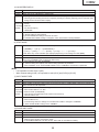
IMPORTANT SERVICE SAFETY PRECAUTION ........................................................................................ 2
SPECIFICATIONS ........................................................................................................................................ 5
OPERATION MANUAL ................................................................................................................................. 6
DIMENSIONS ............................................................................................................................................... 8
REMOVING OF MAJOR PARTS ..................................................................................................................9
ADJUSTING PROCEDURE OF EACH SECTION .....................................................................................13
PUBLIC MODE SETTING PROCEDURE ..................................................................................................32
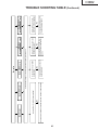
TROUBLE SHOOTING TABLE ..................................................................................................................38
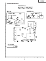
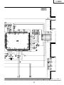
CHASSIS LAYOUT .....................................................................................................................................43
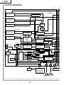
BLOCK DIAGRAM ......................................................................................................................................44
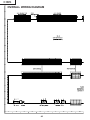
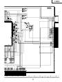
OVERALL WIRING DIAGRAM ...................................................................................................................46
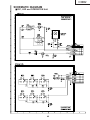
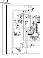
DESCRIPTION OF SCHEMATIC DIAGRAM ............................................................................................. 48
SCHEMATIC DIAGRAM ............................................................................................................................. 49
PRINTED WIRING BOARD ASSEMBLIES ................................................................................................71
REPLACEMENT PARTS LIST ....................................................................................................................81
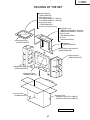
PACKING OF THE SET ..............................................................................................................................93
SHARP CORPORATION
This document has been published to be used for
after sales service only.
The contents are subject to change without notice.
LC-15B4U-S
LC-15B4U-B
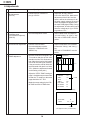
IMPORTANT SERVICE SAFETY PRECAUTION
Ë
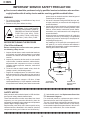
Service work should be performed only by qualified service technicians who are thoroughly familiar with all safety checks and the servicing guidelines which follow:
ground, such as electrical conduit or electrical ground
connected to an earth ground.
• Use an AC voltmeter having with 5000 ohm per volt,
or higher, sensitivity or measure the AC voltage drop
across the resistor.
• Connect the resistor connection to all exposed metal
parts having a return to the chassis (antenna, metal
cabinet, screw heads, knobs and control shafts,
escutcheon, etc.) and measure the AC voltage drop
across the resistor.
All checks must be repeated with the AC cord plug
connection reversed. (If necessary, a nonpolarized
adaptor plug must be used only for the purpose of
completing these checks.)
Any reading of 0.75V peak (this corresponds to 0.5
mA. peak AC.) or more is excessive and indicates a
potential shock hazard which must be corrected before
returning the monitor to the owner.
WARNING
1. For continued safety, no modification of any circuit
should be attempted.
2. Disconnect AC power before servicing.
A
V
CAUTION: FOR CONTINUED
PROTECTION AGAINST A RISK OF
FIRE REPLACE ONLY WITH SAME
TYPE F3701 (2.0A, 250V), F3702
(1.25A, 250V), F6500 (1.25A, 250V)
AND F6501 (1.25A, 250V) FUSE.
BEFORE RETURNING THE RECEIVER
(Fire & Shock Hazard)
Before returning the receiver to the user, perform
the following safety checks:
1. Inspect all lead dress to make certain that leads are
not pinched, and check that hardware is not lodged
between the chassis and other metal parts in the
receiver.
2. Inspect all protective devices such as non-metallic
control knobs, insulation materials, cabinet backs,
adjustment and compartment covers or shields,
isolation resistor-capacitor networks, mechanical
insulators, etc.
3. To be sure that no shock hazard exists, check for
leakage current in the following manner.
• Plug the AC cord directly into a 110~240 volt AC outlet,
and connect the DC power cable into the receiver's
DC jack. (Do not use an isolation transformer for this
test).
• Using two clip leads, connect a 1.5k ohm, 10 watt
resistor paralleled by a 0.15µF capacitor in series with
all exposed metal cabinet parts and a known earth
DVM
AC SCALE
1.5k ohm
10W
0.15 µF
TEST PROBE
TO EXPOSED
METAL PARTS
CONNECT TO
KNOWN EARTH
GROUND
12345678901234567890123456789012123456789012345678901234567890121234567890123456789012345678901212
12345678901234567890123456789012123456789012345678901234567890121234567890123456789012345678901212
12345678901234567890123456789012123456789012345678901234567890121234567890123456789012345678901212
SAFETY NOTICE
å" and shaded areas in the Replacement Parts Lists
and Schematic Diagrams.
For continued protection, replacement parts must be
identical to those used in the original circuit.
The use of a substitute replacement parts which do not
have the same safety characteristics as the factory
recommended replacement parts shown in this service
manual, may create shock, fire or other hazards.
Many electrical and mechanical parts in LCD television
have special safety-related characteristics.
These characteristics are often not evident from visual
inspection, nor can protection afforded by them be
necessarily increased by using replacement components
rated for higher voltage, wattage, etc.
Replacement parts which have these special safety
characteristics are identified in this manual; electrical
components having such features are identified by "
12345678901234567890123456789012123456789012345678901234567890121234567890123456789012345678901212
12345678901234567890123456789012123456789012345678901234567890121234567890123456789012345678901212
12345678901234567890123456789012123456789012345678901234567890121234567890123456789012345678901212
2
LC-15B4U-S
LC-15B4U-B
PRECAUTIONS A PRENDRE LORS DE LA REPARATION
Ë
Ne peut effectuer la réparation qu' un technicien spécialisé qui s'est parfaitement
accoutumé à toute vérification de sécurité et aux conseils suivants.
conduite électrique ou une prise de terre branchée à
la terre.
• Utiliser un voltmètre CA d'une sensibilité d'au moins
5000Ω/V pour mesurer la chute de tension en travers
de la résistance.
• Toucher avec la sonde d'essai les pièces métalliques
exposées qui présentent une voie de retour au châssis
(antenne, coffret métallique, tête des vis, arbres de
commande et des boutons, écusson, etc.) et mesurer
la chute de tension CA en-travers de la résistance.
Toutes les vérifications doivent être refaites après avoir
inversé la fiche du cordon d'alimentation. (Si
nécessaire, une prise d'adpatation non polarisée peut
être utilisée dans le but de terminer ces vérifications.)
Tous les courants mesurés ne doivent pas dépasser
0,5 mA.
Dans le cas contraire, il y a une possibilité de choc
électrique qui doit être supprimée avant de rendre le
récepteur au client.
AVERTISSEMENT
1. N'entreprendre aucune modification de tout circuit.
C'est dangereux.
2. Débrancher le récepteur avant toute réparation.
A
V
PRECAUTION: POUR LA
PROTECTION CONTINUE CONTRE
LES RISQUES D'INCENDIE,
REMPLACER LE FUSIBLE PAR UN
FUSIBLE DE MEME TYPE F3701
(2.0A, 250V), F3702 (1.25A, 250V),
F6500(1.25A, 250V), F6501(1.25A,
250V).
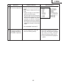
VERIFICATIONS CONTRE L'INCEN-DIE ET
LE CHOC ELECTRIQUE
Avant de rendre le récepteur à l'utilisateur, effectuer
les vérifications suivantes.
1. Inspecter tous les faisceaux de câbles pour s'assurer
que les fils ne soient pas pincés ou qu'un outil ne soit
pas placé entre le châssis et les autres pièces
métalliques du récepteur.
2. Inspecter tous les dispositifs de protection comme les
boutons de commande non-métalliques, les isolants,
le dos du coffret, les couvercles ou blindages de réglage
et de compartiment, les réseaux de résistancecapacité, les isolateurs mécaniques, etc.
3. S'assurer qu'il n'y ait pas de danger d'électrocution en
vérifiant la fuite de courant, de la facon suivante:
• Brancher le cordon d'alimentation directem-ent à une
prise de courant de 110-240V. (Ne pas utiliser de
transformateur d'isolation pour cet essai).
• A l'aide de deux fils à pinces, brancher une résistance
de 1.5kΩ 10 watts en parallèle avec un condensateur
de 0,15µF en série avec toutes les pièces métalliques
exposées du coffret et une terre connue comme une
VTVM
ECHELLE CA
1.5k ohm
10W
0.15 µF
SONDE D'ESSAI
AUX PIECES
BRANCHER A UNE
METALLIQUES
TERRE CONNUE
EXPOSEES
12345678901234567890123456789012123456789012345678901234567890121234567890123456789012345678901212
12345678901234567890123456789012123456789012345678901234567890121234567890123456789012345678901212
12345678901234567890123456789012123456789012345678901234567890121234567890123456789012345678901212
12345678901234567890123456789012123456789012345678901234567890121234567890123456789012345678901212
AVIS POUR LA SECURITE
identifiées par la marque " å " et hachurées dans la
liste des pièces de remplacement et les diagrammes
schématiques.
Pour assurer la protection, ces pièces doivent être
identiques à celles utilisées dans le circuit d'origine.
L'utilisation de pièces qui n'ont pas les mêmes
caractéristiques que les pièces recommandées par
l'usine, indiquées dans ce manuel, peut provoquer des
électrocutions, incendies, radiations X ou autres
accidents.
De nombreuses pièces, électriques et mécaniques,
dans les téléviseurs présentent des caractéristiques
spéciales relatives à la sécurité, qui ne sont souvent
pas évidentes à vue. Le degré de protection ne peut
pas être nécessairement augmentée en utilisant des
pièces de remplacement étalonnées pour haute tension,
puissance, etc.
Les pièces de remplacement qui présentent ces
caractéristiques sont identifiées dans ce manuel; les
pièces électriques qui présentent ces particularités sont
12345678901234567890123456789012123456789012345678901234567890121234567890123456789012345678901212
12345678901234567890123456789012123456789012345678901234567890121234567890123456789012345678901212
12345678901234567890123456789012123456789012345678901234567890121234567890123456789012345678901212
3
LC-15B4U-S
LC-15B4U-B
Precautions for using lead-free solder
1 Employing lead-free solder
"All PWBs" of this model employs lead-free solder. The LF symbol indicates lead-free solder, and is attached on
the PWBs and service manuals. The alphabetical character following LF shows the type of lead-free solder.
Example:
LFa
Indicates lead-free solder of tin, silver and copper.
2 Using lead-free wire solder
When fixing the PWB soldered with the lead-free solder, apply lead-free wire solder. Repairing with conventional
lead wire solder may cause damage or accident due to cracks.
As the melting point of lead-free solder (Sn-Ag-Cu) is higher than the lead wire solder by 40°C, we recommend
you to use a dedicated soldering bit, if you are not familiar with how to obtain lead-free wire solder or soldering bit,
contact our service station or service branch in your area.
3 Soldering
As the melting point of lead-free solder (Sn-Ag-Cu) is about 220°C which is higher than the conventional lead
solder by 40°C, and as it has poor solder wettability, you may be apt to keep the soldering bit in contact with the
PWB for extended period of time. However, Since the land may be peeled off or the maximum heat-resistance
temperature of parts may be exceeded, remove the bit from the PWB as soon as you confirm the steady soldering
condition.
Lead-free solder contains more tin, and the end of the soldering bit may be easily corroded. Make sure to turn on
and off the power of the bit as required.
If a different type of solder stays on the tip of the soldering bit, it is alloyed with lead-free solder. Clean the bit after
every use of it.
When the tip of the soldering bit is blackened during use, file it with steel wool or fine sandpaper.
Be careful when replacing parts with polarity indication on the PWB silk.
Lead-free wire solder for servicing
Part No,
★
Description
ZHNDAi123250E
J
φ0.3mm 250g(1roll)
ZHNDAi126500E
J
φ0.6mm 500g(1roll)
ZHNDAi12801KE
J
φ1.0mm
1kg(1roll)
4
Code
BL
BK
BM
LC-15B4U-S
LC-15B4U-B
SPECIFICATIONS
Items
Model
LCD panel
Number of dots
Video color systems
Destination
TV Standard (CCIR)
TV function
TV Tuning System
STEREO
CATV
Y/C FILTER
Brightness
Lamp life (Fluorescent lamp)
Viewing angles
Audio amplifier
Speakers
AV-IN1
AV-IN2
Terminals
COMPONENT
Antenna
Headphone
OSD language
Power supply
Weight
Accessories
LC-15B4U
15” Advanced Super View & BLACK TFT LCD
921,600 dots VGA
N358, N443, PAL, PAL-M, PAL-N, SECAM, PAL-60
USA/Latin America/Taiwan
NTSC/PAL-M/PAL-N
PLL 181 ch.
MTS+SAP
125 ch.
4-LINE COMB FILTER
430 cd/m2
60,000 hours
H: 170° V: 170°
2.1 W × 2
137/64 ×2 3/4 in. (4 × 7 cm), 2 pcs.
AV-IN1, S-VIDEO-IN
AV-IN2/AV-OUT
COMPONENT-IN, AUDIO-IN
F-Type
Mini-jack for stereo (ø3.5 mm)
English/French/Spanish
DC 12V, AC 110-240V, 50/60Hz
11.5 lbs. (5.2 kg), w/o accessories
Remote control, Battery (×2), Antenna cable, AC adapter,
AC cord, Cable clamp (×2), Operation manual
As a part of policy of continuous improvement, SHARP reserves the right to make design and specification changes for
product improvement without prior notice. The performance specification figures indicated are nominal values of
production units. There may be some deviations from these values in individual units.
5
6
CH
Remote control sensor
Speaker (Left)
VOL
Upper control panel
MAIN POWER
Note:
• TV/VIDEO, CH ( )/( ), VOL (+)/(–), and MENU on the main unit have the same functions as the same buttons
onthe remote control. Basically, this operation manual provides a description based on operation with the remote
control.
The SLEEP indicator lights up red when the
SLEEP TIMER is set.
SLEEP indicator
To change the vertical
angle of the LCD TV set,
tilt the screen up to 5
degrees forward or 10
degrees backward. The
TV set can also be
rotated 25 degrees to
right and left. Adjust the
angle so that the TV set
can be watched most
comfortably.
VOL (–)/(+)
CH ( )/( )
MENU
TV/VIDEO
MAIN POWER
Speaker (Right)
MENU TV/VIDEO
A green indicator lights when the power is
on and a red indicator lights when in the
standby mode (the indicator will not light
when the main power is off).
POWER indicator
Controls
AUDIO
R
L
PR
PB
ONENT
COMP
Y
AUDIO
R
VIDEO
UT
AV-IN2/O
L
Terminals
VIDEO
AUDIO
AUDIO
Y
PB
PR
AUDIO
AUDIO
(L)
(R)
(L)
(R)
S-VIDEO
AUDIO (R)
AUDIO (L)
VIDEO
POWER INPUT
(DC12V)
ANT. (Antenna terminal)
AV-IN
1
POWE
INPUTR
DC12V
USE TH
AC AD E SUPP
(PART APTER. LIED
NO. LOC
THE MO
ATED ON
DEL LAB
EL.)
ANT.
HEAD
PHON
E
S-VIDE
O
R
AUDIO
L
VIDEO
Carrying handle
Hold the carrying handle and tilt the
screen while steadying the stand with
your other hand.
HEADPHONE
AV-IN1
COMPONENT
AV-IN2/OUT
Adjusting the screen view angle
LC-15B4U-S
LC-15B4U-B
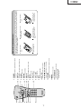
OPERATION MANUAL
9
8
6
7
5
2
3
4
1
SLEEP
POWER
VOL
MUTE
PIC. FLIP
CH
FLASHBACK
BRIGHT TV/VIDEO MENU
ENTER
DISPLAY
15
13
14
12
11
10
7
Set the channel.
15 Channel Select
Return to the previous channel.
14 FLASHBACK
Display the menu screen.
13 MENU
Select a Liquid Crystal Television input
source.
12 TV/VIDEO
Select a desired item on the screen.
11 '/"/\/| (Cursor control)
Set the orientation of the picture.
10 PIC. FLIP
Select audio settings.
9 MTS
Select channel.
8 CH ( )/( )
Set the volume.
7 VOL (+)/(–)
Mute the sound.
6 MUTE
Adjust the brightness of the screen.
5 BRIGHT
Execute a command.
4 ENTER
Set the sleep timer.
3 SLEEP
Display the channel and time information.
2 DISPLAY
Switch the Liquid Crystal Television power
on or off.
1 POWER
1
Slide the cover while
pressing the (") part.
Open the battery
cover.
2
–
+
Position the positive and
negative ends of the batteries
as indicated in the compartment.
+
–
Insert two (“AAA” size, UM/
SUM-4) batteries.
3
Engage the claw on the
cover into the battery
housing and slide shut.
Close the battery
cover.
Before using the LCD TV set for the first time, install two (“AAA” size, UM/SUM-4) batteries (supplied).
When the batteries become depleted and the remote control fails to operate, replace the batteries with
new (“AAA” size, UM/SUM-4) batteries.
Batteries for the Remote Control
LC-15B4U-S
LC-15B4U-B
LC-15B4U-S
LC-15B4U-B
DIMENSIONS
2 9/32 (58)
CH
MENU TV/VIDEO MAIN POWER
1211/16 (322.2)
1159/64 (303)
93/32 (231)
6 3/64 (153.5)
125/64 (307)
1/32 (1)
33/32 (78.7)
151/64 (381.7)
57/8 (149.5)
193/64 (484)
231/64 (63.2)
VIDEO
AV-IN 2/OUT
L
AUDIO
R
COMPONENT
Y
VIDEO
AV-IN1
L
AUDIO
R
S-VIDEO
HEAD
PHONE
PB
ANT.
PR
USE THE SUPPLIED
AC ADAPTER.
(PART NO. LOCATED ON
THE MODEL LABEL.)
L
POWER
INPUT
DC12V
AUDIO
1
/32 (1)
R
751/64 (198)
11/2 (38.2)
315/16 (100)
1413/32 (366.2)
315/16 (100)
8
2 31/64 (63.2)
Unit: inch (mm)
LC-15B4U-S
LC-15B4U-B
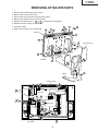
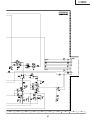
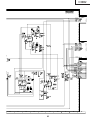
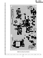
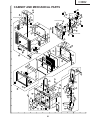
REMOVING OF MAJOR PARTS
1. Remove the stand fixing screws (4 pcs.).
2. Remove the two terminal covers.
3. Remove the terminal section fixing screws (2 pcs.).
4. Remove the cabinet B fixing screws (8 pcs.).
5. Cabinet A is opend order of 5-1 to 5-8 , and detach the Cabinet B.
6. Release the wire holders at 2 locations.
7. Peel off the tape.
4
8. Detach the connector from each PWB.
4
5-4
5-6
5-5
4
5-3
Cabinet A
5-2
5-7
2
Terminal cover (L)
4
2
5-1
5-8
Terminal
cover (S)
Cabinet B
3
Stand
OPERATION PWB
8
8
8
8
8
P4001
SC1203
7
Tape
SC2001
SC1202
P6500
MAIN PWB
8
8
SC1204
8
8
P1201
P701
P6502
8
SC2002
SC3403
6
Wire holder
TUNER PWB
8
8
P8401
P3701
8
P3601
P3302
P3301
8
8
P3502
8
P3603
P4004
8
7
RC/LED PWB
Tape
9
P6501
INVERTER PWB
1
LC-15B4U-S
LC-15B4U-B
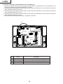
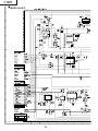
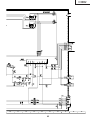
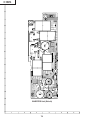
9. Remove the inverter PWB fixing screws (2 pcs.).
10. Remove the main PWB fixing screws (3 pcs.).
11. Detach the chassis frame cover.
12. Remove the tuner PWB fixing screws (3 pcs.) .
13. Remove the R/C, LED PWB fixing screws (2 pcs.).
14. Remove the operation PWB fixing screws (2 pcs.).
15. Remove the chassis frame fixing screws (2 pcs.).
16. Remove the LCD panel unit fixing screws (2 pcs.).
9
10
INVERTER PWB
MAIN PWB
12
TUNER PWB
15
15
11
Chassis Frame
Chassis Frame Cover
OPERATION PWB
14
LCD Panel unit
16
R/C, LED PWB
13
10
LC-15B4U-S
LC-15B4U-B
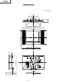
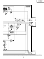
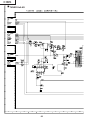
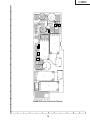
» Precautions in handling the LCD panels
1. Work in a clean room (with humidities below 50%).
2. Be sure to wear an anti-static armband.
3. Handle the panels on an electroconductive mat.
4. Be careful not to fall, shake and shock the panels.
17. Remove the LCD panel unit fixing screws (4 pcs.).
18. Detach the prism sheet, diffusion sheet and reflection/deflection sheet.
19. Detach the four reflection mirrors.
20. Remove the lamp unit.
21. Detach the lamp guide plate.
22. Detach the two lamp reflection sheets.
19 Reflection Mirror
Back Shield
(PSLDM4689CEFW)
Light Guide Plate
(PGiDM0070CEZZ)
Lamp Unit
(KLMP-0122CEZZ)
21
20
Reflection Sheet (Cover)
(PSHEP0307CEZZ)
Prism Sheet
(PSHEP0282CEZZ)
19 Reflection Mirror
17
22
Reflection Sheet-2
(PSHEP0285CEZZ)
17
17
18
LCD Panel Unit
Reflection Sheet-1
(PSHEP0284CEZZ)
17
Diffusion Sheet
(PSHEP0283CEZZ)
Reflection/deflection Sheet
(PSHEP0281CEZZ)
11
LC-15B4U-S
LC-15B4U-B
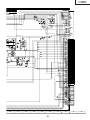
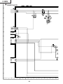
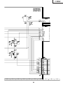
Precautions at the time of the side B(back) service of digital unit.
1. Remove only SC2002 of the FFC for connection between Main unit (SC2002) and Tuner unit(SC3403), and
connect the extended cable (QCNW-A556WJZZ) for service.
2. Remove the FFC for connection between Main unit (SC1204) and LCD panel unit, and connect the extended
cable (QCNW-A553WJZZ) for service.
3. Remove the FFC for connection between Main unit (SC1203) and LCD panel unit, and connect the extended
cable (QCNW-A556WJZZ) for service.
4. Remove the FFC for connection between Main unit (SC1202) and LCD panel unit, and connect the extended
cable (QCNW-A555WJZZ) for service.
5. Remove the main unit fixing screws (3 pcs.), a substrate is reversed.
5
P4001
SC1203
SC2001
SC1202
3
4
MAIN PWB
SC1204
2
P1201
P701
INVERTER PWB
1
SC2002
SC3403
TUNER PWB
P8401
P3701
Step
1
2
3
4
Part No.
QCNW-A556WJZZ
QCNW-A553WJZZ
QCNW-A556WJZZ
QCNW-A555WJZZ
Description
Extension Cable 50-pin Main (SC2002)-Tuner (SC3403)
Extension Cable 30-pin Main (SC1204)-LCD Panel
Extension Cable 50-pin Main (SC1203)-LCD Panel
Extension Cable 20-pin Main (SC1202)-LCD Panel
12
LC-15B4U-S
LC-15B4U-B
ADJUSTING PROCEDURE OF EACH SECTION
The best adjustment is made before shipping. If any position deviation is found or after part replace is performed, adjust
as follows.
1. Preparation for Adjustments
Use the exclusive-use AC adapter or stable DC power supply.
AC adapter: UADP-A009WJPZ
DC power supply: 12 ± 0.5V
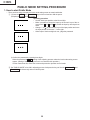
2. Special mode setting procedure
(1)After initialization of E2PROM the mode is changed to the adjustment mode.
[Procedure]
Connect TP2001 and TP2002 to GND, and turn on the power.
[Description]
» The initialization of microprocessor is as follows.
» AV position, DAC data, G/A data, sound processor data, and video chroma data adjustment values are taken
as defaults.
(2)Adjustment mode
[Procedure]
Short-circuit TP2001 to GND, and turn on the power.
Or short-circuit TP2002 to GND, and turn on the power.
Or holding down the "TV/VIDEO" key and "MENU" key, turn on the main power, and simultaneously press the
(inspection process) "CH (Ù)" key and "VOL(–) " key to change the mode to the adjustment mode.
[Description]
The manual adjustment or adjustment through communication with the automatic machine is performed.
(3)Shipping setting mode
[Procedure]
Holding down the "TV/VIDEO" key and "MENU" key, turn on the main power, and simultaneously press the
(inspection process) "CH (ù)" key and "VOL(+)" key to change the mode to the shipping setting mode.
Note: Keep it in mind to turn off the power immediately. If any key-in is accidentally made, the setting will be
canceled.
[Description]
User adjustment and other values are taken as defaults.
If TV is indicated as SETTING COMPLETE, setting has been completed.
3. Cancel of special mode
Turn off the main unit power.
13
LC-15B4U-S
LC-15B4U-B
4. Adjustments
Adjustment
Adjusting conditions
Adjusting method
1
B+ Adjustment
(R3714)
1. Connect the DC voltmeter to
pin (4) of P3701.
1. Adjust the "B+ Adj" value to
5.0±0.02V with R3714. Make exact
adjustment of the 5.00V level because it will be the reference for all
the other supply voltages. Be sure to
make this adjustment together with
the main PWB (digital PWB). During
the adjustment, be also careful not to
allow the voltage at pin (2) of P3701
to go above 5.3 V.
2
Inch Size setup
(If E2PROM is replaced)
(IC2010)
1. Go to the adjustment mode.
1. Select "INCH SIZE" and adjust to
"15" with "VOL(+)" or "VOL(–)" key.
* The color of "INCH SIZE" must be
yellow.
3
Common-bias adjustment 1. Receive a B/W channel.
2. Go to the adjustment mode.
3. Select the "COM BIAS" with
"MENU" key.
1. Adjust "COM BIAS" to the darkest
screen with "VOL(+)" and "VOL(–)"
key.
* The color of "COM BIAS" must be
yellow.
4
TAMP adjustment
1. Receive a half color bar signal in the
TV mode so that the top left zone
should turn white 75% as shown below. Other signal can be fed instead
of the half color bar signal, however,
if the point at the vertical 180th line
and horizontal 46th pixel is of white
75%. (Make the adjustment based
on the setting of this point.)
2. Adjust the "NTSC TAMP" setting on
page 2 of adjustment process mode
so that the "Y" reading on the same
page should be 187 - 202.
White 75% at
top left zone
Vertical 180th line and
horizontal 46th pixel
480 lines
640 pixels
2
3. Make the same setting for the PALM TAMP and PAL-N TAMP data.
COM BIAS
118
TAMP L
187
TDATA
–
TAMP H
202
NTSC TAMP
20
PAL-M TAMP
20
PAL-N TAMP
20
"Y" data
↑ On usual screen ("Y" data is not exact.)
2
NTSC TAMP
YDATA
20
187 *** 202
"Y" data
↑ On single-item screen ("Y" data is exact.)
14
LC-15B4U-S
LC-15B4U-B
Adjustment
5
Adjusting conditions
White balance adjustment 1. Receive the monoscope pattern
signal.
2. Select Page 3 of Adjustment Process
mode.
3. * Adjust the upper six items before
going to the six D2 items.
* Once the upper six items have been
adjusted, their respective D2 items
are now self-adjusted to the same
settings or add-on settings.
Readjust the D2 items as required.
* Even when the D2 items have been
readjusted, the upper six items stay
intact.
Adjusting method
3
RCUTOFF
GCUTOFF
BCUTOFF
R-GAIN
G-GAIN
B-GAIN
D2 RCUTOFF
D2 GCUTOFF
D2 BCUTOFF
D2 R-GAIN
D2 G-GAIN
D2 B-GAIN
0
0
0
0
0
0
0
0
0
0
0
0
Red cut-off adjustment
Green cut-off adjustment
Blue cut-off adjustment
White balance
White balance
White balance
Red cut-off adjustment (D2)
Green cut-off adjustment (D2)
Blue cut-off adjustment (D2)
White balance (D2)
White balance (D2)
White balance (D2)
D2:COMPONENT 480P INPUT
6
Checking and modifying
the settings adjustment
(If E2PROM is replaced)
Go to the adjustment mode and
check the following settings.
15
See if all the settings are as specified. If not, select an item in question
with "VOL(+)" or "VOL(–)" key and
adjust the setting as shown at left.
* An item selected will be highlighted
in yellow.
LC-15B4U-S
LC-15B4U-B
Adjustment
7
E2PROM data write
Adjusting conditions
Adjusting method
1. Call up the adjustment process menu If the wrong data has been sent:
and get Page 6 displayed on-screen. 1. Initialize the E 2 PROM. (Take the
special mode setting procedure (1).)
2. Enter "A40000002681" for the "I2C
DATA" item in Line 1.
2. Take the adjustment steps 2 thru 7.
3. Move the cursor to the "I 2C DATA"
item in Line 2 and carry out "SEND"
with the right cursor key.
5. Shipping setting list
EZ SETUP AUTO START .............................................................................................. ON
LANGUAGE .................................................................................................................... ENGLISH
LAST CHANNEL ............................................................................................................. 2ch
LAST TV/INPUT ............................................................................................................. TV
LAST AIR/CATV ............................................................................................................. AIR
SKIP DATA_CATV ......................................................................................................... ALL SKIP
SKIP DATA_AIR ............................................................................................................. ALL SKIP
VOLUME ......................................................................................................................... 20
SLEEP TIMER
SLEEP TIMER ........................................................................................................... CLEAR
VIDEO ADJUST
PICTURE ................................................................................................................... 50
TINT ........................................................................................................................... 0
COLOR ...................................................................................................................... 0
BLACK LEVEL ........................................................................................................... 0
SHARPNESS ............................................................................................................. 0
RED-BLUE ................................................................................................................. 0
GREEN ...................................................................................................................... 0
COLOR SYSTEM ...................................................................................................... N358
PRESET
BRIGHTNESS ........................................................................................................... BRIGHT
MTS ........................................................................................................................... STEREO
AUTO POWER OFF .................................................................................................. OFF
PICTURE FLIP .......................................................................................................... NORMAL
AV21N/OUT ............................................................................................................... IN
CLOSED CAPTION
CC/TEXT ................................................................................................................... OFF
V-CHIP BLOCK
SECRET No. (V-CHIP) .............................................................................................. CLEAR
MPAA RATING .......................................................................................................... NONE(ALL ---)
GUIDELINE RATING ................................................................................................. NONE(ALL ---)
GUIDELINE CONTENTS .......................................................................................... ALL UNBLOCK(BLANK)
CDN.ENGLISH RATING ........................................................................................... NONE(ALL ---)
CDN.FRENCH RATING ............................................................................................ NONE(ALL ---)
V-CHIP STATUS ....................................................................................................... OFF
SET UP
BLUE SCREEN ......................................................................................................... OFF
CLOCK
CLOCK ...................................................................................................................... AUTO CLOCK
EDS CH SET ............................................................................................................. AUTO
EDS CH(AUTO) ......................................................................................................... (NOT DETERMINED)
EDS CH(MANUAL) .................................................................................................... 2
TIME .......................................................................................................................... 12:00AM
DST ............................................................................................................................ OFF
16
LC-15B4U-S
LC-15B4U-B
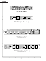
Test patterns in adjustment process mode
[1] IC801 (Video decoder) test patterns
1-1. Getting the test patterns displayed
Put the screen in AV1, AV2 or COMPONENT but keep out any signal. Call the adjustment process mode,
select "TEST PATTERN" in the 3rd line of VPC 1, make the settings 1 thru 6, and the following test patterns
show up.
1-2. Test patterns
» Setting 1
Cyan
Magenta
Yellow
green
Blue
Red
Green
Magenta
Cyan
Green
Yellow
The color bars are displayed as shown at left.
» Setting 2
Finer vertical stripes than Setting 1 are displayed.
» Setting 3
The green pattern is displayed as shown at left.
Green
Bright
Dark
Bright
» Setting 4
A rather dark green-only pattern is displayed.
» Setting 5
A half-tone green-only pattern is displayed.
» Setting 6
A rather bright green-only pattern is displayed.
[2] IC1201 (LCD controller) test pattern
2-1. Getting the test pattern displayed
Put the screen in AV1, AV2 or COMPONENT but keep out any signal. Call the adjustment process mode,
select "TEST PATTERN" in the 3rd line of DPS 1, turn on the setting, and the following test pattern shows up.
2-2. Test pattern
The following test pattern appears.
Dark
Gray scale
Bright
Dark
Dark
Dark
Dark
Red
Green
Blue
Bright
Bright
Bright
Dark
Dark
Dark
Black
Gray
Gradation
White
Note: When the IC801 and IC1201 test pattern display commands are both turned on at the same time, the IC1201
test pattern is given priority.
17
LC-15B4U-S
LC-15B4U-B
Pin functions of microprocessor IC (IC2001) RH-iXA620WJZZQ
In Power Saving*
Pin No.
Name of Terminal
I/O
Within 1 min. after
Name of Function
Function in Normal Times
Power-OFF by R/C Unit
1
2
3
4
5
6
7
8
9
10
11
12
13
14
15
16
17
18
19
20
21
22
23
24
25
26
27
28
29
30
31
32
33
34
35
36
37
38
39
40
41
42
43
44
45
46
47
48
49
50
VHOLD1
HLF1
P94/DA1/SCL3/RXD2
P93/DA0/SDA3/TXD2
P92/TB2IN/DIGR0
P91/TB1IN
P90/TB0IN
BYTE
CNVSS
P87/XCIN/DIGG0
P86/XCOUTDIGB0
RESET
XOUT
VSS
XIN
VCCI
OSC1/OSCHLF
OSC2
P83/INT1
P82/INT0
OUT1
OUT2
P77/HC1
P76/TA3OUT
P75/HC0
P74/TA2OUT
P73/CTS2, RTS2
P72/SCL2/CLK2
P71/SCL1/RXD2
P70/SDA1/TXD2
P67/SDA2
R/DIGR1
G/DIGG1
B/DIGB1
P63/TXD0
P62/RXD0
P61/CLK0
P60/CTS0/RTS0
P57/RDY/CLKOUT
P56/ALE
P55/HOLD
P54/HLDA
P53/BCLK
P52/RD
P51/WRH/BHE
P50/WRL/WR
P47/CS3
P46/CS2
P45/CS1
P44/CS0
I
I/O
O
O
O
I
I
O
O
I
O
I
O
I
I
I
I
O
I
O
O
O
O
O
O
O
I
I/O
I/O
I/O
I/O
O
O
O
O
I
I
O
O
O
I
I
O
O
O
I
O
O
O
O
Vhold
HLF
L
L
L
Hi-Z
Hi-Z
Hi-Z
L
L
L
L
L
L
L
Hi-Z
Hi-Z
Hi-Z
Hi-Z
Hi-Z
L
L
L
TIMELED
CSYNC
IREM1
BYTE
CNVss
Xcin
Xout
RESET
Xout
Vss
Xin
Vccl
OSCin
PSWin
BLK
DAC1CS
MRDY
SCL2
SCL1
SDA1
SDA2
OSD_R
OSD_G
OSD_B
SUBDout
SUBDin
SCLK
BUSY
MAIN SW
L
Hi-Z
L
L
L
L
L
L
L
EPM
L_ERR
S IN/OUT
PC/VD
CE
AV1/AV2
TV/AV
VSHOUT
* Except for AUTO CLOCK being in operation when the power is OFF
18
For CLOSED CAPTION
For CLOSED CAPTION
N.C.
For LED lighting in timer operation
N.C.
Composite sync signal
Remote control
GND
GND (“H” at the time of flash writing)
32 kHz oscillation input
32 kHz oscillation output
Reset state at “L”
Microprocessor oscillator connection
GND
Microcomputer oscillator connection
Power supply (3.3 V)
Clock input for OSD
N.C.
Power supply monitor (“L” at the time of power-ON)
N.C.
OSD blanking output
Not Used
Gray scale control IC chip selection
N.C.
N.C.
N.C.
I2C bus open connection selection input
I2C bus serial clock line 2 (EEPROM)
I2C bus serial clock line 1 (UV TUNER, VPC, MSP, 3D YC, DPS)
I2C bus serial data line 1
I2C bus serial data line 2
R signal output of OSD
G signal output of OSD
B signal output of OSD
(T x D at flash WRITE)
(R x D at flash WRITE)
Clock input at flash WRITE
Busy output at flash WRITE
Main SW ON “H”/OFF “L” (LED power supply control)
N.C.
“L” at flash WRITE
Fluorescent lamp error detection processing (Error at “H”)
Audio input/output selection (Audio output at “L”)
D2 (& PC) mode selection (D2 or PC mode at “L”)
N.C.
“H” at flash WRITE
AV selector SW
AV selector SW
N.C.
Panel gate driver voltage control
LC-15B4U-S
LC-15B4U-B
In Power Saving*
Pin No.
Name of Terminal
I/O
Within 1 min. after
Name of Function
Function in Normal Times
Power-OFF by R/C Unit
51
52
53
54
55
56
57
58
59
60
61
62
63
64
65
66
67
68
69
70
71
72
73
74
75
76
77
78
79
80
81
82
83
84
85
86
87
88
89
90
91
92
93
94
95
96
97
98
99
100
P43/A19
P42/A18
P41/A17
P40/A16
P37/A15
P36/A14
P35/A13
P34/A12
P33/A11
P32/A10
P31/A9
HSYNC
P30/A8
VSYNC
P27/A7
P26/A6
P25/A5
P24/A4
P23/A3
P22/A2
P21/A1
P20/A0
P17/D15
P01/D1
P15/D13
P14/D12
P13/D11
P12/D10
P11/D9
P10/D8
P07/D7
P06/D6
P05/D5
P04/D4
P03/D3
P02/D2
P01/D1
P00/D0
P107/AN5/DIGR2
P106/AN4/DIGG2
P105/AN3/DIGB2
P104/AN2
P103/AN1
P102/AN0
VHOLD2
HLF2
CVIN2
TVSETB
VCCE
CVIN1
O
O
O
O
I
O
I
O
O
O
O
I
O
I
O
O
O
O
O
O
O
O
I
O
O
O
O
O
O
O
I
I
O
O
O
O
I
I
I
I
I
I
I
O
I
I/O
I
I
I
I
L
L
L
L
Hi-Z
L
Hi-Z
L
L
L
L
REQ
LED_POW
SP MUTE 1
CVBS/Y
HP DET
SSTBY
VSH IN
LMUTE
V IN/OUT
SRESET
HSYNC
L
VSYNC
L
L
L
L
L
L
L
L
Hi-Z
L
L
L
L
L
L
L
Hi-Z
Hi-Z
L
L
L
L
Hi-Z
Hi-Z
Hi-Z
Hi-Z
Hi-Z
Hi-Z
Hi-Z
L
POWout
ADPPOW
DACOUTCON
MP_DA
MP_CLK
DDC_RESET
KEY4
KEY5
POWin
SSW
AFT
AGC
KEY1
KEY2
V HOLD2
HLF2
CVin2
TVSETB
VccE
CVin1
* Except for AUTO CLOCK being in operation when the power is OFF
19
Adjusting process
Green by TV power supply LED control at “H”, and red at “L”
Main speaker MUTE
CVBS/Y selection (AV selector SW)
Headphone detection (Headphone at “L”)
Speaker standby (“L” at standby)
Panel gate driver voltage check (Standby maintained at “H”)
Line-out audio MUTE (Audio output MUTE at “H”)
Image input/output selection (Image output at “L”)
“L” output at multi-Sound IC (MSP) reset
N.C.
Horizontal sync signal for OSD
N.C.
Vertical sync signal for OSD
N.C.
N.C.
N.C.
N.C.
N.C.
N.C.
N.C.
DC/DC control output
Adaptor ON/OFF input
Gray scale control IC for output control (Output at “H”)
N.C.
N.C.
N.C.
Gray scale control IC for data output
Gray scale control IC for clock output
“L” output at VPC, G/A, 3DY/C, DPS reset
Key input 4
Key input 5
N.C.
N.C.
N.C.
N.C.
DC/DC start detection (Detection at “H”)
S terminal by S terminal connection at “L”
AFT voltage input
AGC input voltage
Key input 1
Key input 2
SLOW SW
N.C.
For CLOSED CAPTION
For CLOSED CAPTION
For CLOSED CAPTION
For CLOSED CAPTION (For test, L fixed)
Power supply (5V)
For CLOSED CAPTION
LC-15B4U-S
LC-15B4U-B
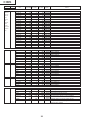
Table of Adjusting Process Defaults
1000 order
100 and 10 orders
Title No.
Page No.
0
1
Item
MODEL
INCH SIZE
ERROR NO RESET
PUBLIC MODE
V-CHIP
CANADIAN VCHIP
EXT CONTROL
VPC SHARPNESS
Initial Values Min. Value
Max. Value
Content
←
A620
15
0
OFF
1
OFF
OFF
ON
Display
0
→
5
→
→
→
→
→
13/15/20
Decimal
ON/OFF
1/2
ON/OFF
ON/OFF
ON/OFF
Selection of model name (For prevention of malfunction, it is
impossible to change it.)
Selection of screen size (inch)
Lamp error count and reset
Hotel mode setting
VCHIP line MUTE setting
Setting for responding to CANADIAN VCHIP
Bus, UART opening ON/OFF (OSD display is not changed.)
Adjustment or no adjustment of SHARPNESS by VPC (No effect by D2)
Opposed bias adjustment
Setting Y lower limit value in TAMP adjustment
Data READ value in TAMP adjustment
Setting Y upper limit value in TAMP adjustment
TAMP adjustment
TAMP adjustment
TAMP adjustment
EDS data captured is displayed at the top.
ROM and GAIBU version No. are displayed at the bottom.
0
2
COM BIAS
TAMP L
YDATA
TAMP H
NTSC TAMP
PAL-M TAMP
PAL-N TAMP
0
3
RCUTOFF
GCUTOFF
BCUTOFF
R-GAIN
G-GAIN
B-GAIN
D2 RCUTOFF
D2 GCUTOFF
D2 BCUTOFF
D2 R-GAIN
D2 G-GAIN
D2 B-GAIN
0
4
I2C DATA
I2C DATA
SOUND
VPC
DPS
DAC
TUNER
OTHERS
1
SOUND1 VOLUME
AVC
MSP DATA
MSP DATA
CARRIER MUTE
SP TEST
1
SOUND2 PRESCALE SCART
PRESCALE FM/AM-M
IGR THR
110
187
–
202
20
20
20
0
0
0
0
0
0
0
255
255
255
255
63
63
63
Decimal
Decimal
Decimal
Decimal
Decimal
Decimal
Decimal
0
0
0
0
0
0
0
0
0
0
0
0
-63
-63
-63
-63
-63
-63
-63
-63
-63
-63
-63
-63
63
63
63
63
63
63
63
63
63
63
63
63
+/- decimal
+/- decimal
+/- decimal
+/- decimal
+/- decimal
+/- decimal
+/- decimal
+/- decimal
+/- decimal
+/- decimal
+/- decimal
+/- decimal
Red cut-off adjustment
Green cut-off adjustment
Blue cut-off adjustment
White balance
White balance
White balance
Red cut-off adjustment (D2)
Green cut-off adjustment (D2)
Blue cut-off adjustment (D2)
White balance (D2)
White balance (D2)
White balance (D2)
I2C BUS control IC data WRITE and READ
Execution of WRITE and READ
Goes to SOUND adjustment page.
Goes to VPC adjustment page.
Goes to DPS adjustment page.
Goes to DAC adjustment page.
Goes to TUNER adjustment page.
Goes to other adjustment page.
20
OFF
0
60
→
0
WAIT
ON
OFF
–
–
–
–
→
→
27
33
12D
0
0
0A0
Decimal
OFF/8SEC
/4SEC
/2SEC/20MS
–
–
ON/OFF
OFF/LR
127
Decimal
127
Decimal
7F0 Hexadecimal
20
Volume
AVC setting
Sound IC MSP data WRITE and READ
Execution of WRITE and READ
Sound output setting without TV sync
For sound test
Pre-scale setting (External input)
Pre-scale setting (TV)
IGR Thresh level
LC-15B4U-S
LC-15B4U-B
1000 order
100 and 10 orders
Title No.
Page No.
1
SOUND3 EXT GEQ BAND1
EXT GEQ BAND2
EXT GEQ BAND3
EXT GEQ BAND4
EXT GEQ BAND5
TV GEQ BAND1
TV GEQ BAND2
TV GEQ BAND3
TV GEQ BAND4
TV GEQ BAND5
+1.0
+1.5
-1.5
-0.5
+0.5
+1.0
+1.5
-1.5
-0.5
+0.5
1
SOUND4 MDB
LVL
FRQ
STR
LMT
HMC
HPF
LPF
OFF
00
50
00
00
00h
20
50
2
VPC1
VPC DATA
VPC DATA
TEST PATTERN
AUTO LCK
NTSC AVO STOP
PAL AVO STOP
CBW N358
CBW OTHERS
AUTO LDLY
FP12TIM
0
WAIT
0
10
0
858
2
1
0
700
–
–
0
0
0
0
0
0
-7
0
–
–
–
–
6
Decimal
4094
Decimal
2047
Decimal
2047
Decimal
3
Decimal
3
Decimal
1 +/- decimal
1000 Unit 100/Decimal
Image IC VPC data WRITE and READ
Execution of WRITE and READ
VPC test pattern selection
Line lock mode selection
Horizontal position setting (at N358)
Horizontal position setting (at other than N358)
Chroma band pass setting (at N358)
Chroma band pass setting (at other than N358)
Y/C phase setting
Measures against up/down bound
2
VPC2
NOSEL
DDR
HDG
VDG
VPK
KILVL 08
KILHY 05
VSYNC DELAY
D2 VSYNC DELAY
DVCO
D2 DVCO
3
0
2
1
3
08
05
7
7
-720
1000
0
0
0
0
0
0
0
0
0
-2048
-2048
3
Decimal
3
Decimal
3
Decimal
3
Decimal
15
Decimal
FF Hexadecimal
FF Hexadecimal
255
Decimal
255
Decimal
2047 +/- decimal
2047 +/- decimal
COM filter setting
COM filter setting
COM filter setting
COM filter setting
COM filter setting
Color killer level setting
Color killer hysteresis setting
V sync phase setting (in normal times)
V sync phase setting (at 480P)
DVCO setting (in normal times)
DVCO setting (at 480P)
2
VPC3
N358 AVO START
N358 SFIF
N358 SCINC1
N358 AV LDLY
N358 TV LDLY
N358 PEAKING FILTER
N358 TV H-PEAKING
N358 AV H-PEAKING
N358 TV CORING
N358 AV CORING
139
0
1635
0
0
0
2
2
1
1
0
0
1024
-7
-7
0
0
0
0
0
1023
4095
4095
1
1
2
7
7
1
1
Decimal
Decimal
Decimal
+/- decimal
+/- decimal
Decimal
Decimal
Decimal
Decimal
Decimal
Horizontal position setting
Horizontal position setting
Circularity setting
Y/C phase setting (composite, S-image)
Y/C phase setting (TV)
Peaking filter setting (TV, composite, S-image)
Image sharpness setting (TV)
Image sharpness setting (composite, S-image)
Image sharpness setting 2 (TV)
Image sharpness setting 2 (composite, S-image)
2
VPC4
N358 TV CONTRAST
N358 AV CONTRAST
N358 TV COLOR
N358 AV COLOR
N358 TV TINT
N358 AV TINT
N358 BRIGHTNESS
48
48
2070
2070
-10
-10
16
0
0
0
0
-512
-512
-128
63
63
4094
4094
512
512
127
Decimal
Decimal
Decimal
Decimal
+/- decimal
+/- decimal
+/- decimal
Image setting (TV)
Image setting (composite, S-image)
Color depth setting (TV)
Color depth setting (composite, S-image)
Hue setting (TV)
Hue setting (composite, S-image)
Brightness setting (TV, composite, S-image)
Item
Initial Values Min. Value
-12.0
-12.0
-12.0
-12.0
-12.0
-12.0
-12.0
-12.0
-12.0
-12.0
Max. Value
+12.0
+12.0
+12.0
+12.0
+12.0
+12.0
+12.0
+12.0
+12.0
+12.0
Display
Unit 0.5
+/- decimal
ON/OFF
21
Content
Equalizer setting 1 (External input)
Equalizer setting 2 (External input)
Equalizer setting 3 (External input)
Equalizer setting 4 (External input)
Equalizer setting 5 (External input)
Equalizer setting 1 (TV)
Equalizer setting 2 (TV)
Equalizer setting 3 (TV)
Equalizer setting 4 (TV)
Equalizer setting 5 (TV)
MDB
LC-15B4U-S
LC-15B4U-B
1000 order
100 and 10 orders
Title No.
Page No.
2
VPC5
PAL-M AVO START
PAL-M SFIF
PAL-M SCINC1
PAL-M AV LDLY
PAL-M TV LDLY
PAL-M PEAKING FILTER
PAL-M TV H-PEAKING
PAL-M AV H-PEAKING
PAL-M TV CORIMGf
PAL-M AV CORING
139
0
1635
0
0
0
2
2
1
1
0
0
1024
-7
-7
0
0
0
0
0
1023
4095
4095
1
1
2
7
7
1
1
Decimal
Decimal
Decimal
+/- decimal
+/- decimal
Decimal
Decimal
Decimal
Decimal
Decimal
Horizontal position setting
Horizontal position setting
Circularity setting
Y/C phase setting (composite, S-image)
Y/C phase setting (TV)
Peaking filter setting (TV, composite, S-image)
Image sharpness setting (TV)
Image sharpness setting (composite, S-image)
Image sharpness setting 2 (TV)
Image sharpness setting 2 (composite, S-image)
2
VPC6
PAL-M TV CONTRAST
PAL-M AV CONTRAST
PAL-M TV COLOR
PAL-M AV COLOR
PAL-M TV TINT
PAL-M AV TINT
PAL-M BRIGHTNESS
48
48
2070
2070
0
0
16
0
0
0
0
-512
-512
-128
63
63
4094
4094
512
512
127
Decimal
Decimal
Decimal
Decimal
+/- decimal
+/- decimal
+/- decimal
Image setting (TV)
Image setting (composite, S-image)
Color depth setting (TV)
Color depth setting (composite, S-image)
Hue setting (TV)
Hue setting (composite, S-image)
Brightness setting (TV, composite, S-image)
2
VPC7
PAL-N AVO START
PAL-N SFIF
PAL-N SCINC1
PAL-N AV LDLY
PAL-N TV LDLY
PAL-N PEAKING FILTER
PAL-N TV H-PEAKING
PAL-N AV H-PEAKING
PAL-N TV CORING
PAL-N AV CORING
139
0
1635
0
0
0
2
2
1
1
0
0
1024
-7
-7
0
0
0
0
0
1023
4095
4095
1
1
2
7
7
1
1
Decimal
Decimal
Decimal
+/- decimal
+/- decimal
Decimal
Decimal
Decimal
Decimal
Decimal
Horizontal position setting
Horizontal position setting
Circularity setting
Y/C phase setting (composite, S-image)
Y/C phase setting (TV)
Peaking filter setting (TV, composite, S-image)
Image sharpness setting (TV)
Image sharpness setting (composite, S-image)
Image sharpness setting 2 (TV)
Image sharpness setting 2 (composite, S-image)
2
VPC8
PAL-N TV CONTRAST
PAL-N AV CONTRAST
PAL-N TV COLOR
PAL-N AV COLOR
PAL-N TV TINT
PAL-N AV TINT
PAL-N BRIGHTNESS
48
48
2070
2070
0
0
16
0
0
0
0
-512
-512
-128
63
63
4094
4094
512
512
127
Decimal
Decimal
Decimal
Decimal
+/- decimal
+/- decimal
+/- decimal
Image setting (TV)
Image setting (composite, S-image)
Color depth setting (TV)
Color depth setting (composite, S-image)
Hue setting (TV)
Hue setting (composite, S-image)
Brightness setting (TV, composite, S-image)
2
VPC9
PAL AVO START
PAL SFIF
PAL SCINC1
PAL AV LDLY
PAL PEAKING FILTER
PAL AV H-PEAKING
PAL AV CORING
139
0
1635
0
0
2
1
0
0
1024
-7
0
0
0
1023
4095
4095
1
2
7
1
Decimal
Decimal
Decimal
+/- decimal
Decimal
Decimal
Decimal
Horizontal position setting
Horizontal position setting
Circularity setting
Y/C phase setting (composite, S-image)
Peaking filter setting (TV, composite, S-image)
Image sharpness setting (composite, S-image)
Image sharpness setting 2 (composite, S-image)
2
VPC10
PAL AV CONTRAST
PAL AV COLOR
PAL AV TINT
PAL BRIGHTNESS
48
2070
0
16
0
0
-512
-128
63
4094
512
127
Decimal
Decimal
+/- decimal
+/- decimal
Image setting (composite, S-image)
Color depth setting (composite, S-image)
Hue setting (composite, S-image)
Brightness setting (TV, composite, S-image)
2
VPC11
SECAM AVO START
SECAM SFIF
SECAM SCINC1
SECAM AV LDLY
SECAM PEAKING FILTER
SECAM AV H-PEAKING
SECAM AV CORING
139
0
1635
0
0
2
1
0
0
1024
-7
0
0
0
1023
4095
4095
1
2
7
1
Decimal
Decimal
Decimal
+/- decimal
Decimal
Decimal
Decimal
Horizontal position setting
Horizontal position setting
Circularity setting
Y/C phase setting (composite, S-image)
Peaking filter setting (TV, composite, S-image)
Image sharpness setting (composite, S-image)
Image sharpness setting 2 (composite, S-image)
2
VPC12
SECAM AV CONTRAST
SECAM AV COLOR
SECAM AV TINT
SECAM BRIGHTNESS
48
2070
0
16
0
0
-512
-128
63
4094
512
127
Decimal
Decimal
+/- decimal
+/- decimal
Image setting (composite, S-image)
Color depth setting (composite, S-image)
Hue setting (composite, S-image)
Brightness setting (TV, composite, S-image)
Item
Initial Values Min. Value
Max. Value
22
Display
Content
LC-15B4U-S
LC-15B4U-B
1000 order
100 and 10 orders
Title No.
Page No.
2
VPC13
PAL60 AVO START
PAL60 SFIF
PAL60 SCINC1
PAL60 AV LDLY
PAL60 PEAKING FILTER
PAL60 AV H-PEAKING
PAL60 AV CORING
139
0
1635
0
0
2
1
0
0
1024
-7
0
0
0
1023
4095
4095
1
2
7
1
Decimal
Decimal
Decimal
+/- decimal
Decimal
Decimal
Decimal
Horizontal position setting
Horizontal position setting
Circularity setting
Y/C phase setting (composite, S-image)
Peaking filter setting (TV, composite, S-image)
Image sharpness setting (composite, S-image)
Image sharpness setting 2 (composite, S-image)
2
VPC14
PAL60 AV CONTRAST
PAL60 AV COLOR
PAL60 AV TINT
PAL60 BRIGHTNESS
48
2070
0
16
0
0
-512
-128
63
4094
512
127
Decimal
Decimal
+/- decimal
+/- decimal
Image setting (composite, S-image)
Color depth setting (composite, S-image)
Hue setting (composite, S-image)
Brightness setting (TV, composite, S-image)
2
VPC15
N443 AVO START
N443 SFIF
N443 SCINC1
N443 AV LDLY
N443 PEAKING FILTER
N443 AV H-PEAKING
N443 AV CORING
139
0
1635
0
0
2
1
0
0
1024
-7
0
0
0
1023
4095
4095
1
2
7
1
Decimal
Decimal
Decimal
+/- decimal
Decimal
Decimal
Decimal
Horizontal position setting
Horizontal position setting
Circularity setting
Y/C phase setting (composite, S-image)
Peaking filter setting (TV, composite, S-image)
Image sharpness setting (composite, S-image)
Image sharpness setting 2 (composite, S-image)
2
VPC16
N443 AV CONTRAST
N443 AV COLOR
N443 AV TINT
N443 BRIGHTNESS
48
2070
-10
16
0
0
-512
-128
63
4094
512
127
Decimal
Decimal
+/- decimal
+/- decimal
Image setting (composite, S-image)
Color depth setting (composite, S-image)
Hue setting (composite, S-image)
Brightness setting (TV, composite, S-image)
2
VPC17
DVD NTSC CR
DVD NTSC CB
DVD NTSC TINT
DVD NTSC BRIGHTNESS
DVD NTSC BRIGHT2
DVD NTSC CONTRAST
DVD NTSC CONTRAST2
DVD NTSC P FILTER
DVD NTSC H-PEAKING
DVD NTSC CORING
35
35
5
68
16
27
48
0
1
1
0
0
-31
-128
-128
0
0
0
0
0
63
63
31
127
127
63
63
2
7
1
Decimal
Decimal
Decimal
Decimal
Decimal
Decimal
Decimal
Decimal
Decimal
Decimal
Color depth setting (component)
Color depth setting (component)
Hue setting (component)
Brightness setting (component)
Brightness setting 2 (component)
Image setting (component)
Image setting 2 (component)
Peaking filter setting (component)
Image sharpness setting (component)
Image sharpness setting 2 (component)
2
VPC18
DVD PAL CR
DVD PAL CB
DVD PAL TINT
DVD PAL BRIGHTNESS
DVD PAL BRIGHT2
DVD PAL CONTRAST
DVD PAL CONTRAST2
DVD PAL P FILTER
DVD PAL H-PEAKING
DVD PAL CORING
35
35
7
68
16
27
48
0
1
1
0
0
-31
-128
-128
0
0
0
0
0
63
63
31
127
127
63
63
2
7
1
Decimal
Decimal
Decimal
Decimal
Decimal
Decimal
Decimal
Decimal
Decimal
Decimal
Color depth setting (component)
Color depth setting (component)
Hue setting (component)
Brightness setting (component)
Brightness setting 2 (component)
Image setting (component)
Image setting 2 (component)
Peaking filter setting (component)
Image sharpness setting (component)
Image sharpness setting 2 (component)
3
DPS1
DPS DATA
DPS DATA
DPS TESTP
N358 TVCOLOR
N358 AV COLOR
N358 TV TINT
N358 AV TINT
N358 BRIGHTNESS
N358 TV CONTRAST
N358 AV CONTRAST
0
WAIT
OFF
40
40
3
3
+8
52
52
–
–
–
–
→
63
63
31
31
255
63
63
–
–
ON/OFF
Decimal
Decimal
+/- decimal
+/- decimal
+/- decimal
Decimal
Decimal
Item
Initial Values Min. Value
0
0
-32
-32
-256
0
0
Max. Value
23
Display
Content
DPS data WRITE and READ
Execution of WRITE and READ
DPS test pattern select
Changes to DPS control (h’88 [5:0])
Changes to DPS control (h’88 [5:0])
Changes to DPS control (h’89 [5:0])
Changes to DPS control (h’89 [5:0])
Changes to DPS control (h’8A [7:0], h’8B [6])
Changes to DPS control (h’8B [5:0])
Changes to DPS control (h’8B [5:0])
LC-15B4U-S
LC-15B4U-B
1000 order
100 and 10 orders
Title No.
Page No.
3
DPS2
N358 TV PKLEVEL
N358 AV PKLEVEL
N358 TV PKCORRED7A
N358 AV PKCORRED7A
N358 TV PKCFSOFT7C
N358 AV PKCFSOFT7C
N358 VSTART1
N358 VSTOP1
N358 HSDEL
7
7
191
191
4
4
35
36
0
0
0
0
0
0
0
0
0
0
15
15
255
255
7
7
1023
1023
511
Decimal
Decimal
Decimal
Decimal
Decimal
Decimal
Decimal
Decimal
Decimal
DPS h'7B[7:4] = h'7B[3:0]
DPS h'7B[7:4] = h'7B[3:0]
DPS h'7A[7:0]
DPS h'7A[7:0]
DPS h'7C[2:0]
DPS h'7C[2:0]
DPS h'DB[7:0],h'DD[1:0]
DPS h'DC[7:0],h'DD[3:2]
DPS h'34[7:0],h'36[4]
3
DPS3
N358 TV LTI
N358 AV LTI
N358 TV LMODE79
N358 AV LMODE79
N358 TV LMIX78
N358 AV LMIX78
N358 TV CTI7D
N358 AV CTI7D
N358 TV CTIBWLP7C
N358 AV CTIBWLP7C
143
143
67
67
79
79
153
153
0
0
0
0
0
0
0
0
0
0
0
0
255
255
255
255
127
127
255
255
3
3
Decimal
Decimal
Decimal
Decimal
Decimal
Decimal
Decimal
Decimal
Decimal
Decimal
DPS h'77[7:0]
DPS h'77[7:0]
DPS h'79[7:0]
DPS h'79[7:0]
DPS h'78[6:0]
DPS h'78[6:0]
DPS h'7D[7:0]
DPS h'7D[7:0]
DPS h'7C[5:4]
DPS h'7C[5:4]
3
DPS4
N358 TV BLEMODE
N358 AV BLEMODE
N358 TV BGAINREF71
N358 AV BGAINREF71
N358 TV POINT72
N358 AV POINT72
N358 TV MINFIL73
N358 AV MINFIL73
N358 TV CROP
N358 AV CROP
3
3
199
199
21
21
71
71
7
7
0
0
0
0
0
0
0
0
0
0
3
3
255
255
127
127
127
127
15
15
Decimal
Decimal
Decimal
Decimal
Decimal
Decimal
Decimal
Decimal
Decimal
Decimal
DPS h’74[7:6]
DPS h’74[7:6]
N358 HPRESC FIL42
N358 HSCPRESC
N358 HPOSC UPSF60
N358 HSCPOSC
N358 VSCPOSC 4E
N358 VSCPOSC 4F
N358 VSCPOSC 50
N358 VOFPOSC
N358 VPOSC UPSF60
N358 PPLOP
N358 PPLOP REF.
0
0
0
4047
61
9
0
0
0
823
0
0
0
0
0
0
0
0
0
0
63
4095
3
4095
255
255
255
255
3
4095
Decimal
Decimal
Decimal
Decimal
Decimal
Decimal
Decimal
Decimal
Decimal
Decimal
DPS h’42[5:0]
DPS h’40[7:0],h’41[3:0]
DPS h’60[7:6]
DPS h’52[7:0],h’53[3:0]
DPS h’4E[7:0]
DPS h’4F[7:0]
DPS h’50[7:0]
DPS h’51[7:0]
DPS h’60[4:3]
DPS h’47[7:0],h’48[3:0]
3
DPS5
Item
Initial Values Min. Value
Max. Value
Display
Content
DPS h’71[7:0]
DPS h’71[7:0]
DPS h’72[6:0]
DPS h’72[6:0]
DPS h’73[6:0]
DPS h’73[6:0]
DPS h’76[3:0]
DPS h’76[3:0]
Display only
3
DPS6
PAL-M TV COLOR
PAL-M AV COLOR
PAL-M TV TINT
PAL-M AV TINT
PAL-M BRIGHTNESS
PAL-M TV CONTRAST
PAL-M AV CONTRAST
40
40
0
0
+8
52
52
0
0
-32
-32
-256
0
0
63
63
31
31
255
63
63
Decimal
Decimal
+/- decimal
+/- decimal
+/- decimal
Decimal
Decimal
3
DPS7
PAL-M TV PKLEVEL
PAL-M AV PKLEVEL
PAL-M TV PKCORRED7A
PAL-M AV PKCORRED7A
PAL-M TV PKCFSOFT7C
PAL-M AV PKCFSOFT7C
PAL-M VSTART1
PAL-M VSTOP1
PAL-M HSDEL
7
7
191
191
4
4
35
36
0
0
0
0
0
0
0
0
0
0
15
15
255
255
7
7
1023
1023
511
Decimal
Decimal
Decimal
Decimal
Decimal
Decimal
Decimal
Decimal
Decimal
24
Changes to DPS control
Changes to DPS control
Changes to DPS control
Changes to DPS control
Changes to DPS control
Changes to DPS control
Changes to DPS control
(’88[5:0])
(’88[5:0])
(’89[5:0])
(’89[5:0])
(’8A[7:0],h’8B[6])
(’8B[5:0])
(’8B[5:0])
DPS h’7B[7:4] = h’7B[3:0]
DPS h’7B[7:4] = h’7B[3:0]
DPS h’7A[7:0]
DPS h’7A[7:0]
DPS h’7C[2:0]
DPS h’7C[2:0]
DPS h’DB[7:0],h’DD[1:0]
DPS h’DC[7:0],h’DD[3:2]
DPS h’34[7:0],h’36[4]
LC-15B4U-S
LC-15B4U-B
1000 order
100 and 10 orders
Title No.
Page No.
3
DPS8
PAL-M TV LTI
PAL-M AV LTI
PAL-M TV LMODE79
PAL-M AV LMODE79
PAL-M TV LMIX78
PAL-M AV LMIX78
PAL-M TV CTI7D
PAL-M AV CTI7D
PAL-M TV CTIBWLP7C
PAL-M AV CTIBWLP7C
143
143
67
67
79
79
153
153
0
0
0
0
0
0
0
0
0
0
0
0
255
255
255
255
127
127
255
255
3
3
Decimal
Decimal
Decimal
Decimal
Decimal
Decimal
Decimal
Decimal
Decimal
Decimal
DPS h’77[7:0]
DPS h’77[7:0]
DPS h’79[7:0]
DPS h’79[7:0]
DPS h’78[6:0]
DPS h’78[6:0]
DPS h’7D[7:0]
DPS h’7D[7:0]
DPS h’7C[5:4]
DPS h’7C[5:4]
3
DPS9
PAL-M TV BLEMODE
PAL-M AV BLEMODE
PAL-M TV BGAINREF71
PAL-M AV BGAINREF71
PAL-M TV POINT72
PAL-M AV POINT72
PAL-M TV MINFIL73
PAL-M AV MINFIL73
PAL-M TV CROP
PAL-M AV CROP
3
3
199
199
21
21
71
71
7
7
0
0
0
0
0
0
0
0
0
0
3
3
255
255
127
127
127
127
15
15
Decimal
Decimal
Decimal
Decimal
Decimal
Decimal
Decimal
Decimal
Decimal
Decimal
DPS h’74[7:6]
DPS h’74[7:6]
DPS h’71[7:0]
DPS h’71[7:0]
DPS h’72[6:0]
DPS h’72[6:0]
DPS h’73[6:0]
DPS h’73[6:0]
DPS h’76[3:0]
DPS h’76[3:0]
3
DPS10
PAL-M HPRESC FIL42
PAL-M HSCPRESC
PAL-M HPOSC UPSF60
PAL-M HSCPOSC
PAL-M VSCPOSC 4E
PAL-M VSCPOSC 4F
PAL-M VSCPOSC 50
PAL-M VOFPOSC
PAL-M VPOSC UPSF60
PAL-M PPLOP
PAL-M PPLOP REF.
0
0
0
4047
61
9
0
0
0
823
0
0
0
0
0
0
0
0
0
0
63
4095
3
4095
255
255
255
255
3
4095
Decimal
Decimal
Decimal
Decimal
Decimal
Decimal
Decimal
Decimal
Decimal
Decimal
DPS h’42[5:0]
DPS h’40[7:0],h’41[3:0]
DPS h’60[7:6]
DPS h’52[7:0],h’53[3:0]
DPS h’4E[7:0]
DPS h’4F[7:0]
DPS h’50[7:0]
DPS h’51[7:0]
DPS h’60[4:3]
DPS h’47[7:0],h’48[3:0]
Display only
3
DPS11
PAL-N TV COLOR
PAL-N AV COLOR
PAL-N TV TINT
PAL-N AV TINT
PAL-N BRIGHTNESS
PAL-N TV CONTRAST
PAL-N AV CONTRAST
40
40
0
0
+8
52
52
0
0
-32
-32
-256
0
0
63
63
31
31
255
63
63
Decimal
Decimal
+/- decimal
+/- decimal
+/- decimal
Decimal
Decimal
3
DPS12
PAL-N TV PKLEVEL
PAL-N AV PKLEVEL
PAL-N TV PKCORRED7A
PAL-N AV PKCORRED7A
PAL-N TV PKCFSOFT7C
PAL-N AV PKCFSOFT7C
PAL-N VSTART1
PAL-N VSTOP1
PAL-N HSDEL
7
7
191
191
4
4
41
42
0
0
0
0
0
0
0
0
0
0
15
15
255
255
7
7
1023
1023
511
Decimal
Decimal
Decimal
Decimal
Decimal
Decimal
Decimal
Decimal
Decimal
DPS h’7B[7:4] = h’7B[3:0]
DPS h’7B[7:4] = h’7B[3:0]
DPS h’7A[7:0]
DPS h’7A[7:0]
DPS h’7C[2:0]
DPS h’7C[2:0]
DPS h’DB[7:0],h’DD[1:0]
DPS h’DC[7:0],h’DD[3:2]
DPS h’34[7:0],h’36[4]
3
DPS13
PAL-N TV LTI
PAL-N AV LTI
PAL-N TV LMODE79
PAL-N AV LMODE79
PAL-N TV LMIX78
PAL-N AV LMIX78
PAL-N TV CTI7D
PAL-N AV CTI7D
PAL-N TV CTIBWLP7C
PAL-N AV CTIBWLP7C
143
143
67
67
79
79
153
153
0
0
0
0
0
0
0
0
0
0
0
0
255
255
255
255
127
127
255
255
3
3
Decimal
Decimal
Decimal
Decimal
Decimal
Decimal
Decimal
Decimal
Decimal
Decimal
DPS h’77[7:0]
DPS h’77[7:0]
DPS h’79[7:0]
DPS h’79[7:0]
DPS h’78[6:0]
DPS h’78[6:0]
DPS h’7D[7:0]
DPS h’7D[7:0]
DPS h’7C[5:4]
DPS h’7C[5:4]
Item
Initial Values Min. Value
Max. Value
25
Display
Content
Changes to DPS control (h’88[5:0])
Changes to DPS control (h’88[5:0])
Changes to DPS control (h’89[5:0])
Changes to DPS control (h’89[5:0])
Changes to DPS control (h’8A[7:0],h’8B[6])
Changes to DPS control (h’8B[5:0])
Changes to DPS control (h’8B[5:0])
LC-15B4U-S
LC-15B4U-B
1000 order
100 and 10 orders
Title No.
Page No.
3
DPS14
PAL-N TV BLEMODE
PAL-N AV BLEMODE
PAL-N TV BGAINREF71
PAL-N AV BGAINREF71
PAL-N TV POINT72
PAL-N AV POINT72
PAL-N TV MINFIL73
PAL-N AV MINFIL73
PAL-N TV CROP
PAL-N AV CROP
3
3
199
199
21
21
71
71
7
7
0
0
0
0
0
0
0
0
0
0
3
3
255
255
127
127
127
127
15
15
Decimal
Decimal
Decimal
Decimal
Decimal
Decimal
Decimal
Decimal
Decimal
Decimal
DPS h’74[7:6]
DPS h’74[7:6]
DPS h’71[7:0]
DPS h’71[7:0]
DPS h’72[6:0]
DPS h’72[6:0]
DPS h’73[6:0]
DPS h’73[6:0]
DPS h’76[3:0]
DPS h’76[3:0]
3
DPS15
PAL-N HPRESC FIL42
PAL-N HSCPRESC
PAL-N HPOSC UPSF60
PAL-N HSCPOSC
PAL-N VSCPOSC 4E
PAL-N VSCPOSC 4F
PAL-N VSCPOSC 50
PAL-N VOFPOSC
PAL-N VPOSC UPSF60
PAL-N PPLOP
PAL-N PPLOP REF.
0
0
0
4000
36
36
0
0
0
975
0
0
0
0
0
0
0
0
0
0
63
4095
3
4095
255
255
255
255
3
4095
Decimal
Decimal
Decimal
Decimal
Decimal
Decimal
Decimal
Decimal
Decimal
Decimal
DPS h’42[5:0]
DPS h’40[7:0],h’41[3:0]
DPS h’60[7:6]
DPS h’52[7:0],h’53[3:0]
DPS h’4E[7:0]
DPS h’4F[7:0]
DPS h’50[7:0]
DPS h’51[7:0]
DPS h’60[4:3]
DPS h’47[7:0],h’48[3:0]
Display only
3
DPS16
PAL AV COLOR
PAL AV TINT
PAL BRIGHTNESS
PAL AV CONTRAST
40
0
+8
52
0
-32
-256
0
63
31
255
63
Decimal
+/- decimal
+/- decimal
Decimal
3
DPS17
PAL AV PKLEVEL
PAL AV PKCORRED7A
PAL AV PKCFSOFT7C
PAL VSTART1
PAL VSTOP1
PAL HSDEL
7
191
4
41
42
0
0
0
0
0
0
0
15
255
7
1023
1023
511
Decimal
Decimal
Decimal
Decimal
Decimal
Decimal
DPS h’7B[7:4] = h’7B[3:0]
DPS h’7A[7:0]
DPS h’7C[2:0]
DPS h’DB[7:0],h’DD[1:0]
DPS h’DC[7:0],h’DD[3:2]
DPS h’34[7:0],h’36[4]
3
DPS18
PAL AV LTI
PAL AV LMODE79
PAL AV LMIX78
PAL AV CTI7D
PAL AV CTIBWLP7C
143
67
79
153
0
0
0
0
0
0
255
255
127
255
3
Decimal
Decimal
Decimal
Decimal
Decimal
DPS h’77[7:0]
DPS h’79[7:0]
DPS h’78[6:0]
DPS h’7D[7:0]
DPS h’7C[5:4]
3
DPS19
PAL AV BLEMODE
PAL AV BGAINREF71
PAL AV POINT72
PAL AV MINFIL73
PAL AV CROP
3
199
21
71
7
0
0
0
0
0
3
255
127
127
15
Decimal
Decimal
Decimal
Decimal
Decimal
DPS h’74[7:6]
DPS h’71[7:0]
DPS h’72[6:0]
DPS h’73[6:0]
DPS h’76[3:0]
3
DPS20
PAL HPRESC FIL42
PAL HSCPRESC
PAL HPOSC UPSF60
PAL HSCPOSC
PAL VSCPOSC 4E
PAL VSCPOSC 4F
PAL VSCPOSC 50
PAL VOFPOSC
PAL VPOSC UPSF60
PAL PPLOP
PAL PPLOP REF.
0
0
0
4000
36
36
0
0
0
975
0
0
0
0
0
0
0
0
0
0
63
4095
3
4095
255
255
255
255
3
4095
Decimal
Decimal
Decimal
Decimal
Decimal
Decimal
Decimal
Decimal
Decimal
Decimal
DPS h’42[5:0]
DPS h’40[7:0],h’41[3:0]
DPS h’60[7:6]
DPS h’52[7:0],h’53[3:0]
DPS h’4E[7:0]
DPS h’4F[7:0]
DPS h’50[7:0]
DPS h’51[7:0]
DPS h’60[4:3]
DPS h’47[7:0],h’48[3:0]
Display only
3
DPS21
SECAM AV COLOR
SECAM AV TINT
SECAM BRIGHTNESS
SECAM AV CONTRAST
40
0
+8
52
0
-32
-256
0
63
31
255
63
Decimal
+/- decimal
+/- decimal
Decimal
Item
Initial Values Min. Value
Max. Value
26
Display
Content
Changes to DPS control (h’88[5:0])
Changes to DPS control (h’89[5:0])
Changes to DPS control (h’8A[7:0],h’8B[6])
Changes to DPS control (h’8B[5:0])
Changes to DPS control (h’88[5:0])
Changes to DPS control (h’89[5:0])
Changes to DPS control (h’8A[7:0],h’8B[6])
Changes to DPS control (h’8B[5:0])
LC-15B4U-S
LC-15B4U-B
1000 order
100 and 10 orders
Title No.
Page No.
3
DPS22
SECAM AV PKLEVEL
SECAM AV PKCORRED7A
SECAM AV PKCFSOFT7C
SECAM VSTART1
SECAM VSTOP1
SECAM HSDEL
7
191
4
41
42
0
0
0
0
0
0
0
15
255
7
1023
1023
511
Decimal
Decimal
Decimal
Decimal
Decimal
Decimal
DPS h’7B[7:4] = h’7B[3:0]
DPS h’7A[7:0]
DPS h’7C[2:0]
DPS h’DB[7:0],h’DD[1:0]
DPS h’DC[7:0],h’DD[3:2]
DPS h’34[7:0],h’36[4]
3
DPS23
SECAM AV LTI
SECAM AV LMODE79
SECAM AV LMIX78
SECAM AV CTI7D
SECAM AV CTIBWLP7C
143
67
79
153
0
0
0
0
0
0
255
255
127
255
3
Decimal
Decimal
Decimal
Decimal
Decimal
DPS h’77[7:0]
DPS h’79[7:0]
DPS h’78[6:0]
DPS h’7D[7:0]
DPS h’7C[5:4]
3
DPS24
SECAM AV BLEMODE
SECAM AV BGAINREF71
SECAM AV POINT72
SECAM AV MINFIL73
SECAM AV CROP
3
199
21
71
7
0
0
0
0
0
3
255
127
127
15
Decimal
Decimal
Decimal
Decimal
Decimal
DPS h’74[7:6]
DPS h’71[7:0]
DPS h’72[6:0]
DPS h’73[6:0]
DPS h’76[3:0]
3
DPS25
SECAM HPRESC FIL42
SECAM HSCPRESC
SECAM HPOSC UPSF60
SECAM HSCPOSC
SECAM VSCPOSC 4E
SECAM VSCPOSC 4F
SECAM VSCPOSC 50
SECAM VOFPOSC
SECAM VPOSC UPSF60
SECAM PPLOP
SECAM PPLOP REF.
0
0
0
4000
36
36
0
0
0
975
0
0
0
0
0
0
0
0
0
0
63
4095
3
4095
255
255
255
255
3
4095
Decimal
Decimal
Decimal
Decimal
Decimal
Decimal
Decimal
Decimal
Decimal
Decimal
DPS h’42[5:0]
DPS h’40[7:0],h’41[3:0]
DPS h’60[7:6]
DPS h’52[7:0],h’53[3:0]
DPS h’4E[7:0]
DPS h’4F[7:0]
DPS h’50[7:0]
DPS h’51[7:0]
DPS h’60[4:3]
DPS h’47[7:0],h’48[3:0]
Display only
3
DPS26
PAL60 AV COLOR
PAL60 AV TINT
PAL60 BRIGHTNESS
PAL60 AV CONTRAST
40
0
+8
52
0
-32
-256
0
63
31
255
63
Decimal
+/- decimal
+/- decimal
Decimal
3
DPS27
PAL60 AV PKLEVEL
PAL60 AV PKCORRED7A
PAL60 AV PKCFSOFT7C
PAL60 VSTART1
PAL60 VSTOP1
PAL60 HSDEL
7
191
4
35
36
0
0
0
0
0
0
0
15
255
7
1023
1023
511
Decimal
Decimal
Decimal
Decimal
Decimal
Decimal
DPS h’7B[7:4] = h’7B[3:0]
DPS h’7A[7:0]
DPS h’7C[2:0]
DPS h’DB[7:0],h’DD[1:0]
DPS h’DC[7:0],h’DD[3:2]
DPS h’34[7:0],h’36[4]
3
DPS28
PAL60 AV LTI
PAL60 AV LMODE79
PAL60 AV LMIX78
PAL60 AV CTI7D
PAL60 AV CTIBWLP7C
143
67
79
153
0
0
0
0
0
0
255
255
127
255
3
Decimal
Decimal
Decimal
Decimal
Decimal
DPS h’77[7:0]
DPS h’79[7:0]
DPS h’78[6:0]
DPS h’7D[7:0]
DPS h’7C[5:4]
3
DPS29
PAL60 AV BLEMODE
PAL60 AV BGAINREF71
PAL60 AV POINT72
PAL60 AV MINFIL73
PAL60 AV CROP
3
199
21
71
7
0
0
0
0
0
3
255
127
127
15
Decimal
Decimal
Decimal
Decimal
Decimal
DPS h’74[7:6]
DPS h’71[7:0]
DPS h’72[6:0]
DPS h’73[6:0]
DPS h’76[3:0]
3
DPS30
PAL60 HPRESC FIL42
PAL60 HSCPRESC
PAL60 HPOSC UPSF60
PAL60 HSCPOSC
PAL60 VSCPOSC 4E
PAL60 VSCPOSC 4F
PAL60 VSCPOSC 50
PAL60 VOFPOSC
PAL60 VPOSC UPSF60
PAL60 PPLOP
PAL60 PPLOP REF.
0
0
0
4047
61
9
0
0
0
823
0
0
0
0
0
0
0
0
0
0
63
4095
3
4095
255
255
255
255
3
4095
Decimal
Decimal
Decimal
Decimal
Decimal
Decimal
Decimal
Decimal
Decimal
Decimal
DPS h’42[5:0]
DPS h’40[7:0],h’41[3:0]
DPS h’60[7:6]
DPS h’52[7:0],h’53[3:0]
DPS h’4E[7:0]
DPS h’4F[7:0]
DPS h’50[7:0]
DPS h’51[7:0]
DPS h’60[4:3]
DPS h’47[7:0],h’48[3:0]
Display only
Item
Initial Values Min. Value
Max. Value
27
Display
Content
Changes to DPS control (h’88[5:0])
Changes to DPS control (h’89[5:0])
Changes to DPS control (h’8A[7:0],h’8B[6])
Changes to DPS control (h’8B[5:0])
LC-15B4U-S
LC-15B4U-B
1000 order
100 and 10 orders
Title No.
Page No.
3
DPS31
N443 AV COLOR
N443 AV TINT
N443 BRIGHTNESS
N443 AV CONTRAST
40
3
+8
52
0
-32
-256
0
63
31
255
63
Decimal
+/- decimal
+/- decimal
Decimal
3
DPS32
N443 AV PKLEVEL
N443 AV PKCORRED7A
N443 AV PKCFSOFT7C
N443 VSTART1
N443 VSTOP1
N443 HSDEL
7
191
4
35
36
0
0
0
0
0
0
0
15
255
7
1023
1023
511
Decimal
Decimal
Decimal
Decimal
Decimal
Decimal
DPS h’7B[7:4] = h’7B[3:0]
DPS h’7A[7:0]
DPS h’7C[2:0]
DPS h’DB[7:0],h’DD[1:0]
DPS h’DC[7:0],h’DD[3:2]
DPS h’34[7:0],h’36[4]
3
DPS33
N443 AV LTI
N443 AV LMODE79
N443 AV LMIX78
N443 AV CTI7D
N443 AV CTIBWLP7C
143
67
79
153
0
0
0
0
0
0
255
255
127
255
3
Decimal
Decimal
Decimal
Decimal
Decimal
DPS h’77[7:0]
DPS h’79[7:0]
DPS h’78[6:0]
DPS h’7D[7:0]
DPS h’7C[5:4]
3
DPS34
N443 AV BLEMODE
N443 AV BGAINREF71
N443 AV POINT72
N443 AV MINFIL73
N443 AV CROP
3
199
21
71
7
0
0
0
0
0
3
255
127
127
15
Decimal
Decimal
Decimal
Decimal
Decimal
DPS h’74[7:6]
DPS h’71[7:0]
DPS h’72[6:0]
DPS h’73[6:0]
DPS h’76[3:0]
3
DPS35
N443 HPRESC FIL42
N443 HSCPRESC
N443 HPOSC UPSF60
N443 HSCPOSC
N443 VSCPOSC 4E
N443 VSCPOSC 4F
N443 VSCPOSC 50
N443 VOFPOSC
N443 VPOSC UPSF60
N443 PPLOP
0
0
0
4047
61
9
0
0
0
823
0
0
0
0
0
0
0
0
0
0
63
4095
3
4095
255
255
255
255
3
4095
Decimal
Decimal
Decimal
Decimal
Decimal
Decimal
Decimal
Decimal
Decimal
Decimal
DPS h’42[5:0]
DPS h’40[7:0],h’41[3:0]
DPS h’60[7:6]
DPS h’52[7:0],h’53[3:0]
DPS h’4E[7:0]
DPS h’4F[7:0]
DPS h’50[7:0]
DPS h’51[7:0]
DPS h’60[4:3]
DPS h’47[7:0],h’48[3:0]
Item
Initial Values Min. Value
Max. Value
Display
N443 PPLOP REF.
3
DPS36
D2 AV COLOR
D2 AV TINT
D2 BRIGHTNESS
D2 AV CONTRAST
3
DPS37
3
3
Content
Changes to DPS control (h’88[5:0])
Changes to DPS control (h’89[5:0])
Changes to DPS control (h’8A[7:0],h’8B[6])
Changes to DPS control (h’8B[5:0])
Display only
35
0
+5
55
0
-32
-256
0
63
31
255
63
Decimal
+/- decimal
+/- decimal
Decimal
D2 AV PKLEVEL
D2 AV PKCORRED7A
D2 AV PKCFSOFT7C
D2 VSTART1
D2 VSTOP1
D2 HSDEL
7
159
4
26
27
0
0
0
0
0
0
0
15
255
7
1023
1023
511
Decimal
Decimal
Decimal
Decimal
Decimal
Decimal
DPS h'7B[7:4] = h'7B[3:0]
DPS h'7A[7:0]
DPS h'7C[2:0]
DPS h'DB[7:0],h'DD[1:0]
DPS h'DC[7:0],h'DD[3:2]
DPS h'34[7:0],h'36[4]
DPS38
D2 AV LTI
D2 AV LMODE79
D2 AV LMIX78
D2 AV CTI7D
D2 AV CTIBWLP7C
135
191
79
0
0
0
0
0
0
0
255
255
127
255
3
Decimal
Decimal
Decimal
Decimal
Decimal
DPS h'77[7:0]
DPS h'79[7:0]
DPS h'78[6:0]
DPS h'7D[7:0]
DPS h'7C[5:4]
DPS39
D2 AV BLEMODE
D2 AV BGAINREF71
D2 AV POINT72
D2 AV MINFIL73
D2 AV CROP
3
199
21
71
7
0
0
0
0
0
3
255
127
127
15
Decimal
Decimal
Decimal
Decimal
Decimal
DPS h'74[7:6]
DPS h'71[7:0]
DPS h'72[6:0]
DPS h'73[6:0]
DPS h'76[3:0]
28
h’88[5:0]
h’89[5:0]
h’8A[7:0],h’8B[6]
h’8B[5:0]
LC-15B4U-S
LC-15B4U-B
1000 order
100 and 10 orders
Title No.
Page No.
3
DPS40
D2 HPRESC FIL42
D2 HSCPRESC
D2 HPOSC UPSF60
D2 HSCPOSC
D2 VSCPOSC 4E
D2 VSCPOSC 4F
D2 VSCPOSC 50
D2 VOFPOSC
D2 VPOSC UPSF60
D2 PPLOP
D2 PPLOP REF.
3
DPS41
3
3
Item
Initial Values Min. Value
Max. Value
Display
Content
0
513
0
3857
61
10
0
0
0
823
0
0
0
0
0
0
0
0
0
0
63
4095
3
4095
255
255
255
255
3
4095
Decimal
Decimal
Decimal
Decimal
Decimal
Decimal
Decimal
Decimal
Decimal
Decimal
DPS h'42[5:0]
DPS h'40[7:0],h'41[3:0]
DPS h'60[7:6]
DPS h'52[7:0],h'53[3:0]
DPS h'4E[7:0]
DPS h'4F[7:0]
DPS h'50[7:0]
DPS h'51[7:0]
DPS h'60[4:3]
DPS h'47[7:0],h'48[3:0]
Display only
D2 RGB BRT
D2 RGB CON
D2 RGB USAT
D2 RGB VSAT
D2 FBLOFFST
D2 FBLDEL
D2 MIXGAIN
D2 NALPFOP
D2 ALPFOP
D2 OSD VB
D2 OSD VE
+16
27
32
32
0
2
+21
18
488
24
25
-128
0
0
0
0
0
-64
0
0
0
0
127
63
63
63
63
6
63
4095
4095
1023
1023
+/- decimal
Decimal
Decimal
Decimal
Decimal
Decimal
+/- decimal
Decimal
Decimal
Decimal
Decimal
DPS h'21[7:0]
DPS h'22[5:0]
DPS h'23[5:0]
DPS h'24[5:0]
DPS h'25[5:0]
DPS h'26[2:0]
DPS h'27[6:0]
DPS h'44[7:0],h'45[3:0]
DPS h'43[7:0],h'45[7:4]
DPS h'A1[7:0],h'A3[1:0]
DPS h'A2[7:0],h'A3[3:2]
DPS42
NTSC NAPPL
NTSC NALPF
NTSC NALPFOP
NTSC ALPFOP
NTSC OSD VB
NTSC OSD VE
NTSC APPL
NTSC NAPPH
NTSC HSPPL
NTSC VSLPF
62
8
16
660
30
31
324
0
2
0
0
0
0
0
0
0
0
0
0
0
511
255
4095
4095
1023
1023
1023
3
255
127
Decimal
Decimal
Decimal
Decimal
Decimal
Decimal
Decimal
Decimal
Decimal
Decimal
DPS h'04[7:0],h'08[3]
DPS h'06[7:0]
DPS h'44[7:0],h'45[3:0]
DPS h'43[7:0],h'45[7:4]
DPS h'A1[7:0],h'A3[1:0]
DPS h'A2[7:0],h'A3[3:2]
DPS h'03[7:0],h'08[5:4]
DPS h'07[1:0]
DPS h'09[7:0]
DPS h'0A[6:0]
DPS43
PAL NAPPL
PAL NALPF
PAL NALPFOP
PAL ALPFOP
PAL OSD VB
PAL OSD VE
PAL APPL
PAL NAPPH
PAL HSPPL
PAL VSLPF
66
8
33
488
41
42
324
0
51
0
0
0
0
0
0
0
0
0
0
0
511
255
4095
4095
1023
1023
1023
3
255
127
Decimal
Decimal
Decimal
Decimal
Decimal
Decimal
Decimal
Decimal
Decimal
Decimal
DPS h'04[7:0],h'08[3]
DPS h'06[7:0]
DPS h'44[7:0],h'45[3:0]
DPS h'43[7:0],h'45[7:4]
DPS h'A1[7:0],h'A3[1:0]
DPS h'A2[7:0],h'A3[3:2]
DPS h'03[7:0],h'08[5:4]
DPS h'07[1:0]
DPS h'09[7:0]
DPS h'0A[6:0]
29
LC-15B4U-S
LC-15B4U-B
1000 order
100 and 10 orders
Title No.
Page No.
No title No.
DPS45
DPS NLC A6
DPS NLC A8
DPS NLC AA
DPS NLC AC
DPS NLC AE
DPS NLC B0
DPS NLC B2
DPS NLC B4
DPS NLC B6
DPS NLC B8
DPS NLC BA
DPS NLC BC
DPS NLC BE
DPS NLC C0
DPS NLC C2
DPS NLC C4
DPS NLC C6
DPS NLC C8
DPS NLC CA
DPS NLC CC
DPS NLC CE
DPS NLC D0
DPS NLC D2
DPS NLC D4
4
DAC1
4
Item
Initial Values Min. Value
Max. Value
Display
Content
EA
EE
07
33
49
62
56
3A
EA
EE
07
33
49
62
56
3A
EA
EE
07
33
49
62
56
3A
0
0
0
0
0
0
0
0
0
0
0
0
0
0
0
0
0
0
0
0
0
0
0
0
FF
FF
FF
FF
FF
FF
FF
FF
FF
FF
FF
FF
FF
FF
FF
FF
FF
FF
FF
FF
FF
FF
FF
FF
Hexadecimal
Hexadecimal
Hexadecimal
Hexadecimal
Hexadecimal
Hexadecimal
Hexadecimal
Hexadecimal
Hexadecimal
Hexadecimal
Hexadecimal
Hexadecimal
Hexadecimal
Hexadecimal
Hexadecimal
Hexadecimal
Hexadecimal
Hexadecimal
Hexadecimal
Hexadecimal
Hexadecimal
Hexadecimal
Hexadecimal
Hexadecimal
V0 H
V0 L
V7 H
V7 L
V21 H
V21 L
V64 H
V64 L
240
30
212
57
197
71
180
87
0
0
0
0
0
0
0
0
255
255
255
255
255
255
255
255
Decimal
Decimal
Decimal
Decimal
Decimal
Decimal
Decimal
Decimal
DAC OUT2A(04h)
DAC OUT2B(05h)
DAC OUT3A(06h)
DAC OUT3B(07h)
DAC OUT4A(08h)
DAC OUT4B(09h)
DAC OUT5A(0Ah)
DAC OUT5B(0Bh)
DAC2
V112 H
V112 L
V176 H
V176 L
V235 H
V235 L
V255 H
V255 L
163
101
128
129
45
210
0
255
0
0
0
0
0
0
0
0
255
255
255
255
255
255
255
255
Decimal
Decimal
Decimal
Decimal
Decimal
Decimal
Decimal
Decimal
DAC OUT6A(0Ch)
DAC OUT6B(0Dh)
DAC OUT7A(0Eh)
DAC OUT7B(0Fh)
DAC OUT8A(10h)
DAC OUT8B(11h)
DAC OUT9A(12h)
DAC OUT9B(13h)
4
DAC3
COM H
COM L
VGL COM H
VGL COM L
VGL ADJ
182
0
215
0
0
0
0
0
0
0
255
255
255
255
255
Decimal
Decimal
Decimal
Decimal
Decimal
DAC COM1A(14h)
DAC COM1B(15h)
DAC COM2A(16h)
DAC COM2B(17h)
DAC OUT0B(01h)
5
TUNER
AFT UP
AFT DOWN
LSYNC
HSYNC
AVSYNC
AIR SERCH
1.8
1.2
625
655
5000
1.600
0
0
0
0
0
1.200
SYSTEM
EDS TEST
OFF
10
OFF
1
(Because
this page
does not
correspond to
the
specification of
number
input direct
transposition.)
3.3 Unit 0.1/Decimal
3.3 Unit 0.1/Decimal
9999
Decimal
9999
Decimal
9999
Decimal
1.950
Unit 0.5
Decimal
ON/OFF
180
Decimal
30
AFT voltage standard value
AFT voltage standard value
Sync judgment threshold value (TV)
Sync judgment threshold value (TV)
Sync judgment threshold value (External input)
Last sync judgment frequency in AIR CH SEARCH
Display/No display of component system selection
Time (Seconds) required until judgment results in that no
EDS time data is available.
LC-15B4U-S
LC-15B4U-B
1000 order
100 and 10 orders
Title No.
Page No.
6
OTHERS1 L_ERROR WAIT
L _ERROR H TIME
15s
1.0s
0
0
TV GAIN
TV OSD
NTSC PWM FREQ
NTSC PWM DUTY
PALPW FREQ
PAL PWM DUTY
CLOSED CAPTION
CCD ISO
EZ SETUP
OFF
-27
9CB
0
9CB
0
15
16
ON
-50
000
0
000
0
1
0
Item
Initial Values Min. Value
Max. Value
Display
Content
30 Decimal + “s”
4 Unit 0.1/Decimal
+ “s”
→
ON/OFF
50
Decimal
FFF Hexadecimal
100
Decimal
FFF Hexadecimal
100
Decimal
255
Decimal
31
Decimal
→
ON/OFF
Every 1S (Time taken until error port checking is started)
Every 1s (H time)
2
–
–
3
7
15
15
15
15
255
3
3-D ON/OFF setting
3-D YC data WRITE and READ
Execution of WRITE and READ
External CSYNC input setting
C signal output delay fine adjustment
DY detection coring
DY detection gain
DC detection coring
DC detection gain
Various settings for non-standard detection sensitivity
Y output treble component coring process setting.
Auto gain setting for TV
Display position for other than card
DPS PWMDIV(F5[7:0],F6[3:0])
DPS PWM1VAL(F7[7:0])
DPS PWMDIV(F5[7:0],F6[3:0])
DPS PWM1VAL(F7[7:0])
CLOSED CAPTION THRESH LEVEL
CLOSED CAPTION phase setting
Display or no display of EZ SET UP
REMOTE CONTROL CODE is displayed at the bottom.
6
OTHERS2 3D Y/C
3DY/CDATA
3DY/CDATA
EXCSS
CDL
DYCOR
DYGAIN
DCCOR
DCGAIN
08h
YHCOR
0
0
WAIT
–
–
–
–
–
–
–
–
0
–
–
0
0
0
0
0
0
0
0
31
Decimal
–
–
Decimal
Decimal
Decimal
Decimal
Decimal
Decimal
Decimal
Decimal
LC-15B4U-S
LC-15B4U-B
PUBLIC MODE SETTING PROCEDURE
1. How to start Public Mode
∫ There are three ways to display the hotel mode setting screen as mentioned below.
1 1) Press the MENU and Sound Vol + keys of the unit and turn ON the power.
2) Display the password input screen.
Operating procedure
∫ Set the initial input position at the left end digit.
∫ Make it possible to accept the input by the numeric keys of the remote control 1 thru 9 , and 0 and prohibit the input by other keys than
these.
∫ Change "–" to " " by the numeric keys of the input position and move
the input position to the next "–" at the right.
∫ When input of the three digits is over, judge the password.
3) Confirm the password by inputting three digits.
When the password is 0 2 7 , setting of the adjusting process makes the hotel mode setting screen
appear. (Setting of the adjusting process is not related to this operation.)
In other cases than this, delete the screen and proceed to operation normal mode.
2 Set "PUBLIC MODE" to be ON in adjusting process. And press the keys of the unit Ch Select UP and
Sound Vol + simultaneously and turn ON the power.
32
LC-15B4U-S
LC-15B4U-B
2. How to exit Public Mode
There are several ways to exit the hotel mode setting screen as mentioned below.
∫ Turn OFF the power by power input key. (★)
∫ Select "ENTER". (★)
∫ Move the cursor to "RESET" and press the "FLASHBACK" key. (Mode changes to normal mode.) (✩)
★ ... "PUBLIC MODE" of the adjusting process is held ON.
✩ ... Set values are reset to the initial values.
3. Public Mode Menu
PUBLIC MODE
MAXIMUM VOLUME
VOLUME FIXED
REMOTE CONTROL
USER CONTROL
ON SCREEN DISPLAY
START MODE
INPUT MODE FIXED
SOUND ONLY MODE
RESET
ENTER
[
60
[VARIABLE
[RESPOND
[RESPOND
[YES
[NORMAL
[VARIABLE
[NO
]
]
]
]
]
]
]
]
1) Operating specifications for setting
∫ The cursor can be moved up and down by "Cursor UP/DOWN" (Remote control) and "CH (ù)/(Ù)" (Remote control and Unit).
∫ Setting can be changed by "Cursor RIGHT/LEFT" (Remote control) and "VOL(+)/(–)" (Remote control and
Set).
∫ When the cursor is at "ENTER", setting can be entered by "Cursor RIGHT/LEFT" (Remote control) and
"VOL (+)/(–)" (Remote control and Set).
4. Public Mode Setting Values
∫ Public mode setting values are initialized after setting at the time of shipment.
33
LC-15B4U-S
LC-15B4U-B
5. On Setting Items
(1) MAXIMUM VOLUME
Option
Default
Function
Exception
Remarks
Adjustable within the range of 1 to 60 (Not looped)
60
Even when the sound volume is adjusted to higher level, adjusted value does not increase any more. (Unit
speaker and headphone)
∫ In adjusting process, it is possible to set any sound volume by VOLUME irrespective of this setting.
∫ In line output, it is possible to set the sound volume within the range of -60 to 0 irrespective of adjusted value.
∫ When the sound volume level is lower than 59, it is indicated only in figures and the sound volume level bar
is not displayed.
(2) VOLUME FIXED
Option
Default
Function
Selection between "VARIABLE" and "FIXED" (Looped)
Variable
When "FIXED" is set,
1 Sound volume is fixed at currently adjusted value and it is made invariable. (Unit speaker and headphone)
Exception
Keys which
become invalid
in other settings
than default
Remarks
∫ In adjusting process, it is possible to set any sound volume by VOLUME irrespective of this setting.
∫ VOL +/- [for both remote control and unit]
∫ MUTE
∫ After execution by "VARIABLE", set the sound volume to 1.
∫ In line output, it is possible to set the sound volume within the range of -60 to 0 irrespective of adjusted value.
∫ Sound volume fixed takes priority to maximum sound level.
(3) REMOTE CONTROL
Option
Default
Function
Exception
Selection between "RESPOND", "LIMITED" and "NO RESPOND" (Looped)
RESPOND
Remote control key operation is set.
1 When "NO RESPOND" is set, remote control key function in normal operation becomes invalid.
2 When "LIMITED" is set, remote control keys other than POWER, Ch. up/down, VOL+/- and BRIGHT become invalid.
∫ Adjusting process, setting at the time of shipment, checking process and hotel mode keys should be effective
irrespective of this setting.
∫ Adjusting process, checking process and hotel mode setting screens should be always effective irrespective
of this setting.
Remarks
(4) USER CONTROL
Option
Default
Function
Exception
Selection between "RESPOND" and "NO RESPOND" (Looped)
RESPOND
Unit keys except for POWER become invalid.
∫ Adjusting process, setting at the time of shipment, checking process and hotel mode keys should be effective
Checking process start, hotel mode start and hotel password (See Note) should be effective irrespective of
this setting.
∫ Adjusting process, checking process and hotel mode setting screens should be always effective irrespective
of this setting.
Note:
Checking process start ... Power is turned ON when "MENU" and "TV/VIDEO" are pressed simultaneously.
Hotel mode start ... With adjusting process and public mode being ON, power is turned On when "CH (ù)" and "VOL
(+)" are pressed simultaneously.
Hotel password start ... Power is turned ON when "MENU" and "VOL (+)" are pressed simultaneously.
34
LC-15B4U-S
LC-15B4U-B
(5) ON SCREEN DISPLAY
"YES" or "NO" selection (Looped)
"YES"
When "NO" is set, OSD display is made invalid.
∫ Messages for V-CHIP BLOCK and CLOSED CAPTION are displayed irrespective of setting.
∫ Checking process, Setting at the time of shipment (including F7-SETUP), adjusting process and hotel mode
setting screens should be able to display.
∫ MENU [for both remote control and unit]
Keys which
become invalid ∫ SLEEP
in other settings ∫ DISPLAY
∫ CC (Closed Caption)
than default
∫ LANGUAGE
∫ When "NO" is set,
Remarks
1 SLEEP TIMER is cleared default.
2 AUTO POWER OFF setting is cleared to be "OFF".
3 "SOUND ONLY MODE" setting is changed to "OFF" and selection is made prohibited.
Option
Default
Function
Exception
(6) START MODE
Option
Default
Function
Remarks
Selection between "NORMAL" and selectable input source, and selectable channel (Looped)
→ [NORMAL] ←→ [AV 1] ←→ [COMPONENT] ←
→ [CH 1] ←→ [CH 2] ←→ ∫ ∫←→ [CH 69]←→ [CH 70] ←→ ∫ ∫ ←→[CH 125] ←
* Italic items may not be selectable (not displayed) depending on the settings of model. (Note)
NORMAL
At the time of power-ON, input source or channel to be started is set.
In the case of NORMAL mode, it follows the last memory.
∫ When setting is other than at "NORMAL",
1 Channel setting menu display and channel setting operation are prohibited.
∫ When "NORMAL" is set, "START MODE FIXED" is set to "VARIABLE" and selection is prohibited.
(Note)
∫ It is impossible to select Video 2 (AV2).
∫ When channel setting is AIR, it is impossible to select [CH1] and [CH70] to [CH125].
(7) INPUT MODE FIXED
Option
Default
Function
Selection between "VARIABLE" and "FIXED" (Looped)
Variable
When "FIXED" is selected, setting values are changed forcedly to "START MODE" settings and selection of
other channels is made impossible.
∫ Ch Select UP/DOWN (CH UP/DOWN) [for both remote control and unit]
Keys which
become invalid ∫ Direct channel buttons: 1 to 10/0
in other settings ∫ Previous screen (FLASHBACK)
∫ Input selection (TV/VIDEO) [for both remote control and unit]
than default
∫ Channel buttons: 100
∫ When "START MODE" is set to "NORMAL", this item can not be set. ("VARIABLE" is selected automatically.)
Remarks
∫ When "FIXED" is set,
∫ In the following cases, the settings are cancelled and "FIXED" is changed to "VARABLE".
1 When "START MODE" setting is set to "NORMAL".
(8) SOUND ONLY MODE
Option
Default
Function
Remarks
Selection between "YES" and "NO" (Looped)
NO
Whether the sound only mode is used or not (made effective or ineffective) is set.
∫ When "YES" is selected, "OFF" should be added during operation of BRIGHT button. "OFF" of this BRIGHT
button is for the function of sound only mode.
∫ If" ON SCREEN DISPLAY" set value is "NO", select "NO" for cancellation of setting.
35
LC-15B4U-S
LC-15B4U-B
Specifications of Sound Only Mode Function
1 "OFF" is should be added during operation of remote control BRIGHT button.
BRIGHTNESS [Bright] ⇒ BRIGHTNESS [Normal] ⇒
BRIGHTNESS [Dark] ⇒ BRIGHTNESS [OFF] ⇒ BRIGHTNESS [Bright]
2 When "OFF" mode is selected, the screen is muted, the following message appears and time is counted.
(Sound only mode entry process)
At this time, the display of time "After 5 seconds" in the message changes every second as the time is counted.
After 5 seconds ⇒ After 4 seconds ⇒ After 3 seconds ⇒ After 2 seconds ⇒ After 1 second
When 5 seconds elapse, the backlight abnormality detecting function becomes effective to turn OFF the
backlight and reset the message. (Sound only mode process)
Screen Mute
BRIGHTNESS[OFF] TURNS OFF IN 5 SECS
In temporary recovery, time is not counted but the following message appears. (When 5 seconds elapse, the
backlight abnormality detecting function becomes effective to turn OFF the backlight and reset the message,
which is same as above.)
Screen Mute
BRIGHTNESS[OFF] PRESS BRIGHT TO CANCEL
3 As for the operations which will be performed by acceptance of keys in change-to-sound only process and
sound only process.
Refer to the "Table of Key Allocation in Sound Only Mode" and "Table of Key Operations in Sound Only Mode".
4 Display of cautions in backlight-OFF
∫ "Display of Remaining Time in OFF-timer" are recovered temporarily, cautions are displayed and when the
display ends or 3 seconds elapse, operation changes again to sound only mode entry process.
At this time, screen mute is not reset.
5 When turning OFF the power by the power key, SLEEP TIMER, AUTO POWER OFF, end the sound only
mode, change the brightness to BRIGHT [Bright], and then turn OFF the power.
6 In the case of power-ON and BRIGHT [OFF], the brightness changes to BRIGHT [Bright] and operation
starts.
7 When the brightness is set to BRIGHT [OFF] during mute, mute is continued during change-to-sound only
process (while cautions are displayed), and when the sound only mode is entered, mute is reset (as soon as
the backlight is turned OFF). The sound volume after mute resetting should be same as the level which has
been set before mute setting.
8 When operating V-CHIP block, operation is recovered temporarily and display of cautions is continued until
the block is reset. However, the screen should be in black and mute but not in blue.
36
LC-15B4U-S
LC-15B4U-B
Table of Key Allocation in Sound Only Mode (Unit keys/Remote control keys)
Name of Key
Unit keys
Remote control
Allocation
Reset
Temporary recovery
Reset
Temporary recovery
Temporary recovery
In Normal = Reset
In Power-ON fixed = Temporary recovery
Reset
Temporary recovery
* It is recovered by call + irrespective of the state at
the start of sound only mode.
Invalid
Temporary recovery
Reset
Reset
Reset
Special recovery
Special recovery
Temporary recovery
Temporary recovery
Temporary recovery
Temporary recovery
Temporary recovery
Temporary recovery
Temporary recovery
Reset
Temporary recovery
POWER
TV/VIDEO
MENU
CH
VOL
POWER
PIC. FLIP (US)
DISPLAY
CARD
SLEEP
MENU
CURSOR
ENTER
BRIGHT
MUTE
MTS (US)
TV/VIDEO
VOL
CH
FLASHBACK
CH0~1
CH100
LANGUAGE
CLOSED CAPTION
* In the cases of sound volume fixed, mode fixed etc., priority is taken for this.
37
38
Check IC806 and its
peripheral circuits.
Check the IC806 signal
input line.
No
Check the related lines,
IC806 itself and its
peripheral circuits.
Are the waveforms at
pins (8), (9), 26), and
(27) of IC1201 as
specified?
Yes
No
No
Check IC1201 and its
peripheral circuits as
well as the LCD panel
voltage and waveform.
Check the IC806 signal
output line, IC806 itself
and its peripheral
circuits.
Yes
Does the IC1201 test
pattern appear
properly?
No
Are the waveforms at the signal
input pins of IC806 as specified?
TV/Composite … Pin (73)
S Video … Pins (72) and (73)
Component … Pins (1), (2), (3)
and (75)
Yes
Yes
Does the IC806
test pattern appear
properly?
No or Wrong
Picture
A620
20
0
OFF
1
OFF
OFF
ON
No
Is the power turned on again?
Turn off the power.
Move the cursor to ERROR NO RESET
and click on it (to reset to zero).
VER ROM 1.00A GAIBU 0.000
MODEL
INCH SIZE
ERROR NO RESET
PUBLIC MODE
V-CHIP
CANADIAN VCHIP
EXT CONTROL
VPC SHARPNESS
Note:
This model is equipped with the lamp error detection function that detects the current
flowing into the fluorescent lamp and protects the backlight lamp drive circuit.
If a lamp error is detected, the microprocessor interrupts the unit and the ERROR NO
RESET setting will go up.
When the ERROR NO RESET setting has reached "5", the microprocessor turns and
keeps off the unit's power. To resume the power, take the above procedure to clear the
ERROR NO RESET setting.
Check the following points.
(1) Backlight lamp
(2) Inverter circuit (Inverter PWB , Main PWB and Tuner PWB) F6500, F6501,
D6500, Q6500, Q6501, Q6502, Q6503, Q6504, Q6505 and their peripheral
parts as well as pin (120) of IC1201, Q3601
(3) Lamp error detection circuit (Tuner PWB and Main PWB)D3601, D3602,
D3605, D3606, Q3602, Q3606 and their peripheral parts as well as pin (42) of
IC2001
1
Go to the adjustment process mode.
No Power (Power LED indicator still in red)
LC-15B4U-S
LC-15B4U-B
TROUBLE SHOOTING TABLE
Are inputs
and outputs
of IC806 as
specified?
Yes
No
Check
IC3401 and
its peripheral
parts.
Check IC806
and its
peripheral
circuits.
Does the
video decoder No
test pattern
appear?
Yes
Check
IC1201, its
peripheral
circuits and
the LCD
panel.
Does the LCD
controller test No
pattern
appear?
No picture
at all
No
39
Check
IC3401 and
its peripheral
parts.
Yes
Are Pins (3)
of IC3401 at No
“H”
respectively?
Yes
Is input at Pin No
(16) of IC3401
as specified?
Yes
Is output at
Pin (19) of
tuner as
specified?
Yes
Are voltages
No
at Pins (6),
(7) and (9) of
tuner as
specified?
No TV
output
No S
VIDEO
output
Check the
line in
question.
Yes
Are Pins
(48) IC2001
at “H”
respectively
?
Check the
line in
question.
Check the
tuner and
its
peripheral
Check the
power line.
Is input at
Pin (73) of
IC806 as
specified?
Yes
No
Are inputs
and outputs No
of IC3401 as
specified?
Check IC806,
AV1 line and
their
peripheral
parts.
Check
IC3401 and
its peripheral
parts.
Check pin
(88) of
IC2001 or
the SSW
line.
Check
SC3405, SY
line, SC line
and peripheral
parts.
No
Are inputs at
Pins (72) and
(73) of IC806
as specified?
Yes
Are pin
Are pins (3),
Yes (8) and (9) of No (67) of
IC2001
IC3401 “L”,
at “H”?
“H”and “L”?
Check all the settings on the microprocessor’s adjust process menu.
No VIDEO
1 or 2
output
No picture
Check J3404,
DVD-Y line,
PB line, PR
line and
peripheral
parts.
No
Is input at
Pins (1), (2),
(3) and (75)
of IC806 as
specified?
Progressive
input "No"
No
Is the
progressive
input
coming?
No
Is an error
message
displayed?
No
COMPONENT
output
No
Check C1275
No
Is input at Pin
(26) of IC1203
as specified?
Out-of-support
message "Yes"
Check J3404, DVD-Y line,
PB line, PR line and
peripheral parts.
Check
QCNWB233WJZZ
Check P1201
YP line, CPB
line, CPR line
and peripheral
parts.
No
Is input at Pins
(131), (132)
and (133) of
IC1201 as
specified?
Progressive
input "Yes"
Yes
Yes
LC-15B4U-S
LC-15B4U-B
TROUBLE SHOOTING TABLE (Continued)
Check the secondary-side
load of T3701.
Yes
Are the oscillation waveform
at T3701’s primary side as
specified?
No
Are secondary outputs
(+38V, +9V, +5V, -11V) of
T3701 as specified?
Yes
Do F3701and F3702
function?
No picture and sound
No
No
Check J3701, its peripheral
parts and connection cable.
Yes
Is any of T3701 ’s primary
No
side, Q3703 and S4701 shortcircuited?
Yes
Disconnect F3701 and
F3702. Is the load side
short-circuited?
Check S4701 and
connection cable.
Replace F3701 and F3702.
No
No
No
40
Replace the fluorescent lamp
and check the oscillation
waveform again.
Yes
Are the oscillation waveforms
at the primary side of T6500 No
and T6501 as specified?
Yes
Is Pin (3) of P6502 at “L”?
Yes
Is Pin (120) of IC1201 at “H”?
Yes
Does F6500 and F6702
function?
Check all the settings on the microprocessor’s adjust process menu.
Fluorescent lamp
failure
Check Q6500 - 6505 and
their peripheral parts.
Yes
Check Q3601
Yes
Check the line, IC1201 and
its peripheral parts.
Yes
Replace F6500
LC-15B4U-S
LC-15B4U-B
TROUBLE SHOOTING TABLE (Continued)
Check SC OUT1LINE and IC8201, Q8206, FL8206, IC8203, Q8202
No
No S-VIDEO color
Interlace
No COMPONENT color
Check SC3405, SC line and
peripheral parts.
No
Is input at Pin (72) of IC806
as specified?
Check J3404, VPCPB line,
VPCPR line and peripheral
parts.
No
Is input at Pins (1) and (3) of
IC806 as specified?
Check all the settings on the microprocessor’s adjust process menu.
No VIDEO color
Is input at Pin (71) of IC806 as specified?
No TV color
No color
Check J3404, CPB line, CPR
line and peripheral parts.
No
Is input at Pins (131) and
(133) of IC1201 as specified?
Progressive
No COMPONENT color
LC-15B4U-S
LC-15B4U-B
TROUBLE SHOOTING TABLE (Continued)
41
42
Check the
speakers and
their peripheral
parts.
Yes
Are inputs at
pins (2) and (4)
as well as
outputs at pins
(8) and (12), all
of IC3305, as
specified?
Yes
Are outputs at
pins (1) and (7)
of IC3301/
IC3302/IC3303
as specified?
Yes
Are input and
output of
IC3304 as
specified?
Yes
Is pin (53) of
IC2001 at “L”?
No sound
from
speakers
No
No
No
No
Check the line
in question,
IC3301 and its
peripheral
parts.
Check IC3301,
IC3302, IC3303
and their
peripheral parts.
Check IC3304
and its
peripheral parts.
Muting effect is
on. Check the
SP MUTE line.
No sound
from output
line
Check, J3303,
harness and
their peripheral
parts.
Check the line
in question.
Yes
Are outputs at
pins (14) and
(15) of IC3501
as specified?
Yes
Is pin (58) of
IC2001 at “L”?
No
No
Check IC3501,
IC3304 and
their peripheral
parts.
Check the
LMUTE line.
Check all the settings on the microprocessor’s adjust process menu.
No sound
from
headphone
No sound
Check IC3304,
X3301 and
their peripheral
parts.
Yes
Is input at pin
(67) of IC3304
as specified?
Yes
No
Is output at Pins
(15) and (16) of No
tuner as
specified?
TV sound
failure
Check Q3201,
Q3202 and
their peripheral
parts.
Check the
tuner and its
peripheral
parts.
LC-15B4U-S
LC-15B4U-B
TROUBLE SHOOTING TABLE (Continued)
LC-15B4U-S
LC-15B4U-B
CHASSIS LAYOUT
OPERATION Unit
H
INVERTER Unit
MAIN Unit
G
F
TUNER Unit
E
D
C
R/C, LED Unit
B
A
1
2
3
4
43
5
6
LC-15B4U-S
LC-15B4U-B
BLOCK DIAGRAM
H
SC3403
AGC,AFT,SAW_SW,MODE 1,MODE 2
TV_V
VPC_Y
VPC_PB,VPC_PR
TUNER
TU3201
SIF
AV1
INPUT
V1_V
AV1_L,R
SIF AMP
Q3201,Q3202
G
S-VIDEO
INPUT
SY
SC
VIDEO
SWITCH
IC3401
F
V_IN
AMP
IC3502
V2_V IN/OUT
AV2
INPUT/OUTPUT
COMPONENT
INPUT
E
AV2_L,R IN/OUT
Y,PB,PR
DL,DR
AUDIO IN/OUT
SWITCH
IC3501,Q3501
V_IN/OUT
VIDEO IN/OUT
SWITCH
Q3502-Q3505
AV2_R,L
SC1_OUT_R,L
S_IN/OUT
AUDIO
DECODER
(MSP)
IC3304
OFL REVERSE
Q3601
OFL
Q8451 Q8456
OFL1
L_ERR
P3501
RXD,TXD
D
LAMP
CHECK
SOUND
POWER AMP
AUDIO
FILTER
IC3301 IC3303
P8401
IC3305
PA VCC
Q3705
Q3707
DC IN
DC/DC
38V
32V
Q3708
T3701
9V
5V
INV VCC
PWM
IC3701
-11V
HEADPHONE
JACK
J3303
-11V
Q3703
P3603
P3601
B
23V
9V
8V
5V
Q3709
C
17V
IC3702
SIG.VCC
DC 12V
P3701
+12V1A
P3301
P3302
R/C RECEIVE
AND LED UN
INVERTER UNIT
2LAMPS
P35 02
Q6500, Q6501
T6500, T6501
Q6503, Q6504
T6502, T6503
A
SP-L
1
2
3
4
5
6
44
7
8
SP-R
9
10
LC-15B4U-S
LC-15B4U-B
403
SC2002
I2C
VDP
R
VIDEO
DECODER
(VPC)
IC806
LPF
FL802
Q806
LPF
FL801
Q803
LCD
CONTROLLER
(DPS)
IC1201
REV
GRADATION
POWER
IC1101
V2V0
SYNC SEP
IC802
CSYNC
OSD R/G/B
VPC_Y
I2C
R0 7,G0 7,B0 7
2
RESET
IC2006
V0,V7,V21
V64,V112
V176,V235
V255
VCOM
CSCOM
VLS,VGL,VEE
GSP1,VSH
GBLR,GCK
POWER
GSP2
SYNC
SELECT
IC807
E PROM
IC2010
MICON
IC2001
LCD
PANEL
HDP
FL1
SSTBY
1.8V REG
IC706
YP,CPB,CRP
HDP,VDP
YP,CPB,CRP,HDP,VDP
P1201
3.3V REG
IC805
1
3.3V REG B3.3V
P701
-17V REG
IC702
-8V REG
IC703
IC704
VEE
VGH
Q701
3.3V REG VSH3.3V
Q2002
480i/p , 576i
COMPONENT
DISTINGUISHER
IC1203
IC705
B-8V
9VREG
IC707
KEY 2
I2C
5V REG
IC2004
POW1 KEY 1 POW2
P35 02
B5VA
3.3VREG +3.3VA
IC2003
P2001
SW UNIT
R/C RECEIVER
AND LED UNIT
10
YP
VDP,HDP
11
12
13
14
15
45
16
17
18
19
LC-15B4U-S
LC-15B4U-B
OVERALL WIRING DIAGRAM
H
G
F
E
D
C
B
A
1
2
3
4
5
6
46
7
8
9
10
LC-15B4U-S
LC-15B4U-B
10
11
12
13
14
15
47
16
17
18
19
LC-15B4U-S
LC-15B4U-B
DESCRIPTION OF SCHEMATIC DIAGRAM
VOLTAGE MEASUREMENT CONDITION:
1. The voltages at test points are measured on
exclusive AC adaptor and the stable supply voltage
of AC 120V. Signals are fed by a color bar signal
generator for servicing purpose and the above
voltages are measured with a 20k ohm/V tester.
INDICATION OF RESISTOR & CAPACITOR:
RESISTOR
1. The unit of resistance “Ω” is omitted.
(K=kΩ=1000 Ω, M=MΩ).
2. All resistors are ± 5%, unless otherwise noted.
(J= ± 5%, F= ± 1%, D= ± 0.5%)
3. All resistors are 1/16W, unless otherwise noted.
4. All resistors are Carbon type, unless otherwise
noted.
W : Cement
C : Solid
S : Oxide Film
T : Special
N : Metal Coating
CAPACITOR
1. All capacitors are µF, unless otherwise noted.
(P=pF=µµF).
2. All capacitors are 50V, unless otherwise noted.
3. All capacitors are Ceramic type, unless otherwise
noted.
(ML): Mylar
(TA): Tantalum
(PF): Polypro Film
(ST): Styrol
CAUTION:
This circuit diagram is original one, therefore there may be a
slight difference from yours.
IMPORTANT SAFETY NOTICE:
PARTS MARKED WITH “å” (
) ARE
IMPORTANT FOR MAINTAINING THE SAFETY OF
THE SET. BE SURE TO REPLACE THESE PARTS
WITH SPECIFIED ONES FOR MAINTAINING THE
SAFETY AND PERFORMANCE OF THE SET.
AVIS DE SECURITE IMPORTANT:
LES PIECES MARQUEES “å” (
)SONT
IMPORTANTES POUR MAINTENIR LA SECURITE
DE L'APPAREIL.
NE REMPLACER CES PIEDES QUE PAR DES
PIECES DONT LE NUMERO EST SPECIFIE POUR
MAINTENIR LA SECURITE ET PROTEGER LE BON
FONCTIONNEMENT DE L'APPAREIL.
48
LC-15B4U-S
LC-15B4U-B
SCHEMATIC DIAGRAM
Ë R/C, LED and OPERATION Unit
H
G
F
E
D
C
B
A
1
2
3
4
49
5
6
LC-15B4U-S
LC-15B4U-B
Ë MAIN Unit-1/5
H
G
F
E
D
C
B
A
1
2
3
4
5
6
50
7
8
9
10
LC-15B4U-S
LC-15B4U-B
10
11
12
13
14
15
51
16
17
18
19
LC-15B4U-S
LC-15B4U-B
Ë MAIN Unit-2/5
H
G
F
E
D
C
B
A
1
2
3
4
5
6
52
7
8
9
10
LC-15B4U-S
LC-15B4U-B
10
11
12
13
14
15
53
16
17
18
19
LC-15B4U-S
LC-15B4U-B
Ë MAIN Unit-3/5
H
G
F
E
D
C
B
A
1
2
3
4
5
6
54
7
8
9
10
LC-15B4U-S
LC-15B4U-B
10
11
12
13
14
15
55
16
17
18
19
LC-15B4U-S
LC-15B4U-B
Ë MAIN Unit-4/5
H
G
F
E
D
C
B
A
1
2
3
4
5
6
56
7
8
9
10
LC-15B4U-S
LC-15B4U-B
10
11
12
13
14
15
57
16
17
18
19
LC-15B4U-S
LC-15B4U-B
Ë MAIN Unit-5/5
H
G
F
E
D
C
B
A
1
2
3
4
5
6
58
7
8
9
10
LC-15B4U-S
LC-15B4U-B
10
11
12
13
14
15
59
16
17
18
19
LC-15B4U-S
LC-15B4U-B
Ë TUNER Unit-1/5
H
G
F
E
D
C
B
A
1
2
3
4
5
6
60
7
8
9
10
LC-15B4U-S
LC-15B4U-B
10
11
12
13
14
15
61
16
17
18
19
LC-15B4U-S
LC-15B4U-B
Ë TUNER Unit-2/5
H
G
F
E
D
C
B
A
1
2
3
4
5
6
62
7
8
9
10
LC-15B4U-S
LC-15B4U-B
10
11
12
13
14
15
63
16
17
18
19
LC-15B4U-S
LC-15B4U-B
Ë TUNER Unit-3/5
H
G
F
E
D
C
B
A
1
2
3
4
5
6
64
7
8
9
10
LC-15B4U-S
LC-15B4U-B
10
11
12
13
14
15
65
16
17
18
19
LC-15B4U-S
LC-15B4U-B
Ë TUNER Unit-4/5
H
G
F
E
D
C
B
A
1
2
3
4
5
6
66
7
8
9
10
LC-15B4U-S
LC-15B4U-B
10
11
12
13
14
15
67
16
17
18
19
LC-15B4U-S
LC-15B4U-B
Ë TUNER Unit-5/5
H
G
F
E
D
C
B
A
1
2
3
4
5
6
68
7
8
9
10
LC-15B4U-S
LC-15B4U-B
10
11
12
13
14
15
69
16
17
18
19
LC-15B4U-S
LC-15B4U-B
Ë INVERTER Unit
H
G
F
E
D
C
B
A
1
2
3
4
70
5
6
LC-15B4U-S
LC-15B4U-B
PRINTED WIRING BOARD ASSEMBLIES
H
G
F
E
D
C
B
A
TUNER Unit (Side-A)
1
2
3
4
71
5
6
LC-15B4U-S
LC-15B4U-B
TP3701
P3603
P3604
J3701
R3518
Q3601
R3519
P3502
H
P
FH3701
R3750
FH3702
R3754
Q3709
C3732
R3749
R3746
R3745 R37
C3730 C3731
Q3707
R3737
IC3702
C3733
R3748
R37
R3734
Q3708
R3521
C3729
R3731
R3752
R3751
R3753
R3719
Q3
R3707
R3755 D3711 C3735
G
R3744
R3738 R3740
R3747
C3734
Q3701 D3701
FH3703
FH3704
C3307
TU3201
F
C3
R3732
L
C3714
L3701
FB3
IC3303
R3375
R3377
C3311
R3322
R3321 R3319
C3313
R3378 C3309
R3331 R3327
Q3306
C3713
C3717
R3362
C3363
C3501
R3388
C3389
C3333
IC3401
C3406
R3517
C3321
C3335
C3337
C3405
C3316 C3318
R3370
C3317
R3386
C3377
R3326 R3329
C3374
C3302
R3304
C3404
C3403
R3334
C3376
C3338
R3369 C3314
C3336 R3323
C3315
R3355 C3382
C3339
R3340
R3333 R3328
R3325
R3330
C3322
R3335
C3334
R3522
R3376
C3375
C3319
C3323
R3412
R3332
C3366
C3387
C3340
C3341
C3342
IC3304
C3343
C3345
SC3403
J3407
C3325
C3344
C3346
C3349
R3353
C3332
C3358
X3301
L3302
C3352
A
C3330
R3357
L3301
R3402
R3401
C3357
R3356
C3356
D3401
R3354
C3348
C3350
C3355
R3337
C3354
R3336
C3373
C3351
R3339
R3611
B
1
2
3
4
5
6
72
TP3702
7
8
9
10
C3402
R3390
R3389 C3386
IC3302
C3385
R3308
R3302
C3388
R3317
C3310
R3387
R3314
R3320
R3309
L3202
R3313 C3301
C3320
R3413
R3363
R3307
C3308
R3399
R3316 R3303
C3312
R3306
C3401
R3324
R3315
R3411
R3305
R3318
R3346
IC3301
R3310
C3371
C3306
R3343 R3382
C3305
C3303
C3370
R3311
R3381
R3379
C3304
IC3305
R3366
C3368
R3757
R3338
Q3202
R3202
L3201
R3380
R3410
C3324
Q3201
Q3203
R3201 C3201
Q3205 R3216
C3206
R3368
C3205
C3209
R3208
R3209
R3213
R3217
Q3204
R3383
R3725
D3301
R3364
R3409
D370
R3361
C3365
C3378
F
C3722
R3205
R3360
R3520
P3501
C3359
Q3305
R3384
C
R3206
R3722
C3362
C3364
C3372
SC3405
C3024
R3358 D3302
Q3304
C3367
C3369
D
R3365
C3361
C3379
R3372
R3204
C3203
C3347
R3373
R3385
C3202
R3203
Q3212
R3212
R3214
R3371
R3210
C3360
R3312
R3211
J3303
R3215
C3211
C3210
Q3211
E
R3207
D37
LC-15B4U-S
LC-15B4U-B
P3301
P3602
P3302
P3601
C3603
D3601
J3409
C3604
R3348
D3605 Q3606
C3329
C3328
R3349 R3347
R8465
R8462
R3432
R8460
R8457
R8454
R8455
R8453
R3433
R8452
C8451 R8451
R3430
C3719
R3724
C3724
R3756
C3711
D3709
C8452
Q8451
R3736
FB3708
FB3702
C8453
C3737
L3703
Q8452
C8454
R3729
C3713
R8458
C8455 C8456
D3707
C3715
C3723
FB3707
FB3709
C3714
T3701
D3705
Q8453
J3404
R8456
P8401
C8458 C8457
L8402
R8461 R8459
C3718
C8433
Q8454
C8463
R3710
R3428
L8401
D3706
C3722
C8460
R3429
L3702
FB3703
R3431
Q8455 R8464
C8459 R8463
FB3705
L3701
C8462
C8434
C8461
Q8456
R3758
R3759
D3704
R3765
D3710
R3735
R8466
C8464
R8467 R8468
R3716
R3715
C3704
C3721
C3727
C3716
R3714
R3706
C3707
C3701
C3705
R3709
IC3701
R3711
R3712
R3718
R3704
R3717
R3352 R3350
C3781
C3602
C3601
D3602
Q3602
C3609
C3726
D3608
L3704
C3703
C3307
R3607
D3603
R3762
C3738
C3708
Q3702
C3709
C3736
C3706
Q3703
C3702 R3703 R3702
R3732
D3607
R3713
C3710
R3731
R3521
C3729
Q3708
R3701
R3734
C3712
R3707
R3723
Q3701 D3701
C3733
R3719
Q3705
R3748
R3752
R3753
R3751
Q3704 D3702
R3739
R3708
R3737
IC3702
R3755 D3711 C3735
C3734
R3738 R3740
C3730 C3731 R3743
R3747
R3741
R3744 Q3707
R3728
R3610
C3607
R3609
R3605
Q3605
R3608
R3746
Q3604 D3606
C3728
R3745 R3742
R3602
C3610
C3608
R3606
R3601
D3604
R3760
R3705
C3732
R3749
R3761
R3514
R3754
Q3709
D3703
R3750
R3515
C3605
C3606
D3609 Q3603
P3701
R3604
R3351
R3603
FB3701
R3722
Q3706
C3521
R3345
R3561
R3342
C3717
R3725
C3509
C3208
Q3510
R3560 C3510
C3394
Q3511
R3559
Q3505
C3512 R3533
R3534
C3514
Q3503
R3555
R3556
R3557
D3502
R3553
R3554
D3402
C3516
R3531
R3539
R3455
R3536
R3538
R3540
Q3504
R3535
L3500
R3341
Q3513
C3522
Q3512
Q3502
C3519
R3544
R3527
C3515
R3537
C3503
R3516
IC3502
C3402
C3403
6
R3564
R3542
R3547
C3502
C3501
IC3401
C3520
Q3501
D3501
R3524
5
C3395
R3562
R3525
C3518
C3404
R3344
R3529
R3545
IC3501
C3517
R3523
L3202
J3408
R3526
R3552 R3543
R3528
R3563
C3513
R3530
R3558
C3511
R3532
TUNER Unit (Chip Parts Side-A)
10
11
12
13
14
15
73
16
17
18
19
LC-15B4U-S
LC-15B4U-B
H
G
F
E
D
C
B
A
MAIN Unit (Side-A)
1
2
3
4
74
5
6
LC-15B4U-S
LC-15B4U-B
H
R1235
R1242
R1232
C1220
R1228
C1218 C1217
SC1203
R1227
C1215
R1225
FB1201
R1226
C1243
R1120
C1235
SC1202
R1116
C1274
C1210 C1209
R1222
X1201
C1213 C1212 R1223 R1221
R1211
R1260
C1103
D1104
C1104
R1101
C1106
C1107
IC1101
C1101
C1110
C1109
C1102
R1103
R1102
C1108
C1105
C726
R706
R705
R8249
R8224
R8213
R8209 R8216
C8221 C8209 R8217
R8202
R8205 R8210
R8248
R2006
P2001
C8211
R8247
Q8205
R8221
Q8206
X8201
R8246
L8204
C8253
FDC001
Q8210
C8242
C8205
R8240
C8261
C8236
R8227
R8223
R8225
C8218
R8226
C8222
R2010 R2017
D2003
R2106
IC2004
D2005
C2011
R2035
R2091
R2097
R2098
R2089
C8243
C8249
R8242
C8250
R8239
C8239
FB8208
R1220
R1212
R1219
R1218
R1215
R1210
R1214
R8201
R8207 R8212
R2048
C2029
R2040
R2034
R2022
R2028
R2039
R2031 C2009
C2028
R2026 R2024
R2037 R2033
R2021
R2029
R2042
R2013
Q2001
L8202
FB8209
R8241
6
5
4
R1241
IC1201
R1213
C724
R8243 C8254
IC8204
FB8206
IC8202
R2103
R1240
R1234
R1239
R1238
C1226
IC702
C732
C2021 C2019
X2001
R2111
C2016
C8216
C8219
C2020
C2023
IC2001
C8230
R2008
75
C1225
C1272
C711
C702
C720
R2088 R2086
R2082
R2081
R2046
R2005
R8222
R2110
R2011
C8207
C2007
C1224
R1216
C1234
R713
L701
C1122
R2073
R2071
R2036 R2044
FL8205
R2050
FB8204
FB8203
C8238
C8204
R2102
C1223
C1222
FL1201
C719
C715
IC703
C707
D708
C1221
R1237
C856
C855
L804
C722
C8262
C8206
SC2002
C2005
R2016
C1216
C857
C854
C846
R862
C872
R2052
R2101
D2002
FL8206
R2053
R1231
R848
R845
L805
L803
L802
L801
C822
R2063
C2027
R2025 R2023
FL2001
R2069
C1246
C703
Q8202
Q8201
R2066
Q2004
C2015 C2017
C2012
R844
R843
R842
C850
C849
R840 C848
R839 C847
R838 R833
C839 C838
C836
C841 R832
C842
R827
R710
C708
C1237
R1224
C835
R831
P701
R2068
R2067
C1211
R1122
C818
IC8203
R2077
R2060
C2026
R2057
R2076
IC707
IC2010
R2078
R2074
3
2
1
IC805
C1208
C1206 C1207
C1205
C1204
C8263 C8240
R2030 R2027
R719
D
D709
R711
Q702
C1214
P1201
E
R2092
R2020 R2019
B
R846
R847
C1233
C1232
C1231
C1230
C1229
C1227 C1228
R1121
C837
C833
FL801
C826
C829
C2002
R2009
C820
C1219
C830
G
C734
R2054
C
R837
C845 C843
X801
IC806
R1229
C853
C831
R1233
R1230
R1259
SC1204
R1217
FL802
F
C852
C851
R841
R836
R1236
TP2001
C1247
TP2002
A
MAIN Unit (Chip Parts Side-A)
LC-15B4U-S
LC-15B4U-B
H
G
F
E
D
C
B
A
MAIN Unit (Side-B)
1
2
3
4
76
5
6
1
TL2003
2
3
77
4
C8226
5
TL1205
C824
R712
C704
R704
R2093
R2096
C706
IC701
Q2010
C1250
R802
Q8204
IC2003
C2004
C2022 R2051
R2090
TL2057
C716
TL710
R714
TL711
R863
R1207
C1249 R1257
R1202
TL1286 TL801
R866
C804
TL1211
TL1285
R1201
R2099
R1258
R820
R808
R825
R814
C834
C832
C823
R810
TL1283
TL1207
TL1206
R829
C817
R819
IC804
C816
TL1291
Q807
TL1203
C821
C825
TL1210
TL1209
C805
TL1208
IC807
TL2041
R2007
R1209
R804
TL2040
C8231 C8214
C828
TL2039
D2001
C1248
R2100 Q2008
D704
TL705
TL703
TL707
TL709
TL702
TL708
TL704
TL706
C2025
TL2058
C1203
R1272
R1261
TL2037
Q2005
R2080
R865
TL1204
R1273
TL1290
R826
TL2036
R2041
TL2053
R2064
TL2030
R864
C844
TL1289
C1273
C814
C815
R1247
Q1208
TL1278
TL1277
C1242
R1246
R824
TL2034
D702
TL2028
R2105
C840
TL2032
C8234 C8212 R8215
Q804
TL2033
R2038
IC706
C701
TL2035
R2083
TL2060
L702
TL2059
C819
R2109
TL2054
R821
C1271
R1256
R1251
D1201
TL2038
C2010
TL1280
R807
TL1284
C806
R811
C808
R809
IC802
R818
TL1232
TL1218
TL1220
TL1217
TL1219
TL1221
TL1223
TL1225
TL1212
TL1226
TL1228
TL1230
TL1215
TL1224
TL1213 TL1222
TL1214
TL1227
TL1229
TL1216
Q1205
TL1282
TL1281
TL1231
Q1206
Q1207
C807
C810
TL2031
Q8203
R2015
R8214
Q808
TL2029 R2012
R2014
D703
C2003
Q806
R1271
Q1211
Q1209
R806
TL2024
R8206 R8208
C721
FB8201
R805
R822
TL2022
C2018
R2087
R708
C1236
TL1273
R817
TL2026
IC2006
TL2023
TL2027
C733
Q2007
Q703
R2079
D710
C2014
IC2009
R2108
R715
D711
R701
R707
R703
C2013
IC705
Q701
TL2025
TL2016
TL701
R702
C723
D706 D707
R709
TL2020
Q2002 R2043
TL2056
Q2003
R2062
D714
C714
C1245
D701
C705
R2070
C718
C709
TL2013
Q8207
IC704
TL2018
Q8208
R716
C1117
R2047
D1101
C717
R1106
TL2014
Q8209
R8229 C8224
Q803
TL2015
C8227
R803
R2072
L1205
TL2019
C8228
R801
TL2017
C8229
R813
TL2021
C8232
L1206
R816
TL2010
C8233
D713
L1204
R823
TL2055
R2056
R1115
C725
R1107
R2065 R2075
R717
R1277
TL2012
C8246
C1244
D712
C1275
TL2009
FB8205
R2107
R2032
C731
R1275
TL2011
C8257
IC1203
R1253
TL2008
C8252
C712
R1254
R1274
TL2005
FB8210
R8230
R1108
C713
L1207
R8233
Q1101
C8225
R1119
C8213
R1113
L8201
Q1103
R8220
TL1292
R1276
R8232
R1127
R1114
R1252
R1112
Q1106
D1205
C1116
R1128
R1126
R1118
D1206
R8231
D1102
Q1105
R1125
R1117
Q1210
R1104
C1238
Q1204
R1244
C1240
D1203
R8235
Q1104
R1255
C1111
C1118
TL1259
R1250
C8235
R1123
R1124
C1112
TL1248
TL1267 TL1270
TL1265
TL1266
TL1269 TL1274
TL1257 TL1261
TL1246 TL1250
TL1258 TL1262
TL1249 TL1253
TL1245
TL1254
TL1247 TL1252 TL1256 TL1263 TL1268 TL1272 TL1276
TL1244 TL1251 TL1255 TL1260 TL1264 TL1271 TL1275 TL1279
D1204
C8223
C8244
C8237
D1103
R1109
C1113
R1110
TL1241
TL1242
TL1243
IC1202
D1202
TL2006
FL8201
C1114
R1111
TL1240
TL1202
R1248
TL2004
R8244
C1241
R8236
C8247
R1245
C1239 R1243
TL2007
FL8202
R1105
Q1102
C1115
TL1239
TL1201
H
TL2002
R8245
R8234
B
IC8201
TL2043
TL1237
TL1234
TL1236 TL1238
TL1235
TL1233
R1249
R8237
TL2045
D
TL8202 R8238
L8203
C8241
C8251
TL2047
TL2042
C
TL8201
C8256
TL2044
E
C8203
C8255
TL2046
TL1288
F
TL1287
G
C8248
C8245
FDC002
LC-15B4U-S
LC-15B4U-B
R812
R815
R830
C827
C1201
R718
R1262
R1208
R1203
C1202
Q2011
R2104
C710
P702
R2061
D2004
Q2009
R2059
R2049
C2006
R2018
A
MAIN Unit (Chip Parts Side-B)
6
LC-15B4U-S
LC-15B4U-B
H
G
F
E
D
C
B
INVERTER Unit (Side-A)
A
1
2
3
4
78
5
6
LC-15B4U-S
LC-15B4U-B
H
L6502
C6509
FH6502
R6511
FH6500
R6504
Q6503
R6508
D6500
Q6504
C6504
R6509 R6507
C6507
R6505
FH6503
G
Q6505
R6506
C6508
FH6501
P6502
C6511
F
T6503
R6503
C6503
R6502
T6502
Q6502
R6510
E
C6502
R6500
R6501
P6501
Q6501
L6500
D
Q6500
P6500
T6501
C
C6510
T6500
B
INVERTER Unit (Chip Parts Side-A)
A
1
2
3
4
79
5
6
LC-15B4U-S
LC-15B4U-B
H
R/C, LED Unit (Side-A)
R4021
C4018
G
R4023
D4015
P4004
D4012
R4024
R4029
RMC4002
Q4001
Q4007
R4001
Q4003
D4022
D4014
D4011
F
R/C, LED Unit (Chip Parts Side-A)
E
D
OPERATION Unit (Side-A)
(QPWBSB770WJN2)
SW4008
SW4007
R4005 R4006
SW4002
SW4003
R4011
R4012
SW4004
SW4006
D4008
D4009
S4701
P4001
B
D4010
C
OPERATION Unit (Chip Parts Side-A)
(QPWBSB770WJN2)
A
1
2
3
4
80
5
6
LC-15B4U-S
LC-15B4U-B
Ref. No.
Part No.
★
Description
Code
Ref. No.
★
Part No.
Description
Code
PARTS LIST
LISTE DES PIECES
PARTS REPLACEMENT
CHANGE DES PIECES
Replacement parts which have these special safety characteristics
identified in this manual; electrical components having such features
are identified by å and shaded areas in the Replacement Parts Lists
and Schematic Diagrams. The use of a substitute replacement part which
dose no have the same safety characteristic as the factory recommended
replacement parts shown in this service manual may create shock, fire
or other hazards.
Les pi`eces de rechange qui pr élelesentent ces caract éleristiques sp
éleciales de s élecurit éle, sont identifi élees dans ce manuel : les pi`eces
élelectriques qui pr élesentent ces particularit éles, sont rep éler élee
par la marque å et sont hachur élees dans les listes de pi`eces et
dans les diagrammes sch élematiques.
La substitution d'une pi`ece de rechange par une autre qui ne pr éLesente
pas les m éoemes caract éLeristiques de s élecurit éle que la pi`ece
recommand élee parl'usine et dans ce manuel de service, peut provoquer
une éLelectrocution, un incendie ou toutautre sinistre.
"HOW TO ORDER REPLACEMENT PARTS"
To have your order filled promptly and correctly, please furnish the
following informations.
1. MODEL NUMBER
2. REF. NO.
3. PART NO.
4. DESCRIPTION
in USA:
"COMMENT COMMANDER LES PIECES DE RECHANGE"
Pour que votre commande soit rapidement et correctement remplie,
veuillez fournir les renseignements suivants.
Contact your nearest SHARP Parts Distributor to order.
For location of SHARP Parts Distributor, Please call TollFree; 1-800-BE-SHARP
Part No.
★
Description
2. NO. DE REF
3. NO. DE PIECE
4. DESCRIPTION
in CANADA: Contact SHARP Electronics of Canada Limited
Phone (416) 890-2100
★ MARK: SPARE PARTS-DELIVERY SECTION
Ref. No.
1. NUMERO DU MODELE
★MARQUE: SECTION LIVRAISON DES PIECES DE RECHANGE
Ref. No.
Code
★
Part No.
Description
PRINTED WIRING BOARD ASSEMBLIES
DUNTKB767FE02
(NOT REPLACEMENT ITEM)
MAIN UNIT
DUNTKB767FE02
DUNTKB768DE02
DUNTKB769DE02
DUNTKB770DE02
DUNTKB771DE02
–
–
–
–
–
MAIN Unit
TUNER Unit
R/C,LED Unit
OPERATION Unit
INVERTER Unit
INTEGRATED CIRCUITS
—
—
—
—
—
LCD PANEL
NOTE: THE PARTS HERE SHOWN ARE SUPPLIED AS AN
ASSEMBLY BUT NOT INDEPENDENTLY.
RLCDTA013WJN1 J 15" LCD Panel Unit
Code
CZ
IC702
IC703
IC704
IC705
IC706
IC707
IC802
IC805
IC806
IC807
IC1101
IC1201
IC1202
IC1203
IC2001
IC2003
IC2004
IC2006
IC2010
VHiNJU7662M-1Y
VHiNJ79M08D-1Y
VHiPQ1R33//-1Y
VHiPQ1R34++-1Y
VHiLM1117MJ-1Y
VHiBA09T/FP-1Y
VHiBA7046F/-1Y
VHiMM1563DF-1Y
VHiVPC3230D1EQ
VHiTC7W53U/-1Y
VHiBD8120FP-1Y
VHiDPS9450+-1Q
VHiTC4W66U/-1Y
VHiTA1318AF1EY
RH-iXA620WJZZQ
VHiN2370R331EY
VHiPQ20VZ11-1Y
VHiBD4729G+-1Y
VHiBR2416E2-1Y
Q701
Q702
Q703
Q704
Q803
Q804
Q806
Q807
Q808
Q1101
Q1102
Q1103
Q1104
Q1105
Q1106
Q1204
VS2SA1037KQ-1Y
VSFMMT718//-1Y
VSDTC144EE/-1Y
VSUMX2N++++-1Y
VS2SA1530AR-1Y
VS2SA1530AR-1Y
VS2SA1530AR-1Y
VS2SA1530AR-1Y
VS2SC3928AR-1Y
VSFMMT718//-1Y
VS2SC4520//-1Y
VS2SA1729//-1Y
VSDTC144EE/-1Y
VS2SC4520//-1Y
VS2SA1729//-1Y
VSDTC144EE/-1Y
J
J
J
J
J
J
J
J
J
J
J
J
J
J
J
J
J
J
J
NJU7662M(TE2)
NJM79M08DL1A
PQ1R33
PQ1R34
LM1117MPX-ADJ
BA09FP-E2
BA7046F
MM1563DFBE
VPC3230D-QA-B3
TC7W53FU
BD8120FP
DPS9450A-XZ-A1
TC4W66FU
TA1318AF
M306V3MG-802FP
NJM2370R33-TE1
PQ20VZ11
BD4729G-TR
BR24C16F
AL
AF
AE
AE
AF
AG
AF
AE
BD
AF
AX
BD
AE
AS
BB
AE
AG
AD
AK
TRANSISTORS
81
J
J
J
J
J
J
J
J
J
J
J
J
J
J
J
J
2SA1037KQ
FMMT718
DTC144EE
UMX2N
2SA1530AR
2SA1530AR
2SA1530AR
2SA1530AR
2SC3928AR
FMMT718
2SC4520
2SA1729
DTC144EE
2SC4520
2SA1729
DTC144EE
AA
AE
AA
AB
AB
AB
AB
AB
AB
AE
AE
AF
AA
AE
AF
AA
LC-15B4U-S
LC-15B4U-B
Ref. No.
★
Part No.
Description
Code
Ref. No.
C714
C715
C716
C718
C719
C720
C721
C722
C723
C724
C725
C726
C727
C731
C732
C733
C734
C804
C805
C806
C807
C808
C810
C814
C815
C818
C819
C820
C821
C822
C823
C824
C825
C826
C827
C828
C829
C830
C831
C832
C833
C834
C835
C836
C837
C838
C839
C840
C841
C842
C843
C844
C845
C846
C847
C848
C849
C850
C851
C852
C853
C854
C855
C856
C857
C872
C1101
C1102
C1103
C1105
C1107
C1108
C1109
C1111
C1112
C1113
DUNTKB767FE02
MAIN UNIT (Continued)
Q2001
Q2002
Q2003
Q2005
Q2007
Q2008
Q2009
Q2010
Q2011
VSUM5K1NTR+-1Y
VSDTC114EE/-1Y
VSUPA606T//-1Y
VSUPA606T//-1Y
VSUPA606T//-1Y
VSDTC144EE/-1Y
VS2SC3928AR-1Y
VSDTC144EE/-1Y
VS2SA1037KQ-1Y
J
J
J
J
J
J
J
J
J
UM5K1NTR
DTC114EE
UPA606T
UPA606T
UPA606T
DTC144EE
2SC3928AR
DTC144EE
2SA1037KQ
AC
AB
AD
AD
AD
AA
AB
AA
AA
D701
D702
D703
D704
D706
D707
D708
D709
D710
D711
D712
D713
D714
D1101
D1102
D1103
D1104
D2001
D2003
D2004
D2005
RH-EX1247CEZZY
VHDDAN222//-1Y
RH-EX1245CEZZY
VHDDAN222//-1Y
VHDDAN222//-1Y
VHDDAN222//-1Y
RH-EX1245CEZZY
VHDDAN222//-1Y
VHD1SS250//1EY
VHDDAN202K/-1Y
VHDDAN222//-1Y
VHDRB481K++-1Y
VHDRB491D++-1Y
VHD1SS250//1EY
VHDDAN222//-1Y
VHD1SS250//1EY
VHD1SS250//1EY
RH-EX1232CEZZY
VHDDAN202K/-1Y
RH-EX1396CEZZY
VHDRB491D++-1Y
X801
X1201
X2001
RCRSC0012CEZZY J Crystal, 20.25MHz
RCRSC0012CEZZY J Crystal, 20.25MHz
RCRSC0032TAZZY J Crystal
FL801
FL802
FL1201
FL2001
L701
L702
L801
L802
L803
L804
L805
L1201
L1202
L1203
L1204
L1205
L1206
L1207
RCiLFA033WJZZY J
RCiLFA033WJZZY J
RFiLA0034CEZZ
J
RFiLZ0169TAZZY
J
RCiLPA143WJZZY J
VP-1M470J5R4NY J
VP-9N3R3KR46NY J
VP-9N3R3KR46NY J
VP-9N3R3KR46NY J
RCiLPA143WJZZY J
RCiLPA143WJZZY J
RCiLPA127WJZZY J
RCiLPA127WJZZY J
RCiLPA127WJZZY J
VP-1M220J2R9NY J
VP-1M220J2R9NY J
VPCGM220M0R5NY J
VPCGM220M0R5NY J
C701
C702
C703
C704
C705
C706
C707
C708
C709
C710
C711
C712
C713
VCKYCY1EF104ZY
VCEASH1CN337MY
RC-EZA123WJZZY
VCKYCY1AB105KY
VCKYCY1AB105KY
RC-KZ0075TAZZY
RC-KZA041WJZZY
RC-EZA129WJZZY
VCKYCY1AB105KY
VCKYCY1AB105KY
RC-EZA132WJZZY
RC-KZA041WJZZY
RC-KZA041WJZZY
DIODES
J
J
J
J
J
J
J
J
J
J
J
J
J
J
J
J
J
J
J
J
J
Zener Diode, 5.6V
Diode
Zener Diode, 5.1V
Diode
Diode
Diode
Zener Diode, 5.1V
Diode
Diode
Diode
Diode
Diode
Diode
Diode
Diode
Diode
Diode
Zener Diode
Diode
Zener Diode
Diode
AB
AA
AB
AA
AA
AA
AB
AA
AB
AB
AA
AD
AD
AB
AA
AB
AB
AB
AB
AB
AD
PACKAGED CIRCUITS
AH
AH
AG
FILTERS AND COILS
Coil
Coil
Filter
Filter
Coil
Peaking 47µH
Peaking 3.3µH
Peaking 3.3µH
Peaking 3.3µH
Coil
Coil
Coil
Coil
Coil
Peaking 22µH
Peaking 22µH
Peaking 22µH
Peaking 22µH
AG
AG
AD
AD
AD
AC
AC
AC
AC
AD
AD
AC
AC
AC
AB
AB
AB
AB
CAPACITORS
J
J
J
J
J
J
J
J
J
J
J
J
J
0.1
330
100
1
1
2.2
10
2.2
1
1
10
10
10
25V
16V
6.3V
10V
10V
16V
10V
50V
10V
10V
50V
10V
10V
Ceramic
Electrolytic
Electrolytic
Ceramic
Ceramic
Ceramic
Ceramic
Electrolytic
Ceramic
Ceramic
Electrolytic
Ceramic
Ceramic
AA
AE
AC
AB
AB
AC
AC
AB
AB
AB
AC
AC
AC
82
Part No.
★
RC-KZA041WJZZY J
RC-EZA132WJZZY J
RC-KZA041WJZZY J
RC-KZA041WJZZY J
RC-EZA123WJZZY J
VCEASH0JN227MY J
VCKYCY1EF104ZY J
RC-EZA131WJZZY J
VCKYCY1EF104ZY J
RC-EZA132WJZZY J
VCKYCY1EF104ZY J
RC-EZA132WJZZY J
RC-KZA041WJZZY J
VCKYCY1EF104ZY J
RC-EZA127WJZZY J
VCKYCY1EF104ZY J
RC-EZA127WJZZY J
VCKYCY1EF104ZY J
VCKYCY1EF104ZY J
VCKYCY1AB105KY J
VCKYCY1HB222KY J
VCCCCY1HH101JY J
VCKYCY1EF104ZY J
VCKYCY1AB105KY J
VCKYCY1HB102KY J
RC-EZA135WJZZY J
VCKYCY1EF104ZY J
RC-EZA122WJZZY J
VCKYTV1CF684ZY J
RC-KZA030WJZZY J
VCKYTV1CF684ZY J
VCKYCY1EF104ZY J
VCKYCY1HB102KY J
RC-EZA123WJZZY J
VCKYTV1CF684ZY J
RC-KZ1025CEZZY J
RC-EZA123WJZZY J
VCKYCY1EF104ZY J
RC-KZ1025CEZZY J
VCKYCY1EF104ZY J
RC-EZA123WJZZY J
VCKYTV1CF684ZY J
VCKYCY1HB331KY J
VCKYCY1HB331KY J
RC-EZA124WJZZY J
VCKYCY1HB331KY J
VCKYCY1AB224KY J
VCKYCY1EF104ZY J
VCKYCY1AB224KY J
VCKYCY1AB224KY J
VCCCCY1HH7R0DY J
VCKYCY1EF104ZY J
VCCCCY1HH7R0DY J
RC-EZA134WJZZY J
VCKYCY1CF224ZY J
VCKYCY1CF224ZY J
VCKYCY1CF224ZY J
RC-KZ0117TAZZY J
RC-KZ1025CEZZY J
RC-KZ1025CEZZY J
VCKYCY1EF104ZY J
VCKYCY1EF104ZY J
RC-KZ1025CEZZY J
RC-KZ1025CEZZY J
VCKYCY1EF104ZY J
VCCCCY1HH471JY J
VCKYCY1EF104ZY J
RC-EZ1339CEZZY J
RC-KZA041WJZZY J
VCCCCY1HH181JY J
RC-KZA041WJZZY J
VCCCCY1HH560JY J
RC-KZA041WJZZY J
VCKYCY1EF104ZY J
VCKYCY1HB103KY J
VCKYCY1HB103KY J
Description
10
10
10
10
100
220
0.1
4.7
0.1
10
0.1
10
10
0.1
100
0.1
100
0.1
0.1
1
2200p
100p
0.1
1
1000p
47
0.1
22
0.68
2.2
0.68
0.1
1000p
100
0.68
1
100
0.1
1
0.1
100
0.68
330p
330p
10
330p
0.22
0.1
0.22
0.22
7p
0.1
7p
220
0.22
0.22
0.22
4.7
1
1
0.1
0.1
1
1
0.1
470p
0.1
220
10
180p
10
56p
10
0.1
0.01
0.01
10V
50V
10V
10V
6.3V
6.3V
25V
50V
25V
50V
25V
50V
10V
25V
16V
25V
16V
25V
25V
10V
50V
50V
25V
10V
50V
6.3V
25V
6.3V
16V
10V
16V
25V
50V
6.3V
16V
10V
6.3V
25V
10V
25V
6.3V
16V
50V
50V
16V
50V
10V
25V
10V
10V
50V
25V
50V
6.3V
16V
16V
16V
6.3V
10V
10V
25V
25V
10V
10V
25V
50V
25V
16V
10V
50V
10V
50V
10V
25V
50V
50V
Ceramic
Electrolytic
Ceramic
Ceramic
Electrolytic
Electrolytic
Ceramic
Electrolytic
Ceramic
Electrolytic
Ceramic
Electrolytic
Ceramic
Ceramic
Electrolytic
Ceramic
Electrolytic
Ceramic
Ceramic
Ceramic
Ceramic
Ceramic
Ceramic
Ceramic
Ceramic
Electrolytic
Ceramic
Electrolytic
Ceramic
Ceramic
Ceramic
Ceramic
Ceramic
Electrolytic
Ceramic
Ceramic
Electrolytic
Ceramic
Ceramic
Ceramic
Electrolytic
Ceramic
Ceramic
Ceramic
Electrolytic
Ceramic
Ceramic
Ceramic
Ceramic
Ceramic
Ceramic
Ceramic
Ceramic
Electrolytic
Ceramic
Ceramic
Ceramic
Ceramic
Ceramic
Ceramic
Ceramic
Ceramic
Ceramic
Ceramic
Ceramic
Ceramic
Ceramic
Electrolytic
Ceramic
Ceramic
Ceramic
Ceramic
Ceramic
Ceramic
Ceramic
Ceramic
Code
AC
AC
AC
AC
AC
AC
AA
AC
AA
AC
AA
AC
AC
AA
AC
AA
AC
AA
AA
AB
AA
AA
AA
AB
AA
AC
AA
AB
AB
AB
AB
AA
AA
AC
AB
AB
AC
AA
AB
AA
AC
AB
AA
AA
AB
AA
AB
AA
AB
AB
AA
AA
AA
AC
AB
AB
AB
AD
AB
AB
AA
AA
AB
AB
AA
AA
AA
AD
AC
AA
AC
AB
AC
AA
AA
AA
LC-15B4U-S
LC-15B4U-B
Ref. No.
Part No.
★
Description
Code
Ref. No.
MAIN UNIT (Continued)
VCCCCY1HH560JY J
VCKYTV1CB334KY J
VCKYTV1CB105KY J
VCKYTV1CB105KY J
VCKYCY1EB104KY J
RC-EZ1339CEZZY J
VCCCCY1HH121JY J
VCCCCY1HH121JY J
VCCCCY1HH121JY J
VCKYCY1EF104ZY J
VCKYCY1EF104ZY J
VCKYCY1EF104ZY J
VCKYCY1EF104ZY J
VCKYCY1EF104ZY J
VCCCCY1HH7R0DY J
VCCCCY1HH7R0DY J
VCKYCY1EF104ZY J
VCKYCY1EF104ZY J
VCKYCY1EF104ZY J
VCKYCY1EF104ZY J
VCKYCY1EF104ZY J
VCKYCY1EF104ZY J
VCKYCY1EF104ZY J
VCKYCY1EF104ZY J
VCKYCY1EF104ZY J
VCKYCY1EF104ZY J
VCKYCY1CF474ZY J
VCKYCY1CF474ZY J
VCKYCY1CF474ZY J
VCKYCY1CF474ZY J
VCKYCY1CF474ZY J
VCKYCY1CF474ZY J
VCKYCY1EF104ZY J
VCKYCY1EF104ZY J
VCKYCY1EF104ZY J
VCKYCY1EF104ZY J
VCKYCY1EF104ZY J
VCKYCY1EF104ZY J
VCKYCY1EF104ZY J
RC-EZA143WJZZY J
RC-EZA143WJZZY J
VCKYCY1EF104ZY J
VCKYCY1EF104ZY J
VCKYCY1EF104ZY J
VCCCCY1HH220JY J
VCKYCY1EF104ZY J
VCKYCY1EF104ZY J
RC-EZA143WJZZY J
RC-EZA143WJZZY J
VCKYCY1HB103KY J
RC-EZA128WJZZY J
VCKYCY1EF104ZY J
VCEASH1CN337MY J
RC-KZ0072TAZZY J
VCKYTV1CF105ZY J
RC-KZA041WJZZY J
VCKYCY1EF104ZY J
VCKYCY1EF104ZY J
VCKYCY1EF104ZY J
RC-EZA125WJZZY J
VCKYCY1EB104KY J
VCKYCY1EF104ZY J
VCKYCY1HB102KY J
VCCCCY1HH221JY J
VCKYCY1AB105KY J
VCKYTV1CF684ZY J
VCCCCY1HH3R0CY J
RC-EZA124WJZZY J
VCCCCY1HH180JY J
VCKYCY1EF104ZY J
VCKYCY1EF104ZY J
VCKYCY1EF104ZY J
56p
0.33
1
1
0.1
220
120p
120p
120p
0.1
0.1
0.1
0.1
0.1
7p
7p
0.1
0.1
0.1
0.1
0.1
0.1
0.1
0.1
0.1
0.1
0.47
0.47
0.47
0.47
0.47
0.47
0.1
0.1
0.1
0.1
0.1
0.1
0.1
100
100
0.1
0.1
0.1
22p
0.1
0.1
100
100
0.01
1
0.1
330
1
1
10
0.1
0.1
0.1
22
0.1
0.1
1000p
220p
1
0.68
3p
10
18p
0.1
0.1
0.1
50V
16V
16V
16V
25V
16V
50V
50V
50V
25V
25V
25V
25V
25V
50V
50V
25V
25V
25V
25V
25V
25V
25V
25V
25V
25V
16V
16V
16V
16V
16V
16V
25V
25V
25V
25V
25V
25V
25V
6.3V
6.3V
25V
25V
25V
50V
25V
25V
6.3V
6.3V
50V
50V
25V
16V
25V
16V
10V
25V
25V
25V
16V
25V
25V
50V
50V
10V
16V
50V
16V
50V
25V
25V
25V
Ceramic
Ceramic
Ceramic
Ceramic
Ceramic
Electrolytic
Ceramic
Ceramic
Ceramic
Ceramic
Ceramic
Ceramic
Ceramic
Ceramic
Ceramic
Ceramic
Ceramic
Ceramic
Ceramic
Ceramic
Ceramic
Ceramic
Ceramic
Ceramic
Ceramic
Ceramic
Ceramic
Ceramic
Ceramic
Ceramic
Ceramic
Ceramic
Ceramic
Ceramic
Ceramic
Ceramic
Ceramic
Ceramic
Ceramic
Electrolytic
Electrolytic
Ceramic
Ceramic
Ceramic
Ceramic
Ceramic
Ceramic
Electrolytic
Electrolytic
Ceramic
Electrolytic
Ceramic
Electrolytic
Ceramic
Ceramic
Ceramic
Ceramic
Ceramic
Ceramic
Electrolytic
Ceramic
Ceramic
Ceramic
Ceramic
Ceramic
Ceramic
Ceramic
Electrolytic
Ceramic
Ceramic
Ceramic
Ceramic
Description
C2027 VCKYCY1EF104ZY J 0.1
C2029 VCKYCY1HB561KY J 560p
DUNTKB767FE02
C1114
C1115
C1116
C1117
C1118
C1122
C1201
C1202
C1203
C1204
C1205
C1206
C1207
C1208
C1209
C1210
C1211
C1212
C1213
C1214
C1215
C1216
C1217
C1218
C1219
C1220
C1221
C1222
C1223
C1224
C1225
C1226
C1227
C1228
C1229
C1230
C1231
C1232
C1233
C1234
C1235
C1236
C1237
C1238
C1240
C1244
C1245
C1246
C1247
C1271
C1272
C1273
C1274
C1275
C2002
C2003
C2004
C2005
C2006
C2007
C2011
C2012
C2015
C2016
C2017
C2018
C2019
C2020
C2021
C2022
C2023
C2026
★
Part No.
25V
50V
Code
Ceramic
Ceramic
AA
AA
Metal Oxide
Metal Oxide
Metal Oxide
Metal Oxide
Metal Oxide
Metal Oxide
Metal Oxide
Metal Oxide
Metal Oxide
Metal Oxide
Metal Oxide
Metal Oxide
Metal Oxide
Metal Oxide
Metal Oxide
Metal Oxide
Metal Oxide
Metal Oxide
Metal Oxide
Metal Oxide
Metal Oxide
Metal Oxide
Metal Oxide
Metal Oxide
Metal Oxide
Metal Oxide
Metal Oxide
Metal Oxide
Metal Oxide
Metal Oxide
Metal Oxide
Metal Oxide
Metal Oxide
Metal Oxide
Metal Oxide
Metal Oxide
Metal Oxide
Metal Oxide
Metal Oxide
Metal Oxide
Metal Oxide
Metal Oxide
Metal Oxide
Metal Oxide
Metal Oxide
Metal Oxide
Metal Oxide
Metal Oxide
Metal Oxide
Metal Oxide
Metal Oxide
Metal Oxide
Metal Oxide
Metal Oxide
Metal Oxide
Metal Oxide
Metal Oxide
Metal Oxide
Metal Oxide
Metal Oxide
Metal Oxide
Metal Oxide
Metal Oxide
Metal Oxide
Metal Oxide
Metal Oxide
Metal Oxide
Metal Oxide
Metal Oxide
Metal Oxide
Metal Oxide
Metal Oxide
AA
AA
AA
AA
AA
AA
AA
AA
AA
AA
AA
AA
AB
AA
AA
AB
AA
AA
AA
AA
AA
AA
AA
AA
AA
AA
AA
AA
AA
AA
AA
AA
AA
AA
AA
AA
AA
AA
AA
AA
AA
AA
AA
AA
AA
AA
AA
AA
AA
AA
AA
AA
AC
AA
AC
AA
AA
AA
AA
AA
AA
AA
AA
AA
AA
AA
AA
AA
AA
AA
AA
AA
RESISTORS
R701
R702
R703
R704
R707
R708
R709
R710
R711
R712
R713
R714
R715
R716
R717
R718
R719
R801
R802
R804
R805
R806
R807
R809
R810
R811
R812
R813
R815
R816
R817
R818
R820
R822
R823
R824
R825
R826
R829
R830
R831
R832
R833
R836
R837
R838
R839
R840
R841
R842
R843
R845
R846
R847
R848
R863
R865
R866
R1101
R1102
R1103
R1104
R1105
R1106
R1107
R1108
R1109
R1110
R1111
R1112
R1113
R1114
AB
AC
AC
AC
AB
AD
AA
AA
AA
AA
AA
AA
AA
AA
AA
AA
AA
AA
AA
AA
AA
AA
AA
AA
AA
AA
AB
AB
AB
AB
AB
AB
AA
AA
AA
AA
AA
AA
AA
AC
AC
AA
AA
AA
AA
AA
AA
AC
AC
AA
AB
AA
AE
AC
AB
AC
AA
AA
AA
AC
AB
AA
AA
AA
AB
AB
AA
AB
AA
AA
AA
AA
83
VRS-CY1JF000JY
VRS-CY1JF682JY
VRS-CY1JF562JY
VRS-CY1JF1R0JY
VRS-CY1JF103JY
VRS-CY1JF272JY
VRS-CY1JF272JY
VRS-CY1JF102JY
VRS-CY1JF103JY
VRS-CY1JF680FY
VRS-CY1JF272JY
VRS-CY1JF151FY
VRS-TX2HF330JY
VRS-TV1JD562JY
VRS-TW2ED150JY
VRS-TX2HF472JY
VRS-CY1JF1R0JY
VRS-CY1JF561FY
VRS-CY1JF561FY
VRS-CY1JF105JY
VRS-CY1JF561FY
VRS-CY1JF222JY
VRS-CY1JF103JY
VRS-CY1JF474JY
VRS-CY1JF105JY
VRS-CY1JF104JY
VRS-CY1JF333JY
VRS-CY1JF152JY
VRS-CY1JF152JY
VRS-CY1JF561FY
VRS-CY1JF152JY
VRS-CY1JF103JY
VRS-CY1JF152JY
VRS-CY1JF152JY
VRS-CY1JF152JY
VRS-CY1JF152JY
VRS-CY1JF222JY
VRS-CY1JF101JY
VRS-CY1JF102JY
VRS-CY1JF000JY
VRS-CY1JF750JY
VRS-CY1JF750JY
VRS-CY1JF750JY
VRS-CY1JF000JY
VRS-CY1JF000JY
VRS-CY1JF102JY
VRS-CY1JF102JY
VRS-CY1JF102JY
VRS-CA1JF101JY
VRS-CA1JF101JY
VRS-CY1JF101JY
VRS-CY1JF101JY
VRS-CB1JF000JY
VRS-CA1JF220JY
VRS-CB1JF000JY
VRS-CY1JF102JY
VRS-CY1JF101JY
VRS-CY1JF821JY
VRS-CY1JF273FY
VRS-CY1JF472FY
VRS-CY1JF472FY
VRS-CY1JF472JY
VRS-CY1JF391JY
VRS-CY1JF102JY
VRS-CY1JF391JY
VRS-TW2ED102JY
VRS-TW2ED5R6JY
VRS-TW2ED8R2JY
VRS-CY1JF103FY
VRS-CY1JF181JY
VRS-CY1JF102JY
VRS-CY1JF181JY
J
J
J
J
J
J
J
J
J
J
J
J
J
J
J
J
J
J
J
J
J
J
J
J
J
J
J
J
J
J
J
J
J
J
J
J
J
J
J
J
J
J
J
J
J
J
J
J
J
J
J
J
J
J
J
J
J
J
J
J
J
J
J
J
J
J
J
J
J
J
J
J
0
6.8k
5.6k
1
10k
2.7k
2.7k
1k
10k
68
2.7k
150
33
5.6k
15
4.7k
1
560
560
1M
560
2.2k
10k
470k
1M
100k
33k
1.5k
1.5k
560
1.5k
10k
1.5k
1.5k
1.5k
1.5k
2.2k
100
1k
0
75
75
75
0
0
1k
1k
1k
100
100
100
100
0
22
0
1k
100
820
27k
4.7k
4.7k
4.7k
390
1k
390
1k
5.6
8.2
10k
180
1k
180
1/16W
1/16W
1/16W
1/16W
1/16W
1/16W
1/16W
1/16W
1/16W
1/16W
1/16W
1/16W
1/2W
1/10W
1/4W
1/2W
1/16W
1/16W
1/16W
1/16W
1/16W
1/16W
1/16W
1/16W
1/16W
1/16W
1/16W
1/16W
1/16W
1/16W
1/16W
1/16W
1/16W
1/16W
1/16W
1/16W
1/16W
1/16W
1/16W
1/16W
1/16W
1/16W
1/16W
1/16W
1/16W
1/16W
1/16W
1/16W
1/16W
1/16W
1/16W
1/16W
1/16W
1/16W
1/16W
1/16W
1/16W
1/16W
1/16W
1/16W
1/16W
1/16W
1/16W
1/16W
1/16W
1/4W
1/4W
1/4W
1/16W
1/16W
1/16W
1/16W
LC-15B4U-S
LC-15B4U-B
Ref. No.
Part No.
★
Description
Code
DUNTKB767FE02
MAIN UNIT (Continued)
R1115
R1117
R1118
R1119
R1121
R1122
R1124
R1126
R1127
R1128
R1204
R1207
R1208
R1209
R1211
R1212
R1213
R1214
R1216
R1217
R1218
R1219
R1220
R1221
R1222
R1223
R1224
R1225
R1226
R1227
R1228
R1229
R1230
R1231
R1232
R1233
R1234
R1235
R1236
R1237
R1238
R1239
R1240
R1242
R1244
R1251
R1258
R1259
R1260
R1271
R1272
R1273
R1274
R1275
R1276
R1277
R2005
R2006
R2007
R2008
R2009
R2010
R2011
R2012
R2013
R2014
R2015
R2016
R2018
R2019
R2020
R2021
VRS-TX2HF100JY
VRS-TX2HF5R6JY
VRS-TX2HF5R6JY
VRS-CY1JF473JY
VRS-CY1JF000JY
VRS-CY1JF000JY
VRS-TX2HF101JY
VRS-CY1JF000JY
VRS-CY1JF000JY
VRS-CY1JF000JY
VRS-CY1JF000JY
VRS-CY1JF221JY
VRS-CY1JF221JY
VRS-CY1JF221JY
VRS-CY1JF101JY
VRS-CA1JF101JY
VRS-CY1JF101JY
VRS-CY1JF000JY
VRS-CA1JF101JY
VRS-CB1JF101JY
VRS-CA1JF101JY
VRS-CA1JF101JY
VRS-CA1JF101JY
VRS-CY1JF000JY
VRS-CY1JF105JY
VRS-CY1JF000JY
VRS-CY1JF101JY
VRS-CY1JF820JY
VRS-CY1JF220JY
VRK-CD1JJ470JY
VRK-CD1JJ470JY
VRS-CY1JF101JY
VRS-CY1JF101JY
VRS-CY1JF223JY
VRK-CD1JJ470JY
VRS-CY1JF101JY
VRS-CA1JF101JY
VRS-CA1JF220JY
VRS-CY1JF101JY
VRS-CY1JF102JY
VRS-CY1JF220JY
VRS-CY1JF221JY
VRS-CY1JF101JY
VRS-CY1JF101JY
VRS-CY1JF472JY
VRS-CY1JF000JY
VRS-CY1JF000JY
VRS-CY1JF182JY
VRS-CY1JF000JY
VRS-CY1JF682JY
VRS-CY1JF391JY
VRS-CY1JF101JY
VRS-CY1JF103JY
VRS-CY1JF101JY
VRS-CY1JF101JY
VRS-CY1JF103JY
VRS-CY1JF101JY
VRS-CY1JF1R0JY
VRS-CY1JF101JY
VRS-CY1JF223JY
VRS-CY1JF223JY
VRS-CY1JF1R0JY
VRS-CY1JF393JY
VRS-CY1JF000JY
VRS-CY1JF333JY
VRS-CY1JF000JY
VRS-CY1JF000JY
VRS-CY1JF103JY
VRS-CY1JF274JY
VRS-CY1JF101JY
VRS-CY1JF101JY
VRS-CA1JF102JY
J
J
J
J
J
J
J
J
J
J
J
J
J
J
J
J
J
J
J
J
J
J
J
J
J
J
J
J
J
J
J
J
J
J
J
J
J
J
J
J
J
J
J
J
J
J
J
J
J
J
J
J
J
J
J
J
J
J
J
J
J
J
J
J
J
J
J
J
J
J
J
J
10
5.6
5.6
47k
0
0
100
0
0
0
0
220
220
220
100
100
100
0
100
100
100
100
100
0
1M
0
100
82
22
47
47
100
100
22k
47
100
100
22
100
1k
22
220
100
100
4.7k
0
0
1.8k
0
6.8k
390
100
10k
100
100
10k
100
1
100
22k
22k
1
39k
0
33k
0
0
10k
270k
100
100
1k
1/2W
1/2W
1/2W
1/16W
1/16W
1/16W
1/2W
1/16W
1/16W
1/16W
1/16W
1/16W
1/16W
1/16W
1/16W
1/16W
1/16W
1/16W
1/16W
1/16W
1/16W
1/16W
1/16W
1/16W
1/16W
1/16W
1/16W
1/16W
1/16W
1/16W
1/16W
1/16W
1/16W
1/16W
1/16W
1/16W
1/16W
1/16W
1/16W
1/16W
1/16W
1/16W
1/16W
1/16W
1/16W
1/16W
1/16W
1/16W
1/16W
1/16W
1/16W
1/16W
1/16W
1/16W
1/16W
1/16W
1/16W
1/16W
1/16W
1/16W
1/16W
1/16W
1/16W
1/16W
1/16W
1/16W
1/16W
1/16W
1/16W
1/16W
1/16W
1/16W
Metal Oxide AB
Metal Oxide AB
Metal Oxide AB
Metal Oxide AA
Metal Oxide AA
Metal Oxide AA
Metal Oxide AA
Metal Oxide AA
Metal Oxide AA
Metal Oxide AA
Metal Oxide AA
Metal Oxide AA
Metal Oxide AA
Metal Oxide AA
Metal Oxide AA
Metal Oxide AA
Metal Oxide AA
Metal Oxide AA
Metal Oxide AA
Metal Oxide AA
Metal Oxide AA
Metal Oxide AA
Metal Oxide AA
Metal Oxide AA
Metal Oxide AA
Metal Oxide AA
Metal Oxide AA
Metal Oxide AA
Metal Oxide AA
Metal Compo. AC
Metal Compo. AC
Metal Oxide AA
Metal Oxide AA
Metal Oxide AA
Metal Compo. AC
Metal Oxide AA
Metal Oxide AA
Metal Oxide AA
Metal Oxide AA
Metal Oxide AA
Metal Oxide AA
Metal Oxide AA
Metal Oxide AA
Metal Oxide AA
Metal Oxide AA
Metal Oxide AA
Metal Oxide AA
Metal Oxide AA
Metal Oxide AA
Metal Oxide AA
Metal Oxide AA
Metal Oxide AA
Metal Oxide AA
Metal Oxide AA
Metal Oxide AA
Metal Oxide AA
Metal Oxide AA
Metal Oxide AA
Metal Oxide AA
Metal Oxide AA
Metal Oxide AA
Metal Oxide AA
Metal Oxide AA
Metal Oxide AA
Metal Oxide AA
Metal Oxide AA
Metal Oxide AA
Metal Oxide AA
Metal Oxide AA
Metal Oxide AA
Metal Oxide AA
Metal Oxide AA
Ref. No.
Part No.
★
R2022
R2024
R2026
R2029
R2032
R2033
R2035
R2037
R2039
R2040
R2041
R2042
R2043
R2044
R2046
R2047
R2048
R2049
R2050
R2051
R2052
R2054
R2056
R2057
R2059
R2060
R2061
R2062
R2063
R2064
R2066
R2067
R2068
R2069
R2070
R2071
R2072
R2073
R2074
R2075
R2076
R2077
R2078
R2079
R2080
R2081
R2082
R2083
R2086
R2087
R2089
R2090
R2091
R2092
R2093
R2096
R2097
R2098
R2099
R2100
R2101
R2102
R2103
R2104
R2105
R2107
R2108
R2109
VRS-CA1JF223JY
VRS-CY1JF103JY
VRS-CY1JF223JY
VRS-CA1JF223JY
VRS-CY1JF823JY
VRS-CY1JF103JY
VRS-CY1JF105JY
VRS-CY1JF103JY
VRS-CY1JF512JY
VRS-CY1JF471JY
VRS-CY1JF101JY
VRS-CY1JF101JY
VRS-CY1JF153JY
VRS-CY1JF101JY
VRS-CY1JF101JY
VRS-CY1JF223JY
VRS-CY1JF102JY
VRS-CA1JF101JY
VRS-CY1JF102JY
VRS-CY1JF223JY
VRS-CY1JF512JY
VRS-CY1JF394JY
VRS-CA1JF103JY
VRS-CA1JF101JY
VRS-CY1JF103JY
VRS-CA1JF101JY
VRS-CY1JF822JY
VRS-CY1JF000JY
VRS-CY1JF223JY
VRS-CY1JF103JY
VRS-CA1JF101JY
VRS-CY1JF223JY
VRS-CY1JF101JY
VRS-CY1JF000JY
VRS-CY1JF472JY
VRS-CY1JF101JY
VRS-CY1JF472JY
VRS-CA1JF153JY
VRS-CY1JF101JY
VRS-CY1JF000JY
VRS-CB1JF101JY
VRS-CA1JF101JY
VRS-CA1JF101JY
VRS-CY1JF472JY
VRS-CY1JF472JY
VRS-CY1JF101JY
VRS-CY1JF101JY
VRS-CY1JF512JY
VRS-CA1JF101JY
VRS-CY1JF472JY
VRS-CY1JF101JY
VRS-CY1JF472JY
VRS-CY1JF101JY
VRS-CY1JF101JY
VRS-CA1JF103JY
VRS-CA1JF103JY
VRS-CY1JF000JY
VRS-CY1JF000JY
VRS-CY1JF562JY
VRS-CY1JF223JY
VRS-CY1JF392FY
VRS-CY1JF223FY
VRS-CY1JF102FY
VRS-CY1JF103JY
VRS-CY1JF103JY
VRS-CY1JF101JY
VRS-CY1JF512JY
VRS-CY1JF512JY
J
J
J
J
J
J
J
J
J
J
J
J
J
J
J
J
J
J
J
J
J
J
J
J
J
J
J
J
J
J
J
J
J
J
J
J
J
J
J
J
J
J
J
J
J
J
J
J
J
J
J
J
J
J
J
J
J
J
J
J
J
J
J
J
J
J
J
J
Description
22k
10k
22k
22k
82k
10k
1M
10k
5.1k
470
100
100
15k
100
100
22k
1k
100
1k
22k
5.1k
390k
10k
100
10k
100
8.2k
0
22k
10k
100
22k
100
0
4.7k
100
4.7k
15k
100
0
100
100
100
4.7k
4.7k
100
100
5.1k
100
4.7k
100
4.7k
100
100
10k
10k
0
0
5.6k
22k
3.9k
22k
1k
10k
10k
100
5.1k
5.1k
1/16W
1/16W
1/16W
1/16W
1/16W
1/16W
1/16W
1/16W
1/16W
1/16W
1/16W
1/16W
1/16W
1/16W
1/16W
1/16W
1/16W
1/16W
1/16W
1/16W
1/16W
1/16W
1/16W
1/16W
1/16W
1/16W
1/16W
1/16W
1/16W
1/16W
1/16W
1/16W
1/16W
1/16W
1/16W
1/16W
1/16W
1/16W
1/16W
1/16W
1/16W
1/16W
1/16W
1/16W
1/16W
1/16W
1/16W
1/16W
1/16W
1/16W
1/16W
1/16W
1/16W
1/16W
1/16W
1/16W
1/16W
1/16W
1/16W
1/16W
1/16W
1/16W
1/16W
1/16W
1/16W
1/16W
1/16W
1/16W
Metal Oxide
Metal Oxide
Metal Oxide
Metal Oxide
Metal Oxide
Metal Oxide
Metal Oxide
Metal Oxide
Metal Oxide
Metal Oxide
Metal Oxide
Metal Oxide
Metal Oxide
Metal Oxide
Metal Oxide
Metal Oxide
Metal Oxide
Metal Oxide
Metal Oxide
Metal Oxide
Metal Oxide
Metal Oxide
Metal Oxide
Metal Oxide
Metal Oxide
Metal Oxide
Metal Oxide
Metal Oxide
Metal Oxide
Metal Oxide
Metal Oxide
Metal Oxide
Metal Oxide
Metal Oxide
Metal Oxide
Metal Oxide
Metal Oxide
Metal Oxide
Metal Oxide
Metal Oxide
Metal Oxide
Metal Oxide
Metal Oxide
Metal Oxide
Metal Oxide
Metal Oxide
Metal Oxide
Metal Oxide
Metal Oxide
Metal Oxide
Metal Oxide
Metal Oxide
Metal Oxide
Metal Oxide
Metal Oxide
Metal Oxide
Metal Oxide
Metal Oxide
Metal Oxide
Metal Oxide
Metal Oxide
Metal Oxide
Metal Oxide
Metal Oxide
Metal Oxide
Metal Oxide
Metal Oxide
Metal Oxide
Code
AA
AA
AA
AA
AA
AA
AA
AA
AA
AA
AA
AA
AA
AA
AA
AA
AA
AA
AA
AA
AA
AA
AA
AA
AA
AA
AA
AA
AA
AA
AA
AA
AA
AA
AA
AA
AA
AB
AA
AA
AA
AA
AA
AA
AA
AA
AA
AA
AA
AA
AA
AA
AA
AA
AA
AA
AA
AA
AA
AA
AA
AA
AA
AA
AA
AA
AA
AA
MISCELLANEOUS PARTS
FB1201 RBLN-0083GEZZY J
P701
QPLGN0549FJZZY J
P702
QPLGN0274TAZZY J
P1201 QPLGN1258REZZY J
P2001 QPLGN0558REZZY J
SC1202 QSOCNA002WJPZY J
84
Ferrite Bead
Plug, 12-pin(MB)
Plug, 2-pin
Plug, 12-pin(MC)
Plug, 5-pin
Socket, 20-pin(LK)
AB
AE
AC
AE
AE
AD
LC-15B4U-S
LC-15B4U-B
Ref. No.
Part No.
★
Description
Code
Ref. No.
DUNTKB767FE02
J
J
J
J
Socket, 50-pin(LS)
Socket, 30-pin(LG)
Socket, 50-pin(MA)
Lug
Description
Code
DUNTKB768DE02
MAIN UNIT (Continued)
SC1203 QSOCN0687FJZZY
SC1204 QSOCN0206FJZZY
SC2002 QSOCN0464FJZZY
TP2002 QLUGHA002WJZZ
★
Part No.
TUNER UNIT
TUNER
AF
AF
AH
AB
NOTE: THE PARTS HERE SHOWN ARE SUPPLIED AS AN
ASSEMBLY BUT NOT INDEPENDENTLY.
TU3201 VTUVT2U5UF559
J Tuner
BB
INTEGRATED CIRCUITS
IC3301
IC3302
IC3303
IC3304
IC3305
IC3401
IC3501
IC3502
IC3701
IC3702
VHiNJM4560M-1Y
VHiNJM4560M-1Y
VHiNJM4560M-1Y
RH-iX3370CEN1Q
VHiLA4635A+-1S
VHiNJM2293M-1Y
VHiTC4053BF1EY
VHiNJM2268M-1Y
VHiNJM2377M-1Y
VHiNJM2147M-1Y
Q3201
Q3202
Q3211
Q3212
Q3304
Q3305
Q3501
Q3502
Q3503
Q3504
Q3505
Q3510
Q3511
Q3512
Q3513
Q3601
Q3602
Q3606
Q3701
Q3702
Q3703
Q3704
Q3705
Q3706
Q3707
Q3708
Q3709
Q8451
Q8452
Q8453
Q8454
Q8455
Q8456
VS2SC3928AR-1Y
VS2SC3928AR-1Y
VSiMZ1A////-1Y
VSiMZ1A////-1Y
VSDTC314TK/-1Y
VSDTC314TK/-1Y
VSUMG4N++++-1Y
VSUPA1970++-1Y
VS2SC3928AR-1Y
VS2SC3928AR-1Y
VSDTC114EE/-1Y
VSDTC314TK/-1Y
VSDTC314TK/-1Y
VS2SA1037KQ-1Y
VS2SC2712Y/-1Y
VSDTC144EE/-1Y
VSUM5K1NTR+-1Y
VSUM5K1NTR+-1Y
VSDTC144EE/-1Y
VSFMMT718//-1Y
VSFMMT718//-1Y
VSDTC144EE/-1Y
VSFMY3/////-1Y
VS2SK2503//-1Y
VSFMMT619//-1Y
VS2SC3928AR-1Y
VSFMY3/////-1Y
VS2SC4617//-1Y
VS2SC4617//-1Y
VS2SC4617//-1Y
VS2SC4617//-1Y
VS2SC4617//-1Y
VS2SC4617//-1Y
D3302
D3401
D3402
D3501
D3502
D3601
D3602
D3605
D3608
D3701
D3702
D3703
D3705
D3706
D3707
D3709
D3710
D3711
VHDDAN222//-1Y
RH-EX1271CEZZY
RH-EX1271CEZZY
VHDDAN222//-1Y
RH-EX1396CEZZY
VHDiMN10///-1Y
VHDDAN222//-1Y
VHDDAN222//-1Y
VHDDAN222//-1Y
VHDDAN222//-1Y
VHDDAN222//-1Y
VHDRB491D++-1Y
VHDSFPB56//2EY
VHDSFPB74//2EY
VHDSFPB74//2EY
VHDDAN222//-1Y
VHD1SS250//1EY
VHDDAN222//-1Y
J
J
J
J
J
J
J
J
J
J
NJM4560M
NJM4560M
NJM4560M
MSP3440G-QA-B8
LA4635A
NJM2293M(TE1)
TC4053BF
NJM2268M-TE1
NJM2377M
NJM2147M-TE1
AG
AG
AG
AY
AM
AG
AF
AF
AK
AF
TRANSISTORS
J
J
J
J
J
J
J
J
J
J
J
J
J
J
J
J
J
J
J
J
J
J
J
J
J
J
J
J
J
J
J
J
J
2SC3928AR
2SC3928AR
IMZ1A
IMZ1A
DTC314TK
DTC314TK
UMG4N
UPA1970
2SC3928AR
2SC3928AR
DTC114EE
DTC314TK
DTC314TK
2SA1037KQ
2SC2712Y
DTC144EE
UM5K1NTR
UM5K1NTR
DTC144EE
FMMT718
FMMT718
DTC144EE
FMY3
2SK2503
FMMT619
2SC3928AR
FMY3
2SC4617
2SC4617
2SC4617
2SC4617
2SC4617
2SC4617
AB
AB
AC
AC
AC
AC
AB
AE
AB
AB
AB
AC
AC
AA
AB
AA
AC
AC
AA
AE
AE
AA
AB
AE
AE
AB
AB
AB
AB
AB
AB
AB
AB
DIODES
85
J
J
J
J
J
J
J
J
J
J
J
J
J
J
J
J
J
J
Diode
Zener Diode, 12V
Zener Diode, 12V
Diode
Zener Diode, 6.8V
Diode
Diode
Diode
Diode
Diode
Diode
Diode
Diode
Diode
Diode
Diode
Diode
Diode
AA
AB
AB
AA
AB
AB
AA
AA
AA
AA
AA
AD
AC
AD
AD
AA
AB
AA
LC-15B4U-S
LC-15B4U-B
Ref. No.
★
Part No.
Description
Code
Ref. No.
C3351
C3352
C3354
C3355
C3356
C3357
C3358
C3359
C3360
C3361
C3362
C3363
C3364
C3365
C3366
C3367
C3368
C3369
C3370
C3372
C3375
C3377
C3382
C3385
C3386
C3387
C3388
C3389
C3401
C3402
C3403
C3404
C3405
C3406
C3501
C3502
C3503
C3509
C3510
C3511
C3512
C3513
C3514
C3515
C3516
C3517
C3518
C3520
C3521
C3522
C3601
C3602
C3603
C3604
C3702
C3703
C3705
C3706
C3708
C3709
C3710
C3711
C3712
C3713
C3714
C3715
C3716
C3717
C3718
C3719
C3721
C3722
C3723
C3724
C3726
C3727
DUNTKB768DE02
TUNER UNIT(Continued)
PACKAGED CIRCUIT
X3301
RCRSB0307CEZZ
J Crystal
AG
L3201
L3202
L3301
L3302
L3500
L3701
L3702
L3703
L3704
L8401
L8402
VP-1M220J2R9NY
RCiLPA142WJZZ
VP-1M101J7R7NY
VP-1M4R7J1R2NY
VP-1M101J7R7NY
RCiLPA026WJZZ
RCiLPA144WJZZY
RCiLPA143WJZZY
RCiLPA026WJZZ
RCiLPA143WJZZY
VP-1M680J6R9NY
T3701
RTRNWA090WJZZY J Transformer
COILS
J
J
J
J
J
J
J
J
J
J
J
Peaking 22µH
Coil
Peaking 100µH
Peaking 4.7µH
Peaking 100µH
Coil
Coil
Coil
Coil
Coil
Peaking 68µH
AB
AD
AC
AB
AC
AD
AD
AD
AD
AD
AB
TRANSFORMER
å
AH
CONTROL
R3714 RVR-M0111CEZZY
J 1k(B) +B Adj.
AC
CAPACITORS
C3024
C3201
C3202
C3203
C3205
C3206
C3208
C3209
C3210
C3211
C3307
C3308
C3309
C3310
C3311
C3312
C3313
C3314
C3315
C3316
C3317
C3318
C3319
C3320
C3321
C3322
C3323
C3324
C3325
C3328
C3329
C3330
C3332
C3333
C3334
C3335
C3336
C3337
C3338
C3339
C3340
C3341
C3342
C3343
C3344
C3345
C3346
C3349
C3350
VCKYCY1EF104ZY
VCKYCY1HB102KY
VCCCCY1HH330JY
VCCCCY1HH330JY
VCKYCY1EF104ZY
VCKYCY1HF103ZY
RC-EZA085WJZZ
RC-EZA128WJZZY
VCKYCY1EF104ZY
VCKYCY1EF104ZY
VCEASH1CN337MY
VCKYCY1EF104ZY
VCKYCY1EB153KY
VCKYCY1EB153KY
VCKYCY1CB273KY
VCKYCY1CB273KY
VCKYCY1EB153KY
VCKYCY1EB153KY
VCKYCY1EF104ZY
VCKYCY1CB273KY
VCKYCY1CB273KY
VCKYCY1CB273KY
VCKYCY1CB273KY
RC-EZA126WJZZY
RC-EZA129WJZZY
RC-EZA129WJZZY
VCKYCY1EF104ZY
RC-EZA129WJZZY
RC-EZA129WJZZY
RC-EZA129WJZZY
RC-EZA129WJZZY
VCKYCY1EF104ZY
RC-EZA127WJZZY
RC-EZA127WJZZY
VCKYCY1EF104ZY
VCKYCY1HB222KY
VCKYCY1HB222KY
RC-KZA041WJZZY
RC-KZA041WJZZY
RC-EZA130WJZZY
VCKYCY1EF104ZY
VCCCCY1HH101JY
VCCCCY1HH101JY
VCKYCY1HB102KY
VCKYCY1HB102KY
VCKYCY1HB102KY
VCKYCY1HB102KY
VCKYCY1EF104ZY
RC-KZA041WJZZY
J
J
J
J
J
J
J
J
J
J
J
J
J
J
J
J
J
J
J
J
J
J
J
J
J
J
J
J
J
J
J
J
J
J
J
J
J
J
J
J
J
J
J
J
J
J
J
J
J
0.1
1000p
33p
33p
0.1
0.01
3300
1
0.1
0.1
330
0.1
0.015
0.015
0.027
0.027
0.015
0.015
0.1
0.027
0.027
0.027
0.027
47
2.2
2.2
0.1
2.2
2.2
2.2
2.2
0.1
100
100
0.1
2200p
2200p
10
10
3.3
0.1
100p
100p
1000p
1000p
1000p
1000p
0.1
10
25V
50V
50V
50V
25V
50V
10V
50V
25V
25V
16V
25V
25V
25V
16V
16V
25V
25V
25V
16V
16V
16V
16V
16V
50V
50V
25V
50V
50V
50V
50V
25V
16V
16V
25V
50V
50V
10V
10V
50V
25V
50V
50V
50V
50V
50V
50V
25V
10V
Ceramic
Ceramic
Ceramic
Ceramic
Ceramic
Ceramic
Electrolytic
Electrolytic
Ceramic
Ceramic
Electrolytic
Ceramic
Ceramic
Ceramic
Ceramic
Ceramic
Ceramic
Ceramic
Ceramic
Ceramic
Ceramic
Ceramic
Ceramic
Electrolytic
Electrolytic
Electrolytic
Ceramic
Electrolytic
Electrolytic
Electrolytic
Electrolytic
Ceramic
Electrolytic
Electrolytic
Ceramic
Ceramic
Ceramic
Ceramic
Ceramic
Electrolytic
Ceramic
Ceramic
Ceramic
Ceramic
Ceramic
Ceramic
Ceramic
Ceramic
Ceramic
AA
AA
AA
AA
AA
AA
AE
AB
AA
AA
AE
AA
AA
AA
AB
AB
AA
AA
AA
AB
AB
AB
AB
AC
AB
AB
AA
AB
AB
AB
AB
AA
AC
AC
AA
AA
AA
AC
AC
AB
AA
AA
AA
AA
AA
AA
AA
AA
AC
86
Part No.
★
RC-KZ1025CEZZY J
RC-EZA127WJZZY J
VCCCCY1HH560JY J
VCCCCY1HH560JY J
VCCCCY1HH560JY J
VCCCCY1HH5R0CY J
VCCCCY1HH5R0CY J
RC-KZA041WJZZY J
RC-EZA127WJZZY J
RC-EZA128WJZZY J
VCKYCY1HB102KY J
RC-EZA129WJZZY J
RC-EZA128WJZZY J
VCKYCY1HB102KY J
RC-EZA129WJZZY J
RC-KZA041WJZZY J
RC-EZA124WJZZY J
RC-EZ1274CEZZ
J
VCKYTV1CF105ZY J
RC-EZ1274CEZZ
J
VCKYCY1EB223KY J
VCKYCY1EB223KY J
VCKYTV1CF105ZY J
VCKYCY1HB472KY J
VCKYCY1HB472KY J
VCCCCY1HH561JY J
VCCCCY1HH561JY J
VCKYCY1EF104ZY J
VCKYCY1EF104ZY J
RC-KZA041WJZZY J
RC-KZA041WJZZY J
RC-KZA041WJZZY J
RC-KZA041WJZZY J
RC-KZA041WJZZY J
RC-KZA030WJZZY J
RC-KZA030WJZZY J
RC-KZ1025CEZZY J
RC-EZA127WJZZY J
VCKYCY1EF104ZY J
VCKYCY1HB391KY J
VCKYCY1EF104ZY J
VCEASH1CN477MY J
RC-EZA197WJZZY J
RC-EZA122WJZZY J
RC-KZ1025CEZZY J
VCKYCY1EB223KY J
VCKYCY1EB223KY J
RC-EZA140WJZZY J
RC-EZA140WJZZY J
RC-EZA124WJZZY J
RC-KZ0072TAZZY J
RC-KZ0072TAZZY J
RC-KZ0072TAZZY J
VCKYTQ1EF225ZY J
VCKYCY1EF104ZY J
RC-KZ1025CEZZY J
VCKYCY1EB103KY J
VCKYCY1EF104ZY J
RC-KZA002WJZZY J
RC-KZA002WJZZY J
VCCCCY1HH471JY J
VCKYCY1HB562KY J
RC-KZ1025CEZZY J
VCAAPD1CJ396MY J
VCKYCY1HB562KY J
VCCCCY1HH181JY J
VCEASH1HN476MY J
VCEASH1CN337MY J
VCKYTV1CF105ZY J
VCEASH1CN337MY J
VCKYCY1HF104ZY J
VCKYTV1CF105ZY J
VCAAPD0JJ127MY J
VCKYTV1CF105ZY J
VCEASH1CN477MY J
RC-EZ1339CEZZY J
Description
1
100
56p
56p
56p
5.0p
5.0p
10
100
1
1000p
2.2
1
1000p
2.2
10
10
1000
1
1000
0.022
0.022
1
4700p
4700p
560p
560p
0.1
0.1
10
10
10
10
10
2.2
2.2
1
100
0.1
390p
0.1
470
33
22
1
0.022
0.022
4.7
4.7
10
1
1
1
2.2
0.1
1
0.01
0.1
4.7
4.7
470p
5600p
1
39
5600p
180p
47
330
1
330
0.1
1
120
1
470
220
10V
16V
50V
50V
50V
50V
50V
10V
16V
50V
50V
50V
50V
50V
50V
10V
16V
16V
16V
16V
25V
25V
16V
50V
50V
50V
50V
25V
25V
10V
10V
10V
10V
10V
10V
10V
10V
16V
25V
50V
25V
16V
6.3V
6.3V
10V
25V
25V
25V
25V
16V
25V
25V
25V
25V
25V
10V
25V
25V
16V
16V
50V
50V
10V
16V
50V
50V
50V
16V
16V
16V
50V
16V
6.3V
16V
16V
16V
Ceramic
Electrolytic
Ceramic
Ceramic
Ceramic
Ceramic
Ceramic
Ceramic
Electrolytic
Electrolytic
Ceramic
Electrolytic
Electrolytic
Ceramic
Electrolytic
Ceramic
Electrolytic
Electrolytic
Ceramic
Electrolytic
Ceramic
Ceramic
Ceramic
Ceramic
Ceramic
Ceramic
Ceramic
Ceramic
Ceramic
Ceramic
Ceramic
Ceramic
Ceramic
Ceramic
Ceramic
Ceramic
Ceramic
Electrolytic
Ceramic
Ceramic
Ceramic
Electrolytic
Electrolytic
Electrolytic
Ceramic
Ceramic
Ceramic
Electrolytic
Electrolytic
Electrolytic
Ceramic
Ceramic
Ceramic
Ceramic
Ceramic
Ceramic
Ceramic
Ceramic
Ceramic
Ceramic
Ceramic
Ceramic
Ceramic
Electrolytic
Ceramic
Ceramic
Electrolytic
Electrolytic
Ceramic
Electrolytic
Ceramic
Ceramic
Electrolytic
Ceramic
Electrolytic
Electrolytic
Code
AB
AC
AB
AB
AB
AA
AA
AC
AC
AB
AA
AB
AB
AA
AB
AC
AB
AD
AB
AD
AA
AA
AB
AA
AA
AB
AB
AA
AA
AC
AC
AC
AC
AC
AB
AB
AB
AC
AA
AA
AA
AD
AC
AB
AB
AA
AA
AB
AB
AB
AC
AC
AC
AB
AA
AB
AA
AA
AC
AC
AA
AA
AB
AF
AA
AA
AD
AE
AB
AE
AA
AB
AF
AB
AD
AD
LC-15B4U-S
LC-15B4U-B
Ref. No.
★
Part No.
Description
Code
Ref. No.
R3342
R3344
R3345
R3347
R3348
R3349
R3350
R3351
R3352
R3353
R3354
R3355
R3357
R3358
R3360
R3361
R3362
R3363
R3364
R3365
R3366
R3369
R3370
R3371
R3372
R3375
R3376
R3377
R3378
R3383
R3384
R3385
R3386
R3387
R3388
R3389
R3401
R3402
R3409
R3410
R3411
R3412
R3413
R3428
R3429
R3430
R3514
R3516
R3517
R3518
R3522
R3523
R3524
R3528
R3529
R3530
R3531
R3532
R3533
R3534
R3535
R3536
R3537
R3540
R3542
R3543
R3544
R3545
R3547
R3552
R3553
R3554
R3555
R3556
R3557
R3558
DUNTKB768DE02
TUNER UNIT (Continued)
C3728
C3729
C3730
C3731
C3732
C3733
C3734
C3735
C3736
C3737
C3781
C8433
C8434
C8451
C8452
C8453
C8454
C8455
C8456
C8457
C8458
C8459
C8460
C8461
C8462
C8463
C8464
VCKYTV1CF105ZY
VCKYCY1HF104ZY
VCKYCY1HF104ZY
RC-KZ1025CEZZY
RC-KZ1025CEZZY
VCKYCY1HF103ZY
RC-KZ0075TAZZY
VCKYCY1EF104ZY
RC-KZ1025CEZZY
RC-EZA127WJZZY
RC-EZ0380GEZZ
VCKYCY1EF104ZY
VCKYCY1EF104ZY
VCCCCY1HH330JY
VCCCCY1HH220JY
VCKYCY1EF104ZY
VCKYCY1EF104ZY
VCCCCY1HH330JY
VCCCCY1HH220JY
VCKYCY1EF104ZY
VCKYCY1EF104ZY
VCCCCY1HH330JY
VCCCCY1HH220JY
VCKYCY1EF104ZY
VCKYCY1EF104ZY
RC-EZA127WJZZY
RC-EZA123WJZZY
R3201
R3202
R3203
R3204
R3205
R3206
R3207
R3208
R3209
R3210
R3211
R3212
R3213
R3214
R3215
R3217
R3306
R3310
R3315
R3316
R3317
R3318
R3319
R3320
R3321
R3322
R3323
R3324
R3325
R3326
R3327
R3328
R3331
R3332
R3333
R3334
R3335
R3336
R3337
R3338
R3339
R3340
R3341
VRS-CY1JF102JY
VRS-CY1JF153JY
VRS-CY1JF332JY
VRS-CY1JF152JY
VRS-CY1JF331JY
VRS-CY1JF102JY
VRS-CY1JF102JY
VRS-CA1JF561JY
VRS-CY1JF000JY
VRS-CY1JF152JY
VRS-CY1JF561FY
VRS-CY1JF102FY
VRS-CY1JF152JY
VRS-CY1JF561FY
VRS-CY1JF102FY
VRS-CY1JF102JY
VRS-CY1JF000JY
VRS-CY1JF000JY
VRS-CY1JF393FY
VRS-CY1JF222JY
VRS-CY1JF393FY
VRS-CY1JF222JY
VRS-CY1JF183FY
VRS-CY1JF183FY
VRS-CY1JF393FY
VRS-CY1JF223JY
VRS-CY1JF393FY
VRS-CY1JF223JY
VRS-CY1JF133FY
VRS-CY1JF133FY
VRS-CY1JF164FY
VRS-CY1JF164FY
VRS-CY1JF473JY
VRS-CY1JF473JY
VRS-CY1JF223JY
VRS-CY1JF223JY
VRS-CY1JF102JY
VRS-CY1JF102JY
VRS-CY1JF104JY
VRS-CY1JF104JY
VRS-CY1JF103JY
VRS-CY1JF103JY
VRS-CY1JF561JY
J
J
J
J
J
J
J
J
J
J
J
J
J
J
J
J
J
J
J
J
J
J
J
J
J
J
J
1
0.1
0.1
1
1
0.01
2.2
0.1
1
100
1F
0.1
0.1
33p
22p
0.1
0.1
33p
22p
0.1
0.1
33p
22p
0.1
0.1
100
100
16V
50V
50V
10V
10V
50V
16V
25V
10V
16V
5.5V
25V
25V
50V
50V
25V
25V
50V
50V
25V
25V
50V
50V
25V
25V
16V
6.3V
Ceramic
Ceramic
Ceramic
Ceramic
Ceramic
Ceramic
Ceramic
Ceramic
Ceramic
Electrolytic
Electrolytic
Ceramic
Ceramic
Ceramic
Ceramic
Ceramic
Ceramic
Ceramic
Ceramic
Ceramic
Ceramic
Ceramic
Ceramic
Ceramic
Ceramic
Electrolytic
Electrolytic
AB
AA
AA
AB
AB
AA
AC
AA
AB
AC
AM
AA
AA
AA
AA
AA
AA
AA
AA
AA
AA
AA
AA
AA
AA
AC
AC
Metal Oxide
Metal Oxide
Metal Oxide
Metal Oxide
Metal Oxide
Metal Oxide
Metal Oxide
Metal Oxide
Metal Oxide
Metal Oxide
Metal Oxide
Metal Oxide
Metal Oxide
Metal Oxide
Metal Oxide
Metal Oxide
Metal Oxide
Metal Oxide
Metal Oxide
Metal Oxide
Metal Oxide
Metal Oxide
Metal Oxide
Metal Oxide
Metal Oxide
Metal Oxide
Metal Oxide
Metal Oxide
Metal Oxide
Metal Oxide
Metal Oxide
Metal Oxide
Metal Oxide
Metal Oxide
Metal Oxide
Metal Oxide
Metal Oxide
Metal Oxide
Metal Oxide
Metal Oxide
Metal Oxide
Metal Oxide
Metal Oxide
AA
AA
AA
AA
AA
AA
AA
AA
AA
AA
AA
AA
AA
AA
AA
AA
AA
AA
AA
AA
AA
AA
AA
AA
AA
AA
AA
AA
AA
AA
AA
AA
AA
AA
AA
AA
AA
AA
AA
AA
AA
AA
AA
RESISTORS
J
J
J
J
J
J
J
J
J
J
J
J
J
J
J
J
J
J
J
J
J
J
J
J
J
J
J
J
J
J
J
J
J
J
J
J
J
J
J
J
J
J
J
1k
15k
3.3k
1.5k
330
1k
1k
560
0
1.5k
560
1k
1.5k
560
1k
1k
0
0
39k
2.2k
39k
2.2k
18k
18k
39k
22k
39k
22k
13k
13k
160k
160k
47k
47k
22k
22k
1k
1k
100k
100k
10k
10k
560
1/16W
1/16W
1/16W
1/16W
1/16W
1/16W
1/16W
1/16W
1/16W
1/16W
1/16W
1/16W
1/16W
1/16W
1/16W
1/16W
1/16W
1/16W
1/16W
1/16W
1/16W
1/16W
1/16W
1/16W
1/16W
1/16W
1/16W
1/16W
1/16W
1/16W
1/16W
1/16W
1/16W
1/16W
1/16W
1/16W
1/16W
1/16W
1/16W
1/16W
1/16W
1/16W
1/16W
87
Part No.
VRS-CY1JF561JY
VRS-CY1JF104JY
VRS-CY1JF104JY
VRS-CY1JF102JY
VRS-CY1JF104JY
VRS-CY1JF103JY
VRS-CY1JF102JY
VRS-CY1JF104JY
VRS-CY1JF103JY
VRS-CY1JF101JY
VRS-CY1JF101JY
VRS-CY1JF101JY
VRS-CY1JF105JY
VRS-CY1JF562JY
VRS-CY1JF102JY
VRS-CY1JF102JY
VRS-CY1JF472JY
VRS-CY1JF472JY
VRS-CY1JF122JY
VRS-CY1JF332JY
VRS-CY1JF332JY
VRS-CY1JF101JY
VRS-CY1JF101JY
VRS-TW2ED121JY
VRS-TW2ED121JY
VRS-CY1JF392JY
VRS-CY1JF102JY
VRS-CY1JF392JY
VRS-CY1JF102JY
VRS-CY1JF153JY
VRS-TW2ED101JY
VRS-TW2ED101JY
VRS-CY1JF123FY
VRS-CY1JF123FY
VRS-CY1JF123FY
VRS-CY1JF123FY
VRS-CY1JF000JY
VRS-TQ2BD750JY
VRS-CY1JF101JY
VRS-CY1JF101JY
VRS-TQ2BD750JY
VRS-TQ2BD750JY
VRS-CY1JF101JY
VRS-CY1JF750JY
VRS-CY1JF750JY
VRS-CY1JF750JY
VRS-CY1JF000JY
VRS-CY1JF105JY
VRS-CY1JF101JY
VRS-CY1JF000JY
VRS-CY1JF000JY
VRS-CY1JF103JY
VRS-CY1JF103JY
VRS-CY1JF471JY
VRS-CY1JF471JY
VRS-CY1JF104JY
VRS-TQ2BD680JY
VRS-CY1JF000JY
VRS-CY1JF680JY
VRS-CY1JF101JY
VRS-CY1JF223JY
VRS-CY1JF562JY
VRS-CY1JF272JY
VRS-CY1JF000JY
VRS-CY1JF680JY
VRS-CY1JF562JY
VRS-CY1JF104JY
VRS-CY1JF103JY
VRS-CY1JF000JY
VRS-CY1JF153JY
VRS-CY1JF000JY
VRS-CY1JF000JY
VRS-CY1JF562JY
VRS-CY1JF822JY
VRS-CY1JF103JY
VRS-CY1JF000JY
★
J
J
J
J
J
J
J
J
J
J
J
J
J
J
J
J
J
J
J
J
J
J
J
J
J
J
J
J
J
J
J
J
J
J
J
J
J
J
J
J
J
J
J
J
J
J
J
J
J
J
J
J
J
J
J
J
J
J
J
J
J
J
J
J
J
J
J
J
J
J
J
J
J
J
J
J
Description
560
100k
100k
1k
100k
10k
1k
100k
10k
100
100
100
1M
5.6k
1k
1k
4.7k
4.7k
1.2k
3.3k
3.3k
100
100
120
120
3.9k
1k
3.9k
1k
15k
100
100
12k
12k
12k
12k
0
75
100
100
75
75
100
75
75
75
0
1M
100
0
0
10k
10k
470
470
100k
68
0
68
100
22k
5.6k
2.7k
00
68
5.6k
100k
10k
0
15k
0
0
5.6k
8.2k
10k
0
1/16W
1/16W
1/16W
1/16W
1/16W
1/16W
1/16W
1/16W
1/16W
1/16W
1/16W
1/16W
1/16W
1/16W
1/16W
1/16W
1/16W
1/16W
1/16W
1/16W
1/16W
1/16W
1/16W
1/4W
1/4W
1/16W
1/16W
1/16W
1/16W
1/16W
1/4W
1/4W
1/16W
1/16W
1/16W
1/16W
1/16W
1/8W
1/16W
1/16W
1/8W
1/8W
1/16W
1/16W
1/16W
1/16W
1/16W
1/16W
1/16W
1/16W
1/16W
1/16W
1/16W
1/16W
1/16W
1/16W
1/8W
1/16W
1/16W
1/16W
1/16W
1/16W
1/16W
1/16W
1/16W
1/16W
1/16W
1/16W
1/16W
1/16W
1/16W
1/16W
1/16W
1/16W
1/16W
1/16W
Metal Oxide
Metal Oxide
Metal Oxide
Metal Oxide
Metal Oxide
Metal Oxide
Metal Oxide
Metal Oxide
Metal Oxide
Metal Oxide
Metal Oxide
Metal Oxide
Metal Oxide
Metal Oxide
Metal Oxide
Metal Oxide
Metal Oxide
Metal Oxide
Metal Oxide
Metal Oxide
Metal Oxide
Metal Oxide
Metal Oxide
Metal Oxide
Metal Oxide
Metal Oxide
Metal Oxide
Metal Oxide
Metal Oxide
Metal Oxide
Metal Oxide
Metal Oxide
Metal Oxide
Metal Oxide
Metal Oxide
Metal Oxide
Metal Oxide
Metal Oxide
Metal Oxide
Metal Oxide
Metal Oxide
Metal Oxide
Metal Oxide
Metal Oxide
Metal Oxide
Metal Oxide
Metal Oxide
Metal Oxide
Metal Oxide
Metal Oxide
Metal Oxide
Metal Oxide
Metal Oxide
Metal Oxide
Metal Oxide
Metal Oxide
Metal Oxide
Metal Oxide
Metal Oxide
Metal Oxide
Metal Oxide
Metal Oxide
Metal Oxide
Metal Oxide
Metal Oxide
Metal Oxide
Metal Oxide
Metal Oxide
Metal Oxide
Metal Oxide
Metal Oxide
Metal Oxide
Metal Oxide
Metal Oxide
Metal Oxide
Metal Oxide
Code
AA
AA
AA
AA
AA
AA
AA
AA
AA
AA
AA
AA
AA
AA
AA
AA
AA
AA
AA
AA
AA
AA
AA
AA
AA
AA
AA
AA
AA
AA
AA
AA
AA
AA
AA
AA
AA
AA
AA
AA
AA
AA
AA
AA
AA
AA
AA
AA
AA
AA
AA
AA
AA
AA
AA
AA
AA
AA
AA
AA
AA
AA
AA
AA
AA
AA
AA
AA
AA
AA
AA
AA
AA
AA
AA
AA
LC-15B4U-S
LC-15B4U-B
Ref. No.
Part No.
★
Description
Code
å
å
TUNER UNIT (Continued)
VRS-CY1JF000JY
VRS-CY1JF000JY
VRS-CY1JF000JY
VRS-CB1JF222JY
VRS-CB1JF824JY
VRS-CB1JF562JY
VRS-CY1JF563JY
VRS-TW2ED102JY
VRS-CY1JF472JY
VRS-TW2ED1R0JY
VRS-CY1JF682JY
VRS-CY1JF332FY
VRS-CY1JF472JY
VRS-CY1JF105JY
VRS-CY1JF274JY
VRS-CY1JF133FY
VRS-TW2ED102JY
VRS-CY1JF272JY
VRS-CY1JF273FY
VRS-CY1JF100JY
VRS-CY1JF184JY
VRS-CY1JF153FY
VRS-CE3AF821JY
VRS-CY1JF102JY
VRS-TV1JD103JY
VRS-CY1JF1R0JY
VRS-CY1JF000JY
VRS-TQ2BD683JY
VRS-CY1JF223JY
VRS-TW2ED561JY
VRS-CY1JF113FY
VRS-CY1JF222JY
VRS-CY1JF182FY
VRS-CY1JF122FY
VRS-CY1JF682FY
VRS-CY1JF122FY
VRS-CY1JF223FY
VRS-CY1JF102JY
VRS-CY1JF102JY
VRS-CY1JF123FY
VRS-CY1JF102JY
VRS-CY1JF103FY
VRS-CY1JF391JY
VRS-CY1JF473FY
VRS-CY1JF622FY
VRS-CY1JF103FY
VRS-TV1JD103JY
VRS-CY1JF103JY
VRS-CY1JF222JY
VRS-TW2ED000JY
VRS-TW2ED470JY
VRS-TW2ED470JY
VRS-CY1JF000JY
VRS-CY1JF221JY
VRS-CY1JF221JY
VRS-CY1JF561JY
VRS-TV1JD332JY
VRS-CY1JF561JY
VRS-TV1JD152JY
VRS-CY1JF221JY
VRS-CY1JF221JY
VRS-CY1JF561JY
VRS-TV1JD332JY
VRS-CY1JF561JY
VRS-TV1JD152JY
VRS-CY1JF221JY
VRS-CY1JF221JY
VRS-CY1JF561JY
VRS-TV1JD332JY
VRS-CY1JF561JY
VRS-TV1JD152JY
J
J
J
J
J
J
J
J
J
J
J
J
J
J
J
J
J
J
J
J
J
J
J
J
J
J
J
J
J
J
J
J
J
J
J
J
J
J
J
J
J
J
J
J
J
J
J
J
J
J
J
J
J
J
J
J
J
J
J
J
J
J
J
J
J
J
J
J
J
J
J
0
0
0
2.2k
820k
5.6k
56k
1k
4.7k
1
6.8k
3.3k
4.7k
1M
270k
13k
1k
2.7k
27k
10
180k
15k
820
1k
10k
1
0
68k
22k
560
11k
2.2k
1.8k
1.2k
6.8k
1.2k
22k
1k
1k
12k
1k
10k
390
47k
6.2k
10k
10k
10k
2.2k
0
47
47
0
220
220
560
3.3k
560
1.5k
220
220
560
3.3k
560
1.5k
220
220
560
3.3k
560
1.5k
1/16W
1/16W
1/16W
1/16W
1/16W
1/16W
1/16W
1/4W
1/16W
1/4W
1/16W
1/16W
1/16W
1/16W
1/16W
1/16W
1/4W
1/16W
1/16W
1/16W
1/16W
1/16W
1W
1/16W
1/10W
1/16W
1/16W
1/8W
1/16W
1/4W
1/16W
1/16W
1/16W
1/16W
1/16W
1/16W
1/16W
1/16W
1/16W
1/16W
1/16W
1/16W
1/16W
1/16W
1/16W
1/16W
1/10W
1/16W
1/16W
1/4W
1/4W
1/4W
1/16W
1/16W
1/16W
1/16W
1/10W
1/16W
1/10W
1/16W
1/16W
1/16W
1/10W
1/16W
1/10W
1/16W
1/16W
1/16W
1/10W
1/16W
1/10W
Metal Oxide
Metal Oxide
Metal Oxide
Metal Oxide
Metal Oxide
Metal Oxide
Metal Oxide
Metal Oxide
Metal Oxide
Metal Oxide
Metal Oxide
Metal Oxide
Metal Oxide
Metal Oxide
Metal Oxide
Metal Oxide
Metal Oxide
Metal Oxide
Metal Oxide
Metal Oxide
Metal Oxide
Metal Oxide
Metal Oxide
Metal Oxide
Metal Oxide
Metal Oxide
Metal Oxide
Metal Oxide
Metal Oxide
Metal Oxide
Metal Oxide
Metal Oxide
Metal Oxide
Metal Oxide
Metal Oxide
Metal Oxide
Metal Oxide
Metal Oxide
Metal Oxide
Metal Oxide
Metal Oxide
Metal Oxide
Metal Oxide
Metal Oxide
Metal Oxide
Metal Oxide
Metal Oxide
Metal Oxide
Metal Oxide
Metal Oxide
Metal Oxide
Metal Oxide
Metal Oxide
Metal Oxide
Metal Oxide
Metal Oxide
Metal Oxide
Metal Oxide
Metal Oxide
Metal Oxide
Metal Oxide
Metal Oxide
Metal Oxide
Metal Oxide
Metal Oxide
Metal Oxide
Metal Oxide
Metal Oxide
Metal Oxide
Metal Oxide
Metal Oxide
Part No.
F3701
F3702
FH3701
FH3702
FH3703
FH3704
FB3701
FB3702
FB3703
FB3705
FB3707
FB3708
FB3709
J3303
J3404
J3407
J3408
QFS-D0008CEZZ
QFS-D0006CEZZ
QFSHD1002CEZZ
QFSHD1002CEZZ
QFSHD1002CEZZ
QFSHD1002CEZZ
RBLN-0095CEZZY
RBLN-0095CEZZY
RBLN-0095CEZZY
RBLN-0051TAZZY
RBLN-0254TAZZY
RBLN-0051TAZZY
RBLN-0254TAZZY
QJAKJ0047CEZZ
QJAKG0069CEZZ
QJAKG0068CEZZ
QJAKG0085CEZZ
★
Description
Code
MISCELLANEOUS PARTS
DUNTKB768DE02
R3561
R3562
R3564
R3601
R3605
R3608
R3611
R3701
R3703
R3705
R3706
R3707
R3708
R3709
R3711
R3712
R3713
R3715
R3716
R3717
R3718
R3719
R3722
R3723
R3728
R3729
R3731
R3734
R3735
R3737
R3738
R3739
R3740
R3741
R3742
R3743
R3744
R3745
R3746
R3747
R3748
R3749
R3750
R3751
R3752
R3753
R3754
R3755
R3756
R3757
R3760
R3762
R3765
R8451
R8452
R8453
R8454
R8455
R8456
R8457
R8458
R8459
R8460
R8461
R8462
R8463
R8464
R8465
R8466
R8467
R8468
Ref. No.
AA
AA
AA
AC
AC
AC
AA
AA
AA
AB
AA
AA
AA
AA
AA
AA
AA
AA
AA
AA
AA
AA
AC
AA
AA
AA
AA
AA
AA
AA
AA
AA
AA
AA
AA
AA
AA
AA
AA
AA
AA
AA
AA
AA
AA
AA
AA
AA
AA
AB
AA
AA
AA
AA
AA
AA
AA
AA
AA
AA
AA
AA
AA
AA
AA
AA
AA
AA
AA
AA
AA
J3409 QJAKF0066CEZZ
J3701 QJAKE0193CEZZ
P3301 QPLGN0278GEZZ
P3302 QPLGN0278GEZZ
P3501 QPLGNA071WJZZ
P3502 QPLGN0558REZZY
P3601 QPLGN0478GEZZ
P3603 QPLGN0378GEZZ
P3701 QPLGN0549FJZZY
P8401 QPLGN1258REZZY
SC3403 QSOCN0464FJZZY
SC3405 QSOCD0456CEZZ
TP3701 QLUGHA002WJZZ
TP3702 QLUGHA002WJZZ
QCNW-B233WJZZ
QCNW-B321WJZZ
QCNW-B322WJZZ
QEARPA460WJFW
LHLDW1077GEZZ
88
J
J
J
J
J
J
J
J
J
J
J
J
J
J
J
J
J
J
J
J
J
J
J
J
J
J
J
J
J
J
J
J
J
J
J
J
Fuse, 2.0A/250V
AE
Fuse, 1.25A/250V
AF
Fuse Holder
AA
Fuse Holder
AA
Fuse Holder
AA
Fuse Holder
AA
Ferrite Bead
AD
Ferrite Bead
AD
Ferrite Bead
AD
Ferrite Bead
AC
Ferrite Bead
AB
Ferrite Bead
AC
Ferrite Bead
AB
HEADPHONE
AD
Y/PB/PR(COMPONENT IN) AG
VIDEO/AUDIO(L/R)(AV-IN1) AG
VIDEO/AUDIO(L/R)
AG
(AV-IN2/OUT)
AUDIO(L/R)(COMPONENT IN) AE
POWER INPUT(DC 12V)
AK
Plug, 2-pin(SL)
AA
Plug, 2-pin(SR)
AA
Plug, 14-pin(MJ)
AC
Plug, 5-pin(MR)
AE
Plug, 4-pin(CL1)
AB
Plug, 3-pin(VE)
AB
Plug, 12-pin(MB)
AE
Plug, 12-pin(MC)
AE
Socket, 50-pin
AH
S-VIDEO(AV-IN1)
AE
Lug
AB
Lug
AB
Connecting Cord(MB)
AN
Connecting Cord(MC)
AH
Connecting Cord(MR)
AG
Grounding Part
AD
Wire Holder, x2
AA
LC-15B4U-S
LC-15B4U-B
Ref. No.
★
Part No.
Description
Code
Ref. No.
DUNTKB771DE02
R/C, LED UNIT
INVERTER UNIT
AA
AA
AB
Q6500
Q6501
Q6502
Q6503
Q6504
Q6505
DIODES
RH-PX0419CEZZY
RH-EX1271CEZZY
RH-PX0421CEZZY
RH-EX1271CEZZY
RH-EX1271CEZZY
J
J
J
J
J
SLEEP Indicator
Zener Diode, 12V
POWER Indicator
Zener Diode, 12V
Zener Diode, 12V
AC
AB
AD
AB
AB
J 1
J
J
J
J
J
5.6k
100
4.7k
470
4.7k
J
J
J
J
J
J
2SC5886
2SC5886
2SA1530AR
2SC5886
2SC5886
2SA1530AR
AE
AE
AB
AE
AE
AB
DIODE
J Diode
AA
COILS
10V
Ceramic
AB
Metal Oxide
Metal Oxide
Metal Oxide
Metal Oxide
Metal Oxide
AA
AA
AA
AA
AA
L6500
L6502
RCiLPA093WJZZ
RCiLPA093WJZZ
T6500
T6501
T6502
T6503
RTRNZA029WJZZQ
RTRNZA026WJZZQ
RTRNZA029WJZZQ
RTRNZA026WJZZQ
C6502
C6503
C6504
C6507
C6508
C6509
C6510
C6511
VCKYCY1HB103KY
VCKYCY1CB473KY
VCEA4A1CN108M
VCKYCY1HB103KY
VCKYCY1CB473KY
VCEA4A1CN108M
RC-FZA034WJZZ
RC-FZA034WJZZ
R6500
R6502
R6503
R6504
R6506
R6507
R6510
R6511
VRS-TW2ED182JY
VRS-CY1JF103FY
VRS-CY1JF333JY
VRS-TW2ED182JY
VRS-CY1JF103FY
VRS-CY1JF333JY
VRS-TW2ED152JY
VRS-TW2ED152JY
F6500
F6501
FH6500
FH6501
FH6502
FH6503
P6500
P6501
P6502
QFS-D0006CEZZ
QFS-D0006CEZZ
QFSHD1002CEZZ
QFSHD1002CEZZ
QFSHD1002CEZZ
QFSHD1002CEZZ
QPLGN0155FJZZY
QPLGN0155FJZZY
QPLGN0378GEZZ
QCNW-A385WJZZ
RESISTORS
VRS-CY1JF562JY
VRS-CY1JF101JY
VRS-CY1JF472JY
VRS-CY1JF471JY
VRS-CY1JF472JY
VS2SC5886++-1Y
VS2SC5886++-1Y
VS2SA1530AR-1Y
VS2SC5886++-1Y
VS2SC5886++-1Y
VS2SA1530AR-1Y
D6500 VHDDAN222//-1Y
CAPACITOR
C4018 RC-KZ1025CEZZY
Code
TRANSISTORS
Q4001 VSDTC144EE/-1Y J DTC144EE
Q4003 VSDTC144EE/-1Y J DTC144EE
Q4007 VSUMG4N++++-1Y J UMG4N
R4001
R4021
R4023
R4024
R4029
Description
DUNTKB769DE02
TRANSISTORS
D4011
D4012
D4014
D4015
D4022
★
Part No.
1/16W
1/16W
1/16W
1/16W
1/16W
J Coil
J Coil
AF
AF
TRANSFORMERS
å
å
å
å
Transformer
Transformer
Transformer
Transformer
AL
AL
AL
AL
CAPACITORS
MISCELLANEOUS PARTS
P4004 QPLGN0563TAZZY J Plug, 5-pin(MR)
RMC4002 RRMCU0239CEZZ J R/C Sensor
QCNW-B310WJZZ J Connecting Cord(MR)
J
J
J
J
AC
AG
AF
J
J
J
J
J
J
J
J
0.01
0.047
1000
0.01
0.047
1000
0.15
0.15
50V
16V
16V
50V
16V
16V
250V
250V
Ceramic
Ceramic
Electrolytic
Ceramic
Ceramic
Electrolytic
Film
Film
AA
AA
AD
AA
AA
AD
AE
AE
Metal Oxide
Metal Oxide
Metal Oxide
Metal Oxide
Metal Oxide
Metal Oxide
Metal Oxide
Metal Oxide
AA
AA
AA
AA
AA
AA
AB
AB
RESISTORS
DUNTKB770DE02
OPERATION UNIT
DIODES
D4008 RH-EX1283CEZZY
D4009 RH-EX1271CEZZY
D4010 RH-EX1271CEZZY
J Zener Diode
J Zener Diode, 12V
J Zener Diode, 12V
AB
AB
AB
VRS-CY1JF682JY
VRS-CY1JF472JY
VRS-CY1JF682JY
VRS-CY1JF472JY
J
J
J
J
6.8k
4.7k
6.8k
4.7k
1/16W
1/16W
1/16W
1/16W
Metal Oxide
Metal Oxide
Metal Oxide
Metal Oxide
AA
AA
AA
AA
SWITCHES
S4701 QSW-P0035GEZZ
SW4002QSW-K0108CEZZY
SW4003QSW-K0108CEZZY
SW4004QSW-K0108CEZZY
SW4006QSW-K0108CEZZY
SW4007QSW-K0108CEZZY
SW4008QSW-K0108CEZZY
J
J
J
J
J
J
J
MAIN POWER
CH(Ù)
CH(ù)
MENU
TV/VIDEO
VOL(+)
VOL(–)
AF
AD
AD
AD
AD
AD
AD
MISCELLANEOUS PARTS
P4001
QPLGN0563TAZZY J Plug, 5-pin(MS)
QCNW-B543WJZZ J Connecting Cord(MS)
1.8k
10k
33k
1.8k
10k
33k
1.5k
1.5k
1/4W
1/16W
1/16W
1/4W
1/16W
1/16W
1/4W
1/4W
MISCELLANEOUS PARTS
å
å
RESISTORS
R4005
R4006
R4011
R4012
J
J
J
J
J
J
J
J
AC
AE
89
J
J
J
J
J
J
J
J
J
J
Fuse, 1.25A/250V
Fuse, 1.25A/250V
Fuse Holder
Fuse Holder
Fuse Holder
Fuse Holder
Plug, 3-pin(HL1)
Plug, 3-pin(HL2)
Plug, 3-pin(VE)
Connecting Cord(VE)
AF
AF
AA
AA
AA
AA
AE
AE
AB
AE
LC-15B4U-S
LC-15B4U-B
Ref. No.
Part No.
★
Description
Code
CABINET AND MECHANICAL PARTS
1
1-1
1-2
1-3
1-4
1-5
1-6
1-7
1-8
1-9
1-10
1-11
1-13
J Cabinet A Ass’y
(LC-15B4U-S)
CCABAA336WJ02 J Cabinet A Ass’y
(LC-15B4U-B)
Not Available
– Cabinet A
GCOVA2020CEZZ J R/C, LED Cover
HBDGBA012WJSA J “SHARP” Badge
PSPAG0406CEZZ J Spacer, x4
PSPAG0407CEZZ J Spacer, x4
PSPAH0678CEZZ
J Spacer, x2
PSPAH0694CEZZ
J Spacer, x2
PSPAH0695CEZZ
J Spacer, x2
QEARZ0047CEZZ J Grounding Part
RSP-Z0131CEZZ
J Speaker(L)
RSP-Z0132CEZZ
J Speaker(R)
XETSD40P12000
J Screw, x8
2
CCABBA229WJ01
2
CCABBA229WJ03
2-1
2-2
2-2
2-3
2-4
2-5
2-6
2-7
2-8
2-9
2-9
2-10
Not Available
HiNDPA436WJSA
HiNDPA438WJSA
LANGT9061CEFW
PCOVZA020WJZZ
PMLT-0401CEZZ
PMLT-0409CEZZ
PSPAHA222WJZZ
PSPAHA225WJZZ
TCAUH3096CESA
TCAUH3096CESB
XEBSD30P08000
J Cabinet B Ass’y
BB
(LC-15B4U-S)
J Cabinet B Ass’y
BB
(LC-15B4U-B)
– Cabinet B
—
J Model Label(LC-15B4U-S) AG
J Model Label(LC-15B4U-B) AG
J Reinforcement Angle
BD
J Insulating Cover
AD
J Light Shielding Spacer, x1 AB
J Light Shielding Spacer, x4 AC
J Spacer, x1
AB
J Spacer, x1
AC
J Caution Label(LC-15B4U-S) AE
J Caution Label(LC-15B4U-B) AE
J Screw, x1
AA
3
3
3-1
3-1
3-2
CDAi-A033WJ01
CDAi-A033WJ02
GDAi-A033WJSA
GDAi-A033WJSB
CDAi-1121CE01
J
J
J
J
J
3-2
CDAi-1121CE03
J
3-2-1
3-2-2
3-3
3-4
3-5
3-5
3-6
3-7
3-8
3-9
3-10
3-11
3-12
3-13
Not Available
PSPAZA083WJZZ
GCOVA1945CESA
GLEGGA010WJZZ
JHNDP0105CESA
JHNDP0105CESB
LANGG1196CEFW
LANGG1198CEFW
LANGG1199CEFW
LX-NZ3185CEFE
MHNG-3051CEFW
PSPAHA126WJZZ
XESSD40P14000
XESSN40P10000
–
J
J
J
J
J
J
J
J
J
J
J
J
J
4
CCOVAA434WJ01
1
CCABAA336WJ03
Part No.
★
5-3
5-4
5-5
5-6
5-7
5-8
5-9
5-10
5-11
5-12
5-13
5-14
5-15
5-16
5-17
PGiDM0070CEZZ
PMiR-0294CEZZ
PMiR-0295CEZZ
PSHEP0281CEZZ
PSHEP0282CEZZ
PSHEP0283CEZZ
PSHEP0284CEZZ
PSHEP0285CEZZ
PSHEP0307CEZZ
PSLDM4689CEFW
PSLDMA273WJZZ
QCNW-6065CEZZ
QCNW-A069WJZZ
QCNW-B642WJQZ
XBBSD30P05000
J
J
J
J
J
J
J
J
J
J
J
J
J
J
J
6
GCOVA2048CEKA
Ref. No.
BG
BG
—
AF
AG
AC
AB
AA
AC
AC
AC
AR
AR
AB
6
7
å
8
8
9
9
10
10
11
12
13
14
15
16
17
18
19
20
21
22
23
24
25
26
27
Stand Ass’y(LC-15B4U-S) BM
Stand Ass’y(LC-15B4U-B) BL
Stand, Base(LC-15B4U-S) AX
Stand, Base(LC-15B4U-B) AX
Stand Joint Ass’y
BA
(LC-15B4U-S)
Stand Joint Ass’y
AZ
(LC-15B4U-B)
Stand Joint
—
Spacer, x2
AB
Stand Grip
AK
Leg, x6
AC
Stand Handle(LC-15B4U-S) AW
Stand Handle(LC-15B4U-B) AW
Swivel Hinge
AF
Fixing Metal
AE
Fixing Metal
AD
Nut
AC
Hinge
AV
Spacer, x2
AC
Screw, x8
AB
Screw, x8
AB
4-1
4-2
4-3
4-4
4-5
4-6
J Top Cover Ass’y
(LC-15B4U-S)
CCOVAA434WJ02 J Top Cover Ass’y
(LC-15B4U-B)
Not Available
– Top Cover
JBTN-A087WJKA
J Operation Button
JBTN-A088WJKA
J Power Button
LHLDZA027WJKZ J Power Button Holder
MSPRCA014WJFW J Spring, for Power Button
XEBSD30P08000
J Screw, x2
—
AL
AF
AE
AB
AA
5
5-1
5-2
Not Available
RLCDTA013WJN1
KLMP-0122CEZZ
—
CZ
BD
4
7
– 15" LCD Panel Unit Ass’y
J 15" LCD Panel Unit
J Lamp Unit
AS
AS
90
Description
Code
Light Guide Panel
Reflection Mirror(L), x2
Reflection Mirror(S), x2
Reflection/Deflection Sheet
Prism Sheet
Diffusion Sheet
Reflection Sheet-1
Reflection Sheet-2
Reflection Sheet(Cover), x2
Back Shield
Shield
Connecting Cord
Connecting Cord
Connecting Cord
Screw, x4
J Terminal Cover(L)
(LC-15B4U-S)
GCOVA2048CEKB J Terminal Cover(L)
(LC-15B4U-B)
GCOVA2049CEKA J Terminal Cover(S)
(LC-15B4U-S)
GCOVA2049CEKB J Terminal Cover(S)
(LC-15B4U-B)
GCOVAA204WJKA J Decoration Cover
(LC-15B4U-S)
GCOVAA204WJKB J Decoration Cover
(LC-15B4U-B)
GCOVA2105CEKA J Chassis Frame
(LC-15B4U-S)
GCOVA2105CEKB J Chassis Frame
(LC-15B4U-B)
GCOVAA409WJKA J Chassis Frame Cover
(LC-15B4U-S)
GCOVAA409WJKB J Chassis Frame Cover
(LC-15B4U-B)
LX-BZ3442CEFF
J Screw, x4
PSPAG2003CEZZ J Spacer, x1
QCNW-A386WJZZ J Connecting Cord(MA)
QCNW-B233WJZZ J Connecting Cord(MC)
QCNW-B321WJZZ J Connecting Cord(MB)
QCNW-B322WJZZ J Connecting Cord(MR)
QCNW-B543WJZZ J Connecting Cord(MS)
QCNW-A385WJZZ J Connecting Cord(VE)
RCORFA005WJZZ J Core
RCORFA009WJZZ J Core
Not Available
– Serial No. Label
XBBSF30P05000
J Screw, x2
XBPSN30P09JS0
J Screw, x3
XEBSD30P06000
J Screw, x2
XEBSD30P08000
J Screw, x10
XEBSD30P12000
J Screw, x4
XEBSF30P14000
J Screw, x8
BA
AG
AF
BE
AY
AL
AG
AG
AC
AR
AG
AC
AF
AG
AA
AK
AK
AH
AH
AD
AD
AP
AP
AG
AP
AB
AA
AD
AN
AH
AG
AE
AE
AH
AH
—
AB
AB
AA
AA
AA
AA
LC-15B4U-S
LC-15B4U-B
CABINET AND MECHANICAL PARTS
17
25
D
H
4-1
C
G
MAIN PWB
18
4
20
4-6
24
F
4-3
OPERATION PWB 4-2
23
13
4-4
4-5
INVERTER PWB
1-13
25
D
1-10
H
14
1-5
C
1-8
1-4
19
15
26
1-7
G
25
23
10
26
25
1-6
1-7
1-5
1-5
TUNER PWB
16
1-4
E
1-8
1-4
1-13
F
1-4
1-11
9
1-6
A
1-5
26
5-4
12
5-12
1-1
B
25
E
1-3
5-9
E
1-9
5-5
5-10
R/C, LED PWB
5-3
5-13
1
1-2
5-2
5-11
5-4
5-5
5-8
D
5-7
5-6
5-1
3-3
F
5-14
G
11
5-16
C
8
5-15
6
H
A
3-5
27
27
3
5-17
22
5
27
3-13
B
27
2-2
2-1
3-2-2
3-8
3-10
22
2-9
2
3-2
3-2-1
21
3-12
27
3-12
3-11
3-11
2-8
3-6
3-7
3-1
7
2-4
A
2-5
2-10
2-7
2-3
1
2
2-6
3-9
B
3
4
91
3-4
5
6
LC-15B4U-S
LC-15B4U-B
Ref. No.
Part No.
★
Description
Code
Ref. No.
å
å
J Cable Clamp, x2
(LC-15B4U-S)
LHLDWA002WJSB J Cable Clamp, x2
(LC-15B4U-B)
QACCD3097CEPA J AC Cord
QCNWG0003CEPA J Antenna Cable
RRMCGA152WJSA J Infrared R/C Unit
(LC-15B4U-S)
RRMCGA152WJSB J Infrared R/C Unit
(LC-15B4U-B)
TCADEA028WJZZ J Questionnaire Card
TiNS-A690WJZZ
J Operation Manual
UADP-A009WJPZ
J AC Adapter
SPAKCA712WJZZ
SPAKCA714WJZZ
SPAKFA305WJZZ
SPAKPA210WJZZ
SPAKXA290WJZZ
SSAKA0160CEZZ
TLABK0001TAZZ
AD
AC
AQ
AM
AT
AT
AE
AS
BG
SERVICE JIGS
QCNW-A555WJZZ
QCNW-A556WJZZ
Description
Code
(NOT REPLACEMENT ITEM)
(USE FOR SERVICING)
QCNW-A553WJZZ
★
PACKING PARTS
SUPPLIED ACCESSORIES
LHLDWA002WJSA
Part No.
J Extension Cable, 30-pin
BA
(SC1204-LCD)
J Extension Cable, 20-pin
AU
(SC1202-LCD)
J Extension Cable, 50-pin, x2 AU
(SC2002-SC3403)
(SC1203-LCD)
92
–
–
–
–
–
–
–
Packing Case(LC-15B4U-S)
Packing Case(LC-15B4U-B)
Buffer Material(Accessories)
Wrapping Paper
Buffer Material
Polyethylene Bag
Carton Label
—
—
—
—
—
—
—
LC-15B4U-S
LC-15B4U-B
PACKING OF THE SET
★ Polyethylene Bag
(SSAKA0160CEZZ)
Operation Manual
(TiNS-A690WJZZ)
Cable Clamp (2pcs)
(LHLDWA002WJSA:LC-15B4U-S)
(LHLDWA002WJSB:LC-15B4U-B)
Questionnaire Card
(TCADEA028WJZZ)
★ "AAA" size Battery (2pcs)
Infrared R/C Unit
(RRMCGA152WJSA:LC-15B4U-S)
(RRMCGA152WJSB:LC-15B4U-B)
Antenna Cable
(QCNWG0003CEPA)
AC Cord
(QACCD3097CEPA)
AC Adapter
(UADP-A009WJPZ)
★ Buffer Material (Accessories)
(SPAKFA305WJZZ)
★ Buffer Material
(SPAKXA290WJZZ)
★ Buffer Material
(SPAKXA290WJZZ)
★ Wrapping Paper
(SPAKPA210WJZZ)
★ Carton Label
(TLABK0001TAZZ)
★ Packing Case
(SPAKCA712WJZZ:LC-15B4U-S)
(SPAKCA714WJZZ:LC-15B4U-B)
★Not Replacement Item
93
LC-15B4U-S
LC-15B4U-B
COPYRIGHT © 2003 BY SHARP CORPORATION
ALL RIGHTS RESERVED.
No part of this publication may be reproduced,
stored in a retrieval system, or transmitted in
any form or by any means, electronic, mechanical,
photocopying, recording, or otherwise, without
prior written permission of the publisher.
TQ1581-S
Jul. 2003 Printed in Japan
Design and Production Information
Design
: Japan
Production : Japan
MI. KG
SHARP CORPORATION
AV Systems Group
Quality & Reliability Control Center
Yaita, Tochigi 329-2193, Japan