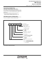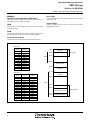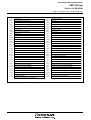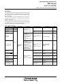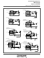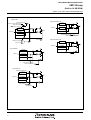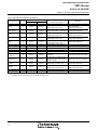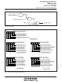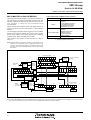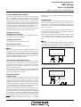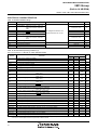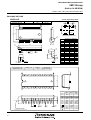
1
To all our customers
Regarding the change of names mentioned in the document, such as Mitsubishi
Electric and Mitsubishi XX, to Renesas Technology Corp.
The semiconductor operations of Hitachi and Mitsubishi Electric were transferred to Renesas
Technology Corporation on April 1st 2003. These operations include microcomputer, logic, analog
and discrete devices, and memory chips other than DRAMs (flash memory, SRAMs etc.)
Accordingly, although Mitsubishi Electric, Mitsubishi Electric Corporation, Mitsubishi
Semiconductors, and other Mitsubishi brand names are mentioned in the document, these names
have in fact all been changed to Renesas Technology Corp. Thank you for your understanding.
Except for our corporate trademark, logo and corporate statement, no changes whatsoever have been
made to the contents of the document, and these changes do not constitute any alteration to the
contents of the document itself.
Note : Mitsubishi Electric will continue the business operations of high frequency & optical devices
and power devices.
Renesas Technology Corp.
Customer Support Dept.
April 1, 2003
MITSUBISHI MICROCOMPUTERS
3851 Group
(Built-in 16 KB ROM)
✽This data sheet explains the products which have
16 KB ROM.
DESCRIPTION
The 3851 group is the 8-bit microcomputer based on the 740 family core technology.
The 3851 group is designed for the household products and office
automation equipment and includes serial I/O functions, 8-bit
timer, A-D converter, and I2C-bus interface.
FEATURES
●Basic machine-language instructions ...................................... 71
●Minimum instruction execution time .................................. 0.5 µs
(at 8 MHz oscillation frequency)
●Memory size
ROM ............................................................................. 16 Kbytes
RAM .............................................................................. 512 bytes
●Programmable input/output ports ............................................ 34
●Interrupts ................................................. 16 sources, 16 vectors
●Timers ............................................................................. 8-bit ✕ 4
●Serial I/O ....................... 8-bit ✕ 1(UART or Clock-synchronized)
●Multi-master I2C-bus interface (option) ....................... 1 channel
●PWM ............................................................................... 8-bit ✕ 1
●A-D converter ............................................... 10-bit ✕ 5 channels
●Watchdog timer ............................................................ 16-bit ✕ 1
●Clock generating circuit ..................................... Built-in 2 circuits
(connect to external ceramic resonator or quartz-crystal oscillator)
SINGLE-CHIP 8-BIT CMOS MICROCOMPUTER
●Power source voltage
In high-speed mode .................................................. 4.0 to 5.5 V
(at 8 MHz oscillation frequency)
In high-speed mode .................................................. 2.7 to 5.5 V
(at 4 MHz oscillation frequency)
In middle-speed mode ............................................... 2.7 to 5.5 V
(at 8 MHz oscillation frequency)
In low-speed mode .................................................... 2.7 to 5.5 V
(at 32 kHz oscillation frequency)
●Power dissipation
In high-speed mode .......................................................... 34 mW
(at 8 MHz oscillation frequency, at 5 V power source voltage)
In low-speed mode ............................................................ 60 µW
(at 32 kHz oscillation frequency, at 3 V power source voltage)
●Operating temperature range .................................... –20 to 85°C
APPLICATION
Office automation equipment, FA equipment, Household products,
Consumer electronics, etc.
PIN CONFIGURATION (TOP VIEW)
1
42
2
41
3
40
4
39
5
38
6
37
7
8
9
10
11
12
13
14
15
16
M38513M4-XXXFP
M38513M4-XXXSP
VCC
VREF
AVSS
P44/INT3/PWM
P43/INT2
P42/INT1
P41/INT0
P40/CNTR1
P27/CNTR0/SRDY
P26/SCLK
P25/SCL2/TxD
P24/SDA2/RxD
P23/SCL1
P22/SDA1
CNVSS
P21/XCIN
P20/XCOUT
RESET
XIN
XOUT
VSS
36
35
34
33
32
31
30
29
28
27
17
26
18
25
19
24
20
23
21
22
P30/AN0
P31/AN1
P32/AN2
P33/AN3
P34/AN4
P00
P01
P02
P03
P04
P05
P06
P07
P10
P11
P12
P13/(LED0)
P14/(LED1)
P15/(LED2)
P16/(LED3)
P17/(LED4)
Package type : FP ........................... 42P2R-A/E (42-pin plastic-molded SSOP)
Package type : SP ........................... 42P4B (42-pin shrink plastic-molded DIP)
Fig. 1 M38513M4-XXXFP/SP pin configuration
2
Fig. 2 Functional block diagram
Sub-clock Sub-clock
input
output
XCIN XCOUT
3
AVSS
VREF
2
A-D
converter
(10)
PWM
(8)
Reset
Clock generating circuit
20
Main-clock
output
XOUT
Watchdog
timer
19
Main-clock
input
XIN
I/O port P4
4 5 6 7 8
P4(5)
RAM
FUNCTIONAL BLOCK DIAGRAM
INT0–
INT3
ROM
I/O port P3
38 39 40 41 42
P3(5)
21
VSS
PC H
A
SI/O(8)
PS
2
I C
PC L
S
Y
X
18
C P U
RESET
1
CNTR0
Reset input
VCC
P2(8)
CNTR1
I/O port P2
XCOUT
XCIN
Prescaler Y(8)
Prescaler X(8)
Prescaler 12(8)
9 10 11 12 13 14 16 17
15
CNVSS
I/O port P1
22 23 24 25 26 27 28 29
P1(8)
P0(8)
I/O port P0
30 31 32 3334 35 36 37
Timer Y( 8 )
Timer X( 8 )
Timer 2( 8 )
Timer 1( 8 )
MITSUBISHI MICROCOMPUTERS
3851 Group
(Built-in 16 KB ROM)
SINGLE-CHIP 8-BIT CMOS MICROCOMPUTER
FUNCTIONAL BLOCK
MITSUBISHI MICROCOMPUTERS
3851 Group
(Built-in 16 KB ROM)
SINGLE-CHIP 8-BIT CMOS MICROCOMPUTER
PIN DESCRIPTION
Table 1 Pin description
Pin
Functions
Name
VCC, VSS
CNVSS
Power source
CNVSS input
•Apply voltage of 2.7 V – 5.5 V to Vcc, and 0 V to Vss.
VREF
Reference
voltage input
Analog power
source input
Reset input
Clock input
•Reference voltage input pin for A-D converter.
Function except a port function
•This pin controls the operation mode of the chip.
•Normally connected to VSS.
AVss
RESET
XIN
XOUT
Clock output
P00–P07
I/O port P0
•Analog power source input pin for A-D converter.
•Connect to Vss.
•Reset input pin for active “L.”
•Input and output pins for the clock generating circuit.
•Connect a ceramic resonator or quartz-crystal oscillator between the XIN and XOUT pins to set
the oscillation frequency.
•When an external clock is used, connect the clock source to the XIN pin and leave the XOUT
pin open.
•8-bit CMOS I/O port.
•I/O direction register allows each pin to be individually programmed as either input or output.
•CMOS compatible input level.
P10–P17
I/O port P1
P20/XCOUT
P21/XCIN
P22/SDA1
P23/SCL1
P24/SDA2/RxD
P25/SCL2/TxD
P26/SCLK
P27/CNTR0/
SRDY
I/O port P2
P30/AN0–
P34/AN4
I/O port P3
P40/CNTR1
P41/INT0–
P43/INT2
P44/INT3/PWM
I/O port P4
•CMOS 3-state output structure.
•P13 to P17 (5 bits) are enabled to output large current for LED drive.
•8-bit CMOS I/O port.
• Sub-clock generating circuit I/O
pins (connect a resonator)
•I/O direction register allows each pin to be individually
programmed as either input or output.
• I2C-BUS interface function pins
•CMOS compatible input level.
•P22 to P25 can be switched between CMOS compatible input level or SMBUS input level in the I2C-BUS
interface function.
•P20, P21, P24 to P27: CMOS3-state output structure.
•P24, P25: N-channel open-drain structure in the I2CBUS interface function.
• I2C-BUS interface function pin/
Serial I/O function pins
• Serial I/O function pin
• Serial I/O function pin/
Timer X function pin
•P22, P23: N-channel open-drain structure.
•8-bit CMOS I/O port with the same function as port P0.
• A-D converter input pin
•CMOS compatible input level.
•CMOS 3-state output structure.
•8-bit CMOS I/O port with the same function as port P0.
•CMOS compatible input level.
• Timer Y function pin
• Interrupt input pins
•CMOS 3-state output structure.
• Interrupt input pin
• PWM output pin
3
MITSUBISHI MICROCOMPUTERS
3851 Group
(Built-in 16 KB ROM)
SINGLE-CHIP 8-BIT CMOS MICROCOMPUTER
GROUP EXPANSION
Packages
Mitsubishi plans to expand the 3851 group as follows:
42P2R-A ............................................ 42-pin plastic molded SSOP
42P4B ......................................... 42-pin shrink plastic-molded DIP
Memory Type
Support for mask ROM and One Time PROM versions.
Memory Size
ROM/PROM size ............................................................ 16 K bytes
RAM size ......................................................................... 512 bytes
Memory Expansion Plan
ROM size (bytes)
48K
32K
28K
24K
20K
Mass production
M38513E4FP/SP
M38513M4-XXXFP/SP
16K
12K
8K
128
192
256
384
512
RAM size (bytes)
Fig. 3 Memory expansion plan
4
640
768
896
1024
MITSUBISHI MICROCOMPUTERS
3851 Group
(Built-in 16 KB ROM)
SINGLE-CHIP 8-BIT CMOS MICROCOMPUTER
FUNCTIONAL DESCRIPTION
CENTRAL PROCESSING UNIT (CPU)
The 3851 group uses the standard 740 Family instruction set. Refer to the table of 740 Family addressing modes and machine
instructions or the 740 Family Software Manual for details on the
instruction set.
Machine-resident 740 Family instructions are as follows:
The FST and SLW instructions cannot be used.
The STP, WIT, MUL, and DIV instructions can be used.
[CPU Mode Register (CPUM)] 003B16
The CPU mode register contains the stack page selection bit, etc.
The CPU mode register is allocated at address 003B16.
b7
b0
CPU mode register
(CPUM : address 003B16)
Processor mode bits
b1 b0
0 0 : Single-chip mode
0 1 :
1 0 : Not available
1 1 :
Stack page selection bit
0 : 0 page
1 : 1 page
Not used (return “1” when read)
(Do not write “0” to this bit.)
Port X C switch bit
0 : I/O port function (stop oscillating)
1 : X CIN–XCOUT oscillating function
Main clock (X IN–XOUT ) stop bit
0 : Oscillating
1 : Stopped
Main clock division ratio selection bits
b7 b6
0 0 : φ = f(X IN)/2 (high-speed mode)
0 1 : φ = f(X IN)/8 (middle-speed mode)
1 0 : φ = f(X CIN)/2 (low-speed mode)
1 1 : Not available
Fig. 4 Structure of CPU mode register
5
MITSUBISHI MICROCOMPUTERS
3851 Group
(Built-in 16 KB ROM)
SINGLE-CHIP 8-BIT CMOS MICROCOMPUTER
MEMORY
Special Function Register (SFR) Area
The Special Function Register area in the zero page contains control registers such as I/O ports and timers.
Zero Page
Access to this area with only 2 bytes is possible in the zero page
addressing mode.
Special Page
RAM
RAM is used for data storage and for stack area of subroutine
calls and interrupts.
Access to this area with only 2 bytes is possible in the special
page addressing mode.
ROM
The first 128 bytes and the last 2 bytes of ROM are reserved for
device testing and the rest is user area for storing programs.
Interrupt Vector Area
The interrupt vector area contains reset and interrupt vectors.
RAM area
RAM size
(bytes)
Address
XXXX16
192
256
384
512
640
768
896
1024
1536
2048
3072
4032
00FF16
013F16
01BF16
023F16
02BF16
033F16
03BF16
043F16
063F16
083F16
0C3F16
0FFF16
000016
SFR area
RAM
010016
XXXX16
Reserved area
044016
Not used
YYYY16
ROM area
Reserved ROM area
ROM size
(bytes)
Address
YYYY16
Address
ZZZZ16
4096
8192
12288
16384
20480
24576
28672
32768
36864
40960
45056
49152
53248
57344
61440
F00016
E00016
D00016
C00016
B00016
A00016
900016
800016
700016
600016
500016
400016
300016
200016
100016
F08016
E08016
D08016
C08016
B08016
A08016
908016
808016
708016
608016
508016
408016
308016
208016
108016
Fig. 5 Memory map diagram
6
Zero page
004016
(128 bytes)
ZZZZ16
ROM
FF0016
FFDC16
Interrupt vector area
FFFE16
FFFF16
Reserved ROM area
Special page
MITSUBISHI MICROCOMPUTERS
3851 Group
(Built-in 16 KB ROM)
SINGLE-CHIP 8-BIT CMOS MICROCOMPUTER
000016
Port P0 (P0)
002016
Prescaler 12 (PRE12)
000116
Port P0 direction register (P0D)
002116
Timer 1 (T1)
000216
Port P1 (P1)
002216
Timer 2 (T2)
000316
Port P1 direction register (P1D)
002316
Timer XY mode register (TM)
000416
Port P2 (P2)
002416
Prescaler X (PREX)
000516
Port P2 direction register (P2D)
002516
Timer X (TX)
000616
Port P3 (P3)
002616
Prescaler Y (PREY)
000716
Port P3 direction register (P3D)
002716
Timer Y (TY)
000816
Port P4 (P4)
002816
Timer count source selection register (TCSS)
000916
Port P4 direction register (P4D)
002916
000A16
002A16
000B16
002B16
I2C data shift register (S0)
000C16
002C16
I2C address register (S0D)
000D16
002D16
I2C status register (S1)
000E16
002E16
I2C control register (S1D)
000F16
002F16
I2C clock control register (S2)
001016
003016
001116
003116
I2C start/stop condition control register (S2D)
Reserved ✽
001216
003216
001316
003316
001416
003416
A-D control register (ADCON)
A-D conversion low-order register (ADL)
A-D conversion high-order register (ADH)
001516
Reserved ✽
003516
001616
Reserved ✽
003616
001716
Reserved ✽
003716
001816
Transmit/Receive buffer register (TB/RB)
003816
MISRG
001916
Serial I/O status register (SIOSTS)
003916
Watchdog timer control register (WDTCON)
001A16
Serial I/O control register (SIOCON)
003A16
Interrupt edge selection register (INTEDGE)
001B16
UART control register (UARTCON)
003B16
CPU mode register (CPUM)
001C16
Baud rate generator (BRG)
003C16
Interrupt request register 1 (IREQ1)
001D16
PWM control register (PWMCON)
003D16
Interrupt request register 2 (IREQ2)
001E16
PWM prescaler (PREPWM)
003E16
Interrupt control register 1 (ICON1)
001F16
PWM register (PWM)
003F16
Interrupt control register 2 (ICON2)
✽ Reserved : Do not write “1” to this address.
Fig. 6 Memory map of special function register (SFR)
7
MITSUBISHI MICROCOMPUTERS
3851 Group
(Built-in 16 KB ROM)
SINGLE-CHIP 8-BIT CMOS MICROCOMPUTER
I/O PORTS
The I/O ports have direction registers which determine the input/
output direction of each individual pin. Each bit in a direction register corresponds to one pin, and each pin can be set to be input
port or output port.
When “0” is written to the bit corresponding to a pin, that pin becomes an input pin. When “1” is written to that bit, that pin
becomes an output pin.
If data is read from a pin which is set to output, the value of the
port output latch is read, not the value of the pin itself. Pins set to
input are floating. If a pin set to input is written to, only the port
output latch is written to and the pin remains floating.
Table 2 I/O port function
Pin
Name
P00–P07
Port P0
P10–P17
Port P1
Input/Output
CMOS compatible
input level
CMOS 3-state output
P20/XCOUT
P21/XCIN
Non-Port Function
Related SFRs
Ref.No.
(1)
(2)
Sub-clock generating
circuit
CPU mode register
I2C-BUS interface function I/O
I2C control register
(4)
(5)
(6)
(7)
Serial I/O function I/O
I2C control register
Serial I/O control
register
P26/SCLK
Serial I/O function I/O
Serial I/O control
register
(8)
P27/CNTR0/SRDY
Serial I/O function I/O
Timer X function I/O
Serial I/O control
register
Timer XY mode register
(9)
A-D conversion input
A-D control register
(10)
Timer Y function I/O
Timer XY mode register
(11)
External interrupt input
Interrupt edge selection
register
(12)
Interrupt edge selection
register
PWM control register
(13)
P22/SDA1
P23/SCL1
Port P2
P24/SDA2/RxD
P25/SCL2/TxD
P30/AN0—
P34/AN4
Input/output,
individual
bits
Port P3
P40/CNTR1
P41/INT0—
P43/INT2
P44/INT3/PWM
8
I/O Structure
CMOS compatible
input level
CMOS/SMBUS input
level (when selecting
I2C-BUS interface
function)
N-channel open-drain
output
CMOS compatible
input level
CMOS/SMBUS input
level (when selecting
I2C-BUS interface
function)
CMOS 3-state output
N-channel open-drain
output (when
selecting I2C-BUS
interface function)
CMOS compatible
input level
CMOS 3-state output
I2C-BUS interface function I/O
Port P4
External interrupt input
PWM output
(3)
MITSUBISHI MICROCOMPUTERS
3851 Group
(Built-in 16 KB ROM)
SINGLE-CHIP 8-BIT CMOS MICROCOMPUTER
(2) Port P20
(1) Ports P0, P1
Port XC switch bit
Direction
register
Data bus
Direction
register
Port latch
Data bus
Port latch
Oscillator
Port P21
(3) Port P21
Port XC switch bit
Port XC switch bit
Direction
register
(4) Port P22
I2 C-BUS interface enable bit
SDA/SCL pin selection bit
Data bus
Port latch
Direction
register
Data bus
Port latch
Sub-clock generating circuit input
SDA output
(5) Port P23
SDA input
I2 C-BUS interface enable bit
SDA/SCL pin selection bit
(6) Port P24
Direction
register
Data bus
I2 C-BUS interface enable bit
SDA/SCL pin selection bit
Serial I/O enable bit
Receive enable bit
Port latch
Direction
register
Data bus
Port latch
SCL output
SCL input
(7) Port P25
SDA output
P-channel output disable bit
SDA input
Serial I/O input
Serial I/O enable bit
Transmit enable bit
2
I C bus interface enable bit
SDA/SCL pin selection bit
(8) Port P26
Serial I/O enable bit
Serial I/O clock selection bit
Direction
register
Serial I/O mode selection bit
Data bus
Port latch
Serial I/O enable bit
Direction
register
Data bus
Port latch
SCL input
Serial I/O output
SCL output
Serial clock output
External clock input
Fig. 7 Port block diagram (1)
9
MITSUBISHI MICROCOMPUTERS
3851 Group
(Built-in 16 KB ROM)
SINGLE-CHIP 8-BIT CMOS MICROCOMPUTER
(9) Port P27
(10) Ports P30–P34
Pulse output mode
Serial I/O mode selection bit
Serial I/O enable bit
SRDY output enable bit
Direction
register
Data bus
Direction
register
Data bus
Port latch
Port latch
A-D converter input
Analog input pin selection bit
Pulse output mode
CNTR0 interrupt
input
Serial ready output
(12) Ports P41–P43
Direction
register
Timer output
Data bus
Port latch
(11) Port P40
Direction
register
Interrupt input
Data bus
Port latch
Pulse output mode
Timer output
CNTR1 interrupt input
(13) Port P44
PWM output enable bit
Direction
register
Data bus
Port latch
PWM output
Interrupt input
Fig. 8 Port block diagram (2)
10
MITSUBISHI MICROCOMPUTERS
3851 Group
(Built-in 16 KB ROM)
SINGLE-CHIP 8-BIT CMOS MICROCOMPUTER
INTERRUPTS
■Notes
Interrupts occur by 16 sources among 16 sources: seven external,
eight internal, and one software.
When setting the followings, the interrupt request bit may be set to
“1”.
•When setting external interrupt active edge
Related register: Interrupt edge selection register (address 3A16)
Timer XY mode register (address 2316)
•When switching interrupt sources of an interrupt vector address
where two or more interrupt sources are allocated
Related register: Interrupt edge selection register (address 3A16)
When not requiring for the interrupt occurrence synchronized with
these setting, take the following sequence.
➀Set the corresponding interrupt enable bit to “0” (disabled).
➁Set the interrupt edge select bit or the interrupt source select bit.
➂Set the corresponding interrupt request bit to “0” after 1 or more
instructions have been executed.
➃Set the corresponding interrupt enable bit to “1” (enabled).
Interrupt Control
Each interrupt is controlled by an interrupt request bit, an interrupt
enable bit, and the interrupt disable flag except for the software interrupt set by the BRK instruction. An interrupt occurs if the
corresponding interrupt request and enable bits are “1” and the interrupt disable flag is “0”.
Interrupt enable bits can be set or cleared by software.
Interrupt request bits can be cleared by software, but cannot be
set by software.
The BRK instruction cannot be disabled with any flag or bit. The I
(interrupt disable) flag disables all interrupts except the BRK instruction interrupt.
When several interrupts occur at the same time, the interrupts are
received according to priority.
Interrupt Operation
By acceptance of an interrupt, the following operations are automatically performed:
1. The contents of the program counter and the processor status
register are automatically pushed onto the stack.
2. The interrupt disable flag is set and the corresponding interrupt
request bit is cleared.
3. The interrupt jump destination address is read from the vector
table into the program counter.
11
MITSUBISHI MICROCOMPUTERS
3851 Group
(Built-in 16 KB ROM)
SINGLE-CHIP 8-BIT CMOS MICROCOMPUTER
Table 3 Interrupt vector addresses and priority
Interrupt Source
Reset (Note 2)
Priority
1
Vector Addresses (Note 1)
High
Low
FFFD16
FFFC16
Interrupt Request
Generating Conditions
Remarks
At reset
Non-maskable
External interrupt
(active edge selectable)
INT0
2
FFFB16
FFFA16
At detection of either rising or
falling edge of INT0 input
SCL, SDA
3
FFF916
FFF816
At detection of either rising or
falling edge of SCL or SDA input
External interrupt
(active edge selectable)
INT1
4
FFF716
FFF616
At detection of either rising or
falling edge of INT1 input
External interrupt
(active edge selectable)
INT2
5
FFF516
FFF416
At detection of either rising or
falling edge of INT2 input
External interrupt
(active edge selectable)
INT3
6
FFF316
FFF216
At detection of either rising or
falling edge of INT3 input
External interrupt
(active edge selectable)
I 2C
Timer X
Timer Y
Timer 1
7
8
FFF116
FFF016
At completion of data transfer
FFEF16
9
FFED16
10
11
FFEB16
FFE916
FFEE16
FFEC16
FFEA16
At timer X underflow
At timer Y underflow
At timer 1 underflow
FFE816
At timer 2 underflow
Serial I/O
reception
12
FFE716
FFE616
At completion of serial I/O data
reception
Valid when serial I/O is selected
Serial I/O
Transmission
13
FFE516
FFE416
At completion of serial I/O transfer shift or when transmission
buffer is empty
Valid when serial I/O is selected
CNTR0
14
FFE316
FFE216
At detection of either rising or
falling edge of CNTR0 input
External interrupt
(active edge selectable)
CNTR1
15
FFE116
FFE016
At detection of either rising or
falling edge of CNTR1 input
External interrupt
(active edge selectable)
A-D converter
BRK instruction
16
FFDF16
FFDE16
At completion of A-D conversion
17
FFDD16
FFDC16
At BRK instruction execution
Timer 2
Notes 1: Vector addresses contain interrupt jump destination addresses.
2: Reset function in the same way as an interrupt with the highest priority.
12
STP release timer underflow
Non-maskable software interrupt
MITSUBISHI MICROCOMPUTERS
3851 Group
(Built-in 16 KB ROM)
SINGLE-CHIP 8-BIT CMOS MICROCOMPUTER
Interrupt request bit
Interrupt enable bit
Interrupt disable flag (I)
BRK instruction
Reset
Interrupt request
Fig. 9 Interrupt control
b7
b0 Interrupt edge selection register
(INTEDGE : address 003A16)
INT0 active edge selection bit
INT1 active edge selection bit
INT2 active edge selection bit
INT3 active edge selection bit
Reserved (Do not write “1” to this bit.)
Not used (returns “0” when read)
0 : Falling edge active
1 : Rising edge active
b7
b0 Interrupt request register 1
(IREQ1 : address 003C16)
b7
b0 Interrupt request register 2
(IREQ2 : address 003D16)
INT0 interrupt request bit
SCL/SDA interrupt request bit
INT1 interrupt request bit
INT2 interrupt request bit
INT3 interrupt request bit
I2C interrupt request bit
Timer X interrupt request bit
Timer Y interrupt request bit
Timer 1 interrupt request bit
Timer 2 interrupt request bit
Serial I/O reception interrupt request bit
Serial I/O transmit interrupt request bit
CNTR0 interrupt request bit
CNTR1 interrupt request bit
AD converter interrupt request bit
Not used (returns “0” when read)
0 : No interrupt request issued
1 : Interrupt request issued
0 : No interrupt request issued
1 : Interrupt request issued
b7
b0
Interrupt control register 1
(ICON1 : address 003E16)
INT0 interrupt enable bit
SCL/SDA interrupt enable bit
INT1 interrupt enable bit
INT2 interrupt enable bit
INT3 interrupt enable bit
I2C interrupt enable bit
Timer X interrupt enable bit
Timer Y interrupt enable bit
0 : Interrupts disabled
1 : Interrupts enabled
b7
b0
Interrupt control register 2
(ICON2 : address 003F16)
Timer 1 interrupt enable bit
Timer 2 interrupt enable bit
Serial I/O reception interrupt enable bit
Serial I/O transmit interrupt enable bit
CNTR0 interrupt enable bit
CNTR1 interrupt enable bit
AD converter interrupt enable bit
Not used (returns “0” when read)
(Do not write “1” to this bit)
0 : Interrupts disabled
1 : Interrupts enabled
Fig. 10 Structure of interrupt-related registers (1)
13
MITSUBISHI MICROCOMPUTERS
3851 Group
(Built-in 16 KB ROM)
SINGLE-CHIP 8-BIT CMOS MICROCOMPUTER
TIMERS
Timer 1 and Timer 2
The 3851 group has four timers: timer X, timer Y, timer 1, and
timer 2.
The division ratio of each timer or prescaler is given by 1/(n + 1),
where n is the value in the corresponding timer or prescaler latch.
All timers are count down. When the timer reaches “0016”, an underflow occurs at the next count pulse and the corresponding
timer latch is reloaded into the timer and the count is continued.
When a timer underflows, the interrupt request bit corresponding
to that timer is set to “1”.
The count source of prescaler 12 is the oscillation frequency divided by 16. The output of prescaler 12 is counted by timer 1 and
timer 2, and a timer underflow sets the interrupt request bit.
Timer X and Timer Y
Timer X and Timer Y can each select in one of four operating
modes by setting the timer XY mode register.
(1) Timer Mode
The timer counts the count source selected by Timer count source
selection bit.
(2) Pulse Output Mode
b0
b7
Timer XY mode register
(TM : address 002316)
Timer X operating mode bits
b1b0
0 0: Timer mode
0 1: Pulse output mode
1 0: Event counter mode
1 1: Pulse width measurement mode
CNTR0 active edge selection bit
0: Interrupt at falling edge
Count at rising edge in event
counter mode
1: Interrupt at rising edge
Count at falling edge in event
counter mode
Timer X count stop bit
0: Count start
1: Count stop
Timer Y operating mode bit
b5b4
0 0: Timer mode
0 1: Pulse output mode
1 0: Event counter mode
1 1: Pulse width measurement mode
CNTR1 active edge selection bit
0: Interrupt at falling edge
Count at rising edge in event
counter mode
1: Interrupt at rising edge
Count at falling edge in event
counter mode
Timer Y count stop bit
0: Count start
1: Count stop
The timer counts the count source selected by Timer count source
selection bit. Whenever the contents of the timer reach “0016”, the
signal output from the CNTR0 (or CNTR1) pin is inverted. If the
CNTR0 (or CNTR1) active edge selection bit is “0”, output begins
at “ H”.
If it is “1”, output starts at “L”. When using a timer in this mode, set
the corresponding port P27 ( or port P40) direction register to output mode.
(3) Event Counter Mode
Operation in event counter mode is the same as in timer mode, except that the timer counts signals input through the CNTR 0 or
CNTR1 pin.
When the CNTR0 (or CNTR1) active edge selection bit is “0”, the
rising edge of the CNTR0 (or CNTR1) pin is counted.
When the CNTR0 (or CNTR1) active edge selection bit is “1”, the
falling edge of the CNTR0 (or CNTR1) pin is counted.
(4) Pulse Width Measurement Mode
If the CNTR0 (or CNTR1) active edge selection bit is “0”, the timer
counts the selected signals by the count source selection bit while
the CNTR0 (or CNTR1) pin is at “H”. If the CNTR0 (or CNTR1) active edge selection bit is “1”, the timer counts it while the CNTR0
(or CNTR1) pin is at “L”.
Fig. 11 Structure of timer XY mode register
b7
b0
Timer count source selection register
(TCSS : address 002816)
Timer X count source selection bit
0 : f(XIN)/16 (f(XCIN)/16 at low-speed mode)
1 : f(XIN)/2 (f(XCIN)/2 at low-speed mode)
Timer Y count source selection bit
0 : f(XIN)/16 (f(XCIN)/16 at low-speed mode)
1 : f(XIN)/2 (f(XCIN)/2 at low-speed mode)
Timer 12 count source selection bit
0 : f(XIN)/16 (f(XCIN)/16 at low-speed mode)
1 : f(XCIN)
Not used (returns “0” when read)
Fig. 12 Structure of timer count source selection register
14
The count can be stopped by setting “1” to the timer X (or timer Y)
count stop bit in any mode. The corresponding interrupt request
bit is set each time a timer overflows.
■Note
When switching the count source by the timer 12, X and Y count
source bit, the value of timer count is altered in unconsiderable
amount owing to generating of a thin pulses in the count input
signals.
Therefore, select the timer count source before set the value to
the prescaler and the timer.
MITSUBISHI MICROCOMPUTERS
3851 Group
(Built-in 16 KB ROM)
SINGLE-CHIP 8-BIT CMOS MICROCOMPUTER
Data bus
f(XIN)/16
f(XIN)/2
Prescaler X latch (8)
Timer X latch (8)
Pulse width
Timer X count source selection bit measurement Timer mode
Pulse output mode
mode
Prescaler X (8)
CNTR0 active
edge selection
bit
“0”
P27/CNTR0
Event
counter
mode
“1”
Timer X (8)
Timer X count stop bit
To CNTR0 interrupt
request bit
CNTR0 active
edge selection “1”
bit
“0”
Q
Toggle flip-flop T
Q
R
Timer X latch write pulse
Pulse output mode
Port P27
latch
Port P27
direction register
To timer X interrupt
request bit
Pulse output mode
Data bus
Prescaler Y latch (8)
f(XIN)/16
f(XIN)/2
Timer Y count source selection bit
Pulse width
measurement mode
Timer mode
Pulse output mode
Prescaler Y (8)
CNTR1 active
edge selection
bit
“0”
P40/CNTR1
Event
counter
mode
“1”
Port P40
direction register
Timer Y (8)
To timer Y interrupt
request bit
Timer Y count stop bit
To CNTR1 interrupt
request bit
CNTR1 active
edge selection “1”
bit
Q
Toggle flip-flop T
Q
Port P40
latch
Timer Y latch (8)
“0”
R
Timer Y latch write pulse
Pulse output mode
Pulse output mode
Data bus
Prescaler 12 latch (8)
f(XIN)/16
f(XCIN)
Prescaler 12 (8)
Timer 1 latch (8)
Timer 2 latch (8)
Timer 1 (8)
Timer 2 (8)
To timer 2 interrupt
request bit
Timer 12 count source selection bit
To timer 1 interrupt
request bit
Fig. 13 Block diagram of timer X, timer Y, timer 1, and timer 2
15
MITSUBISHI MICROCOMPUTERS
3851 Group
(Built-in 16 KB ROM)
SINGLE-CHIP 8-BIT CMOS MICROCOMPUTER
SERIAL I/O
(1) Clock Synchronous Serial I/O Mode
Serial I/O can be used as either clock synchronous or asynchronous (UART) serial I/O. A dedicated timer is also provided for baud
rate generation.
Clock synchronous serial I/O mode can be selected by setting the
serial I/O mode selection bit of the serial I/O control register (bit 6
of address 001A16) to “1”.
For clock synchronous serial I/O, the transmitter and the receiver
must use the same clock. If an internal clock is used, transfer is
started by a write signal to the TB/RB.
Data bus
Serial I/O control register
Address 001816
Receive buffer register
Receive interrupt request (RI)
Receive shift register
P24/RXD
Address 001A16
Receive buffer full flag (RBF)
Shift clock
Clock control circuit
P26/SCLK
XIN
Serial I/O synchronous
clock selection bit
Frequency division ratio 1/(n+1)
BRG count source selection bit
Baud rate generator
Address 001C16
1/4
P27/SRDY
F/F
1/4
Clock control circuit
Falling-edge detector
Shift clock
P25/TXD
Transmit shift register
Transmit shift completion flag (TSC)
Transmit interrupt source selection bit
Transmit interrupt request (TI)
Transmit buffer register
Transmit buffer empty flag (TBE)
Serial I/O status register
Address 001916
Address 001816
Data bus
Fig. 14 Block diagram of clock synchronous serial I/O
Transfer shift clock
(1/2 to 1/2048 of the internal
clock, or an external clock)
Serial output TxD
D0
D1
D2
D3
D4
D5
D6
D7
Serial input RxD
D0
D1
D2
D3
D4
D5
D6
D7
Receive enable signal SRDY
Write pulse to receive/transmit
buffer register (address 001816)
TBE = 0
TBE = 1
TSC = 0
RBF = 1
TSC = 1
Overrun error (OE)
detection
Notes 1: As the transmit interrupt (TI), either when the transmit buffer has emptied (TBE=1) or after the transmit shift operation has
ended (TSC=1), by setting the transmit interrupt source selection bit (TIC) of the serial I/O control register.
2: If data is written to the transmit buffer register when TSC=0, the transmit clock is generated continuously and serial data
is output continuously from the TxD pin.
3: The receive interrupt (RI) is set when the receive buffer full flag (RBF) becomes “1” .
Fig. 15 Operation of clock synchronous serial I/O function
16
MITSUBISHI MICROCOMPUTERS
3851 Group
(Built-in 16 KB ROM)
SINGLE-CHIP 8-BIT CMOS MICROCOMPUTER
(2) Asynchronous Serial I/O (UART) Mode
two buffers have the same address in memory. Since the shift register cannot be written to or read from directly, transmit data is
written to the transmit buffer register, and receive data is read from
the receive buffer register.
The transmit buffer register can also hold the next data to be
transmitted, and the receive buffer register can hold a character
while the next character is being received.
Clock asynchronous serial I/O mode (UART) can be selected by
clearing the serial I/O mode selection bit (b6) of the serial I/O control register to “0”.
Eight serial data transfer formats can be selected, and the transfer
formats used by a transmitter and receiver must be identical.
The transmit and receive shift registers each have a buffer, but the
Data bus
Address 0018 16
Serial I/O control register
P24/RXD
Address 001A16
Receive buffer full flag (RBF)
Receive interrupt request (RI)
Receive buffer register
OE
Character length selection bit
ST detector
7 bits
Receive shift register
1/16
8 bits
PE FE
SP detector
Clock control circuit
UART control register
Address 001B16
Serial I/O synchronous clock selection bit
P26/SCLK1
XIN
BRG count source selection bit Frequency division ratio 1/(n+1)
Baud rate generator
Address 001C 16
1/4
ST/SP/PA generator
1/16
P25/TXD
Transmit shift register
Transmit shift completion flag (TSC)
Transmit interrupt source selection bit
Transmit interrupt request (TI)
Character length selection bit
Transmit buffer register
Address 001816
Transmit buffer empty flag (TBE)
Serial I/O status register Address 001916
Data bus
Fig.16 Block diagram of UART serial I/O
17
MITSUBISHI MICROCOMPUTERS
3851 Group
(Built-in 16 KB ROM)
SINGLE-CHIP 8-BIT CMOS MICROCOMPUTER
Transmit or receive clock
Transmit buffer write
signal
TBE=0
TSC=0
TBE=1
Serial output TXD
TBE=0
TBE=1
ST
D0
D1
SP
TSC=1
ST
D0
Receive buffer read
signal
SP
D1
1 start bit
7 or 8 data bit
1 or 0 parity bit
1 or 2 stop bit (s)
Generated at 2nd bit in 2-stop-bit mode
RBF=0
RBF=1
Serial input RXD
ST
D0
D1
SP
RBF=1
ST
D0
D1
SP
Notes 1: Error flag detection occurs at the same time that the RBF flag becomes “1” (at 1st stop bit, during reception).
2: As the transmit interrupt (TI), when either the TBE or TSC flag becomes “1,” can be selected to occur depending on the setting of the transmit
interrupt source selection bit (TIC) of the serial I/O control register.
3: The receive interrupt (RI) is set when the RBF flag becomes “1.”
4: After data is written to the transmit buffer when TSC=1, 0.5 to 1.5 cycles of the data shift cycle is necessary until changing to TSC=0.
Fig. 17 Operation of UART serial I/O function
[Transmit Buffer Register/Receive Buffer
Register (TB/RB)] 001816
The transmit buffer register and the receive buffer register are located at the same address. The transmit buffer is write-only and
the receive buffer is read-only. If a character bit length is 7 bits, the
MSB of data stored in the receive buffer is “0”.
[Serial I/O Status Register (SIOSTS)] 001916
The read-only serial I/O status register consists of seven flags
(bits 0 to 6) which indicate the operating status of the serial I/O
function and various errors.
Three of the flags (bits 4 to 6) are valid only in UART mode.
The receive buffer full flag (bit 1) is cleared to “0” when the receive
buffer register is read.
If there is an error, it is detected at the same time that data is
transferred from the receive shift register to the receive buffer register, and the receive buffer full flag is set. A write to the serial I/O
status register clears all the error flags OE, PE, FE, and SE (bit 3
to bit 6, respectively). Writing “0” to the serial I/O enable bit SIOE
(bit 7 of the serial I/O control register) also clears all the status
flags, including the error flags.
Bits 0 to 6 of the serial I/O status register are initialized to “0” at reset, but if the transmit enable bit (bit 4) of the serial I/O control
register has been set to “1”, the transmit shift completion flag (bit
2) and the transmit buffer empty flag (bit 0) become “1”.
18
[Serial I/O Control Register (SIOCON)] 001A16
The serial I/O control register consists of eight control bits for the
serial I/O function.
[UART Control Register (UARTCON)] 001B16
The UART control register consists of four control bits (bits 0 to 3)
which are valid when asynchronous serial I/O is selected and set
the data format of an data transfer and one bit (bit 4) which is always valid and sets the output structure of the P25/TXD pin.
[Baud Rate Generator (BRG)] 001C16
The baud rate generator determines the baud rate for serial transfer.
The baud rate generator divides the frequency of the count source
by 1/(n + 1), where n is the value written to the baud rate generator.
■Notes on Serial I/O
1. When using the serial I/O, clear the I2C-BUS interface enable
bit to “0” or the SCL/SDA interrupt pin selection bit to “0”.
2. When setting the transmit enable bit of serial I/O to “1”, the
serial I/O transmit interrupt request bit is automatically set to “1”.
When not requiring the interrupt occurrence synchronized with
the transmission enalbed, take the following sequence.
➀Set the serial I/O transmit interrupt enable bit to “0” (disabled).
➁Set the transmit enable bit to “1”.
➂Set the serial I/O transmit interrupt request bit to “0” after 1 or
more instructions have been executed.
➃Set the serial I/O transmit interrupt enable bit to “1” (enabled).
MITSUBISHI MICROCOMPUTERS
3851 Group
(Built-in 16 KB ROM)
SINGLE-CHIP 8-BIT CMOS MICROCOMPUTER
b7
b0
Serial I/O status register
(SIOSTS : address 0019 16)
Transmit buffer empty flag (TBE)
0: Buffer full
1: Buffer empty
Receive buffer full flag (RBF)
0: Buffer empty
1: Buffer full
Transmit shift completion flag (TSC)
0: Transmit shift in progress
1: Transmit shift completed
Overrun error flag (OE)
0: No error
1: Overrun error
Parity error flag (PE)
0: No error
1: Parity error
Framing error flag (FE)
0: No error
1: Framing error
Summing error flag (SE)
0: (OE) U (PE) U (FE)=0
1: (OE) U (PE) U (FE)=1
Not used (returns “1” when read)
b7
b0
UART control register
(UARTCON : address 001B 16)
Character length selection bit (CHAS)
0: 8 bits
1: 7 bits
b7
b0
Serial I/O control register
(SIOCON : address 001A 16)
BRG count source selection bit (CSS)
0: f(X IN)
1: f(X IN)/4
Serial I/O synchronous clock selection bit (SCS)
0: BRG output divided by 4 when clock synchronous
serial I/O is selected, BRG output divided by 16
when UART is selected.
1: External clock input when clock synchronous serial
I/O is selected, external clock input divided by 16
when UART is selected.
SRDY output enable bit (SRDY)
0: P2 7 pin operates as ordinary I/O pin
1: P2 7 pin operates as S RDY output pin
Transmit interrupt source selection bit (TIC)
0: Interrupt when transmit buffer has emptied
1: Interrupt when transmit shift operation is completed
Transmit enable bit (TE)
0: Transmit disabled
1: Transmit enabled
Receive enable bit (RE)
0: Receive disabled
1: Receive enabled
Serial I/O mode selection bit (SIOM)
0: Clock asynchronous (UART) serial I/O
1: Clock synchronous serial I/O
Serial I/O enable bit (SIOE)
0: Serial I/O disabled
(pins P2 4 to P2 7 operate as ordinary I/O pins)
1: Serial I/O enabled
(pins P2 4 to P2 7 operate as serial I/O pins)
Parity enable bit (PARE)
0: Parity checking disabled
1: Parity checking enabled
Parity selection bit (PARS)
0: Even parity
1: Odd parity
Stop bit length selection bit (STPS)
0: 1 stop bit
1: 2 stop bits
P25/TXD P-channel output disable bit (POFF)
0: CMOS output (in output mode)
1: N-channel open drain output (in output mode)
Not used (return “1” when read)
Fig. 18 Structure of serial I/O control registers
19
MITSUBISHI MICROCOMPUTERS
3851 Group
(Built-in 16 KB ROM)
SINGLE-CHIP 8-BIT CMOS MICROCOMPUTER
MULTI-MASTER I2C-BUS INTERFACE
Table 4 Multi-master I2C-BUS interface functions
The multi-master I2C-BUS interface is a serial communications circuit, conforming to the Philips I2C-BUS data transfer format. This
interface, offering both arbitration lost detection and a synchronous functions, is useful for the multi-master serial
communications.
Figure 19 shows a block diagram of the multi-master I2C-BUS interface and Table 4 lists the multi-master I 2 C-BUS interface
functions.
This multi-master I2C-BUS interface consists of the I2C address
register, the I 2C data shift register, the I2C clock control register,
the I2C control register, the I2C status register, the I2C start/stop
condition control register and other control circuits.
When using the multi-master I 2 C-BUS interface, set 1 MHz or
more to φ.
Item
Format
Communication mode
SCL clock frequency
Function
In conformity with Philips I2C-BUS
standard:
10-bit addressing format
7-bit addressing format
High-speed clock mode
Standard clock mode
In conformity with Philips I2C-BUS
standard:
Master transmission
Master reception
Slave transmission
Slave reception
16.1 kHz to 400 kHz (at φ= 4 MHz)
System clock φ = f(XIN)/2 (high-speed mode)
φ = f(XIN)/8 (middle-speed mode)
Note: Mitsubishi Electric Corporation assumes no responsibility for infringement of any third-party’s rights or originating in the use of the
connection control function between the I2C-BUS interface and the
ports SCL1, SCL2, SDA1 and SDA2 with the bit 6 of I2C control register (002E16).
b7
I2C address register
b0
Interrupt
generating
circuit
SAD6 SAD5 SAD4 SAD3 SAD2 SAD1 SA D0 RWB
S0D
Interrupt request signal
(IICIRQ)
Address comparator
Serial data
(SDA)
Noise
elimination
circuit
Data
control
circuit
b0
b7
I2C data shift register
b7
b0
S0
AL AAS AD0 LRB
MST TRX BB PIN
SIS SIP SSC4 SSC3 SSC2 SSC1 SSC0
S2D
AL
circuit
S1
I2C status register
I2C start/stop condition
control register
Internal data bus
BB
circuit
Serial
clock
(SCL)
Noise
elimination
circuit
Clock
control
circuit
b7
b0
FAST CCR4 CCR3 CCR2 CCR1 CCR0
ACK ACK MODE
BIT
S2
I2C clock control register
Clock division
I2C clock control register
S1D
b0
b7
TISS
CLK
STP
S1D
I 2C
System clock (φ)
10 BIT
S AD
ALS ES0 BC2 BC1 BC0
control register
Bit counter
Fig. 19 Block diagram of multi-master I2C-BUS interface
✽ : Purchase of MITSUBISHI ELECTRIC CORPORATIONS I2C components conveys a license under the Philips I2C Patent Rights to use these components
an I2C system, provided that the system conforms to the I2C Standard Specification as defined by Philips.
20
MITSUBISHI MICROCOMPUTERS
3851 Group
(Built-in 16 KB ROM)
SINGLE-CHIP 8-BIT CMOS MICROCOMPUTER
[I2C Data Shift Register (S0)] 002B16
The I2C data shift register (S0 : address 002B16) is an 8-bit shift
register to store receive data and write transmit data.
When transmit data is written into this register, it is transferred to
the outside from bit 7 in synchronization with the SCL clock, and
each time one-bit data is output, the data of this register are
shifted by one bit to the left. When data is received, it is input to
this register from bit 0 in synchronization with the SCL clock, and
each time one-bit data is input, the data of this register are shifted
by one bit to the left. The minimum 2 machine cycles are required
from the rising of the SCL clock until input to this register.
The I2C data shift register is in a write enable status only when the
I2C-BUS interface enable bit (ES0 bit : bit 3 of address 002E16) of
the I2C control register is “1”. The bit counter is reset by a write instruction to the I2C data shift register. When both the ES0 bit and
the MST bit of the I2C status register (address 002D16) are “1,” the
SCL is output by a write instruction to the I2C data shift register.
Reading data from the I2C data shift register is always enabled regardless of the ES0 bit value.
b7
b0
SAD6 SAD5 SAD4 SAD3 SAD2 SAD1 SAD0 RWB
I2C address register
(S0D: address 002C 16)
Read/write bit
Slave address
Fig. 20 Structure of I2C address register
[I2C Address Register (S0D)] 002C16
The I 2C address register (address 002C 16) consists of a 7-bit
slave address and a read/write bit. In the addressing mode, the
slave address written in this register is compared with the address
data to be received immediately after the START condition is detected.
•Bit 0: Read/write bit (RWB)
This is not used in the 7-bit addressing mode. In the 10-bit addressing mode, the first address data to be received is compared
with the contents (SAD6 to SAD0 + RWB) of the I2C address register.
The RWB bit is cleared to “0” automatically when the stop condition is detected.
•Bits 1 to 7: Slave address (SAD0–SAD6)
These bits store slave addresses. Regardless of the 7-bit addressing mode and the 10-bit addressing mode, the address data
transmitted from the master is compared with the contents of
these bits.
21
MITSUBISHI MICROCOMPUTERS
3851 Group
(Built-in 16 KB ROM)
SINGLE-CHIP 8-BIT CMOS MICROCOMPUTER
I2 C
Note: Do not write data into the
clock control register during transfer. If
data is written during transfer, the I 2C clock generator is reset, so
that data cannot be transferred normally.
22
I2C clock control register
(S2 : address 002F 16)
SCL frequency control bits
Refer to Table 5.
SCL mode specification bit
0 : Standard clock mode
1 : High-speed clock mode
ACK bit
0 : ACK is returned.
1 : ACK is not returned.
ACK clock bit
0 : No ACK clock
1 : ACK clock
Fig. 21 Structure of I2C clock control register
Table 5 Set values of I 2 C clock control register and SCL
frequency
Setting value of
CCR4–CCR0
CCR4 CCR3 CCR2 CCR1 CCR0
SCL frequency
(at φ = 4 MHz, unit : kHz)
Standard clock High-speed clock
mode
mode
0
0
0
0
Setting disabled
Setting disabled
0
0
0
0
1
Setting disabled
Setting disabled
0
0
0
1
0
Setting disabled
Setting disabled
0
0
0
1
1
– (Note 2)
333
0
0
1
0
0
– (Note 2)
250
0
0
1
0
1
100
400 (Note 3)
0
0
1
1
0
83.3
166
…
0
…
•Bit 7: ACK clock bit (ACK)
This bit specifies the mode of acknowledgment which is an acknowledgment response of data transfer. When this bit is set to
“0,” the no ACK clock mode is selected. In this case, no ACK clock
occurs after data transmission. When the bit is set to “1,” the ACK
clock mode is selected and the master generates an ACK clock
each completion of each 1-byte data transfer. The device for
transmitting address data and control data releases the SDA at
the occurrence of an ACK clock (makes SDA “H”) and receives the
ACK bit generated by the data receiving device.
b0
ACK FAST
CCR4 CCR3 CCR2 CCR1 CCR0
BIT MODE
…
✽ACK clock: Clock for acknowledgment
b7
ACK
…
The I2C clock control register (address 002F16) is used to set ACK
control, SCL mode and SCL frequency.
•Bits 0 to 4: SCL frequency control bits (CCR0–CCR4)
These bits control the SCL frequency. Refer to Table 5.
•Bit 5: SCL mode specification bit (FAST MODE)
This bit specifies the SCL mode. When this bit is set to “0,” the
standard clock mode is selected. When the bit is set to “1,” the
high-speed clock mode is selected.
When connecting the bus of the high-speed mode I2C bus standard (maximum 400 kbits/s), use 8 MHz or more oscillation
frequency f(XIN) and 2 division clock.
•Bit 6: ACK bit (ACK BIT)
This bit sets the SDA status when an ACK clock✽ is generated.
When this bit is set to “0,” the ACK return mode is selected and
SDA goes to “L” at the occurrence of an ACK clock. When the bit
is set to “1,” the ACK non-return mode is selected. The SDA is
held in the “H” status at the occurrence of an ACK clock.
However, when the slave address agree with the address data in
the reception of address data at ACK BIT = “0,” the SDA is automatically made “L” (ACK is returned). If there is a disagreement
between the slave address and the address data, the SDA is automatically made “H” (ACK is not returned).
…
[I2C Clock Control Register (S2)] 002F16
500/CCR value
(Note 3)
1
1
1
0
1
17.2
1000/CCR value
(Note 3)
34.5
1
1
1
1
0
16.6
33.3
1
1
1
1
1
16.1
32.3
Notes 1: Duty of SCL clock output is 50 %. The duty becomes 35 to 45 %
only when the high-speed clock mode is selected and CCR value
= 5 (400 kHz, at φ = 4 MHz). “H” duration of the clock fluctuates
from –4 to +2 machine cycles in the standard clock mode, and
fluctuates from –2 to +2 machine cycles in the high-speed clock
mode. In the case of negative fluctuation, the frequency does not
increase because “L” duration is extended instead of “H” duration
reduction.
These are value when SCL clock synchronization by the synchronous function is not performed. CCR value is the decimal
notation value of the SCL frequency control bits CCR4 to CCR0.
2: Each value of SCL frequency exceeds the limit at φ = 4 MHz or
more. When using these setting value, use φ of 4 MHz or less.
3: The data formula of SCL frequency is described below:
φ/(8 ✕ CCR value) Standard clock mode
φ/(4 ✕ CCR value) High-speed clock mode (CCR value ≠ 5)
φ/(2 ✕ CCR value) High-speed clock mode (CCR value = 5)
Do not set 0 to 2 as CCR value regardless of φ frequency.
Set 100 kHz (max.) in the standard clock mode and 400 kHz
(max.) in the high-speed clock mode to the SCL frequency by setting the SCL frequency control bits CCR4 to CCR0.
MITSUBISHI MICROCOMPUTERS
3851 Group
(Built-in 16 KB ROM)
SINGLE-CHIP 8-BIT CMOS MICROCOMPUTER
[I2C Control Register (S1D)] 002E16
The I2C control register (address 002E16) controls data communication format.
•Bits 0 to 2: Bit counter (BC0–BC2)
These bits decide the number of bits for the next 1-byte data to be
transmitted. The I2C interrupt request signal occurs immediately
after the number of count specified with these bits (ACK clock is
added to the number of count when ACK clock is selected by ACK
clock bit (bit 7 of address 002F 16)) have been transferred, and
BC0 to BC2 are returned to “0002”.
Also when a START condition is received, these bits become
“0002” and the address data is always transmitted and received in
8 bits.
•Bit 3: I2C interface enable bit (ES0)
This bit enables to use the multi-master I2C-BUS interface. When
this bit is set to “0,” the use disable status is provided, so that the
SDA and the SCL become high-impedance. When the bit is set to
“1,” use of the interface is enabled.
When ES0 = “0,” the following is performed.
• PIN = “1,” BB = “0” and AL = “0” are set (which are bits of the I2C
status register at address 002D16 ).
• Writing data to the I2C data shift register (address 002B16) is disabled.
•Bit 4: Data format selection bit (ALS)
This bit decides whether or not to recognize slave addresses.
When this bit is set to “0,” the addressing format is selected, so
that address data is recognized. When a match is found between a
slave address and address data as a result of comparison or when
a general call (refer to “I2 C Status Register,” bit 1) is received,
transfer processing can be performed. When this bit is set to “1,”
the free data format is selected, so that slave addresses are not
recognized.
•Bit 5: Addressing format selection bit (10BIT SAD)
This bit selects a slave address specification format. When this bit
is set to “0,” the 7-bit addressing format is selected. In this case,
only the high-order 7 bits (slave address) of the I2C address register (address 002C16) are compared with address data. When this
bit is set to “1,” the 10-bit addressing format is selected, and all
the bits of the I 2C address register are compared with address
data.
•Bit 6: SDA/SCL pin selection bit
This bit selects the input/output pins of SCL and SDA of the multimaster I2C-BUS interface.
•Bit 7: I2C-BUS interface pin input level selection bit
This bit selects the input level of the SCL and SDA pins of the
multi-master I2C-BUS interface.
TSEL
SCL1/P23
SCL
SCL2/TxD/P25
Multi-master
I2C-BUS interface
TSEL
TSEL
SDA1/P22
SDA
SDA2/RxD/P24
TSEL
Fig. 22 SDA/SCL pin selection bit
b7
b0
10 BIT
TISS TSEL SAD
I2C control register
ALS ES0 BC2 BC1 BC0
(S1D : address 002E 16)
Bit counter (Number of
transmit/receive bits)
b2 b1 b0
0 0 0 : 8
0 0 1 : 7
0 1 0 : 6
0 1 1 : 5
1 0 0 : 4
1 0 1 : 3
1 1 0 : 2
1 1 1 : 1
I2C-BUS interface
enable bit
0 : Disabled
1 : Enabled
Data format selection bit
0 : Addressing format
1 : Free data format
Addressing format
selection bit
0 : 7-bit addressing
format
1 : 10-bit addressing
format
SDA/SCL pin selection bit
0 : Connect to ports P2 2, P23
1 : Connect to ports P2 4, P25
I2C-BUS interface pin input
level selection bit
0 : CMOS input
1 : SMBUS input
Fig. 23 Structure of I2C control register
23
MITSUBISHI MICROCOMPUTERS
3851 Group
(Built-in 16 KB ROM)
SINGLE-CHIP 8-BIT CMOS MICROCOMPUTER
[I2C Status Register (S1)] 002D16
The I2C status register (address 002D16) controls the I2C-BUS interface status. The low-order 4 bits are read-only bits and the
high-order 4 bits can be read out and written to.
Set “00002” to the low-order 4 bits, because these bits become the
reserved bits at writing.
•Bit 0: Last receive bit (LRB)
This bit stores the last bit value of received data and can also be
used for ACK receive confirmation. If ACK is returned when an
ACK clock occurs, the LRB bit is set to “0.” If ACK is not returned,
this bit is set to “1.” Except in the ACK mode, the last bit value of
received data is input. The state of this bit is changed from “1” to
“0” by executing a write instruction to the I2C data shift register
(address 002B16).
•Bit 1: General call detecting flag (AD0)
When the ALS bit is “0”, this bit is set to “1” when a general call✽
whose address data is all “0” is received in the slave mode. By a
general call of the master device, every slave device receives control data after the general call. The AD0 bit is set to “0” by
detecting the STOP condition or START condition, or reset.
✽General call: The master transmits the general call address “0016 ” to all
slaves.
•Bit 2: Slave address comparison flag (AAS)
This flag indicates a comparison result of address data when the
ALS bit is “0”.
➀ In the slave receive mode, when the 7-bit addressing format is
selected, this bit is set to “1” in one of the following conditions:
• The address data immediately after occurrence of a START
condition agrees with the slave address stored in the high-order 7 bits of the I2C address register (address 002C16).
• A general call is received.
➁ In the slave receive mode, when the 10-bit addressing format is
selected, this bit is set to “1” with the following condition:
• When the address data is compared with the I2C address register (8 bits consisting of slave address and RWB bit), the first
bytes agree.
➂ This bit is set to “0” by executing a write instruction to the I 2C
data shift register (address 002B16) when ES0 is set to “1” or
reset.
•Bit 3: Arbitration lost✽ detecting flag (AL)
In the master transmission mode, when the SDA is made “L” by
any other device, arbitration is judged to have been lost, so that
this bit is set to “1.” At the same time, the TRX bit is set to “0,” so
that immediately after transmission of the byte whose arbitration
was lost is completed, the MST bit is set to “0.” The arbitration lost
can be detected only in the master transmission mode. When arbitration is lost during slave address transmission, the TRX bit is
set to “0” and the reception mode is set. Consequently, it becomes
possible to detect the agreement of its own slave address and address data transmitted by another master device.
✽Arbitration lost :The status in which communication as a master is disabled.
24
•Bit 4: SCL pin low hold bit (PIN)
This bit generates an interrupt request signal. Each time 1-byte
data is transmitted, the PIN bit changes from “1” to “0.” At the
same time, an interrupt request signal occurs to the CPU. The PIN
bit is set to “0” in synchronization with a falling of the last clock (including the ACK clock) of an internal clock and an interrupt
request signal occurs in synchronization with a falling of the PIN
bit. When the PIN bit is “0,” the SCL is kept in the “0” state and
clock generation is disabled. Figure 25 shows an interrupt request
signal generating timing chart.
The PIN bit is set to “1” in one of the following conditions:
• Executing a write instruction to the I2 C data shift register (address 002B16). (This is the only condition which the prohibition of
the internal clock is released and data can be communicated except for the start condition detection.)
• When the ES0 bit is “0”
• At reset
• When writing “1” to the PIN bit by software
The conditions in which the PIN bit is set to “0” are shown below:
• Immediately after completion of 1-byte data transmission (including when arbitration lost is detected)
• Immediately after completion of 1-byte data reception
• In the slave reception mode, with ALS = “0” and immediately after completion of slave address agreement or general call
address reception
• In the slave reception mode, with ALS = “1” and immediately after completion of address data reception
•Bit 5: Bus busy flag (BB)
This bit indicates the status of use of the bus system. When this bit
is set to “0,” this bus system is not busy and a START condition
can be generated. The BB flag is set/reset by the SCL, SDA pins
input signal regardless of master/slave. This flag is set to “1” by
detecting the start condition, and is set to “0” by detecting the stop
condition. The condition of these detecting is set by the start/stop
condition setting bits (SSC4–SSC0) of the I2C start/stop condition
control register (address 003016). When the ES0 bit of the I 2C
control register (address 002E16) is “0” or reset, the BB flag is set
to “0.”
For the writing function to the BB flag, refer to the sections
“START Condition Generating Method” and “STOP Condition Generating Method” described later.
MITSUBISHI MICROCOMPUTERS
3851 Group
(Built-in 16 KB ROM)
SINGLE-CHIP 8-BIT CMOS MICROCOMPUTER
•Bit 6: Communication mode specification bit (transfer direction specification bit: TRX)
This bit decides a direction of transfer for data communication.
When this bit is “0,” the reception mode is selected and the data of
a transmitting device is received. When the bit is “1,” the transmission mode is selected and address data and control data are
output onto the SDA in synchronization with the clock generated
on the SCL.
This bit is set/reset by software and hardware. About set/reset by
hardware is described below. This bit is set to “1” by hardware
when all the following conditions are satisfied:
• When ALS is “0”
• In the slave reception mode or the slave transmission mode
• When the R/W bit reception is “1”
This bit is set to “0” in one of the following conditions:
• When arbitration lost is detected.
• When a STOP condition is detected.
• When writing “1” to this bit by software is invalid by the START
condition duplication preventing function (Note).
• With MST = “0” and when a START condition is detected.
• With MST = “0” and when ACK non-return is detected.
• At reset
•Bit 7: Communication mode specification bit (master/slave
specification bit: MST)
This bit is used for master/slave specification for data communication. When this bit is “0,” the slave is specified, so that a START
condition and a STOP condition generated by the master are received, and data communication is performed in synchronization
with the clock generated by the master. When this bit is “1,” the
master is specified and a START condition and a STOP condition
are generated. Additionally, the clocks required for data communication are generated on the SCL.
This bit is set to “0” in one of the following conditions.
• Immediately after completion of 1-byte data transfer when arbitration lost is detected
• When a STOP condition is detected.
• Writing “1” to this bit by software is invalid by the START condition duplication preventing function (Note).
• At reset
Note: START condition duplication preventing function
The MST, TRX, and BB bits is set to “1” at the same time after confirming that the BB flag is “0” in the procedure of a START condition
occurrence. However, when a START condition by another master
device occurs and the BB flag is set to “1” immediately after the contents of the BB flag is confirmed, the START condition duplication
preventing function makes the writing to the MST and TRX bits invalid. The duplication preventing function becomes valid from the
rising of the BB flag to reception completion of slave address.
b7
b0
MST TRX BB PIN AL AAS AD0 LRB
I2C status register
(S1 : address 002D 16)
Last receive bit (Note)
0 : Last bit = “0”
1 : Last bit = “1”
General call detecting flag
(Note)
0 : No general call detected
1 : General call detected
Slave address comparison flag
(Note)
0 : Address disagreement
1 : Address agreement
Arbitration lost detecting flag
(Note)
0 : Not detected
1 : Detected
SCL pin low hold bit
0 : SCL pin low hold
1 : SCL pin low release
Bus busy flag
0 : Bus free
1 : Bus busy
Communication mode
specification bits
00 : Slave receive mode
01 : Slave transmit mode
10 : Master receive mode
11 : Master transmit mode
Note: These bits and flags can be read out, but cannot
be written.
Write “0” to these bits at writing.
Fig. 24 Structure of I2C status register
SCL
PIN
IICIRQ
Fig. 25 Interrupt request signal generating timing
25
MITSUBISHI MICROCOMPUTERS
3851 Group
(Built-in 16 KB ROM)
SINGLE-CHIP 8-BIT CMOS MICROCOMPUTER
START Condition Generating Method
START/STOP Condition Detecting Operation
When writing “1” to the MST, TRX, and BB bits of the I2C status
register (address 002D16) at the same time after writing the slave
address to the I2 C data shift register (address 002B16) with the
condition in which the ES0 bit of the I2C control register (address
002E16) and the BB flag are “0”, a START condition occurs. After
that, the bit counter becomes “0002” and an SCL for 1 byte is output. The START condition generating timing is different in the
standard clock mode and the high-speed clock mode. Refer to
Figure 26, the START condition generating timing diagram, and
Table 6, the START condition generating timing table.
The START/STOP condition detection operations are shown in
Figures 28, 29, and Table 8. The START/STOP condition is set by
the START/STOP condition set bit.
The START/STOP condition can be detected only when the input
signal of the SCL and SDA pins satisfy three conditions: SCL release time, setup time, and hold time (see Table 8).
The BB flag is set to “1” by detecting the START condition and is
reset to “0” by detecting the STOP condition.
The BB flag set/reset timing is different in the standard clock mode
and the high-speed clock mode. Refer to Table 8, the BB flag set/
reset time.
Note: When a STOP condition is detected in the slave mode (MST = 0), an
interrupt request signal “IICIRQ” occurs to the CPU.
I2C status register
write signal
SCL
SDA
Setup
time
SCL release time
Hold time
SCL
SDA
Fig. 26 START condition generating timing diagram
Table 6 START condition generating timing table
Standard clock mode High-speed clock mode
Item
5.0 µs (20 cycles)
2.5 µs (10 cycles)
Setup time
5.0 µs (20 cycles)
2.5 µs (10 cycles)
Hold time
Note: Absolute time at φ = 4 MHz. The value in parentheses denotes the
number of φ cycles.
STOP Condition Generating Method
When the ES0 bit of the I2C control register (address 002E16) is
“1,” write “1” to the MST and TRX bits, and write “0” to the BB bit
of the I2C status register (address 002D16) simultaneously. Then a
STOP condition occurs. The STOP condition generating timing is
different in the standard clock mode and the high-speed clock
mode. Refer to Figure 27, the STOP condition generating timing
diagram, and Table 7, the STOP condition generating timing table.
SCL
Fig. 28 START condition detecting timing diagram
SCL release time
SCL
SDA
BB flag
SDA
Hold time
Fig. 27 STOP condition generating timing diagram
Table 7 STOP condition generating timing table
Standard clock mode
High-speed clock mode
Item
5.0 µs (20 cycles)
3.0 µs (12 cycles)
Setup time
4.5 µs (18 cycles)
2.5 µs (10 cycles)
Hold time
Note: Absolute time at φ = 4 MHz. The value in parentheses denotes the
number of φ cycles.
26
Setup
time
Hold time
BB flag
reset
time
Fig. 29 STOP condition detecting timing diagram
Table 8 START condition/STOP condition detecting conditions
Standard clock mode
High-speed clock mode
SCL release time
Setup time
BB flag set/
reset time
Setup
time
Hold time
BB flag
reset
time
BB flag
Hold time
I2C status register
write signal
Setup
time
SSC value + 1 cycle (6.25 µs)
4 cycles (1.0 µs)
SSC value + 1 cycle < 4.0 µs (3.125 µs)
2 cycles (1.0 µs)
2
SSC value + 1 cycle < 4.0 µs (3.125 µs) 2 cycles (0.5 µs)
2
SSC value –1 + 2 cycles (3.375 µs) 3.5 cycles (0.875 µs)
2
Note: Unit : Cycle number of system clock φ
SSC value is the decimal notation value of the START/STOP condition set bits SSC4 to SSC0. Do not set “0” or an odd number to SSC
value. The value in parentheses is an example when the I2C START/
STOP condition control register is set to “1816” at φ = 4 MHz.
MITSUBISHI MICROCOMPUTERS
3851 Group
(Built-in 16 KB ROM)
SINGLE-CHIP 8-BIT CMOS MICROCOMPUTER
[I2C START/STOP Condition Control Register
(S2D)] 003016
The I2C START/STOP condition control register (address 003016)
controls START/STOP condition detection.
•Bits 0 to 4: START/STOP condition set bit (SSC4–SSC0)
SCL release time, setup time, and hold time change the detection
condition by value of the main clock divide ratio selection bit and
the oscillation frequency f(XIN) because these time are measured
by the internal system clock. Accordingly, set the proper value to
the START/STOP condition set bits (SSC4 to SSC0) in considered
of the system clock frequency. Refer to Table 8.
Do not set “000002” or an odd number to the START/STOP condition set bit (SSC4 to SSC0).
Refer to Table 9, the recommended set value to START/STOP
condition set bits (SSC4–SSC0) for each oscillation frequency.
•Bit 5: SCL/SDA interrupt pin polarity selection bit (SIP)
An interrupt can occur when detecting the falling or rising edge of
the SCL or SDA pin. This bit selects the polarity of the SCL or
SDA pin interrupt pin.
•Bit 6: SCL/SDA interrupt pin selection bit (SIS)
This bit selects the pin of which interrupt becomes valid between
the SCL pin and the SDA pin.
Note: When changing the setting of the SCL/SDA interrupt pin polarity selection bit, the SCL /S DA interrupt pin selection bit, or the I 2 C-BUS
interface enable bit ES0, the S CL/SDA interrupt request bit may be
set. When selecting the SCL/SDA interrupt source, disable the interrupt before the SCL/SDA interrupt pin polarity selection bit, the S CL/
S DA interrupt pin selection bit, or the I 2C-BUS interface enable bit
ES0 is set. Reset the request bit to “0” after setting these bits, and
enable the interrupt.
Address Data Communication
There are two address data communication formats, namely, 7-bit
addressing format and 10-bit addressing format. The respective
address communication formats are described below.
➀ 7-bit addressing format
To adapt the 7-bit addressing format, set the 10BIT SAD bit of
the I 2C control register (address 002E16) to “0.” The first 7-bit
address data transmitted from the master is compared with the
high-order 7-bit slave address stored in the I2C address register
(address 002C16). At the time of this comparison, address comparison of the RWB bit of the I2 C address register (address
002C 16) is not performed. For the data transmission format
when the 7-bit addressing format is selected, refer to Figure 31,
(1) and (2).
➁ 10-bit addressing format
To adapt the 10-bit addressing format, set the 10BIT SAD bit of
the I 2C control register (address 002E 16) to “1.” An address
comparison is performed between the first-byte address data
transmitted from the master and the 8-bit slave address stored
in the I2C address register (address 002C16). At the time of this
comparison, an address comparison between the RWB bit of
the I 2C address register (address 002C 16) and the R/W bit
which is the last bit of the address data transmitted from the
master is made. In the 10-bit addressing mode, the RWB bit
which is the last bit of the address data not only specifies the
direction of communication for control data, but also is processed as an address data bit.
When the first-byte address data agree with the slave address,
the AAS bit of the I2C status register (address 002D16) is set to
“1.” After the second-byte address data is stored into the I 2C
data shift register (address 002B16), perform an address comparison between the second-byte data and the slave address
by software. When the address data of the 2 bytes agree with
the slave address, set the RBW bit of the I2C address register
(address 002C16) to “1” by software. This processing can make
the 7-bit slave address and R/W data agree, which are received after a RESTART condition is detected, with the value of
the I2C address register (address 002C16). For the data transmission format when the 10-bit addressing format is selected,
refer to Figure 31, (3) and (4).
27
MITSUBISHI MICROCOMPUTERS
3851 Group
(Built-in 16 KB ROM)
SINGLE-CHIP 8-BIT CMOS MICROCOMPUTER
b7
b0
SIS SIP
I2C START/STOP condition
control register
(S2D : address 0030 16)
SSC4 SSC3 SSC2 SSC1 SSC0
START/STOP condition set bit
SCL/SDA interrupt pin polarity
selection bit
0 : Falling edge active
1 : Rising edge active
SCL/SDA interrupt pin selection bit
0 : SDA valid
1 : SCL valid
Reserved
Do not write “1” to this bit.
Fig. 30 Structure of I2C START/STOP condition control register
Table 9 Recommended set value to START/STOP condition set bits (SSC4–SSC0) for each oscillation frequency
Oscillation
frequency
f(XIN) (MHz)
Main clock
divide ratio
System
clock φ
(MHz)
8
2
4
8
8
1
4
2
2
2
2
1
START/STOP
condition
control register
SCL release time
(µs)
Setup time
(µs)
Hold time
(µs)
XXX11010
XXX11000
XXX00100
XXX01100
XXX01010
XXX00100
6.75 µs (27 cycles)
6.25 µs (25 cycles)
5.0 µs (5 cycles)
6.5 µs (13 cycles)
5.5 µs (11 cycles)
5.0 µs (5 cycles)
3.375 µs (13.5 cycles)
3.125 µs (12.5 cycles)
2.5 µs (2.5 cycles)
3.25 µs (6.5 cycles)
2.75 µs (5.5 cycles)
2.5 µs (2.5 cycles)
3.375 µs (13.5 cycles)
3.125 µs (12.5 cycles)
2.5 µs (2.5 cycles)
3.25 µs (6.5 cycles)
2.75 µs (5.5 cycles)
2.5 µs (2.5 cycles)
Note: Do not set an odd number to the START/STOP condition set bit (SSC4 to SSC0).
(1) A master-transmitter transnmits data to a slave-receiver
S
Slave address R/W
7 bits
A
“0”
Data
A
1 to 8 bits
Data
A/A
P
A
P
1 to 8 bits
(2) A master-receiver receives data from a slave-transmitter
S
Slave address R/W
7 bits
“1”
A
Data
1 to 8 bits
A
Data
1 to 8 bits
(3) A master-transmitter transmits data to a slave-receiver with a 10-bit address
Slave address
Slave address
A 2nd bytes
Data
A
Data
S
R/W
A
1st 7 bits
7 bits
“0”
8 bits
1 to 8 bits
S : START condition
A : ACK bit
Sr : Restart condition
“0”
8 bits
P : STOP condition
R/W : Read/Write bit
Fig. 31 Address data communication format
28
P
1 to 8 bits
(4) A master-receiver receives data from a slave-transmitter with a 10-bit address
Slave address
Slave address
Sr Slave address R/W
A 2nd bytes
A
S
R/W
1st 7 bits
1st 7 bits
7 bits
A/A
7 bits
: Master to slave
: Slave to master
“1”
A
Data
1 to 8 bits
A
Data
1 to 8 bits
A
P
MITSUBISHI MICROCOMPUTERS
3851 Group
(Built-in 16 KB ROM)
SINGLE-CHIP 8-BIT CMOS MICROCOMPUTER
Example of Master Transmission
An example of master transmission in the standard clock mode, at
the SCL frequency of 100 kHz and in the ACK return mode is
shown below.
➀ Set a slave address in the high-order 7 bits of the I2C address
register (address 002C16) and “0” into the RWB bit.
➁ Set the ACK return mode and SCL = 100 kHz by setting “8516”
in the I2C clock control register (address 002F16).
➂ Set “0016” in the I2C status register (address 002D16) so that
transmission/reception mode can become initializing condition.
➃ Set a communication enable status by setting “0816” in the I2C
control register (address 002E16).
➄ Confirm the bus free condition by the BB flag of the I2C status
register (address 002D16).
➅ Set the address data of the destination of transmission in the
high-order 7 bits of the I2C data shift register (address 002B16)
and set “0” in the least significant bit.
➆ Set “F016” in the I2C status register (address 002D16) to generate a START condition. At this time, an SCL for 1 byte and an
ACK clock automatically occur.
➇ Set transmit data in the I2C data shift register (address 002B16).
At this time, an SCL and an ACK clock automatically occur.
➈ When transmitting control data of more than 1 byte, repeat step
➇.
➉ Set “D016” in the I2C status register (address 002D16) to generate a STOP condition if ACK is not returned from slave
reception side or transmission ends.
Example of Slave Reception
An example of slave reception in the high-speed clock mode, at
the SCL frequency of 400 kHz, in the ACK non-return mode and
using the addressing format is shown below.
➀ Set a slave address in the high-order 7 bits of the I2C address
register (address 002C16) and “0” in the RWB bit.
➁ Set the no ACK clock mode and SCL = 400 kHz by setting
“6516” in the I2C clock control register (address 002F16).
➂ Set “0016” in the I2C status register (address 002D16) so that
transmission/reception mode can become initializing condition.
➃ Set a communication enable status by setting “0816” in the I2C
control register (address 002E16).
➄ When a START condition is received, an address comparison is
performed.
➅ •When all transmitted addresses are “0” (general call):
AD0 of the I 2C status register (address 002D16) is set to “1”
and an interrupt request signal occurs.
• When the transmitted addresses agree with the address set
in ➀:
ASS of the I2C status register (address 002D16) is set to “1”
and an interrupt request signal occurs.
• In the cases other than the above AD0 and AAS of the I2C status register (address 002D16) are set to “0” and no interrupt
request signal occurs.
➆ Set dummy data in the I2C data shift register (address 002B16).
➇ When receiving control data of more than 1 byte, repeat step ➆.
➈ When a STOP condition is detected, the communication ends.
29
MITSUBISHI MICROCOMPUTERS
3851 Group
(Built-in 16 KB ROM)
SINGLE-CHIP 8-BIT CMOS MICROCOMPUTER
■Precautions when using multi-master I2CBUS interface
(1) Read-modify-write instruction
The precautions when the read-modify-write instruction such as
SEB, CLB etc. is executed for each register of the multi-master
I2C-BUS interface are described below.
• I2C data shift register (S0: address 002B16)
When executing the read-modify-write instruction for this register during transfer, data may become a value not intended.
• I2C address register (S0D: address 002C16)
When the read-modify-write instruction is executed for this register at detecting the STOP condition, data may become a value
not intended. It is because H/W changes the read/write bit
(RBW) at the above timing.
• I2C status register (S1: address 002D16)
Do not execute the read-modify-write instruction for this register
because all bits of this register are changed by H/W.
• I2C control register (S1D: address 002E16)
When the read-modify-write instruction is executed for this register at detecting the START condition or at completing the byte
transfer, data may become a value not intended. Because H/W
changes the bit counter (BC0-BC2) at the above timing.
• I2C clock control register (S2: address 002F16)
The read-modify-write instruction can be executed for this register.
• I 2 C START/STOP condition control register (S2D: address
003016)
The read-modify-write instruction can be executed for this register.
(2) START condition generating procedure using multi-master
1. Procedure example (The necessary conditions of the generating procedure are described as the following 2 to 5.
::
LDA —
(Taking out of slave address value)
SEI
(Interrupt disabled)
BBS 5, S1, BUSBUSY (BB flag confirming and branch process)
BUSFREE:
STA S0
(Writing of slave address value)
LDM #$F0, S1
(Trigger of START condition generating)
CLI
(Interrupt enabled)
::
BUSBUSY:
CLI
(Interrupt enabled)
::
2. Use “Branch on Bit Set” of “BBS 5, $002D, –” for the BB flag
confirming and branch process.
3. Use “STA $2B, STX $2B” or “STY $2B” of the zero page addressing instruction for writing the slave address value to the
I2C data shift register.
4. Execute the branch instruction of above 2 and the store instruction of above 3 continuously shown the above procedure
example.
30
5. Disable interrupts during the following three process steps:
• BB flag confirming
• Writing of slave address value
• Trigger of START condition generating
When the condition of the BB flag is bus busy, enable interrupts
immediately.
(3) RESTART condition generating procedure
1. Procedure example (The necessary conditions of the generating procedure are described as the following 2 to 4.)
Execute the following procedure when the PIN bit is “0.”
::
LDM #$00, S1
(Select slave receive mode)
LDA —
(Taking out of slave address value)
SEI
(Interrupt disabled)
STA S0
(Writing of slave address value)
LDM #$F0, S1
(Trigger of RESTART condition generating)
CLI
(Interrupt enabled)
::
2. Select the slave receive mode when the PIN bit is “0.” Do not
write “1” to the PIN bit. Neither “0” nor “1” is specified for the
writing to the BB bit.
The TRX bit becomes “0” and the SDA pin is released.
3. The SCL pin is released by writing the slave address value to
the I2C data shift register.
4. Disable interrupts during the following two process steps:
• Writing of slave address value
• Trigger of RESTART condition generating
(4) Writing to I2C status register
Do not execute an instruction to set the PIN bit to “1” from “0” and
an instruction to set the MST and TRX bits to “0” from “1” simultaneously. It is because it may enter the state that the SCL pin is
released and the S DA pin is released after about one machine
cycle. Do not execute an instruction to set the MST and TRX bits
to “0” from “1” simultaneously when the PIN bit is “1.” It is because
it may become the same as above.
(5) Process of after STOP condition generating
Do not write data in the I2C data shift register S0 and the I2C status register S1 until the bus busy flag BB becomes “0” after
generating the STOP condition in the master mode. It is because
the STOP condition waveform might not be normally generated.
Reading to the above registers do not have the problem.
MITSUBISHI MICROCOMPUTERS
3851 Group
(Built-in 16 KB ROM)
SINGLE-CHIP 8-BIT CMOS MICROCOMPUTER
PULSE WIDTH MODULATION (PWM)
The 3851 group has a PWM function with an 8-bit resolution,
based on a signal that is the clock input XIN or that clock input divided by 2.
Data Setting
The PWM output pin also functions as port P44. Set the PWM period by the PWM prescaler, and set the “H” term of output pulse by
the PWM register.
If the value in the PWM prescaler is n and the value in the PWM
register is m (where n = 0 to 255 and m = 0 to 255) :
PWM period = 255 ✕ (n+1) / f(XIN)
= 31.875 ✕ (n+1) µs (when f(XIN) = 8 MHz, count source =
f(XIN))
Output pulse “H” term = PWM period ✕ m / 255
= 0.125 ✕ (n+1) ✕ m µs
(when f(XIN) = 8 MHz, count source = f(XIN))
PWM Operation
When bit 0 (PWM enable bit) of the PWM control register is set to
“1”, operation starts by initializing the PWM output circuit, and
pulses are output starting at an “H”.
If the PWM register or PWM prescaler is updated during PWM
output, the pulses will change in the cycle after the one in which
the change was made.
31.875 ✕ m ✕ (n+1)
µs
255
PWM output
T = [31.875 ✕ (n+1)] µs
m: Contents of PWM register
n : Contents of PWM prescaler
T : PWM period (when f(XIN) = 8 MHz, count source = f(XIN))
Fig. 32 Timing of PWM period
Data bus
PWM
prescaler pre-latch
PWM
register pre-latch
Transfer control circuit
PWM
prescaler latch
PWM
register latch
PWM prescaler
PWM register
Count source
selection bit
“0”
XIN
1/2
Port P44
“1”
Port P44 latch
PWM enable bit
Fig. 33 Block diagram of PWM function
31
MITSUBISHI MICROCOMPUTERS
3851 Group
(Built-in 16 KB ROM)
SINGLE-CHIP 8-BIT CMOS MICROCOMPUTER
b7
b0
PWM control register
(PWMCON : address 001D 16)
PWM function enable bit
0: PWM disabled
1: PWM enabled
Count source selection bit
0: f(XIN)
1: f(XIN)/2
Not used (return “0” when read)
Fig. 34 Structure of PWM control register
A
B
B = C
T2
T
C
PWM output
T
PWM register
write signal
PWM prescaler
write signal
T
T2
(Changes “H” term from “A” to “B”.)
(Changes PWM period from “T” to “T2”.)
When the contents of the PWM register or PWM prescaler have changed, the PWM
output will change from the next period after the change.
Fig. 35 PWM output timing when PWM register or PWM prescaler is changed
32
MITSUBISHI MICROCOMPUTERS
3851 Group
(Built-in 16 KB ROM)
SINGLE-CHIP 8-BIT CMOS MICROCOMPUTER
A-D CONVERTER
[A-D Conversion Registers (ADL, ADH)]
003516, 003616
b7
b0
AD control register
(ADCON : address 0034 16)
The A-D conversion registers are read-only registers that store the
result of an A-D conversion. Do not read these registers during an
A-D conversion
Analog input pin selection bits
b2 b1 b0
0
0
0
0
1
[AD Control Register (ADCON)] 003416
The AD control register controls the A-D conversion process. Bits
0 to 2 select a specific analog input pin. Bit 4 indicates the
completion of an A-D conversion. The value of this bit remains at
“0” during an A-D conversion and changes to “1” when an A-D
conversion ends. Writing “0” to this bit starts the A-D conversion.
0
0
1
1
0
0: P30/AN0
1: P31/AN1
0: P32/AN2
1: P33/AN3
0: P34/AN4
Not used (returns “0” when read)
A-D conversion completion bit
0: Conversion in progress
1: Conversion completed
Not used (returns “0” when read)
Comparison Voltage Generator
Fig. 36 Structure of AD control register
The comparison voltage generator divides the voltage between
AVSS and VREF into 1024 and outputs the divided voltages.
Channel Selector
10-bit reading
(Read address 003616 before 003516)
The channel selector selects one of ports P30/AN0 to P34/AN4 and
inputs the voltage to the comparator.
b7
b0
b9 b8
b7
b0
(Address 003616)
Comparator and Control Circuit
The comparator and control circuit compare an analog input voltage with the comparison voltage, and the result is stored in the
A-D conversion registers. When an A-D conversion is completed,
the control circuit sets the A-D conversion completion bit and the
A-D interrupt request bit to “1”.
Note that because the comparator consists of a capacitor coupling, set f(XIN) to 500 kHz or more during an A-D conversion.
(Address 003516) b7 b6 b5 b4 b3 b2 b1 b0
Note : The high-order 6 bits of address 0036 16 become “0”
at reading.
8-bit reading (Read only address 003516)
b7
b0
(Address 003516) b9 b8 b7 b6 b5 b4 b3 b2
Fig. 37 Structure of A-D conversion registers
Data bus
AD control register
(Address 0034 16)
b7
b0
3
A-D interrupt request
A-D control circuit
Channel selector
P30/AN0
P31/AN 1
P32/AN 2
P33/AN 3
P34/AN 4
Comparator
A-D conversion high-order register (Address 0036 16)
A-D conversion low-order register (Address 0035 16)
10
Resistor ladder
VREF AV SS
Fig. 38 Block diagram of A-D converter
33
MITSUBISHI MICROCOMPUTERS
3851 Group
(Built-in 16 KB ROM)
SINGLE-CHIP 8-BIT CMOS MICROCOMPUTER
WATCHDOG TIMER
●Watchdog timer H count source selection bit operation
Bit 7 of the watchdog timer control register (address 003916) permits selecting a watchdog timer H count source. When this bit is
set to “0”, the count source becomes the underflow signal of
watchdog timer L. The detection time is set to 131.072 ms at f(XIN)
= 8 MHz frequency and 32.768 s at f(XCIN) = 32 kHz frequency.
When this bit is set to “1”, the count source becomes the signal
divided by 16 for f(XIN) (or f(XCIN)). The detection time in this case
is set to 512 µs at f(XIN) = 8 MHz frequency and 128 ms at f(XCIN)
= 32 kHz frequency. This bit is cleared to “0” after resetting.
The watchdog timer gives a mean of returning to the reset status
when a program cannot run on a normal loop (for example, because of a software run-away). The watchdog timer consists of an
8-bit watchdog timer L and an 8-bit watchdog timer H.
Standard Operation of Watchdog Timer
When any data is not written into the watchdog timer control register (address 003916) after resetting, the watchdog timer is in the
stop state. The watchdog timer starts to count down by writing an
optional value into the watchdog timer control register (address
003916) and an internal reset occurs at an underflow of the watchdog timer H.
Accordingly, programming is usually performed so that writing to
the watchdog timer control register (address 0039 16) may be
started before an underflow. When the watchdog timer control register (address 003916) is read, the values of the high-order 6 bits
of the watchdog timer H, STP instruction disable bit, and watchdog timer H count source selection bit are read.
●Operation of STP instruction disable bit
Bit 6 of the watchdog timer control register (address 003916) permits disabling the STP instruction when the watchdog timer is in
operation.
When this bit is “0”, the STP instruction is enabled.
When this bit is “1”, the STP instruction is disabled, once the STP
instruction is executed, an internal reset occurs. When this bit is
set to “1”, it cannot be rewritten to “0” by program. This bit is
cleared to “0” after resetting.
●Initial value of watchdog timer
At reset or writing to the watchdog timer control register (address
003916), each watchdog timer H and L is set to “FF16.”
“FF16” is set when
watchdog timer
control register is
written to.
XCIN
XIN
“FF16” is set when
watchdog timer
control register is
written to.
“0”
“10”
Main clock division
ratio selection bits
(Note)
Data bus
Watchdog timer L (8)
1/16
“1”
“00”
“01”
Watchdog timer H (8)
Watchdog timer H count
source selection bit
STP instruction disable bit
STP instruction
Reset
circuit
RESET
Internal reset
Note: Any one of high-speed, middle-speed or low-speed mode is selected by bits 7 and 6 of the CPU mode register.
Fig. 39 Block diagram of Watchdog timer
b7
b0
Watchdog timer control register
(WDTCON : address 0039 16)
Watchdog timer H (for read-out of high-order 6 bit)
STP instruction disable bit
0: STP instruction enabled
1: STP instruction disabled
Watchdog timer H count source selection bit
0: Watchdog timer L underflow
1: f(XIN)/16 or f(XCIN)/16
Fig. 40 Structure of Watchdog timer control register
34
MITSUBISHI MICROCOMPUTERS
3851 Group
(Built-in 16 KB ROM)
SINGLE-CHIP 8-BIT CMOS MICROCOMPUTER
RESET CIRCUIT
To reset the microcomputer, RESET pin must be held at an “L”
level for 20 cycles or more of XIN. Then the RESET pin is returned
to an “H” level (the power source voltage must be between 2.7 V
and 5.5 V, and the oscillation must be stable), reset is released.
After the reset is completed, the program starts from the address
contained in address FFFD 16 (high-order byte) and address
FFFC16 (low-order byte). Make sure that the reset input voltage is
less than 0.54 V for VCC of 2.7 V.
Poweron
RESET
VCC
Power source
voltage
0V
Reset input
voltage
0V
(Note)
0.2VCC
Note : Reset release voltage ; Vcc=2.7 V
RESET
VCC
Power source
voltage detection
circuit
Fig. 41 Reset circuit example
XIN
φ
RESET
RESETOUT
?
?
Address
?
?
FFFC
FF F D
ADH,L
Reset address from the vector table.
?
Data
?
?
?
ADL
ADH
SYNC
XIN: 10.5 to 18.5 clock cycles
Notes 1: The frequency relation of f(XIN) and f(φ) is f(XIN) = 8 • f(φ).
2: The question marks (?) indicate an undefined state that depends on the previous state.
3: All signals except XIN and RESET are internals.
Fig. 42 Reset sequence
35
MITSUBISHI MICROCOMPUTERS
3851 Group
(Built-in 16 KB ROM)
SINGLE-CHIP 8-BIT CMOS MICROCOMPUTER
Address Register contents
(1)
Port P0 direction register (P0D)
000116
0016
(2)
Port P1 direction register (P1D)
000316
0016
(3)
Port P2 direction register (P2D)
000516
0016
(4)
Port P3 direction register (P3D)
000716
0016
(5)
Port P4 direction register (P4D)
000916
0016
(6)
Serial I/O status register (SIOSTS)
001916 1 0 0 0 0 0 0 0
(7)
Serial I/O control register (SIOCON)
001A16
(8)
UART control register (UARTCON)
001B16 1 1 1 0 0 0 0 0
(9)
PWM control register (PWMCON)
001D16
0016
(10) Prescaler 12 (PRE12)
002016
FF16
(11) Timer 1 (T1)
002116
0116
(12) Timer 2 (T2)
002216
0016
(13) Timer XY mode register (TM)
002316
0016
(14) Prescaler X (PREX)
002416
FF16
(15) Timer X (TX)
002516
FF16
(16) Prescaler Y (PREY)
002616
FF16
(17) Timer Y (TY)
002716
FF16
(18) Timer count source select register
002816
0016
(19) I2C address register (S0D)
002C16
0016
(20) I2C status register (S1)
002D16 0 0 0 1 0 0 0 X
(21) I2C control register (S1D)
002E16
0016
(22) I2C clock control register (S2)
002F16
0016
(23) I2C start/stop condition control register (S2D)
003016 0 0 0 X X X X X
(24) AD control register (ADCON)
003416 0 0 0 1 0 0 0 0
(25) MISRG
003816
(26) Watchdog timer control register (WDTCON)
003916 0 0 1 1 1 1 1 1
(27) Interrupt edge selection register (INTEDGE)
003A16
(28) CPU mode register (CPUM)
003B16 0 1 0 0 1 0 0 0
(29) Interrupt request register 1 (IREQ1)
003C16
0016
(30) Interrupt request register 2 (IREQ2)
003D16
0016
(31) Interrupt control register 1 (ICON1)
003E16
0016
(32) Interrupt control register 2 (ICON2)
003F16
0016
(33) Processor status register
(34) Program counter
Note : X indicates Not fixed .
Fig. 43 Internal status at reset
36
0016
0016
0016
(PS) X X X X X 1 X X
(PCH)
FFFD16 contents
(PCL) FFFC16 contents
MITSUBISHI MICROCOMPUTERS
3851 Group
(Built-in 16 KB ROM)
SINGLE-CHIP 8-BIT CMOS MICROCOMPUTER
CLOCK GENERATING CIRCUIT
The 3851 group has two built-in oscillation circuits: main clock
XIN-XOUT oscillation circuit and sub clock XCIN-X COUT oscillation
circuit. An oscillation circuit can be formed by connecting a resonator between XIN and XOUT (XCIN and XCOUT ). Use the circuit
constants in accordance with the resonator manufacturer’s recommended values. No external resistor is needed between XIN and
XOUT since a feed-back resistor exists on-chip. However, an external feed-back resistor is needed between XCIN and XCOUT.
Immediately after power on, only the XIN oscillation circuit starts
oscillating, and XCIN and XCOUT pins function as I/O ports.
Frequency Control
(1) Middle-speed mode
The internal clock φ is the frequency of XIN divided by 8. After reset is released, this mode is selected.
(2) High-speed mode
RESET pin until the oscillation is stable since a wait time will not
be generated.
(2) Wait mode
If the WIT instruction is executed, the internal clock φ stops at an
“H” level, but the oscillator does not stop. The internal clock φ restarts at reset or when an interrupt is received. Since the oscillator
does not stop, normal operation can be started immediately after
the clock is restarted.
To ensure that the interrupts will be received to release the STP or
WIT state, their interrupt enable bits must be set to “1” before executing of the STP or WIT instruction.
When releasing the STP state, the prescaler 12 and timer 1 will
start counting the clock XIN divided by 16. Accordingly, set the
timer 1 interrupt enable bit to “0” before executing the STP instruction.
The internal clock φ is half the frequency of XIN.
■Note
(3) Low-speed mode
When using the oscillation stabilizing time set after STP instruction
released bit set to “1”, evaluate time to stabilize oscillation of the
used oscillator and set the value to the timer 1 and prescaler 12.
The internal clock φ is half the frequency of XCIN.
■Note
If you switch the mode between middle/high-speed and lowspeed, stabilize both XIN and XCIN oscillations. The sufficient time
is required for the sub-clock to stabilize, especially immediately after power on and at returning from the stop mode. When switching
the mode between middle/high-speed and low-speed, set the frequency on condition that f(XIN) > 3•f(XCIN).
(4) Low power dissipation mode
The low power consumption operation can be realized by stopping
the main clock XIN in low-speed mode. To stop the main clock, set
bit 5 of the CPU mode register to “1.” When the main clock XIN is
restarted (by setting the main clock stop bit to “0”), set sufficient
time for oscillation to stabilize.
The sub-clock XCIN-XCOUT oscillation circuit can not directly input
clocks that are generated externally. Accordingly, make sure to
cause an external resonator to oscillate.
Oscillation Control
(1) Stop mode
If the STP instruction is executed, the internal clock φ stops at an
“H” level, and XIN and XCIN oscillation stops. When the oscillation
stabilizing time set after STP instruction released bit is “0,” the
prescaler 12 is set to “FF16” and timer 1 is set to “0116.” When the
oscillation stabilizing time set after STP instruction released bit is
“1,” set the sufficient time for oscillation of used oscillator to stabilize since nothing is set to the prescaler 12 and timer 1.
Either X IN or X CIN divided by 16 is input to the prescaler 12 as
count source. Oscillator restarts when an external interrupt is received, but the internal clock φ is not supplied to the CPU (remains
at “H”) until timer 1 underflows. The internal clock φ is supplied for
the first time, when timer 1 underflows. This ensures time for the
clock oscillation using the ceramic resonators to be stabilized.
When the oscillator is restarted by reset, apply “L” level to the
XCIN
XCOUT
Rf
XIN
XOUT
Rd
CCIN
CCOUT
CIN
COUT
Fig. 44 Ceramic resonator circuit
XCIN
XCOUT
Rf
XIN
XOUT
Open
Rd
External oscillation
circuit
CCIN
CCOUT
Vcc
Vss
Fig. 45 External clock input circuit
37
MITSUBISHI MICROCOMPUTERS
3851 Group
(Built-in 16 KB ROM)
SINGLE-CHIP 8-BIT CMOS MICROCOMPUTER
b7
b0
MISRG
(MISRG : address 0038 16)
Oscillation stabilizing time set after STP
instruction released bit
0: Automatically set “01 16 ” to Timer 1,
“FF 16 ” to Prescaler 12
1: Automatically set nothing
Reserved bit “0”
Do not write “1“.
Not used (return “0” when read)
Fig. 46 Structure of MISRG
XCOUT
XCIN
“0”
“1”
Port XC
switch bit
XOUT
XIN
Timer 12 count source
selection bit
Main clock division ratio
selection bits (Note)
Low-speed mode
1/2
1/4
Prescaler 12
1/2
High-speed or
middle-speed
mode
FF16
Timer 1
0116
Reset or
STP instruction
Main clock division ratio
selection bits (Note)
Middle-speed mode
Timing φ (internal clock)
High-speed or
low-speed mode
Main clock stop bit
Q
S
R
S Q
STP instruction
WIT instruction
R
Q S
R
STP instruction
Reset
Interrupt disable flag l
Interrupt request
Note: Any one of high-speed, middle-speed or low-speed mode is selected by bits 7 and 6 of the CPU mode register.
When low-speed mode is selected, set port Xc switch bit (b4) to “1”.
Fig. 47 System clock generating circuit block diagram (Single-chip mode)
38
MITSUBISHI MICROCOMPUTERS
3851 Group
(Built-in 16 KB ROM)
SINGLE-CHIP 8-BIT CMOS MICROCOMPUTER
Reset
CM7=0
CM6=0
CM5=0(8 MHz oscillating)
CM4=0(32 kHz stopped)
C
“0 M4
”
C ←
“1 M6 →“
1”
”←
→
“0
”
”
“0
4
→
CM ”←
0”
“1 M6 →“
C ”←
“1
CM6
“1”←→“0”
C
“0 M7
CM ”←→
“1 6
“1
”←
”
→
“0
”
CM4
“1”←→“0”
CM4
“1”←→“0”
CM7=0
CM6=1
CM5=0(8 MHz oscillating)
CM4=0(32 kHz stopped)
Middle-speed mode
(f(φ)=1 MHz)
CM7=0
CM6=1
CM5=0(8 MHz oscillating)
CM4=1(32 kHz oscillating)
High-speed mode
(f(φ)=4 MHz)
C M6
“1”←→“0”
High-speed mode
(f(φ)=4 MHz)
CM7=0
CM6=0
CM5=0(8 MHz oscillating)
CM4=1(32 kHz oscillating)
CM7
“1”←→“0”
Middle-speed mode
(f(φ)=1 MHz)
Low-speed mode
(f(φ)=16 kHz)
CM5
“1”←→“0”
CM7=1
CM6=0
CM5=0(8 MHz oscillating)
CM4=1(32 kHz oscillating)
Low-speed mode
(f(φ)=16 kHz)
CM7=1
CM6=0
CM5=1(8 MHz stopped)
CM4=1(32 kHz oscillating)
b7
b4
CPU mode register
(CPUM : address 003B16)
CM4 : Port Xc switch bit
0 : I/O port function (stop oscillating)
1 : XCIN-XCOUT oscillating function
CM5 : Main clock (XIN- XOUT) stop bit
0 : Operating
1 : Stopped
CM7, CM6: Main clock division ratio selection bits
b7 b6
0 0 : φ = f(XIN)/2 ( High-speed mode)
0 1 : φ = f(XIN)/8 (Middle-speed mode)
1 0 : φ = f(XCIN)/2 (Low-speed mode)
1 1 : Not available
Notes 1 : Switch the mode by the allows shown between the mode blocks. (Do not switch between the modes directly without an allow.)
2 : The all modes can be switched to the stop mode or the wait mode and return to the source mode when the stop mode or the wait mode is
ended.
3 : Timer operates in the wait mode.
4 : When bit 0 of MISRG is “0” and the stop mode is ended, a delay of approximately 1 ms occurs by connecting timer 1 in middle/high-speed
mode.
5 : When bit 0 of MISRG is “0” and the stop mode is ended, the following is performed.
(1) After the clock is restarted, a delay of approximately 256 ms occurs in low-speed mode if Timer 12 count source selection bit is “0”.
(2) After the clock is restarted, a delay of approximately 16 ms occurs in low-speed mode if Timer 12 count source selection bit is “1”.
6 : Wait until oscillation stabilizes after oscillating the main clock XIN before the switching from the low-speed mode to middle/high-speed
mode.
7 : The example assumes that 8 MHz is being applied to the XIN pin and 32 kHz to the XCIN pin. φ indicates the internal clock.
Fig. 48 State transitions of system clock
39
MITSUBISHI MICROCOMPUTERS
3851 Group
(Built-in 16 KB ROM)
SINGLE-CHIP 8-BIT CMOS MICROCOMPUTER
NOTES ON PROGRAMMING
Processor Status Register
The contents of the processor status register (PS) after a reset are
undefined, except for the interrupt disable flag (I) which is “1.” After a reset, initialize flags which affect program execution. In
particular, it is essential to initialize the index X mode (T) and the
decimal mode (D) flags because of their effect on calculations.
A-D Converter
The comparator uses internal capacitors whose charge will be lost
if the clock frequency is too low.
Therefore, make sure that f(XIN) is at least on 500 kHz during an
A-D conversion.
Do not execute the STP instruction during an A-D conversion.
Instruction Execution Time
Interrupts
The contents of the interrupt request bits do not change immediately after they have been written. After writing to an interrupt
request register, execute at least one instruction before performing a BBC or BBS instruction.
Decimal Calculations
• To calculate in decimal notation, set the decimal mode flag (D)
to “1”, then execute an ADC or SBC instruction. After executing
an ADC or SBC instruction, execute at least one instruction before executing a SEC, CLC, or CLD instruction.
• In decimal mode, the values of the negative (N), overflow (V),
and zero (Z) flags are invalid.
Timers
If a value n (between 0 and 255) is written to a timer latch, the frequency division ratio is 1/(n+1).
The instruction execution time is obtained by multiplying the frequency of the internal clock φ by the number of cycles needed to
execute an instruction.
The number of cycles required to execute an instruction is shown
in the list of machine instructions.
The frequency of the internal clock φ is half of the XIN frequency in
high-speed mode.
NOTES ON USAGE
Handling of Source Pins
In order to avoid a latch-up occurrence, connect a capacitor suitable for high frequencies as bypass capacitor between power
source pin (VCC pin) and GND pin (V SS pin) and between power
source pin (VCC pin) and analog power source input pin (AVSS
pin). Besides, connect the capacitor to as close as possible. For
bypass capacitor which should not be located too far from the pins
to be connected, a ceramic capacitor of 0.01 µF–0.1µF is recommended.
Multiplication and Division Instructions
• The index X mode (T) and the decimal mode (D) flags do not affect the MUL and DIV instruction.
• The execution of these instructions does not change the contents of the processor status register.
Ports
The contents of the port direction registers cannot be read. The
following cannot be used:
• The data transfer instruction (LDA, etc.)
• The operation instruction when the index X mode flag (T) is “1”
• The addressing mode which uses the value of a direction register as an index
• The bit-test instruction (BBC or BBS, etc.) to a direction register
• The read-modify-write instructions (ROR, CLB, or SEB, etc.) to
a direction register.
Use instructions such as LDM and STA, etc., to set the port direction registers.
Serial I/O
In clock synchronous serial I/O, if the receive side is using an external clock and it is to output the S RDY signal, set the transmit
enable bit, the receive enable bit, and the SRDY output enable bit
to “1.”
Serial I/O continues to output the final bit from the T XD pin after
transmission is completed.
When an external clock is used as synchronous clock in serial I/O,
write transmission data to the transmit buffer register while the
transfer clock is “H.”
40
EPROM Version/One Time PROM Version
The CNVss pin is connected to the internal memory circuit block
by a low-ohmic resistance, since it has the multiplexed function to
be a programmable power source pin (VPP pin) as well.
To improve the noise reduction, connect a track between CNVss
pin and Vss pin or Vcc pin with 1 to 10 kΩ resistance.
The mask ROM version track of CNVss pin has no operational interference even if it is connected to Vss pin or Vcc pin via a
resistor.
Electric Characteristic Differences Between
Mask ROM and One Time PROM Version
MCUs
There are differences in electric characteristics, operation margin,
noise immunity, and noise radiation between Mask ROM and One
Time PROM version MCUs due to the differences in the manufacturing processes.
When manufacturing an application system with the One Time
PROM version and then switching to use of the Mask ROM version, please perform sufficient evaluations for the commercial
samples of the Mask ROM version.
MITSUBISHI MICROCOMPUTERS
3851 Group
(Built-in 16 KB ROM)
SINGLE-CHIP 8-BIT CMOS MICROCOMPUTER
DATA REQUIRED FOR MASK ORDERS
ROM PROGRAMMING METHOD
The following are necessary when ordering a mask ROM production:
1.Mask ROM Order Confirmation Form✽
2.Mark Specification Form✽
3.Data to be written to ROM, in EPROM form (three identical copies)
The built-in PROM of the blank One Time PROM version and builtin EPROM version can be read or programmed with a
general-purpose PROM programmer using a special programming
adapter. Set the address of PROM programmer in the user ROM
area.
Table 10 Programming adapter
D ATA R E Q U I R E D F O R R O M W R I T I N G
ORDERS
The following are necessary when ordering a ROM writing:
1.ROM Writing Confirmation Form✽
2.Mark Specification Form ✽ (only special mark with customer’s
trade mark logo)
3.Data to be written to ROM, in EPROM form (three identical copies)
✽For the mask ROM confirmation and the mark specifications, refer to the “Mitsubishi MCU Technical Information” Homepage
(http://www.infomicom.maec.co.jp/indexe.htm).
Package
Name of Programming Adapter
42P2R-A
PCA4738F-42A
42P4B
PCA4738S-42A
The PROM of the blank One Time PROM version is not tested or
screened in the assembly process and following processes. To ensure proper operation after programming, the procedure shown in
Figure 49 is recommended to verify programming.
Programming with PROM
programmer
Screening (Caution)
(150 °C for 40 hours)
Verification with
PROM programmer
Functional check in
target device
Caution : The screening temperature is far higher
than the storage temperature. Never
expose to 150 °C exceeding 100 hours.
Fig. 49 Programming and testing of One Time PROM version
41
MITSUBISHI MICROCOMPUTERS
3851 Group
(Built-in 16 KB ROM)
SINGLE-CHIP 8-BIT CMOS MICROCOMPUTER
ELECTRICAL CHARACTERISTICS
Table 11 Absolute maximum ratings
Symbol
VCC
VI
VI
VI
VI
VO
VO
Pd
Topr
Tstg
Parameter
Conditions
Power source voltage
Input voltage P00–P07, P10–P17, P20, P21,
P24–P27, P30–P34, P40–P44,
VREF
Input voltage P22, P23
Input voltage RESET, XIN
Input voltage CNVSS
Output voltage P00–P07, P10–P17, P20, P21,
P24–P27, P30–P34, P40–P44,
XOUT
Output voltage P22, P23
Power dissipation
Operating temperature
Storage temperature
All voltages are based on VSS.
Output transistors are cut off.
Ratings
–0.3 to 7.0
Unit
V
–0.3 to VCC +0.3
V
–0.3 to 5.8
–0.3 to VCC +0.3
–0.3 to 13
V
V
V
–0.3 to VCC +0.3
V
–0.3 to 5.8
1000 (Note)
–20 to 85
–40 to 125
V
mW
°C
°C
Ta = 25 °C
Note : The rating becomes 300 mW at the 42P2R-A/E package.
Table 12 Recommended operating conditions (1)
(VCC = 2.7 to 5.5 V, Ta = –20 to 85 °C, unless otherwise noted)
Symbol
VCC
VSS
VREF
AVSS
VIA
VIH
VIH
VIH
VIH
VIH
VIH
VIL
VIL
VIL
VIL
VIL
ΣIOH(peak)
ΣIOH(peak)
ΣIOL(peak)
ΣIOL(peak)
ΣIOL(peak)
ΣIOH(avg)
ΣIOH(avg)
ΣIOL(avg)
ΣIOL(avg)
ΣIOL(avg)
Parameter
Power source voltage (At 8 MHz)
Power source voltage (At 4 MHz)
Power source voltage
A-D convert reference voltage
Analog power source voltage
Analog input voltage
AN0–AN4
“H” input voltage
P00–P07, P10–P17, P20–P27, P30–P34, P40–P44
“H” input voltage (when I2C-BUS input level is selected)
SDA1, SCL1
“H” input voltage (when I2C-BUS input level is selected)
SDA2, SCL2
“H” input voltage (when SMBUS input level is selected)
SDA1, SCL1
“H” input voltage (when SMBUS input level is selected)
SDA2, SCL2
“H” input voltage
RESET, XIN, CNVSS
“L” input voltage
P00–P07, P10–P17, P20–P27, P30–P34, P40–P44
“L” input voltage (when I2C-BUS input level is selected)
SDA1, SDA2, SCL1, SCL2
“L” input voltage (when SMBUS input level is selected)
SDA1, SDA2, SCL1, SCL2
“L” input voltage
RESET, CNVSS
“L” input voltage
XIN
“H” total peak output current
“H” total peak output current
“L” total peak output current
“L” total peak output current
“L” total peak output current
“H” total average output current
“H” total average output current
“L” total average output current
“L” total average output current
“L” total average output current
P00–P07, P10–P17, P30–P34 (Note)
P20, P21, P24–P27, P40–P44 (Note)
P00–P07, P10–P12, P30–P34 (Note)
P13–P17 (Note)
P20–P27,P40–P44 (Note)
P00–P07, P10–P17, P30–P34 (Note)
P20, P21, P24–P27, P40–P44 (Note)
P00–P07, P10–P12, P30–P34 (Note)
P13–P17 (Note)
P20–P27,P40–P44 (Note)
Limits
Min.
4.0
2.7
Typ.
5.0
5.0
0
Max.
5.5
5.5
Unit
V
AVSS
0.8VCC
VCC
VCC
V
V
V
V
V
0.7VCC
5.8
V
0.7VCC
VCC
V
1.4
5.8
V
1.4
VCC
V
0.8VCC
0
VCC
0.2VCC
V
0
0.3VCC
V
0
0.6
V
0
0.2VCC
0.16VCC
V
V
–80
–80
80
80
80
–40
–40
40
40
40
mA
mA
mA
mA
mA
mA
mA
mA
mA
mA
2.0
VCC
0
0
V
Note : The total output current is the sum of all the currents flowing through all the applicable ports. The total average current is an average value measured
over 100 ms. The total peak current is the peak value of all the currents.
42
MITSUBISHI MICROCOMPUTERS
3851 Group
(Built-in 16 KB ROM)
SINGLE-CHIP 8-BIT CMOS MICROCOMPUTER
Table 13 Recommended operating conditions (2)
(VCC = 2.7 to 5.5 V, Ta = –20 to 85 °C, unless otherwise noted)
Symbol
IOH(peak)
IOL(peak)
IOL(peak)
IOH(avg)
IOL(avg)
IOL(avg)
f(XIN)
f(XIN)
Parameter
“H” peak output current
P00–P07, P10–P17, P20, P21, P24–P27, P30–P34,
P40–P44 (Note 1)
“L” peak output current
P00–P07, P10–P12, P20–P27, P30–P34, P40–P44
(Note 1)
“L” peak output current
P13–P17 (Note 1)
“H” average output current
P00–P07, P10–P17, P20, P21, P24–P27, P30–P34,
P40–P44 (Note 2)
“L” average output current
P00–P07, P10–P12, P20–P27, P30–P34, P40–P44
(Note 2)
“L” peak output current
P13–P17 (Note 2)
Internal clock oscillation frequency (VCC = 4.0 to 5.5V) (Note 3)
Internal clock oscillation frequency (VCC = 2.7 to 5.5V) (Note 3)
Limits
Min.
Typ.
Max.
Unit
–10
mA
10
mA
20
mA
–5
mA
5
mA
15
8
4
mA
MHz
kHz
Notes 1: The peak output current is the peak current flowing in each port.
2: The average output current IOL(avg), IOH(avg) are average value measured over 100 ms.
3: When the oscillation frequency has a duty cycle of 50%.
43
MITSUBISHI MICROCOMPUTERS
3851 Group
(Built-in 16 KB ROM)
SINGLE-CHIP 8-BIT CMOS MICROCOMPUTER
Table 14 Electrical characteristics
(VCC = 2.7 to 5.5 V, VSS = 0 V, Ta = –20 to 85 °C, unless otherwise noted)
Limits
Symbol
VOH
VOL
VOL
Parameter
“H” output voltage
P00–P07, P10–P17, P20, P21,
P24–P27, P30–P34, P40–P44
(Note)
“L” output voltage
P00–P07, P10–P12, P20–P27
P30–P34, P40–P44
“L” output voltage
P13–P17
Test conditions
IOH = –10 mA
VCC = 4.0–5.5 V
IOH = –1.0 mA
VCC = 2.7–5.5 V
IOL = 10 mA
VCC = 4.0–5.5 V
IOL = 1.0 mA
VCC = 2.7–5.5 V
IOL = 20 mA
VCC = 4.0–5.5 V
IOL = 10 mA
VCC = 2.7–5.5 V
Min.
Typ.
Max.
Unit
VCC–2.0
V
VCC–1.0
V
2.0
V
1.0
V
2.0
V
1.0
V
VT+–VT–
Hysteresis
CNTR0, CNTR1, INT0–INT3
0.4
V
VT+–VT–
Hysteresis
RxD, SCLK
0.5
V
0.5
V
VT+–VT–
IIH
IIH
IIH
IIL
IIL
IIL
VRAM
Hysteresis RESET
“H” input current
P00–P07, P10–P17, P20, P21,
P24–P27, P30–P34, P40–P44
“H” input current RESET, CNVSS
“H” input current XIN
“L” input current
P00–P07, P10–P17, P20–P27
P30–P34, P40–P44
“L” input current RESET,CNVSS
“L” input current XIN
RAM hold voltage
5.0
µA
5.0
µA
µA
VI = VSS
–5.0
µA
VI = VSS
VI = VSS
When clock stopped
–5.0
µA
µA
V
VI = VCC
VI = VCC
VI = VCC
4
–4
2.0
Note: P25 is measured when the P25/TXD P-channel output disable bit of the UART control register (bit 4 of address 001B16) is “0”.
44
5.5
MITSUBISHI MICROCOMPUTERS
3851 Group
(Built-in 16 KB ROM)
SINGLE-CHIP 8-BIT CMOS MICROCOMPUTER
Table 15 Electrical characteristics
(VCC = 2.7 to 5.5 V, VSS = 0 V, Ta = –20 to 85 °C, unless otherwise noted)
Limits
Symbol
ICC
Parameter
Power source current
Test conditions
High-speed mode
f(XIN) = 8 MHz
f(XCIN) = 32.768 kHz
Output transistors “off”
High-speed mode
f(XIN) = 8 MHz (in WIT state)
f(XCIN) = 32.768 kHz
Output transistors “off”
Low-speed mode
f(XIN) = stopped
f(XCIN) = 32.768 kHz
Output transistors “off”
Low-speed mode
f(XIN) = stopped
f(XCIN) = 32.768 kHz (in WIT state)
Output transistors “off”
Low-speed mode (VCC = 3 V)
f(XIN) = stopped
f(XCIN) = 32.768 kHz
Output transistors “off”
Low-speed mode (VCC = 3 V)
f(XIN) = stopped
f(XCIN) = 32.768 kHz (in WIT state)
Output transistors “off”
Middle-speed mode
f(XIN) = 8 MHz
f(XCIN) = stopped
Output transistors “off”
Middle-speed mode
f(XIN) = 8 MHz (in WIT state)
f(XCIN) = stopped
Output transistors “off”
Increment when A-D conversion is
executed
f(XIN) = 8 MHz
All oscillation stopped
(in STP state)
Output transistors “off”
Ta = 25 °C
Ta = 85 °C
Min.
Typ.
Max.
6.8
13
1.6
Unit
mA
mA
60
200
µA
20
40
µA
20
55
µA
5.0
10.0
µA
4.0
7.0
mA
1.5
mA
800
µA
0.1
1.0
µA
10
µA
45
MITSUBISHI MICROCOMPUTERS
3851 Group
(Built-in 16 KB ROM)
SINGLE-CHIP 8-BIT CMOS MICROCOMPUTER
Table 16 A-D converter characteristics
(VCC = 2.7 to 5.5 V, VSS = AVSS = 0 V, Ta = –20 to 85 °C, f(XIN) = 8 MHz, unless otherwise noted)
Symbol
Parameter
–
–
Resolution
Absolute accuracy (excluding quantization error)
Conversion time
Ladder resistor
Reference power source input current
A-D port input current
tCONV
RLADDER
IVREF
II(AD)
46
Test conditions
VREF = 5.0 V
Limits
Min.
50
Typ.
35
150
0.5
Max.
10
±4
61
200
5.0
Unit
bit
LSB
tc(φ)
kΩ
µA
µA
MITSUBISHI MICROCOMPUTERS
3851 Group
(Built-in 16 KB ROM)
SINGLE-CHIP 8-BIT CMOS MICROCOMPUTER
TIMING REQUIREMENTS
Table 17 Timing requirements (1)
(VCC = 4.0 to 5.5 V, VSS = 0 V, Ta = –20 to 85 °C, unless otherwise noted)
Symbol
tW(RESET)
tC(XIN)
tWH(XIN)
tWL(XIN)
tC(CNTR)
tWH(CNTR)
tWL(CNTR)
tC(SCLK)
tWH(SCLK)
tWL(SCLK)
tsu(RxD-SCLK)
th(SCLK-RxD)
Parameter
Reset input “L” pulse width
External clock input cycle time
External clock input “H” pulse width
External clock input “L” pulse width
CNTR0, CNTR1 input cycle time
CNTR0, CNTR1, INT0–INT3 input “H” pulse width
CNTR0, CNTR1, INT0–INT3 input “L” pulse width
Serial I/O clock input cycle time (Note)
Serial I/O clock input “H” pulse width (Note)
Serial I/O clock input “L” pulse width (Note)
Serial I/O input setup time
Serial I/O input hold time
Limits
Min.
20
125
50
50
200
80
80
800
370
370
220
100
Typ.
Max.
Unit
XIN cycle
ns
ns
ns
ns
ns
ns
ns
ns
ns
ns
ns
Note : When f(XIN) = 8 MHz and bit 6 of address 001A16 is “1” (clock synchronous).
Divide this value by four when f(XIN) = 8 MHz and bit 6 of address 001A16 is “0” (UART).
Table 18 Timing requirements (2)
(VCC = 2.7 to 4.0 V, VSS = 0 V, Ta = –20 to 85 °C, unless otherwise noted)
Symbol
tW(RESET)
tC(XIN)
tWH(XIN)
tWL(XIN)
tC(CNTR)
tWH(CNTR)
tWL(CNTR)
tC(SCLK)
tWH(SCLK)
tWL(SCLK)
tsu(RxD-SCLK)
th(SCLK-RxD)
Parameter
Reset input “L” pulse width
External clock input cycle time
External clock input “H” pulse width
External clock input “L” pulse width
CNTR0, CNTR1 input cycle time
CNTR0, CNTR1, INT0–INT3 input “H” pulse width
CNTR0, CNTR1, INT0–INT3 input “L” pulse width
Serial I/O clock input cycle time (Note)
Serial I/O clock input “H” pulse width (Note)
Serial I/O clock input “L” pulse width (Note)
Serial I/O input setup time
Serial I/O input hold time
Limits
Min.
20
250
100
100
500
230
230
2000
950
950
400
200
Typ.
Max.
Unit
XIN cycle
ns
ns
ns
ns
ns
ns
ns
ns
ns
ns
ns
Note : When f(XIN) = 8 MHz and bit 6 of address 001A16 is “1” (clock synchronous).
Divide this value by four when f(XIN) = 8 MHz and bit 6 of address 001A16 is “0” (UART).
47
MITSUBISHI MICROCOMPUTERS
3851 Group
(Built-in 16 KB ROM)
SINGLE-CHIP 8-BIT CMOS MICROCOMPUTER
Table 19 Switching characteristics 1
(VCC = 4.0 to 5.5 V, VSS = 0 V, Ta = –20 to 85 °C, unless otherwise noted)
Symbol
tWH (SCLK)
tWL (SCLK)
td (SCLK-TXD)
tV (SCLK-TXD)
tr (SCLK)
tf (SCLK)
tr (CMOS)
tf (CMOS)
Parameter
Serial I/O clock output “H” pulse width
Serial I/O clock output “L” pulse width
Serial I/O output delay time (Note 1)
Serial I/O output valid time (Note 1)
Serial I/O clock output rising time
Serial I/O clock output falling time
CMOS output rising time (Note 2)
CMOS output falling time (Note 2)
Limits
Min.
Typ.
tC(SCLK)/2–30
tC(SCLK)/2–30
Max.
140
–30
10
10
30
30
30
30
Unit
ns
ns
ns
ns
ns
ns
ns
ns
Notes 1: For tWH(SCLK), tWL(SCLK), when the P51/TXD P-channel output disable bit of the UART control register (bit 4 of address 001B16) is “0”.
2: The XOUT pin is excluded.
Table 20 Switching characteristics 2
(VCC = 2.7 to 4.0 V, VSS = 0 V, Ta = –20 to 85 °C, unless otherwise noted)
Symbol
tWH (SCLK)
tWL (SCLK)
td (SCLK-TXD)
tV (SCLK-TXD)
tr (SCLK)
tf (SCLK)
tr (CMOS)
tf (CMOS)
Parameter
Serial I/O clock output “H” pulse width
Serial I/O clock output “L” pulse width
Serial I/O output delay time (Note 1)
Serial I/O output valid time (Note 1)
Serial I/O clock output rising time
Serial I/O clock output falling time
CMOS output rising time (Note 2)
CMOS output falling time (Note 2)
Limits
Min.
Typ.
tC(SCLK)/2–50
tC(SCLK)/2–50
Max.
350
–30
20
20
50
50
50
50
Notes 1: For tWH(SCLK), tWL(SCLK), when the P51/TXD P-channel output disable bit of the UART control register (bit 4 of address 001B16) is “0”.
2: The XOUT pin is excluded.
48
Unit
ns
ns
ns
ns
ns
ns
ns
ns
MITSUBISHI MICROCOMPUTERS
3851 Group
(Built-in 16 KB ROM)
SINGLE-CHIP 8-BIT CMOS MICROCOMPUTER
1kΩ
Measurement output pin
Measurement output pin
100pF
100pF
CMOS output
Fig. 50 Circuit for measuring output switching characteristics (1)
N-channel open-drain output
Fig. 51 Circuit for measuring output switching characteristics (2)
49
MITSUBISHI MICROCOMPUTERS
3851 Group
(Built-in 16 KB ROM)
SINGLE-CHIP 8-BIT CMOS MICROCOMPUTER
tC(CNTR)
tWL(CNTR)
tWH(CNTR)
0.8VCC
CNTR0, CNTR1
0.2VCC
tWL(INT)
tWH(INT)
0.8VCC
INT0 to INT3
0.2VCC
tW(RESET)
RESET
0.8VCC
0.2VCC
tC(XIN)
tWL(XIN)
tWH(XIN)
0.8VCC
XIN
tf
SCLK
0.2VCC
tWL(S CLK)
tC(SCLK)
tr
0.8VCC
0.2VCC
tsu(RxD-SCLK)
td(SCLK-TXD)
Fig. 52 Timing diagram
50
th(SCLK-RxD)
0.8VCC
0.2VCC
RXD
TX D
tWH(SCLK)
tv(SCLK-TXD)
MITSUBISHI MICROCOMPUTERS
3851 Group
(Built-in 16 KB ROM)
SINGLE-CHIP 8-BIT CMOS MICROCOMPUTER
MULTI-MASTER I2C-BUS BUS LINE CHARACTERISTICS
Table 21 Multi-master I2C-BUS bus line characteristics
Standard clock mode High-speed clock mode
Symbol
Parameter
Min.
Max.
Max.
Unit
tBUF
Bus free time
4.7
Min.
1.3
tHD;STA
Hold time for START condition
4.0
0.6
µs
tLOW
Hold time for SCL clock = “0”
4.7
1.3
µs
tR
Rising time of both SCL and SDA signals
tHD;DAT
Data hold time
tHIGH
Hold time for SCL clock = “1”
1000
µs
20+0.1Cb
0
0
4.0
0.6
300
ns
0.9
µs
µs
tF
Falling time of both SCL and SDA signals
tSU;DAT
Data setup time
250
100
ns
tSU;STA
Setup time for repeated START condition
4.7
0.6
µs
tSU;STO
Setup time for STOP condition
4.0
0.6
µs
300
20+0.1Cb
300
ns
Note: Cb = total capacitance of 1 bus line
SDA
tHD:STA
tBUF
tLOW
SCL
P
tR
tF
S
tHD:STA
Sr
tHD:DAT
tsu:STO
tHIGH
tsu:DAT
P
tsu:STA
S : START condition
Sr: RESTART condition
P : STOP condition
Fig. 53 Timing diagram of multi-master I2C-BUS
51
MITSUBISHI MICROCOMPUTERS
3851 Group
(Built-in 16 KB ROM)
SINGLE-CHIP 8-BIT CMOS MICROCOMPUTER
PACKAGE OUTLINE
42P2R-A/E
Plastic 42pin 450mil SSOP
EIAJ Package Code
SSOP42-P-450-0.80
Weight(g)
0.63
JEDEC Code
–
e
b2
22
E
HE
e1
I2
42
Lead Material
Alloy 42
Recommended Mount Pad
F
Dimension in Millimeters
Min
Nom
Max
2.4
–
–
–
–
0.05
–
2.0
–
0.4
0.3
0.25
0.2
0.15
0.13
17.7
17.5
17.3
8.6
8.4
8.2
–
0.8
–
12.23
11.93
11.63
0.7
0.5
0.3
–
1.765
–
–
0.75
–
–
–
0.9
0.15
–
–
0°
–
10°
–
0.5
–
–
11.43
–
–
–
1.27
Symbol
1
21
A
D
G
A1
A2
e
b
L
L1
y
A
A1
A2
b
c
D
E
e
HE
L
L1
z
Z1
y
c
z
Z1
Detail G
b2
e1
I2
Detail F
42P4B
Plastic 42pin 600mil SDIP
Lead Material
Alloy 42/Cu Alloy
Weight(g)
4.1
JEDEC Code
–
22
1
21
E
42
e1
c
EIAJ Package Code
SDIP42-P-600-1.78
Symbol
L
A1
A
A2
D
e
SEATING PLANE
52
b1
b
b2
A
A1
A2
b
b1
b2
c
D
E
e
e1
L
Dimension in Millimeters
Max
Nom
Min
5.5
–
–
–
–
0.51
–
3.8
–
0.55
0.45
0.35
1.3
1.0
0.9
1.03
0.73
0.63
0.34
0.27
0.22
36.9
36.7
36.5
13.15
13.0
12.85
–
1.778
–
–
15.24
–
–
–
3.0
15°
–
0°
MITSUBISHI MICROCOMPUTERS
3851 Group
(Built-in 16 KB ROM)
SINGLE-CHIP 8-BIT CMOS MICROCOMPUTER
Keep safety first in your circuit designs!
•
Mitsubishi Electric Corporation puts the maximum effort into making semiconductor products better and more reliable, but there is always the possibility that trouble may occur with them. Trouble with semiconductors may lead to
personal injury, fire or property damage. Remember to give due consideration to safety when making your circuit designs, with appropriate measures such as (i) placement of substitutive, auxiliary circuits, (ii) use of non-flammable
material or (iii) prevention against any malfunction or mishap.
•
These materials are intended as a reference to assist our customers in the selection of the Mitsubishi semiconductor product best suited to the customer’s application; they do not convey any license under any intellectual property
rights, or any other rights, belonging to Mitsubishi Electric Corporation or a third party.
Mitsubishi Electric Corporation assumes no responsibility for any damage, or infringement of any third-party’s rights, originating in the use of any product data, diagrams, charts, programs, algorithms, or circuit application examples
contained in these materials.
All information contained in these materials, including product data, diagrams, charts, programs and algorithms represents information on products at the time of publication of these materials, and are subject to change by
Mitsubishi Electric Corporation without notice due to product improvements or other reasons. It is therefore recommended that customers contact Mitsubishi Electric Corporation or an authorized Mitsubishi Semiconductor product
distributor for the latest product information before purchasing a product listed herein.
The information described here may contain technical inaccuracies or typographical errors. Mitsubishi Electric Corporation assumes no responsibility for any damage, liability, or other loss rising from these inaccuracies or errors.
Please also pay attention to information published by Mitsubishi Electric Corporation by various means, including the Mitsubishi Semiconductor home page (http://www.mitsubishichips.com).
When using any or all of the information contained in these materials, including product data, diagrams, charts, programs, and algorithms, please be sure to evaluate all information as a total system before making a final decision
on the applicability of the information and products. Mitsubishi Electric Corporation assumes no responsibility for any damage, liability or other loss resulting from the information contained herein.
Mitsubishi Electric Corporation semiconductors are not designed or manufactured for use in a device or system that is used under circumstances in which human life is potentially at stake. Please contact Mitsubishi Electric
Corporation or an authorized Mitsubishi Semiconductor product distributor when considering the use of a product contained herein for any specific purposes, such as apparatus or systems for transportation, vehicular, medical,
aerospace, nuclear, or undersea repeater use.
The prior written approval of Mitsubishi Electric Corporation is necessary to reprint or reproduce in whole or in part these materials.
If these products or technologies are subject to the Japanese export control restrictions, they must be exported under a license from the Japanese government and cannot be imported into a country other than the approved
destination.
Any diversion or reexport contrary to the export control laws and regulations of Japan and/or the country of destination is prohibited.
Please contact Mitsubishi Electric Corporation or an authorized Mitsubishi Semiconductor product distributor for further details on these materials or the products contained therein.
Notes regarding these materials
•
•
•
•
•
•
•
© 2002 MITSUBISHI ELECTRIC CORP.
New publication, effective July 2002.
Specifications subject to change without notice.
REVISION HISTORY
Rev.
3851 GROUP (built-in 16 KB ROM) DATA SHEET
Date
Description
Summary
Page
1.0
05/15/98
1.1
07/26/02
First Edition
1
3
4
7
10
11
13
18
20
21
24
26
26
31
31
33
35
35
36
37
37
38
39
40
40
41
42
44
47
47
52
Group name is changed.
Figure 1 is partly revised.
Table 1 is partly added.
Figure 3 is partly revised.
Figure 6 is partly revised.
Figure 8 is partly revised.
■Notes is revised.
Figure 10 is partly revised.
“2” of ■Notes on Serial I/O is added.
Figure 19 is partly revised.
Explanations of “[I2C Address Register (S0D)]” is partly revised.
Explanations of “•Bit 2: Slave address comparison flag (AAS)” of “[I2C Status
Register (S1)]” is partly revised.
Figure name of Figure 28 is revised.
Table 8 is partly revised.
Explanations of “Data Setting” are partly revised.
Figure 32 is partly revised.
Explanations of “Comparator and Control Circuit” is partly eliminated.
Explanations of “RESET CIRCUIT” is partly revised.
Figure 42 is partly revised.
Figure 43 is partly revised.
Explanations of “CLOCK GENERATING CIRCUIT” are partly added.
Explanations of “(1) Middle-speed mode” are partly revised.
Figure 47 is partly revised.
Figure 49 is partly revised.
Explanations of “A-D Converter” of “NOTES ON PROGRAMMING” are partly
revised.
“NOTES ON USAGE” is added.
Explanations of “DATA REQUIRED FOR ROM WRITING ORDERS” are partly
added.
Table 11 is partly revised.
Table 14 is partly revised.
Table 17 is partly revised.
Table 18 is partly revised.
PACKAGE OUTLINE is partly revised.
Pages 52–58 in Rev.1.0 are eliminated.
(1/1)