1
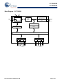
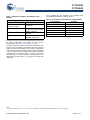
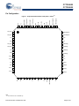
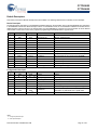
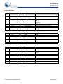
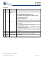
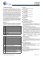
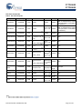
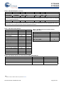
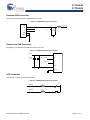
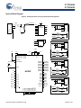
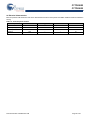
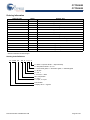
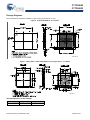
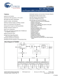
CY7C65620 CY7C65630 EZ-USB HX2LP™ Low Power USB 2.0 Hub Controller Family EZ-USB HX2LP™ Low Power USB 2.0 Hub Controller Family Features ■ Integrated upstream and downstream termination resistors ■ Integrated port status indicator control ■ 24 MHz external crystal (integrated phase-locked loop (PLL)) In-system EEPROM programming ■ USB 2.0 hub controller ■ Automotive and Industrial grade option (–40 °C to 85 °C) ■ Compliant with USB 2.0 specification ■ ■ USB-IF certified: TID# 30000009 ■ ■ Windows Hardware Quality Lab (WHQL) Compliant ■ Up to four downstream ports supported ■ Supports bus powered and self powered modes ■ Single transaction translator (TT) ■ Bus power configurations ■ Fit, form, and function compatible with CY7C65640 and CY7C65640A (TetraHub™) ■ Space saving 56-pin QFN ■ Single power supply requirement ❐ Internal regulator for reduced cost ■ Integrated upstream pull-up resistor ■ Integrated pull-down resistors for all downstream ports Block Diagram – CY7C65630 D+ Configurable with external SPI EEPROM: ❐ Vendor ID, Product ID, Device ID (VID/PID/DID) ❐ Number of active ports ❐ Number of removable ports ❐ Maximum power setting for high-speed and full-speed ❐ Hub controller power setting ❐ Power-on timer ❐ Overcurrent detection mode ❐ Enabled and disabled overcurrent timer ❐ Overcurrent pin polarity ❐ Indicator pin polarity ❐ Compound device ❐ Enable full-speed only ❐ Disable port indicators ❐ Ganged power switching ❐ Self and bus powered compatibility ❐ Fully configurable string descriptors for multiple language support For a complete list of related documentation, click here. D- USB 2.0 PHY 24 MHz Crystal High-Speed USB Control Logic Serial Interface Engine PLL SPI_SCK SPI_SD SPI_CS SPI Communication Block USB Upstream Port Transaction Translator Hub Repeater TT RAM Routing Logic USB Downstream Port 1 USB 2.0 PHY D+ D- Port Status Port Power Control USB Downstream Port 2 USB 2.0 PHY PWR#[1] LED D+ OVR#[1] Port Power Control D- PWR#[2] Port Status OVR#[2] LED USB Downstream Port 4 USB Downstream Port 3 Port Power Control USB 2.0 PHY D+ D- Port Status USB 2.0 PHY PWR#[3] LED D+ OVR#[3] D- Port Power Control Port Status PWR#[4] LED OVR#[4] Errata: For information on silicon errata, see “Errata” on page 28. Details include trigger conditions, devices affected, and proposed workaround. Cypress Semiconductor Corporation Document Number: 38-08037 Rev. AB • 198 Champion Court • San Jose, CA 95134-1709 • 408-943-2600 Revised January 7, 2015 CY7C65620 CY7C65630 Block Diagram – CY7C65620 D+ D- USB 2.0 PHY 24 MHz Crystal High-Speed USB Control Logic Serial Interface Engine PLL SPI Communication Block USB Upstream Port SPI_SCK SPI_SD SPI_CS Transaction Translator (X1) Hub Repeater TT RAM Routing Logic USB Downstream Port 1 USB 2.0 PHY D+ Port Power Control D- PWR#[1] Document Number: 38-08037 Rev. AB Port Status OVR#[1] LED USB Downstream Port 2 USB 2.0 PHY D+ D- Port Power Control Port Status PWR#[2] LED OVR#[2] Page 2 of 32 CY7C65620 CY7C65630 More Information Cypress provides a wealth of data at www.cypress.com to help you to select the right <product> device for your design, and to help you to quickly and effectively integrate the device into your design. For a comprehensive list of resources, see the knowledge base article http://www.cypress.com/?id=2411. ■ ■ ■ Overview: USB Portfolio, USB Roadmap USB 2.0 Product Selectors: HX2LP, HX2VL Application notes: Cypress offers a large number of USB application notes covering a broad range of topics, from basic to advanced level. Recommended application notes for getting started with FX2LP are: ❐ AN49150 - Schematic and Layout Review Checklist for HX2LP ❐ AN5044 - EZ-USB Hubs(CY7C656XX) PCB Design Recommendations ❐ AN15454 - Bus-Powered USB Hub Design Using EZ-USB HX2LP™/HX2VL AN61904 - How HX2LP™ Addresses Byte and Word-Addressable SPI EEPROMs ❐ AN69235 - Migrating from HX2/HX2LP to HX2VL ❐ AN5038 - Migrating From EZ-USB® HX2™ to EZ-USB HX2LP™ ❐ ■ Reference Designs: ❐ CY4605 - High-Speed Low-Power USB 2.0 Compliant 2-Port Hub ❐ CY4606 - EZ-USB HX2LP High-Speed Low-Power USB 2.0 Compliant 4-Port Hub ■ Models: HX2LP EZ-USB® HX2LPTM Reference Design Kit (RDK) EZ-USB® HX2LP™ Reference Design Kit (RDK) board is a tool to demonstrate the features of EZ-USB HX2LP devices (CY7C65620/CY7C65630). Both CY7C65620 and CY7C65630 are identical in every aspect except for the number of ports they support. The HX2LP RDK is based on the 56-pin QFN for CY7C65620/CY7C65630. Both are single transaction translator (1TT) hubs. In the initial phase of the design, this board helps developers to understand the chip features and limitations before proceeding with a complete design. The RDK includes support documents related to board hardware, PC application software, and EEPROM configuration data (.iic) files. Document Number: 38-08037 Rev. AB Page 3 of 32 CY7C65620 CY7C65630 Contents Introduction ....................................................................... 5 USB Serial Interface Engine ........................................ 5 Hub Repeater .............................................................. 5 Transaction Translator ................................................ 5 Applications ...................................................................... 5 Functional Overview ........................................................ 5 System Initialization ..................................................... 5 Enumeration ................................................................ 5 Downstream Ports ....................................................... 6 Upstream Port ............................................................. 6 Power Switching .......................................................... 6 Overcurrent Detection ................................................. 6 Port Indicators ............................................................. 6 Pin Configuration ............................................................. 8 Pin Definitions .................................................................. 9 Default Descriptors ........................................................ 11 Device Descriptor ...................................................... 11 Configuration Descriptor ............................................ 11 Interface Descriptor ................................................... 12 Endpoint Descriptor ................................................... 12 Device Qualifier Descriptor ........................................ 12 Hub Descriptor .......................................................... 13 Configuration Options ................................................... 14 0xD0 Load ................................................................. 14 0xD2 Load ................................................................. 14 0xD4 Load ................................................................. 15 Supported USB Requests .............................................. 18 Device Class Commands .......................................... 18 Hub Class Commands .............................................. 19 Document Number: 38-08037 Rev. AB Upstream USB Connection ............................................ 21 Downstream USB Connection ....................................... 21 LED Connection .............................................................. 21 System Block Diagram ................................................... 22 Absolute Maximum Ratings .......................................... 23 Operating Conditions ..................................................... 23 Electrical Characteristics ............................................... 23 DC Electrical Characteristics ..................................... 23 USB Transceiver ....................................................... 23 AC Electrical Characteristics ..................................... 24 Ordering Information ...................................................... 25 Ordering Code Definitions ......................................... 25 Package Diagrams .......................................................... 26 Thermal Impedance for the Package ........................ 26 Acronyms ........................................................................ 27 Document Conventions ................................................. 27 Units of Measure ....................................................... 27 Numeric Naming ........................................................ 27 Errata ............................................................................... 28 Part Numbers Affected .............................................. 28 HX2LP Qualification Status ....................................... 28 HX2LP Errata Summary ............................................ 28 Document History Page ................................................. 29 Sales, Solutions, and Legal Information ...................... 32 Worldwide Sales and Design Support ....................... 32 Products .................................................................... 32 PSoC® Solutions ....................................................... 32 Cypress Developer Community ................................. 32 Technical Support ..................................................... 32 Page 4 of 32 CY7C65620 CY7C65630 Introduction EZ-USB HX2LP™ is Cypress’s next generation family of high-performance, low-power USB 2.0 hub controllers. HX2LP is an ultra low power single chip USB 2.0 hub controller with integrated upstream and downstream transceivers, a USB serial interface engine (SIE), USB hub control and repeater logic, and TT logic. Cypress has also integrated many of the external passive components, such as pull-up and pull-down resistors, reducing the overall bill of materials required to implement a hub design. The HX2LP portfolio consists of: ■ CY7C65630: 4-port/single transaction translator This device option is for ultra low-power applications that require four downstream ports. All four ports share a single transaction translator. The CY7C65630 is available in 56 QFN and is also pin-for-pin compatible with the CY7C65640. ■ CY7C65620: 2-port/single transaction translator This device option is for a 2-port bus powered application. Both ports share a single transaction translator. The CY7C65620 is available in a 56 QFN. All device options are supported by Cypress’s world class reference design kits, which include board schematics, bill of materials, Gerber files, Orcad files, and thorough design documentation. USB Serial Interface Engine The serial interface engine (SIE) allows the CY7C65620/CY7C65630 to communicate with the USB host. The SIE handles the following USB activities independently of the Hub Control Block. the route only includes the repeater and no TT, because the device and the hub are operating at the same speed. When the hub is operating at full-speed (the upstream port is connected to a full-speed host controller), a high-speed peripheral does not operate at its full capability. These devices only work at full-speed. Full- and low-speed devices connected to this hub operate at their normal speed. Applications Typical applications for the HX2LP device family are: ■ Standalone hubs ■ Motherboard hubs ■ Monitor hubs ■ Advanced port replicators ■ Docking stations ■ Split-PC designs ■ External personal storage drives ■ Keyboard hubs Functional Overview The Cypress CY7C65620/CY7C65630 USB 2.0 Hubs are high-performance, low system cost solutions for USB. The CY7C65620/CY7C65630 USB 2.0 Hubs integrate 1.5 k upstream pull-up resistors for full-speed operation and all downstream 15 k pull-down resistors and series termination resistors on all upstream and downstream D+ and D– pins. This results in optimization of system costs by providing built-in support for the USB 2.0 specification. ■ Bit stuffing and unstuffing ■ Checksum generation and checking System Initialization ■ TOKEN type identification ■ Address checking. On power-up, the CY7C65620/CY7C65630 reads an external SPI EEPROM for configuration information. At the most basic level, this EEPROM has the vendor ID (VID), product ID (PID), and device ID (DID) for the customer’s application. For more specialized applications, other configuration options can be specified. See Configuration Options on page 14 for more details. Hub Repeater The hub repeater manages the connectivity between upstream and downstream facing ports that are operating at the same speed. It supports full- or low-speed connectivity and high-speed connectivity. According to the USB 2.0 specification, the HUB Repeater provides the following functions: ■ Sets up and tears down connectivity on packet boundaries ■ Ensures orderly entry into and out of the suspend state, including proper handling of remote wakeups. Transaction Translator The TT translates data from one speed to another. A TT takes high speed split transactions and translates them to full- or low-speed transactions when the hub is operating at high-speed (the upstream port is connected to a high-speed host controller) and has full- or low-speed devices attached. The operating speed of a device attached on a downstream facing port determines whether the routing logic connects a port to the TT or hub repeater. If a full- or low-speed device is connected to the hub operating at high-speed, the data transfer route includes the TT. If a high-speed device is connected to this high-speed hub, Document Number: 38-08037 Rev. AB After reading the EEPROM, if VBUSPOWER (connected to upstream VBUS) is high, CY7C65620/CY7C65630 enables the pull-up resistor on D+ to indicate its presence to the upstream hub, after which a USB bus reset is expected. During this reset, CY7C65620/CY7C65630 initiates a chirp to indicate that it is a high-speed peripheral. In a USB 2.0 system, the upstream hub responds with a chirp sequence, and CY7C65620/CY7C65630 is in a high-speed mode, with the upstream D+ pull-up resistor turned off. In USB 1.x systems, no such chirp sequence from the upstream hub is seen, and CY7C65620/CY7C65630 operates as a normal 1.x hub (operating at full-speed). Enumeration After a USB bus reset, CY7C65620/CY7C65630 is in an unaddressed, unconfigured state (configuration value set to ’0’). During the enumeration process, the host sets the hub's address and configuration. After the hub is configured, the full hub functionality is available. Page 5 of 32 CY7C65620 CY7C65630 Downstream Ports The CY7C65620/CY7C65630 supports a maximum of four downstream ports, each of which may be marked as usable or removable in the extended configuration (0xD2 EEPROM load or 0xD4 EEPROM load, see Configuration Options on page 14. Downstream D+ and D– pull-down resistors are incorporated in CY7C65620/CY7C65630 for each port. Before the hubs are configured, the ports are driven SE0 (single ended zero, where both D+ and D– are driven low) and are set to the unpowered state. When the hub is configured, the ports are not driven and the host may power the ports by sending a SetPortPower command for each port. After a port is powered, any connect or disconnect event is detected by the hub. Any change in the port state is reported by the hubs back to the host through the status change endpoint (endpoint 1). On receipt of SetPortReset request for a port with a device connected, the hub does as follows: ■ Performs a USB reset on the corresponding port ■ Puts the port in an enabled state ■ Enables the green port indicator for that port (if not previously overridden by the host) ■ Enables babble detection after the port is enabled. Babble consists of a non-idle condition on the port after EOF2. If babble is detected on an enabled port, that port is disabled. A ClearPortEnable request from the host also disables the specified port. Downstream ports can be individually suspended by the host with the SetPortSuspend request. If the hub is not suspended, a remote wakeup event on that port is reflected to the host through a port change indication in the hub status change endpoint. If the hub is suspended, a remote wakeup event on this port is forwarded to the host. The host may resume the port by sending a ClearPortSuspend command. Upstream Port The upstream port includes the transmitter and the receiver state machine. The transmitter and receiver operate in high-speed and full-speed depending on the current hub configuration. The transmitter state machine monitors the upstream facing port while the hub repeater has connectivity in the upstream direction. This machine prevents babble and disconnect events on the downstream facing ports of this hub from propagating and causing the hub to be disabled or disconnected by the hub to which it is attached. Power Switching The CY7C65620/CY7C65630 includes interface signals for external port power switches. Both ganged and individual (per-port) configurations are supported, with individual switching being the default. Initially all ports are unpowered. After enumerating, the host may power each port by sending a SetPortPower request for that port. The power switching and overcurrent detection of downstream ports is managed by control pins connected to an external power switch device. PWR Document Number: 38-08037 Rev. AB [n]# output pins of the CY7C65620/CY7C65630 series are connected to the respective external power switch's port power enable signals. Note that each port power output pin of the external power switch must be bypassed with an electrolytic or tantalum capacitor as required by the USB specification. These capacitors supply the inrush currents, which occur during downstream device hot-attach events. The polarity of this pin is configured through the EEPROM; see Configuration Options on page 14. Overcurrent Detection Overcurrent detection includes 8 ms of timed filtering by default. This parameter is configured from the external EEPROM in a range of 0 ms to 15 ms for both enabled ports and disabled ports individually. Detection of overcurrent on downstream ports is managed by control pins connected to an external power switch device. The OVR[n]# pins of the CY7C65620/CY7C65630 series are connected to the respective external power switch’s port overcurrent indication (output) signals. After detecting an overcurrent condition, hub reports overcurrent condition to the host and disables the PWR# output to the external power device. The polarity of the OVR pins can be configured through the EEPROM; see Configuration Options on page 14. Port Indicators The USB 2.0 port indicators are also supported directly by CY7C65620/CY7C65630. According to the specification, each downstream port of the hub optionally supports a status indicator. The presence of indicators for downstream facing ports is specified by bit 7 of the wHubCharacteristics field of the hub class descriptor. The default CY7C65620/CY7C65630 descriptor specifies that port indicators are supported (wHubCharacteristics, bit 7 is set). If port indicators are not included in the hub, disable this bit through EEPROM settings. Each port indicator pin is strategically located directly on the opposite edge of the port with which it is associated. A port indicator provides two colors: green and amber. This is usually implemented as two separate LEDs, one amber and the other green. A combination of hardware and software control is used to inform the user of the current status of the port or the device attached to the port and to guide the user through problem resolution. Colors and blinking provide information to the user. The significance of the color of the LED depends on the operational mode of CY7C65620/CY7C65630. The CY7C65620/CY7C65630 port indicators has two modes of operation: automatic and manual. On power up the CY7C65620/CY7C65630 defaults to automatic mode, where the color of the Port Indicator (green, amber, off) indicates the functional status of the CY7C65620/CY7C65630 port. In automatic mode, the CY7C65620/CY7C65630 turns on the green LED whenever the port is enabled and the amber LED when an overcurrent condition is detected. The color of the port indicator is set by the port state machine. Blinking of the LEDs is not supported in automatic mode. Table 1 identifies the mapping of color to port state in automatic mode. Page 6 of 32 CY7C65620 CY7C65630 Table 1. Automatic Port State to Port Indicator Color Mapping Downstream Facing Hub Port State Color Definition Port State Table 2 displays the color definition of the indicators when CY7C65620/CY7C65630 is in manual mode.[1] Table 2. Port Indicator Color Definitions in Manual Mode Color Definition Port State Off Not operational Amber Error condition Off or Amber, if due to an overcurrent condition Powered Off Off Disconnected, Disabled, Not Configured, Resetting, Testing Green Fully operational Software attention Green Enabled, Transmit, or TransmitR Blinking Off / Green Blinking Off / Amber Hardware attention Blinking Green / Amber Reserved Off Suspended, Resuming, SendEOR, Restart_E/S The LED control lines can also be modulated with a square wave for power conservation. The polarity of these pins is programmable, see Configuration Options on page 14. In manual mode, the indicators are under the control of the host, which can turn on the LEDs, or leave them off. This is done by a USB Hub class request. Blinking of the LEDs is supported in manual mode. The port indicators enable the user to intervene in any error detection. For example, when babble is detected while plugging in a defective device, or when an overcurrent condition occurs, the port indicators corresponding to the downstream port blink green or only light the amber LED, respectively. Note 1. Information presented in <ref_note>Table 1 and <ref_note>Table 2 is from USB 2.0 specification Tables 11-6 and 11-7, respectively. Document Number: 38-08037 Rev. AB Page 7 of 32 CY7C65620 CY7C65630 Pin Configuration DD–[4]/NC DD+[4]/NC VCC 54 51 50 49 48 47 46 45 44 GREEN#[4]/NC AMBER#[4]/NC SELFPWR RESET GND SPI_SCK SPI_SD 52 GND 53 OVR#[4]/Rsvd PWR#[4]/NC PWR#[3]/NC 55 OVR#[3]/Rsvd 56 VCC GND Figure 1. 56-pin Quad Flat Pack No Leads (8 mm × 8 mm) [2] 43 1 42 AMBER#[3]/NC 2 41 GREEN#[3]/NC 3 40 GND 4 GND 39 VCC DD–[3]/NC 5 38 AMBER#[2] DD+[3]/NC 6 37 GREEN#[2] VCC 7 36 AMBER#[1] GND 8 35 GREEN#[1] DD–[2] 9 34 GND DD+[2] 10 33 VCC VCC 11 32 OVR#[2] GND 12 31 PWR#[2] DD–[1] 13 30 OVR#[1] DD+[1] 14 21 22 23 24 25 GND XIN XOUT VCC GND SPI_CS 26 27 28 GND 20 VCC 19 VBUSPOWER 18 VCC 17 D– 16 GND VCC 15 D+ 29 PWR#[1] Note 2. NC and Rsvd are for CY7C65620 only. Document Number: 38-08037 Rev. AB Page 8 of 32 CY7C65620 CY7C65630 Pin Definitions Table 3. Pin Assignments [3] Pin CY7C65630 Name CY7C65620 Name 3 7 11 15 19 23 27 33 39 55 VCC VCC VCC VCC VCC VCC VCC VCC VCC VCC VCC VCC VCC VCC VCC VCC VCC VCC VCC Power Power Power Power Power Power Power Power Power N/A N/A N/A N/A N/A N/A N/A N/A N/A VCC. This signal provides power to the chip. VCC. This signal provides power to the chip. VCC. This signal provides power to the chip. VCC. This signal provides power to the chip. VCC. This signal provides power to the chip. VCC. This signal provides power to the chip. VCC. This signal provides power to the chip. VCC. This signal provides power to the chip. VCC. This signal provides power to the chip. 4 8 12 16 20 24 28 34 40 47 50 56 21 22 GND GND GND GND GND GND GND GND GND GND GND GND XIN XOUT VCC GND GND GND GND GND GND GND GND GND GND GND GND XIN XOUT Power Power Power Power Power Power Power Power Power Power Power Power Power Input Output N/A N/A N/A N/A N/A N/A N/A N/A N/A N/A N/A N/A N/A N/A N/A 46 RESET# RESET# Input N/A 45 SELFPWR SELFPWR Input N/A VBUSPOWER VBUSPOWER Input N/A VCC. This signal provides power to the chip. GND. Connect to ground with as short a path as possible. GND. Connect to ground with as short a path as possible. GND. Connect to ground with as short a path as possible. GND. Connect to ground with as short a path as possible. GND. Connect to ground with as short a path as possible. GND. Connect to ground with as short a path as possible. GND. Connect to ground with as short a path as possible. GND. Connect to ground with as short a path as possible. GND. Connect to ground with as short a path as possible. GND. Connect to ground with as short a path as possible. GND. Connect to ground with as short a path as possible. GND. Connect to ground with as short a path as possible. 24 MHz crystal IN or external clock input. 24 MHz crystal OUT. (NC if external clock is used) Active LOW reset. This pin resets the entire chip. It is normally tied to VCC through a 100 K resistor, and to GND through a 0.1 µF capacitor. No other special power-up procedure is required. Self power. Indicator for bus or self powered. 0 is bus powered, 1 is self powered. VBUS. Connect to the VBUS pin of the upstream connector. This signal indicates to the hub that it is in a connected state, and may enable the D+ pull-up resistor to indicate a connection. (The hub does so after the external EEPROM is read). 26 SPI Interface 25 SPI_CS 48 SPI_SCK 49 SPI_SD Upstream Port 17 D– 18 D+ Type Default SPI_CS SPI_SCK Output Output O O SPI_SD I/O/Z Z D– D+ I/O/Z I/O/Z Z Z Description SPI chip select. Connect to CS pin of the EEPROM. SPI clock. Connect to EEPROM SCK pin. SPI dataline connect to GND with 15 kresistor and to the Data I/O pin of the EEPROM. Upstream D– Signal. Upstream D+ Signal. Note 3. Unused port DD+/DD– lines can be left floating. Leave the port power, amber, and green LED pins unconnected, and deassert the overcurrent pin. Do not leave the overcurrent pin floating; it is an input. SPI data line should be connected to GND with 15 k resistor (Even if no EEPROM is used). Document Number: 38-08037 Rev. AB Page 9 of 32 CY7C65620 CY7C65630 Table 3. Pin Assignments [3] (continued) CY7C65630 Name Downstream Port 1 Pin CY7C65620 Name Type Default 13 14 DD–[1] DD+[1] DD–[1] DD+[1] I/O/Z I/O/Z Z Z 36 AMBER#[1] AMBER#[1] Output 1 35 GREEN#[1] GREEN#[1] Output 1 30 OVR#[1] OVR#[1] Input 1 29 PWR#[1] PWR#[1] O/Z Z DD–[2] DD+[2] I/O/Z I/O/Z Z Z Downstream Port 2 9 DD–[2] 10 DD+[2] 38 AMBER#[2] AMBER#[2] Output 1 37 GREEN#[2] GREEN#[2] Output 1 32 OVR#[2] OVR#[2] Input 1 31 PWR#[2] PWR#[2] O/Z Z NC NC I/O/Z I/O/Z Z Z Downstream Port 3 5 DD–[3] 6 DD+[3] 42 AMBER#[3] NC Output 1 41 GREEN#[3] NC Output 1 53 OVR#[3] Reserved Input 1 54 PWR#[3] NC O/Z Z Downstream Port 4 1 DD–[4] 2 DD+[4] NC NC I/O/Z I/O/Z Z Z 44 AMBER#[4] NC Output 1 43 GREEN#[4] NC Output 1 51 OVR#[4] Reserved Input 1 52 PWR#[4] NC O/Z Z Document Number: 38-08037 Rev. AB Description Downstream D– Signal. Downstream D+ Signal. LED. Driver output for Amber LED. Port indicator support. Default is active LOW. Polarity is controlled through EEPROM. LED. Driver output for Green LED. Port indicator support. Default is active LOW. Polarity is controlled through EEPROM. Overcurrent condition detection input. Default is active LOW. Polarity is controlled through EEPROM. Power switch driver output. Default is active LOW. Polarity is controlled through EEPROM. Downstream D– Signal. Downstream D+ Signal. LED. Driver output for amber LED. Port indicator support. Default is active LOW. Polarity is controlled through EEPROM. LED. Driver output for green LED. Port indicator support. Default is active LOW. Polarity is controlled through EEPROM. Overcurrent condition detection input. Default is active LOW. Polarity is controlled through EEPROM. Power switch driver output. Default is active LOW. Polarity is controlled through EEPROM. Downstream D– Signal. Downstream D+ Signal. LED. Driver output for amber LED. Port indicator support. Default is active LOW. Polarity is controlled through EEPROM. LED. Driver output for Green LED. Port indicator support. Default is active LOW. Polarity is controlled through EEPROM. Overcurrent condition detection input. Default is active LOW. Polarity is controlled through EEPROM. Reserved. Pull to deasserted state with external resistor (CY7C65620 only) Power switch driver output. Default is active LOW. Polarity is controlled through EEPROM. Downstream D– Signal. Downstream D+ Signal. LED. Driver output for amber LED. Port indicator support. Default is active LOW. Polarity is controlled through EEPROM. LED. Driver output for green LED. Port indicator support. Default is active LOW. Polarity is controlled through EEPROM. Overcurrent condition detection input. Default is active LOW. Polarity is controlled through EEPROM. Reserved. Pull to deasserted state with external resistor (CY7C65620 only) Power switch driver output. Default is active LOW. Polarity is controlled through EEPROM. Page 10 of 32 CY7C65620 CY7C65630 Default Descriptors This section presents the different descriptors that are available. The following tables list the functionality of each descriptor. Device Descriptor The standard device descriptor for CY7C65620/CY7C65630 is based on the information found in the SPI EEPROM. The information in the EEPROM overrides the default descriptor values. If no EEPROM is used, the CY7C65620/CY7C65630 enumerates with the default descriptor values as shown in the following table. If a blank EEPROM is connected, the hub enumerates as vendor defined class instead of a hub class. This is for the purpose of programming the EEPROM with the Cypress driver. Byte Full Speed High Speed 0 0x12 0x12 1 0x01 0x01 2,3 0x0110 0x0200 4 0x09 5 0x00 6 7 Field Name bLength Description 18 bytes bDescriptorType DEVICE_DESCRIPTOR bcdUSB USB specification 2.0 (1.1 if forced FS) 0x09 bDeviceClass HUB 0x00 bDeviceSubClass None 0x00 0x01 bDeviceProtocol None 0x40 0x40 bMaxPacketSize0 64 bytes 8,9 0x04B4 0x04B4 wIdVendor VID (overridden by what is defined in EEPROM) 10,11 0x6560 0x6560 wIdProduct PID (overridden by what is defined in EEPROM) 12, 13 0x0915 0x0915 14 0x00 0x00 wbcdDevice DID (overridden by what is defined in EEPROM) iManufacturer Overridden by EEPROM 15 0x00 0x00 iProduct Overridden by EEPROM 16 0x00 0x00 iSerialNumber Overridden by EEPROM 17 0x01 0x01 bNumConfigurations One configuration supported Configuration Descriptor Byte Full Speed High Speed 0x09 Field Name bLength Description 0 0x09 1 0x02[4]/0x07[5] 2 0x0019 0x0019 wTotalLength Length of all other descriptors 4 0x01 0x01 bNumInterfaces 1 5 0x01 0x01 bConfigurationValue The configuration to use 6 0x00 0x00 iConfiguration Index of string descriptor describing this configuration 7 0xA0 0xE0 0xA0 0xE0 bmAttributes Value depends on pin 45 - SELFPWR signal SELFPWR = 0 yields 0xA0 and =1 yields 0xE0 8 0x28 0x57[4] bMaxPower Maximum power consumption of hub from the USB bus 0x02[4]/0x07[5] bDescriptorType 9 bytes CONFIG_DESCRIPTOR Notes 4. Configured speed descriptor. 5. Other speed descriptor. Document Number: 38-08037 Rev. AB Page 11 of 32 CY7C65620 CY7C65630 Interface Descriptor Byte Full Speed High Speed 0 0x09 0x09 1 0x04 2 0x00 3 0x00 4 Field Name Description bLength 9 bytes 0x04 bDescriptorType INTERFACE_DESCRIPTOR 0x00 bInterfaceNumber Number of this interface 0x00 bAlternateSetting Value used to select this alternate setting for the interface 0x01 0x01 bNumEndpoints Number of endpoints used by this interface (not including endpoint 0) 5 0x09 0x09 bInterfaceClass Hub class code 6 0x00 0x00 bInterfaceSubClass Subclass code (assigned by the USB-IF) 7 0x00 0x00 bInterfaceProtocol Protocol code (assigned by the USB-IF) 8 0x00 0x00 iInterface Index of the string descriptor describing this interface Endpoint Descriptor Byte Full-Speed High-Speed Field Name Description 0 0x07 0x07 bLength 7 bytes 1 0x05 0x05 bDescriptorType ENDPOINT_DESCRIPTOR 2 0x81 0x81 bEndpointAddress IN Endpoint #1 3 0x03 0x03 bmAttributes Interrupt 4, 5 0x0001 0x0001 6 0xFF 0x0C wMaxPacketSize Maximum packet size bInterval Polling rate Device Qualifier Descriptor Byte Full-Speed High-Speed 0 0x0A 0x0A bLength 10 bytes 1 0x06 0x06 bDescriptorType DEVICE_QUALIFIER 2, 3 0x0200 0x0200 bcdUSB USB Specification Release Number in Binary-Coded Decimal 4 0x09 0x09 bDeviceClass Class code (assigned by the USB-IF) 5 0x00 0x00 bDeviceSubClass Subclass code (assigned by the USB-IF) 6 0x01 0x00 bDeviceProtocol Protocol code (assigned by the USB-IF) 7 0x40 0x40 bMaxPacketSize0 Maximum packet size for other speed 8 0x01 0x01 bNumConfigurations Number of other-speed configurations 9 0x00 0x00 bReserved Reserved for future use, must be zero Document Number: 38-08037 Rev. AB Field Name Description Page 12 of 32 CY7C65620 CY7C65630 Hub Descriptor Byte All Speed Field Name Description 0 0x09 bLength 9 bytes 1 0x29 bDescriptorType HUB descriptor 2 0x04[6] 0x02 bNbrPorts Number of ports supported, CY7C65630 Number of ports supported, CY7C65620 wHubCharacteristics b1, b0: Logical power switching mode 00: Ganged power switching (all ports’ power at once). 01: Individual port power switching (Default in CY7C65620/CY7C65630). b2: Identifies a compound device 0: Hub is not part of a compound device (Default in CY7C65620/CY7C65630). 1: Hub is part of a compound device. b4, b3: Overcurrent protection mode 00: Global overcurrent protection. The hub reports overcurrent as a summation of all ports’ current draw, without a breakdown of individual port overcurrent status. 01: Individual port overcurrent protection. The hub reports overcurrent on a per-port basis. Each port has an overcurrent status (Default in CY7C65620/CY7C65630). 1X: No overcurrent protection. This option is allowed only for bus powered hubs that do not implement overcurrent protection. b6, b5: TT think time 00: TT requires at most eight FS bit times of inter transaction gap on a full/lowspeed downstream bus (Default in CY7C65620/CY7C65630). b7: Port indicators supported, 0: Port indicators are not supported on its downstream facing ports and the SetPortIndicator request has no effect. 1: Port indicators are supported on its downstream facing ports and the SetPortIndicator request controls the indicators. See “Functional Overview” on page 5 and “Supported USB Requests” on page 18. (Default in CY7C65620/CY7C65630). b15, b8: Reserved 3,4 0x0089[6] 5 0x32[6] bPwrOn2PwrGood Time from when the port is powered to when the power is good on that port. 6 0x28[6] 0xAE[6] bHubContrCurrent Maximum current requirement for the hub controller at full-speed. Maximum current requirement for the hub controller at high-speed. 7 0x00[6] bDeviceRemovable Indicates if the logical port has a removable device attached (0 = removable, 1 = non removable). 8 0xFF[6] bPortPwrCtrlMask Required for compatibility with software written for 1.0 compliant devices. Note 6. This value is configured through the external EEPROM. Document Number: 38-08037 Rev. AB Page 13 of 32 CY7C65620 CY7C65630 Configuration Options Byte 0: 0xD2 Systems using CY7C65620/CY7C65630 have the option of using a fuse ROM, which is preset at the factory to configure the hub. Otherwise, it must have an external EEPROM for the device to have a unique VID, PID, and DID. The CY7C65620/CY7C65630 can communicate with SPI EEPROM that are either double byte addressed or single byte with the ninth bit within the instruction byte, such as the 24LC040 parts use. The 25LC080 EEPROM uses the double byte address format. Therefore, the CY7C65620/CY7C65630 can communicate with these parts. The '010s and '020s use the same command format that is used to interface with the ‘040 and hence these can also be used to interface with the CY7C65620/CY7C65630. If the attached EEPROM is blank (0xFF) the hub enumerates as a vendor class device. In this configuration, the hub connects to the Cypress driver to allow programming of the EEPROM. When the EEPROM is programmed, a power cycle configures the chip as a hub class device. With this EEPROM format, only a unique VID, PID, and DID must be present in the external SPI EEPROM. The contents of the EEPROM must contain this information in the following format: Byte Value 0xD0 1 VID (LSB) 2 VID (MSB) 3 PID (LSB) 4 PID (MSB) 5 reserved 6 DID (MSB) Most significant byte of vendor ID Byte 3: PID (LSB) Least significant byte of product ID Byte 4: PID (MSB)] Most significant byte of product ID Byte 5: Reserved Reserved Byte 6: DID (MSB)] Most significant byte of device ID Count time in ms for filtering overcurrent detection. Bits 7–4 are for an enabled port, and bits 3–0 are for a disabled port. Both range from 0 ms to 15 ms. See Port Indicators on page 6. Default: 8 ms = 0x88. Byte 8: ActivePorts[3:0], RemovablePorts[3:0] Bits 7–4 are the ActivePorts[3:0] bits that indicates if the corresponding port is usable. For example, a two-port hub that uses ports 1 and 4 would set this field to 0x09. The total number of ports reported in the Hub Descriptor: bNbrPorts field is calculated from this. Bits 3–0 are the RemovablePorts[3:0] bits that indicates whether the corresponding logical port is removable (set to high). Logical port numbers are from 1 to n where n is the total number of active ports. If port 2 is disabled then physical ports 1, 3, and 4 map to logical ports 1, 2, and 3. These bit values are reported appropriately in the HubDescriptor:DeviceRemovable field. Default: 0xFF. 0xD2 Load Byte Least significant byte of vendor ID Byte 2: VID (MSB) Byte 7: EnabledOvercurrentTimer[3:0], DisabledOvercurrentTimer[3:0] 0xD0 Load 0 Needs to be programmed with 0xD2 Byte 1: VID (LSB) Value (MSBLSB) 0 0xD2 1 VID (LSB) 2 VID (MSB) 3 PID (LSB) 4 PID (MSB) 5 reserved 6 DID (MSB) 7 EnabledOverCurrentTimer[3:0], DisableOvercurrentTimer[3:0] 8 ActivePorts[3:0], RemovablePorts[3:0] 9 MaxPower 10 HubControllerPower 11 PowerOnTimer 12 IllegalHubDescriptor, CompoundDevice, FullspeedOnly, NoPortIndicators, Reserved, GangPowered, Reserved, Reserved Document Number: 38-08037 Rev. AB Byte 9: MaximumPower This value is reported in the ConfigurationDescriptor:bMaxPower field and is the current in 2 mA increments that is required from the upstream hub. Default: 0x28 = 80 mA for full-speed and 0x57 = 174 mA for high-speed. Byte 10: HubControllerPower This value is reported in the HubDescriptor:bHubContrCurrent field and is the current in milliamperes required by the hub controller. Default: 0x50 = 80 mA for full-speed and 0xAE = 174 mA for high-speed. Byte 11: PowerOnTimer This value is reported in the HubDescriptor:bPwrOn2PwrGood field and is the time in 2 ms intervals from the SetPortPower command until the power on the corresponding downstream port is good. Default: 0x32 = 100 ms. Page 14 of 32 CY7C65620 CY7C65630 Byte 12: IllegalHubDescriptor, CompoundDevice, Full Speed Only, NoPortIndicators, Reserved, GangPowered, Reserved, Reserved Bit 7: IllegalHubDescriptor. For GetHubDescriptor request, some USB hosts use a DescriptorTypeof 0x00 instead of HUB_DESCRIPTOR, 0x29. According to the USB 2.0 standard, a hub must treat this as a Request Error, and STALL the transaction accordingly (USB 2.0, 11.24.2.5). For systems that do not accept this, the IllegalHubDescriptor configuration bit can be set to allow CY7C65620/CY7C65630 to accept a DescriptorType of 0x00 for this command. Default is 1. Bit 6: CompoundDevice. Indicates whether the hub is part of a compound device. This is reported in the HubDescriptor, wHub-Characteristics: b2. Default set to ‘0’. Bit 5: Fullspeed. Only configures the hub to be a full-speed only device. Default is set to ‘0’. Bit 4: NoPortIndicators. Turns off the port indicators and does not report them as present in the HubDescriptor, wHubCharacteristics b7 field. Default is set to ‘0’. Bit 3: Reserved. Set this bit to ‘0’. Bit 2: GangPowered. Indicates whether the port power switching is ganged (set to 1) or per-port (set to ‘0’). This is reported in the HubDescriptor, wHubCharacteristics field, b4, b3, b1, and b0. Default is set to ‘0’. Bit 1: Reserved. Default is set to ‘0’. Bit 0: Reserved. Default is set to ‘0’. 0xD4 Load Byte 0 1 2 3 4 5 6 7 8 9 10 11 12 13 14 Value (MSB LSB) 0xD4 VID (LSB) VID (MSB) PID (LSB) PID (MSB) reserved DID (MSB) EnabledOverCurrentTimer[3:0], DisableOvercurrentTimer[3:0] MaxPower (full-speed) MaxPower (high-speed) Reserved Reserved HubControllerPower full-speed bus powered HubControllerPower high-speed bus powered HubControllerPower full-speed self powered Document Number: 38-08037 Rev. AB Factory Fusable X X X X 0xD4 Load (continued) Byte Factory Fusable Value (MSB LSB) HubControllerPower high-speed self powered 16 PowerOnTimer IllegalHubDescriptor, CompoundDevice, FullspeedOnly, 17 NoPortIndicators, Reserved, GangPowered, Reserved, Reserved AmberPolarity, GreenPolarity, ModulateIndicators, PowerControlPolarity, 18 OverCurrentPolarity, OverCurrentMode1, OverCurrentMode2 19 Write protect 20 NumLangs 21 SupportedStrings 22 ActivePorts[3:0] 23 RemovablePorts[3:0] 24 LangID a=24+2N iManufacturer b=a+2N iProduct c=b+2N iSerialNumber d=c+2N iConfiguration(FS) e=d+2N iConfiguration(HS) f=e+2N iInterface(0) g=f+2N reserved h=g+2N Strings N:NumLangs 15 X X X Byte 0: 0xD4 Needs to be programmed with 0xD4 Byte 1: VID (LSB) X Least significant byte of vendor ID Byte 2: VID (MSB) X X Most significant byte of vendor ID Byte 3: PID (LSB) Least significant byte of product ID Byte 4: PID (MSB) X X Most significant byte of product ID Byte 5: Reserved Reserved Byte 6: DID (MSB) Most significant byte of device ID Page 15 of 32 CY7C65620 CY7C65630 Byte 7: EnabledOvercurrentTimer[3:0], DisabledOvercurrentTimer[3:0] Count time in ms for filtering overcurrent detection. Bits 7–4 are for an enabled port, and bits 3–0 are for a disabled port. Both range from 0 ms to 15 ms. See Port Indicators on page 6. Default: 8 ms = 0x88. Byte 8: MaximumPower (Full-speed) This value is reported in the ConfigurationDescriptor:bMaxPower field and is the current in 2 mA increments that is required from the upstream hub when connected at full-speed. Default: 0x28 = 80 mA for full-speed. Byte 9: MaximumPower (High-speed) This value is reported in the ConfigurationDescriptor:bMaxPower field and is the current in 2 mA increments that is required from the upstream hub when connected at high-speed. Default: 0x57 = 174 mA for high-speed. Byte 10: Reserved Write zeros to this location. Byte 11: Reserved Write zeros to this location. Byte 12: HubControllerPower (Full-speed, bus-powered) This value is reported in the HubDescriptor:bHubContrCurrent field and is the current in milliamperes required by the hub controller when connected on the upstream hub as a full-speed. Default: 0x50 = 80 mA for full-speed. Byte 13: HubControllerPower (High-speed, bus-powered) This value is reported in the HubDescriptor:bHubContrCurrent field and is the current in milliamperes required by the hub controller when connected on the upstream hub as a high-speed. Default: 0xAE = 174 mA for high-speed. Byte 14: HubControllerPower (Full-speed, self-powered) This value is reported in the HubDescriptor:bHubContrCurrent field and is the current in milliamperes required by the hub controller when connected on the upstream hub as a full-speed. Default: 0x50 = 80 mA for full-speed. Byte 15: HubControllerPower (High-speed, self-powered) This value is reported in the HubDescriptor:bHubContrCurrent field and is the current in milliamperes required by the hub controller when connected on the upstream hub as a high-speed. Default: 0x64 = 100 mA for high-speed. Byte 16: PowerOnTimer This value is reported in the HubDescriptor:bPwrOn2PwrGood field and is the time in 2 ms increments from the SetPortPower command until the power on the corresponding downstream port is good. Default: 0x32 = 100 ms. Document Number: 38-08037 Rev. AB Byte 17: IllegalHubDescriptor, CompoundDevice, Full-Speed Only, NoPortIndicators, Reserved, GangPowered, Reserved, Reserved Bit 7: IllegalHubDescriptor. For GetHubDescriptor request, some USB hosts use a DescriptorTypeof 0x00 instead of HUB_DESCRIPTOR, 0x29. According to the USB 2.0 standard, a hub must treat this as a request error, and STALL the transaction accordingly (USB 2.0, 11.24.2.5). For systems that do not accept this, the IllegalHubDescriptor configuration bit may be set to allow CY7C65620/CY7C65630 to accept a DescriptorType of 0x00 for this command. Default set to 1. Bit 6: CompoundDevice. Indicates whether the hub is part of a compound device. This is reported in the HubDescriptor, wHub-Characteristics: b2. Default is set to ‘0’. Bit 5: Fullspeed. Only configures the hub to be a full speed only device. Default is set to ‘0’. Bit 4: NoPortIndicators. Turns off the port indicators and does not report them as present in the HubDescriptor, wHubCharacteristics b7 field. Default is set to ‘0’. Bit 3: Reserved. Set this bit to ‘0’. Bit 2: GangPowered. Indicates whether the port power switching is ganged (set to 1) or per-port (set to ‘0’). This is reported in the HubDescriptor, wHubCharacteristics field, b4, b3, b1, and b0. Default is set to ‘0’. Bit 1: Reserved. Default is set to ‘0’. Bit 0: Reserved. Default is set to ‘0’. Byte 18: AmberPolarity, GreenPolarity, SelfPowerable, ModulateIndicators, PowerControlPolarity, OverCurrentPolarity, OverCurrentMode1, OverCurrentMode2 Bit 7: AmberPolarity. Indicates the polarity of the amber indicator control. (1 = high, 0 = low) Bit 6: GreenPolarity. Indicates the polarity of the green indicator control. (1 = high, 0 = low) Bit 5: SelfPowerable. Indicates whether the hub is capable of operating in self powered mode. If ‘0’, the hub is capable of bus powered operation only. Bit 4: ModulateIndicators. If this bit is set, the indicator outputs are modulated by a square wave of 120 Hz, for power savings. If ‘0’, the outputs are static. Bit 3: PowerControlPolarity. If set, the power control outputs are active HIGH. If not set, the power control outputs are active LOW. Bit 2: OverCurrentPolarity. If set, the overcurrent inputs are active HIGH. If not set, the overcurrent inputs are active LOW. Bit 1: OverCurrentMode1. Reported as bit 4 of the wHubCharacteristics field of the hub descriptor. If set to ‘1’, this bit disables overcurrent detection. Bit 0: OverCurrentMode2. Reported as bit 3 of the wHubCharacteristics field of the hub descriptor. If Bit 1 of this byte is set to ‘0’, overcurrent detection is enabled. If this bit (Bit 0) is set to ‘1’, the hub reports overcurrent on a per-port basis. If set to ‘0’, the hub reports overcurrent as the summation of all ports’ current draw. Page 16 of 32 CY7C65620 CY7C65630 Byte 23: RemovablePorts[3:0] Byte 19: Write Protect Writing the value 0x42 to this field enables Write Protect and any future writes to the EEPROM fail. Default is set to ‘0’. Byte 20: NumLangs Number of supported string languages. CY7C65620/CY7C65630 supports a maximum of 31 languages; if this field is set to ‘0’ or a number larger than 31, all string support is disabled. Byte 21: SupportedStrings This field contains a bitmap of strings supported by the hub. A set bit indicates that the standard string is supported. A bit not set indicates that the string is not supported. The hub controller returns a non zero index for each string that is supported, and returns 0x00 for each string not supported, as indicated by this field. The bits in this field correspond to the following standard strings. Table 4. Byte 21 Supported Strings Bit Name Description 7 Reserved – 6 Reserved – 5 Interface (0) The Interface string index reported in the first interface descriptor (alternate setting 0) iConfiguration (high speed) The iConfiguration string index reported in the configuration descriptor, when operating at high speed 3 iConfiguration (full speed) The iConfiguration string index reported in the configuration descriptor, when operating at full speed 2 iSerial Number The iSerialNumber string index reported in the device descriptor 1 iProduct The iProduct string index reported in the device descriptor 0 iManufacturer The iManufacturer string index reported in the device descriptor 4 Bits 3–0 are the RemovablePorts[3:0] bits that indicates whether the corresponding logical port is removable (set to high). Logical port numbers are from 1 to n where n is the total number of active ports. If port 2 is disabled then physical ports 1, 3, and 4 map to logical ports 1, 2, and 3. These bit values are recorded in the HubDescriptor:DeviceRemovable field. Default 0x0F. Byte 24: LangID Array of LangID codes supported by the hub. Each LangID consists of two bytes, stored LSB first. The array has NumLangs entries (2 × NumLangs bytes). Byte a: iManufacturer Array of addresses for the iManufacturer strings. Each address is two bytes long, stored LSB first. The array has NumLangs entries (2 × NumLangs bytes). The starting EEPROM address is based upon the number entered for NumLangs. The address a = 24 + 2 × NumLangs. Byte b: iProduct Array of addresses for the iProduct strings. Each address is two bytes long, stored LSB first. The array has NumLangs entries (2 × NumLangs bytes). The address b = a + 2 × NumLangs. Byte c: iSerialNumber Array of addresses for the iSerialNumber strings. Each address is two bytes long, stored LSB first. The array has NumLangs entries (2 × NumLangs bytes). The address c = b + 2 × NumLangs. Byte d: iConfiguration(Full Speed) Array of addresses for the iConfiguration (full speed) strings. Each address is two bytes long, stored LSB first. The array has NumLangs entries (2 × NumLangs bytes). The address d = c + 2 × NumLangs. Byte e: iConfiguration(High Speed) Array of addresses for the iConfiguration (high speed) strings. Each address is two bytes long, stored LSB first. The array has NumLangs entries (2 × NumLangs bytes). The address e = d + 2 × NumLangs. Byte f: iInterface(0) Byte 22: ActivePorts[3:0] Bits 3–0 are the ActivePorts[3:0] bits that indicates if the corresponding port is usable. For example, a two-port hub that uses ports 1 and 4 sets this field to 0x09. The total number of ports reported in the Hub Descriptor: bNbrPorts field is calculated from this. Default 0x0F. Array of addresses for the iInterface(0) strings. Each address is two bytes long, stored LSB first. The array has NumLangs entries (2 × NumLangs bytes). The address f = e + 2 × NumLangs. Byte g: iInterface(1) Reserved Byte h: Strings Strings addressed by the string pointers. Strings must comply with the USB specification. The first byte must be the length of the string in bytes, the second must be 0x03, and the string must be in Unicode. Document Number: 38-08037 Rev. AB Page 17 of 32 CY7C65620 CY7C65630 Supported USB Requests Device Class Commands Table 5. Device Class Requests Request bmRequestType bRequest wValue wIndex wLength Data GetDeviceStatus 10000000B 0x00 0x0000 0x0000 0x0002 2 Byte device status GetInterfaceStatus 10000001B 0x00 0x0000 0x0000 0x0002 2 Byte interface status GetEndpointStatus 10000010B 0x00 0x0000 0x0000 0x0002 2 Byte endpoint status GetDeviceDescriptor 10000000B 0x06 0x0001 Zero or language ID Descriptor Descriptor length GetConfigDescriptor 10000000B 0x06 0x0002 Zero or language ID Descriptor Descriptor length GetDeviceQualifierDescriptor 10000000B 0x06 0x0006 Zero or language ID Descriptor Descriptor length GetOtherSpeedConfiguration Descriptor 10000000B 0x06 0x0007 Zero or language ID Descriptor Descriptor length GetConfiguration[7] 10000000B 0x08 0x0000 0x0000 0x0001 Configuration value 0x0000 0x0000 None 0x0000 0x0001 Interface number 0x0000 None SetConfiguration[7] 00000000B 0x09 Configuration value GetInterface 10000001B 0xA 0x0000 SetInterface 00000001B 0x0B Alternate setting Interface number SetAddress 00000000B 0x05 Device address 0x0000 0x0000 None SetDeviceRemoteWakeup 00000000B 0x03 0x01 0x0000 0x0000 None SetDeviceTest_J 00000000B 0x03 0x02 0x0100 0x0000 None SetDeviceTest_K 00000000B 0x03 0x02 0x0200 0x0000 None SetDeviceTest_SE0_NAK 00000000B 0x03 0x02 0x0300 0x0000 None SetDeviceTest_Packet 00000000B 0x03 0x02 0x0400 0x0000 None SetEndpointHalt 00000000B 0x03 0x00 0x0000 0x0000 None ClearDeviceRemoteWakeup 00000000B 0x01 0x01 0x0000 0x0000 None ClearEndpointHalt 00000000B 0x01 0x00 0x0000 0x0000 None Note 7. Only one configuration is supported in CY7C65620/CY7C65630. Document Number: 38-08037 Rev. AB Page 18 of 32 CY7C65620 CY7C65630 Hub Class Commands Table 6. Hub Class Requests Request GetHubStatus bmRequestType bRequest 10100000B 0x00 wValue wIndex wLength Data 0x0000 0x0000 0x0004 Hub status (See Table 11-19 of USB 2.0 Specifications) Change status (See Table 11-20 of USB 2.0 specifications) Port status (See Table 11-21 of USB 2.0 Specifications) Change status (See Table 11-20 of USB 2.0 specifications) GetPortStatus 10100011B 0x00 0x0000 Byte 0: 0x00 0x0004 Byte 1: Port ClearHubFeature 00100000B 0x01 Feature selectors[8] 0 or 1 0x0000 0x0000 None ClearPortFeature 00100011B 0x01 Feature selectors[8] Byte 0: 0x00 0x0000 1, 2, 8, 16, 17, 18, 19, Byte 1: Port or 20 None 0x0000 None ClearPortFeature 00100011B 0x01 Feature selectors[8] Byte 0: 22 Byte 1: Port (PORT_INDICATOR) SetHubFeature 00100000B 0x03 Feature selector[8] 0 or 1 0x0000 0x0000 None SetPortFeature 00100011B 0x03 Feature selectors[8] 2, 4 or 8 Port 0x0000 None SetPortFeature 00100011B 0x03 Feature selector[8] 21 (PORT_TEST) Byte 0: selectors[8] 0x0000 1,2, 3, 4 or 5 Byte 1: Port None None SetPortFeature 00100011B 0x03 Byte 0: Feature selector[8] selectors[9] 0, 0x0000 22 1, 2, or 3 Byte (PORT_INDICATOR) 1: Port GetHubDescriptor 10100000B 0x06 Descriptor type and descriptor index ClearTTBuffer 00100011B 0x08 Dev_Addr, EP_Num TT_Port Hub Zero/ descriptor Descriptor Language ID length 0x0000 None None ResetTT 00100000B 0x09 0x0000 Byte 0: 0x00 0x0000 Byte 1: Port GetTTState 10100011B 0X0A TT_Flags Byte 0: 0x00 TT state Byte 1: Port length TT state StopTT 00100011B 0x0B 0x0000 Byte 0: 0x00 0x0000 Byte 1: Port None Notes 8. Selector values for different features are presented in Table 7 on page 20. 9. Selector values for different features are presented in Table 9 on page 20. Document Number: 38-08037 Rev. AB Page 19 of 32 CY7C65620 CY7C65630 Table 6. Hub Class Requests (continued) Request bmRequestType bRequest wValue wIndex wLength Data Vendor Commands Read EEPROM 11000000B 0x02 0x00 0x00 Length Data This request results in reading length bytes of data from the external memory device and returned to the host. Data is read beginning with address 0. This request fails if there is no external memory device present. This request is only valid if the hub is in the configured state; the request fails otherwise. Write EEPROM 01000000B 0x01 0x00 0x00 Length Data This request results in writing length bytes of data to the external memory device. Data is written beginning with address 0. This request fails if there is no external memory device present. This request is only valid if the hub is in the configured state or if the external memory device write protect byte is set; the request fails otherwise. Table 7. Hub Class Feature Selector Feature Selector Recipient Value C_HUB_LOCAL_POWER Hub 0 C_HUB_OVER_CURRENT Hub 1 PORT_CONNECTION Port 0 PORT_ENABLE Port 1 PORT_SUSPEND Port 2 PORT_RESET Port 4 PORT_POWER Port 8 PORT_LOW_SPEED Port 9 C_PORT_CONNECTION Port 16 C_PORT_ENABLE Port 17 C_PORT_SUSPEND Port 18 C_PORT_OVER_CURRENT Port 19 C_PORT_RESET Port 20 PORT_TEST Port 21 PORT_INDICATOR Port 22 Table 8. Test Mode Selector for Feature Selector PORT_TEST (21)[10] PORT_TEST Mode Description Selector Value Test_J 1 Test_K 2 Test_SE0_NAK 3 Test_Packet 4 Test_Force_Enable 5 Table 9. Port Indicator Selector for Feature Selector PORT_INDICATOR (22) Selector Value Port Indicator Mode Color set automatically as shown in Table 1 on page 7 Port Indicator Color 0 Automatic mode Amber 1 Manual mode Green 2 Manual mode Off 3 Manual mode Note 10. Selector values for different features are presented in Table 8. Document Number: 38-08037 Rev. AB Page 20 of 32 CY7C65620 CY7C65630 Upstream USB Connection The following is a schematic of the USB upstream connector. Figure 2. USB Upstream Port Connection BUSPOWER VCC D– D– 2.2 F 10V D+ D+ 100 k GND SHELL Downstream USB Connection The following is a schematic of the USB downstream connector. Figure 3. USB Downstream Port Connection VCC PWRx 150 µF 10V 0.01 µF DD–[X] D– DD+[X] D+ GND SHELL LED Connection The following is a schematic of the LED circuitry. Figure 4. USB Downstream Port Connection GREEN#[x] AMBER#[x] Document Number: 38-08037 Rev. AB 680 3.3V 680 Page 21 of 32 CY7C65620 CY7C65630 System Block Diagram Figure 5. Sample Schematic for 4-port Self Powered Configuration 5V VBUSPOWER VBUS VCC D– 2.2 F D– D+ D+ 10V DsPWR1 PWR1 15 k OVR1 150 k DsPWR4 Power PWR2 Management OVR2 PWR3 GND OVR3 PWR4 OVR4 SHELL DsPWR3 150 F 10V SPI_SCK SPI_CS DsPWR1 GREEN#[1] 680 DI SPI_SD DsPWR2 150 F 10V CS DD–[2] DD+[2] 0.01F GREEN#[2] 12 pF 12 pF SELFPWR GREEN[1] AMBER[1] GREEN[2] AMBER[2] GREEN[2] AMBER[2] RESET GREEN[3] AMBER[3] GREEN[3] AMBER[3] D– D- GREEN[4] AMBER[4] GREEN[4] AMBER[4] D+ D+ VBUSPOWER 100K 0.1F DD–[1] DD-[1] DD+[1] DD+[1] DD–[2] DD-[2] DD+[2] DD+[2] DD–[3] DD-[3] DD+[3] DD+[3] DD–[4] DD-[4] PWR1 OVR1 PWR2 OVR2 PWR3 OVR3 PWR4 OVR4 SPI_CS SPI_SCK SPI_SD DD+[4] GND1 GND2 GND3 GND4 GND5 GND6 GND7 GND8 GND9 GND10 GND11 GND12 DD+[4] HX2LP Document Number: 38-08037 Rev. AB 3.3V 680 DsPWR3 GREEN[1] AMBER[1] VBUSPOWER 3.3V 680 XOUT XIN VCC1 VCC2 VCC3 VCC4 VCC5 VCC6 VCC7 VCC8 VCC9 VCC10 AMBER#[2] 10K VCC D– D+ GND SHELL 24 MHz 3.3V 3.3V 680 DO CLK SPI EEPROM 3.3V VCC D– D+ GND SHELL DsPWR2 AMBER#[1] SPI_SD DD–[1] DD+[1] 0.01F PWR1 OVR1 PWR2 OVR2 PWR3 OVR3 PWR4 OVR4 SPI_CS 150 F 10V DD-[3] DD+[3] 0.01F VCC D– D+ GND SHELL GREEN#[3] AMBER#[3] 680 680 DsPWR4 150 F 10V 3.3 V DD-[4] DD+[4] 0.01F VCC D– D+ GND SHELL SPI_SCK SPI_SD GREEN#[4] AMBER#[4] 680 3.3 V 680 Page 22 of 32 CY7C65620 CY7C65630 Absolute Maximum Ratings Exceeding maximum ratings may impair the useful life of the device. These user guidelines are not tested. Storage temperature ............................... –65 °C to +150 °C Ambient temperature with power applied: Commercial .................................................. 0 °C to +70 °C Automotive ................................................ –40 °C to +85 °C Industrial .................................................... –40 °C to +85 °C Reset period (the minimum period between when VCC reaches the minimum operating voltage and de-assertion of the reset line) ..............................1.9 ms Operating Conditions Supply voltage to ground potential ..............–0.5 V to +4.0 V TA (ambient temperature under bias) Commercial .................................................. 0 °C to +70 °C Automotive ................................................ –40 °C to +85 °C Industrial ................................................... –40 °C to +85 °C DC voltage applied to outputs in high Z state ..................................... –0.5 V to VCC + 0.5 V Supply voltage ........................................ +3.15 V to +3.45 V Ground voltage ............................................................... 0 V Power dissipation (4 HS ports) .................................... 0.9 W FOSC (oscillator or crystal frequency) parallel resonant, 12 pF load capacitance, 0.5 mW ................ 24 MHz ± 0.05% Static discharge voltage .......................................... > 2000 V Maximum output sink current per I/O ......................... 10 mA Electrical Characteristics DC Electrical Characteristics Parameter VCC Description Conditions Supply voltage VCC RampUp Ramp rate on VCC Min Typ Max Unit 3.15 3.3 3.45 V – – 18 V/ms VIH Input high voltage 2 – 5.25 V VIL Input low voltage –0.5 – 0.8 V Il Input leakage current 0 < VIN < VCC – – ±10 A VOH Output voltage high IOUT = 4 mA 2.4 – – V VOL Output low voltage IOUT = –4 mA – – 0.4 V IOH Output current high – – 4 mA IOL Output current low – – 4 mA CIN Input pin capacitance – – 10 pF ISUSP Suspend current – 80 – A Supply current 4 active ports ICC 2 active ports No active ports Full speed host, full-speed devices – 86 110 mA High speed host, high-speed devices – 231 260 mA High speed host, full-speed devices – 154 180 mA Full speed host, full-speed devices – 77 100 mA High speed host, high-speed devices – 163 190 mA High speed host, full-speed devices – 136 160 mA Full speed host – 65 90 mA High speed host – 93 120 mA USB Transceiver USB 2.0 certified in full-, low-, and high-speed modes. Document Number: 38-08037 Rev. AB Page 23 of 32 CY7C65620 CY7C65630 AC Electrical Characteristics Both the upstream USB transceiver and all four downstream transceivers have passed the USB-IF USB 2.0 Electrical Certification Testing. Table 10. Serial Peripheral Interface Description Min Typ Max Unit – – 500 ns Clock rise/fall time Clock frequency – – 250 kHz Data setup time 50 – – ns Hold time 100 – – ns Document Number: 38-08037 Rev. AB Page 24 of 32 CY7C65620 CY7C65630 Ordering Information Ordering Code Status CY7C65620-56LTXC Package Type – 56-pin QFN 2-Port Sawn Type QFN Bulk CY7C65620-56LTXCT – 56-pin QFN 2-Port Sawn Type QFN Tape and Reel CY7C65620-56LFXA NRND* CY7C65620-56LFXAT NRND* CY7C65630-56LTXC – 56-pin QFN 4-Port Sawn Type QFN Bulk CY7C65630-56LTXCT – 56-pin QFN 4-Port Sawn Type QFN Tape and Reel CY7C65630-56LFXA NRND* 56-pin QFN 4-Port Automotive AEC grade CY7C65630-56LFXAT NRND* 56-pin QFN 4-Port Automotive AEC grade Tape and Reel 56-pin QFN 2-Port Automotive AEC grade 56-pin QFN 2-Port Automotive AEC grade Tape and Reel CY4606 – CY7C65630 USB 2.0 4-Port Hub Reference Design Kit CY4605 – CY7C65620 USB 2.0 2-Port Hub Reference Design Kit CY7C65630-56LTXI – 56-pin QFN 4-Port Industrial grade CY7C65630-56LTXIT – 56-pin QFN 4-Port Industrial grade Tape and Reel CY7C65620-56LTXI – 56-pin QFN 2-Port Industrial grade CY7C65620-56LTXIT – 56-pin QFN 2-Port Industrial grade Tape and Reel * Not Recommended for New Designs Ordering Code Definitions CY 7C656 X0 - 56L X X X X X = blank or T (blank = Bulk; T = Tape and Reel) X = Temperature Grade = C, A or I C = Commercial grade; A = Automotive grade; I = Industrial grade X = Pb-free X = F or T F = Punch; T = Sawn 56L = 56-pin QFN X = 2 or 3 2 = 2 port; 3 = 4 port Part Identifier Company ID: CY = Cypress Document Number: 38-08037 Rev. AB Page 25 of 32 CY7C65620 CY7C65630 Package Diagrams The CY7C65620/CY7C65630 is available in a space saving 56-pin QFN (8 × 8 mm). Figure 6. 56-pin Sawn QFN (8 × 8 × 1.00 mm) 51-85187 *G Figure 7. 56-pin QFN 8 × 8 mm LF56A (Subcon Punch Type with 6.1 × 6.1 EPad) 51-85144 *J Thermal Impedance for the Package Package 56-pin QFN Typical JA 18.4 °C/W Document Number: 38-08037 Rev. AB Typical JC 2.1 °C/W Page 26 of 32 CY7C65620 CY7C65630 Acronyms Document Conventions The following table lists the acronyms that are used in this document. Units of Measure Acronym Description AC alternating current AI analog input The following table lists all the abbreviations used to measure the PSoC devices. Symbol Unit of Measure AIO analog input/output °C degree Celsius DO digital output k kilohm GPO general purpose output µA microampere LSB least significant bit µs microsecond MSB most significant bit mA milliampere P power pins ms millisecond PCB printed circuit board mV millivolt PLL phase-locked loop POR power-on reset nA nanoampere POST power on self test ohm RF radio frequency pF picofarad V volt Numeric Naming Hexadecimal numbers are represented with all letters in uppercase with an appended lowercase 'h' (for example, '14h' or '3Ah'). Hexadecimal numbers may also be represented by a '0x' prefix, the C coding convention. Binary numbers have an appended lowercase 'b' (for example, 01010100b' or '01000011b'). Numbers not indicated by an 'h', 'b', or 0x are decimal. Document Number: 38-08037 Rev. AB Page 27 of 32 CY7C65620 CY7C65630 Errata This section describes the errata for the EZ-USB HX2LP™ Low-Power USB 2.0 Hub Controller Family, CY7C65620/30. Details include errata trigger conditions, scope of impact, available workaround, and silicon revision applicability. Contact your local Cypress Sales Representative if you have questions. Part Numbers Affected Part Number Device Characteristics CY7C65620 All Packages CY7C65630 All Packages HX2LP Qualification Status Product status: Production HX2LP Errata Summary 1. Non-periodic and Isochronous OUT transfers in the same microframe ■Description With the operating in High-Speed mode with a Full-Speed device connected to a downstream port, Sometimes, an Isochronous OUT packet gets corrupted on the downstream port. ■Implication The main cause of this phenomenon is in the way the hub's Transaction Translator downstream handler state machine schedules transactions if non-periodic (Control or Bulk) transactions are found in the non-periodic buffer while an Isochronous OUT transaction is active on the port. If the downstream handler state machine sees an Isochronous OUT packet in the Transaction translation buffer and if it is scheduled in the same micro-frame by the host then it will skip the Isochronous OUT transaction and resume a non-periodic transaction. ■Workaround The workaround for this issue is for the host controller to avoid scheduling non-periodic traffic such that it will run while an Isochronous OUT transaction is active. Non-periodic traffic can be scheduled to run in the micro-frame before the Isochronous OUT transaction begins, or after the Isochronous OUT transaction completes. ■Status No plan to fix currently - recommend using workaround. 2. Last data not received in multi-microframe Isochronous IN transfers ■Description With the hub operating in High-Speed mode with a Full-Speed device connected to a downstream port, Sometimes a multi-microframe Isochronous IN transaction resulted in the last two Complete Split transactions that should have returned data but instead returned NYET handshakes. ■Implication The main cause of this phenomenon is in the hub's Transaction Translator logic which tracks data stored in the periodic transaction buffer. If the Full-Speed transaction completes before the Complete-Split token is received from the host, there is a chance that buffer will be over-written if the requested Isochronous IN payload is greater than 440 bytes (USB 2.0 specification on buffer size). ■Workaround The workaround for this issue is for the host controller to avoid scheduling the Complete Split token for the microframe where the Full-Speed packet ends too late in the frame. The TT is guaranteed to work correctly if the Complete Split is received in the first quarter of the microframe. ■Status No plan to fix currently - recommend using workaround. Document Number: 38-08037 Rev. AB Page 28 of 32 CY7C65620 CY7C65630 Document History Page Document Title: CY7C65620/CY7C65630, EZ-USB HX2LP™ Low Power USB 2.0 Hub Controller Family Document Number: 38-08037 Revision ECN Orig. of Change ** 131505 JTC *A 231329 KKU See ECN Changed load capacitors to 12 pF, updated part numbers, added functional overviews, block descriptions, pin configurations, default descriptors, configurations options, supported USB requests, electrical characteristics and package diagram. *B 250869 ARI See ECN Added typical values for Icc in the DC Electrical Characteristics table, changed MPN CY7C65650 to CY7C65640B, added CY7C65620 package. See ECN Added Reset period in to the table in section ‘Serial Peripheral Interface’. Added 0xD4 EEPROM Load. Added vendor command values. Added VCC ramp rate. Updated block diagram. See ECN Updated features list. Removed from the Enumeration section “Once the hub is configured, the full hub functionality is available”. Added reference to 0xD4 load to the Downstream Ports section. Added reference to polarity control in the Power Switching and Over-current Detection sections. Updated the Automatic Port State to Port Indicator Color Mapping table to match USB-IF spec changes. Added LED modulation to the Port Indicators section . Updated pin description table - SELFPWR# to SELFPWR and removed references to limitations of bus powered. Added reference to polarity control on PWR#, OVR# and LED control lines. Updated Default descriptors. Updated EEPROM list to include 25LC080. Removed NoEOPatEOF1 bit. Added LED polarity control. *C *D 330195 342997 Submission Date Description of Change 02/12/2004 New data sheet. KKU KKU *E 498396 TEH See ECN Removed all references to HX1TT and Multi-TT. Updated Block Diagrams to remove ports and TTs. Removed Preliminary. Updated Device ID default. Added Write Protect Description. Correct sample schematics to reflect latest RDK. Updated Power Consumption Numbers. Updated Part Numbers. *F 570287 ARI See ECN Corrected typo in Table 3. Changed downstream port 4 signal labels from [3] to [4]. Added dimensions of E-Pads to Figure 6. See ECN Changed feature “2-Port Single TT for bus power support” to “Bus powered configurations”. Updated figure 5. Added blank EEPROM statement to the Device Descriptor section. Added blank EEPROM statement to the Configuration Options section. Added indicator for factory fusable options. *G 852600 KKU Document Number: 38-08037 Rev. AB Page 29 of 32 CY7C65620 CY7C65630 Document Title: CY7C65620/CY7C65630, EZ-USB HX2LP™ Low Power USB 2.0 Hub Controller Family Document Number: 38-08037 *H 1019740 KKU / ARI See ECN Added to Features: Automotive AEC grade option (-40-85C). Added to Part numbers: CY7C65630-56LFXA: 56-pin QFN 4-Port Automotive AEC grade. Added absolute ambient temperature with power applied for automotive part. Added operational Ambient Temperature Under Bias for automotive part. Replaced TBD under absolute maximum power dissipation with 0.9 Watts. Removed internal part numbers referenced in figure 6 note 5. Changed “USB 2.0-Compliant” to “USB 2.0-Certified” Removable Ports updated to reflect logical ports. Edited for active voice. *I 2238608 KKU See ECN Block diagrams for CY7C65630 and CY7C65620 were altered in the *H revision and should not have been. Reverted diagrams to *G version. *J 2370406 PYRS See ECN Changing the status from Preliminary to Final as per author’s confirmation. *K 2657415 DPT / PYRS 02/10/09 Added package diagram for 56-pin Sawn QFN. *L 2705817 GOR / PYRS 05/13/09 Added new part numbers to the ordering information table. *M 2719596 VIVG / AESA 06/16/2009 Added CY7C65620-56LFXA part in the ordering information table. *N 2753668 VIVG *O 2857913 VIVG *P 2896582 ODC 08/19/09 Added Tape and Reel for CY7C65620 and CY7C65630 automotive parts. Corrected typo in Ordering Information table for CY7C65620-56LFXA. 01/19/2010 Updated 56-pin Punch and Sawn QFN package diagrams. Added Contents on page 3. 03/19/10 Removed obsolete part (CY7C65620-56LFXC) from ordering information table Updated package diagrams. *Q 3011613 ODC Added Ordering Code Definitions. Added the tabular column “Thermal Impedance for the package”. 08/20/2010 Added Document Conventions. Minor edits. *R 3095394 ODC 11/25/2010 Updated Table 8 on page 20 and Table 9 on page 20. *S 3174789 ODC 02/16/2011 *T 3252356 ODC Changed title from CY7C656XX EZ-USB HX2LP(TM) Low power USB 2.0 Hub 05/09/2011 Controller Family to CY7C65620/CY7C65630 EZ-USB HX2LP(TM) Low power USB 2.0 Hub Controller Family . *U 3501907 PRVE Updated Ordering Information and removed parts (CY7C65630-56LFXC, 02/10/2012 CY7C65630-56LFXCT, and CY7C65620-56LFXCT). Updated Package Diagrams (51-85187 and 51-85144). *V 3735946 PRVE Updated Ordering Information, added four MPNs (CY7C65630-56LTXI, 09/06/2012 CY7C65630-56LTXIT, CY7C65620-56LTXI, CY7C65620-56LTXIT). Updated Ordering Code Definitions. *W 3806343 PRJI 11/08/2012 Updated Pin Definitions (Updated Note 3, referred in Table 3). *X 3830076 PRJI Updated Absolute Maximum Ratings (Added Reset period and its details). 12/04/2012 Updated Electrical Characteristics (Updated AC Electrical Characteristics (Updated Table 10 (Removed Reset period))). *Y 3992033 PRJI 05/06/2013 Added Errata. *Z 4033909 PRJI 06/19/2013 AA 4054137 PRJI Updated Ordering Information (Included a column “Status” and updated the 07/09/2013 status of CY7C65620-56LFXA, CY7C65620-56LFXAT, CY7C65630-56LFXA and CY7C65630-56LFXAT as NRND). Document Number: 38-08037 Rev. AB Updated 0xD2 Load and 0xD4 Load. Updated Package Diagrams. Added Errata Footnotes. Updated in new template. Page 30 of 32 CY7C65620 CY7C65630 Document Title: CY7C65620/CY7C65630, EZ-USB HX2LP™ Low Power USB 2.0 Hub Controller Family Document Number: 38-08037 AB 4614914 PRJI Updated the document to standard template format. Updated Figure 5 (removed VCC11). Updated Figure 6 (spec 51-85187 *F to *G) and Figure 7 (spec 51-85144 *I to *J) in Package Diagrams. 01/06/2015 Updated the Description for Bytes 6 and 8 in Configuration Descriptor. Updated the Description for Bytes 2 through 8 in Interface Descriptor and Device Qualifier Descriptor. Updated the Data for SetHubFeature and GetHubDescriptor, and updated windex for GetHubDescriptor in Table 6. Document Number: 38-08037 Rev. AB Page 31 of 32 CY7C65620 CY7C65630 Sales, Solutions, and Legal Information Worldwide Sales and Design Support Cypress maintains a worldwide network of offices, solution centers, manufacturer’s representatives, and distributors. To find the office closest to you, visit us at Cypress Locations. PSoC® Solutions Products Automotive Clocks & Buffers Interface Lighting & Power Control Memory cypress.com/go/automotive cypress.com/go/clocks cypress.com/go/interface cypress.com/go/powerpsoc cypress.com/go/memory PSoC Touch Sensing cypress.com/go/psoc cypress.com/go/touch USB Controllers Wireless/RF psoc.cypress.com/solutions PSoC 1 | PSoC 3 | PSoC 4 | PSoC 5LP Cypress Developer Community Community | Forums | Blogs | Video | Training Technical Support cypress.com/go/support cypress.com/go/USB cypress.com/go/wireless © Cypress Semiconductor Corporation, 2004-2015. The information contained herein is subject to change without notice. Cypress Semiconductor Corporation assumes no responsibility for the use of any circuitry other than circuitry embodied in a Cypress product. Nor does it convey or imply any license under patent or other rights. Cypress products are not warranted nor intended to be used for medical, life support, life saving, critical control or safety applications, unless pursuant to an express written agreement with Cypress. Furthermore, Cypress does not authorize its products for use as critical components in life-support systems where a malfunction or failure may reasonably be expected to result in significant injury to the user. The inclusion of Cypress products in life-support systems application implies that the manufacturer assumes all risk of such use and in doing so indemnifies Cypress against all charges. Any Source Code (software and/or firmware) is owned by Cypress Semiconductor Corporation (Cypress) and is protected by and subject to worldwide patent protection (United States and foreign), United States copyright laws and international treaty provisions. Cypress hereby grants to licensee a personal, non-exclusive, non-transferable license to copy, use, modify, create derivative works of, and compile the Cypress Source Code and derivative works for the sole purpose of creating custom software and or firmware in support of licensee product to be used only in conjunction with a Cypress integrated circuit as specified in the applicable agreement. Any reproduction, modification, translation, compilation, or representation of this Source Code except as specified above is prohibited without the express written permission of Cypress. Disclaimer: CYPRESS MAKES NO WARRANTY OF ANY KIND, EXPRESS OR IMPLIED, WITH REGARD TO THIS MATERIAL, INCLUDING, BUT NOT LIMITED TO, THE IMPLIED WARRANTIES OF MERCHANTABILITY AND FITNESS FOR A PARTICULAR PURPOSE. Cypress reserves the right to make changes without further notice to the materials described herein. Cypress does not assume any liability arising out of the application or use of any product or circuit described herein. Cypress does not authorize its products for use as critical components in life-support systems where a malfunction or failure may reasonably be expected to result in significant injury to the user. The inclusion of Cypress’ product in a life-support systems application implies that the manufacturer assumes all risk of such use and in doing so indemnifies Cypress against all charges. Use may be limited by and subject to the applicable Cypress software license agreement. Document Number: 38-08037 Rev. AB Revised January 7, 2015 Page 32 of 32 TetraHub and EZ-USB HX2LP are trademarks of Cypress Semiconductor Corporation. All products and company names mentioned in this document may be the trademarks of their respective holders.