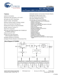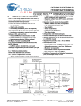
1
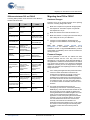
AN4078 Migrating From EZ-USB® FX2™ to EZ-USB FX2LP™ Author: Anand Srinivasan Associated Project: No Associated Part Family: CY7C68013A/14A/15A/16A Software Version: None Related Application Notes: None ® AN4078_C provides details on how to migrate an EZ-USB FX2 based design to EZ-USB FX2LP based design. It highlights the differences between the EZ-USB FX2LP™ and EZ-USB FX2™. It also provides a brief description of the whole product support collateral available for development work with FX2LP. Contents Introduction Introduction .......................................................................1 Difference between FX2 and FX2LP ............................2 Migrating from FX2 to FX2LP ............................................2 Hardware Changes ......................................................2 Firmware Changes .......................................................2 Details of the Hardware Changes .....................................3 Changes to Crystal Specification ..................................3 Minimum Reset Time....................................................4 VCC Ramp-up Time .......................................................4 Changes on AVCC/AGND Pin Functionality.................4 Details of Firmware Changes ............................................4 Disabling High-speed Chirp via EEPROM Config Byte 4 Automatic Disconnect and Reconnect on Hard Reset ..5 Expanded Code/Data RAM ..........................................5 Zero-length INPackets with No Firmware Intervention and Data PID Sequencing for ISO Transfers................5 Feature Enhancements .....................................................6 Lower Power ................................................................6 Enabling Pull-up on D+.................................................6 FIFO Address Lines Hold Time for Asynchronous Write .....................................................6 ECC Generation on GPIF data .....................................6 Package Changes ........................................................7 EZ-USB FX2LP Whole Product Support Collateral ...........7 Development Tool ........................................................7 Documentation .............................................................7 Summary ...........................................................................8 Worldwide Sales and Design Support ............................. 10 The EZ-USB FX2LP (CY7C68013A) is a next-generation USB high-speed controller. EZ-USB FX2LP enhances the functionality of the EZ-USB FX2 (CY7C68013) while minimally effecting existing designs. This application note serves two purposes: www.cypress.com 1. Assist in migrating existing EZ-USB FX2 (also referred to as FX2 in this application note) applications to EZUSB FX2LP (also referred to as FX2LP in this application note). 2. Assist the designers familiar with FX2 in creating FX2LP based applications. A summary of the main items to consider while replacing the FX2 in an existing application with an FX2LP part is provided. The changes are categorized into required essential changes for all FX2LP applications migrating from FX2 and other applications based changes that might be required in your application due to additional enhanced feature in FX2LP. Document No. 001-42079 Rev. *D 1 Migrating From EZ-USB FX2™ to EZ-USB FX2LP™ Difference between FX2 and FX2LP Migrating from FX2 to FX2LP Following table provides a brief overview of the difference between FX2 and FX2LP. Hardware Changes FX2 FX2LP Crystal load capacitor 20 to 33pF 12pF Minimum Reset Time 1.91ms 5ms Vcc Ramp-up time - at least 200 s with ramp rate of 18 V/ms AVCC/AGND pins - 2 additional AVCC/AGND pins Operates in fullDisabling highspeed, can Operates only in speed chirp through renumerate as highFull-speed EEPROM speed through firmware modification RESET# functionality Pull-up on D+ present pull-up on D+ even when RESET# disabled when asserted RESET# asserted Internal RAM 8 kB 16 kB Isochronous Zerolength packet (ZLP) support Does not send ZLP when no data available in SIE in response to isochronous IN request Capable of sending ZLP when no data available in SIE in response to isochronous IN request Power Moderate power (260mA maximum) Lower power (85mA maximum) Pull-up on D+ line Comes up enabled during power-up Comes up disabled during power-up FIFO address holdtime for Slave FIFO asynchronous write 70 ns 10 ns ECC generation on GPIF data Not-supported Supported www.cypress.com Following are a list of required changes when replacing the FX2 in a existing design with FX2LP: Make sure to replace the crystal with the appropriate load capacitors. The FX2LP requires a crystal with load capacitors of 12 pF. Make sure that the reset is held for at least 5 ms. Changes on AVCC/AGND pin functionality (see Changes on AVCC/AGND Pin Functionality on page 4). Make sure that the VCC ramp-up time is at least 200 s with a ramp rate of 18 V per millisecond. Note After installing CY3684 EZ-USB FX2LP Development Kit, the hardware collateral of the kit available at location C:\Cypress\USB\Hardware (Location varies based on installation) can be used as a reference to develop the board. Firmware Changes As next generation of the FX2, the FX2LP has some enhanced features that the user may want to take advantage of or may decide to simply disregard. Based on the application’s needs these enhancements in the FX2LP may require some changes in the designer’s FX2-based application. Following is a list of things that the designer needs to be informed when replacing the FX2 in a existing design with FX2LP. Is the existing FX2 application bus-powered and does it have the double enumeration workaround for meeting the unconfigured current limit of 100 mA. If so, set the control bit of the EEPROM to 0 (chip enabled) as the workaround is not required anymore. The FX2LP meets the 100-mA current requirement for unconfigured current. You may opt to either leave in or remove the double enumeration workaround in the firmware. The FX2LP automatically disconnects and subsequently reconnects on a hard reset (asserting RESET# pin). If the FX2 firmware has the 8051 do the disconnect and reconnect manually by setting and clearing DISCON bit of the USBCS register on a hard reset, it is not required anymore. Based on your application’s needs, when porting the same firmware to FX2LP, you may opt to either leave in or remove the code that does this disconnect and reconnect manually. This needs to be evaluated on an application basis and the effects (if any) on the system as a whole on disconnecting and reconnecting twice (if the 8051 code is left in the firmware ported to FX2LP). Document No. 001-42079 Rev. *D 2 Migrating From EZ-USB FX2™ to EZ-USB FX2LP™ FX2LP has internal memory from 0x0000 to 0x3FFFF as opposed to FX2 that has internal memory from 0x0000 to 0x1FFFF. Check the code location to make sure whether the existing FX2 application uses memory mapped ROM (any nonvolatile memory) or memory mapped I/O within the address space of 0x2000 to 0x3FFF. If so, they must be mapped to new locations and the firmware should be re linked as the FX2LP accesses the internal memory that is not the intended access method of the end application. In the limited number of designs that require this change, just a logic change to an FPGA or programmable logic array for hardware memory decoding and changing the target location of the external code within the compiler/linker is needed. If the existing FX2 design has RAM at this location (0x2000 to 0x3FFF), no changes are required while replacing the part with FX2LP. If the FX2 application use high-bandwidth Isochronous IN transfer, and if it has a workaround (on the host end or the device end) for handling the possible occurrence of a scenario of data PID mismatch: additional hardware, external logic, or software on the host end to handle the scenario, then you may consider removing the additional logic/code as the FX2LP has resolved this data PID mismatch issue. You may also choose to not remove the designed workaround for ease of drop-in replacement with FX2LP Note While changing components such as the USB controller (FX2 to FX2LP), the USB-IF requires a rerun of certification test. The following section provides details on the specifications on every change that is mentioned earlier. Details of the Hardware Changes An overview of the essential hardware changes/additions in the FX2LP are listed below: 24 MHz +100 ppm Parallel resonant Fundamental mode 500 W drive level 12-pF (5% tolerance) load cap One of the parts we recommend is one from ECS Inc. International: ECS-240-20-4. The above specification must be taken into consideration while selecting both the load capacitors and the crystal. Using a different crystal load capacitance with a crystal specified for 12 pF is expected to have some effect on the frequency shift. It is recommended that the designer always make sure that the power dissipated by the crystal is within the crystal manufacturer’s specifications. Overdriving the crystal may damage the crystal. See the specific crystal manufacturer’s recommendations. An article on crystal design and selection from Ecliptek's site states the following: “The rate of aging is typically greatest during the first 30 to 60 days after which time the aging rate decreases. The following factors effect crystal aging: adsorption and desorption of contamination on the surfaces of the quartz, stress relief of the mounting and bonding structures, material outgassing, and seal integrity.” One of the effects of over-driving the crystal out of its specified conditions may be aging of the crystal that is expected to result in frequency shift. From speaking to various crystal manufacturers, we have been informed that the majority of the shift due to aging usually occurs in the first 45–60 days or so. In general, it is recommended that a designer always make sure that the power dissipated by the crystal is within the crystal manufacturer’s specifications. Overdriving the crystal 'may' have adverse effects on the crystal performance and accuracy. It is also recommended that the user refer to the crystal manufacturer’s recommendations on the various effects of driving a crystal beyond its specified values. Changes to crystal specification Minimum reset time VCC ramp-up time Changes to AVCC/AGND Pin Functionality Changes to Crystal Specification With the use of FX2LP one change is required. When a crystal is used in the design, for proper operation the load capacitance of the crystal must change. This affects both the load capacitors and the crystal being used. The CY7C68013 requires a crystal with load capacitors that are between 20 pF and 33 pF. The CY7C68013A requires a crystal with load capacitors of 12 pF. If redesigning an FX2 application with FX2LP, the crystal must change to a www.cypress.com load capacitance of 12 pF, and the matching load capacitors must change to 12 pF. This is a requirement of all designs using FX2LP. Following is the spec on the crystal: Using a 16-pF or 20-pF crystal or any other standard load capacitance, may work as indicated by the discussions we have had with various crystal manufacturers. But using this is at the customer’s discretion as the FX2LP part was only tested and designed for a 12-pF, 24-MHz crystal. Please consult with the specific crystal manufacturer for information on the various effects of driving a crystal beyond its specified values. When a crystal is used in the design using FX2LP, Cypress recommends that for proper Document No. 001-42079 Rev. *D 3 Migrating From EZ-USB FX2™ to EZ-USB FX2LP™ operation the load capacitance of the crystal should be 12 pF. Disabling High-speed Chirp via EEPROM Config Byte Minimum Reset Time During power-on sequence, the operating speed of the FX2 device defaults to high-speed. The FX2 device has the capability of disabling the high-speed chirp state machine using the Cypress internal register CT1. The 8051 can set or clear bit 1 of the CT1 register anytime. On re-enumeration (disconnecting and then reconnecting) the FX2 device enumerates with the chirp state machine disabled if this bit of the CT1 register is set to 1. Therefore, on a disconnect event followed by a re-connect, the device re-enumerates as a full-speed only device. The minimum reset time speed for the FX2LP part is 5 ms. The FX2 was designed with a minimum reset time of 1.91 ms. VCC Ramp-up Time To obtain the power savings, the FX2LP parts use a core that is powered from 1.8 V. To maintain common power sources with the FX2LP silicon, this voltage is derived from the 3.3 V input. To properly power the internal regulator the 3.3 V input must have a limit on the power ramp-up rate. This means the input must turn on to a valid voltage (3.0 V to 3.6 V) over a 200-s period. This equates to an 18 V per/ms ramp rate. Powering up the input too quickly latches the internal regulator and cause issues in powering up the core. Many 3.3 V regulators have turn-on times that are long enough to properly power-up the internal regulator. One such regulator from Linear Technology is the LT1763CS8-3.3. Changes on AVCC/AGND Pin Functionality There are no major changes as far the PCB is concerned. Both FX2 and FX2LP run on a single 3.3 V supply. There are two additional AVCC/AGND pins on the FX2LP that can be rerouted on the PCB to provide additional filtering. These two additional pins exist in the 56-, 100-, and 128pin packages. For the 128-pin TQFP package, AVCC is pin 17 (was VCC on the FX2), and AGND is pin 20 (was GND on the FX2). Pin 17 of the FX2LP128 pin package does not need a duplicate of the pin 10 AVCC filter network. It can be wired in parallel to pin 10. The FX2LP can use the same filter network as the FX2 for AVCC. The FX2LP analog ground (pin 20 in 128 pin package) does not need to be isolated. It can be connected to the digital ground. Other changes made to the chip do not affect all designs. Details of Firmware Changes This section highlights major improvements and changes in FX2LP that may affect the older FX2 design while migrating to FX2LP. Most of these do not affect your design. The information given here is the evaluation on how it may affect your application design. An overview of these features is listed as follows: Disabling high-speed chirp via EEPROM config byte Automatic Disconnect and reconnect on a hard reset Expanded internal code/data RAM The chirp state machine can also be disabled on powerup, by setting bit 7 of the configuration byte of the EEPROM. During power-up sequence, the core copies this bit setting to bit 1 of the CT1 register and the device enumerates as a full-speed device. After enumerating as a full-speed device, the 8051 may enable the chirp state machine anytime by clearing bit 1 of the CT1 register. On re-enumeration the same device enumerates as a highspeed device. In the case of FX2LP, the device also defaults to a highspeed mode of operation: bit 1 of the CT1 register defaults to 0. After the device has powered-up with the chirp state machine enabled (default), it can be switched to a different mode of operation by having the 8051 change bit 1 of the CT1 register. If no EEPROM is used, the device operates in its default high-speed mode. If using an EEPROM, the chirp state machine status is determined by the setting of bit 7 of the configuration byte of the EEPROM. The behavior of the FX2LP chirp state machine is different than the FX2 when bit 7 of the configuration byte of the EEPROM is set to 1 (chirp state disabled on power-up). The CT1 register and the EEPROM control bit (bit 7 of the configuration byte) behave differently in FX2LP than in FX2. In FX2, if the EEPROM control bit that forces USB full-speed operation is set, FX2 comes up in full-speed mode, and upon re-enumeration FX2 is capable of reenumerating on the USB bus in high-speed mode (if the 8051 has cleared bit 1 of the CT1 register to enable highspeed mode). In the case of FX2LP, if the full-speed control bit of the EEPROM is set, the device ONLY comes up in full speed mode, even after USB re-enumeration. Setting or clearing this bit by the 8051 has no effect on enabling or disabling the chirp state machine when bit 7 of the configuration byte of the EEPROM is set to 1. If it is set to 0, FX2LP behaves the same as the FX2. In other words when bit 7 of configuration byte is set to 0 (chirp enabled) the FX2LP comes up in high-speed mode and the 8051 may switch the mode by changing bit 1 of CT1 register anytime followed by a disconnect and reconnect event. Zero-length packets with no firmware intervention and Data PID sequencing in isochronous IN transfers www.cypress.com Document No. 001-42079 Rev. *D 4 Migrating From EZ-USB FX2™ to EZ-USB FX2LP™ If the existing FX2 application is bus powered and uses the double enumeration sequence (that is a recommended workaround) to meet the unconfigured current requirements of the USB-IF compliance test, then the application does not behave the same when replaced with the FX2LP. If replacing the part with FX2LP, when the device enumerates with the high-speed chirp disabled (control bit of the configuration byte of the EEPROM set), on renumeration, the device fails to enumerate as a highspeed device even though the 8051 had cleared bit 1 of the CT1 register. The full-speed mode trick upon initial plugin FX2 was done to get the unconfigured power-down to the 100-mA range to meet the USB specification. As FX2LP power is 50–60 mA maximum, not meeting the unconfigured current limit when using the device as bus powered is no longer an issue, there is no need to set this control bit in the EEPROM anymore. The workaround is not required anymore. Just have the FX2LP application enumerate in USB high speed mode from the start. For an FX2 bus-powered application that uses double enumeration sequence to behave the same when replaced with FX2LP, all you need to do is set the control bit of the EEPROM to 0 (chirp enabled) and can leave the firmware as is with the double enumeration workaround code in it. Automatic Disconnect and Reconnect on Hard Reset The FX2LP has an enhanced capability of disconnecting and reconnecting on a hard reset, when the RESET# is asserted by the external peripheral. The FX2 does not cause a disconnect on a hard reset (RESET# asserted). On releasing the reset the FX2 no longer responds to the host since it does not have a valid address anymore. To resume communication with the host the 8051 must cause a disconnect and a reconnect by setting DISCON bit of the USBCS register and subsequently clearing. On a reconnect event the host issues a SET_ADDRESS request and re-enumerate the device. In the case of an FX2LP, the device does a disconnect and a reconnect automatically on a hard reset. When the RESET# is asserted, the FX2LP resets the FNADDR (function address) register to 0x00. On releasing the reset# the FX2LP automatically does a disconnect followed by a reconnect. If using FX2LP the 8051 does not need to be programmed to do the disconnect and reconnect by setting and clearing the DISCON bit manually. Expanded Code/Data RAM The FX2LP has 16 Kbytes of internal Code/Data RAM, where the FX2 had only 8 Kbytes. The additional RAM is located in the address space of 0x2000 to 0x3FFF. If the firmware of the existing design is completely internal to the www.cypress.com FX2, no changes are required to use the FX2LP. If the FX2 design had RAM at this location, no changes are required. The FX2LP accesses the internal RAM instead of the external RAM. If there was either memory mapped ROM (any nonvolatile memory) or memory mapped I/O within these locations, they must be mapped to new locations and the firmware should be re linked. In the limited number of designs that require this change, just a logic change to a FPGA or programmable logic array for hardware memory decoding and changing the target location of the external code within the compiler/linker is required. In most designs it is felt that the external memory map would not have used this location in memory. Less logic is required to locate the memory at higher locations and therefore it is believed that most designs would have used a higher address, such as 0x8000, to start the external memory. If this is the case, no modifications, other then the required crystal modifications, are required. Zero-length INPackets with No Firmware Intervention and Data PID Sequencing for ISO Transfers The FX2LP has the capability of sending a zero-length isochronous data packet (ZLP) when the host issues an IN token to an isochronous IN endpoint FIFO and the SIE does not have any data packets available. This feature is very useful when designing high-bandwidth isochronous applications. When an isochronous IN endpoint is configured for greater than one packet per microframe, there is a possibility of the core not having more than one packet available in a microframe. In this case, when the host issues an IN token, the FX2LP core sends a zero-length packet with the appropriate data PID automatically. Hence avoiding the occurrence of a scenario where the host may encounter a turnaround timeout error on not receiving any data when requesting more than one packet per microframe. In the Technical Reference Manual, register EPxISOINPKTS (x = Endpoint number) defines an additional bit called: ADDJ. This bit defaults to a zero value. In this condition, FX2LP operates the same as the FX2. The auto adjust (AADJ) feature was useful when designing with the FX2LP engineering samples provided at the early stages of the FX2LP development. These engineering samples did not have the ability to issue a zero-length isochronous packets automatically and hence were prone to running into a DATA PID mismatch scenario when dealing with high-bandwidth ISO IN transfer (please see the “Streaming Data Through Isochronous/Bulk Endpoints on EZ-USB FX2™ EZ-USB FX2LP™ AN4053” application note for further information on DATA PID mismatch issue). The auto adjust feature is a workaround to the data PID mismatch issue and to use Document No. 001-42079 Rev. *D 5 Migrating From EZ-USB FX2™ to EZ-USB FX2LP™ this workaround, the wMaxPacketSize that could be defined in the isochronous endpoint descriptor is limited to 1024 bytes. Feature Enhancements This section is for designers already familiar with the FX2 architecture who are creating a new application using FX2LP This section highlights additional (along with the essential and application based changes mention in the prior two sections) improvements and changes in FX2LP. An overview of the feature changes/additions in the FX2LP are listed as follows: Lower power Enabling pull-up on D+ FIFO address lines hold time for asynchronous write There is a minor difference with respect to when the internal logic enables the pull-up on D+ to signal an attach event to the host. In the case of the FX2, the pull-up on D+ is enabled on power-up. In the case of the FX2LP, the pull-up on D+ is enabled when the reset is released (in a deasserted state). On plug-in, the FX2 enables the pull-up on D+ signaling at attach event to the host. If the reset is held active for longer than 100 ms, an attach signal is sent to the host and the host begins its enumeration sequence (after 100 ms from when the attach is detected), while the FX2 is still held in reset. Section 7.1.7.3 (page 150) of the USB 2.0 specification, provides further information on the debounce interval (delta t3). While using the FX2 Cypress recommends that a reset time of 10 ms with an RC network of 100K/0.1 F be used. The FX2LP has a more flexible reset timing requirement. As the FX2LP enables the pull-up on the D+ after the RESET is deasserted, there really is no restriction on the reset timing as only the host receives an attach signal when the RESET is released. ECC generation on GPIF data Additional Package with more GPIOs (CY7C68015A/16A). Lower Power As far as the power source is concerned, the FX2LP uses a different process than the FX2. The FX2LP uses an internal 1.8 V regulator. The major result of this change is to reduce the power consumption of the chip. The lower current is obtained just by using the FX2LP with the required crystal modifications. This configuration meets all USB bus powered requirements of unconfigured current (100 mA) and suspend current (500 A). As a result of this lower power, to meet the unconfigured current limit, it is no longer necessary to use the double enumeration procedure where the device first enumerates in full-speed with a current draw below 100 mA and then disconnects and reconnects as a high-speed device. If an existing design uses this procedure the designer can remove the procedure in design. For new designs using FX2LP, there is no concern as the part does meet the 100-mA limitation requirement for unconfigured current while operating in either full or high speed. www.cypress.com Enabling Pull-up on D+ FIFO Address Lines Hold Time for Asynchronous Write In the case of an FX2 device, when operating in slave FIFO mode in an asynchronous interface, the minimum hold time (tFAH) for FIFO address lines (FIFOADR[1:0]) for a slave FIFO write operation is 70 ns, that is measured from the deasserting edge of SLWR. This has been improved and optimized to 10 ns when using the FX2LP parts. The FIFOADDR[1:0] lines hold time (tFAH) for a slave FIFO asynchronous write is speed for a minimum of 10 ns for the FX2LP. ECC Generation on GPIF data This is a new feature and does not affect existing designs. If ECC generation is to be added to an existing design there are additional registers that enable this function. The FX2LP can be configured to either calculate two separate 256-byte ECCs on two consecutive 256-byte blocks of data, or alternatively one single 512-byte ECC on a 512-byte block of data. After the 8051 resets the ECC calculation by writing any value to ECCRESET, the FX2LP calculates ECC on any data bytes that transfer across the GPIF or Slave FIFO interface. The FX2LP stops ECC calculation after all 512 bytes have been processed and it waits for a new ECC reset from the 8051 before it commences any new calculations. Document No. 001-42079 Rev. *D 6 Migrating From EZ-USB FX2™ to EZ-USB FX2LP™ The additional registers for this function are: ECCCFG Configuration register (256/512) ECCRESET Reset ECC-byte registers to zero ECC1B0 This is the second eight bits of the line parity on the first 256byte block or the 512-byte block. ECC1B1 Lower eight bits of line parity on first 256-byte block or lower eight bits of line parity on 512byte block. ECC1B2 This is the 6-bit column parity on first 256-byte block or 6-bit column parity on and upper two bits of line parity for 512byte block. ECC2B0 This is the second eight bits of the line parity. on the second 256-byte block ECC2B1 Lower eight bits of line parity on second 256-byte block ECC2B2 This is the 6-bit column parity on the second 256-byte block (For column and line parity see Smart media Specification.) See Technical Reference Manual for check/correct sample code. Package Changes Additional options have been made available in the packaging of the FX2LP part. Additional configurations are available in the 56-pin packages. These configurations allow for two additional GPIO pins. These parts are the part number CY7C68015A/CY7C68016A, available in both a QFN and a SSOP package. In CY7C68015A/16A, IFCLK and CLKOUT pins are replaced by PE0 and PE1 respectively. The effect of this change on the design has to be considered while replacing FX2 (56-pin QFN package) with CY7C68015A/16A. As in FX2, all FX2LP parts are available in lead-free packages. The following table lists the FX2 parts and the respective FX2LP part that may be used to replace the FX2. Besides the packages that are specified, FX2LP also has a VFBGA 56-pin package (CY7C68013A-56BAXC and CY7C68014A-56BAXC). CY7C68014A and CY7C68016A are Ideal for batterypowered applications as they have an ultra-low suspend current of 100 A (typical). CY7C68013A and CY7C68015A, that have a low suspend current of 300 A (typical), are ideal for non-battery powered (self or bus powered) applications. EZ-USB FX2 Part Number CY7C68013-56PVC or CY7C6801356PVXC EZ-USB FX2LP Part Number CY7C68013A-56PVXC or CY7C68013A-56PVXI or CY7C68014A-56PVXC Package Description 56-pin SSOP CY7C68013-56LFC or CY7C68013A-56LTXC or 56-pin QFN CY7C68013-56LFXC CY7C68013A-56LTXCT or CY7C68013A-56LTXI or CY7C68014A-56LTXC CY7C68013-100AC or CY7C68013100AXC CY7C68013A-100AXC or CY7C68013A-100AXI or CY7C68014A-100AXC 100-pin TQFP CY7C68013-128AC or CY7C68013128AXC CY7C68013A-128AXC or CY7C68013A-128AXI or CY7C68014A-128AXC 128-pin TQFP EZ-USB FX2LP Whole Product Support Collateral Development Tool The EZ-USB FX2LP has a development kit similar to that of the EX-USB FX2. The part number for this kit is CY3684. The development kit for the FX2LP contains a development board, cables, documentation and a development CD. The CD has electronic copies of the Technical Reference Manual, the data sheet, schematics and gerbers for the development board, firmware examples, drivers (CyUSB.sys)and evaluation version of the Keil’s Vision2 Compiler. Documentation 1. EZ-USB Technical Reference Manual 2. CY7C68013A/14A/15A/16A Datasheet 3. GETTING STARTED WITH FXLP™ Application note 4. HIGH-SPEED USB PCB RECOMMENDATIONS – AN1168 5. EZ-USB FX2LP(TM)/ AT2LP(TM) RESET POWER CONSIDERATIONS – AN064 LAYOUT AND Go to www.cypress.com to download the latest version of the product collateral. . www.cypress.com Document No. 001-42079 Rev. *D 7 Migrating From EZ-USB FX2™ to EZ-USB FX2LP™ Summary This application note has introduced the differences between the FX2 and the FX2LP. As discussed in this application note, the only required change when using the FX2LP in place of the FX2 is the alteration of the crystal load capacitors and the load capacitance of the crystal. With exception of the load capacitance on the crystal, the crystal for the FX2LP contains the same requirements as that for the FX2. Additional features are also highlighted, but are defaulted to function as the FX2 would. This enables use of FX2LP in prior designs with minimal or none at all changes to the firmware. Due to the increased memory within the FX2LP, a limited number of designs may require a memory map change. About the Author Name: Anand Srinivasan Title: Applications Engineer Sr Contact: [email protected] As with Cypress’s FX2, the FX2LP is made available with world-class development tools and software support. Visit www.cypress.com for more device details and data sheet information. www.cypress.com Document No. 001-42079 Rev. *D 8 Migrating From EZ-USB FX2™ to EZ-USB FX2LP™ Document History ® Document Title: Migrating From EZ-USB FX2™ to EZ-USB FX2LP™ Document Number: 001-42079 Revision ECN Orig. of Change Submission Date Description of Change ** 1597504 SSJO/YIS 10/11/2007 Re-catalogued application note. *A 3149911 AASI 01/21/2011 Added content for clearer understanding on the memory map changes. Updated the application note with latest part number and collateral details. *B 3348476 AASI 08/18/2011 Changed “Essential Changes” in page 1 to “Hardware Changes” Changed “Application based Changes” in page 1 to “Firmware Changes” Changed “Details of Essential Changes” in page 2 to “Details of Hardware Changes” Changed “Details of Application based Changes” in page 3 to “Details of Firmware Changes *C 3475798 AASI 12/26/2011 Updated template according to current Cypress standards. Added Table showing difference between FX2 and FX2LP. Minor text edits. *D 3734331 PRJI 09/05/2012 Updated template. Changed application note number from AN4078_C to AN4078. www.cypress.com Document No. 001-42079 Rev. *D 9 Migrating From EZ-USB FX2™ to EZ-USB FX2LP™ Worldwide Sales and Design Support Cypress maintains a worldwide network of offices, solution centers, manufacturer’s representatives, and distributors. To find the office closest to you, visit us at Cypress Locations. PSoC® Solutions Products Automotive cypress.com/go/automotive psoc.cypress.com/solutions Clocks & Buffers cypress.com/go/clocks PSoC 1 | PSoC 3 | PSoC 5 Interface cypress.com/go/interface Lighting & Power Control cypress.com/go/powerpsoc cypress.com/go/plc Memory cypress.com/go/memory Optical Navigation Sensors cypress.com/go/ons PSoC cypress.com/go/psoc Touch Sensing cypress.com/go/touch USB Controllers cypress.com/go/usb Wireless/RF cypress.com/go/wireless Cypress Developer Community Community | Forums | Blogs | Video | Training Technical Support cypress.com/go/support In March of 2007, Cypress recataloged all of its Application Notes using a new documentation number and revision code. This new documentation number and revision code (001-xxxxx, beginning with rev. **), located in the footer of the document, will be used in all subsequent revisions. EZ-USB is a registered trademark and EZ-USB FX2 and EZ-USB FX2LP are trademarks of Cypress Semiconductor Corporation. All other trademarks or registered trademarks referenced herein are the property of their respective owners. Cypress Semiconductor 198 Champion Court San Jose, CA 95134-1709 Phone Fax Website : 408-943-2600 : 408-943-4730 : www.cypress.com © Cypress Semiconductor Corporation, 2007-2012. The information contained herein is subject to change without notice. Cypress Semiconductor Corporation assumes no responsibility for the use of any circuitry other than circuitry embodied in a Cypress product. Nor does it convey or imply any license under patent or other rights. Cypress products are not warranted nor intended to be used for medical, life support, life saving, critical control or safety applications, unless pursuant to an express written agreement with Cypress. Furthermore, Cypress does not authorize its products for use as critical components in life-support systems where a malfunction or failure may reasonably be expected to result in significant injury to the user. The inclusion of Cypress products in life-support systems application implies that the manufacturer assumes all risk of such use and in doing so indemnifies Cypress against all charges. This Source Code (software and/or firmware) is owned by Cypress Semiconductor Corporation (Cypress) and is protected by and subject to worldwide patent protection (United States and foreign), United States copyright laws and international treaty provisions. Cypress hereby grants to licensee a personal, non-exclusive, non-transferable license to copy, use, modify, create derivative works of, and compile the Cypress Source Code and derivative works for the sole purpose of creating custom software and or firmware in support of licensee product to be used only in conjunction with a Cypress integrated circuit as specified in the applicable agreement. Any reproduction, modification, translation, compilation, or representation of this Source Code except as specified above is prohibited without the express written permission of Cypress. Disclaimer: CYPRESS MAKES NO WARRANTY OF ANY KIND, EXPRESS OR IMPLIED, WITH REGARD TO THIS MATERIAL, INCLUDING, BUT NOT LIMITED TO, THE IMPLIED WARRANTIES OF MERCHANTABILITY AND FITNESS FOR A PARTICULAR PURPOSE. Cypress reserves the right to make changes without further notice to the materials described herein. Cypress does not assume any liability arising out of the application or use of any product or circuit described herein. Cypress does not authorize its products for use as critical components in life-support systems where a malfunction or failure may reasonably be expected to result in significant injury to the user. The inclusion of Cypress’ product in a life-support systems application implies that the manufacturer assumes all risk of such use and in doing so indemnifies Cypress against all charges. Use may be limited by and subject to the applicable Cypress software license agreement. www.cypress.com Document No. 001-42079 Rev. *D 10