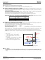
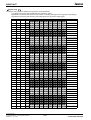
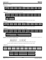
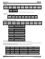
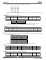
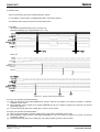
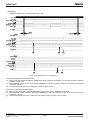
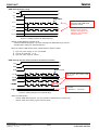
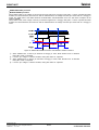
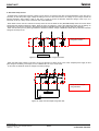
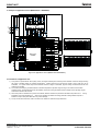
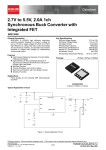
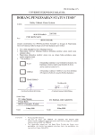
1
Datasheet LED Drivers for LCD Backlights White LED Diver for Backlight of Medium/Large-sized LCDs BD9271KUT General Description BD9271KUT is a white LED diver used on backlight of Medium/Large-sized LCDs. This IC can achieve dimming function by SPI control. And through the SPI correspondence, it can set the ON/OFF of each switch, analog dimming and etc. The signals of PWM dimming can set the frequency, ON time and delay of PWM by inputting the external signals to the register. BD9271KUT has equipped several protection functions to deal with the abnormal states, including LED OPEN protection, LED SHORT protection, external current setting resistance SHORT protection, external MOS transistor SHORT protection, etc. So it can be used in a wide output voltage range and various load conditions. Key Specifications ■ VCC power supply range: 9.0V~35.0V ■ DVDD power supply range: 3.0V~3.6V ■ CLK frequency setting range: 100~10000kHz ■ Operating Circuit current range: 2.4mA(typ.) ■ Operating temperature range: -40℃~+85℃ Features ■ 16-ch constant current driver (external FET(NMOS)is equipped.) ■ LED voltage can be set externally. ■ PWM dimming and Analogue dimming can be controlled by SPI. ■ LED Abnormal operation detection circuit (OPEN protection/ SHORT protection) is equipped. ■ LED SHORT protection detection voltage is adjustable (LSP terminal) ■ LED SHORT protection detection CH ■ FAIL INDICATION function is equipped by ERR_DET terminal. ■ 3 lines serial interface ■ Package: TQFP64UM Package TQFP64UM Pin Pitch W(Typ.) D(Typ.) H(Max.) 9.00mm×9.00mm×1.20mm 0.4mm Applications TV, PC display Other LCD backlight Figure 1. TQFP64UM Typical Application Circuit Figure 2. Typical Application Circuit ○Product structure:Silicon monolithic integrated circuit www.rohm.com © 2013 ROHM Co., Ltd. All rights reserved. TSZ22111・14・001 ○This product is not designed protection against radioactive rays 1/34 TSZ02201-0F1F0C100260-1-2 27.Feb.2015 Rev.004 Datasheet BD9271KUT Absolute Maximum Ratings(Ta=25℃) Parameter Symbol Ratings Unit VCC 36 V Power Supply Voltage at digital part DVDD 4.5 V STB Terminal Voltage VSTB VCC V Power Supply Voltage VD1~VD16 D1~16 Terminal Voltage VERR_DET ERR_DET Terminal Voltage S1~S16, G1~G16, VREF5V, LSP, VS1~S16, VG1~VG16,VREF5V,VLSP, VCOMP1,VCOMP2 COMP1, COMP2 Terminal Voltage CS, CLK, DI, DO, VSYNC, HSYNC Terminal VCS,VCLK,VDI,VDO,VVSYNC,VHSYNC Voltage Pd Power Dissipation 40 V VCC V 7 V 4.5 V (Note 1) 1.37 W Operating Temperature Range Topr -40~+85 ℃ Storage temperature range Tstg -55~+150 ℃ Tjmax 150 ℃ Junction temperature (Note 1)When Ta = 25°C or higher, power dissipation is down with 11.0mW/°C (when a 70 mm x 70 mm x 16 mm 1-layer glass epoxy board is mounted). Operation range(Ta=25℃) Parameter Power source voltage Symbol Limits Unit VCC 9.0~35.0 V Power Supply Voltage at digital part DVDD 3.0~3.6 V CLK oscillation frequency setting range fCLK 100~10000 kHz fVSYNC 80 ~ 1000 Hz VSYNC input oscillation frequency range VLSP 0.8 ~ 3.0 V LSP terminal input voltage The operating ranges above are acquired by evaluating the IC separately. Please take care when set the IC in applications. 48 47 46 45 44 43 42 41 40 39 38 37 36 35 34 33 D16 S16 G15 D15 S15 G14 D14 S14 G13 D13 S13 G12 D12 S12 G11 Package outline drawing G16 Block diagram TQFP64UM (TOP VIEW) Marking G1 D1 S1 G2 D2 S2 G3 D3 S3 G4 D4 S4 G5 D5 S5 G6 1 2 3 4 5 6 7 8 9 10 11 12 13 14 15 16 BD9271 Lot No. 1Pin Mark Figure 3. Pin Configuration www.rohm.com © 2013 ROHM Co., Ltd. All rights reserved. TSZ22111・15・001 Figure 4. Marking Diagram 2/34 TSZ02201-0F1F0C100260-1-2 27.Feb.2015 Rev.004 Datasheet BD9271KUT Electrical characteristics (unless otherwise specified, Ta = 25°C, VCC = 12V, STB=3V) Item Symbol Standard value Minimum 【Whole device】 Operating circuit Icc - current Stand-by circuit IST - current 【VREF5V block】 VREF5V output VREF5 4.95 voltage VREF5V Maximum IREF5 15 output current 【Error amplifier block】 COMP1,COMP2 ICOMPSINK 300 terminal sink current LED control voltage VLED 270 【UVLO block】 Operation power VUVLO_VCC 6.0 source voltage(VCC) hysteresis voltage VUHYS_VCC 150 (VCC) 【LED DRIVER block】 LED terminal current ⊿ILED -1.5 accuracy OPEN detection VOPEN 0.05 voltage SHORT detection VSHORT 4.5 voltage Upper resistance of divided LSP terminal RupLSP 1000 resistance Lower resistance of divided LSP terminal RdownLSP 250 resistance Error detection of current detection VRESSH 0.10 resistance 【STB block】 STB terminal HIGH STBH 2.0 voltage STB terminal LOW STBL -0.3 voltage STB terminal Pull REN 600 Down resistance 【FAIL block】 ERR_DET terminal RFAIL 55 ON resistance 【LOGIC input (CS, CLK, DI, HSYNC, VSYNC)】 0.7× Input High voltage VINH DVDD Unit Condition Standard Maximum 2.4 5.0 mA LED1-16 OFF 200 500 μA STB=0V 5.00 5.05 V IO=0mA - - mA - - µA 300 330 mV 7.0 8.0 V 300 600 mV - 1.5 % ILED=100mA 0.10 0.15 V VD=SWEEP DOWN 5.0 5.5 V VD=SWEEP UP - - kΩ LSP=0V - - kΩ LSP=5V 0.15 0.20 V - VCC V - 0.8 V 1000 1800 kΩ VIN=3V( STB ) 110 220 Ω IERR_DET=5mA - VCOMP=0.5V VCC=SWEEP UP VCC=SWEEP DOWN LEDREF default DVDD +0.3 0.3× DVDD 5 µA VIN=3.3V V Input Low voltage VINL -0.3 - V Input inflow current IIN1 -5 0 Output High voltage VOUTH DVDD -0.6 DVDD -0.3 - V IOL=-1mA Output Low voltage VOUTL - 0.19 0.60 V IOL=1mA 【LOGIC output (DO) 】 www.rohm.com © 2013 ROHM Co., Ltd. All rights reserved. TSZ22111・15・001 3/34 TSZ02201-0F1F0C100260-1-2 27.Feb.2015 Rev.004 Datasheet BD9271KUT Terminal No., Name, and Function Function No. Function No. Terminal No. Terminal Function 1 G1 CH1 NMOS gate terminal 17 D6 CH6 NMOS drain terminal 33 G11 CH11 NMOS gate terminal 49 VREF5V 5V regulator output terminal 2 D1 CH1 NMOS drain terminal 18 S6 CH6 NMOS source terminal 34 S12 CH12 NMOS source terminal 50 LSP SHORT detection setting terminal 3 S1 CH1 NMOS source terminal 19 G7 CH7 NMOS gate terminal 35 D12 CH12 NMOS drain terminal 51 VCC Power source terminal G2 CH2 NMOS gate terminal D7 CH7 NMOS drain terminal G12 CH12 NMOS gate terminal 52 STB Enable terminal D2 CH2 NMOS drain terminal S7 CH7 NMOS source terminal S13 CH13 NMOS source terminal 53 GND GND terminal 6 S2 CH2 NMOS source terminal 22 G8 CH8 NMOS gate terminal 38 D13 CH13 NMOS drain terminal 54 COMP2 ERROR AMP output (CH9~16) 7 G3 CH3 NMOS gate terminal 23 D8 CH8 NMOS drain terminal 39 G13 CH13 NMOS gate terminal 55 COMP1 ERROR AMP output (CH1~8) 8 D3 CH3 NMOS drain terminal 24 S8 CH8 NMOS source terminal 40 S14 CH14 NMOS source terminal 56 DGND Digital GND terminal 9 S3 CH3 NMOS source terminal 25 S9 CH9 NMOS source terminal 41 D14 CH14 NMOS drain terminal 57 CS Chip select terminal 10 G4 CH3 NMOS gate terminal 26 D9 CH9 NMOS drain terminal 42 G14 CH14 NMOS gate terminal 58 CLK Clock input terminal 11 D4 CH4 NMOS drain terminal 27 G9 CH9 NMOS gate terminal 43 S15 CH15 NMOS source terminal 59 DI DATE input terminal S4 CH4 NMOS source terminal S10 CH10 NMOS source terminal D15 CH15 NMOS drain terminal 60 DO DATE output terminal 13 G5 CH5 NMOS gate terminal 29 D10 CH10 NMOS drain terminal 45 G15 CH15 NMOS gate terminal 61 VSYNC VSYNC signal terminal 14 D5 CH5 NMOS drain terminal 30 G10 CH10 NMOS gate terminal 46 S16 CH16 NMOS source terminal 62 HSYNC HSYNC signal terminal 15 S5 CH5 NMOS source terminal 31 S11 CH11 NMOS source terminal 47 D16 CH16 NMOS drain terminal 63 ERR_DET Abnormal detection output terminal 16 G6 CH6 NMOS gate terminal 32 D11 CH11 NMOS drain terminal 48 G16 CH16 NMOS gate terminal 64 DVDD Digital Power source terminal No. 4 5 12 Terminal Terminal 20 21 28 www.rohm.com © 2013 ROHM Co., Ltd. All rights reserved. TSZ22111・15・001 36 37 44 4/34 Function TSZ02201-0F1F0C100260-1-2 27.Feb.2015 Rev.004 Datasheet BD9271KUT Internal Equivalent Circuit Diagram G1~G16 D1~D16 S1~S16 VREF5V S1~S16 10kΩ GND VREF5V GND GND LSP STB VREF5V 2MΩ LSP STB 500k 1M 500kΩ GND GND GND GND GND COMP1, COMP2 CS, CLK, DI DO DVDD DVDD DVDD DVDD CS,CLK,DI 10kΩ DO 50Ω DGND DGND GND DGND VSYNC, HSYNC ERR_DET Figure 5. Pin ESD Type www.rohm.com © 2013 ROHM Co., Ltd. All rights reserved. TSZ22111・15・001 5/34 TSZ02201-0F1F0C100260-1-2 27.Feb.2015 Rev.004 Datasheet BD9271KUT Block Diagram DVDD VREF5V VREF5V STB LSP ERR_DET VCC VREF PWM1 FB1 + UVLO REG FB16 GND OPEN DET SHORT DET - MS1 UVLO DVDD MS1 DI FPGA MS16 CLK CS SPI I/F D1 PWM2 + - G1 MS2 D2 + - MS16 register PWM DUTY CONTROL PWM1 PWM16 CH1 S1 PWM16 LED_ref DAC VSYNC (ON timming) HSYNC (clock) MOS SHORT DET Protect logic DO DGND RES SHORT DET LED16_dr_moni LED LED1_dr_moni LED G2 CH2 S2 EAMP_ref DAC FB1 LED1_dr_moni FB2 LED2_dr_moni D16 FB1 + FB8 + - FB9 + FB16 + - G16 CH16 S16 FB16 COMP2 LED16_dr_moni COMP1 Figure 6. Block Diagram www.rohm.com © 2013 ROHM Co., Ltd. All rights reserved. TSZ22111・15・001 6/34 TSZ02201-0F1F0C100260-1-2 27.Feb.2015 Rev.004 Datasheet BD9271KUT Typical Performance Curves 400 5.0 4.5 350 4.0 300 3.5 3.0 Icc [mA] IST [uA] 250 200 2.5 2.0 150 1.5 100 1.0 50 0.5 0 0.0 9 13 17 21 25 29 33 9 VCC [V] 13 17 21 25 29 33 VCC [V] Figure 8. Operating Current (Icc) [mA] vs. VCC[V] (LED1-16 OFF) Figure 7. Stand-by Current (IST) [µA] vs. VCC[V] 5.5 5.4 5.3 VREF5V [V] 5.2 5.1 5.0 4.9 4.8 4.7 4.6 4.5 9 13 17 21 25 29 33 VCC [V] Figure 9. VREF5V[V] vs. VCC[V] www.rohm.com © 2013 ROHM Co., Ltd. All rights reserved. TSZ22111・15・001 7/34 TSZ02201-0F1F0C100260-1-2 27.Feb.2015 Rev.004 Datasheet BD9271KUT Pin Function Descriptions G1-G16 (1,4,7,10,13,16,19,22,27,30,33,36,39,42,45,48PIN) External FET gate driving terminal of LED constant current driver, operating range : 0~5V. S1-S16 (3,6,9,12,15,18,21,24,25,28,31,34,37,40,43,46PIN) Connect to external FET’s source terminal of LED constant current driver. Through the operations of constant current driver, all CHs of S1-S16 terminals are outputted the set voltages at addresses of 02h, 03h, and S1-S16 proceed the constant current operation. By monitoring the voltage of this terminal, the external resistance SHORT detection of each CH and external MOS SHORT during Drain-Source detection proceed. When Dimming=HIGH, external resistance SHORT detection proceeds, and output the errors. When Dimming=LOW, external MOS Drain-Source SHORT detection proceeds, and output the errors. The detection voltage of Sx pin for RESSHORT, MOSSHORT protection corresponds to the register value of 02h, 03h LEDREF (the normal operation voltage of Sx pin). Please refer to the condition of protections. LEDREF[11:0] Abnormal detection Normal operation voltage voltage 000h - 0CDh 0.05V 0.1V 800h - FFFh 0.50V 1.0V 266h(default) 0.15V 0.3V D1-D16 (2,5,8,11,14,17,20,23,26,29,32,35,38,41,44,47PIN) At output terminal of LED constant current driver, drain of external FET is connected. By monitoring the voltage of this terminal, LED OPEN detection and LED SHORT detection of each terminal proceed. When Dimming=HIGH, if LED is in SHORT mode or OPEN mode, error signals are outputted. LED OPEN protection detected voltage ・・・0.1V(typ.) LED SHORT protection detected voltage・・・5.0V(typ.)・・・(It can be changed by setting the LSP terminal. Details are given in LSP Pin Description.) When Dimming = LOW, the abnormal state when Dimming = HIGH just before continues. In other words, when Dimming=HIGH and the abnormal state is detected, the error signal is still outputted even turned to Dimming=LOW. To prevent the mistake of detection caused by the time change of state, abnormal detection mask can be set at address of 04h. At D1~16 pin ① LED OPEN detection(when PWM=H) ② LED SHORT detection(when PWM=H) At S1~16 pin ③ RESISTOR SHORT detection(when PWM=H) ④ MOS SHORT detection(when PWM=L) are detected, then the error signals are outputted. Figure 10. LED Protected operation VREF5V (49PIN) The VREF5V pin is used to output power (5V) to the internal block of the IC and serves as a main power supply for the internal circuit of the IC. Install a ceramic capacitor as close to this pin as possible in order to stabilize the power supply voltage. www.rohm.com © 2013 ROHM Co., Ltd. All rights reserved. TSZ22111・15・001 8/34 TSZ02201-0F1F0C100260-1-2 27.Feb.2015 Rev.004 Datasheet BD9271KUT LSP (50PIN) A pin used for setting the LED SHORT protection detecting voltage. When LSP pin is in OPEN state, the voltage in inward of IC is 1V typ.(Set it in range of 0.8V~3.0V) When LED is lighting, if the voltage of D1~16 pin is higher than 「Voltage of LSP x 5 (V) 」(default 5V) the abnormal state of IC is detected. Because this pin has a high impedance, please connect a capacitor about 1000pF to remove the noise basically. REG VREF5V SHORT DET 2.0MΩ ー + + + + + … D1 D2 D3 D4 R1 LSP CLSP 500kΩ GND GND R2 GND D16 Figure 11. LSP Pin Internal Equivalent Circuit Diagram BSx Pin LED short detect voltage [V] In case of outputting a voltage to LSP by using the resistor divider circuit, REF5V VIN R1 LSP LSP CLSP R2 AGND AGND AGND 20 15 10 5 0 0 Figure 12. Setting for LSP 1 2 LSP Pin voltage [V] 3 4 Figure 13. LED SHORT detect Voltage [V] vs. LSP [V] VCC (51PIN) The VCC pin is used to supply power for the IC in the range of 9 to 35V. If the VCC pin voltage reaches 7.0V (Typ.) or more, the IC will initiate operation. If it reaches 6.7V (Typ.) or less, the IC will be shut down. Basically, insert a resistor of approx. 10 ohms in resistance between the VCC pin and the external power supply and install a ceramic capacitor of approx. 1uF in capacitance in the vicinity of the IC. STB (52PIN) The STB pin is used to make setting of turning ON and OFF the IC and allowed for use to reset the IC from shutdown. Note: Set the STB pin voltage below the VCC pin voltage. Note: The IC state is switched (i.e., the IC is switched between ON and OFF state) according to voltages input in the STB pin. Avoid using the STB pin between two states (0.8 to 2.0V). GND(53PIN) The GND pin is an analog circuit ground pin of the IC. Set the ground pattern as close as possible to that of resistors connected to the S1 to S16 pins. COMP1(55PIN) The COMP1 pin is used to feed back the state of voltage to the external power supply in order to optimize the power supply voltage for the LED layer. Positive feedback voltage is output to a pin having the lowest voltage out of the D1 to D8 pins. If the lowest voltage of the D1 to D8 pins is higher than 0.6V typical voltage, the COMP1 pin will become open-circuited. If the lowest voltage of these pins is lower than 0.6V typical voltage, the internal NPN transistor of the COMP1 pin will turn ON. The COMP1 pin is intended to connect to the output voltage monitor pin of the DC/DC converter. www.rohm.com © 2013 ROHM Co., Ltd. All rights reserved. TSZ22111・15・001 9/34 TSZ02201-0F1F0C100260-1-2 27.Feb.2015 Rev.004 Datasheet BD9271KUT COMP2(54PIN) The COMP2 pin is used to feed back the state of voltage to the external power supply in order to optimize the power supply voltage for the LED layer. Positive feedback voltage is output to a pin having the lowest voltage out of the D9 to D16 pins. If the lowest voltage of the D9 to D16 pins is higher than 0.6V typical voltage, the COMP2 pin will become open-circuited. If the lowest voltage of these pins is lower than 0.6V typical voltage, the internal NPN transistor of the COMP2 pin will turn ON. The COMP2 pin is intended to connect to the output voltage monitor pin of the DC/DC converter. CS(57PIN), CLK(58PIN,) DI(59PIN), DO(60PIN) These pins are used to control the IC with the CS, CLK, DI, and DO serial interfaces. Input levels are determined by the DVDD power supply of the digital block. For data input format and timing, refer to the description of Logic block to be hereinafter provided. Input State Input Level High-level input DVDD×0.7~ DVDD+0.3[V] Low-level input -0.3~DVDD×0.3 [V] VSYNC(61PIN), HSYNC(62PIN) The VSYNC and HSYNC input signals enable the PWM light modulation signal to make setting of PWM frequency, PWM ON time, and PWM delay time. For data input format and timing, refer to the description of Logic block to be hereinafter provided. ERR_DET(63PIN) The ERR_DET pin is used to output an IC error detection signal and provides the N-MOS open-drain output function. If this pin is pulled up to the DVDD voltage of the IC or else, it will be set to output High voltage for normal operation. If any error is detected, the internal NMOS of the IC will be put into ON state, setting the pin to output Low voltage. State FAIL Signal Output Normal operation OPEN LED error detection GND Level When the ERR_DET pin is put into the GND Level, the LED has already caused an error. In this case, reading the registers located at addresses 05h to 0Ch makes it possible to recognize what channel is in what type of error state. (For detail, refer to the description of registers to be hereinafter provided.) DGND(56PIN) The DGND pin is a digital circuit ground pin of the IC. Lay out the DGND pin using interconnect independent of that for the GND pin wherever possible. DVDD(64PIN) The DVDD pin is used to input power in the digital block of the IC in the range of 3.0 to 3.6V. When the DVDD pin voltage reaches 3.3V (typ.), the IC will start operating. Insert a ceramic capacitor of approx. 1uF in capacitance between the DVDD and DGND pins in the vicinity of the IC. www.rohm.com © 2013 ROHM Co., Ltd. All rights reserved. TSZ22111・15・001 10/34 TSZ02201-0F1F0C100260-1-2 27.Feb.2015 Rev.004 Datasheet BD9271KUT Functions of Logic Block Serial interface block This IC is controlled with the CS, CLK, DI, and DO serial interfaces. The following section describes data input format and timing. ◆WRITE MODE ・To write 1 byte of data: CS tCYC tCSS 1 CLK t DI 2 t DIS A6 3 4 5 6 7 8 t DIH A5 A4 A3 tCSH tCLKH A2 A1 D7 W A0 9 10 11 12 13 14 15 16 CLKL D6 D5 D4 D3 D2 D1 D0 Low DO Figure 14. WRITE MODE (for 1byte) ・Write consecutive 32 bytes of data: CS ① CLK DI 1 2 3 4 5 6 7 A6 A5 A4 A3 A2 A1 A0 8 9 10 11 12 13 14 15 16 ② ③ D255 D254 D253 D252 D251 D250 D249 D248 W Low DO ④ ① ② ③ 17 18 19 20 21 22 23 24 D247 D246 D245 D244 D243 D242 D241 D240 ④ 257 D7 258 D6 259 D5 260 D4 261 D3 262 D2 263 D1 264 D0 Low Figure 15. WRITE MODE (for 32byte) Addresses are automatically counted up in increments of 1 address by 8 bits after the first set value. www.rohm.com © 2013 ROHM Co., Ltd. All rights reserved. TSZ22111・15・001 11/34 TSZ02201-0F1F0C100260-1-2 27.Feb.2015 Rev.004 Datasheet BD9271KUT ◆READ MODE CS tCYC tCSS 1 CLK tDIS DI 2 3 tCLKH 4 5 6 7 tDIH A6 A5 tCSH 8 9 10 11 12 13 14 15 16 tCLKL A4 A3 A2 A1 A0 R * * * * * * * * D6 D5 D4 D3 D2 D1 D0 tDOD D7 Low DO DO_EN Figure 16. READ MODE AC electrical characteristics: Parameter Symbol CLK cycle CLK high level range CLK low level range DI input setup time DI input hold time CS input setup time CS input hold time DO output delay time tCYC tCLKH tCLKL tDIS tDIH tCSS tCSH tDOD Min. 100 35 35 50 50 50 50 - Rating Typ. - Max. 40 Unit ns ns ns ns ns ns ns ns (Output load capacitance: 15pF) ◆HSYNC, VSYNC Figure 16-2. HSYNC VSYNC timing ・VSYNC SETUP/HOLD time ② VSYNC signal synchronize with rise up of the HSYNC signal. ① VSYNC signal synchronize with fall down of the HSYNC signals HSYNC HSYNC VSYNC VSYNC tVSYNCS2 tVSYNCH1 Figure 16-3. VSYNC SETUP/HOLD time AC electrical characteristics: Parameter HSYNC cycle HSYNC high level range HSYNC low level range VSYNC cycle VSYNC setup time 1 VSYNC hold time 1 VSYNC setup time 2 VSYNC hold time 2 Symbol tHSYNCCYC tHSYNCCKH tHSYNCCKL tVSYNCCYC tVSYNCS1 tVSYNCH1 tVSYNCS2 tVSYNCH2 Min. 244 122 122 1000 20 20 20 20 Rating Typ. - Max - Unit ns ns ns us ns ns ns ns (Output load capacitance: 15pF) www.rohm.com © 2013 ROHM Co., Ltd. All rights reserved. TSZ22111・15・001 12/34 TSZ02201-0F1F0C100260-1-2 27.Feb.2015 Rev.004 Datasheet BD9271KUT ◆Register map(1/2) The data in every register is updated in 3 ways which are showed below. ①Updated to the newest data immediately when the data is written. ②Updated to the newest data when the next VSYNC or VSYNC_REG signal rises up (positive-edge trigger). ③Updated to the newest data when the next PWM signal rises up (positive-edge trigger). A ddres s R/W D ef a ul t 00h R/W FFh 01h R/W FFh 02h R/W 66h 03h R/W 02h 04h R/W 02h 05h R 00h 06h R 00h 07h R 00h 08h 09h 0Ah 0Bh R R R R 00h 00h 00h 00h 0Ch R 00h 0Dh R/W 01h 0Eh R/W 60h 0Fh R/W 00h 10h R/W 0Ch 11h R/W 00h 12h R/W 00h 13h R/W 00h 14h R/W 00h 15h 16h 17h 18h R/W R/W R/W R/W 00h 00h 00h 00h 19h R/W 00h 1Ah R/W 00h 1Bh R/W 00h 1Ch R/W 00h 1Dh R/W 00h 1Eh R/W 00h 1Fh 20h 21h 22h R/W R/W R/W R/W 00h 00h 00h 00h 23h R/W 00h 24h R/W 00h 25h R/W 00h 26h R/W 00h 27h R/W 00h R eg i s ter N a me B i t7 B i t6 B i t5 B i t4 B i t3 B i t2 B i t1 B i t0 LEDENA LEDEN[7] LEDEN[6] LEDEN[5] LEDEN[4] LEDEN[3] LEDEN[2] LEDEN[1] LEDEN[0] Update Timing ① ① ① ① ① ① ① ① LEDENB LEDEN[15] LEDEN[14] LEDEN[13] LEDEN[12] LEDEN[11] LEDEN[10] LEDEN[9] LEDEN[8] Update Timing ① ① ① ① ① ① ① ① LEDREFL LEDREF[7] LEDREF [6] LEDREF [5] LEDREF[4] LEDREF [3] LEDREF [2] LEDREF[1] LEDREF[0] Update Timing ① ① ① ① ① ① ① ① LEDREFM - - - - LEDREF[11] LEDREF[10] LEDREF [9] LEDREF [8] Update Timing - - - - ① ① ① ① MASKSET - - - - - - ERRMSK[1] ERRMSK[0] Update Timing - - - - - - ② ② ERRLEDOPA ERLOP_08 ERLOP_07 ERLOP_06 ERLOP_05 ERLOP_04 ERLOP_03 ERLOP_02 ERLOP_01 Update Timing ① ① ① ① ① ① ① ① ERRLEDOPB ERLOP_16 ERLOP_15 ERLOP_14 ERLOP_13 ERLOP_12 ERLOP_11 ERLOP_10 ERLOP_09 Update Timing ① ① ① ① ① ① ① ① ERRLEDSHA ERLSH_08 ERLSH_07 ERLSH_06 ERLSH_05 ERLSH_04 ERLSH_03 ERLSH_02 ERLSH_01 Update Timing ① ① ① ① ① ① ① ① ERRLEDSHB ERLSH_16 ERLSH_15 ERLSH_14 ERLSH_13 ERLSH_12 ERLSH_11 ERLSH_10 ERLSH_09 Update Timing ① ① ① ① ① ① ① ① ERRRESSHA ERRSH_08 ERRSH_07 ERRSH_06 ERRSH_05 ERRSH_04 ERRSH_03 ERRSH_02 ERRSH_01 Update Timing ① ① ① ① ① ① ① ① ERRRESHB ERRSH_16 ERRSH_15 ERRSH_14 ERRSH_13 ERRSH_12 ERRSH_11 ERRSH_10 ERRSH_09 Update Timing ① ① ① ① ① ① ① ① ERRMOSSHA ERMSH_08 ERMSH_07 ERMSH_06 ERMSH_05 ERMSH_04 ERMSH_03 ERMSH_02 ERMSH_01 Update Timing ① ① ① ① ① ① ① ① ERRMOSSHB ERMSH_16 ERMSH_15 ERMSH_14 ERMSH_13 ERMSH_12 ERMSH_11 ERMSH_10 ERMSH_09 ① ① ① ① ① ① ① ① DUMMY DMY08 DMY07 DMY06 DMY05 DMY04 DMY03 DMY02 DMY01 Update Timing ① ① ① ① ① ① ① ① SYSCONFIG EAMPREFC EAMPREFB EAMPREFA VSYNCDIS MOSSHDIS RESSHDIS LEDSHDIS LEDOPDIS Update Timing ② ② ② ① ② ② ② ② VSYNCREG - - - - - - - VSNC_REG Update Timing Update Timing - - - - - - - ① SSMSKSET SSMASK[7] SSMASK[6] SSMASK[5] SSMASK[4] SSMASK[3] SSMASK[2] SSMASK[1] SSMASK[0] Update Timing ② ② ② ② ② ② ② ② DTYCNT01L DTY01[7] DTY01[6] DTY01[5] DTY01[4] DTY01[3] DTY01[2] DTY01[1] DTY01[0] Update Timing ③ ③ ③ ③ ③ ③ ③ ③ DTYCNT01M - - - - DTY01[11] DTY01[10] DTY01[9] DTY01[8] Update Timing - - - - ③ ③ ③ ③ DTYCNT02L DTY02[7] DTY02[6] DTY02[5] DTY02[4] DTY02[3] DTY02[2] DTY02[1] DTY02[0] Update Timing ③ ③ ③ ③ ③ ③ ③ ③ DTYCNT02M - - - - DTY02[11] DTY02[10] DTY02[9] DTY02[8] Update Timing - - - - ③ ③ ③ ③ DTYCNT03L DTY03[7] DTY03[6] DTY03[5] DTY03[4] DTY03[3] DTY03[2] DTY03[1] DTY03[0] Update Timing ③ ③ ③ ③ ③ ③ ③ ③ DTYCNT03M - - - - DTY03[11] DTY03[10] DTY03[9] DTY03[8] Update Timing - - - - ③ ③ ③ ③ DTYCNT04L DTY04[7] DTY04[6] DTY04[5] DTY04[4] DTY04[3] DTY04[2] DTY04[1] DTY04[0] Update Timing ③ ③ ③ ③ ③ ③ ③ ③ DTYCNT04M - - - - DTY04[11] DTY04[10] DTY04[9] DTY04[8] Update Timing - - - - ③ ③ ③ ③ DTYCNT05L DTY05[7] DTY05[6] DTY05[5] DTY05[4] DTY05[3] DTY05[2] DTY05[1] DTY05[0] Update Timing ③ ③ ③ ③ ③ ③ ③ ③ DTYCNT05M - - - - DTY05[11] DTY05[10] DTY05[9] DTY05[8] Update Timing - - - - ③ ③ ③ ③ DTYCNT06L DTY06[7] DTY06[6] DTY06[5] DTY06[4] DTY06[3] DTY06[2] DTY06[1] DTY06[0] Update Timing ③ ③ ③ ③ ③ ③ ③ ③ DTYCNT06M - - - - DTY06[11] DTY06[10] DTY06[9] DTY06[8] Update Timing - - - - ③ ③ ③ ③ DTYCNT07L DTY07[7] DTY07[6] DTY07[5] DTY07[4] DTY07[3] DTY07[2] DTY07[1] DTY07[0] Update Timing ③ ③ ③ ③ ③ ③ ③ ③ DTYCNT07M - - - - DTY07[11] DTY07[10] DTY07[9] DTY07[8] Update Timing - - - - ③ ③ ③ ③ DTYCNT08L DTY08[7] DTY08[6] DTY08[5] DTY08[4] DTY08[3] DTY08[2] DTY08[1] DTY08[0] Update Timing ③ ③ ③ ③ ③ ③ ③ ③ DTYCNT08M - - - - DTY08[11] DTY08[10] DTY08[9] DTY08[8] Update Timing - - - - ③ ③ ③ ③ DTYCNT09L DTY09[7] DTY09[6] DTY09[5] DTY09[4] DTY09[3] DTY09[2] DTY09[1] DTY09[0] Update Timing ③ ③ ③ ③ ③ ③ ③ ③ DTYCNT09M - - - - DTY09[11] DTY09[10] DTY09[9] DTY09[8] Update Timing - - - - ③ ③ ③ ③ DTYCNT10L DTY10[7] DTY10[6] DTY10[5] DTY10[4] DTY10[3] DTY10[2] DTY10[1] DTY10[0] Update Timing ③ ③ ③ ③ ③ ③ ③ ③ DTYCNT10M - - - - DTY10[11] DTY10[10] DTY10[9] DTY10[8] Update Timing - - - - ③ ③ ③ ③ DTYCNT11L DTY11[7] DTY11[6] DTY11[5] DTY11[4] DTY11[3] DTY11[2] DTY11[1] DTY11[0] Update Timing ③ ③ ③ ③ ③ ③ ③ ③ DTYCNT11M - - - - DTY11[11] DTY11[10] DTY11[9] DTY11[8] Update Timing - - - - ③ ③ ③ ③ DTYCNT12L DTY12[7] DTY12[6] DTY12[5] DTY12[4] DTY12[3] DTY12[2] DTY12[1] DTY12[0] Update Timing ③ ③ ③ ③ ③ ③ ③ ③ www.rohm.com © 2013 ROHM Co., Ltd. All rights reserved. TSZ22111・15・001 13/34 D es cri pti on Ch1 to Ch8 LED Enable Ch9~Ch16 LED Enable Analog light modulation (Low 9 bits) Analog light modulation (High 4 bits) Mask time setting Ch1 to Ch8 ERR pin monitor (LEDOP) Ch9 to Ch16ERROR pin monitor (LEDOP) Ch1 to Ch8ERR pin monitor (LEDSH) Ch9 to Ch16ERRO pin monitor (LEDSH) Ch1 to Ch8ERR pin monitor (RESSH) Ch9 to Ch16ERROR pin monitor (RESSH) Ch1 to Ch8ERR pin monitor (MOSSH) Ch9 to Ch16ERROR pin monitor (MOSSH) Dummy register Setting register VSYNC signal input with register Mask section setting for soft start LED1 PWM ON range setting (Low 8 bits) LED1 PWM ON range setting (High 4bit) LED2 PWM ON range setting (Low 8 bits) LED2 PWM ON range setting (High 4bit) LED3 PWM ON range setting (Low 8 bits) LED3 PWM ON range setting (High 4bit) LED4 PWM ON range setting (Low 8 bits) LED4 PWM ON range setting (High 4bit) LED5 PWM ON range setting (Low 8 bits) LED5 PWM ON range setting (High 4bit) LED6 PWM ON range setting (Low 8 bits) LED6 PWM ON range setting (High 4bit) LED7 PWM ON range setting (Low 8 bits) LED7 PWM ON range setting (High 4bit) LED8 PWM ON range setting (Low 8 bits) LED8 PWM ON range setting (High 4bit) LED9 PWM ON range setting (Low 8 bits) LED9 PWM ON range setting (High 4bit) LED10 PWM ON range setting (Low 8 bits) LED10 PWM ON range setting (High 4bit) LED11 PWM ON range setting (Low 8 bits) LED11 PWM ON range setting (High 4bit) LED12 PWM ON range setting (Low 8 bits) TSZ02201-0F1F0C100260-1-2 27.Feb.2015 Rev.004 Datasheet BD9271KUT ◆Register map(2/2) The data in every register is updated in 3 ways which are showed below. ①Updated to the newest data immediately when the data is written. ②Updated to the newest data when the next VSYNC or VSYNC_REG signal rises up (positive-edge trigger). ③Updated to the newest data when the next PWM signal rises up (positive-edge trigger). A ddres s 28h R/W R/W D ef a ul t 00h 29h R/W 00h 2Ah R/W 00h 2Bh 2Ch R/W R/W 00h 00h 2Dh R/W 00h 2Eh R/W 00h 2Fh R/W 00h 30h R/W 00h 31h R/W 00h 32h R/W 00h 33h 34h 35h 36h 37h 38h 39h 3Ah 3Bh 3Ch 3Dh 3Eh 3Fh 40h 41h 42h R/W R/W R/W R/W R/W R/W R/W R/W R/W R/W R/W R/W R/W R/W R/W R/W 00h 00h 00h 00h 00h 00h 00h 00h 00h 00h 00h 00h 00h 00h 00h 00h 43h R/W 00h 44h R/W 00h 45h 46h 47h 48h 49h 4Ah 4Bh 4Ch 4Dh 4Eh 4Fh 50h R/W R/W R/W R/W R/W R/W R/W R/W R/W R/W R/W R/W 00h 00h 00h 00h 00h 00h 00h 00h 00h 00h 00h 00h R eg i s ter N a me B i t7 B i t6 B i t5 B i t4 B i t3 B i t2 B i t1 B i t0 DTYCNT12M - - - - DTY12[11] DTY12[10] DTY12[9] DTY12[8] Update Timing - - - - ③ ③ ③ ③ DTYCNT13L DTY13[7] DTY13[6] DTY13[5] DTY13[4] DTY13[3] DTY13[2] DTY13[1] DTY13[0] Update Timing ③ ③ ③ ③ ③ ③ ③ ③ DTYCNT13M - - - - DTY13[11] DTY13[10] DTY13[9] DTY13[8] Update Timing - - - - ③ ③ ③ ③ DTYCNT14L DTY14[7] DTY14[6] DTY14[5] DTY14[4] DTY14[3] DTY14[2] DTY14[1] DTY14[0] Update Timing ③ ③ ③ ③ ③ ③ ③ ③ DTYCNT14M - - - - DTY14[11] DTY14[10] DTY14[9] DTY14[8] Update Timing - - - - ③ ③ ③ ③ DTYCNT15L DTY15[7] DTY15[6] DTY15[5] DTY15[4] DTY15[3] DTY15[2] DTY15[1] DTY15[0] Update Timing ③ ③ ③ ③ ③ ③ ③ ③ DTYCNT15M - - - - DTY15[11] DTY15[10] DTY15[9] DTY15[8] Update Timing - - - - ③ ③ ③ ③ DTYCNT16L DTY16[7] DTY16[6] DTY16[5] DTY16[4] DTY16[3] DTY16[2] DTY16[1] DTY16[0] Update Timing ③ ③ ③ ③ ③ ③ ③ ③ DTYCNT16M - - - - DTY16[11] DTY16[10] DTY16[9] DTY16[8] Update Timing - - - - ③ ③ ③ ③ DLYCNT01L DLY01[7] DLY01[6] DLY01[5] DLY01[4] DLY01[3] DLY01[2] DLY01[1] DLY01[0] Update Timing ② ② ② ② ② ② ② ② DLYCNT01M - - - - DLY01[11] DLY01[10] DLY01[9] DLY01[8] Update Timing - - - - ② ② ② ② DLYCNT02L DLY02[7] DLY02[6] DLY02[5] DLY02[4] DLY02[3] DLY02[2] DLY02[1] DLY02[0] Update Timing ② ② ② ② ② ② ② ② DLYCNT02M - - - - DLY02[11] DLY02[10] DLY02[9] DLY02[8] Update Timing - - - - ② ② ② ② DLYCNT03L DLY03[7] DLY03[6] DLY03[5] DLY03[4] DLY03[3] DLY03[2] DLY03[1] DLY03[0] Update Timing ② ② ② ② ② ② ② ② DLYCNT03M - - - - DLY03[11] DLY03[10] DLY03[9] DLY03[8] Update Timing - - - - ② ② ② ② DLYCNT04L DLY04[7] DLY04[6] DLY04[5] DLY04[4] DLY04[3] DLY04[2] DLY04[1] DLY04[0] Update Timing ② ② ② ② ② ② ② ② DLYCNT04M - - - - DLY04[11] DLY04[10] DLY04[9] DLY04[8] Update Timing - - - - ② ② ② ② DLYCNT05L DLY05[7] DLY05[6] DLY05[5] DLY05[4] DLY05[3] DLY05[2] DLY05[1] DLY05[0] Update Timing ② ② ② ② ② ② ② ② DLYCNT05M - - - - DLY05[11] DLY05[10] DLY05[9] DLY05[8] Update Timing - - - - ② ② ② ② DLYCNT06L DLY06[7] DLY06[6] DLY06[5] DLY06[4] DLY06[3] DLY06[2] DLY06[1] DLY06[0] Update Timing ② ② ② ② ② ② ② ② DLYCNT06M - - - - DLY06[11] DLY06[10] DLY06[9] DLY06[8] Update Timing - - - - ② ② ② ② DLYCNT07L DLY07[7] DLY07[6] DLY07[5] DLY07[4] DLY07[3] DLY07[2] DLY07[1] DLY07[0] Update Timing ② ② ② ② ② ② ② ② DLYCNT07M - - - - DLY07[11] DLY07[10] DLY07[9] DLY07[8] Update Timing - - - - ② ② ② ② DLYCNT08L DLY08[7] DLY08[6] DLY08[5] DLY08[4] DLY08[3] DLY08[2] DLY08[1] DLY08[0] Update Timing ② ② ② ② ② ② ② ② DLYCNT08M - - - - DLY08[11] DLY08[10] DLY08[9] DLY08[8] Update Timing - - - - ② ② ② ② DLYCNT09L DLY09[7] DLY09[6] DLY09[5] DLY09[4] DLY09[3] DLY09[2] DLY09[1] DLY09[0] Update Timing ② ② ② ② ② ② ② ② DLYCNT09M - - - - DLY09[11] DLY09[10] DLY09[9] DLY09[8] Update Timing - - - - ② ② ② ② DLYCNT10L DLY10[7] DLY10[6] DLY10[5] DLY10[4] DLY10[3] DLY10[2] DLY10[1] DLY10[0] Update Timing ② ② ② ② ② ② ② ② DLYCNT10M - - - - DLY10[11] DLY10[10] DLY10[9] DLY10[8] Update Timing - - - - ② ② ② ② DLYCNT11L DLY11[7] DLY11[6] DLY11[5] DLY11[4] DLY11[3] DLY11[2] DLY11[1] DLY11[0] Update Timing ② ② ② ② ② ② ② ② DLYCNT11M - - - - DLY11[11] DLY11[10] DLY11[9] DLY11[8] Update Timing - - - - ② ② ② ② DLYCNT12L DLY12[7] DLY12[6] DLY12[5] DLY12[4] DLY12[3] DLY12[2] DLY12[1] DLY12[0] Update Timing ② ② ② ② ② ② ② ② DLYCNT12M - - - - DLY12[11] DLY12[10] DLY12[9] DLY12[8] Update Timing - - - - ② ② ② ② DLYCNT13L DLY13[7] DLY13[6] DLY13[5] DLY13[4] DLY13[3] DLY13[2] DLY13[1] DLY13[0] Update Timing ② ② ② ② ② ② ② ② DLYCNT13M - - - - DLY13[11] DLY13[10] DLY13[9] DLY13[8] Update Timing - - - - ② ② ② ② DLYCNT14L DLY14[7] DLY14[6] DLY14[5] DLY14[4] DLY14[3] DLY14[2] DLY14[1] DLY14[0] Update Timing ② ② ② ② ② ② ② ② DLYCNT14M - - - - DLY14[11] DLY14[10] DLY14[9] DLY14[8] Update Timing - - - - ② ② ② ② DLYCNT15L DLY15[7] DLY15[6] DLY15[5] DLY15[4] DLY15[3] DLY15[2] DLY15[1] DLY15[0] Update Timing ② ② ② ② ② ② ② ② DLYCNT15M - - - - DLY15[11] DLY15[10] DLY15[9] DLY15[8] Update Timing - - - - ② ② ② ② DLYCNT16L DLY16[7] DLY16[6] DLY16[5] DLY16[4] DLY16[3] DLY16[2] DLY16[1] DLY16[0] Update Timing ② ② ② ② ② ② ② ② DLYCNT16M - - - - DLY16[11] DLY16[10] DLY16[9] DLY16[8] Update Timing - - - - ② ② ② ② www.rohm.com © 2013 ROHM Co., Ltd. All rights reserved. TSZ22111・15・001 14/34 Des cri pti on LED12 PWM ON range setting (High 4bit) LED13 PWM ON range setting (Low 8 bits) LED13 PWM ON range setting (High 4bit) LED14 PWM ON range setting (Low 8 bits) LED14 PWM ON range setting (High 4bit) LED15 PWM ON range setting (Low 8 bits) LED15 PWM ON range setting (High 4bit) LED16 PWM ON range setting (Low 8 bits) LED16 PWM ON range setting (High 4bit) LED1 PWM delay time setting (Low 8 bits) LED1 PWM delay time setting (High 4 bits) LED2 PWM delay time setting (Low 8 bits) LED2 PWM delay time setting (High 4 bits) LED3 PWM delay time setting (Low 8 bits) LED3 PWM delay time setting (High 4 bits) LED4 PWM delay time setting (Low 8 bits) LED4 PWM delay time setting (High 4 bits) LED5 PWM delay time setting (Low 8 bits) LED5 PWM delay time setting (High 4 bits) LED6 PWM delay time setting (Low 8 bits) LED6 PWM delay time setting (High 4 bits) LED7 PWM delay time setting (Low 8 bits) LED7 PWM delay time setting (High 4 bits) LED8 PWM delay time setting (Low 8 bits) LED8 PWM delay time setting (High 4 bits) LED9 PWM delay time setting (Low 8 bits) LED9 PWM delay time setting (High 4 bits) LED10 PWM delay time setting (Low 8 bits) LED10 PWM delay time setting (High 4 bits) LED11 PWM delay time setting (Low 8 bits) LED11 PWM delay time setting (High 4 bits) LED12 PWM delay time setting (Low 8 bits) LED12 PWM delay time setting (High 4 bits) LED13 PWM delay time setting (Low 8 bits) LED13 PWM delay time setting (High 4 bits) LED14 PWM delay time setting (Low 8 bits) LED14 PWM delay time setting (High 4 bits) LED15 PWM delay time setting (Low 8 bits) LED15 PWM delay time setting (High 4 bits) LED16 PWM delay time setting (Low 8 bits) LED16 PWM delay time setting (High 4 bits) TSZ02201-0F1F0C100260-1-2 27.Feb.2015 Rev.004 Datasheet BD9271KUT ◆Description of registers ●ADDR=00h LEDENA (Ch1 to Ch8 LED Enable control register: Read/Write) Bit 7 6 5 4 Register Name LEDEN[7] LEDEN[6] LEDEN[5] LEDEN[4] Default 1 1 1 1 3 2 1 0 LEDEN[3] 1 LEDEN[2] 1 LEDEN[1] 1 LEDEN[0] 1 The data in register is updated to the newest data immediately when the new data is written. ●ADDR=01h LEDENB (Ch9 to Ch16 LED enable control register: Read/Write) Bit 7 6 5 4 Register Name LEDEN[15] LEDEN[14] LEDEN[13] LEDEN[12] Default 1 1 1 1 LEDEN 0 1 3 2 1 0 LEDEN[11] 1 LEDEN[10] 1 LEDEN[9] 1 LEDEN[8] 1 Enable control Disable Enable The data in register is updated to the newest data immediately when the new data is written. ●ADDR=02h LEDREFA (Analog light modulation setting register - Low 8 bits -: Read/Write) Bit 7 6 5 4 3 Register Name LEDREF[7] LEDREF[6] LEDREF[5] LEDREF[4] LEDREF[3] Default 0 1 1 0 0 2 1 0 LEDREF[2] 1 LEDREF[1] 1 LEDREF[0] 0 The data in register is updated to the newest data immediately when the new data is written. ●ADDR=03h LEDREFB (Analog light modulation setting register - High 4 bits -: Read/Write) Bit 7 6 5 4 3 Register Name LEDREF[11] Default 0 LEDREF[11:0] (Register output) 000h~0CDh 0CEh~7FFh 800h~FFFh 2 1 0 LEDREF[10] 0 LEDREF[9] 1 LEDREF[8] 0 LED_REF_12~LED_REF_01(to analog) 0CDh 0CEh~7FFh 800h LED_REF_12 to LED_REF_01 signals to analog are used with the maximum voltage of 1.0V and the minimum voltage of 0.1V, they are converted with the decoder listed above. Minimum value (0.1V): 0.1 / 2 * 4095 = 0CDh Maximum value (1.0V): 1 / 2 * 4095 = 800h Default value (0.3V): 0.3 / 2 * 4095 = 266h Note: Reg02h and 03h are synchronized with the leading edge of VSYNC input signal. The data in register is updated to the newest data immediately when the new data is written. ●ADDR=04h MASKSET (Error signal output mask time setting register: Read/Write) Bit Register Name Default 7 6 5 4 3 2 - - - - - - - - - - - - Decoder ERRMSK[1] 0 0 1 1 ERRMSK[0] 0 1 0 1 www.rohm.com © 2013 ROHM Co., Ltd. All rights reserved. TSZ22111・15・001 ERROR MASK Count Value 02h(2d) 04h(4d) 08h(8d) 10h(16d) 15/34 1 ERRMSK[1] 1 0 ERRMSK[0] 0 ERROR MASK TIME HSYNC : 2~5 clks HSYNC : 4~7 clks HSYNC : 8~11 clks HSYNC : 16~19 clks TSZ02201-0F1F0C100260-1-2 27.Feb.2015 Rev.004 Datasheet BD9271KUT Note: For counting values, a counter that counts one every four HSYNC signals is used. Default : set08h(8d) to 8 counts Due to there are 4 types of ERRSTATE, the mask time from PWM=H to ERRDET=L is HSYNC8~11 clks. The data in register is update to the newest data when the next VSYNC signal rises up (positive-edge trigger). ●ADDR=05h ERRLEDOPA (LED1 to LED8 ERROR pin monitor: Read) Bit 7 6 5 Register Name Default 4 3 2 1 0 ERRLEDOP_08 ERRLEDOP_07 ERRLEDOP_06 ERRLEDOP_05 ERRLEDOP_04 ERRLEDOP_03 ERRLEDOP_02 ERRLEDOP_01 0 0 0 0 0 0 0 0 The data in register is updated to the newest data immediately when the new data is written. ●ADDR=06h ERRLEDOPB (LED9 to LED16 ERROR pin monitor: Read) Bit 7 6 5 Register Name Default 4 3 2 1 0 ERRLEDOP_16 ERRLEDOP_15 ERRLEDOP_14 ERRLEDOP_13 ERRLEDOP_12 ERRLEDOP_11 ERRLEDOP_10 ERRLEDOP_09 0 0 0 0 0 0 0 0 The data in register is updated to the newest data immediately when the new data is written. ●ADDR=07h ERRLEDSHA (LED1 to LED8 ERROR pin monitor: Read) Bit 7 6 5 Register Name Default 4 3 2 1 0 ERRLEDSH_08 ERRLEDSH_07 ERRLEDSH_06 ERRLEDSH_05 ERRLEDSH_04 ERRLEDSH_03 ERRLEDSH_02 ERRLEDSH_01 0 0 0 0 0 0 0 0 The data in register is updated to the newest data immediately when the new data is written. ●ADDR=08h ERRLEDB (LED9 to LED16 ERROR pin monitor: Read) Bit 7 6 5 Register Name Default 4 3 2 1 0 ERRLEDSH_16 ERRLEDSH_15 ERRLEDSH_14 ERRLEDSH_13 ERRLEDSH_12 ERRLEDSH_11 ERRLEDSH_10 ERRLEDSH_09 0 0 0 0 0 0 0 0 The data in register is updated to the newest data immediately when the new data is written. ●ADDR=09h ERRRESSHA (LED1 to LED8 ERROR pin monitor: Read) Bit 7 6 5 Register Name Default 4 3 2 1 0 ERRRESSH_08 ERRRESSH_07 ERRRESSH_06 ERRRESSH_05 ERRRESSH_04 ERRRESSH_03 ERRRESSH_02 ERRRESSH_01 0 0 0 0 0 0 0 0 The data in register is updated to the newest data immediately when the new data is written. ●ADDR=0Ah ERRRESSHB (LED9 to LED16 ERROR pin monitor: Read) Bit 7 6 5 Register Name Default 4 3 2 1 0 ERRRESSH_16 ERRRESSH_15 ERRRESSH_14 ERRRESSH_13 ERRRESSH_12 ERRRESSH_11 ERRRESSH_10 ERRRESSH_09 0 0 0 0 0 0 0 0 The data in register is updated to the newest data immediately when the new data is written. ●ADDR=0Bh ERRMOSSHA (LED1 to LED8 ERROR pin monitor: Read) Bit 7 6 5 Register Name Default 4 3 2 1 0 ERRMOSSH_08 ERRMOSSH_07 ERRMOSSH_06 ERRMOSSH_05 ERRMOSSH_04 ERRMOSSH_03 ERRMOSSH_02 ERRMOSSH_01 0 0 0 0 0 0 0 0 The data in register is updated to the newest data immediately when the new data is written. www.rohm.com © 2013 ROHM Co., Ltd. All rights reserved. TSZ22111・15・001 16/34 TSZ02201-0F1F0C100260-1-2 27.Feb.2015 Rev.004 Datasheet BD9271KUT ●ADDR=0Ch ERRMOSSHB (LED9 to LED16 ERROR pin monitor: Read) Bit 7 6 5 Register Name Default 4 3 2 1 0 ERRMOSSH_16 ERRMOSSH_15 ERRMOSSH_14 ERRMOSSH_13 ERRMOSSH_12 ERRMOSSH_11 ERRMOSSH_10 ERRMOSSH_09 0 0 0 0 0 0 0 0 ERR ERR monitor 0 Normal 1 ERROR The data in register is updated to the newest data immediately when the new data is written. ●ADDR=0Dh DUMMY (Dummy register: Read/Write) Bit 7 Register Name Default DMY08 6 5 4 3 2 1 0 DMY07 DMY06 DMY05 DMY04 DMY03 DMY02 DMY01 0 0 0 0 0 0 0 The data in register is updated to the newest data immediately when the new data is written. ●ADDR=0Eh SYSCONFIG (Dummy register: Read/Write) Bit 7 6 Register Name Default 0 5 4 3 2 1 0 EAMPREFC EAMPREFB EAMPREFA VSYNCDIS MOSSHDIS RESSHDIS LEDSHDIS LEDOPDIS 0 1 1 0 0 0 0 0 LEDOPDIS 0 1 LED Open Disable control LED open detection is enabled LED open detection is disabled LEDSHDIS 0 1 LED Short Disable control LED short detection is enabled LED short detection is disabled RESSHDIS 0 1 RES Short Disable control Resistor short detection is enabled Resistor short detection is disabled MOSSHDIS 0 1 MOS Short Disable control MOS short detection is enabled MOS short detection is disabled VSNCDIS VSYNC Disable control 0 External VSYNC is enabled. 1 External VSYNC is disenabled. When VSYNCDIS=1 (disable VSYNC), the written data is not reflected. When VSYNCDIS=0 (enable VSYNC), the written data is updated when VSYNC signal rises up. The register LEDOPDIS, LEDSHDIS, RESSHDIS, MOSSHDIS is update to the newest data when the next VSYNC signal rises up (positive-edge trigger) after CS positive edge. The register VSNCDIS is updated to the newest data immediately when the new data is written. Decoder EAMPREFC 0 0 0 0 1 1 1 1 EAMPREFB EAMPREFA EAMP Ref. Voltage Setting EAMP_DAC_11~EAMP_DAC_01 0 0 1 1 0 0 1 1 0 1 0 1 0 1 0 1 0.3V 0.4V 0.5V 0.6V 0.8V 1.0V 1.2V 1.5V 0F5h(245d) 147h(327d) 199h(409d) 1EBh(491d) 28Fh(655d) 333h(819d) 3E7h(999d) 4CCh(1228d) www.rohm.com © 2013 ROHM Co., Ltd. All rights reserved. TSZ22111・15・001 17/34 TSZ02201-0F1F0C100260-1-2 27.Feb.2015 Rev.004 Datasheet BD9271KUT DAC output voltages to analog are converted with the decoders listed above. 0.3V: 0.3 / 5 * 4095 = 0F5h 0.4V: 0.4 / 5 * 4095 = 147h 0.5V: 0.5 / 5 * 4095 = 199h 0.6V: 0.6 / 5 * 4095 = 1EBh 0.8V: 0.8 / 5 * 4095 = 28Fh 1.0V: 1.0 / 5 * 4095 = 333h 1.2V: 1.2 / 5 * 4095 = 3E7h 1.5V: 1.5 / 5 * 4095 = 4CCh The data in register EAMPREF is update to the newest data when the next VSYNC signal rises up (positive-edge trigger). ●ADDR=0Fh VSYNCREG (VSYNCREG control register: Read/Write) Bit 7 6 5 Register Name Default 4 3 2 1 0 - - - - - - - VSNC_REG - - - - - - - 0 VSNC_REG VSYNCREG control 0 OFF 1 ON If VSYNC is not used, the register can be controlled by turning ON/OFF VSYNCREG instead of VSYNC. The data in register is updated to the newest data immediately when the new data is written. ●ADDR=10h SSMASKSET (Soft start mask register: Read/Write) Bit 7 6 5 Register Name Default 4 3 2 1 0 SSMASK[7] SSMASK[6] SSMASK[5] SSMASK[4] SSMASK[3] SSMASK[2] SSMASK[1] SSMASK[0] 0 0 0 0 1 1 0 0 This register is used to make mask interval setting of abnormal protection (in sync with VSYNC) for the startup of power supply. This count starts up from VSYNC pulse input. The count value is not relation with the STB pin signal or the register LEDEN. Please refer to the timing chart (soft start mask) in detail. Decoder SSMASK[7:0] SS mask interval “0000 0000” No mask time “0000 0001” VSYNC 2clks “0000 0010” VSYNC 3clks “0000 0011” VSYNC 4clks “1111 1101” VSYNC 254clks “1111 1110” VSYNC 255clks “1111 1111” VSYNC 256clks The data in register is updated to the newest data when the next VSYNC (positive-edge trigger). ●ADDR=11h DTYCNT01L (LED1 PWM duty setting register - Low 8 bits -: Read/Write) Bit 7 6 5 4 Register Name Default 3 2 1 0 DTY01[7] DTY01[6] DTY01[5] DTY01[4] DTY01[3] DTY01[2] DTY01[1] DTY01[0] 0 0 0 0 0 0 0 0 The data in register is updated to the newest data when the next PWM signal rises up (positive-edge trigger). ●ADDR=12h DTYCNT01M (LED1 PWM duty setting register - High 4 bits -: Read/Write) Bit 7 6 5 4 3 Register Name Default 2 1 0 - - - - DTY01[11] DTY01[10] DTY01[9] DTY01[8] - - - - 0 0 0 0 www.rohm.com © 2013 ROHM Co., Ltd. All rights reserved. TSZ22111・15・001 18/34 TSZ02201-0F1F0C100260-1-2 27.Feb.2015 Rev.004 Datasheet BD9271KUT This register is used to make setting of pulse duty for PWM light modulation in a total of 12 bits, i.e., Bit7-0 when ADDR11h and Bit3-0 when ADDR12h. DTY01[11:0] LED Pulse Width “0000 0000 0000” Normally set to Low (default) “0000 0000 0001” HSYNC 2 clock width “0000 0000 0010” HSYNC 3 clock width “0000 0000 0011” HSYNC 4 clock width to to “1111 1111 1100” HSYNC 4093 clock width “1111 1111 1101” HSYNC 4094 clock width “1111 1111 1110” HSYNC 4095 clock width “1111 1111 1111” HSYNC 4096 clock width The data in register is updated to the newest data when the next PWM signal rises up (positive-edge trigger). ●ADDR=13h~30h This register is used to make setting of PWM pulse width for LED2 to LED16. The setting procedure is the same as that for LED1 with ADDR set to 11h and 12h. The data in register is updated to the newest data when the next PWM signal rises up (positive-edge trigger). ●ADDR=31h DLYCNT01L (LED1 PWM Delay setting register – Low 8bit-: Read/Write) Bit 7 6 5 4 3 2 1 0 Register DLY01[7] DLY01[6] DLY01[5] DLY01[4] DLY01[3] DLY01[2] DLY01[1] DLY01[0] Name 0 0 0 0 0 0 0 0 Default The data in register is updated to the newest data when the next VSYNC signal rises up (positive-edge trigger). ●ADDR=32h DLYCNT01M (LED1 PWM Delay setting register–High 4bit-: Read/Write) Bit 7 6 5 4 3 Register - - - - DLY01[11] Name - - - 0 Default - 2 1 0 DLY01[10] DLY01[9] DLY01[8] 0 0 0 This register is used to make setting of delay width for PWM light modulation in a total of 12 bits, i.e., Bit7-0 when ADDR31h and Bit3-0 when ADDR32h. DLY01[11:0] LED Delay Width “0000 0000 0000” Normally set to Low (default) “0000 0000 0001” HSYNC1 clock width “0000 0000 0010” HSYNC 2 clock width “0000 0000 0011” HSYNC 3 clock width to to “1111 1111 1100” HSYNC 4092 clock width “1111 1111 1101” HSYNC 4093 clock width “1111 1111 1110” HSYNC 4094 clock width “1111 1111 1111” HSYNC 4095 clock width The data in register is updated to the newest data when the next VSYNC signal rises up (positive-edge trigger). ●ADDR=33h~50h This register is used to make PWM delay width setting for LED2 to LED16. The setting procedure is the same as that for LED1 with ADDR set to 31h and 32h. The data in register is updated to the newest data when the next VSYNC signal rises up (positive-edge trigger). www.rohm.com © 2013 ROHM Co., Ltd. All rights reserved. TSZ22111・15・001 19/34 TSZ02201-0F1F0C100260-1-2 27.Feb.2015 Rev.004 Datasheet BD9271KUT ◆Timing chart ●PWM Delay and ON Duty setting procedure VSYNC 0 1 2 3 5 4 6 4093 4094 4095 0 1 2 HSYNC Delay counter 0 1 2 3 Duty counter 4 5 6 7 8 0 1 2 3 4 5 6 7 8 PWM_OUT_01 Figure 17. Setting for PWM Delay and ON Duty By making register setting, PWM output delay and ON duty time counts of CH1 to CH16 can be controlled. The above timing chart shows an example for CH1. (To make delay time count setting, write 06h in address 31h. To make ON duty time count setting, write 07h in address 11h.) The delay counter starts counting after counting three from the leading edge of VSYNC signal. When the counter reaches the set delay count value (06h), the duty counter will start counting simultaneously when the PWM_OUT_01 signal is set to “H”. Subsequently, when the duty counter reaches the set duty count value (07h), the PWM_OUT_01 signal will be set to ”L”. Since then, the said sequence is continuously repeated. The same control is also carried out for CH2 to CH16. The delay counter counts up to FFCh. Even if the set value exceeds this maximum value, it will also count up to FFCh. ●oft-start masking function A value set at address 10h serves as the pulse number of the VSYNC signal and masks the error signal control in the relevant section. (Example) When ADDR10h and DATA02h: Figure 18. In case of ADDR:10h and DATA:02h www.rohm.com © 2013 ROHM Co., Ltd. All rights reserved. TSZ22111・15・001 20/34 TSZ02201-0F1F0C100260-1-2 27.Feb.2015 Rev.004 Datasheet BD9271KUT ● ERROR control There are the following four types of ERROR detection signals: (1) LED OPEN, (2) LED SHORT, (3) REGISTER SHORT, and (4) MOS SHORT The following section shows timing charts with the setting below: LED OPEN LED SHORT, REGISTER SHORT are in the same way. (example) ERRMSK[1:0]=10b (ERR MASK count:08d) zoom (A) HSYNC VSYNC OPEN_ERR PWM ERRMSK[1:0] ERRMSK counter ERR judge ERR_DET (1) (2) (3) Figure 19-1. Timing Chart for Error detection 1 Zoom (A) is the operation of ERROR detection. (1)…When the abnormal signal OPEN_ERR(internal signal) is detected, and PWM=H, the abnormal condition is detected, ERRMSK counter starts. (2)…When ERRMSK counter reaches to the register ERRMSK[1:0]=10b, the condition is judged to the abnormal. The internal signal ERR_judge=H. (3)…The external pin ERR_DET turns to ERR_DET=L within 4 clks of HSYNC. Zoom (B) is the operation of ERROR release. (4)…When the abnormal signal is released (OPEN_ERR=L) and PWM=H, ERRMSK counter starts. (5)…When ERRMSK counter reaches to the register ERRMSK[1:0] =10b, the condition is judged to the normal. The internal signal ERR_judge=H. (6)…The external pin ERR_DET turns to ERR_DET=HiZ (High as pulled up) within 4 clks of HSYNC. www.rohm.com © 2013 ROHM Co., Ltd. All rights reserved. TSZ22111・15・001 21/34 TSZ02201-0F1F0C100260-1-2 27.Feb.2015 Rev.004 Datasheet BD9271KUT MOSSHORT (example) ERRMSK[1:0]=10b (ERR MASK count:08d) Figure 19-2. Timing Chart for Error detection 2 Zoom (A) is the operation of ERROR detection. (1)…When the abnormal signal MOSSHORT_ERR(internal signal) is detected, and PWM=L, the abnormal condition is detected, ERRMSK counter starts. (2)…When ERRMSK counter reaches to the register ERRMSK[1:0]=10b, the condition is judged to the abnormal. The internal signal ERR_judge=H. (3)…The external pin ERR_DET turns to ERR_DET=L within 4 clks of HSYNC. Zoom (B) is the operation of ERROR release. (4)…When the abnormal signal is released (MOSSHORT_ERR=L) and PWM=L, ERRMSK counter starts. (5)…When ERRMSK counter reaches to the register ERRMSK[1:0] =10b, the condition is judged to the normal. The internal signal ERR_judge=H. (6)…The external pin ERR_DET turns to ERR_DET=HiZ (High as pulled up) within 4 clks of HSYNC. www.rohm.com © 2013 ROHM Co., Ltd. All rights reserved. TSZ22111・15・001 22/34 TSZ02201-0F1F0C100260-1-2 27.Feb.2015 Rev.004 Datasheet BD9271KUT ◆Normal operating mode, start sequence t1 t2 ※C_vref5v = 1uF By inputting the SPI control signal before the PWM signal of VSYNC and HSYNC, LED can be controlled with register settings. t3 t4 Figure 20. Starting Sequence for normal operation When you light the LED by general SPI control, please follow the sequence below. ① Input the power supply of VCC. (If the voltage of VCC pin becomes higher than 7.0V, the analog block starts operating.) ② Input the power supply of DVDD. (If the voltage of DVDD pin becomes higher than 2.8V, reset of the logic block is released.) ③ Launch the STB from L to H. (The voltage of VREF5V pin charged by STB=H. If the voltage of VREF5V pin becomes higher than 4.5V, the LED driver starts operating.) ④ Write the data to the register by SPI control, then set the LED driver. (Set of the LED driver operation.) ⑤ Input the VSYNC, HSYNC signal which is for PWM dimming. (Set of the PWM dimming operation.) start sequence characteristics: timing Symbol ① - ② ② - ③ ③ - ④ t1 t2 t3 ④ - ⑤ t4 Need time min 5.0 1.0 85.0 tHSYNCCYC (HSYNC 1cycle) unit us us us - ◆PWM dimming mode, Boot sequence In BD9271KUT, as process mode, there is a test mode for running the LED driver, even there is no environment for SPI control. After inputting the power supply of VCC and DVDD, by setting the STB to H, it can be changed to PWM dimming operation mode achieved by duty control immediately. And the operating conditions are as below Power supply:VCC and DVDD are in normal operating range. ・VCC=9.0V~35V, DVDD=3.0V~3.6V Settings of LED driver(Default settings of register) ・Set all CHs to ON state (LED 1CH~16CH) ・Setting voltage for LED current(Voltage of S1~S16 pin):0.30V ・Reference voltage of error amplifier:0.60V ・Soft start setting:16 count of VSYNC www.rohm.com © 2013 ROHM Co., Ltd. All rights reserved. TSZ22111・15・001 23/34 TSZ02201-0F1F0C100260-1-2 27.Feb.2015 Rev.004 Datasheet BD9271KUT PWM dimmingoperation mode 12V ① VCC 3.3V DVDD ② STB ③ 1 2 3 11 12 Control the PWM operation of LED output with PWM signal inputted to VSYNC. 13 VSYNC HSYNC 0.3V S1~16 ※Because the protection functions are masked, the lighting by LED abnormal cannot proceed. H ERR_DET Figure 21. Starting Sequence for PWM dimming1 Settings of PWM dimming operation mode ・VSYNC=PWM dimming signal(Input the pulse signal for PWM dimming to VSYNC.) ・HSYNC=GND(Setting for abnormal detection) When you use the PWM dimming mode, please follow the sequence below. ① ② ③ Input the power supply of VCC and DVDD. Launch the STB from L to H. Input the pulse signal to VSYNC. PWM dimming operation mode (with abnormol detection function) Number of count The abnormal detected CH of LED will be OFF, after VSYNC pulse count of 12. normal abnormal At the same time, ERR_DET output to ERROR (“ERRDET=L” is abnormal) Figure 22. Starting Sequence for PWM dimming2 Setting of PWM dimming ・ VSYNC: PWM dimming signal (To input a pulse for PWM dimming to VSYNC pin) ・ HSYNC: 4096 counts during 1cycle of VSYNC signal www.rohm.com © 2013 ROHM Co., Ltd. All rights reserved. TSZ22111・15・001 24/34 TSZ02201-0F1F0C100260-1-2 27.Feb.2015 Rev.004 Datasheet BD9271KUT ◆Condition for protections Protection name Protection pin LED OPEN Dx LEDSHORT Dx RES SHORT Sx MOSSHORT Sx VCC UVLO VCC Detection Condition Dx < 0.1V CHx=EN,PWMx=High Dx > 5V (LSP=OPEN) CHx=EN,PWMx=High Sx < 0.15V(*1) CHx=EN,PWMx=High Sx>0.15V(*1) CHx=EN,PWMx=Low VCC<6.7V Release Condition Protection Type Dx > 0.1V Abnormal detection ERR_DET signal output Dx < 5V (LSP=OPEN) Abnormal detection ERR_DET signal output Sx > 0.15V(*1) Sx < 0.15V(*1) VCC>7.0V Abnormal detection ERR_DET signal output Abnormal detection ERR_DET signal output Abnormal detection ERR_DET signal output (*1)…The initial value of the detect threshold of RESSHORT and MOSSHORT are 0.15V. And those correspond to the register LEDREF. ・LED_OPEN protection When PWMx=HIGH, If Drain pin becomes 0.1V(typ) or lower, ERR_DET = LOW is outputted and LED OPEN error will be detected. (internal) Figure 23. LED OPEN Protection ① ② ③ When PWMx=HIGH, LED OPEN error is detected. ERR_DET=LOW is outputted. If drain pin voltage is release condition, ERR_DET=HIGH is outputted. When PWMx=LOW, LED OPEN error is not detected. When PWMx=HIGH, LED OPEN error is detected. When PWMx=LOW, If drain pin voltage is release condition, ERR_DET output keep-hold. ・LED_SHORT protection When PWMx=HIGH, If Drain pin becomes 5V(typ) or more (LSP=OPEN), ERR_DET = LOW is outputted and LED SHORT error will be detected. (internal) Figure 24. LED SHORT Protection ① ② ③ When PWMx=HIGH, LED SHORT error is detected. ERR_DET=LOW is outputted. If drain pin voltage is released, ERR_DET=HIGH is outputted. When PWMx=LOW, LED SHORT error is not detected. When PWMx=HIGH, LED SHORT error is detected. When PWMx=LOW, even though the drain pin voltage is realeased, ERR_DET output is kept. www.rohm.com © 2013 ROHM Co., Ltd. All rights reserved. TSZ22111・15・001 25/34 TSZ02201-0F1F0C100260-1-2 27.Feb.2015 Rev.004 Datasheet BD9271KUT ・RESISTOR SHORT protection ・MOSFET SHORT protection When PWMx=HIGH, if the voltage of Source pin becomes lower than 0.15V(typ), ERR_DET = LOW is outputted and RES SHORT error will be detected, and this error state is realeased when the voltage of Sourse pin comes back to 0.15V(typ) or higher. The initial value of the detect threshold of RESSHORT and MOSSHORT are 0.15V. And those correspond to the register LEDREF. When PWMx=LOW, if the voltage of Source pin becomes higher than 0.15V(typ), ERR_DET = LOW is outputted and RES SHORT error will be detected, and this error state is realeased when the voltage of Sourse pin comes back to 0.15V(typ) or lower. (internal) Figure 25. RESISTER SHORT Protection and MOSFET SHORT Protection ① ② ③ ④ When PWMx=LOW, If Source pin becomes 0.15V(typ) or more, MOS SHORT error is detected. ERR_DET=LOW is outputted. If source pin voltage is release condition, ERR_DET=HIGH is outputted. When PWMx=HIGH, If Source pin becomes 0.15V(typ) or lower, RES SHORT error is detected. ERR_DET=LOW is outputted. If source pin voltage is release condition, ERR_DET=HIGH is outputted. www.rohm.com © 2013 ROHM Co., Ltd. All rights reserved. TSZ22111・15・001 26/34 TSZ02201-0F1F0C100260-1-2 27.Feb.2015 Rev.004 Datasheet BD9271KUT Application of BD9271KUT 1. About the Feedback Between External LED Power Supply for DCDC Converter and COMP Pin By connecting the COMP1,2 which are the error amplifier outputs of BD9271KUT to the feedback pins of DCDC converter (inv input), the state which the cathode voltages of LED bars are lower than the EAMP standard voltage (typ.0.6V) which is set by writing the registers is transmitted to DCDC side, and the DCDC voltage can be raised. The error amplifier outputs of D1~D8, D9~D16 pins correspond the COMP1 pin and COMP2 pin respectively. Figure 26. COMP Pin feedback Due to the COMP1,2 pins of BD9271KUT are OPEN collector pins, basically the adjustment can be only allowed on the direction in which the DCDC output is raised. We suggest set the initial setting of the power supply of DCDC converter 10% lower than voltage at which the LEDs work normally. In order to achieve a feedback which has good stability and efficiency to the LED power supply, we suggest insert the CR which practices the lead compensation to DCDC converter and the COMP output of BD9271KUT. The current-mode type DCDC converter is used more widely because it is easy to set the response speed and so on. If it is hard to guarantee the stability of DCDC output, it may cause the heat of the external NMOS-FET. In this case, we suggest raise the initial value of the DCDC output, and increase the DCDC output capacity. www.rohm.com © 2013 ROHM Co., Ltd. All rights reserved. TSZ22111・15・001 27/34 TSZ02201-0F1F0C100260-1-2 27.Feb.2015 Rev.004 Datasheet BD9271KUT 2. About the Clamp Circuit In BD9271KUT, the absolute maximum voltage of D pin which is connected to the drain of external MOSFET is 40V. Due to it is necessary to raise the power supply voltage according to the VF of the used LED bar, the voltage of D pin maybe exceed the absolute maximum when PWM is LOW. In this case, in order to secure the absolute maximum voltage of the D pin, it is necessary to set up a clamp circuit at the drain side of the NMOSFET. Zener Diode can be used as a solution for clamp circuit. We use the Diode of 36V (EDZ36B:ROHM) which has a lower Zener voltage than the absolute maximum voltage. About the LED, for example, in case of the LED which needs 3.5V for lighting, 2V cannot light it. For this, the method by using the Zener Diode is applicable when the LED supply voltage is under 80V. When use this clamp circuit, please guarantee the absolute maximum voltage of NOMOS is lower than the absolute maximum voltage of the clamp circuit. Clamp circuit example using Zener Diode D1 D2 D3 Figure 27. Clamp Circuit example using Zener Diode When the LED supply voltage is over 80V, we can use the FET for clamp circuit. In this case, clamped power supply for FET gate voltage is necessary, for example, if VCC of BD9271KUT is 12V, it can be used. In this case, the absolute maximum voltage is the clamp voltage. Clamp circuit example using MOSFET Figure 28. Clamp Circuit example using MOS FET www.rohm.com © 2013 ROHM Co., Ltd. All rights reserved. TSZ22111・15・001 28/34 TSZ02201-0F1F0C100260-1-2 27.Feb.2015 Rev.004 Datasheet BD9271KUT 3. Example of Application Circuit (BD9271KUT + BD9286FV) L_11 D1 L_12 VOUT1 D G S R_ CS 11 R _C S1 2 R_C S13 BD9286FV VIN GND R_CS 21 R_CS 22 R_CS 23 VCC GND S D2 VOUT2 M_CH 16 R _D 015 M_CH 15 R_D014 R_D013 R_S132 1u C _VREF 1u CVCC STB R_ CMP2 COMP 2 DGND CN1 J_CN 1 1 J_CN 2 R _CMP 1 2 M_CH 13 R_ D012 VREF5 V D 11 LSP S 11 VCC G 10 R_ S12 _2 R_ S12_1 LSP R_LSPL 100 k J_STB 67 R_S131 R_LSPH 420 k VREF5 STB D10 GND S10 COMP 2 G 9 COMP 1 D9 M_CH 12 R_ D011 R _S112 R_S111 M_CH 11 R_ S102 R_ S101 M_ CH 10 5 6 7 8 9 10 11 1 M_CH 14 2 R_S141 3 4 8 R _S 142 1u CVCC 2 2 3 R_S151 1 4 R_S152 CN32 5 GND CN31 6 R_S161 7 R_S162 9 R _D 016 GND 10 L_22 11 L_21 M2 D 12 G 12 VOUT1 D1601 D 1602 D1603 D 1604 D1605 D 1606 D1607 D 1608 D1609 D 1610 D1611 D 1612 D1501 D 1502 D1503 D 1504 D1505 D 1506 D1507 D 1508 D1509 D 1510 D1511 D 1512 D1401 D 1402 D1403 D1412 D1413 D 1414 D1415 D 1302 D1303 D 1304 D1305 D 1306 D1307 D 1308 D1309 D1310 D1311 D 1312 D1313 D 1314 D1315 D1203 D1204 D 1205 D1206 D 1207 D1208 D 1209 D1210 D 1211 D1212 D1213 D 1214 D1215 D 1101 D1102 D 1103 D1104 D1105 D1106 D1107 D1108 D 1109 D 1110 D 1111 D 1112 D1113 D 1114 D1115 D1001 D 1002 D 1003 D 1004 D1005 D 1006 D1007 D 1008 D1009 D 1010 D1011 D 1012 D1013 D 1014 D1015 D 0901 D0902 D0903 D0904 D 0905 D0906 D 0907 D0908 D 0909 D0910 D 0911 D0912 D0913 D 0914 D0915 D1410 D1411 D1515 D1202 D1407 D1409 D 1514 D1301 D 1406 D 1408 D1615 D1513 D 1201 D 1404 D 1405 D1613 D 1614 R_D010 J_VO COMP1 J_GND R_ D09 J_CN 3 3 DGND J_CN4 R_CS CS CS 4 HSYNC G 7 R _S082 R_S081 R _D 07 HSYNC ERR 100 k R _ERRH 1u C _DVDD R_ S072 R_S071 M_CH07 S6 ERR_DET R _D 06 DVDD D6 R _S062 R_S061 J_CN 12 R_ S052 M_CH06 R_ D05 R _S 051 GND M_CH05 R_D 04 R _S042 R _S041 GND 2 3 5 6 7 8 9 10 1 R_S031 CN22 1 4 M_CH04 R_ D03 R _S 032 CN21 M_CH08 3 12 J_CN 11 D7 4 11 DVDD S7 2 10 R _ERR G 8 DO VSYNC 5 DI VSYNC 6 R_HSYN C J_ CN 10 TQFP64UM TQFP64U DI DO R_ D08 7 R_VSYNC J_CN 9 VOUT2 M_CH 09 8 R_ DO 8 9 R_ S091 9 R_DI J_CN 7 R _S 092 D8 10 J_CN 6 J_CN8 S9 S8 11 CLK 6 7 BD9271KUT CLK R_CLK 12 J_CN5 5 D0802 D 0803 D 0812 D0813 D 0814 D0815 D 0701 D0702 D 0703 D0704 D 0705 D0706 D 0707 D0708 D 0709 D0710 D 0711 D0712 D0713 D 0714 D0715 D0601 D 0801 D0602 D0603 D 0604 D 0605 D0606 D 0607 D 0608 D 0609 D0610 D 0611 D0612 D0613 D 0614 D0615 D 0501 D0502 D 0503 D0504 D0505 D0506 D0507 D0508 D0509 D 0510 D0511 D 0512 D0513 D 0514 D0515 D 0401 D0402 D 0403 D0404 D 0405 D0406 D 0407 D0408 D 0409 D0410 D 0411 D0412 D0413 D 0414 D0415 D0302 D 0303 D 0301 D0804 D0805 D0807 D0808 D0809 D 0810 D0811 D0306 D 0307 D0308 D 0309 D0310 D 0311 D0312 D0313 D 0314 D0315 D 0201 D0202 D 0203 D0204 D 0205 D0206 D 0207 D0208 D 0209 D0210 D 0211 D0212 D0213 D 0214 D0215 D 0101 D 0102 D0103 D0104 D0105 D 0106 D0107 D 0108 D0109 D 0110 D0111 D 0112 D0113 D 0114 D0115 D0304 D 0305 D0806 11 12 M_CH03 R_ D02 R _S 022 R_S021 R _S 012 R_S011 M_CH02 R _D 01 M_CH01 Figure 29. Application Circuit (BD9271KUT+BD9286FV) 4.Precautions in Application use 1.) This product is produced with strict quality control, but might be destroyed if used beyond its absolute maximum ratings including the range of applied voltage or operation temperature. Failure status such as short-circuit mode or open mode can not be estimated. If a special mode beyond the absolute maximum ratings is estimated, physical safety countermeasures like fuse needs to be provided. 2.) The circuit functionality is guaranteed within of ambient temperature operation range as long as it is within recommended operating range. The standard electrical characteristic values cannot be guaranteed at other voltages in the operating ranges, however the variation will be small. 3.) When this product is installed on a printed circuit board, attention needs to be paid to the orientation and position of IC. Wrong installation may cause damage to IC. Short circuit caused by problems like foreign particles entering between outputs or between an output and power GND also may cause damage. 4.) The pin connected a connector need to connect to the resistor for electrical surge destruction. www.rohm.com © 2013 ROHM Co., Ltd. All rights reserved. TSZ22111・15・001 29/34 TSZ02201-0F1F0C100260-1-2 27.Feb.2015 Rev.004 Datasheet BD9271KUT Operational Notes 1. Reverse Connection of Power Supply Connecting the power supply in reverse polarity can damage the IC. Take precautions against reverse polarity when connecting the power supply, such as mounting an external diode between the power supply and the IC’s power supply terminals. 2. Power Supply Lines Design the PCB layout pattern to provide low impedance supply lines. Separate the ground and supply lines of the digital and analog blocks to prevent noise in the ground and supply lines of the digital block from affecting the analog block. Furthermore, connect a capacitor to ground at all power supply pins. Consider the effect of temperature and aging on the capacitance value when using electrolytic capacitors. 3. Ground Voltage Ensure that no pins are at a voltage below that of the ground pin at any time, even during transient condition. 4. Ground Wiring Pattern When using both small-signal and large-current ground traces, the two ground traces should be routed separately but connected to a single ground at the reference point of the application board to avoid fluctuations in the small-signal ground caused by large currents. Also ensure that the ground traces of external components do not cause variations on the ground voltage. The ground lines must be as short and thick as possible to reduce line impedance. 5. Thermal Consideration Should by any chance the power dissipation rating be exceeded the rise in temperature of the chip may result in deterioration of the properties of the chip. The absolute maximum rating of the Pd stated in this specification is when the IC is mounted on a 70mm x 70mm x 1.6mm glass epoxy board. In case of exceeding this absolute maximum rating, increase the board size and copper area to prevent exceeding the Pd rating. 6. Recommended Operating Conditions These conditions represent a range within which the expected characteristics of the IC can be approximately obtained. The electrical characteristics are guaranteed under the conditions of each parameter. 7. Rush Current When power is first supplied to the IC, it is possible that the internal logic may be unstable and inrush current may flow instantaneously due to the internal powering sequence and delays, especially if the IC has more than one power supply. Therefore, give special consideration to power coupling capacitance, power wiring, width of ground wiring, and routing of connections. 8. Operation Under Strong Electromagnetic Field Operating the IC in the presence of a strong electromagnetic field may cause the IC to malfunction. 9. Testing on Application Boards When testing the IC on an application board, connecting a capacitor directly to a low-impedance output pin may subject the IC to stress. Always discharge capacitors completely after each process or step. The IC’s power supply should always be turned off completely before connecting or removing it from the test setup during the inspection process. To prevent damage from static discharge, ground the IC during assembly and use similar precautions during transport and storage. 10. Inter-pin Short and Mounting Errors Ensure that the direction and position are correct when mounting the IC on the PCB. Incorrect mounting may result in damaging the IC. Avoid nearby pins being shorted to each other especially to ground, power supply and output pin. Inter-pin shorts could be due to many reasons such as metal particles, water droplets (in very humid environment) and unintentional solder bridge deposited in between pins during assembly to name a few. www.rohm.com © 2013 ROHM Co., Ltd. All rights reserved. TSZ22111・15・001 30/34 TSZ02201-0F1F0C100260-1-2 27.Feb.2015 Rev.004 Datasheet BD9271KUT Operational Notes – continued 11. Unused Input Terminals Input terminals of an IC are often connected to the gate of a MOS transistor. The gate has extremely high impedance and extremely low capacitance. If left unconnected, the electric field from the outside can easily charge it. The small charge acquired in this way is enough to produce a significant effect on the conduction through the transistor and cause unexpected operation of the IC. So unless otherwise specified, unused input terminals should be connected to the power supply or ground line. 12. Regarding the Input Pin of the IC This monolithic IC contains P+ isolation and P substrate layers between adjacent elements in order to keep them isolated. P-N junctions are formed at the intersection of the P layers with the N layers of other elements, creating a parasitic diode or transistor. For example (refer to figure below): When GND > Pin A and GND > Pin B, the P-N junction operates as a parasitic diode. When GND > Pin B, the P-N junction operates as a parasitic transistor. Parasitic diodes inevitably occur in the structure of the IC. The operation of parasitic diodes can result in mutual interference among circuits, operational faults, or physical damage. Therefore, conditions that cause these diodes to operate, such as applying a voltage lower than the GND voltage to an input pin (and thus to the P substrate) should be avoided. Figure 30. Example of monolithic IC structure 13. Ceramic Capacitor When using a ceramic capacitor, determine the dielectric constant considering the change of capacitance with temperature and the decrease in nominal capacitance due to DC bias and others. 14. Area of Safe Operation (ASO) Operate the IC such that the output voltage, output current, and power dissipation are all within the Area of Safe Operation (ASO). 15. Thermal Shutdown Circuit(TSD) This IC has a built-in thermal shutdown circuit that prevents heat damage to the IC. Normal operation should always be within the IC’s power dissipation rating. If however the rating is exceeded for a continued period, the junction temperature (Tj) will rise which will activate the TSD circuit that will turn OFF all output pins. When the Tj falls below the TSD threshold, the circuits are automatically restored to normal operation. Note that the TSD circuit operates in a situation that exceeds the absolute maximum ratings and therefore, under no circumstances, should the TSD circuit be used in a set design or for any purpose other than protecting the IC from heat damage. Status of this document The Japanese version of this document is formal specification. A customer may use this translation version only for a reference to help reading the formal version. If there are any differences in translation version of this document formal version takes priority www.rohm.com © 2013 ROHM Co., Ltd. All rights reserved. TSZ22111・15・001 31/34 TSZ02201-0F1F0C100260-1-2 27.Feb.2015 Rev.004 Datasheet BD9271KUT Ordering Information B D 9 2 7 1 Product name www.rohm.com © 2013 ROHM Co., Ltd. All rights reserved. TSZ22111・15・001 K U T Package KUT:TQFP64U - XX Packaging and forming XX: Please confirm the formal name To our sales 32/34 TSZ02201-0F1F0C100260-1-2 27.Feb.2015 Rev.004 Datasheet BD9271KUT Physical Dimension Tape and Reel Information Package Name www.rohm.com © 2013 ROHM Co., Ltd. All rights reserved. TSZ22111・15・001 TQFP64UM 33/34 TSZ02201-0F1F0C100260-1-2 27.Feb.2015 Rev.004 Datasheet BD9271KUT Revision History Date Revision 07.Jan.2013 22.Aug.2013 001 002 06.Mar.2014 003 27.Feb.2015 004 Changes New Release P13~19. Add comment about the update timing of the register P4. Comment correction about Pin54,55 P9. Value correction about STB voltage P8, 25. Add comment that RESSHORT, MOSSHORT protection is corresponds to the register 02h, 03h. P12. Add about AC characteristics of HSYNC and VSYNC signals P13. The register updated timing is corrected. P18. Add comment about the mask interval SSMASKSET P20. Comment correction about the soft start register. P21. Update comment that ERROR control. P23. Add about Start-up sequence timing characteristics www.rohm.com © 2013 ROHM Co., Ltd. All rights reserved. TSZ22111・15・001 34/34 TSZ02201-0F1F0C100260-1-2 27.Feb.2015 Rev.004 Datasheet Notice Precaution on using ROHM Products 1. Our Products are designed and manufactured for application in ordinary electronic equipments (such as AV equipment, OA equipment, telecommunication equipment, home electronic appliances, amusement equipment, etc.). If you (Note 1) , transport intend to use our Products in devices requiring extremely high reliability (such as medical equipment equipment, traffic equipment, aircraft/spacecraft, nuclear power controllers, fuel controllers, car equipment including car accessories, safety devices, etc.) and whose malfunction or failure may cause loss of human life, bodily injury or serious damage to property (“Specific Applications”), please consult with the ROHM sales representative in advance. Unless otherwise agreed in writing by ROHM in advance, ROHM shall not be in any way responsible or liable for any damages, expenses or losses incurred by you or third parties arising from the use of any ROHM’s Products for Specific Applications. (Note1) Medical Equipment Classification of the Specific Applications JAPAN USA EU CHINA CLASSⅢ CLASSⅡb CLASSⅢ CLASSⅢ CLASSⅣ CLASSⅢ 2. ROHM designs and manufactures its Products subject to strict quality control system. However, semiconductor products can fail or malfunction at a certain rate. Please be sure to implement, at your own responsibilities, adequate safety measures including but not limited to fail-safe design against the physical injury, damage to any property, which a failure or malfunction of our Products may cause. The following are examples of safety measures: [a] Installation of protection circuits or other protective devices to improve system safety [b] Installation of redundant circuits to reduce the impact of single or multiple circuit failure 3. Our Products are designed and manufactured for use under standard conditions and not under any special or extraordinary environments or conditions, as exemplified below. Accordingly, ROHM shall not be in any way responsible or liable for any damages, expenses or losses arising from the use of any ROHM’s Products under any special or extraordinary environments or conditions. If you intend to use our Products under any special or extraordinary environments or conditions (as exemplified below), your independent verification and confirmation of product performance, reliability, etc, prior to use, must be necessary: [a] Use of our Products in any types of liquid, including water, oils, chemicals, and organic solvents [b] Use of our Products outdoors or in places where the Products are exposed to direct sunlight or dust [c] Use of our Products in places where the Products are exposed to sea wind or corrosive gases, including Cl2, H2S, NH3, SO2, and NO2 [d] Use of our Products in places where the Products are exposed to static electricity or electromagnetic waves [e] Use of our Products in proximity to heat-producing components, plastic cords, or other flammable items [f] Sealing or coating our Products with resin or other coating materials [g] Use of our Products without cleaning residue of flux (even if you use no-clean type fluxes, cleaning residue of flux is recommended); or Washing our Products by using water or water-soluble cleaning agents for cleaning residue after soldering [h] Use of the Products in places subject to dew condensation 4. The Products are not subject to radiation-proof design. 5. Please verify and confirm characteristics of the final or mounted products in using the Products. 6. In particular, if a transient load (a large amount of load applied in a short period of time, such as pulse. is applied, confirmation of performance characteristics after on-board mounting is strongly recommended. Avoid applying power exceeding normal rated power; exceeding the power rating under steady-state loading condition may negatively affect product performance and reliability. 7. De-rate Power Dissipation (Pd) depending on Ambient temperature (Ta). When used in sealed area, confirm the actual ambient temperature. 8. Confirm that operation temperature is within the specified range described in the product specification. 9. ROHM shall not be in any way responsible or liable for failure induced under deviant condition from what is defined in this document. Precaution for Mounting / Circuit board design 1. When a highly active halogenous (chlorine, bromine, etc.) flux is used, the residue of flux may negatively affect product performance and reliability. 2. In principle, the reflow soldering method must be used on a surface-mount products, the flow soldering method must be used on a through hole mount products. If the flow soldering method is preferred on a surface-mount products, please consult with the ROHM representative in advance. For details, please refer to ROHM Mounting specification Notice-GE © 2013 ROHM Co., Ltd. All rights reserved. Rev.004 Datasheet Precautions Regarding Application Examples and External Circuits 1. If change is made to the constant of an external circuit, please allow a sufficient margin considering variations of the characteristics of the Products and external components, including transient characteristics, as well as static characteristics. 2. You agree that application notes, reference designs, and associated data and information contained in this document are presented only as guidance for Products use. Therefore, in case you use such information, you are solely responsible for it and you must exercise your own independent verification and judgment in the use of such information contained in this document. ROHM shall not be in any way responsible or liable for any damages, expenses or losses incurred by you or third parties arising from the use of such information. Precaution for Electrostatic This Product is electrostatic sensitive product, which may be damaged due to electrostatic discharge. Please take proper caution in your manufacturing process and storage so that voltage exceeding the Products maximum rating will not be applied to Products. Please take special care under dry condition (e.g. Grounding of human body / equipment / solder iron, isolation from charged objects, setting of Ionizer, friction prevention and temperature / humidity control). Precaution for Storage / Transportation 1. Product performance and soldered connections may deteriorate if the Products are stored in the places where: [a] the Products are exposed to sea winds or corrosive gases, including Cl2, H2S, NH3, SO2, and NO2 [b] the temperature or humidity exceeds those recommended by ROHM [c] the Products are exposed to direct sunshine or condensation [d] the Products are exposed to high Electrostatic 2. Even under ROHM recommended storage condition, solderability of products out of recommended storage time period may be degraded. It is strongly recommended to confirm solderability before using Products of which storage time is exceeding the recommended storage time period. 3. Store / transport cartons in the correct direction, which is indicated on a carton with a symbol. Otherwise bent leads may occur due to excessive stress applied when dropping of a carton. 4. Use Products within the specified time after opening a humidity barrier bag. Baking is required before using Products of which storage time is exceeding the recommended storage time period. Precaution for Product Label QR code printed on ROHM Products label is for ROHM’s internal use only. Precaution for Disposition When disposing Products please dispose them properly using an authorized industry waste company. Precaution for Foreign Exchange and Foreign Trade act Since our Products might fall under controlled goods prescribed by the applicable foreign exchange and foreign trade act, please consult with ROHM representative in case of export. Precaution Regarding Intellectual Property Rights 1. All information and data including but not limited to application example contained in this document is for reference only. ROHM does not warrant that foregoing information or data will not infringe any intellectual property rights or any other rights of any third party regarding such information or data. ROHM shall not be in any way responsible or liable for infringement of any intellectual property rights or other damages arising from use of such information or data.: 2. No license, expressly or implied, is granted hereby under any intellectual property rights or other rights of ROHM or any third parties with respect to the information contained in this document. Other Precaution 1. This document may not be reprinted or reproduced, in whole or in part, without prior written consent of ROHM. 2. The Products may not be disassembled, converted, modified, reproduced or otherwise changed without prior written consent of ROHM. 3. In no event shall you use in any way whatsoever the Products and the related technical information contained in the Products or this document for any military purposes, including but not limited to, the development of mass-destruction weapons. 4. The proper names of companies or products described in this document are trademarks or registered trademarks of ROHM, its affiliated companies or third parties. Notice-GE © 2013 ROHM Co., Ltd. All rights reserved. Rev.004 Datasheet General Precaution 1. Before you use our Pro ducts, you are requested to care fully read this document and fully understand its contents. ROHM shall n ot be in an y way responsible or liabl e for fa ilure, malfunction or acci dent arising from the use of a ny ROHM’s Products against warning, caution or note contained in this document. 2. All information contained in this docume nt is current as of the issuing date and subj ect to change without any prior notice. Before purchasing or using ROHM’s Products, please confirm the la test information with a ROHM sale s representative. 3. The information contained in this doc ument is provi ded on an “as is” basis and ROHM does not warrant that all information contained in this document is accurate an d/or error-free. ROHM shall not be in an y way responsible or liable for an y damages, expenses or losses incurred b y you or third parties resulting from inaccur acy or errors of or concerning such information. Notice – WE © 2015 ROHM Co., Ltd. All rights reserved. Rev.001