1
9 May 2008
9 May 2008
iii
SAFETY CABINET ALARM SYSTEM
FOO KON SIAN
A thesis submitted in fulfillment of the
requirements for the award of the degree of
Bachelor of Electrical Engineering
Faculty of Electrical Engineering
Universiti Teknologi Malaysia
MAY 2008
v
Specially dedicated to my beloved family and friends
vi
ACKNOWLEDGEMENT
First of all, I would like to express my sincere appreciation to my supervisor,
Encik Ismail Bin Ariffin for his guidance, advice and assistance throughout the
process of fulfillment of this final year project.
I am very grateful to get the guidance and advice from other lecturers in
INSEED and the sources given by them are useful indeed.
I would also like to take this opportunity to thank my beloved parents and
siblings for always mentally and financially supporting me while completing this
project.
My fellow course mates should also be recognized for their support. My
sincere appreciation also extends to all my friends and others who have provided
assistance at various occasions.
Their views and tips are useful indeed.
Unfortunately, it is not possible to list all of them in this limited space.
vii
ABSTRACT
In our country, Malaysia, there are many house breaking cases happen among
the
citizen,
especially
at
Johor
Bharu.
Because
of
these
problems,
administrator/professional/resident from various sectors really needs the alarmed
system to ensure safety of their cash money or valuable things. As for this project, a
safety cabinet alarm system (Anti-thief System) will be set up to ensure total security
of cabinet or valuable things in various sectors. For lawyer, they need the alarm
system to keep the confidential contract or any agreement of their client. If in the
banking field, the banker will install alarm system to the safety locker. The safety
locker is set up as a place for keeping valuable things of their customer. Software
programming is implemented to build the controller system and make the system can
be function perfectly. Manufacturers can apply this alarm system to any sizes of
cabinets depend to requirement of customers. Hence, everyone in our country can
install the alarm system in their house or office and keep their things safe.
viii
ABSTRAK
Dalam negara kita, Malaysia, terdapat banyak kes pencerobohan rumah dan
kes pencurian berlaku di kalangan rakyat, terutamanya dalan daerah Johor Bharu.
Oleh kerana kes tersebut sering berlaku, golongan profesional, pentadbir and
penduduk tempatan dari bidang yang berlainan amat memerlukan sistem kawalan
untuk memastikan wang tunai dan barang-barang berharga mereka dalam keadaan
yang selamat. Dalam projek sarjana muda saya, Sistem Kawalan Keselamatan
Kabinet(Sistem Anti- Pencuri) akan didirikan untuk memastikan keselamatan
sepenuhnya bagi barangan berharga yang disimpankan dalam kabinet tertentu.
Peguam akan menggunakan sistem ini untuk menyimpan fail-fail pelanggan penting.
Dalam sektor kewangan pula, mereka memerlukan sistem ini untuk melindungi
barang yang disimpankan dalam kotak keselamatan. Perisian atau pengaturcaraan
juga memainkan peranan penting dalam Sistem Kawalan saya and membolehkan
sistem dapat beroperasi dengan sempurna. Usahawan boleh menggunakan sistem
keselamatan tersebut terhadap pelbagai size kabinet bergantung kepada keperluan
pengguna. Dengan adanya sistem ini, setiap rakyat boleh memilikinya di rumah atau
pejabat masing-masing dan tidak perlu membimbangkan kehilangan barang-barang
berharga lagi.
ix
TABLE OF CONTENTS
CHAPTER
1
TITLE
PAGE
DECLARATION
ii
DEDICATION
iii
ACKNOWLEDGEMENT
iv
ABSTRACT
v
ABSTRAK
vi
TABLE OF CONTENTS
vii
LIST OF TABLES
ix
LIST OF FIGURES
x
LIST OF ABBREVIATIONS
xiii
LIST OF NOTATIONS
xiv
INTRODUCTION
1
1.1
Background of Study
1
1.2
Objectives
2
1.3
Problem Statement
3
1.4
Scope of Work
4
1.4.1
Hardware Development
4
1.4.2
Software Development
4
1.6
Thesis Outline
5
x
2
3
LITERATURE REVIEW
7
2.1
Digital Code Lock with LCD and Keypad
8
2.1.1 A Brief Description
8
2.1.2 User Side working
8
2.1.3
9
Using the Keypad
2.2
Security Keypad Lock
9
2.3
Simple Low-Cost Digital Code Lock
12
2.4
Nokia 3310 LCD Driver using a PIC
14
2.5
Nokia 3310 Graphical LCD Demo
15
THEORY AND PROPOSED SYSTEM
17
3.1
Flow Diagram
17
3.2
Application Tools
20
3.2.1 Microchip MPLAB ICD 2
20
3.3
3.2.1.1 Modular Interface Connections
21
3.2.1.2 Debug Mode
22
3.2.1.3 Programmer Mode
24
3.2.2
Protel SE 99
25
3.2.3
C compiler (CCSC compiler)
27
Components and Materials
28
3.3.1 PIC 16F876A (Microcontroller)
29
3.3.2
3.3.3
3.3.4
3.3.1.1 High-Performance RISC CPU
29
3.3.1.2 Special Microcontroller Features
30
3.3.1.3 Pin Diagrams
31
3.3.1.4 Memory Organization
31
3.3.1.5 Timer1 Operation
32
LCD
33
3.3.2.1 Electrical Interface specification
34
AS1117
34
3.3.3.1 Features
34
3.3.3.2 Product Description
35
3.3.3.2 Application External Capacitor
35
74LCX245
37
3.3.4.1 Features
37
xi
3.3.5
3.4
4
37
3.3.4.3 Pin Description
38
3.3.4.4 Absolute Maximum Ratings
39
3.3.4.5 Recommended Conditions
39
L293D
40
3.3.5.1 Features
40
3.3.5.2 Description
40
3.3.5.3 Block Diagram
41
3.3.5.4 Recommended Conditions
42
Schematic Diagram for Control System
43
3.4.1
Microcontroller (PIC16F876A)
43
3.4.2
Step down 5 volt to 2.8 volt for LCD
44
3.4.3
Interfacing between 74LCX245 and LCD 45
3.4.4 LED for Keypad
46
3.4.5
Keypad
47
3.4.6
L293D
48
SOFTWARE DEVELOPMENT
50
4.1
Overall Structure
50
4.2
Statements
51
4.3
Operators
52.
4.4
Data Definitions
54
4.4.1 Basic Types
54
Firmware (Microcontroller)
58
4.5.1
58
4.5
4.6
5
3.3.4.2 Description
Pseudo Code
Parts of My Software
59
RESULTS AND DISCUSSION
64
5.1
System Overview
64
5.2
Project Overview
65
5.2.1
66
5.3
User Manual
PCB Layout
68
5.3.1
68
Controller Layout (Top Layer)
xii
5.3.2
5.4
6
REFERENCES
Appendices
Controller Circuit (Top Layer)
69
5.3.3
Controller Layout (Bottom Layer)
70
5.3.4
Controller Circuit (Bottom Layer)
70
Connector’s Board
CONCLUSION AND FUTURE SUGGESTIONS
71
72
74
75 - 108
xiii
LIST OF TABLES
TABLE NO
TITLE
PAGE
1.1
Specification of safety cabinet alarm system
17
3.1
List of components and materials
29
3.2
Pin Description
38
3.3
Absolute Maximum Ratings
39
3.4
Recommended Operating Conditions
39
3.5
Functional Table
41
3.6
Recommended Operating Conditions
42
4.1
Statements
52
4.2
Operators
53
4.3
Basic Types
54
xiv
LIST OF FIGURES
FIGURE NO
TITLE
PAGE
2.1
Digital Code Lock System
9
2.2
E-5 Security Concept
11
2.3
Simple Low-Cost Digital Code Lock
12
2.4
Nokia 3310 LCD Driver using a PIC
14
2.5
Nokia 3310 PCD8544 Based Graphical LCD Demo
15
2.6
Nokia 3310 Pin Connector
15
2.7
LCD Nokia 3310
16
3.1
Flow diagram of the project
18
3.2
Pin Numbering for Modular Connector
21
3.3
MPLAB® ICD 2 Connection To Target Board
22
3.4
Proper Connections For Programming
23
3.5
Illustrates the MPLAB ICD 2 ready for debugging
24
3.6
Protel SE 99
25
3.7
Special Microcontroller Features
30
3.8
Pin Diagrams
31
3.9
Program Memory Map and Stack
32
3.10
Timer 1 Block Diagram
33
3.11
Electrical Interface specification
34
3.12
Application Notes External Capacitor
36
3.13
Pin Connection and IEC Logic Symbols
38
3.14
Block Diagram
41
3.15
Microcontroller (PIC16F876A)
44
3.16
Step down 5 volt to 2.8 volt for LCD
45
xv
3.17
Interfacing between 74LCX245 and LCD
46
3.18
LED for Keypad
47
3.19
Keypad
48
3.20
L293D
49
5.1
System Overview
64
5.2
Project Overview
65
5.3
Keypad
66
5.4
LCD Pages
66
5.5
Controller Layout (Top Layer)
68
5.6
Controller Circuit (Top Layer)
69
5.7
Controller Layout (Bottom Layer)
70
5.8
Controller Circuit (Bottom Layer)
70
5.9
Connector’s Board
71
xvi
LIST OF ABBREVIATIONS
LED
-
Light Emitting Diode
&
-
And
Sdn Bhd
-
Private Limited
I/O
-
Input or Output
LCD
-
Liquid Crystal Display
PCB
-
Printed Circuit Board
ROM
-
Read-Only Memory
RAM
-
Random-Access Memory
EPROM
-
Erasable Programmable Read Only Memory
EEPROM
-
Electrical Erasable Programmable Read Only Memory
FIFO
-
First In First Out
FILO
-
First In Last Out
IC
-
Integrated Circuit
VDD
-
Input Voltage
SCK
-
Serial Clock.
SDI
-
Serial Data Input.
D/C
-
Data/Command Input.
SCE
-
Chip Select.
GND
-
Ground.
RES
-
Reset.
MCLR
-
Master Clear
ALU
-
Arithmetic Logical Unit
DC
-
Direct Current
WDT
-
Watchdog Timer
ICD
-
In-Circuit Debug
ESR
-
Equivalent Series Resistance
AC
-
Alternating Current
xvii
DIR
-
Direction
ESD
-
Electrostatic Discharge
EN
-
Enable
H
-
High
L
-
Low
xviii
LIST OF NOTATIONS
mm
-
millimeter
cm
-
centimeter
m
-
meter
V
-
volt
W
-
walt
%
-
percent
MHz
-
mega Hertz
pF
-
pico Farad
uF
-
micro Farad
Ω
-
ohm
kΩ
-
kilo ohm
1
CHAPTER 1
INTRODUCTION
1.1
Background of Study
Nowadays, safety cabinet alarm system becomes common and very important
to ensure total security of cabinet or valuable things from various sectors. The safety
cabinet alarm system (Electronic lock system) is a locking system which uses some
form of electronics to authenticate those accessing it. The alarm systems are typically
considered more secure than conventional mechanical locks and can include
additional features. The alarm system is simple to use and maintain and provide a
convenient method for controlling cabinet access for residents and professionals
It is known to provide electronic locks of various kinds. Such locks may
generally be viewed as being made up of three parts: an authorization module for
selectively allowing activation of the lock by certain keys or personnel; an
electromechanical actuation system for generating the required mechanical
movement of the lock mechanism; and a control system for controlling the functions
performed by the actuation system in response to authorized activation of the lock.
Perhaps the most prevalent form of safety cabinet alarm system is that using a
numerical code for authentication; the correct code must be entered in order for the
2
lock to deactivate. Such locks typically provide a keypad, and some feature an
audible response to each press. Combination lengths are usually between 4 and 6
digits long. This alarm system is an easy and quick retrofit for cam locks supplied as
standard on a wide range of lockers, cabinets and cupboards. It can easily be fitted to
lockers or cabinets, which don’t have a locking device already installed, giving the
user immediate and simple keypad access without the need for keys.
1.2
Objectives
The objective of this project is to develop a safety cabinet alarm system with
below specification:
i.
Universal LCD
The users will be more easy and convenient to operate the
alarm system.
ii.
Alarm System
If someone tries to break in the cabinet, the alarm sire will
‘on’ and at the same time, a message will be sending out
to inform the owner.
iii.
Keyless
Using a numerical code for authentication, the correct
code must be entering in order for the lock to deactivate.
iv.
Flexible
The alarm system is suitable for any size or material of
cabinet.
v.
Low Cost
The components electronic and accessories in the alarm
system is cheap and quality.
vi.
Repairable
All the components in the alarm system are common and
easy to find in the market.
vii.
Reprogrammable If the users forget the deactivate code, the system can be
re-program to unlock the cabinet.
viii.
Auto Reset
If any interruption from power supply, the alarm system
will activate the auto reset function and still can operate
normally.
Table 1.1: Specification of safety cabinet alarm system
3
1.3
Problem Statement
In our country, Malaysia, there are many thieving and house breaking cases
happen among the citizen, especially at Johor Bharu.
For example, 2 month ago, two men, believed to be Indonesians, tried to
break into the house of former Inspector-General of Police Tan Sri Norian Mai in
Section 8, Shah Alam. And, they tried twice. In February, burglars broke into the
house of former Federal CID director Datuk Fauzi Saari and escaped with RM5,000
in cash and valuables.
That same month, former Penang police chief Datuk Albert Mah, 82, died
from injuries he suffered while single-handedly fighting off five men who broke into
his home in Section 5, Petaling Jaya. In Johor Bharu two men, suspected of breaking
into four houses between June 11 and 14, were arrested in a raid on Kampung
Melayu Pandan on Friday.
Because of these problems, administrator/ professional/ resident from various
sectors really need the alarm system to ensure safety of their cash money or valuable
things. For lawyer, they need the alarm system to keep the confidential contract or
any agreement of their client. If in the banking field, the banker will install alarm
system to the safety locker. The safety locker is set up as a place for keeping valuable
things of their customer. The system also can be very useful for the businessmen who
want to keep cash money, jewelry and financial reports.
Finally, with the safety cabinet alarm system, whole society will fell secure
for their valuable things.
4
1.4
Scope of Work
This project involves hardware and software development as explained below:
1.4.1
Hardware Development
This project consists of three parts
a) Input (keypad)
b) PIC microcontroller (PIC 16F876A)
c) Output (LCD display, alarm system, activation of cabinet)
PIC16F876A is choose to be the microcontroller to control the display of universal
LCD, setting/identify/change code, keypad, motor (unlock/lock cabinet) and alarm
system. In the alarm system include a internal cell phone which used to inform the
authorized personnel and a siren alarm.
Keypad
Setting code
Change code
Identify code
1.4.2
Microcontroller
Alarm System
Motor
LCD display
Software Development
Microcontroller is a lump of plastic, metal and purified sand, which without
any software does nothing. When software controls a microcontroller, it has almost
unlimited applications. “C Programming” will be used to develop the firmware to
PIC microcontroller. CCS-C Compiler also used to compile the C-programming
5
before burn it into the PIC microcontroller. Another software tool that I will used is
‘Protel 99 SE’ to design the circuit and create the layout for PCB.
1.5
Thesis Outline
The thesis consists of six chapters. Each chapter is described next.
Introduction: Chapter 1 serves as an introduction to the report. This chapter
is the brief overview of the project where it includes the project background,
objectives, scope of work, research methodology and project plan.
Literature Review: Chapter 2 discusses the literature review which is
relevant for focusing on the basic concept of safety cabinet alarm system. There are
some designed circuits and method will be discussed in this chapter.
Theory and Proposed System: Chapter 3 will describe the methodology
taken to complete the entire project. Theory used in the safety cabinet alarm system
is further explained in this chapter. The proposed system with the components and
materials used is discussed here. Circuit diagram and the source code of the safety
cabinet alarm system are shown in this chapter
Software Development: Chapter 4 guides to the system designed
implementation and software approach used to produce this project.
Results and Discussion: Chapter 5 will show the results from the proposed
system. Instructions on how to use the safety cabinet alarm system are introduced in
this chapter.
6
Conclusion and Future Suggestions: Chapter 6 described the shortcomings
experienced and suggestions solution and the conclusion. The recommendation of the
project also will be discussed.
7
CHAPTER 2
LITERATURE REVIEW
Security is a prime concern in our day-today life. Everyone wants to be as
much secure as possible. An access control for cabinet forms a vital link in a security
chain. The microcontroller based digital lock for cabinet is an access control system
that allows only authorized persons to access certain cabinet. The system is fully
controlled by the 8 bit microcontroller AT89C2051 which has a 2Kbytes of ROM for
the program memory. The password is stored in the EPROM so that we can change it
at any time. The system has a Keypad by which the password can be entered through
it. When the entered password equals with the password stored in the memory then
the relay gets on and so that the door is opened. If we entered a wrong password for
more than three times then the Alarm is switched on.
8
2.1
Digital Code Lock with LCD and Keypad using AT89C2051
2.1.1
A Brief Description
This project is written in C language. Its a simple project with
efficient hacking prevention from Brute Force etc. The basic user lock is of 5 Digits
and Master Lock is of 10 digits so it’s not easy for an intruder to break the lock
unless you keep the code simple. The input is taken from a 4x3 Keypad (please see
the schematic for more information) and Display the user input on a 2x16 LCD. A
pin is assigned as output for activating and deactivating the lock. For demonstration i
have connected an LED to that pin.
2.1.2
User Side working
The user has two options either he/she can use its own 5 digit code or use the
default 5 digit code. If user has to do setup his own code, then he has to enter
"12345" and press '#'. After this.controller will ask for 10 Digit master password
which is preprogrammed in the controller. Entering master lock, user can enter the
new 5 digit code for the lock and press '#' to save it.
9
2.1.3 Using the Keypad
Keypad has 12 keys (4x3) starting from 1,2,3,4,5,6,7,8,9,*,0,# (please see the
schematic for layout). Numeric keys are used for entering numbers. '*' is used as the
Cancel key and '#' is used as the Enter key.
Figure 2.1: Digital Code Lock System
2.2
Security Keypad Lock
The Security Keypad Lock Project is a basic access control system. The
"Code Lock" ability will allow the rightful user to deploy the platform to any
property that requires simple password-protection. The "AVR" RISC microcontroller
used ensures low costs. Possible applications may include: vehicle protection,
electronic safes, powered door locks. The following short treatise will explain how
the early version was engineered and how to use the controller to accept valid
passwords. With a little external hardware, the featured systems may easily be used
to disengage an electric door strike or similar system.
10
Access Control(s) - this is any system designed to restrict access to some type of
property. Some access controls like tire spikes and boarded doors are indiscriminant
in that they bar access for everyone. More useful access controls are selective, which
is to say they operate on a pass-or-halt basis. This project is a selective access control.
Bypass Capacitor - any capacitor meant to absorb energy spikes by providing a low
impedance path to ground. A bypass usually has one pin tied to ground and the other
pin attached to some supply lead. In this non-precision application any capacitor type
can be used, including basic ceramics.
Debouncing - a noise-canceling method used to eliminate keypad noise. This noise
is inherent to most pushbuttons and switches and occurs as the contacts
break/complete the circuit. Debouncing methods will either filter the noise or mute
(ignore) it. This project uses software to wait for the key signals to stabilize.
EEPROM – EEPROM is a non-volatile data storage medium. Electronically
Erasable Programmable Read Only Memory can reside within the microcontroller in
the absence of electric power. This memory is accessible through the
microcontroller's 3 EEPROM registers. EEPROM will be used to store the passwords.
Floating Pin - an input pin is said to be floating if it is not connected to anything.
Floating pins may report random bit states that "float" between '1' and '0'.
Keypad - this is our input device. The keypad comprises 16 or 12 membrane buttons
on a 4x4 or 4x3 matrix. Key activity is detected by monitoring the keypad's output
pins and waiting for a closed circuit to appear between a row pin and a column pin.
The keypad is a passive device.
Queue - an array of integers in which data is shifted in on one side and deleted on
the other end. Queues follow FIFO ("First In First Out") behavior, whereas a stack
will use a FILO ("First In Last Out") scheme. This project will use the Queue to hold
key codes.
SRAM – SRAM is the volatile data storage medium. Static Random Access Memory
is destroyed during power-off and reset conditions. This memory is accessible
11
through the microcontroller’s X and Y pointer-registers and by the "lds" and "sts"
commands. SRAM will contain the key press queue.
Volatility - this term will be associated with the system's memory types. The term
indicates whether the memory will retain its state after power has been removed. A
volatile system will be reset if power is removed. A non-volatile system will retain
its latest state.
Design Concept
This console project is intended to be a low-end and low-cost system that will
focus mainly on affordability and simplicity rather than connectivity or even ease-ofuse. Hence this will be a stand-alone system that will not need a special
communications interface. This limits the designing phase to four sub-systems:
keypad, encoder, controller, and visual/mechanical interface.
Figure 2.2: E-5 Security Concept
12
2.3
Simple Low-Cost Digital Code Lock
Figure 2.3: Simple Low-Cost Digital Code Lock
In those circuits a set of switches (conforming to code) are pressed one by
one within the specified time to open the lock. In some other circuits, custom-built
ICs are used and positive and negative logic pulses are keyed in sequence as per the
code by two switches to open the lock.
A low-cost digital code lock circuit is presented in this article. Here the
keying-in code is rather unique. Six switches are to be pressed to open the lock, but
only two switches at a time. Thus a total of three sets of switches have to be pressed
in a particular sequence. (Of these three sets, one set is repeated.) The salient features
of this circuit are:
1. Use of 16 switches, which suggests that there is a microprocessor inside.
2. Elimination of power amplifier transistor to energize the relay.
3. Low cost and small PCB size.
An essential property of this electronic code lock is that it works in mono
stable mode, i.e. once triggered; the output becomes high and remains so for a period
of time, governed by the timing components, before returning to the quiescent low
state. In this circuit, timer IC 555 with 8 pins is used. The IC is inexpensive and
easily available. Its pin 2 is the triggering input pin which, when held below 1/3 of
the supply voltage, drives the output to high state. The threshold pin 6, when held
higher than 2/3 of the supply voltage, drives the output to low state. By applying a
13
low-going pulse to the reset pin 4, the output at pin 3 can be brought to the quiescent
low level. Thus the reset pin 4 should be held high for normal operation of the IC.
Three sets of switches SA-SC, S1- S8 and S3-S4 are pressed, in that order, to
open the lock. On pressing the switches SA and SC simultaneously, capacitor C3
charges through the potential divider comprising resistors R3 and R4, and on
releasing these two switches, capacitor C3 starts discharging through resistor R4.
Capacitor C3 and resistor R4 are so selected that it takes about five seconds to fully
discharge C3.
Depressing switches S1 and S8 in unison, within five seconds of releasing the
switches SA and SC, pulls pin 2 to ground and IC 555 is triggered. The capacitor C1
starts charging through resistor R1. As a result, the output (pin 3) goes high for five
seconds (i.e. the charging time T of the capacitor C1 to the threshold voltage, which
is calculated by the relation T=1.1 R1 x C1 seconds).
Within these five seconds, switches SA and SC are to be pressed momentarily
once again, followed by the depression of last code-switch pair S3-S4. These
switches connect the relay to output pin 3 and the relay is energized. The contacts of
the relay close and the solenoid pulls in the latch (forming part of a lock) and the
lock opens. The remaining switches are connected between reset pin 4 and ground. If
any one of these switches is pressed, the IC is reset and the output goes to its
quiescent low state. Possibilities of pressing these reset switches are more when a
code breaker tries to open the lock.
LED D5 indicates the presence of power supply while resistor R5 is a current
limiting resistor. The given circuit can be recoded easily by rearranging connections
to the switches as desired by the user.
14
2.4
Nokia 3310 LCD Driver using a PIC
This library includes functions for controlling the Nokia 3310 LCD
(PCD8544 controller) and also a 5x7 font. Currently the table used only works on
16F, but should not take much to modify it to work with 18F PICs. It only uses 5 IO
pins, so a smaller PIC could be used. The font however takes up a lot of ROM (the
example program's code size is 1305). If the text print functions (and the font) is not
used it is of course much smaller, but also much less useful.
Figure 2.4: Nokia 3310 LCD Driver using a PIC
Showing the LCD connected to an 16F877 PIC. On the right is my DIY
Wisp628. The interface board between the LCD and the PIC consists of two caps
(required for the LCD controller), a few 1K resistors in series with the data lines, and
a LM317 to regulate the 5V down to 3V which the LCD requires.
15
2.5
Nokia 3310 Graphical LCD Demo
Figure 2.5: Nokia 3310 PCD8544 Based Graphical LCD Demo
Ah. Happy New Year!! This is one cool graphical LCD. Not only it is easy to
programmed, the Nokia 3310 LCD also consumes low power. The Nokia 3310 is
based on a PCD8544 Controller which is manufactured by Philips. With this
controller, you can easily interface any PICs to it via SPI.
Figure 2.6: Nokia 3310 Pin Connector
Its pin out is as follows:1 - VDD ==> Input voltage.
2 - SCK ==> Serial Clock.
3 - SDI ==> Serial Data Input.
4 - D/C ==> Data/Command Input.
5 - SCE ==> Chip Select.
6 - GND ==> Ground.
7 - VOUT ==> VLCD.
8 - RES
==> Reset.
16
There are quite a few source codes available out there on how to control the
LCD with a PIC. One good instance can be found in Michel Bavin's website. His
firmware was coded in CCS-C. He has done a great job by providing good
explanations on the functions of his Nokia 3310 LCD codes. I do not have CCS-C,
therefore I decided to translate some of his codes to Hi-Tech C and add a little
feature to it. Both codes use 'bit-banging' SPI.
Figure 2.7: LCD Nokia 3310
There, the picture to the left is another snapshot of it. Here, a function to plot
a smooth continuous line and its plot time is surprisingly rather fast. There's also the
typical bar plot as shown below. The firmware provided here runs a demo program at
main ( ) to generate random numbers and plotting them on the LCD using both bar
and continuously line plot. Simply adjust the delay in the program to control the
speed of the plot. It's cool to see animation, rather than a still picture
17
CHAPTER 3
THEORY AND PROPOSED SYSTEM
This chapter presents the application tools and components of the project.
The schematic diagrams and software are used to describe the methodology to
complete this project.
3.1
Flow Diagram
The flow diagram as shown in Figure 3.1 shows the process flow of the
project. All the process mentioned are important in completing the project. First of
all, the project requires study of basic principles of safety cabinet and LCD display.
Next, Additional system consists of hardware and software is designed. Install the
safety alarm system to the cabinet. Safety cabinet alarm system will play the
important role to ensure total security of cabinet or valuable things for various
sectors. The project is considered done when all the requirements is fulfilled.
18
19
Figure 3.1: Flow diagram of the project
20
3.2
Application Tools
Application tools are the equipments that used to design and develop the
safety cabinet alarm system. There are including Microchip MPLAB ICD 2, Protel
SE 99, and C compiler (CCSC compiler).
3.2.1
Microchip MPLAB ICD 2
The MPLAB ICD 2 is a low-cost in-circuit debugger (ICD) and in-circuit
serial programmer. MPLAB ICD 2 is intended to be used as an evaluation,
debugging and programming aid in a laboratory environment. The MPLAB ICD 2
offers these features:
i.
Real-time and single-step code execution
ii.
Breakpoints, Register and Variable Watch/Modify
iii.
In-circuit debugging
iv.
Target VDD monitor
v.
Diagnostic LEDs
vi.
.MPLAB IDE user interface
vii.
RS-232 serial or USB interface to a host PC
The MPLAB ICD 2 allows you to:
i.
Debug your source code in your own application
ii.
Debug your hardware in real-time
iii.
A supported device using Microchip’s ICSP. Protocol
21
3.2.1.1 Modular Interface Connections
MPLAB ICD 2 is connected to the target PIC MCU with the modular
interface cable, which is a six conductor cable. The pin numbering for the MPLAB
ICD 2 connector is shown from the bottom of the target PC board in Figure 3-1.
Note: The ICD cable has mirror imaged connections on each end, and connections
on the MPLAB ICD 2 module are the opposite of connections shown here.
Figure 3.2: Pin Numbering for Modular Connector
Figure 1.3 shows the interconnections of the MPLAB ICD 2 to the modular
connector on the target board. There are six pins on the ICD connector, but only five
are used. The diagram also shows the wiring from the connector to the PIC MCU
device on the target PC board. A pull-up resistor (usually around 10k Ohm) is
recommended to be connected from the VPP/MCLR line to VDD so that the line
may be strobe low to reset the PIC MCU. Although pin 2 (VDD) can supply a
limited amount of power to the target application under certain conditions, for the
purposes of these descriptions, pins 2 and 3 (VSS) are omitted. They are shown on
the diagram for completeness, but in the following descriptions only three lines are
active and relevant to core MPLAB ICD 2 operation: VPP/MCLR, PGC and PGD.
Not all PIC MCUs have the AVDD and AVSS lines, but if they are present on the
target PIC MCU, all must be connected in order for MPLAB ICD 2 to operate.
22
Note: In the following discussions, VDD is ignored. But be aware that the target
VDD is also used to power the output drivers in MPLAB ICD 2. This allows level
translation for target low-voltage operation. If MPLAB ICD 2 does not have voltage
on its VDD line (pin 2 of the ICD connector), either from power being supplied to
the target by MPLAB ICD 2 or from a separate target power supply, it will not
operate.
Figure 3.3: MPLAB® ICD 2 Connection to Target Board
3.2.1.2 Debug Mode
There are two steps to using MPLAB ICD 2 as a debugger. The first requires
that an application be programmed into the target PIC MCU. The second uses the
internal in-circuit debug hardware of the target Flash PIC MCU to run and test the
application program. These two steps are directly related to the MPLAB IDE
operations:
1. Programming the code into the target.
2. Using the debugger to set breakpoints and run.
23
If the target PIC MCU cannot be programmed correctly, MPLAB ICD 2 will
not be able to debug. Figure 3-3 shows the basic interconnections required for
programming. Note that this is the same as Figure 1-2, but for the sake of clarity, the
VDD and VSS lines from MPLAB ICD 2 are not shown.
Figure 3.4: Proper Connections For Programming
A simplified diagram of some of the internal interface circuitry of the
MPLAB ICD 2 is shown. For programming, no clock is needed on the target PIC
MCU, but power must be supplied. When programming, MPLAB ICD 2 puts
programming levels on VPP, sends clock pulses on PGC and serial data via PGD. To
verify that the part has been programmed correctly, clocks are sent to PGC and data
is read back from PGD. This conforms to the ICSP protocol of the PIC MCU under
development.
24
Figure 3.5: Illustrates the MPLAB ICD 2 ready for debugging.
3.2.1.3 Programmer Mode
When using the Programmer>Program selection to program a device, the incircuit debug registers should be disabled in the MPLAB IDE so the MPLAB ICD 2
will program only the target application code and the Configuration bits (and
EEPROM data, if available and selected) into the target PIC MCU. The debug
executive will not be loaded. In this mode the MPLAB ICD 2 can only toggle the
MCLR line to reset and start the target. A breakpoint cannot be set, and register
contents cannot be seen or altered. The MPLAB ICD 2 programs the target using
ICSP. No clock is required while programming, and all modes of the processor can
be programmed, including code-protect, Watchdog Timer enabled and table read
protect.
Note: A header board is required to debug smaller pin count parts with the MPLAB
ICD 2. These parts can be programmed without the header by connecting the
VPP, PGC and PGD lines as described previously.
25
3.2.2 Protel SE 99
Protel SE 99 includes a powerful design synchronization tool, that makes it
very easy to transfer design information from the schematic to the PCB (and back
again). The Synchronizer will automatically extract the component and connectivity
information from the schematic, locate the required footprints in the PCB libraries
and place them in the PCB workspace, then add the connection lines between
connected component pins. You use the synchronizer to initially transfer your design
from the schematic documents to a PCB design document, and also to synchronize
design changes made in either the PCB or the schematic documents.
Figure 3.6: Protel SE 99
1 Design Window
This is the main editing window. It displays the contents of open documents
and folders. Each open design database will have its own design window. To open a
document or folder, click on its name in the navigation tree. To split the design
window in order show multiple documents simultaneously, right-click on a document
26
tab and select one of the Split options from the popup menu. To close a document,
right-click on its document tab and select Close from the popup menu.
2 Document tabs
Each open document or folder is shown by a tab in the design window. Click
on a document's tab to make it active. The active tab is indicated by a document or
folder icon in the tab area. To split the design window in order show multiple
documents simultaneously, right-click on a document tab and select one of the Split
options from the popup menu. To close a document, right-click on its document tab
and select Close from the popup menu.
3 Design Manager Panel
The Design Manager panel is used to display the Explorer navigation tree,
which provides a Windows Explorer-like hierarchical tree view of the design desktop,
allowing you to navigate the various documents and folders contained in each design
database. The Design Manager panel is also used to display document editor-specific
browse panels. Available panels are shown as tabs at the top of the Design Manager
panel. To show or hide the Design Manager panel, select View » Design Manager
from the menus.
4 Navigation Tree
The Explorer navigation tree provides a Windows Explorer-like hierarchical
tree view of the design desktop, allowing you to navigate the various documents and
folders contained in each design database. Click on a document or folder in the
navigation tree to open it in the design window.
27
5 Help Advisor
Click the Help Advisor icon at the right-hand side of the status bar to open
the natural language help search facility.
3.2.3
C compiler (CCSC compiler)
The CCS C Compiler features provide ample function for your development
needs, including: standard C pre-processor directives, operators & statements, builtin libraries supporting all chips, MPLAB® IDE integration, source code drivers,
automatic linking for multiple code pages and much more.
Features include:
- 1, 8, 16 and 32 bit integer types and 32 bit floating point.
- Standard one bit type (Short Int) permits the compiler to generate very efficient Bit
oriented code.
- #BIT and #BYTE will allow C variables to be placed at absolute addresses to map
registers to C variables.
- Bit Arrays
- Fixed Point Decimal
- Constants (including strings and arrays) are saved in program memory.
- Flexible Handling of Constant Data
- Variable Length Constant Strings
- Address mod Capability To Create User Defined Address Spaces In
Memory Device
The CCS C Compiler for PIC10, PIC12, PIC14, PIC16, and PIC18
microcontrollers has over 180 Built-in Functions to access PIC® MCU hardware is
easy and produces efficient and highly optimized code. Functions such as timers,
A/D, EEPROM, SSP, PSP, USB,
28
The compiler can handle inline or separate functions, as well as parameter
passing in re-usable registers. Transparent to the user, the compiler handles calls
across pages automatically and analyzes program structure and call tree processes to
optimize RAM and ROM Usage.
The compiler runs under Windows 95, 98, ME, NT4, 2000, XP, Vista, or
Linux. It outputs hex and debug files that are selectable and compatible with popular
emulators and programmers including the MPLAB® IDE for source level debugging.
3.3
Components and Materials
Please refer Table 3.1 for the list of components and materials used in traffic
light driver.
No
List of Components or Materials
Quantity
1.
PIC 16F876A
1
2.
0.1uF capacitor
3
3.
10 uF capacitor
3
4.
1uF capacitor
2
5.
470 nF capacitor
1
6.
330 nF capacitor
1
7.
22 pF capacitor
2
8.
1.8k Ω resistor
1
9.
510Ω resistor
2
10.
470Ω resistor
8
11.
47kΩ resistor
1
12.
1N4148 diode
3
13.
20MHz crystal
1
14.
74LCX245
1
15.
AS1117-2.85V
1
16.
Connector 4 pin
1
29
17.
Connector 6 pin
1
18.
LCD_3310
1
19.
LED
8
20.
NPN transistor
4
21.
Casing Nokia Phone 3310
1
22.
Hand Phone
1
23.
L293D
1
24.
PCB board
1
25.
Header 2 pin
7
26.
Header 3 pin
1
27.
Stripe Board
1
Table 3.1: List of components and materials
3.3.1
PIC 16F876A (Microcontroller)
A microcontroller (or MCU) is a computer-on-a-chip. It is a type of
microprocessor emphasizing self-sufficiency and cost-effectiveness, in contrast to a
general-purpose microprocessor (the kind used in a PC). The only difference
between a microcontroller and a microprocessor is that a microprocessor has three
parts - ALU, Control Unit and registers (like memory), while the microcontroller has
additional elements like ROM, RAM etc.
30
3.3.1.1 High-Performance RISC CPU
i.
Only 35 single-word instructions to learn
ii.
All single-cycle instructions except for program branches, which are twocycle
iii.
Operating speed: DC – 20 MHz clock input DC – 200 ns instruction cycle
iv.
Up to 8K x 14 words of Flash Program Memory, Up to 368 x 8 bytes of Data
Memory (RAM), Up to 256 x 8 bytes of EEPROM Data Memory
3.3.1.2 Special Microcontroller Features
i.
100,000 erase/write cycle Enhanced Flash program memory typical
ii.
1,000,000 erase/write cycle Data EEPROM memory typical
iii.
Data EEPROM Retention > 40 years
iv.
Self-reprogrammable under software control
v.
In-Circuit Serial Programming™ (ICSP™) via two pins
vi.
Single-supply 5V In-Circuit Serial Programming
vii.
Watchdog Timer (WDT) with its own on-chip RC oscillator for reliable
operation
viii.
Programmable code protection
ix.
Power saving Sleep mode
x.
Selectable oscillator options
xi.
In-Circuit Debug (ICD) via two pins
Figure 3.7: Special Microcontroller Features
31
3.3.1.3 Pin Diagrams
Figure 3.8: Pin Diagrams
3.3.1.4 Memory Organization
There are three memory blocks in each of the PIC16F87XA devices. The
program memory and data memory have separate buses so that concurrent access can
occur and is detailed in this section. The EEPROM data memory block is detailed in
Section 3.0 “Data EEPROM and Flash Program Memory”.
32
Figure 3.9: Program Memory Map and Stack
3.3.1.5 Timer1 Operation in Synchronized Counter Mode
Counter mode is selected by setting bit TMR1CS. In this mode, the timer
increments on every rising edge of clock input on pin RC1/T1OSI/CCP2 when bit
T1OSCEN is set, or on pin RC0/T1OSO/T1CKI when bit T1OSCEN is cleared. If
T1SYNC is cleared, then the external clock input is synchronized with internal phase
clocks. The synchronization is done after the prescaler stage. The prescaler stage is
an asynchronous ripple counter. In this configuration, during Sleep mode, Timer1
will not increment even if the external clock is present since the synchronization
circuit is shut-off. The prescaler, however, will continue to increment.
33
Figure 3.10: Timer 1 Block Diagram
3.3.2
LCD
The Nokia 3310 LCD is a nice small graphical LCD, suitable for a lot of
various projects. The display is 38*35 mm, with an active display surface of 30*22
mm, and a 84*48 pixel resolution. The display is easy to interface, using standard
SPI communication. A 1-10 uF electrolytic capacitor from VOUT to GND, is the
only external component needed.
i.
Logic supply voltage range VDD to VSS : 2.7 to 3.3 V
ii.
Low power consumption, suitable for battery operated systems
iii.
Temperature range: -25 to +70 °C
34
3.3.2.1 Electrical Interface specification
Figure 3.11: Electrical Interface specification
3.3.3 AS1117
3.3.3.1 Features
i.
Guaranteed 800mA Output
ii.
Terminal Adjustable Or Fixed 1.5V, 2.5V, 2.85V, 3V, 3.3V & 5V
iii.
Very Low Quiescent Current
iv.
Low Dropout Voltage Of 1.2 Volts At Full Load
v.
Extremely Tight Load And Line Regulation
vi.
Very Low Temperature Coefficient
vii.
Fixed 2.85V Device For SCSI-II Active Terminator
viii.
Logic-Controlled Electronic Shutdown
ix.
Internal Over current Limiting & Thermal Overload Protection
x.
Surface Mount Package SOT-223, TO-252, TO-220, SOT-89, TO-263, &
SO-8
35
3.3.3.2 Product Description
The ALPHA Semiconductor AS1117 is a low power positive-voltage
regulator designed to meet 800mA output current and comply with SCSI-II
specifications with a fixed output voltage of 2.85V. This device is an excellent
choice for use in battery-powered applications, as active terminators for the SCSI bus,
and portable computers. The AS1117 features very low quiescent current and very
low dropout voltage of 1.2V at a full load and lower as output current decreases.
AS1117 is available as an adjustable or fixed 2.85V, 3V, 3.3V, and 5V output
voltages. The AS1117 is offered in a 3-pin surface mount package SOT-223, TO-252,
TO-220, SOT-89 & TO-263. The output capacitor of 10mF or larger is needed for
output stability of AS1117 as required by most of the other regulator circuits. Use of
ALPHA Semiconductor’s design, processing and testing techniques make our
AS1117 superior over similar products.
3.3.3.2 Application Notes External Capacitor
To ensure the stability of the AS1117 an output capacitor of at least 10mF
(tantalum)or 50mF (aluminum) is required. The value may change based on the
application requirements on the output load or temperature range. The capacitor
equivalent series resistance (ESR) will effect the AS1117 stability. The value of ESR
can vary from the type of capacitor used in the applications. The recommended value
for ESR is 0.5W. The output capacitance could increase in size to above the
minimum value. The larger value of output capacitance as high as 100mF can
improve the load transient response.
36
Figure 3.12: Application Notes External Capacitor
37
3.3.4 74LCX245
3.3.4.1 Features
xi.
5V Tolerant Inputs and Outputs
xii.
High Speed: TPD = 7.0 ns (MAX.) at VCC = 3V
xiii.
Power Down Protection On Inputs And Outputs
xiv.
Symmetrical Output Impedance: |IOH| = IOL = 24mA (MIN) at VCC = 3V
xv.
PCI Bus Levels Guaranteed At 24 mA
xvi.
Balance Propagation Delay: tPLH ≅ tPHL
xvii.
Operating Voltage Range: VCC (OPR) = 2.0V to 3.6V
xviii.
Pin and Function Compatible With 74 SERIES 245
xix.
Latch-Up Performance Exceeds 500mA
xx.
ECD Performance: HBM > 2000V, MM > 200V
3.3.4.2 Description
The 74LCX245 is a low voltage CMOS OCTAL BUS TRANSCEIVER (3STATE) fabricated with sub-micron silicon gate and double-layer metal wiring
C2MOS technology. It is ideal for low power and high speed 3.3V applications; it
can be interfaced to 5V signal environment for both inputs and outputs. It has same
speed performance at 3.3V than 5V AC/ACT family, combined with lower power
consumption. This IC is intended for two way asynchronous communication between
data buses; the direction of data transmission is determined by DIR input. The enable
input G can be used to disable the device so that the buses are effectively isolated.
All inputs and outputs are equipped with protection circuits against static discharge,
giving them 2KV ESD immunity and transient excess voltage. All floating bus
terminals during High Z state must be held HIGH or LOW.
38
3.3.4.3 Pin Description
Figure 3.13: Pin Connection and IEC Logic Symbols
Table 3.2: Pin Description
39
3.3.4.4 Absolute Maximum Ratings
Table 3.3: Absolute Maximum Ratings
3.3.4.5 Recommended Operating Conditions
Table 3.4: Recommended Operating Conditions
40
3.3.5 L293D
3.3.5.1 Features
i.
Wide Supply-Voltage Range: 4.5 V to 36 V
ii.
Separate Input-Logic Supply
iii.
Internal ESD Protection
iv.
Thermal Shutdown
v.
High-Noise-Immunity Inputs
vi.
Functionally Similar to SGS L293 and SGS L293D
vii.
Output Current 1 A Per Channel (600 mA for L293D)
viii.
Peak Output Current 2 A Per Channel (1.2 A for L293D)
ix.
Output Clamp Diodes for Inductive Transient Suppression (L293D)
3.3.5.2 Description
The L293 and L293D are quadruple high-current half-H drivers. The L293 is
designed to provide bidirectional drive currents of up to 1 A at voltages from 4.5 V
to 36 V. The L293D is designed to provide bidirectional drive currents of up to 600mA at voltages from 4.5 V to 36 V. Both devices are designed to drive inductive
loads such as relays, solenoids, dc and bipolar stepping motors, as well as other highcurrent/high-voltage loads in positive-supply applications. All inputs are TTL
compatible. Each output is a complete totem-pole drive circuit, with a Darlington
transistor sink and a pseudo- Darlington source. Drivers are enabled in pairs, with
drivers 1 and 2 enabled by 1,2EN and drivers 3 and 4 enabled by 3,4EN. When an
enable input is high, the associated drivers are enabled, and their outputs are
activated and in phase with their inputs. When the enable input is low, those drivers
are disabled, and their outputs are off and in the high-impedance state. With the
41
proper data inputs, each pair of drivers forms a full-H (or bridge) reversible drive
suitable for solenoid or motor applications.
3.3.5.3 Block Diagram
Figure 3.14
Block Diagram
Table 3.5: Functional Table
42
3.3.5.4 Recommended Operating Conditions
Table 3.6: Recommended Operating Conditions
43
3.4
Schematic Diagram for Control System
3.4.1
Microcontroller (PIC16F876A)
Figure 3.17: Microcontroller (PIC16F876A)
The microcontroller PIC 16F876A is used to scan the keypad,
change/identify/set password, authorizes the lock and control the alarm system. In
order to burn the firmware to PIC processor, the pin 1 (MCLK), pin 8 (Vss), pin 20
(5V), pin 27 (RB6) and pin 28 (RB7) must connected to the Microchip ICD 2. Pin 2
(SCLK), pin 3 (SDIN), pin 4 (D/C), pin 5 (SEC), and pin 6 (RES) is connected to IC
74LCX245. This IC is intended for two way asynchronous communication between
data buses. Pin 11 (Scan 0), Pin 12 (Scan 1), and Pin 13 (Scan 3) is used to scan the
keypad for pressed by somebody. The pin 14 (Enable DC_Motor), pin 17 (motor1)
and pin 18 (motor2) are connected to L293D (driver for DC motor) for authorizing
the lock. Pin 15 (Buzzer) and Pin 16 (Phone) are used to activate the alarm system.
Then, pin 21 (KeyIn0), pin 22 (KeyIn1), pin 23 (KeyIn2), pin 24 (KeyIn3), pin 25
(KeyIn4) and pin 26 (KeyIn5) are used to pull up the voltage to 5 volt for keypad
scanning.
44
3.4.2
Step down 5 volt to 2.8 volt for LCD
Figure 3.18: Step down 5 volt to 2.8 volt for LCD
The operating voltage for LCD is 2.7 volt to 3.3 volt. So the AS1117-2.85V
is used to step down 5 volt input voltage to 2.8 volt. The ALPHA Semiconductor
AS1117 is a low power positive-voltage regulator designed to meet 800mA output
current and comply with SCSI-II specifications with a fixed output voltage of 2.85V.
45
3.4.3
Interfacing between 74LCX245 and LCD
Figure 3.19:
Interfacing between 74LCX245 and LCD
74LCX245 is the driver for the LCD_3310 and operating at 2.8 volt. The pin
2 (SCLK), pin 3 (SDIN), pin 4 (D/C), pin 5 (SEC), and pin 6 (RES) are connected to
microcontroller (PIC 16F876A).
46
3.4.4
LED for Keypad
Figure 3.20 LED for Keypad
The base of the NPN Q1 is connected to microcontroller. When the pin BL is
high, the Vce will become zero and the LED1, LED2, LED3, LED4, LED5, LED6,
LED7, and LED8 will be ‘on’. It will make the keypad has been seen more clearly.
47
3.4.5
Keypad
Figure 3.21: Keypad
This is the schematic diagram of the keypad. The pin KeyIn 1, KeyIn 2,
KeyIn 3, KeyIn 4, KeyIn 5, and KeyIn 0 is always be ‘HIGH’. The control system
will scan the keypad every 10 ms. During the scanning period, the scan0 will be
‘LOW’ and follow by scan1 and scan 2. So if the SW! is pressed when the Scan0 is
‘LOW’, the KeyIn0 will become ‘LOW’ and the others KeyIn is ‘HIGH’. From here,
the microcontroller can detect what the switch is pressed by user.
48
3.4.6 L293D
Figure 3.22: L293D
The JP4, JP5, and JP6 are the connector for microcontroller and motor for the
lock. When the pin 1 (EN) is ‘H’, pin 2 (1A) is ‘L’ and pin 7 is ‘H’, the DC motor
will turn clockwise and the door will unlocked. For locking the door, pin 1 (EN) is
‘H’, pin 2 (1A) is ‘H’ and pin 7 is ‘L’, the DC motor will turn anti-clockwise.
However the Vcc1 and Vcc2 must connect to power supply.
50
CHAPTER 4
SOFTWARE DEVELOPMENT
4.1
Overall Structure
A program is made up of the following four elements in a file: Comment,
Pre-Processor Directive, Data Definition and Function Definition. Every C
program must contain a main function which is the starting point of the program
execution. The program can be split into multiple functions according to their
purpose and the functions could be called from main or the sub functions. In a large
project functions can also be placed in different C files or header files that can be
included in the main C file to group the related functions by their category. CCS C
also requires to include the appropriate device file using #include directive to include
the device specific functionality. There are also some preprocessor directives like
#fuses to specify the fuses for the chip and #use delay to specify the clock
speed. The functions contain the data declarations, definitions, statements and
expressions. The compiler also provides a large number of standard C libraries as
well as other device drivers that can be included and used in the programs. CCS also
provides a large number of built-in functions to access the various peripherals
included in the PIC microcontroller.
51
4.2
Statements
STATEMENT
EXAMPLE
if (expr) stmt; [else
if (x==25)
stmt;]
x=1;
else
x=x+1;
while (expr) stmt;
while (get_rtcc()!=0)
putc(‘n’);
do stmt while (expr);
do {
putc(c=getc());
} while (c!=0);
for (expr1;expr2;expr3)
for (i=1;i<=10;++i)
stmt;
printf(“%u\r\n”,i);
switch (expr) {
switch (cmd) {
case cexpr: stmt; //one
case 0: printf(“cmd 0”);
or more case
break;
[default:stmt]
case 1: printf(“cmd 1”);
... }
break;
default: printf(“bad cmd”);
break; }
return [expr];
return (5);
goto label;
goto loop;
label: stmt;
loop: I++;
52
break;
break;
continue;
continue;
expr;
i=1;
;
;
{[stmt]}
{a=1;
b=1;}
Zero or more
Table 4.1 Statements
4.3
Operators
+
Addition Operator
+=
Addition assignment operator, x+=y, is the same as x=x+y
&=
Bitwise and assignment operator, x&=y, is the same as x=x&y
&
Address operator
&
Bitwise and operator
^=
Bitwise exclusive or assignment operator, x^=y, is the same as
x=x^y
^
Bitwise exclusive or operator
l=
Bitwise inclusive or assignment operator, xl=y, is the same as
x=xly
l
Bitwise inclusive or operator
?:
Conditional Expression operator
53
--
Decrement
/=
Division assignment operator, x/=y, is the same as x=x/y
Division operator
==
Equality
>
Greater than operator
>=
Greater than or equal to operator
++
Increment
*
Indirection operator
!=
Inequality
<<=
Left shift assignment operator, x<<=y, is the same as x=x<<y
<
Less than operator
<<
Left Shift operator
<=
Less than or equal to operator
&&
Logical AND operator
!
Logical negation operator
ll
Logical OR operator
%=
Modules assignment operator x%=y, is the same as x=x%y
%
Modules operator
*=
Multiplication assignment operator, x*=y, is the same as x=x*y
*
Multiplication operator
~
One's complement operator
>>=
Right shift assignment, x>>=y, is the same as x=x>>y
>>
Right shift operator
->
Structure Pointer operation
-=
Subtraction assignment operator
-
Subtraction operator
sizeof
Determines size in bytes of operand
Table 4.2: Operators
54
4.4
Data Definitions
This section describes what the basic data types and specifiers are and how
variables can be declared using those types. In CCS C all the variables should be
declared before it is used. They can be defined inside a function (local) or outside all
functions (global). This would affect the visibility and life of the variables.
4.4.1
Basic Types
Type Specifier
int1
Defines a 1 bit number
int8
Defines an 8 bit number
int16
Defines a 16 bit number
int32
Defines a 32 bit number
char
Defines a 8 bit character
float
Defines a 32 bit floating point number
short
By default the same as int1
Int
By default the same as int8
long
By default the same as int16
void
Indicates no specific type
Table 4.3: Basic Types
Note: All types, except float, by default are unsigned; however, maybe preceded by
unsigned or signed. Short and long may have the keyword INT following them with
no effect. Also see #TYPE to change the default size.
55
SHORT is a special type used to generate very efficient code for bit operations and
I/O. Arrays of bits (INT1 or SHORT) in RAM are now supported. Pointers to bits
are not permitted
4.4.2
Declarations
A declaration specifies a type qualifier and a type specifier, and is followed
by a list of one or more variables of that type.
For e.g.:
int a,b,c,d;
mybit e,f;
mybyte g[3][2];
char *h;
colors j;
struct data_record data[10];
static int i;
extern long j;
Variables can also be declared along with the definitions of the special types.
For eg:
enum colors{red, green=2,blue}i,j,k; // colors is the enum type and i,j,k are
variables of that type
56
4.4.3 Using Program Memory for Data
CCS C Compiler provides a few different ways to use program memory for
data. The different ways are discussed below:
Constant Data:
The const qualifier will place the variables into program memory. The syntax is
const type specifier id [cexpr] = {value}
If the keyword CONST is used before the identifier, the identifier is treated as a
constant. Constants should be initialized and may not be changed at run-time. This
is an easy way to create lookup tables.
For e.g.:
const int table[16]={0,1,2...15}
For placing a string into ROM
const char cstaring[6]={"hello"}
You can also create pointers to constants
const char *cptr;
cptr = string;
The #org preprocessor can be used to place the constant to specified
address blocks.
For eg:
#ORG 0x1C00, 0x1C0F
CONST CHAR ID[10]= {"123456789"};
This ID will be at 1C00.
Note: some extra code will proceed the 123456789.
A new method allows the use of pointers to ROM. The new keyword for
compilation modes CCS4 and ANSI is ROM and for other modes it is _ROM. This
method does not contain extra code at the start of the structure.
For e.g:
char rom commands[] = {“put|get|status|shutdown”};
57
The function label address can be used to get the address of the constant. The
constant variable can be accessed in the code. This is a great way of storing constant
data in large programs. Variable length constant strings can be stored into program
memory.
For PIC18 parts the compiler allows a non-standard c feature to implement a constant
array of variable length strings. The syntax is:
const char id[n] [*] = { "strint", "string" ...};
Where n is optional and id is the table identifier. For example:
const char colors[] [*] = { "Red", "Green", "Blue"};
#ROM directive:
Another method is to use #rom to assign data to program memory, the usage is #rom
address ={data, data,..,data}.
For eg:
#rom 0x1000={1,2,3,4,5} //will place 1,2,3,4,5 to rom addresses starting at
0x1000
This can be used for strings #rom address={"hello"}
// the string will be null terminated
This method can only be used to initialize the program memory.
Built-in-Functions:
The compiler also provides built-in functions to place data in program memory, they
are:
i.
write_program_eeprom(address,data)- writes 16 bit data to program
memory
ii.
write_program_memory(address, dataptr, count ); writes count bytes of
data from dataptr to address in program memory.
58
Please refer to the help of these functions to get more details on their usage and
limitations regarding erase procedures. These functions can be used only on chips
that allow writes to program memory. The compiler uses the flash memory erase and
write routines to implement the functionality.
The data placed in program memory using all the three methods above can be read
form user code using:
-
read_program_eeprom (address)- reads 16 bits data from the address in
program memory.
-
read_program_memory (address, dataptr, count ) -Reads count bytes from
program memory at address to RAM at dataptr.
These functions can be used only on chips that allow reads from program memory.
The compiler uses the flash memory read routines to implement the functionality
4.5
Firmware (Microcontroller)
4.5.1
Pseudo Code
1. Setup – initialize LCD and alarm system
2. Hold for keystroke.
3. match keystroke to EEPROM password
4. Check the length password.
5. if 6 digits entered, begin validation
else goto step[3]
6. if correct code, disengage lock.
else check number failures.
7. if 3rd failures, defensive lockout and activate alarm system
8. goto setup(step[1])
59
4.6
Parts of My Software
//***********************************************
// Source Code for Safety Cabinet alarm System
// Firmware for Microcontroller (PIC 16F876A)
//***********************************************
#include <16F876A.h>
#device *=16 ADC=8 //16bit pointer, 8-bit ADC
#use delay(clock=20000000) //20M Hertz
//Initial Configuration Bits
#fuses HS,NOWDT,PROTECT,PUT,NOWRT,BROWNOUT,NOLVP
//*************************************
//Constant Data be plced in ROM
//*************************************
//Display Number '1','2','3','4','5','6',7'','8','9','0'
const int8 bmpc[10][7] = {{0, 0x3e, 0x51, 0x49, 0x45, 0x3e, 0},
{0, 0x00, 0x42, 0x7f, 0x40, 0x00, 0},
{0, 0x42, 0x61, 0x51, 0x49, 0x46, 0},
{0, 0x21, 0x41, 0x45, 0x4b, 0x31, 0},
{0, 0x18, 0x14, 0x12, 0x7f, 0x10, 0},
{0, 0x27, 0x45, 0x45, 0x45, 0x39, 0},
{0, 0x3c, 0x4a, 0x49, 0x49, 0x30, 0},
{0, 0x01, 0x71, 0x09, 0x05, 0x03, 0},
{0, 0x36, 0x49, 0x49, 0x49, 0x36, 0},
{0, 0x06, 0x49, 0x49, 0x29, 0x1e, 0}};
60
Examples
{0, 0x3e, 0x51, 0x49, 0x45, 0x3e, 0}
0x00
0x3e
0x51
0x49
0x45
0x3e
0x00
=
=
=
=
=
=
=
Hex
0000 0000
0011 1110
0101 0001
0100 1001
0100 0101
0011 1110
0000 0000
Display ‘0’
binary
{0, 0x00, 0x42, 0x7f, 0x40, 0x00, 0}
0x00
0x00
0x42
0x7f
0x40
0x00
0x00
Hex
=
=
=
=
=
=
=
0000 0000
0000 0000
0100 0010
0111 1111
0100 0000
0000 0000
0000 0000
Display ‘1’
binary
{0, 0x42, 0x61, 0x51, 0x49, 0x46, 0}
0x00 = 0000 0000
0x42 = 0100 0010
0x61 = 0110 0001
Display ‘2’
0x51 = 0101 0001
0x49 = 0100 1001
0x46 = 0100 0110
0x00 = 0000 0000
Hex
binary
{0, 0x21, 0x41, 0x45, 0x4b, 0x31, 0}
0x00 = 0000 0000
0x21 = 0010 0001
0x41 = 0100 0001
Display ‘3’
0x45 = 0100 1001
0x4b = 0100 1011
0x31 = 0110 0001
0x00 = 0000 0000
Hex
binary
61
//Display "Mark"
const int8 bmpc_2b[7] = {0, 0x7f, 0x7f, 0x7f, 0x7f, 0x7f, 0}; // display all
const int8 bmpc_2c[7] = {0, 0x02, 0x01, 0x51, 0x09, 0x06, 0}; // display '?'
const int8 bmpc_2d[7] = {0, 0x00, 0x60, 0x60, 0x00, 0x00, 0}; // display '.'
const int8 bmpc_2e[7] = {0, 0x08, 0x08, 0x08, 0x08, 0x08, 0}; // display '-'
const int8 bmpc_2f[7] = {0, 0x00, 0x41, 0x22, 0x14, 0x08, 0}; // display '>'
const int8 bmpc_30[7] = {0, 0x08, 0x14, 0x22, 0x41, 0x00, 0}; // display '<'
const int8 bmpc_31[7] = {0x49, 0x2a, 0x1c, 0x7f, 0x1c, 0x2a, 0x49}; // display '*'
const int8 bmpc_32[7] = {0x18, 0x18, 0x18, 0x18, 0x18, 0x18, 0x18}; // display '--'
const int8 bmpc_33[7] = {0x18, 0x18, 0xf8, 0xf8, 0, 0, 0}; // display '-|'
const int8 bmpc_34[7] = {0, 0, 0xf8, 0xf8, 0x18, 0x18, 0x18}; // display '|-'
const int8 bmpc_35[7] = {0, 0, 0x1f, 0x1f, 0x18, 0x18, 0x18}; // display '|_'
const int8 bmpc_36[7] = {0x18, 0x18, 0x1f, 0x1f, 0, 0, 0}; // display '_|'
const int8 bmpc_37[7] = {0, 0, 0xff, 0xff, 0, 0, 0}; // display '|'
const int8 bmpc_40h[7] = {0, 0, 0, 0, 0, 0, 0};// display 'blank'
//Display Character from 'A' to 'Z'
const int8 bmpc_AAMM[13][7] = { {0, 0x7e, 0x11, 0x11, 0x11, 0x7e, 0}, //A...M
{0, 0x7f, 0x49, 0x49, 0x49, 0x36, 0},
{0, 0x3e, 0x41, 0x41, 0x41, 0x22, 0},
{0, 0x7f, 0x41, 0x41, 0x22, 0x1c, 0},
{0, 0x7f, 0x49, 0x49, 0x49, 0x41, 0},
{0, 0x7f, 0x09, 0x09, 0x09, 0x01, 0},
{0, 0x3e, 0x41, 0x49, 0x49, 0x7a, 0},
{0, 0x7f, 0x08, 0x08, 0x08, 0x7f, 0},
{0, 0x00, 0x41, 0x7f, 0x41, 0x00, 0},
{0, 0x20, 0x40, 0x41, 0x3f, 0x01, 0},
{0, 0x7f, 0x08, 0x14, 0x22, 0x41, 0},
{0, 0x7f, 0x40, 0x40, 0x40, 0x40, 0},
{0, 0x7f, 0x02, 0x0c, 0x02, 0x7f, 0}};
62
const int8 bmpc_NNZZ[13][7] = { {0, 0x7f, 0x04, 0x08, 0x10, 0x7f, 0}, //N...Z
{0, 0x3e, 0x41, 0x41, 0x41, 0x3e, 0},
{0, 0x7f, 0x09, 0x09, 0x09, 0x06, 0},
{0, 0x3e, 0x41, 0x51, 0x21, 0x5e, 0},
{0, 0x7f, 0x09, 0x19, 0x29, 0x46, 0},
{0, 0x46, 0x49, 0x49, 0x49, 0x31, 0},
{0, 0x01, 0x01, 0x7f, 0x01, 0x01, 0},
{0, 0x3f, 0x40, 0x40, 0x40, 0x3f, 0},
{0, 0x1f, 0x20, 0x40, 0x20, 0x1f, 0},
{0, 0x3f, 0x40, 0x38, 0x40, 0x3f, 0},
{0, 0x63, 0x14, 0x08, 0x14, 0x63, 0},
{0, 0x07, 0x08, 0x70, 0x08, 0x07, 0},
{0, 0x61, 0x51, 0x49, 0x45, 0x43, 0}};
//Display Character from 'a' to 'z'
const int8 bmpc_am[13][7] = {{0, 0x20, 0x54, 0x54, 0x54, 0x78, 0}, //a...m
{0, 0x7f, 0x48, 0x44, 0x44, 0x38, 0},
{0, 0x38, 0x44, 0x44, 0x44, 0x20, 0},
{0, 0x38, 0x44, 0x44, 0x48, 0x7f, 0},
{0, 0x38, 0x54, 0x54, 0x54, 0x18, 0},
{0, 0x08, 0x7e, 0x09, 0x01, 0x02, 0},
{0, 0x0c, 0x52, 0x52, 0x52, 0x3e, 0},
{0, 0x7e, 0x08, 0x04, 0x04, 0x78, 0},
{0, 0x00, 0x44, 0x7d, 0x40, 0x00, 0},
{0, 0x20, 0x40, 0x44, 0x3d, 0x00, 0},
{0, 0x7f, 0x10, 0x28, 0x44, 0x00, 0},
{0, 0x00, 0x41, 0x7f, 0x40, 0x00, 0},
{0, 0x7c, 0x04, 0x18, 0x04, 0x78, 0}};
63
const int8 bmpc_nz[13][7] = { {0, 0x7c, 0x08, 0x04, 0x04, 0x78, 0},
{0, 0x38, 0x44, 0x44, 0x44, 0x38, 0},
{0, 0x7c, 0x14, 0x14, 0x14, 0x08, 0},
{0, 0x08, 0x14, 0x14, 0x18, 0x7c, 0},
{0, 0x7c, 0x08, 0x04, 0x04, 0x08, 0},
{0, 0x48, 0x54, 0x54, 0x54, 0x20, 0},
{0, 0x04, 0x3f, 0x44, 0x40, 0x20, 0},
{0, 0x3c, 0x40, 0x40, 0x20, 0x7c, 0},
{0, 0x1c, 0x20, 0x40, 0x20, 0x1c, 0},
{0, 0x3c, 0x40, 0x30, 0x40, 0x3c, 0},
{0, 0x44, 0x28, 0x10, 0x28, 0x44, 0},
{0, 0x0c, 0x50, 0x50, 0x50, 0x3c, 0},
{0, 0x44, 0x64, 0x54, 0x4c, 0x44, 0}};
The programming ‘C’ has been used to develop the firmware for the
microcontroller 16F876A. ‘C’ language has been chosen because it is the high level
language and can be compiled to any type of assembly languages which is suitable to
the microcontroller that been used.
CHAPTER 5
RESULTS AND DISCUSSION
Chapter 5 will show the results from the proposed system. Instructions on
how to use the safety cabinet alarm system are introduced in this chapter.
5.1
System Overview
Alarm System
Keypad
9 Alarm siren “on”
9 inform authorized
personnel (SMS).
Setting code
Change code
Identify code
Microcontroller
LCD Display
Motor (unlock cabinet)
Figure 5.1: System Overview
65
I used PIC microcontroller be main controller in my control system. First PIC
used to identify what button that is press on the keypad. The keypad is the Nokia
phone keypad and used to enter the safety code. There are 2 parts in the alarm system.
If someone tries to break in the cabinet, the alarm siren will be on and at the same
time a message (SMS) will be send out to inform the authorized personnel through
the internal cell phone at the safety cabinet. PIC also programmed to identify/
change/ set the code. With the display of LCD, the owner will be more easy or
convenient to operate the control system. When the code is right, the motor will be
trigger to unlock the cabinet.
5.2
Project Overview
Figure 5.2: Project Overview
66
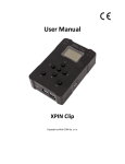
5.2.1
User Manual
Figure 5.3: Keypad
next page
main page
Figure 5.4: LCD Pages
When the power supply is ‘on’, the LCD will display “UNEVERSITI
TEKNOLOGI MALAYSIA” for 3 seconds. It aims to promote the company name
and identify the model of the products. After the 3 seconds, the LCD will display the
main page and ask for password. If you need to activate the cabinet lock, you need to
enter the correct password and press “Enter” button by using the keypad. The
combination length is 6 digits long. When the correct password is entered, the LCD
will display “unlock” that means the lock already activated and you can access the
cabinet now.
67
If the password is wrong, the LCD will display “INVALID CODE” for 1
second, and then you need to enter the password again to activate the cabinet lock.
If the invalid code is entered for 3 times, the LCD will display “WARNING”, the
alarm system will be on. The alarm siren will be ‘on’ and at the same time, a
message will be sending out to inform the authorized person through the mobile
phone. In order to switch off the alarm system, button “ * ” must be pressed and the
LCD will display will main page again. At this time, you need to enter correct
password to switch off the alarm system.
For the password changing, the button “ # ” must be pressed. The LCD will
display next page” Change Password ?”. If you want to change password, the button
“Enter” must be pressed. The system will ask for old password. When the password
is right, you need to enter the new password for 2 times to confirm the new password.
After the password changed successfully, the LCD will display “Password Changed”
for 1 second, the main page will display again.
68
5.3
PCB Layout
5.3.1
Controller Layout (Top Layer)
Figure 5.5: Controller Layout (Top Layer)
69
5.3.2
Controller Circuit (Top Layer)
Figure 5.6: Controller Circuit (Top Layer)
70
5.3.3
Controller Layout (Bottom Layer)
Figure 5-7: Controller Layout (Bottom Layer)
5.3.4
Controller Circuit (Bottom Layer)
Figure 5-8: Controller Circuit (Bottom Layer)
71
5.4
Connector’s Board
This connector’s board has 7 pieces 2-pin header (3 controller header, 2 DC
power supply header, mobile phone header, buzzer header, and motor header).
Figure 5.9: Connector’s Board
From this chapter, the safety cabinet alarm system has been fully explained.
Hence the users can understand the whole development of this alarm system.
CHAPTER 6
CONCLUSION AND FUTURE SUGGESTIONS
6.1
Conclusion
As a conclusion, the project is to come out with the hardware of safety cabinet
alarm system. The safety cabinet alarm system will increase the security cabinet and
make society feel secure to their valuable things. The specifications of the safety cabinet
alarm system are universal LCD alarm system, keyless, flexible, low cost, repairable,
reprogrammable auto reset.
73
6.1
Future Suggestions / Projection
In this project there are plenty of rooms for improvement to further enhance the
project in terms of functionality and reliability. Due to time constraint and lack of
sources, a few suggestions are suggested here for better advancement on the safety
cabinet alarm system in future.
a) Manual Authentication
If black out occurs, the users still can certain manual key to activate the
lock and access the cabinet.
b) Second Authentication
In order to increase security of the cabinet, this system need second
authentication such as fingerprint or image processing to access the cabinet.
c) Improve The Mechanical Part.
The cabinet must be built by certain concrete materials that are not easy to
break in. The cabinet should be fire and water proof to make the safety of
valuable things.
d) Continuous Power Supply
Actually the safety cabinet alarm system need continuous power supply to
operate continually. Rechargeable battery as the backup power supply to
make sure the system is working in 24 hour per day.
The knowledge I acquired from this project from this project will be essential for
me to equip myself for the future electronic industry which is changing rapidly.
74
REFERENCES
[1]
Huang, Han-Way, “PIC microcontroller: an introduction to software and
hardware interfacing”, Clifton Park, NY : Thomson Delmar Learning, 2004
[2]
Iovine, John, “PIC microcontroller project book”, New York : McGraw-Hill,
2000.
[3]
Smith, Jack R, “Programming the PIC microcontroller with MBasic”,
Amsterdam: Elsevier/Newnes, 2005
[4]
Sanchez, Julio, “Microcontroller programming : the microchip PIC”, Boca
Raton, FL : CRC Press, 2007
[5]
Burkhard, Walter A, “C for programmers”, Belmont, Calif: Wadsworth Pub.,
1988
[6]
Weber, Thad L, “Alarm systems and theft prevention”, Boston : Bitterworths
Pub., 1985
[7]
Rakes, Charles D, “Alarms : 55 electronic projects and circuits”, Blue Ridge
Summit, PA : TAB Bks., 1988
[8]
http://us.geocities.com
[9]
http://www.patentstorm.us
[10]
http://www.codelock.us
75
APPENDIX
Source Code
//***********************************************
// Source Code for Safety Cabinet Control System
// Firmware for Microcontroller (PIC 16F876A)
//***********************************************
//Name
: FOO KON SIAN
//IC Number : 840905025205
//Matric No : AE040061
//Course : 4SEE
//Department : INSEED, FKE
//Supervisor : EN Ismail Bin Ariffin
#include <16F876A.h>
#device *=16 ADC=8
//16bit pointer, 8-bit ADC
#use delay(clock=20000000) //20M Hertz
//Initial Configuration Bits
#fuses HS,NOWDT,PROTECT,PUT,NOWRT,BROWNOUT,NOLVP
typedef struct {
int1
int1
int1
int1
int1
int1
int1
int1
} flags;
bit0;
bit1;
bit2;
bit3;
bit4;
bit5;
bit6;
bit7;
//*************************
//Initial value for Port A
//Initial value for Port B
//Initial value for Port C
//*************************
#define TRISA
0b00000000
#define TRISB
0b11111111
#define TRISC
0b10000000
#define Port_Ai
0b00001000
#define Port_Bi
0b00000000
#define Port_Ci
0b00000000
//*************************************
//Label for Port A, Port B, and Port C
//*************************************
//PortA
#define SCLK_H
#define SCLK_L
#define SDIN_H
output_high(PIN_A0)
output_low(PIN_A0)
output_high(PIN_A1)
76
#define SDIN_L output_low(PIN_A1)
#define DC_H output_high(PIN_A2)
#define DC_L output_low(PIN_A2)
#define SEC_H output_high(PIN_A3)
#define SEC_L output_low(PIN_A3)
#define RES_H output_high(PIN_A4)
#define RES_L output_low(PIN_A4)
#define BL_H output_high(PIN_A5)
#define BL_L output_low(PIN_A5)
//Port B
#define KeyIn0 input(PIN_B0)
#define KeyIn1 input(PIN_B1)
#define KeyIn2 input(PIN_B2)
#define KeyIn3 input(PIN_B3)
#define KeyIn4 input(PIN_B4)
#define KeyIn5 input(PIN_B5)
//Port C
#define Scan0_H
output_high(PIN_C0)
#define Scan0_L
output_low(PIN_C0)
#define Scan1_H
output_high(PIN_C1)
#define Scan1_L
output_low(PIN_C1)
#define Scan2_H
output_high(PIN_C2)
#define Scan2_L
output_low(PIN_C2)
#define EN_H
output_high(PIN_C3)
#define EN_L
output_low(PIN_C3)
#define Buzer_L
output_low(PIN_C4)
#define Buzer_H
output_high(PIN_C4)
#define Phone_L
output_low(PIN_C5)
#define Phone_H
output_high(PIN_C5)
#define motor1_L
output_low(PIN_C6)
#define motor1_H
output_high(PIN_C6)
#define motor2_L
output_low(PIN_C7)
#define motor2_H
output_high(PIN_C7)
flags
sys01;
#define flg_10ms
sys01.bit0
//*************************************
//Declare for Integer
//*************************************
int8
int8
int8
int8
int8
int8
int8
int8
int8
int8
int8
int8
int8
int8
tmp;
tmp00 ;
tmp01 ;
tmp02 ;
cnt01 ;
cnt02 ;
cnt03 ;
Dgt_cnt;
bmp_org;
bmp_Bcnt;
tmr10ms;
counter;
change;
keyNew;
77
int8
int8
int8
int8
int8
int8
int8
int8
int8
int8
int8
int8
int8
int8
int8
int8
int8
int8
int8
int8
int8
int8
int8
int8
int8
int8
int8
KeyFlag;
skip;
Skip_2;
SKIP_3;
loop;
keytmp;
keyCnt;
keyNew_2;
keyNew_1;
reset;
shf;
shftmp;
shfct;
cursor;
CsrMarker;
confirm;
code;
try;
DispPg;
bUpdateLCD;
i, k;
W_REG;
page;
FSR;
INDF;
PCLATH;
Temp;
//*************************************
//Constant Data be plced in ROM
//*************************************
//Display Number '1','2','3','4','5','6',7'','8','9','0'
const int8 bmpc[10][7] = {{0, 0x3e, 0x51, 0x49, 0x45, 0x3e, 0},
{0, 0x00, 0x42, 0x7f, 0x40, 0x00, 0},
{0, 0x42, 0x61, 0x51, 0x49, 0x46, 0},
{0, 0x21, 0x41, 0x45, 0x4b, 0x31, 0},
{0, 0x18, 0x14, 0x12, 0x7f, 0x10, 0},
{0, 0x27, 0x45, 0x45, 0x45, 0x39, 0},
{0, 0x3c, 0x4a, 0x49, 0x49, 0x30, 0},
{0, 0x01, 0x71, 0x09, 0x05, 0x03, 0},
{0, 0x36, 0x49, 0x49, 0x49, 0x36, 0},
{0, 0x06, 0x49, 0x49, 0x29, 0x1e, 0}};
//Display "Mark"
const int8 bmpc_2b[7] = {0, 0x7f, 0x7f, 0x7f, 0x7f, 0x7f, 0}; // display all
const int8 bmpc_2c[7] = {0, 0x02, 0x01, 0x51, 0x09, 0x06, 0}; // display '?'
const int8 bmpc_2d[7] = {0, 0x00, 0x60, 0x60, 0x00, 0x00, 0}; // display '.'
const int8 bmpc_2e[7] = {0, 0x08, 0x08, 0x08, 0x08, 0x08, 0}; // display '-'
const int8 bmpc_2f[7] = {0, 0x00, 0x41, 0x22, 0x14, 0x08, 0}; // display '>'
const int8 bmpc_30[7] = {0, 0x08, 0x14, 0x22, 0x41, 0x00, 0}; // display '<'
const int8 bmpc_31[7] = {0x49, 0x2a, 0x1c, 0x7f, 0x1c, 0x2a, 0x49}; // display '*'
const int8 bmpc_32[7] = {0x18, 0x18, 0x18, 0x18, 0x18, 0x18, 0x18}; // display '--'
const int8 bmpc_33[7] = {0x18, 0x18, 0xf8, 0xf8, 0, 0, 0}; // display '-|'
const int8 bmpc_34[7] = {0, 0, 0xf8, 0xf8, 0x18, 0x18, 0x18}; // display '|-'
const int8 bmpc_35[7] = {0, 0, 0x1f, 0x1f, 0x18, 0x18, 0x18}; // display '|_'
78
const int8 bmpc_36[7] = {0x18, 0x18, 0x1f, 0x1f, 0, 0, 0}; // display '_|'
const int8 bmpc_37[7] = {0, 0, 0xff, 0xff, 0, 0, 0}; // display '|'
const int8 bmpc_40h[7] = {0, 0, 0, 0, 0, 0, 0};//dislay'blank'
//Display Character from 'A' to 'Z'
const int8 bmpc_AAMM[13][7] = { {0, 0x7e, 0x11, 0x11, 0x11, 0x7e, 0}, //A...M
{0, 0x7f, 0x49, 0x49, 0x49, 0x36, 0},
{0, 0x3e, 0x41, 0x41, 0x41, 0x22, 0},
{0, 0x7f, 0x41, 0x41, 0x22, 0x1c, 0},
{0, 0x7f, 0x49, 0x49, 0x49, 0x41, 0},
{0, 0x7f, 0x09, 0x09, 0x09, 0x01, 0},
{0, 0x3e, 0x41, 0x49, 0x49, 0x7a, 0},
{0, 0x7f, 0x08, 0x08, 0x08, 0x7f, 0},
{0, 0x00, 0x41, 0x7f, 0x41, 0x00, 0},
{0, 0x20, 0x40, 0x41, 0x3f, 0x01, 0},
{0, 0x7f, 0x08, 0x14, 0x22, 0x41, 0},
{0, 0x7f, 0x40, 0x40, 0x40, 0x40, 0},
{0, 0x7f, 0x02, 0x0c, 0x02, 0x7f, 0}};
const int8 bmpc_NNZZ[13][7] = { {0, 0x7f, 0x04, 0x08, 0x10, 0x7f, 0}, //N...Z
{0, 0x3e, 0x41, 0x41, 0x41, 0x3e, 0},
{0, 0x7f, 0x09, 0x09, 0x09, 0x06, 0},
{0, 0x3e, 0x41, 0x51, 0x21, 0x5e, 0},
{0, 0x7f, 0x09, 0x19, 0x29, 0x46, 0},
{0, 0x46, 0x49, 0x49, 0x49, 0x31, 0},
{0, 0x01, 0x01, 0x7f, 0x01, 0x01, 0},
{0, 0x3f, 0x40, 0x40, 0x40, 0x3f, 0},
{0, 0x1f, 0x20, 0x40, 0x20, 0x1f, 0},
{0, 0x3f, 0x40, 0x38, 0x40, 0x3f, 0},
{0, 0x63, 0x14, 0x08, 0x14, 0x63, 0},
{0, 0x07, 0x08, 0x70, 0x08, 0x07, 0},
{0, 0x61, 0x51, 0x49, 0x45, 0x43, 0}};
//Display Character from 'a' to 'z'
const int8 bmpc_am[13][7] = {{0, 0x20, 0x54, 0x54, 0x54, 0x78, 0}, //a...m
{0, 0x7f, 0x48, 0x44, 0x44, 0x38, 0},
{0, 0x38, 0x44, 0x44, 0x44, 0x20, 0},
{0, 0x38, 0x44, 0x44, 0x48, 0x7f, 0},
{0, 0x38, 0x54, 0x54, 0x54, 0x18, 0},
{0, 0x08, 0x7e, 0x09, 0x01, 0x02, 0},
{0, 0x0c, 0x52, 0x52, 0x52, 0x3e, 0},
{0, 0x7e, 0x08, 0x04, 0x04, 0x78, 0},
{0, 0x00, 0x44, 0x7d, 0x40, 0x00, 0},
{0, 0x20, 0x40, 0x44, 0x3d, 0x00, 0},
{0, 0x7f, 0x10, 0x28, 0x44, 0x00, 0},
{0, 0x00, 0x41, 0x7f, 0x40, 0x00, 0},
{0, 0x7c, 0x04, 0x18, 0x04, 0x78, 0}};
const int8 bmpc_nz[13][7] = { {0, 0x7c, 0x08, 0x04, 0x04, 0x78, 0},
{0, 0x38, 0x44, 0x44, 0x44, 0x38, 0},
{0, 0x7c, 0x14, 0x14, 0x14, 0x08, 0},
{0, 0x08, 0x14, 0x14, 0x18, 0x7c, 0},
{0, 0x7c, 0x08, 0x04, 0x04, 0x08, 0},
{0, 0x48, 0x54, 0x54, 0x54, 0x20, 0},
79
{0, 0x04, 0x3f, 0x44, 0x40, 0x20, 0},
{0, 0x3c, 0x40, 0x40, 0x20, 0x7c, 0},
{0, 0x1c, 0x20, 0x40, 0x20, 0x1c, 0},
{0, 0x3c, 0x40, 0x30, 0x40, 0x3c, 0},
{0, 0x44, 0x28, 0x10, 0x28, 0x44, 0},
{0, 0x0c, 0x50, 0x50, 0x50, 0x3c, 0},
{0, 0x44, 0x64, 0x54, 0x4c, 0x44, 0}};
//display "UNIVERSITI"
const char con_sole1[12] = {'U', 'N', 'I', 'V', 'E', 'R', 'S', 'I', 'T', 'I', 0xa2, 0xa2};
//display "TEKNOLOGI"
const char con_sole2[12] = {'T', 'E', 'K', 'N', 'O', 'L', 'O', 'G', 'I', 0xa2, 0xa2, 0xa2};
//display "MALAYSIA"
const char con_sole3[12] = {'M', 'A', 'L', 'A', 'Y', 'S', 'I', 'A', 0xa2, 0xa2, 0xa2, 0xa2};
#define rd
#define sentRd
RdFlg.bit0
RdFlg.bit4
//**************************************************************
// RAM variables (Array)
//**************************************************************
int8 LCDRow0[12];
int8 LCDRow1[12];
int8 LCDRow2[12];
int8 LCDRow3[12];
int8 LCDRow4[12];
int8 LCDRow5[12];
int8 digit[6];
int8 second[6];
int8 save[6];
//**************************************************************
// LCD Display Program
//**************************************************************
void dly0()
{
cnt01 = W_REG;
dly01:
cnt02 = 0x1f;
dly02:
cnt03 = 0xff;
dly03:
cnt03--;
if (cnt03 != 0) goto dly03;
dly04:
cnt02--;
if (cnt02 != 0) goto dly02;
dly05:
cnt01--;
if (cnt01 != 0) goto dly01;
}
80
void dly1()
{
W_REG = 8;
dly0();
}
void dly2()
{
W_REG = 2;
dly0();
}
void dly3()
{
W_REG = 1;
dly0();
}
void shf8()
{
W_REG = 8;
shfct = W_REG;
Shf8a:
SCLK_L;
Temp = shf;
rotate_left(&shf,1);
if(Temp < 0x80)
{
goto
shfb0;
}
SDIN_H; //bit 1
goto shfclk;
shfb0:
SDIN_L; //bit 0
shfclk:
SCLK_H;
ckshfct:
shfct--;
if(shfct != 0)
{
goto shf8a;
}
shf8b:
SCLK_L;
SDIN_L;
}
void ShfCmd()
{
shf = W_REG;
DC_L;
81
shf8();
}
//shift
void shfdata()
{
shf = W_REG;
DC_H;
shf8();
}
void sdly1()
{
//nop
return;
}
//row data
void d_row()
{
shftmp = W_REG; //row data
cnt03 = 0x54;
d_row2:
W_REG = shftmp; //row data
ShfData();
cnt03--;
if(cnt03 != 0)
{
goto d_row2;
}
}
void Init_LCD_row() //cmd
{
W_REG = (W_REG + 0b01000000);
SEC_L; //enable clk
ShfCmd();
W_REG = 0b10000000;
ShfCmd();
SEC_H; //disable clk
SEC_L; //disable clk
W_REG = 0b10101100; //initial data
//
W_REG = 0; //initial data
d_row();
SEC_H; //disable clk
}
//Init LCD
void Init_LCD()
{
82
//Init LCD starts here
dly2();
SEC_H; //disable clk
DC_H;
sdly1();
RES_H; //release reset
dly3();
go00:
SEC_L; // enable clk
W_REG = 0b00100100;
ShfCmd();
for(i=0; i<6; i++)
{
W_REG = i;
Init_LCD_row();
}
SEC_L; //enable clk
W_REG = 0b00100000;
ShfCmd();
SEC_H; //disable clk
dly1();
dly1();
SEC_L; //enable clk
W_REG = 0b00100000;
ShfCmd();
W_REG = 0b00001100;
ShfCmd();
SEC_H; //disable clk
dly1();
dly1();
}
//Update 1 digit LCD Data
void LCD_dgt()
{
Nxt_CHAR_B:
bmp_org++;
if(--bmp_Bcnt != 0) goto Nxt_CHAR_B;
return;
LCD_dgt_num:
W_REG = 0x08;
PCLATH = W_REG;
bmp_Bcnt = 0x07;
Nxt_num_B:
W_REG = bmp_org;
W_REG = W_REG + CsrMarker;
ShfData();
bmp_org++;
if (--bmp_Bcnt != 0)
83
{
goto Nxt_num_B;
}
return;
Chk_cursor_pos:
return;
}
//Update 1 row
void Udp_row()
{
W_REG = W_REG + 0x40;
SEC_L; //enable clk
ShfCmd();
W_REG = 0x80;
ShfCmd();
SEC_H; //disable clk
W_REG = 0x0c; //dgt count
Dgt_cnt = W_REG;
SEC_L; //enable clk
Nxt_dgt:
CsrMarker = 0;
if (DispPg != 0) goto Nxt_dgt0;
if (cursor == FSR)
{
CsrMarker = 0x80;
}
Nxt_dgt0:
#asm
movf INDF,W
#endasm
LCD_dgt();
#asm
incf FSR,F
#endasm
}
//LCD Display Program
void Udp_LCD()
{
Udp_row();
}
void Udp_LCD0()
{
Udp_LCD();
}
84
//*************************************
// To Interupt Every 10 ms
//*************************************
#INT_TIMER1
void IRQ_T1()
{
set_timer1(0xe796);
//10ms (0xe796)
enable_interrupts(INT_TIMER1);
flg_10ms = 1;
}
//*************************************
// Functions for LCD Display
//*************************************
void display_blank()
{
for (i=0; i<7; i++) {
W_REG = bmpc_40h[i];
shfdata();
}
}
void display_AAMM(int8 x)
{
for (i=0; i<7; i++) {
W_REG = bmpc_AAMM[x][i];
shfdata();
}
}
void display_NNZZ(int8 x)
{
for (i=0; i<7; i++) {
W_REG = bmpc_NNZZ[x][i];
shfdata();
}
}
void display_am(int8 x)
{
for (i=0; i<7; i++) {
W_REG = bmpc_am[x][i];
shfdata();
}
}
void display_nz(int8 x)
{
for (i=0; i<7; i++) {
W_REG = bmpc_nz[x][i];
shfdata();
}
}
85
void display(int8 x)
{
for (i=0; i<7; i++) {
W_REG = bmpc[x][i];
shfdata();
}
}
void display_cursor()
{
for (i=0; i<7; i++) {
W_REG = bmpc_40h[i] | 0x80;
shfdata();
}
}
void display_all()
{
for (i=0; i<7; i++) {
W_REG = bmpc_2b[i];
shfdata();
}
}
void display_question()
{
for (i=0; i<7; i++) {
W_REG = bmpc_2c[i];
shfdata();
}
}
void display_dot()
{
for (i=0; i<7; i++) {
W_REG = bmpc_2d[i];
shfdata();
}
}
void display_minus()
{
for (i=0; i<7; i++) {
W_REG = bmpc_2e[i];
shfdata();
}
}
void display_greater()
{
for (i=0; i<7; i++) {
W_REG = bmpc_2f[i];
86
shfdata();
}
}
void display_lower()
{
for (i=0; i<7; i++) {
W_REG = bmpc_30[i];
shfdata();
}
}
void display_line()
{
for (i=0; i<7; i++) {
W_REG = bmpc_32[i];
shfdata();
}
}
void display_vertical()
{
for (i=0; i<7; i++) {
W_REG = bmpc_37[i];
shfdata();
}
}
void display_box45()
{
for (i=0; i<7; i++) {
W_REG = bmpc_33[i];
shfdata();
}
}
void display_box135()
{
for (i=0; i<7; i++) {
W_REG = bmpc_34[i];
shfdata();
}
}
void display_box225()
{
for (i=0; i<7; i++) {
W_REG = bmpc_35[i];
shfdata();
87
}
}
void display_box315()
{
for (i=0; i<7; i++) {
W_REG = bmpc_36[i];
shfdata();
}
}
void display_star()
{
for (i=0; i<7; i++) {
W_REG = bmpc_31[i];
shfdata();
}
}
void show_char()
{
if (W_REG == 0xa2) {
display_blank();
return; }
if ((W_REG >= 0x41) && (W_REG <= 0x4D)) {
W_REG -= 0x41;
display_AAMM(W_REG);
return;
}
//A...M
if ((W_REG >= 0x4E) && (W_REG <= 0x5A)) {
W_REG -= 0x4E;
display_NNZZ(W_REG);
return;
}
//N...Z
if ((W_REG >= 0x61) && (W_REG <= 0x6d)) {
W_REG -= 0x61;
display_am(W_REG);
return;
}
//a...m
if ((W_REG >= 0x6e) && (W_REG <= 0x7a)) {
W_REG -= 0x6e;
display_nz(W_REG);
return;
}
//n...z
if ((W_REG >= 0x30) && (W_REG <= 0x39)) {
W_REG -= 0x30;
//0..9
88
display(W_REG);
return;
}
if (W_REG == 0x3f) {
display_question();
return; }
if (W_REG == 0x2e) {
display_dot();
return; }
if (W_REG == 0x2d) {
display_minus();
return; }
if (W_REG == 0x3e) {
display_greater();
return; }
if (W_REG == 0x3c) {
display_lower();
return; }
if (W_REG == 0x2a) {
display_star();
return; }
if (W_REG == 0x11) {
display_box45();
return; }
if (W_REG == 0x12) {
display_box135();
return; }
if (W_REG == 0x13) {
display_box225();
return; }
if (W_REG == 0x14) {
display_box315();
return; }
if (W_REG == 0x15) {
display_line();
return; }
if (W_REG == 0x16) {
display_vertical();
return; }
}
89
void display_char()
{
for(k=0; k<12; k++){
W_REG = LCDRow0[k];
show_char();
}
for(k=0; k<12; k++){
W_REG = LCDRow1[k];
show_char();
}
for(k=0; k<12; k++){
W_REG = LCDRow2[k];
show_char();
}
for(k=0; k<12; k++){
W_REG = LCDRow3[k];
show_char();
}
for(k=0; k<12; k++){
W_REG = LCDRow4[k];
show_char();
}
for(k=0; k<12; k++){
W_REG = LCDRow5[k];
show_char();
}
}
void clear()
{
for(i=0; i<12; i++){
LCDRow2[i] = 0xa2;
LCDRow3[i] = 0xa2;
LCDRow4[i] = 0xa2;
LCDRow5[i] = 0xa2;
}
}
void upper_box()
{
LCDRow1[0] = 0xa2;
LCDRow1[1] = 0x12;
for(i=2; i<10; i++){
LCDRow1[i] = 0x15;
}
LCDRow1[10] = 0x11;
LCDRow1[11] = 0xa2;
clear();
LCDRow2[0] = 0xa2;
90
LCDRow2[1] = 0x16;
for(i=2; i<10; i++){
LCDRow2[i] = 0xa2;
}
LCDRow2[10] = 0x16;
LCDRow2[11] = 0xa2;
LCDRow3[0] = 0xa2;
LCDRow3[1] = 0x13;
for(i=2; i<10; i++){
LCDRow3[i] = 0x15;
}
LCDRow3[10] = 0x14;
LCDRow3[11] = 0xa2;
for(i=0; i<12; i++){
LCDRow4[i] = 0xa2;
LCDRow5[i] = 0xa2;
}
}
//*************************************
// Pages In LCD display
//*************************************
void page_0()
{
for(i=0; i<12; i++){
LCDRow0[i] = con_sole1[i];
LCDRow1[i] = con_sole2[i];
LCDRow2[i] = con_sole3[i];
}
for(i=0; i<12; i++){
LCDRow3[i] = 0xa2;
LCDRow4[i] = 0xa2;
LCDRow5[i] = 0xa2;
}
}
void page_1()
//Password ?
{
LCDRow0[0] = 'P';
LCDRow0[1] = 'a';
LCDRow0[2] = 's';
LCDRow0[3] = 's';
LCDRow0[4] = 'w';
LCDRow0[5] = 'o';
LCDRow0[6] = 'r';
LCDRow0[7] = 'd';
LCDRow0[8] = 0xa2;
91
LCDRow0[9] = 0x3f; //'?'
LCDRow0[10] = 0xa2;
LCDRow0[11] = 0xa2;
upper_box();
}
void page_2()
//Change password ?
{
LCDRow0[0] = 'C';
LCDRow0[1] = 'h';
LCDRow0[2] = 'a';
LCDRow0[3] = 'n';
LCDRow0[4] = 'g';
LCDRow0[5] = 'e';
for(i=6; i<12; i++) {
LCDRow0[i] = 0xa2;
}
LCDRow1[0] = 'P';
LCDRow1[1] = 'a';
LCDRow1[2] = 's';
LCDRow1[3] = 's';
LCDRow1[4] = 'w';
LCDRow1[5] = 'o';
LCDRow1[6] = 'r';
LCDRow1[7] = 'd';
LCDRow1[8] = 0xa2;
LCDRow1[9] = 0x3f; //'?'
LCDRow1[10] = 0xa2;
LCDRow1[11] = 0xa2;
clear();
}
void password()
{
LCDRow1[0] = 'P';
LCDRow1[1] = 'a';
LCDRow1[2] = 's';
LCDRow1[3] = 's';
LCDRow1[4] = 'w';
LCDRow1[5] = 'o';
LCDRow1[6] = 'r';
LCDRow1[7] = 'd';
LCDRow1[8] = 0xa2;
LCDRow1[9] = 0x3f; //'?'
LCDRow1[10] = 0xa2;
LCDRow1[11] = 0xa2;
LCDRow2[0] = 0xa2;
LCDRow2[1] = 0x12;
for(i=2; i<10; i++){
LCDRow2[i] = 0x15;
}
LCDRow2[10] = 0x11;
92
LCDRow2[11] = 0xa2;
LCDRow3[0] = 0xa2;
LCDRow3[1] = 0x16;
for(i=2; i<10; i++){
LCDRow3[i] = 0xa2;
}
LCDRow3[10] = 0x16;
LCDRow3[11] = 0xa2;
LCDRow4[0] = 0xa2;
LCDRow4[1] = 0x13;
for(i=2; i<10; i++){
LCDRow4[i] = 0x15;
}
LCDRow4[10] = 0x14;
LCDRow4[11] = 0xa2;
for(i=0; i<12; i++){
LCDRow5[i] = 0xa2;
}
}
void page_3()
//Old Password ?
{
LCDRow0[0] = 'O';
LCDRow0[1] = 'l';
LCDRow0[2] = 'd';
for(i=3; i<12; i++){
LCDRow0[i] = 0xa2;
}
password();
}
void page_4()
//New Password ?
{
try = 0;
LCDRow0[0] = 'N';
LCDRow0[1] = 'e';
LCDRow0[2] = 'w';
for(i=3; i<12; i++){
LCDRow0[i] = 0xa2;
}
password();
}
void page_9()
{
//Confirm ?
93
LCDRow0[0] = 'C';
LCDRow0[1] = 'o';
LCDRow0[2] = 'n';
LCDRow0[3] = 'f';
LCDRow0[4] = 'i';
LCDRow0[5] = 'r';
LCDRow0[6] = 'm';
LCDRow0[7] = 0xa2;
LCDRow0[8] = 0x3f; //'?'
LCDRow0[9] = 0xa2;
LCDRow0[10] = 0xa2;
LCDRow0[11] = 0xa2;
upper_box();
}
void page_5()
//Password Changed
{
try = 0;
code = 0;
LCDRow0[0] = 'P';
LCDRow0[1] = 'a';
LCDRow0[2] = 's';
LCDRow0[3] = 's';
LCDRow0[4] = 'w';
LCDRow0[5] = 'o';
LCDRow0[6] = 'r';
LCDRow0[7] = 'd';
LCDRow0[8] = 0xa2;
LCDRow0[9] = 0xa2;
LCDRow0[10] = 0xa2;
LCDRow0[11] = 0xa2;
LCDRow1[0] = 'C';
LCDRow1[1] = 'h';
LCDRow1[2] = 'a';
LCDRow1[3] = 'n';
LCDRow1[4] = 'g';
LCDRow1[5] = 'e';
LCDRow1[6] = 'd';
for(i=7; i<12; i++){
LCDRow1[i] = 0xa2;
}
clear();
}
void page_6()
//Invalid Code
{
try++;
counter = 0;
for(i=0; i<12; i++){
LCDRow0[i] = 0xa2;
94
LCDRow1[i] = 0xa2;
LCDRow3[i] = 0xa2;
LCDRow4[i] = 0xa2;
LCDRow5[i] = 0xa2;
}
LCDRow2[0] = 'I';
LCDRow2[1] = 'n';
LCDRow2[2] = 'v';
LCDRow2[3] = 'a';
LCDRow2[4] = 'l';
LCDRow2[5] = 'i';
LCDRow2[6] = 'd';
LCDRow2[7] = 0xa2;
LCDRow2[8] = 'C';
LCDRow2[9] = 'o';
LCDRow2[10] = 'd';
LCDRow2[11] = 'e';
}
void page_7()
{
//Warning !
for(i=0; i<12; i++){
LCDRow0[i] = 0xa2;
LCDRow1[i] = 0xa2;
LCDRow3[i] = 0xa2;
LCDRow4[i] = 0xa2;
LCDRow5[i] = 0xa2;
}
LCDRow2[0] = 0xa2;
LCDRow2[1] = 0xa2;
LCDRow2[2] = 'W';
LCDRow2[3] = 'a';
LCDRow2[4] = 'r';
LCDRow2[5] = 'n';
LCDRow2[6] = 'i';
LCDRow2[7] = 'n';
LCDRow2[8] = 'g';
LCDRow2[9] = 0xa2;
LCDRow2[10] = 0xa2;
LCDRow2[11] = 0xa2;
}
void page_8()
//Unlock !
{
try = 0;
code = 0;
for(i=0; i<12; i++){
LCDRow0[i] = 0xa2;
95
LCDRow1[i] = 0xa2;
LCDRow3[i] = 0xa2;
LCDRow4[i] = 0xa2;
LCDRow5[i] = 0xa2;
}
LCDRow2[0] = 0xa2;
LCDRow2[1] = 0xa2;
LCDRow2[2] = 'U';
LCDRow2[3] = 'n';
LCDRow2[4] = 'l';
LCDRow2[5] = 'o';
LCDRow2[6] = 'c';
LCDRow2[7] = 'k';
LCDRow2[8] = 0xa2;
LCDRow2[9] = 0xa2;
LCDRow2[10] = 0xa2;
LCDRow2[11] = 0xa2;
}
void pages()
{
if(page == 1) page_1();
if(page == 2) page_2();
if(page == 3) page_3();
if(page == 4) page_4();
if(page == 9) page_9();
}
//*************************************
// Count Numbers of Entered Digit
//*************************************
void counter_1()
{
if(change == 0){
switch(counter){
case 0: digit[0] = tmp;
counter++;
break;
case 1: digit[1] = tmp;
counter++;
break;
case 2: digit[2] = tmp;
counter++;
break;
case 3: digit[3] = tmp;
counter++;
break;
case 4: digit[4] = tmp;
counter++;
break;
case 5: digit[5] = tmp;
96
counter++;
break;
case 6: counter++;
}
}
if(change == 1){
switch(counter){
case 0: second[0] = tmp;
counter++;
break;
case 1: second[1] = tmp;
counter++;
break;
case 2: second[2] = tmp;
counter++;
break;
case 3: second[3] = tmp;
counter++;
break;
case 4: second[4] = tmp;
counter++;
break;
case 5: second[5] = tmp;
counter++;
break;
case 6: counter++;
change = 0;
}
}
}
//*************************************
// Display 'Star' for each entered code
//*************************************
void set_star_1() //In page_1
{
switch(counter){
case 0: LCDROW2[3] = 0X2a;
break;
case 1: LCDROW2[4] = 0X2a;
break;
case 2: LCDROW2[5] = 0X2a;
break;
case 3: LCDROW2[6] = 0X2a;
break;
case 4: LCDROW2[7] = 0X2a;
break;
case 5: LCDROW2[8] = 0X2a;
break;
}
}
void set_star_2() //In page_3
{
switch(counter){
97
case 0: LCDROW3[3] = 0X2a;
break;
case 1: LCDROW3[4] = 0X2a;
break;
case 2: LCDROW3[5] = 0X2a;
break;
case 3: LCDROW3[6] = 0X2a;
break;
case 4: LCDROW3[7] = 0X2a;
break;
case 5: LCDROW3[8] = 0X2a;
break;
}
}
//*******************************************
// Make Sure Only 6 Digits for Any Password
//*******************************************
void check_counter()
{
if(counter >= 7 ){
page_6();
SEC_L;
display_char();
SEC_H;
delay_ms(1000);
if(page == 1)page_1();
if(page == 3)page_3();
if(page == 4 || page == 9)page_4();
counter = 0;
}
}
//***************************
// Save Digits For Password
//***************************
void save_digit()
{
save[0] = 0x32;
save[1] = 0x33;
save[2] = 0x34;
save[3] = 0x35;
save[4] = 0x36;
save[5] = 0x37;
}
//*****************
// Check Password
//*****************
void check_password()
{
code = 0;
98
read_program_memory(0x1800, save, 6);
if(save[0] == 0xff){save_digit();}
if(digit[0] == save[0]) code++;
if(digit[1] == save[1]) code++;
if(digit[2] == save[2]) code++;
if(digit[3] == save[3]) code++;
if(digit[4] == save[4]) code++;
if(digit[5] == save[5]) code++;
digit[0] = 88;
}
void check_new_password()
{
confirm = 0;
if(digit[0] == second[0]) confirm++;
if(digit[1] == second[1]) confirm++;
if(digit[2] == second[2]) confirm++;
if(digit[3] == second[3]) confirm++;
if(digit[4] == second[4]) confirm++;
if(digit[5] == second[5]) confirm++;
}
//*****************
// Change Password
//*****************
void change_password()
{
save[0] = digit[0];
save[1] = digit[1];
save[2] = digit[2];
save[3] = digit[3];
save[4] = digit[4];
save[5] = digit[5];
write_program_memory(0x1800, save, 6);
}
//*******************************************
// Identify The Pressed Button at Keypad
//*******************************************
void press_1()
{
tmp = 0x31;
counter_1();
check_counter();
}
void press_2()
{
tmp = 0x32;
counter_1();
check_counter();
}
99
void press_3()
{
tmp = 0x33;
counter_1();
check_counter();
}
void press_4()
{
tmp = 0x34;
counter_1();
check_counter();
}
void press_5()
{
tmp = 0x35;
counter_1();
check_counter();
}
void press_6()
{
tmp = 0x36;
counter_1();
check_counter();
}
void press_7()
{
tmp = 0x37;
counter_1();
check_counter();
}
void press_8()
{
tmp = 0x38;
counter_1();
check_counter();
}
void press_9()
{
tmp = 0x39;
counter_1();
check_counter();
}
void press_0()
{
tmp = 0x30;
counter_1();
check_counter();
}
100
void confirm_page_next()
{
page = 2;
pages();
}
void confirm_page_back()
{
page = 1;
pages();
}
void keytest()
{
int8 x;
for (x=0; x<6; x++) {
if ( bit_test(keytmp, 0) == 0) {
keyNew = keyCnt;
skip_2 = 1;
KeyFlag = 1;
}
shift_right(&keytmp,1,1);
keyCnt++;
}
}
void identify_key()
{
KeyFlag = 0;
keycnt = 0;
keytmp = tmp00;
keytest();
if(KeyFlag == 0) {
keytmp = tmp01;
keytest();
}
if(KeyFlag == 0) {
keytmp = tmp02;
keytest();
}
}
void confirm_key()
{
if(keyNew == 6) {
bUpdateLCD = 1;
if (page == 1) {set_star_1();
press_1();
}
if (page == 3) { set_star_2();
press_1();
}
if (page == 4 || page == 9) {
101
if(page == 4) set_star_2();
if(page == 9) set_star_1();
press_1();
}
}
if(keyNew == 7) {
bUpdateLCD = 1;
if (page == 1) { set_star_1();
press_2();
}
if (page == 3) { set_star_2();
press_2();
}
if (page == 4 || page == 9) {
if(page == 4) set_star_2();
if(page == 9) set_star_1();
press_2();
}
}
if(keyNew == 8) {
bUpdateLCD = 1;
if (page == 1) {
set_star_1();
press_3();
}
if (page == 3) { set_star_2();
press_3();
}
if (page == 4 || page == 9) {
if(page == 4) set_star_2();
if(page == 9) set_star_1();
press_3();
}
}
if(keyNew == 9) {
bUpdateLCD = 1;
if (page == 1) { set_star_1();
press_4();
}
if (page == 3) { set_star_2();
press_4();
}
if (page == 4 || page == 9) {
if(page == 4) set_star_2();
if(page == 9) set_star_1();
press_4();
}
}
if(keyNew == 10) {
bUpdateLCD = 1;
if (page == 1) {set_star_1();
press_5();
if (page == 3) { set_star_2();
}
102
press_5();
}
if (page == 4 || page == 9) {
if(page == 4) set_star_2();
if(page == 9) set_star_1();
press_5();
}
}
if(keyNew == 11) {bUpdateLCD = 1;
if (page == 1) { set_star_1();
press_6();
}
if (page == 3) { set_star_2();
press_6();
}
if (page == 4 || page == 9) {
if(page == 4) set_star_2();
if(page == 9) set_star_1();
press_6();
}
}
if(keyNew == 12) {bUpdateLCD = 1;
if (page == 1) {set_star_1();
press_7();
}
if (page == 3) { set_star_2();
press_7();
}
if (page == 4 || page == 9) {
if(page == 4) set_star_2();
if(page == 9) set_star_1();
press_7();
}
}
if(keyNew == 13) {bUpdateLCD = 1;
if (page == 1) { set_star_1();
press_8();
}
if (page == 3) { set_star_2();
press_8();
}
if (page == 4 || page == 9) {
if(page == 4) set_star_2();
if(page == 9) set_star_1();
press_8();
}
}
if(keyNew == 14) {bUpdateLCD = 1;
if (page == 1) {
set_star_1();
103
press_9();
}
if (page == 3) { set_star_2();
press_9();
}
if (page == 4 || page == 9) {
if(page == 4) set_star_2();
if(page == 9) set_star_1();
press_9();
}
}
if(keyNew == 16) {bUpdateLCD = 1;
if (page == 1) {set_star_1();
press_0();
}
if (page == 3) { set_star_2();
press_0();
}
if (page == 4 || page == 9) {
if(page == 4) set_star_2();
if(page == 9) set_star_1();
press_0();
}
}
}
void confirm_key2()
{
if(keyNew == 1) {bUpdateLCD = 1;//enter
if (page == 1) {
check_password();
if(code == 6) { page_8();
Buzer_L;
motor1_H;
motor2_L;
EN_H;
delay_ms(12);
EN_L;}
else {page_6();
SEC_L;
display_char();
SEC_H;
delay_ms(1000);
pages();}
}
if (page == 9) {
change = 0;
if(counter == 6){
counter = 0;
check_new_password();
if(confirm == 6) {
change_password();
104
else {
page_5();
SEC_L;
display_char();
SEC_H;
delay_ms(1000);
page = 1;
pages();
}
page_6();
SEC_L;
display_char();
SEC_H;
delay_ms(1000);
page = 4;
pages();
return;
}
}
else {
page_6();
SEC_L;
display_char();
SEC_H;
delay_ms(1000);
page = 4;
pages();
return;
}
}
if (page == 4) {if(counter == 6) {
page = 9;
pages();
change = 1;
}
else {
page_6();
SEC_L;
display_char();
SEC_H;
delay_ms(1000);
page_4();
}
}
if (page == 3) {
check_password();
if(code == 6) {page = 4;
pages();
}
else {
page_6();
SEC_L;
display_char();
SEC_H;
delay_ms(1000);
pages();
105
}
}
if (page == 2) {page = 3;
pages();
return;}
counter = 0;
}
if(keyNew == 2) { //press down
bUpdateLCD = 1;
counter = 0;
confirm_page_back();
motor1_L;
motor2_H;
EN_H;
delay_ms(12);
EN_L;
}
if(keyNew == 5) { //press up
bUpdateLCD = 1;
Phone_H;
delay_ms(1000);
Phone_L;
}
if(keyNew == 15){ //
bUpdateLCD = 1;
counter = 0;
confirm_page_back();
}
if(keyNew == 17) {
//press next
bUpdateLCD = 1;
counter = 0;
confirm_page_next();
}
}
//**************
// Scan for key
//**************
void scan_key()
{
Scan0_L;
delay_us(10);
tmp00 = input_b()| 0xC0;
Scan0_H;
Scan1_L;
delay_us(10);
tmp01 = input_b()| 0xC0;
106
Scan1_H;
Scan2_L;
delay_us(10);
tmp02 = input_b()| 0xC0;
Scan2_H;
}
//****************************
// Activate Alarm System
//****************************
void security()
{
if(try == 3) {
page_7();
SEC_L;
display_char();
SEC_H;
Phone_H;
delay_ms(1000);
Phone_L;
Buzer_H;
try = 0;
}
}
//*******************
// Initiation System
//*******************
void Init()
{
port_b_pullups(TRUE);
output_a(PORT_Ai);
output_b(PORT_Bi);
output_c(PORT_Ci);
set_tris_a(TRISA);
set_tris_b(TRISB);
set_tris_c(TRISC);
Init_LCD();
SEC_L;
page_0();
SEC_L;
display_char();
SEC_H;
Phone_L;
Buzer_L;
EN_L;
BL_H;
delay_ms(3000);
page_1();
SEC_L;
display_char();
SEC_H;
Scan0_H;
Scan1_H;
107
Scan2_H;
save_digit();
page = 1;
counter = 0;
code = 0;
change = 0;
try = 0;
setup_timer_1(T1_INTERNAL | T1_DIV_BY_8);
set_timer1(0xe796);
//10ms
enable_interrupts(INT_RDA);
enable_interrupts(GLOBAL);
enable_interrupts(INT_TIMER1);
}
void main()
{
Init();
mainloop:
do {
} while (!flg_10ms);
flg_10ms = 0;
if (skip_3 == 0){ scan_key();
identify_key();
}
if (loop == 0) keyNew_1 = keyNew;
if (loop == 1) { keyNew_2 = keyNew;
reset = 1;
}
loop++;
if (reset == 1) {
loop = 0;
reset = 0;
}
if (skip_2 == 1){
skip_2 = 0;
if(keyNew_1 == keyNew_2) skip = 1;
}
if (skip == 1){
confirm_key();
confirm_key2();
keyNew_1 = 21;
keyNew_2 = 22;
skip = 0;
skip_3 = 1;
}
tmr10ms++;
if(tmr10ms <= 9) goto mainloop;
security();
tmr10ms = 0;
skip = 0;
skip_3 = 0;
loop = 0;
keyCnt = 0;
108
keyNew = 20;
keyNew_1 = 21;
keyNew_2 = 22;
if (bUpdateLCD) {
SEC_L;
display_char();
SEC_H;
bUpdateLCD = 0;
}
check_key:
scan_key();
if (tmp00 == 0xff){
if (tmp01 == 0xff){
if(tmp02 == 0xff) { goto mainloop;}
}
}
goto check_key;
}