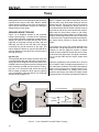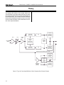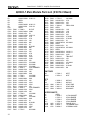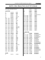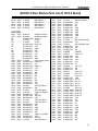
1
Power Base-1 & 460CSL Amplifier Service Manual
POWER AMPLIFIER
SERVICE MANUAL
POWER BASE-1 & 460CSL
®
™
©1995 by CROWN INTERNATIONAL, INC.
Mailing Address:
P.O. Box 1000
Elkhart, IN U.S.A. 46515-1000
Shipping Address:
57620 C.R. 105
Elkhart, IN U.S.A. 46517
CSL™ is a trademark and Power Base-1,® ODEP ® and Crown® are registered trademarks of Crown International, Inc.
K-SVCPB1
1-95
1
Power Base-1 & 460CSL Amplifier Service Manual
The information furnished in this manual does not include all of the details of design, production, or variations
of the equipment. Nor does it cover every possible situation which may arise during installation, operation or
maintenance. If you need special assistance beyond the scope of this manual, please contact the Crown
Technical Support Group.
Mail: P.O. Box 1000 Elkhart IN 46515-1000
Shipping: 57620 C.R. 105 Elkhart IN 46517
Phone: (800) 342-6939/(219) 294-8200
FAX: (219) 294-8301
CAUTION
AVIS
TO PREVENT ELECTRIC SHOCK DO
NOT REMOVE TOP OR BOTTOM
COVERS. NO USER SERVICEABLE
PARTS INSIDE. REFER SERVICING
TO QUALIFIED SERVICE
PERSONNEL. DISCONNECT
POWER CORD BEFORE REMOVING
REAR INPUT MODULE TO ACCESS
GAIN SWITCH.
À PRÉVENIR LE CHOC
ÉLECTRIQUE N’ENLEVEZ
PAS LES COUVERTURES.
RIEN DES PARTIES
UTILES À L’INTÉRIEUR.
DÉBRANCHER LA BORNE
AVANT D’OUVRIR LA
MODULE EN ARRIÈRE.
WARNING
TO REDUCE THE RISK OF ELECTRIC
SHOCK, DO NOT EXPOSE THIS
EQUIPMENT TO RAIN OR MOISTURE!
2
Power Base-1 & 460CSL Amplifier Service Manual
Table of Contents
Introduction ............................................................. 4
Scope ...................................................................... 4
Warranty .................................................................. 4
Parts ........................................................................ 5
Specifications .......................................................... 6
Voltage Conversion ................................................. 7
Circuit Theory .......................................................... 8
Test Procedures .................................................... 13
Mechanical Parts Listing ....................................... 17
Module Information ............................................... 20
Q42576-1 Output Module (Original) ..................... 21
Q42661-1 Output Module (#2) .............................. 22
Q42718-9 Output Module (#3) .............................. 23
Q42885-6 Output Module (TO-3P) ........................ 24
Q42967-2 Output Module (THC) ........................... 25
Q43200-7 Output Module (THC #2) ...................... 26
Q42552A0 Main Module (Original) ........................ 27
Q42664-5 Main Module (Service Only) ................. 29
Q42682-7 Main Module (#2) ................................. 31
Q42776-7 Main Module (3rd Gain) ....................... 34
Q42953-2 Main Module (3rd Gain PB-1) .............. 37
Q43060-5 Main Module (THC) .............................. 40
3
Power Base-1 & 460CSL Amplifier Service Manual
Introduction
This manual contains service information on Crown
power amplifiers. It is designed to be used in conjunction with the applicable Owner's Manual. However,
some important information is duplicated in this Service Manual in case the Owner's Manual is not readily
available.
Each of the compact audio power amplifiers are
designed for professional or commercial use. Providing high power amplification from 20Hz to 20KHz with
minimum distortion, they feature balanced inputs with
bridged and parallel monophonic capability. Specific
features vary depending on model family.
NOTE: THE INFORMATION IN THIS MANUAL IS INTENDED
FOR USE BY AN EXPERIENCED TECHNICIAN ONLY!
WARRANTY
SCOPE
This Service Manual includes several sections. These
sections include Parts Ordering, Specifications, Voltage Conversion, Circuit Theory, Factory Test Procedures, Mechanical Parts Lists, and Module Parts Lists.
Schematics are attached. Note that component parts
with circuit board comprise a complete module. Module part numbers are always associated with a specific circuit board, although an unpopulated circuit
board may be built up with different parts to create
different modules. Note that Crown does not sell blank
(unpopulated) circuit boards.
Each Owner's Manual contains basic policies as related to the customer. In addition it should be stated
that this service documentation is meant to be used
only by properly trained service personnel. Because
most Crown products carry a 3 Year Full Warranty
(including round trip shipping within the United States),
all warranty service should be referred to the Crown
Factory or Authorized Warranty Service Center. See
the applicable Owner’s Manual for warranty details. To
find the location of the nearest Authorized Service
Center or obtain instructions for receiving Crown Factory Service please contact the Crown Technical Support Group (within North America) or your Crown/
Amcron Importer (outside North America).
Crown
Technical Support Group
Factory Service
Parts Department
Mailing Address:
PO Box 1000
Elkhart, IN USA 46515-1000
Shipping Address:
57620 C.R. 105
Elkhart, IN USA 46517
Phone: (219) 294-8200
Toll Free: (800) 342-6939
FAX: (219) 294-8301
4
Power Base-1 & 460CSL Amplifier Service Manual
Parts
GENERAL INFORMATION
Later sections include both mechanical and electrical
parts lists for this product. The parts listed are current
as of the date printed. Crown reserves the right to
modify and improve its products for the benefit of its
customers.
PART NUMBERING SYSTEMS
As of the printing of this manual, Crown is using two
numbering systems. The elder system always uses
eight characters. The first character is a letter. Common letters used are C, D, H, M, P, and Q. The second
through sixth characters are numbers. The numbers
build sequentially (for each prefix letter) as new parts
are added to our parts inventory system. (In some
cases there will be a space then a four character
number after the prefix letter; the space is considered
a character.) The seventh character is usually a hyphen, though it may be a letter to indicate a revision or
special note. The last character is called a check-digit,
and is useful to Crown for internal tracking.
Crown is in the process of converting to a new part
number system. Length may vary from eight to twelve
characters. There is still a letter prefix, then five
numbers. These five numbers identify a type of part.
The seventh character is a hyphen. Remaining characters identify the details of the type of part identified
by the first part of the number.
STANDARD AND SPECIAL PARTS
Many smaller electrical and electronic parts used by
Crown are stocked by and available from electronic
supply houses. However, some electronic parts that
appear to be standard are actually special. A part
ordered from Crown will assure an acceptable replacement. Structural items such as modules and
panels are available from Crown only.
ORDERING PARTS
When ordering parts, be sure to give the product
model, and include a description and part number
(CPN/DPN) from the parts listing. Price quotes are
available on request.
shipment on a C.O.D. or pre-payment (check or credit
card) basis.
TERMS
Normal terms are pre-paid. Net-30 Days applies to
only those firms having pre-established accounts with
Crown. If pre-paying, the order must be packed and
weighed before a total bill can be established, after
which an amount due will be issued and shipment
made upon receipt of pre-payment. New parts returned for credit are subject to a 10% re-stocking fee,
and authorization from the Crown Parts Department
must be obtained before returning parts for credit.
Crown is not a general parts warehouse. Parts sold by
the Crown Parts Department are solely for servicing
Crown/Amcron products. Part prices and availability are subject to change without notice.
Crown
Parts Department
Mailing Address:
PO Box 1000
Elkhart, IN USA 46515-1000
Shipping Address:
57620 C.R. 105
Elkhart, IN USA 46517
Phone: (219) 294-8210
or: (219) 294-8211
Toll Free: (800) 342-6939
FAX: (219) 294-8301
SHIPMENT
Shipment will be normally made by UPS or best other
method unless you specify otherwise. Shipments are
made to and from Elkhart, Indiana USA, only. Established accounts with Crown will receive shipment
freight prepaid and will be billed. All others will receive
5
Power Base-1 & 460CSL Amplifier Service Manual
Specifications
Unless noted otherwise, all specifications are based
on driving an 8 ohm load per channel, both channels
driven, the sensitivity switch in the 26dB position, the
AC supply is 120VAC at 60Hz. Crown specifications
are guaranteed through the warranty period (normally
3 years). Because our testing methods are more stringent than our published specifications, every Crown
amplifier will exceed its published specifications.
POWER
Power
8 Ohm Stereo—205W/Ch
4 Ohm Stereo—230W/Ch
8 Ohm Bridge Mono—430W
4 Ohm Parallel Mono—425W
Load Impedances: Rated for 16, 8, 4, and 2 (parallel
mono only) Ohm operation; safe with all types of loads,
even totally reactive loads.
AC Mains: 120VAC at 60 Hz with standard 3 wire
grounded 15A connector with single voltage transformer and fan for North American units; 100VAC,
120VAC, 220VAC, and 240VAC at 50 or 60 Hz when
equipped with universal transformer, applicable fan,
and other applicable hardware with country specific
power cord. Note that at 50 Hz fan speed is reduced.
PERFORMANCE
Frequency Response: ±0.1dB from 20 Hz to 20 kHz at 1
Watt.
Phase Response: ±10° from 10 Hz to 20 kHz at 1 Watt.
Signal to Noise Ratio: Better than 105 dB (A-weighted)
below max. average power from 20 Hz to 20 kHz.
Total Harmonic Distortion (THD): <0.05% from 20 Hz to
1 kHz, increasing linearly to 0.1% at 20 kHz at 170W.
I.M. Distortion: <0.05% from 10 milliwatts to 170W at 26
dB gain.
Slew Rate: >13V per microsecond.
Input Impedance: Nominally 20K ohms balanced; 10K
ohms unbalanced.
Output Impedance: <10 milliohms in series with <2
microhenries.
Protection Systems: Output Device Emulation Protection (ODEP) limits drive in the event of dangerous
dynamic thermal conditions without interrupting power.
Current limiting for shorted load protection. DC/LF and
common mode output current Fault circuitry to mute
audio. Delay of 4 seconds from turn on mutes amplifier
to prevent dangerous turn-on transients. High voltage
fuse in main transformer primary and low voltage fuse
in fan primary. Slew rate limiting to prevent RF burn
out.
MECHANICAL
Input Connectors: Balanced 1/4 inch phone jacks.
Output Connectors: Color-coded 5-way binding posts
on 3/4 inch centers; spaced 3/4 inch apart.
Front Panel Controls: A rocker on/off power switch.
Back Panel Controls: A three-position switch which
selects Stereo, Bridge-Mono, or Parallel-Mono mode;
a two position input ground-lift switch, and level controls for each channel.
Internal Controls: A three-position switch selects 0.775V,
1.4V, or 26 dB voltage gain input sensitivity (all units
manufactured with D 7911-7 main module or later;
earlier models only allowed for 0.775V or 26 dB gain).
Indicators: Red Enable indicator shows on/off status of
low-voltage power supply.
Construction: Black splatter-coat steel chassis with
specially designed flow-through ventilation system.
Mounting: Standard EIA 310 front-panel rack mount
with supports for supplemental rear corner mounting.
Damping Factor: >1000 from 10 Hz to 400 Hz.
Dimensions: 19 inches wide, 3.5 inches high, 16 inches
deep behind front mounting surface.
DC Offset: <10 millivolts.
Weight: 30 lbs.
6
Power Base-1 & 460CSL Amplifier Service Manual
Voltage Conversion
PB/CSL Universal Fuse Board
P16
P6
P15
P5
P14
P4
P13
P3
P10
P9
P8
P7
BLU
BRN
P12
P2
P11
P1
100V Connections:
P10 to P15
P11 to P14
P7 to P12
120V Connections:
P10 to P16
P11 to P14
P7 to P13
220V Connections:
P10 to P15
P9 to P14
P8 to P13
P19
P20
P22
F100
P18
F1
P21
P17
S1 Power Switch
Note: The only versions of this
product produced at the Crown
Factory with international voltage capabilities built in are CSL
versions built specifically for
sale outside the United States.
240V Connections:
P10 to P16
P9 to P14
P8 to P13
For list of applicable
transformer, fuse F100,
fanformer, and power
cord refer to voltageparts cross-reference.
Specific parts are required for the PB-1/460CSL in
order to be used at different international line voltages. Refer also to Mechanical Parts Lists.
100V AC Mains:
10A Fuse
0.5A Low Voltage Supply Fuse
Power Transformer (Universal)
Transmotor 120V 50 Hz
A10285-26
A10285-7
D 7598-2
H43055-5
120V AC Mains:
10A Fuse
0.5A Low Voltage Supply Fuse
Power Transformer (Universal)
Power Transformer (United States)
Transmotor 120V 50 Hz
Transmotor 120V 60 Hz
A10285-26
A10285-7
D 7598-2
D 6589-2
H43055-5
H43065-4
220V to 240V AC Mains:
5A Fuse
0.5A Low Voltage Supply Fuse
Power Transformer
Transmotor 120V 50 Hz
A10285-21
A10285-7
D 7598-2
H43055-5
7
Power Base-1 & 460CSL Amplifier Service Manual
Theory
OVERVIEW
It should be noted from the outset that the PB-1 and
460CSL amplifiers are electrically and mechanically
identical products. The only differences, from a service perspective, are cosmetic. For the purposes of
servicing the products, it should also be known that
the CSL version has been on the market since 1992.
Since the PB amplifiers have been in production since
the mid-1980’s there are a number of electrical and
mechanical parts associated with the older PB models
only. It is also important to realize that over time Crown
has introduced numerous improvements to PB/CSL
amplifiers. Though often changes are minor, and are
made for a variety of reasons, a few changes have had
a significant impact on the operation of the circuitry.
This manual is up to date as of the time of writing. For
additional information regarding these amplifiers, refer to the applicable Technical Notes provided by
Crown for this product.
This section of the manual explains the general operation of a typical Crown power amplifier. Topics covered include Front End, Grounded Bridge, and ODEP.
Due to variations in design from vintage to vintage
(and similarities with other products Crown) the theory
of operation remains simplified.
FEATURES
Power Base/CSL amplifiers utilize numerous Crown
innovations including grounded bridge and ODEP
technologies. Cooling techniques make use of the
what is essentially air conditioner technology. Air flows
bottom to top, and front to side. Air flows a short
distance across a wide heatsink. This type of air flow
provides significantly better cooling than the “wind
tunnel” technology used by many other manufacturers. Output transistors are of the metal can type rather
than plastic case. This allows for a significantly higher
thermal margin for the given voltage and current
ratings. All devices used are tested and graded to
ensure maximum reliability. Another electronic technique used is negative feedback. Almost all power
amplifiers utilize negative feedback to control gain
and provide stability, but Crown uses multiple nested
feedback loops for maximum stability and greatly
improved damping. Most Crown amplifiers have damping in excess of 1000 in the bass frequency range. This
feedback, along with our compensation and ultra-low
distortion output topology, make Crown amplifiers
superior.
Features specific to the Power Base/CSL Series’ in8
clude a single core transformer (one primary with two
independent ungrounded secondaries), a full time full
speed fan which also serves as the low voltage
transformer, slew rate limiting, and audio muting for
delay or protective action. This amplifier can operate
in either a Bridged or Parallel Mono mode as well as
dual (stereo). A sensitivity switch allows selection of
input voltage required for rated output. Level controls
are rear mounted. The only indicator provided tells the
operator that the low voltage supply is energized. In
general, the packaging of this model is designed for
maximum watt/price/weight/size value. It is the most
basic grounded bridge amplifier now available from
Crown.
For additional details refer to the specification section,
or to the applicable Owner’s Manual.
FRONT END OPERATION
The front end is comprised of three stages: Balanced
Gain Stage (BGS), Variable Gain Stage (VGS), and
the Error Amp. Figure 1 shows a simplified diagram of
a typical front end with voltage amplification stages.
Balanced Gain Stage (BGS)
Input to the amplifier is balanced. The shield may be
isolated from chassis ground by an RC network to
interrupt ground loops (early models did not have the
Ground Lift feature) via the Ground Lift Switch. The
non-inverting (hot) side of the balanced input is fed to
the non-inverting input of the first op-amp stage. The
inverting (negative) side of the balanced input is fed
to the inverting input of the first op-amp stage. A
potentiometer is provided for common mode rejection
adjustment. Electrically, the BGS is at unity gain.
(From an audio perspective, however, this stage
actually provides +6dB gain if a fully balanced signal
is placed on its input.) The BGS is a non-inverting
stage. It’s output is delivered to the Variable Gain
Stage.
Variable Gain Stage (VGS)
Note: Older models only had two front end stages.
The functions of this stage were combined, primarily,
with those of the third.
From the output of the BGS, the signal goes to the VGS
where gain is determined by the position of the Sensitivity Switch, and level is determined by the level
control. VGS is an inverting stage with the input being
fed to its op-amp stage. Because gain after this stage
is fixed at 26dB (factor of 20), greater amplifier sensi-
Power Base-1 & 460CSL Amplifier Service Manual
Theory
tivity is achieved by controlling the ratio of feedback to
input resistance. The Sensitivity Switch sets the input
impedance to this stage and varies the gain such that
the overall amplifier gain is 26 dB, or is adjusted
appropriately for 0.775V or 1.4V input to attain rated
output. Note that earlier models (before main modules
built with D 7911-7 board) did not support the 1.4V
sensitivity.
Voltage Translators
A voltage divider network splits the Error Signal (ES)
into positive and negative drive signals for the balanced voltage translator stage. These offset reference
voltages drive the input to the Voltage Translator
transistors. A nested NFb loop from the output of the
amplifier mixes with the inverted signal riding on the
offset references. This negative feedback fixes gain at
the offset reference points (and the output of the Error
Amp) at a factor of -25.2 with respect to the amplifier
output. The Voltage Translators are arranged in a
common base configuration for non-inverting voltage
gain with equal gain. They shift the audio from the
±15V reference to VCC reference. Their outputs drive
their respective LVA.
Error Amp
The inverted output from the VGS is fed to the noninverting input of the Error Amp op-amp stage through
an AC coupling capacitor and input resistor. Amplifier
output is fed back via the negative feedback (NFb)
loop resistor. The ratio of feedback resistor to input
resistor fixes gain from the Error Amp input to the
output of the amplifier at 26 dB. Diodes prevent
overdriving the Error Amp. Because the Error Amp
amplifies the difference between input and output
signals, any difference in the two waveforms will
produce a near open loop gain condition which in turn
results in high peak output voltage. The output of the
Error Amp, called the Error Signal (ES) drives the
Voltage Translators.
Also tied into the Voltage Translator inputs are ODEP
limiting transistors and control/protection transistors.
The ODEP transistors steal drive as dictated by the
ODEP circuitry (discussed later). The control/protection transistors act as switches to totally shunt audio to
ground during the turn-on delay, or during a DC/LF or
Fault protective action.
Last Voltage Amplifiers (LVAs)
The Voltage Translator stage channels the signal to
the Last Voltage Amplifiers (LVA's) in a balanced
configuration. The +LVA and -LVA, with their push-pull
effect through the Bias Servo, drive the fully complementary output stage. The LVAs are configured as
common emitter amplifiers. This configuration provides sufficient voltage gain and inverts the audio. The
polarity inversion is necessary to avoid an overall
polarity inversion from input jack to output jack, and it
VOLTAGE AMPLIFICATION
The Voltage Translator stage separates the output of
the Error Amp into balanced positive and negative
drive voltages for the Last Voltage Amplifiers (LVAs),
translating the signal from ground referenced ±15V to
±Vcc reference. LVAs provide the main voltage amplification and drive the High Side output stages. Gain
from Voltage Translator input to amplifier output is a
factor of 25.2.
Voltage
Translators
Audio
Inputs
+
-
VGS
+
-
Error
Amp
+
-
Voltage Divider
+15V
BGS
Q105
Q100
Q121
Q101
NPN Outputs (+HS)
PNP Outputs (-HS)
Q102
Q103
Q122
-+
-15V
+VCC
ODEP
Mute
NFb Loop
Q110
-VCC
LVA's
Figure 1. Typical Amplifier Front End and Voltage Amplification Stages.
9
Power Base-1 & 460CSL Amplifier Service Manual
Theory
allows the NFb loop to control Error Amp gain by
feeding back to its non-inverting input (with its polarity
opposite to the output of the VGS). With the added
voltage swing provided by the LVAs, the signal then
gains current amplification through the Darlington
emitter-follower output stage.
GROUNDED BRIDGE TOPOLOGY
Figure 2 is a simplified example of the grounded
bridge output topology. It consists of four quadrants
of three deep Darlington (composite) emitter-follower
stages per channel: one NPN and one PNP on the
High Side of the bridge (driving the load), and one
NPN and one PNP on the Low Side of the bridge
(controlling the ground reference for the rails). The
output stages are biased to operate class AB+B for
ultra low distortion in the signal zero-crossing region
and high efficiency.
High Side (HS)
The High Side (HS) of the bridge operates much like
a conventional bipolar push-pull output configuration.
As the input drive voltage becomes more positive, the
HS NPN conducts and delivers positive voltage to the
load. Eventually the NPN devices reach full conduction and +Vcc is across the load. At this time the HS
PNP is biased off. When the drive signal is negative
going, the HS PNP conducts to deliver -Vcc to the load
and the HS NPN stage is off.
The output of the +LVA drives the base of predriver
device. Together, the predriver and driver form the
first two parts of the three-deep Darlington and are
biased class AB. They provide output drive through
the bias resistor, bypassing the output devices, at
levels below about 100mW. An RLC network between
the predriver and driver provide phase shift compensation and limit driver base current to safe levels.
Output devices are biased class B, just below cutoff.
At about 100mW output they switch on to conduct high
current to the load. Together with predriver and driver,
the output device provide an overall class AB+B
output.
The negative half of the HS is almost identical to the
positive half, except that the devices are PNP. One
difference is that the PNP bias resistor is slighter
greater in value so that PNP output devices run closer
to the cutoff level under static (no signal) conditions.
This is because PNP devices require greater drive
current.
HS bias is regulated by Q18, the Bias Servo. Q18 is a
Vbe multiplier which maintains approximately 3.3V
Vce under static conditions. The positive and negative
halves of the HS output are in parallel with this 3.3V.
With a full base-emitter on voltage drop across
predrivers and drivers, the balance of voltage results
in approximately .35V drop across the bias resistors in
+
+Vcc (Positive Rail)
Input
signal
HIGH SIDE
Load
(speaker)
Inverting Op-amp
-Vcc (Negative Rail)
-
Figure 2. Crown Patented Grounded Bridge Topology
10
LOW SIDE
Power Base-1 & 460CSL Amplifier Service Manual
Theory
the positive half, and about .5V across the bias resistor
in the negative half. Q18 conduction (and thus bias) is
adjustable.
A diode string prevents excessive charge build up
within the high conduction output devices when off.
Flyback diodes shunt back-EMF pulses from reactive
loads to the power supply to protect output devices
from dangerous reverse voltage levels. An output
terminating circuit blocks RF on output lines from
entering the amplifier through its output connectors.
Low Side (LS)
The Low Side (LS) operates quite differently. The
power supply bridge rectifier is not ground referenced, nor is the secondary of the main transformer.
In other words, the high voltage power supply floats
with respect to ground, but ±Vcc remain constant with
respect to each other. This allows the power supply to
deliver +Vcc and -Vcc from the same bridge rectifier
and filter as a total difference in potential, regardless
of their voltages with respect to ground. The LS uses
inverted feedback from the HS output to control the
ground reference for the rails (±Vcc). Both LS quadrants are arranged in a three-deep Darlington and are
biased AB+B in the same manner as the HS.
When the amplifier output swings positive, the audio is
fed to an op-amp stage where it is inverted. This
inverted signal is delivered directly to the bases of the
positive (NPN) and negative (PNP) LS predrivers. The
negative drive forces the LS PNP devices on (NPN
off). As the PNP devices conduct, Vce of the PNP
Darlington drops. With LS device emitters tied to
ground, -Vcc is pulled toward ground reference.
Since the power supply is not ground referenced (and
the total voltage from +Vcc to -Vcc is constant) +Vcc
is forced higher above ground potential. This continues until, at the positive amplifier output peak, -Vcc =
0V and +Vcc equals the total power supply potential
with a positive polarity. If, for example, the power
supply produced a total of 70V from rail to rail (±35VDC
measured from ground with no signal), the amplifier
output would reach a positive peak of +70V.
Conversely, during a negative swing of the HS output
where HS PNP devices conduct, the op-amp would
output a positive voltage forcing LS NPN devices to
conduct. This would result in +Vcc swinging toward
ground potential and -Vcc further from ground potential. At the negative amplifier output peak, +Vcc = 0V
and -Vcc equals the total power supply potential with
a negative polarity. Using the same example as above,
a 70V supply would allow a negative output peak of 70V. In summary, a power supply which produces a
total of 70VDC rail to rail (or ±35VDC statically) is
capable of producing 140V peak-to-peak at the amplifier output when the grounded bridge topology is
used. The voltage used in this example are relatively
close to the voltages of the PB-1/460CSL.
The total effect is to deliver a peak to peak voltage to
the speaker load which is twice the voltage produced
by the power supply. Benefits include full utilization of
the power supply (it conducts current during both
halves of the output signal; conventional designs
require two power supplies per channel, one positive
and one negative), and never exposing any output
device to more than half of the peak to peak output
voltage (which does occur in conventional designs).
Low side bias is established by a diode string which
also shunts built up charges on the output devices.
Bias is adjustable via potentiometer. Flyback diodes
perform the same function as the HS flybacks. The
output of the LS is tied directly to chassis ground via
ground strap.
OUTPUT DEVICE EMULATION PROTECTION
(ODEP)
To further protect the output stages, a specially developed ODEP circuit is used. It produces a complex
analog output signal. This signal is proportional to the
always changing safe-operating-area margin of the
output transistors. The ODEP signal controls the Voltage Translator stage by removing drive that may
exceed the safe-operating-area of the output stage.
ODEP senses output current by measuring the voltage dropped across LS emitter resistors. LS NPN
current (negative amplifier output) and +Vcc are
sensed, then multiplied to obtain a signal proportional
to output power. Positive and negative ODEP voltages
are adjustable via two potentiometers. Across ±ODEP
are a PTC and a thermal sense (current source). The
PTC is essentially a cutoff switch that causes hard
ODEP limiting if heatsink temperature exceeds a safe
maximum, regardless of signal level. The thermal
sense causes the differential between +ODEP and –
ODEP to decrease as heatsink temperature increases.
An increase in positive output signal output into a load
will result in –ODEP voltage dropping; an increase in
negative output voltage and current will cause +ODEP
voltage to drop. A complex RC network between the
11
Power Base-1 & 460CSL Amplifier Service Manual
Theory
±ODEP circuitry is used to simulate the thermal barriers between the interior of the output device die
(immeasurable by normal means) and the time delay
from heat generation at the die until heat dissipates to
the thermal sensor. The combined effects of thermal
history and instantaneous dynamic power level result
in an accurate simulation of the actual thermal condition of the output transistors.
BGS
BALANCED
INPUTS
VGS
-1
POSITIVE
HIGH SIDE
OUTPUT
NPN STAGE
+LVA
-1
+VOLTAGE
TRANSLATOR
ERROR
AMP
OUTPUT
DEVICE
EMULATION
PROTECTION
HIGH SIDE
BIAS
SERVO
NEGATIVE
HIGH SIDE
OUTPUT
PNP STAGE
-LVA
-1
-VOLTAGE
TRANSLATOR
MAIN NEGATIVE FEEDBACK (NFb) LOOP
POSITIVE
LOW SIDE
OUTPUT
NPN STAGE
-1
INVERTING
BRIDGE
BALANCE
LOW SIDE
BIAS
DIODE
STRING
NEGATIVE
LOW SIDE
OUTPUT
PNP STAGE
Figure 3. Typical Crown Amplifier Basic Block Diagram (One Channel Shown)
12
Power Base-1 & 460CSL Amplifier Service Manual
Checkout Procedures
GENERAL INFORMATION
The following test procedures are to be used to verify
operation of this amplifier. DO NOT connect a load or
inject a signal unless directed to do so by the procedure. These tests, though meant for verification and
alignment of the amplifier, may also be very helpful in
troubleshooting. For best results, tests should be
performed in order.
All tests assume that AC power is from a regulated 120
VAC source. Test equipment includes an oscilloscope, a DMM, a signal generator, loads, and I.M.D.
and T.H.D. noise test equipment.
STANDARD INITIAL CONDITIONS
Level controls fully clockwise.
Stereo/Mono switch in Stereo.
Sensitivity switch in 26 dB fixed gain position.
It is assumed, in each step, that conditions of the
amplifier are per these initial conditions unless otherwise specified.
TEST 1: DC OFFSET
Spec: 0 VDC, ±10 mV.
Initial Conditions: Controls per standard, inputs shorted.
Procedure: Measure DC voltage at the output connectors (rear panel). There is no adjustment for output
offset. If spec is not met, there is an electrical malfunction. Slightly out of spec measurement is usually due
to U104/U204 out of tolorance.
The following is a list of ODEP Bias Voltages VS.
Temperature.
°F
°C
V–ODEP
V+ODEP
66
18.9
–10.31
11.41
68
20.0
–10.26
11.36
70
21.1
–10.20
11.30
72
22.2
–10.14
11.24
74
23.3
–10.09
11.19
76
24.4
–10.03
11.13
77
25.0
–10.00
11.10
78
25.6
–9.97
11.07
80
26.7
–9.91
11.01
82
27.8
–9.86
10.96
84
28.9
–9.80
10.90
86
30.0
–9.74
10.84
88
31.1
–9.69
10.79
90
32.2
–9.63
10.73
92
33.3
–9.57
10.67
94
34.4
–9.51
10.61
–ODEP Procedure: Measure pin 6 of U100 and, if
necessary, adjust R121 to obtain V–ODEP as specified
above. Measure pin 6 of U200 and, if necessary,
adjust R221 to obtain V–ODEP as specified above.
+ODEP Procedure: Measure pin 6 of U103 and, if
necessary, adjust R132 to obtain V+ODEP as specified
above. Measure pin 6 of U203 and, if necessary,
adjust R232 to obtain V+ODEP as specified above.
TEST 2: OUTPUT BIAS ADJUSTMENT
Spec: 300 to 310 mVDC.
Initial Conditions: Controls per standard, heatsink temperature less than 40°C.
Procedure: Measure DC voltages on the output module
across R31, adjust R26 if necessary. Measure DC
voltages on the output module across R32, adjust R23
if necessary. Repeat for second channel.
TEST 3: ODEP VOLTAGE ADJUSTMENT
Spec: Cold Bias Per Charts Below ±0.1V DC.
Initial Conditions: Controls per standard, heatsink at
room temperature 20 to 30°C (68 to 86°F). Note: This
adjustment should normally be performed within 2
minutes of turn on from ambient (cold) conditions. If
possible measure heatsink temperature, if not measure ambient room temperature. Use this information
when referencing the chart below.
13
Power Base-1 & 460CSL Amplifier Service Manual
Checkout Procedures
TEST 4: AC POWER DRAW
Spec: 90 Watts maximum quiescent.
Initial Conditions: Controls per standard.
Procedure: With no input signal and no load, measure
AC line wattage draw. If current draw is excessive,
check for high AC line voltage or high bias voltage.
TEST 5: COMMON MODE REJECTION
Spec at 100 Hz: –70 dB.
Spec at 20 kHz: –50 dB.
Initial Conditions: Controls per standard.
Procedure: No load. Inject a 0 dBu 100 Hz sine wave
into each channel, one channel at a time, with inverting
and non-inverting inputs shorted together. At the
output measure less than –44 dBu. Inject a 0 dBu 20
kHz sine wave into each channel, one channel at a
time, with inverting and non-inverting inputs shorted
together. At the output measure less than –24 dBu.
Adjust R921 or R1021, if necessary, to obtain the
required measurements. (In older units the adjustments are done using N100/N200.)
TEST 6: VOLTAGE GAIN
Spec: ±3% when the Sensitivity Switch is set for 26dB
gain, ±6% when the Sensitivity Switch is set for 0.775V
or 1.4V sensitivity.
Initial Conditions: Controls per standard.
Procedure: No load connected. Inject a 0.775 VAC 1
kHz sine wave with the Sensitivity Switch in the 26 dB
position. Measure 15.5 VAC ±0.07 VAC at the amplifier output. Inject a 0.775 VAC 1 kHz sine wave with the
Sensitivity Switch in the 0.775V position. Measure 39.9
VAC ±1.2 VAC at the amplifier output. Inject a 1.4 VAC
1 kHz sine wave with the Sensitivity Switch in the 1.4V
position. Measure 39.9 VAC ±1.2 VAC at the amplifier
output. Return the Sensitivity Switch to the 26 dB
position.
TEST 7: PHASE RESPONSE
Procedure: No Load. Inject a 1 kHz sine wave. With
level controls fully clockwise you should see full gain.
As controls are rotated counterclockwise, observe
similar gain reduction in each channel. When complete, return level controls to fully clockwise position.
TEST 9: CURRENT LIMIT
Spec: Current Limit at 13 ±2 Amps
Initial Conditions: Controls per standard.
Procedure: Load each channel to 1 Ohm. Inject a 1 kHz
differentiated (or 10% duty cycle) square wave and
increase output level until current limit occurs. Current
limit should occur at 11 ±1 Amps. Observe clean (no
oscillations) current clipping.
TEST 10: SLEW RATE & 10 KHZ SQUARE WAVE
Spec: >13V/µS.
Initial Conditions: Controls per standard.
Procedure: Load each channel to 8 ohms. Inject a 10
kHz square wave to obtain 40 volts peak-to-peak at
each output. Observe the slope of the square wave. It
should typically measure 17 to 25 V/µS. Also, the
square wave must not include overshoot, ringing, or
any type of oscillation.
TEST 11: CROSSTALK
Spec: <33 mVAC at 20 kHz.
Initial Conditions: Controls per standard. Short input of
channel not driven.
Procedure: 8 ohm load on each channel. Inject a 20 kHz
sine wave into the Channel 1 input and increase output
level to 37.4 VAC. Measure less than 33 mVAC at the
output of Channel 2. Inject a 20 kHz sine wave into the
Channel 2 input and increase output level to 37.4 VAC.
Measure less than 33 mVAC at the output of Channel
1.
TEST 12: OUTPUT POWER
Spec: ±10° at 1 Watt.
Initial Conditions: Controls per standard, 8 ohm load on
each channel.
Procedure: Inject a 1 kHz sine wave and adjust for 1
Watt output (2.8 VAC). Check input and output signals
against each other, input and output signals must be
within 10° of each other.
Spec at 8 Ohm Stereo: 205W at 0.1% THD.
Spec at 4 Ohm Stereo: 230W at 0.1% THD.
Initial Conditions: Controls per standard.
Procedure: Load each channel to 8 ohms. Inject a 1 kHz
sine wave and measure at least 40.5 VAC at the output
of each channel. Load each channel to 4 ohms. Inject
a 1 kHz sine wave and measure at least 30.3 VAC. All
power measurements must be at less than 0.1% THD.
TEST 8: LEVEL CONTROLS
TEST 13: REACTIVE LOADS
Spec: Level controlled by level controls.
Initial Conditions: Controls per standard.
Spec: No oscillations. Safe with all types of loads.
Initial Conditions: Controls per standard.
14
Power Base-1 & 460CSL Amplifier Service Manual
Checkout Procedures
Procedure Capacitive: Load each channel to 8 ohms in
parallel with 2 µF. Inject a 20 kHz sine wave with 30
VAC output for 10 seconds.
Procedure Inductive: Load each channel to 8 ohms in
parallel with 159 µHenries. Inject a 1 kHz sine wave
with 15 VAC output for 10 seconds.
Procedure Torture: Load each channel with the primary
(red and black leads) of a DC-300A transformer (D
5781-6). Inject a 10 Hz sine wave at sufficient output
level to cause 3 to 5 flyback pulses, for 10 seconds.
Procedure Short: Inject a 60 Hz sine wave at 5 VAC.
After establishing signal, short the output for 10 seconds.
TEST 14: ODEP LIMITING
Spec: No oscillation on ODEP Limiting wave form;
either channel controls limiting in Parallel Mono Mode.
Initial Conditions: Controls per standard; rag or other
obstruction blocking fan so that it does not turn.
Procedure: Load the amplifier to 2 ohms on each
channel. Inject a 60 Hz sine wave and adjust for 15
Vrms at the output. After a few minutes observe a wave
form similar to Figure 4. Remove the input signal from
both channels and allow the amplifier to cool for a few
minutes. Switch the amplifier to Parallel Mono and
remove the load from Channel 1. Inject the signal into
Channel 1 and observe that ODEP limiting occurs at
the output of both channels. Remove the load from
Channel 2, and install the load on Channel 1. Again,
observe that both channels limit. Return all amplifier
controls to standard initial conditions. Remove the fan
obstruction.
TEST 15: LF PROTECTION
Spec: Amplifier mutes for low frequency.
Initial Conditions: Controls per standard.
Procedure: No load. Inject a 0.5 Hz 6 volt peak-to-peak
square wave into each channel and verify that each
channel cycles into mute.
TEST 16: SIGNAL TO NOISE RATIO
Spec: 100 dB (105 dB A-weighted) below rated 8 ohm
power.
Initial Conditions: Controls per standard. Short inputs.
Procedure: Load each channel to 8 ohms. Measure
less than 400 µV at the output of each channel (or –100
dB from reference of +34.25 dBu).
TEST 17: TURN ON TRANSIENTS
Spec: No dangerous transients.
Initial Conditions: Controls per standard.
Procedure: From an off condition, turn on the amplifier
and monitor the output noise at the time of turn on.
Note: Turn on noise may increase significantly if the
amplifier is cycled off and on.
TEST 18: TURN OFF TRANSIENTS
Spec: No dangerous transients.
Initial Conditions: Controls per standard.
Procedure: From an on condition, turn off the amplifier
and monitor the output noise at the time of turn off.
Note: Turn off noise may increase significantly if the
amplifier is cycled off and on.
TEST 19: INTERMODULATION DISTORTION
Spec at 0 dB Output: 0.01%.
Spec at –35 dB Output: 0.05%.
Initial Conditions: Controls per standard.
Procedure: Load each channel to 8 ohms. Inject a
SMPTE standard IM signal (60 Hz and 7 kHz sine wave
mixed at 4:1 ratio) at 200 Watts (32.4 VAC). With an IM
analyzer measure less than 0.01% IMD. Repeat test at
–35 dB (reference 200 Watts or 32.4 VAC) and measure less than 0.05% IMD.
TEST 20: CLIPPING
Spec: No protective action during test.
Initial Conditions: Controls per standard.
Procedure: Load each channel to 8 ohms. Inject a 1 kHz
sine wave at each input and drive output 6 dB into clip
for 10 seconds. The amplifier should not activate any
protective circuits (ODEP, Fault, or LF Protection).
Figure 4. ODEP Limiting Wave Form
POST TESTING
After completion of testing, if all tests are satisfactory,
the amplifier controls should be returned to the posi15
tions required by customer. If conditions are unknown
or unspecified, factory settings are as follows:
Power Base-1 & 460CSL Amplifier Service Manual
Checkout Procedures
16
Power Base-1 & 460CSL Amplifier Service Manual
Mechanical (Non-Module) Parts
SUPPLIMENTAL ITEMS
CPN
D 4137-2
C 3342-0
A10087-71012
ITEM
Nylon Thumbscrew Washer
Feet, Black Self-Stick
10-32 .75 Machine (Rack Screw)
QTY
4
4
4
120VAC/60HZ NORTH AMERICA PRODUCT ONLY
CPN
A10285-26
A10285-7
D 6589-2
A10101-19
H42873-2
P10391-4
P10426-6
ITEM
Fuse, 10A 3AB (120V Units)
Fuse, .5A AGC 1.25x.25 (LVPS)
PB-1 Power Transformer
Washer, Fiber (XFMR Assby)
Fanformer Assembly
Fuse Board (U.S. Only)
Fuse Board (International Only)
QTY
1
1
1
2
1
1
1
FANFORMER MECHANICAL ASSEMBLY
CPN
C 7062-0
C 9939-7
D 8439-8
ITEM
Screw, 6-32-5/16 Flat Mach
Fan Blade, 4 inch CCW
Fan Bracket
QTY
2
1
1
FILTER CAPACITOR MOUNTING ASSEMBLY (ONE PER CHANNEL)
CPN
A10095-4
A10098-5
C 7015-8
C 8752-5
C 9870-4
D 6764-1
D 8438-0
ITEM
Washer, #10 Ext. Lock
Belleville Spring Washer
C126/C226 7800µF 90V
D117/D217 35A 400V Bridge Rectifier
Screw, 10-32-.38 Pan
Washer, Shoulder
Bracket, Capacitor Mounting
QTY
2
2
1
1
2
2
1
FUSE BOARD ASSEMBLY
CPN
C 5060-6
P10391-4
ITEM
Fuse Clip, PC Mount #926
Fuse Board
QTY
4
1
ITEM
Enable LED, Amber
LED Board
QTY
1
1
LED ASSEMBLY
CPN
C 4342-9
P10068B4
17
Power Base-1 & 460CSL Amplifier Service Manual
Mechanical (Non-Module) Parts
OUTPUT ASSEMBLY (ONE PER CHANNEL)
CPN
A10100-4
A10315-1
C 4751-1
C 5826-0
C 6492-0
C 7326-9
C 8573-5
C 8574-3
C 8813-5
C 9491-9
D 7665-9
D 7666-7
D 7796-2
D 7797-0
D 8264-0
F12019-0
F12469-7
ITEM
Washer, #6 Flat Zinc
Screw, 6-32-.56 Hex Washer Head
NPN Output Device
S100/S200 Thermal Sense LM334Z
PNP Output Device
Solder Lug, #6 Tin
PNP Driver Device TO-3P
NPN Driver Device TO-3P
Q318/Q418 Bias Servo MPSA18/MPS8097
Screw, 6-32-.312 Taptite Pan Ph
Clip, TO-3P Mounting
Bracket, TO-3P Heatsink
Silpad Insulator
Output Thru-Hole Pad Insulator
PTC Thermal Sensor
Diode Heatsink Slug
Heatsink, Aluminum
Output Module (See Module List)
QTY
2
12
2
1
2
2
2
2
1
13
2
2
1
1
1
1
2
1
BACK PANEL ASSEMBLY
CPN
A10214-7
C 2823-0
D 7074-4
M21208J9
A10019-8
ITEM
Strain Relief (Power Cord)
Dual Binding Post Assembly
Power Cord (3-14 15A USA)
Back Panel
Nut, #8 32-2 Captive
QTY
1
1
1
1
2
CHASSIS FRONT ASSEMBLY
CPN
A10031-1
A10090-70806
A10090-70808
A10101-5
A10110-70605
A10173-1
D 6944-9
D 8465J2
D 8501-5
D 8548-6
F10962-3
F11978J7
F12435J7
18
ITEM
Nut, 8-32 Captive
Screw, 8-32-.375 Mach Ph Oval (Grille)
Screw, 8-32-.5 Mach Ph Oval
Washer, Nylon (Grille)
Screw, 6-32-.312 Taptite Ph (Cover)
Clip, Grille Filter
Air Filter
End Cap
Cover, Top
Cover, Bottom
Front Panel Overlay PB-1
Front Panel Overlay 460CSL
Grille
QTY
4
3
4
3
20
3
1
2
1
1
1
1
1
Power Base-1 & 460CSL Amplifier Service Manual
Mechanical (Non-Module) Parts
MAIN CHASSIS ASSEMBLY
CPN
A10086-11008
A10086-70806
A10089-11032
A10094-3
A10094-6
A10094-8
A10099-7
A10100-16
A10102-8
A10109-10822
A10110-70812
A10192-1
C 1811-6
C 3163-0
C 6487-0
C 6912-7
C 6913-5
C 6914-3
C 9491-9
C 9953-8
D 7340-9
D 7600-6
D 7784-8
D 8003-2
D 8069-4
F10787J3
F10963-1
M21059J6
ITEM
Screw, 10-32-.5 Mach Rd Ph
Screw, 8-32-.37 Mach Rd Ph
Screw, 10-32-2 Mach Pan Ph
Washer, #6 Black Star
Washer, #8 Black Star
Washer, #10 Tooth Lock
Washer, #10 Nylon Shoulder
Washer
Nut, 10-32 Hex Zinc
Screw, 8-18-1.375 Pan Ph
Screw, 8-32-.75 Taptite Pan Ph
Snap Bushing .5
Tie Wrap
Solder Lug #6 505
Power Switch 22A Rocker 2 Pole
Tension Retainer Board Support
Spacer Nut, 1 inch
Spacer Nut, .75 inch
Screw, 6-32-.312 Taptite Pan
Screw, 6-20-.312 Taptite Pan Black
Label, F1 Fuse Replacement
Ground Strap (DBP to Chassis)
Label, Sensitivity Switch
Label, F200 Fuse Replacement
Insulator, Fuse Board
Back Panel Plate
Transformer Plate
Chassis
Main Module (See Module List)
QTY
4
2
4
3
4
10
4
4
6
2
2
4
4
1
1
2
2
2
4
6
1
1
1
1
1
1
1
1
1
19
Power Base-1 & 460CSL Amplifier Service Manual
Module Information
MODULE HISTORY
MAIN MODULES:
Since its introduction in 1986, the PB-1 has gone
through a number of updates and revisions. Over the
course of its history some of these changes have
resulted in upgrading to newer modules. What follows
is a historical breakdown of PB-1 modules. It should
also be noted that the 460CSL was introduced in 1992
and therefor modules obsoleted before that time were
never used in the CSL version.
Q42552A0
This was the original main board. It offered 2 front end
gain stages and was also used in the PB-1, MT-600/
LX, MT-1200/LX. It did not include ground lift, but did
offer a choice of .775V or 26 dB voltage gain sensitivities. No longer available.
Q42664-5
Service replacement for Q42552A0 for PB-1. No longer
available.
Q42682-7
Main #2. Upgraded board from Q42552A0 for PB-1.
No longer available.
Q42776-7
Universally usable PC board, finished module used in
MT-600/1200, MA-600/1200, and PB-1. Added third
gain stage and ground lift switch. For use in the PB-1
install two level pots (C 7409-3) and remove R187 and
R287. Can replace all older modules. Use this module
to replace this or any previous module. This module
can also be used to replace the Q42953-2 module put
into production later. Note that if this module is being
used to replace an older module, you may have to
slide the ground lift switch to the left (ground lift
position) and clip off the plastic switch protrusion in
order for the module to properly fit in the unit.
Q42953-2
PB-1 main module to replace Q42776-7. This or the
Q42776-7 module may be used with TO-3P driver
transistor output modules, and with or without Through
Hole Chassis (THC) in this amplifier.
Q43060-5
THC main module built on D 7993-5 circuit board. On
this module the boost circuit has been deleted, the
third position (1.4V) is added to the Sensitivity Switch,
and additional fault circuitry has been added to the
module. Although it is possible to modify any older unit
to accept this module, it is recommended that the
Q42776-7 be used to replace main modules in all older
units, and this module be used only as a replacement
for itself.
OUTPUT MODULES:
Q42576-1
Original output module. No longer available.
Q42661-1
Through hole output module. No longer available.
Q42718-9
Output module: 4 resistor small predriver. PB-1 Only.
Last output module for PB-1 for use with TO-220
package driver transistors.
Q42885-6
TO-3P Driver Output module. Not for use in THC units,
not retrofittable into TO-220 driver transistor units.
Q42967-2
THC Output module with TO-3P drivers. Not retrofittable
to any older units. Does not require special main
module for THC ODEP recompensation. Also improved bias stability.
Q43200-7
THC #2 Output Module. Replaces Q42967-2 only.
Electrically identical, but larger screw head plates
prevent shorting which could occur with the first THC
output module.
20
Power Base-1 & 460CSL Amplifier Service Manual
Q42576-1 Output Module Parts List (P10137-1 Board)
Q42576-1 Output Module (4 Resistor Original) for PB-1:
CAPACITORS
C01
C02
C03
C04
C05
C06
C07
C08
C09
C43
C 3978-1
C 6804-6
C 6804-6
C 3996-3
C 6807-9
C 6806-1
C 6807-9
C 6810-3
C 6809-5
C 6806-1
.047µF
.1µF
.1µF
.0047µF
.001µF
.01µF
.001µF
180pF
220pF
.01uF
C 2851-1
C 2851-1
C 2851-1
C 2851-1
C 2851-1
C 2851-1
C 2851-1
C 2851-1
C 2851-1
C 2851-1
C 2851-1
C 2851-1
1N4004
1N4004
1N4004
1N4004
1N4004
1N4004
1N4004
1N4004
1N4004
1N4004
1N4004
1N4004
C 6592-6
C 3510-2
C 3510-2
Output Coil
470µH
470µH
DIODES
D01
D02
D03
D04
D05
D06
D07
D08
D09
D10
D11
D12
INDUCTORS
L00
L01
L02
TRANSISTORS
Q17
Q19
C 3810-6
C 3578-9
NPN MPSA43
PNP MPSA93
RESISTORS
R00
R01
R02
R03
R08
R09
R10
R11
R12
R13
R14
R15
R20
R21
R22
R23
R24
R25
R26
R27
R28
R30*
A10266-7501
A10266-4711
C 7778-1
C 6486-2
C 6486-2
C 7779-9
A10266-4711
C 1001-4
C 1001-4
A10266-7501
C 1001-4
C 6486-2
C 6486-2
C 7778-1
C 7779-9
C 6844-2
A10266-1331
A10266-2221
C 6844-2
A10266-3911
A10266-1331
A10265-10201*
75
470
5.6
.2 5W
.2 5W
22
470
2.7 1W
2.7 1W
75
2.7 1W
.2 5W
.2 5W
5.6
22
250 Pot LS Bias
13K
2.2K
250 Pot HS Bias
390
13K
102*
P10137-1
C 5868-2
D 6414-3
C 7057-0
0 Ohm Jumper (8)
Q17/19 Hold Down
10 Pos. Connector
MISC.
Board
Jumpers
Clips
J500 J600
Note: R30 is 102 Ohms in most units, though in some
cases a different value may be used to match the
installed S100/S200 LM334 (C5826-0) device grade.
This is the standard value and is used with the most
common LM334 grade, green. If the LM334 is marked
with a blue dot, R30 should be a 107 Ohm resistor
(A10265-10701); if it is marked with a yellow dot then
R30 should be a 100 Ohm resistor (A10265-10001).
21
Power Base-1 & 460CSL Amplifier Service Manual
Q42661-1 Output Module Parts List (P10137-1 Board)
Q42661-1 Output Module (4 Resistor #2) for PB-1:
CAPACITORS
C01
C02
C03
C04
C05
C06
C07
C08
C09
C 3978-1
C 6804-6
C 6804-6
C 3996-3
C 6807-9
C 6806-1
C 6807-9
C 6810-3
C 6809-5
.047µF
.1µF
.1µF
.0047µF
.001µF
.01µF
.001µF
180pF
220pF
C 2851-1
C 2851-1
C 2851-1
C 2851-1
C 2851-1
C 2851-1
C 2851-1
C 2851-1
C 2851-1
C 2851-1
C 2851-1
C 2851-1
1N4004
1N4004
1N4004
1N4004
1N4004
1N4004
1N4004
1N4004
1N4004
1N4004
1N4004
1N4004
DIODES
D01
D02
D03
D04
D05
D06
D07
D08
D09
D10
D11
D12
INDUCTORS
L00
L01
L02
C 6592-6
C 3510-2
C 3510-2
Output Coil
470µH
470µH
TRANSISTORS
Q17
Q19
22
C 3810-6
C 3578-9
NPN MPSA43
PNP MPSA93
RESISTORS
R00
R01
R02
R07
R09
R10
R11
R12
R13
R14
R15
R16
R19
R21
R22
R23
R24
R25
R26
R27
R28
R30*
A10266-7501
A10266-4711
C 7778-1
D 6600-7
C 7779-9
A10266-4711
C 1001-4
C 1001-4
A10266-7501
C 1001-4
D 6600-7
D 6600-7
D 6600-7
C 7778-1
C 7779-9
C 6844-2
A10266-1331
A10266-2221
C 6844-2
A10266-3911
A10266-1331
A10265-10201*
75
470
5.6
.19 5W
22
470
2.7 1W
2.7 1W
75
2.7 1W
.19 5W
.19 5W
.19 5W
5.6
22
250 Pot LS Bias
13K
2.2K
250 Pot HS Bias
390
13K
102*
P10137-1
C 5868-2
D 6414-3
C 7057-0
0 Ohm Jumper (4)
Q17/19 Hold Down
10 Pin Header
MISC.
Board
Jumpers
Clips
J500 J600
Note: R30 is 102 Ohms in most units, though in some
cases a different value may be used to match the
installed S100/S200 LM334 (C5826-0) device grade.
This is the standard value and is used with the most
common LM334 grade, green. If the LM334 is marked
with a blue dot, R30 should be a 107 Ohm resistor
(A10265-10701); if it is marked with a yellow dot then
R30 should be a 100 Ohm resistor (A10265-10001).
Power Base-1 & 460CSL Amplifier Service Manual
Q42718-9 Output Module Parts List (P10233-8 Board)
Q42718-9 Output Module (4 Resistor #3) for PB-1:
CAPACITORS
C01
C02
C03
C04
C05
C06
C07
C08
C09
C 3978-1
C 3218-2
C 3218-2
C 8534-7
C 6807-9
C 6806-1
C 6807-9
C 6810-3
C 6809-5
.047µF
.22µF
.22µF
.0047µF
.001µF
.01µF
.001µF
180pF
220pF
C 2851-1
C 2851-1
C 2851-1
C 2851-1
C 2851-1
C 2851-1
C 2851-1
C 2851-1
C 2851-1
C 2851-1
C 2851-1
C 2851-1
1N4004
1N4004
1N4004
1N4004
1N4004
1N4004
1N4004
1N4004
1N4004
1N4004
1N4004
1N4004
C 6592-6
C 3510-2
C 3510-2
1.3µH Output Coil
470µH
470µH
DIODES
D01
D02
D03
D04
D05
D06
D07
D08
D09
D10
D11
D12
INDUCTORS
L00
L01
L02
TRANSISTORS
Q17
Q19
C 3810-6
C 3578-9
NPN MPSA43/42
PNP MPSA93
RESISTORS
R00
R01
R07
R10
R11
R12
R13
R14
R15
R16
R19
R23
R24
R25
R26
R27
R28
R30*
R31
R32
R33
R34
R35
R36
R37
R38
R39
R40
A10266-7501
A10266-4711
D 6600-7
A10266-4711
A10266-2R73
A10266-1204
A10266-7501
A10266-1204
D 6600-7
D 6600-7
D 6600-7
C 6844-2
A10266-1331
A10266-2221
C 6844-2
A10266-3911
A10266-1331
A10265-10201*
C 7778-1
C 7778-1
C 7779-9
C 7779-9
A10266-1204
A10266-1204
A10266-1204
A10266-1204
A10266-1204
A10266-1204
75
470
.19 5W
470
2.7 1W
12 2W
75
12 2W
.19 5W
.19 5W
.19 5W
250 Pot LS Bias
13K
2.2K
250 Pot HS Bias
390
13K
102*
5.6 .5W Flame Proof
5.6 .5W Flame Proof
22 .5W Flame Proof
22 .5W Flame Proof
12 2W
12 2W
12 2W
12 2W
12 2W
12 2W
P10233-8
C 5868-2
D 6414-3
C 7057-0
0 Ohm .25W
Q17/Q19 Hold Down
10 Pin Header
MISC.
Board
Jumpers
Clips
J500 J600
*Note: R30 is 102 Ohms in most units, though in some
cases a different value may be used to match the
installed S100/S200 LM334 (C5826-0) device grade.
This is the standard value and is used with the most
common LM334 grade, green. If the LM334 is marked
with a blue dot, R30 should be a 107 Ohm resistor
(A10265-10701); if it is marked with a yellow dot then
R30 should be a 100 Ohm resistor (A10265-10001).
23
Power Base-1 & 460CSL Amplifier Service Manual
Q42885-6 Output Module Parts List (P10305-4 Board)
Q42885-6 Output Module (4 Resistor TO-3P Drivers) for
PB-1/460CSL:
CAPACITORS
C01
C02
C03
C04
C05
C06
C07
C08
C09
C43
C 8511-5
C 7964-7
C 7964-7
C 8534-7
C 6807-9
C 6806-1
C 6807-9
C 6810-3
C 6809-5
C 6806-1
.047µF
.22µF
.22µF
.0047µF
.001µF
.01µF
.001µF
180pF
220pF
.01uF
C 2851-1
C 2851-1
C 2851-1
C 2851-1
C 2851-1
C 2851-1
C 2851-1
C 2851-1
C 2851-1
C 2851-1
C 2851-1
C 2851-1
1N4004
1N4004
1N4004
1N4004
1N4004
1N4004
1N4004
1N4004
1N4004
1N4004
1N4004
1N4004
C 6592-6
C 3510-2
C 3510-2
Output Coil
470µH
470µH
DIODES
D01
D02
D03
D04
D05
D06
D07
D08
D09
D10
D11
D12
INDUCTORS
L00
L01
L02
TRANSISTORS
Q17
Q19
24
C 3810-6
C 3578-9
NPN MPSA43
PNP MPSA93
RESISTORS
R00
R01
R04
R07
R10
R11
R12
R13
R16
R19
R23
R24
R25
R26
R27
R28
R29
R30*
R31
R32
R33
R34
R35
R36
R37
R38
R39
R40
A10266-7501
A10266-4711
D 6600-7
D 6600-7
A10266-4711
C 1001-4
C 3931-0
A10266-7501
D 6600-7
D 6600-7
C 6844-2
A10266-1331
A10266-2221
C 6844-2
A10266-3911
A10266-1331
C 6402-9
A10265-10201*
C 7778-1
C 7778-1
C 7779-9
C 7779-9
C 3931-0
C 3931-0
C 3931-0
C 3931-0
C 3931-0
C 3931-0
75
470
.19 5W
.19 5W
470
2.7 1W
12 2W
75
.19 5W
.19 5W
250 Pot LS Bias
13K
2.2K
250 Pot HS Bias
390
13K
51 OHM
102*
5.6 flame proof
5.6 flame proof
22 flame proof
22 flame proof
12 2W
12 2W
12 2W
12 2W
12 2W
12 2W
P10305-4
C 5868-2
D 6414-3
C 7057-0
C 8341-7
0 Ohm Jumper (7)
Q17/19 Hold Down
10 Pos. Connector
Over emitter of Q19
MISC.
Board
Jumpers
Clips
J500 J600
BEAD
Note: R30 is 102 Ohms in most units, though in some
cases a different value may be used to match the
installed S100/S200 LM334 (C5826-0) device grade.
This is the standard value and is used with the most
common LM334 grade, green. If the LM334 is marked
with a blue dot, R30 should be a 107 Ohm resistor
(A10265-10701); if it is marked with a yellow dot then
R30 should be a 100 Ohm resistor (A10265-10001).
Power Base-1 & 460CSL Amplifier Service Manual
Q42967-2 Output Module Parts List (P10341-9 Board)
Q42967-2 Output Module for Through Hole Chassis (THC)
PB-1/460CSL units:
CAPACITORS
C01
C02
C03
C04
C05
C06
C07
C08
C09
C43
C 8511-5
C 7964-7
C 7964-7
C 8534-7
C 8534-7
C 6806-1
C 6807-9
C 6810-3
C 6809-5
C 6806-1
.047µF
.22µF
.22µF
.0047µF
.0047µF
.01µF
.001µF
180pF
220pF
.01µF
C 2851-1
C 2851-1
C 2851-1
C 2851-1
C 2851-1
C 2851-1
C 2851-1
C 2851-1
C 2851-1
C 2851-1
C 2851-1
C 2851-1
1N4004
1N4004
1N4004
1N4004
1N4004
1N4004
1N4004
1N4004
1N4004
1N4004
1N4004
1N4004
C 6592-6
C 3510-2
C 3510-2
Output Coil
470µH
470µH
DIODES
D01
D02
D03
D04
D05
D06
D07
D08
D09
D10
D11
D12
INDUCTORS
L00
L01
L02
TRANSISTORS
Q17
Q19
C 3810-6
C 3578-9
NPN MPSA43
PNP MPSA93
RESISTORS
R00
R01
R04
R07
R10
R11
R12
R13
R14
R16
R19
R23
R24
R25
R26
R27
R28
R29
R30*
R31
R32
R33
R34
R35
R36
R37
R38
R39
R40
A10266-7501
A10266-4711
D 6600-7
D 6600-7
A10266-4711
A10266-2R73
A10266-1204
A10266-7501
A10266-1204
D 6600-7
D 6600-7
C 6844-2
A10266-1331
A10266-2221
C 6844-2
A10266-3911
A10266-1331
A10266-5101
A10265-10201*
C 7778-1
C 7778-1
C 7779-9
C 7779-9
A10266-1204
A10266-1204
A10266-1204
A10266-1204
A10266-1204
A10266-1204
75
470
.19 5W
.19 5W
470
2.7 1W
12 2W
75
12 2W
.19 5W
.19 5W
250 Pot LS Bias
13K
2.2K
250 Pot HS Bias
390
13K
51
102*
5.6 .5W Flame Proof
5.6 .5W Flame Proof
22 .5W Flame Proof
22 .5W Flame Proof
12 2W
12 2W
12 2W
12 2W
12 2W
12 2W
P10341-9
C 5868-2
D 6414-3
C 7057-0
0 Ohm (Qty 7)
Q17/Q19 Hold Down
10 Pin Header
MISC.
Board
Jumpers
Clips
J500 J600
*Note: R30 is 102 Ohms in most units, though in some
cases a different value may be used to match the
installed S100/S200 LM334 (C5826-0) device grade.
This is the standard value and is used with the most
common LM334 grade, green. If the LM334 is marked
with a blue dot, R30 should be a 107 Ohm resistor
(A10265-10701); if it is marked with a yellow dot then
R30 should be a 100 Ohm resistor (A10265-10001).
25
Power Base-1 & 460CSL Amplifier Service Manual
Q43200-7 Output Module Parts List (P10397-1 Board)
Q43200-7 Output Module (THC #2) for PB-1/460CSL Units:
CAPACITORS
C01
C02
C03
C04
C05
C06
C07
C08
C09
C43
C 8511-5
C 7964-7
C 7964-7
C 8534-7
C 8534-7
C 6806-1
C 6807-9
C 6810-3
C 6809-5
C 6806-1
.047µF
.22µF
.22µF
.0047µF
.0047µF
.01µF
.001µF
180pF
220pF
.01µF
C 2851-1
C 2851-1
C 2851-1
C 2851-1
C 2851-1
C 2851-1
C 2851-1
C 2851-1
C 2851-1
C 2851-1
C 2851-1
C 2851-1
1N4004
1N4004
1N4004
1N4004
1N4004
1N4004
1N4004
1N4004
1N4004
1N4004
1N4004
1N4004
C 6592-6
C 3510-2
C 3510-2
Output Coil
470µH
470µH
DIODES
D01
D02
D03
D04
D05
D06
D07
D08
D09
D10
D11
D12
INDUCTORS
L00
L01
L02
TRANSISTORS
Q17
Q19
C 3810-6
C 3578-9
NPN MPSA43
PNP MPSA93
RESISTORS
R00
R01
R04
R07
R10
R11
R12
R13
R14
R16
R19
R23
R24
R25
R26
R27
R28
R29
R30*
R31
R32
R33
R34
R35
R36
R37
R38
R39
R40
A10266-7501
A10266-4711
D 6600-7
D 6600-7
A10266-4711
A10266-2R73
A10266-1204
A10266-7501
A10266-1204
D 6600-7
D 6600-7
C 6844-2
A10266-1331
A10266-2221
C 6844-2
A10266-3911
A10266-1331
A10266-5101
A10265-10201*
C 7778-1
C 7778-1
C 7779-9
C 7779-9
A10266-1204
A10266-1204
A10266-1204
A10266-1204
A10266-1204
A10266-1204
75
470
.19 5W
.19 5W
470
2.7 1W
12 2W
75
12 2W
.19 5W
.19 5W
250 Pot LS
13K
2.2K
250 Pot HS
390
13K
51
102*
5.6 .5W Flame Proof
5.6 .5W Flame Proof
22 .5W Flame Proof
22 .5W Flame Proof
12 2W
12 2W
12 2W
12 2W
12 2W
12 2W
P10397-1
C 5868-2
D 6414-3
C 7057-0
0 Ohm (Qty 7)
Q17/Q19 Hold Down
10 Pin Header
MISC.
Board
Jumpers
Clips
J500 J600
*Note: R30 is 102 Ohms in most units, though in some
cases a different value may be used to match the
installed S100/S200 LM334 (C5826-0) device grade.
This is the standard value and is used with the most
common LM334 grade, green. If the LM334 is marked
with a blue dot, R30 should be a 107 Ohm resistor
(A10265-10701); if it is marked with a yellow dot then
R30 should be a 100 Ohm resistor (A10265-10001).
26
Power Base-1 & 460CSL Amplifier Service Manual
Q42552A0 Main Module Parts List (D 6304B2 Board)
Q42552A0 Main Module (Original) for PB-1:
CAPACITORS
C1
C2
C3
C4
C100
C101
C103
C104
C105
C106
C108
C112
C113
C114
C115
C116
C117
C118
C122
C124
C125
C127
C133
C134
C135
C136
C137
C138
C139
C140
C141
C142
C200
C201
C203
C204
C205
C206
C208
C212
C213
C214
C215
C216
C217
C218
C222
C224
C225
C227
C233
C234
C235
C236
C237
C238
C239
C240
C241
C242
C 4303-1
C 3913-8
C 4303-1
C 6802-0
C 5053-1
C 2821-4
C 6805-3
C 6805-3
C 6950-7
C 6950-7
C 6812-9
C 6803-8
C 6802-0
C 3729-8
C 3729-8
C 6802-0
C 6803-8
C 6812-9
C 6811-1
C 6809-5
C 3729-8
C 3729-8
C 6814-5
C 6805-3
C 6805-3
C 6808-7
C 6808-7
C 6814-5
C 6814-5
C 6812-9
C 6812-9
C 5162-0
1000uF
470uF
1000uF
.47uF
18uF
10pF
.022uF
.022uF
82pF
82pF
47pF
.12uF
.47uF
100uF 16V
100uF 16V
.47uF
.12uF
47pF
100pF
220pF
100uF 16V
100uF 16V
12pF
.022uF
.022uF
470pF
470pF
12pF
12pF
47pF
47pF
3-12pF Trim
C 2851-1
C 2851-1
C 2851-1
C 2851-1
C 2851-1
C 2851-1
C 2851-1
C 2851-1
C 2851-1
C 2851-1
C 2851-1
C 3181-2
C 3181-2
C 3181-2
C 3181-2
1N4004
1N4004
1N4004
1N4004
1N4004
1N4004
1N4004
1N4004
1N4004
1N4004
1N4004
1N4148
1N4148
1N4148
1N4148
DIODES
D1
D2
D3
D4
D5
D6
D7
D104
D105
D106
D107
D108
D109
D110
D111
D204
D205
D206
D207
D208
D209
D210
D211
D112
D113
D114
D115
D120
D121
D122
D123
D212
D213
D214
D215
D220
D221
D222
D223
C 3181-2
C 3181-2
C 3181-2
C 3181-2
C 3181-2
C 3181-2
C 3181-2
C 3181-2
1N4148
1N4148
1N4148
1N4148
1N4148
1N4148
1N4148
1N4148
NETWORK RESISTORS
N100
N101
N102
N200
N201
N202
D 4669-4
D 6081-0
D 6082-8
Balanced Input Trim
Resistor Network-B
Resistor Network-C
D 2961-7
C 3578-9
C 3810-6
C 3786-8
C 3625-8
C 3578-9
C 3625-8
C 3786-8
D 2961-7
D 2961-7
C 3810-6
D 2961-7
C 3625-8
C 3625-8
D 2962-5
C 3786-8
D 2961-7
D 2961-7
C 3625-8
C 3625-8
SEL 2N3859A
MPSA93
MPSA43/A42
PN4250A
2N4125
MPSA93
2N4125
PN4250A
SEL 2N3859A
SEL 2N3859A
MPSA43/A42
SEL 2N3859A
2N4125
2N4125
MPS8097
PN4250A
SEL 2N3859A
SEL 2N3859A
2N4125
2N4125
A10265-10031
A10266-3321
C 6893-9
A10265-49911
A10266-1021
A10265-10031
A10266-2721
A10266-2721
A10266-1231
A10266-4731
A10266-1021
A10266-8201
A10266-4731
A10266-5131
A10266-4721
100K 1%
3.3K
5K POT
4.99K
1K
100K 1%
2.7K
2.7K
12K
47K
1K
82 OHM
47K
51K
4.7K
TRANSISTORS
Q100
Q101
Q102
Q103
Q104
Q105
Q106
Q107
Q108
Q109
Q110
Q111
Q112
Q113
Q115
Q116
Q117
Q118
Q119
Q120
Q200
Q201
Q202
Q203
Q204
Q205
Q206
Q207
Q208
Q209
Q210
Q211
Q212
Q213
Q215
Q216
Q217
Q218
Q219
Q220
RESISTORS
R1
R5
R100
R101
R102
R103
R104
R105
R106
R107
R108
R109
R110
R112
R113
R200
R201
R202
R203
R204
R205
R206
R207
R208
R209
R210
R212
R213
27
Power Base-1 & 460CSL Amplifier Service Manual
Q42552A0 Main Module Parts List (D 6304B2 Board)
R114
R115
R116
R118
R119
R120
R121
R122
R123
R124
R125
R126
R127
R128
R129
R130
R131
R132
R133
R134
R135
R136
R137
R138
R139
R140
R141
R142
R146
R147
R148
R149
R150
R151
R152
R154
R156
R157
R158
R159
R161
R162
R165
R146
R167
R168
R170
R171
28
R214
R215
R216
R218
R219
R220
R221
R222
R223
R224
R225
R226
R227
R228
R229
R230
R231
R232
R233
R234
R235
R236
R237
R238
R239
R240
R241
R242
R246
R247
R248
R249
R250
R251
R252
R254
R256
R257
R258
R259
R261
R262
R265
R246
R267
R268
R270
R271
A10266-4721
A10266-5141
A10266-3351
A10266-2711
A10266-3011
A10266-2711
C 5062-2
A10266-2741
A10266-1831
A10266-6821
C 7782-3
C 7782-3
A10266-6821
A10266-1031
A10266-1041
A10266-1041
A10266-1031
C 5062-2
A10266-2741
A10266-1831
C 7782-3
A10266-6821
C 7782-3
A10266-6821
A10266-1021
A10266-8201
A10266-1541
A10266-1541
A10266-1031
C 7781-5
A10266-2721
C 7781-5
A10266-2721
A10266-1031
A10266-1231
A10266-1011
A10266-1321
A10266-1321
A10266-9121
A10266-1031
A10266-4701
A10266-4701
A10265-53611
A10265-53611
A10266-1021
A10265-95301
A10266-1021
A10265-95301
4.7K
510K
3.3M
270 OHM
300 OHM
270 OHM
100K TRIMMER
270K
18K
6.8K
100 OHM
100 OHM
6.8K
10K
100K
100K
10K
100K TRIMMER
270K
18K
100 OHM
6.8K
100 OHM
6.8K
1K
82 OHM
150K
150K
10K
200 OHM
2.7K
200 OHM
2.7K
10K
12K
100 OHM
1.3K
1.3K
9.1K
10K
47 OHM
47 OHM
5.36K 1%
5.36K 1%
1K
953 OHM
1K
953 OHM
SWITCHES
S3
S100
C 6841-8
C 6781-6
4PDT
6P3T
C 5095-2
C 5096-0
C 6500-0
C 6910-1
C 6900-2
MC7815
MC7915
UPA77 PNP
UPA76 NPN
MC34084P
IC’S
U1
U2
U100
U103
U104
U200
U203
U204
MISC.
Board
D 6304A4 or D 6304B2
J9
C 6871-5
6-Cond Snap Mate
J100 J200 C 6777-4
PHONE JACK
J500 J800 D 6619-7
10" RIBBON ASSY
J600 J700 D 6620-5
6" RIBBON ASSY
MOUNTS U1, U2:
(2)
C 1889-2
6-32 NUT
(2)
C 2176-3
6-32 X .5 SCREW
(2)
C 5341-0
HEATSINK
(2)
C 5594-4
STAR WASHER
MOUNTS U104, U204:
(2)
C 3450-1
14 Pin Socket
COVERS FOR J100, J200:
(2)
C 6778-2
Cover, Phone Jack
Additional Parts
(1)
C 4508-5
16 PIN SOCKET
(1)
C 5061-4
1N3070 DIODE
(1)
C 6851-7
5-Pos Header
(1)
C 7077-8
3-Cond Wire Retain
C 6899-6
Wire Posts
Power Base-1 & 460CSL Amplifier Service Manual
Q42664-5 Main Module Parts List (D 6910-0 Board)
Q42664-5 Main Module (Service Replacement For Original) for PB-1:
CAPACITORS
C1
C2
C3
C4
C100
C101
C103
C104
C105
C106
C108
C112
C113
C114
C115
C116
C117
C118
C122
C123
C124
C125
C127
C128
C133
C134
C135
C136
C137
C138
C139
C140
C141
C200
C201
C203
C204
C205
C206
C208
C212
C213
C214
C215
C216
C217
C218
C222
C223
C224
C225
C227
C228
C233
C234
C235
C236
C237
C238
C239
C240
C241
C242
C 4303-1
C 3913-8
C 4303-1
C 6802-0
C 5311-3
C 2821-4
C 6805-3
C 6805-3
C 6950-7
C 6950-7
C 6812-9
C 6803-8
C 6802-0
C 3729-8
C 3729-8
C 6802-0
C 6803-8
C 6812-9
C 6811-1
C 6811-1
C 6809-5
C 3729-8
C 3729-8
C 6803-8
C 6814-5
C 6805-3
C 6805-3
C 6808-7
C 6808-7
C 6814-5
C 6814-5
C 6812-9
C 6812-9
C 5162-0
1000uF
470uF
1000uF
.47uF
22uF
10pF
.022uF
.022uF
82pF
82pF
47pF
.12uF
.47uF
100uF 16V
100uF 16V
.47uF
.12uF
47pF
100pF
100pF
220pF
100uF 16V
100uF 16V
.12uF
12pF
.022uF
.022uF
470pF
470pF
12pF
12pF
47pF
47pF
3-12pF Trim
C 2851-1
C 2851-1
C 2851-1
C 2851-1
C 2851-1
C 2851-1
C 2851-1
C 2851-1
C 2851-1
C 2851-1
C 2851-1
C 3181-2
1N4004
1N4004
1N4004
1N4004
1N4004
1N4004
1N4004
1N4004
1N4004
1N4004
1N4004
1N4148
DIODES
D1
D2
D3
D4
D5
D6
D7
D104
D105
D106
D107
D108
D204
D205
D206
D207
D208
D109
D110
D111
D112
D113
D114
D115
D120
D121
D122
D123
D209
D210
D211
D212
D213
D214
D215
D220
D221
D222
D223
C 3181-2
C 3181-2
C 5061-4
C 3181-2
C 3181-2
C 3181-2
C 3181-2
C 3181-2
C 3181-2
C 3181-2
C 5061-4
1N4148
1N4148
1N3070
1N4148
1N4148
1N4148
1N4148
1N4148
1N4148
1N4148
1N3070
NETWORK RESISTORS
N100
N101
N102
N200
N201
N202
D 4669-4
D 6081-0
D 6082-8
Balanced Input Trim
Resistor Network-B
Resistor Network-C
D 2961-7
C 3578-9
C 3810-6
C 3786-8
C 3625-8
C 3578-9
C 3625-8
C 3786-8
D 2961-7
D 2961-7
C 3810-6
D 2961-7
C 3625-8
C 3625-8
D 2962-5
C 3786-8
D 2961-7
D 2961-7
C 3625-8
C 3625-8
SEL 2N3859A
MPSA93
MPSA43/A42
PN4250A
2N4125
MPSA93
2N4125
PN4250A
SEL 2N3859A
SEL 2N3859A
MPSA43/A42
SEL 2N3859A
2N4125
2N4125
MPS8097
PN4250A
SEL 2N3859A
SEL 2N3859A
2N4125
2N4125
A10265-10031
A10266-3323
C 6893-9
A10265-49911
A10266-1021
A10265-10031
A10266-2721
A10266-2721
A10266-1231
A10266-4731
A10266-1021
A10266-8201
100K 1%
3.3K 1W
5K POT
4.99K
1K
100K 1%
2.7K
2.7K
12K
47K
1K
82 OHM
TRANSISTORS
Q100
Q101
Q102
Q103
Q104
Q105
Q106
Q107
Q108
Q109
Q110
Q111
Q112
Q113
Q115
Q116
Q117
Q118
Q119
Q120
Q200
Q201
Q202
Q203
Q204
Q205
Q206
Q207
Q208
Q209
Q210
Q211
Q212
Q213
Q215
Q216
Q217
Q218
Q219
Q220
RESISTORS
R1
R5
R100
R101
R102
R103
R104
R105
R106
R107
R108
R109
R200
R201
R202
R203
R204
R205
R206
R207
R208
R209
29
Power Base-1 & 460CSL Amplifier Service Manual
Q42664-5 Main Module Parts List (D 6910-0 Board)
R110
R111
R112
R113
R114
R115
R116
R117
R118
R119
R120
R121
R122
R123
R124
R125
R126
R127
R128
R129
R130
R131
R132
R133
R134
R135
R136
R137
R138
R139
R140
R141
R142
R146
R147
R148
R149
R150
R151
R152
R154
R156
R157
R158
30
R210
R211
R212
R213
R214
R215
R216
R217
R218
R219
R220
R221
R222
R223
R224
R225
R226
R227
R228
R229
R230
R231
R232
R233
R234
R235
R236
R237
R238
R239
R240
R241
R242
R246
R247
R248
R249
R250
R251
R252
R254
R256
R257
R258
A10266-4731
A10266-1231
A10266-5131
A10266-4721
A10266-4721
A10266-5141
A10266-3351
A10266-4731
A10266-2711
A10266-3011
A10266-2711
C 5062-2
A10266-2741
A10266-1831
A10266-6821
C 7782-3
C 7782-3
A10266-6821
A10266-1031
A10266-1041
A10266-1041
A10266-1031
C 5062-2
A10266-2741
A10266-1831
C 7782-3
A10266-6821
C 7782-3
A10266-6821
A10266-1021
A10266-8201
A10266-1541
A10266-1541
A10266-1031
C 7781-5
A10266-2721
C 7781-5
A10266-2721
A10266-1031
A10266-1231
A10266-1011
A10266-1321
A10266-1321
A10266-9121
47K
12K
51K
4.7K
4.7K
510K
3.3M
47K
270 OHM
300 OHM
270 OHM
100K TRIMMER
270K
18K
6.8K
100 OHM
100 OHM
6.8K
10K
100K
100K
10K
100K TRIMMER
270K
18K
100 OHM
6.8K
100 OHM
6.8K
1K
82 OHM
150K
150K
10K
200 OHM
2.7K
200 OHM
2.7K
10K
12K
100 OHM
1.3K
1.3K
9.1K
R159
R161
R162
R165
R146
R167
R168
R170
R171
R259
R261
R262
R265
R246
R267
R268
R270
R271
A10266-1031
A10266-4701
A10266-4701
A10265-53611
A10265-53611
A10266-1021
A10265-95301
A10266-1021
A10265-95301
10K
47 OHM
47 OHM
5.36K 1%
5.36K 1%
1K
953 OHM
1K
953 OHM
C 6841-8
C 6781-6
4PDT
6P3T
C 5095-2
C 5096-0
C 6911-9
C 6910-1
C 6900-2
MC7815
MC7915
UPA75 PNP
UPA76 NPN
MC34084P
SWITCHES
S3
S100
IC’S
U1
U2
U100
U103
U104
U200
U203
U204
MISC.
BOARD
D 6304B2
J1
C 7593-4
J2
C 4508-5
J9
C 7527-2
J10
C 7592-6
J11
C 7077-8
J100 J200 C 6777-4
J500 J800 D 6619-7
J600 J700 D 6620-5
MOUNTS U1, U2:
(2)
C 1889-2
(2)
C 2176-3
(2)
C 5341-0
(2)
C 5594-4
MOUNTS U104, U204:
(2)
C 3450-1
COVERS FOR J100, J200:
(2)
C 6778-2
Additional Parts
(1)
C 7077-8
5 PIN HEADER
16 PIN SOCKET
6 PIN HEADER
4 PIN HEADER
WIRE RETAINER
PHONE JACK
10" RIBBON ASSY
6" RIBBON ASSY
6-32 NUT
6-32 X .5 SCREW
HEATSINK
STAR WASHER
14 Pin Socket
Cover, Phone Jack
3-Cond Wire Retain
Power Base-1 & 460CSL Amplifier Service Manual
Q42682-7 Main Module Parts List (D 6910-0 Board)
Q42682-7 Main Module (#2) for PB-1:
CAPACITORS
C1
C2
C3
C4
C5
C6
C100
C101
C103
C104
C105
C106
C108
C112
C113
C114
C115
C116
C117
C118
C122
C123
C124
C125
C127
C128
C129
C130
C133
C134
C135
C136
C137
C138
C139
C140
C141
C144
C145
C146
C147
C148
C149
C150
C151
C152
C153
C200
C201
C203
C204
C205
C206
C208
C212
C213
C214
C215
C216
C217
C218
C222
C223
C224
C225
C227
C228
C233
C234
C235
C236
C237
C238
C239
C240
C241
C242
C244
C245
C246
C247
C248
C249
C250
C251
C252
C253
C 4303-1
C 3913-8
C 4303-1
C 6802-0
OPEN
OPEN
C 5311-3
C 2820-6
C 6805-3
C 6805-3
C 6812-9
C 6812-9
C 6814-5
C 6803-8
C 6802-0
C 3729-8
C 3729-8
C 6802-0
C 6803-8
C 6814-5
C 6811-1
C 6812-9
C 6812-9
C 3729-8
C 3729-8
C 7706-2
OPEN
C 6814-5
C 6814-5
C 6805-3
C 6805-3
C 6808-7
C 6808-7
C 6814-5
C 6814-5
C 6812-9
C 6812-9
C 5162-0
C 5362-6
C 6814-5
C 6809-5
C 6806-1
C 6810-3
C 6808-7
OPEN
OPEN
C 6809-5
C 5362-6
1000uF
470uF
1000uF
.47uF
22uF
5pF
.022uF
.022uF
47pF
47pF
12pF
.12uF
.47uF
100uF 16V
100uF 16V
.47uF
.12uF
12pF
100pF
47pF
47pF
100uF 16V
100uF 16V
.1uF
12pF
12pF
.022uF
.022uF
470pF
470pF
12pF
12pF
47pF
47pF
3-12pF Trim
2.2uF
12pF
220pF
.01uF
180pF
470pF
220pF
2.2uF
DIODES
D1
D2
D3
D4
D5
D6
D7
D104
D105
D106
D107
D108
D109
D110
D111
D112
D113
D114
D115
D120
D121
D122
D123
C 2851-1
C 2851-1
C 2851-1
C 2851-1
C 2851-1
C 2851-1
C 2851-1
C 2851-1
C 2851-1
C 2851-1
C 2851-1
C 3181-2
C 3181-2
C 3181-2
C 5061-4
C 3181-2
C 3181-2
C 3181-2
C 3181-2
C 3181-2
C 3181-2
C 3181-2
C 5061-4
D204
D205
D206
D207
D208
D209
D210
D211
D212
D213
D214
D215
D220
D221
D222
D223
1N4004
1N4004
1N4004
1N4004
1N4004
1N4004
1N4004
1N4004
1N4004
1N4004
1N4004
1N4148
1N4148
1N4148
1N3070
1N4148
1N4148
1N4148
1N4148
1N4148
1N4148
1N4148
1N3070
NETWORK RESISTORS
N100
N101
N102
N200
N201
N202
D 4669-4
D 6081-0
D 6082-8
Balanced Input Trim
Resistor Network-B
Resistor Network-C
D 2961-7
C 3578-9
C 3810-6
C 3786-8
C 3625-8
C 3578-9
C 3625-8
C 3786-8
D 2961-7
D 2961-7
C 3810-6
D 2961-7
C 3625-8
C 3625-8
D 2962-5
C 3786-8
D 2961-7
D 2961-7
C 3625-8
C 3625-8
C 3786-8
SEL 2N3859A
MPSA93
MPSA43/A42
PN4250A
2N4125
MPSA93
2N4125
PN4250A
SEL 2N3859A
SEL 2N3859A
MPSA43/A42
SEL 2N3859A
2N4125
2N4125
MPS8097
PN4250A
SEL 2N3859A
SEL 2N3859A
2N4125
2N4125
PN4250A
TRANSISTORS
Q100
Q101
Q102
Q103
Q104
Q105
Q106
Q107
Q108
Q109
Q110
Q111
Q112
Q113
Q115
Q116
Q117
Q118
Q119
Q120
Q121
Q200
Q201
Q202
Q203
Q204
Q205
Q206
Q207
Q208
Q209
Q210
Q211
Q212
Q213
Q215
Q216
Q217
Q218
Q219
Q220
Q221
31
Power Base-1 & 460CSL Amplifier Service Manual
Q42682-7 Main Module Parts List (D 6910-0 Board)
RESISTORS
R1
R2
R3
R4
R5
R10
R100
R101
R102
R103
R104
R105
R106
R107
R108
R109
R110
R111
R112
R113
R114
R115
R116
R117
R118
R119
R120
R121
R122
R123
R124
R125
R126
R127
R128
R129
R130
R131
R132
R133
R134
R135
R136
R137
R138
R139
R140
R141
R142
R146
R147
32
R200
R201
R202
R203
R204
R205
R206
R207
R208
R209
R210
R211
R212
R213
R214
R215
R216
R217
R218
R219
R220
R221
R222
R223
R224
R225
R226
R227
R228
R229
R230
R231
R232
R233
R234
R235
R236
R237
R238
R239
R240
R241
R242
R246
R247
A10265-53621
OPEN
OPEN
A10265-46421
A10266-3323
OPEN
C 7409-3
A10265-49911
A10266-1021
A10265-10031
A10266-2721
A10266-2721
A10266-1231
A10266-6831
A10266-1021
A10266-8201
A10266-6831
A10266-1231
A10266-5131
A10266-4721
A10266-4721
A10266-5141
A10266-3351
A10266-4731
A10266-2711
A10266-3011
A10266-2711
C 5062-2
A10266-2741
A10266-1831
A10266-6821
C 7782-3
C 7782-3
A10266-6821
A10266-1031
A10266-1041
A10266-1041
A10266-1031
C 5062-2
A10266-2741
A10266-1831
C 7782-3
A10266-6821
C 7782-3
A10266-6821
A10266-1021
A10266-8201
A10266-1541
A10266-1541
A10266-1031
C 7781-5
53.6K 1%
46.4K 1%
3.3K 1W
5K POT
4.99K
1K
100K 1%
2.7K
2.7K
12K
68K
1K
82 OHM
68K
12K
51K
4.7K
4.7K
510K
3.3M
47K
270 OHM
300 OHM
270 OHM
100K TRIMMER
270K
18K
6.8K
100 OHM
100 OHM
6.8K
10K
100K
100K
10K
100K TRIMMER
270K
18K
100 OHM
6.8K
100 OHM
6.8K
1K
82 OHM
150K
150K
10K
200 OHM
R148
R149
R150
R151
R152
R153
R155
R156
R157
R158
R159
R161
R162
R167
R168
R169
R170
R171
R172
R174
R175
R176
R177
R178
R179
R180
R181
R182
R183
R248
R249
R250
R251
R252
R253
R255
R256
R257
R258
R259
R261
R262
R267
R268
R269
R270
R271
R272
R274
R275
R276
R277
R278
R279
R280
R281
R282
R283
A10266-2721
C 7781-5
A10266-2721
A10266-1031
A10266-1231
C 5869-2
OPEN
A10266-1321
A10266-1321
A10266-9121
A10266-1031
A10266-4701
A10266-4701
A10266-1021
A10265-95301
OPEN
A10266-1021
A10265-95301
OPEN
A10265-38311
A10265-24311
A10266-1041
C 5062-2
A10266-1231
A10266-4731
A10266-4711
A10266-4721
A10266-2201
A10266-2051
2.7K
200 OHM
2.7K
10K
12K
ZERO OHM
C 7363-2
C 6781-6
4PDT
6P3T
C 5095-2
C 5096-0
C 6911-9
C 6910-1
C 6900-2
MC7815
MC7915
UPA75 PNP
UPA76 NPN
MC34084P
1.3K
1.3K
9.1K
10K
47 OHM
47 OHM
1K
953 OHM
1K
953 OHM
3.83K 1%
2.43K 1%
100K
TRIM POT
12K
47K
470 OHM
4.7K
22 OHM
2M
SWITCHES
S3
S100
IC’S
U1
U2
U100
U103
U104
U200
U203
U204
INTERCONNECTS
J1
J2
J9
J10
J11
J100
J500
J600
J200
J800
J700
OPEN
C 4508-5
C 7527-2
C 7592-6
C 7526-4
C 6777-4
D 6619-7
D 6620-5
16 PIN SOCKET
6 PIN HEADER
4 PIN HEADER
3 PIN HEADER
PHONE JACK
10" RIBBON ASSY
6" RIBBON ASSY
Power Base-1 & 460CSL Amplifier Service Manual
Q42682-7 Main Module Parts List (D 6910-0 Board)
MISC.
BOARD
D 6910-0
MOUNTS U1, U2:
(2)
C 1889-2
(2)
C 2176-3
(2)
C 5341-0
(2)
C 5594-4
MOUNTS U104, U204:
(2)
C 3450-1
COVERS FOR J100, J200:
(2)
C 6778-2
STRAIN RELIEF:
(4)
C 1811-6
6-32 NUT
6-32 X .5 SCREW
HEATSINK
STAR WASHER
14 PIN SOCKET
Phone Jack Cover
CABLE TIE
33
Power Base-1 & 460CSL Amplifier Service Manual
Q42776-7 Main Module Parts List (D 7251-8 Board)
Q42776-7 Main Module (3rd Gain) for PB-1:
CAPACITORS
C1
C2
C4
C5
C6
C7
C8
C100
C101
C103
C104
C105
C106
C108
C112
C113
C114
C115
C116
C117
C118
C122
C123
C124
C125
C127
C128
C129
C130
C133
C134
C135
C136
C137
C138
C139
C140
C141
C144
C145
C146
C147
C148
C 149
C150
C151
C152
C153
34
C200
C201
C203
C204
C205
C206
C208
C212
C213
C214
C215
C216
C217
C218
C222
C223
C224
C225
C227
C228
C229
C230
C233
C234
C235
C236
C237
C238
C239
C240
C241
C244
C245
C246
C247
C248
C249
C250
C251
C252
C253
C 3913-8
C 3913-8
C 6802-0
C 6806-1
C 6806-1
C 6094-9
C 6806-1
C 5311-3
C 2820-6
C 6805-3
C 6804-6
C 6812-9
C 6812-9
C 6814-5
C 6803-8
C 6802-0
C 8026-4
C 8026-4
C 6802-0
C 6803-8
C 6814-5
C 6811-1
C 6812-9
C 6812-9
C 8026-4
C 8026-4
C 7706-2
C 6813-7
C 6814-5
C 6805-3
C 6805-3
C 6808-7
C 6808-7
C 6814-5
C 6814-5
C 6812-9
C 6812-9
C 8026-4
C 6814-5
C 6809-5
C 6806-1
C 6810-3
C 6808-7
C 6809-5
C 6804-6
470uF
470uF
.47uF
.01uF
.01uF
33uF
.01uF
22uF
5pF
.022uF
.1uF
47pF
47pF
12pF
.12uF
.47uF
100uF 35V
100uF 35V
.47uF
.12uF
12pF
100pF
47pF
47pF
100uF 35V
100uF 35V
.1uF 100V
OPEN
27pF
12pF
.022uF
.022uF
470pF
470pF
12pF
12pF
47pF
47pF
100uF 35V
12pF
220pF
.01uF
180pF
470pF
OPEN
OPEN
220pF
.1uF
DIODES
D1
D2
D3
D4
D5
D6
D7
D8
D9
D104
D105
D106
D107
D108
D109
D110
D111
D112
D113
D114
D115
D120
D121
D122
D123
D124
D204
D205
D206
D207
D208
D209
D210
D211
D212
D213
D214
D215
D220
D221
D222
D223
D224
C 2851-1
C 2851-1
C 2851-1
C 2851-1
C 2851-1
C 2851-1
C 2851-1
C 3181-2
C 3549-0
C 2851-1
C 2851-1
C 2851-1
C 2851-1
C 3181-2
C 3181-2
C 3181-2
C 5061-4
C 3181-2
C 3181-2
C 3181-2
C 3181-2
C 3181-2
C 3181-2
C 3181-2
C 5061-4
C 5061-4
1N4004
1N4004
1N4004
1N4004
1N4004
1N4004
1N4004
1N4148
1N916B 10V
1N4004
1N4004
1N4004
1N4004
1N4148
1N4148
1N4148
1N3070
1N4148
1N4148
1N4148
1N4148
1N4148
1N4148
1N4148
1N3070
1N3070
NETWORK RESISTORS
N100
N101
N102
N200
N201
N202
D 4669-4
D 6081-0
D 6082-8
Balanced Input Trim
Resistor Network-B
Resistor Network-C
C 7458-0
C 3625-8
D 2961-7
C 3578-9
C 3810-6
C 3786-8
C 3625-8
C 3578-9
C 3625-8
C 3786-8
D 2961-7
D 2961-7
C 3810-6
D 2961-7
C 3625-8
C 3625-8
D 2962-5
2N4123
2N4125
SEL 2N3859A
MPSA93
MPSA43/A42
PN4250A
2N4125
MPSA93
2N4125
PN4250A
SEL 2N3859A
SEL 2N3859A
MPSA43/A42
SEL 2N3859A
2N4125
2N4125
MPS8097
TRANSISTORS
Q1
Q2
Q100
Q101
Q102
Q103
Q104
Q105
Q106
Q107
Q108
Q109
Q110
Q111
Q112
Q113
Q115
Q200
Q201
Q202
Q203
Q204
Q205
Q206
Q207
Q208
Q209
Q210
Q211
Q212
Q213
Q215
Power Base-1 & 460CSL Amplifier Service Manual
Q42776-7 Main Module Parts List (D 7251-8 Board)
Q116
Q117
Q118
Q119
Q120
Q121
Q122
Q216
Q217
Q218
Q219
Q220
Q221
Q222
C 3786-8
D 2961-7
D 2961-7
C 3625-8
C 3625-8
C 7458-0
C 7458-0
PN4250A
SEL 2N3859A
SEL 2N3859A
2N4125
2N4125
2N4123
2N4123
RESISTORS
R1
R2
R3
R4
R5
R11
R12
R13
R14
R15
R100
R101
R102
R103
R104
R105
R106
R107
R108
R109
R110
R111
R112
R113
R114
R115
R116
R117
R118
R119
R120
R121
R122
R123
R124
R125
R126
R127
R128
R129
R130
R131
R132
A10265-53621
A10266-2402
A10266-2402
A10265-46421
A10266-3321
A10266-5621
A10266-4331
A10266-1021
A10266-8221
A10266-6211
R200
R201
R202
R203
R204
R205
R206
R207
R208
R209
R210
R211
R212
R213
R214
R215
R216
R217
R218
R219
R220
R221
R222
R223
R224
R225
R226
R227
R228
R229
R230
R231
R232
53.6K
24 OHM
24 OHM
46.4K
3.3K
5.6K
43K
1K
8.2K
620 OHM
OPEN
A10265-49911 4.99K
A10266-1021 1K
A10266-1041 100K
A10266-2721 2.7K
A10266-2721 2.7K
A10266-1231 12K
A10266-6831 68K
A10266-1021 1K
A10266-8201 82 OHM
A10266-6831 68K
A10266-1231 12K
A10266-5131 51K
A10266-4721 4.7K
A10266-4721 4.7K
A10266-5141 510K
A10266-3351 3.3M
A10266-4731 47K
A10266-2711 270 OHM
A10266-3011 300 OHM
A10266-2711 270 OHM
C 5062-2
100K TRIMMER
A10266-2741 270K
A10266-1831 18K
A10266-6821 6.8K
C 7782-3
100 OHM
C 7782-3
100 OHM
A10266-6821 6.8K
A10266-1031 10K
A10266-1041 100K
A10266-1041 100K
A10266-1031 10K
C 5062-2
100K TRIMMER
R133
R134
R135
R136
R137
R138
R139
R140
R141
R142
R146
R147
R148
R149
R150
R151
R152
R153
R156
R157
R158
R159
R161
R162
R167
R168
R170
R171
R174
R175
R176
R179
R180
R181
R182
R183
R185
R186
R187
R233
R234
R235
R236
R237
R238
R239
R240
R241
R242
R246
R247
R248
R249
R250
R251
R252
R253
R256
R257
R258
R259
R261
R262
R267
R268
R270
R271
R274
R275
R276
R279
R280
R281
R282
R283
R285
R286
R287
A10266-2741
A10266-1831
C 7782-3
A10266-6821
C 7782-3
A10266-6821
A10266-1021
A10266-8201
A10266-1541
A10266-1541
A10266-1031
C 7781-5
A10266-2721
C 7781-5
A10266-2721
A10266-1031
A10266-1231
C 5868-2
A10266-1321
A10266-1321
A10266-9121
A10266-1031
A10266-4701
A10266-4701
A10266-1021
A10265-95301
A10266-1021
A10265-95301
A10265-24921
A10265-14721
A10265-24921
A10266-4731
A10266-4711
A10266-4721
A10266-2201
A10266-2421
A10266-2421
A10266-1051
A10265-52321
270K
18K
100 OHM
6.8K
100 OHM
6.8K
1K
82 OHM
150K
150K
10K
200 OHM
2.7K
200 OHM
2.7K
10K
12K
ZERO OHM
1.3K
1.3K
9.1K
10K
47 OHM
47 OHM
1K
953 OHM
1K
953 OHM
24.9K
14.7K
24.9K
47K
470 OHM
4.7K
22 OHM
2.4K
2.4K
1M
52.3K
C 7325-1
C 7363-2
C 6781-6
DPDT SIDE
DPDT GOLD
6P3T
C 5095-2
C 5096-0
C 6911-9
C 6910-1
C 6900-2
MC7815
MC7915
UPA75 PNP
UPA76 NPN
MC34084P
SWITCHES
S2
S3
S100
IC’S
U1
U2
U100
U103
U104
U200
U203
U204
35
Power Base-1 & 460CSL Amplifier Service Manual
Q42776-7 Main Module Parts List (D 7251-8 Board)
INTERCONNECTS
J1
J2
J9
J10
J11
J100
J500
J600
J200
J800
J700
C 7593-4
C 4508-5
C 7527-2
C 7592-6
C 7526-4
C 6777-4
D 6619-7
D 6620-5
HEADER 5 PIN
16 PIN SOCKET
HEADER 6 PIN
HEADER 4 PIN
HEADER 3 PIN
PHONE JACK
10" RIBBON ASSY
6" RIBBON ASSY
MISC.
BOARD
D 7251-8
MOUNTS U1, U2:
(2)
C 1889-2
(2)
C 2176-3
(2)
C 5341-0
(2)
C 5594-4
MOUNTS U104, U204:
(2)
C 3450-1
COVERS FOR J100, J200:
(2)
C 6778-2
STRAIN RELIEF:
(4)
C 1811-6
6-32 NUT
6-32 X .5 SCREW
HEATSINK
STAR WASHER
14 PIN SOCKET
Phone Jack Cover
CABLE TIE
Note: To use this module in the PB-1, it is necessary
to remove R187/287 and install level control pots (C
7409-3).
36
Power Base-1 & 460CSL Amplifier Service Manual
Q42953-2 Main Module Parts List (D 7251-8 Board)
Q42953-2 PB-1 Main Module 3rd Gain Stage and Improved
offset (Original 460CSL Main Module.):
CAPACITORS
C1
C2
C4
C5
C6
C7
C8
C100
C101
C103
C104
C105
C106
C108
C112
C113
C114
C115
C116
C117
C118
C122
C123
C124
C127
C128
C130
C133
C134
C135
C136
C137
C138
C139
C140
C141
C144
C145
C146
C147
C148
C149
C152
C153
C200
C201
C203
C204
C205
C206
C208
C212
C213
C214
C215
C216
C217
C218
C222
C223
C224
C227
C228
C230
C233
C234
C235
C236
C237
C238
C239
C240
C241
C244
C245
C246
C247
C248
C249
C252
C253
C 3913-8
C 3913-8
C 6802-0
C 6806-1
C 6806-1
C 6094-4
C 6806-1
C 5311-3
C 2820-6
C 6805-3
C 6804-6
C 6812-9
C 6812-9
C 6814-5
C 6803-8
C 6802-0
C 8876-8
C 8876-8
C 6802-0
C 6803-8
C 6814-5
C 6811-1
C 6811-1
C 6812-9
C 8576-8
C 7706-2
C 6813-7
C 6814-5
C 6805-3
C 6805-3
C 6808-7
C 6808-7
C 6814-5
C 6814-5
C 6812-9
C 6812-9
C 8576-8
C 6814-5
C 6809-5
C 6806-1
C 6810-3
C 6808-7
C 6809-5
C 6804-6
470µF
470µF
.47µF
.01µF
.01µF
33µF 16V
.01µF
22µF
5pF
.022µF
.1µF
47pF
47pF
12pF
.12µF
.47µF
100µF 35V
100µF 35V
.47µF
.12µF
12pF
100pF
100pF
47pF
100pF
.1µF
27pF
12pF
.022µF
.022µF
470pF
470pF
12pF
12pF
47pF
47pF
100µF 35V
12pF
220pF
.01µF
180pF
470pF
220pF
.1µF
C 2851-1
1N4004
DIODES
D1
D2
D3
D4
D5
D6
D7
D8
D9
D104
D105
D106
D107
D108
D109
D110
D111
D112
D113
D114
D115
D120
D121
D122
D123
D124
D204
D205
D206
D207
D208
D209
D210
D211
D212
D213
D214
D215
D220
D221
D222
D223
D224
C 2851-1
C 2851-1
C 2851-1
C 2851-1
C 2851-1
C 2851-1
C 3181-2
C 3549-0
C 2851-1
C 2851-1
C 2851-1
C 2851-1
C 3181-2
C 3181-2
C 3181-2
C 5061-4
C 3181-2
C 3181-2
C 3181-2
C 3181-2
C 3181-2
C 3181-2
C 3181-2
C 5061-4
C 5061-4
1N4004
1N4004
1N4004
1N4004
1N4004
1N4004
1N4148
1N916B 10V Zener
1N4004
1N4004
1N4004
1N4004
1N4148
1N4148
1N4148
1N3070
1N4148
1N4148
1N4148
1N4148
1N4148
1N4148
1N4148
1N3070
1N3070
TRANSISTORS
Q1
Q2
Q100
Q101
Q102
Q103
Q104
Q105
Q106
Q107
Q108
Q109
Q110
Q111
Q112
Q113
Q115
Q116
Q117
Q118
Q119
Q120
Q121
Q122
Q200
Q201
Q202
Q203
Q204
Q205
Q206
Q207
Q208
Q209
Q210
Q211
Q212
Q213
Q215
Q216
Q217
Q218
Q219
Q220
Q221
Q222
C 7458-0
C 3625-8
D 2961-7
C 3578-9
C 3810-6
C 3786-8
H43113-2
C 3578-9
C 3625-8
C 3786-8
D 2961-7
D 2961-7
C 3810-6
H43113-2
C 3625-8
C 3625-8
D 2962-5
C 3786-8
D 2961-7
D 2961-7
C 3625-8
C 3625-8
C 7458-0
C 7458-0
NPN 2N4123
PNP 2N4125
NPN 2N3859A SEL
PNP MPSA93
NPN MPSA43/A42
PNP PN4250A
Diode Pair
PNP MPSA93
PNP 2N4125
PNP PN4250A
NPN 2N3859A SEL
NPN 2N3859A SEL
NPN MPSA43/A42
Diode Pair
PNP 2N4125
PNP 2N4125
NPN MPS8097
PNP PN4250A
NPN 2N3859A SEL
NPN 2N3859A SEL
PNP 2N4125
PNP 2N4125
NPN 2N4123
NPN 2N4123
37
Power Base-1 & 460CSL Amplifier Service Manual
Q42953-2 Main Module Parts List (D 7251-8 Board)
RESISTORS
N100
N101
N102
R1
R2
R3
R4
R5
R11
R12
R13
R14
R15
R100
R101
R102
R103
R104
R105
R106
R107
R108
R109
R110
R111
R112
R113
R114
R115
R116
R117
R118
R119
R120
R121
R122
R123
R124
R125
R126
R127
R128
R129
R130
R131
R132
R133
R134
38
N200
N201
N202
R200
R201
R202
R203
R204
R205
R206
R207
R208
R209
R210
R211
R212
R213
R214
R215
R216
R217
R218
R219
R220
R221
R222
R223
R224
R225
R226
R227
R228
R229
R230
R231
R232
R233
R234
D 4669-4
D 6081-0
D 6082-8
A10265-53621
C 7340-0
C 7340-0
A10265-46421
A10266-3321
A10266-5621
A10266-4331
A10266-1021
A10266-8221
A10266-6211
C 7409-3
A10265-49911
A10266-1021
A10265-10031
A10266-2721
A10266-2721
A10266-1231
A10266-6831
A10266-1021
A10266-8201
A10266-6831
A10266-1231
A10266-5131
A10266-4721
A10266-4721
A10266-5141
A10266-3351
A10266-4731
C 7780-7
A10266-3011
C 7780-7
C 5062-2
A10266-2741
A10266-1832
A10266-6821
A10266-1011
A10266-1011
A10266-6821
A10266-1031
A10266-1041
A10266-1041
A10266-1031
C 5062-2
A10266-2741
A10266-1832
CMR Trim Network
Resistor Network
Resistor Network
53.6K 1%
24 5W
24 5W
46.4K 1%
3.3K
5.6K
43K
1K
8.2K
620
Pot, 5K Linear
4.99K 1%
1K
100K 1%
2.7K
2.7K
12K
68K
1K
82
68K
12K
51K
4.7K
4.7K
510K
3.3M
47K
270 Flame Proof
300
270 Flame Proof
100K Pot (–ODEP)
270K
18K .5W
6.8K
100
100
6.8K
10K
100K
100K
10K
100K Pot (+ODEP)
270K
18K .5W
R135
R136
R137
R138
R139
R140
R141
R142
R146
R147
R148
R149
R150
R151
R152
R153
R156
R157
R158
R159
R161
R162
R167
R168
R170
R171
R174
R175
R176
R179
R180
R181
R182
R183
R185
R186
R235
R236
R237
R238
R239
R240
R241
R242
R246
R247
R248
R249
R250
R251
R252
R253
R256
R257
R258
R259
R261
R262
R267
R268
R270
R271
R274
R275
R276
R279
R280
R281
R282
R283
R285
R286
A10266-1011
A10266-6821
A10266-1011
A10266-6821
A10266-1021
A10266-8201
A10266-1541
A10266-1541
A10266-1031
C 7781-5
A10266-2721
C 7781-5
A10266-2721
A10266-1031
A10266-1231
C 5868-2
A10266-1321
A10266-1321
A10266-9131
A10266-5121
A10266-1011
A10266-1011
A10265-10011
A10265-95301
A10265-10011
A10265-95301
A10265-24921
A10265-14721
A10265-24921
A10266-4731
A10266-4711
A10266-4721
A10266-2201
A10266-2421
A10266-2421
A10266-1051
100
6.8K
100
6.8K
1K
82
150K
150K
10K
200 .5W Flame Proof
2.7K
200 .5W Flame Proof
2.7K
10K
12K
0 Ohm Jumper
1.3K
1.3K
9.1K
5.1K
100
100
1K 1%
953 1%
1K 1%
953 1%
24.9K 1%
14.7K 1%
24.9K 1%
47K
470
4.7K
22
2.4K
2.4K
1M
C 7325-1
C 7363-2
C 6781-6
Ground Switch
Sensitivity
Stereo/Mono
C 5095-2
C 5096-0
C 6911-9
C 6910-1
C 6900-2
UA7815
UA7915
UPA75
UPA76
MC33084P
SWITCHES
S2
S3
S100
IC’S
U1
U2
U100
U103
U104
U200
U203
U204
Power Base-1 & 460CSL Amplifier Service Manual
Q42953-2 Main Module Parts List (D 7251-8 Board)
MISC.
Board
Socket
Nut
Heatsink
Torq Sprdr
Washer
Screw
J1
J2
J9
J10
J11
J100 J200
Cover
J500 J800
J600 J700
D 7251-8
C 3450-1
A10102-5
C 5341-0
C 6541-4
C 8973-7
C 9067-7
C 7593-4
C 4508-5
C 7527-2
C 7592-6
C 7526-4
C 6777-4
C 6778-2
D 6619-7
D 6620-5
Blank PC Board
14 Pin U104/204
Hex 6-32
TO-220
#6, Split
Stainless
5 Pin Header
16 Pin Socket
6 Pin Header
4 Pin Header
3 Pin Header
Phone Jack
Phone Jack Cover
10 Inch Ribbon
6 Inch Ribbon
39
Power Base-1 & 460CSL Amplifier Service Manual
Q43060-5 Main Module Parts List (D 7993-5 Board)
Q43060-5 Applicability: Main Module for Through Hole
Chassis (THC) PB-1/460CSL units.
CAPACITORS
C1
C2
C4
C5
C6
C7
C100
C101
C103
C104
C105
C106
C107
C108
C109
C110
C111
C112
C113
C114
C115
C116
C117
C118
C119
C120
C122
C123
C124
C129
C130
C133
C134
C135
C136
C137
C138
C139
C140
C141
C144
C145
C146
C147
C148
C149
C150
40
C200
C201
C203
C204
C205
C206
C207
C208
C209
C210
C211
C212
C213
C214
C215
C216
C217
C218
C219
C220
C222
C223
C224
C229
C230
C233
C234
C235
C236
C237
C238
C239
C240
C241
C244
C245
C246
C247
C248
C249
C250
C 4303-1
C 3913-8
C 6802-0
C 6806-1
C 6806-1
C 8897-8
C 5311-3
C 2821-4
C 6805-3
C 6805-3
C 6812-9
C 6812-9
C 8897-8
C 6814-5
C 7417-6
C 5362-6
C 8897-8
C 6803-8
C 8991-9
C 8854-9
C 8854-9
C 8991-9
C 6803-8
C 6814-5
C 6802-0
C 8897-8
C 6811-1
C 6812-9
C 6812-9
C 6814-5
C 6813-7
C 6813-7
C 6805-3
C 6805-3
C 6808-7
C 6808-7
C 6813-7
C 6813-7
C 6812-9
C 6812-9
C 8576-8
C 6812-9
C 6812-9
C 6806-1
C 6810-3
C 6808-7
C 6806-1
1000µF
470µF
.47µF
.01µF
.01µF
.1µF
22µF
10pF
.022µF
.022µF
47pF
47pF
.1µF
12pF
.0033µF
2.2µF
.1µF
.12µF
.47µF
100µF
100µF
.47µF
.12µF
12pF
.47µF
.1µF
100pF
47pF
47pF
12pF
27pF
27pF
.022µF
.022µF
470pF
470pF
27pF
27pF
47pF
47pF
100µF
47pF
47pF
.01µF
180pF
470pF
.01µF
C151
C152
C153
C154
C155
C156
C157
C251
C252
C253
C254
C255
C256
C257
C 6806-1
C 6950-7
C 8897-8
C 8426-6
C 8897-8
C 8897-8
C 6806-1
.01µF
82pF 5%
.1µF
.1µF 250V
.1µF
.1µF
.01µF
C 2851-1
C 2851-1
C 2851-1
C 2851-1
C 2851-1
C 2851-1
C 2851-1
C 3181-2
C 3181-2
C 3181-2
C 5061-4
C 3181-2
C 3181-2
C 3181-2
C 3181-2
C 3181-2
C 5061-4
C 3181-2
C 3181-2
C 5061-4
C 5061-4
C 3181-2
C 3181-2
C 3181-2
C 3181-2
1N4004
1N4004
1N4004
1N4004
1N4004
1N4004
1N4004
1N4148
1N4148
1N4148
1N3070
1N4148
1N4148
1N4148
1N4148
1N4148
1N3070
1N4148
1N4148
1N3070
1N3070
1N4148
1N4148
1N4148
1N4148
D 2961-7
C 3578-9
C 3810-6
C 3786-8
C 3578-9
C 3625-8
C 3786-8
D 2961-7
D 2961-7
C 3810-6
C 3625-8
C 3625-8
D 2962-5
C 3786-8
D 2961-7
D 2961-7
NPN 2N3859A
PNP MPSA93
NPN MPSA43
PNP PN4250
PNP MPSA93
NPN 2N4125
PNP PN4250
NPN 2N3859A
NPN 2N3859A
NPN MPSA43
NPN 2N4125
NPN 2N4125
NPN MPS8097
PNP PN4250
NPN 2N3859A
NPN 2N3859A
DIODES
D1
D2
D3
D4
D5
D6
D7
D108
D109
D110
D111
D112
D113
D120
D121
D122
D123
D124
D125
D126
D127
D129
D130
D131
D132
D208
D209
D210
D211
D212
D213
D220
D221
D222
D223
D224
D225
D226
D227
D229
D230
D231
D232
TRANSISTORS
Q100
Q101
Q102
Q103
Q105
Q106
Q107
Q108
Q109
Q110
Q112
Q113
Q115
Q116
Q117
Q118
Q200
Q201
Q202
Q203
Q205
Q206
Q207
Q208
Q209
Q210
Q212
Q213
Q215
Q216
Q217
Q218
Power Base-1 & 460CSL Amplifier Service Manual
Q43060-5 Main Module Parts List (D 7993-5 Board)
Q119
Q120
Q121
Q122
Q123
Q124
Q219
Q220
Q221
Q222
Q223
Q224
C 3625-8
C 3625-8
C 7458-0
C 7458-0
C 7458-0
C 3625-8
NPN 2N4125
NPN 2N4125
NPN 2N4123
NPN 2N4123
NPN 2N4123
NPN 2N4125
D 6081-0
D 6082-8
A10265-53621
C 7340-0
C 7340-0
A10265-46421
A10266-3321
A10266-1041
A10266-2031
A10266-5121
A10266-5121
A10266-2031
A10266-1041
C 7409-3
A10265-49911
A10266-5111
A10265-10031
A10266-2721
A10266-2721
A10266-1231
A10266-6831
A10266-8211
A10266-6801
A10266-6831
A10266-1231
A10266-4721
C 7780-7
A10266-3011
C 7780-7
C 5062-2
A10266-2741
A10266-1832
A10266-6821
C 7782-3
C 7782-3
A10266-6821
A10266-1031
A10266-1041
A10266-1041
A10266-1031
C 5062-2
A10266-2741
A10266-1832
C 7782-3
Network Package
Network Package
53.6K 1%
24 5W
24 5W
46.4K 1%
3.3K
100K
20K
5.1K
5.1K
20K
100K
5K Linear Pot (Level)
4.99K 1%
510
100K 1%
2.7K
2.7K
12K
68K
820
68
68K
12K
4.7K
270 Flame Proof
300
270 Flame Proof
100K Pot (-ODEP)
270K
18K .5W
6.8K
100 Flame Proof
100 Flame Proof
6.8K
10K
100K
100K
10K
100K Pot (+ODEP)
270K
18K .5W
100 Flame Proof
RESISTORS
N101
N102
R1
R2
R3
R4
R5
R7
R8
R9
R16
R17
R18
R100
R101
R102
R103
R104
R105
R106
R107
R108
R109
R110
R111
R113
R118
R119
R120
R121
R122
R123
R124
R125
R126
R127
R128
R129
R130
R131
R132
R133
R134
R135
N201
N202
R200
R201
R202
R203
R204
R205
R206
R207
R208
R209
R210
R211
R213
R218
R219
R220
R221
R222
R223
R224
R225
R226
R227
R228
R229
R230
R231
R232
R233
R234
R235
R136
R137
R138
R139
R140
R141
R142
R143
R144
R145
R146
R147
R148
R149
R150
R151
R152
R153
R154
R155
R156
R157
R158
R159
R160
R161
R162
R163
R164
R165
R166
R167
R168
R170
R171
R173
R174
R175
R176
R177
R179
R180
R181
R182
R183
R184
R185
R186
R187
R188
R189
R190
R236
R237
R238
R239
R240
R241
R242
R243
R244
R245
R246
R247
R248
R249
R250
R251
R252
R253
R254
R255
R256
R257
R258
R259
R260
R261
R262
R263
R264
R265
R266
R267
R268
R270
R271
R273
R274
R275
R276
R277
R279
R280
R281
R282
R283
R284
R285
R286
R287
R288
R289
R290
A10266-6821
C 7782-3
A10266-6821
A10266-8211
A10266-6801
A10266-1541
A10266-1541
A10266-1041
A10266-1041
A10266-1851
A10266-1031
C 7781-5
A10266-2721
C 7781-5
A10266-2721
A10266-1031
A10266-1231
JUMPER
C 8261-7
A10266-1321
A10266-1321
A10266-1321
A10266-9121
A10266-1021
C 8260-9
A10266-1011
A10266-1011
C 8261-7
C 8260-9
C 8261-7
A10266-1851
A10265-10011
A10265-95301
A10265-10011
A10265-95301
C 8260-9
A10265-24921
A10265-14721
A10265-24921
A10265-54921
A10266-1321
A10266-4711
A10266-4721
A10266-2201
A10266-2421
A10266-4741
A10266-2421
A10266-2751
A10266-3631
A10266-3631
A10266-2731
A10266-2051
6.8K
100 Flame Proof
6.8K
820
68
150K
150K
100K
100K
1.8M
10K
200 .5W Flame Proof
2.7K
200 .5W Flame Proof
2.7K
10K
12K
JUMPER
121K 0.1%
1.3K
1.3K
1.3K
9.1K
1K
10K 0.1%
100
100
121K 0.1%
10K 0.1%
121K 0.1%
1.8M
1K 1%
953 1%
1K 1%
953 1%
10K 0.1%
24.9K 1%
14.7K 1%
24.9K 1%
54.9K 1%
1.3K
470
4.7K
22
2.4K
470K
2.4K
2.7M
36K
36K
27K
2M
41
Power Base-1 & 460CSL Amplifier Service Manual
Q43060-5 Main Module Parts List (D 7993-5 Board)
R191
R192
R193
R194
R195
R196
R197
R198
R199
R909
R910
R911
R912
R913
R915
R916
R917
R918
R919
R920
R921
R291
R292
R293
R294
R295
R296
R297
R298
R299
R1009
R1010
R1011
R1012
R1013
R1015
R1016
R1017
R1018
R1019
R1020
R1021
A10266-3331
A10266-1031
A10266-1031
A10266-1041
A10266-3021
A10266-4721
A10266-1031
A10266-4721
A10266-1031
A10266-4741
A10266-4741
A10266-1521
A10266-4711
A10266-1051
A10266-1001
A10266-1001
A10266-10021
A10266-10021
A10266-10021
A10266-10021
C 9079-2
33K
10K
10K
100K
3K
4.7K
10K
4.7K
10K
470K
470K
1.5K
470
1M
10
10
10K
10K
10K
10K
200 Pot (CMR Null)
C 7325-1
C 7960-5
C 6781-6
Ground Lift
Sensitivity
Stereo/Mono
SWITCHES
S2
S3
S4
42
IC’S
U1
U2
U100
U101
U102
U103
U104
U200
U201
U202
U203
U204
C 5095-2
C 5096-0
C 6911-9
C 4345-2
C 4345-2
C 6910-1
C 7558-7
UA7815
UA7915
UPA75
LM339
LM339
UPA76
MC33079P
MISC.
Board
Socket
Nut
Heatsink
Torq. Spreader
Washer
Screw
J1
J11
J12
J100 J200
Cover
J500 J800
J600 J700
D 7993-5
C 3450-1
A10102-5
C 5341-0
C 6541-4
C 8973-7
C 9067-7
C 7593-4
C 7526-4
C 7873-0
C 6777-4
C 6778-2
D 6619-7
D 6620-5
14 Pin
Hex 6-32
TO-220
#6, Split
Stainless
5 Pin Header
3 Pin Header
2 Pin Header
Phone Jack
Phone Jack Cover
10 Inch Ribbon
6 Inch Ribbon