1
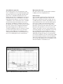
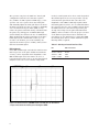
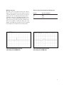
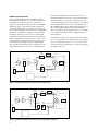
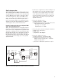
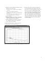
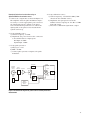
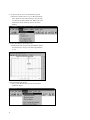
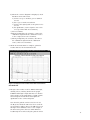
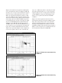
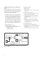
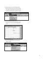
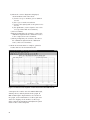
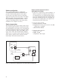
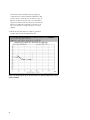
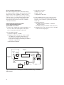
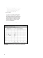
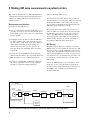
2. Making residual (two-port) measurements on pulsed carriers
This chapter presents the recommended procedures and hardware configurations for making
residual or two-port phase noise measurements
on pulsed carriers.
Residual measurement considerations
Phase detector selection
For carrier frequencies greater than the standard
input frequency range, another phase detector
must be used. This detector may be either an external phase detector (whose output would be routed
to the noise input port of the Agilent 70420A phase
noise test set) or an optional internal microwave
phase detector:
Standard (internal)
Option 201 (internal)
Option 001 (internal)
50 kHz–1.6 GHz
1.2 GHz–26.5 GHz
1.2 GHz–26.5 GHz
Path delay differences
When making pulsed carrier residual phase noise
measurements, the delay differences between the
two paths will normally not be a concern. If the
PRF (Pulse Repetition Frequency) is high, and
comparisons are being made to non-pulsed or CW
measurements, then the time delay difference in
the two paths between the power splitter and the
phase detector should be kept to a minimum. The
attenuation of the stimulus source’s noise is a
function of offset frequency (f) and the difference
in delay time (∆τ): stimulus source noise attenuation (dB) = 20 log (2 sin (πf ∆τ)). At f = 1/(2π ∆τ)
the attenuation goes to 0 dB and at 1/(2 ∆τ), there
is a 6 dB gain.
4
Measurement noise floor
The measurement noise floor represents the lowest
level of noise the system is capable of measuring.
For CW signals, it is set by the noise floor of the
phase detector, the LNA (Low-Noise Amplifier),
and the AM noise feedthrough. Additionally, for
pulsed carrier signals, the duty cycle of the pulsed
signal further degrades the CW noise floor by a
20*log (duty cycle) factor due to a scaling of the
effective detector constant by the duty cycle. The
noise of the phase detector is a function of the signal power present at the detector input ports. The
recommended power levels (CW or peak) for the
microwave phase detector, to ensure maximum
sensitivity (lowest noise floor), minimum DC offset
and minimum AM noise feedthrough, are +7 to
+10 dBm for the reference input port and 0 to
+5 dBm for the signal input port. The recommended
power levels (CW or peak) for the RF phase detector are +15 dBm for the reference port input and
+10 dBm for the signal input port.
Source AM noise
The stimulus source used for residual measurements must have low AM noise characteristics.
AM noise can cause AM-to-PM conversion within
the DUT (Device Under Test) and it can degrade
the overall measurement system noise floor.