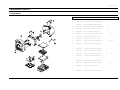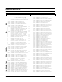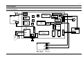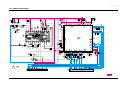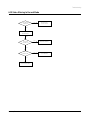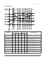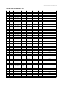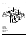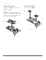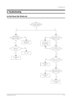
1
Television Video Cassette Recorder Chassis : Model : Television Video Cassette Recorder C15C ( VER.1, TS-10 ) TB14A53X/RAD CONTENTS 1. Precautions 2. Specifications 3. Disassembly and Reassembly 4. Alignment and Adjustment (Mechanical) 5. Alignment and Adjustment (Electrical) 6. Troubleshooting 7. Exploded View and Parts List 8. Electrical Parts List 9. Block Diagram 10. Wiring Diagram 11. Schematic Diagrams Precautions 1. Precautions Follow these safety, servicing and ESD precautions to prevent damage and protect against potential hazards such as electrical shock and X-rays. 1-1 Safety Precautions 1. Be sure that all of the built-in protective devices are replaced. Restore any missing protective shields. 2. When reinstalling the chassis and its assemblies, be sure to restore all protective devices, including: nonmetallic control knobs and compartment covers. 3. Make sure that there are no cabinet openings through which people—particularly children—might insert fingers and contact dangerous voltages. Such openings include the spacing between the picture tube and the cabinet mask, excessively wide cabinet ventilation slots, and improperly fitted back covers. If the measured resistance is less than 1.0 megohm or greater than 5.2 megohms, an abnormality exists that must be corrected before the unit is returned to the customer. 4. Leakage Current Hot Check (Figure 1-1): Warning: Do not use an isolation transformer during this test. Use a leakagecurrent tester or a metering system that complies with American National Standards Institute (ANIS C101.1, Leakage Current for Appliances), and Underwriters Laboratories (UL Publication UL1410, 59.7). 5. With the unit completely reassembled, plug the AC line cord directly into the power outlet. With the unit’s AC switch first in the ON position and then OFF, measure the current between a known earth ground (metal water pipe, conduit, etc.) and all exposed metal parts, including: antennas, handle brackets, metal cabinets, screwheads and control shafts. The current measured should not exceed 0.5 milliamp. Reverse the powerplug prongs in the AC outlet and repeat the test. Samsung Electronics LEAKAGE CURRENT TESTER DEVICE UNDER TEST (READING SHOULD NOT BE ABOVE 0.5mA) TEST ALL EXPOSED METAL SURFACES 3-WIRE CORD ALSO TEST WITH PLUG REVERSED (USING AC ADAPTER PLUG AS REQUIRED) EARTH GROUND Fig. 1-1 AC Leakage Test 6. Antenna Cold Check: With the unit’s AC plug disconnected from the AC source, connect an electrical jumper across the two AC prongs. Connect one lead of the ohmmeter to an AC prong. Connect the other lead to the coaxial connector. 7. X-ray Limits: The picture tube is especially designed to prohibit X-ray emissions. To ensure continued X-ray protection, replace the picture tube only with one that is the same type as the original. Carefully reinstall the picture tube shields and mounting hardware; these also provide X-ray protection. 8. High Voltage Limits: High voltage must be measured each time servicing is done on the B+, horizontal deflection or high voltage circuits. Correct operation of the X-ray protection circuits must be reconfirmed whenever they are serviced. (X-ray protection circuits also may be called “horizontal disable” or “hold-down”.) Heed the high voltage limits. These include the X–ray Protection Specifications Label, and the Product Safety and X-ray Warning Note on the service data schematic. 1-1 2. Specifications The descriptions and characteristics given in this booklet are given for information purposes only and are subject to modification without notice. TELEVISION PART Colour systems TV standards Number of channels Reception range/cable TV Aerial input VCR PART Format Heads Luminance Colour FF/REW time Wow and flutter (WTD) Frequency response GENERAL Power supply Consumption Audio output power Number of loudspeakers Tube size Tube type Sockets Dimensions (W x D x H) Weight Operating temperature Relative humidity Samsung Electronics PAL(option) / SECAM(option) (UK;PAL) L/L’(option), B/G(option), D/K(option) (UK;I) 100 programmes Hyperband/interband tuner 75 Ohms, coaxial cable VHS standard (PAL / SECAM(option) / MESECAM(option) / NTSC in playback only) Video: 2 rotary heads, LP(option), 4 Heads(option) Audio/Control: 1 stationary head (linear) Erase: 1 full track erase head System Video Normal CCIR System Audio Mono / NICAM&A2-STEREO FM azimuth recording Down converted subcarrier phase shifted direct recording Less than 100 seconds in FF with E-120 0.4% maximum (SP) 100 Hz - 8 KHz 220-240V~, 50Hz (110-260V~, 50/60Hz; option) 14” (60W) 20”/21” (90W) 14” (1.5W) 20” (3W) 21” (1.5Watts x 2) 14”/20” (1) 21” (2) 14” (37cm/34cmV) 20” (51cm/48cmV) 21” (55cm/51cmV) BLACK MATRIX 1 full RGB SCART on the rear 1 RCA input (audio and video) on the front Earphones output (3.5 mm mini-jack) 1 aerial/cable TV coaxial input 14” (368.5 x 388 x 381) 20” (488 x 477 x 488) 21” (520 x 495 x 508) 14” (11.7 kg) 20” (20.4 kg) 21” (23.2 kg) 5°C - 40°C (41°F - 104°F) 10% - 75% 2-1 Disassembly and Reassembly 3. Disassembly and Reassembly 3-1 Disassembly 3-1-1 Back Cover Removal 1. Remove the screws located on the side of the back cover. Samsung Electronics 3-1 4. Disassembly and Reassembly 4-1 Deck Parts Locations 4-1-1 Top View Œ ˇ ¨ ˆ ´ Ø Fig. 4-1 Top parts Location-1 Œ ´ ˇ ¨ ˆ Ø GEAR FL CAM MOTOR LOADING ASS’Y LEVER FL ARM ASS’Y HOLDER FL CASSETTE ASS’Y LEVER FL DOOR SLIDER FL DRIVE Samsung Electronics 4-1 Troubleshooting 6. Troubleshooting 6-1 No Power (No Picture on) Check both terminal voltages of C820 (125V) Yes No Check both terminal voltages of C807 (280~300V). Yes Is Q801 Pin 3 19~22V? Yes Check/Replace T801. No Check D801~804 F801,Q801. No No Check whether each power line is short or open. No Check IC801 Check Voltage of 5V, 6V, 8V, 13V power line.. Yes Is IC901 Pin 64 Voltage 5V? Yes No Check/Replace IC901. No Check/Replace IC902. Check H.V SYNC on IC901 Pins 1, 2 Yes Check IC901 Pin 3 is High when power is On. Yes Check the voltage of TU001. Samsung Electronics 6-1 Exploded View & Parts List 7. Exploded View & Parts List 7-1 TB14A53X/RAD Samsung Electronics No Code No Description;Specification Q’ty 1 AA91-00184D ASSY CABINET FRONT;-,14A5 MASTER,BK708P 1 AA64-31339P CABINET FRONT;14A5,C5,BK708P HITRON EL,H 1 1-1 AA64-70127F BADGE-BRAND;AL,SAMSUNG,SILVER,L40,R800,N 1 1-2 AA96-00149A ASSY-SPEAKER;-,-,16 OHM,2.5W,3001-001015 1 1-3 AA95-00630B ASSY-PCB,A/V;-,14/20/21,C15C,PAL,-,MO 1 1-4 6003-000333 SCREW-TAPTITE;RH,+,2S,M3,L10,ZPC(YEL),SW 2 1-5 AA64-00018A WINDOW-REMOCON;-,TVN-502V,-,PC,VIOLET,-, 1 1-6 AA64-00012A INDICATOR-LED;-,TVN-502V,-,PC,-,CLEAR,- 1 1-7 6003-000333 SCREW-TAPTITE;RH,+,2S,M3,L10,ZPC(YEL),SW 2 1-8 AA64-00051E PANEL CONTROL;14A5 MAST,HIPS,-,V0,BLK,-, 1 2 AA03-10002N CRT-COLOR;-,A34KQV42X,-300MG,14,90DEG,5 1 2-1 AA65-30016A CLAMP-D,COIL;-,NYLON-66,V0,-,NTR,DADH-36 2 2-2 AA60-10050R SCREW-ASSY;-,SWRCH18A,M5,L31.5,HH,+,WC,- 4 2-3 3704-000103 SOCKET-CRT;10P,22.5,14.3,SN,ISMS01S/BK 1 3 AA64-31340C CABINET-BACK;-,14A5,C5,SEA ,HIPS,V0,BLK 1 3-1 6002-000514 SCREW-TAPPING;RH,+,2,M4,L15,ZPC(BLK),SWR 4 3-2 AA42-00003A ANT ROD;-,3S,720mm,ABS,UL/CSA,- 1 4 AA96-20124A ASSY-POWER,CORD;-,EP2/YES(AU),H/C250,KJP 1 Remark AV+CF IND+CF CRT CB+CF 7-1 Electrical Parts List 8. Electrical Parts List 8-1 TB14A53X/RAD Loc. No. Code No. Description ; Specification Remark ASSY PCB MAIN(OPT) ! ! ! ! ! ! ! ! ! ! ! ! ! ! ! ! ! ! ! ! ! 1 * AA94-02669C ASSY PCB MAIN(OPT);TB14A53X/RAD,C15C,NEW ..2 ..2 ..2 ..2 ..2 ..2 ..2 ...3 ...3 ...3 ...3 ...3 ..2 ..2 ...3 ...3 ...3 ...3 ...3 ...3 ..2 ...3 ...3 ...3 ...3 ..2 ...3 ...3 ...3 ..2 ..2 ..2 ..2 ..2 ..2 ..2 ..2 ..2 ...3 ...3 ...3 ...3 ...3 ...3 ...3 ....4 ....4 ....4 ...3 ...3 ...3 ...3 ...3 ...3 ...3 ...3 ...3 ...3 ...3 ...3 ...3 ...3 ...3 C237 C807 CR402S CR403S GT02A HC002 IC301 2401-001840 C-AL;100uF,20%,16V,GP,TP,6.3x11,5 2401-002241 C-AL;220uF,+30-10%,400V,GP,ST,30x40 2301-001219 C-FILM,MPE-PPF;3.9nF,5%,1.6KV,TP,29x8.5x 2306-000188 C-FILM,MPPF;330nF,5%,400V,TP,26x19.5x11, AA39-20010B LEAD CONNECTOR-ASSY;,1P,YFH800-01,S,500, AA13-00087A IC HYBRID;-,TAR001,SIP,10P,-,BK AA96-50345E ASSY-H/S;-,VERT,AA62-30174A,TDA8356/N6A AA62-30174A HEAT SINK-PS;-,SPC,T1.0,-,33X20X50,-,FTAA61-10162A BRACKET-IC;-,SBHG-1,T1.0,-,-,-,6003-000334 SCREW-TAPTITE;RH,+,2S,M3,L6,ZPC(YEL),SWR 1204-001541 IC-VERTICAL DEF.;TDA8356/N6A,SIP,9P,-,PL 0205-000129 GREASE-SILICON;SC102,JAPAN 1201-001386 IC-POWER AMP;7267,DIP,16P,-,DUAL,32dB,PL AA96-50298C ASSY-H/S;-,POWER,AA62-30171A,KA3S0680,C AA63-30189A COVER-HEATSINK;-,-,AA62-30171,PC-ABS,V0, AA62-30171A HEAT SINK-ES;-,A6063 EXTR,-,-,-,WHT,40(3 AA61-10386A BRACKET-IC;-,SECC 100,T1.0,-,-,-,KA2S068 6003-000333 SCREW-TAPTITE;RH,+,2S,M3,L10,ZPC(YEL),SW 1203-001313 IC-PWM CONTROLLER;3S0680,TO-3P,5,150MIL, 0205-000129 GREASE-SILICON;SC102,JAPAN AA96-50407B ASSY H/S;-,VERTICAL,AA62-30154G,KA7806, 0205-000129 GREASE-SILICON;SC102,JAPAN 1203-000284 IC-POSI.FIXED REG.;7806,TO-220,3P,-,PLAS 6003-000333 SCREW-TAPTITE;RH,+,2S,M3,L10,ZPC(YEL),SW AA62-30154G HEAT SINK-ES;-,A6063 EXTR,-,WHT,50/16,-, AA96-50153H ASSY-H/S;-,-,AA62-30013D,KA78R09,1203-001225 IC-POSI.FIXED REG.;78R09,TO-220,4P,-,PLA 6003-000333 SCREW-TAPTITE;RH,+,2S,M3,L10,ZPC(YEL),SW AA62-30013D HEAT SINK-ES;-,A6063 EXTR,-,-,55(21) T02 1203-001752 IC-POSI.FIXED REG.;LF33CV,TO-220,3P,-,PL 3722-000161 JACK-PIN;2P,3.4mm,SN,BLK,AA27-20003U COIL-DEGAUSSING;-,14,16.4ohm,75T,890mm,D AA27-30001K COIL-LINEARLITY;-,230uH,DR1215,PI0.5,14. AA29-30001C FILTER-LINE NOISE;-,39mH,1.0A,-,AA26-00004A TRANS-FLYBACK;-,FSA38026S,14INCH,125V AA26-20007U TRANS-SWITCHING;-,90~260V,125V/16.5V/9.5 AA40-10006MTUNER-F/S;TECC2949PG29A(S),PAL-B/G,TR,18 AA99-30224S ASSY-PCB ROBOT; AA94-02669C ,ER 3711-003641 CONNECTOR-HEADER;BOX,12P,1R,2.5mm,STRAIG 3711-003641 CONNECTOR-HEADER;BOX,12P,1R,2.5mm,STRAIG 2306-000318 C-FILM,MPPF;220nF,20%,250V,TP,-,22.5mm 2306-000318 C-FILM,MPPF;220nF,20%,250V,TP,-,22.5mm 2201-000987 C-CERAMIC,DISC;2.2nF,20%,400V,Y5U,TP,12. 2201-000987 C-CERAMIC,DISC;2.2nF,20%,400V,Y5U,TP,12. AA96-00111C ASSY-H/S;-,-,AA62-30013L,FML-G12S,0402-000233 DIODE-RECTIFIER;FML-G12S,200V,5A,-,6003-000333 SCREW-TAPTITE;RH,+,2S,M3,L10,ZPC(YEL),SW AA62-30013L HEATSINK-ES;-,-,-,-,44/22,-,WHT,-,-,-,0402-000233 DIODE-RECTIFIER;FML-G12S,200V,5A,-,3601-000261 FUSE-CARTRIDGE;250V,3.15A,TIME-LAG,GLASS 1204-001440 IC-VIDEO SYSTEM;TDA8842,DIP,56P,300MIL,P 0801-000961 IC-CMOS LOGIC;4053,MUTIPLEXER,DIP,16P,30 0801-000213 IC-CMOS LOGIC;4052,MULTIPLEXER,DIP,16P,3 AA09-00088A IC MICOM;SAA5543PS/M4-0258,C15C,52P,3.3 1103-000118 IC-EEPROM;24WC08,1Kx8Bit,DIP,8P,300MIL,1 1404-001045 THERMISTOR-NTC;4.7ohm,15%,2900K,35.0mW,T 0604-001038 PHOTO-COUPLER;TR,130-260%,200mW,DIP-4,ST 1404-000002 THERMISTOR-PTC;9ohm,20%,-,-,TR,RECT,0502-001115 TR-POWER;KSC5386,NPN,50W,TO-3PF,ST,83501-001040 RELAY-POWER;12VDC,500mW,10A,1FormA,15mS, 2904-001239 FILTER-SAW AV;38.9MHz,SIP5K,ST,16.3dB,B/ AA26-50001B TRANS-HORIZ.DRIVE;-,7.1mH,102uH,10-20uH, AA99-10218N ASSY-PCB MAIN,AUTO; AA99-30224S ,V IC601 IC801S IC804 IC806 IC903 JS701 L803 LR401S LX801S T444S T801S TU01S CN101 CN102 CX801S CX802S CY801S CY802S D818 D820 FP801S IC201S IC701 IC702 IC901S IC902S NT801S PC801S PT801S Q401 RL801S SF101S T401 Samsung Electronics S.N.A S.N.A S.N.A S.N.A S.N.A S.N.A S.N.A S.N.A S.N.A S.N.A S.N.A S.N.A S.N.A S.N.A S.N.A S.N.A S.N.A S.N.A S.N.A Loc. No. ....4 ....4 ....4 ....4 ....4 ....4 ....4 ....4 ....4 ....4 ....4 ....4 ....4 ....4 ....4 ....4 ....4 ....4 ....4 ....4 ....4 ....4 ....4 ....4 ....4 ....4 ....4 ....4 ....4 ....4 ....4 ....4 ....4 ....4 ....4 ....4 ....4 ....4 ....4 ....4 ....4 ....4 ....4 ....4 ....4 ....4 ....4 ....4 ....4 ....4 ....4 ....4 ....4 ....4 ....4 ....4 ....4 ....4 ....4 ....4 ....4 ....4 ....4 ....4 ....4 ....4 ....4 ....4 C101 C102 C107 C108 C109 C112 C201 C202 C204 C205 C206 C207 C208 C209 C210 C211 C212 C213 C214 C215 C219 C221 C222 C225 C226 C227 C228 C230 C231 C232 C233 C234 C236 C238 C239 C249 C250 C251 C253 C254 C255 C257 C260 C261 C262 C265 C301 C302 C303 C304 C305 C306 C307 C308 C401 C405 C406 C407 C408 C409 C411 C412 C413 C414 C415 C601 C602 C604 Code No. 2401-000030 2202-000127 2202-000807 2401-000962 2202-000632 2305-000196 2401-002619 2305-000412 2301-000224 2401-000660 2306-000122 2401-001840 2305-000412 2305-000289 2305-000412 2301-000232 2306-000122 2306-000122 2306-000122 2401-000480 2201-000273 2306-000122 2401-001840 2401-000603 2401-000603 2202-000796 2309-000138 2401-002144 2401-000480 2202-000849 2202-000243 2301-000445 2301-000232 2301-000383 2401-000603 2401-000480 2306-000122 2306-000122 2202-000210 2202-000127 2401-002619 2202-000791 2202-000121 2301-000192 2202-000210 2401-002144 2202-000796 2401-002293 2305-000149 2305-000285 2202-000796 2401-002288 2305-000285 2305-000407 2301-000383 2305-000704 2201-000556 2401-002288 2201-000556 2401-001661 2201-000556 2401-000927 2401-003028 2201-000639 2305-000382 2401-001998 2305-000665 2401-002619 Description ; Specification Remark C-AL;22uF,20%,25V,GP,TP,5x11,5 C-CERAMIC,MLC-AXIAL;10nF,+80-20%,25V,Y5V C-CERAMIC,MLC-AXIAL;22nF,+80-20%,25V,Y5V C-AL;22uF,20%,50V,GP,TP,5x11,5 C-CERAMIC,MLC-AXIAL;100nF,20%,50V,Z5U,TP C-FILM,MPEF;150nF,5%,63V,TP,-,5mm C-AL;47uF,20%,25V,GP,TP,5x11,5 C-FILM,MPEF;470nF,5%,63V,TP,-,5mm C-FILM,PEF;22nF,5%,50V,TP,7.4x3.9x13mm,5 C-AL;2.2uF,20%,50V,GP,TP,5x11,5 C-FILM,MPPF;100nF,5%,50V,TP,7.3x4.0x5.0m C-AL;100uF,20%,16V,GP,TP,6.3x11,5 C-FILM,MPEF;470nF,5%,63V,TP,-,5mm C-FILM,MPEF;220nF,5%,63V,TP,-,5mm C-FILM,MPEF;470nF,5%,63V,TP,-,5mm C-FILM,PEF;3.3nF,5%,50V,TP,8.1x4.5x13mm, C-FILM,MPPF;100nF,5%,50V,TP,7.3x4.0x5.0m C-FILM,MPPF;100nF,5%,50V,TP,7.3x4.0x5.0m C-FILM,MPPF;100nF,5%,50V,TP,7.3x4.0x5.0m C-AL;10uF,20%,50V,GP,TP,5x11,5 C-CERAMIC,DISC;0.018nF,5%,50V,NP0,TP,5x3 C-FILM,MPPF;100nF,5%,50V,TP,7.3x4.0x5.0m C-AL;100uF,20%,16V,GP,TP,6.3x11,5 C-AL;1uF,20%,50V,GP,TP,5x11,5 C-AL;1uF,20%,50V,GP,TP,5x11,5 C-CERAMIC,MLC-AXIAL;1NF,10%,50V,Y5P,TP,3 C-FILM,PE-PPF;100nF,5%,50V,TP,20x16x8.5, C-AL;47uF,20%,16V,GP,TP,5x11,5 C-AL;10uF,20%,50V,GP,TP,5x11,5 C-CERAMIC,MLC-AXIAL;18pF,5%,50V,CH,TP,3. C-CERAMIC,MLC-AXIAL;33pF,5%,50V,SL,TP,3. C-FILM,PEF;4.7nF,5%,50V,TP,5.5x7x3mm,5mm C-FILM,PEF;3.3nF,5%,50V,TP,8.1x4.5x13mm, C-FILM,PEF;10nF,5%,50V,TP,6x7x3.2mm,5mm C-AL;1uF,20%,50V,GP,TP,5x11,5 C-AL;10uF,20%,50V,GP,TP,5x11,5 C-FILM,MPPF;100nF,5%,50V,TP,7.3x4.0x5.0m C-FILM,MPPF;100nF,5%,50V,TP,7.3x4.0x5.0m C-CERAMIC,MLC-AXIAL;270PF,10%,50V,Y5P,TP C-CERAMIC,MLC-AXIAL;10nF,+80-20%,25V,Y5V C-AL;47uF,20%,25V,GP,TP,5x11,5 C-CERAMIC,MLC-AXIAL;150pF,10%,50V,Y5P,TP C-CERAMIC,MLC-AXIAL;100pF,10%,50V,Y5P,TP C-FILM,PEF;1nF,5%,50V,TP,5.3x10mm,5mm C-CERAMIC,MLC-AXIAL;270PF,10%,50V,Y5P,TP C-AL;47uF,20%,16V,GP,TP,5x11,5 C-CERAMIC,MLC-AXIAL;1NF,10%,50V,Y5P,TP,3 C-AL;68uF,20%,100V,WT,TP,10x20,5 C-FILM,MPEF;100nF,5%,100V,TP,12x12.5x6.5 C-FILM,MPEF;220NF,5%,100V,TP,10.5X5.5X15 C-CERAMIC,MLC-AXIAL;1NF,10%,50V,Y5P,TP,3 C-AL;470uF,20%,25V,WT,TP,10x20,5 C-FILM,MPEF;220NF,5%,100V,TP,10.5X5.5X15 C-FILM,MPEF;470nF,5%,100V,TP,-,5mm C-FILM,PEF;10nF,5%,50V,TP,6x7x3.2mm,5mm C-FILM,MPEF;100nF,5%,250V,TP,16.5x10.3x5 C-CERAMIC,DISC;0.47nF,10%,500V,Y5P,TP,5. C-AL;470uF,20%,25V,WT,TP,10x20,5 C-CERAMIC,DISC;0.47nF,10%,500V,Y5P,TP,5. C-AL;68uF,20%,100V,GP,TP,10x16,5 C-CERAMIC,DISC;0.47nF,10%,500V,Y5P,TP,5. C-AL;22uF,20%,250V,GP,TP,13x20,5 C-AL;100uF,20%,25V,WT,TP,6.3x11,5 C-CERAMIC,DISC;0.68nF,10%,2kV,Y5P,TP,9x5 C-FILM,MPEF;4.7nF,5%,400V,TP,-,5mm C-AL;1000uF,20%,25V,GP,TP,10x20,5mm C-FILM,MPEF;100nF,5%,63V,TP,7.5x4.0x5.0m C-AL;47uF,20%,25V,GP,TP,5x11,5 8-1 Block Diagrams 9. Block Diagrams 9-1 C15C Video Block Diagram 9-1-1 Notes The TV’s 1st and 2nd tuners (and VCR module) are “multi-system.” compatible: IC201 (TDA8842/8841) is the video, chroma, and deflection (VCD) IC . 9-1-1(A) TAPE PLAYBACK (REGARDLESS OF ORIGINAL RECORDING SYSTEM) If the output PB signal of micom pin 6 is high, the PB signal outputs from module deck 2, passes through IC 702 pins 2 and 3 and out to another VCR . The output signal of IC701 pin 1 (pin 15) outputs from IC201S pin 17 . 9-1-1(B) VIEWING NORMAL CHANNEL WHILE RECORDING A SCRAMBLED CHANNEL: The output CVBS (Composite Video Signal) of the 2nd IF outputs to IC702pin 3 when the micom’s pin 7 V/T/H (VCR tuner high) is high . The decoded signal goes to IC701 pin 2, where it is fed to IC 701 pin 4 (high output of micom’s’ pin 8— AV/Tuner), and out to VCR pin 4 (module deck) for recording. 9-1-1(C) VIEWING A SCRAMBLED CHANNEL WHILE RECORDING AN UNSCRAMBLED CHANNEL. The output CVBS of the 2nd IF is fed from IC701 pin 5 to IC701 pin 4 (low output of micom pin 8—AV/tuner). Then it goes to the module deck pin 4 for recording. The scrambled signal (CVBS) is fed to IC702 pin 1 through the 1st IF, and then to IC702 pin 3 (micom’s pin 7, V/T/H registers low). Then it goes to the decoder input. The descrambled signal goes to IC701 pins 2 and 15 (PH high output of micom’s pin 6), and then to IC201S pin 17, where it outputs as RGB. 9-1-1(D) SYNCHRONOUS RECORDING: The viewer sees the signal from the 1st tuner , while the signal from the second tuner is recorded. Audio processing for the French system type is shown in the table. Samsung Electronics 9-1 Wiring Diagram 10. Wiring Diagram 10-1 C15C Wiring Diagram Samsung Electronics 10-1 Schematic Diagrams 11. Schematic Diagrams 11-1 VCR (SECAM BLOCK) : Power Line : Signal Line Samsung Electronics 11-1 Schematic Diagrams 11-2 VCR (SYSTEM BLOCK) TP1 TP1 TP6 TP4 TP5 TP2 TP2 TP3 TP3 TP4 TP5 TP6 11-2 Samsung Electronics Schematic Diagrams 11-3 VCR (A/V BLOCK) TP1 TP3 TP2 TP3 TP4 TP5 TP4 TP5 TP2 TP1 Samsung Electronics 11-3 Schematic Diagrams 11-4 VCR (POWER BLOCK) : Power Line : Signal Line 11-4 Samsung Electronics Schematic Diagrams 11-5 TV MAIN (1/4) TP1 TP2 TP3 TP4 TP5 : Power Line : Signal Line Samsung Electronics 11-5 Schematic Diagrams 11-6 TV MAIN (2/4) TP1 TP5 TP4 TP2 TP3 TP6 TP3 TP4 TP2 TP1 TP5 TP6 : Power Line : Signal Line 11-6 Samsung Electronics Schematic Diagrams 11-7 TV MAIN (3/4) TP 8 TP12 TP1 TP2 TP 7 TP11 TP3 TP4 TP5 TP6 : Power Line : Signal Line Samsung Electronics 11-7 Schematic Diagrams 11-8 TV MAIN (4/4) : Power Line : Signal Line 11-8 Samsung Electronics Schematic Diagrams 11-9 TUNER-IF NICAM(STEREO) : Power Line : Signal Line Samsung Electronics 11-9 Schematic Diagrams 11-10 2’nd IF(STEREO) : Power Line : Signal Line 11-10 Samsung Electronics Schematic Diagrams 11-11 IF (MONO) 11-12 CRT 11-13 2'nd IF PAL/SECAM-B/G, D/K, I OPTION (MONO) TP3 TP2 TP1 TP1 TP2 TP3 : Power Line : Signal Line Samsung Electronics 11-11 Schematic Diagrams 11-15 CONTROL 11-14 MASTER 11-16 FRONT-A/V (MONO) 11-17 FRONT-A/V (STEREO) : Power Line : Signal Line 11-12 Samsung Electronics Schematic Diagrams 11-18 Voltages (VTR) ICM301 1 ICM901 PLAY REC STOP 2.5 2.5 2.5 34 PLAY REC STOP 1.8 1.8 1.8 67 PLAY REC STOP 4 4 4 ICM602 ICM601 5 3 4 5 5 4 0 69 5 0 0 70 5 5 36 0 5 5 37 0 5 5 0 5 5 4 2 0 0 3 2 0 0 0 2 68 35 0 0 0 0 2 0.8 0 0 5 0.8 0 0 5 4 5 0 5 1 67 34 1 STOP STOP STOP STOP REC REC REC REC PLAY PLAY PLAY PLAY PLAY REC STOP 1 0.9 0.9 0 2 2 2.6 2.6 0 4 4 3 5.2 5.2 5.2 3.5 3.5 3.5 4 2.6 2.6 2.6 2 2.5 2.5 2.5 35 3.5 3.5 3.5 68 0 0 0 3 2.5 2.5 2.5 36 1.8 1.8 2 69 0.7 0.7 0.7 4 2.5 2.5 2.5 37 4.9 4.9 5 70 2 2 2 5 2.5 2.5 0 38 1.8 1.8 1.8 71 2.5 2.5 2.5 6 2.5 2.5 2.5 39 4 4 4 72 0.3 2.5 3 5 5 5 5 38 5 5 5 71 0 0 0 7 2.5 2.5 2.5 40 5 5 5 73 2.5 2.5 3.5 6 5 5 5 39 5 5 5 72 1.8 1.8 1.8 5 0 0 0 5 2.6 2.6 2.6 8 0 0 0 41 2.7 2.7 3 74 2 0 2 7 5 5 5 40 0 0 0 73 0 0 0 6 0 0 0 6 2.6 2.6 2.6 9 0 0 0 42 3 3 3.2 75 5 5 5 8 5 5 5 41 5 5 5 74 0 0 0 7 0 0 0 7 5 5 0 10 1.6 1.6 2 43 1.9 1.9 2 76 2.5 2.5 2.5 9 5 5 0 42 5 5 5 75 0 0 0 11 3.2 3.2 3.2 44 4.3 4.3 0 77 0 0 0 10 5 5 0 43 5 5 5 76 0.7 0.7 0.7 8 2.5 2.5 2.5 8 5 5 0 12 5 2 2.5 45 1.8 1.8 2 78 2.5 2.5 0 11 0 0 0 44 5 5 5 77 0.7 0.7 0.7 9 2.5 2.5 2.5 9 12.5 2.5 0 0 0 45 0 0 0 78 0 0 0 10 2.5 2.5 2.5 10 13 0 0 0 46 0 0 0 79 0 0 0 14 5 5 5 47 0 0 0 80 0 0 0 11 2.5 2.5 2.5 11 0 5 12.5 0 13 12 5 5.1 15 3.5 3.5 3.5 48 5 5 5 81 3 0 0 12 4.5 4.5 4.5 12 5 5 5.1 16 4.5 4.5 4.5 49 5 5 5 82 4 0 0 13 2.5 2.5 2.5 13 0 0 14 2.5 4.7 4.5 14 0 0 0 0 1.5 79 2 9 80 2.5 5 2.5 2.3 2.2 81 0 0 0 1.2 1 82 1.8 4.1 1 0 0 0 83 0 0 0 17 0 0 0 50 5 5 5 83 0 0 0 51 1.9 1.9 0 84 1.8 4.1 1 18 4.5 4.5 4.5 51 5 5 5 84 0 0 0 52 2.4 2.4 2.5 85 1.8 4.1 1 19 3.5 3.5 3.5 52 5 5 5 85 2.5 5 2.5 15 3 2.5 2.5 15 0 0 0 0 0 20 5 5 5 53 5 5 5 86 2.5 5 2.5 16 5 1 1 16 8.4 8.8 17 2.5 2.5 2.5 17 8.4 8.8 13 1.5 1.5 2 46 1.5 14 1.5 1.5 1.6 47 2 15 2.2 2.2 2.2 48 2.3 16 5 5 5 49 1.2 17 3 0 0 50 18 1.8 2.1 2.2 19 2.1 2.1 2.2 1.4 2.5 2.5 0 0 0 20 2.8 2.8 3.2 53 0 0 0 86 21 2.1 2.1 2.5 54 2.4 2.4 2.5 87 5 5 5 21 0 0 0 54 5 5 5 87 2.5 2.5 2.5 22 0 0 0 55 5 5 5 88 1.8 4.1 2 22 0 0 0 55 0 5 0 88 2.5 2.5 2.5 23 5 5 5 56 3.5 3.5 0 89 0 0 0 23 5 5 0 56 0 0 0 89 2.5 2.5 2.5 18 2 2 2 18 8.4 8.8 0 0 2.5 2.5 2.5 19 2.5 2.5 2.5 19 5.2 5.2 0 20 2.5 2.5 2.5 20 0 0 0 24 5 5 5 57 3.4 3.4 3.5 90 1.8 4.1 2 24 5 5 0 57 0 0 0 90 25 5 5 0 58 5 5 5 91 0 0 0 26 0 0 0 59 5 5 5 92 5 5 5 27 5 5 5 60 5 5 5 93 5 5 5 21 2.5 2.5 2.5 21 12.5 12.5 13 8.2 8.2 0 8.2 0 25 1.8 1.8 2.8 58 5 5 5 91 1.8 4.1 2 26 0.8 0 1 59 3.4 3.4 3.5 92 4 1.6 0 27 4.1 4.1 4.1 60 3.5 3.5 3.5 93 4 4.0 0 28 5 5 5 61 5 5 5 94 0 5 0 22 5 5 5 22 8.4 28 4.1 4.1 4.1 61 3.3 3.3 3.5 94 0.5 0.7 0 29 5 5 0 62 0 0 0 95 0 0 0 29 0.8 0.8 3 62 3.5 3.5 3.5 95 0 0 0 23 3 3 3 23 30 0 0 0 63 0 0 0 96 5 5 5 30 1 0 1 63 4 4 0 96 2.5 2.5 2.5 31 0 0 0 64 5 5 5 97 5 5 5 24 3 3 3 24 8.4 8.4 31 2.1 2.1 3.5 64 2.2 2.2 0 97 0 0 0 32 5 5 5 65 0 0 0 98 5 5 0 25 4.1 3 3 25 1.8 1.8 2.6 32 1.8 1.8 2 65 2.4 2.4 2.2 98 2.5 2.5 2.5 33 0 0 0 66 0 5 0 99 5 5 0 26 5 0 0 26 1.8 2 2 1.5 66 2.5 2.5 3 99 5 4.3 5 100 5 5 5 27 4.1 4.1 4.1 27 100 2.5 2.5 2.5 1.4 1.8 1.4 0 33 28 3.1 3.1 3.1 28 2.4 2.5 2 27 5.2 0 5.2 0 0 0 28 Samsung Electronics 0 1 11-13 Schematic Diagrams 11-19 Voltages (TV) Q801 KA3S0680RF : Units : Volts PIN NO PIN NAME ST AND-BY POWER ON 1 DAR.IN 299 290 2 GND - - 3 VCC 19.5 20.3 4 VFB 0.2 1.3 5 SYNC 0.8 6.7 IC902 PC123Y : Units : Volts PIN NO ST AND-BY POWER 1 16.5 16.7 2 15.4 15.7 3 GND GND 4 0.2 1.3 IC501 TDA6107Q : Units : Volts IC901 SAA5554PS-OTP Units : Volts PIN NO PIN NAME VOL T AGES(V ) 1~4 GND - PIN NO PIN NAME VOL T AGES(V) PIN NO PIN NAME VOL T AGES(V ) S-L CTL - 37 N.C - 5 SDA 4.8 1 6 SCL 4.8 2 BUS-STOP 5.2 38 GND - 7 GND - 3 D-coil - 39 GND - 8 VDD 5.2 4 ST BY-REC - 40 S-MUTE 2.8 5 PB-L - 41 VDD 3.2 6 AV-L 0.67 42 OSD B - 0.67 43 OSD G - OSD R - : TDA7267A Units : Volts PIN NO PIN NAME VOL T AGES(V ) 1 VS 1.6 2 OUT 8.5 3 SVR 8.7 4 IN 0.8 5 N.C - 6 S-GND - 7~8 N.C - 9~16 P-GND - 7 VT-L 8 HOLD 2.48 44 9 1T/AFT 3.2 45 F/B - 10 2T/AGC 2.7 46 H-SYNC 0.79 11 2T/AFT 3.2 47 V-SYNC - 12 SCART-ID - 48 VSSP - 13 GND - 49 VDD 3.2 14 BG/I - 50 GND - 15 D/K - 51 Xtal 1.6 PIN NO PIN NAME VOL TAGE S(V ) 16 1TS-L H 5.2 52 Extal 1.6 1 B-IN 2.4 17 S-L H 4.9 53 RESET - 2 R-IN 2.4 18 FRA-H 3.7 54 VDD 3.2 3 G-IN 2.5 19 LNA 4.4 55 REMOCON 5.2 4 GND - 20 TV PWR 3.2 56 TV CLK 5.1 5 lom 5.4 21 PB MUTE - 57 V-SYNC INTER - 6 Vdd 166 22 VSSA - 58 TV SI - 7 G-OUT 90~115 23 CVBS0 0.2 59 TV SO 1.0 8 R-OUT 93~118 24 CVBS1 1.3 60 TV CS - 9 B-OUT 97~119 25 BLACK 0.48 61~62 SCL 2.3 IREF 1.3 63~64 SDA 2.2 26 IC301 11-14 : Units : Volts IC601 IC801 24C08,24C04,24C16 : : TDA8356 Units : Volts PIN NO PIN NAME VOL T AGES(V ) 1 VD-INPUT 2.2 2 VD+INPUT 2.2 3 VCC 16.9 4 OUTPUT 8.2 5 GND - 6 VFB 41.5 7 OUT 8.5 8 VO - 9 VI 8.2 Samsung Electronics Schematic Diagrams 11-20 Voltages (TV) L OC IC101* IC101* IC TDA9818 2T-IF(F) LA7565B 2T-IF(W) PIN NO 1 3.3 2.0 IC701 TC4053BP - IV702 TC4052BP 1.6 ICL 01* STV8225 4.2 2 3.3 2.2 - 0.5 3.2 3 - 7.4 - 1.6 - 4 2.0 8.0 1.1 - 0.6 5 6 7 8 2.1 3.9 1.7 2.4 8.9 3.8 3.2 2.7 1.1 - 2.2 - 4.3 3.5 4.3 6.3 9 2.3 3.7 0.8 0.8 4.3 10 2.3 2.7 0.8 0.8 3.5 11 1.6 8.3 0.8 - 4.3 12 13 14 2.0 2.7 4.2 8.3 0.3 7.9 2.2 2.1 4.0 3.4 2.2 15 1.4 - - 0.4 16 1.9 - 8.9 8.9 17 0.4 2.9 18 19 20 21 2.6 2.6 4.9 3.4 3.4 1.7 22 0.8 2.4 23 3.2 3.3 24 3.2 Samsung Electronics 3.3 9.0 4.3 4.3 IC201 : TDA8842/8841 Units : Volts PIN NO PIN NAME VOL TAGE S(V ) P I N NO 1 SOUND IF INPUT - 31 B-Y OUTPUT - 2 EXT.AUDIO INPUT 3.6 32 R-Y OUTPUT - 3 N.C - 33 P I N NA M E SUBCARRIER V O L T A G E S(V ) OUTPUT - 4 N.C - 34 X-TAL(3.58) 2.4 5 PLL LOOPFILTER 2.4 35 X-TAL(4.43/3.58) 2.4 6 IF VIDEO OUTPUT 3.2 36 7 SCL 4.8 37 POSITIVE 8 SDA 4.8 38 CVBS 9 BANDGAP DECOUPLING 6.6 39 DECDIG 4.9 10 CHROMA INPUT - 40 HOR OUTPUT 0.3 11 Y/CVBS INPUT 3.3 41 12 MAIN POSITIVE SUPPLY 8.0 42 13 INT.CVBS INPUT 3.9 43 14 GND - 44 15 AUDIO OUT 3.0 45 16 SECAM DECOUPLING - 46 VERT.DRIVE POS 2.2 17 EXT.CVBS INPUT 3.3 47 VERT.DRIVE NEG 2.2 18 BLACK CURRENT INPUT 5.0 48 IF INPUT 4.5 19 BLUE OUTPUT 3.0 49 IF INPUT 4.5 20 GREEN OUTPUT 3.2 50 21 RED OUTPUT 3.2 51 VERT.SAWTOOTH 22 V-GUARD INP / BEAM CUR.LIMITTER 2.0 52 REFERENCE 23 RED INPUT 3.4 53 24 GREEN INTPUT 3.4 54 25 BLUE INTPUT 3.4 55 26 RGB INSERTION SWITCH INP 0.1 56 27 LUMINANCE INPUT 2.6 28 LUMINANCE OUTPUT 2.6 29 B-Y OUTPUT - 30 R-Y OUTPUT - LOOPFILTER BURST SANDCASTLE PHASE DET 4.9 SUPPLY 8.0 OUTPUT 2.7 OUTP/FLY-BACK PHI2 FILTER INP / FLASHPROT 3.2 PHI1 FILTER 3.9 GND EAST-WEST AGC - DRIVE/AVL EHT/OVERVOLTAGE 0.5 OUTPUT PROTECTION CAPACITOR CURRENT INPUT - INP 2.1 3.7 3.8 DECOUPLING CAPACITOR 4.2 TUNER INPUT 4.4 DEEMPHASSIS 2.8 AUDIO DECOUPLING AGC SOUND DEMODULATOR 2.4 11-15 Wiring Diagram 10-2 C15C Wiring Diagram 10-2 Samsung Electronics Block Diagrams 9-2 C15C Video Block Diagram (Continued) ANT MICOM#24 SDA MICOM #23 SCL ICT01 TTX #8 7 IC201 8 38 R 1st IF 1st Tunning CRT Drive G IF DET. B INT EXT 17 13 6 IC702 9 PB H Micom #6 2 10 V/T/H Micom #7 1 3 Trap 1T.option 2nd IF 2nd Tunning 5 C15A OPTION 15 IC701 V-in PB H 11 10 Micom #6 1 #13 L H 5 2 V-out VCR or Decorder 3 VPS ICP01 Micom #8 CN101 PB.V Module DECK 9 2 4 AV/Tuner 4 CN101 REC. SOURCE V. Micom Pin Function PIN NO. 6 7 8 56, 57 23,24 9-2 PIN NAME PB H V/T/H AV/TUNER FUNCTION High Output : Playback signal is monitored. The PB signal is output at scart. High Output : The second tuner signal is output at scart. High Output : AV signal is recorded. Low output : TUNER signal is recorded. S-L H FRA H FRA H Port S-L H S L L PAL/SEC L H FRANCE-L H L FRANCE-L' a C. SYSTEM : PAL/SEC ARE AUTO mode, and France is SECAM mode. Extra control signals are all controlled by the I2C bus. Select INT/EXT FRENCH system modulation SDA,SCL Samsung Electronics Block Diagrams 9-3 C15C Audio Block Diagram (MONO) ANT MICOM#24 SDA MICOM #23 SCL 7 8 IC201 SPK 1st IF 1st Tunning 15 IF PROCESS INT 6 EXT A 2 55 14 ZK01 ZK02 2nd IF A-0 2nd Tunning 1 IC701 HC002 13 11 H Micom #5 C15COPTION MICOM14 BG/I L MICOM15 DK/L 12 S/L (AM) EXT ZK03 ZK04 A out REC. SOURCE A.(TUNER) A in CN101 8 Module DECK 6 10 REC. SOURCE A.(EXT) PB.A EXT.A IF IN 11 S-L CTL 1T Switch 1T.A 9 om pti .o 7 B Micom #17 VCR or Decoder 14 12 9 H 15 10 H 10 (AM) S-L A C 5 1T.A B/G (FM) 13 L L Micom #5 Micom #7 IC702 Micom Pin Function PIN NO. 6 7 8 60 53,54 Samsung Electronics PIN NAME PB H V/T/H AV/TUNER S-L CTL a :S-L(AM) b : B/G (FM) c :EXT SDA, SCL BG/I L DK/L FUNCTION High output : PB audio is monitored. The PB audio is output at scart. High output : The second tuner audio is output at a scart. High output : AV audio is recorded. Low output : TUNER audio is recorded. 1 1.8 ~ 2.6V : In TV FM Mode, connect pin 7 to A and pin 9 to C. 2 4.1 ~ 4.9V : In TV AM Mode, connect pin 7 to A and pin 9 to A. 3 6.4 ~ 7.2V : In AV-AM Mode, connect pin 7 to B and pin 9 to A. 4 More than 7.3V : In AV-FM Mode, connect pin 7 to B and pin 9 to C. S AUTO BG DK I Port B/G D/K L L H L L H L H 9-3 Block Diagrams 9-4 C15C Audio Block Diagram (Only Stereo) ANT OPTION EXT- L 2F TDA EXT- R 1 Tuner 7297 Nicam Module INT- L MSP 3410 IC601 INT- R IC602 SCL 2Tuner L 2Tuner R EXT- L EXT- R SDA MICOM PB PB L R Decoder 2Tuner REC - L IF Module REC - R Module EXT- L Deck EXT- R TDA9874 9-4 Samsung Electronics Electrical Parts List Loc. No. ....4 ....4 ....4 ....4 ....4 ....4 ....4 ....4 ....4 ....4 ....4 ....4 ....4 ....4 ....4 ....4 ....4 ....4 ....4 ....4 ....4 ....4 ....4 ....4 ....4 ....4 ....4 ....4 ....4 ....4 ....4 ....4 ....4 ....4 ....4 ....4 ....4 ....4 ....4 ....4 ....4 ....4 ....4 ....4 ....4 ....4 ....4 ....4 ....4 ....4 ....4 ....4 ....4 ....4 ....4 ....4 ....4 ....4 ....4 ....4 ....4 ....4 ....4 ....4 ....4 ....4 ....4 ....4 ....4 ....4 ....4 ....4 ....4 ....4 ! ....4 ....4 ....4 8-2 Code No. C605 C606 C607 C608 C701 C702 C703 C704 C705 C706 C708 C710 C711 C715 C717 C724 C725 C726 C729 C730 C804 C805 C806 C808 C810 C811 C812 C813 C815 C816 C819 C820 C822 C823 C824 C825 C827 C828 C829 C830 C831 C832 C835 C839 C840 C844 C850 C853 C901 C902 C903 C904 C905 C907 C908 C909 C910 C911 C912 C913 C915 C916 C918 C919 C920 C921 C922 C923 CB03 CK02 CN501C CN601 CN701 CN702 CR401S CW901 D102 Description ; Specification 2301-000445 2401-000603 2401-000914 2401-001998 2401-000471 2401-001989 2202-000121 2202-000121 2401-002463 2202-000121 2401-002144 2401-000471 2401-000480 2401-002619 2401-000471 2401-001989 2401-000480 2401-002619 2401-000480 2401-000480 2401-002619 2401-002300 2301-000310 2301-001435 2301-000224 2301-000192 2201-000374 2201-000991 2201-000991 2201-000991 2401-000293 2401-000293 2401-002300 2401-001840 2401-002463 2401-002215 2306-000122 2401-002463 2401-002144 2401-001840 2401-002463 2306-000122 2401-002291 2401-002215 2306-000122 2401-002594 2401-001176 2401-001397 2202-000632 2306-000122 2202-000796 2401-000590 2201-000980 2201-000980 2401-002144 2202-000632 2401-003102 2401-001333 2202-000632 2401-002144 2301-000188 2401-000480 2202-000632 2202-000632 2305-000355 2202-000791 2202-000791 2202-000796 2202-000127 2202-000121 3711-002648 3711-002642 3711-002648 3711-002644 2201-002028 2503-000156 0401-000005 Remark C-FILM,PEF;4.7nF,5%,50V,TP,5.5x7x3mm,5mm C-AL;1uF,20%,50V,GP,TP,5x11,5 C-AL;22uF,20%,16V,GP,TP,5x11,5 C-AL;1000uF,20%,25V,GP,TP,10x20,5mm C-AL;10uF,20%,50V,BP,TP,5x11,5mm C-AL;4.7uF,20%,50V,BP,TP,5x11,5 C-CERAMIC,MLC-AXIAL;100pF,10%,50V,Y5P,TP C-CERAMIC,MLC-AXIAL;100pF,10%,50V,Y5P,TP C-AL;470uF,20%,16V,GP,TP,8x11.5,5 C-CERAMIC,MLC-AXIAL;100pF,10%,50V,Y5P,TP C-AL;47uF,20%,16V,GP,TP,5x11,5 C-AL;10uF,20%,50V,BP,TP,5x11,5mm C-AL;10uF,20%,50V,GP,TP,5x11,5 C-AL;47uF,20%,25V,GP,TP,5x11,5 C-AL;10uF,20%,50V,BP,TP,5x11,5mm C-AL;4.7uF,20%,50V,BP,TP,5x11,5 C-AL;10uF,20%,50V,GP,TP,5x11,5 C-AL;47uF,20%,25V,GP,TP,5x11,5 C-AL;10uF,20%,50V,GP,TP,5x11,5 C-AL;10uF,20%,50V,GP,TP,5x11,5 C-AL;47uF,20%,25V,GP,TP,5x11,5 C-AL;47uF,20%,50V,GP,TP,6.3x11,5 C-FILM,PEF;68nF,5%,50V,TP,8.0X8.5X4.0X5, C-FILM,PPF;1.5nF,5%,1.2kV,TP,15x8x12.5mm C-FILM,PEF;22nF,5%,50V,TP,7.4x3.9x13mm,5 C-FILM,PEF;1nF,5%,50V,TP,5.3x10mm,5mm C-CERAMIC,DISC;0.22nF,5%,50V,NP0,TP,10.5 C-CERAMIC,DISC;0.56nF,10%,2kV,Y5P,TP,7.5 C-CERAMIC,DISC;0.56nF,10%,2kV,Y5P,TP,7.5 C-CERAMIC,DISC;0.56nF,10%,2kV,Y5P,TP,7.5 C-AL;100uF,+30-10%,200V,GP,TP,16x25 C-AL;100uF,+30-10%,200V,GP,TP,16x25 C-AL;47uF,20%,50V,GP,TP,6.3x11,5 C-AL;100uF,20%,16V,GP,TP,6.3x11,5 C-AL;470uF,20%,16V,GP,TP,8x11.5,5 C-AL;2200uF,20%,25V,WT,TP,13x25,5 C-FILM,MPPF;100nF,5%,50V,TP,7.3x4.0x5.0m C-AL;470uF,20%,16V,GP,TP,8x11.5,5 C-AL;47uF,20%,16V,GP,TP,5x11,5 C-AL;100uF,20%,16V,GP,TP,6.3x11,5 C-AL;470uF,20%,16V,GP,TP,8x11.5,5 C-FILM,MPPF;100nF,5%,50V,TP,7.3x4.0x5.0m C-AL;47uF,20%,16V,GP,TP,6.3x5,5 C-AL;2200uF,20%,25V,WT,TP,13x25,5 C-FILM,MPPF;100nF,5%,50V,TP,7.3x4.0x5.0m C-AL;220uF,20%,16V,GP,TP,8x11.5,5 C-AL;33uF,20%,25V,GP,TP,5x11,5 C-AL;470uF,20%,25V,GP,TP,10x16,5 C-CERAMIC,MLC-AXIAL;100nF,20%,50V,Z5U,TP C-FILM,MPPF;100nF,5%,50V,TP,7.3x4.0x5.0m C-CERAMIC,MLC-AXIAL;1NF,10%,50V,Y5P,TP,3 C-AL;1uF,20%,50V,GP,TP,3x5,5 C-CERAMIC,DISC;0.03nF,5%,50V,NP0,TP,5x3, C-CERAMIC,DISC;0.03nF,5%,50V,NP0,TP,5x3, C-AL;47uF,20%,16V,GP,TP,5x11,5 C-CERAMIC,MLC-AXIAL;100nF,20%,50V,Z5U,TP C-AL;100uF,20%,10V,GP,TP,5x11,5 C-AL;470nF,20%,50V,GP,TP,5x11,5 C-CERAMIC,MLC-AXIAL;100nF,20%,50V,Z5U,TP C-AL;47uF,20%,16V,GP,TP,5x11,5 C-FILM,PEF;1nF,5%,100V,TP,10.5x12.5x6.5, C-AL;10uF,20%,50V,GP,TP,5x11,5 C-CERAMIC,MLC-AXIAL;100nF,20%,50V,Z5U,TP C-CERAMIC,MLC-AXIAL;100nF,20%,50V,Z5U,TP C-FILM,MPEF;330nF,5%,63V,TP,-,5mm C-CERAMIC,MLC-AXIAL;150pF,10%,50V,Y5P,TP C-CERAMIC,MLC-AXIAL;150pF,10%,50V,Y5P,TP C-CERAMIC,MLC-AXIAL;1NF,10%,50V,Y5P,TP,3 C-CERAMIC,MLC-AXIAL;10nF,+80-20%,25V,Y5V C-CERAMIC,MLC-AXIAL;100pF,10%,50V,Y5P,TP CONNECTOR-HEADER;BOX,9P,1R,2.5mm,STRAIGH CONNECTOR-HEADER;BOX,3P,1R,2.5MM,STRAIGH CONNECTOR-HEADER;BOX,9P,1R,2.5mm,STRAIGH CONNECTOR-HEADER;BOX,5P,1R,2.5mm,STRAIGH C-CERAMIC,DISC;0.47nF,10%,2kV,Y5P,TP,7.5 C-NETWORK;100pFx4,20%,50V DIODE-SWITCHING;1N4148,100V,200mA,DO-35, Loc. No. ! ! ! ! ! ! ! ....4 ....4 ....4 ....4 ....4 ....4 ....4 ....4 ....4 ....4 ....4 ....4 ....4 ....4 ....4 ....4 ....4 ....4 ....4 ....4 ....4 ....4 ....4 ....4 ....4 ....4 ....4 ....4 ....4 ....4 ....4 ....4 ....4 ....4 ....4 ....4 ....4 ....4 ....4 ....4 ....4 ....4 ....4 ....4 ....4 ....4 ....4 ....4 ....4 ....4 ....4 ....4 ....4 ....4 ....4 ....4 ....4 ....4 ....4 ....4 ....4 ....4 ....4 ....4 ....4 ....4 ....4 ....4 ....4 ....4 ....4 ....4 ....4 ....4 ....4 ....4 ....4 D201 D202 D205 D209 D210 D401 D402 D403 D404 D405 D407 D601 D607 D801S D802S D803S D804S D805 D806 D808 D809 D811 D812 D821 D824 D831 D832 D833 D834 D901 D902 D903 D904 D905 D907 D908 D919 DK01 DZ201 DZ202 DZ203 DZ205 DZ206 DZ207 DZ208 DZ301 DZ302 DZ303 DZ304 DZ601 DZ608 DZ701 DZ702 DZ703 DZ704 DZ802 DZ803 DZ804 DZ805 DZ809 DZ810 DZ901 DZ902 DZ904 DZ907 F81 F82 FD801S FD802S HC001S IC802 IC803 L101 L108 L201 L202 L205 Code No. Description ; Specification Remark 0401-001073 DIODE-SWITCHING;MA859,35V,100MA,DO-34,TP 0401-001073 DIODE-SWITCHING;MA859,35V,100MA,DO-34,TP 0401-000005 DIODE-SWITCHING;1N4148,100V,200mA,DO-35, 0401-000005 DIODE-SWITCHING;1N4148,100V,200mA,DO-35, 0401-000005 DIODE-SWITCHING;1N4148,100V,200mA,DO-35, 0402-000132 DIODE-RECTIFIER;1N4004,400V,1A,DO-41,TP 0402-000132 DIODE-RECTIFIER;1N4004,400V,1A,DO-41,TP 0402-000540 DIODE-RECTIFIER;RU20A,600V,1.5A,-,TP 0402-000546 DIODE-RECTIFIER;TVR10G,400V,1.0A,DO-41,T 0402-000546 DIODE-RECTIFIER;TVR10G,400V,1.0A,DO-41,T 0402-000132 DIODE-RECTIFIER;1N4004,400V,1A,DO-41,TP 0402-000546 DIODE-RECTIFIER;TVR10G,400V,1.0A,DO-41,T 0401-000005 DIODE-SWITCHING;1N4148,100V,200mA,DO-35, 0402-001111 DIODE-RECTIFIER;1N5397GP,600V,1.5A,DO-20 0402-001111 DIODE-RECTIFIER;1N5397GP,600V,1.5A,DO-20 0402-001111 DIODE-RECTIFIER;1N5397GP,600V,1.5A,DO-20 0402-001111 DIODE-RECTIFIER;1N5397GP,600V,1.5A,DO-20 0402-001105 DIODE-RECTIFIER;ERB43-04SV1,400V,1.0A,-, 0402-000132 DIODE-RECTIFIER;1N4004,400V,1A,DO-41,TP 0402-001105 DIODE-RECTIFIER;ERB43-04SV1,400V,1.0A,-, 0402-001105 DIODE-RECTIFIER;ERB43-04SV1,400V,1.0A,-, 0402-000132 DIODE-RECTIFIER;1N4004,400V,1A,DO-41,TP 0402-000540 DIODE-RECTIFIER;RU20A,600V,1.5A,-,TP 0404-001056 DIODE-SCHOTTKY;RK16,60V,1.5A,DO-204AC,TP 2701-000114 INDUCTOR-AXIAL;10uH,10%,2.5x3.4mm 0401-000005 DIODE-SWITCHING;1N4148,100V,200mA,DO-35, 0401-000005 DIODE-SWITCHING;1N4148,100V,200mA,DO-35, 0401-000005 DIODE-SWITCHING;1N4148,100V,200mA,DO-35, 0401-000005 DIODE-SWITCHING;1N4148,100V,200mA,DO-35, 0402-000132 DIODE-RECTIFIER;1N4004,400V,1A,DO-41,TP 0401-000005 DIODE-SWITCHING;1N4148,100V,200mA,DO-35, 0401-000005 DIODE-SWITCHING;1N4148,100V,200mA,DO-35, 0401-000005 DIODE-SWITCHING;1N4148,100V,200mA,DO-35, 0401-000005 DIODE-SWITCHING;1N4148,100V,200mA,DO-35, 0401-000005 DIODE-SWITCHING;1N4148,100V,200mA,DO-35, 0401-000005 DIODE-SWITCHING;1N4148,100V,200mA,DO-35, 0401-000005 DIODE-SWITCHING;1N4148,100V,200mA,DO-35, 0401-000005 DIODE-SWITCHING;1N4148,100V,200mA,DO-35, 0403-000714 DIODE-ZENER;MTZJ3.3B,3.3V,3.32-3.53V,500 0403-000720 DIODE-ZENER;MTZJ9.1B,9.1V,8.57-9.01V,500 0403-000508 DIODE-ZENER;MTZJ5.6B,5.6V,5.45-5.73V,500 0403-000714 DIODE-ZENER;MTZJ3.3B,3.3V,3.32-3.53V,500 0403-000720 DIODE-ZENER;MTZJ9.1B,9.1V,8.57-9.01V,500 0403-000720 DIODE-ZENER;MTZJ9.1B,9.1V,8.57-9.01V,500 0403-000720 DIODE-ZENER;MTZJ9.1B,9.1V,8.57-9.01V,500 0403-001328 DIODE-ZENER;MTZJ22A,20.15-21.20V,500mW,D 0403-001039 DIODE-ZENER;MA2560,56V,52-60V,1W,DO-41,T 0403-001039 DIODE-ZENER;MA2560,56V,52-60V,1W,DO-41,T 0403-001325 DIODE-ZENER;MTZJ15C,14.35-15.09V,500mW,D 0403-001328 DIODE-ZENER;MTZJ22A,20.15-21.20V,500mW,D 0403-000720 DIODE-ZENER;MTZJ9.1B,9.1V,8.57-9.01V,500 0403-000720 DIODE-ZENER;MTZJ9.1B,9.1V,8.57-9.01V,500 0403-000720 DIODE-ZENER;MTZJ9.1B,9.1V,8.57-9.01V,500 0403-000720 DIODE-ZENER;MTZJ9.1B,9.1V,8.57-9.01V,500 0403-000720 DIODE-ZENER;MTZJ9.1B,9.1V,8.57-9.01V,500 0403-001322 DIODE-ZENER;MTZJ8.2B,7.78-8.19V,500mW,DO 0403-000700 DIODE-ZENER;TZP33A,33V,31-35V,1W,DO-41,T 0403-000508 DIODE-ZENER;MTZJ5.6B,5.6V,5.45-5.73V,500 0403-000705 DIODE-ZENER;TZP8.2B,8.2V,8.2-9.3V,1W,DO0403-000720 DIODE-ZENER;MTZJ9.1B,9.1V,8.57-9.01V,500 0403-001322 DIODE-ZENER;MTZJ8.2B,7.78-8.19V,500mW,DO 0403-000508 DIODE-ZENER;MTZJ5.6B,5.6V,5.45-5.73V,500 0403-000508 DIODE-ZENER;MTZJ5.6B,5.6V,5.45-5.73V,500 0403-001322 DIODE-ZENER;MTZJ8.2B,7.78-8.19V,500mW,DO 0403-001316 DIODE-ZENER;MTZJ3.0A,2.85-3.07V,500mW,DO 3602-000114 FUSE-HOLDER;-,-,30mohm 3602-000114 FUSE-HOLDER;-,-,30mohm 3601-001086 FUSE-AXIAL LEAD;125V,5A,FAST-ACTING,GLAS 3601-001086 FUSE-AXIAL LEAD;125V,5A,FAST-ACTING,GLAS AA13-20004W IC-HYBRID;-,PAP103T,SIP,6P,PRE-AMP,TP 1203-001217 IC-POSI.ADJUST REG.;431,TO-92,3P,4.58MIL 1203-000293 IC-POSI.FIXED REG.;7808,TO-220,3P,-,PLAS 2701-000202 INDUCTOR-AXIAL;560nH,10%,2.5x3.4mm 2701-000177 INDUCTOR-AXIAL;33uH,10%,2.5x3.4mm 2701-000184 INDUCTOR-AXIAL;4.7uH,10%,2.5x3.4mm 2701-000146 INDUCTOR-AXIAL;2.2uH,10%,2.5x3.4mm 2701-000114 INDUCTOR-AXIAL;10uH,10%,2.5x3.4mm Samsung Electronics Electrical Parts List Loc. No. ....4 ....4 ....4 ....4 ....4 ....4 ....4 ....4 ....4 ....4 ....4 ....4 ....4 ....4 ....4 ....4 ....4 ....4 ....4 ....4 ....4 ....4 ....4 ....4 ....4 ....4 ....4 ....4 ....4 ....4 ....4 ....4 ....4 ....4 ....4 ....4 ....4 ....4 ....4 ....4 ....4 ....4 ....4 ....4 ....4 ....4 ....4 ....4 ....4 ....4 ....4 ....4 ....4 ....4 ....4 ....4 ....4 ....4 ....4 ....4 ....4 ....4 ....4 ....4 ....4 ....4 ....4 ....4 ....4 ....4 ....4 ....4 ....4 ....4 ....4 ....4 ....4 L301 L302 L303 L304 L403 L405 L406 L601 L701 L702 L704 L802 L805 L809 L810 L812 L813 L817 L901 L902 L905 L906 L907 L908 PCB Q201 Q202 Q203 Q204 Q205 Q206 Q207 Q402 Q601 Q603 Q701 Q802 Q901 Q903 Q906 R102 R103 R105 R107 R118 R119 R202 R203 R204 R205 R206 R207 R208 R209 R212 R213 R215 R216 R218 R219 R220 R221 R222 R223 R225 R226 R227 R230 R234 R237 R243 R244 R247 R248 R249 R250 R252 Code No. Description ; Specification 2701-000116 2701-000116 2701-000111 2701-000111 2901-000297 2701-001030 2701-000002 3301-000287 2701-000114 2701-000114 2701-000114 3301-000287 3301-000287 3301-000287 2701-001032 3301-000287 3301-000287 2901-000297 2701-000114 2701-000114 2701-000116 2701-000211 2901-000297 2701-000114 AA41-00145C 0501-000389 0501-000389 0501-000389 0501-000389 0501-000389 0501-000389 0501-000389 0501-000369 0504-000123 0502-000242 0501-000283 0501-000369 0501-000389 0501-000389 0501-000369 2001-000660 2001-000281 2001-000281 2001-000281 2001-000613 2001-000331 2001-000281 2001-000281 2001-000281 2001-000005 2001-000008 2001-000281 2001-000281 2001-000281 2001-000273 2001-000016 2001-000008 2001-000947 2004-001914 2001-000016 2001-000429 2001-000429 2001-000429 2001-000429 2001-000273 2001-000780 2001-000780 2001-000281 2001-000429 2001-000563 2001-000429 2001-000780 2001-000490 2001-001352 2001-000832 2001-000857 2001-000780 Samsung Electronics Remark INDUCTOR-AXIAL;10uH,10%,4.2x9.8mm INDUCTOR-AXIAL;10uH,10%,4.2x9.8mm INDUCTOR-AXIAL;100uH,10%,2.5x3.4mm INDUCTOR-AXIAL;100uH,10%,2.5x3.4mm FILTER-EMI ON BOARD;-,3A,-,-,3.5x5,TP,INDUCTOR-AXIAL;43uH,10%,5x14mm INDUCTOR-AXIAL;100uH,10%,4.2x9.8mm CORE-FERRITE BEAD;AA,3.5x1.0x6.0mm,1500, INDUCTOR-AXIAL;10uH,10%,2.5x3.4mm INDUCTOR-AXIAL;10uH,10%,2.5x3.4mm INDUCTOR-AXIAL;10uH,10%,2.5x3.4mm CORE-FERRITE BEAD;AA,3.5x1.0x6.0mm,1500, CORE-FERRITE BEAD;AA,3.5x1.0x6.0mm,1500, CORE-FERRITE BEAD;AA,3.5x1.0x6.0mm,1500, INDUCTOR-AXIAL;100uH,10%,5x14mm CORE-FERRITE BEAD;AA,3.5x1.0x6.0mm,1500, CORE-FERRITE BEAD;AA,3.5x1.0x6.0mm,1500, FILTER-EMI ON BOARD;-,3A,-,-,3.5x5,TP,INDUCTOR-AXIAL;10uH,10%,2.5x3.4mm INDUCTOR-AXIAL;10uH,10%,2.5x3.4mm INDUCTOR-AXIAL;10uH,10%,4.2x9.8mm INDUCTOR-AXIAL;68uH,10%,2.5x3.4mm FILTER-EMI ON BOARD;-,3A,-,-,3.5x5,TP,INDUCTOR-AXIAL;10uH,10%,2.5x3.4mm PCB-MAIN;TF21B3N3X,FR-1,1L,A,1.6T,330x2 S.N.A TR-SMALL SIGNAL;KSC815,NPN,400mW,TO-92,T TR-SMALL SIGNAL;KSC815,NPN,400mW,TO-92,T TR-SMALL SIGNAL;KSC815,NPN,400mW,TO-92,T TR-SMALL SIGNAL;KSC815,NPN,400mW,TO-92,T TR-SMALL SIGNAL;KSC815,NPN,400mW,TO-92,T TR-SMALL SIGNAL;KSC815,NPN,400mW,TO-92,T TR-SMALL SIGNAL;KSC815,NPN,400mW,TO-92,T TR-SMALL SIGNAL;KSC2331-Y,NPN,1000mW,TOTR-DIGITAL;KSR1010,NPN,300mW,10K,TO-92,T TR-POWER;KSA614,PNP,25W,TO-220,TP,40-24 TR-SMALL SIGNAL;KSA539,PNP,400mW,TO-92,T TR-SMALL SIGNAL;KSC2331-Y,NPN,1000mW,TOTR-SMALL SIGNAL;KSC815,NPN,400mW,TO-92,T TR-SMALL SIGNAL;KSC815,NPN,400mW,TO-92,T TR-SMALL SIGNAL;KSC2331-Y,NPN,1000mW,TOR-CARBON;33KOHM,5%,1/8W,AA,TP,1.8X3.2MM R-CARBON;100OHM,5%,1/8W,AA,TP,1.8X3.2MM R-CARBON;100OHM,5%,1/8W,AA,TP,1.8X3.2MM R-CARBON;100OHM,5%,1/8W,AA,TP,1.8X3.2MM R-CARBON;3.9KOHM,5%,1/8W,AA,TP,1.8X3.2M R-CARBON;12KOHM,5%,1/8W,AA,TP,1.8X3.2MM R-CARBON;100OHM,5%,1/8W,AA,TP,1.8X3.2MM R-CARBON;100OHM,5%,1/8W,AA,TP,1.8X3.2MM R-CARBON;100OHM,5%,1/8W,AA,TP,1.8X3.2MM R-CARBON;390ohm,5%,1/8W,AA,TP,1.8x3.2mm R-CARBON;15KOHM,5%,1/8W,AA,TP,1.8X3.2MM R-CARBON;100OHM,5%,1/8W,AA,TP,1.8X3.2MM R-CARBON;100OHM,5%,1/8W,AA,TP,1.8X3.2MM R-CARBON;100OHM,5%,1/8W,AA,TP,1.8X3.2MM R-CARBON;100KOHM,5%,1/8W,AA,TP,1.8X3.2M R-CARBON(S);1OHM,5%,1/2W,AA,TP,2.4X6.4MM R-CARBON;15KOHM,5%,1/8W,AA,TP,1.8X3.2MM R-CARBON;7.5KOHM,5%,1/8W,AA,TP,1.8X3.2M R-METAL;39Kohm,2%,1/8W,AA,TP,1.8x3.5mm R-CARBON(S);1OHM,5%,1/2W,AA,TP,2.4X6.4MM R-CARBON;1KOHM,5%,1/8W,AA,TP,1.8X3.2MM R-CARBON;1KOHM,5%,1/8W,AA,TP,1.8X3.2MM R-CARBON;1KOHM,5%,1/8W,AA,TP,1.8X3.2MM R-CARBON;1KOHM,5%,1/8W,AA,TP,1.8X3.2MM R-CARBON;100KOHM,5%,1/8W,AA,TP,1.8X3.2M R-CARBON;470OHM,5%,1/8W,AA,TP,1.8X3.2MM R-CARBON;470OHM,5%,1/8W,AA,TP,1.8X3.2MM R-CARBON;100OHM,5%,1/8W,AA,TP,1.8X3.2MM R-CARBON;1KOHM,5%,1/8W,AA,TP,1.8X3.2MM R-CARBON;27KOHM,5%,1/8W,AA,TP,1.8X3.2MM R-CARBON;1KOHM,5%,1/8W,AA,TP,1.8X3.2MM R-CARBON;470OHM,5%,1/8W,AA,TP,1.8X3.2MM R-CARBON;200OHM,5%,1/8W,AA,TP,1.8X3.2MM R-CARBON;62OHM,5%,1/8W,AA,TP,1.8X3.2MM R-CARBON;510OHM,5%,1/8W,AA,TP,1.8X3.2MM R-CARBON;560OHM,5%,1/8W,AA,TP,1.8X3.2MM R-CARBON;470OHM,5%,1/8W,AA,TP,1.8X3.2MM Loc. No. ....4 ....4 ....4 ....4 ....4 ....4 ....4 ....4 ....4 ....4 ....4 ....4 ....4 ....4 ....4 ....4 ....4 ....4 ....4 ....4 ....4 ....4 ....4 ....4 ....4 ....4 ....4 ....4 ....4 ....4 ....4 ....4 ....4 ....4 ....4 ....4 ....4 ....4 ....4 ....4 ....4 ....4 ....4 ....4 ....4 ....4 ....4 ....4 ....4 ....4 ....4 ....4 ....4 ....4 ....4 ....4 ....4 ....4 ....4 ....4 ....4 ....4 ....4 ....4 ....4 ....4 ....4 ....4 ....4 ....4 ....4 ....4 ....4 ....4 ....4 ....4 ....4 R253 R254 R255 R256 R257 R261 R264 R265 R267 R268 R301 R302 R303 R304 R305 R306 R401 R402 R403 R404 R405 R408 R409 R410 R413 R414 R415 R416 R417 R418 R419 R420 R421 R423 R606 R612 R613 R614 R615 R621 R705 R708 R709 R710 R711 R712 R713 R715 R716 R720 R721 R725 R726 R802 R804 R805 R806 R807 R808 R809 R810 R811 R813 R814 R815 R816 R821 R822 R824 R825 R828 R829 R830 R831 R832 R834 R835 Code No. 2001-000449 2001-000734 2001-000832 2001-000734 2001-000290 2001-000429 2001-000429 2001-000563 2001-000290 2001-000232 2004-000500 2004-004087 2008-000205 2003-000652 2001-000085 2008-000254 2001-000281 2001-000591 2001-001114 2003-001047 2003-000540 2008-000264 2008-000204 2008-001053 2001-001037 2001-000022 2003-000993 2008-000253 2008-000255 2001-001114 2001-000563 2001-000011 2003-000455 2004-001384 2001-000723 2008-001018 2008-001049 2001-000347 2001-000563 2001-001088 2001-000003 2001-000674 2003-000458 2001-000281 2001-000005 2001-000005 2001-000938 2001-000290 2001-000429 2001-000290 2001-000633 2001-000969 2001-000969 2001-000019 2001-001128 2003-000994 2003-000586 2001-000117 2001-000290 2001-000022 2001-001134 2001-001134 2001-001178 2001-001125 2004-004089 2004-001983 2001-001134 2004-001390 2001-000786 2006-001029 2001-000734 2001-000734 2001-000302 2003-000654 2001-000786 2003-000664 2003-000639 Description ; Specification Remark R-CARBON;2.2KOHM,5%,1/8W,AA,TP,1.8X3.2M R-CARBON;4.7KOHM,5%,1/8W,AA,TP,1.8X3.2M R-CARBON;510OHM,5%,1/8W,AA,TP,1.8X3.2MM R-CARBON;4.7KOHM,5%,1/8W,AA,TP,1.8X3.2M R-CARBON;10KOHM,5%,1/8W,AA,TP,1.8X3.2MM R-CARBON;1KOHM,5%,1/8W,AA,TP,1.8X3.2MM R-CARBON;1KOHM,5%,1/8W,AA,TP,1.8X3.2MM R-CARBON;27KOHM,5%,1/8W,AA,TP,1.8X3.2MM R-CARBON;10KOHM,5%,1/8W,AA,TP,1.8X3.2MM R-CARBON;1.3KOHM,5%,1/8W,AA,TP,1.8X3.2M R-METAL;2.7Kohm,1%,1/8W,AA,TP,1.8x3.2m R-METAL(S);1.5ohm,1%,1/2W,AA,TP,2.5x6.5m R-FUSIBLE(S);10ohm,5%,1/2W,AF,TP,2.5x6.5 R-METAL OXIDE(S);330ohm,5%,2W,AF,TP,4x12 R-CARBON(S);100KOHM,5%,1/2W,AA,TP,2.4X6. R-FUSIBLE(S);0.68ohm,5%,2W,AF,TP,3.9x10m R-CARBON;100OHM,5%,1/8W,AA,TP,1.8X3.2MM R-CARBON;3.3KOHM,5%,1/8W,AA,TP,1.8X3.2M R-CARBON(S);270OHM,5%,1/2W,AA,TP,2.4X6.4 R-METAL OXIDE(S);68ohm,5%,2W,AF,TP,3.9x1 R-METAL OXIDE(S);1Kohm,5%,2W,AF,TP,4x12m R-FUSIBLE(S);1ohm,5%,1W,AF,TP,3.9x10mm R-FUSIBLE(S);0.22ohm,10%,1/2W,AF,TP,2.5x R-FUSIBLE;22ohm,5%,1/2W,AF,TP,2.5x6.5mm R-CARBON(S);0.39OHM,5%,1/2W,AA,TP,2.4X6. R-CARBON(S);33OHM,5%,1/2W,AA,TP,2.4X6.4M R-METAL OXIDE(S);3.9Kohm,5%,1W,AF,TP,2.5 R-FUSIBLE(S);0.47ohm,5%,1W,AF,TP,3.9x10m R-FUSIBLE(S);1.5ohm,5%,1W,AA,TP,3.9x10mm R-CARBON(S);270OHM,5%,1/2W,AA,TP,2.4X6.4 R-CARBON;27KOHM,5%,1/8W,AA,TP,1.8X3.2MM R-CARBON;75KOHM,5%,1/8W,AA,TP,1.8X3.2MM R-METAL OXIDE(S);100ohm,5%,2W,AA,TP,4x12 R-METAL(S);150Kohm,1%,1/2W,AA,TP,2.4x6.4 R-CARBON;4.3KOHM,5%,1/8W,AA,TP,1.8X3.2M R-FUSIBLE(S);0.47ohm,10%,2W,AF,TP,3.9x10 R-FUSIBLE(S);3.9OHM,5%,2W,AF,TP,3.9X10MM R-CARBON;13KOHM,5%,1/8W,AA,TP,1.8X3.2MM R-CARBON;27KOHM,5%,1/8W,AA,TP,1.8X3.2MM R-CARBON(S);1KOHM,5%,1/2W,AA,TP,2.4X6.4M R-CARBON;330ohm,5%,1/8W,AA,TP,1.8x3.2mm R-CARBON;360OHM,5%,1/8W,AA,TP,1.8X3.2MM R-METAL OXIDE(S);100ohm,5%,2W,AF,TP,4x12 R-CARBON;100OHM,5%,1/8W,AA,TP,1.8X3.2MM R-CARBON;390ohm,5%,1/8W,AA,TP,1.8x3.2mm R-CARBON;390ohm,5%,1/8W,AA,TP,1.8x3.2mm R-CARBON;68OHM,5%,1/8W,AA,TP,1.8X3.2MM R-CARBON;10KOHM,5%,1/8W,AA,TP,1.8X3.2MM R-CARBON;1KOHM,5%,1/8W,AA,TP,1.8X3.2MM R-CARBON;10KOHM,5%,1/8W,AA,TP,1.8X3.2MM R-CARBON;30KOHM,5%,1/8W,AA,TP,1.8X3.2MM R-CARBON;75OHM,5%,1/8W,AA,TP,1.8X3.2MM R-CARBON;75OHM,5%,1/8W,AA,TP,1.8X3.2MM R-CARBON(S);10OHM,5%,1/2W,AA,TP,2.4X6.4M R-CARBON(S);30KOHM,5%,1/2W,AA,TP,2.4X6.4 R-METAL OXIDE(S);33Kohm,5%,2W,AF,TP,3.9x R-METAL OXIDE(S);22Kohm,5%,2W,AF,TP,4x12 R-CARBON(S);68OHM,5%,1/2W,AA,TP,2.4X6.4M R-CARBON;10KOHM,5%,1/8W,AA,TP,1.8X3.2MM R-CARBON(S);33OHM,5%,1/2W,AA,TP,2.4X6.4M R-CARBON(S);360ohm,5%,1/2W,AA,TP,2.4x6.4 R-CARBON(S);360ohm,5%,1/2W,AA,TP,2.4x6.4 R-CARBON(S);680OHM,5%,1/2W,AA,TP,2.4X6.4 R-CARBON(S);300KOHM,5%,1/2W,AA,TP,2.4X6. R-METAL(S);123Kohm,1%,1/2W,AA,TP,2.5x6.5 R-METAL(S);2.49Kohm,1%,1/2W,AA,TP,2.4x6. R-CARBON(S);360ohm,5%,1/2W,AA,TP,2.4x6.4 R-METAL(S);1Kohm,2%,1/2W,AA,TP,2.4x6.4mm R-CARBON;47KOHM,5%,1/8W,AA,TP,1.8X3.2MM R-CEMENT;3.3ohm,5%,5W,CJ,TP,10.5x14x27m R-CARBON;4.7KOHM,5%,1/8W,AA,TP,1.8X3.2M R-CARBON;4.7KOHM,5%,1/8W,AA,TP,1.8X3.2M R-CARBON;10OHM,5%,1/8W,AA,TP,1.8X3.2MM R-METAL OXIDE(S);33Kohm,5%,2W,AA,TP,4.3x R-CARBON;47KOHM,5%,1/8W,AA,TP,1.8X3.2MM R-METAL OXIDE(S);33ohm,5%,2W,AF,TP,4x12m R-METAL OXIDE(S);3.9ohm,5%,2W,AA,TP,4x12 8-3 Electrical Parts List Loc. No. ! ! ! ! ! ....4 ....4 ....4 ....4 ....4 ....4 ....4 ....4 ....4 ....4 ....4 ....4 ....4 ....4 ....4 ....4 ....4 ....4 ....4 ....4 ....4 ....4 ....4 ....4 ....4 ....4 ....4 ....4 ....4 ....4 ....4 ....4 ....4 ....4 ....4 ....4 ....4 ....4 ....4 ....4 ....4 ....4 ....4 ....4 ....4 ....4 ....4 ....4 ....4 ....4 ....4 ....4 ....4 ....4 ....4 ....4 ....4 ....4 ....4 ....4 ....4 ....4 ....4 ....4 ....4 ..2 ...3 ..2 ..2 ..2 ..2 ..2 ..2 ..2 8-4 Code No. R836 R860 R901 R902 R904 R905 R906 R907 R908 R909 R910 R911 R912 R913 R914 R916 R917 R918 R919 R920 R921 R922 R924 R926 R928 R930 R931 R935 R940 R941 R942 R943 R944 R945 R947 R948 R949 R953 R955 R957 R961 R962 R965 R966 R969 R972 R973 R974 R975 R976 RA802 RB802 RP801S RR401S RU102 RW701 RW901 RY801S VP801S VX801S X202 X901 Z101 Z102 ZK01 Description ; Specification 2003-000639 2001-001054 2001-000449 2001-000449 2001-000554 2001-000554 2001-000554 2001-000628 2001-000429 2001-000780 2001-000449 2001-001062 2001-000812 2001-000331 2001-000429 2001-000429 2001-000281 2001-000429 2001-000539 2001-000435 2001-000449 2001-000429 2001-000281 2001-000281 2001-000281 2001-000734 2001-000281 2001-000429 2001-000281 2001-000429 2001-000429 2001-000734 2001-000734 2001-000429 2001-000281 2001-000281 2001-000331 2001-000734 2001-000734 2001-000429 2001-000908 2001-000290 2001-000429 2001-000007 2001-000734 2001-000429 2001-000290 2001-000290 2001-000290 2001-000290 2001-001129 2001-001129 2002-001011 2004-001390 2001-000290 2011-001133 2011-000531 2002-001012 1405-000152 1405-000152 2801-000274 2801-001381 2903-001019 2903-001040 2903-000184 AA98-60002E 0202-000187 AA60-10008A AA63-00285B AA63-40279A AA65-30013A AA65-30014A AA65-30018A AA65-30109A Remark R-METAL OXIDE(S);3.9ohm,5%,2W,AA,TP,4x12 R-CARBON(S);1.6KOHM,5%,1/2W,AA,TP,2.4X6. R-CARBON;2.2KOHM,5%,1/8W,AA,TP,1.8X3.2M R-CARBON;2.2KOHM,5%,1/8W,AA,TP,1.8X3.2M R-CARBON;270OHM,5%,1/8W,AA,TP,1.8X3.2MM R-CARBON;270OHM,5%,1/8W,AA,TP,1.8X3.2MM R-CARBON;270OHM,5%,1/8W,AA,TP,1.8X3.2MM R-CARBON;300OHM,5%,1/8W,AA,TP,1.8X3.2MM R-CARBON;1KOHM,5%,1/8W,AA,TP,1.8X3.2MM R-CARBON;470OHM,5%,1/8W,AA,TP,1.8X3.2MM R-CARBON;2.2KOHM,5%,1/8W,AA,TP,1.8X3.2M R-CARBON(S);10MOHM,5%,1/2W,AA,TP,2.4X6.4 R-CARBON;5.6KOHM,5%,1/8W,AA,TP,1.8X3.2M R-CARBON;12KOHM,5%,1/8W,AA,TP,1.8X3.2MM R-CARBON;1KOHM,5%,1/8W,AA,TP,1.8X3.2MM R-CARBON;1KOHM,5%,1/8W,AA,TP,1.8X3.2MM R-CARBON;100OHM,5%,1/8W,AA,TP,1.8X3.2MM R-CARBON;1KOHM,5%,1/8W,AA,TP,1.8X3.2MM R-CARBON;24KOHM,5%,1/8W,AA,TP,1.8X3.2MM R-CARBON;1MOHM,5%,1/8W,AA,TP,1.8X3.2MM R-CARBON;2.2KOHM,5%,1/8W,AA,TP,1.8X3.2M R-CARBON;1KOHM,5%,1/8W,AA,TP,1.8X3.2MM R-CARBON;100OHM,5%,1/8W,AA,TP,1.8X3.2MM R-CARBON;100OHM,5%,1/8W,AA,TP,1.8X3.2MM R-CARBON;100OHM,5%,1/8W,AA,TP,1.8X3.2MM R-CARBON;4.7KOHM,5%,1/8W,AA,TP,1.8X3.2M R-CARBON;100OHM,5%,1/8W,AA,TP,1.8X3.2MM R-CARBON;1KOHM,5%,1/8W,AA,TP,1.8X3.2MM R-CARBON;100OHM,5%,1/8W,AA,TP,1.8X3.2MM R-CARBON;1KOHM,5%,1/8W,AA,TP,1.8X3.2MM R-CARBON;1KOHM,5%,1/8W,AA,TP,1.8X3.2MM R-CARBON;4.7KOHM,5%,1/8W,AA,TP,1.8X3.2M R-CARBON;4.7KOHM,5%,1/8W,AA,TP,1.8X3.2M R-CARBON;1KOHM,5%,1/8W,AA,TP,1.8X3.2MM R-CARBON;100OHM,5%,1/8W,AA,TP,1.8X3.2MM R-CARBON;100OHM,5%,1/8W,AA,TP,1.8X3.2MM R-CARBON;12KOHM,5%,1/8W,AA,TP,1.8X3.2MM R-CARBON;4.7KOHM,5%,1/8W,AA,TP,1.8X3.2M R-CARBON;4.7KOHM,5%,1/8W,AA,TP,1.8X3.2M R-CARBON;1KOHM,5%,1/8W,AA,TP,1.8X3.2MM R-CARBON;62KOHM,5%,1/8W,AA,TP,1.8X3.2MM R-CARBON;10KOHM,5%,1/8W,AA,TP,1.8X3.2MM R-CARBON;1KOHM,5%,1/8W,AA,TP,1.8X3.2MM R-CARBON;3KOHM,5%,1/8W,AA,TP,1.8X3.2MM R-CARBON;4.7KOHM,5%,1/8W,AA,TP,1.8X3.2M R-CARBON;1KOHM,5%,1/8W,AA,TP,1.8X3.2MM R-CARBON;10KOHM,5%,1/8W,AA,TP,1.8X3.2MM R-CARBON;10KOHM,5%,1/8W,AA,TP,1.8X3.2MM R-CARBON;10KOHM,5%,1/8W,AA,TP,1.8X3.2MM R-CARBON;10KOHM,5%,1/8W,AA,TP,1.8X3.2MM R-CARBON(S);330KOHM,5%,1/2W,AA,TP,2.4X6. R-CARBON(S);330KOHM,5%,1/2W,AA,TP,2.4X6. R-COMPOSITION;3.3Mohm,5%,1/2W,AA,TP,3.7x R-METAL(S);1Kohm,2%,1/2W,AA,TP,2.4x6.4mm R-CARBON;10KOHM,5%,1/8W,AA,TP,1.8X3.2MM R-NETWORK;33K/24K/75x3,5%,1/8W,X,SIP,6P, R-NETWORK;4.7Kohm,5%,1/8W,A,SIP,8P,BK R-COMPOSITION;8.2Mohm,5%,1/2W,AA,TP,3.7x VARISTOR;560V,2500A,14x8.5mm,TP VARISTOR;560V,2500A,14x8.5mm,TP CRYSTAL-UNIT;4.433619MHZ,30PPM,28-AAM,20 CRYSTAL-UNIT;12MHz,30ppm,28-AAA,30pF,50o FILTER-CERAMIC;BR,5.5MHz,-,-,-,TP,FILTER-CERAMIC;TR,5.5/6.0/6.5MHz,-,1dB,FILTER-CERAMIC;BP,5.5MHz,120KHz,6dB,-,TP ASSY-SUB,PART;SCV11D,MAIN,-,ALL SOLDER-WIRE FLUX;-,RS60S,D1.2,63Sn/37Pb SCREW-TAPPING;-,SWRCH18A,M3,L10,TH,+,-,SHIELD CASE;-,SPTE,T 0.5,C15C,TF14B5 SHIELD-CASE-IF;-,SPTE,T0.25,SCT53A,CW764 CLAMP-WIRE;-,NYLON-66,V0,-,NTR,DAWH-45N CLAMP-WIRE;-,NYLON-66,V0,-,NTR,DATL-450CLAMP-WIRE;DONG-A,NYLON-66,-,-,-,DATL-60 CLAMP-FBT;-,NYLON-66,V2,-,BLK,- Loc. No. Code No. Description ; Specification Remark ASSY-CRT 1 * ..2 ..2 ..2 ! ..2 AA94-50008P ASSY-CRT;A34KQV42X,-300MG,14,BARE,TVCR AA27-00041A AA63-60028A AA27-00001A AA03-10002N S.N.A DEFLECTION-YOKE;-,QPC-E3704,14INCH,-,3.1 SPACER-DY;-,NEOPRENE,-,-,-,BLK,-,-,V0 W1 MAGNET-CONVERGENCE;-,JH225-06A,22.5MM CRT-COLOR;-,A34KQV42X,-300MG,14,90DEG,5 ASSY-PCB,MASTER 1 * ..2 PCB ..2 ..2 ...3 ..2 ..2 ..2 ..2 AA95-00241A ASSY-PCB,MASTER;-,-,C15A,PAL,-,SET ALL AA41-10578D PCB-MASTER;C15A,1L,CEM-1,245X245X1.6T,20 AA99-20067W ASSY-PCB SUB,AUTO; AA95-00241A ,V AA98-60002H ASSY-SUB,PART;SCV11D,MASTER BOARD,-,ALL 0202-000187 SOLDER-WIRE FLUX;-,RS60S,D1.2,63Sn/37Pb AA61-10320A BRACKET-MASTER;T3350,SECC,T1.0,-,-,-,3403-000179 SWITCH-PUSH;250V,5A,DPST,-,JPW-2104B AA39-20041B LEAD CONNECTOR-ASSY;,2P,YFH800-02,S,300, 6001-000057 SCREW-MACHINE;RH,+,M3,L6,ZPC(BLK),SWRCH1 S.N.A S.N.A S.N.A S.N.A S.N.A S.N.A ASSY PCB CRT 1 ..2 ..2 ..2 ..2 ..2 ..2 ..2 ..2 ..2 ..2 ..2 ..2 ..2 ..2 ..2 ..2 ...3 ...3 ...3 ..2 ..2 ..2 ..2 ..2 ..2 ..2 ..2 ..2 ! ..2 ..2 ...3 * AA95-00629A ASSY PCB CRT;-,C15C,14,-,- C502 C503 C504 C506 CN503A CN503B D501 D502 D503 D504 DZ501 DZ502 DZ503 DZ504 GT502A IC501 2301-000213 2201-000723 2401-001232 2401-000430 AA39-20031C 3711-002648 0402-000216 0402-000546 0402-000546 0402-000546 0403-000720 0403-000720 0403-000720 0403-000720 AA39-20010B AA96-50311A 1201-001159 6003-000334 AA62-30175D PCB AA41-00186A R501M 2002-001009 R502M 2002-001009 R503 2002-001009 R504 2001-001062 R505 2008-001015 R510 2001-000281 R511 2001-000281 R512 2001-000281 V999S 3704-000103 AA98-60002F 0202-000187 C-FILM,PEF;220nF,5%,250V,TP,21.5x11,7.5 C-CERAMIC,DISC;4.7nF,20%,3KV,Y5U,TP,16x5 C-AL;4.7uF,20%,250V,GP,TP,10x12.5,5 C-AL;10uF,20%,250V,GP,TP,10x16mm,5m LEAD CONNECTOR-ASSY;,9P,67096-009,S,400, CONNECTOR-HEADER;BOX,9P,1R,2.5mm,STRAIGH DIODE-RECTIFIER;ERC24-06,600V,1.0A,DO-20 DIODE-RECTIFIER;TVR10G,400V,1.0A,DO-41,T DIODE-RECTIFIER;TVR10G,400V,1.0A,DO-41,T DIODE-RECTIFIER;TVR10G,400V,1.0A,DO-41,T DIODE-ZENER;MTZJ9.1B,9.1V,8.57-9.01V,500 DIODE-ZENER;MTZJ9.1B,9.1V,8.57-9.01V,500 DIODE-ZENER;MTZJ9.1B,9.1V,8.57-9.01V,500 DIODE-ZENER;MTZJ9.1B,9.1V,8.57-9.01V,500 LEAD CONNECTOR-ASSY;,1P,YFH800-01,S,500, ASSY-H/S;-,VIDEO,AA62-30175D,TDA6107Q,IC-VIDEO AMP;6107,ZSIP,9P,-,SINGLE,-,PLA SCREW-TAPTITE;RH,+,2S,M3,L6,ZPC(YEL),SWR HEAT SINK-PS;-,SECC,T1.0,-,33X15X30 FT-2 PCB-CRT;C15C,1L,FR-1,245x245x1.6T,9A,M R-COMPOSITION;2.7Kohm,10%,1/2W,AA,TP,3.7 R-COMPOSITION;2.7Kohm,10%,1/2W,AA,TP,3.7 R-COMPOSITION;2.7Kohm,10%,1/2W,AA,TP,3.7 R-CARBON(S);10MOHM,5%,1/2W,AA,TP,2.4X6.4 R-FUSIBLE(S);1.5ohm,5%,2W,AF,TP,3.9x10mm R-CARBON;100OHM,5%,1/8W,AA,TP,1.8X3.2MM R-CARBON;100OHM,5%,1/8W,AA,TP,1.8X3.2MM R-CARBON;100OHM,5%,1/8W,AA,TP,1.8X3.2MM SOCKET-CRT;10P,22.5,14.3,SN,ISMS01S/BK ASSY-SUB,PART;SCV11D,CRT,-,ALL SOLDER-WIRE FLUX;-,RS60S,D1.2,63Sn/37Pb S.N.A S.N.A S.N.A S.N.A S.N.A S.N.A ASSY-PCB,A/V S.N.A S.N.A S.N.A S.N.A S.N.A S.N.A S.N.A 1 * AA95-00630B ASSY-PCB,A/V;-,14/20/21,C15C,PAL,-,MO ..2 ..2 ..2 ..2 ..2 ..2 ..2 ..2 ..2 CNC701 CNC701 CY702 JA01 JA02 JA03 LY701 LY702 PCB AA39-20112D AA39-20069D 2202-000121 3722-001343 3722-001342 3722-000145 2701-000116 2701-000114 AA41-00257A LEAD CONNECTOR-ASSY;,9P,YBNH025-09,67096 LEAD CONNECTOR-ASSY;,5P,YBNH025-05,67096 C-CERAMIC,MLC-AXIAL;100pF,10%,50V,Y5P,TP JACK-RCA;1P,3.4MM,NI,WHT,JACK-RCA;1P,3.4MM,NI,YEL,JACK-PHONE;1P,3.6mm,MBAG,BLK,INDUCTOR-AXIAL;10uH,10%,4.2x9.8mm INDUCTOR-AXIAL;10uH,10%,2.5x3.4mm PCB-MONO A/V;C15C,1L,FR-1,245x245x1.6T,3 S.N.A Samsung Electronics Electrical Parts List Loc. No. ..2 RY701 ..2 RY702 ..2 ...3 Code No. Description ; Specification 2001-001185 2001-001185 AA98-60002G 0202-000187 Remark R-CARBON(S);750OHM,5%,1/2W,AA,TP,2.4X6.4 R-CARBON(S);750OHM,5%,1/2W,AA,TP,2.4X6.4 ASSY-SUB,PART;SCV11D,A/V BOARD,-,ALL SOLDER-WIRE FLUX;-,RS60S,D1.2,63Sn/37Pb S.N.A S.N.A ASSY-SPEAKER 1 * ..2 ..2 ..2 AA96-00149A ASSY-SPEAKER;-,-,16 OHM,2.5W,3001-001015 S.N.A 0202-000187 SOLDER-WIRE FLUX;-,RS60S,D1.2,63Sn/37Pb 3001-001015 SPEAKER;2.5W,16ohm,88dB,150Hz AA39-20501A LEAD CONNECTOR-ASSY;,3(2),67096-003,REC, S.N.A ASSY-POWER,CORD ! 1 * AA96-20124A ASSY-POWER,CORD;-,EP2/YES(AU),H/C250,KJP ASSY-CHASSIS,PART 1 * AA90-00037B ASSY-CHASSIS,PART;PAL SESA,14C5 ..2 PCB+HC AA60-10008A SCREW-TAPPING;-,SWRCH18A,M3,L10,TH,+,-,..2 AA61-20163A HOLDER-CHASSIS;-,T3350,ABS,V0,GRY,- S.N.A S.N.A ASSY CABINET 1 * AA90-00126D ASSY CABINET;14A5 MASTER,TB14A53X/RAD ..2 ..2 ..2 ..2 ..2 ..2 ..2 ..2 ..2 ..2 AV+CF CB+CF CB+FD CRT MST+CF 6003-000333 6002-000514 6002-000514 AA60-10050R 6003-000333 AA65-30016A AA60-00091A AA64-00111A AA64-31340C AA65-30008A SCREW-TAPTITE;RH,+,2S,M3,L10,ZPC(YEL),SW SCREW-TAPPING;RH,+,2,M4,L15,ZPC(BLK),SWR SCREW-TAPPING;RH,+,2,M4,L15,ZPC(BLK),SWR SCREW-ASSY;-,SWRCH18A,M5,L31.5,HH,+,WC,SCREW-TAPTITE;RH,+,2S,M3,L10,ZPC(YEL),SW CLAMP-D,COIL;-,NYLON-66,V0,-,NTR,DADH-36 SPACER-FELT;-,FELT,150X10,-,-,BLK,T0.35, INLAY-BACK,AV;14.20A5,21B5,-,PS SHEET,T0 CABINET-BACK;-,14A5,C5,SEA ,HIPS,V0,BLK CLAMP-CORD;-,PE,HB,-,BLK,- S.N.A S.N.A S.N.A S.N.A S.N.A ASSY CABINET FRONT 1 * AA91-00184D ASSY CABINET FRONT;-,14A5 MASTER,BK708P ..2 IND+CF 6003-000333 SCREW-TAPTITE;RH,+,2S,M3,L10,ZPC(YEL),SW S.N.A ..2 KF+CF 6003-001019 SCREW-TAPTITE;RH,+,B,M4,L12,ZPC(BLK),SWR S.N.A ..2 MASTER AA61-60003Q SPRING-CS;-,SUS304,0.5,OD8,H10,N5,-,-,..2 AA64-70127F BADGE-BRAND;AL,SAMSUNG,SILVER,L40,R800,N S.N.A ..2 AA64-31339P CABINET FRONT;14A5,C5,BK708P HITRON EL,H ...3 AA61-40010A BOSS-WING;-,HIPS,-,-,-,NTR,HB ..2 AA64-00051E PANEL CONTROL;14A5 MAST,HIPS,-,V0,BLK,-, ..2 AA64-00038A KNOB-MASTER;-,TVCR 14,20,M/S BK-708P,A ..2 AA64-00018A WINDOW-REMOCON;-,TVN-502V,-,PC,VIOLET,-, ..2 AA64-00012A INDICATOR-LED;-,TVN-502V,-,PC,-,CLEAR,..2 AA64-00011A KNOB-FAMILY;-,TVN-502V,BK-708P ,ABS,HB,B ASSY M/DECK 1 * AA94-02353A ASSY M/DECK;M-520BK/XSA-X,2HD,-,14,HQ,C ..2 AA90-00366A ASSY FRAME;PAL TTX(X) EL 14,TS-DECK ...3 CFT+FD 6003-001022 SCREW-TAPTITE;RH,+,B,M3,L12,ZPC(BLK),SWR ...3 DE+FD 6002-000522 SCREW-TAPPING;TH,+,2,M4,L15,ZPC(BLK),SWR ...3 FD+PCB 6003-001022 SCREW-TAPTITE;RH,+,B,M3,L12,ZPC(BLK),SWR ...3 AA64-01013Y DOOR-HOUSING;TVCR,ABS,HB,BLK,-,-,BK708P ...3 AA60-00091A SPACER-FELT;-,FELT,150X10,-,-,BLK,T0.35, ...3 AA63-40313A SHIELD-CASE,B;TVN334V,SPTE,T0.3,...3 AA63-00036A COVER-FRAME TOP ASSY;-,TS-DECK,PAL,SECC, Samsung Electronics S.N.A S.N.A S.N.A Loc. No. ....4 ....4 ...3 ...3 ..2 ..2 ...3 ...3 ...3 ...3 ...3 ...3 ...3 ...3 ...3 ...3 ...3 ...3 ...3 ....4 ....4 ....4 ...3 ....4 ....4 ....4 ...3 ...3 ....4 ....4 ...3 ....4 ....4 ...3 ...3 ...3 ...3 ....4 ....4 ...3 ...3 ...3 ...3 ...3 ....4 ...3 ....4 ....4 ....4 ....4 ....4 ....4 ....4 ....4 ....4 ....4 ....4 ....4 ....4 ....4 ....4 ....4 ....4 ....4 ....4 ....4 ....4 ....4 ....4 ....4 ....4 ....4 ....4 ....4 ....4 ....4 ....4 Code No. Description ; Specification Remark AA63-00012A COVER-FRAME,T;-,TVCR,PAL,SECC,-,-,-,AA63-40301A SHIELD-PLATE;-,S30,T0.5,-,TF531 AA61-00050A SPRING-DOOR;-,SUS304,-,-,-,-,0.5,OD6,H9. AA61-00004B FRAME-DECK;TVCR,HIPS,-,V0,BLK,-,-,-,AA91-00308A ASSY DECK;-,2HD,PAL,BON,SVTW-M2P/BON S.N.A AA95-00456X ASSY-PCB,M/DECK;-,2HD,C15C,PAL,-,TS CNM101 AA39-20159D LEAD CONNECTOR-ASSY;,12P,YBNH025-12,6709 CNM102 AA39-20071D LEAD CONNECTOR-ASSY;,12P,YBNH025-12,6709 CNM301 3708-000395 CONNECTOR-FPC/FC/PIC;8P,1.25MM,STRAIGHT, CNM302 3708-001053 CONNECTOR-FPC/FC/PIC;7P,1.25MM,STRAIGHT, CNM303 3710-000405 CONNECTOR-SOCKET;2P,2R,2.5MM,-, CNM51A3809-001111 CABLE-FLAT;30V,80C,130mm,7P,1.25mm,UL289 CNM601 AA39-20603A LEAD CONNECTOR-ASSY;,2P,GIL-S-2S-S2C2-S, CNM602 3708-001131 CONNECTOR-FPC/FC/PIC;5P,1.25mm,STRAIGHT, CNM6033711-003749 CONNECTOR-HEADER;BOX,8P,2R,2mm,STRAIGHT, CNM64A3809-001112 CABLE-FLAT;30V,80C,130mm,5P,1.25mm,UL289 FLM301 AA26-10006C TRANS-IF;-,7MF,BIAS,2.4MH,7MM,-,65.3KHZ GPM001 AA63-40311A GROUND-PLATE,POB;-,PBS,T0.3,TVN334V,S.N.A ICM101 AA96-00111L ASSY-H/S;-,-,AA62-30013L,KA78R12,S.N.A 1203-000165 IC-POSI.ADJUST REG.;78R12,TO-220,3P,-,-, 6003-000333 SCREW-TAPTITE;RH,+,2S,M3,L10,ZPC(YEL),SW S.N.A AA62-30013L HEATSINK-ES;-,-,-,-,44/22,-,WHT,-,-,-,S.N.A ICM102 AA96-50152D ASSY-H/S;-,MAIN,AA62-30012A,KA7809,S.N.A 1203-000298 IC-POSI.FIXED REG.;7809,TO-220,3P,-,PLAS 6003-000333 SCREW-TAPTITE;RH,+,2S,M3,L10,ZPC(YEL),SW S.N.A AA62-30012A HEAT SINK-ES;-,A6063 EXTR,-,-,T0220,-,-, S.N.A ICM602 1003-001162 IC-MOTOR DRIVER;KA3082,SIP,10PIN,25MIL,D LDM601 AA91-60318A ASSY-HOLDER,LED;-,ABS,HB,BLK,IR LED,TS-D 0601-001303 LED-IR;SIDE-VIEW,2.5mm,75mW,6V,950nm, AA61-00003A HOLDER-LED;-,TVN-502V,-,HB,BLK,LDM602 AA91-60317A ASSY-GUIDE,LED;-,ABS,V0,BLK,RED LED 03,T 0601-000385 LED;ROUND,RED,3mm,700nm AA61-00006A GUIDE-LED;TVCR ,ABS,-,-,-,BLK,V0 PTM601 0604-001122 PHOTO-INTERRUPTER;TR,0.065%,150mW,DIP-4, PTM602 0604-001122 PHOTO-INTERRUPTER;TR,0.065%,150mW,DIP-4, REM601 AA59-60003V MODULE-REMOCON;-,SRV-18,38KHZ,940NM,MESH SM601 AA91-60319A ASSY-HOLDER,SENSOR;-,ABS,HB,BLK,TR LED,T 0603-001011 PHOTO-TR;NPN,35V,6V,50mA,75mW,BK AA61-00005A HOLDER-SENSOR;-,TVN-502V,-,HB,BLK,SM602 AA91-60319A ASSY-HOLDER,SENSOR;-,ABS,HB,BLK,TR LED,T SWM610AA34-20001ASWITCH-MODE;1,25x14.6x29.8mm,BK,DC5V SWM611AA34-40001ASWITCH-REC.;1EA,37.5x14.4mm,BK,DC5V XTM602 2801-003224 CRYSTAL-UNIT;32.768KHZ,20PPM,28-AAY,12.5 AA98-60005X ASSY-SUB,PART;SCV11F,DECK,-,ALL S.N.A 0202-000187 SOLDER-WIRE FLUX;-,RS60S,D1.2,63Sn/37Pb S.N.A AA99-20072H ASSY-PCB SUB,AUTO; AA95-00456X ,V S.N.A CM101 2401-000603 C-AL;1uF,20%,50V,GP,TP,5x11,5 CM102 2401-000603 C-AL;1uF,20%,50V,GP,TP,5x11,5 CM103 2401-000832 C-AL;220uF,20%,25V,GP,TP,8x11.5,5 CM104 2401-000302 C-AL;100uF,20%,25V,GP,TP,6.3x11,5 CM105 2401-000302 C-AL;100uF,20%,25V,GP,TP,6.3x11,5 CM106 2401-000480 C-AL;10uF,20%,50V,GP,TP,5x11,5 CM107 2202-000632 C-CERAMIC,MLC-AXIAL;100nF,20%,50V,Z5U,TP CM109 2401-000480 C-AL;10uF,20%,50V,GP,TP,5x11,5 CM110 2401-000302 C-AL;100uF,20%,25V,GP,TP,6.3x11,5 CM111 2401-000302 C-AL;100uF,20%,25V,GP,TP,6.3x11,5 CM112 2202-000632 C-CERAMIC,MLC-AXIAL;100nF,20%,50V,Z5U,TP CM113 2401-000832 C-AL;220uF,20%,25V,GP,TP,8x11.5,5 CM114 2202-000632 C-CERAMIC,MLC-AXIAL;100nF,20%,50V,Z5U,TP CM301 2202-000632 C-CERAMIC,MLC-AXIAL;100nF,20%,50V,Z5U,TP CM303 2301-000383 C-FILM,PEF;10nF,5%,50V,TP,6x7x3.2mm,5mm CM304 2401-000426 C-AL;10uF,20%,16V,GP,TP,3.5x5,5 CM305 2301-000342 C-FILM,PEF;2.2nF,5%,50V,TP,7.4x3.9x13mm, CM306 2301-000192 C-FILM,PEF;1nF,5%,50V,TP,5.3x10mm,5mm CM307 2401-001250 C-AL;4.7uF,20%,35V,GP,TP,4x5,5 CM308 2401-000665 C-AL;2.2uF,20%,50V,GP,TP,3.5x5,5 CM309 2305-000427 C-FILM,MPEF;47nF,5%,100V,TP,7.5x12.5x3.5 CM310 2401-000590 C-AL;1uF,20%,50V,GP,TP,3x5,5 CM311 2202-000632 C-CERAMIC,MLC-AXIAL;100nF,20%,50V,Z5U,TP CM312 2401-002291 C-AL;47uF,20%,16V,GP,TP,6.3x5,5 CM313 2202-000127 C-CERAMIC,MLC-AXIAL;10nF,+80-20%,25V,Y5V CM314 2202-000216 C-CERAMIC,MLC-AXIAL;27pF,5%,50V,SL,TP,3. CM315 2201-002031 C-CERAMIC,DISC;0.005nF,0.5pF,50V,NP0,TP, CM316 2202-000862 C-CERAMIC,MLC-AXIAL;390pF,10%,50V,Y5P,TP CM317 2401-000603 C-AL;1uF,20%,50V,GP,TP,5x11,5 CM318 2202-000162 C-CERAMIC,MLC-AXIAL;15pF,5%,50V,SL,TP,3. CM319 2201-000345 C-CERAMIC,DISC;0.2nF,5%,50V,SL,TP,7x3,5 8-5 Electrical Parts List Loc. No. ....4 ....4 ....4 ....4 ....4 ....4 ....4 ....4 ....4 ....4 ....4 ....4 ....4 ....4 ....4 ....4 ....4 ....4 ....4 ....4 ....4 ....4 ....4 ....4 ....4 ....4 ....4 ....4 ....4 ....4 ....4 ....4 ....4 ....4 ....4 ....4 ....4 ....4 ....4 ....4 ....4 ....4 ....4 ....4 ....4 ....4 ....4 ....4 ....4 ....4 ....4 ....4 ....4 ....4 ....4 ....4 ....4 ....4 ....4 ....4 ....4 ....4 ....4 ....4 ....4 ....4 ....4 ....4 ....4 ....4 ....4 ....4 ....4 ....4 ....4 ....4 ....4 8-6 CM320 CM321 CM322 CM323 CM324 CM325 CM326 CM327 CM328 CM329 CM331 CM332 CM333 CM334 CM335 CM336 CM337 CM338 CM339 CM340 CM341 CM342 CM343 CM344 CM345 CM346 CM347 CM348 CM349 CM350 CM351 CM352 CM353 CM354 CM355 CM356 CM357 CM358 CM359 CM360 CM361 CM362 CM363 CM364 CM365 CM367 CM368 CM370 CM371 CM372 CM373 CM377 CM378 CM379 CM383 CM384 CM390 CM391 CM392 CM393 CM394 CM395 CM601 CM602 CM603 CM604 CM605 CM606 CM607 CM608 CM609 CM610 CM611 CM612 CM613 CM614 CM615 Code No. Description ; Specification 2202-000849 2202-000127 2401-002463 2401-000426 2401-000914 2202-000796 2401-001333 2202-000632 2401-002235 2202-000632 2401-000603 2401-000426 2401-000590 2202-000127 2202-000127 2202-000127 2202-000127 2202-000127 2202-000632 2401-002291 2202-000127 2202-000632 2401-002291 2401-000590 2202-002055 2401-000590 2202-000807 2401-000603 2202-000127 2202-002055 2202-000807 2202-000632 2401-002144 2202-000632 2401-000914 2401-002462 2401-002619 2202-000632 2201-000611 2201-000611 2301-000383 2301-000301 2301-000301 2301-000314 2401-000027 2202-000632 2301-000175 2301-000254 2301-000301 2301-000160 2401-002144 2202-000127 2202-000127 2202-000127 2202-000830 2202-000205 2202-000632 2202-000632 2401-000603 2202-000632 2202-000632 2202-000279 2202-000806 2301-000310 2301-000310 2301-000224 2401-002291 2202-000632 2202-000205 2202-000205 2202-000205 2202-000205 2401-000590 2202-000127 2202-000127 2401-001250 2202-000127 C-CERAMIC,MLC-AXIAL;18pF,5%,50V,CH,TP,3. C-CERAMIC,MLC-AXIAL;10nF,+80-20%,25V,Y5V C-AL;470uF,20%,16V,GP,TP,8x11.5,5 C-AL;10uF,20%,16V,GP,TP,3.5x5,5 C-AL;22uF,20%,16V,GP,TP,5x11,5 C-CERAMIC,MLC-AXIAL;1NF,10%,50V,Y5P,TP,3 C-AL;470nF,20%,50V,GP,TP,5x11,5 C-CERAMIC,MLC-AXIAL;100nF,20%,50V,Z5U,TP C-AL;10uF,20%,16V,GP,TP,5x11mm,5mm C-CERAMIC,MLC-AXIAL;100nF,20%,50V,Z5U,TP C-AL;1uF,20%,50V,GP,TP,5x11,5 C-AL;10uF,20%,16V,GP,TP,3.5x5,5 C-AL;1uF,20%,50V,GP,TP,3x5,5 C-CERAMIC,MLC-AXIAL;10nF,+80-20%,25V,Y5V C-CERAMIC,MLC-AXIAL;10nF,+80-20%,25V,Y5V C-CERAMIC,MLC-AXIAL;10nF,+80-20%,25V,Y5V C-CERAMIC,MLC-AXIAL;10nF,+80-20%,25V,Y5V C-CERAMIC,MLC-AXIAL;10nF,+80-20%,25V,Y5V C-CERAMIC,MLC-AXIAL;100nF,20%,50V,Z5U,TP C-AL;47uF,20%,16V,GP,TP,6.3x5,5 C-CERAMIC,MLC-AXIAL;10nF,+80-20%,25V,Y5V C-CERAMIC,MLC-AXIAL;100nF,20%,50V,Z5U,TP C-AL;47uF,20%,16V,GP,TP,6.3x5,5 C-AL;1uF,20%,50V,GP,TP,3x5,5 C-CERAMIC,MLC-AXIAL;47nF,+80-20%,50V,Y5V C-AL;1uF,20%,50V,GP,TP,3x5,5 C-CERAMIC,MLC-AXIAL;22nF,+80-20%,25V,Y5V C-AL;1uF,20%,50V,GP,TP,5x11,5 C-CERAMIC,MLC-AXIAL;10nF,+80-20%,25V,Y5V C-CERAMIC,MLC-AXIAL;47nF,+80-20%,50V,Y5V C-CERAMIC,MLC-AXIAL;22nF,+80-20%,25V,Y5V C-CERAMIC,MLC-AXIAL;100nF,20%,50V,Z5U,TP C-AL;47uF,20%,16V,GP,TP,5x11,5 C-CERAMIC,MLC-AXIAL;100nF,20%,50V,Z5U,TP C-AL;22uF,20%,16V,GP,TP,5x11,5 C-AL;33uF,20%,16V,GP,TP,5x11,5 C-AL;47uF,20%,25V,GP,TP,5x11,5 C-CERAMIC,MLC-AXIAL;100nF,20%,50V,Z5U,TP C-CERAMIC,DISC;0.056nF,5%,50V,NP0,TP,7x3 C-CERAMIC,DISC;0.056nF,5%,50V,NP0,TP,7x3 C-FILM,PEF;10nF,5%,50V,TP,6x7x3.2mm,5mm C-FILM,PEF;6.8nF,5%,50V,TP,6.5X5.5X3.0X5 C-FILM,PEF;6.8nF,5%,50V,TP,6.5X5.5X3.0X5 C-FILM,PEF;8.2nF,5%,50V,TP,6.5x3.0x5.5mm C-AL;4.7uF,20%,50V,GP,TP,5x11,5 C-CERAMIC,MLC-AXIAL;100nF,20%,50V,Z5U,TP C-FILM,PEF;15nF,5%,50V,TP,7.1x3.5x13mm,5 C-FILM,PEF;39nF,5%,50V,TP,7.5x3.5x6.5mm, C-FILM,PEF;6.8nF,5%,50V,TP,6.5X5.5X3.0X5 C-FILM,PEF;12nF,5%,50V,TP,11.0x6.0x9.0mm C-AL;47uF,20%,16V,GP,TP,5x11,5 C-CERAMIC,MLC-AXIAL;10nF,+80-20%,25V,Y5V C-CERAMIC,MLC-AXIAL;10nF,+80-20%,25V,Y5V C-CERAMIC,MLC-AXIAL;10nF,+80-20%,25V,Y5V C-CERAMIC,MLC-AXIAL;82pF,10%,50V,Y5P,TP, C-CERAMIC,MLC-AXIAL;22pF,5%,50V,SL,TP,1. C-CERAMIC,MLC-AXIAL;100nF,20%,50V,Z5U,TP C-CERAMIC,MLC-AXIAL;100nF,20%,50V,Z5U,TP C-AL;1uF,20%,50V,GP,TP,5x11,5 C-CERAMIC,MLC-AXIAL;100nF,20%,50V,Z5U,TP C-CERAMIC,MLC-AXIAL;100nF,20%,50V,Z5U,TP C-CERAMIC,MLC-AXIAL;47pF,5%,50V,SL,TP,3. C-CERAMIC,MLC-AXIAL;220pF,10%,50V,Y5P,TP C-FILM,PEF;68nF,5%,50V,TP,8.0X8.5X4.0X5, C-FILM,PEF;68nF,5%,50V,TP,8.0X8.5X4.0X5, C-FILM,PEF;22nF,5%,50V,TP,7.4x3.9x13mm,5 C-AL;47uF,20%,16V,GP,TP,6.3x5,5 C-CERAMIC,MLC-AXIAL;100nF,20%,50V,Z5U,TP C-CERAMIC,MLC-AXIAL;22pF,5%,50V,SL,TP,1. C-CERAMIC,MLC-AXIAL;22pF,5%,50V,SL,TP,1. C-CERAMIC,MLC-AXIAL;22pF,5%,50V,SL,TP,1. C-CERAMIC,MLC-AXIAL;22pF,5%,50V,SL,TP,1. C-AL;1uF,20%,50V,GP,TP,3x5,5 C-CERAMIC,MLC-AXIAL;10nF,+80-20%,25V,Y5V C-CERAMIC,MLC-AXIAL;10nF,+80-20%,25V,Y5V C-AL;4.7uF,20%,35V,GP,TP,4x5,5 C-CERAMIC,MLC-AXIAL;10nF,+80-20%,25V,Y5V Remark Loc. No. ....4 ....4 ....4 ....4 ....4 ....4 ....4 ....4 ....4 ....4 ....4 ....4 ....4 ....4 ....4 ....4 ....4 ....4 ....4 ....4 ....4 ....4 ....4 ....4 ....4 ....4 ....4 ....4 ....4 ....4 ....4 ....4 ....4 ....4 ....4 ....4 ....4 ....4 ....4 ....4 ....4 ....4 ....4 ....4 ....4 ....4 ....4 ....4 ....4 ....4 ....4 ....4 ....4 ....4 ....4 ....4 ....4 ....4 ....4 ....4 ....4 ....4 ....4 ....4 ....4 ....4 ....4 ....4 ....4 ....4 ....4 ....4 ....4 ....4 ....4 ....4 ....4 CM616 CM617 CM621 CM622 CM623 CM624 CM627 CM628 CM629 CM630 CM631 CM632 CM633 CM634 CM635 CM636 CM637 CM638 CM639 CM640 CM641 CM642 CM645 CM647 CM649 CM651 DM102 DM104 DM107 DM108 DM109 DM110 DM111 DM112 DM305 DM601 DM602 DM606 DM607 DM608 DM609 DM610 DM611 DM714 ICM301 ICM601 ICM603 JM224 LM101 LM301 LM302 LM303 LM304 LM305 LM306 LM307 LM308 LM309 LM310 LM601 LM602 LM603 LM604 LM605 PCB QM101 QM102 QM106 QM107 QM301 QM302 QM304 QM305 QM306 QM308 QM311 QM312 Code No. Description ; Specification 2401-002619 2401-002619 2401-000302 2202-000127 2401-000302 2202-000127 2401-002009 2202-000127 2202-000632 2202-000632 2202-000632 2401-002009 2202-000632 2202-000127 2202-000127 2202-000183 2202-000183 2202-000263 2401-000914 2202-000121 2401-000302 2202-000632 2202-000632 2401-002619 2202-000632 2202-000632 0402-000132 0402-000132 0401-000005 0402-000132 0401-000005 0402-000132 0402-000132 0402-000132 0401-000005 0401-000005 0401-000005 0402-000132 0401-000005 0401-000005 0401-000005 0402-000132 0401-000005 0401-000005 1204-001649 AA09-00049A 1203-000642 2701-000211 2701-000002 2701-000002 2701-000207 2701-000118 2701-000002 2701-000002 2701-000002 2701-000002 2702-000120 2701-000112 2701-000180 2701-000002 2701-000002 2701-000002 2701-000002 2701-000002 AA41-00143B 0501-000316 0504-000116 0501-000362 0501-000362 0501-000398 0501-000398 0501-000303 0501-000303 0501-000398 0501-000398 0501-000303 0501-000010 Remark C-AL;47uF,20%,25V,GP,TP,5x11,5 C-AL;47uF,20%,25V,GP,TP,5x11,5 C-AL;100uF,20%,25V,GP,TP,6.3x11,5 C-CERAMIC,MLC-AXIAL;10nF,+80-20%,25V,Y5V C-AL;100uF,20%,25V,GP,TP,6.3x11,5 C-CERAMIC,MLC-AXIAL;10nF,+80-20%,25V,Y5V C-AL;100uF,20%,16V,GP,TP,6.3x7,5 C-CERAMIC,MLC-AXIAL;10nF,+80-20%,25V,Y5V C-CERAMIC,MLC-AXIAL;100nF,20%,50V,Z5U,TP C-CERAMIC,MLC-AXIAL;100nF,20%,50V,Z5U,TP C-CERAMIC,MLC-AXIAL;100nF,20%,50V,Z5U,TP C-AL;100uF,20%,16V,GP,TP,6.3x7,5 C-CERAMIC,MLC-AXIAL;100nF,20%,50V,Z5U,TP C-CERAMIC,MLC-AXIAL;10nF,+80-20%,25V,Y5V C-CERAMIC,MLC-AXIAL;10nF,+80-20%,25V,Y5V C-CERAMIC,MLC-AXIAL;2.2NF,20%,16V,Y5R,TP C-CERAMIC,MLC-AXIAL;2.2NF,20%,16V,Y5R,TP C-CERAMIC,MLC-AXIAL;470pF,10%,50V,Y5P,TP C-AL;22uF,20%,16V,GP,TP,5x11,5 C-CERAMIC,MLC-AXIAL;100pF,10%,50V,Y5P,TP C-AL;100uF,20%,25V,GP,TP,6.3x11,5 C-CERAMIC,MLC-AXIAL;100nF,20%,50V,Z5U,TP C-CERAMIC,MLC-AXIAL;100nF,20%,50V,Z5U,TP C-AL;47uF,20%,25V,GP,TP,5x11,5 C-CERAMIC,MLC-AXIAL;100nF,20%,50V,Z5U,TP C-CERAMIC,MLC-AXIAL;100nF,20%,50V,Z5U,TP DIODE-RECTIFIER;1N4004,400V,1A,DO-41,TP DIODE-RECTIFIER;1N4004,400V,1A,DO-41,TP DIODE-SWITCHING;1N4148,100V,200mA,DO-35, DIODE-RECTIFIER;1N4004,400V,1A,DO-41,TP DIODE-SWITCHING;1N4148,100V,200mA,DO-35, DIODE-RECTIFIER;1N4004,400V,1A,DO-41,TP DIODE-RECTIFIER;1N4004,400V,1A,DO-41,TP DIODE-RECTIFIER;1N4004,400V,1A,DO-41,TP DIODE-SWITCHING;1N4148,100V,200mA,DO-35, DIODE-SWITCHING;1N4148,100V,200mA,DO-35, DIODE-SWITCHING;1N4148,100V,200mA,DO-35, DIODE-RECTIFIER;1N4004,400V,1A,DO-41,TP DIODE-SWITCHING;1N4148,100V,200mA,DO-35, DIODE-SWITCHING;1N4148,100V,200mA,DO-35, DIODE-SWITCHING;1N4148,100V,200mA,DO-35, DIODE-RECTIFIER;1N4004,400V,1A,DO-41,TP DIODE-SWITCHING;1N4148,100V,200mA,DO-35, DIODE-SWITCHING;1N4148,100V,200mA,DO-35, IC-VIDEO PROCESS;LA71598M,QFP,100P,-,PLA IC-MCU;UPD784927GF-160-BA,SNM-734MD,S IC-RESET;572,TO-92,3P,-,PLASTIC,2.35/2. INDUCTOR-AXIAL;68uH,10%,2.5x3.4mm INDUCTOR-AXIAL;100uH,10%,4.2x9.8mm INDUCTOR-AXIAL;100uH,10%,4.2x9.8mm INDUCTOR-AXIAL;56uH,5%,2.5x3.4mm INDUCTOR-AXIAL;120uH,10%,2.5x3.4mm INDUCTOR-AXIAL;100uH,10%,4.2x9.8mm INDUCTOR-AXIAL;100uH,10%,4.2x9.8mm INDUCTOR-AXIAL;100uH,10%,4.2x9.8mm INDUCTOR-AXIAL;100uH,10%,4.2x9.8mm INDUCTOR-RADIAL;15mH,5%,6.2x7.4mm INDUCTOR-AXIAL;100uH,10%,3x7mm INDUCTOR-AXIAL;33uH,5%,2.5x3.4mm INDUCTOR-AXIAL;100uH,10%,4.2x9.8mm INDUCTOR-AXIAL;100uH,10%,4.2x9.8mm INDUCTOR-AXIAL;100uH,10%,4.2x9.8mm INDUCTOR-AXIAL;100uH,10%,4.2x9.8mm INDUCTOR-AXIAL;100uH,10%,4.2x9.8mm PCB-DECK MAIN;C15C,1L,FR-1,330x245x1.6T, TR-SMALL SIGNAL;KSA928A-Y,PNP,1000mW,TOTR-DIGITAL;KSR1001,NPN,300MW,4.7K/4.7K,T TR-SMALL SIGNAL;KSA2328A-Y,NPN,1W,TO-92L TR-SMALL SIGNAL;KSA2328A-Y,NPN,1W,TO-92L TR-SMALL SIGNAL;KSC945,NPN,250mW,TO-92,T TR-SMALL SIGNAL;KSC945,NPN,250mW,TO-92,T TR-SMALL SIGNAL;KSA733,PNP,250mW,TO-92,T TR-SMALL SIGNAL;KSA733,PNP,250mW,TO-92,T TR-SMALL SIGNAL;KSC945,NPN,250mW,TO-92,T TR-SMALL SIGNAL;KSC945,NPN,250mW,TO-92,T TR-SMALL SIGNAL;KSA733,PNP,250mW,TO-92,T TR-SMALL SIGNAL;KSC1008,NPN,800mW,TO-92, S.N.A Samsung Electronics Electrical Parts List Loc. No. ....4 ....4 ....4 ....4 ....4 ....4 ....4 ....4 ....4 ....4 ....4 ....4 ....4 ....4 ....4 ....4 ....4 ....4 ....4 ....4 ....4 ....4 ....4 ....4 ....4 ....4 ....4 ....4 ....4 ....4 ....4 ....4 ....4 ....4 ....4 ....4 ....4 ....4 ....4 ....4 ....4 ....4 ....4 ....4 ....4 ....4 ....4 ....4 ....4 ....4 ....4 ....4 ....4 ....4 ....4 ....4 ....4 ....4 ....4 ....4 ....4 ....4 ....4 ....4 ....4 ....4 ....4 ....4 ....4 ....4 ....4 ....4 ....4 ....4 ....4 ....4 ....4 QM313 QM314 QM315 QM317 QM603 QM604 QM605 RM101 RM102 RM103 RM106 RM107 RM108 RM302 RM303 RM304 RM305 RM306 RM307 RM310 RM312 RM313 RM314 RM315 RM316 RM317 RM318 RM319 RM323 RM324 RM325 RM327 RM328 RM329 RM330 RM331 RM333 RM334 RM335 RM338 RM339 RM340 RM341 RM344 RM345 RM346 RM347 RM348 RM349 RM350 RM351 RM352 RM353 RM354 RM356 RM357 RM358 RM359 RM360 RM361 RM362 RM363 RM365 RM369 RM370 RM371 RM372 RM373 RM377 RM378 RM508 RM509 RM514 RM515 RM601 RM602 RM603 Code No. 0501-000442 0501-000442 0501-000303 0501-000389 0504-000118 0504-000118 0504-000118 2001-000273 2001-001122 2001-000449 2001-000449 2001-001107 2001-000674 2001-000812 2001-000331 2001-000645 2001-000362 2001-000660 2001-000241 2001-000429 2001-000429 2001-000472 2001-000924 2001-000515 2001-000221 2001-000429 2001-000003 2001-000003 2001-000241 2001-000734 2001-000515 2001-000281 2001-000800 2001-000969 2001-000037 2001-000723 2001-000429 2001-000472 2001-000232 2001-000977 2001-000258 2001-000449 2001-000429 2001-000454 2001-000734 2001-000472 2001-000832 2001-000832 2001-000221 2001-000947 2001-000812 2001-000006 2001-000904 2001-000522 2001-000405 2001-000780 2001-000258 2001-000458 2001-000290 2001-000429 2001-000429 2001-000522 2001-000734 2001-000800 2001-000008 2001-001000 2001-000515 2001-000812 2001-000273 2001-000995 2001-000766 2001-000947 2001-000766 2001-000947 2001-000554 2001-000522 2001-000864 Samsung Electronics Description ; Specification Remark TR-SMALL SIGNAL;KTC3203-Y,NPN,400mW,T0-9 TR-SMALL SIGNAL;KTC3203-Y,NPN,400mW,T0-9 TR-SMALL SIGNAL;KSA733,PNP,250mW,TO-92,T TR-SMALL SIGNAL;KSC815,NPN,400mW,TO-92,T TR-DIGITAL;KSR1003,NPN,300MW,22K/22K,TOTR-DIGITAL;KSR1003,NPN,300MW,22K/22K,TOTR-DIGITAL;KSR1003,NPN,300MW,22K/22K,TOR-CARBON;100KOHM,5%,1/8W,AA,TP,1.8X3.2M R-CARBON(S);3.9KOHM,5%,1/2W,AA,TP,2.4X6. R-CARBON;2.2KOHM,5%,1/8W,AA,TP,1.8X3.2M R-CARBON;2.2KOHM,5%,1/8W,AA,TP,1.8X3.2M R-CARBON(S);220ohm,5%,1/2W,AA,TP,2.4x6.4 R-CARBON;360OHM,5%,1/8W,AA,TP,1.8X3.2MM R-CARBON;5.6KOHM,5%,1/8W,AA,TP,1.8X3.2M R-CARBON;12KOHM,5%,1/8W,AA,TP,1.8X3.2MM R-CARBON;330KOHM,5%,1/8W,AA,TP,1.8X3.2M R-CARBON;150OHM,5%,1/8W,AA,TP,1.8X3.2MM R-CARBON;33KOHM,5%,1/8W,AA,TP,1.8X3.2MM R-CARBON;1.5KOHM,5%,1/8W,AA,TP,1.8X3.2M R-CARBON;1KOHM,5%,1/8W,AA,TP,1.8X3.2MM R-CARBON;1KOHM,5%,1/8W,AA,TP,1.8X3.2MM R-CARBON;2.7KOHM,5%,1/8W,AA,TP,1.8X3.2M R-CARBON;680OHM,5%,1/8W,AA,TP,1.8X3.2MM R-CARBON;220OHM,5%,1/8W,AA,TP,1.8X3.2MM R-CARBON;1.2KOHM,5%,1/8W,AA,TP,1.8X3.2M R-CARBON;1KOHM,5%,1/8W,AA,TP,1.8X3.2MM R-CARBON;330ohm,5%,1/8W,AA,TP,1.8x3.2mm R-CARBON;330ohm,5%,1/8W,AA,TP,1.8x3.2mm R-CARBON;1.5KOHM,5%,1/8W,AA,TP,1.8X3.2M R-CARBON;4.7KOHM,5%,1/8W,AA,TP,1.8X3.2M R-CARBON;220OHM,5%,1/8W,AA,TP,1.8X3.2MM R-CARBON;100OHM,5%,1/8W,AA,TP,1.8X3.2MM R-CARBON;5.1KOHM,5%,1/8W,AA,TP,1.8X3.2M R-CARBON;75OHM,5%,1/8W,AA,TP,1.8X3.2MM R-CARBON(S);330OHM,5%,1/2W,AA,TP,2.4X6.4 R-CARBON;4.3KOHM,5%,1/8W,AA,TP,1.8X3.2M R-CARBON;1KOHM,5%,1/8W,AA,TP,1.8X3.2MM R-CARBON;2.7KOHM,5%,1/8W,AA,TP,1.8X3.2M R-CARBON;1.3KOHM,5%,1/8W,AA,TP,1.8X3.2M R-CARBON;8.2KOHM,5%,1/8W,AA,TP,1.8X3.2M R-CARBON;1.8KOHM,5%,1/8W,AA,TP,1.8X3.2M R-CARBON;2.2KOHM,5%,1/8W,AA,TP,1.8X3.2M R-CARBON;1KOHM,5%,1/8W,AA,TP,1.8X3.2MM R-CARBON;2.2MOHM,5%,1/8W,AA,TP,1.8X3.2M R-CARBON;4.7KOHM,5%,1/8W,AA,TP,1.8X3.2M R-CARBON;2.7KOHM,5%,1/8W,AA,TP,1.8X3.2M R-CARBON;510OHM,5%,1/8W,AA,TP,1.8X3.2MM R-CARBON;510OHM,5%,1/8W,AA,TP,1.8X3.2MM R-CARBON;1.2KOHM,5%,1/8W,AA,TP,1.8X3.2M R-CARBON;7.5KOHM,5%,1/8W,AA,TP,1.8X3.2M R-CARBON;5.6KOHM,5%,1/8W,AA,TP,1.8X3.2M R-CARBON;2.4KOHM,5%,1/8W,AA,TP,1.8X3.2M R-CARBON;620OHM,5%,1/8W,AA,TP,1.8X3.2MM R-CARBON;22KOHM,5%,1/8W,AA,TP,1.8X3.2MM R-CARBON;180OHM,5%,1/8W,AA,TP,1.8X3.2MM R-CARBON;470OHM,5%,1/8W,AA,TP,1.8X3.2MM R-CARBON;1.8KOHM,5%,1/8W,AA,TP,1.8X3.2M R-CARBON;2.2OHM,5%,1/8W,AA,TP,1.8X3.2MM R-CARBON;10KOHM,5%,1/8W,AA,TP,1.8X3.2MM R-CARBON;1KOHM,5%,1/8W,AA,TP,1.8X3.2MM R-CARBON;1KOHM,5%,1/8W,AA,TP,1.8X3.2MM R-CARBON;22KOHM,5%,1/8W,AA,TP,1.8X3.2MM R-CARBON;4.7KOHM,5%,1/8W,AA,TP,1.8X3.2M R-CARBON;5.1KOHM,5%,1/8W,AA,TP,1.8X3.2M R-CARBON;15KOHM,5%,1/8W,AA,TP,1.8X3.2MM R-CARBON;82KOHM,5%,1/8W,AA,TP,1.8X3.2MM R-CARBON;220OHM,5%,1/8W,AA,TP,1.8X3.2MM R-CARBON;5.6KOHM,5%,1/8W,AA,TP,1.8X3.2M R-CARBON;100KOHM,5%,1/8W,AA,TP,1.8X3.2M R-CARBON;820OHM,5%,1/8W,AA,TP,1.8X3.2MM R-CARBON;43KOHM,5%,1/8W,AA,TP,1.8X3.2MM R-CARBON;7.5KOHM,5%,1/8W,AA,TP,1.8X3.2M R-CARBON;43KOHM,5%,1/8W,AA,TP,1.8X3.2MM R-CARBON;7.5KOHM,5%,1/8W,AA,TP,1.8X3.2M R-CARBON;270OHM,5%,1/8W,AA,TP,1.8X3.2MM R-CARBON;22KOHM,5%,1/8W,AA,TP,1.8X3.2MM R-CARBON;56KOHM,5%,1/8W,AA,TP,1.8X3.2MM Loc. No. ....4 ....4 ....4 ....4 ....4 ....4 ....4 ....4 ....4 ....4 ....4 ....4 ....4 ....4 ....4 ....4 ....4 ....4 ....4 ....4 ....4 ....4 ....4 ....4 ....4 ....4 ....4 ....4 ....4 ....4 ....4 ....4 ....4 ....4 ....4 ....4 ....4 ....4 ....4 ....4 ....4 ....4 ....4 ....4 ....4 ....4 ....4 ....4 ....4 ....4 ....4 ....4 ....4 ....4 ....4 ....4 ....4 ....4 ....4 ....4 ....4 ....4 ....4 ....4 ....4 ....4 ....4 ....4 ....4 ....4 ....4 ....4 ....4 ....4 ....4 ....4 ....4 RM604 RM605 RM606 RM607 RM608 RM609 RM610 RM611 RM612 RM613 RM614 RM615 RM616 RM618 RM619 RM620 RM624 RM626 RM628 RM629 RM630 RM631 RM632 RM633 RM634 RM635 RM636 RM637 RM638 RM639 RM640 RM641 RM642 RM643 RM644 RM647 RM648 RM649 RM650 RM651 RM652 RM653 RM654 RM655 RM656 RM657 RM660 RM661 RM663 RM664 RM665 RM666 RM667 RM668 RM669 RM670 RM671 RM674 RM678 RM679 RM680 RM681 RM682 RM683 RM684 RM685 RM686 RM687 RM688 RM689 RM690 RM691 RM692 RM693 RM694 RM696 RM697 Code No. 2001-000660 2001-000429 2001-000864 2001-000864 2001-000429 2001-000429 2001-000010 2001-000832 2001-000009 2001-000429 2001-000290 2001-000290 2001-000660 2001-000786 2001-000281 2001-000281 2001-000429 2001-000429 2001-000429 2001-000429 2003-002129 2001-001077 2001-001077 2001-001077 2001-000734 2001-000734 2001-000734 2001-000290 2001-000429 2001-000290 2001-000633 2001-000118 2001-000522 2001-000429 2001-000010 2001-000429 2001-000429 2001-000429 2001-000429 2001-000429 2001-000429 2001-000429 2001-000005 2001-000005 2001-000290 2001-000429 2001-000522 2001-000554 2001-000281 2001-000281 2001-000281 2001-000281 2001-000281 2001-000281 2001-000539 2001-000290 2001-000331 2001-000429 2001-000429 2001-000429 2001-000429 2001-000429 2001-000429 2001-000429 2001-000429 2001-000429 2001-000429 2001-000429 2001-000429 2001-000429 2001-000429 2001-000429 2001-000429 2001-000429 2001-000429 2001-000290 2001-000290 Description ; Specification Remark R-CARBON;33KOHM,5%,1/8W,AA,TP,1.8X3.2MM R-CARBON;1KOHM,5%,1/8W,AA,TP,1.8X3.2MM R-CARBON;56KOHM,5%,1/8W,AA,TP,1.8X3.2MM R-CARBON;56KOHM,5%,1/8W,AA,TP,1.8X3.2MM R-CARBON;1KOHM,5%,1/8W,AA,TP,1.8X3.2MM R-CARBON;1KOHM,5%,1/8W,AA,TP,1.8X3.2MM R-CARBON;68KOHM,5%,1/8W,AA,TP,1.8X3.2MM R-CARBON;510OHM,5%,1/8W,AA,TP,1.8X3.2MM R-CARBON;20KOHM,5%,1/8W,AA,TP,1.8X3.2MM R-CARBON;1KOHM,5%,1/8W,AA,TP,1.8X3.2MM R-CARBON;10KOHM,5%,1/8W,AA,TP,1.8X3.2MM R-CARBON;10KOHM,5%,1/8W,AA,TP,1.8X3.2MM R-CARBON;33KOHM,5%,1/8W,AA,TP,1.8X3.2MM R-CARBON;47KOHM,5%,1/8W,AA,TP,1.8X3.2MM R-CARBON;100OHM,5%,1/8W,AA,TP,1.8X3.2MM R-CARBON;100OHM,5%,1/8W,AA,TP,1.8X3.2MM R-CARBON;1KOHM,5%,1/8W,AA,TP,1.8X3.2MM R-CARBON;1KOHM,5%,1/8W,AA,TP,1.8X3.2MM R-CARBON;1KOHM,5%,1/8W,AA,TP,1.8X3.2MM R-CARBON;1KOHM,5%,1/8W,AA,TP,1.8X3.2MM R-METAL OXIDE(S);3.9ohm,5%,2W,AF,TP,3.9x R-CARBON(S);150OHM,5%,1/2W,AA,TP,2.4X6.4 R-CARBON(S);150OHM,5%,1/2W,AA,TP,2.4X6.4 R-CARBON(S);150OHM,5%,1/2W,AA,TP,2.4X6.4 R-CARBON;4.7KOHM,5%,1/8W,AA,TP,1.8X3.2M R-CARBON;4.7KOHM,5%,1/8W,AA,TP,1.8X3.2M R-CARBON;4.7KOHM,5%,1/8W,AA,TP,1.8X3.2M R-CARBON;10KOHM,5%,1/8W,AA,TP,1.8X3.2MM R-CARBON;1KOHM,5%,1/8W,AA,TP,1.8X3.2MM R-CARBON;10KOHM,5%,1/8W,AA,TP,1.8X3.2MM R-CARBON;30KOHM,5%,1/8W,AA,TP,1.8X3.2MM R-CARBON(S);180OHM,5%,1/2W,AA,TP,2.4X6.4 R-CARBON;22KOHM,5%,1/8W,AA,TP,1.8X3.2MM R-CARBON;1KOHM,5%,1/8W,AA,TP,1.8X3.2MM R-CARBON;68KOHM,5%,1/8W,AA,TP,1.8X3.2MM R-CARBON;1KOHM,5%,1/8W,AA,TP,1.8X3.2MM R-CARBON;1KOHM,5%,1/8W,AA,TP,1.8X3.2MM R-CARBON;1KOHM,5%,1/8W,AA,TP,1.8X3.2MM R-CARBON;1KOHM,5%,1/8W,AA,TP,1.8X3.2MM R-CARBON;1KOHM,5%,1/8W,AA,TP,1.8X3.2MM R-CARBON;1KOHM,5%,1/8W,AA,TP,1.8X3.2MM R-CARBON;1KOHM,5%,1/8W,AA,TP,1.8X3.2MM R-CARBON;390ohm,5%,1/8W,AA,TP,1.8x3.2mm R-CARBON;390ohm,5%,1/8W,AA,TP,1.8x3.2mm R-CARBON;10KOHM,5%,1/8W,AA,TP,1.8X3.2MM R-CARBON;1KOHM,5%,1/8W,AA,TP,1.8X3.2MM R-CARBON;22KOHM,5%,1/8W,AA,TP,1.8X3.2MM R-CARBON;270OHM,5%,1/8W,AA,TP,1.8X3.2MM R-CARBON;100OHM,5%,1/8W,AA,TP,1.8X3.2MM R-CARBON;100OHM,5%,1/8W,AA,TP,1.8X3.2MM R-CARBON;100OHM,5%,1/8W,AA,TP,1.8X3.2MM R-CARBON;100OHM,5%,1/8W,AA,TP,1.8X3.2MM R-CARBON;100OHM,5%,1/8W,AA,TP,1.8X3.2MM R-CARBON;100OHM,5%,1/8W,AA,TP,1.8X3.2MM R-CARBON;24KOHM,5%,1/8W,AA,TP,1.8X3.2MM R-CARBON;10KOHM,5%,1/8W,AA,TP,1.8X3.2MM R-CARBON;12KOHM,5%,1/8W,AA,TP,1.8X3.2MM R-CARBON;1KOHM,5%,1/8W,AA,TP,1.8X3.2MM R-CARBON;1KOHM,5%,1/8W,AA,TP,1.8X3.2MM R-CARBON;1KOHM,5%,1/8W,AA,TP,1.8X3.2MM R-CARBON;1KOHM,5%,1/8W,AA,TP,1.8X3.2MM R-CARBON;1KOHM,5%,1/8W,AA,TP,1.8X3.2MM R-CARBON;1KOHM,5%,1/8W,AA,TP,1.8X3.2MM R-CARBON;1KOHM,5%,1/8W,AA,TP,1.8X3.2MM R-CARBON;1KOHM,5%,1/8W,AA,TP,1.8X3.2MM R-CARBON;1KOHM,5%,1/8W,AA,TP,1.8X3.2MM R-CARBON;1KOHM,5%,1/8W,AA,TP,1.8X3.2MM R-CARBON;1KOHM,5%,1/8W,AA,TP,1.8X3.2MM R-CARBON;1KOHM,5%,1/8W,AA,TP,1.8X3.2MM R-CARBON;1KOHM,5%,1/8W,AA,TP,1.8X3.2MM R-CARBON;1KOHM,5%,1/8W,AA,TP,1.8X3.2MM R-CARBON;1KOHM,5%,1/8W,AA,TP,1.8X3.2MM R-CARBON;1KOHM,5%,1/8W,AA,TP,1.8X3.2MM R-CARBON;1KOHM,5%,1/8W,AA,TP,1.8X3.2MM R-CARBON;1KOHM,5%,1/8W,AA,TP,1.8X3.2MM R-CARBON;10KOHM,5%,1/8W,AA,TP,1.8X3.2MM R-CARBON;10KOHM,5%,1/8W,AA,TP,1.8X3.2MM 8-7 Electrical Parts List Loc. No. ....4 ....4 ....4 ....4 ....4 ....4 ....4 ....4 ....4 ....4 ....4 ....4 ....4 ....4 ....4 ....4 ....4 ....4 Code No. Description ; Specification RM698 2001-000290 RM699 2001-000290 SWM601 3404-000244 SWM602 3404-000244 SWM603 3404-000244 SWM604 3404-000244 SWM605 3404-000244 SWM606 3404-000244 SWM607 3404-000244 SWM608 3404-000244 SWM609 3404-000244 SWM612 3404-000244 VRM601 2103-000669 XTM301 2801-000277 XTM601 2801-003750 ZDM101 0403-001373 ZDM102 0403-000720 ZDM601 0403-001211 Remark Loc. No. Code No. Description ; Specification Remark R-CARBON;10KOHM,5%,1/8W,AA,TP,1.8X3.2MM R-CARBON;10KOHM,5%,1/8W,AA,TP,1.8X3.2MM SWITCH-TACT;15V,20mA,90-170gf,7.5x7mm,SP SWITCH-TACT;15V,20mA,90-170gf,7.5x7mm,SP SWITCH-TACT;15V,20mA,90-170gf,7.5x7mm,SP SWITCH-TACT;15V,20mA,90-170gf,7.5x7mm,SP SWITCH-TACT;15V,20mA,90-170gf,7.5x7mm,SP SWITCH-TACT;15V,20mA,90-170gf,7.5x7mm,SP SWITCH-TACT;15V,20mA,90-170gf,7.5x7mm,SP SWITCH-TACT;15V,20mA,90-170gf,7.5x7mm,SP SWITCH-TACT;15V,20mA,90-170gf,7.5x7mm,SP SWITCH-TACT;15V,20mA,90-170gf,7.5x7mm,SP VR-SEMI;10Kohm,25%,1/5W,TOP CRYSTAL-UNIT;4.433619MHz,8ppm,28-AAM,S,1 CRYSTAL-UNIT;8MHZ,30PPM,28-AAA,22PF,80OH DIODE-ZENER;MTZJ5.1A,4.81V-5.07V,500mW,D DIODE-ZENER;MTZJ9.1B,9.1V,8.57-9.01V,500 DIODE-ZENER;MTZJ12B,11.44-12.03V,500MW,D ASSY ACCESSORY 1 * ..2 A/R ..2 ..2 ..2 AA94-03758A ASSY ACCESSORY;TB14A53X/RAD,C15C,NEWZEAL AA42-00003A AA68-00897A AA68-00711A AA26-90001C ANT ROD;-,3S,720mm,ABS,UL/CSA,MANUAL USERS;-,-,ENG,ENG,W/P100(G),2,-,B CARD WARRANTY;ALL,W/P100G,-,-,-,-,TRANS-MATCHING;-,300ohm/75ohm,PAL,40-890 S.N.A REMOCON 1 8-8 * AA59-00107J REMOCON;-,TM48,SPM738EE,39,L/GRAY,S/S, Samsung Electronics Exploded View & Parts List 7-2 Mechanical Parts (Top Side) Loc. No G001 K490 K502 K530 G530 G555 B473 G450 B474 G510 G420 G680 G480 (OPTIONAL) K546 K250 K240 (OPTIONAL) K248 B575 G681 B410 K350 K110 B440 K182 B448 K340 K330 B452 G546 K470 K140 K188 G527 G520 G060 7-2 G070 Parts No. Description ; Specification B410 AC31-00012A MOTOR-LOADING ASSY;-,TS-10,-,-,-,-,-,-,- B440 AC60-10515A SCREW-MACHINE;-,PH,+,-,M3,L3,ZPC,-,YEL B448 AC66-00008A GEAR-WORM WHEEL;TS-10,POM,0.8,40,-,NAT,3 B452 AC66-00011A GEAR-FL CAM;TS-10,POM,0.8,59,-,BLK,48.48 B473 AC61-00105A SPRING-PINCH DRIVE;TS-10,SUS304-WPB,-,-, B474 AC61-30180A PLATE-JOINT;-,SECC20/20,T0.8,-,X-9 B575 AC47-00002A DAMPER-CAPSTAN;TS-10,POM,-,-,BLACK G001 AC97-01212A ASSY-CYLINDER;PALCTS10,4HD/DLC G060 6006-001092 SCREW-ASS? MACH;WS,PH,+,M3.0,L6.0,ZPC(Y G070 AC61-00161A PLATE-GROUND DECK;TS-10,SPTE,T0.3,- G420 AC66-80142A SLIDER-SUPPLY ASSY;-,X-9(TS),-,-,-,X-9 G450 AC66-80141A SLIDER-TAKE UP ASSY;-,X-9(TS),-,-,-,X-9 G480 AC33-00009A HEAD-ACE ASS?;-,PPS,TS-10,-,- G510 6006-001075 SCREW-ASS? TAPT;WSP,PH,+,M2.6,L5.0,ZPC( G520 AC66-00033A LEVER-#9 GUIDE ASS?;TS-10,-,-,-,-,-,-,- G527 AC61-60553A SPRING-#9 GUIDE;-,ES,SUS304-WPB,OD3.1,0. G530 AC33-00007A HEAD-FE;-,-,HVFHPOO43A,-,- G546 AC66-00005A LEVER-FL DOOR;TS-10,POM,-,-,-,-,NAT,- G555 AC66-00032A LEVER-UNIT PINCH ASS?;TS-10,-,-,-,-,-,- G680 AC66-00046A LEVER-HEAD CLEANER ASS?;TS-10,POM+URETH G681 AC61-50686A SLEEVE-HEAD CLEANER;-,POM,-,-,-,-,-,-,TS K110 AC66-10267A REEL-DISK S;X-9,POM,-,-,-,-,-,- K140 AC66-10268A REEL-DISK T;X-9,POM,-,-,-,-,-,- K182 AC66-30524A LEVER-IDLER;-,POM,-,-,-,-,-,- K188 AC66-00039A GEAR-IDLE;TS-10,PET K3372,0.5,-,-,NTR,28 K240 AC66-00035A LEVER-TENSION ASS?;TS-10,SECC E20/20+SU K248 AC61-00107A SPRING-TENSION LEVER;TS-10,SUS304-WPB,-, K250 AC69-00104A BAND-BRAKE ASS?;TS-10,-,-,-,-,-,- K330 AC66-30550A LEVER-S.BRAKE ASSY;-,POM+SUS,-,-,-,X-9 K340 AC66-30549A LEVER-T.BRAKE ASSY;-,POM+SUS,-,-,-,X-9 K350 AC61-00106A SPRING-BRAKE;TS-10,SUS304-WPB,-,-,-,-,-, K470 AC66-00020A SLIDER-FL DRIVE;TS-10,SECC E20/20,1.0,-, K490 AC61-00120A HOLDER-FL CASS. ASS?;TS-10,-,-,-,-,- K502 AC61-60561A SPRING-FL.LEVER-LR;-,ES,SUS304 WPB,PI2.7 K530 AC66-00034A LEVER-FL ARM ASS?;TS-10,-,-,-,-,-,-,- K546 AC61-50658A GUIDE-CASS. DOOR;X-9,POM,-,NTR,-,- Remark Samsung Electronics Exploded View & Parts List 7-3 Mechanical Parts (Bottom Side) Loc. No G542 B462 B456 B560 B460 Description ; Specification B456 AC66-00009A GEAR-JOINT 1;TS-10,POM,1.5,17.5(22),-,NA B458 AC66-00012A GEAR-JOINT 2;TS-10,POM,1.0,23,-,BLK,24.6 B460 AC61-00090A BRACKET-GEAR;TS-10,0.8,-,- B462 AC60-10517A SCREW-TAP TITE;-,PH,+,-,M2.6,L5,ZPC,-,YE B464 AC66-00019A SLIDER-CAM;TS-10,SECC E20/20,1.2,-,-,-,- B468 AC66-00017A LEVER-PINCH DRIVE;TS-10,SECC E20/20,1.0 B478 AC66-00016A LEVER-TENSION DRIVE;TS-10,SECC E20/20,1 B484 AC66-00030A GEAR-LOADING DR. ASS?;TS-10,POM+SWPB,-, B488 AC66-00023A LEVER-S LOADING;TS-10,POM,-,-,-,-,NAT,- B489 AC66-00021A LINK-LOADING S;TS-10,SECC E20/20,0.8,-,- B500 AC66-00024A LEVER-T LOADING;TS-10,POM,-,-,-,-,NAT,- B501 AC66-00022A LINK-LOADING T;TS-10,SECC E20/20,0.8,-,- B560 AC31-00010A MOTOR-CAPSTAN;-,SANKYO,-,- B570 AC60-10514A SCREW-CAPSTAN;-,PH,+,M2.6,L6,- G542 AC66-60051A BELT-PULLEY;-,5CM-70,2 * 2,-,71.3,-,X-9 K200 AC61-21012A HOLDER-CLUTCH ASSY;-,-,-,-,-,X-9 K221 AC66-20581A GEAR-CENTER ASSY;-,POM,M=O.5,-,HIGHT T., K222 AC60-30306A WASHER-SLIT;-,-,ID2.1,OD5.0,T0.5,-,POLYS K225 AC66-00006A LEVER-UP DOWN;TS-10,POM,-,-,-,-,NAT,- Remark B500 B458 B464 Parts No. B501 B484 B488 B489 B468 K222 K200 K225 K221 B478 B570 Samsung Electronics 7-3 Troubleshooting 6-2 No Power (No LED On) Yes Check CN102 Retouch CN102 or Replace CN102 No Check IC901 #64 Yes Check IC804 Check IC901 #23, #24 No No No Yes Check another I2C Bus Line. Check after Bus Line Open Check IC801 No Replace Yes Check Q801 No Replace Yes Check D801~D805 Check IC901 #28~31 Yes No No Replace IC901 6-2 Check/Replace D801~D805 Samsung Electronics Troubleshooting 6-3 No RF Picture / Sound No Check IC901 #23, #24 Yes Yes Check D834 "H" and IC807 Check Another I2C bus line No Check After bus line open No Replace Yes Check IC201 #12, #37 No Replace Yes Check Q401, Q402 No Replace Yes Check IC201 #40, #41, R416, R408, R409, D401, D402 No Replace Samsung Electronics 6-3 Troubleshooting 6-4 No Picture (Sound OK) 1 Check the Brightness, Contrast and Color adjustments 2. Check: AV Picture, Video Playback 3. See Video Block Diagram 6-5 No Sound (Picture OK) 1. Check the Volume adjustment level. 2. Check AV Video, Sound Playback 3. See Audio Block Diagram 6-6 RF Weak Signal (Playback, AV Mode OK) 1. Check Tuner (TU01S) B+. Check: 9V (IC807) 33V (DZ803). Check 5V (IC902S) 2. Pre AMP (HC001S), B+. Check: 9V (IC807) 6-7 Recording Defect 1. CN101 Check : Retouch 2. 2nd Tuner (TU02S) B+. Check : 33V(DZ803) 5V (IC808) 3. 2nd If : Check 9V (IC806), Video out, Audio out 4. Video Defect : IC701 Check 5. Audio Defect : IC701 Check 6. Standby Recording Defect, IC901S #5 Line: Check (D834, IC804, IC807, IC806) 7. VPS (PDC) Recording Defect: Check IC901S, #4 6-4 Samsung Electronics Troubleshooting 6-8 No Color 1. Check the Color Adjustment level 2. Check the Sandcastle Pulse Line : IC201S #41 3. Check the R-Y, B-Y Line : IC201S #29~#32 4. Check crystal : X202 (4.43361MHz) 6-9 No Vertical SCAN 1. Check R410, D404 2. Check IC301, #7 3. Check IC201S #46, #47 Line 4. Check DY Connector 6-10 Horizontal Size 1. Check C402 , C403 , L401 , L404 6-11 On-Screen Display Missing 1. Check IC901S #2 (D905, Q901, DZ901) 2. Check IC901S #37 (R949, IC903) Samsung Electronics 6-5 Troubleshooting 6-12 Play Mode Inoperative EE-VIDEO No See Video Missing In EE Mode No See (Regulator Inoperative) Yes Insert a Cassette Tape Recorded by Another VCR and Press Play Button Yes Play Indication in Display Yes Mechanism Operation Yes PB-Video No See (Mechanism Does Not Operate in Play Mode) Does Not Operate or Operates but Stops Soon No See Video Missing in Play Mode Yes See (PB Audio) Audio Missing in Play Mode 6-6 Samsung Electronics Troubleshooting 6-13 Mechanism Does Not Operate In Play Mode Mechanism Does Not Operate In Play Mode Place VCR Power On Load a Tape and Press Play Button Yes Tape Loading Operation (Load) ICM601-38 : HIGH ICM601-39 : LOW No No Moter B+ ICM602- 2,10 No Motor B+ Line Yes or VCR Stops Soon Replace ICM601 (S.End Sensor) ICM601-77,76 Low Replace ICM602 Check Tape High Cylinder Rotation No See (Cylinder Does Not Rotate) No Check CYL FG. ICM601-93 No See (Capstan Does Not Rotate) OK but VCR Stops Soon (SW 25Hz) ICM601-24 Yes Capstan Rotation Yes S, T Reel ICM601-99,98 DC PTM601, PTM602, Supply/Take Up Reel Sensor PTM601, PTM602 Yes Prog, SW State ICM601-63,64,65 No Deck Loading Motor Mechanism Yes Replace ICM601 Samsung Electronics 6-7 Troubleshooting 6-14 Record Mode Inoperative No Play Operation See (Play Mode Inoperative) Yes Load VCR With a Blank Tape and Press Record Button Yes Tape Eject No Rec SW Logic ICM601 No Change Tape Replace Yes Replace SWM602 D/ REC (H) ICM601-66 Low Check ICM601 High REC-Video No See (Video Missing in Record Mode) Yes See (Audio Mising in Record Mode) 6-8 Samsung Electronics Troubleshooting 6-15 Fast Forward Mode Inoperative Load VCR With a Tape and Press F.Fwd Button Yes Mechanism State ICM601-63, 64,65 (STOP) See (Mechanism Does Not Operate In Play Mode) (STOP) See (Capstan Does Not Rotate) (F.FWD) Capstan Motor Rotation (Rotate) Check Mechanism Samsung Electronics 6-9 Troubleshooting 6-16 Rewind Mode Inoperative Load VCR With a Tape No See (Fast Forward Mode Inoperative) (STOP) See (Mechanism Does Not Operate In Play Mode) (Rotate) Press Rewind Button Yes Mechanism State ICM601-63, 64,65 (Rew) Capstan Motor Rotation (STOP) See ICM601-25 (Rotate) Check Mechanism 6-10 Samsung Electronics Troubleshooting 6-17 Rev Search Mode Inoperative See Play Mode Inoperative No Play Operation Yes Press REV Search Button Yes Play Speed Capstan Speed Check Mechanism Replace ICM601 Serach Speed Noise Bar Locking Yes Replace ICM601 Samsung Electronics No Rec SW Logic ICM601 No Change Tape Replace Yes Capstan Motor 6-11 Troubleshooting 6-18 Cassette Loading Mechanism Does Not Operate Turn the VCR Power On and Insert a Tape Tape Loading Yes Press Eject Button No Check ICM601 6-12 No Check (Control Pulse) ICM601-76,77 No Check Start/End Sensor ICM601 No Check LM B+ Line No Replace ICM602 Yes ICM601 - 37 Yes ICM602-15:LOW ICM602-13:HIGH Samsung Electronics Troubleshooting 6-19 No Servo Lock Play C-FG ICM601-93 No Check Start/End Sensor ICM601 No Check A/C Head Yes CTL Pluse ICM601-4 Yes Check CTL Pulse AC Level (SP, LP : Over 2Vp-p) No Yes Replace ICM601 Samsung Electronics 6-13 Troubleshooting 6-20 Capstan Does Not Rotate 9V CNM603-5 No Check 12V at AL15V Line of Power Supply No Check 6V at AL6V Line of Power Supply No Check I-LIMIT. RM618 No Check C.M CTL/ RM607, RM604 Yes AL 5V CNM603-8 Yes Place the VCR In Play Mode Yes CNM603-3 2.5V Yes 2.5V CNM603-4 No Check ICM601 Yes Check Capstan Motor 6-14 Samsung Electronics Troubleshooting 6-21 Drum Does Not Rotate Check 12V ICM602-9,21 No Check 12V at AL15V of Power Supply Yes Place the VCR In Play Mode Yes CYL-Speed Faster Check D-FG,D-PG ICM601-96,97Square Wave No Replace XTM601, CM609, CM610 Slower (8 MHz) XTM601 Yes Check Cylinder Motor Samsung Electronics 6-15 Troubleshooting 6-22 Video Missing In Play Mode No Video EE Mode Operation See (Video Missing In EE Mode) Yes Place VCR Play Mode Yes Video FM In ICM301-17 No Check ICM301-18 No Check Video Head Yes Video ICM301-20 No Check QM302 Yes Video ICM301-29 No Check Video Out Line Yes Replace ICM301 6-16 Samsung Electronics Troubleshooting 6-23 Video Missing In Record Mode Video EE Mode Operation No TV Switching Circuit Check Yes Place VCR Record Mode Yes FM-Video ICM301-21 No Replace ICM301 Yes FM-Video ICM301-18 No Check RM313 Yes Check Video Head Samsung Electronics 6-17 Troubleshooting 6-24 Color Missing In Play Mode FM-ENV ICM301-61 No See (Video Missing In Play Mode) No S/W 25Hz ICM301-11 Yes Color ICM301-71 No Check ICM601 Yes Yes Check XTM302 : 4.43MHz No Change XTM302 No Yes Replace ICM301 6-18 Samsung Electronics Troubleshooting 6-25 Color Missing In Record Mode (VIdeo In) Record Mode No TV Switching Circuit Check No Check XTM301 : 4.43MHz Yes Color ICM301-61 No Replace XTM301 Yes Yes FM Signal ICM301-71 Replace ICM301 No Check CM351 Yes Replace ICM301 Samsung Electronics 6-19 Troubleshooting 6-26 Audio Signal Missing in Play Mode (MONO MODE) Check ICM301 pin75 : 5V No Check PC 5V Line No Check VCR MICOM (ICM601- pin27, 28) No Check A/C Head and PB EQ Block (AUDIO HEAD AZIMUTH) Yes Check ICM301 pin23,24 (IC CLK DATA) Yes Check ICM301 pin 1 : PB Audio Signal (Small Signal) Yes Check ICM301 pin100 : PB audio signal (Small Signal) No Check CM301 Yes Check ICM301 pin96 : PB Audio Signal No Replace ICM301 Yes Check ICM501 pin54 PB Audio signal No Check RM510, RM511, CM528 Yes Check ICM501 pin56,58 out put Audio No Check ICM501 & Hi-Fi Block Yes Check TV NICAM PART(Sound Block) 6-20 Samsung Electronics Troubleshooting 6-27 Audio Signal Missing After Recording (MONO MODE) Check ICM501 53pin MONO out No Check ICM501 & Hi-Fi PART No Yes Check TV part NICAM Block (ICM02) Place VCR in REC Mode Yes Check ICM301 pin 75: 5V No Check PC 5V Line Yes Check ICM301 pin7 REC audio signal No Replace ICM301 Yes Check FLM501 Pin5 REC bias signal No Check CM370, RM357, RM358 CM371, CM373, CM372, QM312, RM359 No Check A/C Head Assembly Yes Check CNM302 , Pin5 Yes Replace CNM302 Samsung Electronics 6-21 Troubleshooting 6-28 Audio Missing In Play Mode (Hi-Fi) PLACE VCR IN PLAY MODE PB FM ICM501-18PIN No Yes HI-FI DET ICM501-17PIN No CHECK ICM501-35PIN : A.HD SW -20PIN : 5V -24PIN : GND RM501.RM502 & CYLINDER ASSY MONO MODE Yes CHECK ICM501-31, 32PIN : CLOCK, DATA ICM601-27, 28PIN : CLOCK, DATA CHECK SIGNAL ICM501-4,46PIN Yes Yes OUT PUT SIGNAL ICM501-56, 58PIN No CHECK ICM501-8PIN : A-MUTE Yes Yes Check TV NICAM PART (Sound Block) 6-22 No REPLACE ICM501 Samsung Electronics Troubleshooting 6-29 Audio Missing In Rec Mode (Hi-Fi) PLACE VCR IN REC MODE REC - FM ICM501-18PIN No CHECK ICM501- 31,32;CLOCK DATA - 14,20,30,36,51;5V - 60;9V Yes REPLACE ICM501 Yes CHECK INPUT SIGNAL ICM501-52, 61 PIN No CHECK TV NICAM PART ICM02 Yes Check CYLINDER ASSY Samsung Electronics 6-23 Troubleshooting MEMO 6-24 Samsung Electronics Alignment and Adjustments (Electrical) 5. Alignment and Adjustments (Electrical) 5-1 Preadjustment 5-1-1 Factory Mode 5-1-3 When CRT Is Replaced 1. Do not attempt these adjustments in the Video Mode. Make the following adjustments after setting up purity and convergence: 2. The Factory Mode adjustments are necessary when either the EEPROM (IC902S) or the CRT is replaced. White Balance Sub-Brightness Vertical Center Vertical Size Horizontal Size 3. Do not tamper with the “Adjustment” screen of the Factory Mode menu. This screen is intended only for factory use. 5-1-2 When EEPROM (IC902S) Is Replaced 1. When IC902S is replaced all adjustment data revert to initial values. It is necessary to reprogram this data. 2. After IC902S is replaced, warm up the TV for 10 seconds. 5-2 Factory (“Service”) Mode 5-2-1 Procedure for the “Adjustment” Mode 1. This mode uses the standard remote control. The Service Mode is activated by: (1) pressing the “FACTORY” service key on the local-keyboard, or (2) by entering the following remotecontrol sequence (within 2 seconds): STAND-BY →DISPLAY →MENU→ MUTE→ POWER ON 2. The “SERVICE (FACTORY)” message will be displayed. The Service Mode has three components: Adjustment, Option and Reset. 4. Selection sequences for the PAL/SECAM B/G, L/systems: down or up key: AGC>TXP>AFW>SBT>SCT>SCR>STT>RG> GG>BG>TCT>SC>SL>PVS>PHS>NVS> NHS>CDL>BKS 5. The VOLUME keys increase or decrease the adjustment values, (stored in the non-volatile memory) when Adjustment Mode is cancelled. 3. Access the Adjustment Mode by pressing the “VOLUME” keys ( Up or Down). The adjustment parameters are listed in the accompanying table, and selected by pressing the CHANNEL keys (▲,▼). Samsung Electronics 5-1 Alignment and Adjustments (Electrical) 5-2-2 Main Adjustment Parameters Table 5-1 Main Adjustment Parameters OSD ABBREVIATION RANGE INITIAL DATA AUTO GAIN CONTROL AGC 0 ~ 63 STEP 12 TELETEXT POSMON TXP 0 ~ 13 STEP 5 AUTO FREQUENCY WINDOW AFW 0 ~ 01 STEP 00 SUB BRIGHT SBT 0 ~ 13 STEP 6 SUB CONTRAST SCT 0 ~ 13 STEP 14" : 06 20/21" : 10 SUB COLOR SCR 0 ~ 13 STEP 6 SUB TINT STT 0 ~ 13 STEP 9 RED GAIN RG 0 ~ 63 STEP 38 GREEN GAIN GG 0 ~ 63 STEP 32 BLUE GAIN BG 0 ~ 63 STEP 32 TELETEXT CONTRAST TCT 0 ~ 38 STEP 00 S-CORRECTION SC 0 ~ 63 STEP 14/20" : 00 21" : 11 VERTICAL SLOPE SL 0 ~ 63 STEP 30 PAL VERTICAL SHIFT PVS 0 ~ 63 STEP 27 PAL HORIZKONTAL SHIFT PHS 0 ~ 63 STEP 40 NTSC VERTICAL SHIFT NVS 0 ~ 63 STEP 38 NTSC HORIZONTAL SHIFT NHS 0 ~ 63 STEP 22 CATHOD DRIVE LEVEL CDL 0 ~ 07 STEP 14" : 03 20/21" : 06 BLACK STRETCHER BKS 0 ~ 01 STEP 0 FUNCTION NOTE : PVS, PVA, PHS, NVS, NVA,NHS parameters must be aligned using both the 50 Hz and 60 Hz vertical-field rates. 5-2-3 AGING Mode (Reference Only) This pattern is used for pre-heating the CRT during manufacturing--it is accessed in the factory by twice pressing the "FACTORY" key . Even if the TV power is cut off, the Aging Mode is not cancelled. The "AGING" marking is displayed on the screen. The AGING mode is cancelled by repressing the "FACTORY" key. 5-2 Samsung Electronics Alignment and Adjustments (Electrical) 5-2-4 Option BIT ITEM 0 1 AUDIO MODE NICAM/MONO 2 SYSTEM CF/CI/CK/CX/CB/CII 3 ATS OPTION ON/OFF 4 TUNER 2/1 5 G-CODE SHOWVIEW/VIDEO PLUS/NONE 6 VPS/PDC VSP/PDC/NONE 7 AUTO CLOCK ON/OFF 8 S-MODULATION 54%/80%/100% 5-3 Reset The Reset Mode is used during factory inspection. Function Reset : After Factory Reset, the following items revert to their initial values. 1. 2. 3. 4. 5. 6. 7. Volume Program Channel P-STD Auto Power NR Reserved Timer Recording Skip (Store/Clear) 10 1 CUSTOM OFF OFF ALL CLEAR ALL CLEAR Caution : When the EEPROM is replaced, all items revert to their initial values. Samsung Electronics 5-3 Alignment and Adjustments (Electrical) 5-4 Other Adjustments 5-4-1 General 1. Usually, a color TV needs only slight touch-up adjustment upon installation. Check the basic characteristics such as height, horizontal and vertical sync and focus. 2. The picture should have good black and white details. There should be no objectionable color shading; if color shading is present, perform the purity and convergence adjustments described below. 3. Use the specified test equipment or its equivalent. 4. Correct impedance matching is essential. 5. Avoid overload. Excessive signal from a sweep generator might overload the front-end of the TV. When inserting signal markers, do not allow the marker generator to distort test results. 6. Connect the TV only to an AC power source with voltage and frequency as specified on the backcover nameplate. 7. Do not attempt to connect or disconnect any wires while the TV is turned on. Make sure that the power cord is disconnected before replacing any parts. 8. To protect against shock hazard, use an isolation transformer. 5-4-2 Automatic Degaussing A degaussing coil is mounted around the picture tube, so that external degaussing after moving the TV should be unnecessary. But the receiver must be properly degaussed upon installation. The degaussing coil operates for about 1 second after the power is switched ON. If the set has been moved or turned in a different direction, disconnect its AC power for at least 10 minutes. If the chassis or parts of the cabinet become magnetized, poor color purity will result. If this happens, use an external degaussing coil. Slowly move the degaussing coil around the faceplate of the picture tube and the sides and front of the receiver. Slowly withdraw the coil to a distance of about 6 feet before removing power. 5-4-3 High Voltage Check CAUTION: There is no high voltage adjustment on this chassis. The B+ power supply must be set to +125 volts (Full color bar input and normal picture level). 1. Connect a digital voltmeter to the second anode of the picture tube. 2. Turn on the TV. Set the Brightness and Contrast controls to minimum (zero beam current). 3. The high voltage should not exceed 27.5KV. 4. Adjust the Brightness and contrast controls to both extremes. Ensure that the high voltage does not exceed 27.5KV under any conditions. 5-4 Samsung Electronics Alignment and Adjustments (Electrical) 5-4-4 FOCUS Adjustment 1. Input a black and white signal. 2. Adjust the tuning control for the clearest picture. 3. Adjust the FOCUS control for well defined scanning lines in the center area of the screen. 5-4-5 Screen Adjustment 1. Turn to the ACTIVE channel. 2. Adjust the VR screen for a normal picture is (no blooming or flyback line). 3. Adjust the FOCUS control for well defined scanning lines in the center area of the screen. 5-4-6 Purity Adjustment 1. Warm up the receiver for at least 20 minutes. 2. Plug in the CRT deflection yoke and tighten the clamp screw. 3. Plug the convergence yoke into the CRT and set in as shown in Fig. 5-1. 4. Input a black and white signal. 5. Fully demagnetize the receive by applying an external degaussing coil. 6. Turn the CONTRAST and BRIGHTNESS controls to maximum. 7. Loosen the clamp screw holding the yoke. Slide the yoke backward or forward to provide vertical green belt. (Fig. 5-2). 8. Tighten the convergence yoke. 9. Slowly move the deflection yoke forward, and adjust for the best overall green screen. 10. Temporarily tighten the deflection yoke. 11. Produce blue and red rasters by adjusting the low-light controls. Check for good purity in each field. 12. Tighten the deflection yoke. Samsung Electronics 5-5 Alignment and Adjustments (Electrical) 4 Pole Magnet 2 Pole Magnet 6 Pole Magnet 2 POLE PURITY Clamper Screw ADJUST (VERTIC YOKE CLAMP SCREW 6 POLE CONVERGENCE 4 POLE CONVERGENCE Fig. 5 -1 Convergence Magnet Assembly Vertical Green Belt 31m/m Fig. 5-2 Center Convergence Adjustment 5-4-7 White Balance Adjustment 5-4-7 (A) HIGH-LIGHT ADJUSTMENT 1. Input either a Lion Head or a “pure white” pattern. 2. Warm up the TV for 30 minutes. 3. Check the data in the Service Mode 4. Adjust RG, BG in the Factory Mode. 5-4-7 (B) LOW-LIGHT ADJUSTMENT 1. Automatically accomplished during the high-light adjustment. 5-6 Samsung Electronics Alignment and Adjustments (Electrical) 5-4-8 Center Convergence Adjustment 1. Warm up the receiver for at least 20 minutes. 2. Adjust the two tabs of the 4 pole magnets to change the angle between them. Superimpose the red and blue vertical lines in the center area of the screen. 3. Adjust the Brightness and Contrast controls for a well defined picture. 4. Adjust the two-tab pairs of the 4 pole magnets, and change the angle between them. Superimpose the red and the blue vertical lines in the center area of the screen. BLUE 5. Turn the both tabs at the same time, keeping the angle constant, and superimpose the red and blue horizontal line in the center of the screen. 6. Adjust the two-tab pairs of the 6-pole magnets to superimpose the red and blue line onto the green. (Changing the angle affects the vertical lines, and rotating both magnets affects the horizontal lines.) 7. Repeat adjustments 2~6, if necessary. 8. Since the 4-pole magnets and 6-pole magnets interact, the dot movement is complex (Fig. 5-3). RED/BLUE RED BLUE RED/BLUE RED GREEN GREEN 6-Pole Magnet Movement 4-Pole Magnet Movement Fig 5-3 Center Convergence Adjustment 5-4-9 Dual Tuner AFT Adjustment Test Equipment 1. TV Generator (PM5518,PM5418,ETC.) 2. DC VOLTMETER 1. 2. 3. Connect DC Voltmeter to AFT terminal of TUNER IF-MODULE. After selecting P00, input to IF1 terminal of TU002 (38.9 MHz Using PM5518) _ 0.2V (Using FRANCE : T101, PAL/SCAM B/G,I,D/K : L102) After selecting P00, set to 2.5V + Samsung Electronics 5-7 Alignment and Adjustments (Electrical) 5-5 Electrical Adjustment (VCR Section) 5-5-1 Preparation Electrical adjustments are required after replacing circuit components and certain mechanical parts. It is important to perform these adjustment only after all repairs and replacements have been com pleted. Also, do not attempt these adjustments unless the proper equipment is available. White (100%) signal White (75%) signal Burst Signal (as fiat as possible) 0.7V 0.3V 0.3V 5-5-2 Required Test Equipment Horizontal sync signal 1. Color Television or Monitor 2. Oscilloscope : Wide-band, dual-trace, triggered delayed sweep. 3. DC Voltmeter 4. TV CH Generator 5. Attenuator 6. Recording tape. (Blank tape) 7. Pattern Generator : PAL color bar. 100% White. Fig. 5-5 Color bar signal of pattern generator White (100%) signal White (75%) signal 0.7V Burst Signal (as fiat as possible) 0.3V 0.3V Horizontal sync signal Fig. 5-4 Alignment Tape Fig. 5-6 Color bar signal of alignment tape (75% Color Bars) 5-8 Samsung Electronics Alignment and Adjustments (Electrical) 5-5-3 PROGRAM SW SW POSITION a I b III II c IV d V e VI f VII SW A SW B SW C S/SEN E/SEN OFF ON OFF ON POWER OFF LOAD END STANDBY LOAD START REV PLAY SPT1 SPT2 F/R1 F/R2 FL SW : ON-less than 3.5v / OFF-more than 3.5v (Input to A/D port) START / END SENSOR : ON-"L", OFF-"H" : DON'T CARE PROGRAM S/W POSITION TAPE SEN OPERATION MODE A B C S F STANBY 0 0 0 0 0 Eject POWER OFF 0 0 0 1 X Unload POWER OFF LOADING START 0 0 0 1 X (Tape loading start point) LOADING END 1 0 ->1 1 1 X (Tape loading end point) REV 1 1 0 X X Reverse Picture Ssarch, Reverse SLOW PLAY 0 1 0 X X Play, Rec,F-PS,Still,SLOW,F-ADV STOP1 0 0 1 1 X Stop (Play position 5 Min. over) STOP 2 0 0 1 X X (MAIN Break ON MODE) FF / REW 1 1 0 0 X X High speed Rew, Low speed FF FF / REW 2 0 1 1 X X High speed FF, Low speed Rew X : DON’T CARE Samsung Electronics 5-9 Alignment and Adjustments (Electrical) 5-5-4 HI-FI AUDIO BLOCK PART LIST NO L O C . NO 1 CNM301 C O D E -NO PARTS WAFER WAFER R R R R C-AXIAL C-AXIAL C-ELEC C-AXIAL TR R R WIRE 3 RM509 4 CM384 5 CM392 CM393 QM317 RM377 RM378 JM176 JM242 JM243 ICM501 DM719 CM501 CM502 CM503 CM504 CM505 CM506 CM507 CM508 CM509 CM510 CM511 3708-001165 3708-000391 2001-000947 2001-000878 2001-000947 2001-000878 2202-000830 2202-000205 2401-000603 2202-000632 0501-000389 2001-000273 2001-000995 3812-000219 3812-000219 3812-000219 1204-001422 0401-000005 2401-002009 2401-000632 2401-000455 2401-000598 2401-000922 2401-001250 2301-000383 2401-000922 2401-000914 2401-000232 2401-000445 CM512 CM513 CM514 CM515 CM516 CM517 CM518 CM519 CM520 CM521 2401-000603 2401-001537 2202-000632 2202-000863 2401-000598 2202-000797 2401-000603 2301-000232 2301-000445 2401-000922 2 6 7 8 9 10 11 12 13 14 15 16 17 18 19 20 21 22 23 24 25 26 27 28 29 30 31 32 33 34 35 5-10 RM515 WIRE WIRE IC DIODE C-ELEC C-AXIAL C-ELEC C-ELEC C-ELEC C-ELEC C-AXIAL C-ELEC C-ELEC C-RADIAL NONE C-ELEC C-ELEC C-AXIAL C-AXIAL C-ELEC C-AXIAL C-ELEC C-RADIAL C-RADIAL C-ELEC SPEC HI FI MONO R E MAR K S 6P 10P 7.5K X O X O X O CHANGE 6.2K 7.5K 6.2K 82pF 22pF 1uF,50V 104 O X O O X X X X O X X O O O CHANGE KSC815-Y 100K 820 JUMPER JUMPER JUMPER LA72634AM X X X X X X O O O O O O O O X X MONO 100uF,16V 104 10uF,35V 1uF,50V 22uF,16V 4.7uF,35V 103 22uF,16V O X HI FI O O O O X X X X X X X HI FI 22uF,16V O O O X HI FI X X HI FI 1uF,50V 47uF,25V 104 561 1uF,50V O X HI FI O O O O HI FI 103 1uF,50V 332,50(P) O O O X X X X X X X 472,50V(P) O O 1N4148 332,50V(P) 472,50V(P) 22uF,16V O O O CHANGE CHANGE CHANGE CHANGE CHANGE CHANGE MONO MONO MONO MONO MONO MONO MONO HI FI HI FI HI FI HI FI HI FI HI FI HI FI HI FI HI FI HI FI HI FI HI FI HI FI HI FI HI FI X HI FI X HI FI Samsung Electronics Alignment and Adjustments (Electrical) NO 36 37 38 39 40 41 42 43 44 45 46 47 48 49 50 51 52 53 54 55 56 57 58 59 60 61 62 63 64 65 66 67 68 69 70 71 72 73 74 L O C . NO C O D E -NO PARTS CM522 CM523 CM524 CM525 CM526 CM527 CM528 CM529 CM530 DM501 JM117 JM155 JM166 JM172 JM186 2301-000383 2401-001250 2401-000922 2401-000590 2202-000632 2401-001250 2401-001250 2202-000632 2401-001513 0402-000132 3812-000219 3812-000219 3812-000219 3812-000219 3812-000219 C-RADIAL C-ELEC C-ELEC JM195 JM240 JM241 JM021 JM013 3812-000219 3812-000219 3812-000219 3812-000219 3812-000219 JM120 JM145 JM152 JM167 JM197 LM501 LM502 LM503 RM501 RM502 RM503 RM504 RM505 RM506 RM507 RM510 RM511 RM512 RM513 Samsung Electronics HI FI MONO 103,50V(P) O X HI FI 4.7uF,35V O O X X X X X O O O HI FI O O O O O O X X MONO JUMPER X X X X X X O O JUMPER O X HI FI WIRE WIRE WIRE WIRE WIRE JUMPER JUMPER JUMPER O X HI FI X X X HI FI JUMPER O O O JUMPER O X HI FI 3812-000219 3812-000219 3812-000219 WIRE WIRE WIRE JUMPER JUMPER JUMPER O X HI FI O O X X HI FI 3812-000219 3812-000219 2701-000002 2701-000002 2701-000002 2001-000472 2001-000577 2001-000995 2001-000472 2001-000508 2001-000281 WIRE WIRE COIL COIL COIL R R R R R R R JUMPER JUMPER 100uH(AL04) 100uH(AL04) 100uH(AL04) 2.7K 2K 820 O X HI FI O O O O X X X X X X X HI FI 2001-000281 2001-000660 2001-000290 2001-000786 2001-000786 C-ELEC C-AXIAL C-ELEC C-ELEC C-ELEC C-AXIAL C-ELEC WIRE WIRE WIRE WIRE WIRE R R R R SPEC 22uF,16V 1uF,50V 104 4.7uF,35V 4.7uF,35V 104 47uF,16V(105) 1N4004 JUMPER JUMPER JUMPER 2.7K O O O R E MAR K S HI FI CHANGE MONO MONO MONO MONO MONO MONO MONO HI FI HI FI HI FI HI FI HI FI HI FI HI FI HI FI HI FI HI FI HI FI X HI FI 220K 100 O O O X X HI FI 100 O X HI FI 33K 10K 47K 47K O O O O X X X HI FI X HI FI HI FI HI FI HI FI 5-11 Alignment and Adjustments (Electrical) NO L O C . NO C O D E -NO PARTS 75 RM516 2001-000766 R 76 RM517 RM518 RM519 CNM103 2001-000878 2001-000766 2001-000878 AA39-20005B R R R R 77 78 79 SPEC HI FI MONO O O O O O X HI FI X X X X HI FI 43K 6.2K 43K 6.2K 3P R E MAR K S HI FI HI FI HI FI 5-5-5 SCORPIO PAL OPTION TABLE NO L O C . NO C O D E -NO SP E C HI FI 4H D 2H 'D 2H D L P R E MAR K S 1 0401-000005 0504-000119 2001-001031 0401-000005 1N4148 KSR1004 91K 1N4148 O O O X O O O X x x x X X X X O 4HEAD 4HEAD 4HEAD 2HD LP 7 DM712 QM318 RM380 DM715 QM303 RM320 RM626 0504-000119 2001-000554 2001-000429 KSR1004 270 1K X X X X X X X X X O O O 8 DM714 0401-000005 1N4148 O O O X 2HD LP 2HD LP 2HD LP MESECAM 2 3 4 5 6 5-12 Samsung Electronics Alignment and Adjustments (Electrical) 5-5-6 WITHOUT SECAM PART LIST NO L O C . NO C O D E -NO PARTS SPEC WITH WITH-OUT R E MAR K S 1 JM116 JM133 RM652 RM692 CM901 CM902 CM903 CM904 CM905 CM906 CM907 CM908 CM909 CM910 CM911 CM912 CM913 CM914 CM915 CM916 CM917 CM918 CM919 CM920 CM921 CM922 CM924 CM925 CM926 DM713 DM902 ICM901 3812-000219 3812-000219 2001-000429 2001-00429 2202-000127 2301-000224 2201-000374 2201-000193 2201-000645 2301-000383 2201-000681 2401-000480 2202-000796 2301-001333 2201-000796 2201-000127 2201-000632 2201-000234 2301-000383 2401-002691 2202-000632 2301-000383 2301-000383 2401-000660 2201-000262 2401-000603 2202-000632 2202-000632 2202-000127 0401-000005 0401-000005 1204-001437 WIRE WIRE R R JUMPER X O O X ADD SECAMI O O O X SECAM X X SECAM X SECAM SECAM O X X 681,50V 103 820,50V 10uF,50V 102 O O O O O X X X X X 0.47uF,50V 510 103 104 151,50V 103,50V(P) 47uF,25V O O O O O O O O X X X X X X X X SECAM O X SECAM O O O O X X X X X X X SECAM 1N4148 1N4148 LA7359 O O O X SECAM X X SECAM JM126 JM170 JM185 JM196 LM901 LM902 3812-000219 3812-000219 3812-000219 3812-000219 2701-000002 2701-000163 C-AXIAL C-AXIAL C-AXIAL DIODE DIODE IC WIRE WIRE WIRE WIRE COIL COIL 103,50V(P) 103,50V(P) 2.2uF,50V 181,50V 1uF,50V 104 104 103 JUMPER O X SECAM O O O O O X X X X X SECAM LM903 LM904 LM905 QM901 2701-000158 2701-000191 2701-000208 0501-000398 COIL COIL COIL COIL JUMPER JUMPER JUMPER 100uH, (AL04) 27uH, (AL03) 22uH, (AL02) 47uH, (AL02) 6.8uH, (AL02) KSC945-Y O X SECAM O O O X X X SECAM 2 3 4 5 6 7 8 9 10 11 12 13 14 15 16 17 18 19 20 21 22 23 24 25 26 27 28 29 30 31 32 33 34 35 36 37 38 39 40 41 42 Samsung Electronics C-AXIAL C-RADIAL C-RADIAL C-RADIAL C-RADIAL C-RADIAL C-RADIAL C-ELEC C-AXIAL C-ELEC C-AXIAL C-AXIAL C-AXIAL C-RADIAL C-RADIAL C-ELEC C-AXIAL C-RADIAL C-RADIAL C-ELEC C-RADIAL C-ELEC JUMPER 1K 1K 103 223,50V(P) 221,50V,NPO 100,50V 104 O O O O O SECAMI SECAM SECAM SECAM SECAM SECAM SECAM SECAM SECAM SECAM SECAM SECAM SECAM SECAM SECAM SECAM SECAM SECAM SECAM SECAM SECAM SECAMI SECAM SECAM SECAM SECAM SECAM 5-13 Alignment and Adjustments (Electrical) NO L O C . NO C O D E -NO PARTS SPEC WITH WITH-OUT R E MAR K S 43 QM902 QM904 QM905 QM906 RM376 RM901 RM902 RM903 RM904 RM905 RM906 RM907 RM908 RM909 RM910 RM912 RM913 RM914 RM915 RM916 RM917 RM918 RM919 RM920 RM921 RM922 0504-000142 0501-000398 0501-000398 0501-000303 2001-000258 2001-000522 2001-000472 2001-000539 2001-000947 2001-000890 2001-000837 2001-000723 2001-000633 2001-000890 2001-000429 2001-000674 2001-000281 2001-000786 2001-000539 2001-001015 2001-000977 2001-000356 2001-000734 2001-000539 2001-000429 2001-000319 WIRE C-AXIAL C-RADIAL C-RADIAL C-RADIAL C-RADIAL C-RADIAL KSR2001 KSC945 O O X X SECAM O O X SECAM SECAM O X X O O O O O X X X X X SECAM O O O O O O O O X X X X X X X X O X SECAM O O O O X X X X X X X SECAM 44 45 46 47 48 49 50 51 52 53 54 55 56 57 58 59 60 61 62 63 64 65 66 67 68 5-14 C-RADIAL C-ELEC C-AXIAL C-ELEC C-AXIAL C-AXIAL C-AXIAL C-RADIAL C-RADIAL C-ELEC C-AXIAL C-RADIAL C-RADIAL C-ELEC C-RADIAL C-ELEC C-AXIAL C-AXIAL C-AXIAL KSC945 KSA733 1.8K 22K 2.7K 24K 7.5K 6.8K 51K 4.3K 30K 6.8K 1K 360 100 47K 24K 9.1K 8.2K 150K 4.7K 24K 1K 120K O O O SECAM SECAM SECAM SECAM SECAM SECAM SECAM SECAM SECAM SECAM SECAM SECAM SECAM SECAM SECAM SECAM SECAM SECAM SECAM SECAM Samsung Electronics Alignment and Adjustments (Electrical) 5-5-7 USELESS TABLE NO L O C . NO 1 CM330 CM369 CM385 CM388 CM607 CM608 CM646 2 3 4 5 6 7 8 9 10 11 12 13 14 15 16 17 18 19 20 21 22 C O D E -NO PARTS SPEC WITH WITH-OUT R E MAR K S DM716 DM717 ICM604 LM311 RM326 RM337 RM374 RM375 RM379 RM608 RM617 RM692 RM695 XTM302 XTM602 Samsung Electronics 5-15 Alignment and Adjustments (Electrical) MEMO 5-16 Samsung Electronics Disassembly and Reassembly ´ Œ Ø ∏ ” ˇ ’” Ô ˝ ¨ ˆ Ò Fig. 4-2 Top Parts Location-2 Œ ´ ˇ ¨ ˆ Ø ∏ 4-2 FE HEAD CYLINDER ASS’Y ACE HEAD ASS’Y LEVER UNIT PINCH ASS’Y LEVER #9 GUIDE ASS’Y LEVER TENSION ASS’Y BAND BRAKE ASS’Y ” ’ ˝ Ô Ò DISK S REEL LEVER S BRAKE ASS’Y GEAR IDLE LEVER IDLE LEVER T BRAKE ASS’Y DISK T REEL Samsung Electronics Disassembly and Reassembly 4-1-2 Bottom View Œ ´ ¨ ˇ ” ’ ˆ Ø ∏ ˝ Fig. 4-3 Bottom Parts Location Œ ´ ˇ ¨ ˆ Ø ∏ ” ’ ˝ GEAR JOINT 1 GEAR JOINT 2 BRACKET GEAR MOTOR CAPSTAN ASS’Y LEVER T LOAD ASS’Y GEAR LOADING DRIVE LEVER S LOAD ASS’Y HOLDER CLUTCH ASS’Y BELT PULLEY SLIDER CAM Samsung Electronics 4-3 Disassembly and Reassembly 4-2 Main Deck 4-2-1 Lever FL Door Removal 4-2-2 Holder FL Cassette Ass’y Removal 1) Push the Holder FL Cassette Ass'y Œ about 20mm in the direction of arrow “A”. 2) Rotate the Lever FL Door ´ in the direction of arrow “B”. 3) Release the Hook ˇ and Remove the Lever FL Door ´ in the direction of arrow “C”. 1) Pull the Holder FL Cassette Ass'y Œ to the eject position. 2) Pull the Holder FL Cassette Ass'y Œ as grasping the Holder FL Cassette Ass'y Œ and Lever FL Cassette-R ´ in the same time to release hooking from Main Base until the Boss [A] of Holder FL Cassette Ass'y Œ is taken out from the Rail [B]. 3) Lift the Holder FL Cassette Ass'y Œ, in this time, you have to grasp the Lever FL Cassette-R ´ Continuously until the Holder FL Cassette Ass'y Œ is taken out completely. Œ HOLDER FL CASSETTE ASS'Y "A" Note : Be sure to insert Lever FL Cassette-R ´ in the direction of “A” to prevent separation and breakage of the Lever FL Cassette-R ´ at disassembling and reassembling. "B" ´ LEVER FL DOOR ˇ HOOK "C" Fig. 4-4 Lever FL Door Removal RAIL [B] Œ HOLDER FL CASSETTEE ASS`Y "A" ´ LEVER FL CASSETTEE -R BOSS [A] Fig. 4-5 Holder FL Cassette Ass’y Removal 4-4 Samsung Electronics Disassembly and Reassembly 4-2-3 Slider FL Drive, Gear FL Cam Removal 4-2-4 Lever FL Arm Ass’y Removal 1) Pull the Slider FL Drive Œ to the front direction. 2) Remove the Slider FL Drive Œ in the direction of arrow. (Refer to Fig. 1-6) 3) Remove the Gear FL cam ´. 1) Push the hole “A” in the direction of arrow “B” use the pin.(about Dia. 2.5) 2) Pull out the Lever FL Arm Ass'y Œ from the Boss of Main Base. 3) Remove the Lever FL Arm Ass'y Œ in the direction of arrow “C”. Note : When reinstalling be sure to reassemble Slider FL drive Œ after you insert the Boss of Lever FL ARM-R in Groove of Slider Fl drive Œ. HOLE "A" Assembly : Align the Gear FL Cam Œ with the Gear worm wheel Post as shown drawing. (Refer to Timing point) PIN "B" "C" Œ LEVER FL ARM ASS`Y Fig. 4-8 Lever FL Arm Ass’y Removal ´ GEAR FL CAM Œ SLIDER FL DRIVE Fig. 4-6 Slider FL Drive Removal Œ GEAR FL CAM GEAR WORM WHEEL POST TIMING POINT Fig. 1-7 Gear FL Cam, Gear Worm Samsung Electronics 4-5 Disassembly and Reassembly 4-2-5 Gear Worm Wheel Removal 4-2-6 Motor Loading Ass’y Removal 1) Remove the Gear Worm wheel Œ. 1) Remove the screw Œ. 2) Remove the Motor Loading Ass’y ´. ´ MOTOR LOADING ASS`Y Œ SCREW Œ GEAR WORM WHEEL Fig. 4-10 Motor Loading Ass’y Removal Fig. 4-9 Gear Worm Wheel Removal 4-6 Samsung Electronics Disassembly and Reassembly 4-2-7 Bracket Gear, Gear Joint 2, 1 Removal 1) Remove the SCREW Œ. 2) Remove the Bracket Gear ´. 3) Remove the Gear Joint 2 ˇ. 4) Remove the Gear Joint 1 ¨. Assembly : 1) Be sure to align dot mark of Gear Joint 1 Œ with dot mark of Gear Joint 2 ´ as shown Fig 4-12. (Refer to Timing point1) 2) Confirm the Timing Point 2 of the Gear Joint 2 ´ and Slider Cam ˇ. 4-2-8 Gear Loading Drive, Slider Cam, Lever Load S, T Ass’y Removal 1) Remove the Belt Pulley. (Refer to Fig. 4-30) 2) Remove the Gear Loading Drive Œ after releasing Hook [A] in the direction arrow as shown in detail drawing. 3) Remove the Slider Cam ´. 4) Remove the Lever Load ˇ, Link Load ˆ & Lever Load ¨, Link Load Ø. HOOK(A) ¨ GEAR JOINT 1 ´ SLIDE CAM ˇ GEAR JOINT 2 Œ SCREW ´ BRAKET GEAR Œ GEAR LOADING DRIVE ¨ LEVER LOAD T Ø LINK LOAD T ˇ LEVER LOAD S ˆ LINK LOAD S Fig. 4-11 Bracket Gear, Gear Joint 1,2 Removal Fig. 4-13 Gear Loading Drive, Slider Cam, Lever T, S Load Ass’y Removal Œ GEAR JOINT1 ´ GEAR JOINT2 ˇ SLIDER CAM TIMING POINT 1 TIMING POINT 2 Fig. 4-12 Gear Joint 1,2 Assembly Samsung Electronics 4-7 Disassembly and Reassembly 4-2-9 Gear Loading Drive, Slider Cam, Lever Load S, T Ass’y Assembly 4-2-10 Lever Pinch Drive, Lever Tension Drive Removal 1) When reinstalling, be sure to align dot of Lever Load T Ass'y Œ with dot of Lever Load S Ass'y ´ as shown in drawing, (Refer to Timing Point 1). 2) Insert the Pin A,B,C,D into the Slider Cam ˇ hole, 3) Be sure to align dot of Lever Load T Œ and dot of Gear Loading Drive ¨, (Refer to Timing Point 2). 4) Aline dot of Gear Loading drive ¨ with mark of Slider Cam ˇ as shown in drawing(Refer to Timing Point 3). 1) Remove the Lever Pinch Drive Œ, Lever Tension Drive ´. Œ LEVER PINCH DRIVE ´ LEVER TENSION DRIVE TIMING POINT 1 Œ LEVER LOAD T ´ LEVER LOAD S LEVER LOAD T LEVER LOAD S Fig. 4-15 Lever Pinch Drive, Lever Tension Drive Removal TIMING POINT 2 TIMING POINT 3 PIN A PIN C PIN D PIN B ˇ SLIDER CAM Fig. 4-14 Gear Loading Drive, Slider Cam, Lever Load S, T Ass’y Assembly 4-8 Samsung Electronics Disassembly and Reassembly 4-2-11 Lever Tension Ass’y, Band Brake Ass’y Removal 1) Remove the Lever Brake S Ass'y (Refer to Fig 4-17). 2) Remove the Spring Tension Lever Œ. 3) Rotate stopper of Main Base in the direction of arrow “A”. 4) Lift the Lever Tension Ass'y ´ & Band brake Ass'y ˇ. Note : 1) When replacing the Lever Tension Ass'y ´, be sure to apply Grease on the post, 2) Take care not to touch stain on the felt side, and not to be folder and broken Band brake Ass'y 3) After Lever Tension Ass'y seated, Rotate stopper of Main Base to the Mark[B]. 4-2-12 Lever Brake S, T Ass’y Removal 1) Release the Hook [A] and the Hook [B], [C] in the direction of arrow as shown in Fig 4-17. 2) Lift the Lever S, T Brake Ass'y Œ, ´ with spring brake ˇ. Assembly : 1)Assembly the Lever S Brake Ass'y Œ on the Main Base. 2)Assembly the Lever T Brake Ass'y ´ with spring brake ˇ. Note : Take extreme care not to be folded and transformed Spring Brake at removing or reinstalling. ˇ BAND BRAKE ASS`Y HOOK(A) ´ LEVER TENTION ASS`Y ˇ SPRING BRAKE Œ SPRING TENTION LEVER STOPPER "A" MARK[B] Œ LEVER S BRAKE ASS`Y HOOK(C) HOOK(B) ´ LEVER T BRAKE ASS`Y Fig. 4-16 Lever Tension Ass’y, Band Brake Ass’y Removal Fig. 4-17 Lever Brake S, T Ass’y Removal Samsung Electronics 4-9 Disassembly and Reassembly 4-2-13 Gear Idle Ass’y Removal 4-2-14 Disk S, T Reel Removal 1) Push the Lever Idle Œ in the direction of arrow “A”, “B”. 2) Lift the Lever Idle Œ. 1) Lift the Disk S, T Reel Œ, ´. Œ DISK S REEL Assembly : 1) Apply oil in two Bosses of Lever Idle Œ. 2) Assemble the Gear Idle ´ with the Lever Idle Œ. Note : When replacing the Gear Idle ´, be sure to add oil in the boss of Lever Idle Œ. ´ DISK T REEL "A" Œ LEVER IDLE ´ GEAR IDLE "B" ´ GEAR IDLE HOOK "C" Fig. 4-19 Disk S, T Reel Removal Fig. 4-18 Gear Idle Ass’y Removal 4-10 Samsung Electronics Disassembly and Reassembly 4-2-15 Holder Clutch Ass’y Removal 1) Remove the Washer Slit Œ. 2) Lift the Holder Clutch Ass’y ´. Note : When you reinstall Holder Clutch Ass'y 1) Check the condition of spring as shown in detail A. 2) Don't push Holder Clutch Ass'y down with excessive force Just insert Holder Clutch Ass'y into post center with dead force and Rotate it smoothly. Be sure to confirm that spring is in the slit of Gear Center Ass'y as shown in detail B. Œ WASHER SLIT ´ HOLDER CLUTCH ASS`Y 4-2-16 Lever Up Down Ass’y, Gear Center Ass’y Removal 1) Remove the 2 hooks in the direction of arrow as shown Fig. 4-21 and lift the Lever Up Down Ass’y Œ. 2) Lift the Gear Center Ass’y ´. Assembly : 1) Insert the Lever Up Down Ass'y Œ in the rectangular holes on Main Base as shown in Fig 4-22. 2) Lift the Lever Up Down Ass'y Œ about 35°. (Refer to Fig 4-22) 3) Insert Ring of the Gear Center Ass'y ´ in the Guide of the Lever Up Down Ass'y Œ. 4) Insert the Gear Center Ass'y ´ in the post on Main Base. 5) Push down the Lever Up Down Ass'y Œ for locking of the Hook. Note : 1) Take care not to separate and sentence does not mark sense. 2) Be sure to confirm that Ring of the Gear Center Ass'y ´ is in the Guide of the Lever Up Down Ass'y Œ after finishing assembly of Lever Up Down Ass'y Œ and Gear Center Ass'y ´. Œ LEVER UP DOWN ASS`Y ´ GEAR CENTER ASS`Y DETAIL A <BAD> SPRING <GOOD> DETAIL B Fig. 4-21 Lever Up Down Ass’y Removal SPRING GEAR CENTER ASS'Y GUIDE LEVER UP DOWN ASS'Y <BAD> <GOOD> RING GEAR POST HOOK 35 Fig. 4-20 Holder Clutch Ass’y Removal MAIN BASE Fig. 4-22 Lever Up Down Ass’y Removal Samsung Electronics 4-11 Disassembly and Reassembly 4-2-17 Guide Cassette Door Removal 1) Lift the Hook [A]. 2) Rotate the Guide Cassette Door Œ in the direction of arrow. Note : After reinstalling the Guide Cassette Door Œ sure the Hook [A]. Œ GUIDE CASSETTE DOOR 4-2-18 Lever Unit Pinch Ass’y, Plate Joint, Spring Pinch Drive Removal 1) Lift the Unit Pinch Ass’y Œ. 2) Remove the Plate Joint ´ from Lever Pinch Drive. 3) Remove the Spring Pinch Drive ˇ. Note : 1) Take extreme care not to touch the grease on the Roller Pinch. 2) When reinstalling, be sure to apply grease on the post pinch roller. Œ LEVER UNIT PINCH ASS`Y HOOK [A] ´ PLATE JOINT ˇ SPRING PINCH DRIVE Fig. 4-23 Guide Cassette Door Removal Fig. 4-24 Lever Unit Pinch Ass’y, Plate Joint, Spring Pinch Drive Removal 4-12 Samsung Electronics Disassembly and Reassembly 4-2-19 Lever #9 Guide Ass’y Removal 4-2-20 FE Head Removal 1) Remove the Spring #9 Guide Œ. 2) Lift the Spring #9 Guide Ass’y ´ in the direction of arrow “A”. 1) Remove the screw Œ. 2) Lift the FE Head ´. Note : 1) Take extreme care not to get grease on the tape Guide Post. 2) After reinstalling, check the bottom side of the Post #9 Guide to the top side of Main Base. Œ FE HEAD "A" Œ SPRING #9 GUIDE ´ LEVER #9 GUIDE ASS`Y "B" Fig. 4-26 FE Head Removal Fig. 4-25 Lever #9 Guide Ass’y Removal Samsung Electronics 4-13 Disassembly and Reassembly 4-2-21 ACE Head Removal 4-2-22 Slider S, T Ass’y Removal 1) Pull out the FPC from connector of ACE Head Ass’y ´. 2) Remove the screw Œ. 3) Lift the ACE Head Ass’y ´. 1) Move the Slider S, T Ass’y Œ, ´ to slot, and then lift it to remove. (Refer to arrow) Œ SLIDER S ASS`Y Œ SCREW ´ SLIDER T ASS`Y ´ HEAD ACE ASS`Y Fig. 4-28 Slider S, T Ass’y Removal Fig. 4-27 ACE Head Removal 4-14 Samsung Electronics Disassembly and Reassembly 4-2-23 Plate Ground Deck, Cylinder Ass’y Removal 4-2-24 Belt Pulley Removal 1) Remove the 3 Screws Œ. 2) Lift the Plate Ground Deck ´. 3) Lift the Cylinder Ass’y ˇ. 1) Remove the Belt Pulley Œ. Note : Take extreme care not to get grease on Belt Pulley Œ at assembling or reassembling. Assembly : 1) Match the 3 holes in the bottom of Cylinder ass'y ˇ to the 3 holes of Main Base as attending not to drop or knock the Cylinder ass'y ˇ. 2) Tighten the 1 Screw Œ. 3) Match the Plate Ground Deck ´ to the Hole of Base Main. 4) Tighten the other 2 Screws Œ. Œ BELT PULLEY Note : 1) Take care not to touch the Cylinder Ass'y ˇ and the tape guide post at reinstalling. 2) When reinstalling, Don't push down too much on Screw Driver. Œ 3 SCREWS Fig. 4-30 Belt Pulley Removal ´ PLATE GROUND DECK 1-2-25 Level Head Cleaner Ass’y Removal (Optional) 1) Release the Hook Œ. 2) Lift the Lever Head Cleaner Ass’y ´. ´ LEVER HEAD CLEANER ASS'Y Œ HOOK SLEEVE-HEAD CLEANER ˇ CYLINDER ASS'Y Fig. 4-29 Plate Ground Deck, Cylinder Ass’y Removal Samsung Electronics Fig. 4-31 Level Head Cleaner Ass’y Removal 4-15 Disassembly and Reassembly 4-2-26 Damper Capstan, Motor Capstan Ass’y Removal 1) Remove the Damper Capstan Œ in the direction of arrow. 2) Remove the 3 Screws ´. 3) Remove the Motor Capstan Ass’y ˇ. 4-2-27 How to Eject the Cassette Tape (If the unit does not operate on condition that is inserted into housing ass’y) 1) Turn the Gear worm Œ clockwise with screw driver.(Refer to arrow) (Other method : Remove the Screw of Motor Load Ass'y, Separate the Motor Load Ass'y) Assembly : 1) Match the 3 holes of Motor Capstan Ass’y ˇ to the 3 holes of Main Base. Be careful not to drop or knock the Motor Capstan Ass'y ˇ. 2) Tighten the 3 Screws ´ in the direction of arrow as shown detail drawing. 3) Assemble the Damper Capstan Œ. Œ GEAR WORM Note : After tightening screws, check if there is gap between the head of screws and the top side of Main Base. There should have no gap between the head of screws and the top side of Main Base. After reinstalling, adjusting the tape transport system again. ´ 3 SCREWS A B Fig. 4-33 C Œ DAMPER CAPSTAN 2) When Slider S,T are approched in the position of unloading, rotate holder Clutch counterclockwise after inserting screw driver in the hole of frame's bottom in order to wind the unwinded tape. (Refer to Fig.4-34) (If you rotate Gear Worm Œ continuously when tape is in state of unwinding, you may cause a tape contamination by grease and tape damage. Be sure to wind the unwinded tape in the state of set horizently.) 3) Rotate Gear Worm Œ clockwise using screw driver again up to the state of eject mode and then pick out the tape.(Refer to Fig.4-33) ˇ MOTOR CAPSTAN ASS'Y Fig. 4-32 Damper Capstan,Motor Capstan Ass’y Removal FRAME Fig. 4-33 4-16 Samsung Electronics Disassembly and Reassembly 4-3 The table of clearing, Lubrication and replacement time about principal parts 1) The replacement time of parts is not life of parts. 2) The table 1-1 is that the VCR Set is in normal condition (normal temperature, normal humidity). The checking period may be changed owing to the condition of use, runtime and environmental conditions. 3) Life of the Cylinder Ass’y is depend on the condition of use. 4) See exploded view for location of each parts. <Table 1-1> * T A PE P A T H S Y S T E M D R I V I N G S Y S T E M B R A K E S Y S T E M Parts Name POST TENSION SLANT POST S, T #8 GUIDE SHAFT CAPSTAN SHAFT #9 GUIDE POST #3 GUIDE POST GUIDE ROLLER S, T CYLINDER ASS’Y FE HEAD ACE HEAD PINCH ROLLER POST REEL S, T SLEEVE TENSION POST CENTER LEVER IDLE BOSS (2Point) CAPSTAN MOTOR PULLEY BELT PULLEY HOLDER CLUTCH ASS’Y GEAR CENTER ASS’Y GEAR IDLE (2Point) LOADING MOTOR BAND BRAKE ASS’Y BRAKE T ASS’Y Checking Period 500 1000 1500 2000 2500 3000 3500 4000 4500 5000 ∆ ∆ ∆ ∆ ∆ ∆ ∆ ∆ ∆ ∆ ∆ ∆ ∆ ∆ ∆ ∆ ∆ ∆ O ∆ O O ∆ ∆ ∆ ∆ ∆ ∆ ∆ O ∆ O O ∆ ∆ ∆ ∆ ∆ ∆ O O O O O ∆ ∆ ∆ ∆ ∆ ∆ O O O O O ∆ ∆ ∆ ∆ ∆ ∆ O O O O O ∆ ∆ ∆ ∆ ∆ ∆ O O O O O ∆ ∆ ∆ ∆ ∆ ∆ O O O O O ∆ ∆ ∆ ∆ ∆ ∆ O O O O O ∆ ∆ ∆ ∆ ∆ ∆ O O O O O - To clean the parts, use patch and alcohol (solvent). - After cleaning, use the video tape after alcohol is gone away completely. - We recommend to use oil [EP-50] or solvent. - One or two drops of oil should be applied after cleaning with alcohol. - Periodic time of applying oil (Apply oil after cleaning) - The excessive applying oil may be the cause of malfunction. ∆ ∆ ∆ ∆ O O O O O O O O O O O O ∆ : Cleaning Samsung Electronics Remark ∆ O O O O O O O ∆ O O O O O O O O O O O O O O O O O O O O O O O O O O O O O O O O : Check and replacement in necessary O O O O O O O O O O O O O O O O : Add Oil 4-17 Disassembly and Reassembly 4-4 Tape Transport System and Adjustment Locations The tape transport system has been adjusted precisely in the factory. Alignment is not necessary except for the following : 1) Noise observed on the screen. 2) Tape damage. 3) Parts replacement in the tape transport system. Lower flange height of tape guide is used as the reference for the transport adjustment. To maintain the height of the tape guide and prevent damage, do not apply excessive force onto the main base. CYLINDER ASS'Y GUIDE ROLLER "S" GUIDE ROLLER "T" FULL ERASE HEAD HEIGHT SCREW #3 GUIDE POST TENSION POST PINCH ROLLER TILT SCREW X - POSITION ADJUST SILT #9 GUIDE POST AZIMUTH SCREW CAPSTAN #8 GUIDE POST TAKE UP REEL DISK SUPPLY REEL DISK Fig. 4-4-1 Location of Tape Transport Adjustment PINCH ROLLER FE HEAD CYLINDER ASS'Y GUIDE ROLLER "S" GUIDE ROLLER "T" POST TENSION #8 GUIDE POST #9 GUIDE POST #3 GUIDE POST MAIN BASE ACE HEAD CAPSTAN SHAFT Fig. 4-4-2 Tape Travel Diagram 4-18 Samsung Electronics Disassembly and Reassembly 4-5 Tape Transport System Adjustment When parts are replaced, perform the required adjustments by referring to procedures for the tape transport system. If there are any changes to the tape path, first run a T-120 tape and make sure excessive tape wrinkle does not occur at the tape guides. 1) If tape wrinkle is observed at the guide roller S, T, turn the guide roller S, T until wrinkle disappears. 2) If the tape wrinkle is still observed at the tape guide, perform the tilt adjustment of the ACE head. (See “2. Alignment and Adjustment” of the Service Manual for Test Point Locations.) 4-5-1(b) ACE HEAD TILT ADJUSTMENT 1) Playback a blank tape and observe the position of the tape at the lower flange of tape guide. 2) Confirm that there is no curl or wrinkle at the lower flange of tape guide as shown in Fig. 4-5-3(B). 3) If a curl or wrinkle of the tape occurs, slightly turn the screw (A) tilt adjust on the ACE head ass’y. 4) Reconfirm the ACE head height. 4-5-1 ACE Head Assembly Adjustment WRINKLE 4-5-1(a) ACE HEAD HEIGHT ADJUSTMENT 1) Run the alignment tape (Color bar) in the playback mode. 2) Observe surface of the audio head using a dental mirror. 3) Turn screw (C) clockwise or counterclockwise until the gap of lower tape edge and the lower edge of the control head is about 0.25mm. (Refer to Fig. 4-5-1 and 4-5-2) SCREW (A) TLIT ADJUST SCREW (C) HEIGHT ADJUST X-POSITION ADJUSTING SLIT SCREW (D) X-POSITION LOCKING SCREW (B) AZIMUTH ADJUST Fig. 4-5-1 Location of ACE Head Adjustment Screw (BAD) (GOOD) Fig. 4-5-3 Tape Guide Check 4-5-1(c) AUDIO AZIMUTH ADJUSTMENT 1) Load alignment tape (Mono scope) and playback the NTSC : 7KHz (PAL : 6KHz) signal. 2) Connect channel-1 scope probe to audio output test point. 3) Adjust screw (B) to achieve maximum audio level. (See Fig. 4-5-1) 4-5-1(d) ACE HEAD POSITION (X-POINT) ADJUSTMENT 1) See “2. Alignment and Adjustment” for ACE Head position (X-Point) adjustment. AUDIO HEAD VIDEO HEAD 0 ~ 0 .25 mm CONTROL HEAD Fig. 4-5-2 ACE Head Height Adjustment Samsung Electronics 4-19 Disassembly and Reassembly 4-5-2 Linearity adjustment (Guide roller S, T adjustment) c a b 1) Playback the Mono Scope alignment tape (SP mode). 2) Observe the video envelope signal on an oscilloscope (triggered by the video switching pulse). 3) Make sure the video envelope waveform (at its minimum) meets the specification shown in Fig. 4-5-4. If it does not, adjust as follows : abcd c,b,d/a d 63% Fig. 4-5-4 Envelope Waveform Adjustment Note : a=Maximum output of the video RF envelope. b=Minimum output of the video RF envelope at the entrance side. c=Minimum output of the video RF envelope at the center point. d=Maximum output of the video RF envelope at the exit side. 4) If the section A in Fig. 4-5-5 does not meet the speci-fication, adjust the guide roller S up or down. 5) If the section B in Fig. 4-5-5 does not meet the speci-fication, adjust the guide roller T up or down. H'D SWITCHING PULSE A ENVELOPE B A B Fig. 4-5-5 Adjustment Points 6) Play back the Mono Scope alignment tape (SP mode). 7) Connect an oscilloscope CH-1 to the Envelope and CH-2 to the H’D SW Pulse for triggering. 8) Turn the guide roller heads with a flat head ( ) driver to obtain a flat video RF envelope as shown in Fig. 2-8. IDEAL ENVELOPE S HEIGHT TOO HIGH S HEIGHT TOO LOW T HEIGHT TOO HIGH GUIDE ROLLER S T HEIGHT TOO LOW GUIDE ROLLER T Fig. 4-5-6 Guide Roller S, T Height Adjustment 4-20 Samsung Electronics Disassembly and Reassembly 4-5-3 Check Transitional Operation from RPS to Play Check transition from RPS mode to play mode : Using a pre-recorded SP tape, make sure the entry side of envelope comes to an appropriate steady state within 3 seconds (as shown in Fig. 4-5-7). If the envelope waveform does not reach specified peak-to peak amplitude within 3 seconds, adjust as follows : 1) Make sure there is no gap between the supply roller lower flange and the tape. If there is a gap, adjust the supply guide roller again. 2) Change operation mode from the RPS to the play mode (again) and make sure the entry side of envelope rises within 3 second. 4-5-4 Envelope Check 1) Make recordings on T-120 (E-120) and T-160 (E-180) tape. Make sure the playback output envelope meets the specification as shown in Fig. 4-5-8. 2) Play back a self recorded tape (recording made on the unit using with T-120 (E-120). The video envelope should meet the specification as shown in Fig. 4-5-8. In SP mode, (A) should equal (B). If the head gap is wide, upper cylinder should be checked. A B ENTRANCE SIDE ENVELOPE Fig. 4-5-8 Envelope Output and Output Level 4-5-5 Tape Wrinkle Check 1) Run the T-160 (E-180) tape in the playback, FPS, RPS and Pause modes and observe tape wrinkle at each guide. 2) If excessive tape wrinkle is observed, perform the following adjustments in Playback mode : Fig. 4-5-7 Video Envelope Rising when Operation mode Changes from RPS to Play Mode Tape wrinkle at the guide roller S, T section : Linearity adjustment. Tape wrinkle at tape guide flange : ACE head assembly coarse adjustment. 4-6 Reel Torque 1) The rotation of the capstan motor causes the Holder Clutch Ass’y to rotate through the Belt Pulley. 2) The spring wrap PLAY/REV of holder clutch ass’y drives the disk reel S, T through gear idle by rotation of gear center ass’y. 3) Brake is operated by slider cam at FF/REW mode. 4) Transportation of accurate driving force is done by gears. (Gear Center Ass’y) <Table 2-1> MODE TORQUE g/cm GAUGE PB 42 ± 11 Cassette Torquemeter RPS 145 ± 30 Cassette Torquemeter Note : If the spec. does not meet the followings specifications, replace the holder clutch ass’y and then recheck. Samsung Electronics 4-21 Disassembly and Reassembly 3-1-2 Main Assembly Removal 1. Release two connectors between sub PCB and Main Assembly. 2. Pull the Main Assembly backwards to remove. 3-2 Samsung Electronics Disassembly and Reassembly 3-1-3 Monitor Frame Removal 1. Remove 3 screws from the Main Assembly. Remove the dust cover. 2. Remove 4 screws from the Deck Assembly. Samsung Electronics 3-3 Disassembly and Reassembly 3-1-4 Deck Assembly Removal 3-1-5 Main Assembly Removal 1. Remove 2 screws holding the bottom cover. 1. Remove 2 screws holding the upper chassis housing. 2. Remove one screw from Main PCB Assembly. Take off the deck Assembly. 2. Remove 3 screws holding the deck assembly. 3. Lift the deck assembly upward to remove. 3-4 Samsung Electronics Disassembly and Reassembly 3-1-6 Top Cabinet Removal 1. Remove two (2) screws located at the rear of the top cabinet. 2. Carefully lift the back of the top cabinet and shield it to the rear to remove. 3-1-7 Top Cabinet Removal Samsung Electronics 3-1-8 Top Cabinet Removal 3-5 MEMO 2-2 Samsung Electronics Precautions 1-1 Safety Precautions (Continued) 9. High voltage is maintained within specified limits by close-tolerance, safety-related components and adjustments. If the high voltage exceeds the specified limits, check each of the special components. 10. Design Alteration Warning: Never alter or add to the mechanical or electrical design of this unit. Example: Do not add auxiliary audio or video connectors. Such alterations might create a safety hazard. Also, any design changes or additions will void the manufacturer’s warranty. 11. Hot Chassis Warning: Some TV receiver chassis are electrically connected directly to one conductor of the AC power cord. If an isolation transformer is not used, these units may be safely serviced only if the AC power plug is inserted so that the chassis is connected to the ground side of the AC source. To confirm that the AC power plug is inserted correctly, do the following: Using an AC voltmeter, measure the voltage between the chassis and a known earth ground. If the reading is greater than 1.0V, remove the AC power plug, reverse its polarity and reinsert. Re-measure the voltage between the chassis and ground. 12. Some TV chassis are designed to operate with 85 volts AC between chassis and ground, regardless of the AC plug polarity. These units can be safely serviced only if an isolation transformer inserted between the receiver and the power source. 13. Some TV chassis have a secondary ground system in addition to the main chassis ground. This secondary ground system is not isolated from the AC power line. The two ground systems are electrically separated by insulating material that must not be defeated or altered. 15. Observe the original lead dress, especially near the following areas: Antenna wiring, sharp edges, and especially the AC and high voltage power supplies. Always inspect for pinched, out-of-place, or frayed wiring. Do not change the spacing between components and the printed circuit board. Check the AC power cord for damage. Make sure that leads and components do not touch thermally hot parts. 16. Picture Tube Implosion Warning: The picture tube in this receiver employs “integral implosion” protection. To ensure continued implosion protection, make sure that the replacement picture tube is the same as the original. 17. Do not remove, install or handle the picture tube without first putting on shatterproof goggles equipped with side shields. Never handle the picture tube by its neck. Some “in-line” picture tubes are equipped with a permanently attached deflection yoke; do not try to remove such “permanently attached” yokes from the picture tube. 18. Product Safety Notice: Some electrical and mechanical parts have special safety-related characteristics which might not be obvious from visual inspection. These safety features and the protection they give might be lost if the replacement component differs from the original—even if the replacement is rated for higher voltage, wattage, etc. Components that are critical for safety are indicated in the circuit diagram by shading, ( ) or ( ! ). Use replacement components that have the same ratings, especially for flame resistance and dielectric strength specifications. A replacement part that does not have the same safety characteristics as the original might create shock, fire or other hazards. 14. Components, parts and wiring that appear to have overheated or that are otherwise damaged should be replaced with parts that meet the original specifications. Always determine the cause of damage or overheating, and correct any potential hazards. 1-2 Samsung Electronics Precautions 1-2 Servicing Precautions Warning1: First read the “Safety Precautions” section of this manual. If some unforeseen circumstance creates a conflict between the servicing and safety precautions, always follow the safety precautions. Warning2: An electrolytic capacitor installed with the wrong polarity might explode. 1. Servicing precautions are printed on the cabinet. Follow them. 2. Always unplug the unit’s AC power cord from the AC power source before attempting to: (a) Remove or reinstall any component or assembly, (b) Disconnect an electrical plug or connector, (c) Connect a test component in parallel with an electrolytic capacitor. 3. Some components are raised above the printed circuit board for safety. An insulation tube or tape is sometimes used. The internal wiring is sometimes clamped to prevent contact with thermally hot components. Reinstall all such elements to their original position. 4. After servicing, always check that the screws, components and wiring have been correctly reinstalled. Make sure that the portion around the serviced part has not been damaged. Samsung Electronics 5. Check the insulation between the blades of the AC plug and accessible conductive parts (examples: metal panels, input terminals and earphone jacks). 6. Insulation Checking Procedure: Disconnect the power cord from the AC source and turn the power switch ON. Connect an insulation resistance meter (430V) to the blades of the AC plug. The insulation resistance between each blade of the AC plug and accessible conductive parts (see above) should be greater than 1 megohm. 7. Never defeat any of the B+ voltage interlocks. Do not apply AC power to the unit (or any of its assemblies) unless all solid-state heat sinks are correctly installed. 8. Always connect a test instrument’s ground lead to the instrument chassis ground before connecting the positive lead; always remove the instrument’s ground lead last. 1-3 Precautions 1-3 Precautions for Electrostatically Sensitive Devices (ESDs) 1. Some semiconductor (“solid state”) devices are easily damaged by static electricity. Such components are called Electrostatically Sensitive Devices (ESDs); examples include integrated circuits and some field-effect transistors. The following techniques will reduce the occurrence of component damage caused by static electricity. 2. Immediately before handling any semicon ductor components or assemblies, drain the electrostatic charge from your body by touching a known earth ground. Alternatively, wear a discharging wrist-strap device. (Be sure to remove it prior to applying power— this is an electric shock precaution.) 3. After removing an ESD-equipped assembly, place it on a conductive surface such as aluminum foil to prevent accumulation of electrostatic charge. 4. Do not use freon-propelled chemicals. These can generate electrical charges that damage ESDs. 1-4 5. Use only a grounded-tip soldering iron when soldering or unsoldering ESDs. 6. Use only an anti-static solder removal device. Many solder removal devices are not rated as “anti-static”; these can accumulate sufficient electrical charge to damage ESDs. 7. Do not remove a replacement ESD from its protective package until you are ready to install it. Most replacement ESDs are packaged with leads that are electrically shorted together by conductive foam, aluminum foil or other conductive materials. 8. Immediately before removing the protective material from the leads of a replacement ESD, touch the protective material to the chassis or circuit assembly into which the device will be installed. 9. Minimize body motions when handling unpackaged replacement ESDs. Motions such as brushing clothes together, or lifting a foot from a carpeted floor can generate enough static electricity to damage an ESD. Samsung Electronics ELECTRONICS © Samsung Electronics Co., Ltd. Jun. 2001 Printed in Korea AA68-01729A