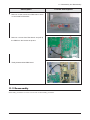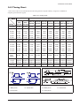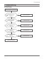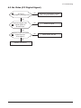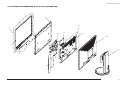
1
LCD-Monitor
Chassis LHA20BS
Model
SERVICE
LCD Monitor
203B
Manual
Fashion Feature
- Premium HAS application(Lift 80mm)
- Magic Rotation application
(Auto pivot Delete)
- Embeded Power, Mechanical S/W
application
Copyright
Trademarks
©2005 by Samsung Electronics Co., Ltd.
Samsung is the registered trademark of Samsung
Electronics Co., Ltd.
All rights reserved.
This manual may not, in whole or in part, be copied,
photocopied, reproduced, translated, or converted to
any electronic or machine readable form without prior
written permission of Samsung Electronics Co., Ltd.
LHA20BS Service Manual
First edition January 2006.
Printed in Korea.
ii
LHA20BS and MacMaster Cable Adapter are
trademarks of Samsung Electronics Co., Ltd.
Macintosh, Power Macintosh are trademarks of Apple
Computer, Inc.
All other trademarks are the property of their respective
owners.
Contents
1. Precautions ………………………………………………………………………………………………………………………………………1
1-1
1-1 Safety Precautions ……………………………………………………………………………………………………………………… 1-1
1-2 Servicing Precautions …………………………………………………………………………………………………………………… 1-2
1-3 Electrostatically Sensitive Devices (ESD) Precautions ……………………………………………………………………………… 1-2
1-4 Installation Precautions ………………………………………………………………………………………………………………… 1-3
2. Product specifications …………………………………………………………………………………………………………………………2
2-1
2-1 Fashion Feature…………………………………………………………………………………………………………………………… 2-1
2-2 Specifications ……………………………………………………………………………………………………………………………… 2-1
2-3 LS20BRD feature ………………………………………………………………………………………………………………………… 2-2
2-4 Spec Comparison ………………………………………………………………………………………………………………………… 2-3
2-5 Option Specification ……………………………………………………………………………………………………………………… 2-4
3. Alignments and Adjustments …………………………………………………………………………………………………………………3
3-1
3-1 Required Equipment
…………………………………………………………………………………………………………………… 3-1
3-2 Automatic Color Adjustment …………………………………………………………………………………………………………… 3-1
3-3 DDC EDID Data Input …………………………………………………………………………………………………………………… 3-1
3-4 Service Function Spec.
………………………………………………………………………………………………………………… 3-2
3-5 Hidden Key list …………………………………………………………………………………………………………………………… 3-3
3-6 EDID Installation with Windows Program ………………………………………………………………………………………………3-4
3-7 Execution Items after replacing the main board ………………………………………………………………………………………3-4
4-1
4. Troubleshooting …………………………………………………………………………………………………………………………………4
4-1 No Power ……………………………………………………………………………………………………………………………………4-1
4-2 No Video (PC Analog Signal) …………………………………………………………………………………………………………… 4-3
4-3 No Video (PC Digital Signal) …………………………………………………………………………………………………………… 4-5
5. Exploded View and Parts List
5-1
………………………………………………………………………………………………………………5
5-1 LHA20BS Exploded View
……………………………………………………………………………………………………………… 5-1
5-2 LHA20BS Parts List ……………………………………………………………………………………………………………………… 5-2
6. Electrical Parts List ……………………………………………………………………………………………………………………………6
6-1
6-1 LHA20BS Parts List ……………………………………………………………………………………………………………………… 6-1
7. Block Diagram …………………………………………………………………………………………………………………………………7
7-1
8. Wiring Diagram ……………8
8-1
Contents
9. Schematic Diagrams ……………………………………………………………………………………………………………………………9
9-1
9-1 Schematic Diagrams ……………………………………………………………………………………………………………………… 9-1
9-2 Schematic Diagrams ………………………………………………………………………………………………………………………9-3
10. Operating Instructions and Installation
……………………………………………………………………………………………………10-1
10-1 Front …………………………………………………………………………………………………………………………………… 10-1
10-2 Rear ………………………………………………………………………………………………………………………………………10-2
10-3 Using the Stand …………………………………………………………………………………………………………………………10-4
11-1
11. Disassembly and Reassembly ………………………………………………………………………………………………………………1
11-1 Disassembly …………………………………………………………………………………………………………………………… 11-1
11-2 Reassembly …………………………………………………………………………………………………………………………… 11-2
12. PCB Diagram …………………………………………………………………………………………………………………………………1
12-1
13. Circuit Descriptions ……………………………………………………………………………………………………………………………1
13-1
13-1 Block description ……………………………………………………………………………………………………………………… 13-1
13-2 Block operating
……………………………………………………………………………………………………………………… 13-2
14. Reference Infomation ……………………………………………………………………………………………………………………… 14-1
14-1 Technical Terms ……………………………………………………………………………………………………………………… 14-1
14-2 Pin Assignments …………………………………………………………………………………………………………………………14-4
14-3 Timing Chart ……………………………………………………………………………………………………………………………14-5
14-4 Preset Timing Modes ………………………………………………………………………………………………………………… 14-6
14-5 Panel Description ……………………………………………………………………………………………………………………… 14-7
-This Service Manual is a property of Samsung
Electronics Co., Ltd.
Any unauthorized use of Manual can be punished
under applicable International and/or domestic
law.
Samsung Electronics Co.,Ltd.
416, Maetan-3Dong, Yeongtong-Gu, Suwon City,
Gyeonggi-Do, Korea, 443-742
Printed in Korea
P/N : BN82-00136F-00
URL : http://itself.sec.samsung.co.kr/
10 Operating Instructions and Installation
10 Operating Instructions and Installation
10-1 Front
1. Menu button
Opens the OSD menu. Also use to exit the OSD
menu or return to the previous menu.
3) Internet : Medium brightness
For working with a mixture of images such as text
and graphics.
2. MagicBright button
MagicBright is a new feature providing optimum
viewing environment depending on the contents of
the image you are watching. Currently six different
modes are available: Custom, Text, Internet,
Game, Sport and Movie. Each mode has its own
pre-configured brightness value. You can easily
select one of six settings by simply pressing
MagicBright control buttons.
4) Game
For watching motion pictures such as a game.
1) Custom
Although the values are carefully chosen by our
engineers, the pre-configured values may not be
comfortable to your eyes depending on your taste.
If this is the case, adjust the brightness and contrast by using the OSD menu.
3. Bright button
When OSD is not on the screen, push the button
to adjust brightness.
5) Sport
For watching motion pictures such as a sport.
6) Movie : High brightness
For watching motion pictures such as a DVD or
Video CD.
2,3. Adjust buttons
Adjust items in the menu.
2) Text : Normal brightness
For documentations or works involving heavy text.
10-1
10 Operating Instructions and Installation
4. Enter button / Source button
Activates a highlighted menu item. /
Push the 'SOURCE', then selects the video signal
while the OSD is off. (When the source button is
pressed to change the input mode, a message
appears in the left upper side of the screen
displaying the current mode -- analog or digital
input signal.)
Note : If you select the digital mode, you must connect your monitor to the graphic card's port using
the DVI cable.
5. Auto button
When the 'AUTO' button is pressed, the Auto
Adjustment screen appears as shown in the animated screen on the center. Auto adjustment
allows the monitor to self-adjust to the incoming
video signal. The values of fine, coarse and position are adjusted automatically. (Available in analog mode only)
6. Power button
Use this button for turn the monitor on and off.
10-2 Rear
(The configuration at the back of the monitor may vary from product to product.)
1. POWER S/W : Switch the monitor on and off.
2. POWER IN : Power cord, plugs into monitor and wall
receptacle.
10-2
10 Operating Instructions and Installation
DVI IN port : Connect the DVI Cable to the DVI IN port
on the back of your monitor.
(SOURCE : digital)
RGB IN port : Connect the signal cable to the RGB IN
port on the back of your monitor.
(SOURCE : analog)
Kensington Lock : The Kensington lock is a device
used to physically fix the system
when using it in a public place.
(The locking device has to be
purchased separately.)
Stand Stopper : Remve the fixing pin on the stand to lift
the monitor up and down.
10-3
10 Operating Instructions and Installation
10-3 Using the Stand
10-3-1 Removing the base
1. Turn off your monitor and unplug its power cord.
2. Lay the LCD monitor face-down on a flat surface with a cushion beneath it to protect the screen.
3. Remove four screws(A) and then remove the Stand from the LCD monitor.
10-4
10 Operating Instructions and Installation
10-3-2 Attaching a Base
- This monitor accepts a 100mm x 100mm VESA-compliant mounting interface pad.
1
2
3
4
A. Monitor
B. Mounting interface pad
1. Turn off your monitor and unplug its power cord.
2. Lay the LCD monitor face-down on a flat surface with a cushion beneath it to protect the screen.
3. Remove four screws and then remove the stand from the LCD monitor.
4. Align the mounting interface Pad with the holes in the rear cover mounting pad and secure it with four
screws that came with the arm-type base, wall mount hanger or other base.
10-5
10 Operating Instructions and Installation
Memo
10-6
11 Disassembly and Reassembly
11 Disassembly and Reassembly
This section of the service manual describes the disassembly and reassembly procedures for the 203B TFT-LCD monitors.
WARNING: This monitor contains electrostatically sensitive devices. Use caution when handling
these components.
11-1 Disassembly
Cautions:
1.Please the power off, before disassemble the monitor.
2.Please do not use other jig except given jig when disassemble.
3.Please disassemble based on given process as below.
4.Back cover open JIG : BH81-00001A
Description
Picture Description
1. The monitor puts on the cushion and
remove two screws on VESA cover.
2. Pull up the VESA cover and remove it.
11-1
11 Disassembly and Reassembly
Description
3. Remove 1 screws from Lamp shield
4. Disconnect a FUNCTION Wire
from PCB ASSY.
5. Disconnect 4 Lamp Wire and Wire.
6. Disconnect a LVDS Wire from Panel.
11-2
Picture Description
11 Disassembly and Reassembly
Description
Picture Description
7. Remove 4 hexa screws from PBA board which
is connected PCB bracket.
8. Remove 4 screws from PBA board and pull up
the PBA from the bracket as picture.
9. Totally disassembled PBA board.
11-2 Reassembly
Reassembly procedures are in the reverse order of disassembly procedures.
11-3
11 Disassembly and Reassembly
Memo
11-4
13 Circuit Descriptions
13 Circuit Descriptions
13-1 Block description
13-1
13 Circuit Descriptions
13-2 Block operating
No
Feature
1
Scaler
2
DDR
MEMORY
3
MICOM
Description
Scaler Integrate ADC and TMDS, Scaling part.
DDR memory Save frame information that SCALER needed .
Microcontroller.
Micom control all function of monitor.
Analog signal from the PC is changed to digital signal using the A/D converter integrated in scaler(MST6281).
Scaler scale this digital singal to optimal signal fit to the panel and encode the LVDS signal.
This LVDS signla enter the panel to show the image through the LVDS Connector.
In Case of DVI singal, integrated TMDS Block is operating and processing.
MIcom control the all function of the monitor and OSD.
DC/DC Block make a suitable voltages from output 14V of I/P board which are used for function of all
devices such as scaler, micom, memory, panel
IP board supplies voltages for main board and panel, at the same time, controls the lamp of panel back light.
13-2
14 Reference Infomation
14 Reference Infomation
14-1 Technical Terms
- TFT-LCD
(Thin film Transistor Liquid Crystal Display)
ADC(Analog to Digital Converter)
This is a circuit that converts from analog signal to
digital signals.
- PLL(Phase Locked Loop)
During progressing ADC, Device makes clock
synchronizing HSYNC with Video clock
- Inverter
Device that supplies Power to LCD panel lamp.
This device generates about 1,500~2,000V.
- SMPS(Switching Mode Power Supply)
Switching Mode Power supply. This design
technology is used to step up/down the input
power by switching on/off
- FRC(Frame Rate Controller)
Technology that change image frame quantity
displayed on screen for one second.
Actually TFT-LCD panel require 60 pcs of frame
for one second.
so,this technology is needed to convert input
image to 60 pcs regardless input frame quantity.
- Image Scaler
Technology that convert various input resolution to
other resolution.(ex. 640* 480 to 1024*768)
- Auto Configuration(Auto adjustment)
This is an algorithm to adjust monitor to optimum
condition by pushing one key.
- OSD(On Screen Display)
On screen display. customer can control the
screen easily with this.
- Image Lock
This means "Fineness adjustment" in LCD
Monitor, the features are "Fine" and "Coarse"
- FINE
"Fine" adjustment is used to adjust visibility by
control phase difference.
- COARSE
This is a adjustment by tuning with Video colck
and PLL clock.
- DVI (Digital Visual Interface)
This provides a high speed digital connection for
visual data types that is display technology
independent. this interface is primarily forcused at
providing a connection between a computer and
its display device.
- L.V.D.S.(Low Voltage Differential Signaling)
a kind of transmission method for Digital.
It can be used from Main PBA to Panel.
- DVI (Digital Visual Interface)
This provides a high speed digital connection for
visual data types that is display technology
independent. this interface is primarily forcused at
providing a connection between a computer and its
display device.
- T.M.D.S
(Transition minimized Differential Signaling)
a kind of transmission method for Digital.
It can be used from Video card to Main PBA.
- DDC(Display data channel)
It is a communication method between Host
Computer and related equipment.
It can make it Plug and Play between PC and
Monitor.
- EDID
Extended Display Identification Data PC can
recognize the monitor information as Product data,
Product name,Display mode,Serial number and
Signal source,etc through DDC Line communicating
with PC and Monitor.
14-1
14 Reference Infomation
- Dot Pitch
The image on a monitor is composed of red, green
and blue dots. The closer the dots, the higher the
resolution. The distance between two dots of the
same color is called the 'Dot Pitch'. Unit: mm
- Vertical Frequency
The screen must be redrawn several times per
second in order to create and display an image for
the user. The frequency of this repetition per
second is called Vertical Frequency or Refresh
Rate. Unit: Hz
Example: If the same light repeats itself 60 times
per second, this is regarded as 60 Hz.
- Horizontal Frequency
The time to scan one line connecting the right
edge to the left edge of the screen horizontally is
called Horizontal Cycle. The inverse number of the
Horizontal Cycle is called Horizontal Frequency.
Unit: kHz
- Interlace and Non-Interlace Methods
Showing the horizontal lines of the screen from the
top to the bottom in order is called the
Non-Interlace method while showing odd lines and
then even lines in turn is called the Interlace
method. The Non-Interlace method is used for the
majority of monitors to ensure a clear image. The
Interlace method is the same as that used in TVs.
- Plug & Play
This is a function that provides the best quality
screen for the user by allowing the computer and
the monitor to exchange information automatically.
This monitor follows the international standard
VESA DDC for the Plug & Play function.
- Resolution
The number of horizontal and vertical dots used to
compose the screen image is called 'resolution'.
This number shows the accuracy of the display.
High resolution is good for performing multiple
tasks as more image information can be shown on
the screen.
Example: If the resolution is 1280 x 1024 , this
means the screen is composed of 1280 horizontal
dots (horizontal resolution) and 1024 vertical lines
(vertical resolution).
- S-Video
Short for "Super Video." S-Video allows up to 800 lines
of horizontal resolution, enabling high-quality video.
14-2
- External Device Input
External device input refers to video input from
such external video devices as VCRs, camcorders
and DVD players, separate from a TV broadcast.
- DVD
A type of digital disk technology that takes up only
the benefits of CD and LD, to implement a high
resolution/quality, which enables the user to enjoy
clearer images.
14 Reference Infomation
- Connecting the Monitor
1.
Connect the DC adapter for your monitor to the power port on the back of the monitor.
Plug the power cord for the monitor into a nearby outlet.
2-1. Using the D-sub (Analog) connector on the video card.
Connect the signal cable to the 15-pin, D-sub connector on the back of your monitor.
2-2. Using the DVI (Digital) connector on the video card.
Connect the DVI cable to the DVI port on the back of your monitor.
2-3. Connected to a Macintosh.
Connect the monitor to the Macintosh computer using the D-SUB connection cable.
2-4. In the case of an old model Macintosh, you need to connect the monitor using a special Mac adapter.
3. Turn on your computer and monitor. If your monitor displays an image, installation is complete.
- You may get a blank screen depending on the type of video card you are using, if you connect
simultaneously both the D-Sub and DVI cables to one computer.
- If you properly connect your monitor using the DVI connector but get a blank screen, check to see if
the monitor status is set to analog. Press power button to have the monitor double-check the input
signal source.
14-3
14 Reference Infomation
14-2 Pin Assignments
Sync
Type
Pin No.
1
2
3
4
5
6
7
8
9
10
11
12
13
14
15
15-Pin D-Sub Signal Cable Connector
Separate
Composite
Sync-on-green
Red
Green
Blue
GND
DDC Return (GND)
GND-R
GND-G
GND-B
DDC Power Input (+5V)
Self Raster
GND
Bi-Dr Data (SDA)
H-Sync.
V-Sync.
DDC Clock (SCL)
Red
Green
Blue
GND
DDC Return (GND)
GND-R
GND-G
GND-B
DDC Power Input (+5V)
Self Raster
GND
Bi-Dr Data (SDA)
H/V-Sync.
Not Used
DDC Clock (SCL)
Red
Green + H/V Sync.
Blue
GND
DDC Return (GND)
GND-R
GND-G
GND-B
DDC Power Input (+5V)
Self Raster
GND
Bi-Dr Data (SDA)
Not Used
Not Used
DDC Clock (SCL)
Sync
Type
Pin No.
14-4
24P DVI-D
1
Rx2-
13
No Connection
2
Rx2+
14
+5V_M
3
GND
15
Self Raster
4
No Connection
16
+5V_M
5
No Connection
17
Rx0-
6
DDC Clock (SCL)
18
Rx0+
7
DDC Data (SDA)
19
NC
8
NC
20
No Connection
9
Rx1-
21
No Connection
10
Rx1+
22
NC
11
NC
23
RxC+
12
No Connection
24
RxC-
14 Reference Infomation
14-3 Timing Chart
- This section of the service manual describes the timing that the computer industry recognizes as standard for
computer-generated video signals.
Table 14-1 Timing Chart
VESA
IBM
Mode
VGA2/
70 Hz
Timing
VGA3/
60 Hz
640/75 Hz 800/60 Hz 800/75 Hz 1024/60 Hz 1024/75 Hz 1280/60 Hz 1280/75 Hz
720 x 400 640 x 480
640x480
800x600
800x600
1024x768 1024x768 1280x1024 1280x1024
fH (kHz)
31.469
31.469
37.500
37.879
46.875
48.363
60.023
63.981
79.975
A μsec
31.777
31.778
26.667
26.400
21.333
20.677
16.660
11.852
12.504
B μsec
3.813
3.813
2.032
3.200
1.616
2.092
1.219
1.037
1.067
C μsec
1.589
1.589
3.810
2.200
3.232
2.462
2.235
2.296
1.837
D μsec
26.058
26.058
20.317
20.000
16.162
15.754
13.003
9.259
9.481
E μsec
0.318
0.318
0.508
0.000
0.323
0.369
0.203
0.000
0.119
fV (Hz)
70.087
59.940
75.000
60.317
75.000
60.004
75.029
60.020
75.025
O msec
14.268
16.683
13.333
16.579
13.333
16.666
13.328
16.005
13.329
P msec
0.064
0.064
0.080
0.106
0.064
0.124
0.050
0.047
0.038
Q msec
0.858
0.794
0.427
0.607
0.448
0.600
0.466
0.594
0.475
R msec
13.155
15.761
12.800
15.840
12.800
15.880
12.795
15.630
12.804
S msec
0.191
0.064
0.027
0.0261
0.021
0.062
0.017
0.016
0.013
28.322
26.175
31.500
40.000
49.500
75.000
78.750
108.000
Clock
Freq.
(MHz)
135.000
Polarity
H.Sync
Negative Negative Negative Positive
Positive Negative
Positive
Positive
Positive
V.Sync
Positive Negative Negative Positive
Positive Negative
Positive
Positive
Positive
Remark
Separate Separate Separate Separate Separate Separate Separate Separate Separate
H/V Composite Sync
Separate Sync
Video
Video
C
D
E
Q
R
S
Sync-on-Green
Sync
Sync
B
P
A
O
A : Line time total
B : Horizontal sync width
O : Frame time total
P : Vertical sync width
C : Back porch
D : Active time
Q : Back porch
R : Active time
E : Front porch
S : Front porch
14-5
14 Reference Infomation
14-4 Preset Timing Modes
- If the signal transferred from the computer is the same as the following Preset Timing Modes, the screen
will be adjusted automatically. However, if the signal differs, the screen may go blank while the power LED
is on. Refer to the video card manual and adjust the screen as follows.
Table 1. Preset Timing
Display Mode
Horizontal
Frequency
(kHz)
Vertical Frequency
(Hz)
Pixel Clock
(MHz)
Sync Polarity
(H/V)
MAC, 640 x 480
35.000
66.667
30.240
-/-
MAC, 832 x 624
49.726
74.551
57.284
-/-
IBM, 640 x 350
31.469
70.086
25.175
+/-
IBM, 640 x 480
31.469
59.940
25.175
-/-
IBM, 720 x 400
31.469
70.087
28.322
-/+
VESA, 640 x 480
37.500
75.000
31.500
-/-
VESA, 640 x 480
37.861
72.809
31.500
-/-
VESA, 800 x 600
35.156
56.250
36.000
+,-/+,-
VESA, 800 x 600
37.879
60.317
40.000
+/+
VESA, 800 x 600
46.875
75.000
49.500
+/+
VESA, 800 x 600
48.077
72.188
50.000
+/+
VESA, 1024 x 768
48.363
60.004
65.000
-/-
VESA, 1024 x 768
56.476
70.069
75.000
-/-
VESA, 1024 x 768
60.023
75.029
78.750
+/+
VESA, 1280 x 1024
63.981
60.020
108.00
+/+
VESA, 1280 x 1024
79,976
75,025
135,00
+/+
VESA, 1600 x 1200
75.000
60.000
162.00
+/+
Horizontal Frequency
The time to scan one line connecting the right edge to the left edge of the screen horizontally is called
Horizontal Cycle and the inverse number of the Horizontal Cycle is called Horizontal Frequency. Unit: kHz
Vertical Frequency
Like a fluorescent lamp, the screen has to repeat the same image many times per second to display an
image to the user. The frequency of this repetition is called Vertical Frequency or Refresh Rate. Unit: Hz
14-6
14 Reference Infomation
14-5 Panel Description
Maker
SEC
SEC
SEC
SEC
SEC
SEC
SEC
SEC
SEC
SEC
SEC
SEC
SEC
SEC
SEC
SEC
SEC
SEC
SEC
SEC
SEC
SEC
SEC
SEC
SEC
SEC
SEC
SEC
SEC
SEC
SEC
SEC
SEC
SEC
SEC
SEC
SEC
SEC
SEC
SEC
SEC
SEC
SEC
SEC
SEC
SEC
SEC
SEC
SEC
SEC
SEC
SEC
SEC
SEC
SEC
SEC
SEC
SEC
SEC
SEC
SEC
SEC
SEC
SEC
SEC
SEC
SEC
SEC
SEC
SEC
SEC
SEC
SEC
SEC
SEC
SEC
SEC
VENDOR P/N
LT140X1-002
LT150XS-L01
LT150XS-L01-B
LTM150XS-L02
LT181E2-132
LT150XS-T01
LTM181E3-132
LT170E2-131
LT181E2-131
LTM170E4-L01
LTM240W1-L01
LTM213U3-L01
LTM150XH-L01
LTM150XH-L03
LTM150XS-L01
LTM181E4-L01
LTM170EH-L01
LTM170E5-L01
LTM150XH-L11
LTM213U4-L01
LTM150XH-L01(ZPD)
LTM150XH-L04
LTM170W1-L01
LTM150XH-L06
LTM153W1-L01
LTM170EH-L05
LTM170E5-L03
LTM190E1-L01
LTM181E5-L01
LTM150XP-L01
LTM240W1-L02
LTM170EU-L01
LTM170E5-L04
LTA220W1-L01
LTM170E6-L02
LTM170W1-L01
LTM170EH-L01
LTM170E5-L01
LTM170EH-L05
LTM170E5-L03
LTM170EU-L01
LTM170E5-L04
LTM170E6-L02
LTM150XH-L06
LTM153W1-L01
LTM170W1-L01
LTM170EH-L05
LTA400W1-L01
LTM153W1-L01
LTM150XH-L06
LTM170W1-L01
LTM170EH-L05
LTM220W1-L01
LTM150XH-L06
LTM153W1-L01
LTM170WP-L01
LTM213U4-L01
LTA260W1-L01
LTA220W1-L01
LTA320W1-L01
LTM213U4-L01
LTM170E6-L04
LTM190E1-L01
M150X4-L06
LTA170V1
LTM190E1-L02
LTM170EX-L01
LTM170E8-L01
LTM170E6-L04
LTA320W1-L02
LTM190E1-L03
LTM240W1-L03
LTM190E1-L02
LTM190E4-L01
LTM170E8-L01
LTM170EX-L01
LTM190E1-L03
PANEL_CODE
BN07-00004A
BN07-00009A
BN07-00022A
BN07-00005A
BN07-00001A
BN07-00010A
BN07-00019A
BN07-10001D
BN07-10001E
BN07-00018A
BN07-00015A
BN07-00016A
BN07-00026A
BN07-00027A
BN07-00032A
BN07-00034A
BN07-00036A
BN07-00037A
BN07-00041A
BN07-00039A
BN07-00045A
BN07-00046A
BN07-00047A
BN07-00053A
BN07-00054A
BN07-00055A
BN07-00056A
BN07-00057A
BN07-00061A
BN07-00065A
BN07-00062A
BN07-00071A
BN07-00072A
BN07-00074A
BN07-00075A
BN07-00082A
BN07-00080A
BN07-00081A
BN07-00083A
BN07-00084A
BN07-00085A
BN07-00086A
BN07-00087A
BN07-00091A
BN07-00092A
BN07-00100A
BN07-00097A
BN07-00109A
BN07-00110A
BN07-00111A
BN07-00112A
BN07-00113A
BN07-00114A
BN07-00117A
BN07-00118A
BN07-00119A
BN07-00039A
BN07-00121A
BN07-00074B
BN07-00108A
BN07-00124A
BN07-00129A
BN07-00088A
BN07-00137A
BN07-00139A
BN07-00128A
BN07-00143A
BN07-00144A
BN07-00129B
BN07-00108B
BN07-00151A
BN07-00134A
BN07-00128B
BN07-00145A
BN07-00158A
BN07-00159A
BN07-00151B
PANEL_ABB
SA
SB
SC
SD
SE
SF
SG
SH
SJ
SK
SL
SM
SN
SP
SQ
SR
SS
SU
SV
SW
SX
SY
SZ
EA
EB
EC
ED
EE
EF
EG
EH
EJ
EK
EL
EM
EN
EP
EQ
ER
ES
ET
EU
EV
EW
EX
EY
EZ
S1
S2
S3
S4
S5
S6
S7
S8
S9
E1
E2
E3
E4
E5
E6
E7
E8
E9
E10
E11
E12
E13
E14
E15
E16
E17
E18
E19
E20
E21
STICKER_CODE
BN68-00239H
Remarks
DELL(ZPD)
PVA
TN
PVA
PVA
ZPD
New panel with high brightness
Panel for TV
Panel for TV/ High luminance for 450cd _ SONY&EOS Team Panel for TV
Use NIKE MODEL
Panel EOS proj. for high brightness of 17" EH-L05
Dell 1702FP pro. E4. EH mechanical Compatible
DELL 1900 FP
18" narrow bezel GH18PS
AMLCD PVA PANEL
Panel for 15" Wide TV
Slim design, TN
E5-L04 6 bits FRC... for IBM
Panel for 22" TV
AMLCD Narrow & slim design 17" PVA mode
LTM170W1-L01 ZPD panel
LTM170EH-L01 ZPD panel
LTM170E5-L01 ZPD panel
LTM170EH-L05 ZPD panel
LTM170E5-L03 ZPD panel
LTM170EU-L01 ZPD panel
LTM170E5-L04 ZPD panel
LTM170E6-L02 ZPD panel
Color coordinates change for LCD TV
AMLCD WIDE 15",9/10
Color Coordinates change code management
LTM170E5-L05 Color Coordinates Change Panel Code
PANEL of AMLCD 40" TV
Color coordinates change 0.280/0.290, 10000k & ZPD Panel
Color coordinates change 0.280/0.290, 10000k & ZPD Panel
Color coordinates change 0.280/0.290, 10000k & ZPD Panel
Color coordinates change 0.280/0.290, 10000k & ZPD Panel
ZPD Panel for AMLCD 22" TV
ZPD Panel code
ZPD Panel code
PVA Panel for NIKE
21.3" NARROW
VENUS
"Panel B-level panel code for 22"" TV Panel "
"Panel for AMLCD 32"" TV"
NARROW BEZEL 21 " PANEL
"HIGHLAND 17"" LOW PANEL (Panel only for TCO03)"
LTM190E1-L01 ZPD panel
15" Narrow & Slim panel
"17"" Panel for Muse 4:3 VGA TV"
"New Panel from AMLCDl, Specification : 6bit Driver IC"
"Development new Panel from AMLCD"
"Development new Panel from AMLCD"
"ZPD panel for AMLCD (Panel only for TCO03)"
"Creat B-level Panel code for AMLCD 32"" TV"
"Development new 19"" Panel form AMLCD (Panel only for TCO03)"
"AMLCD 24"" panel development"
"New Panel from AMLCD, Specification : 6bit Driver IC(ZPD)"
"AMLCD 24"" new panel development"
"ZPD code derivation"
"ZPD code derivation"
"Creat new panel code for AMLCD 19"" (Panel only for TCO03)"
14-7
14 Reference Infomation
Maker
SEC
SEC
SEC
SEC
SEC
SEC
SEC
SEC
SEC
SEC
SEC
SEC
SEC
SEC
SEC
SEC
SEC
SEC
SEC
SEC
SEC
SEC
SEC
SEC
SEC
SEC
SEC
SEC
SEC
SEC
SEC
SEC
SEC
SEC
SEC
SEC
SEC
SEC
SEC
CPT
CPT
CPT
CPT
CPT
CPT
CPT
CPT
CPT
CPT
CPT
CPT
TOSHIBA
TOSHIBA
TOSHIBA
TOSHIBA
TOSHIBA
TOSHIBA
TOSHIBA
TOSHIBA
HANNSTAR
HANNSTAR
HANNSTAR
HANNSTAR
HANNSTAR
HANNSTAR
TORISAN
TORISAN
TORISAN
TORISAN
TORISAN
TORISAN
TORISAN
TORISAN
TORISAN
TORISAN
TORISAN
TORISAN
14-8
VENDOR P/N
PANEL_CODE
LTA460H1-L01
LTM170EU-L11
LTM240W1-L03
LTM190E4-L01
LTM240W1-L03
LTM150XO-L01
LTM150XO-L01
LTM170EU-L11
LTA320W2-L01
LTM213U4-L01
LTM170EU-L11
LTM170EU-L11
LTM240W1-L04
LTM240W1-L04
LTM190EX-L01
LTM190EX-L02
LTA230W1-L02
LTA260W2-L01
LTM240M1-L01
LTA400W2-L01
LTM150XO-L01
LTM150XO-L01
LTM170EU-L21
LTA460W2-L03
LTM240M1-L01
M170EX-L21
LTA460H3-L01
LTM170EU-L15
LTM170E8-L21
LTM190EX-L21
LTM201U1-L01
LTM190E4-L21
LTA570H1-L01
LTM150XO-L21
LTA260W2-L11
LTA400WS-LH1
LTM213U6-L01
LTA320WS-LH2
LTA400WS-LH1
CLAA150XG09
CLAA170EA02
CLAA170EA02
CLAA150XG09
CLAA150XP01
CLAA150XP01
CLAA170EA07
CLAA170EA07
CLAA170EA07
CLAA170EA07Q
CLAA170EA07Q
CLAA150XP01F
LTM15C419(A)
LTM15C423(B)
LTM18C161
LTM15C443
LTM15C458
LTM15C458S
LTM15C458
LTM15C458S
HSD150MX41A(A)
HSD150MX12
HSD170ME13
HSD170ME13
HSD190ME12
HSD150MX17-A
TM150XG-22L03(A)
TM150XG-26L06
TM181SX-76N01
TM150XG-26L06
TM290WX-71N31
TM396WX-71N31
TM150XG-26L09
TM150XG-26L10
TM150XG-26L10
TM190SX-70N01
TM181SX-76N01
TM190SX-70N01
BN07-00157A
BN07-00160A
BN07-00134B
BN07-00145B
BN07-00134B
BN07-00164A
BN07-00164B
BN07-00160B
BN07-00172A
BN07-00124B
BN07-00189A
BN07-00189B
BN07-00188A
BN07-00188B
BN07-00191A
BN07-00191B
BN07-00184A
BN07-00185A
BN07-00195A
BN07-00186A
BN07-00197A
BN07-00197B
BN07-00202A
BN07-00187A
BN07-00195B
BN07-00206A
BN07-00200A
BN07-00214A
BN07-00218A
BN07-00222A
BN07-00190B
BN07-00223A
BN07-00196A
BN07-00229A
BN07-00239A
BN07-00245A
BN07-00231A
BN07-00244A
BN07-00245A
BN07-00141A
BN07-00148A
BN07-00148B
BN07-00141B
BN07-00173A
BN07-00173B
BN07-00174A
BN07-00174B
BN07-00174B
BN07-00220A
BN07-00220B
BN07-00236A
BN07-00002A
BN07-00006A
BN07-00008A
BN07-00031A
BN07-00043A
BN07-00077A
BN07-00078A
BN07-00099A
BN07-00020A
BN07-00030A
BN07-00180A
BN07-00180B
BN07-00210A
BN07-00226A
BN07-00021A
BN07-00042A
BN07-00048A
BN07-00059A
BN07-00063A
BN07-00064A
BN07-00073A
BN07-00089A
BN07-00090A
BN07-00098A
BN07-00106A
BN07-00107A
PANEL_ABB
E22
E23
E24
E25
E26
E27
E28
E29
SPZ
SPZ
STH
STZ
SPH
SPZ
STH
STZ
SPZ
SPZ
SPH
SPZ
STH
STZ
STZ
SPZ
SPZ
STZ
SPZ
STZ
SPZ
STZ
SPZ
SPZ
SPZ
STZ
SPZ
SPZ
SPZ
SPZ
SPZ
PA
PB
PC
PTZ
PTH
PTZ
PTH
PTZ
PTZ
PTZ
PTH
PTZ
TA
TB
TC
TD
TE
TF
TG
TH
NA
NB
NTH
NTZ
NTZ
NTZ
RA
RB
RC
RD
RE
RF
RG
RH
RJ
RK
RL
RM
STICKER_CODE
Remarks
"creat panel code for AMLCD 46"" TV "
"creat new panel code for AMLCD 17"" (Panel only for TCO03)"
"24"" panel ZPD code derivation"
"AMLCD 19"" ZPD Panel code derivation"
"24"" panel ZPD code derivation"
"AMLCD 15"" XO-L01 new panel development"
"AMLCD 15"" XO-L01 ZPD code derivation"
"AMLCD 17"" NEW panel code derivation"
AMLCD 32" NEW panel
21.3" Narrow PANEL ZPD Panel derivation
AMLCD EU-L11 Pb free panel code derivation
AMLCD EU-L11 Pb free panel ZPD code derivation
24" A-DCC new panel development
24" A-DCC panel ZPD code derivation
AMLCD 19" TN new Panel
AMLCD 19" TN new Panel ZPD derivation
AMLCD 23" 16:9 new Panel
AMLCD 26" 16:9 new Panel
24" panel with high brightness deveiopment
AMLCD 40" 16:9 new Panel
AMLCD 15" XO-L01 Pb free panel code
AMLCD 15" XO-L01 Pb free panel ZPD code
AMLCD EU-L21 ZPD new code derivation
BEETOVEN 46"ZPD new panel
24" igh brightness panel ZPD code derivation
AMLCD LTM170EX-L21 ZPD new code derivation
AMLCD 46" LED BLU panel
AMLCD EU-L15 TV high brightness ZPD new code derivation
AMLCD LTM170E8-L21 PVA ZPD new code derivation
DISPLAY LCD
AMLCD 20.1" Normal panel ZPD code derivation
HAYDN 17" PZD code PANEL derivation
AMLCD 57" new panel development
AMLCD 15" XO-L21 8ms panel code
AMLCD 26" 16:9 7Line new Panel
AMLCD 40" 16:9 SPVA 90% new Panel
AMLCD 21.3" PVA new Panel Code
AMLCD 32" 16:9 SPVA 90% new Panel
AMLCD 40" 16:9 SPVA 90% new Panel
"CPT 15"" Monitor new panel development"
"17"" CPT NEW development panel"
"17"" CPT ZPD panel code derivation"
"CPT 15"" panel ZPD code derivation (GOYA-PJT)"
CPT 15" PSWG code derivation
CPT 15" PSWG panel ZPD code
"CPT 17"" PSWG panel code derivation
CPT 17"""" PSWG type new Panel code"""
CPT 17" PSWG type new Panel code
CPT 17" PSWG R/T 8msec code derivation
CPT 17" PSWG R/T 8msec HPD code derivation
CPT 15" PSWG panel ZPD & Lead free code derivation
"TSB 15"" high brightness Panel"
Toshiba ZPD panel
TSB LTM15C458S ( ZPD )
"TTL type"
"TTL type"
Hannstar 17" TN new panel development
Hannstar 17" TN new panel development ZPD code derivation
Hannstar 19" TN new panel development
Hannstar 15" slim panel ZPD code derivation
15" XGA TN MODE(ZPD)
"RS24NS (TORISAN 29"" NEW PANEL)"
"RS24NS (TORISAN 40"" NEW PANEL)"
"Panel for 15"" TV"
"L10(change except D/IC) ZPD"
L10 NORMAL
Torisan 19" Panel
ZPD Panel code
ZPD Panel code
14 Reference Infomation
Maker
TORISAN
TORISAN
TORISAN
TORISAN
TORISAN
TORISAN
TORISAN
TORISAN
TORISAN
SHARP
SHARP
SHARP
HITACHI
HITACHI
HITACHI
HITACHI
HITACHI
HITACHI
HITACHI
IBM
UNIPAC
HYUNDAI
HYUNDAI
HYUNDAI
HYUNDAI
HYUNDAI
HYUNDAI
HYUNDAI
HYUNDAI
HYUNDAI
HYUNDAI
HYUNDAI
ACER
ACER
ACER
ACER
ACER
ACER
ACER
ACER
ACER
ACER
ACER
ACER
ACER
ACER
ACER
ACER
ACER
ACER
ACER
ACER
ACER
CHIMEI
CHIMEI
CHIMEI
CHIMEI
CHIMEI
CHIMEI
CHIMEI
CHIMEI
CHIMEI
CHIMEI
CHIMEI
CHIMEI
CHIMEI
CHIMEI
CHIMEI
CHIMEI
CHIMEI
CHIMEI
CHIMEI
CHIMEI
CHIMEI
CHIMEI
CHIMEI
NEC
VENDOR P/N
TM290WX-71N31
TM396WX-71N31
TM22OWX-71N31
TM22OWX-71N31
TM396WX-71N32A
TM190SX-70N02
TM190SX-70N02
TM150XG-A01
TM150XG-A01
LQ181E1DG11(A)
LQ150X1LW71
LQ370T3LZ41
TX38D12VC0CAA(A)
TX43DVCOCAB
TX43D15VC0CAB
TX51D11VC0CAB
TX54D11VC0CAB
TX80D12VC0CAB
TX54D11VC0CAB
ITSX94S
UM170E0
HT15X13
HT17E11-200
HT17E11-300
HT17E11-400
HT17E11-400
HT17E12
HT17E12
HT15X15-D00
HT15X15-D01
HT17E13-100
HT17E13-100
L170E3
M170EN05
M170EN05
M190EN02
M190EN02
M170EN06
T260XW01
A201SN01
M170EN06
T315XW01
M170EG01
M170EG01
M190EN04
T260XW02
M170EG01 V8
T260XW02
T315XW01
M190EN03
T315XW01
T315XW01
M201UN02 V3
M170E3-LO1
M150X3-L01
M170E4-L01
M150X2-L01
M150X3-L01
M170E3-L01
M170E4-L01
V296W1-L01
M170E6-L02
M190E2-L01
M150X4-L06
M170E6-L01
M170E6-L01
V201V1-T01
M170E6-L02
M170E6-L05
M170E6-L05
M150X4-L06
M170E5-L05
M170E5-L05
V230W1-L02
V320B1-L01
V270W1-L01
SVA150XG04TB
PANEL_CODE
BN07-00115A
BN07-00116A
BN07-00125A
BN07-00127A
BN07-00150A
BN07-00154A
BN07-00154B
BN07-00162A
BN07-00162B
BN07-10001C
BN07-00067A
BN07-00216A
BN07-00003A
BN07-00060A
BN07-00101A
BN07-00122A
BN07-00123A
BN07-00169A
BN07-00123B
BN07-00017A
BN07-00028A
BN07-00035A
BN07-00049A
BN07-00093A
BN07-00094A
BN07-00095A
BN07-00096A
BN07-00105A
BN07-00146A
BN07-00146B
BN07-00167A
BN07-00167B
BN07-00044A
BN07-00076A
BN07-00102A
BN07-00170A
BN07-00170B
BN07-00171A
BN07-00163A
BN07-00177A
BN07-00171B
BN07-00194A
BN07-00192A
BN07-00192B
BN07-00203A
BN07-00208A
BN07-00221A
BN07-00233A
BN07-00234A
BN07-00224A
BN07-00237A
BN07-00238A
BN07-00168A
BN07-00050A
BN07-00051A
BN07-00052A
BN07-00066A
BN07-00079A
BN07-00103A
BN07-00104A
BN07-00120A
BN07-00126A
BN07-00131A
BN07-00137A
BN07-00133A
BN07-00133B
BN07-00135A
BN07-00126B
BN07-00152A
BN07-00152B
BN07-00137B
BN07-00165A
BN07-00165B
BN07-00209A
BN07-00207A
BN07-00136A
BN07-00225A
PANEL_ABB
RN
RP,Q
RR
RS
RT
RMH
RMZ
RTH
RTZ
PA
PB
FAZ
HA
HB
HC
HD
HE
HIZ
HIZ
IA
UA
DA
DB
DC
DD
DE
DF
DG
DH
DJ
DTH
DTZ
AA
AB
AC
AMH
AMZ
ATH
AMZ
ATZ
ATZ
AMZ
ATH
ATZ
ATH
AMZ
ATZ
AMZ
AMZ
AMZ
AMZ
AMZ
AMZ
CA
CB
CC
CD
CE
CF
CG
CH
CJ
CK
CL
CM
CN
CP
CQ
CR
CS
CT
CTH
CTZ
CMZ
CMZ
CMZ
BTZ
STICKER_CODE
Remarks
"Color Coordinates change panel for TORISAN 29"" TV"
"Color Coordinates change panel for TORISAN 40"" TV"
"Development TORISAN 22"" TV PANEL (ZPD)"
"Development TORISAN 22"" TV PANEL (HPD)"
120V inverter Exclusive panel
Torisan 6bit panel code Derivation
Torisan 6bit panel code Derivation
Torisan 15" Narrow & Slim panel development
Torisan 15" N&S panel ZPD code Derivation
SHARP 15" PVA PANEL
Rome2
17" SXGA PVA MODE
ZPD Panel
20.1" NARROW
21.3" NARROW
"Development new panel for Hitachi 32"" TV (ZPD)"
Hitachi 21.3"ZPD panel
Loaded by cisdba
TN MODE
HT17E11-300 ZPD panel
HT17E11-400 normal panel
HT17E11-400 ZPD panel code
HT17E12 ( Narow & slim Design )
ZPD Panel code
"Development for Ares 15"" Hydis TV"
"Derivation panel HPD for Ares 15"" Hydis TV "
"PINEHURST-2(IBM) PJT 17"" HYDIS PANEL Derivation"
"PINEHURST-2(IBM) Hydis 17"" ZPD code Derivation"
TN(ADT)
AU 17" Panel ( Narrow & slim design )
ZPD Panel code
"AU Monitor 19"" new panel development (P19-1S)"
"AU 19"" ZPD code derivation (ZPD)"
"AU Monitor 17"" New panel development "
"AU 26"" new panel development (NF26EO)"
"AU TV panel 20.1"" TN SVGA new panel development"
AU Monitor 17" ZPD code derivation
AU 32" new
AU TN PSWG type new Panel code
AU TN PSWG type NEW panel code derivation
AU Monitor 19" ZPD new Panel code
AUO 26" ZPD panel
AU TN PSWG type new Panel (8msec) ZPD code derivation
AUO 26" Panel new (Cosmetic spec down grade)
AUO 32" Grade new (Cosmetic spec down grade)
AU Monitor 19" MVA new code derivation
LCD TV VE project new
LCD TV VE project new
TN PANEL
COMPATIBLE
MVA PANEL
CHIME 15"I PVA PANEL
Chimei ZPD panel
ZPD Panel code
ZPD Panel code
MVA
HIGHLAND 17" LOW PANEL
GH19AS,BS CHIMEI PANEL
15" Narrow & Slim panel
"2003-03-11 vendor change"
ZPD derivation panel
CHIMEI 20.1" panel development
"HIGHLAND 17"" LOW PANEL ZPD derivation panel"
"CMO 17"" new panel development code"
"CMO 17"" ZPD panel code derivation"
Chimei 15" Narrow & Slim panel ZPD derivation
CMO 17" new panel development code (GOYA2-PJT)
CMO 17" ZPD panel(GOYA2-PJT)
CMO 23" development
CMO 32" development
CHI MEI 27" panel development
SVA NEC 15" panel ZPD code
14-9
14 Reference Infomation
Memo
14-10
2 Product Specifications
2 Product Specifications
2-1 Fashion Feature
-. Premium HAS application(Lift 80mm)
-. Magic Rotation application(Auto pivot Delete)
-. Embeded Power, Mechanical S/W application
2-2 Specifications
Item
Description
LCD Panel
TFT-LCD panel, RGB vertical stripe, normally black transmissive,
20-Inch viewable, 0.255 (H) x 0.255 (V) mm pixel pitch
Scanning Frequency
Horizontal : 31 kHz ~ 80 kHz (Automatic)
Vertical : 56 Hz ~ 75 Hz (UXGA : 60 Hz)
Display Colors
16.7 Million colors
Maximum Resolution
Horizontal : 1600 Pixels
Vertical : 1200 Pixels
Input Signal
Analog / Digital
Input Sync Signal
Seperate H/V sync, Composite H/V, Sync-on-Green, Automatic synchroniza
tion whitout external swith of sync type
Level : TTL level
Maximum Pixel Clock rate
162 MHz (Analog/Display)
Active Display
Horizontal/Vertical
408(H) x 306(W)
AC power voltage & Frequency
AC 100 ~ 240 Volts, 60/50 Hz ± 3 Hz
Power Consumption
50W (Analog/Display)
Dimensions
Set (W x D x H) - Normal
- Pivot
HEAD ONLY(W x D x H)
HEIGHT ADJUSTABE RANGE
PIVOT ANGLE
SWIVEL ANGLE
TILT ANGLE
Package
Weight (Set/Package)
444.0 x 200.0 x 427.6 mm(17.5 x 7.9 x 16.8 inch)
344.0 x 200.0 x 472.6 mm
444.0 x 74.50 x 344.0 mm
80 mm (IN NORMAL STATE ONLY!)
90 degree
0 ~ 350 degree
-4 ~ 18 degree
424.0 x 235.0 x 551.0 mm (16.7 x 9.3 x 21.7 inch)
7.7 kg / 9.0 kg
Environmental Considerations
Operating Temperature : 50° F ~ 104° F (10° C ~ 40° C)
Operating Humidity : 10% ~ 80%
Storage temperature : -4° F ~113 ° F (-20° C ~ 45° C)
Storage Humidity : 5% ~ 90%
- Designs and specifications are subject to change without prior notice.
2-1
2 Product Specifications
2-3 LS20BRD feature
No
Feature
1
Auto Auto
2
Auto Power
on/off
204B can check the change of Source
Automatically and change the source to the active Input
3
Wall mount
204B supports Wall mount(100 X 100)
4
Gamma &
Color
temperature
Adjust
204B supports 3 step Adjustment
for Gamma & Color temperature
5
Magic Bright
204B supports 6 different brightness mode
(Text/Internet/game/sport/Movie/Custom)
6
Sharpness
2-2
Feature
If 204B turns on in some resolution for the first time, it can execute
Auto adjustment automatically for the high Quality
Adjust the Sharpness
Operating method
2 Product Specifications
2-4 Spec Comparison
Model
-)"#4
#
-4#3%
#
Design
4DSFFO4J[F
#SJHIUOFTT
DE̅
DE̅
$POUSBTU
'BTU3FTQPOTF
5JNF
NT
5ms
.BHJD1JWPU
0
8IFO.POJUPSJTSPUBUFEBT1JWPU
TFOTPSJTBQQMJFEUP1#"4DSFFOJT
DIBOHFEBVUPNBUJDBMMZ
X
.BHJD5VOF
7FS
7FS
4IBSQOFTT
0
O
TUFQT
5FYU*OUFSOFU4QPSUT.PWJF
(BNF$VTUPN
TUFQT
5FYU*OUFSOFU4QPSUT.PWJF
(BNF$VTUPN
.BHJD#SJHIU
2-3
2 Product Specifications
2-5 Option Specification
Item
Item Name
CODE.NO
Quick Setup Guide
BN68-00376L
Warranty Card
(Not available in all locations)
2-4
Remark
BH68-00261F
User's Guide,
Monitor Driver,
MagicTuneŞ software
BN59-00480H
D-Sub(15 Pin)
Cable
BN39-00244B
Power Cord
3903-000085
DVI Cable
BN39-00246F
Sold separately
4 Troubleshooting
4 Troubleshooting
4-1 No Power
There is no light in the power indicator.
1
Does proper DC 14 V
appear at Pin 5,6,7
of CN101?
No
Check the IP Board.
Yes
2
Does proper DC 5V
appear at Output of
IC203?
No
Check the IC 203
Yes
3
Does proper DC 3.3V
appear at
Pin 4 of the IC403?
No
Check the IC 403.
Yes
4
Does proper DC 2.5V
appear at
Pin 3 of the IC301?
No
Check the IC 301.
Yes
5
Does proper DC 1.8V
appear at
Pin 2 of the IC304?
No
Check the IC 304.
Yes
Check IC201 and IC302.
4-1
4 Troubleshooting
WAVEFORMS
1
2
3
4
5
4-2
4 Troubleshooting
4-2 No Video (PC Analog Signal)
6
Is pin9 of
CN501(BKLT_EN)high(3.3V)?
No
Check TFT_LCD panel or inverter
and connection between then.
Yes
Does the analog video signal
7 appear at R101,105, 108
(Red,Green,Blue)?
No
Check pc signal.
Yes
8
Does the X201 and X200
oscilate Properly?
No
Check the X200, IC201.
Yes
Does the proper clock pules
appear at Pin6,7 of
the CN201?
10
No
Check IC302 and IC201.
Yes
Replace LCD Panel.
4-3
4 Troubleshooting
WAVEFORMS
6
7
8
10
4-4
4 Troubleshooting
4-3 No Video (PC Digital Signal)
1
Is Pin9 of
CN501(BKLT_EN)high(3.3V)?
No
Check TFT_LCD panel or inverter
and connection between then.
Yes
Does the Digital video
signal appear at
11
R129~R136?
No
Check PC signal.
Yes
Does the proper clock pules
appear at Pin6,7
of the CN201?
10
No
Check IC301 and 302.
Yes
Replace LCD Panel.
4-5
4 Troubleshooting
WAVEFORMS
1
11
4-6
10
5 Exploded View & Parts List
5 Exploded View and Parts List
-You can search for updated part codes through ITSELF web site.
URL : http://itself. sec. samsung.co.kr
5-1 LS20HABKSQ/XAA Exploded View(ROUND SIMPLE)
M0215
M0006
M0013
T0003
M0014
M0174
M0107
M0006
M0112
T0022
M0145
M0003
M0013
5-1
5 Exploded View & Parts List
Location.No
CODE-NO
SPECIFICATION & DESCRIPTION
T0003
BN96-02834G
ASSY COVER P-FRONT;LS20HAB (S/M 203B),AB
M0112
BN63-02258F
COVER-FRONT;LS20HAB (S/M203B),ABS,T2.2,H
1
S.N.A
T0022
BN64-00377B
KNOB CONTROL;HA17TS,PC CLEAR,T2.1,9,112,
1
S.N.A
M0145
BN96-02474C
ASSY BOARD P-FUNCTION;HAYDN,YWP-VD-05-05
1
S.A
M0215
BN07-00268A
LCD-PANEL;M201P1-L01,Brahms,6Bit FRC,432
1
S.A
M0006
BN96-03342A
ASSY SHIELD P-COVER;LS20HAB (203B),SECC,
1
S.N.A
M0107
BN63-02518A
SHIELD-COVER;S/M 203B,SECC,T1.0
1
S.N.A
M0014
BN94-00893H
ASSY PCB MAIN-CTZ,W/W;HA20BS*
1
S.N.A
M0174
BN44-00137A
IP BOARD;IP-43130A,203B,3.8mA,7.0mA,47.0
1
S.A
M0013
BN96-03391A
ASSY COVER P-REAR;LS20HAB (203B),HIPS HB
1
S.A
M0006
BN63-02508A
COVER-REAR;LS20HAB,HIPS,HB,BK24
1
S.N.A
M0003
BN96-03343A
ASSY STAND P;LS20HAB (203B),HIPS HB,BK24
1
S.A
M0013
BN96-02332D
ASSY STAND P-BASE;HA19AS/BS,HIPS,GR70 &
1
S.A
5-2
Q'TY
SA/SNA
1
S.A
REMARK
5 Exploded View & Parts List
5-2 LHA20BS(LS20HABESQ/EDC) Exploded View(SLIDING HAS)
M0215
M0006
T0003
M0014
M0174
M0107
1
M00006
M0112
M0003
T0022
M0145
3
2
5-3
5 Exploded View & Parts List
Location.No
CODE-NO
SPECIFICATION & DESCRIPTION
T0003
BN96-02834G
ASSY COVER P-FRONT;LS20HAB (S/M 203B),AB
M0112
BN63-02258F
COVER-FRONT;LS20HAB (S/M203B),ABS,T2.2,H
1
S.N.A
T0022
BN64-00377B
KNOB CONTROL;HA17TS,PC CLEAR,T2.1,9,112,
1
S.N.A
M0145
BN96-02474C
ASSY BOARD P-FUNCTION;HAYDN,YWP-VD-05-05
1
S.A
M0215
BN07-00268A
LCD-PANEL;M201P1-L01,Brahms,6Bit FRC,432
1
S.A
M0006
BN96-03342A
ASSY SHIELD P-COVER;LS20HAB (203B),SECC,
1
S.N.A
M0107
BN63-02518A
SHIELD-COVER;S/M 203B,SECC,T1.0
1
S.N.A
M0014
BN94-00893H
ASSY PCB MAIN-CTZ,W/W;HA20BS*
1
S.N.A
M0174
BN44-00137A
IP BOARD;IP-43130A,203B,3.8mA,7.0mA,47.0
1
S.A
M0006
BN63-02508C
COVER-REAR;S/M 203B,HIPS,HB,BK24,HAS
1
S.A
M0003
BN96-03811B
ASSY STAND P;203B,HIPS HB,GR70+BK24,LOWE
1
S.A
5-4
Q'TY
SA/SNA
1
S.A
REMARK
6 Electrical Parts List
6 Electrical Parts List
-You can search for updated part codes through ITSELF web site.
URL : http://itself.sec.samsung.co.kr/
6-1 LHA20BS Parts List(ROUND SIMPLE)
Level
Loc. No.
0
Code No.
Description & Specification
LS20HABKBQ/XAA
203B,SPA1/S20B1-LHA,20,LCD-MO,UNITED STA
Q'ty
SA/SNA
0.1
..2
...3
...3
...3
....4
....4
....4
....4
....4
....4
....4
....4
M0001
T0003
M0112
T0022
M0145
C/F
C/F
C/F
C/F
C/F
M2893
T0077
C/F
BN90-00908A
BN96-02834F
BN63-02258E
BN64-00377A
BN96-02474C
0601-001896
2007-000081
2007-000123
3711-005935
BN34-00001A
BN39-00688A
BN41-00633A
BN61-01846A
ASSY COVER FRONT;CTZ-LS20HABKBQ/XAA,203B
ASSY COVER P-FRONT;LS20HAB (S/M 203B),AB
COVER-FRONT;LS20HAB (S/M203B),ABS,T2.2,H
KNOB CONTROL;HA17TS,PC CLEAR+SMOG,T2.1,9
ASSY BOARD P-FUNCTION;HAYDN,YWP-VD-05-05
LED;SMD,BLUE,1.6x0.8x0.4mm,470,1.6x0.8x0
R-CHIP;2.7Kohm,5%,1/10W,TP,1608
R-CHIP;1.5Kohm,5%,1/10W,TP,1608
HEADER-BOARD TO CABLE;BOX,4P,1R,1mm,SMDSWITCH-DOME SHEET;HYADN_FUNCTION F/K,DOM
LEAD CONNECTOR;HAYDN,UL1571#30,4P,450mm,
PCB MAIN;HAYDN,FR4,2L,MP1.0,0.6T,105*8,1
GUIDE-CONTROL;HA17T,ABS HB,T1.1,9,112,IV
1
1
1
1
1
1
2
2
1
6
1
1
1
S.N.A
S.A
S.N.A
S.N.A
S.A
S.A
S.A
S.A
S.A
S.A
S.A
S.N.A
S.N.A
0.1
..2
..2
...3
...3
M0002
M0081
M0013
M0006
BN90-00909A
6003-000337
BN96-03391A
BN63-02508A
BN63-02509A
ASSY COVER REAR;CTZ-LS20HABKBQ/XAA,SIMPL
SCREW-TAPTITE;BH,+,S,M4,L10,ZPC(BLK),SWR
ASSY COVER P-REAR;LS20HAB (203B),HIPS HB
COVER-REAR;S/M 203B,HIPS,HB,BK24
COVER-VESA;S/M 203B,HIPS,HB,BK24
1
3
1
1
1
S.N.A
S.A
S.A
S.N.A
S.N.A
0.1
..2
...3
...3
...3
...3
...3
...3
M0216
M0003
M0081
T0054
M0081
BN90-00910A
BN96-03343A
6003-000269
BN61-01067A
BN63-01842B
BN63-01843B
BN96-03332A
6003-000275
ASSY STAND;CTZ-LS20HABKBQ/XAA,SIMPLE,203
ASSY STAND P;LS20HAB (203B),HIPS HB,BK24
SCREW-TAPTITE;BH,+,-,S,M3,L6,ZPC(YEL),SW
STAND-BRKT HINGE;GS19VS,SECC,T1.6,NAT
COVER-STAND FRONT;HA19AS/BS,HIPS,T2.5,BK
COVER-STAND REAR;HA19AS/BS,HIPS,T2.5,BK2
ASSY HINGE P;LS20HA,ZnDC2
SCREW-TAPTITE;BH,+,-,B,M3,L10,ZPC(BLK),S
1
1
2
1
1
1
1
6
S.N.A
S.A
S.N.A
S.N.A
S.N.A
S.N.A
S.N.A
S.N.A
0.1
..2
M0107
M0215
BN91-00939Y
BN07-00268A
ASSY LCD-CTZ;LS20HAB*
LCD-PANEL;M201P1-L01,Brahms,6Bit FRC,432
1
1
S.N.A
S.A
0.1
..2
..2
..2
..2
..2
...3
...3
...3
...3
...3
....4
....4
....4
....4
....4
....4
....4
....4
....4
....4
....4
....4
....4
....4
....4
....4
....4
....4
....4
....4
M0017
M0081
M0081
M0174
BN91-01021Z
6003-000115
6003-001439
BN44-00137A
BN61-02426A
BN94-00893H
0202-001522
3701-001173
3701-001219
3711-005884
BN97-00832S
0202-001477
0401-001056
0401-001056
0401-001056
0401-001056
0401-001056
0401-001056
0401-001056
0401-001056
0401-001056
0401-001056
0401-001056
0401-001056
0401-001056
0401-001056
0402-001098
0403-001411
0403-001411
0403-001411
0403-001411
ASSY CHASSIS-CTZ,W/W;HA20BS*,W/W
SCREW-TAPTITE;BH,+,B,M3,L6,ZPC(BLK),SWRC
SCREW-TAPTITE;BH,+,S,M4,L8,ZPC(YEL)
IP BOARD;IP-43130A,203B,3.8mA,7.0mA,47.0
BRACKET-SHIELD;S/M 203B,SPTE,T0.3
ASSY PCB MAIN-CTZ,W/W;HA20BS*
SOLDER-WIRE FLUX;LFA3-107,-,D1.2,96.5Sn/
CONNECTOR-DVI;24P,3R,FEMALE,ANGLE,AUF
CONNECTOR-DSUB;15P,3R,FEMALE,ANGLE,AUF
HEADER-BOARD TO BOARD;BOX,30P,2R,2mm,ANG
ASSY SMD;HA20BS
SOLDER-CREAM;LST309-M,-,D20~45?,96.5Sn/3
DIODE-SWITCHING;MMBD4148SE,100V,200mA,SO
DIODE-SWITCHING;MMBD4148SE,100V,200mA,SO
DIODE-SWITCHING;MMBD4148SE,100V,200mA,SO
DIODE-SWITCHING;MMBD4148SE,100V,200mA,SO
DIODE-SWITCHING;MMBD4148SE,100V,200mA,SO
DIODE-SWITCHING;MMBD4148SE,100V,200mA,SO
DIODE-SWITCHING;MMBD4148SE,100V,200mA,SO
DIODE-SWITCHING;MMBD4148SE,100V,200mA,SO
DIODE-SWITCHING;MMBD4148SE,100V,200mA,SO
DIODE-SWITCHING;MMBD4148SE,100V,200mA,SO
DIODE-SWITCHING;MMBD4148SE,100V,200mA,SO
DIODE-SWITCHING;MMBD4148SE,100V,200mA,SO
DIODE-SWITCHING;MMBD4148SE,100V,200mA,SO
DIODE-SWITCHING;MMBD4148SE,100V,200mA,SO
DIODE-RECTIFIER;SK34,40V,3A,SMC,TP
DIODE-ZENER;-,5.49-5.73V,200mW,SOD-323,T
DIODE-ZENER;-,5.49-5.73V,200mW,SOD-323,T
DIODE-ZENER;-,5.49-5.73V,200mW,SOD-323,T
DIODE-ZENER;-,5.49-5.73V,200mW,SOD-323,T
1
3
1
1
1
1
0.003
1
1
1
1
0.599
1
1
1
1
1
1
1
1
1
1
1
1
1
1
1
1
1
1
1
S.A
S.N.A
S.N.A
S.A
S.N.A
S.N.A
S.N.A
S.A
S.A
S.A
S.N.A
S.N.A
S.A
S.A
S.A
S.A
S.A
S.A
S.A
S.A
S.A
S.A
S.A
S.A
S.A
S.A
S.A
S.A
S.A
S.A
S.A
M0014
T0245
CN102
CN101
CN400
T0174
CIS5
D100
D101
D102
D103
D104
D105
D106
D107
D108
D110
D125
D126
D127
D302
D301
D109
D123
D124
D220
6-1
6 Electrical Parts List
Level
....4
....4
....4
....4
....4
....4
....4
....4
....4
....4
....4
....4
....4
....4
....4
....4
....4
....4
....4
....4
....4
....4
....4
....4
....4
....4
....4
....4
....4
....4
....4
....4
....4
....4
....4
....4
....4
....4
....4
....4
....4
....4
....4
....4
....4
....4
....4
....4
....4
....4
....4
....4
....4
....4
....4
....4
....4
....4
....4
....4
....4
....4
....4
....4
....4
....4
....4
....4
....4
....4
....4
....4
....4
6-2
Loc. No.
D230
D231
D221
D232
ZD200
Q201
Q302
Q409
IC112
IC112
IC112
T0170
T0087
R133
R135
R137
R139
R140
R141
R316
R333
R100
R101
R102
R103
R104
R105
R106
R107
R129
R130
R224
R225
R134
R136
R138
R125
R126
R212
R213
R222
R223
R233
R234
R309
R313
R328
R329
R332
R604
R306
R610
R109
R128
R201
R202
R311
R330
R331
R303
R307
R310
R318
R319
R320
R321
R322
R325
R326
R327
R108
R127
R220
Code No.
0403-001411
0403-001411
0406-001061
0406-001061
0406-001061
0501-000342
0501-002080
0505-001957
1103-000129
1103-000129
1103-001023
1203-003059
1203-003060
2007-000070
2007-000070
2007-000070
2007-000070
2007-000070
2007-000070
2007-000070
2007-000070
2007-000071
2007-000071
2007-000071
2007-000071
2007-000071
2007-000071
2007-000071
2007-000071
2007-000071
2007-000071
2007-000071
2007-000071
2007-000072
2007-000072
2007-000072
2007-000074
2007-000074
2007-000074
2007-000074
2007-000074
2007-000074
2007-000074
2007-000074
2007-000074
2007-000074
2007-000074
2007-000074
2007-000074
2007-000074
2007-000078
2007-000078
2007-000080
2007-000080
2007-000082
2007-000082
2007-000083
2007-000083
2007-000083
2007-000084
2007-000084
2007-000084
2007-000084
2007-000084
2007-000084
2007-000084
2007-000084
2007-000084
2007-000084
2007-000084
2007-000090
2007-000090
2007-000090
Description & Specification
DIODE-ZENER;-,5.49-5.73V,200mW,SOD-323,T
DIODE-ZENER;-,5.49-5.73V,200mW,SOD-323,T
DIODE-TVS;MMQA5V6T3,5.32/5.6/5.88V,24W,S
DIODE-TVS;MMQA5V6T3,5.32/5.6/5.88V,24W,S
DIODE-TVS;MMQA5V6T3,5.32/5.6/5.88V,24W,S
TR-SMALL SIGNAL;KSC1623-Y,NPN,200mW,SOTTR-SMALL SIGNAL;2SC2412K,NPN,200mW,SC-59
FET-SILICON;NTR2101P,P,-8V,-3.7A,0.052oh
IC-EEPROM;24C02,2Kbit,256x8Bit,SOP,8P,5x
IC-EEPROM;24C02,2Kbit,256x8Bit,SOP,8P,5x
IC-EEPROM;24C08,8Kbit,1Kx8Bit,SOP,8P,5x4
IC-SWITCH VOL. REG.;MP1583,SOIC,8P,4.9x3
IC-POSI.FIXED REG.;AP1084,TO-263,3P,9.97
R-CHIP;0ohm,5%,1/10W,TP,1608
R-CHIP;0ohm,5%,1/10W,TP,1608
R-CHIP;0ohm,5%,1/10W,TP,1608
R-CHIP;0ohm,5%,1/10W,TP,1608
R-CHIP;0ohm,5%,1/10W,TP,1608
R-CHIP;0ohm,5%,1/10W,TP,1608
R-CHIP;0ohm,5%,1/10W,TP,1608
R-CHIP;0ohm,5%,1/10W,TP,1608
R-CHIP;22ohm,5%,1/10W,TP,1608
R-CHIP;22ohm,5%,1/10W,TP,1608
R-CHIP;22ohm,5%,1/10W,TP,1608
R-CHIP;22ohm,5%,1/10W,TP,1608
R-CHIP;22ohm,5%,1/10W,TP,1608
R-CHIP;22ohm,5%,1/10W,TP,1608
R-CHIP;22ohm,5%,1/10W,TP,1608
R-CHIP;22ohm,5%,1/10W,TP,1608
R-CHIP;22ohm,5%,1/10W,TP,1608
R-CHIP;22ohm,5%,1/10W,TP,1608
R-CHIP;22ohm,5%,1/10W,TP,1608
R-CHIP;22ohm,5%,1/10W,TP,1608
R-CHIP;47ohm,5%,1/10W,TP,1608
R-CHIP;47ohm,5%,1/10W,TP,1608
R-CHIP;47ohm,5%,1/10W,TP,1608
R-CHIP;100ohm,5%,1/10W,TP,1608
R-CHIP;100ohm,5%,1/10W,TP,1608
R-CHIP;100ohm,5%,1/10W,TP,1608
R-CHIP;100ohm,5%,1/10W,TP,1608
R-CHIP;100ohm,5%,1/10W,TP,1608
R-CHIP;100ohm,5%,1/10W,TP,1608
R-CHIP;100ohm,5%,1/10W,TP,1608
R-CHIP;100ohm,5%,1/10W,TP,1608
R-CHIP;100ohm,5%,1/10W,TP,1608
R-CHIP;100ohm,5%,1/10W,TP,1608
R-CHIP;100ohm,5%,1/10W,TP,1608
R-CHIP;100ohm,5%,1/10W,TP,1608
R-CHIP;100ohm,5%,1/10W,TP,1608
R-CHIP;100ohm,5%,1/10W,TP,1608
R-CHIP;1Kohm,5%,1/10W,TP,1608
R-CHIP;1Kohm,5%,1/10W,TP,1608
R-CHIP;2Kohm,5%,1/10W,TP,1608
R-CHIP;2Kohm,5%,1/10W,TP,1608
R-CHIP;3.3Kohm,5%,1/10W,TP,1608
R-CHIP;3.3Kohm,5%,1/10W,TP,1608
R-CHIP;3Kohm,5%,1/10W,TP,1608
R-CHIP;3Kohm,5%,1/10W,TP,1608
R-CHIP;3Kohm,5%,1/10W,TP,1608
R-CHIP;4.7Kohm,5%,1/10W,TP,1608
R-CHIP;4.7Kohm,5%,1/10W,TP,1608
R-CHIP;4.7Kohm,5%,1/10W,TP,1608
R-CHIP;4.7Kohm,5%,1/10W,TP,1608
R-CHIP;4.7Kohm,5%,1/10W,TP,1608
R-CHIP;4.7Kohm,5%,1/10W,TP,1608
R-CHIP;4.7Kohm,5%,1/10W,TP,1608
R-CHIP;4.7Kohm,5%,1/10W,TP,1608
R-CHIP;4.7Kohm,5%,1/10W,TP,1608
R-CHIP;4.7Kohm,5%,1/10W,TP,1608
R-CHIP;4.7Kohm,5%,1/10W,TP,1608
R-CHIP;10Kohm,5%,1/10W,TP,1608
R-CHIP;10Kohm,5%,1/10W,TP,1608
R-CHIP;10Kohm,5%,1/10W,TP,1608
Q'ty
1
1
1
1
1
1
1
1
1
1
1
1
1
1
1
1
1
1
1
1
1
1
1
1
1
1
1
1
1
1
1
1
1
1
1
1
1
1
1
1
1
1
1
1
1
1
1
1
1
1
1
1
1
1
1
1
1
1
1
1
1
1
1
1
1
1
1
1
1
1
1
1
1
SA/SNA
S.A
S.A
S.A
S.A
S.A
S.A
S.A
S.A
S.A
S.A
S.A
S.A
S.A
S.A
S.A
S.A
S.A
S.A
S.A
S.A
S.A
S.A
S.A
S.A
S.A
S.A
S.A
S.A
S.A
S.A
S.A
S.A
S.A
S.A
S.A
S.A
S.A
S.A
S.A
S.A
S.A
S.A
S.A
S.A
S.A
S.A
S.A
S.A
S.A
S.A
S.A
S.A
S.A
S.A
S.A
S.A
S.A
S.A
S.A
S.A
S.A
S.A
S.A
S.A
S.A
S.A
S.A
S.A
S.A
S.A
S.A
S.A
S.A
6 Electrical Parts List
Level
....4
....4
....4
....4
....4
....4
....4
....4
....4
....4
....4
....4
....4
....4
....4
....4
....4
....4
....4
....4
....4
....4
....4
....4
....4
....4
....4
....4
....4
....4
....4
....4
....4
....4
....4
....4
....4
....4
....4
....4
....4
....4
....4
....4
....4
....4
....4
....4
....4
....4
....4
....4
....4
....4
....4
....4
....4
....4
....4
....4
....4
....4
....4
....4
....4
....4
....4
....4
....4
....4
....4
....4
....4
Loc. No.
R221
R230
R231
R232
R301
R304
R305
R308
R315
R323
R324
R210
R211
R214
R302
R142
R143
R144
R300
R131
R132
R314
R336
R337
R110
R145
R146
R147
R335
C302
C303
C203
C315
C321
C318
C126
C127
C128
C129
C130
C131
C201
C202
C300
C313
C316
C319
C121
C103
C122
C317
C607
C140
C141
C142
C105
C106
C110
C111
C112
C113
C114
C115
C116
C117
C118
C119
C123
C210
C220
C230
C307
C308
Code No.
2007-000090
2007-000090
2007-000090
2007-000090
2007-000090
2007-000090
2007-000090
2007-000090
2007-000090
2007-000090
2007-000090
2007-000092
2007-000092
2007-000092
2007-000102
2007-000115
2007-000115
2007-000115
2007-000124
2007-000491
2007-000491
2007-000608
2007-000708
2007-000965
2007-001002
2007-001164
2007-001164
2007-001164
2007-007004
2203-000041
2203-000041
2203-000189
2203-000189
2203-000189
2203-000236
2203-000257
2203-000257
2203-000257
2203-000257
2203-000257
2203-000257
2203-000257
2203-000257
2203-000257
2203-000257
2203-000257
2203-000257
2203-000384
2203-000440
2203-000626
2203-000975
2203-001652
2203-002605
2203-002605
2203-002605
2203-005005
2203-005005
2203-005005
2203-005005
2203-005005
2203-005005
2203-005005
2203-005005
2203-005005
2203-005005
2203-005005
2203-005005
2203-005005
2203-005005
2203-005005
2203-005005
2203-005005
2203-005005
Description & Specification
R-CHIP;10Kohm,5%,1/10W,TP,1608
R-CHIP;10Kohm,5%,1/10W,TP,1608
R-CHIP;10Kohm,5%,1/10W,TP,1608
R-CHIP;10Kohm,5%,1/10W,TP,1608
R-CHIP;10Kohm,5%,1/10W,TP,1608
R-CHIP;10Kohm,5%,1/10W,TP,1608
R-CHIP;10Kohm,5%,1/10W,TP,1608
R-CHIP;10Kohm,5%,1/10W,TP,1608
R-CHIP;10Kohm,5%,1/10W,TP,1608
R-CHIP;10Kohm,5%,1/10W,TP,1608
R-CHIP;10Kohm,5%,1/10W,TP,1608
R-CHIP;15Kohm,5%,1/10W,TP,1608
R-CHIP;15Kohm,5%,1/10W,TP,1608
R-CHIP;15Kohm,5%,1/10W,TP,1608
R-CHIP;100Kohm,5%,1/10W,TP,1608
R-CHIP;82ohm,5%,1/10W,TP,1608
R-CHIP;82ohm,5%,1/10W,TP,1608
R-CHIP;82ohm,5%,1/10W,TP,1608
R-CHIP;2.2Kohm,5%,1/10W,TP,1608
R-CHIP;2.2Kohm,1%,1/10W,TP,1608
R-CHIP;2.2Kohm,1%,1/10W,TP,1608
R-CHIP;240ohm,5%,1/10W,TP,1608
R-CHIP;3.9Kohm,1%,1/10W,TP,1608
R-CHIP;5.1Kohm,5%,1/10W,TP,1608
R-CHIP;510ohm,5%,1/10W,TP,1608
R-CHIP;75ohm,1%,1/10W,TP,1608
R-CHIP;75ohm,1%,1/10W,TP,1608
R-CHIP;75ohm,1%,1/10W,TP,1608
R-CHIP;12Kohm,1%,1/10W,TP,1608
C-CER,CHIP;0.01nF,0.25pF,50V,C0G,1608
C-CER,CHIP;0.01nF,0.25pF,50V,C0G,1608
C-CER,CHIP;100nF,+80-20%,25V,Y5V,1608
C-CER,CHIP;100nF,+80-20%,25V,Y5V,1608
C-CER,CHIP;100nF,+80-20%,25V,Y5V,1608
C-CER,CHIP;0.1nF,5%,50V,C0G,1608
C-CER,CHIP;10nF,10%,50V,X7R,1608
C-CER,CHIP;10nF,10%,50V,X7R,1608
C-CER,CHIP;10nF,10%,50V,X7R,1608
C-CER,CHIP;10nF,10%,50V,X7R,1608
C-CER,CHIP;10nF,10%,50V,X7R,1608
C-CER,CHIP;10nF,10%,50V,X7R,1608
C-CER,CHIP;10nF,10%,50V,X7R,1608
C-CER,CHIP;10nF,10%,50V,X7R,1608
C-CER,CHIP;10nF,10%,50V,X7R,1608
C-CER,CHIP;10nF,10%,50V,X7R,1608
C-CER,CHIP;10nF,10%,50V,X7R,1608
C-CER,CHIP;10nF,10%,50V,X7R,1608
C-CER,CHIP;0.015nF,5%,50V,C0G,1608
C-CER,CHIP;1nF,10%,50V,X7R,1608
C-CER,CHIP;0.022nF,5%,50V,C0G,1608
C-CER,CHIP;47nF,10%,25V,X7R,TP,1608,C-CER,CHIP;470nF,+80-20%,16V,Y5V,1608
C-CER,CHIP;0.008nF,0.25pF,50V,NP0,TP,160
C-CER,CHIP;0.008nF,0.25pF,50V,NP0,TP,160
C-CER,CHIP;0.008nF,0.25pF,50V,NP0,TP,160
C-CER,CHIP;100nF,10%,16V,X7R,1608
C-CER,CHIP;100nF,10%,16V,X7R,1608
C-CER,CHIP;100nF,10%,16V,X7R,1608
C-CER,CHIP;100nF,10%,16V,X7R,1608
C-CER,CHIP;100nF,10%,16V,X7R,1608
C-CER,CHIP;100nF,10%,16V,X7R,1608
C-CER,CHIP;100nF,10%,16V,X7R,1608
C-CER,CHIP;100nF,10%,16V,X7R,1608
C-CER,CHIP;100nF,10%,16V,X7R,1608
C-CER,CHIP;100nF,10%,16V,X7R,1608
C-CER,CHIP;100nF,10%,16V,X7R,1608
C-CER,CHIP;100nF,10%,16V,X7R,1608
C-CER,CHIP;100nF,10%,16V,X7R,1608
C-CER,CHIP;100nF,10%,16V,X7R,1608
C-CER,CHIP;100nF,10%,16V,X7R,1608
C-CER,CHIP;100nF,10%,16V,X7R,1608
C-CER,CHIP;100nF,10%,16V,X7R,1608
C-CER,CHIP;100nF,10%,16V,X7R,1608
Q'ty
1
1
1
1
1
1
1
1
1
1
1
1
1
1
1
1
1
1
1
1
1
1
1
1
1
1
1
1
1
1
1
1
1
1
1
1
1
1
1
1
1
1
1
1
1
1
1
1
1
1
1
1
1
1
1
1
1
1
1
1
1
1
1
1
1
1
1
1
1
1
1
1
1
SA/SNA
S.A
S.A
S.A
S.A
S.A
S.A
S.A
S.A
S.A
S.A
S.A
S.A
S.A
S.A
S.A
S.A
S.A
S.A
S.A
S.A
S.A
S.A
S.A
S.A
S.A
S.A
S.A
S.A
S.A
S.A
S.A
S.A
S.A
S.A
S.A
S.A
S.A
S.A
S.A
S.A
S.A
S.A
S.A
S.A
S.A
S.A
S.A
S.A
S.A
S.A
S.A
S.A
S.A
S.A
S.A
S.A
S.A
S.A
S.A
S.A
S.A
S.A
S.A
S.A
S.A
S.A
S.A
S.A
S.A
S.A
S.A
S.A
S.A
6-3
6 Electrical Parts List
Level
Loc. No.
....4
....4
....4
....4
....4
....4
....4
....4
....4
....4
....4
....4
....4
....4
....4
....4
....4
....4
....4
....4
....4
....4
....4
....4
....4
....4
....4
....4
....4
....4
....4
....4
....4
....4
....4
....4
....4
....4
....4
....4
....4
....4
....4
....4
....4
....4
....4
....4
....4
....4
....4
....4
....4
....4
....4
....4
....4
....4
.....5
....4
....4
....4
..2
...3
...3
..2
..2
..2
C310
C322
C610
C611
C615
C616
C617
C618
C619
C620
C622
C623
C624
C625
C635
C636
C638
C639
C641
C642
C643
C648
C649
C650
C651
C652
C653
C304
C305
C309
C311
C312
C614
C621
C634
C637
C306
C320
C608
C609
C644
X300
T0568
T0568
T0568
T0568
T0568
T0568
T0568
T0568
T0568
T0568
T0568
CN600
CN200
T0010
T0077
MICOM
IC115
IC109
T0087
C314
M0006
Code No.
Description & Specification
Q'ty
SA/SNA
M0107
M2893
M2893
CCMM1
2203-005005
2203-005005
2203-005005
2203-005005
2203-005005
2203-005005
2203-005005
2203-005005
2203-005005
2203-005005
2203-005005
2203-005005
2203-005005
2203-005005
2203-005005
2203-005005
2203-005005
2203-005005
2203-005005
2203-005005
2203-005005
2203-005005
2203-005005
2203-005005
2203-005005
2203-005005
2203-005005
2203-005065
2203-005065
2203-005065
2203-005065
2203-005065
2203-005437
2203-005437
2203-005437
2203-005437
2402-001128
2402-001128
2402-001128
2402-001128
2402-001128
2801-003667
3301-001145
3301-001145
3301-001145
3301-001145
3301-001145
3301-001145
3301-001145
3301-001145
3301-001145
3301-001145
3301-001145
3711-005503
3711-005509
BN27-00009A
BN41-00705A
BN97-00813V
1107-001292
1205-002903
1203-003696
2409-001142
BN96-03342A
BN63-01774A
BN63-02518A
BN39-00664E
BP39-00028C
BN73-00091D
C-CER,CHIP;100nF,10%,16V,X7R,1608
C-CER,CHIP;100nF,10%,16V,X7R,1608
C-CER,CHIP;100nF,10%,16V,X7R,1608
C-CER,CHIP;100nF,10%,16V,X7R,1608
C-CER,CHIP;100nF,10%,16V,X7R,1608
C-CER,CHIP;100nF,10%,16V,X7R,1608
C-CER,CHIP;100nF,10%,16V,X7R,1608
C-CER,CHIP;100nF,10%,16V,X7R,1608
C-CER,CHIP;100nF,10%,16V,X7R,1608
C-CER,CHIP;100nF,10%,16V,X7R,1608
C-CER,CHIP;100nF,10%,16V,X7R,1608
C-CER,CHIP;100nF,10%,16V,X7R,1608
C-CER,CHIP;100nF,10%,16V,X7R,1608
C-CER,CHIP;100nF,10%,16V,X7R,1608
C-CER,CHIP;100nF,10%,16V,X7R,1608
C-CER,CHIP;100nF,10%,16V,X7R,1608
C-CER,CHIP;100nF,10%,16V,X7R,1608
C-CER,CHIP;100nF,10%,16V,X7R,1608
C-CER,CHIP;100nF,10%,16V,X7R,1608
C-CER,CHIP;100nF,10%,16V,X7R,1608
C-CER,CHIP;100nF,10%,16V,X7R,1608
C-CER,CHIP;100nF,10%,16V,X7R,1608
C-CER,CHIP;100nF,10%,16V,X7R,1608
C-CER,CHIP;100nF,10%,16V,X7R,1608
C-CER,CHIP;100nF,10%,16V,X7R,1608
C-CER,CHIP;100nF,10%,16V,X7R,1608
C-CER,CHIP;100nF,10%,16V,X7R,1608
C-CER,CHIP;1000nF,+80-20%,10V,Y5V,1608
C-CER,CHIP;1000nF,+80-20%,10V,Y5V,1608
C-CER,CHIP;1000nF,+80-20%,10V,Y5V,1608
C-CER,CHIP;1000nF,+80-20%,10V,Y5V,1608
C-CER,CHIP;1000nF,+80-20%,10V,Y5V,1608
C-CER,CHIP;10000nF,+80-20%,10V,Y5V,3216
C-CER,CHIP;10000nF,+80-20%,10V,Y5V,3216
C-CER,CHIP;10000nF,+80-20%,10V,Y5V,3216
C-CER,CHIP;10000nF,+80-20%,10V,Y5V,3216
C-AL,SMD;100UF,20%,16V,WT,TP,6.3X5.7MM
C-AL,SMD;100UF,20%,16V,WT,TP,6.3X5.7MM
C-AL,SMD;100UF,20%,16V,WT,TP,6.3X5.7MM
C-AL,SMD;100UF,20%,16V,WT,TP,6.3X5.7MM
C-AL,SMD;100UF,20%,16V,WT,TP,6.3X5.7MM
CRYSTAL-SMD;14.31818MHz,30ppm,28-AAN,16,
BEAD-SMD;60ohm,4516,TP,70ohm/45MHz,82ohm
BEAD-SMD;60ohm,4516,TP,70ohm/45MHz,82ohm
BEAD-SMD;60ohm,4516,TP,70ohm/45MHz,82ohm
BEAD-SMD;60ohm,4516,TP,70ohm/45MHz,82ohm
BEAD-SMD;60ohm,4516,TP,70ohm/45MHz,82ohm
BEAD-SMD;60ohm,4516,TP,70ohm/45MHz,82ohm
BEAD-SMD;60ohm,4516,TP,70ohm/45MHz,82ohm
BEAD-SMD;60ohm,4516,TP,70ohm/45MHz,82ohm
BEAD-SMD;60ohm,4516,TP,70ohm/45MHz,82ohm
BEAD-SMD;60ohm,4516,TP,70ohm/45MHz,82ohm
BEAD-SMD;60ohm,4516,TP,70ohm/45MHz,82ohm
HEADER-BOARD TO CABLE;BOX,9P,1R,2mm,SMDHEADER-BOARD TO CABLE;BOX,4P,1R,1.25mm,S
COIL CHOKE;SMD 12X12X6,EOS,33UH,15%,-,0.
PCB MAIN;Mendel,CEM-3,1.0,1.6,118*78*1.6
ASSY MICOM-CTZ,W/W;HA20BS
IC-FLASH MEMORY;25LV010,128KX8BIT,SOP,8P
IC-LCD CONTROLLER;GM5766-LF-AA,PQFP,128P
IC-POSI.FIXED REG.;NCP1117DT18T5G,DPAK,3
C-POLYMER ,CHIP;100uF,20%,25V,-,TP,8.3x8
ASSY SHIELD P-COVER;LS20HAB (203B),SECC,
SHIELD-INSULATOR;BI17/19BS,PET,T0.35
SHIELD-COVER;S/M 203B,SECC,T1.0
LEAD CONNECTOR;HAYDN,UL1571#30,UL/CSA,30
LEAD CONNECTOR;LS20HABBSQ,UL1007#26,UL/C
SILICON/RUBBER;LBR20BS/CS,SILICON+ALUMIN
1
1
1
1
1
1
1
1
1
1
1
1
1
1
1
1
1
1
1
1
1
1
1
1
1
1
1
1
1
1
1
1
1
1
1
1
1
1
1
1
1
1
1
1
1
1
1
1
1
1
1
1
1
1
1
1
1
1
1
1
1
1
1
1
1
1
1
1
S.A
S.A
S.A
S.A
S.A
S.A
S.A
S.A
S.A
S.A
S.A
S.A
S.A
S.A
S.A
S.A
S.A
S.A
S.A
S.A
S.A
S.A
S.A
S.A
S.A
S.A
S.A
S.A
S.A
S.A
S.A
S.A
S.A
S.A
S.A
S.A
S.A
S.A
S.A
S.A
S.A
S.A
S.N.A
S.N.A
S.N.A
S.N.A
S.N.A
S.N.A
S.N.A
S.N.A
S.N.A
S.N.A
S.N.A
S.A
S.A
S.A
S.N.A
S.A
S.A
S.A
S.A
S.A
S.N.A
S.N.A
S.N.A
S.A
S.A
S.A
0.1
M0019
BN92-01511C
ASSY LABEL;LS20BRBAB/XAA
1
S.N.A
0.1
..2
M0113
T0376
BN92-01619Y
6902-000061
ASSY P/MATERIAL;LS20HABKBQ/XAA
BAG AIR;LDPE,T0.2,L1000,W500,TRP,,,
1
0.005
S.N.A
S.N.A
6-4
6 Electrical Parts List
Level
Loc. No.
Code No.
Description & Specification
Q'ty
SA/SNA
..2
..2
..2
..2
T0376
T0524
P/M
M0081
6902-000379
6902-000520
6902-000604
6902-000609
BAG AIR;LDPE,T0.2,W1000,L1800,TRP,-,-BAG PE;HDPE/NITRON(DOUBLE),T0.015/T0.5(D
BAG WRAPPING;LDPE,T0.02,W500,L10000,TRP,
BAG ROLL;LDPE,T0.05,W2400,L1000,TRP,-,-
0.002
1
1.38
0.028
S.N.A
S.N.A
S.N.A
S.N.A
0.1
..2
..2
..2
...3
...3
...3
...3
...3
...3
...3
...3
..2
...3
...3
...3
...3
...3
...3
...3
...3
....4
....4
M0045
M0114
M0125
M0013
M0081
T0132
T0524
M0045
T0268
T0524
MP1.0
ACCESSORY
ACCESSORY
T0238
T0238
M0215
QSG
IB
BN92-01720T
BN39-00244B
BN39-00246F
BN96-02332C
6003-000282
BN61-01235A
BN61-01717A
BN63-01991B
BN63-01992C
BN68-00786F
BN73-00077A
6902-000110
BN96-03262X
3903-000085
6902-000110
AA68-40065B
BH68-00261F
BH68-00344C
BN68-00832C
BN68-00832D
BN96-03326A
BH68-00376L
BN59-00527A
ASSY ACCESSORY;LS20HABKBQ/XAA
CBF SIGNAL;MO15PS,15P/15P,20276-N,1830mm
CBF SIGNAL-DVI(D);1703FP,24P/24P,20276-D
ASSY STAND P-BASE;HA19AS/BS,HIPS,BK24
SCREW-TAPTITE;BH,+,-,B,M3,L8,ZPC(BLK),SW
SUPPORT-BRKT BASE;MJ19AS/BS,SECC,T1.6
HOLDER-STAND;BIZET,NI PLT,CH,+,M4,L11(5)
COVER-STAND BASE;HA19AS/BS,HIPS,T2.5,BK2
COVER-STAND TOP;HA19AS/BS,HIPS,T2.5,BK24
MANUAL FLYER-QSG;Bizet Stand Manual,Sync
RUBBER FOOT;MATISSE,BUMPON,##13.5,T2.0,6
BAG PE;LDPE,T0.05,W250,L400,TRP,28,2
ASSY ACCESSORY;LS20HABKBQ/XAA
CBF-POWER CORD;DT,US,BP3/YES,I(IEC C13/C
BAG PE;LDPE,T0.05,W250,L400,TRP,28,2
CARD-01,REGISTRATION;,SEA,A5,ENG,A/P220,
CARD WARRANTY-04;SyncMaster14-1,ADC,MOJO
CARD WARRANTY-02;SECA W'TY & CRM CARD,SE
MANUAL FLYER-REGISTRATION CARD;SECA all,
MANUAL FLYER-REGISTRATION CARD;SECA all,
ASSY MANUAL P-IB+QSG;203B,SyncMaster,W/W
MANUAL FLYER-04,QSG;LCDQUICK SETUP GUIDE
S/W DRIVER-00,IB;203B,W/W,SyncMaster,Hay
1
1
1
1
4
1
1
1
1
1
4
1
1
1
1
1
1
1
1
1
1
1
1
S.N.A
S.A
S.A
S.A
S.N.A
S.N.A
S.N.A
S.N.A
S.N.A
S.N.A
S.N.A
S.N.A
S.A
S.A
S.N.A
S.N.A
S.N.A
S.N.A
S.N.A
S.N.A
S.N.A
S.N.A
S.N.A
0.1
..2
...3
...3
..2
M0003
M0120
M0103
M0102
BOX
BN92-01728E
BH75-10529A
BN72-60001A
BN72-60002A
BN69-01351A
ASSY BOX;LS20HABKBQ/XAA
UNIT-HANDLE PACKING;LXA410TLMU,PE,-,WHIT
LEVER-TOP;LSD210TL,PE-LD,WHITE,TFT_LCD
LEVER-BOTTOM;LSD210TL,PE-LD,WHITE,TFT-LC
BOX-MONITOR;LS20HAB,SY-01,YEL,A-1,L519*W
1
1
1
1
1.02
S.N.A
S.N.A
S.N.A
S.N.A
S.N.A
0.1
..2
..2
M0112
BN91-01031B
BN63-02519A
BP73-00001A
ASSY SHIELD;CTZ-LS20HABBSQ/EDC,203B
SHIELD-LAMP;S/M 203B,SPTE,T0.3
RUBBER-SHEET;42W5,NBB RUBBER,GRAY,10*20
1
1
1
S.N.A
S.N.A
S.N.A
CIS4
T0004
CIS4
6-5
6 Electrical Parts List
6-2 LS20HABESQ/EDC Parts list (SLIDING HAS)
Level
Loc. No.
Code No.
Description & Specification
LS20HABESQ/EDC
203B,SPA1/S20B1-LHA,20,LCD-MO,NETHERLAND
Q'ty
SA/SNA
0.1
..2
...3
...3
....4
....4
....4
....4
....4
....4
....4
....4
...3
M0001
T0003
M0112
M0145
L0405
C/F
C/F
CN330
C/F
M2893
T0077
C/F
T0022
BN90-00908B
BN96-02834G
BN63-02258F
BN96-02474C
0601-001896
2007-000081
2007-000123
3711-005935
BN34-00001A
BN39-00688A
BN41-00633A
BN61-01846A
BN64-00377B
ASSY COVER FRONT;CTZ-LS20HABBSQ/EDC,203B
ASSY COVER P-FRONT;LS20HAB (S/M 203B),AB
COVER-FRONT;LS20HAB (S/M203B),ABS,T2.2,H
ASSY BOARD P-FUNCTION;HAYDN,YWP-VD-05-05
LED;SMD,BLUE,1.6x0.8x0.4mm,470,1.6x0.8x0
R-CHIP;2.7Kohm,5%,1/10W,TP,1608
R-CHIP;1.5Kohm,5%,1/10W,TP,1608
HEADER-BOARD TO CABLE;BOX,4P,1R,1mm,SMDSWITCH-DOME SHEET;HYADN_FUNCTION F/K,DOM
LEAD CONNECTOR;HAYDN,UL1571#30,4P,450mm,
PCB MAIN;HAYDN,FR4,2L,MP1.0,0.6T,105*8,1
GUIDE-CONTROL;HA17T,ABS HB,T1.1,9,112,IV
KNOB CONTROL;HA17TS,PC CLEAR,T2.1,9,112,
1
1
1
1
1
2
2
1
6
1
1
1
1
S.N.A
S.A
S.N.A
S.A
S.A
S.A
S.A
S.A
S.A
S.A
S.N.A
S.N.A
S.N.A
0.1
..2
M0002
M0006
BN90-00909B
BN63-02508C
ASSY COVER REAR;CTZ-LS20HABBSQ/EDC,HAS,2
COVER-REAR;S/M 203B,HIPS,HB,BK24,HAS
1
1
S.N.A
S.A
0.1
..2
...3
...3
...3
...3
...3
...3
...3
...3
...3
...3
...3
...3
...3
...3
...3
...3
...3
...3
...3
...3
...3
...3
...3
...3
...3
...3
M0216
M0003
T0081
M0081
M0081
M0081
HC+CW
T0132
T0081
M0007
M0145
M0107
BN90-00987A
BN96-03811B
6001-001547
6003-000275
6003-000337
6003-001001
6009-001370
BN61-00875A
BN61-01396A
BN61-01397A
BN61-01404A
BN61-01438A
BN61-02074A
BN61-02520A
BN61-02626A
BN61-02633A
BN63-01515D
BN63-01983B
BN63-01984A
BN63-02260A
BN63-02601A
BN63-02602B
BN63-02603A
BN73-00077A
BN73-00085A
BN96-01524A
BN96-03467A
BN96-03804A
ASSY STAND;LS20HABESQ/EDC
ASSY STAND P;203B,HIPS HB,GR70+BK24,LOWE
SCREW-MACHINE;BH,+,M4,L10(5),ZPC(BLK),SW
SCREW-TAPTITE;BH,+,-,B,M3,L10,ZPC(BLK),S
SCREW-TAPTITE;BH,+,S,M4,L10,ZPC(BLK),SWR
SCREW-TAPTITE;FH,+,B,M3,L8,ZPC(BLK),SWRC
SCREW-SPECIAL;PWH,+,-,M4,L8,ZPC(YEL),SWR
GUIDE-WASHER;HS15PO,SUS,T0.5,-,-,NTR,HOLDER-SWIVEL RING;MJ17MS,ACETAL,NTR
HOLDER-WIRE;MJ17MS,ABS HB,BK07
BRACKET-STAND BOTTOM;MJ17MS,SECC,T2.0
HOLDER-STAND;MATISSE HAS-STAND,SWRCH18A
CENTERING;HA17TS,ACETAL,T1.5,19.8,132,bl
BRACKET-STAND LIFT;HAYDN LOWEST,SECC,T2.
BRACKET;203B,secc,T 2.0,HAS
CENTERING;LS203B,ACETAL,T2.5,BLK,LOWEST
COVER-SWIVEL BASE;MATISSE,HIPS,T2.5,200,
COVER-STAND TOP;HA17,HIPS,T2.5,200,200,H
COVER-STAND BOTTOM;HA17TS,HIPS,T2.5,200,
COVER-STAND VESA;LS20BRB,HIPS,T2.2,HB,BK
COVER-STAND FRONT;HAYDN LOWEST,HIPS,HB,B
COVER-STAND REAR;HAYDN LOWEST,HIPS,HB,GR
COVER-STAND HINGE;HAYDN LOWEST,HIPS,HB,B
RUBBER FOOT;MATISSE,BUMPON,¨ª13.5,T2.0,6
RUBBER CUSHION;MATISSE,¨ª4.5(IN SIDE),CL
ASSY STAND P-STOPPER;MJ17BS,SUS T1.0,L26
ASSY MISC P-SPRING;LS20HA(203B),20" SPRI
ASSY HINGE P-PIVOT;203B,SECC T2.0,LOWEST
1
1
2
3
4
5
1
4
1
1
1
1
2
1
1
1
1
1
1
1
1
1
1
4
1
1
2
1
S.N.A
S.A
S.A
S.N.A
S.A
S.N.A
S.N.A
S.N.A
S.N.A
S.N.A
S.N.A
S.N.A
S.N.A
S.N.A
S.N.A
S.N.A
S.N.A
S.N.A
S.N.A
S.N.A
S.N.A
S.N.A
S.N.A
S.N.A
S.N.A
S.N.A
S.N.A
S.N.A
0.1
..2
M0107
M0215
BN91-00939Y
BN07-00268A
ASSY LCD-CTZ;LS20HAB*
LCD-PANEL;M201P1-L01,Brahms,6Bit FRC,432
1
1
S.N.A
S.A
0.1
..2
..2
..2
..2
..2
...3
...3
...3
...3
...3
....4
....4
....4
....4
M0017
M0081
M0081
M0174
BN91-01021Z
6003-000115
6003-001439
BN44-00137A
BN61-02426A
BN94-00893H
0202-001492
3701-001173
3701-001219
3711-005884
BN97-00832S
0202-001477
0401-001056
0401-001056
0401-001056
ASSY CHASSIS-CTZ,W/W;HA20BS*,W/W
SCREW-TAPTITE;BH,+,B,M3,L6,ZPC(BLK),SWRC
SCREW-TAPTITE;BH,+,S,M4,L8,ZPC(YEL)
IP BOARD;IP-43130A,203B,3.8mA,7.0mA,47.0
BRACKET-SHIELD;S/M 203B,SPTE,T0.3
ASSY PCB MAIN-CTZ,W/W;HA20BS*
SOLDER-WIRE FLUX;HSE-02 LFM48 SR-34 S,-,
CONNECTOR-DVI;24P,3R,FEMALE,ANGLE,AUF
CONNECTOR-DSUB;15P,3R,FEMALE,ANGLE,AUF
HEADER-BOARD TO BOARD;BOX,30P,2R,2mm,ANG
ASSY SMD;HA20BS
SOLDER-CREAM;LST309-M,-,D20~45§-,96.5Sn/
DIODE-SWITCHING;MMBD4148SE,100V,200mA,SO
DIODE-SWITCHING;MMBD4148SE,100V,200mA,SO
DIODE-SWITCHING;MMBD4148SE,100V,200mA,SO
1
3
1
1
1
1
0.003
1
1
1
1
0.599
1
1
1
S.A
S.A
S.N.A
S.A
S.N.A
S.N.A
S.N.A
S.A
S.A
S.A
S.N.A
S.N.A
S.A
S.A
S.A
6-6
M0114
CIS4
M0412
T0003
M0014
T0245
CN102
CN101
CN400
T0174
CIS5
D100
D101
D102
6 Electrical Parts List
Level
....4
....4
....4
....4
....4
....4
....4
....4
....4
....4
....4
....4
....4
....4
....4
....4
....4
....4
....4
....4
....4
....4
....4
....4
....4
....4
....4
....4
....4
....4
....4
....4
....4
....4
....4
....4
....4
....4
....4
....4
....4
....4
....4
....4
....4
....4
....4
....4
....4
....4
....4
....4
....4
....4
....4
....4
....4
....4
....4
....4
....4
....4
....4
....4
....4
....4
Loc. No.
D103
D104
D105
D106
D107
D108
D110
D125
D126
D127
D301
D109
D123
D124
D220
D230
D231
D221
D232
ZD200
Q201
Q302
Q409
IC112
IC112
IC112
T0170
T0087
R316
R333
R100
R101
R102
R103
R104
R105
R106
R107
R129
R130
R224
R225
R125
R126
R134
R136
R138
R142
R143
R144
R212
R213
R222
R223
R233
R234
R309
R313
R328
R329
R332
R604
R306
R610
R109
R128
Code No.
0401-001056
0401-001056
0401-001056
0401-001056
0401-001056
0401-001056
0401-001056
0401-001056
0401-001056
0401-001056
0402-001098
0403-001411
0403-001411
0403-001411
0403-001411
0403-001411
0403-001411
0406-001061
0406-001061
0406-001061
0501-000342
0501-002080
0505-001957
1103-000129
1103-000129
1103-001023
1203-003059
1203-003060
2007-000070
2007-000070
2007-000071
2007-000071
2007-000071
2007-000071
2007-000071
2007-000071
2007-000071
2007-000071
2007-000071
2007-000071
2007-000071
2007-000071
2007-000074
2007-000074
2007-000074
2007-000074
2007-000074
2007-000074
2007-000074
2007-000074
2007-000074
2007-000074
2007-000074
2007-000074
2007-000074
2007-000074
2007-000074
2007-000074
2007-000074
2007-000074
2007-000074
2007-000074
2007-000078
2007-000078
2007-000080
2007-000080
Description & Specification
DIODE-SWITCHING;MMBD4148SE,100V,200mA,SO
DIODE-SWITCHING;MMBD4148SE,100V,200mA,SO
DIODE-SWITCHING;MMBD4148SE,100V,200mA,SO
DIODE-SWITCHING;MMBD4148SE,100V,200mA,SO
DIODE-SWITCHING;MMBD4148SE,100V,200mA,SO
DIODE-SWITCHING;MMBD4148SE,100V,200mA,SO
DIODE-SWITCHING;MMBD4148SE,100V,200mA,SO
DIODE-SWITCHING;MMBD4148SE,100V,200mA,SO
DIODE-SWITCHING;MMBD4148SE,100V,200mA,SO
DIODE-SWITCHING;MMBD4148SE,100V,200mA,SO
DIODE-RECTIFIER;SK34,40V,3A,SMC,TP
DIODE-ZENER;-,5.49-5.73V,200mW,SOD-323,T
DIODE-ZENER;-,5.49-5.73V,200mW,SOD-323,T
DIODE-ZENER;-,5.49-5.73V,200mW,SOD-323,T
DIODE-ZENER;-,5.49-5.73V,200mW,SOD-323,T
DIODE-ZENER;-,5.49-5.73V,200mW,SOD-323,T
DIODE-ZENER;-,5.49-5.73V,200mW,SOD-323,T
DIODE-TVS;MMQA5V6T3,5.32/5.6/5.88V,24W,S
DIODE-TVS;MMQA5V6T3,5.32/5.6/5.88V,24W,S
DIODE-TVS;MMQA5V6T3,5.32/5.6/5.88V,24W,S
TR-SMALL SIGNAL;KSC1623-Y,NPN,200mW,SOTTR-SMALL SIGNAL;2SC2412K,NPN,200mW,SC-59
FET-SILICON;NTR2101P,P,-8V,-3.7A,0.052oh
IC-EEPROM;24C02,2Kbit,256x8Bit,SOP,8P,5x
IC-EEPROM;24C02,2Kbit,256x8Bit,SOP,8P,5x
IC-EEPROM;24C08,8Kbit,1Kx8Bit,SOP,8P,5x4
IC-SWITCH VOL. REG.;MP1583,SOIC,8P,4.9x3
IC-POSI.FIXED REG.;AP1084,TO-263,3P,9.97
R-CHIP;0ohm,5%,1/10W,TP,1608
R-CHIP;0ohm,5%,1/10W,TP,1608
R-CHIP;22ohm,5%,1/10W,TP,1608
R-CHIP;22ohm,5%,1/10W,TP,1608
R-CHIP;22ohm,5%,1/10W,TP,1608
R-CHIP;22ohm,5%,1/10W,TP,1608
R-CHIP;22ohm,5%,1/10W,TP,1608
R-CHIP;22ohm,5%,1/10W,TP,1608
R-CHIP;22ohm,5%,1/10W,TP,1608
R-CHIP;22ohm,5%,1/10W,TP,1608
R-CHIP;22ohm,5%,1/10W,TP,1608
R-CHIP;22ohm,5%,1/10W,TP,1608
R-CHIP;22ohm,5%,1/10W,TP,1608
R-CHIP;22ohm,5%,1/10W,TP,1608
R-CHIP;100ohm,5%,1/10W,TP,1608
R-CHIP;100ohm,5%,1/10W,TP,1608
R-CHIP;100ohm,5%,1/10W,TP,1608
R-CHIP;100ohm,5%,1/10W,TP,1608
R-CHIP;100ohm,5%,1/10W,TP,1608
R-CHIP;100ohm,5%,1/10W,TP,1608
R-CHIP;100ohm,5%,1/10W,TP,1608
R-CHIP;100ohm,5%,1/10W,TP,1608
R-CHIP;100ohm,5%,1/10W,TP,1608
R-CHIP;100ohm,5%,1/10W,TP,1608
R-CHIP;100ohm,5%,1/10W,TP,1608
R-CHIP;100ohm,5%,1/10W,TP,1608
R-CHIP;100ohm,5%,1/10W,TP,1608
R-CHIP;100ohm,5%,1/10W,TP,1608
R-CHIP;100ohm,5%,1/10W,TP,1608
R-CHIP;100ohm,5%,1/10W,TP,1608
R-CHIP;100ohm,5%,1/10W,TP,1608
R-CHIP;100ohm,5%,1/10W,TP,1608
R-CHIP;100ohm,5%,1/10W,TP,1608
R-CHIP;100ohm,5%,1/10W,TP,1608
R-CHIP;1Kohm,5%,1/10W,TP,1608
R-CHIP;1Kohm,5%,1/10W,TP,1608
R-CHIP;2Kohm,5%,1/10W,TP,1608
R-CHIP;2Kohm,5%,1/10W,TP,1608
Q'ty
1
1
1
1
1
1
1
1
1
1
1
1
1
1
1
1
1
1
1
1
1
1
1
1
1
1
1
1
1
1
1
1
1
1
1
1
1
1
1
1
1
1
1
1
1
1
1
1
1
1
1
1
1
1
1
1
1
1
1
1
1
1
1
1
1
1
SA/SNA
S.A
S.A
S.A
S.A
S.A
S.A
S.A
S.A
S.A
S.A
S.A
S.A
S.A
S.A
S.A
S.A
S.A
S.A
S.A
S.A
S.A
S.A
S.A
S.A
S.A
S.A
S.A
S.A
S.A
S.A
S.A
S.A
S.A
S.A
S.A
S.A
S.A
S.A
S.A
S.A
S.A
S.A
S.A
S.A
S.A
S.A
S.A
S.A
S.A
S.A
S.A
S.A
S.A
S.A
S.A
S.A
S.A
S.A
S.A
S.A
S.A
S.A
S.A
S.A
S.A
S.A
6-7
6 Electrical Parts List
Level
....4
....4
....4
....4
....4
....4
....4
....4
....4
....4
....4
....4
....4
....4
....4
....4
....4
....4
....4
....4
....4
....4
....4
....4
....4
....4
....4
....4
....4
....4
....4
....4
....4
....4
....4
....4
....4
....4
....4
....4
....4
....4
....4
....4
....4
....4
....4
....4
....4
....4
....4
....4
....4
....4
....4
....4
....4
....4
....4
....4
....4
....4
....4
....4
....4
....4
6-8
Loc. No.
R201
R202
R311
R330
R331
R307
R310
R318
R319
R320
R321
R322
R325
R326
R327
R108
R127
R220
R221
R230
R231
R232
R301
R304
R305
R308
R315
R323
R324
R210
R211
R214
R302
R300
R303
R131
R132
R314
R336
R337
R110
R145
R146
R147
R335
C302
C303
C203
C315
C321
C318
C126
C127
C128
C129
C130
C131
C201
C202
C300
C313
C316
C319
C121
C103
C122
Code No.
2007-000082
2007-000082
2007-000083
2007-000083
2007-000083
2007-000084
2007-000084
2007-000084
2007-000084
2007-000084
2007-000084
2007-000084
2007-000084
2007-000084
2007-000084
2007-000090
2007-000090
2007-000090
2007-000090
2007-000090
2007-000090
2007-000090
2007-000090
2007-000090
2007-000090
2007-000090
2007-000090
2007-000090
2007-000090
2007-000092
2007-000092
2007-000092
2007-000102
2007-000124
2007-000124
2007-000491
2007-000491
2007-000608
2007-000708
2007-000965
2007-001002
2007-001164
2007-001164
2007-001164
2007-007004
2203-000041
2203-000041
2203-000189
2203-000189
2203-000189
2203-000236
2203-000257
2203-000257
2203-000257
2203-000257
2203-000257
2203-000257
2203-000257
2203-000257
2203-000257
2203-000257
2203-000257
2203-000257
2203-000384
2203-000440
2203-000626
Description & Specification
R-CHIP;3.3Kohm,5%,1/10W,TP,1608
R-CHIP;3.3Kohm,5%,1/10W,TP,1608
R-CHIP;3Kohm,5%,1/10W,TP,1608
R-CHIP;3Kohm,5%,1/10W,TP,1608
R-CHIP;3Kohm,5%,1/10W,TP,1608
R-CHIP;4.7Kohm,5%,1/10W,TP,1608
R-CHIP;4.7Kohm,5%,1/10W,TP,1608
R-CHIP;4.7Kohm,5%,1/10W,TP,1608
R-CHIP;4.7Kohm,5%,1/10W,TP,1608
R-CHIP;4.7Kohm,5%,1/10W,TP,1608
R-CHIP;4.7Kohm,5%,1/10W,TP,1608
R-CHIP;4.7Kohm,5%,1/10W,TP,1608
R-CHIP;4.7Kohm,5%,1/10W,TP,1608
R-CHIP;4.7Kohm,5%,1/10W,TP,1608
R-CHIP;4.7Kohm,5%,1/10W,TP,1608
R-CHIP;10Kohm,5%,1/10W,TP,1608
R-CHIP;10Kohm,5%,1/10W,TP,1608
R-CHIP;10Kohm,5%,1/10W,TP,1608
R-CHIP;10Kohm,5%,1/10W,TP,1608
R-CHIP;10Kohm,5%,1/10W,TP,1608
R-CHIP;10Kohm,5%,1/10W,TP,1608
R-CHIP;10Kohm,5%,1/10W,TP,1608
R-CHIP;10Kohm,5%,1/10W,TP,1608
R-CHIP;10Kohm,5%,1/10W,TP,1608
R-CHIP;10Kohm,5%,1/10W,TP,1608
R-CHIP;10Kohm,5%,1/10W,TP,1608
R-CHIP;10Kohm,5%,1/10W,TP,1608
R-CHIP;10Kohm,5%,1/10W,TP,1608
R-CHIP;10Kohm,5%,1/10W,TP,1608
R-CHIP;15Kohm,5%,1/10W,TP,1608
R-CHIP;15Kohm,5%,1/10W,TP,1608
R-CHIP;15Kohm,5%,1/10W,TP,1608
R-CHIP;100Kohm,5%,1/10W,TP,1608
R-CHIP;2.2Kohm,5%,1/10W,TP,1608
R-CHIP;2.2Kohm,5%,1/10W,TP,1608
R-CHIP;2.2Kohm,1%,1/10W,TP,1608
R-CHIP;2.2Kohm,1%,1/10W,TP,1608
R-CHIP;240ohm,5%,1/10W,TP,1608
R-CHIP;3.9Kohm,1%,1/10W,TP,1608
R-CHIP;5.1Kohm,5%,1/10W,TP,1608
R-CHIP;510ohm,5%,1/10W,TP,1608
R-CHIP;75ohm,1%,1/10W,TP,1608
R-CHIP;75ohm,1%,1/10W,TP,1608
R-CHIP;75ohm,1%,1/10W,TP,1608
R-CHIP;12Kohm,1%,1/10W,TP,1608
C-CER,CHIP;0.01nF,0.25pF,50V,C0G,1608
C-CER,CHIP;0.01nF,0.25pF,50V,C0G,1608
C-CER,CHIP;100nF,+80-20%,25V,Y5V,1608
C-CER,CHIP;100nF,+80-20%,25V,Y5V,1608
C-CER,CHIP;100nF,+80-20%,25V,Y5V,1608
C-CER,CHIP;0.1nF,5%,50V,C0G,1608
C-CER,CHIP;10nF,10%,50V,X7R,1608
C-CER,CHIP;10nF,10%,50V,X7R,1608
C-CER,CHIP;10nF,10%,50V,X7R,1608
C-CER,CHIP;10nF,10%,50V,X7R,1608
C-CER,CHIP;10nF,10%,50V,X7R,1608
C-CER,CHIP;10nF,10%,50V,X7R,1608
C-CER,CHIP;10nF,10%,50V,X7R,1608
C-CER,CHIP;10nF,10%,50V,X7R,1608
C-CER,CHIP;10nF,10%,50V,X7R,1608
C-CER,CHIP;10nF,10%,50V,X7R,1608
C-CER,CHIP;10nF,10%,50V,X7R,1608
C-CER,CHIP;10nF,10%,50V,X7R,1608
C-CER,CHIP;0.015nF,5%,50V,C0G,1608
C-CER,CHIP;1nF,10%,50V,X7R,1608
C-CER,CHIP;0.022nF,5%,50V,C0G,1608
Q'ty
1
1
1
1
1
1
1
1
1
1
1
1
1
1
1
1
1
1
1
1
1
1
1
1
1
1
1
1
1
1
1
1
1
1
1
1
1
1
1
1
1
1
1
1
1
1
1
1
1
1
1
1
1
1
1
1
1
1
1
1
1
1
1
1
1
1
SA/SNA
S.A
S.A
S.A
S.A
S.A
S.A
S.A
S.A
S.A
S.A
S.A
S.A
S.A
S.A
S.A
S.A
S.A
S.A
S.A
S.A
S.A
S.A
S.A
S.A
S.A
S.A
S.A
S.A
S.A
S.A
S.A
S.A
S.A
S.A
S.A
S.A
S.A
S.A
S.A
S.A
S.A
S.A
S.A
S.A
S.A
S.A
S.A
S.A
S.A
S.A
S.A
S.A
S.A
S.A
S.A
S.A
S.A
S.A
S.A
S.A
S.A
S.A
S.A
S.A
S.A
S.A
6 Electrical Parts List
Level
....4
....4
....4
....4
....4
....4
....4
....4
....4
....4
....4
....4
....4
....4
....4
....4
....4
....4
....4
....4
....4
....4
....4
....4
....4
....4
....4
....4
....4
....4
....4
....4
....4
....4
....4
....4
....4
....4
....4
....4
....4
....4
....4
....4
....4
....4
....4
....4
....4
....4
....4
....4
....4
....4
....4
....4
....4
....4
....4
....4
....4
....4
....4
....4
....4
....4
Loc. No.
C317
C607
C105
C106
C110
C111
C112
C113
C114
C115
C116
C117
C118
C119
C123
C210
C220
C230
C307
C308
C310
C322
C610
C611
C615
C616
C617
C618
C619
C620
C622
C623
C624
C625
C635
C636
C638
C639
C641
C642
C643
C648
C649
C650
C651
C652
C653
C304
C305
C309
C311
C312
C614
C621
C634
C637
C306
C320
C608
C609
C644
X300
T0568
T0568
T0568
T0568
Code No.
2203-000975
2203-001652
2203-005005
2203-005005
2203-005005
2203-005005
2203-005005
2203-005005
2203-005005
2203-005005
2203-005005
2203-005005
2203-005005
2203-005005
2203-005005
2203-005005
2203-005005
2203-005005
2203-005005
2203-005005
2203-005005
2203-005005
2203-005005
2203-005005
2203-005005
2203-005005
2203-005005
2203-005005
2203-005005
2203-005005
2203-005005
2203-005005
2203-005005
2203-005005
2203-005005
2203-005005
2203-005005
2203-005005
2203-005005
2203-005005
2203-005005
2203-005005
2203-005005
2203-005005
2203-005005
2203-005005
2203-005005
2203-005065
2203-005065
2203-005065
2203-005065
2203-005065
2203-005437
2203-005437
2203-005437
2203-005437
2402-001128
2402-001128
2402-001128
2402-001128
2402-001128
2801-003667
3301-001145
3301-001145
3301-001145
3301-001145
Description & Specification
C-CER,CHIP;47nF,10%,25V,X7R,TP,1608,C-CER,CHIP;470nF,+80-20%,16V,Y5V,1608
C-CER,CHIP;100nF,10%,16V,X7R,1608
C-CER,CHIP;100nF,10%,16V,X7R,1608
C-CER,CHIP;100nF,10%,16V,X7R,1608
C-CER,CHIP;100nF,10%,16V,X7R,1608
C-CER,CHIP;100nF,10%,16V,X7R,1608
C-CER,CHIP;100nF,10%,16V,X7R,1608
C-CER,CHIP;100nF,10%,16V,X7R,1608
C-CER,CHIP;100nF,10%,16V,X7R,1608
C-CER,CHIP;100nF,10%,16V,X7R,1608
C-CER,CHIP;100nF,10%,16V,X7R,1608
C-CER,CHIP;100nF,10%,16V,X7R,1608
C-CER,CHIP;100nF,10%,16V,X7R,1608
C-CER,CHIP;100nF,10%,16V,X7R,1608
C-CER,CHIP;100nF,10%,16V,X7R,1608
C-CER,CHIP;100nF,10%,16V,X7R,1608
C-CER,CHIP;100nF,10%,16V,X7R,1608
C-CER,CHIP;100nF,10%,16V,X7R,1608
C-CER,CHIP;100nF,10%,16V,X7R,1608
C-CER,CHIP;100nF,10%,16V,X7R,1608
C-CER,CHIP;100nF,10%,16V,X7R,1608
C-CER,CHIP;100nF,10%,16V,X7R,1608
C-CER,CHIP;100nF,10%,16V,X7R,1608
C-CER,CHIP;100nF,10%,16V,X7R,1608
C-CER,CHIP;100nF,10%,16V,X7R,1608
C-CER,CHIP;100nF,10%,16V,X7R,1608
C-CER,CHIP;100nF,10%,16V,X7R,1608
C-CER,CHIP;100nF,10%,16V,X7R,1608
C-CER,CHIP;100nF,10%,16V,X7R,1608
C-CER,CHIP;100nF,10%,16V,X7R,1608
C-CER,CHIP;100nF,10%,16V,X7R,1608
C-CER,CHIP;100nF,10%,16V,X7R,1608
C-CER,CHIP;100nF,10%,16V,X7R,1608
C-CER,CHIP;100nF,10%,16V,X7R,1608
C-CER,CHIP;100nF,10%,16V,X7R,1608
C-CER,CHIP;100nF,10%,16V,X7R,1608
C-CER,CHIP;100nF,10%,16V,X7R,1608
C-CER,CHIP;100nF,10%,16V,X7R,1608
C-CER,CHIP;100nF,10%,16V,X7R,1608
C-CER,CHIP;100nF,10%,16V,X7R,1608
C-CER,CHIP;100nF,10%,16V,X7R,1608
C-CER,CHIP;100nF,10%,16V,X7R,1608
C-CER,CHIP;100nF,10%,16V,X7R,1608
C-CER,CHIP;100nF,10%,16V,X7R,1608
C-CER,CHIP;100nF,10%,16V,X7R,1608
C-CER,CHIP;100nF,10%,16V,X7R,1608
C-CER,CHIP;1000nF,+80-20%,10V,Y5V,1608
C-CER,CHIP;1000nF,+80-20%,10V,Y5V,1608
C-CER,CHIP;1000nF,+80-20%,10V,Y5V,1608
C-CER,CHIP;1000nF,+80-20%,10V,Y5V,1608
C-CER,CHIP;1000nF,+80-20%,10V,Y5V,1608
C-CER,CHIP;10000nF,+80-20%,10V,Y5V,3216
C-CER,CHIP;10000nF,+80-20%,10V,Y5V,3216
C-CER,CHIP;10000nF,+80-20%,10V,Y5V,3216
C-CER,CHIP;10000nF,+80-20%,10V,Y5V,3216
C-AL,SMD;100¥ìF,20%,16V,WT,TP,6.3X5.7mm
C-AL,SMD;100¥ìF,20%,16V,WT,TP,6.3X5.7mm
C-AL,SMD;100¥ìF,20%,16V,WT,TP,6.3X5.7mm
C-AL,SMD;100¥ìF,20%,16V,WT,TP,6.3X5.7mm
C-AL,SMD;100¥ìF,20%,16V,WT,TP,6.3X5.7mm
CRYSTAL-SMD;14.31818MHz,30ppm,28-AAN,16,
BEAD-SMD;60ohm,4516,TP,70ohm/45MHz,82ohm
BEAD-SMD;60ohm,4516,TP,70ohm/45MHz,82ohm
BEAD-SMD;60ohm,4516,TP,70ohm/45MHz,82ohm
BEAD-SMD;60ohm,4516,TP,70ohm/45MHz,82ohm
Q'ty
1
1
1
1
1
1
1
1
1
1
1
1
1
1
1
1
1
1
1
1
1
1
1
1
1
1
1
1
1
1
1
1
1
1
1
1
1
1
1
1
1
1
1
1
1
1
1
1
1
1
1
1
1
1
1
1
1
1
1
1
1
1
1
1
1
1
SA/SNA
S.A
S.A
S.A
S.A
S.A
S.A
S.A
S.A
S.A
S.A
S.A
S.A
S.A
S.A
S.A
S.A
S.A
S.A
S.A
S.A
S.A
S.A
S.A
S.A
S.A
S.A
S.A
S.A
S.A
S.A
S.A
S.A
S.A
S.A
S.A
S.A
S.A
S.A
S.A
S.A
S.A
S.A
S.A
S.A
S.A
S.A
S.A
S.A
S.A
S.A
S.A
S.A
S.A
S.A
S.A
S.A
S.A
S.A
S.A
S.A
S.A
S.A
S.N.A
S.N.A
S.N.A
S.N.A
6-9
6 Electrical Parts List
Level
Loc. No.
....4
....4
....4
....4
....4
....4
....4
....4
....4
....4
....4
.....5
....4
....4
....4
....4
..2
...3
...3
..2
..2
..2
T0568
T0568
T0568
T0568
T0568
T0568
T0568
CN330
CN330
T0010
MICOM
IC115
IC109
T0087
C314
T0077
M0006
0.1
..2
Code No.
Description & Specification
Q'ty
SA/SNA
3301-001145
3301-001145
3301-001145
3301-001145
3301-001145
3301-001145
3301-001145
3711-005503
3711-005509
BN27-00009A
BN97-00813V
1107-001292
1205-002903
1203-003696
2409-001142
BN41-00705C
BN96-03342A
BN63-01774A
BN63-02518A
BP39-00028C
6046-001013
BN39-00664A
BEAD-SMD;60ohm,4516,TP,70ohm/45MHz,82ohm
BEAD-SMD;60ohm,4516,TP,70ohm/45MHz,82ohm
BEAD-SMD;60ohm,4516,TP,70ohm/45MHz,82ohm
BEAD-SMD;60ohm,4516,TP,70ohm/45MHz,82ohm
BEAD-SMD;60ohm,4516,TP,70ohm/45MHz,82ohm
BEAD-SMD;60ohm,4516,TP,70ohm/45MHz,82ohm
BEAD-SMD;60ohm,4516,TP,70ohm/45MHz,82ohm
HEADER-BOARD TO CABLE;BOX,9P,1R,2mm,SMDHEADER-BOARD TO CABLE;BOX,4P,1R,1.25mm,S
COIL CHOKE;SMD 12X12X6,EOS,33UH,15%,-,0.
ASSY MICOM-CTZ,W/W;M-HA20B9BDa-1003,HA20
IC-FLASH MEMORY;25LV010,128KX8BIT,SOP,8P
IC-LCD CONTROLLER;GM5766-LF-AA,PQFP,128P
IC-POSI.FIXED REG.;NCP1117DT18T5G,DPAK,3
C-POLYMER ,CHIP;100uF,20%,25V,-,TP,8.3x8
PCB MAIN;HAYND,CEM-3,1.2,1.6,118*78*1.6,
ASSY SHIELD P-COVER;LS20HAB (203B),SECC,
SHIELD-INSULATOR;BI17/19BS,PET,T0.35
SHIELD-COVER;S/M 203B,SECC,T1.0
LEAD CONNECTOR;LS20HABBSQ,UL1007#26,UL/C
STAND OFF;M3,L5,Ni PLT,SUM24L,#4-40
LEAD CONNECTOR-LVDS;LS19BIC,UL1571#30,30
1
1
1
1
1
1
1
1
1
1
1
1
1
1
1
1
1
1
1
1
4
1
S.N.A
S.N.A
S.N.A
S.N.A
S.N.A
S.N.A
S.N.A
S.A
S.A
S.A
S.N.A
S.N.A
S.A
S.A
S.A
S.N.A
S.N.A
S.N.A
S.N.A
S.A
S.N.A
S.A
M0112
BN91-01031B
BN63-02519A
ASSY SHIELD;CTZ-LS20HABBSQ/EDC,203B
SHIELD-LAMP;S/M 203B,SPTE,T0.3
1
1
S.N.A
S.N.A
0.1
M0019
BN92-00329Y
ASSY LABEL;MJ/GS,W/W
1
S.N.A
0.1
..2
..2
..2
...3
...3
...3
...3
...3
....4
....4
...3
M0045
BN92-01720U
M0114
BN39-00244B
M0125
BN39-00246F
M0045
BN96-03262Y
T0268
3903-000042
T0524
6902-000110
ACCESSORY BH68-70448A
T0059
BN68-00907A
M0215
BN96-03326A
QSG
BH68-00376L
IB
BN59-00527A
T0238
BH68-00633A
ASSY ACCESSORY;LS20HABBSQ/EDC
CBF SIGNAL;MO15PS,15P/15P,20276-N,1830mm
CBF SIGNAL-DVI(D);1703FP,24P/24P,20276-D
ASSY ACCESSORY;LS20HABBSQ/EDC
CBF-POWER CORD;DT,EU,FP3/YES,IEC320 C13/
BAG PE;LDPE,T0.05,W250,L400,TRP,28,2
CARD-01;TFT LCD,SRC,RUSSIA,S/W,120,W210*
MANUAL FLYER-CARD;COMM,SAMSUNG,18 LANG,E
ASSY MANUAL P-IB+QSG;203B,SyncMaster,W/W
MANUAL FLYER-04,QSG;LCDQUICK SETUP GUIDE
S/W DRIVER-00,IB;203B,W/W,SyncMaster,Hay
MANUAL FLYER-WARRANTY CARD;comm,Samsung,
1
1
1
1
1
1
1
1
1
1
1
1
S.N.A
S.A
S.A
S.A
S.A
S.N.A
S.N.A
S.N.A
S.N.A
S.N.A
S.N.A
S.N.A
0.1
..2
..2
..2
..2
..2
T0376
T0376
T0524
T0081
M0081
BN92-01751U
6902-000061
6902-000379
6902-000520
6902-000604
6902-000609
ASSY P/MATERIAL-LOWEST HAS;LS20HABESQ*
BAG AIR;LDPE,T0.2,L1000,W500,TRP,,,
BAG AIR;LDPE,T0.2,W1000,L1800,TRP,-,-BAG PE;HDPE/NITRON(DOUBLE),T0.015/T0.5(D
BAG WRAPPING;LDPE,T0.02,W500,L10000,TRP,
BAG ROLL;LDPE,T0.05,W2400,L1000,TRP,-,-
1
0.014
0.002
1
1.9
0.026
S.N.A
S.N.A
S.N.A
S.N.A
S.N.A
S.N.A
0.1
..2
...3
...3
..2
M0003
T0081
M0103
M0102
BOX
BN92-01869E
BN96-02895A
BN66-00007A
BN66-00008A
BN69-01357A
ASSY BOX;LS20HABESQ/EDC
ASSY MISC P-HANDLE PACKING;ALL MODEL,BN6
LEVER-TOP;ALL MODEL,LDPE,WHITE
LEVER-BOTTOM;ALL MODEL,LDPE,WHITE
BOX-01,SET;S/M203B(LS20HAB),SY-01,A,YEL,
1
1
1
1
1.02
S.N.A
S.N.A
S.N.A
S.N.A
S.N.A
6-10
M0107
M2893
T0562
M2893
8 Wiring Diagram
8 Wiring Diagram
Connected to the I/P board
Connected to the Panel through the LVDS cable
For test(not used)
For DVI signal
For function key
For Analog signal
8-1
8 Wiring Diagram
Memo
8-2
9 Schematic Diagrams
9 Schematic Diagrams
- This Document can not be used without Samsung s authorization.
9-1 Schematic Diagrams(1)
CN102
+14V_INV
C110 16V
100nF
C111 16V
C112 16V
100nF
100nF
C113 16V
100nF
C114 16V
100nF
C115 16V
C116 16V
100nF
100nF
100nF
+3.3V_ESD
-
1
D100
MMBD4148SE
1
1
R100
22ohm
R101
22ohm
R102
22ohm
XREF
DVI_SCL
XREF
DVI+5V
1
1
1
DEFAULT_NET_TYPE
DGND
DVI_SDA
XREF
R103
HPD
XREF
R104
22ohm
R105
22ohm
R106
22ohm
R107
22ohm
XREF
RxC
MGND2
1
1
XREF
XREF
XREF
-
BL_ADJ_PWM
BL_ADJ_PWM
XREF
2
3
4
U648
U649
5
6
BD305
BD302
7
8
9
MGND2
+5V
Rx1+
BL_ADJ_ANALOG
XREF
22ohm
CHK_DVI
RxC+
Rx2+
Rx2-
MGND1
1
D107
MMBD4148SE
-
DGND
3
3
D106
MMBD4148SE
10uF
10V
10uF
10V
-
D105
MMBD4148SE
Rx1-
1
D104
MMBD4148SE
D103
MMBD4148SE
3
3
3
3
3
3
3
3
D102
MMBD4148SE
BL_ADJ_ANALOG
1
1
1
D110
MMBD4148SE
C601
C602
C603
100nF
CN600
1
C105
100nF
16V
1
C103
1nF
50V
To IP Board
1
2
1
2
1
2
1
2
1
2
1
2
1
2
1
2
1
2
1
2
1
1
Rx2+
Rx1+
-
BD600
Rx0
D101
MMBD4148SE
Mendell only
BD305,BD306
203B only
BD301,BD302,BD303,BD304
BD306
BD304
BD303
Rx0+
IP Board connection
+5V_IN
Mendell ANION OPTION
Rx1
D108
MMBD4148SE
1
+13V_IN
C117 16V
100nF
Rx2
1
1
1
C119 16V
100nF
DGND
1
1
9
17
2
10
18
3
11
19
4
12
20
5
13
21
6
14
22
7
15
23
8
16
24
-
C118 16V
MGND1
BL_EN
XREF
Rx0+
R610
1Kohm
1/10W
Rx0RxC+
BL_EN
R604
100ohm
C607
470nF
16V
1/10W
RxC203B only
+5V_IN
DGND
R108
10Kohm
1/10W
2
R110
510ohm
1/10W
R221
10Kohm
1/10W
BS
SS
IN
EN
MGND1
SW COMP
GND
FB
8
7
6
5
BD301
47nF
25V
100uF
25V
AGND
IC202
AT24C02N-10SC
100ohm
100ohm
R222
R223
1
2
3
4
C314
DGND
R220
10Kohm
1/10W
C317
MP1583DN
CHK_DVI
C106
100nF
16V
D220
UDZS5.6B-TE-17
D109
UDZS5.6B-TE-17
1
IC302
XREF
-
R109
2Kohm
5
6
7
8
SDA
VSS
SCL
E2
MODE,/WC
E1
VCC
E0
C220
100nF
16V
4
3
2
1
1
TP1527
1
TP1526
DGND
D221
DGND
DGND
MMQA5V6T3
1 DEFAULT_NET_TYPE
R224
22ohm
R225
22ohm
1
1
+3.3V_VDD
XREF
+3.3V_DVDD
+3.3V_ESD
EDID_PROTECT_D
SCL_DDC_D
SDA_DDC_D
XREF
XREF
TP1545
SUPLVAL
BD601
1
-
AGND
+5V_IN
Close to respective power pins
1
Q201
KSC1623-Y
E
B
C614
EDID_PROTECT
XREF
C
D230
UDZS5.6B-TE-17
EDID_PROTECT_D
D231
C653
100nF
16V
10uF
10V
MLCC
DGND
XREF
MLCC
R230
10Kohm
1/10W
C616
100nF
16V
C617
100nF
16V
C618
100nF
16V
C619
100nF
16V
C620
100nF
16V
+3.3V_AVDD
BD602
UDZS5.6B-TE-17
TP1544
SUPLVAL
Close to respective power pins
TP1528
1
1
1
D232
MMQA5V6T3
IC203
AT24C02N-10SC
C230
100nF
16V
TP1529
AGND
1
2
3
4
VCC
MODE,/WC
E2
SCL
VSS
SDA
8
7
6
5
R231
10Kohm
1/10W
R232
10Kohm
1/10W
1
+5V_IN
1
XREF
R234
XREF
100ohm
DDC_SCL_VGA
DDC_SDA_VGA
IC600
1
R125
100ohm
R126
100ohm
1
2Kohm
DEFAULT_NET_TYPE
DEFAULT_NET_TYPE
+3.3V_ESD
R129
22ohm
XREF
R130
22ohm
XREF
AGND
3
D126
MMBD4148SE
D127
MMBD4148SE
3
D125
C611
100nF
16V
DEFAULT_NET_TYPE
0ohm
1/10W
C140
R139
8pF
50V
0ohm
1/10W
0ohm
1/10W
C141
8pF
50V
MGND1
DEFAULT_NET_TYPE
R140
0ohm
1/10W
R137
0ohm
1/10W
R138
R144
R143
47ohm
1/10W
R142
C652
100nF
16V
+3.3V_VDD
+3.3VA_RPLL
TP1543
SUPLVAL
BD604
C651
100nF
16V
+5V_PANEL
C122
22pF
50V
C625
100nF
16V
AGND
AGND
+1.8V_VDD
FT601
+1.8V_AVDD
C142
R141
8pF
50V
0ohm
1/10W
2
XREF
C129
10nF
C127
10nF
XREF
C130
10nF
XREF
C128
10nF XREF
DEFAULT_NET_TYPE
C131
10nF
Close to respective power pins
B
A
C126
10nF
DEFAULT_NET_TYPE
XREF
R135
R136
47ohm
1/10W
1
C624
100nF
16V
HSYNC
DELETE
R133
R134
47ohm
1/10W
1
DEFAULT_NET_TYPE
C623
100nF
16V
1
VSYNC
AGND AGND
AGND AGND
1
AGND
C622
100nF
16V
+3.3VA_LV
BD603
C608
100uF
16V
1
MMBD4148SE
C621
10uF
10V
MLCC
1
2
1
DELETE
2
1
2
C121
15pF
50V
C123
100nF
16V
3
AGND
1
2.2Kohm
1/10W
2.2Kohm
1/10W
D124
UDZS5.6B-TE-17
D123
UDZS5.6B-TE-17
CN101
R6
1
11
G7
2
12
DEFAULT_NET_TYPE
B8
3
13
9
4
14
10
5
15
OUT
C610
100nF
16V
R131
R132
MGND2
MLCC
2
CHK_DSUB
1
DEFAULT_NET_TYPE
DEFAULT_NET_TYPE
1
AGND
3
GND
R127
10Kohm
1/10W
R128
XREF
1
IN
AGND
1
1
AP1084K33A
1
+5V_IN
AGND
+3.3V_VDD
R233 100ohm
1
1
1
AGND
E0
E1
BD605
1
BEAD-SMD,60ohm
BLUE+
C634
10uF
10V
C644
100uF
16V
BLUEC635
100nF
16V
GREEN+
GREEN-
+3.3V_VDD
C650
100nF
16V
C648
100nF
16V
+1.8V_VDD
+1.8V_DVDD
RED+
BD606
IC602
RED-
3
VIN
VOUT
Close to respective power pins
1
NCP1117DT18T5G
XREF
C636 C649
100nF 100nF
16V
16V
AGND
1
2
C637
10uF
10V
1/10W
82ohm
1/10W
82ohm
75ohm
R147
75ohm
G-
1/10W
82ohm
B-
R146
75ohm
R145
1
ADJ
B-
G-
R-
C609
C615
100uF
16V
100nF
16V
C638
100nF
16V
C639
100nF
16V
C641
100nF
16V
C642
100nF
16V
C643
100nF
16V
DGND
R-
9-1
9 Schematic Diagrams
1
9-2
6
7
9 Schematic Diagrams
9-2 Schematic Diagrams(2)
+3.3V_DVDD
+3.3V_DVDD
R300
PANEL_EN
CHK_DSUB
PL_PROTECTION
LED_GREEN
NV_PRT
NVRAM_SDA
NVRAM_SCL
CHK_DVI
XREF
XREF
XREF
4.7Kohm
100ohm
3Kohm
R309
R311
R313
R307
DEFAULT_NET_TYPE
14.31818MHz
+5V_IN
R303
2.2Kohm
C
B
XREF
E
X300
+3.3V_DVDD
+3.3V_AVDD
+3.3VA_LV
+3.3VA_RPLL
DGND
C
BL_ADJ_PWM
B
XREF
XREF
CN400
C305
E_G2N/E_CH0P_LV/PD8
E_G2P/E_CH0N_LV/PD9
VSSA_DVI
82
RXCRXC+
19
20
E_B0P/PD11
VSSA_DVI
E_B2P/PD15
74
26
27
O_R0N/PD16
28
R314
240ohm
70
O_R2N/O_CH3P_LV/PD20
VSSA_DVI
O_R2P/O_CH3N_LV/PD21
VDD_DVI_18
OCLKN/O_CLKP_LV/PD22
REXT
OCLKP/O_CLKN_LV/PD23
68
O_G2P/O_CH0N_LV
IR_IN/O_B2P/GPIO_29
XREF
33
XREF
34
XREF
35
XREF
36
XREF
37
XREF
38
XREF
O_B0N/GPIO_24
O_B0P/GPIO_25
O_G2N/O_CH0P_LV
O_G1N/O_CH1P_LV/DVS
40
41
42
O_G1P/O_CH1N_LV/DCLK
XREF
XREF
RXO3+
RXO3RXOC+
RXOCRXO2+
RXO2RXO1+
RXO1RXO0+
RXO0-
DGND
XREF
1
1
1
1
1
1
1
1
1
MGND1
10Kohm
1/10W
XREF B
GPO2_RX
GPO3_TX
R316
0ohm
XREF 1
XREF
E
1
1uF
10V
Q302
2SC2412K-Q
DGNDDGND
DGND
DGND
+5V_IN
TP1534
R214
15Kohm
1/10W
NV_PRT
NVRAM_SCL
NVRAM_SDA
R315
10Kohm
SC
XREF
R327
10Kohm
1/10W
C
R210
15Kohm
1/10W
1
R211
15Kohm
1/10W
IC200
AT24C08N-10SI-2.7/T.R
R212
100ohm
XREF
XREF
1
ANION_EN_LED
R333
0ohm
XREF
8
7
6
5
VCC
/WC
NC
NC
SCL
E2
SDA
VSS
1
2
3
4
C210
100nF
R213
100ohm
BL_EN
1
C304
4.7Kohm
1/10W
TP1533
1uF
10V
DGND
PL_PROTECTION
C311
R304
100nF
ANION_EN
R332
100ohmXREF
Q301
R305
+5V_IN
XREF
R301
10Kohm
1/10W
NTR2101P
G
D
C307
39
43
44
O_B1P/GPIO_27
O_B1N/GPIO_26
O_G0P/O_CH2N_LV/DHS
O_B2N/GPIO_28
AVDD_OUT_33
AVSS_OUT
XREF
32
O_G0N/O_CH2P_LV/DEN
46
47
49
48
GPO_4/PWM0
GPO_0/PMW2
CRVSS
RVDD_33
PBIAS
50
51
53
52
CRVSS
55
GPO_2
57
GPO_3
59
58
60
SPI_CSn
SPI_CLK
SPI_DO
SPI_DI
61
62
64
XREF
RVDD_33
DDC_SDA_VGA/GPIO_17
XREF
54
GPO_1/PWM3
DDC_SCL_VGA/GPIO_16
DDC_SCL_DVI/GPIO_18
CVDD_18
65
56
XREF
63
SCL_DDC_D
DDC_SDA_VGA
DDC_SCL_VGA
C308
100nF
DDC_SDA_DVI/GPIO_19
45
VSSA_DVI
67
66
C309
1uF
R302
100Kohm
1/10W
5V
5V
5V
PANEL_EN
31
+5V_PANEL_IN
S
30
O_R1P/PD19
RX2+
69
XREF
+5V_PANEL
29
RX2-
MGND1
MGND2
O_R1N/PD18
VDDA_DVI_33
SDA_DDC_D
RxEC+
RxECGND
RxE2+
RxE2GND
RxE1+
RxE1GND
RxE0+
RxE0RxO3+
RxO3RxOC+
RxOCGND
RxO2+
RxO2RxO1+
RxO1RxO0+
RxO0-
O_R0P/PD17
RX1+
71
C306
100uF
16V
AVSS_OUT
73
72
1
2
3
4
RxE3+
RxE3GND
AVDD_OUT_33
RX175
XREF
XREF
XREF
25
VSSA_DVI
XREF
XREF
XREF
24
76
XREF
XREF
XREF
23
79
XREF
XREF
XREF
22
E_B2N/PD14
VDD_DVI_18
RX2RX2+
RXO2+
RXO2RXO1+
RXO1RXO0+
RXO0-
21
E_B1P/PD13
RX0+
77
+3.3V_AVDD
XREF
E_B1N/PD12
RX080
78
RX1RX1+
XREF
XREF
+5V_PANEL_IN
E_B0N/PD10/V_FIELD
VDDA_DVI_33
81
XREF
XREF
CRVSS
IC300
GM5726-LF-AA
84
83
16
18
85
XREF
XREF
CVDD_18
VDD_DVI_18
XREF
15
17
86
XREF
XREF
XREF
XREF
CN500
NC
GND
1
CRVSS
CVDD_18
87
RX0RX0+
13
14
E_G1P/E_CH1N_LV/PD7
HSYNC_IN
RXCRXC+
XREF
680ohm
1/10W
1
E_G1N/E_CH1P_LV/PD6
XREF
12
1
VSYNC_IN
11
1
E_G0P/E_CH2N_LV/PD5
XREF
RXE0+
RXE0RXO3+
RXO3RXOC+
RXOC-
1
E_G0N/E_CH2P_LV/PD4
RVDD_33
RXE3+
RXE3RXEC+
RXECRXE2+
RXE2RXE1+
RXE1RXE0+
RXE0-
1
ECLKP/E_CLKN_LV/PD3
VDDA_ADC_33
XREF
XREF
1
BLU+
XREF
9
10
1
8
ECLKN/E_CLKP_LV/PD2
XREF
XREF
7
E_R2P/E_CH3N_LV/PD1
BLU-
1
6
E_R1P/VDE_IN
VSSA_ADC
1
88
RXE1+
RXE1-
1
XREF
XREF
XREF
5
90
89
RXE2+
RXE2-
4
E_R1N/VVS_IN
94
XREF
1
128
125
127
126
PPWR
TCON_GVON/GPIO_15/VDATA[7]
123
122
121
124
TCON_LP/GPIO_13/VDATA[5]
2
3
E_R0P/VHS_IN
91
VSYNC
HSYNC
XREF
1
2
3
4
5
6
7
8
9
10
11
12
13
14
15
16
17
18
19
20
21
22
23
24
25
26
27
28
29
30
AVSS_BIAS
AVDD_OUT_33
E_R0N/VCLK_IN
E_R2N/E_CH3P_LV/PD0
GRN+
XREF
1
92
1
XREF
1
XREF
GRN-
RXEC+
RXEC-
XREF
1
93
RXE3+
RXE3-
DGND
1
95
XREF
TCON_ESP/GPIO_14/VDATA[6]
96
XREF
120
119
97
XREF
BLUEBLUE+
TCON_POL/GPIO_12/VDATA[4]
VSSA_ADC
TCON_OSP/GPIO_11/VDATA[3]
118
GPO_5/PWM1
RED+
GREENGREEN+
TCON_RSP/GPIO_9/VDATA[1]
117
114
115
113
116
CRVSS
CVDD_18
RVDD_33
TCON_ROE/GPIO_8/VDATA[0]
98
TCON_CLK/GPIO_10/VDATA[2]
RED99
XREF
LBADC_IN1/GPIO_20
100
XREF
LBADC_IN2/GPIO_21
109
108
112
LBADC_IN3/GPIO_22
107
111
RESETn
LBADC_VSS
106
105
103
110
AVDD_RPLL_33
TCLK
XTAL
GPO_6
VSSD_ADC
VDDA_ADC_33
VSS_RPLL
VDD_ADC_18
VSSA_ADC
101
VDD_RPLL_18
102
104
1uF
10V
E
R505
SMAW200A-30C
MGND2
R330
3Kohm
REDRED+
8
7
6
5
1
2
3
4
R306
R308
10Kohm 1Kohm
SC
100ohm
4.7Kohm
XREF
100ohm
100ohm
R310
+5V_IN
R328
R329
C303
10pF
50V
XREF
XREF
XREF
C302
10pF
50V
+1.8V_AVDD
Mendell ANION OPTION
DGND
+3.3VA_RPLL
+1.8V_DVDD
KEY2
KEY1
C300
10nF
50V
XREF
1/10W
2.2Kohm
DGND
XREF
XREF
R319
4.7Kohm
R322
4.7Kohm
R320
4.7Kohm
DGND
+3.3V_VDD
205BW OPTION
1uF
10V
+3.3V_VDD
MMBD4148SE
3.3Kohm
1/10W
XREF
KEY1
XREF
ZD201
MMQA5V6T3
3
C3
1
1
6
SCK
GND
SI
5
C205
10nF
50V
C206
10nF
50V
MGND2
U658
1
TP305
A2
C310
2
5
100nF
16V
C1
C4
1
6
+3.3V_VDD
DGND
DGND
KEY1
R201
3.3Kohm
1/10W
3.3Kohm
1/10W
CN200
12507WR-04L
U654
1
1
2
KEY2
XREF
4
KEY1
XREF
ZD200
MMQA5V6T3
C2
C3
3
4
A2
A1
2
5
C1
C4
1
C203
100nF
25V
C202
10nF
50V
C201
10nF
50V
MGND1
3
1
KEY2
R202
XREF
1
LED_GREEN
U653
1
U655
MGND2
To Function PCB
R325
4.7Kohm
1/10W
DGND
HOLD#
WP#
4
C204
100nF
25V
1
VCC
7
SO
3
4
1
CE#
2
R323
10Kohm
MGND1
3
1
8
1
2
1
1
SST25VF010A-33-4C-SAE
1
4
A1
IC301
R324
10Kohm
1
KEY3
3
XREF
CN201
12507WR-04L
KEY4
KEY2
C2
XREF
R204
3.3Kohm
1/10W
LED_G
D302
1
2
3
4
R203
XREF
1
LED_GREEN
1
100nF
16V
DGND
1
2
C322
DGND
DGND
1
R321
4.7Kohm
To Function PCB
R318
4.7Kohm
C312
EDID_PROTECT
BL_ADJ_ANALOG
1
R326
4.7Kohm
1/10W
U651
3Kohm
1
DELETE
6
5.32V ~ 5.88
9-3
9 Schematic Diagrams
2
3
8
10
9-4
4
5