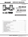
1
MD-MX30/MX30W
SERVICE MANUAL
No.S4025MDMX30//
MD-MX30
MD-MX30 MD Compact Component System
consisting of MD-MX30(main unit) and CPMX30(speaker system).
MD-MX30W
MD-MX30W MD Compact Component System
consisting of MD-MX30W(main unit) and CPMX30W(speaker system).
(MD-MX30W only)
• In the interests of user-safety the set should be restored to its original
condition and only parts identical to those specified should be used.
CONTENTS
Page
SAFETY PRECAUTION FOR SERVICE MANUAL (FOR MD-MX30W) ............................................................................ 2
IMPORTANT SERVICE NOTES (FOR U.S.A. ONLY) ....................................................................................................... 3
VOLTAGE SELECTION (FOR MD-MX30W) ..................................................................................................................... 3
SPECIFICATIONS (FOR MD-MX30) ................................................................................................................................. 4
SPECIFICATIONS (FOR MD-MX30W) .............................................................................................................................. 5
NAMES OF PARTS ........................................................................................................................................................... 6
OPERATION MANUAL ...................................................................................................................................................... 8
DISASSEMBLY ................................................................................................................................................................ 10
REMOVING AND REINSTALLING THE MAIN PARTS ................................................................................................... 12
TEST MODE .................................................................................................................................................................... 15
ADJUSTMENT ................................................................................................................................................................. 20
EEPROM WRITING PROCEDURE ................................................................................................................................. 28
EXPLANATION OF ERROR DISPLAY ............................................................................................................................ 30
NOTES ON SCHEMATIC DIAGRAM .............................................................................................................................. 31
TYPE OF TRANSISTOR AND LED ................................................................................................................................. 31
BLOCK DIAGRAM ........................................................................................................................................................... 32
SCHEMATIC DIAGRAM / WIRING SIDE OF P.W.BOARD ............................................................................................. 37
WAVEFORMS OF CD CIRCUIT ...................................................................................................................................... 65
WAVEFORMS OF MD CIRCUIT ..................................................................................................................................... 66
TROUBLESHOOTING (CD SECTION) ........................................................................................................................... 68
TROUBLESHOOTING (MD SECTION) ........................................................................................................................... 72
FUNCTION TABLE OF IC ................................................................................................................................................ 76
REPLACEMENT PARTS LIST/EXPLODED VIEW/PACKING OF THE SET (FOR U.S.A.)
SHARP CORPORATION
–1–
This document has been published to be used
for after sales service only.
The contents are subject to change without notice.
MD-MX30/MX30W
SAFETY PRECAUTION FOR SERVICE MANUAL(For MD-MX30W)
WARNINGS (CD)
WARNINGS (MD)
THE AEL (ACCESSIBLE EMISSION LEVEL) OF THE LASER POWER
OUTPUT IS LESS THAN CLASS 1 BUT THE LASER COMPONENT
IS CAPABLE OF EMITTING RADIATION EXCEEDING THE LIMIT
FOR CLASS 1. THEREFORE IT IS IMPORTANT THAT THE
FOLLOWING PRECAUTIONS ARE OBSERVED DURING
SERVICING TO PROTECT YOUR EYES AGAINST EXPOSURE TO
THE LASER BEAM.
1-WHEN THE CABINET IS REMOVED, THE POWER IS TURNED
ON WITHOUT A COMPACT DISC IN POSITION AND THE PICKUP
IS ON THE OUTER EDGE THE LASER WILL LIGHT FOR
SEVERAL SECONDS TO DETECT A DISC. DO NOT LOOK INTO
THE PICKUP LENS.
2-THE LASER POWER OUTPUT OF THE PICKUP UNIT AND
REPLACEMENT SERVICE PARTS ARE ALL FACTORY PRESET BEFORE SHIPMENT.
DO NOT ATTEMPT TO RE-ADJUST THE LASER PICKUP UNIT
DURING REPLACEMENT OR SERVICING.
3-UNDER NO CIRCUMSTANCES STARE INTO THE PICKUP LENS
AT ANY TIME.
4-CAUTION-USE OF CONTROLS OR ADJUSTMENTS, OR
PERFORMANCE OF PROCEDURES OTHER THAN THOSE
SPECIFIED HEREIN MAY RESULT IN HAZARDOUS RADIATION
EXPOSURE.
The AEL (ACCESSIBLE EMISSION LEVEL) of the laser power
output is less than class 1 but the laser component is capable
of emitting radiation exceeding the limit for class 1. Therefore it is
important that the following precautions are observer during
servicing to protect your eyes against exposure to the laser beam.
1) When the unit case cover is removed and LOADING SW (SW
1956) is turned on and then PLAY SW (SW 1954 mechanism
PWB) is turned on in a few second.
The laser will light for several second to detect a disk.
2) The laser power output of the pickup unit and replacement service
parts are all factory pre-set before shipment.
Do not attempt to re-adjust the laser pickup unit during replacement
or servicing.
3) Under no circumstances stare into the pickup lens at any time.
4) If laser optical unit becomes faulty, replace the complete laser
optical unit.
5) CAUTION-USE of controls or adjustments, or performance of
procedures other than those specified herein may result in
hazardous radiation exposure.
CAUTION
Laser Diode Properties
Material:
Wavelength:
Emission Duration:
Laser Output:
GaAlAs
780 nm
continuous
max. 0.6 mW
● This MD Compact Component System is classified as a CLASS 1 LASER product.
● The CLASS 1 LASER PRODUCT label is located on the rear cover.
● Use the MD Compact Component System only in
accordance with the instructions given in this
manual and do not attempt to interfere with the
interlock switch or make any other adjustment as
this may result in exposure to hazardous radiation.
Laser Diode Properties
● Material:
GaAlAs
● Wavelength: 785 nm
● Pulse time:
Read mode: 0.8 mW Continuous
Write mode: max. 10 mW 0.5S
min. cycle 1.5S
Repetition
CAUTION-INVISIBLE LASER RADIATION WHEN OPEN. DO NOT STARE INTO BEAM
OR VIEW DIRECTLY WITH OPTICAL INSTRUMENTS.
CAUTION - INVISIBLE LASER RADIATION WHEN OPEN AND INTERLOCKS DEFEATED
AVOID EXPOSURE TO BEAM .
VARNING-OSYNLIG LASERSTRALNING NAR DENNA DEL AR OPPNAD. STIRRA EJ
IN I STRALEN OCH BETRAKTA EJ STRALEN MED OPTISKA INSTRUMENT.
VARNING - OSYNLIG LASERSTR LNING N R DENNA DEL R …PPNAD OCH SP RRAR
R URKOPPLADE. STR LEN R FARLIG.
ADVARSEL - USYNLIG LASERSTR LING N R DEKSEL PNES OG SIKKERHEDSL S
BRYTES. UNNG EKSPONERING FOR STR LEN.
ADVERSEL-USYNLIG LASERSTRALING VED ABNING. SE IKKE IND I
STRALEN-HELLER IKKE MED OPTISKE INSTRUMENTER.
VARO! AVATTAESSA JA SUOJALUKITUS OHITETTAESSA OLET ALTTIINA
N KYM T…N LASERS TEILYLLE. L KATSO S TEESEN.
VARO! AVATTAESSA OLET ALTTIINA NAKYMATON LASERSATEILYLLE. ALA
TUIJOTA SATEESEEN ALAKA KATSO SITA OPTISEN LAITTEEN LAPI.
VARNING - OSYNLIG LASERSTR LING N R DENNA DEL R …PPNAD OCH SP RREN
R URKOPPLAD. BETRAKTA EJ STR LEN.
VARNING-OSYNLIG LASERSTRALNING NAR DENNA DEL AR OPPNAD. STIRRA EJ
IN I STRALEN OCH BETRAKTA EJ STRALEN GENOM OPTISKT INSTRUMENT.
ADVERSEL-USYNLIG LASERSTRALING NAR DEKSEL APNES. STIRR IKKE INN I
STRALEN ELLER SE DIREKTE MED OPTISKE INSTRUMENTER.
ADVARSEL - USYNLIG LASERSTR LING VED BNING N R SIKKERHEDSAFBRYDERE
ER UDE AF FUNKTION. UNDG UDSETTELSE FOR STR LING.
–2–
MD-MX30/MX30W
FOR A COMPLETE DESCRIPTION OF THE OPERATION OF THIS UNIT, PLEASE REFER
TO THE OPERATION MANUAL.
IMPORTANT SERVICE NOTES (For U.S.A.Only)
BEFORE RETURNING THE AUDIO PRODUCT
(Fire & Shock Hazard)
Before returning the audio product to the user, perform the
following safety checks.
1. Inspect all lead dress to make certain that leads are not
pinched or that hardware is not lodged between the chassis
and other metal parts in the audio product.
2. Inspect all protective devices such as insulating materials,
cabinet, terminal board, adjustment and compartment
covers or shields, mechanical insulators etc.
3. To be sure that no shock hazard exists, check for leakage
current in the following manner.
* Plug the AC line cord directly into a 120 volt AC outlet.
* Using two clip leads, connect a 1.5k ohm, 10 watt resistor
paralleled by a 0.15µF capacitor in series with all exposed
metal cabinet parts and a known earth ground, such as
conduit or electrical ground connected to earth ground.
* Use a VTVM or VOM with 1000 ohm per volt, or higher,
sensitivity to measure the AC voltage drop across the
resistor (See diagram).
* Connect the resistor connection to all exposed metal parts
having a return path to the chassis (antenna, metal cabinet,
screw heads, knobs and control shafts, escutcheon, etc.)
and measure the AC voltage drop across the resistor.
VTVM
AC SCALE
1.5k ohms
10W
0.15 µ F
TO EXPOSED
METAL PARTS
TEST PROBE
CONNECT TO
KNOWN EARTH
GROUND
All check must be repeated with the AC line cord plug connection
reversed.
Any reading of 0.3 volt RMS (this corresponds to 0.2 milliamp.
AC.) or more is excessive and indicates a potential shock
hazard which must be corrected before returning the audio
product to the owner.
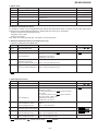
VOLTAGE SELECTION(For MD-MX30W)
The voltage selector is located on the AC voltage selector box. If adjustment is necessary, ensure to remove plug of AC cord from
AC socket and use a screwdriver in order to turn the selector in either direction. The correct voltage figure is displayed in the window
below to the adjustment screw.
QACCB0008AW00
QACCA0004AW00
QACCE0007AW00
QACCL0002AW00
QACCJ0006AW00
Figure 3 POWER SUPPLY CORD
–3–
MD-MX30/MX30W
SPECIFICATIONS (For MD-MX30)
● General
Power source:
Power
consumption:
Dimensions:
Weight:
● Compact disc player section
AC 120 V, 60 Hz
Type:
Drawer type compact disc player
Signal readout:
Non-contact,
laser pickup
Width; 8-1/2" (215 mm)
Height; 6-7/16" (162 mm)
Depth; 13-1/2" (342 mm)
Rotation speed:
200 - 500 rpm CLV, Approx.
Error correction:
CIRC (Cross Interleave Reed-Solomon Code)
10.4 Ibs. (4.7 kg)
Quantization:
16-bit linear
Frequency
response:
20 - 20,000 Hz
D/A converter:
1-bit D/A converter
73W
● Amplifier section
Output power:
FTC 20 watts per channel minimum
RMS into 6 ohms from 60 Hz to 20 kHz
with no more than 10 % total harmonic
distortion
semiconductor
Signal/noise ratio: 95 dB (1 kHz)
Output terminals: Speaker; 6 ohms
Headphones; 16 - 50 ohms
(recommended 32 ohms)
Input terminals:
3-beam
Auxiliary; 500 mV/47 k ohms
Dynamic range:
90 dB (1 kHz)
Wow and flutter:
Unmeasurable
(less than 0.001% W. peak)
● Tuner section
Frequency range: FM; 87.5 - 108.0 MHz
AM; 530 - 1,720 kHz
● MiniDisc recorder section
Sensitivity:
Type:
MiniDisc recorder
Signal readout:
Non-contact,
laser pickup
Rotation speed:
400 - 900 rpm CLV, Approx.
Error correction:
ACIRC (Advanced Cross Interleave ReedSolomon Code)
Quantization:
20-bit linear (A/D converter)
Coding:
ATRAC (Adaptive Transform Acoustic Coding)
Sampling
frequency:
44.1 kHz
3-beam
FM; 2.5 µV (75 ohms unbalanced)
AM; 650 µV/m
semiconductor
● Speaker section
Type:
2-way speaker system
[4-3/4" (12 cm) woofer and
3/4" (2 cm) tweeter]
Maximum input
power:
50 W
Rated input
power:
25 W
Impedance:
6 ohms
Magnetic modulation
overwrite method
Dimensions:
Frequency
response:
Width; 6-5/16" (160 mm)
Height; 11-1/16" (280 mm)
Depth; 9-1/4" (233.5 mm)
20 - 20,000 Hz
Weight:
7.1 Ibs. (3.2 kg)/each
D/A converter:
1-bit D/A converter
Wow and flutter:
Unmeasurable
(less than 0.001% W. peak)
Recording
method:
Signal/noise ratio: 95 dB (1 kHz)
Dynamic range:
90 dB (1 kHz)
Audio channel:
Stereo; 2 channels
Monaural; 1 channel (playback only)
(long-time recording mode)
Specifications for this model are subject to change without
prior notice.
–4–
MD-MX30/MX30W
SPECIFICATIONS (For MD-MX30W)
● General
Power source:
Power
consumption:
Dimensions:
Weight:
● Compact disc player section
AC 110/127/220/230-240 V, 50/60 Hz
70 W
Width; 215 mm (8-1/2")
Height; 162 mm (6-7/16")
Depth; 342 mm (13-1/2")
5 kg (11.0 lbs.)
● Amplifier section
Output power:
PMPO; 400 W (Total)
MPO; 96 W (48 W+48 W) (10% T.H.D.)
RMS; 50 W (25 W+25 W) (10% T.H.D.)
Type:
Drawer type compact disc player
Signal readout:
Non-contact, 3-beam semiconductor laser pickup
Rotation speed:
200 - 500 rpm CLV, Approx.
Error correction:
CIRC (Cross Interleave Reed-Solomon Code)
Quantization:
16-bit linear
Frequency
response:
20 - 20,000 Hz
D/A converter:
1-bit D/A converter
Signal/noise ratio: 95 dB (1 kHz)
Output terminals: Speaker; 6 ohms
Headphones; 16 - 50 ohms
(recommended 32 ohms)
Input terminals: Auxiliary; 500 mV/47 k ohms
Dynamic range:
90 dB (1 kHz)
Wow and flutter:
Unmeasurable
(less than 0.001% W. peak)
● Tuner section
● MiniDisc recorder section
Frequency range: FM; 88 - 108.0 MHz
AM; 531 - 1,602 kHz
Type:
MiniDisc recorder
Sensitivity:
Signal readout:
Non-contact, 3-beam semiconductor laser pickup
Rotation speed:
400 - 900 rpm CLV, Approx
● Speaker section
Error correction:
ACIRC (Advanced Cross Interleave ReedSolomon Code)
Type:
Quantization:
20-bit linear (A/D converter)
Coding:
ATRAC (Adaptive Transform Acoustic Coding)
Maximum input
power:
50 W
44.1 kHz
Rated input
power:
25 W
Impedance:
6 ohms
Dimensions:
Width; 160 mm (6-5/16")
Height; 280 mm (11-1/16")
Depth; 233.5 mm (9-1/4")
Weight:
3.2 kg (7.1 lbs.)/each
Sampling
frequency:
Recording
method:
Magnetic modulation
overwrite method
Frequency
response:
20 - 20,000 Hz
D/A converter:
1-bit D/A converter
Wow and flutter:
Unmeasurable
(less than 0.001% W. peak)
FM; 2.5 µV (75 ohms unbalanced)
AM; 650 µV/m
2-way speaker system
[12 cm (4-3/4") woofer and
2 cm (3/4") tweeter]
Signal/noise ratio: 95 dB (1 kHz)
Dynamic range:
90 dB (1 kHz)
Audio channel:
Stereo; 2 channels
Monaural; 1 channel (playback only)
(long-time recording mode)
Specifications for this model are subject to change without
prior notice.
–5–
MD-MX30/MX30W
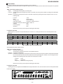
NAMES OF PARTS
■ Front panel
1.
2.
3.
4.
5.
6.
7.
8.
9.
10.
11.
12.
13.
14.
15.
16.
17.
18.
19.
20.
21.
22.
23.
24.
25.
26.
27.
28.
1
On/Stand-by Button
Timer Stand-by Indicator
Name/TOC Edit Button
Timer/Delete Button
Tuning Down/Review Button
MD Stop Button
MD Play/Pause Button
Tuning Up/Cue Button
Display (Demo) Button
MD Compartment
MD Eject Button
Jog Dial
Memory/Enter Button
CD Compartment
Record Button
CD MD Normal Speed Edit Button
CD MD High Speed Edit Button
CD Open/Close Button
CD Stop Button
CD Play/Pause Button
Headphone Socket
Surround Button
Preset Equalizer Button
Extra Bass Button
Tuner (Band) Button
Auxiliary Button
Volume Control
Volume Select Button
9
10
14
21
■ Rear panel(For MD-MX30)
1.
2.
3.
4.
5.
6.
2 3 4
5 6 7 8
11
15 16
12
17 18 19 20
25 26
22 23 24
27
MD-MX30
FM 75 Ohms Antenna Terminal
Antenna Ground Terminal
AM Loop Antenna Terminal
Auxiliary Input Jacks
Speaker Terminals
AC Power Input Jack
1 2 3 4
5
■ Rear panel(For MD-MX30W)
1.
2.
3.
4.
5.
6.
7.
8.
6
FM 75 Ohms Aerial Terminal
Aerial Earth Terminal
AM Loop Aerial Terminal
Auxiliary Input Sockets
Span Selector Switch
Speaker Terminals
AC Power Input Socket
AC Voltage Selector
MD-MX30W
1
2 3 4 5
7
–6–
8
13
6
28
MD-MX30/MX30W
Display window
1. FM Stereo Indicator
2. FM Stereo Mode Indicator
3. Track Edit Indicator
4. Play/Pause Indicator
5. Repeat Indicator
6. TOC Indicator
7. Level Meters
8. Digital Recording Indicator
9. CD Indicator
10. High Speed Edit Indicator
11. MD Indicator
12. Record Indicator
13. Sleep Indicator
14. Disc Indicator
15. Track Indicator
16. Memory Indicator
17. Random Play Indicator
18. Total Time Indicator
19. Remaining Time Indicator
20. Character Information Display
21. AM/PM Indicator
22. Timer Record/Timer Play Indicator
23. Surround Indicator
24. Extra Bass Indicator
1
13
14
15
16
17
18
2 3 4 56
7
19
20
8 9
10 11
12
2122 23 24
Remote contorol
1. Remote Control Transmitter LED
2. Preset Equalizer Button
3. Surround Button
4. Clock Button
5. Sleep Button
6. Memory/Enter Button
7. MD Stop Button
8. MD Play/Pause Button
9. MD Track Down/Review Button
10. MD Track Up/Cue Button
11. Track Edit Button
12. Record Button
13. On/Stand-by Button
14. Dimmer Button
15. Tuner Preset Up/Down Buttons
16. Extra Bass Button
17. Volume Select Button
18. Display Button
19. Clear Button
20. Play Mode Button
21. Time Button
22. CD Play/Pause Button
23. CD Stop Button
24. CD Track Up/Cue Button
25. CD Track Down/Review Button
26. Tuner (Band) Button
27. Auxiliary Button
28. Volume Buttons
1
2
3
4
5
6
7
8
9
10
11
12
13
14
15
16
17
18
19
20
21
22
23
24
25
26
27
28
Speaker section
1.
2.
3.
4.
Tweeter
Woofer
Bass Reflex Duct
Speaker Terminals
–7–
1
3
2
4
Jog dial
MEMORY/
ENTER
–8–
5 Press the MEMORY/ENTER button.
"0:00"
→The 24-hour display will appear.
→(0:00 - 23:59)
"12:00 AM" →The 12-hour display will appear.
→(AM or PM 12:00 - 11:59)
"0:00 AM" →The 12-hour display will appear.
→(AM or PM 0:00 - 11:59)
● Note that this can only be set when the unit is
first installed or it has been reset.
4 Turn the jog dial to select the time display mode.
button.
3 Within 5 seconds, press the MEMORY/ENTER
2 Press the CLOCK button.
power on.
1 Press the ON/STAND-BY button to turn the
● In this example, the clock is set for the 24-hour
(0:00) system.
CLOCK
ON/STAND-BY
SETTING THE CLOCK
Press the CLOCK button.
Perform steps 6 - 9 above.
Within 5 seconds, press the MEMORY/ENTER
button.
1Reset the microcomputer.
2 Perform steps 2 - 9 above.
To change the time display mode:
3
1
2
To change the clock time:
Note:
● The "CLOCK" will appear at the push of the
CLOCK button when the AC power supply is restored after a power failure occurs or after the
AC power lead is disconnected.
If this happens, follow the procedure below to
change the clock time.
Press the CLOCK button.
● The time display will appear for about 5 seconds
even in the stand-by mode.
To see the time display:
● The clock starts operating from "0" second.
(Seconds are not displayed.)
9 Press the MEMORY/ENTER button.
● When the jog dial is turned one click clockwise,
the time will increase by 1 minute. When it is
turned one click anti-clockwise, the time will
decrease by 1 minute. Keep turning the jog dial
to change the time continuously.
● The hour setting will not advance even if minutes advance from "59" to "00".
●
●
●
●
● No sound is heard.
● Radios make unusual noise or the
picture on the TV screen is distorted.
● Did a power failure occur?
● The clock is wrong.
● When a button is pressed, the unit
does not respond.
Is the volume level is set to "0"?
Are the headphones connected?
Are the speaker wires disconnected?
When a radio or TV which uses an
indoor aerial is placed near the unit,
the picture on the TV screen may be
distorted or the radio may not function properly.
Possible cause
Symptom
General
● It is recommended that you use
an external aerial.
● Try setting it again.
● Set this unit to the stand-by
mode and then turn it back on.
Then, retry the operation.
● Increase the volume level.
● Disconnect the headphones.
● Connect the wires securely.
Remedy
If this unit functions abnormally during operation, first check the following items. If the unit continues to function
abnormally, or if an abnormality appears other than listed below, set this unit to the stand-by mode and disconnect the AC power plug, then consult your SHARP dealer or service personnel.
■ If a problem occurs
TROUBLESHOOTING
Caution:
● The operation explained above will erase all data
stored in memory including clock and timer
settings, and tuner, MiniDisc and CD presets.
2
8 Adjust the minutes by turning the jog dial.
2 Press the ON/STAND-BY button whilst holding
stand-by mode.
1 Press the ON/STAND-BY button to enter the
down the SURROUND button and the
TIMER/DELETE button.
● "ALL CLEAR" will appear.
1,2
2
If this product is subjected to strong external interference (mechanical shock, excessive static electricity, abnormal supply voltage due to lightning, etc.)
or if it is operated incorrectly, it may malfunction or
the display may not function correctly. If such a problem occurs, do the following:
7 Press the MEMORY/ENTER button.
● When the jog dial is turned one click clockwise,
the time will increase by 1 hour. When it is turned
one click anti-clockwise, the time will decrease
by 1 hour. Keep turning the jog dial to change
the time continuously.
● When the 12-hour display is selected, "AM" will
change to "PM" automatically.
6 Adjust the hour by turning the jog dial.
RESETTING THE MICROCOMPUTER
MD-MX30/MX30W
OPERATION MANUAL
● The disc is loaded up-side down.
● The disc is very dirty.
● The disc which does not satisfy the
standards.
● Is the unit located near excessive
vibrations?
● Has condensation formed inside the
unit?
● Even though a disc has been
loaded, "NO DISC" is displayed.
● Playback stops in the middle of a
track, or playback is not performed
properly.
● Playback sounds are skipped.
● The disc is very dirty.
● Is the unit located near excessive
vibrations?
● Has condensation formed inside the
unit?
● Even though a disc has been
loaded, "NO DISC" or "CAN'T
READ" is displayed.
● Playback sounds are skipped.
–9–
● The unit is placed near the TV or
computer.
● The aerial direction is not placed
properly.
● Did you erase the programmed station?
● Radios make unusual noise consecutively.
● The preset channel cannot be recalled.
● The batteries (polarity) are not inserted properly.
● The batteries inside the remote control are dead.
● The remote control is operated from
an incorrect distance or angle.
● Is the AC power lead plugged in?
● The remote control does not function or does not operate properly.
● The power cannot be turned on
from the remote control.
Possible cause
Symptom
Remote control
Possible cause
Symptom
● Insert properly.
● Replace the batteries.
● Operate it within a range of 0.2
m (8") to 6 m (20') and within an
angle of 15 ° to either side of
centre.
● Connect the AC power lead.
Remedy
● When the unit receives a radio
broadcast near a TV set, a computer or a word-processor, it may
pick up noise. If this happens,
move the unit from the place
where the noise is picked up.
● Correct the aerial direction.
● Preset the channel again.
● Redo programming.
Remedy
● Clean the disc.
● Place the unit on a firm, level
surface free from vibration.
● Remove the disc and leave the
power turned on. The unit
should function properly in
about 1 hour.
● Is the MiniDisc protected against
accidental erasure?
● Did you try to make recording on a
playback-only MiniDisc?
● Can you see the "DISC FULL" or
"TOC FULL" message in the display?
Radio reception
Remedy
● Slide the accidental erase prevention tab back to its original
position.
● Replace it with a recordable
disc.
● Put in another recordable disc
with recording space on it.
Possible cause
● A recording cannot be made.
● Load the disc with the correct
side up.
● Clean the disc.
● Load the correct disc.
● Place the unit on a firm, level
surface free from vibration.
● Remove the disc and leave the
power turned on. The unit
should function properly in
about 1 hour.
Remedy
Symptom
MiniDisc recording and playback
Possible cause
Symptom
CD Playback
(Continued)
● TOC information recorded on the MD
does not match the MiniDisc specifications or it cannot be read.
● There is no space left for recording
track numbers.
● There is no space left for recording
character information.
● The data contains an error.
● MiniDisc not specified.
TOC FORM
( :Number or
symbol)
TOC FULL
? DISC
TOC FULL 1
● The temperature is too high.
TEMP OVER
PROTECTED
PLAY MD
NOT AUDIO
NO DISC
Er-MD
( :Number or
symbol)
NAME FULL
● The number of characters for the disc
name or track name exceeds 40.
● A MiniDisc has not been loaded.
● The MiniDisc data cannot be read.
● A CD has not been loaded.
● The CD data cannot be read.
● The data recorded on this disc is not
audio data.
● You tried to record on a playback-only
disc.
● The disc is write protected.
● You chose 21 or more tracks for track
editing.
● There is no space to make CD editing
on the disc.
● A MiniDisc is not working properly.
E. OVER
EDIT OVER
● The CD tray is not working properly.
● The disc is out of recording space.
● Recording cannot be performed correctly due to vibration or shock in the
unit.
● The TOC information could not be created properly due to a mechanical
shock or to scratches on the disc.
E-CD 20
DISC FULL
CAN'T WRITE
CAN'T REC
Error messages
Meaning
BLANK MD
● Nothing is recorded.
(Neither music nor disc name is recorded.)
CAN'T COPY
● You tried to record from a copy prohibited CD.
CAN'T READ
● The disc is damaged.
( :Number or
● TOC information cannot be read.
symbol)
● MiniDisc not specified.
CAN'T EDIT
● A track cannot be edited.
When an error message is displayed, proceed as follows:
ERROR MESSAGES
● Replace it with another recordable
disc.
● Replace it with another recordable
disc.
● Erase the needless characters.
● Replace it with another disc.
● Load a MiniDisc.
● Reload the MiniDisc.
● Load a CD.
● Reload the CD.
● Select another track.
● Replace the disc.
● Replace it with another recordable
disc.
● Move the write protection tab back to
its original position.
● Set this unit to the stand-by mode and
wait for a while.
● Replace it with another disc.
● Erase the disc and try recording again.
● Shorten the disc or track name.
● Replace it with a disc that has enough
time to record.
● Set this unit to the stand-by mode and
turn the power on again.
● Set this unit to the stand-by mode and
try to write the TOC again. (Remove
any source of shock or vibration whilst
writing.)
● Replace the disc with another recordable disc.
● Set this unit to the stand-by mode and
turn the power on again.
● Decrease the number of tracks.
● Change the stop position of the track
and then try editing it.
● Re-record or replace the MiniDisc.
● Replace it with another disc.
● Erase the disc and try recording again.
● Replace the CD.
Remedy
● Replace it with another disc.
MD-MX30/MX30W
MD-MX30/MX30W
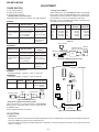
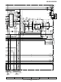
DISASSEMBLY
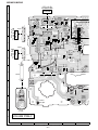
Notes for servicing (For MD-MX30 only)
• This model is equipped with a fan. If you remove the fan to
service the unit, it enters the protection mode and the
power cannot be turned on by pressing the POWER
button. In such a case, follow the procedure below.
(Refer to Fig.10-1.)
1. Check whether a resistor (RV 66,39ohm,1/2W) is inserted.If
not, connect it (39ohm,1/2W).
2. Connect the patterns circled with a dotted line by soldering.
Caution on Disassembly
The disassembling the machine or assembling it after
repair, observe the following instructions to ensure safety
and keep its performance.
1. Unload the compact disc, and mini-disc, cassette tape
from machine.
2. Be sure to unplug the power cable before starting
disassembly of the machine.
3. When disassembling each section, remove the nylon
band or wire arrangement.
After servicing the unit, be sure to rearrange the leads
where they were before disassembling.
If a screw of improper length is fit to the MD mechanism.
(A screw fit the part to the mechanism chassis of MD
section), it may contact the optical pickup, impeding
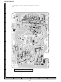
normal operation. Hence, due care must be taken.
4. While repairing, pay utmost attention to static electricity
on ICs.
• Desolder to reassemble the unit after repairing. If you fail
to desolder, the power turns off soon because the unit
enters the protection mode when the fan rotates at a high
speed (high power).
REMOVAL
PROCEDURE
FIGURE
1
Top Cabinet
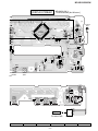
1. Screw ................ (A1) x7
10-2
2
Side Panel (Right,Left) 1. Screw ................ (B1) x8
10-2
3
Rear Panel
1. Socket ............... (C1) x1
2. Screw ................ (C2) x6
10-3
4
Main PWB
(Note 1)
1. Screw ................ (D1) x9
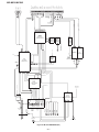
2. Flat Cable .......... (D2) x4
3. Socket ............... (D3) x3
11-1
CV15
2 3 4 5
RV20
RV19
LUGV01
CHASSIS
GND
1
CV01
RV60
BIV01
2
NSV02
11 - G,H
APLAY PWB
B
C
E
RV66
2 1
DV05
MAIN PWB-A1
QV54
RV03
CV62
RV59
V02
CV07
CV58
STEP
RV07
CV09
CV13
DV06 CNPV01
RV21
RV01
RV50
CV53
RV05
CV61
CV56
MAIN UNIT
3
2
1
RV11
RV09
CV05
QV51
RV53
RV51
B C E
RV15
DV03
RV17
• These steps are unnecessary to service the unit with the
fan connected.
CV59
RD
1
2
CNSV01
MV01
FAN MOTOR
Figure 10-1
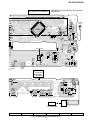
5
Tuner PWB
1. Screw ................ (E1) x4
11-1
6
Power PWBx2
1. Socket ............... (F1) x1
2. Screw ................ (F2) x9
11-2
MAIN UNIT
7
MD/CD Holder
1. Screw ................ (G1) x8
2. Flat Cable .......... (G2) x1
11-3
(A1) x2
ø3 x12mm
8
Front Panel
1. Screw ................ (H1) x4
11-4
9
Volume PWB
1. Knob .................. (J1) x1
2. Screw ................ (J2) x3
3.Nut ...................... (J3) x1
11-5
Illustration: MD-MX30
Cabinet
(B1) x2
ø3 x12mm
(A1) x2
ø3 x12mm
10
Display PWB
1. Knob .................. (K1) x1
2. Nut ..................... (K2) x1
3. Screw ................ (K3) x8
11-5
11
CD Servo PWB
(Note 1)
1. Socket ............... (L1) x5
2. Lug .................... (L2) x1
3. Screw ................ (L3) x3
11-6
12
MD Holder
(MD Unit)
1. Screw ................ (M1) x3
2. Screw ................ (M2) x4
11-6
13
CD Mechanism
1. Screw ................ (N1) x3
11-7
14
MD Mechanism
(Note 1)
1. Screw ................ (P1) x8
2. Flat Cable .......... (P2) x3
3. Flexible PWB .... (P3) x1
4. Socket ............... (P1) x2
12-1
(B1) x2
ø3 x12mm
Side
Panel(R)
(B1) x2
ø3 x12mm
(A1) x3
ø3 x12mm
(B1) x2
ø3 x12mm
Side Panel(L)
Figure 10-2
Note 1:
After removing the connector for the optical pickup from the
connector wrap the conductive aluminium foil around the
front end of connector so as to protect the optical pickup
from electrostatic damage.
(C1) x1
(C2) x6
ø3 x10mm
Rear Panel
Figure 10-3
– 10 –
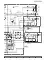
MD-MX30/MX30W
DISPLAY PWB
(D1) x4
ø3 x10mm
(D1) x1
ø2.6 x10mm
(K2) x1
Lug
(D1) x2
ø3 x10mm
(D2) x1
(K1) x1
Washer
DISPLAY PWB
(J1) x1
(D3) x1
MAIN PWB
(D1) x1
ø3 x10mm
VOLUME PWB
HOLDER PWB
(D1) x1
ø3 x10mm
Lug(MD-MX30 Only)
(D2) x2
(D2) x1
(D3) x1
(E1) x2
ø3 x10mm
(D3) x1
(J3) x1
Washer
TUNER PWB
(E1) x2
ø3 x10mm
Volume Holder
(J2) x3
ø3 x12mm
Figure 11-1
(F2) x2
ø3 x10mm
(K3) x8
ø2.6 x10mm
Figure 11-5
(F2) x4
ø4 x8mm
(M2) x2
ø3 x6mm
(M1) x1
ø2.6 x10mm
(L2) x1
(F1) x1
(F2) x1
ø3 x10mm
MD UNIT
(M1) x2
ø2.6 x10mm
HOLDER PWB
POWER PWB
(F2) x2
ø3 x10mm
(G1) x1
ø3 x10mm
(L1) x2
MD Holder
Figure 11-2
(G1) x4
ø3 x10mm
CD SERVO PWB
(G1) x1
ø3 x10mm
(L3) x3
ø3 x10mm
(G1) x2
ø3 x10mm
CD Roading
Chassis
(G2) x1
(L1) x1
(M2) x2
ø3 x6mm
Figure 11-6
(N1)x3
ø2.6 x10mm
MD/CD Holder
CD SERVO PWB
Figure 11-3
CD Roading
Chassis
Front Panel
Lug
(H1) x3
ø3 x10mm
(H1) x1
ø3 x10mm
CD Mechanism
Figure 11-4
Figure 11-7
– 11 –
(L1) x2
MD-MX30/MX30W
(P1)x1
ø2x 3mm
Shield Case,Top
SPEAKER
STEP
(P1)x1
ø2x 3mm
1
PROCEDURE
FIGURE
1. Net ..................... (A1) x1
2. Screw ................ (A2) x4
3. Screw ................ (A3) x6
12-2
12-3
REMOVAL
Net Frame
Woofer
Tweeter
(P1)x1
ø2x 3mm
MD MECHANISM
(P1)x1
ø2x 3mm
Shield Case,Side
(A1) x1
Figure 12-2
MD MAIN PWB
(P2)x2
(P4)x1
(P2)x1
Tweeter
Cusion Seet
(P4)x1
(A3) x4
ø4 x20mm
(P1)x2
ø1.7x 3mm
Pull
(P3)x1
Pull
Optical pickup
Flexible PWB
(Note 1)
(P1)x1
ø2x 3mm
(A2) x4
ø4 x20mm
Shield Case,Bottom
(P1)x1
ø2x 2mm
(Note 1) After removing the flexible PWB for optical pickup
from the connector wrap the front end of flexible PWB in
conductive aluminum foil so as to protect the optical pickup
from being damaged electrostatically.
Woofer
Figure 12-3
Figure 12-1
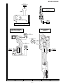
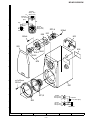
REMOVING AND REINSTALLING THE MAIN PARTS
MD MECHANISM SECTION
(A1)x1
ø1.7x 5mm
For details about the procedure to remove the MD mechanism
from the main unit, refer to the Disassembly Procedure, Steps
1-4,12 and 14 in the main unit and also the MD section.
(Referring to p.10-12)
Magnetic Head
Caution:
After pulling out the optical pickup connector, wrap the end
of the connector in conductive aluminium foil to prevent the
optical pickup from being destroyed by static electricity.
MD Mechanism
How to remove the magnetic head
(See Fig. 12-4)
1. Remove the screws (A1) x 1 pc.
Caution:
Take utmost care so that the magnetic head is not damaged
when it is mounted.
Figure 12-4
– 12 –
(A3) x2
ø4 x10mm
MD-MX30/MX30W
How to remove the MD loading PWB/loadeing
motor
(See Fig. 13-1)
(B1)x1
ø1.7x 6mm
1. Remove the screw (B1) x 1 pc.
2. Remove the Hoock (B2) x 3 pcs., and remove the MD
Loading PWB.
3. Remove the screw (B3) x 2 pcs., and remove the Loading
motor.
Loading Motor
Loading Motor PWB
(B2)x1
(B2)x2
(B3)x2
ø1.7x 3mm
Figure 13-1
(C1)x1
ø1.4x 5mm
How to remove the sled motor/optical pickup
(See Fig. 13-2)
Optical Pickup
1. Remove the screws (C1) x 3 pcs., and remove the sled
motor.
2. Remove the optical pickup.
(C1)x2
ø1.4x 4.5mm
Washer
Caution:
Be careful so that the gear is not damaged.
(The damaged gear emits noise during searching.)
Sled Motor
Mechanism Switch PWB
Figure 13-2
How to remove the spindle motor
(See Fig. 13-3)
(D1)x3
ø1.4x 3mm
1. Remove the screws (D1) x 3 pcs., and remove the spindle
motor.
Spindle Motor
Caution:
Be careful so that the gear is not damaged.
(The damaged gear emits noise during searching.)
Figure 13-3
– 13 –
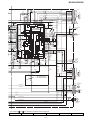
MD-MX30/MX30W
CD MECHANISM SECTION
( A1 ) x2
ø2.6 x 6 mm
For details about the procedure to remove the CD mechanism
from the main unit, refer to Disassembly Procedure, Steps 14 ,7 and 11-13 in the main unit and also the CD section.
(p.10,11).
Optical Pickup
CD Mechanism
How to remove the optical pickup
(See Fig. 14-1.)
Stop Washer
( A3 ) x1
1. Remove the screws (A1)x 2 pcs., to remove shaft (A2)x 1
pc.
2. Remove the stop washer (A3)x 1 pc., to remove the gear
(A4)x 1 pc.
3. Remove the optical pickup.
Gear
( A4 ) x1
Shaft
( A2 ) x1
Figure 14-1
Note:
After disconnecting the optical pickup connector wrap the
front end of connector in conductive aluminium foil to
prevent damage to the optical pickup by static electricity.
(B2) x 2
ø2 x 4mm
How to remove the CD loading motor
(See Fig. 14-2.)
1. Remove the belt (B1)x 1 pc.
2. Remove the screws (B2)x 2 pcs.,and remove the Loading
motor.
CD Unit
Belt
(B1) x 1
CD Roading Motor
Figure 14-2
How to remove the disc tray
(See Fig. 14-3/4 .)
1. Rotate the disc tray gear in the direction of the arrow (1). Pull
out the disc tray as shown by the arrow (2).
2. Press the right and left claws as shown by the arrow (3) to
remove the disc tray.
Disc Tray Gear
1
2
Figure 14-3
claws
3
3
Figure 14-4
– 14 –
MD-MX30/MX30W
TEST MODE
Press specified buttons simultaneously to enter the following test modes.
System section
TEST 1: Factory setting (version number and destination)
TEST 2: Soft reset
MD section
TEST 3: MD test 1 (adjustment, test, etc.)
CD section
TEST 4: CD test
Tuner section
TEST 5: Tuner test frequency preset
TEST 6: Tuner preset clear
Entering the test mode
While holding down the following 2 buttons, press the ON/STAND-BY button to enter each test mode.
Level meter
"Center Bar"
Name
Description
Button1
Button2
TEST1
Factory setting
–
Setting the unit to default.
[SURROUND]
[ENTER]
TEST2
Soft reset
–
Reinitializing the unit.
[SURROUND]
[DELETE]
TEST3
MD test 1
Flashing
Setting MD microcomputer to test mode
[SURROUND]
[MD-PLAY]
TEST4
CD test
Flashing
Testing CD mechanism, hard
[X-BASS]
[>>]
TEST5
Tuner test
–
Presetting test frequency
[TUNER]
[MD-PLAY]
–
Clearing all preset settings
[TUNER]
[MD-STOP]
Frequency preset
TEST6
Tuner preset clear
Table 15-1 Test mode entry
System section
TEST 1 Factory setting test mode
Object:
Putting the unit in default state.
Function: Checking existence of CD and MD and reinitializing all functions.
Operation: The unit performs CD initial operation and checks existence of CD.
If a CD exists, "CD OPEN" appears and tray opens in CD mode then the unit enters the normal power-on state.
Ejecting MD
While disc existence check, program version and preset destination appear according to the display.
When disc existence check is completed, the unit reinitializes all settings and displays "FINISH" according to the display and
prohibits every button input including power supply operation.
Leaving the test mode
The unit returns to normal operation by connecting and disconnecting the power supply cord.
Item
Type
Sub-display
Version and destination display
1
V
2
3
Character display
5
6
7
8
H
Number
O P E N
4
*
CD presence
Operation
C
D
Setting end
Function
F
I
N
* *
I
S
H
Table 15-2 Character display
Destination is displayed by its name.
– 15 –
:
:
9
10 Sub-display
Remarks
MD-MX30/MX30W
TEST 2 Soft reset
Object:
Reinitializing the unit.
Function: Reinitializing all functions.
Operation: "ALL CLEAR" appears and the unit reinitializes all functions and then turns power on.
Leaving the test mode
After reinitializing by soft reset, the unit enters the normal power-on state.
Item
Type
Sub-display 1
A
Reset operation display Operation
2
L
3
L
4
Character display
5
6
7
8
C L E A
:
9
R
10 Sub-display
Remarks
Table 16-1 Character display
MD section
TEST 3 MD test 1
Object:
Setting the MD unit to test mode.
Function: Setting the MD microcomputer to test mode, sending test commands which correspond to the button entry, and
displaying indication data from the microcomputer.
Operation: Power turns on and the mode is switched to MD by entering the test mode.
The test mode setting command is sent to the MD microcomputer to enter the test mode.
Button entries not in theTable 17 (page 17) are ignored.
10 characters data received from the MD microcomputer are displayed.
EJECT and LOADING are operated normally.
Disc can be loaded or unloaded forcibly by VOLUME up and down operations while MD microcomputer version is displayed
in disc chucking and while EJECT is displayed.
Leaving the test mode
Pressing the ON/STAND-BY button turns the power off normally.
No auto adjustment mode setting
While in this test mode, pressing the MEMORY/ENTER button switches the unit to the no auto adjustment operation mode
as follows.
The unit enters the no auto adjustment operation mode after the above. As normal operation, every button input is valid.
While this setting, "Center bar" should flash. The unit is in the test mode continuously.
Note:
In no auto adjustment operation mode, the mode is canceled by pressing the ON/STAND-BY button. When power turns on
again, normal power-on operation is performed.
– 16 –
MD-MX30/MX30W
Button to press
Press
Main unit Remote control
[ON/STAND-BY]
Once
Function
Power on and off. Turns the power off when POWER ON and on
when POWER OFF.
Sending test mode menus. To servo adjustment mode.
(Menus concerning adjustment and EEPROM.)
Sending test mode menus. To recording mode.
(Menus concerning continuous playback and continuous recording.)
Sending test mode menus. To other modes.
(INNER mode menu, JUMP SELECT menu, etc.)
Sending menus backward in each mode.
(Valid in each test mode.)
[EQUALIZER]
Once
[X-BASS]
Once
[CD-PLAY]
Once
[CD-STOP]
Once
[MD-PLAY]
Once
Menu selection and execution.
[MD-STOP]
Once
Stopping each test item and returning to the previous selection menu.
[UP]
Once
1) Sled motor moving outward (FWD) and continuation.
Continuously 2) JUMP.
3) Address value UP.
Others
[DOWN]
Once
1) Slide motor moving inward (REV) and continuation.
Continuously 2) JUMP.
3) Address value DOWN.
Others
[VOLUME UP]
–
[VOLUME DOWN]
–
[DISPLAY]
Once
[MEMORY/ENTER]
Once
To the no auto adjustment operation mode.
LOADING SW
–
Normal loading.
[EJECT]
Once
Normal eject.
1) Forcibly disc unloading.
2) Adjustment value + 1.
1) Forcibly disc loading.
2) Adjustment value - 1.
1) Laser switching at "EJECT".
2) Display switching when continuous playback.
Others
Table 17 Button entry table
Display in the MD test mode 1
"Center Bar" of the level meter flashes during this mode.
Lower-case characters appear according to the 10-letter data from the MD microcomputer.
When an MD disc is already loaded: "_AUT_YOBI_" appears.
The entry to this mode becomes steady when the indication appears as the AUTO YOBI mode Figure 17-1
"_AUTO_YOBI_" indication when entering MD test mode
Figure 17-1
– 17 –
MD-MX30/MX30W
When an MD is not loaded: "_EJECT_" appears.
Indication appears as shown in Figure 18-1 when a disc is not loaded.
When a disc is loaded, the MD microcomputer enters the AUTO YOBI mode. The received character data will be displayed
as Figure 17-1 (page 17).
"_EJECT_" indication when entering the MD test mode
Figure 18-1
Indication when moving to the normal power-off mode in the no auto adjustment mode.
When the MEMORY/ENTER button is pressed in this mode, the unit leaves this test mode and becomes normal power-on
state in the no auto adjustment mode.(This mode is used for technical consideration, not for service.)
After displaying "POWER ON", "MD DISC" (Figure 18-2) appears then the normal power-on indication appears.
"MD DISC" display
Figure 18-2
CD section
TEST 4 CD test mode
When focus is not correct in step 3 or when entering other
error correction modes, the unit cannot move to the next
step.
When the unit enters error correction mode, press the ON/
STAND-BY button to stop the test mode or the CD-STOP
button to return to step 1. Other operations are prohibited.
CD test mode flow chart
Entry
Step1
Slide
Memory
CD-Stop Step2
Laser output
Press the ON/STAND-BY button in each step to cancel the
test mode and return to the normal POWER OFF.
CD-Play
CD-Play
Memory
CD-Stop Step3
Focus search
CD-Play
Memory
CD-Stop Step4
CLV
CD-Play
Memory
CD-Stop Step5
Manual playback
CD-Play
Step7
Overall test
Table 18
– 18 –
MD-MX30/MX30W
Tuner section
Pressing the specified buttons performs the following 3 test operations.
The operations are performed when POWER ON. When they are completed, the unit enters the normal power-on operation
state.
TEST 5 Tuner test frequency preset
Object:
Presetting the test frequency for factory test.
Function: Presetting bands and frequencies shown in the Table 19 to each preset number according to the destination
default.
Operation: The bands and frequencies shown in the table are preset by entering test mode and power turns on in the
following state.
Function:
Band:
Tuning mode:
Call preset number:
Each band last preset channel:
X-BASS:
Preset equalizer:
Surround:
Tuner
FM monaural
Preset call tuning
Frequency of preset number 1
Refer to Table 19
OFF
FLAT
OFF
Others are set to the previous power-off setting (the last state).
Leaving the test mode
When frequency is preset in the specified state, the unit turns on normally and returns to the normal operation state.
MD-MX30
AM
FM
1
2
3
4
5
6
7
8
9
10
87.5MHz 108.0MHz 90.0MHz 106.0MHz 98.0MHz
530kHz
1720kHz
600kHz
1400kHz
990kHz
MD-MX30W
1
87.5MHz
2
108.0MHz
FM
3
90.0MHz
4
106.0MHz
5
98.0MHz
6
531kHz
7
1602kHz
AM
8
603kHz
9
1404kHz
10
990kHz
Table 19 TEST_TuSet preset frequency table
All FM bands are preset to FM monaural.
TEST 6 Tuner preset clear test
Object:
Clearing all presetttings.
This function is opened to the users in the operation manual.
Function: Canceling all presettings.
Operation: "PRESET CL" appears by entering test mode. All tuner preset memories are cleared. Last preset information,
etc. for each band are also returned to initial state and all presettings are cleared. The unit changes the last
settings of the following items and enters the normal power-on state.
Function:
Band:
Frequency:
Tuner
FM-Stereo
Minimum receiving frequency
Others are set to the previous power-off setting (the last state).
Leaving the test mode
Clearing presets are completed and POWER ON in the specified state. Then, the unit returns to the normal operation state.
Preset clear display
Figure 19-1
– 19 –
MD-MX30/MX30W
ADJUSTMENT
TUNER SECTION
fL: Low-range frequency
fH: High-range frequency
fC: Center-range frequency
• AM adjustment and confirmation
AM signal oscillator Frequency 400 Hz, 30%, AM modulation
MD-MX30
Adjusting item
• Setting the Test Mode
While holding down the TUNER(BAND) button and the MD
PLAY button, press the ON/STAND-BY button. Frequencies
are rewritten in memory as shown in table 18. Call them using
the JOG DIAL for tuner circuit adjustment and check.
Note that once you reinitialize the settings, the frequencies
recorded by users will be changed.
Adjusting
method
Adjusting object
IF
Adjust the indication of Set IF waveform
T351 set to 1,720 kHz. 450 kHz to maximum.
Frequency cover
(VT line voltage of
TP301)
fL: T306 (530 kHz)
Adjust the indication
of set to 530 kHz.
fH: (1,720 kHz)
fL: 1.3 ± 0.1 V
fH: 8.5 ± 1.3 V
(Only confirmation)
Tracking
fC: T302 (990 kHz)
Set the output of
speaker terminal
to maximum.
Preset No.
P01
P02
P03
P04
P05
Frequency
Frequency
(MD-MX30)
Preset No.
87.5 MHz
108.0 MHz
90.0 MHz
106.0 MHz
98.0 MHz
P06
P07
P08
P09
P10
Frequency
(MD-MX30W)
530 kHz
1,720 kHz
600 kHz
1,400 kHz
990 kHz
531 kHz
1,602 kHz
603 kHz
1,404 kHz
990 kHz
Table 20
AM Loop Antenna
MD-MX30W
Adjusting item
IF
IF:Speaker Terminal Electronic
Freqency cover:TP301 voltmeter
Adjusting
method
Adjusting object
AM signal oscillator
Adjust the indication of Set IF waveform
T351 set to 1,620 kHz. 450 kHz to maximum.
Frequency cover
(VT line voltage of
TP301)
fL: T306 (522 kHz)
Adjust the indication
of set to 522 kHz.
fH: (1,620 kHz)
fL: 1.3 ± 0.1 V
fH: 8.5 ± 1.3 V
(Only confirmation)
Tracking
fC: T302 (990 kHz)
Set the output of
speaker terminal
to maximum.
UNIT
GND
Figure 20-1 AM IF/Frequency Cover
TUNER PWB-A3
IC303
13
14
15
16
17
18
19
20
21
22
23
24
• FM mute level adjustment
MD-MX30:
FM signal oscillator Frequency 1 kHz, 67.5 kHz dev.
MD-MX30W:
FM signal oscillator Frequency 1 kHz, 40 kHz dev.
Frequency
Adjusting
method
Adjusting
object
98 MHz
26 dB(EMF)
VR351
SO301A
CF352
T351
AM IF
CF302
Adjusting object
FM MUTE
LEVEL
VR351
Input: SO301B
Output: Speaker
Terminal
Speaker Terminal
12
11
10
9
8
7
6
5
4
3
2
1
TP301
T306
OSC.AM
Electronic
voltmeter
IC302
FE301
FM signal oscillator
UNIT
T302
AM ANT.
12
13
14
15
16
17
18
19
20
21
22
11
10
9
8
7
6
5
4
3
2
1
Figure 20-2 FM Mute Level
• Erasing the registered broadcast station
When the power is off, press and hold the TUNER(BAND)
button and the MD STOP button, and then press the ON/
STAND-BY button.
All the registered stations are erased.
SO301B
SO301A
ANTENNA
TERMINAL
Figure 20-3 ADJUSTMENT POINT
CD SECTION
• Adjustment
Since this CD system incorporates the automatic adjustment functions, readjustment is not needed when replacing the pickup.
Therefore, PWBs and pickups can be combined freely.
Each time a disc is changed, automatic adjustment is performed. Therefore, playback of each disc can be performed under
optimum conditions.
– 20 –
MD-MX30/MX30W
MD SECTION
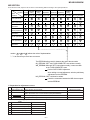
Enter the test mode, adjust or set as shown in the following table according to the repair operations.
Checking Writing the AUTO-YOBI
Execution item TEMP
AUTOAUTO-FAB Writing the
Operation check
EEPROM
EEPROM
EEPROM
required
adjustment
adjustment
adjustment
setting
basic setting
setting
setting
Repair
TEMP EEPROM_SET TEST-CANCEL AUTO–YOBI AUTO–ADJ AUTO–FAB TEST-CANCEL TEST-PLAY TEST-REC
operations
1
PICK replacement
2
3
4
5
6
7
1
HEAD replacement
MECHANISM
replacement
MAIN PWB
assembly replacement
8
1
MD microcomputer
replacement
1
2
3
4
5
6
7
8
2
3
4
5
6
7
8
9
2
3
4
5
3
4
5
6
1
1
MD LSI replacement
2
RF IC replacement
1
2
3
4
5
6
7
8
9
EEPROM IC
replacement
1
2
3
4
5
6
7
8
9
number
1 to 8 and 9 indicate the order of inplementation.
" – " is an item that you don't have to execute.
The EEPROM writing result is shown at the end of the test mode
OK_EEPROM: "SET" and "YOBI COMPLETE" were written normally
WR_EEPROM: Although "SET" was written normally, it was not written
in the "YOBI COMPLETE" state.
Peform "AUTO-YOBI" adjustment.
After making a normal adjustment, write the preliminary
adjustment into the EEPROM.
NG_EEPROM: "SET" could not be written.
Check the connection between the MD microcomputer
and the EEPROM.
1. Preparation for adjustment Test disc
Type
1
2
3
4
Part No.
Test disc
High reflection disc TGYS1 (SONY) [for Playback]
Low reflection disc Recording minidisc
SONY 80 minutes disc is recommended.(example:PRISM 80)
Head Adjusting transparent
Low reflection disc Pre-adjustment disc [TEAC Test MD]
Extension Cable (See Fig. 29)
1
2
3
4
5
Type
Part No.
Extension PWB for servicing
Extension Connector (2 Pin)
Extension Cable (6 Pin)
Extension Cable (5 Pin)
Extension Cable (28 Pin)
RUNTK0532AFZZ
QCNWK0129AFZZ
QCNWK0130AFZZ
QCNWK0109AFZZ
QCNWK0108AFZZ
– 21 –
RRCDT0101AFZZ
––––––––––––
RRCDT0103AFZZ
88GMMD-318
MD-MX30/MX30W
2. Test Mode
Test mode setting method
1. While holding down the MD PLAY and SURROUND buttons simultaneously, press the ON/STAND-BY button.
(State A is changed to state B .)
2. Insert the playback-only disc 1 (high reflection disc) or the recordable disc 2 (low reflection disc). (State is changed to C.) If "R/
P WHICH?" appears, the mechanism and the PWB can be mismatched. Check whether the combination of the playing/recording
PWB and mechanism are appropriate.
If "R/P WHICH?" still appears, eject the disc and check as follows.
Step
MD TEST
Check items
Pin 3 of IC1401
Mode
Result
Probable cause and remedy
1
Playback power output
[ppw]
DC0.2V
To check 2
–
DC1.5V
NG
Microcomputer may have recognized the PWB
as for playback-only. Perform check 1.
2
Recording power output DC1.8V
Check end
[rpw]
Below DC1.5V NG
–
Cannot enter
[rpw] mode
Microcomputer may have recognized the PWB
as for playback-only. Perform check 1.
–
NG
Perform check 2.
Check 1: Check the pin 100 line of IC1401 for defective soldering. Check the pin 93 line of IC1401 for short-circuit and defective
soldering (Also check the SW PWB).
Check 2: Check the pin 3 line of IC1401 for defective soldering and short-circuit with other patterns. Check that the pickup laser
is not broken.
A tsm 1A
e
: TEST MODE
STOP state
represents version of MD microcomputer.
B EJECT
(When the MD STOP button is pressed in the C state, the indication A is
restored. To restore C again, press the EQUALIZER button.)
C AUT YOBI
Entering the specific mode
Whenever the EQUALIZER button is pressed, the mode is changed.
AUTO YOBI
AUTO AJST
(AUTO adjustment)
EEPROM_SET
(EEPROM setting)
(AUTO adjustment)
AUT FAB
(FAB adjustment)
MAN FAB
RST YOBI
(RESULT Y O B I )
MNU AJST
(MANUAL FAB adjustment)
(MANUAL adjustment)
RESULT
M N U
Y O B I
(MANUAL adjustment)
Cancel of test mode
To restore the usual state once reset.
*Before pressing the MEMORY/ENTER button, be sure to perform the AUTO preliminary adjustment and the AUTO adjustment.
Make sure that they return a "COMPLETE" result.
*When the data of EEPROM was changed or the preliminary adjustment was performed again, be sure to press the MEMORY/
ENTER button to write data in the EEPROM.
(Data is written in the EEPROM by pressing the MEMORY/ENTER button.)
*When changing the EEPROM settings, write them into the EEPROM and then enter the test mode again. Perform the AUTO
preliminary adjustment and the AUTO adjustment. Then, write those into the EEPROM.
• Test Mode
1. EJECT mode
• TEMP setting (of EEPROM setting)
• CONTROL setting (of EEPROM setting)
• Setting of laser power (record/playback power)
2. AUTO pre-adjustment mode
• Automatic pre-adjustment is performed.
3. AUTO adjustment mode
• Automatic adjustment is performed. (After adjustment the grating adjustment mode is set.)
• RESULT sub-mode
• RESULT mode (final adjustment)
• MANUAL pre-adjustment mode
• MANUAL adjustment mode
• MANUAL FAB adjustment mode
• Remove do not set this mode since it is not necessary for the service.
4. EEPROM setting mode
• Various coefficients of digital servo are changed manually.
5. TEST-PLAY mode
• Continuous playback from the specified address is performed.
• C1 error rate measurement, ADIP error rate measurement.
6. TEST-REC mode
• Continuous recording from the specified address is performed.
7. INNER mode
• The position where the INNER switch is turned on is measured.
– 22 –
MD-MX30/MX30W
1. EJECT mode
Step No.
Setting Method
Remarks
Display
Step 1
Test mode EJECT state
Step 2
Press the DISPLAY button.
Playback power output state
[__EJECT___]
[ppw_______]
Step 3
Press the DISPLAY button.
Rec power output state
[rpw_______]
Step 4
Press the DISPLAY button.
Therefore do not set this mode since it is not necessary
for the service.
[xpw_______]
Step 5
Press the X-BASS button.
TEMP setting of EEPROM setting
Step 6
Press the CD PLAY button.
CONTROL setting of EEPROM setting
Confirmation of pickup laser power
It is possible to confirm in the record/playback mode with the aid of laser power meter. However, since the laser power meter
measurement is characterized with dispersion, obtained data are used only for confirmation.
Reference data (at room temperature 25°C)
Playback: 0.72±0.1 mW
Record: 5.5±0.5 mW
Note: Never see directly the laser light. Otherwise your eyes are injured.
2. AUTO pre-adjustment mode (Low reflection disc only)
With the pre-adjustment disc (MMD-318)
Step No.
Display
Step 1
Test mode STOP state
[tsm1A
Step 2
Press once the EQUALIZER button. AUTO pre-adjustment menu
[_AUT_YOBI_]
Step 3
Press the MD PLAY button.
End of adjustment
Step 4
Step 5
•
Remarks
Setting Method
• During automatic adjustment
HAo→ • • • • • • • • • →LAO
If adjustment is OK, Step 4.
If adjustment is NG, Step 5.
changes as follows.
Grating adjustment,
adjustment value output
Press once the MD STOP button.
STEP 2 AUTO pre-adjustment menu
Adjustment value output
Press once the MD STOP button.
STEP 2 AUTO pre-adjustment menu
[
e
]
:______]
[_COMPLETE_]
[ Can't _ ADJ. ]
: Adjustment name
3. AUTO adjustment mode
Step No.
Setting Method
The AUTO preliminary adjustment should have been completed.
Display
Step 1
Test mode STOP state
Step 2
Press the EQUALIZER button two times. AUTO adjustment menu
[AUTO_AJST_]
Step 3
Press the MD PLAY button.
The slide moves to the innermost periphery, and automatic
adjustment is started.
• In case of high reflection disc
changes as follows.
PEG→HAG
• In case of low reflection disc
changes as follows.
PEG→LAG→GCG→GEG→LAG
If adjustment is OK, Step 4.
If adjustment is NG, Step 7.
[
For grating adjustment
STEP 5
STEP 2 AUTO adjustment
[_COMPLETE_]
End of adjustment
•
Remarks
[tsm1A
e
]
:______]
Step 4
Adjustment value output
Press the MD PLAY button.
Press the MD STOP button.
Step 5
Continuous playback (pit section) Confirmation of CI error
Continuous playback (groove section)
[s
[a
c
c
]
]
Step 6
Press the DISPLAY button.
Press the MD STOP button.
Conformation of ADIP error
STEP 2 AUTO adjustment menu
[a
a
]
Step 7
Adjustment value output
Press the MD STOP button.
STEP 2 AUTO adjustment menu
: Adjustment name,
[ Can't _ ADJ. ]
: Measurement value,
: Address
– 23 –
MD-MX30/MX30W
4. AUTO FAB adjustment mode
Setting Method
Step No.
•
Remarks
Step 1
Test mode STOP state
Step 2
Press the EQUALIZER button three times. AUTO adjustment menu
[_AUT _FAB__]
Step 3
Press the MD PLAY button.
The slide moves to the innermost periphery, and automatic
[F A B
Step 4
Adjustment value output
Press the MD STOP button.
STEP 2 AUTO adjustment
[
,
,
The AUTO preliminary adjustment should have been completed.
: Measurement value
5. EEPROM setting mode
A) Focus setting
Setting Method
Step No.
•
Display
Step 1
Test mode STOP state
[tsm1A
e
]
Step 2
Press the EQUALIZER button nine times. [ E E P R O M_ S E T ]
Step 3
Press the MD PLAY button.
[__Focus___]
Step 4
Press the MD PLAY button.
[F G _ _ _ _ _ _
]
Step 5
Press the EQUALIZER button.
[F F 1 _ _ _ _ _
]
Step 6
Press the EQUALIZER button.
[F F 2 _ _ _ _ _
]
Step 7
Press the EQUALIZER button.
[F Z H L E V _ _
]
Step 8
Press the EQUALIZER button.
[F O K L E V n _
]
Step 9
Press the EQUALIZER button.
[F O K L E V f _
]
Step 10
Press the EQUALIZER button.
[F O K L P F n _
]
Step 11
Press the EQUALIZER button.
[F O K L P F f _
]
Step 12
Press the EQUALIZER button.
[W A I T f _ _ _
Step 13
Press the EQUALIZER button.
[D S C J G _ _ _
]
]
: Setting value
B) Spin setting
Step No.
•
Display
Setting Method
Display
Step 1
Test mode STOP state
[tsm1A
e
]
Step 2
Press the EQUALIZER button nine times. [ E E P R O M_ S E T ]
Step 3
Press the MD PLAY button.
[__Focus___]
Step 4
Press the EQUALIZER button.
[_Spindle__]
Step 5
Press the MD PLAY button.
[S P G _ _ _ _ _
Step 6
Press the EQUALIZER button.
[S P G _ i n _ _
Step 7
Press the EQUALIZER button.
[S P G _ m i d _
]
Step 8
Press the EQUALIZER button.
[S P G _ o u t _
]
Step 9
Press the EQUALIZER button.
[S P 1 _ _ _ _ _
]
Step 10
Press the EQUALIZER button.
[S P 2 _ _ _ _ _
]
Step 11
Press the EQUALIZER button.
[S P 3 _ _ _ _ _
]
Step 12
Press the EQUALIZER button.
[S P 4 _ _ _ _ _
]
Step 13
Press the EQUALIZER button.
[S P 5 _ _ _ _ _
Step 14
Press the EQUALIZER button.
[S P D L M _ _
]
]
]
]
: Setting value
C) Tracking setting
Step No.
Setting Method
Display
Step 1
Test mode STOP state
Step 2
Press the EQUALIZER button nine times. [ E E P R O M_ S E T ]
[tsm1A
e
]
Step 3
Press the MD PLAY button.
Step 4
Press the EQUALIZER button two times. [ _ T r a c k i n g _ ]
Step 5
Press the MD PLAY button.
[T G _ _ _ _ _ _
]
Step 6
Press the EQUALIZER button.
[T F 1 _ _ _ _ _
]
Step 7
Press the EQUALIZER button.
[T F 2 _ _ _ _ _
]
Step 8
Press the EQUALIZER button.
[S V C N T 4 _ _
]
Step 9
Press the EQUALIZER button.
[T R B L V o _ _
]
[_ _F o c u s _ _ _ ]
– 24 –
[tsm1A
_
e
_
]
]
_
]
MD-MX30/MX30W
C) Tracking setting
Step No.
•
Setting Method
Display
Step 10
Press he EQUALIZER button.
[[T R B L V t _ _
]
Step 11
Press the EQUALIZER button.
[T R K L V o _ _
]
Step 12
Press the EQUALIZER button.
[T R K L V t _ _
]
Step 13
Press the EQUALIZER button.
[T D P W o _ _ _
]
Step 14
Press the EQUALIZER button.
[T D P W t _ _ _
]
Step 15
Press the EQUALIZER button.
[S L C T o _ _ _
]
Step 16
Press the EQUALIZER button.
[S L C T t _ _ _
]
Step 17
Press the EQUALIZER button.
[S L C T m _ _ _
Step 18
Press the EQUALIZER button.
[T C R S C 1 P _
]
Step 19
Press the EQUALIZER button.
[C O T L V p _ _
]
Step 20
Press the EQUALIZER button.
[C O T L V r _ _
]
Step 21
Press the EQUALIZER button.
[S L B K m _ _ _
]
]
: Setting value
D) Sled setting
Setting Method
Step No.
•
Display
Step 1
Test mode STOP state
[tsm1A
Step 2
Press the EQUALIZER button nine times. [ E E P R O M_ S E T ]
e
]
Step 3
Press the MD PLAY button.
Step 4
Press the EQUALIZER button three times. [ _ _ _ S l e d _ _ _ ]
Step 5
Press the MD PLAY button.
[S L G _ _ _ _ _
]
Step 6
Press the EQUALIZER button.
[S L 2 _ _ _ _ _
]
Step 7
Press the EQUALIZER button.
[S L D L I M _ _
]
Step 8
Press the EQUALIZER button.
[S L D L E V _ _
]
Step 9
Press the EQUALIZER button.
[S L K L V k _ _
]
Step 10
Press the EQUALIZER button.
[S L K L V t _ _
]
Step 11
Press the EQUALIZER button.
[S L K L V m _ _
[__Focus___]
]
: Setting value
E) TEMP setting
Setting Method
Step No.
•
Display
Step 1
EJECT state
[__EJECT___ ]
Step 2
Press the X-BASS button.
[ T E M P_
: Setting value,
_
]
: Measurement value
F) CONTROL setting
Step No.
Setting Method
Display
Step 1
Test mode STOP state
[tsm1A
Step 2
Press the EQUALIZER button nine times. [ E E P R O M_ S E T ]
e
]
Step 3
Press the MD PLAY button.
Step 4
Press the EQUALIZER button five times. [ _ C o n t r o l _ _ ]
Step 5
Press the MD PLAY button.
[C O N T R L 1 _
]
Step 6
Press the EQUALIZER button.
[C O N T R L 2 _
]
Step 7
Press the EQUALIZER button.
[S P K L E V m _
]
Step 8
Press the EQUALIZER button.
[A D J T T M _ _
]
Step 9
Press the EQUALIZER button.
[H D E Q A D _ _
]
Step 10
Press the EQUALIZER button.
[L D E Q A D _ _
]
Step 11
Press the EQUALIZER button.
[G D E Q A D _ _
]
Step 12
Press the EQUALIZER button.
[H D E Q B D _ _
]
Step 13
Press the EQUALIZER button.
[L D E Q B D _ _
]
Step 14
Press the EQUALIZER button.
[G D E Q B D _ _
]
Step 15
Press the EQUALIZER button.
[H A L S G _ _ _
]
Step 16
Press the EQUALIZER button.
[L A L S G _ _ _
]
[__Focus___]
– 25 –
MD-MX30/MX30W
Setting Method
Step No.
•
Display
Step 17
Press the EQUALIZER button.
[G A L S G _ _ _
Step 18
Press the EQUALIZER button.
[H A L S O F S _
]
]
Step 19
Press the EQUALIZER button.
[L A L S O F S _
]
Step 20
Press the EQUALIZER button.
[G A L S O F S _
]
: Setting value
G) ADJUST setting
Step No.
•
Setting Method
Display
Step 1
Test mode STOP state
Step 2
Press the EQUALIZER button nine times. [ E E P R O M_ S E T ]
[tsm1A
e
]
Step 3
Press the MD PLAY button.
Step 4
Press the EQUALIZER button six times. [A D J S E T _ _ _ _ ]
Step 5
Press the MD PLAY button.
[C O K _ _ _ _ _
]
Step 6
Press the EQUALIZER button.
[F A T _ _ _ _ _
]
Step 7
Press the EQUALIZER button.
[T A T _ _ _ _ _
]
Step 8
Press the EQUALIZER button.
[C A T _ _ _ _ _
]
Step 9
Press the EQUALIZER button.
[F A B _ _ _ _ _
]
Step 10
Press the EQUALIZER button.
[S T R _ _ _ _ _
]
Step 11
Press the EQUALIZER button.
[S F S _ _ _ _ _
]
Step 12
Press the EQUALIZER button.
[S T C _ _ _ _ _
]
[__Focus___]
: Setting value
6. TEST-PLAY mode
(For confirmation of the playback ability at the named address.)
Step No.
Setting Method
Remarks
Display
Step 1
Test mode STOP state
The AUTO preliminary adjustment should have been completed.
[tsm1 A
Step 2
Press the X-BASS button.
TEST-PLAY menu
[TEST_PLAY_]
Step 3
Press once the DISPLAY button.
Press once the MD PLAY button.
ADDRESS setting (Target address initial value is indicated)
[ADRES_0032]
Step 4
Continuous playback (pit section) (Address + C1 error indication)
Continuous playback (groove section) (Address + C1 error indication)
[s
[a
c
c
]
]
Step 5
Press once the DISPLAY button. (Address + ADIP error indication)
Continuous playback (groove section)
[a
a
]
Step 6
Press once the MD STOP button.
[TEST_PLAY_]
TEST-PLAY menu
e
]
• Whenever the X-BASS button is pressed in the address setting mode, the address changes as follows.
0 0 3 2 → 0 3 C 0 → 0 7 0 0 → 0 8 A 0 → 0 0 5 0 → 0 0 3 2 → …………
7. TEST-REC mode
With recording mini disk (For confirmation of the playback ability at the named address.)
Step No.
Setting Method
Remarks
Display
Step 1
Test mode STOP state
The AUTO preliminary adjustment should have been completed.
[tsm1 A
e
]
Step 2
Press twice the X-BASS button.
TEST-REC menu
[TEST_REC__]
Step 3
Press once the DISPLAY button. ADDERS setting (indication of address initial value)
[a0032_pw
Step 4
Press once the MDPLAY button.
Continuous recording
[a
Step 5
Press once the MDSTOP button.
TEST-REC menu
[TEST_REC__]
]
_pw
]
• Whenever the X-BASS button is pressed in the address setting mode, the address changes as follows.
0 0 3 2 → 0 3 C 0 → 0 7 0 0 → 0 8 A 0 → 0 0 5 0 → 0 0 3 2 → …………
8. INNER mode
Step No.
•
Setting Method
Remarks
Display
Step 1
Test mode STOP state
Step 2
Press the CD PLAY button.
INNER menu
[__INNER__]
[tsm1 A
Step 3
Press once the MD PLAY button.
INNER switch position measurement
(SUBQ address and C1 error are also indicated.)
[s
Step 4
Press once the MD STOP button.
: Address
INNER menu
[__INNER__]
– 26 –
e
c
]
]
MD-MX30/MX30W
Lead-in switch position measurement mode
A
Insert the high reflection test disk TGYS1.
Note: Adjust the lead-in switch position within the range of FF85 FFD2.
1. Measure the lead-in switch position. Loosen the screw (A1) x 1 pc.
which fixes the mechanism switch PWB.
2. When the lead-in switch is located FF85 or less, tighten the screw
while pressing the PWB in the direction of the arrow A. When FFD2
or more, to direction B. Measure the lead-in switch position again.
After position adjustment is completed, fix the PWB with the screw
(A1) x 1 pc.(shown in Figure 27-1)
B
(A1) X1
Figure 27-1
Magnetic head
Magnetic head mounting position check
• Check the mounting position whenever the magnetic head and the
optical pickup are replaced.
Tangential direction
• Move the optical pickup to the center to adjust the position easily.
Objective lens
1. Set the adjusting transparent disc 3.
2. Press down the magnetic head up shift arm by hand to raise the
magnetic head.
3. View the set from above to check whether the magnetic head aligns
with the optical pickup objective lens.
4. Check that the magnetic head moves up and down smoothly.
(shown in Figure 27-2)
Radiai
Head up- shift arm
Figure 27-2
Rotating the loading motor forcibly
The loading motor can be rotated forcibly by rotating the VOLUME
UP/DOWN knob while STOP or EJECT in the test mode appears on
the display.
Mechanism Adjustment
1. Optical pickup grating inspecting method
2
3
4Pin of IC1201
GND (TP1202)
6Pin of IC1201
EOUT (TP1129)
1
100K
470p
GND CH1
CH2
470p
9Pin of IC1201
FOUT (TP1130)
a
OSILLOSCOPE
X
Y
100K
b
LISSAJOUS WAVEFORM
Less than a:b = 4:1
Figure 27-3 Optical Pickup Grating Deviation
Measuring Method
2
After auto adjustment (COMPLETE appears) in the test mode (auto)
using the high reflection MD disc TGYS1, adjust the Lissajous
waveform (x-y) of EOUT to FOUT.
1. Slightly loosen the 3 screws of the spindle motor, adjust while
observing the Lissajous waveform.
2. After adjustment, tighten screws 1, 2, and 3 in numerical order.
(See Fig. 27-4.)
1
3
adjusting
hole
Check the Lissajous waveform,
shifting the mounting position with
a screwdriver (to be fitted into the
disc motor adjusting hole).
Figure 27-4
– 27 –
MD-MX30/MX30W
EEPROM WRITING PROCEDURE
EEPROM DATA LIST (Version : 01)
Focus setting
EEPROM (IC1402) writing procedure
1. Method for setting the reference temperature value
(This setting should be performed quickly at a room
temperature, between 21°C and 29°C when the PWB is not
hot.)
Item indication
(1) When replacing the EEPROM, wait until it has cooled down.
(2) Connect the main unit using the single MD main PWB.
(3) Enter the test mode as shown on page 22.
"EJECT"
(4) Press the NORMAL button.
"TEMP
"
:Measured temperature,
: Temperature setting
(5) Find the temperature correction value for the current ambient
temperature on the following table. Adjust the temperature
correction value using the VOLUME knob.
Setting
FG
DA
H
FF1
70
H
FF2
E0
H
FZHLEV
ED
H
FOKLEVn
08
H
FOKLEVf
08
H
FOKLPFn
00
H
FOKLPFf
88
H
WAITf
01
H
DSCJG
14
H
Ambient temperature
correction
+ 21.0 °C ~ + 23.2 °C
-1 H
+ 23.3 °C ~ + 26.8 °C
±0H
SPG
20
+ 26.9 °C ~ + 29.0 °C
+1 H
SPG—in
B8
H
SPG—mid
90
H
SPG—out
70
H
SP1
10
H
SP2
93
H
SP3
ED
H
SP4
EE
H
SP5
20
H
SPDLIM
7F
H
Spin setting
Item indication
An example: When ambient temperature is 22°C and measured
temperature is 7AH
Temperature setting = 7A H - 01 H
= 79 H
* When the measured temperature fluctuates between
two values, take lower one (if temperature fluctuates
between 7AH and 79H, take 79H).
(6) Press the MEMORY/ENTER button and write the temperature
setting into the EEPROM.
2. Method for making settings other than the reference
temperature
Setting
H
Tracking setting
Item indication
(1) Install the MD main PWB in the mechanism, and connect it to
the main unit.
(2) Enter the test mode as shown on page 22, and insert a disc.
"AUT YOBI"
(3) Press the EQUALIZER button eight times.
"EEPROM SET"
(4) Set the value according to the EEPROM DATA LIST using the
VOLUME knob.
(5) Press the MEMORY/ENTER button, and the settings will be
written into the EEPROM.
(6) Enter the test mode again, perform an "AUTO YOBI sdjustment",
and write the results into the EEPROM.
– 28 –
Setting
TG
6B
H
TF1
6B
H
TF2
E0
H
SVCNT4
00
H
TRBLVo
50
H
TRBLVt
54
H
TRKLVo
50
H
TRKLVt
2E
H
TDPWo
89
H
TDPWt
1A
H
SLCTo
00
H
SLCTt
40
H
SLCTm
53
H
TCRSCIP
16
H
COTLVP
0A
H
COTLVr
1C
H
SLBKm
08
H
MD-MX30/MX30W
Sled setting
Control setting
Item indication
Setting
Item indication
Setting
SLG
3B
H
CONTRL1
80
H
SL2
2D
H
CONTRL2
01
H
SLDLIM
7F
H
SPKLEVm
26
H
SLDLEV
12
H
ADJTTM
14
H
SLKLVk
55
H
HDEQAD
92
H
SLKLVt
2E
H
LDEQAD
8F
H
SLKLVm
55
H
GDEQAD
8D
H
MDEQBC
8C
H
LDEQBC
8F
H
GDEQBC
8D
H
HALSG
11
H
11
H
H
ADJUST setting
Item indication
Setting
COK
A0
H
LALSG
FAT
C0
H
GALSG
11
TAT
3E
H
HALSOFS
FC
H
20
H
LALSOFS
00
H
64
H
GALSOFS
00
H
0A
H
SFS
0D
H
STC
0D
H
CAT
*
FAB
STR
* The FAB value changes after the FAB adjustment.
From Magnetic Head
2Pin extension connector
QCNWK0129AFZZ
From mechanism switch
PWB
From Optical
Pickup Unit
Extension PWB for service
(RUNTK0532AFZZ)
Fit the extension PWB for service to the mechanism
28Pin extension
flat cable
QCNWK0108AFZZ
MD MAIN PWB
6Pin extension flat cable
QCNWK0130AFZZ
5Pin extension flat cable
QCNWK0109AFZZ
Figure 29
– 29 –
MD-MX30/MX30W
EXPLANATION OF ERROR DISPLAY
MD error messages
Error message
'BLANK MD'
'Can't COPY'
'Can't EDIT'
'Can't REC'
'Can'tREAD*'
'DISC FULL'
'Er-MD80'
'Er-MD**'
'NAME FULL'
'NO DISC'
'NOT AUDIO'
'PLAY MD'
'PROTECTED'
'TEMP OVER'
'Can'tREAD*'
'TOC FULL'
'TOC FULL*'
'Er-MD41'
'NO SIGNAL'
'Can'tREAD*'
TOC FORM **
'Can'tWRITE'
'? DISC'
'Can'tSTAMP'
'Tr.Protect'
Description
Remarks
No track is recorded on the disc
Digital recording from a copy prohibited source
Editing impossible
Sound memory overflow while recording
Impossible continuous SD writing
Focus lead in time-over
*: Details
f: FOCUS ERR
Track search time-over
r: READ ERR
s: SEARCH TIME OVER
w: SD WRITE TIME OVER
No free area available on the disc
EEPROM readout check sum error
Loading mechanism operation error
**: Operation state
(Error code)
1*: Recording head fall
2*: Recording head rise
f*:EJECT
It is written in the operation
manual to ask for repairs if
error occurs continuously.
Characters exceeds limit (40)
No MD is loaded
Played track is not audio,
Appears when no sound is detected
Recording or editing on a playback-only MD
Recording or editing on a recording protected
MD (recordable)
Detected ambient high temperature
Cannot complete P-TOC information reading *: Details
a: SERVO ADJUSTMENT ERR
f: FOCUS ERR
s: SEARCH TIME OVER
r: READ ERR
No space available for recording or editing
No space available for name information input *: Sector number
Error in UTOC writing test
**: Error number
Cannot synchronize signals while digital input recording
Cannot complete U-TOC information reading *: Details
u: UTOC READ ERR
*: Details
Error data disc is detected
L*: LOOP
a_: ADDRESS ERR
t_: FTNO>LTNO
Cannot complete UTOC writing normally
Loaded MD is not for audio
TNO number difference for name stamp function
Editing track is in write protected mode
CD error messages
Error message
`E-CD**
Pick mechanism error
`E-CD**`
Tray error
`NO DISC`
`NO DISC`
Focus error
IL time-over
Description
– 30 –
Remarks
00: PICK MECHANISM ERRS
01: PU-IN SW DETECTION NG
20: TRAY ERRS
21:
MD-MX30/MX30W
NOTES ON SCHEMATIC DIAGRAM
• Resistor:
To differentiate the units of resistors, such symbol as K and M are
used: the symbol K means 1000 ohm and the symbol M means 1000
kohm and the resistor without any symbol is ohm-type resistor.
Besides, the one with “Fusible” is a fuse type.
• Capacitor:
To indicate the unit of capacitor, a symbol P is used: this symbol P
means micro-micro-farad and the unit of the capacitor without such
a symbol is microfarad. As to electrolytic capacitor, the expression
“capacitance/withstand voltage” is used.
(CH), (TH), (RH), (UJ): Temperature compensation
(ML): Mylar type
(P.P.): Polypropylene type
• Schematic diagram and Wiring Side of P.W.Board for this model are
subject to change for improvement without prior notice.
REF.NO.
SW2
SW4
SW900
SW1930
SW1931
SW1932
SW1933
SW1934
SW1936
SWD01
SWD02
SWD03
SWD04
SWD05
SWD06
SWD07
SWD08
DESCRIPTION
PICKUP-IN
OPEN/CLOSE
VOLTAGE SELECTOR
WRITE PRO
DISC MEDIA
LOADING
RECORD
PLAYBACK
LEAD IN
MULTI JOG
VOLUME
MEMORY/ENTER
TUNING UP
MD PLAY
MD STOP
TUNING
TIMER/DELETE
• The indicated voltage in each section is the one measured by Digital
Multimeter between such a section and the chassis with no signal
given.
1. In the tuner section,
( ) indicates AM
< > indicates FM stereo
2. In the main section, a tape is being played back.
3. In the deck section, a tape is being played back.
( ) indicates the record state.
4. In the power section, a tape is being played back.
5. In the CD section, the CD is stopped.
• Parts marked with “ ” (
) are important for maintaining
the safety of the set. Be sure to replace these parts with specified
ones for maintaining the safety and performance of the set.
POSITION
OFF
OFF
127V
OFF
OFF
OFF
OFF
OFF
OFF
OFF
OFF
OFF
OFF
OFF
OFF
OFF
OFF
REF.NO.
SWD09
SWD10
SWD11
SWD12
SWD13
SWD14
SWD15
SWD16
SWD17
SWD18
SWD20
SWD21
SWD22
SWD23
SWD24
SWD25
SWU01
DESCRIPTION
NAME/TOC EDIT
ON/STAND-BY
DISPLAY(DEMO)
REC
CD MD EDIT,NORMAL
CD MD EDIT,HIGH
CD EJECT
CD STOP
CD PLAY
MD EJECT
VOLUME SELECT
AUX
TIMER(BAND)
X-BASS
EQUALIZER
SURROUND
SPAN SELECTOR
POSITION
OFF
OFF
OFF
OFF
OFF
OFF
OFF
OFF
OFF
OFF
OFF
OFF
OFF
OFF
OFF
OFF
50/9
TYPE OF TRANSISTOR AND LED
C
FRONT
VIEW
FRONT
VIEW
FRONT
VIEW
B
(3)
TOP
VIEW
E
(1)
E
C
B
KTA1023 Y
E C B
(S) (G) (D)
(1) (2) (3)
E C B
(S) (G) (D)
(1) (2) (3)
KRA107 M
KRC102 M
KRC104 M
KRC107 M
KTC3199 GR
KTA1266 GR
KTA1268 GR
KTA1270 Y
KTC3200 GR
2SB562 C
2SC380 O
2SK246 GR
FRONT
VIEW
FRONT
VIEW
C
(2)
B C E
B
2SA1162 G
2SD601 AR
UN2113
UN2213
UN2214
UN221N
E
2SA1314 C
2SA1242 Y
TOP VIEW
5
4
TOP VIEW
3
1:Cathode
2:Cathode
3:Anode
4:No Contact
5:Anode
1
2
SB00703Q
SBE803
FRONT VIEW
FRONT
VIEW
FRONT
VIEW
SVC348S
1N4004S 1SS133
2A02M
AC
LNG901CF
SLI342UCB
Figure 31 TYPES OF TRANSISTOR/DIODE AND LED
– 31 –
AC
TS4B03G
MD-MX30/MX30W
TUNER
T302
AM
ANT
COIL
SO301B
ANTENNA
TERMINAL
+12V(A)
+B3
AM
GND
+5V
FM 75Ω
-12
-B3
T306
AM
OSC
COIL
+B4
MDAVCC
+B6
MDDVDD
+B5
CD+7V
TO MD
TO CD
VOLTAGE
REGULATOR
+6V
+B3
8
GND
GND
GND
FOUT
VT
2
6
7
3
4
FM +B
FE301
IF OUT 1
FM FRONT END VCC 5
ANT
SWITCHING
M-COM.CONT.
LINE PULL-UP
+12V
+B3
Q360
+B12
+5V(SWD)
FM/AM
VOLTAGE
REGULATOR
+5V
CE
DI
CLK
DO
Q371
DO
+B14
3 4 5 6
4.5MHz
X352
FM MUTE LEVEL
+7V(M)
TO DISPLAY
22 1
XIN
16 15 12
VSS
VDD
TUN MUTE
MO/ST
10 MO/ST
STEREO
11 ST IND
13 IO2
SD
20 19 18
VT
XOUT
IC302
LC72131
TUNER PLL CONTROLLER
FM IN
AM IN
IF IN
7 FM
8 MW
9 MUTE
AOUT
AIN
PD
21 17
MD
+5V
+B7
+5V(USWD)
+B8
+5V BACK UP
ICU03
PST9140
+5V(D) RESET
VR351
4
AM IF IN
CF352
+5V
8
20 21 18
VCC
1
MPX IN
17
16
RESET
SYS-STOP
1
14 LOUT
15
ROUT
JTU01
AUX INPUT
IC303
LA1832
FM IF DET./
FM MPX./AM IF
VOLTAGE REGULATOR
+2.7V
+B3
CF302
-B3
AUDIO
Function/Volume/Tone
23 VDD
MD/CD 12
1
2
+B3
CL
VC
ICU01
9
LC75341M
OUT
4
16
AUDIO PROCESSOR 4
13
TUNER 10
3
21
15
1
11 2
14
SELO
8 17
BASS TRE 24
5 20 6 19
CL
REC
OUT
ROUT
28
AAGND
27
ADGND
LOUT
CNS8 TO CNP8
26
25
23
24
RIN
+B4
MDAVCC
LIN
AAGND
22
20
21
+B6
19 PCONTO
D.GND
MDDVDD
17
18
MD-LOADSW
QU06
13
14
15
16
MD-D-STB
QU05
11
12
MD-RESET
MD-ST
MD-DSCK
MD-SERCH
MD-KDATA
10
MD-DATA
DIGIN
BACKUP
4
5
6
7
8
9
TO CD SECTION
3
CNPU04
POWER
VSS
3
5
3
DI
POWER
AUX
1 DIGOUT
2
D.GND
T351
AM IF
MPX
VCO
VSM
AM RF IN
FM/AM OUT
2
QU07
3
9
FM IF IN
AM MIX OUT
AM OSC OUT
AM OSC IN
12 PHASE (FM/AM)
2
+B7
TUN MUTE
23 24 10 IF OUT
6 SD
7 STEREO
13 MO/ST
VO
REG
SWITCHING
+5V
FM DET
CF351
456KHz
X351
TP301
FM/AM
TO FAN MOTOR
+B13
+B3
+5V
TO DISPLAY SECTION
CNPU01 TO CNPD01
TO MD SECTION
Figure 32 BLOCK DIAGRAM (1/5)
– 32 –
MD-MX30/MX30W
VOLTAGE
REGULATOR
MD-MX30W
MD-MX30
MAIN
-12V(A)
-B3
F801,F802
MD-MX30: 4A 125V
MD-MX30W: T4A L 250V
VOLTAGE
REGULATOR
+B3
POWER
POWER
3
IC802
2 KIA7812AP 1
T991
POWER TRANSFORMER (MAIN)
T991
POWER TRANSFORMER (MAIN)
F801
-B2
230-240V
D801
+B1
220V
F802
F803
T2.5A L 250V
F803
2.5A 125V
OR
2.5A 250V
110V
VOLTAGE
REGULATOR
–30V
Q801
–B1
127V
D802-D805
VOLTAGE
REGULATOR
3
IC803
2 KIA7806AP 1
D806-D808
VOLTAGE
REGULATOR
3
IC804
2 KIA7805AP 1
TOR
+B13
RELAY
DRIVER
+B10
RL900
Q900
+B10
T901
POWER TRANSFORMER (SUB)
IC801
MD-MX30:AN78L05
MD-MX30W:KiA7805AP
1
POWER
C900 0.0047/250V
LINE CAPACITOR
POWER
RELAY
DRIVER
Q900
SW900
VOLTAGE
SELECTOR
RL900
+B10
T901
POWER TRANSFORMER (SUB)
AC INPUT
AC120V
60Hz
D900-D903
C900 0.0047/250V
LINE CAPACITOR
D900-D903
3
Q901
VOLTAGE 2
REGULATOR
L900
LINE FILTER
VOLTAGE
REGULATOR
SO900
R900
LINE CHASSIS RESISTOR
POWER
POWER
F900
T2A L 250V
L900
LINE FILTER
SO900
+B1
+VCC
-B2
-VCC
MUTE
9
QU01
QU02
QU03
1
8
AC INPUT
AC110/127/220/230-240V
50/60Hz
ICV01
STK40203
POWER AMP.
5
6 7
15
3
2
4
10 11
12
14
SOV01
SPEAKER
TERMINAL
SWITCHING
13
QV03
QV04
QV05
-B3
+B3
PROGRAM
VCC
-VCC
SP LEVEL
8
5
3
7
1
2
6
ICS01
KIA4558P
OPE AMP.
SYS-MUTE
SWITCHING
4
+B13
SWITCHING
POWER
SWITCHING
MOTOR-LOCK
QV54
QS01
QS02
QV50
QV51
FAN-H/L
QV53
SURROUND
SWITCHING
QV55
SUR-ON/OFF
QV01
QV02
MOTOR DRIVER
QV52
FAN-MOTOR
SP-PROT
SWITCHING
50/9
FM/AM(kHz)
100/10
SWU01
SPAN SELECTOR
(MD-MX30W Only)
SECTION
M
FAN
MOTOR
MV01
MD-MX30:
From Serial Number [No.004xxxxx]
MD-MX30W
–B1
JD01
HEADPHONES
JACK
TO DISPLAY SECTION
CNPD01
CNPU02 TO CNSD01
Figure 33 BLOCK DIAGRAM (2/5)
– 33 –
MD-MX30/MX30W
CNPD
TO MAIN
TO MAIN SECTION
CNP8 TO CNS8
TO MD SECTION
CD SERVO
LRSY
DATACK
CDGND1
1
2
3
DATA
4
CNP7
+5V
+5V
CNP9/CNPD02
VOLTAGE
REGULATOR
+B11
CD+7V
+B5
+B11
+B10
PH
BH
9
25 24
13
5 18 36 49 50 44
73
INT
CD-SQOUT
CD-COIN
CD-CQCK
CD-RWC
VDD5V
VVDD
ADAVDD
VDD
RVDD
XVDD
LVDD
REF1
VREF
TES0
TES1
VCC
Q3
GND
SWITCHING
30 5 6 14 15
RF
28 27
FIN1
FIN2
RFSW 29
RFEV
TIN1
22
TIN2
FE
2120
TE
19 18
LDD
HFL
8
17
LDS
IC1
7
LA9235M 16 TES
LDON
SERVO AMP. 10
NC 26
ODRV
11
AGON
23
12
EFBL
1
2
3
4
EFMO
DEFECT
FSEQ
V/*P
CD-DRF
CD-RES
CD-WRQ
+3.3V
+B10
PICKUP UNIT
80 79 78 77 72 71 70 69 68 67 66 65
10 EFMIN
LCHO 45
RCHO 48
MUTER 43
MUTEL 42
EMPH 41
9 SLCO
14 PH(RFENV)
15 FE
16 TE
7 HFL
DOUT 37
FSX
38
28 LASER
30 CONT2
29 CONT1
22 TBLO
IC2
LC78641E
SERVO SIGNAL CONTROL
13 BH
17 VREF
28
27
1
M2
SPINDLE
MOTOR
M1
PICKUP-IN SW
SW2
PUIN
64
23 TDO
63 PW
20 PHREF
62 SBSY
9
22 +3.3V
11 NC
14
VOL-M17
VOL-M+
30
29
24 FDO
12
15
2
M
25 SPDO
13
VCC
21
+B10
21 BHREF
53 46 47 74 40 19 3
CONT6
CONT7
25
19
CONT3
CONT4
CONT5
26
CD MOTOR
SLED
MOTOR M
IC3
LA6558
FOCUS/
TRACKING/
SPIN/SLED/
ROADING/
MOVE
DRIVER
JITTV
JITTC
6
5
XOUT
TRACKING
ASDFIN 56
ASDACK 55
ASLRCK 54
26 SLDO
20
51 52
11 12
31 32 33
75 76
XIN
4
3
XVSS
LVSS
RVSS
VSS
TEST
ADAVSS
VVSS
FOCUS
EFLG 39
DATA
59
DATACK 58
LRSY
57
SBCK
61 SFSY
60 16M
OPEN
OPEN/CL
SW4
XL1
16.9344MHz
CLOSE
18
23
+B5
Figure 34 BLOCK DIAGRAM (3/5)
– 34 –
M
M
VOLUM
MO
M
M4
CD LOA
MOT
MD-MX30/MX30W
CNPD01 TO CNPU01
CNSD01 TO CNPU02
TO MAIN SECTION
TO MAIN SECTION
DISPLAY
–B1
–B1
–30V
VOL-LED
F1
F1
TIMER LED
LEDD01
TIMER LED
+7.3V(M)
QD02
+B14
VOL-LED
LEDD02
SWITCHING
+B7
S21
S20
S19
S18
S17
S16
S15
S14
S13
S12
S11
S10
S9
S8
S7
-VP
VDD
+B7
–B1
–30V
85 P00
MD-RESET
86
MD-ST
87
MD-SERCH
-VP
S19
S47
P01
P02
88 P03
89 VSS2
ICD01
90 VDD2
iX0321AW
SYSTEM MICROCOMPUTER/
FL DRIVER
91 P04
92 P05
93 P06
94 P07
95 SO0
T1
T2
INT2
AN9
AN7
AN6
AN5
AN4
AN3
AN2
AN1
AN0
VDD1
CF2
CF1
VSS1
P37
P36
P35
P34
P33
P32
P31
P30
100
P75
98 P13
99
P74
P16
P17
AN8
97 SCK0
INT3
RES
96 SI0
T0
P14
P15
CNP9/CNPD02
VSS
VDD
VOL-MVOL-M+
CD-RES
CD-RWC
MD-KDATA
MD-DATA
MD-DSCK
S6
50
S18 49 S5
S4
S17 48
S3
S16 47
VDD
VDD3 46
S2
T15 45
S1
T14 44
G14
T13 43
G13
T12 42
G12
T11 41
G11
T10 40
G10
T9 39
G9
T8 38
G8
T7 37
G7
T6 36
G6
T5 35
G5
T4 34
G4
T3 33
G3
32
G2
31
G1
S20
S21
S22
S23
S24
S25
S26
S27
S28
S29
S30
S31
S32
S33
S34
S35
S36
S37
S38
S39
S40
82 PG1
83 PG2
84 PG3
VDD4
S41
S42
S43
S44
S45
81
PG0
SYS-MUTE
S46
80 79 78 77 76 75 74 73 72 71 70 69 68 67 66 65 64 63 62 61 60 59 58 57 56 55 54 53 52 51
POWER
1
2
3
4
5
6
7
PROGRAM
RESET
CD-PUINSW
FAN-H/L-CLK
VSS
XT1
XT2
XLD01
8.38MHz VDD
FAN-MOTOR
MOTOR-LOCK
TUNER SM
SPAN/DEST
SP-PROT
MULTI-JOG
KEY1
KEY3
VOL-JOG
KEY2
SYS-STOP
REMOCON
CD-COIN
CD-SQOUT
CD-CQCK
CD-DRF
CD-WRQ
MD-D-STB
MD-LOADSW
CE
CLK
DI
DO
SURROUND
1 2 3 4 5 6 7 8 9 10 11 12 13 14 15 16 17 18 19 20 21 22 23 24 25 26 27 28 29 30
S20
S19
S18
S17
S16
S15
S14
S13
S12
S11
S10
S9
S8
S7
S6
S5
S4
S3
S2
S1
G14
G13
G12
G11
G10
G9
G8
G7
G6
G5
G4
G3
G2
G1
FLD01
FL DISPLAY
23
24
25
26
27
28
29
30
31
32
33
34
35
36
22
37
38
39
40
41
42
43
44
45
46
47
48
49
50
51
52
53
54
55
56
57
F2
F2
58
59
60
–30V
–B1
+B7
3
REMOCON
MD-MX30 Only
2
VOLUME JOG
SWITCH
SWD02
+B7
OPEN
MULTI JOG
SWITCH
SWD01
+5V(D)
+B8
+5V
OPEN/CLOSE SW
SW4
BACK UP
KEY1
CLOSE
KEY2
M
M
M5
VOLUME MOVE
MOTOR
M4
CD LOADING
MOTOR
QDA1,2
KEY3
MD-MX30:
From Serial Number [No.004xxxxx]
MD-MX30W
Figure 35 BLOCK DIAGRAM (4/5)
– 35 –
RMD01
REMOTE
SENSOR
1
KEY MATRIX
SWD03-SWD09
SWD10-SWD18
SWD20-SWD25
S21
8
R OUT
L OUT
AD GND
AA GND
AA GND
R IN
AVCC
L IN
PCONTO
LOADSW
DVDD
DVDD
D GND
D GND
DSTB
D GND
D GND
7
MDDATA
6
DSCK
5
KDATA
4
SERCH
3
MD-ST
2
RESET
1
BACKUP
4
P DOWN
CDDATA
3
DIG IN
GND
2
DIG OUT
CDBCLK
1
D GND
CDLRCK
MD-MX30/MX30W
9 10 11 12 13 14 15 16 17 18 19 20 21 22 23 24 25 26 27 28
MECHANISM
BACKUP
AUDIO IN
AUDIO OUT
+4.75~5.25V
3
8
30
6
29
5
IC1402
58X2402T
EEPROM
IC1702
NJM431U
REGULTOR
98
IC1801
XC62EP32
VOLTAGE
REGULATOR
IC1401
IX0326AW
MD SYSTEM
MICROCOMPUTER
+3.2V
70 34 25 12 20 33 21 32 31
3
57
66
R
5
L R
26 24
A/D
D/A
CONVERTER CONVERTER
+3.2V
67
+3.2V
+3.2V
59
58
L
3
MECHANISM
+4.75~5.25V
1
+3.2V
1
~
26
29
32
~
64
~
5
9
11
~
IC1201
LR376484F
ENDEC/ATRAC
XL1201
33.8688MHz
IC1701
UDA1347
AD/DA
CONVERTER
IC1202
IX2474AF
4M-BIT
DRAM
15
36
65
+3.2V
IC1101
IR3R55
RF SERVO/SIGNAL
CONTROL
+4.75~5.25V
+3.2V
MONITOR
DIODE
LASER DIODE
RF4
RF3
RF2
RF1
E
B
A
F
IC1601
M56788FP
MOTOR DRIVER
15
10
12
SW1932
LOADING
M
SW1933
RECORD
LIGHT
RECEIVING
SECTION
RF
SW1934
PLAY
LIGHT
RECEIVING
SECTION
ERROR
SIGNAL
SW1936
LEAD IN
M901
SPINDLE
MOTOR
SW1931
DISC MEDIA
RECRDING
HEAD
SW1930
WRITE PRO
PICKUP UNIT
FOCUS
MD
TRACKING
IC1300
74ACT02T
HEAD DRIVER
RF1~RF4 SIGNAL
E-F SIGNAL A-B SIGNAL
MECHANISM
+4.75~5.25V
M
M902
SLED MOTOR
M903
LOADING MOTOR
M
Figure 36 BLOCK DIAGRAM (5/5)
– 36 –
MD-MX30/MX30W
TP1124
AOUT-IN
EOUT-IN
TCG
BOUT-IN
FOUT-IN
1.6V
1.6V
1.6V
5
ADAGI
C1115
270P(CH)
FODRF
FODRR
TRDRF
TRDRR
SLDRF
SLDRR
SPDRF
SPDRR
C1116
270P(CH)
C1113
270P(CH)
C1200
1
ADIPO
DVCC
23
C1117
270P(CH)
24
3.2V
DATA
22
0V
21
DATA
CLOCK
20
0V
19
DTEMP
18
CLOCK
TP1116
C1106
1
17
LATCH
16
15
3.2V
14
3.2V
13
R1110
TP1128
22K
R1111
TP1129
EOUT 26 1.78V 22K
R1112
TP1130
22K
FOUT 25 1.78V
LOGIC
FIN
WBO-I
C1114
270P(CH)
1.6V
EFMI
EFMO
RF2-1
C1112
330P(CH)
R1106
56K
C1109
1
3.2V
AVCC
0V
1V
EFMAGC
AGND
1.6V
ATTR
0.3V
TP1134
BOUT 27 1.35V
EIN
EFMO-I
4
BIN
RF2
RF1
FIN
EIN
RF3
RF4
AIN
BIN
12
0V
28
1.45V
11
1.6V
35
TP1133
WBO 30 1.6V
HPF
LATCH
1.6V
+B
TP1132
1.6V
AIN
DTEMP
10
1.6V
36
22KO 32 1.6V
LPF
DGND
1.6V
ADIPI
22KI 31 1.6V
BIAS
0V
9
37
ADAGC
38
ADIP
AGC
AGND
8
1.6V
39
40
R1107
560
TP1135
R1108
22K TP1126
1.6V
TCGO 29
R1109
TP1127
AOUT 1.36V 22K
RFADD
SGAIN
1.6V
41
REFO
0V
B
7
42
TP1131
C1111
0.47
ADLPFO 33 1.6V
DISC
0.7V
43
EFM
AGC
IC1101
IR3R55
RF SERVO/SIGNAL
CONTROL
REFI
STBY
6
44
C1110
0.0047
34
Group : 3.2V
Bit : 0V
5
1.6V
DIFF
AVCC
1.6V
RF3
0V
4
DIFF
TCGI
0.7V
RF4 SW
BIAS
3
3.2V
0.7V
C1103
0.027
R1103
390K
45
46
R
RF1
2
&
0.7V
C1101
1
C1102
1
POUT
RF2
EFMAGI
1
GOUT
0.7V
C1108
0.47
1.6V
C1104
0.033
0.7V
0.7V
47
48
A
TP1125
C1105
0.0033
MD MAIN PWB-E
C1119
1
TP1136
L1101
10µH
R1105
1.2K
TP1123
FN
TP
FP
TN
TP1121
TP1122
TP1120
TP1117
TP1115
TP1118
TP1113
TP1111
TP1110
TP1112
TP1107
TP1109
TP1108
TP1106
TP1105
R1102
10K
TP1104
TP1103
TP1102
TP1101
3
C1118
1
R/P
R/P
C1107
0.033
R1101
1
TP1100
+B
C1100
4.7
R1100
27
TP1119
C
Low reflection : 0V
High reflection : 3.2V
L1100
0.47µH
+B
12
2
3
2
1
3
2
I/V
1
GND
0V
7
F+ F-
TP1451
2.8
TP1303
1.56V
0.1
2.6V
0.1V
2.6V
5.2V
1.56V
VCC
6
5
0V
0V
R/P
0V
0V
–
CN1932
TP1602
TP1603
16
15
H
2.5V
2.5V
1.6V
SLDRR
SLDRF
R1624
6.8K
1.6V
1.6V
1.2V
1.2V
1.6V
5
6
Vm2
NC
7 GND
8
9
IN3+
VM3-
10 VM3+
11
GND
12
13
14
15
16
VM4+
VM4VM5+
VM5OUT5
17
IN518 IN5+
19
20
21
IN4+
IN4OUT4
VM2- 31
OUT2
30
GND
29
IN228
IN2+
27
MUTE1 26
2.5V
C1404
0.047
3.2V
R1406
1 A0 VCC 8
2
3
TRDRF
3.2
FP
FN
1.6V
R/P
TRDRR
Q1402
UN211
0V
FODRR
FODRF
1.6V
1.6V
2
R1405
100K
3
1
3.2V
MUTE2 25 3.2V
SS.GND 24 0V
VREF
23 1.6V
22 1.6V
VREFO
TP1607
C1616
100/10
VREF
C1607
1
R1623 22K
Figure 37 SCHEMATIC DIAGRAM (1/13)
– 37 –
R
INNSW
TN
TP
C1655
0.015
4
R1417 0
1K 3.2
R1418
1K
• NOTES ON SCHEMATIC DIAGRAM can be found on page 31.
1
3.2
10K
WP 7
3.2V
SCL 6
3.2V
4 VSS SDA 5
3.2V
2 A1
3 A2
R1600
6.8K
VBS2
0
T+ T-
OUT3
IN3-
C1601
820P
4
F+ F-
3
0
2.8
C1603 C1602
820P
820P
R1605
10K
R1601
6.8K
VREF
LD+
LD-
CN1402
LEAD IN
CW1932
TP1941
6
1
TP1942
5
2
TP1946
SLD–
4
3
TP1945
SLD+
3
4
TP1943
2
5 SP–
TP1944
SP+
1
6
R1618
15K
2
3.2
R1463
C1403 10K
0.1
R1606
10K
+
2.5V
1
C1406 0
680P 0
3.2
C1604
820P
M
1.6V
2.5V
0.015
15K
6.8K
22K
M901
SPINDLE
MOTOR
–
+
0V
2.5V
C1615
R1620
R1621
R1622
M
0V
2.5V
C1613
0.015
M902
SLED
MOTOR
C1610
4.7
5V
2.5V
TP1400
TP1600
TP1601
SW1936
LEAD IN
5V
IC1601
M56788FP
MOTOR DRIVER
MD MECHANISM
SWITCH PWB-F1
1.6V
R1617
10K
–
R1616
10K
C1611
0.0056
M
LEAD IN
M903
LOADING
MOTOR
1.6V
REG+ 42 0.9V
REGB
+
41 5V
1.25V IN1+ 40 1.6V
VBS1
39 5V
Vm1
38 5V
IN137 1.6V
OUT1
36 1.6V
VM135 2.5V
VM1+
34 2.5V
GND
33 0V
VM2+
32 2.5V
CH3IN
0
3.2
0
LEAD IN
1.6V
0
3.2
IC1402
58X2402T
EEPROM
+B
C1606
10
0
3.2
LOADING
C1304
220P
(CH)
GND
R1415
1K
C1405
680P
LOADING
MINF
SW1934
PLAY
G
0
0
TP1401 0
3.2
TP1606
+
0
R1414 0
220K 0
HDON
R1300
8.2
LOADING
MINF
C1402
0.022
SPDRR
SPDRF
C1612
0.0056
C1619
330P
(CH)
0
0.4
+B
R1933
270
SW1933
RECORD
4
0
0.3
HDON
2
8
F+F- T+T-
3
3
C
0.
LD+
LDR/P
TP1541
TP1542
TP1543
TRYTP1605
2
TRY+
1
5
4
3
TP1604
F
5
4
CN1931
SW1932
LOADING
TP1975
LOADING
TP1974
MINF
TP1973
GND
LD- TP1972
LD+
TP1971
IC1302
CPH5608
HEAD DRIVER
CN1401
CW1931
R1931
560
(1.5V)
(2.5V)
1 D1 G1 5
(0V)
S 4
2
MINF
TP1302
R1401
2.7K
2
1
0.1V
1
3
2 D2 G2 3
(1.5V)
(2.5V)
R1932
120
14 13 12 11 10 9
2.6V
4
R1930
390
SW1931
DISC MEDIA
4 G1
IC1301
FTD2005
HEAD DRIVER
5
MD LOADING PWB-F2
SW1930
WRITE PRO
3 S1
EFMO
2.6V
D1300
SBE803
MD PICKUP UNIT(35)
(2.5V)
+B
R1304
150
0.1V
C1301 (1.4V) 2 S1
0.027 (1.4V)
TP1301
E
D2 8 (5V)
S2 7 (1.4V)
S2 6
(1.4V)
G2 5
(2.5V)
1 D1
C1302
10
C1303
1
5
TP1330
(5V)
C1300
47P(CH)
7
6
1
2
CN1300
8
CW1903
1 LDOUT VCC
2 EXT.C GND
3 APC
LDON
4 LVV
LDVAR
1
2
2.6V
TP1300
MINF
IC1300
74ACT02T
HEAD DRIVER
( ) : REC
R1301
10
MAGNET HEAD(34)
(RECORD)
R1614
100K
R1407
3.3K
R1612
150K
L1300
0.47µH
2.6V
I/V
I/V
I/V
1
R1408
3.3K
4
R1403
470
5
R1460
10K
7 6
T.COIL
8
+B
HDON
4
D1402
1SS355
5
T+ T-
7 6
F.COIL
28 27 26 25 24 23 22 21 20 19 18 17 16 15 14 13 12 11 10 9
D
8
LDVAR
LDON
28 27 26 25 24 23 22 21 20 19 18 17 16 15 14 13 12 11 10 9
SW
+2.8V
B
LVVOUT
APCOUT
LDVCC
DGND
DGND
LDON
LDVAR
A
COM
RF1
F
E
RF3
RF4
VCC
AGND
MP/R
RF2
APCIN
DGND
LVVIN
FT+
F+
T-
CN1101
FLEXIBLE
PWB
5
6
+B
L1600
1µH
+B
2
MD-MX30/MX30W
TP1209
SBO
SBCK
TP1207
FOK
SFSY
SBSY
FEMON
TOTMON
TEMON
TP1217 SBO
TP1218
SBCK
FOK
TP1216 SBSY
TP1215 SFSY
COUT
SENSE
VDD1
MCCK
DINTX
RSTX
SYD0
SYD1
SYD2
SYD3
SYD4
SYD7
SYD5
SYD6
58
57
TEST4
56
TEST3
55
TESO1
54
25 SPDRR
R1207
62K
TP1205
TCRS TP1206
ACRCER TP1208
PLCK TP1210
11
EXPORT1 53
EXPORT0 52
X700KO 51
RAD0
23 SLDRR
24 SPDRF
RAWEX
RAD1
22 SLDRF
RARASX
10
21 TRDRR
RAA9
1.4V
CDLRCK
CDDATA
20 TRDRF
RAD3
1.8V
63
62
19 FODRR
RAD2
1.53V
64
18 FODRF
RACASX
1.63V
65
XI
59
DGND
1.5V
66
XO
CDBCLK
17 X176KO
RAOEX
1.7V
67
61
RAA8
R1204
82K
R1206
62K
1.62V
68
60
RAA7
1.56V
R1201
100K
R1203
120K
R1205
82K
R1202
120K
VDD3
DOUT
DIN
VXI
16 TEST2
RAA3
FODRF
FODRR
TRDRF
TRDRR
SLDRF
SLDRR
SPDRF
SPDRR
69
VPD
RAA6
R1200
100K
1.45V
DGND
DGND
VDD1
DIN
DICIN : 1.58V
OTHER : 0V
14 TEST0
RAA5
TP1200
13 DGND
22
15 TEST1
RAA4
0V
IC1201
LR376484F
ENDEC/ATRAC
11 WBI
VDD2
0V
DFCK 72
BCLK
71
LRCK 70
10 VBAT
12 VDD1
RAA10
0V
C1200
1
9 FIN
RAA0
0V
C1117
270P(CH)
8 BIN
1.77V
TP1212
21
1.55V
DADATA
ADDATA
DFCK
BCLK
LRCK
1V
0V
1.5V
R1211
220
1.55V
1.5V
C1206
0.0012
R1212
47
R1215
1M
0V
3.17V
1.58V
1.3V
C1207
1
1.3V
0V
C1208
12P(CH)
1.36V
1.6V
B
7 TCG
9
18
75
DADATA 74
19 ADDATA
73
20
17
23
6 EIN
1.6V
3.17V
14
5 AIN
1.77V
1.25V
13
4 AGND
1.36V
WBO-I
TP1204 DGND
0V
AOUT-IN
EOUT-IN
TCG
BOUT-IN
FOUT-IN
SYRS
2 AVCC
3 EFMI
1.6V
RAA1
C1201
10
EFMO-I
1
3.2V
SYRDX
1.48V
SYWRX
EFMMON
TP1201
1
3.17V
NC
0V
3.17V
XL1201
33.8688MHz
3.2V
C1210
22P (CH)
C1209 R1217
12P(CH) 150
1.8V
1.56V
0V
0V
3.16V
0V
0V
0V
R1209 CIN
100 DSENSE
TP1213
1.5V
XRST
C1205 DINT
1 MCCK
1.5V
3.1V
0V
3.17V
0.5V
0.6V
0.4V
0.4V
0.4V
0.9V
0.7V
0.8V
3.16V
7
100 99 98 97 96 95 94 93 92 91 90 89 88 87 86 85 84 83 82 81 80 79 78 77 76
B
RAA2
A
3.15V
0V
TP1202
6
3.17V
SYD0
SYD1
R1208
220
SYD2
SYD3
SYD4
SYD5
SYD6
SYD7
SYRS
SYWR
SYRD
C1204
0.047
3.2V
3.2V
0V
R1214
TP1211 10K
0V
TP1214
58V
0V
NC
NC
NC
0V
58V
EFMO
8
TP1136
C
1.56V
3V
0V
1.1V
1.1V
3V
2V
+B
A9
1.5V
1.1V
1.2V
2.4V
0V
2.2V
1.3V
1.7V
1.3V
2.5V
1.2V
A4
A5
A6
A7
A8
3.2V
1.4V
1.8V
0.8V
2.5V
A3
A2
A1
A0
NC
1.2V
26 27 28 29 30 31 32 33 34 35 36 37 38 39 40 41 42 43 44 45 46 47 48 49 50 PLAY:0V
REC:1.5V
C1118
1
C1202
1
DADATA
+B
24
TP1607
C1616
100/10
3
1
+B
2
1
3
Q1403
UN2213
C1801
10
3.1V
4
3
5
1V TP1705
0V
0V
3.2V
1.57V
3.2V
DATAI
VADCP
MP5
VADCN
MC2
AVDD
VINR
AVSS
VDDO
VOUTR
VREFA
0V
TP1706
R1710
680K
R1709
39K
C1711
47/4
VDDD
MP1
MC1
TP1704
0V
0V
3.2V
1.4V
1.5V
C1712
10/16
3.2V
5V
1 0V
Q1702 R1711 R1
2SA1162 G 12
1
TP1702
3
1
LOADIN
IC1801
XC62EP32
VOLTAGE REGULATOR
2
R1708
1K
R1712
27K
Q1701
UN2213
TP1801
R1802
56K
R1803
33K
+B
C1802
10
Q1805
2SA1314 C
C1803
100/10
P.GND
3
1
H
• NOTES ON SCHEMATIC DIAGRAM can be found on page 31.
4
Figure 38 SCHEMATIC DIAGRAM (2/13)
– 38 –
5
R1808
1.8K
2
2
Q1803
1
UN221 N
+B
3
1.57V
0V
1.6V
VSSO
VINL
R1705
820
R1811
1
R1809
1
R1807
27K
2
3
R1435
10K
9 1
AA.GND
L1600
1µH
2
VOUTL
VREFD
VSSA
VDDA
0V
R1706
39K
0V
C1707
1
C1702
0.001
3.85V
EF
1
1.4V
C1750
820P
TP1700
R1701
39K
C1800
220/4
R1424
47K
VREF
LD+
LD-
2
R1405
100K
3
2
R1704
3.3K
Q1804
2SA1242 Y R1806
1
TP1800
1
+B
Q1402
UN2113
7 8
+B
VREF3.2V
0V
TP1409
TP1405
R1461 R1430
10K
10K
6
6
C1804
2.2
PCNT0
2
3
2
R1601
6.8K
R1605
10K
Q1800
UN2214
1
INNSW
R1606
10K
+B
+B
+B
R
G
5
IC1702
NJM431U
REGULATOR
Q1801
2SA1162G
0V
0V
0V
0V
3.2V
3.2V
0V
0V
0V
0V
0V
0V
R1416
10K
R1703
1K
1
2.46V
AA.GND
BACKUP
TP1410
SYSD5
SYSD6
SYSD7
FRASH H
SYWR
SYRD
SYRS
CLOCK
FLASH L
FOK
R/P
SYSD3 51 0V
MDDATA
SYSD4
31 32 33 34 35 36 37 38 39 40 41 42 43 44 45 46 47 48 49 50
R1702
30K
TP1415 UCO N3.2V
SYSD1 53 0V
SYSD2 52 0V
4.23
EEPK
3.2V30
EEPD
PCNT0
LD+
LD-
EEPRO
Q1700
2SD601 AR
AA.GND
D1401
SB00703Q
SLOT1 55 0V
SYSD0 54 0V
HDON
4
R1805
270
P-DOWN
3
C1710
10/16
R1707
1M
TP1701
C1805
1
DSENSE
TP1414
C1706
0.01
L1702
10µH
L1701
10µH
C1701
47/4
R1804
390
MDRSW
CDB SEL
2
C1708
0.01
+B
C1700
47/4
R1444
10K
R1801
270
SERCH
1
IC1701
UDA1347
AD/DA CONVERT
C1705
0.1
Q1802
UN2214
ST-ID
XRST
C1411
0.022
DINT
SFSY
MUTE
DOUTMT
TEST2
TEST1
TEST0
TP1406
TP1407
TP1408
IC1401
IX0326AW
MD SYSTEM
MICROCOMPUTER
MCCK
VCC
R/P
R1600
6.8K
AVCK3
AVCK2
AVCK1
TP1404
MINF
DTEMP
TESTK1
TEST-K
TP1402
TP1403
GND
P/R
VREF
RESET
VSS
0V
R1418
1K
SEACH OUT
SBCK
LATCH
R1463
C1403 10K
0.1
CNVSS
STID OUT
0V
WP 7
3.2V
SCL 6
3.2V
4 VSS SDA 5
3.2V
2 A1
3 A2
BYTE
3.2V
10K
R1408
3.3K
R/P
0V
0V
3.2V
R1406
1 A0 VCC 8
UNLOCK
0V
0V
0V
R1460
10K
F
7
0V
8
TP1401 0V
9
R1414 0V
220K 0V10
11
3.2V
12
R1415 0V13
0V
1K
14
0V
15
3.2V
16
3.2V
17
3.2V
18
C1406 0V19
680P 0V
20
3.2V
21
0V
22
0V
23
0V
24
2.8V
25
3.2V
26
3.2V
27
R1417 0V28
1K 3.2V
29
0.8V
IC1402
58X2402T
EEPROM
5 CIN
28 27 26 25 24 23 22 21 20 1
R1441
47K
ADMUT
3.2V
XRST 80
0V
C/N 79
0V
5/3 78
0V
DFS1 77
0V
DFS0 76
0V
DAPON 75
3.2V
SBSY 74
0V
A/B 73
0V
LDON 72
0V R1440
71
100
PCNT0 70 0V
0V
69
0V
68
0V
TP1411 L3CLK 67
0V
TP1412 L3MODE 66
0V
L3DATA
65
TP1413
0V
GND 64
0V C1409
INNER 63
1
VCC 62 3.2V
0V
CRTRG SW 61
0V
60
0V
SLOT5 59
0V
SLOT4 58
SLOT3 57 0V
SLOT2 56 0V
6
KDATA
DSCK
HDON
LOADING
0V
0V
C1405
680P
HDON
D1402
1SS355
R/P
C1404
0.047
+B
0V
4 ADJS
2V
TP1303
R1407
3.3K
2.8V
E
2 64M
3 LDVAR
DATA
SBO
0.4V
DSTB
0V
0.3V
1 4M/16M
AVCC
0V
2.5V
TP1451
C1407 0V
100 99 98 97 96 95 94 93 92 91 90 89 88 87 86 85 84 83 82 81
0.047
VREF3.2V
VREF3.2V
0V
0V
0V
3.2V
0V
3.2V
3.2V
3.2V
1.9V
1.8V
2V
1.4V
1.8V
0V
0V
0V
VREF3.2V
0V
3.2V
3.2V
+B
R1443
1K
R1403
470
MINF
3.2V
L1201
2.2
L1200
4.7µH
R1420
MINF 1K
C1704
47/4
D
C1703
0.1
C1709
0.01
0V TP1703
C1713
0.01
+B
3.2V
TP1203
3
Q1806
UN221
MD-MX30/MX30W
MD SIGNAL
DADATA
ADDATA
DFCK
BCLK
LRCK
C1206
0.0012
R1212
47
R1215
1M
C1210
22P (CH)
C1209 R1217
12P(CH) 150
XL1201
3.8688MHz
RECORD SIGNAL
14
TP1214
3.17V
1.55V
3.17V
0V
1V TP1705
0V
0V
WS
BCK
1.1V
I/O2
I/O1
I/O4
GND
0V
1.1V
1.2V
2.4V
MP4
MP3
MP2
VSSD
VDDD
MP1
MC1
3.17V
3.17V
L3MODE
L3CLK
C1715
0.1
1.5V
0V
3.2V
TP1706
0V
TP1704
R1710
680K
C1712
10/16
BACKUP
DIN
TP1702
2
R1708
1
1K
R1712
27K
BACKUP
R1532
R1533
R1534
R1535
TP1501
TP1502
TP1503
TP1504
TP1505
TP1506
Q1701
UN2213
803
K
3
1
2
2
Q1803
1
UN221 N
C1503
0.33
C1804
2.2
+B
C1802
10
R1808
1.8K
R1805
270
802
6K
Q1805
2SA1314 C
C1803
100/10
P.GND
C1501
1
LOADIN
3
Q1806
UN221 N
3.3K
1K
1K
1K
C1507
0.047 D.GND
L1501
1µH
+B
R1515
1.8K
L1502
4.7µH
R1538
220
R1521
120
R1539
120
+B
R1516
1.8K
R1518
47
C1506
100P (CH)
R1511
R1513
8.2K
8.2K
DIGOUT
TP1515
GND
TP1516
DIGIN
TP1517
BACKUP
TP1518
PDOWN
2
3
4
5
6
RESET
7
MD-ST
8
DSCK
9
SERCH
10
KDATA
MDDATA
R1537
220
TP1507
TP1508
TP1509
TP1510
TP1511
TP1512
TP1519
TP1520
TP1521
TP1522
TP1523
TP1524
TP1525
TP1526
11
12
DSTB
C1509
100P (CH)
R1517
47
C1502
330P(CH)
1
TP1514
R1536
1K
R1520
47K
3
1
STID
DSCK
SERCH
KDATA
MDDATA
DSTB
Q1702 R1711 R1714
2SA1162 G 12
12
TP1513
R1523
47K
R1527
47K
5V
IC1801
XC62EP32
OLTAGE REGULATOR
R1529
220
R1512
47
3.2V
1 0V
C1505
0.047
PDOWN
Q1501
UN2214
3
RESET 2
C1714
1
5
R1510
1K
C1805
1
R1804
390
2
0V
R1526
6.8K
13
D.GND
TO MAIN PWB
CNPU04
P42 4,5 - H
14
D.GND
D.GND
15
16
D.GND
17
DVDD
18
DVDD
PCONT0
19
LOAD SW 20
21
AVCC
22
L IN
23
AA.GND
24
R IN
25
AD.GND
26
L OUT
AA.GND
R OUT
27
28
CN1501
3.85V
R1811
1
3
CW1502
CW1501
AA.GND
• The numbers 1 to 24 are waveform numbers shown in page 66 and 67.
7
TO CD SERVO
PWB
CNP7
P47 12 - C
C1741
820P
R1809
1
R1807
27K
4
CDLRCK
CDBCK
GND
CDDATA
CNS7
1
2
3
4
+B
C1716
47/4
IC1702
NJM431U
REGULATOR
3.1V
1
2
3
4
9 10 11 12 13 14
AA.GND
Q1804
A1242 Y R1806
1
CN1502
1.1V
WE
OE
A8
1.3V
1.7V
2.2V
A7
A6
1.3V
2.5V
L1554
0.47µH
TP1533
3V
RAS
CAS
I/O3
A9
2V
A9
1.5V
A1
16 17 18 19 20
11 12 13 14 15
TP1530 1
TP1531 2
3
4
TP1532
DOUT
AA.GND
CKUP
3
2
C1707
1
C1702
0.001
R1703
1K
2.46V 1
R1704
3.3K
L1552
0.47µH
R1705
820
Q1700
2SD601 AR
R1702
0K
L1551
0.47µH
R1709
39K
C1710
10/16
R1707
1M
TP1701
GND
C1711
47/4
R1706
39K
C1706
0.01
L1702
10µH
L1701
10µH
0V
3.2V
0V
1.4V
1.5V
1.4V
C1708
0.01
SYSCLK
VADCP
7 8
DATAO
VADCN
6
DATAI
AVDD
VINR
5
MP5
VDDO
VOUTR
VREFA
4
MC2
VSSO
VOUTL
VINL
AVSS
VREFD
VSSA
VDDA
3
0V
2
3.2V
C1704
47/4
C1750
820P
1
IC1701
UDA1347
AD/DA CONVERTER
C1705
0.1
1
A0
1
A2
A3
A2
A1
A0
2
28 27 26 25 24 23 22 21 20 19 18 17 16 15
+B
0
0V TP1703
0V
3.2V
1.57V
3.2V
1.57V
0V
1.6V
C1703
0.1
C1709
0.01
1.8V
3
L3DATA
R1716
100K
C1713
0.01
0.8V
4
1.2V
DFCK
DADATA
ADDATA
LRCK
BCLK
24
A4
A5
A6
A7
A8
2.4V
5
A5
3.2V
7 6
A3
8
IC1202
IX2474AF
4MBIT D-RAM
A4
C1203
1
10 9
VCC
1.2V
NC
NC
NC
8
9
10
Figure 39 SCHEMATIC DIAGRAM (3/13)
– 39 –
11
12
MD-MX30/MX30W
S3
S14
S2
S4
S15
S3
S5
S4
S7
S8
S6
S17
S16
S5
S18
S6
S9
S7
S19
S11
S12
S13
S14
S15
S16
S10
S9
S10
S11
S12
S13
S14
S19
CD03
1/50
S8
CD02
1/50
S17
22 23 24 25 26 27 28 29 30 31 32 33 34 35 36 37 38 39 40
S15
S21
7
S16
NC
6
S20
CD01
1/50
S18
NC
5
S17
NC
4
S21
B
S19
NC
3
S18
NC
2
S20
F1
1
S21
F1
A
S20
FLD01 FL DISPLAY
S28
-19.3V
S29
-16.5V
S30
-30.2V
-22V
1.4V
1.3V
0.4V
2.7V
4.9V
2.5V
2.3V
1K
RD18
AN3
SP PROT
AN2
1K
RD17
SPAN/DEST
CD11
100/10
AN1
1K
RD16
TUNER_SM
VDD1
CF2
CF1
VSS1
5V
P75
AN0
1K
RD15
1K
RD12
MOTOR_LOCK
1K
RD11
RESET
CD_PUINSW
CD09 820
18P (CH)
1K
RD10
PROGRAM
FAN_MOTOR
1K
RD09
RD13 1K
CD08 XLD01
15P (CH) 8.38MHz
RD14
1K
RD08
DO
SURROUND
CD10
0.022
FAN_H/L_CLK
1K
P74
RES
0V
9 10 11 12 13 14 15 16 17 18 19 20 21
PROGRAM
CD_WRQ
3
RD58
10K
VOL_M+
2
CD22
100/6.3
RD24
10K
CD24
47P
CD05
150P
VOL_M-
4
CD_DRF
5
QD02
KRC107M
CD_RES
6
CD_CQCK
7
CD_PUINSW
9
CD_COIN
10
CD_SQOUT
11
11
BiDA1
2
1
CDA1
33/16
QDA1
KRC107M
3
1
3
CD_RWC
8
0V
4.9V
RDA2
QDA2
KRC107M 82K
3
2
RDA1
1 0V 10K
1
RD56
2.7K
TUNNING
DOWN
MD STOP
SWD09
SWD08
SWD07
SWD06
RD54
1.5K
RD55
2.2K
MD PLAY
SWD05
2
RD52
1K
RD53
1.2K
TUNNING
UP
MEMORY/ENTER
SWD04
SWD03
MD-MX30:From Serial Number [No.004xxxxx]
MD-MX30W
2
RD65
8.2K
0V
RD66
MD EJECT 18K CD PLAY
SWD18
NAME/TOC
EDIT
RD57
3.3K
TIMER/
DELETE
0V
CD STOP
SWD17
SWD16
RD62
2.7K
RD63
3.3K
RD64
5.6K
CD EJECT
HIGH
SWD15
SWD14
CD
NORMAL
REC
RD60
1.2K
DISPLAY
(DEMO)
SWD13
SWD12
SWD11
RD61
3.3K
RD59
1K
ON/STAND-BY
SWD10
MD EDIT
H
• NOTES ON SCHEMATIC DIAGRAM can be found on page 31.
2
3
4
Figure 40 BLOCK DIAGRAM (4/13)
– 40 –
5
6
RD47
+B
CNPD01
CNPD02
GND(D)
CD07
0.01
5V(D)USWD
22
RD48 CD25
0.022
10K
+B
7.3V(M)
21
CD06
150P
20
1
S31
S32
-30.3V
S33
-19.3V
S34
-33V
-16.6V
S36
S35
0V
4.8V
4.8V
4.3V
P36
8
P37
5V
P35
7
5V BACK UP
19
-30.2V
S37
-30.2V
S38
-16.6V
S40
-33V
0V
P34
6
RD07
+B
RESET
18
S39
S41
-30.1V
0V
P33
5
DI
SURROUND
17
-16.7V
S43
S42
-19.4V
4
1K
16
VDD4
S44
3
DO
LD01
2.2µH
4.9V
S45
-19.4V
2
FAN_MOTOR
FAN_H/L_CLK
-27.5V
S46
-22.1V
-16.7V
S47
DI
15
TO CD SECTION
P47 12 - A,B
1
P15
MOTOR_LOCK
13
CNP9
100
CLK
12
4.9V
99 P14
TUNER_SM
11
G
98 P13
5V
4.9V
CE
9
10
4.1V
97 SCK0
RD46
1K
SPAN/DEST
8
1
RD45
1K
MD_LOADSW
7
14
F
CD_CQCK
96 SI0
4V
RD06
6
FWD01 22
FWD02 1
CD_SQOUT
SP_PROT
RD44
1K
94 P07
95 SO0
0V
MD_D_STB
5
CD_COIN
RD42
1K
0V
P32
4
CNPU01 TO MAIN SECTION
P42 1 - E,F
E
CD23
47P
SYS_STOP
RD43
2.2K
0V
1K
MD_DSCK
3
92 P05
93 P06
RD05
MD_DATA
2
RD40
1K
0V
4.9V
ICD01
iX0321AW
SYSTEM MICROCOMPU
FL DRIVER
MD_D_STB
D
RD41
2.2K
91 P04
CLK
MD_KDATA
1
RD38
3.9K
0V
0V
CD_RWC
1
RD39
1K
89 VSS2
90 VDD2
P31
VOL_M+
CD_RES
4.9V
RD37
3.9K
0V
88 P03
3.3V
VOL_M-
0V
P30
CNSD01
87 P02
0V
1K
1K
10
RD36
2.2K
RD03
RD04
MD_SERCH
MD_RESET
4.6V
86 P01
MD_LOADSW
SYS_MUTE
RD35
1K
0V
MD_ST
84 PG3
85 P00
0V
5V
9
MD_ST
RD34
1K
P17
8
MD_RESET
P16
7
MD_SERCH
83 PG2
1K
6
0V
RD89
1K
CE
TIMER_LED
SYS_MUTE
82 PG1
1K
RD33
2.2K
GND(D)
5
4.8V
RD02
4
81 PG0
4.8V
VOL_LED
RD01
VF1
RD32
1K
POWER
TIMER_LED
LEDD01
2647RT47
CD_DRF
TO MAIN SECTION
P42 1 - D
CNPU02
C
POWER
3
CD_WRQ
-VP
2
-27.5V
-16.7V
80 79 78 77 76 75 74 73 72 71 70 69 68 67 66 65 64 63 62 61 60
VF2
1
MD-MX30/MX30W
1G
2G
4G
3G
5G
6G
7G
8G
9G
11G
10G
12G
13G
S1
14G
S2
S3
S4
S5
S6
S7
DISPLAY PWB-B1
G14
G13
G12
G11
G10
G9
S12
S11
S10
S9
S8
S7
G1
S1
S13
G2
S2
S14
G4
G3
S3
G5
S4
S15
G6
S5
S17
S16
G7
S6
S18
G8
S7
S19
36 37 38 39 40 41 42 43 44 45 46 47 48 49 50 51 52 53 54 55 56 57 58 59 60
S20
-VP
4.9V
T12 42
4.9V
4.9V
3.1V
4.9V
4.9V
4.8V
-31.4V
AN6
AN7
AN8
AN9
INT2
INT3
T0
G6
T2 32
T1 31
-31.4V
G5
-31.4V
G4
-31.4V
G3
-31.4V
G2
RD19
1K
1
1
2
2
3
3
4
4
REMO
VOL_JOG
REMOTE
SENSOR
3
2
CD13
0.001
CD14
150P
3
2
CD15
0.022
0V
CD16
220/6.3
RD23
10K
RD68
10K
RD51
10K
RD58
10K
DD01
DS1SS133
LEDD02
LNG901CF
VOL_LED RD78
100
BID03
DD02
DS1SS133
RD80
82
1
1
2
3
CD19
0.001
2 3
5 CNSV02
4
4
5
BID02
RD81
220 (1/2)
CD17
100P
RD52
1K
CD26
47P
MORY/ENTER
3
MAIN SECTION
P45 12 - B
CNPV02
4.9V
1
2
CD20
0.001
TO CHASSIS
4.9V
Lch-OUT
CD12
0.001
RMD01
1
RD84
18K
1
VOLUME PWB-C
RD26
10K
RD22
18K
RD20
1K
KEY-2
KEY-3
KEY-1
SP_PROT
SYS_STOP
UP
DOWN
MULTI
JOG SW
SWD01
UP
DOWN
CNPD04
RD27 RD49
22 18
RD21
10K
RD47
18K
TUNER_SM
SPAN/DEST
FWD03
Lch-IN
1K
RD18
MULTI_JOG
1K
RD17
1K
MOTOR_LOCK
RD16
1K
RD15
G1
MD-MX30 Only
VOLUME
SWD02
RD83
10K
CNPD03
RD48 CD25
0.022
10K
0
2
FAN_MOTOR
CD09 820
18P (CH)
17 18 19 20 21 22 23 24 25 26 27 28 29 30
FM SIGNAL
Rch-IN
4.9V
AN5
G7
-31.4V
GND(A)
5V
AN4
G9
G8
-31.4V
T4 34
T3 33
1.4V
G10
-31.2V
T5 35
AN3
G11
-31.3V
T7 37
1.3V
G12
-31.3V
T8 38
AN2
G14
G13
-31.3V
T10 40
T9 39
0.4V
S1
-31.3V
T11 41
AN1
S2
-19.3V
-31.4V
T6 36
4.9V
-16.6V
-31.3V
T13 43
2.7V
S3
-16.5V
T14 44
AN0
S4
-22V
T15 45
VDD1
S5
-24.5V
S18 49
S17 48
S16 47
VDD3 46
D01
21AW
ROCOMPUTER/
RIVER
S6
-13.7V
S19 50
Rch-OUT
-33.3V
-30.1V
-30.1V
S22
S21
-21.9V
S24
S23
-19.2V
-11.9V
-30.2V
S26
S25
-27.4V
S27
-30.1V
S28
-19.3V
S29
-16.5V
S30
-30.2V
S31
-22V
-30.3V
S32
64 63 62 61 60 59 58 57 56 55 54 53 52 51
RD82
220 (1/2)
SWD03
LD02
2.2µH
RD59
1K
RD69
1K
N/STAND-BY
CD27
47P
CD28
47P
VOLUME SELECT
SWD10
SWD20
7
8
RD70
1.2K
AUX
SWD21
RD71
1.5K
RD72
2.2K
TUNER(BAND) X-BASS
SWD22
9
SWD23
RD73
2.7K
CD18
100P
PHONES
JD01
1
2
3
4
5
6
7
EQUALIZER SURROUND
SWD24
SWD25
10
Figure 41 SCHEMATIC DIAGRAM (5/13)
– 41 –
11
12
R
L
GND
L
R
MD-MX30/MX30W
MAIN PWB-A1(1/2)
A
L
FM SIGNAL
MD SIGNAL
CD SIGNAL
RECORD SIGNAL
B
0V
CE
0V
RU32
1K
0V
CU17
0.33/50
SWU01
SPAN SELECTOR
CU11
2.2/50
CU13
0.001(ML)
50/9
100/10
RU62
82K
RU52
3.3K
SYS_MUTE
CU05
2.2/50
CE
RU58
10K
RESET
+5V(BACK_UP)
CD_LCH
+B
+B
+7R3V(M)
1
2
3 4
5
6
7
8
1
2
CU44
4.7/50
1
2
3 4
CD_LCH
+7R3V(CD)
+7R3V(CD)
GND(CD2)
GND(CD1)
RU24
1K
R_OUT
9 10 11 12 13 14 15 16 17 18 19 20 21 22 23 24 25 26 27 28
5
6
28 1
1
CNS8
+B
GND(A)
D-VDD
D-GND
D-GND
D-GND
BACKUP
PDOWN
2
DIG-IN
1
CNPU04
DIG-OUT
D-GND
D-GND
BIU01
DIG-IN
CU47
0.001
CU43
4.7/50
CU50
0.001
L_OUT
CU48
0.001
RU23
1K
RESET
+B
AD-GND
RU61
18K
+B
R_IN
DU04
DS1SS133
CU42
0.022
RU21
470
RU22
470
CU39
0.01
RU60
10K
2
1
CU37 3
0.01
0V
AA-GND
1
+6V(A_MD)
0V
CU49
470P
4.9V
A-VCC
L_IN
3
4.8V
4.9V
LOADSW
0V
DU02
DS1SS133
ICU03
PST9140
+5V(D_MD)
CU46
0.001
MD_LOADSW
2
+B
PCONTO
CU40
470/10
RESET
POINT
QU07
KRC104M
RU51
150
+B
+B
RU48
680
D-VDD
+5V(USWD)
DU03
DS1SS133
MD_D_STB
PROGRAM
RU50
150
+B
DSTB
D-GND
22
SUR_ON/OFF
MD_DATA
21
FAN_H/L
MD_KDATA
20
RU57
10K
DO
MDDATA
19
FAN_MOTOR
MD_SERCH
18
+B
DI
KDATA
17
RU55
10K
CLK
MOTER_LOCK
SERCH
16
TUNER_SM
MD_DSCK
15
RU39
2.7K
MD_ST
14
QU06
KRC107M
DSCK
13
RU59
3 1K
1V
MD_RESET
12
0V
MD-ST
11
CU38
4.7/50
10
RU49
100K
9
RU14
100K
GND(D)
RU56 RU43
10K 47K
RU46
47K
8
CNPD01
RU05
1K
MD_R_OUT
2
MD_LOADSW_
7
G
1
3.3V
SP_PROT
6
22
0V
RU41
4.7K
MD_L_OUT
MD_D_STB_
5
RU54
3.3K
RU67
1K
MD_R_IN
SYS_STOP
4
QU05
KTC3199GR
RU40
4.7K
MD_L_IN
MD_DSCK
3
0V
4.7V
RU42
47K
RESET
TO DISPLAY SECTION
P40 1 - E
RU53
3.3K
MD_KDATA
CU34
22/16
CNPU01
MD_DATA_
2
F
12 L1
MD_RESET
CNPU02
E
RU13
100K
CU19
47P
CU20
47P
MD_ST
10
1
L3
11 L2
MD_SERCH
8
1
4.2
L4
D_GND
6
7
RU45
22K
CNSD01
TO DISPLAY SECTION
P40 1 - C
5
9
FWD01
4.2V
4.2
LS
VF1
D_GND
4
D
LL-
4.2V
POWER
3
5 L-
4.2V
6
CU09
7
1/50
8
RU07 4.2V
9
CU07 1K 4.2V 10
2.2/50
VP
2
4.2V
CU01
2.2/50
VF2
1
3 VS
4 L-
RU01
1K
C
1 DI
2 CE
CU15
0.22/50
RU11
1K
RU09
2.7K
MD-MX30W Only
FM/AM(kHz)
PRO
RU31
DI 1K
3
CW1501
H
CNP8
TO CD SECTION
P47 12 - E
CN1501
CNP6
TO MD SECTION
P39 11 - G
TO CD SECTION
P47 12 - E,F
• NOTES ON SCHEMATIC DIAGRAM can be found on page 31.
1
2
3
4
Figure 42 SCHEMATIC DIAGRAM (6/13)
– 42 –
5
6
MD-MX30/MX30W
RU19
27K
4 L-OUT
CU15
0.22/50
4.2V
5 L-BASS R-BASS 20
4.2V
6
CU09
7
1/50
8
RU07 4.2V
9
07 1K 4.2V 10
2/50
4.2V
RU01
11
1K
12
4.2V
1
0
RU05
1K
R-OUT 21
L-TRE
L-IN
R-TRE 19
R-IN 18
4.2V
LSELO RSELO 17
4.2V
L4(AUX)
R4 16
4.2V
CU16
0.22/50
4.2V
4.2V
L3(TUNER) R3 15
4.2V
L2(CD-ANG) R2 14
4.2V
L1(CD/MD) R1 13
4.2V
QS01
KRA107M
CU14
0.001 (ML)
4.2V
CU10
1/50
3
RU02
1K
CU02
2.2/50
1
4.3V
RU06
1K
CU12
2.2/50
CU05
2.2/50
DS01 0V
DS1SS133 1
2
2 -11.3V
3
-11.3V
4.3V
CU08
2.2/50
RU08
1K
CS02
0.082(ML)
RU12
1K
RU10
2.7K
4.2V
4
0V
RS17
100K
RS06
2.7K
RS04
4.7K
QS02
K246GR
RS14
4.7K
CS04
0.0047
RS02
1K
2
3
0V
1
0V
CS14
0.015
(ML)
RS08
1K
0V
8
CS10
0.022
RU16
4.7K
0V
0.7V
0V
QU02
KTC3199GR
OPE
AMP.
ICS01
KIA4558P
CS11
47/25
GND1(A)
2
-11.4V
4
-B
RS18
220
(1/4)
0V
RS13
4.7K
5
RS09
100K
0V
0V
6
7
CS15
0.015
(ML)
RS07
1K
0V
0.7V
0V
QU01
KTC3199GR
RS01
1K
RS11
820
RU15
4.7K
RS03
4.7K
LCH
RS05 CS09
2.7K
1/50
-12V(A)
GND(A)
+12V(A)
+B
+B
VF1
3
SYS_MUTE
2
0V
3.2V
3.2V
1 QU03
KRA107M
VP
VF2
GND(D)
FAN_MOTOR
POWER
SP_PROT
FAN_H/L
TUN_R
PROGRAM
TUN_L
+12V(A)
CD_RCH
CD_LCH
GND(D)
MOTER_LOCK
B
+B
+5V_SWD
B
+B
+5R6V_USWD
+B
+7R3V(M)
B
GND(D_MD)
+B
+5V(D_MD)
+B
+6V(A_MD)
GND(CD1)
GND(CD2)
+7R3V(CD)
7
8
10 9
8
7
6
5 4
3 2
8 10
3
4
5
6
7
8
9
10
11
12
13
14
15
16
17
18
19
20
21
22
23
24
25
TUN_R
TUN_L
GND(A)
TUNER_SM
+12V(A)
CE
CLK
DO
DI
CD_RCH
CD_LCH
6
CNPU05
+B
+7R3V(CD)
+7R3V(CD)
GND(CD2)
+B
5
1
CS08
1/50
RS10
100 K
10.7V
RCH
-B
3 4
TO
CHASSIS
DU05
DS1SS133
BIU02
RS12
820
CS01
0.082(ML)
2
R CH
1
CNPU06
1
FWU05
FWU06
CNP302
CNP6
TO CD SECTION
P47 12 - E,F
7
TO TUNER SECTION
P48 6 - B
8
TO CHASSIS
MD-MX30 Only
4.2V
4.2V
1
L CH
DU06
DS1SS133
CU30
22/16
CU18
0.33/50
CS03
0.0047
U17
.33/50
3.3/16
(OS-CON)
RS16
4.7K
VREF 22
RU18
47K
CU41
0.001
220 (1/4)
3 VSS
CU22
47P
DU01
DS1SS133
220 (1/2)
CL 24
RU34
220
VDD 23 8.4V
(1/2)
(OS-CON)
CU45
RS20
SUR_ON/OFF RS15 47K
6.8K
RS19
0V
CU31
0.022
RU33
0V
1 DI
2 CE
2
RU20
27K
CU06
2.2/50
0V
RU17
47K
CU32
100/16
CLK
0V
3
CU21
47P
9
10
Figure 43 SCHEMATIC DIAGRAM (7/13)
– 43 –
11
12
TO MAIN/POWER SECTION
P44 1 - C~H
ICU01
LC75341
AUDIO RU30
PROCESSOR 1K
AUX INPUT
JTU01
MD-MX30/MX30W
LCH
CV04
47P
RV02
39K
CV03
47P
RV01
39K
3
P43 12 - C~G
TO MAIN SECTION
22
FAN_MOTOR
POWER
5.6V
FAN_H/L
MOTER_LOCK
D809
DS1SS133
0.6V
C815
1000/6.3
+5R6V_USWD
17
25
23
CH2
IN
CH2
NF
0V
0V
0V
0V
-VCC
0V
-23.6V
CV62
0.001
D810
1N4004S
D815
DS1SS133
R820
1K
+12V(A)
11.9V
R814
330
(1/4)
+6V(A_MD)
R813
330
(1/4)
IC802 1
KIA7812AP
24.3V
R812
10
(1/2)
2
R824
100K
0V
C820
0.047
(ML)
C817
0.022
C816
1/50
(105°C)
R810
2.7K
(1/2)
C819
47/25
ZD803
DZ130A
D816
DS1SS133
R821
1K
+7R3V (M)
3
C818
0.047
(ML)
ZD804
DZ6.2B
-12V(A)
R8
56
CONSTANT VOLTAGE
REGULATOR
C806
2200/35
R811
2.7K
(1/2)
D804
2A02
R815
470(1/4)
+5V_SWD
R823
100K
GND(D)
ZD805
DZ5.1A
+7R3V (CD)
C807
4700/25
R816
470
(1/4)
GND(CD2)
7.3V
VOLTAGE
REGULATOR
1
14.8V
3
2
D822
DS1SS133
D812
DS1SS133
D813
DS1SS133
C825
0.047
(ML)
GND(CD1)
D805
2A02
IC803
KIA7806AP CONSTANT
1.3V
C824
0.022
C823
1/50
(105°C)
CONSTANT VOLTAGE REGULATOR
21
20
7
8
9
+5V(D_MD)
4.9V
C830
0.047
(ML)
GND(D_MD)
VF1
3
IC804 2
KIA7805AP 0V
1
ZD801
DZ5.1B
G
CV52
0.022
D818
1N4004S
R827
1K
24
25.3V
C828
1/50
C826
0.022
R808
100
(1/2)
C822
100/10
10
14.1V
3
2
C827
0.047
(ML)
PROGRAM
1
14.8V
C831
0.022
C829
1/50
R805
220
(1/2)
1
1
VF1-1
VP
2
2
VP-1
VF2
3
3
VF2-1
BI802-2
R804
220(1/2)
F
19
PROGRAM
IC801
MD-MX30:AN78L05
VOLTAGE
MD-MX30W:KiA7805AP CONSTANT
REGULATOR
SP_PROT
C821
0.047
(ML)
4
CV60
0.001
GND(A)
E
6
24.7V
RV64 QV04
KTA1268GR
1K
C810
47/50(105°C)
18
25V
12K
16
CV51
10/50
RV62
10K
CV50
100/35 RV63
(105°C) 10K
(1/2)
R802
15
-23.6V
CV06
220P
C805
2200/35
14
0V
2
RV65
1 0V 10K
RV08
QV031K
KTC3200GR
RV06
-23.3V
1K
C811
100/35
(105°C)
12
RV10
39K
25.3V
CV59
0.001
QV02
KTC3199GR
RV14
3.3K -23.6V
QV05
KRC104M
SP_PROT
11
CV55
0.022
RV50
6.8K CV54
10/50
(105°C)
4.7V
GND1(A)
5
D
CV10
3.3P
15
RV16
6.8K
RCH
CV01
10/16
13
CV09
3.3P
14
RV04
1K
DV01
3
RV12
0.2(1)
0V
RV52
100 (1/4)
CV53
100/35
(105°C)
CV02
10/16
2
RV11
0.2(1)
RV51
100 (1/4)
RV03
1K
C
CV12
0.022
RV13
3.3K
RV05
1K
CV07
10/50
CV11
0.022
RV15
6.8K
RV09
39K
4.8V
0V
SUB
GND
13
CV08
10/50
0V
RV07
1K
CV05
220P
1
+VCC
0V
Pre
CH2
CH2
+OUT -OUT -VCC
10
11
12
9
-25.8V
0V
DS1SS133
0V
0V
B
CH1 CH1
+OUT -OUT
7
8
6
0V
5
QV01
KTC3199GR
Pre
VCC
4
CH1
NF
2
3
4.8V
CH1
IN
1
24.1V
ICV01
STK40203
POWER AMP.
A
BIAS
-22.7V
MAIN PWB-A1(2/2)
BI802-1
H
• NOTES ON SCHEMATIC DIAGRAM can be found on page 31.
1
2
3
4
Figure 44 SCHEMATIC DIAGRAM (8/13)
– 44 –
5
6
-33.3V
K
MD-MX30/MX30W
SOV01
CH2
IN
LV01
3µH
1
LEFT
FM SIGNAL
CV63
0.001
2
0V
15
SPEAKERS
3
RIGHT
4
CV30
0.001
CV13 CV15
0.22 0.22 RV17
(ML) (ML) 4.7(1/4)
TO CHASSIS
RV61
10
LCH
2
GND
3
RCH
4
RCH
DV03
QV50
DS1SS133 KTC3199 GR
4.8V
FAN_MOTOR
3
0V
2
2.7V
0V
DV04
DS1SS133
RV59
560(1/4)
FAN_H/L
CNPV01
1
1
2
2
4.9V
0.4V
M
MV01
FAN MOTOR
4.8V
DV08
DS1SS133
RV53
56K
CV57
47/25
BI801
SP_PROT
RV66
39 (1/2)
ZDV02
DZ3.6B
RV56
560(1/4)
1 0V
MOTER_LOCK
0V
0V QV51
KTC3199 GR
CV56
47/25
RV57
47
RV58
47(1/2)
ZDV01
MTZJ2.2B
QV52
KRC107 M
0V
4.8V
DV06
DS1SS133
DV05
DS1SS133
RV21
56K
CV58
47/25
RV18
4.7(1/4)
5
CNPV02
QV54
KTA1270 Y
RV22
56K
RV20
22K
4.3V
RV04
1K
CV14 CV16
0.22 0.22
(ML) (ML)
RV19
22K
CNSV02
1
LCH
06
P
CNSV01
DV02
DS1SS133
CV29
0.001
TO DISPLAY SECTION
P41 11 - F
LV02
3µH
RV54
4.7K
0V
DV07
DS1SS133
RV55
470K
QV53
KTC3199 GR
0V
MD-MX30 ONLY
To Serial Number [No.003xxxxx]
CNS901
1
1
POWER
2
2
3
3
4
4
RV60
10(1/4)
CNP901
TO POWER SECTION
P49 4 - A : MD-MX30
P49 4 - E : MD-MX30W
BIV01
MD
CHASSIS
3
C802
0.22
(ML)
4
5
F802
C806
2200/35
3
ZDV01
MTZJ2.2B
RV67
RV68
15K
1.5K
0V
2
1 0V QV52
KRC107 M
RV56
470(1/4)
R805
220
(1/2)
R804
220(1/2)
R801
100
7
2
VF2-1
D808
1N4004S
4.9V
RV54
4.7K
0V
DV07
DS1SS133
RV55
470K
QV53
KTC3199 GR
0V
RV69
10(1/4)
9
10
CNP802
9
M
MV01
FAN MOTOR
CNS902
TO POWER SECTION
P49 2 - C : MD-MX30
P49 2 - F : MD-MX30W
D807
1N4004S
8
0.4V
1
2
MD-MX30:From Serial Number [No.004xxxxx]
MD-MX30W
D806
1N4004S
C813
100/50
(105°C)
VF1-1
-48V
Q801
KTA1023 Y
-33.3V
CV57
47/25
8
C812
47/63(105°C)
ZD802
DZ330D
C814
47/63
(105°C)
D803
2A02M
R803
2.2K
C810
47/50(105°C)
-33.9V
ZD801
DZ5.1B
R802
C811
100/35
(105°C)
12K
D805
2A02M
C809
47/50(105°C)
C807
4700/25
7
C803
0.047
(ML)
C804
0.047
(ML)
DV04
DS1SS133
1
4.8V
DV08
DS1SS133
D804
2A02M
ZDV02
DZ3.6B
RV59
1.5(1/4)
6
D802
2A02M
CV58
47/25
2
4.3V
F801
CNSV01
RV66
39 (1/2)
1
C801
0.22
(ML)
C805
2200/35
DV06
DS1SS133
DV05
DS1SS133
QV55
2SB562 C
F801,F802
MD-MX30: 4A 125V
MD-MX30W: T4A L 250V
D801
TS4B03G
CNPV01
LUGV01
D811
1N4004S
CV64
220/10
R809
56(1/2)
QV54
2SB562 C
CV61
0.001
10
Figure 45 SCHEMATIC DIAGRAM (9/13)
– 45 –
11
12
MD-MX30/MX30W
CD SERVO PWB-A2
A
CD SIGNAL
A
B
F
C
5
5
5
4
4
4
3
3
3
2
2
2
TIN1
R60
68K
R62
68K
1
1
FIN1
BI1
CNS1
1.7V
30
1
FIN2
1.7V
2
29
REF
1.7V
C55
0.01
REF
C54
47/6.3
1.7V
0V
0V
C51
47/10
R47
3.3
(1/4)
GUP
0.2V
DH
6
LDS
7
LDD
8
GND
9
LDON
10
ODRV
11
AGON
12
EFBL
13
TESO 14
TESI
15
APC
REF
1.7V
REF
1.7V ODRV
1.7V
LPF
3.3V
AGCON
1.7V
1.7V
1.7V
REF
REF
PH
5.6P
+B
R7
6.8K
R6
27K
R5
39K
C20
0.1
REF
IC1
LA9235M
SERVO AMP.
16 0V
TES
R8
330
HF
5
C
0.
P
C21
0.1
R11
12K
R80
1M
R14
1.2K
R15
4.7K
1.0V
S
1.7V
1.7V
C17
0.0047
C13
0.01
BH
C22
100P
R10
27K
C42
68P
PUP C14 0.33/50
23
RFEV 1.7V
22
FER3
21
82K
1.7V
20 FE
TER4
19
TE 1.7V 10K
18
HFL
17 0V
PH/BH
REF
26
24
0V
LPF
RF
27
25
1.5V
ODRV
Q3
KTA1266 GR
C27
0.022
PH(R
1.7V
1.7V
1.7V
C82
0.022
(H,E)
4
AD
C
0
AD
C28
220/6.3
C41
100/10
P
B
R44
1 K
13
EFBL
D
REF
0V
0V
PH
REF
5
VREF
0V
2.7V
4
1.7V REF
REF1
2.7V
3.3V
1.7V
C25
0.022
C16
RFSW
R42
120K
RF-
R79 R1
3.9M 68
2.2/50
C12
0.022
3.3V
REF
TIN2
C7
10/16
C8
0.022
1.5V
28
3
1.7V
1.7V
C53
0.001
AGCON
TIN1
VCC
ODRV
GUP
REF
C
C24
C11
100/10
R55
68K
R56
68K
7
C23
R12
0.047 (ML) 680
FIN2
TIN2
R63
68K
1
FIN1
R61
68K
(ML)
B
R36
22K
E
C26
0.047
K
R50
39
7
6
7
6
C18
1P
7
6
SPDO
1.7V
SLDO
TDO
FDO
1.7V
0V
0V
0.4V
6.6V
1.7V
VIN3R
VIN6R
5VREG
R48
6.8K
VIN3F
VIN6F
VIN2
VIN4
VIN5
9 10 11 12 13 14 15
RESET
0V
7 8
VIN1
6
VREF
5
MUTE
3 4
S-VCC
PICKUP UNIT(306)
2
3.3VREG
1
IC3
LA6558
FOCUS/TRACKING/SPIN/
SLED/LOADING/MOVE
DRIVER
0V
LD
S-GND
VR
P-VCC
8
3.3V
7
8
P-GND1
7
8
P-GND2
7
LD
PD
3.3V
VR
LD_M+
LD_M-
C46
0.022
GND
VO4+
6
VO1-
5
6
3.3V
5
6
VO4-
5
FO-
VO5+
PD
FO+
FO-
VO1+
4
VO2-
4
TR+
FO+
3.7V
4
TR+
3.3V
3
VO5-
2
3
VO2+
GND
FOTR-
2
3
3.7V
FO-
ACTUATOR
2
TR-
VO3+
FO+
BI2
TR-
VO3-
TR+
FO+
1
VO6+
TR+
1
1
VO6-
CNS2
TR-
F
+B
C79
0.001
TDO
E
0V
5.0V
0V
1.7V
1.7V
7.3V
3.3V
7.3V
0V
3.3V
3.3V
3.3V
3.3V
3.7V
3.7V
30 29 28 27 26 25 24 23 22 21 20 19 18 17 16
G
C49
0.022
CD MOTOR PWB-D
CNP3
M1
SPINDLE MOTOR
M2
SLED MOTOR
SW2
PICK UP IN
+
M
M
BI3
SP+
6
SP5
SL+
4
SL3
PUIN
2
GND(D)
1
CNS3
6
6
+
5
5
4
4
-
3
3
2
2
1
1
C91
0.33/50
+B
C92
0.33/50
C50
100/10
H
• NOTES ON SCHEMATIC DIAGRAM can be found on page 31.
1
2
3
4
Figure 46 SCHEMATIC DIAGRAM (10/13)
– 46 –
5
6
FDO
C52
0.01
MD-MX30/MX30W
1
1BIT
DAC
LPF
47
46
3.3V
43
3.3V
42
0V
41
0V
1.7V
DOUT
C2F
VDD
3.3V
PCK
0V
R40
1.2K
R39
22K LDON
AGON
ODRV R89 0V
1K 0V
0V
R90
1K
3.3V
FG 27 28 29 30 31 32 33 34 35 36 37 38 39 40 TEST
R87
100
C30
0.022
R45
1.2K
DATA
CDGND1
DATACK
LRSY
RVSS
LVSS
CNS7
TO MD SECTION
P39 12 - C
C35
8.2P
(CH)
0V
LVDD
3.2V
C33
C32
0.022 0.022
MUTER
MUTEL
R19
33
EMPH
9
R16
150
D-OUT
+B
CDND1
R88
5.6K
1
TO MAIN
SECTION
2
CNS8
3
P42 3 - H
CNP8
L62
2.2µH
L61
0.82µH
R24
4.7K
D21
DS1SS133
1
0V
R23
4.7K
AGND
R59
100
(1/4)
LCH
DGND
CD+7V
+B
C64
47/10
After a serial number
[No.004xxxxx],eliminated.
8
8
7
6
5
4
3
CDGND1
MD-MX30 Only
D22
DS1SS133
2
CNP7
+B
C90
3.3/16
(OS-CON)
R22
390
3
LCHO 1.7V
+B
R21
390
4
C37
47/6.3
+B
LD_M+
LD_M-
CORE1
CNS10
RCH
0V
1.7V
FSX
3.3V
CONT5
0V
CONT4
CONT3
CONT2
CONT1
LASER
1.7V
OUT
TO MD CHASSIS
K10
R84
1.8K
R85
1.8K
3.2V
49 RVDD
1.7V
48 RCHO
AUDIO
CORRECT
11 12
R81
60 16M
100
DATA
59
DATACK
R82
58
100
LRSY
57
R83
ASDFIN
56
100
ASDACK
55
ASLRCK
54
XVSS
53 0V
R20 220
1.5V
52
XOUTC34
XL1
16.9344MHz
0.022
XIN 3.1V
51
3.2V
50 XVDD
44
ERROR
C83
0.022
CNPU05
TO MAIN SECTION
P42,43 6,7 - H
DIGITAL
FILTER
CLOCK
GENERATOR
INTERPOLATION
MUTE
ATTENUATION
DEEMPHASIS
0V
11
R86
1.8K
0V
11
+B
C45
100/10
10
9
10
SQOUT
ZD60
DZ5.1A
C44
0.022
CNPD02
TO DISPLAY SECTION
P40 1 - F,G
CE
CL
EXTERNAL
AUDIO IN
0V
8
COIN
0V
DI
5V
vINT
DO
5V
SERIAL
OUT
1.6V
GENERAL
R91
1K
RWC
PUIN
45
0V
1.7V
SERVO
PROCESSEROR
SPDO
SLDO
R38
10K
FDO
TDO
R35
18K
1.7V
R36
22K
EFBL
2 1
6
5V
0V
RES
WRQ
5V
5V
5V
DRF
0V
SW
3
25 26
1.6V
6
7
CQCK
R76
1K
R57
10
0V
5
C36
10P
(CH)
VSS
0V
V/vP
CONT7
FSEQ
CLV
CONTROL
4
DRF
RES
0V
SBCK
IC2
64
PW
0V
LC78641E SUBCODE
63
DECODE
SERVO/SIGNAL CRC 0V 62 SBSY
SFSY
3.3V
61
CONTROL
0V
FRAME SYNC
DEFECT,PROTECT
EFM DECODE
AUTO
ADJUST
R74
1K
COMMAND
INTERFACE
GENERAL
3
VOLM-
VDD5V
73 72 71 70 69 68 67 66 65
(ML)
C26
0.047
R79 R13
3.9M 680 PD02 0V
C24
2
2.2/50
VVSS
3 0V
PLL
C81
C21
VCEC
0.022
0.1
3.3V
4
PCKIST
R11
C22
00P 12K
VVDD
5 3.3V
3.3V
FR
R14
R80
6
1.2K
1M
HFL
0V
7
1.0V SLCIST
R15
8
.7K
SLICE
1.7V
SLCO
9
LEVEL
CONTROL
1.7V
EFMIN
10
C27 JITTV
2.0V
JITER
11
0.022
DEFECT
JITTC 12 2.0V
CONTROL
0V BH
13
PH(RFENV)
1.7V
14
FE
1.7V
SW
A/D
15
TE
1.7V
16
1.7V VREF
17
ADAVDD
18
C29 3.3V
+
0.022
C28
0V
220/6.3
ADAVSS
19
PHREF 20 1.6V
0
BHREF 21 1.7V
R44 TBLO 22 1.7V S/H
D/A
1 K TDO
1.7V
23
1.7V
FDO
24
2
WRQ
R77
1K
+B
FWD02
1
VOLM+
R73
1K
EFLG
0V
R72
1K
C72
0.01
EFMO 80 79 78 77 76 75 74
PD01
1
R71
1K
R75
1K
0V
3.3V
7 8
1.7V
23
R12
7 (ML) 680
0V
DEFECT
R68
1K
CONT6
R70
10K
3.3V
GNAL
5V
R69
10K
OPEN
R67 1K
CLOSE
CNP9
3
2
C84
0.001
FWU05
1
CDGND2
CNP6
1
BI 4
CNS4
C94
2.2/50
LOADING M+
M+
1
2
2
3
3
4
4
5
5
+
M4
CD LOADING
MOTOR
C85
0.56
LOADING M-
M
MGND(D)
C93
2.2/50
OPEN
CLOSE
VOLM-
VOLM-
R41
2.2K
VOLM+
VOLM+
CD+7V
+B
CNP5
CDGND2
PUIN
SW4
CLOSE
CNP4
C86
0.33
VOL MOTOR M-
OPEN
R17
2.2K
VOL MOTOR M+
0
1
1
CNS5
+
1
2
2 -
M
M5
VOLUME MOVE
MOTOR
• The numbers 1 to 13 are waveform numbers shown in page 65.
7
8
9
10
Figure 47 SCHEMATIC DIAGRAM (11/13)
– 47 –
11
12
MD-MX30/MX30W
TUN/L
A+12V
C396
100/10
SM
CE
ZD351
DZ5.1B
CLK
C365
0.022
C364
10/16
C363
0.022
2.6V
(0.9V)
1
0.6V
L353
1mH
FM MUTE
LEVEL
E
R336
10K
+B
FM 7
0V
2.6V
R382
150
(1/4)
11.9V
R385
5.6K
R384
5.6K
0Vc4.9Vd
3.9V(0V)
0V(11.6V)
C391
47/25
D352
DS1SS133
17 VDD
0V
DO 6
18 PD
5V
5V
R371
4.7K
19 AIN
CL 5
2.8V
(1.3V)
0Vc4Vd
DI 4
20 AOUT
CE 3
0V
0V
DO
1K
DI
R373
1K
CE
0V
21 VSS
NC 2 0V
2.6V
22 X OUT X IN 1
C382
15P
(CH)
C381 X352
12P 4.5MHz
(CH)
5V
Q371
KTA1266 GR
R372
CLK
R374
1K
C384
0.001
TP301
2
L342
2.2µH
0V
C347
0.022
VD301
SVC348S
T306
3
5 6
6
4
C341
0.022
FE301
FM FRONTEND
0V
0V
OSC. AM
1
R345
4.7K
C334
MD-MX30W:
18P(UJ)
MD-MX30:
15P(UJ)
C335
330P
1
T302
C323
0.022 AM ANT.
3 4
0.9V
R381
10K
C397
0.022
R323
68K
C339
100P
2
R379
2.2K 0.9V
16 FM IN
CF302
FM IF
2.8V
(1.3V)
0V
C330
MD-MX30W:
15P(UJ)
MD-MX30:
12P(UJ)
5.2V
C392
0.001 R380
1.5K
C394 C393
47/16 1/50
C351
0.022
3
9
1
C332
0.022
C331
0.047
MUTE 9
NC
C346
0.022
C345
0.022
C337
0.022
C321
100/16
R301
150
2.6V(0V)
2.8V(1.3V)
R369
750
6.5V(0V)
0V
0V
C390
0.001
D301
DS1SS133
C338
0.001
D303
DS1SS133
FM SIGNAL
AM SIGNAL
G
IF OUT
2
GND
3
F OUT
4
VT
5
VCC
6
GND
7
GND
8
ANT
D306
DS1SS133
D305
DS1SS133
0V
1
D302
DS1SS133
1
2
3
CHASSIS
GND
AM
GND
SO301B
FM
75ohms
C389
0.001
D304
DS1SS133
VR351
C342
0.022
2.6V(0V)
C380
10/16
C352
10/16
R351
5.6K
13 IO2 MO/ST 10
C385 0V 14
0V
0.01 (2.5V)
C387
0.022
C350
0.047
REG 3 2.2V
AM MIX OUT
5.1V
23 AM OSC IN
2
2.2V
FM IF IN
1
24 AM OSC OUT
5.1V
5.2V
12 IF INST IND 11
15 AM IN MW 8
22 FM AFC
3.6V
R358
8.2K
20 VSM
21 AM RF IN
2.2V
0V
5.2V
L351
100µH
2
R378
82K
C386
330P
R393
1K
CF352
R360
4.7K
IC302
LC72131
PLL(TUNER)
R377
47K
C353
0.022
5.2V
0V
R352
1K
2.2V
C362
3.3/50
C354
0.022
3
C361
0.022
C343
33P
GND 5
R395
47K
C377
0.047
CF351
2.1V
0V
AM LOW CUT
19
AM IF IN 4
(1.9V)
(1.2V)c0.9Vd
D
SD 6
18 FM/AM OUT
8
10
R399
10K
0.001
5.2V
T351
C366
L352
100µH
C376
0.022
3V
7
5.6K
R350 C367
2.7K 1/50
+B
C399
0.022
R353
270
STEREO 7
C398
100/10
R383
FM DET 8
c4.2Vd
5.1V
6
C312
100P
X351
456kHz
0V
Q360
MD-MX30W:2SB562 C
MD-MX30:KTA1266 GR
9
11.8V
(0V)
VCC
+B
11.2V
(11.9V)
17 MPX VCO
5
10
100P
0V
c2.3Vd
4
C370
1/50
AM IF
C368
1/50
3.9V(1.9V)
3
R392
390
C311
PHASE 11
IF OUT 10
16 MPX IN
+B
2
C310
100P
15 R-CH OUT
2.1V
DI
R376
1K
14 L-CH OUT
1.3V
R356
1K
C357 R355
2.2/50 3.3K
C356
0.001
C374
R357
470K
PHASE
12
(FM/AM)
13 MO/ST
1.3V
3.9V(1.3V)
C358
1/50
C372
C373 1/50
R389
3.9K
R354
3.9K
R359
1.8K
R361
C371
1/50
R362
DO
R391
390
C355
22P
R361,362
MD-MX30W:1.5K
MD-MX30:1.8K
R363
IC303
LA1832S
FM IF DET/FM
MPX/AM IF
2.3V
c4Vd
R363,364
MD-MX30W:2.7K
MD-MX30:3.3K
R364
C
F
C395
0.022
+B
C373,374
MD-MX30W:0.027
MD-MX30:0.033
B
D_GND
C301
0.001
CHASSIS
GND
H
• NOTES ON SCHEMATIC DIAGRAM can be found on page 31.
1
2
3
1
1
CNPU06
TUN/R
A_GND
R370
1K
4
Figure 48 SCHEMATIC DIAGRAM (12/13)
– 48 –
5
6
TO MAIN PWB
P43 8 - H
TUNER PWB-A3
CNP302
FWU06
A
MD-MX30/MX30W
CNP901
TO MAIN SECTION
P45 10 - D
CNS901
3
4
D902
C903
470/25
POWER PWB-B3
R903
47K
B
2
2
3
4
4
5
5
6
6
7
7
8
8
1
9
0V
0.8V
R900
4.7M
R902
0V
Q900
4.7K KTC3199 GR
1
3
D906
DS1SS133
4
1
RL900
RELAY
2
C900
0.0047/250V
CNS900
OR
2.5A 250V
F803
2.5A 125V
TO MAIN SECTION
P45 10 - F
CNP802
3
C
T.F.
150 C
2A
3
3
3
2
2
2
1
1
1
4
5
D900
D903
1
C901
0.047 (ML)
D900-D903
1N4004S
2
D901
A
POWER
TRANSFORMER(SUB)
T901
1
C902
0.047(ML)
MD-MX30
1
4
2
3
CNP900
BI900
L900
POWER PWB-B2
10
10
SO900
AC INPUT SOCKET
AC 120V 60Hz
BI902
9
CNS802
9
T991
POWER TRANSFORMER
(MAIN)
AC POWER SUPPLY CORD
D
CNP901
TO MAIN SECTION
P45 10 - D
CNS901
POWER PWB-B3
ZD900
DZ160A
D902
ZD901
DZ160A
0V
R903
47K
2
2
3
3
4
4
5
5
6
6
7
7
8
D903
R904
1K
C903
470/35
9
9
9
8
8
8
7
7
7
6
66
6
5
5
5
4
4
4
3
3
3
2
2
2
T.F.
150 C
2A
1
1
1
BI900
1
9
0V
0.8V
R900
4.7M
D906
DS1SS133
230-240V
RL900
RELAY
127V
4
1
3
220V
2
C900
0.0047/250V
110V
8
G
D900
R905
1K
R902
0V
Q900
4.7K KTC3199 GR
CNS900
1
F803
T2.5A L 250V
TO MAIN SECTION
P45 10 - F
CNP802
F
1
4
5
SW900
VOLTAGE
SELECTOR
F900
T2A L 250V
R906
2.7K
(1/2)
C901
0.047 (ML)
3
4
D900-D903
1N4004S
D901
2
Q901
KTC3199 GR
E
POWER
TRANSFORMER(SUB)
T901
1
C902
0.047(ML)
MD-MX30W
1
4
2
3
CNP900
L900
POWER PWB-B2
10
10
BI902
9
CNS802
9
SO900
AC INPUT SOCKET
AC110/127/220/230-240V
50/60Hz
T991
POWER TRANSFORMER
(MAIN)
AC POWER SUPPLY CORD
H
• NOTES ON SCHEMATIC DIAGRAM can be found on page 31.
1
2
3
4
Figure 49 SCHEMATIC DIAGRAM (13/13)
– 49 –
5
6
MD-MX30/MX30W
CNS901
TO POWER PWB
P58 5 - D
A
P6
TO
P58 5 - C
TO POWER PWB
CHASSIS
GND
CHASSIS
GND
B
RD
WH
WH
WH
1
2
3
4
CNP901
CNS802
DU05
DU06
R816
R815
C825
C824
ZD805
2
1
IC803
3
D805
C823
ZD801
F801
4A 125V
2
3
C82
C831
Q801 B C E
C810
C818
C828
R814
2
1
C821
R824
ZD804
R813
C817
C816
IC802
C829
3
R803
1
D809
2
1
R801
C803
IC801
3
C826
C830
C809
D802
RU17
R823
D804
IC804
CU21
RU19
C
D812
C811
R802
F802
4A 125V
3
D813
R805
R804
CNP802
C804
RU18
RU20
LEFT
10 9 8 7 6 5 4 3 2 1
D803
CU22
JTU01
AUX INPUT
RIGHT
CU41
BiU02
ZD802
R812
C814
D806
C812
D807
D818
C813
D801
D
C806
D808
1
2
C807
C801
C805
C802
R811
E
RV19
RV61
RV66
2 1
LUGV01
CHASSIS
GND
DV05
CHASSIS
GND
G
CNSV02
RD
P55 11 - H
TO DISPLAY PWB
1
2
CHASSIS
GND
CNSV01
MV01
FAN MOTOR
H
1
2
3
4
Figure 50 WIRING SIDE OF P.W.BOARD (1/15)
– 50 –
5
6
CS14
C819
R810
DV08
CV01
QV52
RV56
QV53
RU15
QU02
RV57
RV58
E
C
B
B
C
E
RV54
CS15
RS07
B
C
E
3
2
1
RV55 QU01
BIV01
CV62
RV60
CV07
RU16
B
C
E
CV03
CV51
CV55
CV54 CV59
RV01
QV54
RV52
RV03
CV02
CV52
RV50
CV53
RV05
ZD803
RV02
CV06
QV03
RV62
CV60
CV08
CV50
CV57
RV20
QV04
CV04
RV06
RV59
CV15
1 2 3 4 5
RV63
ZDV02
DV07
ZDV01
DV04
1
CNPV02
RV07
CV09
CV13
DV06 CNPV01
RV04
B
C
E
E C B
CV58
RV21
CV11
RV11
RV09
RV53
CV56
RV15
QV51
RV13
DV01
DV03
QV50
B C E
B
C
E
CV05
CV14
RV18
RV17
CV30
LV01
E
C
B
QV01
15
14
13
12
11
10
9
8
7
6
5
4
3
2
1
CV61
2
LEFT
CV29
SOV01
SPEAKERS
F
RV12
RV22
3
CV63
RIGHT
4
CV16
LV02
RV64
ICV01
RV16
CV12
RV08
RV51
QV02 B C E
DV02
RV14
RV10
CV10
CS09
MD-MX30/MX30W
CNS8
1
2
3
CNP8
P60 3 - D,E
TO CD PWB
P63 9 - B
TO MD MAIN PWB
CN1501
P54 3 - C,D
TO DISPLAY PWB
CNPD01
3
1
22
1
CNSD01
1
RU52
28
BI802-2
FWD01
CNPU02
10 8 6 4 2
9 7 5 3 1
CW1501
CU34
RU49
DU04
CU42
RU42
RU56
3 2 1
RU48
RU62
CU38
R821
D816
RU62:
MD-MX30W Only
3 2 1
DU03
QU07
R820
RU57
10
BI801
D818
RD
WH
WH
WH
P64 4 - A,B
TO TUNER PWB
1
FWU06
P60 3 - D
TO CD PWB
R814
1
DU02
RU55
D815
CNP302
3
2
1
QU06
R827
RU58
4
CU39
ICU03
RU43
RU40
RU61
RU60
CNP6
D810
CU40
CU37
D811
R808
D822
CU43
CU44
RU23
R809
C815
C828
B
C
E
RU51 RU45
1 3 5 7 9 11 131517 19 21
2 4 6 8 10 12 14 16 18 20 22
CNPU01
RU54
RU53
RU59
RU39
RU24
RU22
RU21
C822
R823
C827
2
RU41
R816
R815
ZD805
D809
C826
IC801
C821
R824
ZD804
R813
CU47
BIU01
1
CU46
CU48
1
2
3
CNPU04
CU49
28 26 24 22 20 18 16 14 12 10 8 6 4 2
27 25 23 21 19 17 15 13 11 9 7 5 3 1
1
BI802-1
QU05
3
RU50
RU46
RU67
CU50
P54 3,4 - B
TO DISPLAY PWB
RD
WH
WH
WH
RV65
1 2 3
RU13
CS09
RS05
6
5
CU16
RU34
RU33
CU18
CU30
CU02
RU14
CU20
CU14
RS20
CS01
RU11
RU12
RU07
CU11
RU09
RS10
RS18
RS17
RS11
12 11 10 9 8 7 6 5 4 3 2 1
RU01
RU05
CU07
RU31
RU32
CU17
7
RU30
ICU01
DS01
QS02
RS02
RS01
RS13
CU32
1 2 3
ICS01
8
FWU05
CU31
13 14 15 16 17 18 19 20 21 22 23 24
CU15
4
1
8
CU45
CU09
3
RU10
RU08
CU05
2
CU10
RU02
RS09
CS10
1
CU12
RU06
QS01
CS11
RS12
RS04
RS06
1
2
3
CS03
RS14
RS16
RS15
CS04
CS08
RS19
C820
CS14
RU15
QU03 1
2
3
RS03
QV53
RV55 QU01
DV08
RV56
E
C
B
B
C
E
CV57
RV59
3
2
1
ZDV02
DV07
ZDV01
DV04
QV52
B
C
E
RV54
CS15
RS07
QU02
RV58
RV57
RU16
RS08
C819
R810
ZD803
R811
CU08
CU19
CU01
V04
04
QV05
DU01
CU06
CNPU05
1 3 5 7
2 4 6 8
CU13
C807
1 3 5 7 9
2 4 6 8 10
CNPU06
CS02
MAIN PWB-A1
MD-MX30 ONLY
To Serial Number [No.003xxxxx]
CHASSIS
GND
7
8
9
10
Figure 51 WIRING SIDE OF P.W.BOARD (2/15)
– 51 –
11
12
MD-MX30/MX30W
CNS901
TO POWER PWB
1
2
3
4
CNP901
MD-MX30:P58 11 - D
MD-MX30W:P59 11 - D
A
RD
WH
WH
WH
P
TO
F801,802
MD-MX30:4A 125V
MD-MX30W:T4A L 250V
MD-MX30:P58 11 - C
MD-MX30W:P59 11 - C
TO POWER PWB
MD-MX30 ONLY
CHASSIS
GND
CHASSIS
GND
CNS802
B
DU05
10 9 8 7 6 5 4 3 2 1
3
D805
C825
C824
ZD805
2
1
IC803
3
R815
D812
C811
R802
C823
C830
C810
2
1
C816
C818
MD-MX30W ONLY
C828
C821
R824
ZD804
R813
3
IC802
C829
C817
R803
C82
C831
Q801 B C E
SWU01
SPAN SELECTOR
2
3
R814
100/10
1
D809
2
1
R801
C803
IC801
3
C826
C809
D802
RU17
R823
D804
IC804
ZD802
R812
C813
C814
D801
D
D806
C812
D807
D818
50/9
CU21
FM/AM(kHz)
RU19
ZD801
C
R816
D813
R805
CNP802
C804
R804
DU06
F801
RU18
RU20
LEFT
F802
D803
CU22
JTU01
AUX INPUT
RIGHT
CU41
BiU02
C806
D808
MD-MX30:
F0573AW-1
MD-MX30W:
F0572AW-1
1
C807
C801
RV20
RV19
LUGV01
CHASSIS
GND
DV05
QV53
CNSV02
RD
P57 11 - H
TO DISPLAY PWB
1
2
CHASSIS
GND
CNSV01
MV01
FAN MOTOR
H
1
2
3
4
Figure 52 WIRING SIDE OF P.W.BOARD (3/15)
– 52 –
5
6
B
C
E
CS14
RU15
RV54
CS15
RV55 QU01
E
C
B
CHASSIS
GND
G
C819
R810
ZD803
QU02
RV68
QV52
CV64
RV69
CV01
RV52
RV66
2 1
RV60
RV62
RV02
B
C
E
CV62
3
2
1
RU16
B
C
E
DV08
CV06
QV03
CV03
BIV01
QV55
CV57
1 2 3 4 5
RV61
CV07
RV59
CV15
CV52
CV51
CV55
CV54 CV59
RV01
RV50
CV53
RV05
RV03
E C B
CV02
ZDV02
DV07
ZDV01
DV04
1
CNPV02
RV07
CV09
CV13
DV06 CNPV01
CV50
RV67
CV04
RV06
CV60
CV08
CV58
RV21
RV63
B
C
E
QV54
CV56
CV11
RV11
RV09
RV53
QV04
RV04
E C B
CV61
QV51
B
C
E
RV15
B C E
RV13
DV01
DV03
E
C
B
QV50
RV18
RV17
CV30
LV01
QV01
15
14
13
12
11
10
9
8
7
6
5
4
3
2
1
CV05
CV14
4
2
CV29
RV12
RV22
3
CV63
RIGHT
SOV01
SPEAKERS
LEFT
F
CV12
RV08
CV16
LV02
RV64
ICV01
RV16
RV51
QV02 B C E
DV02
RV14
RV10
CV10
RV56
E
R811
C805
C802
CS0
MD-MX30/MX30W
CNS8
1
2
3
CNP8
P60 3 - D,E
TO CD PWB
P63 9 - B
TO MD MAIN PWB
P56 3 - C,D
TO DISPLAY PWB
CNPD01
CN1501
3
1
22
1
CNSD01
1
CNPU02
10 8 6 4 2
9 7 5 3 1
28
BI802-2
FWD01
RU52
CW1501
CU34
RU49
DU04
CU42
RU42
RU56
3 2 1
RU48
RU62
CU38
R821
D816
RU62:
MD-MX30W Only
3 2 1
DU03
R820
FWU06
RU57
10
BI801
D818
P64 4 - A,B
TO TUNER PWB
1
RD
WH
WH
WH
P60 3 - D
TO CD PWB
R814
1
DU02
RU55
D815
CNP302
QU07
RU58
4
CU39
ICU03
3
2
1
QU06
R827
RU43
RU40
RU61
RU60
CNP6
D810
CU40
CU37
D811
R808
D822
CU43
CU44
RU23
R809
C815
C828
B
C
E
RU51 RU45
1 3 5 7 9 11 131517 19 21
2 4 6 8 10 12 14 16 18 20 22
CNPU01
RU54
RU53
RU59
RU39
RU24
RU22
RU21
C822
R823
C827
2
RU41
R816
R815
ZD805
D809
C826
IC801
C821
R824
ZD804
R813
CU47
BIU01
1
CU46
CU48
1
2
3
CNPU04
CU49
28 26 24 22 20 18 16 14 12 10 8 6 4 2
27 25 23 21 19 17 15 13 11 9 7 5 3 1
1
BI802-1
QU05
3
RU50
RU46
RU67
CU50
P56 3,4 - B
TO DISPLAY PWB
RD
WH
WH
WH
RV65
CU06
CNPU05
1 3 5 7
2 4 6 8
RS05
5
CU16
RU34
RU33
CU18
CU30
CU02
CU14
RS20
CS01
RU11
RU12
RU07
CU11
RU09
RS10
RS18
RS17
RS11
12 11 10 9 8 7 6 5 4 3 2 1
RU01
RU05
CU07
RU31
RU32
CU17
6
RU30
ICU01
CU15
7
CU31
13 14 15 16 17 18 19 20 21 22 23 24
DS01
QS02
RS02
RS01
RS13
FWU05
CU32
1 2 3
ICS01
8
1
8
CU45
CU09
4
RU10
RU08
CU05
3
CU10
RU02
RS09
CS10
2
RS03
CS09
1
CU12
RU06
QS01
CS11
RS16
RS12
RS04
RS06
1
2
3
CS03
RS14
CS04
CS08
RS19
C820
RS08
CS14
RU15
QU03 1
2
3
RS15
RU14
CU20
CU08
R811
QV53
CV57
E
C
B
B
C
E
RV54
CS15
RS07
RU16
RV55 QU01
RV56
3
2
1
DV08
QV52
CV64
RV69
RV68
QU02
QV55
B
C
E
ZDV02
DV07
ZDV01
DV04
RV59
C819
RV67
E C B
RU13
CU19
CU01
R810
ZD803
QV04
QV05
DU01
1 2 3
CU13
C807
1 3 5 7 9
2 4 6 8 10
CNPU06
CS02
MAIN PWB-A1
MD-MX30:From Serial Number [No.004xxxxx]
MD-MX30W
CHASSIS
GND
7
8
9
10
Figure 53 WIRING SIDE OF P.W.BOARD (4/15)
– 53 –
11
12
MD-MX30/MX30W
P51 12 - B
TO MAIN PWB
CNPU02
A
RD57
CD25
SWD09
NAME/
TOC EDIT
RD41
RD36
RD37
RD39
RD40
RD42
LEDD01
RD24
RD22
RD21
RD23
RD33
CD02
2 4 6 8 10
1 3 5 7 9 11
RD89
RD35
RD38
CNSD01
1 3 5 7 9
2 4 6 8 10
2 1
4 3
6 5
8 7
9
10
SWD01 2 3 1
12 11 MULTI JOG
13
14
4 2
16 15
3 1
18 17
19
20
CNPD03
21
22
RD32
RD34
TIMER
RD43
RD44
RD45
RD12
RD01
RD46
RD02
CNPD02
RD03
CD24
CNP9
P60 2 - C
TO CD PWB
CNPD01
1
FWD02
CD03
MD STOP
CD12
22
C
D
MEMORY/
ENTER
CD01
TIMER/
DELETE
SWD06
CD13
SWD03
1 2
SWD08
RD56
RD52
CD26
FWD01
SWD04 SWD05
TUNNING
MD PLAY
UP
3
2
1
QD02
P51 10 - C
TO MAIN PWB
CNPU01
1
B
SWD07
TUNNING
DOWN
RD55
RD54
CD23
RD53
SWD18
MD EJECT
SWD17
CD PLAY
E
SWD15
RD63
SWD16
RD64
RD66
RD65
1
RD26
4
RD68
11
RD62
CD STOP
SWD13
SWD14
HIGH
NORMAL
CD MD EDIT
CD EJECT
FWD03
RD80 RD78
4
CD28
SWD20
1
VOLUME
SELECT
F
CD19
SWD22
TUNER
(BAND)
SWD21
AUX
1 3 2
RD69
LEDD02
G
VOLUME
RD70
CD20
RD84
RD83
CNPD04
4 2
3 1
SWD02
VOLUME
H
VOLUME PWB-C
1
2
3
4
Figure 54 WIRING SIDE OF P.W.BOARD (5/15)
– 54 –
5
6
MD-MX30/MX30W
MD-MX30 ONLY:
To Serial Number [No.003xxxxx]
DISPLAY PWB-B1
22 23 24 25 26 27 28 29 30 31 32 33 34 35 36 37 38 39 40 41 42 43 44 45 46 47 48 49 50 51 52 53 54 55 56
59 60
50
51
RD20
RD40
RD42
FLD01
RD58
RD17
CD14
1
2
3
RD16
RD15
RD14
100 1
RD44
CD27
RD18
XLD01
RD46
CHASSIS
GND
SWD10
ON/STAND-BY
81
RD19
CD11
RD37
39
ICD01
CD10
80
CD09
RD36
RD59
31
30
CD08
RD89
55 45
60
40
65
35
70
25
75
20
15
85
90
10
95 5
RMD01
REMOTE SENSOR
BID03
SWD13
NORMAL
EDIT
LD01
RD10
RD51
CD15 RD49
RD13
RD08
RD11
RD27
CD22
RD09
RD48
RD62
RD05
RD07
DD02
SWD11
DISPLAY
(DEMO)
RD06
RD47
RD61
RD60
CD06
CD07
CD05
CD24
RD04
DD01
CD16
SWD12
REC
WH
WH
WH
WH
RD
BID02
5
LD02
CD17
1
CNPV02
P50 3 - G
TO MAIN PWB
7
8
9
2
6
7
RD82
RD71
SWD25
SWD23 RD72 SWD24
X-BASS
EQUALIZER SURROUND
RD73
SWD22
TUNER
(BAND)
CD18
RD81
10
Figure 55 WIRING SIDE OF P.W.BOARD (6/15)
– 55 –
5
4
3
2
1
4
5
1
3
JD01
PHONES
WH
WH
WH
WH
RD
CNSV02
11
12
MD-MX30/MX30W
P53 12 - B
TO MAIN PWB
CNPU02
A
RD57
CD25
RD89
RD33
RD41
RD38
RD35
RD36
RD37
RD39
RD40
RD42
LEDD01
TIMER
2 4 6 8 10
1 3
7 11
5
9 CNPD02
RD43
RD44
RD45
RD12
RD01
RD46
RD02
RD03
CD24
CNP9
P60 2 - C
TO CD PWB
D
CNPD01
1
FWD02
RD34
CD02
2 1
4 3
6 5
8 7
9
10
SWD01 2 3 1
12 11 MULTI JOG
13
14
4 2
16 15
3 1
18 17
20 19
CNPD03
22 21
RD32
SWD09
NAME/
TOC EDIT
CNSD01
1 3 5 7 9
2 4 6 8 10
CD12
C
MD STOP
CD13
22
TIMER/
DELETE
CD03
RD24
MEMORY/
ENTER
SWD03
CD01
1 2
SWD08
SWD06
RD22
RD21
RD23
CD26
FWD01
SWD04 SWD05
TUNNING
MD PLAY
UP
3
2
1
QD02
P53 10 - C
TO MAIN PWB
CNPU01
1
B
SWD07
TUNNING
DOWN
RD56
RD52
RD55
RD54
CD23
RD53
SWD18
MD EJECT
2
BiDA1
E
SWD17
CD PLAY
SWD15
RD63
RD65
1
SWD16
RD64
RD66
1
RD26
4
RD68
11
RD62
CD STOP
SWD13
SWD14
HIGH
NORMAL
CD MD EDIT
CD EJECT
FWD03
RD80 RD78
SWD20
1
RDA2
4
CD28
3
2
1
VOLUME
SELECT
QDA2
CDA1
RDA1
CD19
SWD22
TUNER
(BAND)
SWD21
AUX
1 3 2
RD69
LEDD02
G
VOLUME
RD70
CD20
RD84
RD83
CNPD04
4 2
3 1
SWD02
VOLUME
H
VOLUME PWB-C
1
QDA1
RD90
3
2
1
F
2
3
4
Figure 56 WIRING SIDE OF P.W.BOARD (7/15)
– 56 –
5
6
MD-MX30/MX30W
MD-MX30:From Serial Number [No.004xxxxx]
MD-MX30W
DISPLAY PWB-B1
22 23 24 25 26 27 28 29 30 31 32 33 34 35 36 37 38 39 40 41 42 43 44 45 46 47 48 49 50 51 52 53 54 55 56
59 60
50
51
RD20
RD40
RD42
FLD01
CD27
RD18
RD17
XLD01
CD14
1
2
3
RD16
RD15
RD14
100 1
RD44
RD58
ICD01
RD46
CHASSIS
GND
SWD10
ON/STAND-BY
81
CD11
RD37
39
RD19
CD10
80
CD09
RD36
RD59
31
30
CD08
RD89
55 45
60
40
65
35
70
25
75
20
15
85
90
10
95 5
RMD01
REMOTE SENSOR
BID03
RD51
CD15 RD49
RD13
RD10
CD07
CD05
CD06
RD08
RD11
RD27
CD22
RD48
RD09
CD16
SWD12
REC
MD-MX30:
F0575AW-1
MD-MX30W:
F0574AW-1
WH
WH
WH
WH
RD
BID02
5
QDA1
LD02
CD17
RD90
1
RD81
CNPV02
P52 3 - G
TO MAIN PWB
7
8
9
2
6
7
RD82
RD71
SWD25
SWD23 RD72 SWD24
X-BASS
EQUALIZER SURROUND
RD73
SWD22
TUNER
(BAND)
CD18
3
2
1
SWD13
NORMAL
EDIT
RD05
RD07
DD02
SWD11
DISPLAY
(DEMO)
RD06
RD47
RD61
RD60
RD62
LD01
RD04
CD24
DD01
MD-MX30 Only
10
Figure 57 WIRING SIDE OF P.W.BOARD (8/15)
– 57 –
5
4
3
2
1
4
5
1
3
JD01
PHONES
WH
WH
WH
WH
RD
CNSV02
11
12
MD-MX30/MX30W
MD-MX30
F0575AW-1/2
CNS900
A
1
POWER PWB-B3
2
3
BK
1
T.F.
F803
2.5A 125V
OR
2.5A 250V
RD
3
BI900
B
10
BI902
CNS802
10
9
8
7
6
5
4
3
2
1
WH
WH
WH
WH
1
C
WH
T991
POWER TRANSFORMER
(MAIN)
WH
RD
POWER PWB-B2
CNP802
P50 or P52 3 - B
TO MAIN PWB
D903
C902
C903
D902
9
CNP901
D901
5
R900
D900
C901
Q900
1
E C B
D
R902
CNS901
P50 or P52 5 - A
TO MAIN PWB
D906
R903
4
1
2
3
4
CNP900
1
1
3
4
RL900
RELAY
T901
POWER TRANSFORMER
(SUB)
3
E
2
AC POWER SUPPLY CORD
C900
L900
1
4
2
3
F
SO900
AC INPUT SOCKET
AC120V 60Hz
+
CD PICKUP UNIT(306)
M2
SLED MOTOR
G
+
-
CD MOTOR PWB-D
P56 6 - E,G
TO CD PWB
M1
SPINDLE
MOTOR
SW2
PICK UP IN
CNP3
CNS3
P56 6 - D
TO CD PWB
6 5 4 3 2 1
-
1
7
CNS1
1
8
CNS2
H
1
2
3
4
Figure 58 WIRING SIDE OF P.W.BOARD (9/15)
– 58 –
5
6
MD-MX30/MX30W
MD-MX30W
CNS900
1
POWER PWB-B3
2
3
BK
4
5
WH
6
7
RD
8
F0574AW-2/3
9
BR
BL
1
T.F.
BI900
9
F803
T2.5A L 250V
10
BI902
CNS802
10
9
8
7
6
5
4
3
2
1
WH
WH
WH
WH
1
WH
T991
POWER TRANSFORMER
(MAIN)
WH
RD
POWER PWB-B2
CNP802
P52 3 - B
TO MAIN PWB
D903
C902
C903
D902
1
4
RL900
RELAY
T901
POWER TRANSFORMER
(SUB)
3
R906
1
2
3
4
Q901
CNS901
P52 5 - A
TO MAIN PWB
R904
D906
1
3
ZD900
E C B
CNP900
R902
1
4
R905
Q900
E C B
D900
C901
CNP901
ZD901
5
R903
9
D901
2
5
7
AC POWER SUPPLY CORD
C900
L900
1
4
2
3
9
127V
230-240V
220V
110V
SW900
VOLTAGE
SELECTOR
7
8
F900
T2A L 250V
9
SO900
AC INPUT SOCKET
AC110/127/220/230-240V
50/60Hz
10
Figure 59 WIRING SIDE OF P.W.BOARD (10/15)
– 59 –
11
12
1
2
8
R42
3
– 60 –
C17
R89
R90
R91
C82
8
Figure 60 WIRING SIDE OF P.W.BOARD (11/15)
4
C29
C41
BI3
6
RD
GY
GY
GY
GY
GY
GY
GY
C52
C53
R63
R60
R62
R61
RD
GY
WH
GY
WH
GY
WH
5
6
C91
CNS4
CNP6
BR
RD
OR
YL
GR
P58 2 - G
TO CD MOTOR PWB
CNS3
1 2 3 4 5
CNP3
1 2 3 4 5 6
WH
GY
WH
GY
WH
RD
CNS2
1
C85
8 7 6 5 4 3 2 1
1
2 1
C86
CNP5
MD-MX30:
F0573AW-2
MD-MX30W:
F0572AW-2
1
2
13
TO CD PICKUP
P58 5 - H
R48
15 14 13 12 11 10 9 8 7 6 5 4 3 2 1
C79
CNS1
R44
C46
BI 4
7 6 5 4 3 2 1
R35
IC3
CNP4
1 2 3 4 5
MD-MX30 Only
After a serial namber
[No.004xxxxx],eliminated.
Q3
BI2
R38
R39
R36
R23
16 17 18 19 20 21 22 23 24 25 26 27 28 29 30
R24
R21
C49
E C B
C30
L61
1
R22
R47
R87
C50
C94
C51
D22
D21
C93
BI1
7
R3
R40
C92
R77
R72
R56
15
24 25
R45
C55
R55
C72
C28
C90
1
C42
R8
R4
41
40
1 2 3
R88
IC110
5
16
30
35
CNP8
R17
CNS5
1 2
C54
R6
R5
R7
20
IC2
20
C27
15
45
C64
11 9 7 5 3 1
10 8 6 4 2
CNP9
R41
1
CD SERVO PWB-A2
C8
R80
10
50
C33
25
R14
5
75
55
R76
R74
C7
R12
XL1
C35
R20
C34
C32
C14
C23
R13
R16
R19
30
R70
60
C44
ZD60
C13
R67
R68
70
C45
C16
7
80
1
12
C81
C84
1 3 5 7
2 4 6 8
R59
FWD02
11
BR
RD
CNS10
C12
4
R81
R84
R15
R69
C37
C11
3
C36
K10
C22
F
R85
R82
R86
CORE1
C83
C18
11
65 64
9
R83
L62
R75
R10 R11
10
CNP7
1
P54 or P56 4 - C
TO DISPLAY PWB
CNPD02
R73
C26
G
R71
C20
E
8
C
4 3 2 1
D
FWU05
P51 or P53 8 - E
TO MAIN PWB
CNPU05
B
C21
R57
P51 or P53 8 - A
TO MAIN PWB
CNS8
A
C25
R79
C24
R50
P63 12 - C
TO MD PWB
CNS7
M5
VOLUME MOVE
MOTOR
TO MD
CHASSIS
SW4
OPEN/CLOSE
MD-MX30/MX30W
M4
LOADING
MOTOR
5
H
• The numbers 1 to 13 are waveform numbers shown in page 65.
6
MD-MX30/MX30W
P63 8 - F
TO MD MD MAIN PWB
CN1101
A
MAGNETIC HEAD(34)
RECORD
FLEXIBLE
PWB
B
TO MD MAIN
PWB
CN1300
P63 8 - B
BK 1
2
BK
CW1903
MD PICKUP UNIT(35)
C
MD MECHANISM
SWITCH PWB-F1
MD LOADING
PWB-F2
M902
MD SLED MOTOR
SW1936
LEAD IN
D
SW1934
PLAY
TP1946
BL
TP1945
OR
M903
MD LOADING MOTOR
TP1941
BK
TP1972
SW1933
RECORD
SW1932
LOADING
M901
MD SPINDLE MOTOR
RD
TP1971
TP1973
E
1
5
P63 11 - D
CN1931
P63 11 - F
CN1402
TO MD MAIN
PWB
TP1974
TP1975
CN1932
1
6
CW1932
TP1943
CW1931
CN1401
TO MD MAIN
PWB
BK
TP1944
RD
F
R1933
R1932
R1930
R1931
G
SW1930
WRITE PRO
SW1931
DISC MEDIA
H
1
2
3
4
Figure 61 WIRING SIDE OF P.W.BOARD (12/15)
– 61 –
5
6
MD-MX30/MX30W
: Through-hole where the top and bottom patterns are connected.
A
C1503
C1304
R1703
R1712
R1716
R1711
L1702
C1710
R1708
L1554
C1712
C1716
C1701
L1701
C1803
R1714
C1714
C1800
C1700
C1711
C1706
C1501
C1302
R1705
Q1701
C1704
R1304
R1511
R1704
L1300
R1513
C1606
1
3
C1702
R1515
L1551
IC1702
Q1700
Q1702
R1516
B
C1707
C1506
C1509
L1552
7
Q1501
R1808
R1612
R1614
Q1801
C1802
1
5
IC1300
10
Q1800
C
8
Q1805
R1801
Q1803
Q1802
R1405
R1416
R1424
R1622
E
R1212
R1623
C1616
C1116
R1401
R1111
R1112
C1117
R1444
R1445
R1435
C1411
C1409
R1443
R1440
R1403
D1402
R1420
D
R1621
Q1403
Q1402
Q1806
R1407
R1802
C1303
R1806
R1805
R1803
14
D1401
L1101
R1110
C1210
L1100
C1115
R1109
R1205
C1118
C1113
R1108
L1201
C1119
R1207
C1106
R1201
13
12
15
10
C1110
C1109
45
C1103
1
48
C1102
35
40
36
C1112 37
R1103
5
C1101
IC1101
C1108
30
20
C1105
C1111
G
24
25
C1104
R1106
C1202
L1200
R1202
R1203
R1204
R1107
R1206
C1602
R1601
C1601
C1200
R1200
R1605 C1604
C1603 R1606
R1600
R1616
R1617
C1611
C1612
F
R1618
C1613 C1615
R1620
C1607
XL1201
C1619
L1600
C1207
C1206
C1114
MD MAIN PWB-E (TOP VIEW)
H
1
2
3
4
Figure 62 WIRING SIDE OF P.W.BOARD (13/15)
– 62 –
5
6
MD-MX30/MX30W
CW1501
28
TP1533
C1715
R1518
TP1526
28
C1708
TP1700
R1809
C1405
15
10
100
5
35
85
TP1409
70
75
C1204
C1205
TP1128 TP1201
TP1130
TP1123
TP1125
TP1108
TP1124
TP1118
TP1213
TP1101
CK3
TP1117
TP1132
TP1601
R1215
6
R1214
TP1214 22
21
55
30
35
40
15
TP1210
30
TP1208
1
35
CK24
TP1600
10
5
40
42
1
CK26
15
16
20
C1203
MD MAIN PWB-E (BOTTOM VIEW)
TP1120
22
4
TP1602
CK2
TP1607
IC1202
TP1131
P61 2 - E
CN1932
TO MD
MECHANISM
SWITCH PWB
TP1400
TP1205
5
CW1932
25
50
6
1
20
45
TP1203
10
R1624
C1655
60
26
11
TP1136
IC1201
TP1211
TP1212
65
TP1200
R1101
TP1119
R1211
76
75
80
20
TP1134
R1100
TP1100
TP1102
TP1105
TP1103
TP1109
TP1106
TP1107
TP1111
TP1110
28
TP1133
TP1116
TP1104
85
70
15
25
C1100
PICKUP UNIT
P61 2 - A
R1102
90
10
TP1135 TP1126
CN1101
TP1115
1
95
5
TP1127 TP1129
10
8
100
1
CK1
TP1207
R1210
TP1202
C1201
TP1112
TP1113
R1208 R1441 TP1215
R1209
P61 5 - E
CN1931
TO MD
LOADING PWB
7
9
18
19
16
21
TP1408
IC1601
11
CW1931
81
80TP1216
TP1217
51
TP1404
1
TP1604
C1209
65
TP1209
60
C1208 R1217
55
TP1605
TP1218
TP1206
5
90
IC1401
45
R1430
TP1405
TP1403
TP1406
40
TP1407
R1105
5
95
TP1402
C1107
R1461
13
1
TP1204
TP1541
TP1542
CN1401
20
CN1402
25
TP1415
C1407
R1417
31
14
6
TP1801
1
C1402
R1418
30
20
17
15
23
TP1122
5
TP1451
TP1121
4
R1463
TP1413
TP1401
R1414
C1406
R1415
R1408
8
TP1412
C1404
1
IC1402
TP1800
24
TP1411
TP1603
R1460
R1406
C1403
C1741
1
C1750
TP1410
TP1303
CNP7
P60 2 - E
TO CD SERVO PWB
R1710
C1705
C1703
C1801
TP1302
TP1414
5
25
C1610
1
5
Q1804
TP1508
R1709
R1811
3
4 3 2 1
TP1704
10
20
TP1531
TP1706
IC1701
TP1703
TP1530
1
R1707
4
R1300
14
TP1705
CN1502
4
TP1532
R1706
TP1501
TP1519
TP1525
R1521
R1517
R1520
L1502
R1539
TP1503
L1501 TP1511
C1507
TP1516
TP1505
TP1510
R1523
R1512
C1804
C1505
TP1504
C1740
TP1502
R1807
TP1606
R1701
TP1521
C1713
5
TP1509
C1709
83
TP1512
TP1507
C1502
2
1
R1534 R1536
IC1801
TP1330 5
1
2
R1526
C1805
1
4
TP1514
TP1513
C1301
D1300
3
IC1302
IC1301
5
R1533 R1535 R1537
TP1506 R1538
TP1515
C1300
R1527
TP1517
28
R1804
TP1300
R1301
1
R1529
R1510
R1532
1
TP1520
TP1524
TP1518
R1702
CN1300
2
CN1501
YL
BL
PK
WH
TP1522
TP1543
TP1702 TP1701
TP1301
TP1523
YL
BL
PK
WH
4 3 2 1
CNS7
P61 5 - B
TO MAGNET HEAD
CW1903
1
CW1502
P51 orP53 8,9 - C
TO MAIN PWB
CNPU04
2 12 3
• The numbers 1 to 24 are waveform numbers shown in page 66 and 67.
7
8
9
10
Figure 63 WIRING SIDE OF P.W.BOARD (14/15)
– 63 –
11
12
MD-MX30/MX30W
TUNER PWB-A3
A
10
CNP302
C389
9
7
5
3
1
FWU06
10
8
6
4
2
CNPU06
P51 or P53 8 - E
TO MAIN PWB
1
B
R391
R362
R392
C371
C373
C374
C358
R355
C395
C382
R373
R374
G
C387
R378
12
13
14
15
16
17
18
19
20
21
22
VR351
C361
C350
L353
R358
C362
T306
C337
1
2
3
4
C393
R380
R370
CF302
C343
FE301
R301
R350
C365
C363
C364
4
6
3
1
R323
R382
13
14
15
16
17
18
19
20
21
22
23
24
C367
C366
C399
C377
R351
TP301
R345
R379
C346
C390
5
6
7
8
C394
T302
AM ANT.
L342
C347
C339
C335
C334
VD301
C331
C330
C345
R381
IC302
C392 L351
C311
R360
R372
C310
11
10
9
8
7
6
5
4
3
2
1
C312
F
R393
C384
C385
C386
R385
E
C
B
IC303
C332
E
C
R377
B
R395
R371
Q360
R376
C380
C397
E
C391
12
11
10
9
8
7
6
5
4
3
2
1
3 2 1
R383
R384
Q371
C342
T351
FM MUTE
LEVEL
D352
R357
C368
R356
X351
C341
R336
FM IF
C352
R352
C351
CF352
1 2 3
R369
D
CF351
C354
R353
C355
R359
C353
C357
C398
L352
C370
R354
C356
R389
C376
3
4
2
5
1
6
C321
C323
D301
D302
C
MD-MX30W:
F0572AW-3
C372
AM OSC.
ZD351
C396
MD-MX30:
F0573AW-3
R364
R363
R361
R399
D303
D304
C338
D306
X352 C381 D305
C301
CHASSIS
GND
CHASSIS
GND
FM
75ohms
GND
AM
SO301B
ANTENNA
H
1
2
3
4
Figure 64 WIRING SIDE OF P.W.BOARD (15/15)
– 64 –
5
6
MD-MX30/MX30W
WAVEFORMS OF CD CIRCUIT
Stopped
CH1=500mV
DC 10:1
CH3=500mV
DC 10:1
T
Stopped
CH1=500mV
DC 10:1
500ms/div
(500ms/div)
NORM:20kS/s
CH3=1V
DC 10:1
1999/04/05 17:33:17
CH4=1V
500ms/div
(500ms/div)
DC 10:1
NORM:20kS/s
PDO1
1
IC2 24
7
FDO
1
3
IC2 1
4
8
T
TDO
2
IC2 23
PDO2
IC2 2
3
1
FDO
IC2 24
1
CH1
v/DIV
500mV
CH1
v/DIV
500mV
=Filter=
Smoothing : ON
BW : FULL
=Offset=
CH1 :
0.000V
CH2 :
0.0V
CH3 :
0.000V
CH4 :
0.00V
Stopped
CH1=500mV
DC 10:1
1
IC2 24
3
IC2 72
4
CH2=10V
DC 10:1
=Record Length=
Main :
100K
Zoom :
2K
CH3=1V
DC 10:1
=Filter=
Smoothing : ON
BW : FULL
=Trigger=
Mode : AUTO
Type : EDGE CH1
Delay :
0.0ns
Hold off :
0.2us
Stopped
CH1=2V
DC 10:1
500ms/div
(500ms/div)
NORM:20kS/s
=Offset=
CH1 :
0.000V
CH2 :
0.0V
CH3 :
0.00V
CH4 :
0.00V
=Record Length=
Main :
100K
Zoom :
2K
T
=Trigger=
Mode : AUTO
Type : EDGE CH2
Delay :
0.0ns
Hold off :
0.2us
1999/04/07 09:25:28
500ns/div
(500ns/div)
NORM:200MS/s
FDO
T
1
T
2
IC1 18 ,
DRF
9
R87,88
1
DOUT
TE
3
IC2 16
CH Position To
-3div
-1div
0div
+1div
+3div
=Filter=
=Offset=
=Record Length=
Smoothing : ON CH1 :
0.000V
Main :
100K
BW : FULL
CH2 :
0.0V
Zoom :
2K
CH3 :
0.00V
CH4 :
0.00V
CH2
Position
0.20div
=Trigger=
Mode : AUTO
Type : EDGE CH1
Delay :
0.0ns
Hold off :
0.2us
=Filter=
Smoothing : ON
BW : FULL
Stopped
CH1=2V
DC 10:1
10
=Offset=
CH1 :
0.00V
CH2 :
0.00V
CH3 :
0.00V
CH4 :
0.00V
=Record Length=
Main :
1K
Zoom :
100
T
CH2=2V
DC 10:1
CH3=2V
DC 10:1
=Trigger=
Mode : NORMAL
Type : EDGE CH1
Delay :
2.887ms
Hold off :
0.2us
1999/04/05 20:50:17
5us/div
(5us/div)
NORM:100kS/s
CNP7 1
1
LRSY
5
IC1 27
11
CNP7 2
2
DATACK
12
CNP7 4
T
3
DATA
Vp-p=1.0V~1.3V
0.5mV/div,0.5µsec/div
=Filter=
Smoothing : ON
BW : FULL
T
Stopped
CH1=10V
DC 10:1
CH2=1V
DC 10:1
IC2 24
T
CH2=200mV
DC 10:1
=Record Length=
Main :
5K
Zoom : 100
CH3=1V
DC 10:1
=Trigger=
Mode : AUTO
Type : EDGE CH3
Delay :
0.0ns
Hold off :
0.2us
1999/04/05 20:26:47
500ms/div
(500ms/div)
NORM:20kS/s
FDO
1
TE
IC1 18 ,
2
IC2 16
4
3
=Offset=
CH1 :
0.00V
CH2 :
0.00V
CH3 :
0.00V
CH4 :
0.00V
T
Stopped
CH1=500mV
DC 10:1
100ms/div
(100ms/div)
NORM:100kS/s
1
4
CH3
v/DIV
2V
IC2 72
T
1
IC1 18 ,
TE
3
IC2 16
DRF
13
IC1 13 ,
EFBL
2
IC2 22
CH2
v/DIV
200mV
=Filter=
Smoothing : ON
BW : FULL
=Offset=
CH1 :
0.0V
CH2 :
0.00V
CH3 :
0.00V
CH4 :
0.00V
Stopped
CH1=200mV
DC 10:1
=Record Length=
Main :
100K
Zoom :
2K
T
=Trigger=
Mode : NORMAL
Type : EDGE CH1
Delay :
2.924ms
Hold off :
0.2us
=Filter=
Smoothing : ON
BW : FULL
1999/04/07 09:51:15
500ms/div
(500ms/div)
NORM:20kS/s
CH2=500mV
DC 10:1
FDO
IC2 24
2
6
IC2 25
1
SPDO
=Filter=
Smoothing : ON
BW : FULL
=Offset=
CH1 :
0.000V
CH2 :
0.000V
CH3 :
0.00V
CH4 :
0.00V
=Record Length=
Main :
100K
Zoom :
2K
=Trigger=
Mode : NORMAL
Type : EDGE CH2
Delay :
2.924ms
Hold off :
0.2us
=Record Length=
Main : 100K
Zoom :
2k
=Trigger=
Mode : SINGLE
Type : EDGE CH1
Delay :
0.0ns
Hold off :
0.2us
Tracking Balance Adjust(EFBL)
T
1
=Offset=
CH1 :
0.000V
CH2 :
0.000V
CH3 :
0.00V
CH4 :
0.00V
– 65 –
MD-MX30/MX30W
WAVEFORMS OF MD CIRCUIT
PLAY STATE
PIT PLAY
Stopped
NORM: 1M S/s
Stopped
NORM: 100M S/s
CH1 500mV
AC 10:1
1997 / 08 / 04 13:35:24
T
1997 / 08 / 04 09:30:15
T
CH1 2V
DC 10:1
500ns/div
Filter
SMOOTH OFF
BW FULL
1
CH2 2V
DC 10:1
CH3 200mV
AC 10:1
CH4 5V
DC 10:1
1ms/div
Filter
SMOOTH OFF
BW FULL
TP1201
1
Offset
1
TP1201
(EFMMON)
CH1
CH2
CH3
CH4
T
--0.000V
0.000V
0.000V
TP1207
(TEMON)
6
Record Len
Main
500
Zoom
10
1
T
Record Len
Main
10K
Zoom
100
2
Detay
0.000 00s
Detay
0.000 000 000s
7
Hold Off
MIN
Trigger
NORMAL
EDGE
CH1
8
4
GROOV PLAY
1994 / 08 / 04 13:37:11
T
CH2 500mV
AC 10:1
500us/div
CH1 2V
DC 10:1
1
Offset
2
Trigger
AUTO
EDGE
CH2
Stopped
NORM: 1M S/s
Filter
SMOOTH OFF
BW FULL
TP1121
(T+)
TP1205
(TCRS)
Hold Off
MIN
3
1997 / 08 / 04 11:43:05
T
CH1 500mV
AC 10:1
TP1209
(TOTMON)
GROOV PLAY
Stopped
NORM: 2M S/s
CH1
CH2
CH3
CH4
T
1
----0.000V
0.000V
6
CH2 2V
DC 10:1
CH3 200mV
AC 10:1
CH4 5V
DC 10:1
1ms/div
Filter
SMOOTH OFF
BW FULL
TP1201
1
TP1207
Record Len
Main
10K
Zoom
100
2
Detay
0.000 000s
3
Detay
0.000 00s
Hold Off
7
MIN
2
Trigger
NORMAL
EDGE
CH1
8
Hold Off
TP1209
Trigger
AUTO
EDGE
CH2
TP1205
4
CH1 1V
DC 10:1
4
TP1134
(ADLPFO)
Stopped
NORM: 500 S/s
1997 / 08 / 04 11:56:15
T
CH2 2V
DC 10:1
CH1 2V
DC 10:1
Filter
SMOOTH OFF
BW FULL
CH1
CH2
CH3
CH4
9
Offset
0.000V
0.000V
0.000V
0.000V
6
TP1212
(FEMON)
STAND-BY
1997 / 08 / 04 12:58:01
CH2 2V
DC 10:1
CH3 2V
DC 10:1
CH4 2V
DC 10:1
2s/div
Filter
SMOOTH OFF
BW FULL
T
1
Record Len
Main
10K
Zoom
100
2
Detay
Detay
0.000 000 0s
5
0.00s
10
Hold Off
TP1135
(WBO)
MIN
2
Trigger
NORMAL
EDGE
CH1
Stopped
NORM: 50M S/s
CH1 1V
DC 10:1
4
TP1134
T
SPDRF
IC1201
24
Hold Off
MIN
3
Trigger
AUTO
EDGE
CH1
4
POWER ON
Stopped
NORM: 1k S/s
1997 / 08 / 04 11:55:38
CH2 2V
DC 10:1
CH1 2V
AC 10:1
20us/div
Filter
SMOOTH OFF
BW FULL
9
Offset
0.000V
0.000V
0.000V
0.000V
12
Record Len
Main
10K
Zoom
100
1997 / 08 / 04 13:57:22
CH2 2V
AC 10:1
CH3 5V
AC 10:1
CH4 5V
DC 10:1
1s/div
1
TP1122
(F+)
Offset
CH1
CH2
CH3
CH4
T
------0.000V
Record Len
Main
10K
Zoom
100
2
Detay
0.00s
Hold Off
TP1135
2
STAND-BY
Filter
SMOOTH OFF
BW FULL
TP1212
Detay
0.000 000 0s
5
POWER OFF
T
CH1
CH2
CH3
CH4
1
11
SPDRR
IC1201
23
GROOV PLAY
T
Offset
0.000V
0.000V
0.000V
0.000V
CH1
CH2
CH3
CH4
TP1207
Record Len
Main
10K
Zoom
100
1
POWER OFF
T
20us/div
T
MIN
3
PIT PLAY
Stopped
NORM: 50M S/s
Offset
0.000V
0.000V
--0.000V
CH1
CH2
CH3
CH4
T
Record Len
Main
10K
Zoom
100
TP1123
(T-)
Offset
0.000V
0.000V
--0.000V
CH1
CH2
CH3
CH4
13
MIN
Trigger
NORMAL
EDGE
CH1
14
SENSE
IC1201
83
FOK
IC1201
82
Hold Off
MIN
3
Trigger
AUTO
EDGE
CH2
4
POWER ON
– 66 –
MD-MX30/MX30W
Stopped
NORM: 1k S/s
CH1 2V
DC 10:1
9
CH2 2V
DC 10:1
CH3 5V
DC 10:1
CH4 5V
DC 10:1
1997 / 08 / 04 10:35:14
T
CH1 2V
DC 10:1
1s/div
CH2 2V
DC 10:1
500ns/div
Filter
SMOOTH OFF
BW FULL
TP1212
1
6
PLAY
Stopped
NORM: 100M S/s
1997 / 08 / 04 14:19:52
T
T
T
Offset
0.000V
0.000V
0.000V
0.000V
CH1
CH2
CH3
CH4
TP1207
Filter
SMOOTH OFF
BW FULL
21
DFCK
IC1201
72
Record Len
Main
10K
Zoom
100
2
Record Len
Main
500
Zoom
10
Detay
Detay
0.000 000 000s
0.00s
15
16
TP1600
(SLD+)
TP1601
(SLD-)
Hold Off
Hold Off
MIN
3
Offset
0.000V
0.000V
0.000V
0.000V
CH1
CH2
CH3
CH4
1
20
Trigger
AUTO
EDGE
CH2
MIN
BCLK
IC1201
71
Trigger
NORMAL
EDGE
CH1
2
4
DIGITAL REC
Stopped
NORM: 200 S/s
T
CH2 1V
DC 10:1
T
6
Stopped
NORM: 100M S/s
1997 / 08 / 04 14:44:01
CH3 200mV
AC 10:1
CH4 200mV
DC 10:1
TP1207
500ns/div
Filter
SMOOTH OFF
BW FULL
Offset
0.000V
0.000V
--25.000V
CH1
CH2
CH3
CH4
22
Record Len
Main
10K
Zoom
20
TP1600
CH2 2V
DC 10:1
Filter
SMOOTH ON
BW FULL
2
15
1997 / 08 / 04 16:59:39
T
CH1 2V
DC 10:1
5s/div
DiN
IC1201
66
T
Record Len
Main
500
Zoom
50
1
Detay
0.000 000 000s
Detay
3
0.00s
Hold Off
Hold Off
MIN
16
23
Trigger
AUTO
EDGE
CH2
TP1601
Offset
0.000V
0.000V
0.000V
0.000V
CH1
CH2
CH3
CH4
MIN
DOUT
IC1201
67
Trigger
NORMAL
EDGE
CH1
2
4
PLAYBACK (1 kHz 0dB)
A/D CONVERSION ANALOG REC (NO SIGNAL)
Stopped
NORM: 100M S/s
T
CH1 2V
DC 10:1
Stopped
NORM: 5M S/s
1997 / 08 / 04 10:12:30
CH2 2V
DC 10:1
T
CH1 500mV
DC 10:1
5us/div
17
LRCK
IC1201
Offset
0.000V
0.000V
0.000V
0.000V
CH1
CH2
CH3
CH4
70
1
T
24
Record Len
Main
5K
Zoom
50
VOUTL
VOUTR
IC1701
Hold Off
MIN
MIN
Trigger
NORMAL
EDGE
CH1
1997 / 08 / 04 11:23:12
T
CH1 5V
DC 10:1
1
PLAY
Stopped
NORM: 100M S/s
CH2 5V
DC 10:1
CH3 52V
DC 10:1
2us/div
Filter
SMOOTH OFF
BW FULL
T
20
DADATA
IC1201
74
BCLK
IC1201
71
1
CH1
CH2
CH3
CH4
Offset
0.000V
0.000V
0.000V
0.000V
Record Len
Main
2K
Zoom
20
2
Detay
0.000 000 00s
Hold Off
MIN
17
LRCK
IC1201
70
3
Offset
0.0000V
0.000V
0.000V
0.000V
Detay
0.000 000 s
Hold Off
ADDATA
IC1201
73
2
18
CH1
CH2
CH3
CH4
Record Len
Main
10k
Zoom
100
24 26
Detay
0.000 000 00s
19
200us/div
Filter
SMOOTH OFF
BW FULL
Filter
SMOOTH OFF
BW FULL
T
1997 / 08 / 04 09:47:21
Trigger
NORMAL
EDGE
CH1
– 67 –
Trigger
NORMAL
EDGE
CH1
MD-MX30/MX30W
TROUBLE SHOOTING
CD SECTION
When the CD does not function
When the CD section does not operate when the objective lens of the optical pickup is dirty, this section may not operate. Clean
the objective lens, and check the playback operation. When this section does not operate even after the above step is taken, check
the following items.
Remove the cabinet and follow the troubleshooting instructions.
"Track skipping and/or no TOC (Table Of Contents) may be caused by build up of dust other foreign matter on the laser pickup
lens. Before attempting any adjustment make certain that the lens is clean. If not, clean it as mentioned below."
Turn the power off.
Gently clean the lens with a lens cleaning tissue and a small amount of isopropyl alcohol.
Do not touch the lens with the bare hand.
1.
Parts code
UDSKA0004AFZZ
CD optical pickup Lens cleaner disc
HOW TO USE
1. Using the brush in the cleaner cap, apply 1 or 2 drops of the cleaning fluid to the
brush on the CD cleaner disc which has the mark next to it.
2. Place the CD cleaner disc onto the CD disc tray with the brush side down,then
press the play button.
3. You will hear music for about 20 seconds and the CD player will automatically stop.
If it continuse to tum,press the stop button.
Cleaner Fluid
CAUTION
The CD lens cleaner should be effective for 30-50 operations, however if the
brushes become worn out earlier then please the cleaner disc.
If the CD cleaner brushes becom very wet then wipe off any excess fluid with a soft
cloth.
Do not drink the cleaner fluid or allow it to come in contact with the eyes. In the
event of this happening then drink and / or rines with clean water and seek medical
advice.
The CD cleaner disk must not be used on car CD players or on computer CD ROM
drives.
All rights reserved.Unauthorized duplicating, broadcasting and renting this product is
Cleaner disc
When a CD cannot be played
1. "E-CD01" is displayed.
(1) Check the power to IC2 (LA78641E), the presence of the clock signal (16.93 MHz) and the status of the RESET terminal
(pin 70 on IC2).
(2) Did the pickup move to the PICKUP-IN Switch (SW2) position?
If (1) and (2) are OK, check the system microcomputer (especially the communication line with the DSP).
2. Pressing the CD operation key is accepted, but playback does not occur.
(1) Focus-HF system check
(2) Tracking system check
(3) Spin system check
(4) PLL system check
(5) Others
– 68 –
MD-MX30/MX30W
(1) Focus-HF system check
Stopped
CH1=500mV
DC 10:1
"NO DISC"appears when you load a disc and close the
tray.
CH3=500mV
DC 10:1
T
500ms/div
(500ms/div)
NORM:20kS/s
FDO
1
Playback operation starts even if no disc is loaded.
TDO
3
CH1
v/DIV
500mV
=Filter=
Smoothing : ON
BW : FULL
=Offset=
CH1 :
0.000V
CH2 :
0.0V
CH3 :
0.000V
CH4 :
0.00V
=Record Length=
Main :
100K
Zoom :
2K
=Trigger=
Mode : AUTO
Type : EDGE CH1
Delay :
0.0ns
Hold off :
0.2us
Figure 69-1
1. Did the pickup move to the PICKUP-IN Switch (SW2)
position?
No
Sled motor (M2)
Yes
No
2. Does the focus (lens) move up and down?
(Waveform drawing 69-1).
Check the focus peripheral circuit.
Yes
No
3. Is the laser lit?
Check the laser diode driver Q3 peripheral circuit.
Yes
No
4. Is the turntable rotating?
Spindle motor (M1).
When a disc is loaded, start playback operation.
1. Is focus servo activated? (Waveform drawing 69-2)
No
Yes
2. Does DRF change from "L" to "H"?
No
Is the disc rotating?
3. Is the HF waveform normal? (Waveform drawing 69-3)
CH2=10V
DC 10:1
CH3=1V
DC 10:1
No
Check the spin system.
If the disc is spinning and a HF waveform is generated,
DRF will go H.
Yes
Stopped
CH1=500mV
DC 10:1
Pins 1~11 on IC1
Check the laser diode driver Q3 peripheral circuit.
Focus error circuit (pins 20 and 21 on IC1)
No
If the level is not normal, check around pins 27~29 on IC1.
500ms/div
(500ms/div)
NORM:20kS/s
FDO
1
T
2
DRF
TE
3
CH Position To
-3div
-1div
0div
+1div
+3div
=Filter=
=Offset=
=Record Length=
Smoothing : ON CH1 :
0.000V
Main :
100K
BW : FULL
CH2 :
0.0V
Zoom :
2K
CH3 :
0.00V
CH4 :
0.00V
CH2
Position
0.20div
=Trigger=
Mode : AUTO
Type : EDGE CH1
Delay :
0.0ns
Hold off :
0.2us
Vp-p=1.0V~1.3V
0.5mV/div,0.5µsec/div
Figure 69-2
Figure 69-3
– 69 –
MD-MX30/MX30W
(2) Tracking system check
Check the TE waveform at pin 18 on IC1.
If the waveform shown in Figure 70-1 appears and soon after
NO DISC appears.
No
The tracking servo is not activated.
Check the peripheral circuits at pins 18 and 19 on IC1, pin 23 on
IC2, and Bi2.
Yes
"IL" is possible, but play is not possible.
No
Yes
No
"IL" is not possible.
A normal jump operation cannot be completed or the beginning of
the track cannot be found.
Check the around pin 23 on IC2.
Data cannot be read. Check the VCO-PLL system.
T
Stopped
CH1=10V
DC 10:1
CH2=1V
DC 10:1
100ms/div
(100ms/div)
NORM:100kS/s
TE
2
T
1
DRF
=Filter=
Smoothing : ON
BW : FULL
=Offset=
CH1 :
0.0V
CH2 :
0.00V
CH3 :
0.00V
CH4 :
0.00V
=Record Length=
Main :
100K
Zoom :
2K
=Trigger=
Mode : NORMAL
Type : EDGE CH1
Delay :
2.924ms
Hold off :
0.2us
Figure 70-1
(3) Spin system check
Press the LID switch without inserting a disc, and then try
starting the play operation.
1. The turntable rotates a little. (Waveform drawing 70-2)
No
Check the spin driver circuit.
Yes
2. The turntable doesn't rotate.
Yes
Check around pin 25 on IC2, pins 27 and 28 on IC3, and BI3.
Stopped
CH1=200mV
DC 10:1
T
1999/04/07 09:51:15
500ms/div
(500ms/div)
NORM:20kS/s
CH2=500mV
DC 10:1
T
FDO
2
1
SPDO
=Filter=
Smoothing : ON
BW : FULL
=Offset=
CH1 :
0.000V
CH2 :
0.000V
CH3 :
0.00V
CH4 :
0.00V
=Record Length=
Main :
100K
Zoom :
2K
Figure 70-2
– 70 –
=Trigger=
Mode : NORMAL
Type : EDGE CH2
Delay :
2.924ms
Hold off :
0.2us
MD-MX30/MX30W
(4) PLL system check
Stopped
CH1=500mV
DC 10:1
CH3=1V
DC 10:1
1999/04/05 17:33:17
CH4=1V
500ms/div
(500ms/div)
DC 10:1
NORM:20kS/s
PDO1
When a disc is loaded, start play operation.
3
4
The HF waveform is normal, but the TOC data cannot be
read.
PDO2
T
FDO
1
CH1
v/DIV
500mV
Check the PDO waveform. (Figure 71-1)
=Filter=
Smoothing : ON
BW : FULL
=Offset=
CH1 :
0.000V
CH2 :
0.0V
CH3 :
0.00V
CH4 :
0.00V
=Record Length=
Main :
100K
Zoom :
2K
=Trigger=
Mode : AUTO
Type : EDGE CH2
Delay :
0.0ns
Hold off :
0.2us
Check around pins 1~6 on IC2.
Figure 71-1
(5) Others
The HF waveform is normal and the time is displayed
normally, but no sound is produced. Or the sound has
dropouts.
No
Is pin 35 (C2F) on IC2 "L"?
There are too many error flags on a damaged disc which
makes error correction impossible.
Yes
1. When playing at normal speed
Check the peripheral circuit at pin 37 (DOUT) on IC2 and
the waveform (Figure 71-2).
Check again using a known good disc.
2. When recording at double speed
Check the peripheral circuit at pins 57~59 (DATA, DATACK,
LRSY) on IC2 and the waveform (Figure 71-3).
If both 1. and 2. are OK, check the MD unit.
Stopped
CH1=2V
DC 10:1
T
1999/04/07 09:25:28
500ns/div
(500ns/div)
NORM:200MS/s
Stopped
CH1=2V
DC 10:1
T
CH2=2V
DC 10:1
CH3=2V
DC 10:1
1999/04/05 20:50:17
5us/div
(5us/div)
NORM:100kS/s
T
1
LRSY
1
DOUT
2
DATACK
T
3
DATA
=Filter=
Smoothing : ON
BW : FULL
=Offset=
CH1 :
0.00V
CH2 :
0.00V
CH3 :
0.00V
CH4 :
0.00V
=Record Length=
Main :
1K
Zoom :
100
=Trigger=
Mode : NORMAL
Type : EDGE CH1
Delay :
2.887ms
Hold off :
0.2us
=Filter=
Smoothing : ON
BW : FULL
Figure 71-2
CH3
v/DIV
2V
=Offset=
CH1 :
0.00V
CH2 :
0.00V
CH3 :
0.00V
CH4 :
0.00V
=Record Length=
Main :
5K
Zoom : 100
Figure 71-3
– 71 –
=Trigger=
Mode : AUTO
Type : EDGE CH3
Delay :
0.0ns
Hold off :
0.2us
MD-MX30/MX30W
MD SECTION
When MD fails to operate
If the objective lens of optical pickup is contaminated, MD may fail to operate. At first, clean the objective lens to check playback
operation. If MD fails persistently to operate, perform checks as follows.
If dust or foreign substance is accumulated on the pickup lens, playback is disturbed and indication of TOC (content of tracks) may
be disabled. Before adjusting check that the lens is clean. If the lens is contaminated, treat it as follows.
Turn off power supply, impregnate the lens cleaning paper with a small quantity of isopropyl alcohol, and gently wipe the lens with
it with due care so that the lens is not damaged. At this time do not touch the lens directly with your finger.
Is disc loading normal?
Check as stated in item "disc Loading is not normal".
No
Yes
Is playback state set when the MD PLAY/PAUSE button is
pressed?
Check as stated in item "Playback state cannot be set".
No
Yes
Is audio output normal?
Check as stated in item "Audio playback circuit".
No
Yes
Is record and playback operations normal?
Check as stated in item "Record and playback operations".
No
• Playback state cannot be set.
Is it impossible to set both high reflection disc and low
reflection disc to playback state?
Check as stated in item "TEST mode check".
No
No
Yes
Only the high reflection disc cannot be played back.
Only the low reflection disc cannot be played back.
Yes
Yes
Is 1.3V to 1.6V applied to the pin 93 of IC1401 with the high
reflection disc inserted?
Yes
Is 1.6V to 1.9V (record enabled) or 2.0V to 2.3V (record disabled)
applied to the pin 93 of IC1401with the low reflection disc inserted?
No
Yes
After re adjustment check as stated in item "Normal playback".
No
Check SW1931loading PWB, and CN1931.
• Audio playback circuit
When sound is not output although the playback time display advances during playback in the normal mode.
Is audio output waveform observed on the pins 24 nad 26 of
IC1701?
No
Check the pins 70, 71, 72 and 74 of IC1201, and the pins
12, 16, 17, and 19 of IC1701.
Yes
Is audio output waveform observed on the pins 26 and 28 of
CN1501?
Check connection between IC1701 and CN1501.
No
Yes
Check the main PWB.
– 72 –
MD-MX30/MX30W
• Disc loading is not normal.
Yes
Is disc loaded when it is inserted?
No
Is +5V to +6V applied to the pins 17 and 18 of CN1501?
No
Check the power supply PWB, system
PWB, and CN1501.
Yes
Is pulse input in the pin 6 of CN1501 when reset power supply
is turned on?
Check the system PWB and CN1501.
No
Yes
Is +3.2V applied to the pin 62 of IC1401?
No
Check the periphery of Q1804 and
IC1401.
Yes
Is pulse of 8.4672MHz applied to the pin 15 of IC1401?
Check IC1201.
No
Yes
Is pulse output from the pin 34 of IC1401?
Check IC1401.
No
Yes
Check CN1401,CN1931 and SW1932.
Is the pin 5 of CN1401 set to H state?
No
Yes
Check IC1401.
Is change observed on the pin 19 or 20 of IC1601?
No
No
Yes
Is change observed on the pin 12 or 13 of IC1601?
Check CN1401,CN1931 and IC1601.
No
Yes
Check M903
Yes
Is ejection performed when the MD taking-out button is
pressed?
No
Yes
Disc retracts soon after completion of disc ejection.
Yes
Check SW1932.
– 73 –
MD-MX30/MX30W
• Normal playback
When it has been confirmed that EEPROM value is normal in the TEST mode
Is initialization performed normally when high reflection disc is
played back?
Does the playback time display advance?
Yes
No
No
Check IC1201.
Does disc rotate normally?
Yes
No
Is lead-in switch turned on in the TEST mode when the pickup is on
the innermost periphery? (Is the pin 63 of IC1401 on L level?)
No
Check SW1936, soldered joints of mechanism switch PWB, and
periphery of pin 6 of CN1932.
Check the position as stated in item "Lead-in switch position
measurement mode".
• Record and playback operations
Insert the low reflection disc, and after verifying the audio output in the normal mode playback set the record/playback TEST mode.
Is recording performed after displaying TEST REC?.
Check whether the disc is record-prohibited.
No
Yes
Is RF waveform output to the pin 1 of IC1201 or TP1201
when playback is performed after recording?
Yes
No
Does the level of pins 3,26 and 39 of IC1401 in record state
differ from that in playback state?
No
Check periphery of IC1401.
Yes
Does RF pattern appear on the pin 50 of IC1201 during
recoading?
Check for IC1201 soldering failure.
No
Yes
Check IC1300 to 1302 and periphery of CN1300.
Is output waveform given to the pins 22 and 24 of CN1501 in
AUX input record in the NORMAl mode?
Check the main PWB.
No
Yes
Check connection between IC1701 and CN1501.
Is input waveform given to the pins 3 and 5 of IC1701?
No
Yes
Check the periphery of IC1701, and the pins 70, 71, 72, and
73 of IC1201.
– 74 –
MD-MX30/MX30W
• The spindle motor does not rotate.
Is waveform output from the pins 24 and 25 of IC1201 in the step
4 of AUTO auxiliary adjustment mode of TEST mode?
No
Check the pins 24 and 25 of IC1201, soldering of peripheral circuit,
and parts.
Yes
Is waveform output from the pins 9 and 10 of IC1601 and the pins
5 and 6 of CN1402?
No
Check IC1601, CN1402, and soldering of mechanism switch PWB.
Yes
Replace with a spindle motor (complete).
• The sled motor does not rotate.
Do the pins 22 and 23 of IC1201 change with the
button?
/
Yes
Check the waveform of pins 22 and 23 of IC1201, peripheral parts,
and soldering.
No
Do the pins 14 and 15 of IC1601 and the pins 3 and 4 of CN1402
change with the
/
button?
No
Check IC1601 and soldering of CN1402.
Yes
Does voltage of the + and - terminals on the sled motor
change with the
/
button?
No
Yes
Replace the sled motor.
– 75 –
Check the soldering connected to the sled motor and for disconnection.
MD-MX30/MX30W
FUNCTION TABLE OF IC
IC1 VHiLA9235M/-1:Servo Amp. (LA9235M)
ODRV
FIN1 1
LA9235M
REF
FIN2 2
30 VCC
29 RFSW
REF
AGCON
REF
28 RF-
FIN3 3
REF
REF
PH
FIN4 4
27 RF
26 N/C
REF
25 PH
BH
24 BH
REF1 5
ODRV
REF
23 N/C
PH/BH
22 RFEV
REF
VREF 6
LDS 7
21 FE-
LPF
APC
LDD 8
20 FE
REF
REF
VEE 9
LDOF 10
ODRV
AGON 12
AGCON
18 TE
REF
EFBL 13
TESO 14
19 TE-
LPF
ODRV 11
REF
REF
REF
REF
LPF
TESI 15
17 HFL
16 TES
Figure 76-1 BLOCK DIAGRAM OF IC
A/D
SW
JITTV
DVREF/FG
JITTC
SERVO
PROCESSEROR
DRF
DEFECT
HFL
JITTER DETECT
CONTROL
SLCO
EFMIN
SLCIST
SLJCE
LEVEL
CONTROL
SW
D/A
S/H
EFMO
FSEQ
CLOCK
GENERATOR
FRAME SYNC
DETECT,PROTECT
INSERT
EFM DECODE
SUBCODE
DECODE
CRC
ERROR
CORRECTION
AUDIO CD
C1-2,C2-2
RAM
GENERAL-PURPOSE
PORTS
COMMAND
INTERFACE
AUDIO OUT
LASER
VDD5V
MUTEL
MUTER
INTERPOLATION
MUTE
8FS
DIGTAL FILTER
ATTENUATION
DEEMPHASIS
1-bit DAC
LPF
Figure 76-2 BLOCK DIAGRAM OF IC
– 76 –
EMPH
SFSY
SBCK
SBSY
PW
VDD
VSS
TEST
PSX
C2F
EFLG
SERIAL
OUT
RVSS
EXTERNAL
AUDIO IN
RVDD
*WRQ
*INT
CL
CE
DI
DO
FDO
TDO
SLDO
SPDO
TBLO
PHREF
BHREF
V/*P
CLV
CONTROL
PLL
VCEC
RCHO
PCKIST
FR
PDO1
PDO2
PCK
VVDD
VVSS
XIN
XOUT
XVDD
XVSS
16M
*RES
CONT1 to 7
LVSS
SBCK
PW
SBSY
SFSY
16M
DATA
DATACK
LRSY
ASDFIN
ASDACK
ASLRCK
XVSS
XOUT
XIN
XVDD
RVDD
RCHO
RVSS
LVSS
LCHO
LVDD
MUTER
MUTEL
EMPH
ADAVDD
ADAVSS
AUTO ADJUST
LCHO
64
63
62
61
61
59
58
57
56
55
54
53
52
51
50
49
48
47
46
45
44
43
42
41
FE
TE
PH(RFENV)
BH
VREF
LVDD
25
26
27
28
29
30
31
32
33
34
35
36
37
38
39
40
1
2
3
4
5
6
7
8
9
10
11
12
13
14
15
16
17
18
19
20
21
22
23
24
SPDO
SLDO
DVREF/FG
LASER
CONT1
CONT2
CONT3
CONT4
CONT5
PCK
C2F
VDD
DOUT
FSX
EFLG
TEST
PDO1
PDO2
VVSS
PCKIST
VVDD
FR
HFL
SLCIST
SLCO
EFMIN
JITTV
JITTC
BH
PH(RFENV)
FE
TE
VREF
ADAVDD
ADAVSS
PHREF
BHREF
TBLO
TDO
FDO
LC78641E
80
79
78
77
76
75
74
73
72
71
70
69
68
67
66
65
EFMO
DEFECT
FSEQ
V/*P
CONT7
CONT6
VSS
VDD5V
DRF
*RES
*WRQ
*INT
DO
DI
CL
CE
IC2 VHiLC78641E-1:Servo/Signal Control (LC78641E) (1/3)
DOUT
LRSY
DATACK
DATA
ASLRCK
ASDACK
ASDFIN
MD-MX30/MX30W
IC2 VHiLC78641E-1:Servo/Signal Control (LC78641E) (2/3)
Pin No.
Terminal Name Input/Output Setting in Reset
1
PDO1
Output
–
2
PDO2
Output
–
Phase-comparison output terminal for built-in VOC control.
Rough servo : OFF, phase servo : ON.
3
VVSS
–
–
Ground terminal for built-in VCO.
4
PCKIST
AI
–
Resistor terminal for setting the PDO output current.
5
VVDD
–
–
Power terminal for built-in VCO.
6
FR
AI
–
Resistor terminal for setting the VCO frequency range.
7
HFL
Input
–
Mirror detection signal input terminal.
8
SLCIST
AI
–
For slice level control
Function
For PULL
Phase-comparison output terminal for built-in VOC control.
Resistance connection terminal for current adjustment of
SLCO output.
9
SLCO
Output
–
10
EFMIN
Input
–
Control output.
11*
JITTV
Output
Unfixed
12
JITTC
Output
–
Jitter detection/adjustment terminal.
13
BH
Input
–
BH signal input terminal. A/D input.
14
PH(RFENV)
Input
–
PH signal or RFENV signal input terminal. A/D input.
15
FE
Input
–
FE signal input terminal. A/D input.
16
TE
Input
–
TE signal input terminal. A/D input.
17
VREF
Input
–
VREF signal input terminal. A/D input.
18
ADAVDD
–
–
AD for servo, D/A power terminal.
19
ADAVSS
–
–
AD for servo, D/A ground terminal.
20*
PHREF
Output
(1/2VDD)
EFM signal input terminal.
Jitter detection/monitor terminal.
PH reference output terminal. D/A output.
21*
BHREF
Output
(1/2VDD)
BH reference output terminal. D/A output.
22
TBLO
Output
(1/2VDD)
Output terminal for tracking balance. D/A output.
23
TDO
Output
(1/2VDD)
Output terminal for tracking control. D/A output.
24
FDO
Output
(1/2VDD)
Output terminal for focus control. D/A output.
25
SPDO
Output
(1/2VDD)
Output terminal for spindle control. D/A output.
26
SLDO
Output
(1/2VDD)
27*
FG
Input
–
28
LASER
Output
L
29
CONT1
In/Output
Input mode
General purpose input/output terminal 1.
Controlled with serial data command
30
CONT2
In/Output
Input mode
General purpose input/output terminal 2.
from microcomputer. When not used,
31*
CONT3
In/Output
Input mode
General purpose input/output terminal 3.
set it as the input terminal and
32
CONT4
In/Output
Input mode
General purpose input/output terminal 4.
open it by connecting to 0V, or set it
33
CONT5
In/Output
Input mode
General purpose input/output terminal 5.
as the output terminal and open it.
34*
PCK
Output
H
35*
C2F
Output
H
C2 flag output terminal.
36
VDD
–
–
Power terminal of digital system.
37
DOUT
Output
L
Output terminal of digital OUT. (EIAJ format)
38*
FSX
Output
L
Output terminal of synchronous signal of 7.35kHz divided from quartz oscillation.
39*
EFLG
Output
L
C1,C2 correct monitor terminal.
40
TEST
Input
–
Input terminal for test. Surely connected to 0V.
41*
EMPH
In/Output
Input mode
42*
MUTEL
Output
H
Mute output terminal for L channel.
43*
MUTER
Output
H
Mute output terminal for R channel.
Output terminal for sled control. D/A output.
FG signal input terminal. (When not used,connect to 0V)
LASER ON/OFF control terminal.
Clock monitor terminal for EFM data replay. 4.3218MHz as phase clock.
Emphasis terminal. After resetting, it is configured as an input terminal. It can be controlled
from the outside. It is also becomes a emphasis monitor terminal under command control.
In this unit, the terminal with asterisk mark (*) is (open) terminal which is not connected to the outside.
– 77 –
MD-MX30/MX30W
IC2 VHiLC78641E-1:Servo/Signal Control (LC78641E) (3/3)
Pin No.
Terminal Name Input/Output Setting in Reset
44
LVDD
–
–
45
LCHO
Output
1/2VDD
46
LVSS
–
–
47
RVSS
–
–
48
RCHO
OUTPUT
1/2VDD
49
RVDD
–
–
50
XVDD
–
–
For quartz
Power terminal for quartz oscillation.
51
XIN
Input
Oscillation
oscillation
Ground terminal of 16.9344MHz quartz oscillation.
52
XOUT
Output
Oscillation
53
XVSS
–
–
54
ASLRCK
Input
–
For anti
55
ASDACK
Input
–
shock mode
56
ASDFIN
Input
–
57
LRSY
Output
L
For digital
L/R clock output terminal.
58
DATACK
Output
L
data output
Bit clock output terminal.
59
DATA
Output
L
60*
16M
Output
Clock output
61*
SFSY
Output
L
Output terminal of synchronous signal of subcode frame.
It drops when subcode stand by.
62*
SBSY
Output
L
Output terminal of synchronous signal of subcode block.
63*
PW
Output
L
Output terminal of subcodes P,A,R,S,T,U and W.
64
SBCK
Input
–
Clock input terminal to read subcode. (When not used,connect to 0V)
65
CE
Input
–
For
66
CL
Input
–
microcomputer
67
DI
Input
–
interface
68
DO
Output
L
Data output terminal.
69
INT
Output
H
Interruption signal output terminal.
70
WRQ
Output
H
71
RES
Input
–
72
DRF
Output
L
Focus ON detection terminal.
73
VDD5V
–
–
Power terminal for microcomputer interface.
74
VSS
–
–
75
CONT6
In/Output
Input mode
General purpose input/output terminal 6.
Controlled with serial data command
from microcomputer. When not used,
76
CONT7
In/Output
Input mode
General purpose input/output terminal 7.
set it as the input terminal and
open it by connecting to 0V, or set it
as the output terminal and open it.
77*
V/ *P
Output
H
Monitor output terminal for automatic switch of rough servo/phase control.
"H" for rough servo, and "L" for phase servo.
78*
FSEQ
Output
L
Output terminal synchronous signal detection. "H" is output when synchronous signal
detected by EFM signal matches synchronous signal internally generated.
79*
DEFECT
In/Output
Input mode
Defect terminal. After resetting, it is configured as an input terminal. It can be controlled
from the outside. It also becomes a defect monitor terminal under command control
80*
EFMO
Output
Unfixed
Function
L channel
Power terminal for L channel.
D/A converter L channel output terminal.
Ground terminal for L channel. Surely connected to 0V.
R channel
Ground terminal for R channel. Surely connected to 0V.
D/A converter R channel output terminal.
Power terminal for R channel.
Ground terminal for quartz oscillation. Surely connected to 0V.
L/R clock input terminal. (When not used,connect to 0V)
Bit clock input terminal. (When not used,connect to 0V)
L/R channel data input terminal. (When not used,connect to 0V)
L/R channel data output terminal.
16.9344MHz output terminal.
Chip enable signal input terminal.
Data transmission clock input terminal.
Data input terminal.
Interruption signal output terminal.
Reset input terminal of LC78640. When turning on power, set it at "L".
Ground terminal of digital system. Surely connected to 0V.
EFM signal output terminal.
In this unit, the terminal with asterisk mark (*) is (open) terminal which is not connected to the outside.
Be sure to supply the same potential to each power terminal. (VVDD,ADAVDD,VDD,LVDD,RVDD,XVDD)
Terminal witch is controlled by the power terminal (VDD5V) for a microcomputer interface :
CE (65pin), CL (66pin), DI (67pin), DO (68pin), INT (69pin), WRQ (70pin), RES (71pin), DRF (72pin),
CONT6 (75pin), CONT7 (76pin)
– 78 –
MD-MX30/MX30W
IC3 VHiLA6558++-1: Focus/Tracking/Spin/Sled/Roading/Move Driver (LA6558)
Function
Pin No.
1
Terminal Name
VO3CH3(-)output
2
VO3+
CH3(+)output
3
VO5-
CH5(-)output Inversion when input
4
VO5+
CH5(+)output No inversion when input
5
VO4-
CH4(-)outputÅ Inversion when input
6
VO4+
CH4(+)output No inversion when input
7
P-GND
Power system GND(CH3,4,5)
8
S-GND
Signal system GND
9
VREF
Reference voltage input
10
IN-MUTE
Sending BTL AMP (CH 1, 2, 4, 5) and 3.3 V, 5 V REG, "H": ON, "L": OFF
11
0-RESET
Reset output (open collector)
12
VIN4
CH4input
13
VIN5
CH5input
14
VIN3+
CH3input+
15
VIN3-
CH3input-
16*
5VREG
5V power output
17
VIN6-
CH6input-
18
VIN6+
CH6input+
19
VIN2
CH2input
20
VIN1
CH1input
21
S-VCC
Signal system VCC
22
3.3VREG
3.3 V power output
23
P-VCC
Power system power supply
24
P-GND2
Power system GND(CH1,2,6)
25
V01-
CH1(-)output Inversion when input
26
V01+
CH1(+)output No inversion when input
27
V02-
CH2(-)output Inversion when input
28
V02+
CH2(+)output No inversion when input
29
V06-
CH6(-)output
30
V06+
CH6(+)output
16 5VREG
17 VIN6x3/8
200
5VREG
VIN3- 15
VIN3+ 14
VIN5 13
VIN4 12
0-RESET 11
200
x3/8
OVERHEAT PROTECTION CIRCUIT
(THERMAL SHUT DOWN)
x3/8
x3/8
22k
22k
RESET
Figure 79 BLOCK DIAGRAM OF IC
– 79 –
18 VIN6+
19 VIN2
22k
200
20 VIN1
21 S-VCC(IN)
200
22k
SIGNAL SYSTEM VCC
22 3.3VREG(OUT)
3.3VREG
VREF 9
S-GND 8
P-GND1 7
VO4+ 6
VO4- 5
VO5+ 4
VO5- 3
VO3+ 2
x2
VO3- 1
x2
LEVEL SHIFT
RESET (L)
WHEN VREF
0.7 V OR LESS
BTL-AMP OFF
LEVEL SHIFT
MUTE
LEVEL SHIFT
IN-MUTE 10
LEVEL SHIFT
SIGNAL SYSTEM
GND
LEVEL SHIFT
POWER SYSTEM
GND
LEVEL SHIFT
REFERENCE
VOLTAGE
23 P-VCC(IN)
POWER SYSTEM VCC
24 P-GND2
25 VO1-
POWER
SYSTEM
GND
26 VO1+
27 VO2-
28 VO2+
29 VO6x2
x2
30 VO6+
In this unit, the terminal with asterisk mark (*) is (open) terminal which is not connected to the outside.
Set the ground (minimum potential) at the center frame.
MD-MX30/MX30W
ICD01 RHiX0321AWZZ: System Microcomputer/FL Driver (iX0321AW) (1/2)
Input/Output
Function
Pin No.
Terminal Name Port Name Setting in Reset
1
CD-DRF
P16
–
Output
2
CD-WRQ
P17
–
Output
CD Control
3
MD-STB
P30
–
Output
MD Control
4
MD LOAD-SW
P31
–
Input
5
C2-CE
P32
–
Output
VOL/TUNER Control
6
C2-SL
P33
–
Output
VOL/TUNER Control
7
C2-SI
P34
–
Output
VOL/TUNER Control
8
C2-SO
P35
–
Input
VOL/TUNER Control
9
SURROUND
P36
–
Output
CD Control
For MD control (DATA when rewriting FLASH)
"L": Surround ON (CLOCK when rewriting FLASH)
10
PROGLAM/DAT P37
–
Input
11
–
RES
–
–
"H": Program rewriting mode
12
CD PU-IN
AN10
–
Input
Pick position detection. "L" : INNER RADIUS.
High-speed when FAN-MOTOR speed detection is "L"
13
FAN-H/L
AN11
–
Input
14
–
Vss1
–
Input
15
–
CF1
–
–
16
–
CF2
–
–
17
–
Vdd1
–
–
18
FAN-MOTOR
AN0
–
Output
19
MOTOR LOCK
AN1
–
Input
MOTOR current detection input
20
TUNER-SM
AN2
–
Input
TUNER signal level detection
21
DSET
AN3
–
Input
Destination setting port
22
SP-PRTECT
AN4
–
Input
Protection mode when 3.5 V or less
23
MULTI-JOG
AN5
Stand-by
Input
24
KEY-1
AN6
Stand-by
Input
Operation key
25
KEY-3
AN7
Stand-by
Input
Operation key
26
VOL-JOG
AN8
–
Input
27
KEY-2
AN9
Stand-by
Input
Operation key
28
SYS-STOP
INT2
–
Input
Back-up mode when power failure detection is "L"
29
REMOTE
INT3
Stand-by
Input
Remote Contorol Input
30
G1
T0
OFF
Output
31
G2
T1
OFF
Output
32
G3
T2
OFF
Output
33
G4
T3
OFF
Output
34
G5
T4
OFF
Output
35
G6
T5
OFF
Output
36
G7
T6
OFF
Output
37
G8
T7
OFF
Output
38
G9
T8
OFF
Output
39
G10
T9
OFF
Output
40
G11
T10
OFF
Output
41
G12
T11
OFF
Output
42
G13
T12
OFF
Output
43
G14
T13
OFF
Output
44
seg1
S14
OFF
Output
Output
45
seg2
S15
OFF
46
–
Vdd3
–
–
47
seg3
S16
OFF
Output
48
seg4
S17
OFF
Output
46
seg5
S18
OFF
Output
50
seg6
S19
OFF
Output
3.38MHz
"H": FAN-MOTOR ON
Grid drive output 1G-14G
Segment drive
In this unit, the terminal with asterisk mark (*) is (open) terminal which is not connected to the outside.
– 80 –
MD-MX30/MX30W
ICD01 RHiX0321AWZZ: System Microcomputer/FL Driver (iX0321AW) (2/2)
Input/Output
Function
Pin No.
Terminal Name Port Name
Input/Output
51
–
Vp
–
–
52
seg7
S20
OFF
Output
53
seg8
S21
OFF
Output
54
seg9
S22
OFF
Output
55
seg10
S23
OFF
Output
56
seg11
S24
OFF
Output
57
seg12
S25
OFF
Output
58
seg13
S26
OFF
Output
59
seg14
S27
OFF
Output
60
seg15
S28
OFF
Output
61
seg16
S29
OFF
Output
62
seg17
S30
OFF
Output
63
seg18
S31
OFF
Output
64
seg19
S32
OFF
Output
65
seg20
S33
OFF
Output
66
seg21
S34
OFF
Output
67*
seg22
S35
OFF
Output
68*
seg23
S36
OFF
Output
69*
seg24
S37
OFF
Output
70*
seg25
S38
OFF
Output
71*
seg26
S39
OFF
Output
72
–
Vdd4
–
–
73*
seg27
S40
OFF
Output
74*
seg28
S41
OFF
Output
75*
seg29
S42
OFF
Output
76*
seg30
S43
OFF
Output
77*
seg31
S44
OFF
Output
78*
seg32
S45
OFF
Output
79*
seg33
S46
OFF
Output
80*
seg34
S47
OFF
Output
81*
seg35
S48
OFF
Output
82
POWER
PG1
–
Output
83
VOL-LED
PG2
–
Output
Flashing when VOL operation
84
TIMER-LED
PG3
–
Output
Timer stand by LED output. "H" : ON.
85
SYS-MUT
P00
–
Output
86
MD-RES
P01
–
Output
MD Control
87
MD-ST
P02
–
Output
MD Control
MD Control
Segment drive
Power for set switch output "H" : ON.
88
MD-SERCH
P03
–
Output
89
–
Vss2
–
–
90
–
Vdd2
–
–
91
VOL M-
P04
–
Output
92
VOL M+
P05
–
Input
93
CD-RES
P06
–
Input
CD Control
94
CD CE
P07
–
Input
CD Control
95
MD-KDATA
SO0
–
Output
MD Control
96
MD-DATA
S10
–
Input
MD Control
97
MD-DSCK
SCK0
–
Input
MD Control
98
CD-COIN
P13
–
Output
CD Control
99
CD-SQOUT
P14
–
Input
CD Control
100
CD-CQCK
P15
–
Output
CD Control
"H": VOL knob in
"H": VOL knob out
In this unit, the terminal with asterisk mark (*) is (open) terminal which is not connected to the outside.
– 81 –
MD-MX30/MX30W
ICV01 VHiSTK40203-1: Power Amp. (STK40203)
8 +VCC
Pre.
4
+VCC
TR7
TR9
R1
R13
TR4
TR11
R6
R8
C1
C2
TR14
ch.1
IN 1
TR5
TR1
TR2
R3
R11
TR8
ch.1
2
NF
TR10
R12
R4
TR13
R5 TR6
TR3
D1
R2
TR15
TR12
TR16
R10
R1
R9
R14
9 -VCC
SUB
13
SUB
GND
5
BIAS
12
7
Pre. ch.1
-VCC -VE
6
ch.1
+VE
10
ch.2
+VE
11
ch.2
-VE
Figure 82-1 BLOCK DIAGRAM OF IC
– 82 –
14 15
ch.2 ch.2
NF
IN
MD-MX30/MX30W
IC1101 VHiiR3R55//-1:RF Signal Processor (iR3R55)
Function
Pin No.
1
Terminal Name
RE2
RF signal input terminal 2 .
The RF signal received is applied here.
2
RF1
RF signal input terminal 1 .
The RF signal received is applied here.
3
RF4
RF signal input terminal 4 .
The RF signal received is applied here.
4
RF3
RF signal input terminal 3 .
The RF signal received is applied here.
5
REFI
Reference voltage amplifier input terminal
6
REFO
Reference voltage amplifier output terminal
7
RFADD
Resistance addition output terminal for RF1-4
8
TCGI
Groove: Track cross detection signal amplifier input terminal
9
AIN
Inverted signal input terminal for the servo signal amplifier (Focus servo system)
10
BIN
Inverted signal input terminal for the servo signal amplifier (Focus servo system)
11
EIN
Inverted signal input terminal for the servo signal amplifier (Tracking servo system)
12
FIN
Inverted signal input terminal for the servo signal amplifier (Tracking servo system)
13
BIAS
Bias input terminal
14
AVCC
Analog section power terminal
15*
STBY
Logic signal output terminal (The inverted STBY signal is output.)
16*
DISC
Logic signal output terminal (The inverted DISC signal is output.)
17*
SGAIN
Logic signal output terminal (The inverted SGAIN signal is output.)
18
AGND
Analog section Ground terminal
19
DGND
Digital section Ground terminal
20
DTEMP
Chip temperature detection terminal
21
LATCH
Latch signal input terminal
22
CLOCK
Clock signal input terminal
23
DATA
Serial data signal input terminal
24
DVCC
Digital section power terminal
25
FOUT
Output terminal for the servo signal amplifier (Tracking servo system)
26
EOUT
Output terminal for the servo signal amplifier (Tracking servo system)
27
BOUT
Output terminal for the servo signal amplifier (Focus servo system)
28
AOUT
Output terminal for the servo signal amplifier (Focus servo system)
29
TCGO
Groove: Track cross detection signal amplifier output terminal
30
WBO
ADIP signal binary-comparison output terminal
31
22KI
ADIP signal binary-comparison input terminal
32
22KO
ADIP signal HPF amplifier output terminal
33*
ADLPFO
ADIP signal LPF amplifier output terminal
34*
NC
Not used
35
ADIPO
ADIP signal preamplifier outout terminal
36
ADIPI
ADIP signal AGC amplifier outout terminal
37
ADAGC
ADIP signal AGC smoothing capacitor terminal
38
ADAGI
ADIP signal AGC amplifier input terminal
39
RF2-1
RF1 and RF2 differential signal
40
EFMO
RF signal preamplifier output terminal
41*
EFMI
RF signal AGC amplifier output terminal
42
AVCC
Analog section power terminal
43
AGND
Analog section ground terminal
44
EFMAGC
EFM signal AGC smoothing capacitor terminal
45
EFMAGI
EFM signal AGC amplifier input terminal
46*
ATTR
Attenuated output terminal for the signal on pin 47 or pin 48
47
GOUT
Groove: The signal resulting from RF1+RF2-RF3-RF4 is output.
48
POUT
Pit: Resistance addition output for RF1-4
In this unit, the terminal with asterisk mark (*) is (open) terminal which is not connected to the outside.
– 83 –
MD-MX30/MX30W
IC1201 VHiLR376484F1: ENDEC/ATRAC (LR376484F) (1/2)
Pin No.
Terminal Name Input/Output
1*
EFMMON
2
AVCC
–
3
EFMI
Input
4
AGND
–
5
AIN
Input
Focus error signal A
6
EIN
Input
Tracking error signal E
7
TCG
Input
Track cross signal
8
BIN
Input
Focus error signal B
Output
Function
EFM monitor output
Analog power
EFM signal input from the RF amplifier
Analog ground
9
FIN
Input
Tracking error signal F
10
VBAT
Input
Supply voltage detection signal for the constant voltage servo
11
WBI
Input
12
VDD1
13
DGND
14, 15
TEST0, TEST1
Input
Test input.
Normally connected to GND.
16
TEST2
Input
Test input.
Switches between the encoder and decoder/servo mode and the ATRAC mode.
Normally connected to GND.
17
X176KO
18
FODRF
Output
Focus servo forward output, PWM.
19
FODRR
Output
Focus servo reverse output, PWM.
20
TRDRF
Output
Tracking servo forward output, PWM.
21
TRDRR
Output
Tracking servo reverse output, PWM.
22
SLDRF
Output
Slide servo forward output, PWM.
23
SLDRR
Output
Slide servo reverse output, PWM.
24
SPDRF
Output
Spindle servo forward output or spindle servo output, PWM.
25
SPDRR
Output
Spindle servo reverse output or spindle rotation forward/reverse selection
26
RAA3
Output
Address output to the external D-RAM, ADR3
27
RAA2
Output
Address output to the external D-RAM, ADR2
28
RAA1
Output
Address output to the external D-RAM, ADR1
29
RAA0
Output
Address output to the external D-RAM, ADR0 (LSB)
30*
RAA10
Output
Address output to the external D-RAM, ADR10 (MSB)
ADIP wobble signal
–
Digital power
–
Digital ground
Output
Clock output. f=176.4kHz (4fs)
31
VDD2
–
32
RAA4
Output
Address output to the exterminal D-RAM, ADR4
33
RAA5
Output
Address output to the exterminal D-RAM, ADR5
34
RAA6
Output
Address output to the exterminal D-RAM, ADR6
35
RAA7
Output
Address output to the exterminal D-RAM, ADR7
36
RAA8
Output
Address output to the exterminal D-RAM, ADR8
37
RAOEX
Output
Data output enable signal output to the external D-RAM
38
DGND
–
39
RACASX
40
RAD2
In/Output
Data input/output to and from external D-RAM, D2
41
RAD3
In/Output
Data input/output to and from external D-RAM, D3 (MSB)
42
RAA9
Output
Address output to the external D-RAM, ADR9
43
RARASX
Output
Low address strobe signal output to the external D-RAM
44
RAWEX
45
RAD1
In/Output
Data input/output to and from external D-RAM, D1
46
RAD0
In/Output
Data input/output to and from external D-RAM, D0 (LSB)
47*
TCRS
Output
Track cross signal
48*
ACRCER
Output
ADIP CRC error flag monitor output
49*
PLCK
Output
Playback: EFM PLL clock output
50
EFM0
Output
Recording: EFM signal output. Playback: CIF (CI error frag) monitor output
Output
Output
Digital ground
Digital ground
Column address strobe signal output to the external D-RAM
Data write enable signal output to the external D-RAM
In this unit, the terminal with asterisk mark (*) is (open) terminal which is not connected to the outside.
– 84 –
MD-MX30/MX30W
IC1201 VHiLR376484F1: ENDEC/ATRAC (LR376484F) (2/2)
Pin No.
Terminal Name Input/Output
Function
51*
X700KO
Output
Clock output. f=705.6kHz. When RSTX=0, the clock output is not available.
52*
EXPORT0
Output
Microcomputer extension output port 0
53*
EXPORT1
Output
Microcomputer extension output port 1
54*
TESO1
Output
55
TEST3
In/Output
PLLOSC switching: Microcomputer extension output port 3.
PLLR switching: Microcomputer extension output port 2.
56
TEST4
In/Output
EXTCLK switching: Microcomputer extension output port 4.
57
CDDATA
In/Output
High-speed dubbing CD data input. Switching: Microcomputer extension output port 5.
58
CDLRCK
In/Output
High-speed dubbing CD LR clock input. Switching: Microcomputer extension output port 6.
59
CDBCLK
In/Output
High-speed dubbing CD bit clock input. Switching: Microcomputer extension output port 7.
60
VXI
Input
61*
VPD
Output
62
VDD1
–
Digital power
63
DGND
–
Digital ground
64
XI
Input
65
XO
Output
66
DIN
Input
67
DOUT
Output
68
VDD3
Input
69
DGND
–
70
LRCK
Output
L- and R-channel switching output for music data
71
BCLK
Output
Music data shift clock
72
DFCK
Output
Clock for AD/DA converter digital filter. 256Fs
73
ADDATA
Input
74
DADATA
Output
Audio data output
75*
FEMON
Output
Focus error signal monitor output
76*
TOTMON
Output
Total signal monitor output
77*
TEMON
Output
78
SBCK
79
Variable pitch PLL clock input
Variable pitch PLL phase error output
Oscillation circuit input. 33.8688MHz
Oscillation circuit input. 33.8688MHz
Digital input signal
Digital output signal
External capacitor terminal
Digital ground
Audio data input
Tracking error signal monitor output
Input
DIN subcode read clock. EIAJ CP-309 format
SBO
Output
DIN subcode serial data. EIAJ CP-309 format
80
SBSY
Output
DIN subcode synchronous block signal. EIAJ CP-309 format
81
SFSY
Output
DIN subcode synchronous frame signal. EIAJ CP-309 format
82
FOK
Output
Focus detection signal status. "0": Focus OK
83
SENSE
Output
Servo state detection signal. "1" While pulling in for auto move, auto jump or auto focus
84
COUT
Output
Cross track signal output
85
MMCK
Output
Microcomputer clock output. When RSTX=0, clock output is also enabled.
86
DINTX
Output
87
VDD1
–
Digital power
88
DGND
–
Digital ground
89
RSTX
Input
90
SYD0
In/Output
System computer interface data bus terminal. (LSB)
91~96
SYD1~SYD6
In/Output
System computer interface data bus terminal.
97
SYD7
In/Output
System computer interface data bus terminal. (MSB)
98
SYWRX
Input
System computer interface register write input pulse
99
SYRDX
Input
System computer interface register read input pulse
100
SYRS
Input
System computer interface register select input
Interruption request output terminal to system computer interface
Chip reset input. L: Reset. (Note)
Note: When turning the power on, or after turning the power on, make RSTXL.
In this unit, the terminal with asterisk mark (*) is (open) terminal which is not connected to the outside.
– 85 –
MD-MX30/MX30W
IC1401 RH-iX0326AWZZ:MD System Microcomputer (iX0326AW) (1/2)
Pin No.
Terminal Name Input/Output
Function
1
4M/16M
Output
2
64M
OUtput
64M DRAM select input
3
LDVAR
Output
LDVAR (Laser power output adjustment)
4*
ADIS
Output
5
CIN
Input
6*
NC
-
7
UNLOCK
Input
8
BYTE
Input
GND
9
CNVss
Input
GND
10*
STID OUT
Output
ST-ID output
11*
SEACH OUT
Output
MD search output
12
RESET
13*
NC
14
Vss
15
MCCK
16
Vcc
-
17
P85
Input
18
DINT
Input
DINT (Interrupt input from the MD-LSI)
19
SFSY
Input
Interruption input
20
ST-ID
Input
ST-ID Input(MD-ON)
21
SERCH
Input
CD search input (Synchronized REC interrupt input)
22
MDRSW
Output
MD RSW output
23*
CDB SEL
Output
CD BLK SEL output
24
DSENSE
Input
DSENSE (Servo sense input from the MD-LSI)
25
P-DOWN
Input
P-DOWN (power failure detection)
26
HD ON
Output
HDON (Magnetic head current ON/OFF output)
27
EEPRO
Output
EEPROM protect release
28*
4.23
Output
4.23 MHz output
29
EEPK
Output
EEPROM serial clock output
30
EEPD
In/Output
EEPROM data input/output
31
MD DATA
32
K DATA
33
34
4M/16M DRAM select input
ADJS (For automatic adjustment step check)
CIN(track count signal input)
ERR input (The monitor PLL won't lock.)
Input
RESET Input
-
Clock output
-
GND
Input
Output
EXTAL(8.4672MHz)
+3.15V
Input/output port P85
MD data output
Input
K DATA (System computer data input)
DSCK
Input
DSCK (System computer communication clock input)
DSTB
Output
DSTB (System computer communication enable and during communication)
35
DATA
Output
R-DATA
36
SBO
37
SBCK
Output
Sub-code communication serial clock output
38
LATCH
Output
R-LATCH
39
R/P
OUtput
R/P output (REC/PLAY switching)
40
FOK
Input
FOK (Focus servo state monitor input)
41
FLASH L
Input
FLASH write selection
42
CLOCK
Output
43
SYRS
Output
SYRS (MD-LSI register select signal output)
44
SYRD
Output
SYRD (MD-LSI read signal output)
45
SYWR
Output
SYWR (MD-LSI write signal output)
46
FLASH H
Input
FLASH write selection
47
SYS D7
In/Output
SYS D7 (Data bus 7)
48
SYS D6
In/Output
SYS D6 (Data bus 6)
49
SYS D5
In/Output
SYS D5 (Data bus 5)
50
SYS D4
In/Output
SYS D4 (Data bus 4)
51
SYS D3
In/Output
SYS D3 (Data bus 3)
Input
Sub-code serial data input
R-CLK
In this unit, the terminal with asterisk mark (*) is (open) terminal which is not connected to the outside.
– 86 –
MD-MX30/MX30W
IC1401 RH-iX0326AWZZ:MD System Microcomputer (iX0326AW) (2/2)
Pin No.
Terminal Name Input/Output
52
SYS D2
In/Output
SYS D2 (Data bus 2)
53
SYS D1
In/Output
SYS D1 (Data bus 1)
54
SYS D0
In/Output
SYS D0 (Data bus 0)
55*
P37
Output
Input/output port P37
56*
P36
Output
Input/output port P36
57*
P35
Output
Input/output port P35
58*
P34
Output
Input/output port P34
59*
P33
Output
Input/output port P33
60*
P32
Output
Input/output port P32
61
P31
Output
62
Vcc
Input
+3.15V
63
INNSW
Input
Pick innermost periphery detection input
64
GND
65
L3 DATA
Output
L3 DATA (software serial communication, with 2 modes available, LSB first)
66
L3 MODE
Output
L3 MODE (software serial communication, with 2 modes available, LSB first)
67
L3 CLK
Output
L3 CLK (software serial communication, with 2 modes available, LSB first)
68*
P24
Output
Input/output port P24
69*
P23
Output
Input/output port P23
70
PCNT0
Output
PCNT0 output
71*
PCNT1
Output
Input/output port
72
LD ON
Output
LDON output(H:ON)
73
A/B
Output
ANLPTR output
74
SBSY
Output
ADPON output (for CK)
75*
DAP ON
Output
DAPON output (for CK)
76*
DFS0
Output
DFS0 output
77*
DFS1
Output
DFS1 output
78
P12
Output
Input/output port P12
79
P11
Output
Input/output port P11
-
Function
Input/output port P31
GND
80
XRST
Output
XRST (System reset output)
81*
AD MUTE
Output
ADMUTE output (for CK)
82
LD+
Output
LD+ (Loading motor + (positive) control output)
83
LD-
Output
LD- (Loading motor - (negative) control output)
84*
MUTE
Output
MUTE output
85*
DOUTM
Output
DOUTM output (for CK)
86*
TEST2
Input
TEST2 (Special mode selection 2)
87*
TEST1
Input
TEST1 (Special mode selection 1)
88*
TEST0
Input
TEST0 (Special mode selection 0)
89
AVCK3
Input
AVCK3(motor drive power monitor input)
90
AVCK2
Input
AVCK2 (AD/DA section 3.1V monitor input)
91
AVCK1
Input
AVCK1 (DOUT section 5V monitor input)
92
DTEMP
Input
DTEMP (Temperature detection input)
93
MINF
Input
MINF (Disc classification/REC input)
94*
TEST K1
Input
TEST K1(Test key input 1)
95*
TEST K2
Input
TEST K2(Test key input 2)
96
GND
-
97*
NC
-
98
VREF
-
+3.15V
-
+3.15V
99
AVcc
100
PR
Input
GND
Playing/recording setting input
In this unit, the terminal with asterisk mark (*) is (open) terminal which is not connected to the outside.
– 87 –
MD-MX30/MX30W
POUT
GOUT
ATTR
EFMAGI
EFMAGC
AGND
AVCC
EFMI
EFMO
RF2-1
ADAGI
ADAGC
IC1101 VHiiR3R55//-1:RF Signal Processor (iR3R55)
48
47
46
45
44
43
42
41
40
39
38
37
EFM
AGC
RESISTOR & SW
RF2 1
RF1 2
RF4 3
RF3 4
36 ADIPI
35 ADIPO
DIFF
34 NC
DIFF
33 ADLPFO
ADIP
AGC
REFI 5
32 22KO
REFO 6
31 22KI
BIAS
RFADD 7
LPF
30 WBO
HPF
TCGI 8
29 TCGO
AIN 9
28 AOUT
BIN 10
27 BOUT
EIN 11
26 EOUT
LOGIC
FIN 12
13
14
15
16
17
18
19
20
21
22
23
24
BIAS
AVCC
STBY
DISC
SGAIN
AGND
DGND
DTEMP
LATCH
CLOCK
DATA
DVCC
25 FOUT
Figure 88-1 BLOCK DIAGRAM OF IC
IC1202 RH-iX2474AFZZ: 4Mbit D-RAM (iX2474AF)
Pin No.
1, 2
Terminal Name
I/O1, I/O2
Data input/Data output
3
WE
4
RAS
Row address storobe
5
A9
Address input
6-9
A0-A3
Address input
10
Vcc
Power (3.3V)
11-15
A4-A8
Address input
16
OE
Output enable
17
CAS
Column address storobe
18, 19
I/O3, I/O4
Data input/Data output
20
GND
Ground
RAS 4
Function
Write enable
Write Clock
Generator
Clock Generator
CAS 17
CBR Refresh
Counter
Data Input
Buffer
SELF Refresh
Timer
MN42V4400 ONLY
A0 5
Row Address
Buffer
Row Decoder
Word Driver
A9 15
Row Address
Buffer
Column Decoder
Sense Amp.
VSS 20
CAS 17
On ChipVBB
Generator
3 WE
I/O
Selection
VBB
Figure 88-2 BLOCK DIAGRAM OF IC
– 88 –
I/O1~I/O4
Memory
Cell
Data Output
Buffer
16 OE
MD-MX30/MX30W
FEMON
DADATA
ADDATA
DFCK
BCLK
LRCK
DGND
VDD3
DOUT
DIN
XO
XI
DGND
VDD1
VPO
VXI
CDBCLK
CDLRCK
CDDATA
TEST4
TEST3
TESO1
EXPORT1
EXPORT0
X700KO
IC1201 VHiLR376484F1:ENDEC/ATRAC (LR376484F)
75 74 73 72 71 70 69 68 67 66 65 64 63 62 61 60 59 58 57 56 55 54 53 52 51
TOTMON
TEMON
SBCK
SBO
SBSY
SFSY
FOK
SENSE
COUT
MCCK
DINTX
VDD1
DGND
RSTX
SYD0
SYD1
SYD2
SYD3
SYD4
SYD5
SYD6
SYD7
SYWRX
SYRDX
SYRS
76
77
78
79
80
81
82
83
84
85
86
87
88
89
90
91
92
93
94
95
96
97
98
99
100
LR376484F
EFMMON
AVCC
EFMI
AGND
AIN
EIN
TCG
BIN
FIN
VBAT
WBI
VDD1
DGND
TEST0
TEST1
TEST2
X176KO
FODRF
FODRR
TRDRF
TRDRR
SLDRF
SLDRR
SPDRF
SPDRR
1 2 3 4 5 6 7 8 9 10 11 12 13 14 15 16 17 18 19 20 21 22 23 24 25
Figure 89-1 BLOCK DIAGRAM OF IC
FLD01 VVKBJ747GNK-1: FL Display
Figure 89-2
– 89 –
50
49
48
47
46
45
44
43
42
41
40
39
38
37
36
35
34
33
32
31
30
29
28
27
26
EFMO
PLCK
ACRCER
TCRS
RAD0
RAD1
RAWEX
RARASX
RAA9
RAD3
RAD2
RACASX
DGND
RAOEX
RAA8
RAA7
RAA6
RAA5
RAA4
VDD2
RAA10
RAA0
RAA1
RAA2
RAA3
MD-MX30/MX30W
IC1701 VHiUDA1347T-1: AD/DA Converter (UDA1347T)
Pin No.
Terminal Name
1
VSSA(ADC)
2
VDDA(ADC)
AD converter analog power
3
VINL
AD converter input (left)
4
Vref(A)
AD converter reference voltage
5
VINR
AD converter input (right)
6
VADCN
AD converter reference voltage N
7
VADCP
AD converter reference voltage P
8*
MC1
Mode control 1 (Pulled-down)
9*
MP1
Multi-purpose pin 1
10
VDDD
Digital power
11
VSSD
Digital ground
12
SYSCLK
System clock 256fs, 384fs, 512fs
13
MP2
Multi-purpose pin 2
14
MP3
Multi-purpose pin 3
15
MP4
Multi-purpose pin 4
16
BCK
Bit clock input
17
WS
Word select input
18
DATAO
Data output
19
DATAI
Data input
20*
MP5
Multi-purpose pin 5 (Pulled-down)
21*
MC2
Mode control 2 (Pulled-down)
22
AVSS(DAC)
DA converter analog ground
23
AVDD(DAC)
DA converter analog power
24
VOUTR
DA converter output (right)
25
VDDO
Opeamp power
26
VOUTL
DA converter output (left)
27
VSSO
Opeamp ground
28
Vref(D)Input
AD converter reference voltage
Function
AD converter analog ground
In this unit, the terminal with asterisk mark (*) is (open) terminal which is not connected to the outside.
VDDA(ADC) VSSA(ADC) VADCP
2
VINL
3
1
7
10
VSSD
11
6
Vref(A)
4
0dB/6dB
switch
0dB/6dB
switch
ADC
VDDD
VADCN
UDA1344
5
VINR
8
21
TEST1
20
TEST3
ADC
DECMATION FILTER
TEST2
DC-CANCELLATION FILTER
DATAO
BCK
WS
DATAI
OVERFL
18
16
17
19
DIGITAL
INTERFACE
9
L3-BUS
INTERFACE
13
14
MP2
15
MP3
MP4
12
SYSCLK
24
VOUTR
DSP FEATURES
INTERPOLATION FILTER
NOISE SHAPER
DAC
VOUTL
DAC
26
25
VDDO
28
27
22
23
VSSO VDDA(DAC) VSSA(DAC) Vref(D)
Figure 90 BLOCK DIAGRAM OF IC
– 90 –
MD-MX30/MX30W
PARTS GUIDE
MODEL
MD-MX30
MD-MX30 MD Compact Component System
consisting of MD-MX30(main unit) and CPMX30(speaker system).
MODEL
MD-MX30W
MD-MX30W MD Compact Component System
consisting of MD-MX30W(main unit) and CPMX30W(speaker system).
“HOW TO ORDER REPLACEMENT PARTS”
To have your order filled promptly and correctly, please furnish the
following information.
1. MODEL NUMBER
2. REF. No.
3. PART NO.
4. DESCRIPTION
For U.S.A. only
Contact your nearest SHARP Parts Distributor to order.
For location of SHARP Parts Distributor,
Please call Toll-Free;
1-800-BE-SHARP
MARK: SPARE PARTS-DELIVERY SECTION
Explanation of capacitors/resistors parts codes
Capacitors
Resistors
VCC ....................... Ceramic type
VCK ........................ Ceramic type
VCT ........................ Semiconductor type
VC • • MF ............... Cylindrical type (without lead wire)
VC • • MN ............... Cylindrical type (without lead wire)
VC • • TV ................ Square type (without lead wire)
VC • • TQ ............... Square type (without lead wire)
VC • • CY ............... Square type (without lead wire)
VC • • CZ ............... Square type (without lead wire)
VC • • • • • • • • • J .. The 13th character represents capacity difference.
("J" ±5%, "K" ±10%, "M" ±20%, "N" ±30%,
"C" ±0.25 pF, "D" ±0.5 pF, "Z" +80-20%.)
VRD ....................... Carbon-film type
VRS ........................ Carbon-film type
VRN ....................... Metal-film type
VR • • MF ............... Cylindrical type (without lead wire)
VR • • MN ............... Cylindrical type (without lead wire)
VR • • TV ................ Square type (without lead wire)
VR • • TQ ............... Square type (without lead wire)
VR • • CY ............... Square type (without lead wire)
VR • • CZ ............... Square type (without lead wire)
VR • • • • • • • • • J .. The 13th character represents error.
("J" ±5%, "F" ±1%, "D" ±0.5%.)
If there are no indications for the electrolytic capacitors, error is ±20%.
If there are no indications for other parts, the resistors are ±5%
carbon-film type.
"CAUTION:FOR CONTINUED PROTECTION AGAINST
FIRE HAZARD, REPLACE ONLY WITH SAME TYPE
F801,F802 4A, 125V / F803 2.5A, 125V or 250V FUSES."
"ATTENTION:POUR ASSURER UNE LONGUE
PROTECTION CONTRE UN INCENDIE, REMPLACER
SEULEMENT PAR UN FUSIBLE DE TYPE F801,F802 4A,
125V / F803 2.5A, 125V ou 250V"
NOTE:
Parts marked with “
” are important for maintaining the safety of the set.
Be sure to replace parts with specified ones for maintaining the safety and performance of the set.
– 91 –
MD-MX30/MX30W
NO.
PRICE
RANK
PARTS CODE
DESCRIPTION
NO.
INTEGRATED CIRCUITS
IC1
IC2
IC3
VHILA9235M/-1
VHILC78641E-1
VHILA6558++-1
J
J
J
IC302
IC303
VHILC72131/-1
VHILA1832S/-1
J
J
IC801
VHIAN78L05/-1
J
IC801
VHIKIA7805AP1
J
IC802
VHIKIA7812AP1
J
IC803
VHIKIA7806AP1
J
IC804
VHIKIA7805AP1
J
IC1101
IC1201
IC1202
IC1300
IC1301
IC1302
IC1401
VHIIR3R55//-1
VHILR376484F1
RH-IX2474AFZZ
VHI74ACT02T-1
VHIFTD2005/-1
VHICPH5608/-1
RH-IX0326AWZZ
J
J
J
J
J
J
J
IC1402
IC1601
IC1701
IC1702
IC1801
ICD01
VHI58X2402T-1
VHIM56788FP-1
VHIUDA1347T-1
VHINJM431U/-1
VHIXC62EP32-1
RH-IX0321AWZZ
J
J
J
J
J
J
ICS01
ICU01
ICU03
ICV01
VHIKIA4558P-1
VHILC75341/-1
VHIPST9140/-1
VHISTK40203-1
J
J
J
J
AQ Servo Amp.,LA9235M
AV Servo Signal Control,LC78641E
AQ Focus/Trucking/Spin/Sled/
Roading/Move Driver (LA6558)
AP PLL (Tuner) LC72131
AN FM IF Det./FM Mpx./ AM IF,
LA1832S
AE Constant Voltage Regulator,
AN78L05 [For MD-MX30]
AF Constant Voltage Regulator,
KIA7805AP [For MD-MX30W]
AF Constant Voltage Regulator,
KIA7812AP
AF Constant Voltage Regulator,
KIA7806AP
AF Constant Voltage Regulator,
KIA7805AP
AQ RF Signal Processor,IR3R55
AZ ENDEC/ATRAC,LR376484F
BF 4Mbit D-RAM,IX2474AF
AE Head Driver,74ACT02T
AG Head Driver,FTD2005
AH Head Driver,CPH5608
AZ MD System Microcomputer,
IX0326AW
AF EEPROM,58X2402T
AX Motor Driver,M56788FP
AU AD/DA Converter,UDA1347T
AE Regulator,NJM431U
AE Regulator,XC62EP32
BA System Microcomputer/FL
Driver,IX0321AW
AC Ope Amp.,KIA4558P
AM Audio Processor,LC75341
AG Reset,PST9140
AX Power Amp,STK40203
VSKTA1266GR-1
VSKTA1266GR-1
J
J
AB
AB
Q360
VS2SB562-C/-1
J
AD
Q371
Q801
Q900
Q901
VSKTA1266GR-1
VSKTA1023Y/-1
VSKTC3199GR-1
VSKTC3199GR-1
J
J
J
J
AB
AE
AB
AB
Q1402
Q1403
Q1501
Q1700
Q1701
Q1702
Q1800
Q1801
Q1802
Q1803
Q1804
Q1805
Q1806
QD02
QDA1,2
VSUN2113///-1
VSUN2213///-1
VSUN2214///-1
VS2SD601AR/-1
VSUN2213///-1
VS2SA1162G/-1
VSUN2214///-1
VS2SA1162G/-1
VSUN2214///-1
VSUN221N///-1
VS2SA1242Y/-1
VS2SA1314C/-1
VSUN221N///-1
VSKRC107M//-1
VSKRC107M//-1
J
J
J
J
J
J
J
J
J
J
J
J
J
J
J
AB
AB
AB
AC
AB
AB
AB
AB
AB
AB
AE
AD
AB
AC
AC
QS01
QS02
QU01,02
QU03
QU05
QU06
QU07
QV01,02
QV03
QV04
QV05
QV50,51
QV52
QV53
VSKRA107M//-1
VS2SK246GR/-1
VSKTC3199GR-1
VSKRA107M//-1
VSKTC3199GR-1
VSKRC107M//-1
VSKRC104M//-1
VSKTC3199GR-1
VSKTC3200GR-1
VSKTA1268GR-1
VSKRC104M//-1
VSKTC3199GR-1
VSKRC107M//-1
VSKTC3199GR-1
J
J
J
J
J
J
J
J
J
J
J
J
J
J
AE
AB
AB
AE
AB
AC
AC
AB
AC
AC
AC
AB
AC
AB
Silicon,PNP,KTA1266 GR
Silicon,PNP,KTA1266 GR
[For MD-MX30]
Silicon,PNP,2SB562 C
[For MD-MX30W]
Silicon,PNP,KTA1266 GR
Silicon,PNP,KTA1023 Y
Silicon,NPN,KTC3199 GR
Silicon,NPN,KTC3199 GR
[For MD-MX30W]
Digital,PNP,UN2113
Digital,NPN,UN2213
Digital,NPN,UN2214
Silicon,NPN,2SD601 AR
Digital,NPN,UN2213
Silicon,PNP,2SA1162 G
Digital,NPN,UN2214
Silicon,PNP,2SA1162 G
Digital,NPN,UN2214
Digital,NPN,UN221 N
Silicon,PNP,2SA1242 Y
Silicon,PNP,2SA1314 C
Digital,NPN,UN221 N
Digital,NPN,KRC107 M
Digital,NPN,KRC107 M
[For MD-MX30W/MDMX30:Serial No.004xxxxx~]
Digital,PNP,KRA107 M
FET,2SK246 GR
Silicon,NPN,KTC3199 GR
Digital,PNP,KRA107 M
Silicon,NPN,KTC3199 GR
Digital,NPN,KRC107 M
Digital,NPN,KRC104 M
Silicon,NPN,KTC3199 GR
Silicon,NPN,KTC3200 GR
Silicon,PNP,KTA1268 GR
Digital,NPN,KRC104 M
Silicon,NPN,KTC3199 GR
Digital,NPN,KRC107 M
Silicon,NPN,KTC3199 GR
DESCRIPTION
QV54
VSKTA1270Y/-1
J
AD Silicon,PNP,KTA1270 Y
[For MD-MX30:To Serial
No.003xxxxx]
AD Silicon,PNP,2SB562 C
[For MD-MX30W/MDMX30:Serial No.004xxxxx~]
AD Silicon,PNP,2SB562 C
[For MD-MX30W/MDMX30:Serial No.004xxxxx~]
QV54
VS2SB562-C/-1
J
QV55
VS2SB562-C/-1
J
D21,22
D301~306
D352
D801
D802~805
D806~808
D809
D810,811
D812,813
D815,816
D818
D822
D900~903
D906
D1300
D1401
D1402
DD01,02
DS01
DU01~06
DV01~08
LEDD01
LEDD02
VD301
ZD60
ZD351
ZD801
ZD802
ZD803
ZD804
ZD805
ZD900,901
VHDDS1SS133-1
VHDDS1SS133-1
VHDDS1SS133-1
VHDTS4B03G+-1
VHD2A02M+++-X
VHD1N4004S/-1
VHDDS1SS133-1
VHD1N4004S/-1
VHDDS1SS133-1
VHDDS1SS133-1
VHD1N4004S/-1
VHDDS1SS133-1
VHD1N4004S/-1
VHDDS1SS133-1
VHDSBE803//-1
VHDSB00703Q-1
VHD1SS355//-1
VHDDS1SS133-1
VHDDS1SS133-1
VHDDS1SS133-1
VHDDS1SS133-1
VHP2647RT47-1
VHPLNG901CF-1
VHCSVC348S/-1
VHEDZ5R1BSA-1
VHEDZ5R1BSB-1
VHEDZ5R1BSB-1
VHEDZ330BSD-1
VHEDZ130BSA-1
VHEDZ6R2BSB-1
VHEDZ5R1BSA-1
VHEDZ160BSA-1
J
J
J
J
J
J
J
J
J
J
J
J
J
J
J
J
J
J
J
J
J
J
J
J
J
J
J
J
J
J
J
J
AB
AB
AB
AH
AC
AB
AB
AB
AB
AB
AB
AB
AB
AB
AD
AB
AB
AB
AB
AB
AB
AD
AS
AK
AB
AC
AC
AC
AC
AC
AB
AD
ZDV01
ZDV02
VHEMTZJ2R2B-1
VHEDZ3R6BSB-1
J
J
AA
AB
RFILF0124AFZZ
RFILF0003AWZZ
RFILA0009AWZZ
J
J
J
AD FM IF
AK FM IF
AE AM IF
RCILA0062AWZZ
RCILB0066AWZZ
RCILI0019AWZZ
RTRNP0266AWZZ
RTRNP0280AWZZ
RTRNP0281AWZZ
J
J
J
J
J
J
AC
AD
AD
AQ
BB
Antenna
OSC
IF
Power (SUB)
Power (MAIN) [For MD-MX30]
Power (MAIN) [For MD-MX30W]
VP-XHR82K0000
VP-XH2R2K0000
VP-DH2R2K0000
VP-DH101K0000
VP-DH102K0000
RCILZ0021AWZZ
VPBNNR47K0000
VPBNN100K0000
VPBNN4R7K0000
VPBNNR47K0000
RCILC0358AFZZ
RCILZ0016AWZZ
VPBNN4R7K0000
VPBNNR47K0000
VPBNNR47K0000
RCILZ0016AWZZ
VPBNN100K0000
J
J
J
J
J
J
J
J
J
J
J
J
J
J
J
J
J
AC
AB
AB
AB
AB
AF
AC
AC
AC
AC
AC
AD
AC
AC
AC
AD
AC
0.82 µH
2.2 µH,Choke
2.2 mmH,Peaking
100 µH,Choke
1 mH,Choke
AC Line Filter
0.47 µH
10 µH
4.7 µH
0.47 µH
4.7 µH,Choke
1 µH
4.7 µH
0.47 µH
0.47 µH
1 µH
10 µH
DIODES
!
TRANSISTORS
Q3
Q360
PRICE
RANK
PARTS CODE
Silicon,DS1SS133
Silicon,DS1SS133
Silicon,DS1SS133
Silicon,TS4B03G
Silicon,2A02A
Silicon,1N4004S
Silicon,DS1SS133
Silicon,1N4004S
Silicon,DS1SS133
Silicon,DS1SS133
Silicon,1N4004S
Silicon,DS1SS133
Silicon,1N4004S
Silicon,DS1SS133
Silicon,SBE803
Silicon,SB00703Q
Silicon,1SS355
Silicon,DS1SS133
Silicon,DS1SS133
Silicon,DS1SS133
Silicon,DS1SS133
LED,Red,2647RT47
LED,Blue,LNG901CF
Variable Capacitance,SVC348S
Zener,5.1V,DZ5.1A
Zener,5.1V,DZ5.1BSB
Zener,5.1V,DZ5.1BSB
Zener,33V,DZ330D
Zener,13V,DZ130A
Zener,6.2V,DZ6.2B
Zener,5.1V,DZ5.1A
Zener,16V,DZ160A
[For MD-MX30W]
Zener,2.2V,MTZJ2.2B
Zener,DZ3.6B
FILTERS
CF302
CF351
CF352
TRANSFORMERS
!
!
!
T302
T306
T351
T901
T991
T991
COILS
!
L61
L62
L342
L351,352
L353
L900
L1100
L1101
L1200
L1201
L1300
L1501
L1502
L1551,1552
L1554
L1600
L1701,1702
–1–
MD-MX30/MX30W
NO.
LD01
LD02
LV01,02
PRICE
RANK
PARTS CODE
DESCRIPTION
NO.
VP-DH2R2K0000
VP-XH2R2K0000
RCILZ0024AWZZ
J
J
J
AB 2.2 µH,Peaking
AB 2.2 µH,Choke
AC 3 µH,Choke
RVR-M0026AWZZ
J
AC 10 kohm (B),Semi-VR
J
J
J
J
J
AF
AH
AF
AL
AK
Crystal,456 kHz
Crystal,4.5 MHz
Crystal,16.934 MHz
Crystal,33.8688 MHz
Crystal,8.3886 MHz
AB
AB
AB
AB
AA
AB
10 µF,16V,Electrolytic
0.022 µF,50V
100 µF,10V,Electrolytic
0.022 µF,50V
0.01 µF,16V
0.33 µF,50V,Electrolytic
5.6 pF,50V
0.0047 µF,16V
1 pF,50V
0.1 µF,50V,Thin Film
100 pF,50V
0.047 µF,50V,Mylar
2.2 µF,50V,Electrolytic
0.022 µF,50V
0.047 µF,50V,Mylar
0.022 µF,25V
220 µF,6.3V,Electrolytic
0.022 µF,25V
0.022 µF,25V
0.022 µF,25V
8.2 pF (CH),50V
10 pF (CH),50V
47 µF,6.3V,Electrolytic
100 µF,10V,Electrolytic
68 pF,50V
0.022 µF,25V
100 µF,10V,Electrolytic
0.022 µF,25V
0.022 µF,25V
100 µF,10V,Electrolytic
47 µF,10V,Electrolytic
0.01 µF,16V
0.001 µF,50V
47 µF,6.3V,Electrolytic
0.01 µF,16V
47 µF,10V,Electrolytic
0.01 µF,16V
0.001 µF,50V
0.022 µF,25V
0.022 µF,50V
0.001 µF,50V
0.56 µF,50V,Thin Film
0.33 µF,50V,Thin Film
3.3 µF,16V,Electrolytic
0.33 µF,50V,Electrolytic
2.2 µF,50V,Electrolytic
0.001 µF,50V
100 pF,50V
100 pF,50V
100 µF,16V,Electrolytic
0.022 µF,25V
12 pF (UJ),50V [For MD-MX30]
15 pF (UJ),50V
[For MD-MX30W]
0.047 µF,50V
0.022 µF,25V
15 pF (UJ),50V [For MD-MX30]
18 pF (UJ),50V
[For MD-MX30W]
330 pF,50V
0.022 µF,25V
0.001 µF,50V
100 pF,50V
0.022 µF,25V
CONTROL
VR351
VIBRATORS
X351
X352
XL1
XL1201
XLD01
92LCRSTL1425A
RCRSP0002AWZZ
RCRSP0005AWZZ
RCRSC0001AWZZ
RCRSP0009AWZZ
CAPACITORS
C7
C8
C11
C12
C13
C14
C16
C17
C18
C20,21
C22
C23
C24
C25
C26
C27
C28
C29,30
C32
C33,34
C35
C36
C37
C41
C42
C44
C45
C46
C49
C50
C51
C52
C53
C54
C55
C64
C72
C79
C81,82
C83
C84
C85
C86
C90
C91,92
C93,94
C301
C310,311
C312
C321
C323
C330
C330
VCEAEA1CW106M
VCKYPA1HF223Z
VCEAZA1AW107M
VCKYPA1HF223Z
VCTYMN1CY103K
VCEAZA1HW334M
VCCSBT1HL5R6K
VCTYMN1CX472M
VCCSPA1HL1R0C
VCFYHA1HA104J
VCKYMN1HB101K
VCQYKA1HM473K
VCEAEA1HW225M
VCKYPA1HF223Z
VCQYKA1HM473K
VCTYMN1EF223Z
VCEAZA0JW227M
VCTYMN1EF223Z
VCTYBT1EF223Z
VCTYMN1EF223Z
VCCCMN1HH8R2D
VCCCMN1HH100J
VCEAEA0JW476M
VCEAZA1AW107M
VCCSMN1HL680J
VCTYMN1EF223Z
VCEAZA1AW107M
VCTYMN1EF223Z
VCTYMN1EF223Z
VCEAZA1AW107M
VCEAZA1AW476M
VCTYPA1CX103K
VCKYBT1HB102K
VCEAEA0JW476M
VCTYMN1CY103K
VCEAEA1AW476M
VCTYMN1CY103K
VCKYMN1HB102K
VCTYMN1EF223Z
VCKYPA1HF223Z
VCKYMN1HB102K
VCFYHA1HA564J
VCFYHA1HA334J
RC-EZ0004AWZZ
VCEAZA1HW334M
VCEAZA1HW225M
VCKYBT1HB102K
VCKYBT1HB101K
VCKYMN1HB101K
VCEAZA1CW107M
VCTYBT1EF223Z
VCCUBT1HJ120J
VCCUBT1HJ150J
J
J
J
J
J
J
J
J
J
J
J
J
J
J
J
J
J
J
J
J
J
J
J
J
J
J
J
J
J
J
J
J
J
J
J
J
J
J
J
J
J
J
J
J
J
J
J
J
J
J
J
J
J
AA
AA
AB
AA
AB
AB
AB
AB
AA
AC
AA
AA
AA
AA
AA
AB
AB
AA
AA
AB
AA
AA
AB
AB
AA
AA
AB
AA
AB
AA
AA
AA
AB
AA
AD
AC
AD
AB
AB
AA
AA
AA
AC
AA
AA
AA
C331
C332
C334
C334
VCKYPA1HF473Z
VCTYMN1EF223Z
VCCUBT1HJ150J
VCCUBT1HJ180J
J
J
J
J
AB
AA
AA
AA
C335
C337
C338
C339
C341,342
VCKYMN1HB331K
VCTYMN1EF223Z
VCKYBT1HB102K
VCKYMN1HB101K
VCTYMN1EF223Z
J
J
J
J
J
AA
AA
AA
AA
AA
–2–
!
PARTS CODE
PRICE
RANK
DESCRIPTION
AA
AA
AB
AA
AB
AA
AA
AA
AB
AB
AA
AB
AA
AB
AA
AA
AB
AB
AA
AA
AA
33 pF,50V
0.022 µF,25V
0.047 µF,50V
0.022 µF,25V
10 µF,16V,Electrolytic
0.022 µF,25V
22 pF,50V
0.001 µF,50V
2.2 µF,50V,Electrolytic
1 µF,50V,Electrolytic
0.022 µF,25V
3.3 µF,50V,Electrolytic
0.022 µF,25V
10 µF,16V,Electrolytic
0.022 µF,16V
0.001 µF,50V
1 µF,50V,Electrolytic
1 µF,50V,Electrolytic
0.027 µF,16V [For MD-MX30W]
0.033 µF,16V [For MD-MX30]
0.022 µF,25V
0.047 µF,50V
10 µF,16V,Electrolytic
12 pF (CH),50V
15 pF (CH),50V
0.001 µF,50V
0.01 µF,16V
330 pF,50V
0.022 µF,25V
0.001 µF,50V
0.001 µF,50V
47 µF,25V,Electrolytic
0.001 µF,50V
1 µF,50V,Electrolytic
47 µF,25V,Electrolytic
0.022 µF,25V
100 µF,10V,Electrolytic
0.022 µF,25V
100 µF,10V,Electrolytic
0.022 µF,25V
0.22 µF,50V,Thin Film
0.047 µF,50V,Mylar
2200 µF,35V,Electrolytic
4700 µF,25V,Electrolytic
47 µF,50V,Electrolytic
100 µF,35V,Electrolytic
47 µF,63V,Electrolytic
100 µF,50V,Electrolytic
47 µF,63V,Electrolytic
1000 µF,6.3V,Electrolytic
1 µF,50V,Electrolytic
0.022 µF,50V
0.047 µF,50V,Mylar
47 µF,25V,Electrolytic
0.047 µF,50V,Mylar
100 µF,10V,Electrolytic
1 µF,50V,Electrolytic
0.022 µF,25V
0.047 µF,50V,Mylar
0.022 µF,50V
0.047 µF,50V,Mylar
1 µF,50V,Electrolytic
0.047 µF,50V,Mylar
0.022 µF,50V
0.0047 µF,250V
0.047 µF,50V,Mylar
470 µF,25V,Electrolytic
[For MD-MX30]
470 µF,35V,Electrolytic
[For MD-MX30W]
4.7 µF,10V
1 µF,6.3V
1 µF,16V
0.027 µF,50V
0.033 µF,50V
0.0033 µF,50V
1 µF,6.3V
0.033 µF,16V
0.47 µF,16V
1 µF,6.3V
0.0047 µF,50V
0.47 µF,16V
C343
C345~347
C350
C351
C352
C353,354
C355
C356
C357
C358
C361
C362
C363
C364
C365
C366
C367,368
C370~372
C373,374
C373,374
C376
C377
C380
C381
C382
C384
C385
C386
C387
C389
C390
C391
C392
C393
C394
C395
C396
C397
C398
C399
C801,802
C803,804
C805,806
C807
C809,810
C811
C812
C813
C814
C815
C816
C817
C818
C819
C820,821
C822
C823
C824
C825
C826
C827
C828,829
C830
C831
C900
C901,902
C903
VCCSMN1HL330J
VCTYMN1EF223Z
VCKYPA1HF473Z
VCTYMN1EF223Z
VCEAEA1CW106M
VCTYMN1EF223Z
VCCSMN1HL220J
VCKYMN1HB102K
VCEAEA1HW225M
VCEAEA1HW105M
VCTYMN1EF223Z
VCEAEA1HW335M
VCTYMN1EF223Z
VCEAEA1CW106M
VCTYPA1CX223K
VCKYMN1HB102K
VCEAEA1HW105M
VCEAEA1HW105M
VCTYPA1CX273K
VCTYPA1CX333K
VCTYBT1EF223Z
VCTYPA1HF473Z
VCEAZA1CW106M
VCCCMN1HH120J
VCCCMN1HH150J
VCKYBT1HB102K
VCTYPA1CX103K
VCKYMN1HB331K
VCTYMN1EF223Z
VCKYBT1HB102K
VCKYMN1HB102K
VCEAZA1EW476M
VCKYMN1HB102K
VCEAZA1HW105M
VCEAZA1EW476M
VCTYMN1EF223Z
VCEAZA1AW107M
VCTYMN1EF223Z
VCEAZA1AW107M
VCTYMN1EF223Z
VCFYHA1HA224J
VCQYKA1HM473K
RC-EZ0046AWZZ
VCEAZW1EW478M
VCEA4U1HN476M
VCEA4U1VN107M
VCEA4U1JN476M
VCEA4U1HN107M
VCEA4U1JN476M
VCEAZA0JW108M
VCEA4U1HN105M
VCKYPA1HF223Z
VCQYKA1HM473K
VCEAZA1EW476M
VCQYKA1HM473K
VCEAZA1AW107M
VCEA4U1HN105M
VCTYMN1EF223Z
VCQYKA1HM473K
VCKYPA1HF223Z
VCQYKA1HM473K
VCEAEA1HW105M
VCQYKA1HM473K
VCKYPA1HF223Z
RC-KZ001LAWZZ
VCQYKA1HM473K
VCEAZA1EW477M
J
J
J
J
J
J
J
J
J
J
J
J
J
J
J
J
J
J
J
J
J
J
J
J
J
J
J
J
J
J
J
J
J
J
J
J
J
J
J
J
J
J
J
J
J
J
J
J
J
J
J
J
J
J
J
J
J
J
J
J
J
J
J
J
J
J
J
AC
AA
AA
AA
AA
AA
AA
AA
AA
AB
AA
AB
AB
AA
AB
AA
AB
AA
AC
AB
AL
AK
AC
AC
AC
AC
AC
AC
AC
AB
AB
AB
AB
AB
AC
AA
AB
AB
AB
AB
AB
AB
AB
AB
AD
C903
VCEAZV1VW477M J
AD
C1100
C1101
C1102
C1103
C1104
C1105
C1106
C1107
C1108
C1109
C1110
C1111
RC-KZ0003AWZZ
VCKYTV0JB105K
VCKYTV1CF105Z
VCKYTV1HB273K
VCKYTV1HB333K
VCKYCY1HB332K
VCKYTV0JB105K
VCKYCY1CB333K
VCKYTV1CB474K
VCKYTV0JB105K
VCKYTV1HB472K
VCKYTV1CB474K
AE
AD
AB
AA
AA
AA
AD
AA
AC
AD
AA
AC
J
J
J
J
J
J
J
J
J
J
J
J
MD-MX30/MX30W
NO.
PARTS CODE
C1112
C1113~1117
C1118
C1119
C1200
C1201
C1202,1203
C1204
C1205
C1206
C1207
C1208,1209
C1210
C1300
C1301
C1302
C1303
C1304
C1402
C1403
C1404
C1405
C1406
C1407
C1409
C1411
C1501
C1502
C1503
C1505
C1506
C1507
C1509
C1601~1604
C1606
C1607
C1610
C1611,1612
C1613
C1615
C1616
C1619
C1655
C1700,1701
C1702
C1703
C1704
C1705
C1706
C1707
C1708,1709
C1710
C1711
C1712
C1713
C1714
C1715
C1716
C1741
C1750
C1800
C1801
C1802
C1803
C1804
C1805
CD01~03
CD05
CD06
CD07
CD08
CD09
CD10
CD11
CD12,13
CD14
CD15
CD16
CD17
CD18
CD19,20
CD22
VCCCCY1HH331J
VCCCCY1HH271J
VCKYTV1CF105Z
VCKYTV0JB105K
VCKYTV1CF105Z
RC-KZ0002AWZZ
VCKYTV1CF105Z
VCKYCY1CB473K
VCKYTV1CF105Z
VCKYCY1HB122K
VCKYTV1CF105Z
VCCCCY1HH120J
VCCCCY1HH220J
VCCCTV1HH470J
VCKYCY1CB273K
RC-KZ0002AWZZ
VCKYTV1CF105Z
VCCCTV1HH221J
VCKYCY1CB223K
VCKYCY1EF104Z
VCKYCY1CB473K
VCKYCY1HB681K
VCKYCY1HB681K
VCKYCY1CB473K
VCKYTV1CF105Z
VCKYCY1CB223K
VCKYTV1CF105Z
VCCCTV1HH331J
VCKYTQ1CB334K
VCKYCY1CB473K
VCCCCY1HH101J
VCKYCY1CB473K
VCCCCY1HH101J
VCCSCY1HL821J
RC-KZ0002AWZZ
VCKYTV1CF105Z
RC-KZ0003AWZZ
VCKYCY1HB562K
VCKYCY1EB153K
VCKYCY1EB153K
VCEAPS107AF1A
VCCCCY1HH331J
VCKYCY1EB153K
VCEAPS476AF0G
VCKYCY1HB102K
VCKYCY1EF104Z
VCEAPS476AF0G
VCKYCY1EF104Z
VCKYTV1HF103Z
VCKYTV1CF105Z
VCKYTV1HF103Z
RC-EZ1620AFZZ
VCEAPS476AF0G
RC-EZ1620AFZZ
VCKYTV1HF103Z
VCKYTV1CF105Z
VCKYTV1CB104K
VCEAPS476AF0G
VCCSCY1HL821J
VCCSCY1HL821J
VCEAPS227AF0G
RC-KZ0002AWZZ
RC-KZ0002AWZZ
VCEAPS107AF1A
VCKYTQ1CF225Z
VCKYTV1CF105Z
VCEAZA1HW105M
VCKYBT1HB151K
VCKYMN1HB151K
VCTYMN1CY103K
VCCCMN1HH150J
VCCCMN1HH180J
VCTYMN1EF223Z
VCEAZA1AW107M
VCKYMN1HB102K
VCKYMN1HB151K
VCTYMN1EF223Z
VCEAZA0JW227M
VCKYBT1HB101K
VCKYMN1HB101K
VCKYBT1HB102K
VCEAZA0JW107M
PRICE
RANK
J
J
J
J
J
J
J
J
J
J
J
J
J
J
J
J
J
J
J
J
J
J
J
J
J
J
J
J
J
J
J
J
J
J
J
J
J
J
J
J
J
J
J
J
J
J
J
J
J
J
J
J
J
J
J
J
J
J
J
J
J
J
J
J
J
J
J
J
J
J
J
J
J
J
J
J
J
J
J
J
J
J
AA
AA
AB
AD
AB
AE
AB
AA
AB
AA
AB
AA
AA
AA
AA
AE
AB
AA
AA
AA
AA
AA
AA
AA
AB
AA
AB
AA
AC
AA
AA
AA
AA
AA
AE
AB
AE
AA
AA
AA
AD
AA
AA
AC
AA
AA
AC
AA
AA
AB
AA
AC
AC
AC
AA
AB
AA
AC
AA
AA
AC
AE
AE
AD
AB
AB
AB
AA
AA
AA
AA
AA
AA
AB
AA
AA
AA
AC
AA
AA
AA
AC
PRICE
RANK
DESCRIPTION
NO.
PARTS CODE
330 pF (CH),50V
270 pF (CH),50V
1 µF,16V
1 µF,6.3V
1 µF,16V
10 µF,10V
1 µF,16V
0.047 µF,16V
1 µF,16V
0.0012 µF,50V
1 µF,16V
12 pF (CH),50V
22 pF (CH),50V
47 pF (CH),50V
0.027 µF,16V
10 µF,10V
1 µF,16V
220 pF (CH),50V
0.022 µF,16V
0.1 µF,25V
0.047 µF,16V
680 pF,50V
680 pF,50V
0.047 µF,16V
1 µF,16V
0.022 µF,16V
1 µF,16V
330 pF (CH),50V
0.33 µF,16V
0.047 µF,16V
100 pF (CH),50V
0.047 µF,16V
100 pF (CH),50V
820 pF,50V
10 µF,10V
1 µF,16V
4.7 µF,10V
0.0056 µF,50V
0.015 µF,25V
0.015 µF,25V
100 µF,10V,Electrolytic
330 pF (CH),50V
0.015 µF,25V
47 µF,4V,Electrolytic
0.001 µF,50V
0.1 µF,25V
47 µF,4V,Electrolytic
0.1 µF,25V
0.01 µF,50V
1 µF,16V
0.01 µF,50V
10 µF,16V,Electrolytic
47 µF,4V,Electrolytic
10 µF,16V,Electrolytic
0.01 µF,50V
1 µF,16V
0.1 µF,16V
47 µF,4V,Electrolytic
820 pF,50V
820 pF,50V
220 µF,4V,Electrolytic
10 µF,10V
10 µF,10V
100 µF,10V,Electrolytic
2.2 µF,16V
1 µF,16V
1 µF,50V,Electrolytic
150 pF,50V
150 pF,50V
0.01 µF,16V
15 pF (CH),50V
18 pF (CH),50V
0.022 µF,25V
100 µF,10V,Electrolytic
0.001 µF,50V
150 pF,50V
0.022 µF,25V
220 µF,6.3V,Electrolytic
100 pF,50V
100 pF,50V
0.001 µF,50V
100 µF,6.3V,Electrolytic
CD23,24
CD25
CD26~28
CDA1
VCCSMN1HL470J
VCTYMN1EF223Z
VCCSMN1HL470J
VCEAZA1CW336M
J
J
J
J
AA
AA
AA
AB
CS01,02
CS03,04
CS08,09
CS10
CS11
CS14,15
CU01,02
CU05~08
CU09,10
CU11,12
CU13,14
CU15,16
CU17,18
CU19,20
CU21,22
CU30
CU31
CU32
CU34
CU37
CU38
CU39
CU40
CU41
CU42
CU43,44
CU45
CU46~48
CU49
CU50
CV01,02
CV03,04
CV05,06
CV07,08
CV09,10
CV11,12
CV13~16
CV29,30
CV50
CV51
CV52
CV53
CV54
CV55
CV56~58
CV59,60
CV61,62
CV63
CV64
VCQYKA1HM823K
VCTYMN1CX472M
VCEAEA1HW105M
VCKYPA1HF223Z
VCEAZA1EW476M
VCQYKA1HM153K
VCEAEA1HW225M
VCEAEA1HW225M
VCEAEA1HW105M
VCEAEA1HW225M
VCQYKA1HM102K
VCEAEA1HW224M
VCEAEA1HW334M
VCCSBT1HL470J
VCCSMN1HL470J
VCEAEA1CW226M
VCTYBT1EF223Z
VCEAZA1CW107M
VCEAEA1CW226M
VCTYPA1CX103K
VCEAEA1HW475M
VCTYPA1CX103K
VCEAZA1AW477M
VCKYMN1HB102K
VCTYMN1EF223Z
VCEAEA1HW475M
RC-EZ0004AWZZ
VCKYBT1HB102K
VCKYMN1HB471K
VCKYBT1HB102K
VCEAEA1CW106M
VCCSBT1HL470J
VCKYMN1HB221K
RC-EZ0047AWZZ
VCCSBT1HL3R3K
VCTYBT1EF223Z
VCFYHA1HA224J
VCKYBT1HB102K
VCEA4U1VN107M
VCEAZA1HW106M
VCKYPA1HF223Z
VCEA4U1VN107M
VCEA4U1HN106M
VCKYPA1HF223Z
VCEAZA1EW476M
VCKYMN1HB102K
VCKYBT1HB102K
VCKYMN1HB102K
VCEAZA1AW227M
J
J
J
J
J
J
J
J
J
J
J
J
J
J
J
J
J
J
J
J
J
J
J
J
J
J
J
J
J
J
J
J
J
J
J
J
J
J
J
J
J
J
J
J
J
J
J
J
J
AC
AA
AB
AB
AB
AB
AB
AB
AB
AB
AA
AB
AB
AA
AA
AB
AA
AC
AB
AA
AB
AA
AC
AA
AA
AB
AD
AA
AA
AA
AB
AA
AA
AC
AA
AA
AC
AA
AC
AB
AB
AC
AC
AB
AB
AA
AA
AA
AB
J
J
J
J
J
J
J
J
J
J
J
J
J
J
J
J
J
J
J
J
J
J
AA
AA
AA
AA
AA
AA
AA
AA
AA
AA
AA
AA
AA
AA
AA
AA
AA
AA
AA
AA
AA
AA
DESCRIPTION
47 pF,50V
0.022 µF,25V
47 pF,50V
33 µF,16V,Electrolytic [For MDMX30W/MD-MX30:Serial
No.004xxxxx~]
0.082 µF,50V,Mylar
0.0047 µF,16V
1 µF,50V,Electrolytic
0.022 µF,50V
47 µF,25V,Electrolytic
0.015 µF,50V,Mylar
2.2 µF,50V,Electrolytic
2.2 µF,50V,Electrolytic
1 µF,50V,Electrolytic
2.2 µF,50V,Electrolytic
0.001 µF,50V,Mylar
0.22 µF,50V,Electrolytic
0.33 µF,50V,Electrolytic
47 pF,50V
47 pF,50V
22 µF,16V,Electrolytic
0.022 µF,25V
100 µF,16V,Electrolytic
22 µF,16V,Electrolytic
0.01 µF,16V
4.7 µF,50V,Electrolytic
0.01 µF,16V
470 µF,10V,Electrolytic
0.001 µF,50V
0.022 µF,25V
4.7 µF,50V,Electrolytic
3.3 µF,16V,Electrolytic
0.001 µF,50V
470 pF,50V
0.001 µF,50V
10 µF,16V,Electrolytic
47 pF,50V
220 pF,50V
10 µF,50V,Electrolytic
3.3 pF,50V
0.022 µF,25V
0.22 µF,50V,Thin Film
0.001 µF,50V
100 µF,35V,Electrolytic
10 µF,50V,Electrolytic
0.022 µF,50V
100 µF,35V,Electrolytic
10 µF,50V,Electrolytic
0.022 µF,50V
47 µF,25V,Electrolytic
0.001 µF,50V
0.001 µF,50V
0.001 µF,50V
220 µF,10V,Electrolytic [For MDMX30W/MD-MX30:Serial
No.004xxxxx~]
RESISTORS
R3
R4
R5
R6
R7
R8
R10
R11
R12
R13
R14
R15
R16
R17
R19
R20
R21
R22
R23
–3–
VRD-MN2BD000C
VRS-CY1JB000J
VRS-TV2AB000J
VRD-MN2BD823J
VRD-MN2BD103J
VRD-MN2BD393J
VRD-ST2CD273J
VRD-MN2BD682J
VRD-MN2BD331J
VRD-MN2BD273J
VRD-MN2BD123J
VRD-MN2BD681J
VRD-ST2CD681J
VRD-MN2BD122J
VRD-MN2BD472J
VRD-ST2CD151J
VRD-MN2BD222J
VRD-ST2CD330J
VRD-MN2BD221J
VRD-MN2BD391J
VRD-ST2CD391J
VRD-ST2CD472J
0 ohm,Jumper,ø1.4×3.5mm,Ivory
0 ohm,Jumper,0.8×1.55mm,Green
0 ohm,Jumper,1.25×2mm,Green
82 kohms,1/8W
10 kohm,1/8W
39 kohms,1/8W
27 kohms,1/6W
6.8 kohms,1/8W
330 ohms,1/8W
27 kohms,1/8W
12 kohms,1/8W
680 ohms,1/8W
680 ohms,1/6W
1.2 kohms,1/8W
4.7 kohms,1/8W
150 ohms,1/6W
2.2 kohms,1/8W
33 ohms,1/6W
220 ohms,1/8W
390 ohms,1/8W
390 ohms,1/6W
4.7 kohms,1/6W
MD-MX30/MX30W
!
PRICE
RANK
NO.
PARTS CODE
R24
R35
R36
R38
R39
R40
R41
R42
R44
R45
R47
R48
R50
R55,56
R57
R59
R60~63
R67,68
R69,70
R71~77
R79
R80
R81~83
R84~86
R87
R88
R89,90
R91
R301
R323
R336
R345
R350
R351
R352
R353
R354
R355
R356
R357
R358
R359
R360
R361,362
VRD-MN2BD472J
VRD-ST2CD183J
VRD-ST2CD223J
VRD-ST2CD103J
VRD-ST2CD223J
VRD-MN2BD122J
VRD-MN2BD222J
VRD-MN2BD124J
VRD-ST2CD102J
VRD-MN2BD122J
VRD-ST2EE3R3J
VRD-MN2BD682J
VRD-ST2CD390J
VRD-MN2BD683J
VRD-ST2CD100J
VRD-ST2EE101J
VRD-MN2BD683J
VRD-MN2BD102J
VRD-MN2BD103J
VRD-MN2BD102J
VRD-ST2CD395J
VRD-MN2BD105J
VRD-MN2BD101J
VRD-MN2BD182J
VRD-MN2BD101J
VRD-MN2BD562J
VRD-MN2BD102J
VRD-ST2CD102J
VRD-ST2CD151J
VRD-MN2BD683J
VRD-ST2CD103J
VRD-MN2BD472J
VRD-ST2CD272J
VRD-MN2BD562J
VRD-MN2BD102J
VRD-MN2BD271J
VRD-ST2CD392J
VRD-MN2BD332J
VRD-MN2BD102J
VRD-ST2CD474J
VRD-MN2BD822J
VRD-ST2CD182J
VRD-ST2CD472J
VRD-ST2CD152J
J
J
J
J
J
J
J
J
J
J
J
J
J
J
J
J
J
J
J
J
J
J
J
J
J
J
J
J
J
J
J
J
J
J
J
J
J
J
J
J
J
J
J
J
AA
AA
AA
AA
AA
AA
AA
AA
AA
AA
AA
AA
AA
AA
AA
AA
AA
AA
AA
AA
AA
AA
AA
AA
AA
AA
AA
AA
AA
AA
AA
AA
AA
AA
AA
AA
AA
AA
AA
AA
AA
AA
AA
AA
R361,362
R363,364
VRD-ST2CD182J
VRD-ST2CD272J
J
J
AA
AA
R363,364
R369
R370
R371
R372~374
R376
R377
R378
R379
R380
R381
R382
R383~385
R389
R391,392
R393
R395
R399
R801
R802
R803
R804,805
R808
R809
R810,811
R812
R813,814
R815,816
R820
R821
R823,824
R827
R902
R903
VRD-ST2CD332J
VRD-ST2CD751J
VRD-ST2CD102J
VRD-MN2BD472J
VRD-MN2BD102J
VRD-MN2BD102J
VRD-MN2BD473J
VRD-MN2BD823J
VRD-MN2BD222J
VRD-MN2BD152J
VRD-MN2BD103J
VRD-ST2EE151J
VRD-MN2BD562J
VRD-MN2BD392J
VRD-ST2EE391J
VRD-ST2CD102J
VRD-MN2BD473J
VRD-MN2BD103J
VRD-ST2CD101J
VRD-ST2CD123J
VRD-ST2CD222J
VRD-RT2HD221J
VRD-RT2HD101J
VRD-RT2HD560J
VRD-RT2HD272J
VRG-ST2HC100J
VRD-ST2EE331J
VRD-ST2EE471J
VRD-ST2CD102J
VRD-MN2BD102J
VRD-ST2CD104J
VRD-ST2CD102J
VRD-ST2CD472J
VRD-ST2CD473J
J
J
J
J
J
J
J
J
J
J
J
J
J
J
J
J
J
J
J
J
J
J
J
J
J
J
J
J
J
J
J
J
J
J
AA
AA
AA
AA
AA
AA
AA
AA
AA
AA
AA
AA
AA
AA
AA
AA
AA
AA
AA
AA
AA
AA
AA
AA
AA
AB
AA
AA
AA
AA
AA
AA
AA
AA
DESCRIPTION
NO.
4.7 kohms,1/8W
18 kohms,1/6W
22 kohms,1/6W
10 kohm,1/6W
22 kohms,1/6W
1.2 kohms,1/8W
2.2 kohms,1/8W
120 kohms,1/8W
1 kohm,1/6W
1.2 kohms,1/8W
3.3 ohms,1/4W
6.8 kohms,1/8W
39 ohms,1/6W
68 kohms,1/8W
10 ohm,1/6W
100 ohm,1/4W
68 kohms,1/8W
1 kohm,1/8W
10 kohm,1/8W
1 kohm,1/8W
3.9 Mohms,1/6W
1 Mohm,1/8W
100 ohm,1/8W
1.8 kohms,1/8W
100 ohm,1/8W
5.6 kohms,1/8W
1 kohm,1/8W
1 kohm,1/6W
150 ohms,1/6W
68 kohms,1/8W
10 kohm,1/6W
4.7 kohms,1/8W
2.7 kohms,1/6W
5.6 kohms,1/8W
1 kohm,1/8W
270 ohms,1/8W
3.9 kohms,1/6W
3.3 kohms,1/8W
1 kohm,1/8W
470 kohms,1/6W
8.2 kohms,1/8W
1.8 kohms,1/6W
4.7 kohms,1/6W
1.5 kohms,1/6W
[For MD-MX30W]
1.8 kohms,1/6W [For MD-MX30]
2.7 kohms,1/6W
[For MD-MX30W]
3.3 kohms,1/6W [For MD-MX30]
750 ohms,1/6W
1 kohm,1/6W
4.7 kohms,1/8W
1 kohm,1/8W
1 kohm,1/8W
47 kohms,1/8W
82 kohms,1/8W
2.2 kohms,1/8W
1.5 kohms,1/8W
10 kohm,1/8W
150 ohms,1/4W
5.6 kohms,1/8W
3.9 kohms,1/8W
390 ohms,1/4W
1 kohm,1/6W
47 kohms,1/8W
10 kohm,1/8W
100 ohm,1/6W
12 kohms,1/6W
2.2 kohms,1/6W
220 ohms,1/2W
100 ohm,1/2W
56 ohms,1/2W
2.7 kohms,1/2W
100 ohm,1/2W,Fusible
330 ohms,1/4W
470 ohms,1/4W
1 kohm,1/6W
1 kohm,1/8W
100 kohm,1/6W
1 kohm,1/6W
4.7 kohms,1/6W
47 kohms,1/6W
–4–
PRICE
RANK
PARTS CODE
R904,905
R906
VRD-ST2CD102J
VRD-ST2HD272J
J
J
R1100
R1101
R1102
R1103
R1105
R1106
R1107
R1108~1112
R1200,1201
R1202,1203
R1204,1205
R1206,1207
R1208
R1209
R1210
R1211
R1212
R1214
R1215
R1217
R1300
R1301
R1304
R1401
R1403
R1405
R1406
R1407
R1408
R1414
R1415
R1417,1418
R1420
R1424
R1430
R1435
R1440
R1441
R1443
R1444
R1460,1461
R1463
R1510
R1511
R1512
R1513
R1515,1516
R1517,1518
R1520
R1521
R1523
R1526
R1527
R1529
R1532
R1533~1535
R1536
R1537
R1538
R1539
R1600,1601
R1605,1606
R1612
R1614
R1616,1617
R1618
R1620
R1621
R1622,1623
R1624
R1701
R1702
R1703
R1704
R1705
R1706
R1707
R1708
R1709
VRS-TQ2BB270J
VRS-CY1JB1R0J
VRS-CY1JB103J
VRS-CY1JB394J
VRS-CY1JB122J
VRS-CY1JB563J
VRS-CY1JB561J
VRS-CY1JB223J
VRS-CY1JB104F
VRS-CY1JB124F
VRS-CY1JB823J
VRS-CY1JB623J
VRS-CY1JB221J
VRS-CY1JB101J
VRS-CY1JB221J
VRS-CY1JB221J
VRS-CY1JB470J
VRS-CY1JB103J
VRS-CY1JB105J
VRS-CY1JB151J
VRS-TV2AB8R2J
VRS-CY1JB100J
VRS-TV2AB151J
VRS-CY1JB272J
VRS-CY1JB471J
VRS-CY1JB104J
VRS-CY1JB103J
VRS-CY1JB332J
VRS-CY1JB332J
VRS-CY1JB224J
VRS-CY1JB102J
VRS-CY1JB102J
VRS-CY1JB102J
VRS-CY1JB473J
VRS-CY1JB103J
VRS-CY1JB103J
VRS-CY1JB101J
VRS-CY1JB473J
VRS-CY1JB102J
VRS-CY1JB103J
VRS-CY1JB103J
VRS-CY1JB103J
VRS-CY1JB102J
VRS-CY1JB822J
VRS-TV2AB470J
VRS-CY1JB822J
VRS-CY1JB182J
VRS-CY1JB470J
VRS-CY1JB473J
VRS-CY1JB121J
VRS-CY1JB473J
VRS-CY1JB682J
VRS-CY1JB473J
VRS-CY1JB221J
VRS-CY1JB332J
VRS-CY1JB102J
VRS-CY1JB102J
VRS-CY1JB221J
VRS-CY1JB221J
VRS-CY1JB121J
VRS-CY1JB682F
VRS-CY1JB103F
VRS-CY1JB154F
VRS-CY1JB104F
VRS-CY1JB103J
VRS-CY1JB153J
VRS-CY1JB153J
VRS-CY1JB682J
VRS-CY1JB223J
VRS-CY1JB682J
VRS-CY1JB393J
VRS-CY1JB303J
VRS-CY1JB102F
VRS-CY1JB332F
VRS-CY1JB821J
VRS-CY1JB393J
VRS-CY1JB105J
VRS-CY1JB102J
VRS-CY1JB393J
J
J
J
J
J
J
J
J
J
J
J
J
J
J
J
J
J
J
J
J
J
J
J
J
J
J
J
J
J
J
J
J
J
J
J
J
J
J
J
J
J
J
J
J
J
J
J
J
J
J
J
J
J
J
J
J
J
J
J
J
J
J
J
J
J
J
J
J
J
J
J
J
J
J
J
J
J
J
J
DESCRIPTION
AA 1 kohm,1/6W [For MD-MX30W]
2.7 kohms,1/2W
[For MD-MX30W]
AA 27 ohms,1/8W
AA 1 ohm,1/16W
AA 10 kohm,1/16W
AA 390 kohms,1/16W
AA 1.2 kohms,1/16W
AA 56 kohms,1/16W
AA 560 ohms,1/16W
AA 22 kohms,1/16W
AA 100 kohm,1/16W
AA 120 kohms,1/16W
AA 82 kohms,1/16W
AA 62 kohms,1/16W
AA 220 ohms,1/16W
AA 100 ohm,1/16W
AA 220 ohms,1/16W
AA 220 ohms,1/16W
AA 47 ohms,1/16W
AA 10 kohm,1/16W
AA 1 Mohm,1/16W
AA 150 ohms,1/16W
AA 8.2 ohms,1/10W
AA 10 ohm,1/16W
AA 150 ohms,1/10W
AA 2.7 kohms,1/16W
AA 470 ohms,1/16W
AA 100 kohm,1/16W
AA 10 kohm,1/16W
AA 3.3 kohms,1/16W
AA 3.3 kohms,1/16W
AA 220 kohms,1/16W
AA 1 kohm,1/16W
AA 1 kohm,1/16W
AA 1 kohm,1/16W
AA 47 kohms,1/16W
AA 10 kohm,1/16W
AA 10 kohm,1/16W
AA 100 ohm,1/16W
AA 47 kohms,1/16W
AA 1 kohm,1/16W
AA 10 kohm,1/16W
AA 10 kohm,1/16W
AA 10 kohm,1/16W
AA 1 kohm,1/16W
AA 8.2 kohms,1/16W
AA 47 ohms,1/10W
AA 8.2 kohms,1/16W
AA 1.8 kohms,1/16W
AA 47 ohms,1/16W
AA 47 kohms,1/16W
AA 120 ohms,1/16W
AA 47 kohms,1/16W
AA 6.8 kohms,1/16W
AA 47 kohms,1/16W
AA 220 ohms,1/16W
AA 3.3 kohms,1/16W
AA 1 kohm,1/16W
AA 1 kohm,1/16W
AA 220 ohms,1/16W
AA 220 ohms,1/16W
AA 120 ohms,1/16W
AA 6.8 kohms,1/16W
AA 10 kohm,1/16W
AA 150 kohms,1/16W
AA 100 kohm,1/16W
AA 10 kohm,1/16W
AA 15 kohms,1/16W
AA 15 kohms,1/16W
AA 6.8 kohms,1/16W
AA 22 kohms,1/16W
AA 6.8 kohms,1/16W
AA 39 kohms,1/16W
AA 30 kohms,1/16W
AA 1 kohm,1/16W
AA 3.3 kohms,1/16W
AA 820 ohms,1/16W
AA 39 kohms,1/16W
AA 1 Mohm,1/16W
AA 1 kohm,1/16W
AA 39 kohms,1/16W
MD-MX30/MX30W
NO.
PARTS CODE
R1710
R1711
R1712
R1714
R1716
R1801
R1802
R1803
R1804
R1805
R1806
R1807
R1808
R1809
R1811
R1930
R1931
R1932
R1933
RD01~04
RD05
RD06
RD07
RD08
RD09
RD10
RD11,12
RD13
RD14
RD15,16
RD17~20
RD21
RD22
RD23
RD24
RD26
RD27
RD32
RD33
RD34,35
RD36
RD37
RD38
RD39,40
RD41
RD42
RD43
RD44
RD45
RD46
RD47
RD48
RD49
RD51
RD52
RD53
RD54
RD55
RD56
RD57
RD58
RD59
RD60
RD61
RD62
RD63
RD64
RD65
RD66
RD68
RD69
RD70
RD71
RD72
RD73
RD78
RD80
RD81,82
RD83
RD84
RD89
RDA1
VRS-CY1JB684J
VRS-TV2AB120J
VRS-CY1JB273J
VRS-TV2AB120J
VRS-CY1JB104J
VRS-CY1JB271J
VRS-CY1JB563F
VRS-CY1JB333F
VRS-CY1JB391J
VRS-CY1JB271J
VRS-TQ2BB1R0J
VRS-CY1JB273J
VRS-CY1JB182J
VRS-TQ2BB1R0J
VRS-TQ2BB1R0J
VRS-TV2AB391J
VRS-TV2AB561J
VRS-TV2AB121J
VRS-TV2AB271J
VRD-MN2BD102J
VRD-ST2CD102J
VRD-MN2BD102J
VRD-ST2CD102J
VRD-MN2BD102J
VRD-ST2CD102J
VRD-MN2BD102J
VRD-ST2CD102J
VRD-MN2BD102J
VRD-MN2BD821J
VRD-MN2BD102J
VRD-ST2CD102J
VRD-MN2BD103J
VRD-MN2BD183J
VRD-MN2BD103J
VRD-ST2CD103J
VRD-MN2BD103J
VRD-MN2BD220J
VRD-ST2CD102J
VRD-MN2BD222J
VRD-MN2BD102J
VRD-ST2CD222J
VRD-MN2BD392J
VRD-ST2CD392J
VRD-MN2BD102J
VRD-ST2CD222J
VRD-MN2BD102J
VRD-ST2CD222J
VRD-MN2BD102J
VRD-ST2CD102J
VRD-MN2BD102J
VRD-ST2CD222J
VRD-ST2CD103J
VRD-MN2BD180J
VRD-ST2CD103J
VRD-MN2BD102J
VRD-ST2CD122J
VRD-MN2BD152J
VRD-MN2BD222J
VRD-MN2BD272J
VRD-ST2CD332J
VRD-MN2BD103J
VRD-ST2CD102J
VRD-ST2CD122J
VRD-ST2CD332J
VRD-ST2CD272J
VRD-MN2BD332J
VRD-MN2BD562J
VRD-MN2BD822J
VRD-ST2CD183J
VRD-MN2BD103J
VRD-MN2BD102J
VRD-MN2BD122J
VRD-MN2BD152J
VRD-MN2BD222J
VRD-MN2BD272J
VRD-MN2BD101J
VRD-MN2BD820J
VRD-RT2HD221J
VRD-ST2CD103J
VRD-ST2CD183J
VRD-ST2CD102J
VRD-ST2CD103J
PRICE
RANK
J
J
J
J
J
J
J
J
J
J
J
J
J
J
J
J
J
J
J
J
J
J
J
J
J
J
J
J
J
J
J
J
J
J
J
J
J
J
J
J
J
J
J
J
J
J
J
J
J
J
J
J
J
J
J
J
J
J
J
J
J
J
J
J
J
J
J
J
J
J
J
J
J
J
J
J
J
J
J
J
J
J
AA
AA
AA
AA
AA
AA
AA
AA
AA
AA
AA
AA
AA
AA
AA
AA
AA
AA
AA
AA
AA
AA
AA
AA
AA
AA
AA
AA
AA
AA
AA
AA
AA
AA
AA
AA
AA
AA
AA
AA
AA
AA
AA
AA
AA
AA
AA
AA
AA
AA
AA
AA
AA
AA
AA
AA
AA
AA
AA
AA
AA
AA
AA
AA
AA
AA
AA
AA
AA
AA
AA
AA
AA
AA
AA
AA
AA
AA
AA
AA
AA
AA
DESCRIPTION
680 kohms,1/16W
12 ohms,1/10W
27 kohms,1/16W
12 ohms,1/10W
100 kohm,1/16W
270 ohms,1/16W
56 kohms,1/16W
33 kohms,1/16W
390 ohms,1/16W
270 ohms,1/16W
1 ohm,1/8W
27 kohms,1/16W
1.8 kohms,1/16W
1 ohm,1/8W
1 ohm,1/8W
390 ohms,1/10W
560 ohms,1/10W
120 ohms,1/10W
270 ohms,1/10W
1 kohm,1/8W
1 kohm,1/6W
1 kohm,1/8W
1 kohm,1/6W
1 kohm,1/8W
1 kohm,1/6W
1 kohm,1/8W
1 kohm,1/6W
1 kohm,1/8W
820 ohms,1/8W
1 kohm,1/8W
1 kohm,1/6W
10 kohm,1/8W
18 kohms,1/8W
10 kohm,1/8W
10 kohm,1/6W
10 kohm,1/8W
22 ohms,1/8W
1 kohm,1/6W
2.2 kohms,1/8W
1 kohm,1/8W
2.2 kohms,1/6W
3.9 kohms,1/8W
3.9 kohms,1/6W
1 kohm,1/8W
2.2 kohms,1/6W
1 kohm,1/8W
2.2 kohms,1/6W
1 kohm,1/8W
1 kohm,1/6W
1 kohm,1/8W
2.2 kohms,1/6W [MD-MX30]
10 kohm,1/6W
18 ohms,1/8W
10 kohm,1/6W
1 kohm,1/8W
1.2 kohms,1/6W
1.5 kohms,1/8W
2.2 kohms,1/8W
2.7 kohms,1/8W
3.3 kohms,1/6W
10 kohm,1/8W
1 kohm,1/6W
1.2 kohms,1/6W
3.3 kohms,1/6W
2.7 kohms,1/6W
3.3 kohms,1/8W
5.6 kohms,1/8W
8.2 kohms,1/8W
18 kohms,1/6W
10 kohm,1/8W
1 kohm,1/8W
1.2 kohms,1/8W
1.5 kohms,1/8W
2.2 kohms,1/8W
2.7 kohms,1/8W
100 ohm,1/8W
82 ohms,1/8W
220 ohms,1/2W
10 kohm,1/6W
18 kohms,1/6W
1 kohm,1/6W
10 kohm,1/6W [For MD-MX30W/
NO.
!
PRICE
RANK
PARTS CODE
RDA2
VRD-ST2CD823J
J
AA
RS01,02
RS03,04
RS05,06
RS07,08
RS09
RS10
RS11
RS12
RS13,14
RS15
RS16
RS17
RS18,19
RS20
RU01,02
RU05~08
RU09
RU10
RU11
RU12
RU13,14
RU15
RU16
RU17
RU18
RU19,20
RU21,22
RU23,24
RU30~32
RU33,34
RU39,40
RU41
RU42
RU43
RU45
RU46
RU48
RU49
RU50,51
RU52~54
RU55
RU56
RU57
RU58
RU59
RU60
RU61
RU67
RV01,02
RV03~08
RV09,10
RV11,12
RV13,14
RV15,16
RV17,18
RV19,20
RV21,22
RV50
RV51,52
RV53
RV54
RV55
RV56
VRD-MN2BD102J
VRD-MN2BD472J
VRD-ST2CD272J
VRD-ST2CD102J
VRD-ST2CD104J
VRD-ST2CD104J
VRD-ST2CD821J
VRD-MN2BD821J
VRD-ST2CD472J
VRD-MN2BD682J
VRD-MN2BD472J
VRD-MN2BD104J
VRD-ST2EE221J
VRD-ST2CD473J
VRD-ST2CD102J
VRD-ST2CD102J
VRD-MN2BD272J
VRD-ST2CD272J
VRD-MN2BD102J
VRD-ST2CD102J
VRD-ST2CD104J
VRD-ST2CD472J
VRD-MN2BD472J
VRD-MN2BD473J
VRD-ST2CD473J
VRD-MN2BD273J
VRD-ST2CD471J
VRD-ST2CD102J
VRD-ST2CD102J
VRD-RT2HD221J
VRD-ST2CD472J
VRD-MN2BD472J
VRD-MN2BD473J
VRD-ST2CD473J
VRD-ST2CD223J
VRD-MN2BD473J
VRD-ST2CD681J
VRD-ST2CD104J
VRD-ST2CD151J
VRD-ST2CD332J
VRD-ST2CD103J
VRD-MN2BD103J
VRD-ST2CD103J
VRD-MN2BD103J
VRD-ST2CD102J
VRD-ST2CD103J
VRD-ST2CD183J
VRD-ST2CD102J
VRD-ST2CD393J
VRD-ST2CD102J
VRD-ST2CD393J
VRS-VV3AAR20J
VRD-ST2CD332J
VRD-ST2CD682J
VRD-ST2EE4R7J
VRD-ST2CD223J
VRD-ST2CD563J
VRD-ST2CD682J
VRG-ST2EC101J
VRD-ST2CD563J
VRD-ST2CD472J
VRD-ST2CD474J
VRD-ST2EE471J
J
J
J
J
J
J
J
J
J
J
J
J
J
J
J
J
J
J
J
J
J
J
J
J
J
J
J
J
J
J
J
J
J
J
J
J
J
J
J
J
J
J
J
J
J
J
J
J
J
J
J
J
J
J
J
J
J
J
J
J
J
J
J
AA
AA
AA
AA
AA
AA
AA
AA
AA
AA
AA
AA
AA
AA
AA
AA
AA
AA
AA
AA
AA
AA
AA
AA
AA
AA
AA
AA
AA
AA
AA
AA
AA
AA
AA
AA
AA
AA
AA
AA
AA
AA
AA
AA
AA
AA
AA
AA
AA
AA
AA
AB
AA
AA
AA
AA
AA
AA
AB
AA
AA
AA
AA
RV56
VRD-ST2EE561J
J
AA
RV57,58
RV59
VRD-RT2HD470J
VRD-ST2EE152J
J
J
AA
AA
RV59
VRD-ST2EE561J
J
AA
RV60
RV61
VRD-ST2EE100J
VRD-ST2CD100J
J
J
AA
AA
–5–
DESCRIPTION
MD-MX30:Serial
No.004xxxxx~]
82 kohms,1/6W [For MDMX30W/MD-MX30:Serial
No.004xxxxx~]
1 kohm,1/8W
4.7 kohms,1/8W
2.7 kohms,1/6W
1 kohm,1/6W
100 kohm,1/6W
100 kohm,1/6W
820 ohms,1/6W
820 ohms,1/8W
4.7 kohms,1/6W
6.8 kohms,1/8W
4.7 kohms,1/8W
100 kohm,1/8W
220 ohms,1/4W
47 kohms,1/6W
1 kohm,1/6W
1 kohm,1/6W
2.7 kohms,1/8W
2.7 kohms,1/6W
1 kohm,1/8W
1 kohm,1/6W
100 kohm,1/6W
4.7 kohms,1/6W
4.7 kohms,1/8W
47 kohms,1/8W
47 kohms,1/6W
27 kohms,1/8W
470 ohms,1/6W
1 kohm,1/6W
1 kohm,1/6W
220 ohms,1/2W
4.7 kohms,1/6W
4.7 kohms,1/8W
47 kohms,1/8W
47 kohms,1/6W
22 kohms,1/6W
47 kohms,1/8W
680 ohms,1/6W
100 kohm,1/6W
150 ohms,1/6W
3.3 kohms,1/6W
10 kohm,1/6W
10 kohm,1/8W
10 kohm,1/6W
10 kohm,1/8W
1 kohm,1/6W
10 kohm,1/6W
18 kohms,1/6W
1 kohm,1/6W
39 kohms,1/6W
1 kohm,1/6W
39 kohms,1/6W
0.2 ohms,1W
3.3 kohms,1/6W
6.8 kohms,1/6W
4.7 ohms,1/4W
22 kohms,1/6W
56 kohms,1/6W
6.8 kohms,1/6W
100 ohm,1/4W,Fusible
56 kohms,1/6W
4.7 kohms,1/6W
470 kohms,1/6W
470 ohms,1/4W [For MDMX30W/MD-MX30:Serial
No.004xxxxx~]
560 ohms,1/4W
[For MD-MX30:To Serial
No.003xxxxx]
47 ohms,1/2W
1.5 kohms,1/4W [For MDMX30W/MD-MX30:Serial
No.004xxxxx~]
560 ohms,1/4W
[For MD-MX30:To Serial
No.003xxxxx]
10 ohm,1/4W
10 ohm,1/6W
MD-MX30/MX30W
NO.
PRICE
RANK
PARTS CODE
RV62
RV63
RV64
RV65
RV66
RV67
VRD-ST2CD103J
VRD-RT2HD103J
VRD-ST2CD102J
VRD-ST2CD103J
VRD-RT2HD390J
VRD-ST2CD183J
J
J
J
J
J
J
RV68
VRD-ST2CD182J
J
RV69
VRD-ST2EE822J
J
DESCRIPTION
NO.
AA
AA
AA
AA
AA
AA
10 kohm,1/6W
10 kohm,1/2W
1 kohm,1/6W
10 kohm,1/6W
39 ohms,1/2W
18 kohms,1/6W [For MDMX30W/MD-MX30:Serial
No.004xxxxx~]
AA 1.8 kohms,1/6W [For MDMX30W/MD-MX30:Serial
No.004xxxxx~]
AA 8.2 kohms,1/4W [For MDMX30W/MD-MX30:Serial
No.004xxxxx~]
F803
F900
92LFUSE-T252-D
QFS-D202CAWNI
J
J
FE301
FLD01
FWD01
FWD02
FWD03
FWU05
FWU06
JD01
JTU01
K10
LUGV01
M1
M2
M4
M5
M901
M902
M903
MV01
RL900
RMD01
SO301B
SO900
RTUNS0014AWZZ
VVKBJ747GNK-1
QCNWN1525AWZZ
QCNWN1526AWZZ
QCNWN1587AWZZ
QCNCN1527AWZZ
QCNCN1528AWZZ
QJAKM0017AWZZ
QSOCJ0220AWZZ
QLUGP0002AWZZ
QLUGP0001AWZZ
92LMTR2790CASY
92LMTR1854BASY
92LMTR1746A
RMOTV0027AWZZ
RMOTV0025AWZZ
92LMTR3167BASY
92LMTR3167AASY
RMOTV0027AWZZ
RRLYD0004SJZZ
VHLN64H380A-1
QTANC0301AWZZ
QSOCA0212AWZZ
J
J
J
J
J
J
J
J
J
J
J
J
J
J
J
J
J
J
J
J
J
J
J
!
SO900
SOV01
SW2
SW4
QSOCA0214AWZZ
QTANA0415AWZZ
QSW-F9001AW01
92LSWICHL1749A
J
J
J
J
!
SW900
QSOCE0008AWZZ J
SW1930
SW1931
SW1932
SW1933
SW1934
SW1936
SWD01
SWD02
SWD03
QSW-P0011AWZZ
QSW-P0012AWZZ
QSW-M0007AWZZ
QSW-M0007AWZZ
QSW-M0007AWZZ
QSW-M0157AFZZ
QSW-Z0008AWZZ
QSW-Z0009AWZZ
92LSWICHT1663
J
J
J
J
J
J
J
J
J
SWD04
SWD05
SWD06
SWD07
92LSWICHT1663
92LSWICHT1663
92LSWICHT1663
92LSWICHT1663
J
J
J
J
SWD08
92LSWICHT1663
J
SWD09
92LSWICHT1663
J
SWD10
92LSWICHT1663
J
SWD11
92LSWICHT1663
J
SWD12
SWD13
92LSWICHT1663
92LSWICHT1663
J
J
SWD14
92LSWICHT1663
J
SWD15
SWD16
SWD17
SWD18
SWD20
92LSWICHT1663
92LSWICHT1663
92LSWICHT1663
92LSWICHT1663
92LSWICHT1663
J
J
J
J
J
SWD21
SWD22
92LSWICHT1663
92LSWICHT1663
J
J
SWD23
SWD24
SWD25
SWU01
92LSWICHT1663
92LSWICHT1663
92LSWICHT1663
QSW-S0024AWZZ
J
J
J
J
!
!
OTHER CIRCUITRY PARTS
!
BI1/CNS1
BI2/CNS2
BI3/CNS3
BI801/CNS901
BI802- 1,2
BI900/CNS900
!
BI900/CNS900 QCNWN1531AWZZ J
!
!
!
!
!
!
QCNWN0862AWZZ
QCNWN0861AWZZ
QCNWN0541AWZZ
QCNWN1533AWZZ
QCNWN1534AWZZ
QCNWN1529AWZZ
J
J
J
J
J
J
AF
AF
AF
AF
AC
AG
BI902/CNS802
BID02/CNSV02
BID03
BIDA1
QCNWN1530AWZZ
QCNWN1588AWZZ
QCNWN1628AWZZ
QCNWN1687AWZZ
J
J
J
J
AG
AH
AC
BIU01/CNS8
BIU02
QCNWN1589AWZZ J
QCNWN1621AWZZ J
AF
AC
BIV01
CN1101
CN1300
CN1401
CN1402
CN1501
CN1502
CN1931
CN1932
CNP3
CNP4
CNP5
CNP6
CNP7
CNP8
CNP9
CNP302
CNP802
CNP900
CNP900
CNP901
CNPD01
CNPD02
CNPD03
CNPD04
CNPU01
CNPU02
CNPU04
CNPU05
CNPU06
CNPV01
CNPV02
CNS4
CNS5
CNS10
CNSD01
CNSV01
CORE1
CW1501
CW1502/CNS7
CW1931
CW1932
F801,802
QCNWN1621AWZZ J
QCNCWYK28AFZZ J
QCNCM970BAFZZ J
QCNCWXC05AFZZ J
QCNCWXC06AFZZ J
QCNCWXC28AFZZ J
QCNCM970DAFZZ J
QCNCWXC05AFZZ J
QCNCWXC06AFZZ J
92LCONE6P53254 J
92LCONE5P53253 J
QCNCM705BAFZZ J
QCNCWZP08AWZZ J
QCNCM705DAFZZ J
92LCONE3P53253 J
QCNCWYS11AWZZ J
QCNCWZO10AWZZ J
QCNCM610KAFZZ J
QCNCM049BAWZZ J
QCNCM049EAWZZ J
92LCONE4P53253 J
QCNCWYX22AWZZ J
QCNCWYX11AWZZ J
QCNCWYX04AWZZ J
QCNCW045DAWZZ J
QCNCWYW22AWZZJ
QCNCWZI10AWZZ J
QCNCWYW28AWZZJ
QCNCWZP08AWZZ J
QCNCWZP10AWZZ J
QCNCM704BAFZZ J
92LCONE5P53254 J
QCNWN1591AWZZ J
QCNWN1568AWZZ J
QCNWN1592AWZZ J
QCNCMZR10AWZZ J
QCNWN1532AWZZ J
RCORF0015AWZZ J
QCNWN1549AWZZ J
QCNWN1515AWZZ J
QCNWN1512AWZZ J
QCNWN1513AWZZ J
QFS-D402CAWNI J
AC
AH
AD
AC
AD
AG
AE
AC
AD
AC
AB
AA
AC
AB
AB
AD
AC
AC
AC
AD
AB
AE
AD
AC
AC
AB
AD
AB
AQ
AK
AC
AC
AC
F801,802
F803
F803
QFS-D402DAWNI
QFS-D252BSJNI
QFS-D252CAWNI
AC
AB
AC
J
J
J
AE
AF
AK
AC
AC
AA
AB
AE
Connector Ass’y,7-7Pin
Connector Ass’y,8-8Pin
Connector Ass’y,6-6Pin
Connector Ass’y,4-4Pin
Flat Wire,3Pin
Connector Ass’y,3-3Pin
[For MD-MX30]
Connector Ass’y,9-9Pin
[For MD-MX30W]
Connector Ass’y,10-10Pin
Connector Ass’y,5-5Pin
Lead Wire Ass’y,with Lug
Connector Ass’y,2Pin [For MDMX30W/MD-MX30:Serial
No.004xxxxx~]
Connector Ass’y,2-3Pin
Lead Wire Ass’y,with Lug
[For MD-MX30]
Lead Wire Ass’y,with Lug
Socket,28Pin
Plug,2Pin
Plug,5Pin
Plug,6Pin
Plug,28Pin
Plug,4Pin
Plug,5Pin
Plug,6Pin
Plug,6Pin
Plug,5Pin
Plug,2Pin
Socket,8Pin
Plug,4Pin
Plug,3Pin
Socket,11Pin
Socket,10Pin
Plug,10Pin
Plug,3Pin [For MD-MX30]
Plug,9Pin [For MD-MX30W]
Plug,4Pin
Socket,22Pin
Socket,11Pin
Socket,4Pin
Plug,4Pin
Socket,22Pin
Socket,10Pin
Socket,28Pin
Socket,8Pin
Socket,10Pin
Plug,2Pin
Plug,5Pin
Connector Ass’y,5Pin
Connector Ass’y,2Pin
Lead Wire Ass’y,1-1Pin
Plug,10Pin
Connector Ass’y,2Pin
CORE
Flat Cable,28Pin
Connector Ass’y,4-4Pin
Flat Cable,5Pin
Flat Cable,6Pin
Fuse,T4A L 250V
[For MD-MX30W]
Fuse,4A,125V [For MD-MX30]
Fuse,2.5A,125V [For MD-MX30]
Fuse,T2.5A L 250V
[For MD-MX30W]
–6–
PRICE
RANK
PARTS CODE
!
!
DESCRIPTION
AD Fuse,2.5A/250V [MD-MX30]
Fuse,T2A L 250V
[For MD-MX30W]
AR FM Front End
FL Display
AD Flat Cable,22Pin
AF Flat Cable,11Pin
AD Flat Cable,4Pin
Flat Cable,8Pin
Flat Cable,10Pin
AF Jack,Phones
AD Jack [AUX INPUT]
AB Lug,Pin
AC Lug
BB Motor with Chassis [Spindle]
AP Motor with Gear
AN CD Motor with Pulley
AM Motor,Volume Move
AV Motor Ass’y,MD Spindle
AP Motor Ass’y,MD Sled
AN Motor Ass’y,MD Loading
AM Motor,Air Cooling Fan
AG Relay
AK Remote Sensor,N64H380A
AH Terminal,FM Antenna
AD Socket AC Input
[For MD-MX30W]
AD Socket AC Input [For MD-MX30]
AD Terminal,Speaker
AD Switch,Push Type [Picup In]
AD Switch,Push Type
[OPEN/CLOSE]
AH Switch,Rotary Type,Voltage
Selector [For MD-MX30W]
AD Switch,Push Type [WRITE PRO]
AD Switch,Push Type [DISC MEDIA]
AD Switch,Push Type [Roading]
AD Switch,Push Type [Record]
AD Switch,Push Type [Play]
AD Switch,Slide Type [Lead In]
AF Switch,Push Type [MULTI JOG]
AF Switch,Push Type [VOLUME]
AC Switch,Key Type
[MEMORY/ENTER]
AC Switch,Key Type [TUNNING UP]
AC Switch,Key Type [MD PLAY]
AC Switch,Key Type [MD STOP]
AC Switch,Key Type
[TUNNING DOWN]
AC Switch,Key Type
[TIMER/DELETE]
AC Switch,Key Type
[NAME/TOC EDIT]
AC Switch,Key Type
[ON/STAND BY]
AC Switch,Key Type
[DISPLAY (DEMO)]
AC Switch,Key Type [REC]
AC Switch,Key Type
[CD MD EDIT,NORMAL]
AC Switch,Key Type
[CD MD EDIT,HIGH]
AC Switch,Key Type [CD EJECT]
AC Switch,Key Type [CD STOP]
AC Switch,Key Type [CD PLAY]
AC Switch,Key Type [MD EJECT]
AC Switch,Key Type
[VOLUME SELECT]
AC Switch,Key Type [AUX]
AC Switch,Key Type
[TUNER (BAND)]
AC Switch,Key Type [X-BASS]
AC Switch,Key Type [EQUALIZER]
AC Switch,Key Type [SURROUND]
AE Switch,Slide Type,SPAN
SELECTOR [For MD-MX30W]
CD MECHANISM PARTS
301
302
303
NGERH0011AWZZ J
NGERH0012AWZZ J
MLEVP0080AWZZ J
AC Gear,Middle
AC Gear,Drive
AC Rail,Guide
MD-MX30/MX30W
NO.
!
PRICE
RANK
PARTS CODE
304
305
306
306- 1
NSFTM0020AWFW J
92LM-CUSN1524A J
92LHPC1XASY
J
————
306- 2
306- 3
701
702
703
704
M1
M2
SW2
NGERR0043AFZZ
MSPRC0961AFZZ
XBDDS26P06000
XHBSD20P05000
XBBSD20P03000
LX-WZ1070AFZZ
92LMTR2790CASY
92LMTR1854BASY
QSW-F9001AW01
DESCRIPTION
J
J
J
J
J
J
J
J
J
AD Shaft,Guide
AC Cushion
Pickup Unit Ass’y
— Pickup Unit
(Not Replacement Item)
AC Gear,Rack
AA Spring,Rack
Screw,ø2.6×6mm
AA Screw,ø2×5mm
AA Screw,ø2×3mm
AA Washer,ø1.5×ø3.8×0.25mm
BB Motor with Chassis [Spindle]
AP Motor with Gear [Sled]
AD Switch,Push Type [Pickup In]
J
J
J
J
J
J
J
J
J
J
J
J
J
J
J
J
J
J
J
J
J
J
J
J
J
J
J
J
J
J
J
J
J
J
J
J
J
J
J
J
J
J
J
J
J
J
J
J
J
AH
AH
AH
AK
AE
AC
AC
AC
AB
AB
AC
AC
AB
AC
AB
AB
AC
AC
AC
AG
AC
AG
AF
AG
AC
AS
BM
AB
AB
AB
AA
AB
AB
AB
AB
AB
AB
AA
AB
AB
AV
AP
AN
AD
AD
AD
AD
AD
AD
AR Cabinet,Top
AK Cabinet,Rear [For MD-MX30]
Cabinet,Rear [For MD-MX30W]
AH Tray,CD
AG Cover,CD Tray
AF Door
AM Side Panel,Left
AM Side Panel,Right
AH Decoration Plate Ass’y,JOG Dial
— Decoration Plate
(Not Replacement Item)
AD Double Side Tape
Decoration Plate Ass’y
NO.
MD MECHANISM PARTS
!
2
3
4
5
7
8
9
10
12
14
15
16
17
18
19
20
21
22
24
27
28
30
31
32
33
34
35
36
501
502
503
504
505
506
507
509
510
511
512
513
M901
M902
M903
SW1930
SW1931
SW1932
SW1933
SW1934
SW1936
LCHSM0089AWZZ
LCHSM0090AWZZ
LHLDX3007AWM1
MLEVF0051AWM1
MLEVF0046AWFW
MLEVF0047AWFW
MLEVF0048AWFW
MLEVP0095AWZZ
MSPRD0132AWFJ
MSPRP0030AWFJ
MSPRP0031AWFJ
MSPRT0031AWFJ
MSPRT0032AWFJ
NGERH0085AWZZ
NGERH0086AWZZ
NGERH0087AWZZ
NGERH0088AWZZ
NGERH0089AWZZ
NGERR0004AWZZ
NSFTD0006AWM1
NSFTM0019AWFW
PCOVS3029AWFW
PCOVS3033AWFW
PCOVS3031AWFW
PCUSG0045AWZZ
RCILH0113AFZZ
RCTRH8198AFZZ
MSPRT0034AWFJ
LX-BZ0040AWZZ
LX-BZ0046AWZZ
LX-BZ0800AFZZ
LX-BZ0883AFZZ
LX-JZ0020AWZZ
LX-JZ0022AWZZ
LX-JZ0024AWZZ
XBPSD20P03K00
XSPSN17P03K00
XWSSD14-05000
LX-BZ0846AFZZ
LX-JZ0025AWZZ
RMOTV0025AWZZ
92LMTR3167BASY
92LMTR3167AASY
QSW-P0011AWZZ
QSW-P0012AWZZ
QSW-M0007AWZZ
QSW-M0007AWZZ
QSW-M0007AWZZ
QSW-M0157AFZZ
Drive Chassis (A)
Drive Chassis (B)
Holder Ass’y.,Cartridge
Lever Ass’y.,Slider
Arm,Holder
Lever,Switch
Arm,H/A Shift
Lever,Cam Plate
Spring,Roading
Spring,Grip
Spring,Shaft
Spring,Roading Arm
Spring,Shift Arm
Gear,Loading (A)
Gear,Middle (A)
Gear,Middle (B)
Gear,Middle (C)
Gear,Middle (D)
Gear,Grip
Shaft Ass’y.,Drive
Shaft,Pickup Slide
Cover,Shield,Top
Cover,Shield,Side
Cover,Shield,Bottom
Cushion
Magnetic Head
MD Optical Pickup Ass’y
Spring,Ground
Screw,ø1.4×1.5mm
Screw,ø2×2mm
Screw,ø1.4×2.5mm
Screw,ø1.7×5mm
Screw,ø1.4×3mm
Screw,ø1.7×6mm
Screw,ø1.4×4.5mm
Screw,ø2×3mm
Screw,ø1.7×3mm
Washer,ø1.4×0.5mm
Screw,ø1.7×3mm
Screw,ø1.4×5mm
MD Spindle Motor Ass’y
MD Sled Motor Ass’y
MD Loading Motor Ass’y
Switch,Push Type [WRITE PRO]
Switch,Push Type [DISC MEDIA]
Switch,Push Type [LOADING]
Switch,Push Type [RECORD]
Switch,Push Type [PLAY]
Switch,Slide Type [LEAD IN]
CABINET PARTS
201
202
202
203
204
205
206
207
208
208- 1
GCAB-1183AWSA
GCABB1199AWSA
GCABB1200AWSA
GCOVA1201AWSA
GCOVA1249AWSA
GDORF0064AWSG
GITAS0067AWSA
GITAS0068AWSA
92LPNL3253CS1
————
J
J
J
J
J
J
J
J
J
208- 2
209
PTPEH0005AWZZ
92LPNL3256AS1
J
J
!
PRICE
RANK
PARTS CODE
210
211
212
213
214
215
216
217
218
219
220
221
222
223
224
225
226
227
228
229
230
231
232
233
235
236
237
238
239
240
241
242
243
244
245
247
248
248
248
248
92LPNL3256BS1
HDECQ0516AWSB
HDECQ0517AWSA
HINDP0007AWSA
HPNLC1252AWSA
JKNBK0070AWSA
JKNBK0071AWSA
JKNBZ0640AWSA
JKNBZ0641AWSA
JKNBZ0642AWSA
JKNBZ0644AWSA
LANGK0181AWFW
LANGK0182AWFW
LANGK0183AWFW
LANGK0186AWFW
LANGK0187AWFW
LANGZ0002AWFW
LCHSM0072AWZZ
LCHSM0093AWFW
LCHSZ0018AWZZ
LHLDM1001AWZZ
LHLDZ1001AWZZ
LHLDZ1238AWZZ
LHLDZ1239AWZZ
MSPRD0108AWFJ
MSPRT0022AWZZ
NBRGC0003AWZZ
NFANP0001AWZZ
NGERR0001AWZZ
PCUSG0008AWZZ
PCUSG0022AWZZ
PGIDM0031AWZZ
PMAGF0001AWZZ
PRDAR0075AWFW
PRDAR0146AWFW
QFSHD0001AWZZ
TSPC-0645AWZZ
TSPC-0646AWZZ
TSPC-0651AWZZ
TSPC-0674AWZZ
J
J
J
J
J
J
J
J
J
J
J
J
J
J
J
J
J
J
J
J
J
J
J
J
J
J
J
J
J
J
J
J
J
J
J
J
J
J
J
J
248
248
TSPC-0675AWZZ
TSPC-0676AWZZ
J
J
249
250
251
252
253
254
255
256
258
259
260
261
262
263
264
92LBADGE1585B
92LBELT1728A
92LCLMP1810A
92LCSPR1431C
92LCUSN1728B1
92LGEAR1728B
92LN-BAND1318A
92LPULLY1728A
LCHSZ0014AWZZ
LHLDZ1240AWZZ
NBLTK0035AWZZ
NGERH0093AWZZ
NGERW0012AWZZ
PGIDM0029AWZZ
TCAUS0028AWZZ
J
J
J
J
J
J
J
J
J
J
J
J
J
J
J
AC
AB
AC
AA
AC
AC
AA
AB
265
92LCAUT1706A
J
AB
266
92LCAUT1706B
J
AA
267
601
602
603
604
605
606
607
608
609
610
611
612
614
615
616
617
618
NPLYM0017AWZZ
XBPSD26P05JSO
LX-BZ0880AFZZ
LX-EZ0005AWFD
LX-HZ0082AFZZ
LX-JZ0010AFFD
LX-JZ0022AFFD
XBPSD30P06KSO
XEBSD26P08000
XEBSD26P10000
XEBSD30P10000
XHBSD30P06000
XJBSD30P10000
XJBSD30P14000
XJBSF30P10000
XJBSN30P12000
XEBSD30P12000
XBBSD20P05000
J
J
J
J
J
J
J
J
J
J
J
J
J
J
J
J
J
J
AB
AC
AA
AA
AA
AA
AB
AA
AA
AA
AA
AA
AA
AA
AA
AA
AA
–7–
AE
AD
AD
AR
AF
AF
AF
AF
AG
AF
AE
AE
AE
AF
AE
AB
AR
AP
AL
AE
AE
AE
AC
AC
AB
AC
AD
AE
AB
AB
AC
AF
AP
AQ
AB
AC
AE
AC
AE
AD
AB
DESCRIPTION
Decoration Plate Ass’y
Panel,FL Display
Decoration Plate,Volume
Indicator,Volume
Panel,Front
Knob [VOLUME]
Knob [MULTI JOG]
Button [POWER]
Button [MD PLAY]
Button [CD PLAY]
Button [TUNER/AUX]
Bracket,PWB Support (A)
Bracket,PWB Support (B)
Bracket,Fan Motor
Bracket,PWB Support (C)
Bracket,MD Holder Support
Bracket,Magnet
Chassis,CD Reading
Chassis,Main
Chassis,MD
Stabilizer
Holder,Mechanism
Holder,FL Display
Holder,LED
Spring,Fan Motor
Spring,MD Lid
Bearing Metal
Rotary Fan
Gear,Rack
Cushion,Gum
Cushion,Leg
Guide
Magnet
Heat Sink
Heat Sink
Holder,Fuse
Label,Specification [For U.S.A.]
Label,Specification [For Canada]
Label,Specification [For Mexico]
Label,Specification
[Except for Taiwan/Thailand]
Label,Specification [For Taiwan]
Label,Specification
[For Thailand]
Badge,SHARP
Belt,Drive
Wire Holder
Spring,Ring
Cushion
Gear,Tray
Nylon Band,80mm
Pulley,Drive
Chassis,Volume Move
Holder,Volume Motor
Belt,Drive
Gear,Middle
Worm Pulley
Guide
Caution Label,Class 3B
[For MD-MX30W]
Label,Laser Caution
[For MD-MX30W]
Label,Laser Caution
[For MD-MX30W]
Motor Pulley (For M5)
Screw,ø2.6×5mm
Screw,ø2×2.2mm
Screw,Special,ø2.6×10mm
Screw,ø4×8mm
Screw,ø3×10mm
Screw,ø3×10mm
Screw,ø3×6mm
Screw,ø2.6×8mm
Screw,ø2.6×10mm
Screw,ø3×10mm
Screw,ø3×6mm
Screw,ø3×10mm
Screw,ø3×14mm
Screw,ø3×10mm
Screw,ø3×12mm
Screw,ø3×12mm
Screw,ø2×5mm
MD-MX30/MX30W
NO.
PRICE
RANK
PARTS CODE
DESCRIPTION
NO.
PRICE
RANK
PARTS CODE
SPEAKER BOX PARTS
901
902
903
904
904- 1
92L10002X10S10
92L20100X30H10
92L3141MX30H10
92L21600X30H20
————
J
J
J
J
904- 2
904- 3
905
906
HDECQ0466AWSA
92L436T3248000
HDECQ0535AWSA
TSPC-0665AWZZ
J
J
J
J
906
TSPC-0667AWZZ
J
907
908
909
910
SP1,2
SP3,4
92L411N74020AB
92L411B840100P
PGSK-0001AWZZ
PGSK-0002AWZZ
VSP0012WBG06A
VSP0020TBA96A
J
J
J
J
J
J
BQ Speaker Box Ass’y
AR Net Frame Ass’y
AH Lead Ass’y
Panel,Tweeter Ass’y
— Panel,Tweeter
(Not Replacement Item)
Ring,Tweeter
AD Double Side Tape
Panel,Woofer
Label,Specification
[For CP-MX30]
Label,Specification
[For CP-MX30W]
AD Screw,ø4×20mm
AC Screw,ø4×10mm
Cushion,Tweeter (A)
Cushion,Tweeter (B)
BA Woofer
AX Tweeter
!
QACCJ0006AW00
J
AK
!
QACCL0002AW00
J
AN
QANTL0009AWZZ
TCAUA0045AWZZ
TCAUH0059AWZZ
TCAUH0060AWZZ
TGANZ0028AWZZ
TINSE0284AWZZ
TINSZ0516AWZZ
TINSZ0539AWZZ
J
J
J
J
J
J
J
J
AH
TLSTS0014AWZZ J
UBATU0001AWZZ J
AB
AE
92LBAG1460C1
92LBAG1770A
J
J
AB
AB
92LFANT1746A
92LGCARD1266E1
92L319PMX30H10
RRMCG0208AWSA
GFTAB1021AWSA
J
J
J
J
J
AD
AC
AK
AS
AM
PACKING PARTS (Except for U.S.A)
SPAKA0229AWZZ
SPAKA0230AWZZ
SPAKA0238AWZZ
SPAKC0925AWZZ
SPAKC0940AWZZ
J
J
J
J
J
SPAKC0941AWZZ
SPAKC1006AWZZ
SPAKH0024AWZZ
SPAKZ0548AWZZ
J
J
J
J
SPAKZ0574AWZZ
SPAKZ0575AWZZ
SPAKZ0576AWZZ
SPAKZ0577AWZZ
SPAKZ0591AWZZ
SSAKH0035AWZZ
TCAUS0042AWZZ
J
J
J
J
J
J
J
TLABE0370AWZZ
J
TLABG0002AWZZ
TLABH0052AWZZ
J
J
TLABH0053AWZZ
J
TLABH0054AWZZ
J
TLABR1121AWZZ
J
TLABS0231AWZZ1 J
TLABS0250AWZZ
TLABZ0594AWZZ
J
J
TLABZ0684AWZZ
TLABZ0719AWZZ
TLABZ0721AWZZ
TSPC-0665AWZZ
J
J
J
J
TSPC-0667AWZZ
J
92LLABL1204C
J
92LLABL1507B
J
AG Packing Add.
AG Packing Add.
Packing Add.,Speaker
Packing Case,Speaker
Packing Case [MD-MX30:Except
For U.S.A.]
Packing Case [For Canada]
Packing Case [For MD-MX30W]
Polyethylene Bag,Speaker
Case,Accessories
[For MD-MX30W]
AH Pad,Unit
Pad,Center,Speaker
Pad,Top,Speaker
Pad,Bottom,Speaker
AG Case,Accessories [For Canada]
AE Polyethylene Bag,Unit
AB Label,Energy Star Caution
[For MD-MX30]
Label,Bar Cord
[For MD-MX30W]
AB Label,Hong Kong
AF Sheet,E/C Comparison D
[For Taiwan]
AF Sheet,E/C Comparison E
[For Taiwan]
AF Sheet,E/C Comparison F
[For Taiwan]
AA Label,Bar Cord
(Not Replacement Item)
[For MD-MX30]
AB Label,UL Caution
[For MD-MX30]
Label,Safety [For Hong Kong]
AB Label,Energy Star
[For MD-MX30]
AD Label,Pop [For MD-MX30]
Label,Carton [For Taiwan]
Label,Pop [For MD-MX30W]
Label,Specification
[For CP-MX30]
Label,Specification
[For CP-MX30W]
AA Label,MADE IN MALAYSIA
[For MD-MX30W]
AA Label,Packing Case,MADE IN
MALAYSIA [For MD-MX30W]
ACCESSORIES
!
PSHEZ0032AWZZ J
QACCA0004AW00 J
!
QACCB0008AW00 J
!
QACCD0025AWZZ J
!
QACCE0007AW00 J
Cushion,Leg,Speaker
AC Power Supply Cord
[For Saudi Arabia]
AW AC Power Supply Cord
[For Hong Kong]
AN AC Power Supply Cord
[For MD-MX30]
AH AC Power Supply Cord
–8–
1
1- 1
AF
AB
DESCRIPTION
[For MD-MX30W][Except for
Saudi Arabia/Hong Kong/
Taiwan/Australia/New Zealand]
AC Power Supply Cord
[For Taiwan]
AC Power Supply Cord
[For Australia/New Zealand]
AM Loop Antenna
Caution Sheet [For Taiwan]
Caution Sheet [For U.S.A.]
Caution Sheet [For MD-MX30W]
Warranty Card [For Taiwan]
Operation Manual [For U.S.A.]
Quick Guide [For U.S.A.]
Operation Manual
[For MD-MX30W]
S/S List [For Taiwan]
Battery,SUM-3
(Not Replacement Item)
Polyethylene Bag,Accessories
Polyethylene Bag,AC Cord
[For Hong Kong]
FM Antenna
Warranty Card [For MD-MX30W]
Cord,Speaker
Remote Control
Lid,Remote Control
OTHER SERVICE PARTS
QCNWK0108AFZZ
QCNWK0109AFZZ
QCNWK0129AFZZ
QCNWK0130AFZZ
RRCDT0101AFZZ
RRCDT0103AFZZ
RUNTK0532AFZZ
UDSKA0004AFZZ
88GMMD-318
J
J
J
J
J
J
J
J
J
AL
AH
AG
AP
CB
BK
BK
AZ
BF
Extension Flat Cable (28Pin)
Extension Flat Cable (5Pin)
Extension Connector (2Pin)
Extension Flat Cable (6Pin)
Test Disc,Low Reflection
Head Adjusting Transparend Disc
Extension PWB for Service
CD Pickup Lens Cleaner
Low Reflection Disc,PreAdjustment Mini Disc
(TEACT Test MD)
P.W.B. ASSEMBLY (Not Replacement Item)
PWB-A1~5
92LPWB3256MANS J
PWB-A1~5
92LPWB3258MANS J
!
PWB-B1~3
92LPWB3256DPLS J
!
PWB-B1~3
92LPWB3258DPLS J
PWB-C
PWB-D
PWB-E
PWB-F1,2
QPWBF0579AWZZ
QPWBF0027AWZZ
92LPWB3168MDSS
QPWBF0554AWZZ
J
J
J
J
—
Main/CD Servo/Tuner/Holder/
Holder [For MD-MX30]
(Combined ASS'Y)
— Main/CD Servo/Tuner/Holder/
Holder [For MD-MX30W]
(Combined ASS'Y)
— Display/Power/Power
[For MD-MX30]
(Combined ASS'Y)
— Display/Power/Power
[For MD-MX30W]
(Combined ASS'Y)
— Volume (PWB Only)
AD CD Motor (PWB Only)
— MD Main
AD MD Mechanism Switch/MD
Loading Motor (PWB Only)
MD-MX30/MX30W
A
306-2
306-1
306
701
306-3
B
704
701
304
302
C
702
301
D
303
703
E
M1
F
305
M2
305x2
G
SW2
PWB-D
H
1
2
3
4
Figure 9 CD MECHANISM EXPLODED VIEW
–9–
5
6
MD-MX30/MX30W
12
16
512
A
30
4
509
509
7
509
B
MD Mechanism
5
20
33x2
19
10
C
18
36
21
509
8
512x2
D
33x2
31
22
510x2
2
M903
E
SW1934
SW1932 SW1933
PWB-F2
SW1931
506
SW1930
PWB-E
509
17
9
F
32
504
3
502
34
506x2
SW1936
M902
27
PWB-F1
G
511
28
507
507
M901
506
15
501x2
513
35
24
14
503
505x3
H
1
2
3
4
Figure 10 MD MECHANISM EXPLODED VIEW
– 10 –
5
6
MD-MX30/MX30W
201
616x2
616x3
616x2
A
PWB-C
207
616x2
259
616x2
616x2
265
(MD-MX30W Only)
Washer
609x8
261
Nut
616x2
206
B
618x2
267
Provided with control
617x3
M5
232
263
260
FL DISPLAY
211
205
236
258
217
C
262
603
615x6
248
218
MV01
PWB-B1
214
242x2
233
219
237
609x2
223
235
213
249x2
602x2
212
209
220
606x2
238
Washer
Nut
210
202
(MD-MX30)
240x2
252
Provided with control
605
615x2
D
MD-MX30W
605x2
264
(MD-MX30W Only)
202
241x2
252
252
208-2
208-1
612x3
610x4
MD UNIT
PWB-A1
215
216
609x2
241x2
208
BiV01
247x4
607x2
612x2
614x2
609x2
225
E
614x2
605
612x4
610x2
PWB-A4
Silicon Grease
612
245
229
222
610x3
256
604x4
239
601x2
254
266
(MD-MX30W Only)
221
244
Silicon
Grease
607x2
F
BiU02
(MD-MX30 Only)
612
(MD-MX30W Only)
605x2
PWB-A2
612x4
PWB-B3
247x2
(MD-MX30W Only)
226
611
PWB-B2
247x2
227
243
PWB-A5
224
230
605x4
612
250
G
608
M4
603
SW4
203
253
251
612
231
PWB-A3
603x2
612
612
BiD03
CD MECHANISM
228
H
204
603x3
255 (80mm)
1
2
3
4
Figure 11 CABINET EXPLODED VIEW
– 11 –
5
6
MD-MX30/MX30W
A
YL
Capacitor
1.5 µF/100V
(N.P)
Tweeter
SP3 (L-CH)
SP4 (R-CH)
BK
RD
BK
B
Woofer
SP1 (L-CH)
SP2 (R-CH)
TERMINAL
SP3,4
908x2
909 910
903
907x4
C
902
906
904-1
904-3
904-2
D
904
E
ø4 x20mm
907x4
F
901
G
SP1,2
Tweeter
SP3 (L-CH)
SP4 (R-CH)
Capacitor
1.5 µF/100V (N.P)
905
Woofer
SP1 (L-CH)
SP2 (R-CH)
TERMINAL
H
1
2
3
4
Figure 12 SPEAKER EXPLODED VIEW
– 12 –
5
6
MD-MX30/MX30W
PACKING OF THE SET (FOR U.S.A.ONLY)
UNIT
Remote Control with Lid
SPEAKERS
SPAKH0024AWZZ
Polyethylene Bag,Speaker
AC Power Supply Cord
Cushion,Leg
Warranty Card
SPAKZ0591AWZZ
Case,Accessories
FM Antenna
SPAKZ0576AWZZ
Pad,Top
Cord,Speaker
TAPE
AM Loop
Antenna
,
Quick Guide
SPAKA0238AWZZ
Packing Add.,Speaker
FRONT
Operation Manual
REAR
TSPC-0665AWZZ
Label,Specification
SPAKZ0575AWZZ
Pad,Center
SPAKZ0577AWZZ
Pad,Bottom
Polyethylene Bag,Accessories
SPAKC0925AWZZ
Packing Case
TLABZ0684AWZZ
Label,Pop
SPAKA0230AWZZ
Packing Add.
SPAKA0229AWZZ
Packing Add.
SPAKZ0574AWZZ
Pad
SSAKH0035AWZZ
Polyethylene Bag,Unit
FRONT
SPEAKERS
TLABZ0594AWZZ
Label,Energy Star
SPAKC0940AWZZ
Packing Case
Not Replacement Item
TLABZ0594AWZZ
Label,Energy Star
TLABR1121AWZZ
Label,Bar Cord
COPYRIGHT © 2000 BY SHARP COPORATION
ALL RIGHTS RESERVED.
No part of this publication may be reproduced,
stored in a retrieval system, or transmitted in
any from or by any means, electronic, mechanical,
photocopying, recording, or otherwise, without
prior written permission of the publisher.
SHARP CORPORATION
Communication Systems Group
Quality & Reliability Control Center
Higashihiroshima, Hiroshima 739-0192, Japan
Printed in Japan
A0004-3895SS•HA•M
SC•SL•LAG
SA•SZ•EX