1
Colour Television
Module
SDI PDP 2K6
S42SD-YD09 (42-inch SD, v5)
S42AX-YD02 (42-inch HD, w1)
S50HW-YD01 (50-inch HD, w1)
S63HW-XD05 (63-inch HD, v4)
Contents
Page
1. Technical Specifications, Connections, and Chassis
Overview
2
2. Safety Instructions, Warnings, and Notes
9
3. Directions For Use
10
4. Mechanical Instructions
11
5. Service Modes, Error Codes, and Fault Finding 21
6. Block Diagrams, Test Point Overview, and
Waveforms
56
7. Circuit Diagrams and PWB Layouts
62
8. Alignments
62
9. Circuit Descriptions, Abbreviation List, and IC Data
Sheets
79
10. Spare Parts List
80
11. Revision List
81
©
Copyright 2006 Philips Consumer Electronics B.V. Eindhoven, The Netherlands.
All rights reserved. No part of this publication may be reproduced, stored in a
retrieval system or transmitted, in any form or by any means, electronic,
mechanical, photocopying, or otherwise without the prior permission of Philips.
Published by MW 0670 BG CD Customer Service
Printed in the Netherlands
Subject to modification
EN 3122 785 16381
EN 2
1.
SDI PDP 2K6
Technical Specifications, Connections, and Chassis Overview
1. Technical Specifications, Connections, and Chassis Overview
1.1.1
Index of this chapter:
1.1 PDP Overviews
1.2 Serial Numbers
1.3 Chassis Overviews
42" SD v5
Notes:
• Figures can deviate due to the different model executions.
• Specifications are indicative (subject to change).
1.1
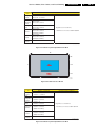
PDP Overviews
Table 1-1 PDP overview
PDP Type / Version
Model Name
H x V Pixel
1
42” SD v5
S42SD-YD09
852 x 480
2
42” HD w1
S42AX-YD02
1024 x 768
3
50” HD w1
S50HW-YD01
1366 x 768
4
63” HD v4
S63HW-XD05
1366 x 768
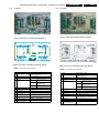
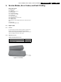
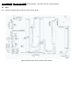
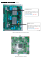
G_16380_001.eps
190606
Figure 1-1 Rear view of plasma panel (42” SD v5)
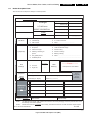
Table 1-2 PDP vs Chassis overview
Display type
42" SD v5
42" SD v5
42" HD w1
42" HD w1
50" HD w1
50" HD w1
63" HD v4
Model #
42PF5521D/10
42PF5521D/12
42PF9431D/37
42PF9631D/37
50PF9631D/37
50PF9731D/37
63PF9631D/37
Chassis
LC4.41E AB
LC4.41E AB
BJ2.5U PA
BJ2.4U PA
BJ2.4U PA
BJ2.4U PA
BJ3.0U PA
Chassis Manual #
3122 785 16230
3122 785 16230
3122 785 15930
3122 785 15920
3122 785 15920
3122 785 15920
3122 785 16460
In above table the link is given between the SDI Plasma Display
Panel and the Philips TV chassis (incl. chassis manual no.).
G_16380_002.eps
190606
Figure 1-2 Location of mounting screws (42” SD v5)
NOTE: screw torque 9.5 ± 0.5 kgf.cm
No
Item
Specification 42” SD v5
1
Pixel
852 (H) x 480 (V) pixels
(1 pixel = 1 R,G,B cells)
2
Number of Cells
2556 (H) x 480 (V)
3
Pixel Pitch
1.095 (H) mm x 1.110 (V) mm
4
Cell Pitch
R
0.365 (H) mm x 1.110 (V) mm
G
0.365 (H) mm x 1.110 (V) mm
B
0.365 (H) mm x 1.110 (V) mm
5
Display size
932.940 (H) x 532.800 (V) mm
6
Screen size
Diagonal 42" Colour Plasma Display Module
7
Screen aspect
16:9
8
Display colour
16.77 million colours (8-bit)
9
Viewing angle
Over 160 deg (angle with 50% and greater brightness
perpendicular to PDP module)
10
Dimensions
982 (W) x 582 (H) x 54 (D) mm
11
Weight
1 Module
14
Vertical frequency
60 Hz/ 50 Hz, LVDS
and
Video/Logic Interface
About 15.4 kg
Technical Specifications, Connections, and Chassis Overview
1.1.2
42" HD w1
1.1.3
SDI PDP 2K6
1.
50" HD w1
G_16380_005.eps
190606
G_16380_003.eps
190606
Figure 1-3 Rear view of plasma panel (42” HD w1)
Figure 1-5 Rear view of plasma panel (50” HD w1)
G_16380_004.eps
190606
Figure 1-4 Location of mounting screws (42” HD w1)
NOTE: screw torque 9.5 ± 0.5 kgf.cm
EN 3
G_16380_006.eps
190606
Figure 1-6 Location of mounting screws (50” HD w1)
NOTE: screw torque 9.5 ± 0.5 kgf.cm
No
Item
Specification 42” HD w1
1
Pixel
1.024 (H) x 768 (V) pixels
(1 pixel = 1 R,G,B cells)
2
Number of Cells
3072 (H) x 768 (V)
3
Pixel Pitch
0.912mm (H) x 0.693mm (V)
4
Cell Pitch
R
Horizontal 0.304 mm
Vertical 0.693 mm
No
Item
Specification 50” HD w1
1
Pixel
1366 (H) x 768 (V) pixels
(1 pixel = 1 R,G,B cells)
2
Number of Cells
4,098 (H) x 768 (V) cells
3
Pixel Pitch
0.810 mm (H) x 0.810 mm (V)
4
Cell Pitch
R
Horizontal 0.270 mm
Vertical 0.810 mm
G
Horizontal 0.304 mm
Vertical 0.693 mm
G
B
Horizontal 0.304 mm
Vertical 0.693 mm
Horizontal 0.270 mm
Vertical 0.810 mm
B
Horizontal 0.270 mm
Vertical 0.810 mm
5
Display size
933.89 (H) x 532.22 (V) mm
6
Screen size
Diagonal 42" Colour Plasma Display Module
5
Display size
1106.46 mm (H) x 622.08 mm (H)
7
Screen aspect
16:9
6
Screen size
Diagonal 50" Colour Plasma Display Module
8
Display colour
1073.7 million colours (10-bit)
7
Screen aspect
16:9
9
Viewing angle
Over 160 deg (angle with 50% and greater
brightness perpendicular to PDP module)
8
Display colour
549.75 billion colours (13-bit)
9
Viewing angle
Over 160 deg (angle with 50% and greater
brightness perpendicular to PDP module)
10
Dimensions
1175 (W) x 678.5 (H) x 63.8 (D) mm
11
Weight
Module 1
12
Vertical frequency
Video/Logic Interface
60/50 Hz, LVDS
10
Dimensions
982 (W) x 582 (H) x 54 (D) mm
11
Weight
1 Module
12
Vertical frequency
Video/Logic Interface
60/50 Hz, LVDS
About 16.8 kg
About 18.0 kg
EN 4
1.1.4
1.
Technical Specifications, Connections, and Chassis Overview
SDI PDP 2K6
1.2
63" HD v4
Serial Numbers
}G
zGuUG
G_16380_007.eps
190606
G_16380_035.eps
121006
Figure 1-7 Rear view of plasma panel (63” HD v4)
Figure 1-9 Location of the serial number
C
001 A
5 1 03 A
0
0
0
1
Serial No : 0001~9999
Shift : A = Day, B = Afternoon,
C = Night
Day: 01 ~ 31
Month : 1 ~ C
(Oct = A, Nov = B, Dec = C)
Year :
G_16380_036.eps
121006
Figure 1-8 Location of mounting screws (63” HD v4)
0 (2000) ~ 9 (2009)
Line No : A ~ Z
Type : 298 (42SDV5)
Type : 310 (42HDW1)
Type : 272 (50HDW1)
Type : 327 (63HDV4)
Factory: C [= Cheonan]
S [= Shenzen]
G_16380_008.eps
161006
NOTE: screw torque 9.5 ± 0.5 kgf.cm
Figure 1-10 Explanation of the serial number
No
Item
Specification 63” HD v4
1
Pixel
1366 (H) x 768 (V) pixels
(1 pixel = 1 R,G,B cells)
2
Number of Cells
4,098 (H) x 768 (V) cells
3
Pixel Pitch
1.02 mm (H) x 1.02 mm (V)
4
Cell Pitch
R
Horizontal 0.34 mm
Vertical 1.02 mm
G
Horizontal 0.34 mm
Vertical 1.02 mm
B
Horizontal 0.34 mm
Vertical 1.02 mm
5
Display size
6
Screen size
1393.3 mm (H) x 783.4 mm (H)
Diagonal 63" Colour Plasma Display Module
7
Screen aspect
16:9
8
Display colour
1073.7 million colours (13-bit)
9
Viewing angle
Over 160 deg (angle with 50% and greater
brightness perpendicular to PDP module)
10
Dimensions
approx. 1680 (W) x 875 (H) x 750 (D) mm
11
Weight
Module 3
12
Vertical frequency
Video/Logic Interface
60/50 Hz, LVDS
About 44.0 kg
Technical Specifications, Connections, and Chassis Overview
1.3
Chassis Overviews
1.3.1
42” SD v5
SDI PDP 2K6
1.
EN 5
^G
X
X\G
[G
ZG
X]
Y
\G
XZG
_G
XW
]
XY
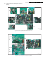
XX
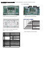
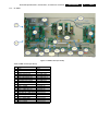
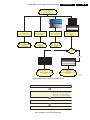
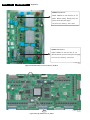
Figure 1-11 PWB location (42” SD v5)
Table 1-3 PWB overview (42” SD v5)
No.
1
2
3
4
5
6
7
8
9
10
11
12
13
14
15
16
Location
SMPS
LOGIC-MAIN Board
X-MAIN Driving Board
Y-MAIN Driving Board
LOGIC E BUFFER Board
LOGIC F BUFFER Board
Y-BUFFER Board
LOGIC + Y-MAIN
LOGIC + X-MAIN
LOGIC + LOGIC BUF (E)
LOGIC + LOGIC BUF (F)
LOGIC BUF (E) + (F)
SMPS + LOGIC BUF (E)
SMPS + LOGIC MAIN
SMPS + Y-MAIN
SMPS + X-MAIN
Name
SMPS
Assy PWB Logic Main
Assy PWB X Main
Assy PWB Y Main
Assy PWB buffer
Assy PWB buffer
Assy PWB buffer
Lead connector
Lead connector
FFC cable-flat
FFC cable-flat
Lead connector
Lead connector
Lead connector
Lead connector
Lead connector
X[
`G
G_16380_009.eps
190606
EN 6
1.3.2
1.
Technical Specifications, Connections, and Chassis Overview
SDI PDP 2K6
42” HD w1
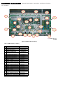
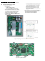
^G
X
X]
X\G
ZG
[G
Y
XZ
]
\G
XY
XW
_G
XX
Figure 1-12 PWB location (42” HD w1)
Table 1-4 PWB overview (42” HD w1)
No.
1
2
3
4
5
6
7
8
9
10
11
12
13
14
15
16
Location
SMPS
LOGIC-MAIN Board
X-MAIN Driving Board
Y-MAIN Driving Board
LOGIC E BUFFER Board
LOGIC F BUFFER Board
Y-BUFFER Board
LOGIC + Y-MAIN
LOGIC + X-MAIN
LOGIC + LOGIC BUF(E)
LOGIC + LOGIC BUF(F)
LOGIC BUF(E) + LOG. BUF(F)
SMPS + LOGIC BUF(E)
SMPS + LOGIC MAIN
SMPS + Y-MAIN
SMPS + X-MAIN
Name
SMPS
Assy PWB LOGIC Main
Assy PWB X Main
Assy PWB Y Main
Assy PWB Buffer
Assy PWB Buffer
Assy PWB Buffer
Lead connector
Lead connector
FFC Cable-flat
FFC Cable-flat
Lead connector
Lead connector
Lead connector
Lead connector
Lead connector
`G
X[
G_16380_010.eps
190606
Technical Specifications, Connections, and Chassis Overview
1.3.3
SDI PDP 2K6
1.
EN 7
50” HD w1
YW
X`
_G
X
[G
ZG
X_
Y
`G
\G
X^
XY
XW
XZ
X[
]
X\G
X]
^G
XX
G_16380_011.eps
190606
Figure 1-13 PWB location (50” HD w5)
Table 1-5 PWB overview (50” HD w1)
No.
1
2
3
4
5
6
7
8
9
10
11
12
13
14
15
16
17
18
19
20
Location
SMPS
LOGIC-MAIN Board
X-MAIN Driving Board
Y-MAIN Driving Board
LOGIC E BUFFER Board
LOGIC F BUFFER Board
LOGIC G BUFFER Board
Y-BUFFER (Upper) Board
Y-BUFFER (Lower) Board
LOGIC + Y-MAIN
LOGIC + X-MAIN
LOGIC + LOGIC BUF (E)
LOGIC + LOGIC BUF (F)
LOGIC + LOGIC BUF (G)
LOGIC BUF (E) + LOG. BUF (F)
LOGIC BUF (F) + LOG. BUF (G)
SMPS + LOGIC BUF (E)
SMPS + LOGIC MAIN
SMPS + Y-MAIN
SMPS + X-MAIN
Name
SMPS
Assy PWB LOGIC Main
Assy PWB X Main
Assy PWB Y Main
Assy PWB Buffer E
Assy PWB Buffer F
Assy PWB Buffer G
Assy PWB Buffer
Assy PWB Buffer
FFC Cable-flat
FFC Cable-flat
FFC Cable-flat
FFC Cable-flat
FFC Cable-flat
Lead connector
Lead connector
Lead connector
Lead connector
Lead connector
Lead connector
EN 8
1.3.4
1.
Technical Specifications, Connections, and Chassis Overview
SDI PDP 2K6
63” HD v4
Y]G
Y\
YZG
_G
XW
YYG
X]G
YW
X
X\
[G
ZG
YXG
`G
X`
Y
Y[G
XX
X[
XYG
\G
X^
X_
]
XZ
^G
G_16380_037.eps
121006
Figure 1-14 PWB location (63” HD v4)
Table 1-6 PWB overview (50” HD w1)
No.
1
2
3
4
5
6
7
8
9
10
11
12
13
14
15
16
17
18
19
20
21
22
23
24
25
26
Location
SMPS
LOGIC-MAIN Board
X-MAIN Driving Board
Y-MAIN Driving Board
LOGIC E BUFFER Board
LOGIC F BUFFER Board
LOGIC G BUFFER Board
Y-BUFFER (Upper) Board
Y-BUFFER (Lower) Board
X-BUFFER (Upper) Board
X-BUFFER (Lower) Board
LOGIC + Y-MAIN
LOGIC + X-MAIN
LOGIC + LOGIC BUF upper (E)
LOGIC + LOGIC BUF upper (F)
LOGIC + LOGIC BUF upper (G)
LOGIC + LOGIC BUF lower (E)
LOGIC + LOGIC BUF lower (F)
LOGIC + LOGIC BUF lower (G)
SMPS + LOGIC MAIN
SMPS + Y-MAIN
SMPS + X-MAIN
SMPS + LOGIC BUF upper (E)
SMPS + LOGIC BUF lower (E)
LOGIC BUF (E) + LOG. BUF (F)
LOGIC BUF (F) + LOG. BUF (G)
Name
SMPS
Assy PWB LOGIC Main
Assy PWB X Main
Assy PWB Y Main
Assy PWB Buffer E
Assy PWB Buffer F
Assy PWB Buffer G
Assy PWB Buffer
Assy PWB Buffer
Assy PWB Buffer
Assy PWB Buffer
FFC Cable-flat
FFC Cable-flat
FFC Cable-flat
FFC Cable-flat
FFC Cable-flat
FFC Cable-flat
FFC Cable-flat
FFC Cable-flat
Lead connector
Lead connector
Lead connector
Lead connector
Lead connector
Lead connector
Lead connector
Safety Instructions, Warnings, and Notes
SDI PDP 2K6
2.
EN 9
2. Safety Instructions, Warnings, and Notes
Index of this chapter:
2.1 Handling Precautions
2.2 Safety Precautions
2.3 Notes
Notes:
• Only authorised persons should perform servicing of this
module.
• When using/handling this unit, pay special attention to the
PDP Module: it should not be enforced into any other way
then next rules, warnings, and/or cautions.
• "Warning" indicates a hazard that may lead to death or
injury if the warning is ignored and the product is handled
incorrectly.
• "Caution" indicates a hazard that can lead to injury or
damage to property if the caution is ignored and the
product is handled incorrectly.
2.1
•
•
•
2.2.2
•
•
•
•
The PDP module use high voltage that is dangerous to
humans. Before operating the PDP, always check for dust
to prevent short circuits. Be careful touching the circuit
device when power is “on”.
The PDP module is sensitive to dust and humidity.
Therefore, assembling and disassembling must be done in
no dust place.
The PDP module has a lot of electric devices. The service
engineer must wear equipment (for example, earth ring) to
prevent electric shock and working clothes to prevent
electrostatic.
The PDP module use a fine pitch connector which is only
working by exactly connecting with flat cable. The operator
must pay attention to a complete connection when
connector is reconnected after repairing.
The capacitor’s remaining voltage in the PDP module’s
circuit board temporarily remains after power is “off”.
Operator must wait for discharging of remaining voltage
during at least 1 minute.
2.2
Safety Precautions
2.2.1
Safety Precautions
•
•
•
•
•
•
•
•
•
•
Before replacing a board, discharge forcibly the remaining
electricity from the board.
When connecting FFC and TCPs to the module, recheck
that they are perfectly connected.
To prevent electrical shock, be careful not to touch leads
during circuit operations.
To prevent the Logic circuit from being damaged due to
wrong working, do not connect/disconnect signal cables
during circuit operations.
Do thoroughly adjustment of a voltage label and voltageinsulation.
Before reinstalling the chassis and the chassis assembly,
be sure to use all protective stuff including a nonmetal
controlling handle and the covering of partitioning type.
Caution for design change: Do not install any additional
devices to the module, and do not change the electrical
circuit design.
For example: Do not insert a subsidiary audio or video
connector. If you insert It, it cause danger on safety. And, if
you change the design or insert, manufacturer guarantee
will be not effect.
If any parts of wire is overheats of damaged, replace it with
a new specified one immediately, and identify the cause of
the problem and remove the possible dangerous factors.
Examine carefully the cable status if it is twisted or
damaged or displaced. Do not change the space between
ESD Precautions
There are parts, which are easily damaged by electrostatics
(for example Integrated Circuits, FETs, etc.) Electrostatic
damage rate of product will be reduced by the following
technics:
• Before handling semiconductor parts/assembly, must
remove positive electric by ground connection, or must
wear the antistatic wrist-belt and ring (it must be operated
after removing dust on it. It comes under precaution of
electric shock).
• After removing the assembly, lay it with the tracks on a
conductive surface to prevent charging.
• Do not use chemical stuff containing Freon. It generates
positive electric that can damage ESD sensitive devices.
• You must use a soldering device for ground-tip when
soldering or de-soldering these devices.
• You must use anti-static solder removal device. Most
removal devices do not have antistatic which can charge a
enough positive electric enough for damaging these
devices.
• Before removing the protective material from the lead of a
new device, bring the protective material into contact with
the chassis or assembly.
• When handing an unpacked device for replacement, do not
move around too much. Moving (legs on the carpet, for
example) generates enough electrostatic to damage the
device.
• Do not take a new device from the protective case until the
it is ready to be installed. Most devices have a lead, which
is easily short-circuited by conductive materials (such as
conductive foam and aluminium)
Handling Precautions
•
parts and circuit board. Check the cord of AC power
preparing damage.
Product Safety Mark: Some of electric or implement
material have special characteristics invisible that was
related on safety. In case of the parts are changed with new
one, even though the Voltage and Watt is higher than
before, the Safety and Protection function will be lost.
The AC power always should be turned “off”, before next
repair.
Check assembly condition of screw, parts and wire
arrangement after repairing. Check whether the material
around the parts get damaged.
2.3
Notes
A glass plate is positioned before the plasma display. This
glass plate can be cleaned with a slightly humid cloth. If due to
circumstances there is some dirt between the glass plate and
the plasma display panel, it is recommended to do some
maintenance by a qualified service employee only.
2.3.1
Safe PDP Handling
•
•
•
•
The work procedures shown with the “Note” indication are
important for ensuring the safety of the product and the
servicing work. Be sure to follow these instructions.
Before starting the work, secure a sufficient working space.
At all times, other than when adjusting and checking the
product, be sure to turn “off” the main POWER switch and
disconnect the power cable from the power source of the
display (jig or the display itself) during servicing.
To prevent electric shock and breakage of PWBs, start the
servicing work at least 30 seconds after the main power
has been turned “off”. Especially when installing and
removing the Power Supply PWB and the SUS PWB in
which high voltages are applied, start servicing at least 2
minutes after the main power has been turned “off”.
EN 10
•
•
•
•
•
3.
SDI PDP 2K6
Directions For Use
While the main power is “on”, do not touch any parts or
circuits other than the ones specified. The high voltage
Power Supply block within the PDP module has a floating
ground. If any connection other than the one specified is
made between the measuring equipment and the high
voltage power supply block, it can result in electric shock or
activation of the leakage-detection circuit breaker.
When installing the PDP module in, and removing it from
the packing carton, be sure to have at least two persons
perform the work while being careful to ensure that the
flexible printed-circuit cable of the PDP module does not
get caught by the packing carton.
When the surface of the panel comes into contact with the
cushioning materials, be sure to confirm that there is no
foreign matter on top of the cushioning materials before the
surface of the panel comes into contact with the cushioning
materials. Failure to observe this precaution may result in,
the surface of the panel being scratched by foreign matter.
When handling the circuit PWB, be sure to remove static
electricity from your body before handling the circuit PWB.
Be sure to handle the circuit PWB by holding the large parts
as the heat sink or transformer. Failure to observe this
3. Directions For Use
Not applicable.
•
•
•
precaution may result in the occurrence of an abnormality
in the soldered areas.
Do not stack the circuit PWB. Failure to observe this
precaution may result in problems resulting from scratches
on the parts, the deformation of parts, and short-circuits
due to residual electric charge.
Routing of the wires and fixing them in position must be
done in accordance with the original routing and fixing
configuration when servicing is completed. All the wires are
routed far away from the areas that become hot (such as
the heat sink). These wires are fixed in position with the
wire clamps so that the wires do not move, thereby
ensuring that they are not damaged and their materials do
not deteriorate over long periods of time. Therefore, route
the cables and fix the cables to the original position and
states using the wire clamps.
Perform a safety check when servicing is completed. Verify
that the peripherals of the serviced points have not
undergone any deterioration during servicing. Also verify
that the screws, parts and cables removed for servicing
purposes have all been returned to their proper locations in
accordance with the original
Mechanical Instructions
SDI PDP 2K6
4.
EN 11
4. Mechanical Instructions
Index of this chapter:
4.1 Dis-assembling / Re-assembling
4.1.1 Flexible Printed Circuit of Y-Buffer (Upper and Lower)
4.1.2 Flat Cable Connector of X-main Board
4.1.3 FFC and TCP from Connector
4.1.4 Exchange of LBE and LBF board - 42” SD v5
4.1.5 Exchange of LBE and LBF board - 42” HD w1
4.1.6 Exchange of LBE, LBF and LBG board - 50” HD w1
4.1.7 Exchange of LB-E, LB-F and LB-G board - 63” HD v4
4.1.8 Exchange YB and YM board - 42” SD v5
4.1.9 Exchange YB and YM board - 42” HD w1
4.1.10 Exchange YBU, YBL and YM board - 50” HD w1
4.1.11 Exchange YBU, YBL and YM board - 63” HD v4
4.1
Dis-assembling / Re-assembling
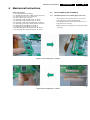
4.1.1
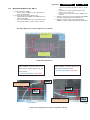
Flexible Printed Circuit of Y-Buffer (Upper and Lower)
•
•
Dis-assembly: Pull out the FPC from the connector by
holding the lead of the FPC with both hands.
Re-assembly: Push the lead of FPC with same force on
both sides into the connector.
Note: Be careful not to damage the connector pin during
connecting.
G_16380_012.eps
190606
Figure 4-1 Dis-assembly FPC of Y-buffer
G_16380_013.eps
190606
Figure 4-2 Re-assembly FPC of Y-buffer
EN 12
4.1.2
4.
SDI PDP 2K6
Mechanical Instructions
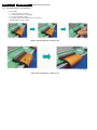
Flat Cable Connector of X-main Board
•
•
Dis-assembly:
1. Pull out the clamp of connector.
2. Pull Flat cable out press down lightly.
3. Turn the Flat Cable reversely.
Re-assembly: Put the Flat Cable into the connector press
down lightly until you hear a “Click“.
G_16380_014.eps
190606
Figure 4-3 Dis-assembly FCC of X-main board
G_16380_015.eps
190606
Figure 4-4 Re-assembly FCC of X-main board
Mechanical Instructions
4.1.3
SDI PDP 2K6
4.
EN 13
FFC and TCP from Connector
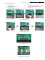
•
•
Dis-assembling of TCP:
1. Open the clamp carefully.
2. Pull the TCP out from its connector.
Re-assembling of TCP:
1. Put the TCP into the connector carefully
2. Close the clamp completely, until you hear a “Click”.
Notes:
• Checking whether the foreign material is on the connector
inside before assembling of TCP.
• Be careful, do not damage the board by ESD during
handling of TCP.
G_16380_016.eps
190606
Figure 4-5 Dis-assembly of TCP
G_16380_017.eps
190606
Figure 4-6 Re-assembly of TCP
G_16380_018.eps
190606
Figure 4-7 Mis-assembly of TCP
G_16380_019.eps
190606
Figure 4-8 Dis- and re-assembly of FFC
EN 14
4.1.4
4.
SDI PDP 2K6
Mechanical Instructions
6. Clean the connectors.
7. Re-connect the TCP, FFC, and the power cable to the
connectors.
8. Re-assemble the TCP heat sink. Use the screw mounting
order 2-3-1.
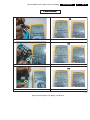
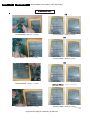
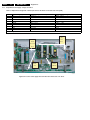
Exchange of LBE and LBF board - 42” SD v5
1. Remove the screws in order of 1-3-2 from the heatsink and
remove the heatsink (“Photos 1 & 3”)
2. Remove the TPC, FFC, and the power cable from the
connectors.
3. Remove all the screws from the defective board (“Photo
2”).
4. Remove the defective board.
5. Place the new board and screw it tight.
1
Caution: If you screw too tight, it is possible to damage the
Driver IC of the TCP.
2
3
G_16380_020.eps
160606
Figure 4-9 Photo 1 - Heatsink 42” SD v5
G_16380_021.eps
160606
Figure 4-10 Photo 2 - Exchange of LBE and LBF board 42” SD v5
G_16380_022.eps
160606
Figure 4-11 Photo 3 - Heat sink removal
Mechanical Instructions
4.1.5
4.
EN 15
6. Clean the connectors.
7. Re-connect the TCP, FFC, and power cable to the
connectors.
8. Re-assemble the TCP heat sink. Use the screw mounting
order 2-1-3.
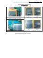
Exchange of LBE and LBF board - 42” HD w1
1. Remove the screws in order of 1-3-2 from the heatsink and
remove the heatsink (“Photos 1 & 3”).
2. Remove the TPC, FFC, and power cable from the
connectors.
3. Remove all the screws from the defective board.
4. Remove the defective board.
5. Place the new board and then screw tightly.
1
SDI PDP 2K6
Caution: If you screw too tight, it is possible to damage the
Driver IC of the TCP.
2
3
G_16380_027.eps
160606
Figure 4-12 Photo 1 - Heatsink 42” HD w1
G_16380_024.eps
160606
Figure 4-13 Photo 2 - Exchange of LBE, LBF board 42” HD w1
G_16380_022.eps
160606
Figure 4-14 Photo 3 - Heat sink removal
EN 16
4.1.6
4.
SDI PDP 2K6
Mechanical Instructions
Exchange of LBE, LBF and LBG board - 50” HD w1
1. Remove the screws in order of 2-3-1-4 from the heatsink
and remove the heatsink (“Photo 3”).
2. Remove the TPC, FFC, and power cable from the
connectors.
3. Remove all the screws from the defective board.
4. Remove the defective board.
5. Replace the new board and then screw tightly.
1
2
6. Clean the connectors.
7. Re-connect the TCP, FFC, and power cable to the
connectors.
8. Re-assemble the TCP heat sink. Use the same screw
mounting order as described above
Caution: If you screw too tight, it is possible to damage the
Driver IC of the TCP.
3
4
G_16380_023.eps
160606
Figure 4-15 Photo 1 - Heatsink 50” HD w1
G_16380_026.eps
160606
Figure 4-16 Photo 2 - Exchange of LBE, LBF, LBG board 50” HD w1
G_16380_022.eps
160606
Figure 4-17 Photo 3 - Heat sink removal
Mechanical Instructions
4.1.7
SDI PDP 2K6
4.
EN 17
3. Remove the fixation screws [5] from the TPC heatsinks of
the defective board.
4. Unplug the TPC, FFC, and power cable(s) from the
connectors [6].
5. Remove the fixation screws from the defective board [7].
6. Remove the defective board.
7. Replace the new board and then screw tightly.
8. Clean the connectors.
9. Re-connect the TCP, FFC, and power cable to the
connectors.
10. Re-assemble the TCP heat sinks. Slide the heatsink
against strip [8] before you tighten it.
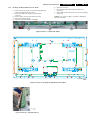
Exchange of LB-E, LB-F and LB-G board - 63” HD v4
1. Refer to the Service Manual of the set to strip it so far, you
have access to the Logic Buffer board that you need to
replace.
2. For the lower LB-E, remove brackets [1] and [2]; for the
lower LB-G, remove brackets [3] and [4]. For both LB-F’s
and the upper LB-E and LB-G you do not need to remove
these brackets.
Note: The following description is correct for the lower
LBG; the replacement procedure of the other LB’s is
similar.
1
3
2
4
G_16380_038.eps
131006
Figure 4-18 Brackets 63” HD v4
7
7
8
6
7
6
7
7
5
5
G_16380_039.eps
131006
Figure 4-19 Exchange of lower LB-G board 63” HD v4
EN 18
4.1.8
4.
SDI PDP 2K6
Mechanical Instructions
Exchange YB and YM board - 42” SD v5
1. Unplug all of the FPC connectors of Y-Buffer. See “Photo
1”.
2. Unplug connectors CN5001 and CN5008 from YMain. See “Photo 2”.
3. Loosen all the screws of Y-Buffer and Y-Main. See “Photo
3”.
4. Remove the board from the chassis.
5. Unplug connectors CN5003, CN5004 and CN5005
between Y-Buffer and Y-Main.
6.
7.
8.
9.
10.
11.
12.
13.
Remove Y-Buffer from Y-main.
Replace the defective board.
Re-assemble Y-Buffer and Y-Main.
Plug in connectors CN5003, CN5004 and CN5005
between Y-Buffer and Y-Main. See “Photo 4”.
Arrange the boards on the chassis and tighten them.
Connect the FPC connectors. See “Photo 5”.
Supply the electric power to the module and then check the
waveform of the board.
Turn “off” the power after the waveform is adjusted.
G_16380_030.eps
190606
Figure 4-20 Photo 1 and 2: Dis-assembly of YB and YM - 42” SD v5
G_16380_031.eps
190606
Figure 4-21 Photo 3 and 4: Re-assembly of YB and YM - 42” SD v5
4.1.9
Exchange YB and YM board - 42” HD w1
1. Unplug all of the FPC connectors of Y-Buffer. See “Photo
1”.
2. Loosen all the screws of Y-Buffer and Y-Main. See “Photo
3”.
3. Remove the board from the chassis.
4. Unplug connectors CN5004, CN5011 and CN5012
between Y-Buffer and Y-Main.
5. Remove Y-Buffer from Y-main.
6. Replace the defective board.
7. Re-assemble Y-Buffer and Y-Main.
8. Plug in connectors CN5004, CN5011 and CN5012
between Y-Buffer and Y-Main. See “Photo 4”.
9. Arrange the boards on the chassis and tighten them.
10. Connect the FPC connectors.
11. Supply the electric power to the module and then check the
waveform of the board.
12. Turn “off” the power after the waveform is adjusted.
G_16380_032.eps
190606
Figure 4-22 Photo 1 and 2: Dis-assembly of YBU, YBL, and YM - 42” HD w1
Mechanical Instructions
4.1.10 Exchange YBU, YBL and YM board - 50” HD w1
1. Unplug all of the FPC connectors of YBU (Y-Buffer upper)
and YBL (Y-Buffer lower). See “Photo 1”.
2. Unplug the connector CN5412 between YBU and YBL.
3. Loosen all the screws of YBU, YBL, and Y-Main.
4. Remove the board from the chassis.
5. Remove the YBL and YBU from Y-main.
6. Replace the defective board.
SDI PDP 2K6
4.
EN 19
7.
8.
9.
10.
11.
Re-assemble the YBU and YBL to the Y-Main.
Plug in connector CN5412 between YBU and YBL.
Arrange the board on the chassis and then screw to fix.
Connect the FPCs.
Supply the electric power to the module and then check the
waveform of the board.
12. Turn “off” the power after the waveform is adjusted.
G_16380_033.eps
190606
Figure 4-23 Photo 1 and 2: Dis-assembly of YBU, YBL, and YM - 50” HD w1
G_16380_034.eps
190606
Figure 4-24 Photo 3 and 4: Re-assembly of YBU, YBL, and YM - 50” HD w1
EN 20
4.
SDI PDP 2K6
Mechanical Instructions
4.1.11 Exchange YBU, YBL and YM board - 63” HD v4
1. Unplug power connector CN5010 and signal connector
CN5002 from Y-Main. See “Photo 1”.
2. Unplug all FPC connectors of YBU (Y-Buffer upper) and
YBL (Y-Buffer lower). See “Photo 1”.
3. Open the connectors CN5001/CN5406 between YM and
YBU, and CN5000/CN5506 between YM and YBL.
4. Loosen all the screws of YBU, YBL, and Y-Main.
5. Remove the boards from the chassis.
6. Open the connectors CN5410/CN5510 between YBU and
YBL.
7. Separate the YBL and YBU from Y-main.
8. Replace the defective board.
9. Re-assemble the YBU and YBL to the Y-Main.
10. Plug in the connectors between YBU, YBL and YM.
11. Arrange the board on the chassis and then screw to fix.
12. Reconnect the FPCs.
13. Supply the electric power to the module and then check the
waveform of the board.
14. Turn “OFF” the power after the waveform is adjusted.
Make sure you open these
connectors before you
separate the boards !
G_16380_042.eps
161006
Figure 4-25 Photo 1: Dis-assembly of YBU, YBL, and YM - 63” HD v4
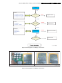
Service Modes, Error Codes, and Fault Finding
SDI PDP 2K6
5. Service Modes, Error Codes, and Fault Finding
Index of this chapter:
5.1 Repair Tools
5.1.1 ComPair
5.1.2 Other Service Tools
5.2 Fault Finding
5.2.1 Possible Scenarios
5.2.2 Faulty Power Supply
5.2.3 No Display
5.2.4 Abnormal display
5.2.5 Horizontal line or block open
5.2.6 Address open
5.2.7 Address short
5.2.8 Criteria for Panel Replacement, due to Defective Panel
Cells
5.2.9 Overview
5.3 Defect Description Form
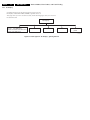
5.1
Repair Tools
5.1.1
ComPair
For the v5 and w1 models, it will be possible to generate test
patterns with ComPair. The ComPair interface must be
connected to the Logic Board with the special interconnection
cable (see table below for the order code).
5.1.2
Other Service Tools
Table 5-1 Overview Service tools
Service Tools
ComPair / SDI interconnection cable
Foam buffers (2 pcs.)
Order Code
3122 785 90800
3122 785 90581
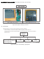
G_16380_029.eps
160606
Figure 5-1 Foam buffers
5.
EN 21
EN 22
5.
SDI PDP 2K6
5.2
Fault Finding
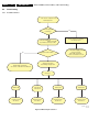
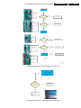
5.2.1
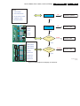
Possible Scenarios
Service Modes, Error Codes, and Fault Finding
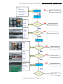
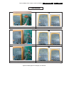
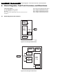
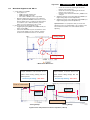
First check complete TV set.
Fault Symptom?
Power Supply
is working ?
No
Check if LVDS from
SSB board is OK.
Use LVDS Tool when possible.
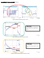
Go to “Power Supply Check”
& repair scenario
with Philips application
or PDP as stand alone check.
Output of SSB is OK?
No
Power supply is not working.
No voltage output.
SDI repair Scenario.
Fault finding: Display fault.
Repair Philips application.
See chassis related Service Manuals
Chassis ?
LC4.41E AB
BJ2.4U PA
BJ2.4U PA
BJ3.0U PA
Repair Scenario
50” HD w1
Repair Scenario
63” HD v4
BJ2.5U PA
Repair Scenario
42” SD v5
Repair Scenario
42” HD w1
G_16380_120.eps
161006
Figure 5-2 Which repair scenario?
Service Modes, Error Codes, and Fault Finding
SDI PDP 2K6
5.
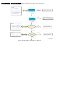
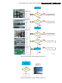
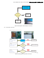
First check complete TV set.
Fault Symptom?
No Voltage output
Operating Voltages don´t exist
Go to
“Power Supply Check”
flowchart
(version dependent)
Operating Voltages exist,
but No Display
Some horizontal or Vertical
Lines don´t exist on the
Display.
Sustain open
Abnormal Display, not
open or short Lines
Go to
Go to the
“No Display”
“Abnormal Display”
flowchart
flowchart
Horizontal or
Vertical Lines?
Vertical
Horizontal
Is related to Logic adress Buffer.
Go to “Address
Open / Short”
flowchart
Is related to X-Main, Y-Main
and Y-buffer.
Go to “Sustain Open / Short”
flowchart
G_16380_056.eps
160606
Figure 5-3 Fault symptom overview (complete TV set)
XUGjGG GGGG G G
YUGjGGGsGGGG[YˉzkG\aGGslkGYWWWG
GGGGGG[YˉokGXaGslkGYWXXG
GGGGGG\WˉokGXaGslkGYWWYG
GGGGGG]ZˉokG[aGGslkGYWWYG G
ZUGjVGGGGGG
G
[UGjGGGGGG
G_16380_122.eps
161006
Figure 5-4 Repair scenario stand alone panels
EN 23
EN 24
5.2.2
5.
Service Modes, Error Codes, and Fault Finding
SDI PDP 2K6
Faulty Power Supply
NO
Reconnect it
AC Input
Check CN8001/2pin
Connect [220V ac]
YES
Check
1 SMPS
O
NO
SMPS Voltage check
D5V: 5V
Check
LED 8001,8002
Vs: 207V
Check
Green
Va:
65V
Check
Vset: 201V
Check
Vscan: -190V
Check
Ve: 110V
Check
Vcc: 15V
Check
D3V3: 3.3V
Check
5Vstandby: 5.2V Check
Fuse
8001/8002/8005/8007
Replace SMPS
G_16380_123.eps
190606
Figure 5-5 Power Supply Check for 42” SD v5 models 1/2
On/OFF Relay
NO
(RLY 8001, 8002
SMPS
Acts?
LED (Green)
Replace
8001, 8002 off
SMPS
YES
Check Protection,
LED 8004(RED) is
1 Open CN 8001
O
NO
SMPS
Check
Until LED 8004 OFF,
OFF?
NO
Vs_on
Then Reset SMPS
If LED8004 is ON
Under voltage
Checking, repeat
1
O
YES
YES
Check output voltage
Vs, Va, Vset, Vscan, Ve
NO
Turn off Relay SW
=> Open these connector
One by One
-
CN8002, X-Main check
-
CN8003, Y-Main check
- CN8005/CN8006 Buffer check
Replace
Check output voltage
NO
Vs, Va, Vset, Vscan, Ve
Replace SMPS
YES
Go to 5.2.3 No Display
Figure 5-6 Power Supply Check for 42” SD v5 models 2/2
G_16380_123a.eps
190606
Service Modes, Error Codes, and Fault Finding
AC Input
SDI PDP 2K6
NO
5.
EN 25
Reconnect it
Check CN8001/2pin
Connect [ 220Vac]
YES
SMPS Voltage check
Check
NO
D5V: 5V
Check
LED 8001,8002
Vs: 195V
Check
Green
Va:
O SMPS
1
65V
Check
Vset: 190V
Check
Vscan: -190V
Check
Ve: 110V
Check
Vcc: 15V
Check
D3V3: 3.3V
Check
5Vstandby: 5.2V Check
Fuse
8001/8002/8005/8007
Replace SMPS
G_16380_124.eps
190606
Figure 5-7 Power Supply Check for 42” HD w1 models 1/2
On/OFF Relay
(RLY 8001, 8002
SMPS
NO
Acts?
LED (Green)
Replace
8001, 8002 off
SMPS
YES
Check Protection,
LED 8004(RED) is
SMPS
NO
1 Open CN 8001
O
Check
If LED 8004 is ON
Under voltage
Until LED 8004 OFF,
OFF?
NO
Vs_on
Checking, repeat
Then Reset SMPS
1
O
YES
YES
Check output voltage
Vs, Va, Vset, Vscan, Ve
NO
Turn off Relay SW
->
Open these connectors
-
CN8002, X-Main check
One by One
-
CN8003, Y-Main check
-
CN8005/CN8006 Buffer check
Replace SMPS
Check output voltage
NO
Vs, Va, Vset, Vscan
,Ve
Replace SMPS
YES
Go to 5.2.3 No Display
Figure 5-8 Power Supply Check for 42” HD w1 models 2/2
G_16380_124a.eps
190606
EN 26
5.
SDI PDP 2K6
Service Modes, Error Codes, and Fault Finding
NO
AC Input
Reconnect it
220Vac or 110Vac
Check CN1308
Connect [ 220Vac]
YES
SMPS Voltage check
NO
Check
1 SMPS
O
LED 8001,8002
D5V: 5V
Check
Vs: 202V
Check
Va:
Check
65V
Vset: 190V
Green
Check
Vscan: -190V
Check
Ve: 115V
Check
Vcc: 15V
Check
D3V3: 3.3V
Check
5Vstandby:59V Check
Fuse
F8001/8002/8005/8007
Replace SMPS
G_16380_125.eps
190606
Figure 5-9 Power Supply Check for 50” HD w1 models 1/2
NO
On/OFF Relay
(RLY 8001, 8002
SMPS
LED (Green)
Replace
8001, 8002 off
SMPS
Acts?
YES
NO
Check Protection,
LED 8004(RED) is
SMPS
1 Open CN 8001
O
If LED8004 is ON
Under voltage
Until LED 8004 OFF,
OFF?
NO
Check
Vs_on
1
Checking, repeat O
Then Reset SMPS
YES
YES
Check output voltage
Vs, Va, Vset, Vscan, Ve
NO
Turn off Relay SW
? Open these connector
One by One
-
CN8002, X-Main check
-
CN8003, Y-Main check
-
CN8005/CN8006
Buffer check
Replace
Check output voltage
NO
Vs, Va, Vset, Vscan
,V e
Replace SMPS
YES
Go to 5.2.3 No Display
Figure 5-10 Power Supply Check for 50” HD w1 models 2/2
G_16380_125a.eps
190606
Service Modes, Error Codes, and Fault Finding
SDI PDP 2K6
5.
NO
Ac Input
Reconnect it
230Vac or 120Vac
Check CN801
Connect [ 220Vac]
YES
SMPS Voltage check
NO
ྙSMPS
D5.3V;5Vsw
Check
Vs ; 184V
Check
Va ; 72V
Check
Vset; 178V
Check
Vscan; -160V
Check
Ve; 88V
Check
Vg; 15V
Check
D3V3; 8V6
Check
12Vssb;·Vsnd
[Note]
Check
5Vstb;
Do not Vs voltage occurrence
Check
Fuse ( F8101)
if there is no Vs _On signalG
Replace SMPS
G_16380_040.eps
161006
Figure 5-11 Power Supply Check for 63” HD v4 models 1/2
NO
ྙOn/OFF Relay
Insert Relay Switch at
-Turn Off Relay SW-
- Turn ON Relay SW-
Replace
SMPS
Discharge PFC Voltage
No PFC Voltage
SMPS
1M03
YES
at CN 804
NO
Check Protection
Use to Multi Meter at CN 804
Use to10W1kR
SMPS
ྚOpen CN 801
NO
Check
Then Reset SMPS
Vs on
Checking, repeat ྚ
(Use to10W1kR
YES
at CN 804)
YES
Check output voltage
Vs, Va, Vset, Vscan, Ve
NO
Turn off Relay SW
˧ Open these connector
One by One
-
CN804, X-Main check
-
CN805, Y-Main check
-
CN811/CN806
Buffer check
Replace
Check output voltage
NO
Vs, Va, Vset, Vscan
,V e
Replace SMPS
YES
Go to 4-1-2 No Display
Figure 5-12 Power Supply Check for 63” HD v4 models 2/2
G_16380_041.eps
161006
EN 27
EN 28
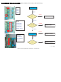
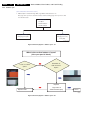
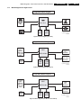
5.2.3
5.
SDI PDP 2K6
Service Modes, Error Codes, and Fault Finding
No Display
(operating voltage present, but an image doesn’t exist on Screen)
No Display is related with Y-MAIN, X-MAIN, Logic Main and so on.
This page shows you how to check the boards, and the following pages show you how to find
the defective board.
No Display
Logic Main
[42”SD: LED 2000 blinks;
42”HD and 50”HD: LED 2011 blinks
63”HD: LED 2002 blinks]
Y – Main
X – Main
Y – Buffer
Broken
panel
G_16380_127.eps
171006
Figure 5-13 Fault symptom: “No Display”, general guide line
Service Modes, Error Codes, and Fault Finding
SDI PDP 2K6
5.
EN 29
Check
LVDS Cable
LED 2000;Green
NO
Logic-main
Fuse F2000, F2001
Replace Logic Board
YES
CN803 Cable
Y-main
Check
F5001
F5003
Open
Fuse
Replace Y-Board
open?
Shor t
Check
Q5008
Q5009
Shor t
FET
Replace Y-Board
Q5010
Q5013
Open
Short?
X-main
Check
F4000
Open
F4003
open?
Fuse
Replace X-Board
Shor t
Check
Q4010
Q4011
Shor t
FET
Replace X-Board
Q4012
Q4015
Open
Short?
Shor t
Measure
Resistance
Y-buffer
Replace Y-buffer
OUTH&OUTL
Short?
Open
Panel
Replace PDP
G_16380_128.eps
190606
Figure 5-14 Fault symptom: “No Display”, 42” SD v5
EN 30
5.
SDI PDP 2K6
Service Modes, Error Codes, and Fault Finding
Check
ྙ LVDS Cable
ྚ LED 2010;Green
Logic-main
NO
Replace Logic Board
ྛ Fuse F2000, F2001
ྜ CN2026 Cable
YES
NO
Replace Logic Board
Y-main
YES
Check
ྙ F5001 for Vdd (5V)
ྚ F5004 for Vcc (15V)
Fuse
OPEN
Replace Y-Board
ྛ F5003 for Vs(200V)
Short
SHORT
Check
ྙ Q5009 ~ Q5021G
FET,IGBT
Replace Y-Board
Open
G_16380_129a.eps
190606
Figure 5-15 Fault symptom: “No Display”, 42” HD w1 1/7
Service Modes, Error Codes, and Fault Finding
SDI PDP 2K6
5.
EN 31
TGjGwG
vyG
Vs fuse (F5003) – OK (0.x ~ x.x ohm)
Vs fuse (F5003) – OPEN (x.x Mohm)
vyG
15V fuse (F5004) – OK (0.x ~ x.x ohm)
15V fuse (F5004) – OPEN (x.x Mohm)
vyG
5V fuse (F5001) – OK (0.x ~ x.x ohm)
5V fuse (F5001) – OPEN (x.x Mohm)
G_16380_129b.eps
190606
Figure 5-16 Fault symptom: “No Display”, 42” HD w1 2/7
EN 32
5.
SDI PDP 2K6
Service Modes, Error Codes, and Fault Finding
vyG
Vscan fuse (F5006) – OK (0.x ~ x.x ohm)
Vscan fuse (F5006) – OPEN (x.x Mohm)
pni{SGml{GjGwG
G
G
FET,IGBT (contain the inner diode)
[Ys, Yg, Ypn, Yscan, Yfr, Yrr, Xs, Xg, Xe)
OK
OK (0.3 ~ 0.9 V)
ShortG
/
Short (0.000 ~ 0.00x V)
G
OK
IGBT (do not contain the inner diode)
(Yr, Yf, Xr, Xf)
OK (xx.x kohm)
Short
/
Short (x.x ohm)
Ys(Q5013,14), Yg(Q5009,10), Ypn(Q5016,17,18), Yscan(Q5020,21), Yfr(Q5019), Yrr(Q5015),
Xs(Q4002,03), Xg(Q4011,12), Xe(Q4013,14)
Yr(Q5011), Yf(Q5012), Xr(Q4016), Xf(Q4015)G
G_16380_129c.eps
190606
Figure 5-17 Fault symptom: “No Display”, 42” HD w1 3/7
Service Modes, Error Codes, and Fault Finding
SDI PDP 2K6
5.
EN 33
X-main
YES
Check
ྙ F4004 for Vdd (5V)
ྚ F4001 for Vcc (15V)
OPEN
Fuse
Replace X-B’d
ྛ F4002 for Vs (200V)
SHORT
Check
SHORT
ྙ Q4002,3
FET,IGBT
Replace X-B’d
ྚ Q4011 ~ Q4016
OPEN
Measure
Resistance
Y-BUFFER
SHORT
Replace Y-BUFFER
OUTH&OUTL
Short?
OPEN
Replace PDP
Panel
TGjGwG
G_16380_129d.eps
190606
Figure 5-18 Fault symptom: “No Display”, 42” HD w1 4/7
vyG
Vs fuse (F4003) – OK (0.x ~ x.x ohm)
Vs fuse (F4003) – OPEN (x.x Mohm)
G_16380_129e.eps
190606
Figure 5-19 Fault symptom: “No Display”, 42” HD w1 5/7
EN 34
5.
SDI PDP 2K6
Service Modes, Error Codes, and Fault Finding
vyG
Ve fuse (F4005) – OK (0.x ~ x.x ohm)
Vs fuse (F4005) – OPEN (x.x Mohm)
vyG
15V fuse (F4001) – OK (0.x ~ x.x ohm)
Vs fuse (F4001) – OPEN (x.x Mohm)
vyG
5V fuse (F4004) – OK (0.x ~ x.x ohm)
5V fuse (F4004) – OPEN (x.x Mohm)
G_16380_129f.eps
190606
Figure 5-20 Fault symptom: “No Display”, 42” HD w1 6/7
Service Modes, Error Codes, and Fault Finding
SDI PDP 2K6
TGjGwG
OUTL<–>OUTH – OK (x.x Mohm)
OUTL<–>OUTH –Short (x.x ohm)
G_16380_129g.eps
190606
Figure 5-21 Fault symptom: “No Display”, 42” HD w1 7/7
Check
LVDS Cable
LED 2000;Green
Logic-main
NO
Replace Logic Board
Fuse F2000, F2002
CN8003 Cable
YES
LED2002 Blinks
NO
Replace Y-Board
Y-main
YES
Check
F5001
F5000
OPEN
Fuse
Replace Y-Board
F5003
Short
Check
U5009(IPM)
SHORT
FET,IPM
Replace Y-Board
U5010(IPM)
Q5002~7
Open
Q5009
G G G G G G G G G G G G G Q5012,13,
Q5027~30
G_16380_130.eps
190606
Figure 5-22 Fault symptom: “No Display”, 50” HD w1 1/6
5.
EN 35
EN 36
5.
SDI PDP 2K6
Service Modes, Error Codes, and Fault Finding
Y- main Check Point
OR
Vs fuse (F5003) – OK (0.x ~ x.x ohm)
Vs fuse (F5003) – OPEN (x.x Mohm)
OR
15V fuse (F5000) – OK (0.x ~ x.x ohm)
15V fuse (F5000) – OPEN (x.x Mohm)
OR
5V fuse (F5001) – OK (0.x ~ x.x ohm)
5V fuse (F5001) – OPEN (x.x Mohm)
G_16380_130a.eps
190606
Figure 5-23 Fault symptom: “No Display”, 50” HD w1 2/6
pni{SGml{GjGwG
G
OK
FET
[Ys, Yg, Ypn, Yscan, Yfr, Yrr, Xs, Xg, Xe)
OK (0.3 ~ 0.9 V)
ShortG
/
Short (0.000 ~ 0.00x V)
G_16380_130b.eps
190606
Figure 5-24 Fault symptom: “No Display”, 50” HD w1 3/6
Service Modes, Error Codes, and Fault Finding
SDI PDP 2K6
5.
EN 37
X-main
YES
Check
F4001
F4000
OPEN
Fuse
Replace X-Board
F4003
SHORT
Check
U4001(IPM)
SHORT
Replace X-Board
FET,IPM
U4002(IPM)
Q4000 ~ Q4001
OPEN
SHORT
Y-BUFFER
Replace Y-Buffer
Measure
Resistance
OPEN
OUTH&OUTL
Short?
Panel
Replace Y-Buffer
G_16380_130c.eps
190606
Figure 5-25 Fault symptom: “No Display”, 50” HD w1 4/6
EN 38
5.
SDI PDP 2K6
Service Modes, Error Codes, and Fault Finding
X- main Check Point
OR
Vs fuse (F4003) – OK (0.x ~ x.x ohm)
Vs fuse (F4003) – OPEN (x.x Mohm)
OR
15V fuse (F4000) – OK (0.x ~ x.x ohm)
Vs fuse (F4000) – OPEN (x.x Mohm)
OR
5V fuse (F4001) – OK (0.x ~ x.x ohm)
Vs fuse (F4001) – OPEN (x.x Mohm)
G_16380_130d.eps
190606
Figure 5-26 Fault symptom: “No Display”, 50” HD w1 5/6
TGjGwG
OUTL<–>OUTH – OK (x.x Mohm)
OUTL<–>OUTH –Short (x.x ohm)
G_16380_130e.eps
190606
Figure 5-27 Fault symptom: “No Display”, 50” HD w1 6/6
Service Modes, Error Codes, and Fault Finding
SDI PDP 2K6
5.
EN 39
Check
ྙ LVDS Cable
ྚ LED 2000;Green
NO
Logic-main
Replace Logic B’d
ྛ Fuse F2000, F2002
ྜ CN8003 Cable
LED2002 Blinks
YES
Check
NO
Replace Y-B’d
Y-main
F5000
F5001
F5002
YES
F5004
OPEN
Fuse
Check
Replace Y-B’d
Short
U5000(IPM)
U5001(IPM)
U5002(IPM)
SHORT
FET,IPM
Replace Y-B’d
Q5002
Q5022~25
Open
Q5030~33,
Q5036,38
Q5042~45
Figure 5-28 Fault symptom: “No Display”, 63” HD v4 1/6
G_16380_043.eps
161006
EN 40
5.
SDI PDP 2K6
Service Modes, Error Codes, and Fault Finding
G G G hVzGtGyGXUWG
GGGGGG
TGjGwG
G G G vyG
Vs fuse (F5002) – OK (0.x ~ x.x ohm)
Vs fuse (F5002) – OPEN (x.x Mohm)
vyG
Vs fuse (F5004) – OK (0.x ~ x.x ohm)
Vs fuse (F5004) – OPEN (x.x Mohm)
vyG
15V fuse (F5001) – OK (0.x ~ x.x ohm)
5V fuse (F5000) – OK (0.x ~ x.x ohm)
X\}GGOm\WWXPG–GvwluGOUGtP
5V fuse (F5000) – OPEN (x.x Mohm)
G_16380_044.eps
161006
Figure 5-29 Fault symptom: “No Display”, 63” HD v4 2/6
Service Modes, Error Codes, and Fault Finding
SDI PDP 2K6
5.
EN 41
ml{SpwtGjGwG
G
OK
FET
[Ys, Yg, Ypn, Yscan, Yfr, Yrr, Xs, Xg, Xe)
ShortG
OK (0.3 ~ 0.9 V)
OK
IPM
OK (X.X Mohm)
/
Short (0.000 ~ 0.00x V)
Short
/
Short (0.000 ~ 0.00x ohm)
G_16380_045.eps
161006
Figure 5-30 Fault symptom: “No Display”, 63” HD v4 3/6
EN 42
5.
SDI PDP 2K6
Service Modes, Error Codes, and Fault Finding
Check
X-main
F4000
F4001
YES
F4003
OPEN
Fuse
Replace X-B’d
SHORT
Check
U4003(IPM)
U4005(IPM)
SHORT
FET,IPM
Replace X-B’d
U4006(IPM)
Q4002, Q4003
OPEN
SHORT
Y-BUFFER
Replace Y-buffer
Measure
Resistance
OPEN
OUTH&OUTL
Short?
Panel
Replace Y-buffer
G_16380_046.eps
161006
Figure 5-31 Fault symptom: “No Display”, 63” HD v4 4/6
Service Modes, Error Codes, and Fault Finding
SDI PDP 2K6
5.
EN 43
TGjGwG
vyG
Vs fuse (F4003) – OK (0.x ~ x.x ohm)
Vs fuse (F4003) – OPEN (x.x Mohm)
vyG
15V fuse (F4001) – OK (0.x ~ x.x ohm)
15V fuse (F4001) – OPEN (x.x Mohm)
vyG
5V fuse (F4000) – OK (0.x ~ x.x ohm)
Vs fuse (F4000) – OPEN (x.x Mohm)
G_16380_047.eps
161006
Figure 5-32 Fault symptom: “No Display”, 63” HD v4 5/6
EN 44
5.
SDI PDP 2K6
Service Modes, Error Codes, and Fault Finding
TGjGwG
OUTL<–>OUTH – OK (x.x Mohm)
OUTL<–>OUTH –Short (x.x ohm)
G_16380_048.eps
161006
Figure 5-33 Fault symptom: “No Display”, 63” HD v4 6/6
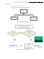
5.2.4
Abnormal display
(Abnormal Image is on Screen (except abnormality in Sustain or Address)
-> Abnormal Display is related with Y-MAIN, X-MAIN, Logic Main, Y-buffer and so on.
This page shows you how to check the boards, and the following pages show you how to find the
defective board.
Abnormal
Dis play
Logic Main
Y – Main
X – Main
[42”SD and 50”HD: LED 2000 blinks
42”HD: LED 2011 blinks
63”HD: LED 2002 blinks]
Figure 5-34 Fault symptom: “Abnormal Display”, general guide line
Y-buffer
G_16380_131.eps
171006
Service Modes, Error Codes, and Fault Finding
SDI PDP 2K6
5.
Y-main
Check
Open
F5001
F5003
Fuse
Replace Y-Board
open?
Shor t
Check
Q5008
Shor t
FET
Replace Y-Board
Q5009
Q5010
Open
Q5013
Short?
X-main
Check
F4000
F4003
Open
Fuse
Replace X-Board
open?
Shor t
Check
Shor t
Q4010
Q4011
FET
Replace X-Board
Q4012
Q4015
Open
Short?
Shor t
Measure
Resistance
Y-buffer
Replace Y-buffer
OUTH
& OUTL
Open
Short?
G_16380_132.eps
190606
Figure 5-35 Fault symptom: “Abnormal Display” 42” SD v5 1/2
[Logic Main]
LED 2000 Blinks
(Motion of Vsync)
Logic main
Normal State
Regular
Abnormal
Replace
board
G_16380_135.eps
190606
Figure 5-36 Fault symptom: “Abnormal Display” 42” SD v5 2/2
EN 45
EN 46
5.
Service Modes, Error Codes, and Fault Finding
SDI PDP 2K6
Y-main
Check
F5001 for Vdd (5V)
F5004 for Vcc (15V)
OPEN
Fuse
Replace Y-Board
F5003 for Vs(200V)
SHORT
Check
SHORT
Q5009 ~ Q5021
FET,IGBT
Replace Y-Board
OPEN
X-main
Check
F4004 for Vdd (5V)
F4001 for Vcc (15V)
OPEN
Fuse
Replace X-Board
F4002 for Vs(200V)
SHORT
Check
FET,IGBT
Q4002,3
SHORT
Replace X-Board
Q4011 ~ Q4016
OPEN
Y-BUFFER
SHORT
Replace Y-BUFFER
OPEN
G_16380_133.eps
190606
Figure 5-37 Fault symptom: “Abnormal Display” 42” HD w1 1/2
[Logic Main]
LED 2011 Blinks
(Motion of Vsync)
Regular
Abnormal
Logic main
Normal State
Replace
board
G_16380_136.eps
190606
Figure 5-38 Fault symptom: “Abnormal Display” 42” HD w1 2/2
Service Modes, Error Codes, and Fault Finding
SDI PDP 2K6
Y-main
Check
F5001
F5000
OPEN
Fuse
Replace Y-B’d
F5003
SHORT
Check
U5009(IPM)
SHORT
FET,IPM
Replace Y-B’d
U5010(IPM)
Q5002~7
OPEN
Q5009
Q5012,13,
Q5027~30
X-main
Check
F4001
F4000
OPEN
Fuse
Replace X-B’d
F4003
SHORT
Check
U4001(IPM)
SHORT
FET,IPM
Replace X-B’d
U4002(IPM)
Q4000 ~ Q4001
OPEN
SHORT
Y-BUFFER
Replace Y-Buffer
Measure
Resistance
OUTH&OUTL
OPEN
Short?
G_16380_134.eps
190606
Figure 5-39 Fault symptom: “Abnormal Display” 50” HD w1 1/2
[Logic Main]
LED 2002 Blinks
(Motion of Vsync)
Regular
Abnormal
Logic main
Normal State
Replace
board
G_16380_137.eps
190606
Figure 5-40 Fault symptom: “Abnormal Display” 50” HD w1 2/2
5.
EN 47
EN 48
5.
SDI PDP 2K6
Service Modes, Error Codes, and Fault Finding
Check
Y-main
F5000
F5001
F5002
F5004
OPEN
Fuse
Check
Replace Y-B’d
SHORT
U5000(IPM)
SHORT
U5001(IPM)
U5002(IPM)
FET,IPM
Replace Y-B’d
Q5002
Q5022~25
OPEN
Q5030~33,
Q5036,38
Q5042~45
X-main
Check
F4000
F4001
F4003
Fuse
OPEN
Replace X-B’d
SHORT
Check
FET,IPM
SHORT
Replace X-B’d
U4003(IPM)
U4005(IPM)
U4006(IPM)
OPEN
Q4002, Q4003
Y-BUFFER
SHORT
Replace Y-Buffer
Measure
Resistance
OUTH&OUTL
OPEN
Short?
G_16380_049.eps
171006
Figure 5-41 Fault symptom: “Abnormal Display” 63” HD v4 1/2
Service Modes, Error Codes, and Fault Finding
SDI PDP 2K6
5.
[Logic Main]
LED 2002 Blinks
(Motion of Vsync)
Regular
Logic main
Abnormal
Normal State
Replace
board
G_16380_050.eps
171006
Figure 5-42 Fault symptom: “Abnormal Display” 63” HD v4 2/2
5.2.5
Horizontal line or block open
(some horizontal lines don’t exist on screen)
Y-FPC
Y-buffer
connector
Poor
Check
Connection Y-buffer
Y-buffer
Reconnection
& Y-FPC
Good
Br oken
Check
Y-buffer connector pin
broken or bent?
Y-buffer
or bent
Replace Y-buffer B’d
connector
Good
Br oken
Check
Y-FPC pin
Y-FPC
or bent
Replace PDP
broken or bent?
G_16380_153.eps
190606
Figure 5-43 Fault symptom: “Horizontal line or block open”
EN 49
EN 50
5.2.6
5.
Service Modes, Error Codes, and Fault Finding
SDI PDP 2K6
Address open
(some vertical lines don’t exist on screen)
-> Address Open is related with Logic Main, Logic Buffer, FFC, TCP and so on.
This page shows you how to check the boards, and the following pages show you how to find
the defective board.
Address Open
Line Open
Data Block Open
TCP Block Open
[ Logic Main/FFC ]
[ Logic Buffer ]
Changing some parts
Changing necessary
Parts (E/F)
G_16380_140.eps
190606
Figure 5-44 Fault symptom: “Address open” 1/2
What is the vertical status of open?
(the open part is black)
1 line or 1 block
uvG
Half block or
Half of screen
open?
Open?
lzG
lzG
Replace
uvG
Replace PDP
Logic-main &
Address Buffer (E/F)
lzG
Done
G_16380_142.eps
190606
Figure 5-45 Fault symptom: “Address open” 2/2
Service Modes, Error Codes, and Fault Finding
5.2.7
SDI PDP 2K6
5.
EN 51
Address short
(some vertical lines appear to be linked on screen)
-> Address Short is related with Logic Main, Logic Buffer, FFC, TCP and so on.
This page shows you how to check the boards, and the following pages show you how to find
the defective board.
Address Short
Line Short
Data Block Short
[ Logic Main/FFC ]
[ Logic Buffer ]
Changing some parts
Changing necessary
Parts (E/F)
G_16380_144.eps
190606
Figure 5-46 Fault symptom: “Address short” 1/2
What is the vertical status of short?
(the shorted part is colored)
1 line or 1 block
NO
Half of screen
short?
short?
YES
YES
NO
Replace PDP
Half block or
Replace
Logic-main &
Address Buffer (E/F)
Figure 5-47 Fault symptom: “Address short” 2/2
YES
Done
G_16380_146.eps
190606
EN 52
5.2.8
5.
Service Modes, Error Codes, and Fault Finding
SDI PDP 2K6
Criteria for Panel Replacement, due to Defective Panel Cells
W
H/8
B- Zone
H
3H/4
A- Zone
H/8
W/2
W/4
W/4
G_16380_508.eps
190606
Figure 5-48 Panel zones 42” SD v5
Specification
Item
Number of cell defects
Non-lighting
Zone A: 0 and less
cell defect
Zone B: 4 and less
Nonextinguishing
cell defect
Zone A: 0
Zone B: 1
Flickering cell
Zone A: 0
defect
Zone B: 1
High Intensity
Zone A: 0
Cell defect
Zone B: 0
Adjacent
Zone A: 0
cell defect
Zone B: 0
Total
cell defects
Distance between cell defects
Regardless of A and B zone
1 Cell Defect in an area of 50 * 50 mm
6 and less
G_16380_509.eps
190606
Figure 5-49 Criteria for panel replacement 42” SD v5
W
H/8
B- Zone
H
3H/4
A- Zone
H/8
W/4
W/2
Figure 5-50 Panel zones 42” HD w1
W/4
G_16380_508.eps
190606
Service Modes, Error Codes, and Fault Finding
Specification
Item
Number of cell defects
Non-lighting
Zone A:
4 and less
cell defect
Zone B:
8 and less
Nonextinguishing
cell defect
Zone B: 1 and less
Zone A: 0
defect
Zone B: 1 and less
Cell defect
Adjacent
cell defect
Total
cell defects
Distance between cell defects
Zone A: 0
Flickering cell
High Intensity
SDI PDP 2K6
Regardless of A and B zone,
Zone A: 0
1 Cell Defect in an area of 50mm*50mm
Zone B: 1 and less
(Only Red & Blue)
Zone A: 0
Zone B: 1 and less
(Only Red & Blue)
12 and less
G_16380_511.eps
190606
Figure 5-51 Criteria for panel replacement 42” HD w1
W
H/4
H
W/4
A- Zone
H/2
B- Zone
H/4
W/2
W/4 G_16380_510.eps
190606
Figure 5-52 Panel zones 50” HD w1
Item
Specification
Number of cell defects
Non-lighting
Zone A:
4 and less
cell defect
Zone B:
8 and less
Nonextinguishing
cell defect
Zone A: 0
Zone B: 1 and less
Flickering cell
Zone A: 0
defect
Zone B: 1 and less
High Intensity
Cell defect
Adjacent
cell defect
Total
cell defects
Distance between cell defects
Regardless of A and B zone,
Zone A: 0
Zone B: 1 and less
1 Cell Defect in an area of 50mm*50mm
(Only Red & Blue)
Zone A: 0
Zone B: 1 and less
(Only Red & Blue)
12 and less
G_16380_511.eps
190606
Figure 5-53 Criteria for panel replacement 50” HD w1
5.
EN 53
EN 54
5.
Service Modes, Error Codes, and Fault Finding
SDI PDP 2K6
H/4
A- Zone
H/2
B- Zone
H/4
W/2
W/4 G_16380_051.eps
H
W/4
171006
Figure 5-54 Panel zones 63” HD v4
Item
Number of cell defects
Non-lighting
Zone A:
2 and less
cell defect
Zone B:
8 and less
Non-
Specification
Distance between cell defects
Zone A: 0
extinguishing
Zone B: 1 and less
cell defect
Flickering cell
Zone A: 0
defect
Zone B: 1 and less
Regardless of A and B zone,
Zone A: 0
High Intensity
Zone B: 1 and less
Cell defect
1 Cell Defect in an area of 50mm*50mm
(No green cell)
Zone A: 0
Adjacent
Zone B: 1 and less
cell defect
(No green cell)
Total
10 and less
cell defects
G_16380_052.eps
171006
Figure 5-55 Criteria for panel replacement 63” HD v4
5.2.9
Overview
Table 5-2 Overview of faults and cures
Condition Name
Description
Related Board
No output voltage
Operating voltages don't exist.
SMPS
No display
Operating voltages exist, but no image on screen
Y-MAIN, X-MAIN, Logic Main, Cables
Abnormal display
Abnormal Image (not open or short) is on screen.
Y-MAIN, X-MAIN, Logic Main
Sustain open
Some horizontal lines are missing on screen
Scan Buffer, FPC of X / Y
Sustain short
Some horizontal lines appear to be linked on screen
Scan Buffer, FPC of X / Y
Address open
Some vertical lines are missing on screen
Logic Main, Logic Buffer, FFC,TCP
Address short
Some vertical lines appear to be linked on screen
Logic Main, Logic Buffer, FFC,TCP
Defective panel cells
Some cells seem to be defective
Check criteria for replacement of the panel
Service Modes, Error Codes, and Fault Finding
5.
EN 55
Defect Description Form
This form must be used by the workshops for warranty claims:
DDF FLAT TV (panels & boards) version 1.1
Date last modified: 08/03/2005
To be filled in by WORKSHOP / WORK CENTER
Philips
Country:
Type nr./Model nr. set
Serial nr. set
LCD & Plasma
Customer Account nr.:
Type nr. display
DEFECT DESCRIPTION
Serial nr. display
FORM
Job sheet nr.:
Part nr display (12nc)
G E N E R A L R E P A IR DA T A
Return number
Condition
Symptom(s)
P A N E L R E P A IR
Pixel
Defect(s):
Symptoms
Out of
warranty
0170 _ _ _ _ _ _
❐
Constantly
❐
In a hot environment
❐
Intermittently
❐
In a cold environment
❐
After a while
❐
Other : …………………………………
❐
No backlight
❐
Flickering / flashing picture
❐
No picture
❐
Lines across/down image
❐
Picture too bright
❐
Inactive row(s)
❐
Shading / smearing on
picture
❐
Inactive column(s)
❐
Missing colour(s)
❐
Other: ………………………………………………
❐
Only partial picture
❐
Unstabel picture
……………………………………………….
Qty of dots :
❐
Dark dots
……..
❐
Bright dots
……..
---------- Picture ----------
Mark
Defect(s)
Insert picture or mark defect !
Following defect symptoms are out of warranty:
• Broken glass
• Number of dark/bright pixels within spec.
• Scratch(es) on display
• Burn in
Spare Part Nr. New Board
B O A R D R E P A IR
5.3
SDI PDP 2K6
(only for Plasma TV)
Barcode Nr. Defect Board
These
symptoms
are not
claimable.
Barcode Nr. Replaced Board
1.
For Plasma
TV repair
only
2.
3.
4.
To be filled in by EUROSERVICE
Note 1:
Note 2:
RMA number:
Date of receipt:
The defective LCD-panel / PDP needs to be returned in the same packaging as the new part was send. If not
the warranty claim will be rejected.
Please fill out this form completely and correctly, otherwise Euroservice is unable to fulfil the repair request!
Owner: PHILIPS CE EUROSERVICE
DE10WEG
F_15590_115.eps
110705
Figure 5-56 Defect Description Form (DDF)
EN 56
6.
SDI PDP 2K6
Block Diagrams, Test Point Overview, and Waveforms
6. Block Diagrams, Test Point Overview, and Waveforms
6.3.2
6.3.3
6.3.4
6.3.5
6.3.6
Index of this chapter:
6.1 Block Diagram for Drive Circuits
6.2 Block Diagram for Logic Circuit
6.3 PSU
6.3.1 PSU Layout, Display Types 42" SD v5, 42" HD w1, and
50" HD w1
6.1
PSU Layout, Display Type 63" HD v4
Voltage Level Overview 42" SD v5
Voltage Level Overview 42" HD w1
Voltage Level Overview 50" HD w1
Voltage Level Overview 63" HD v4
Block Diagram for Drive Circuits
Each
Voltage
from SMPS
Sustain
(Xr, Xf,
Xs, Xg)
X-out
X-bias
(Xe)
Drive signal
from logic
G_16380_218.eps
190606
Figure 6-1 Block diagram X-Main Board
DC-DC
(Vsch, Vccf)
Each
Voltage
from SMPS
Rising ramp
(Yrr)
Y-out
falling ramp
(Yfr)
Sustain
(Yr, Yf,
Ys, Yg)
Scan period
(Ysc)
Drive signal
from logic
G_16380_219.eps
190606
Figure 6-2 Block diagram Y-Main Board
Block Diagrams, Test Point Overview, and Waveforms
6.2
SDI PDP 2K6
Block Diagram for Logic Circuit
Lo g ic M ain Blo ck D iag ram
LVDS
INPUT
( CL OCK
R,G,B Data
V, H Sync.
DE)
I2C
Interfac e
Signal
ASIC
SPS -S101
X, Y
FET
Control
TCP
CLK, DATA
Control
128 M
128K
DDR
128M
128K
DDR
G_16380_222.eps
190606
Figure 6-3 Block diagram (42" SD v5)
Logic Main Block Diagram
LVDS
Input
(Clock
RGB data
V-H-sync.
DE)
ASIC
SPS-H102
X-Y
FET
Control
TCP
CLK, DATA
UART
Interface
Signal
Control
128M
DDR
128M
DDR
G_16380_223.eps
190606
Figure 6-4 Block diagram (42" HD w1)
Logic Main Block Diagram
LVDS
Input
(Clock
RGB data
V-H-sync.
DE)
ASIC
SPS-H102
X-Y
FET
Control
TCP
CLK, DATA
I2C
Interface
Signal
Control
128M
DDR
128M
DDR
Figure 6-5 Block diagram (50" HD w1 and 63” HD v4)
G_16380_224.eps
190606
6.
EN 57
EN 58
6.
SDI PDP 2K6
Block Diagrams, Test Point Overview, and Waveforms
6.3
PSU
6.3.1
PSU Layout, Display Types 42" SD v5, 42" HD w1, and 50" HD w1
G_16380_225.eps
120606
Figure 6-6 PSU layout (42" SD v5, 42" HD w1, and 50" HD w1)
Block Diagrams, Test Point Overview, and Waveforms
6.3.2
SDI PDP 2K6
6.
EN 59
PSU Layout, Display Type 63" HD v4
Package 1, Main Supply
G_16380_053.eps
201006
Figure 6-7 PSU layout (63" HD v4, Main PSU)
EN 60
6.
SDI PDP 2K6
Block Diagrams, Test Point Overview, and Waveforms
G_16380_054.eps
201006
Package 2, Sub Supply
Figure 6-8 PSU layout (63" HD v4, Sub PSU))
Block Diagrams, Test Point Overview, and Waveforms
6.3.3
SDI PDP 2K6
Voltage Level Overview 42" SD v5
Table 6-1 Voltage level overview (also refer to the sticker on the rear side of the panel)
No
Output voltage (V)
Voltage Setting (Normal Load)
Output Voltage Range
1
VS
207 V ± 1 %
195 V ~ 215 V
2
VA
65 V ± 1.5 %
50 V ~ 70 V
3
VE
110 V ± 1.5 %
70 V ~ 110 V
4
VSET
201 V ± 1.5 %
180 V ~ 210 V
5
VSCAN
-190 V ± 1.5 %
-190 V ~ -170 V
6
VSB
5V±5%
Fixed
7
VG
15 V ± 5 %
Fixed
8
D5VL
5.2 V ± 5 %
Fixed
9
D3V3
3.3 V ± 5 %
Fixed
Check voltage label on the PDP for correct values.
6.3.4
Voltage Level Overview 42" HD w1
Table 6-2 Voltage level overview (also refer to the sticker on the rear side of the panel)
No
Output voltage (V)
Voltage Setting (Normal Load)
Output Voltage Range
1
VS
200 V ± 1.5 %
198 V ~ 202 V
2
VA
65 V ± 1.5 %
63 V ~ 67 V
3
VE
110 V ± 1.5 %
105 V ~ 115 V
4
VSET
195 V ± 1.5 %
193 V ~ 197 V
5
VSCAN
-190 V ± 1.5 %
-192 V ~ -188 V
6
VG
15 V ± 5 %
Fixed
7
D5VL
5.2 V ± 5 %
Fixed
8
D3V3
3.3 V ± 5 %
Fixed
Check voltage label on the PDP for correct values.
6.3.5
Voltage Level Overview 50" HD w1
Table 6-3 Voltage level overview (also refer to the sticker on the rear side of the panel)
No
Output voltage (V)
Voltage Setting (Normal Load)
Output Voltage Range
1
VS
202 V ± 1 %
190 V ~ 210 V
2
VA
65 V ± 1.5 %
55 V ~ 75 V
3
VE
115 V ± 1.5 %
110 V ~ 130 V
4
VSET
190 V ± 1.5 %
170 V ~ 200 V
5
VSCAN
-190 V ± 1.5 %
-210 V ~ -180 V
6
VSB
5V±5%
Fixed
7
VG
15 V ± 5 %
Fixed
8
D5VL
5.2 V ± 5 %
Fixed
9
D3V3
3.3 V ± 5 %
Fixed
Check voltage label on the PDP for correct values.
6.3.6
Voltage Level Overview 63" HD v4
Table 6-4 Voltage level overview (also refer to the sticker on the rear side of the panel)
No
Output voltage (V)
Voltage Setting (Normal Load)
Output Voltage Range
1
VS
184 V ± 1 %
165 V ~ 190 V
2
VA
72 V ± 1.5 %
60 V ~ 85 V
3
VE
88 V ± 1.5 %
80 V ~ 110 V
4
VSET
178 V ± 1.5 %
160 V ~ 200 V
5
VSCAN
-160 V ± 1.5 %
-190 V ~ -155 V
6
VSB
5V±5%
Fixed
7
VG
15 V ± 5 %
Fixed
8
D5VL
5.3 V ± 5 %
Fixed
9
D3V3
3.4 V ± 5 %
Fixed
Check voltage label on the PDP for correct values.
6.
EN 61
EN 62
7.
SDI PDP 2K6
Circuit Diagrams and PWB Layouts
7. Circuit Diagrams and PWB Layouts
Not applicable.
8. Alignments
Index of this chapter:
8.1 Power Supply Voltages
8.2 Waveform Alignments 42” SD v5
8.3 Waveform Alignments 42” HD w1
8.4 Waveform Alignments 50” HD w1
8.5 Waveform Alignments 63” HD v4
Note:
• Figures can deviate due to the different model executions.
Important: Remove all non-default jumpers and reset all DIP
switches, after the repair!
8.1
Power Supply Voltages
8.1.1
Location of potentiometers and test points on the PSU of
42”SD v5, 42” HD w1, and 50” HD w1
G_16380_225.eps
120606
Figure 8-1 Location of potentiometers and test points on the PSU of 42”SD v5, 42” HD w1, and 50” HD w1
Alignments
8.1.2
SDI PDP 2K6
8.
EN 63
Location of potentiometers and test points on the PSU of
63” HD v4
Ve
Vs
Va
Vset
5V
Vscan
3.4V
G_16380_058.eps
171006
Figure 8-2 Location of potentiometers on the PSU of 63” HD v4
Va
RTN
Vs
Vscan
Vset
Ve
RTN
G_16380_059.eps
171006
Figure 8-3 Location of test points on the PSU of 63” HD v4
EN 64
8.1.3
8.
SDI PDP 2K6
Alignments
Adjustment Power Supply Voltages 42" SD v5
Table 8-1 Adjustment voltage level overview (also refer to the sticker on the rear side of the panel)
No
Output voltage (V)
Voltage Setting (Normal Load)
Output Voltage Range
1
VS
207 V ± 1 %
195 V ~ 215 V
2
VA
65 V ± 1.5 %
50 V ~ 70 V
3
VE
110 V ± 1.5 %
70 V ~ 110 V
4
VSET
201 V ± 1.5 %
180 V ~ 210 V
5
VSCAN
-190 V ± 1.5 %
-190 V ~ -170 V
6
VSB
5V±5%
Fixed
7
VG
15 V ± 5 %
Fixed
8
D5VL
5.2 V ± 5 %
Fixed
9
D3V3
3.3 V ± 5 %
Fixed
Check voltage label on the PDP for correct values.
Vs
Vs
Ve
Vset
Vcc
Vscan
Vcc
D5V
D5V
Va
D3V3
G_16380_501.eps
190606
Figure 8-4 Location of the supply lines from the PSU to the boards - 42” SD v5
Alignments
SDI PDP 2K6
Y-main
8.
X-main
Vs [F500 3]
Vset [R 5035]
Vs [F4002]
Ve [L4017]
Vscan [R5015]
Vcc [F5001]
Vcc [F4000]
G_16380_502.eps
190606
Figure 8-5 Location of the test points for the supply voltages - 42” SD v5
8.1.4
Adjustment Power Supply Voltages 42" HD w1
Table 8-2 Adjustment voltage level overview (also refer to the sticker on the rear side of the panel)
No
Output voltage (V)
Voltage Setting (Normal Load)
Output Voltage Range
1
VS
200 V ± 1.5 %
198 V ~ 202 V
2
VA
65 V ± 1.5 %
63 V ~ 67 V
3
VE
110 V ± 1.5 %
105 V ~ 115 V
4
VSET
195 V ± 1.5 %
193 V ~ 197 V
5
VSCAN
-190 V ± 1.5 %
-192 V ~ -188 V
6
VG
15 V ± 5 %
Fixed
7
D5VL
5.2 V ± 5 %
Fixed
8
D3V3
3.3 V ± 5 %
Fixed
Check voltage label on the PDP for correct values.
EN 65
EN 66
8.
Alignments
SDI PDP 2K6
Vs
Vset
Vs
Vscan
Ve
Vcc
Vcc
D5V
D3V3
D5V
Va
G_16380_503.eps
160606
Figure 8-6 Location of the supply lines from the PSU to the boards - 42” HD w1
Alignments
SDI PDP 2K6
8.
EN 67
Drive board’s voltage check point
Y- main Voltage Check Point
YM
YM
YM
Vs (200V) – F5003
YM
Vsch (-70V) – Vsch TP
YM
5.5V (5.5V) – F5001
Vscan (-190V) – R5081
Vset (195V) – R5048
YM Vccf (Vscan + 15V) – Vccf TP
YM
Vcc (15V) – F5004
Figure 8-7 Location of the test points for the supply voltages - Y-main - 42” HD w1
G_16380_504.eps
160606
EN 68
8.
SDI PDP 2K6
Alignments
TG}GjGwG
Vs (200V) – F4003
Ve (110V) – F4005
Vcc (15V) – F4001
5.5V (5.5V) – F4004
Figure 8-8 Location of the test points for the supply voltages - X-main - 42” HD w1
8.1.5
Adjustment Power Supply Voltages 50" HD w1
Table 8-3 Adjustment voltage level overview (also refer to the sticker on the rear side of the panel)
No
Output voltage (V)
Voltage Setting (Normal Load)
Output Voltage Range
1
VS
202 V ± 1 %
190 V ~ 210 V
2
VA
65 V ± 1.5 %
55 V ~ 75 V
3
VE
115 V ± 1.5 %
110 V ~ 130 V
4
VSET
190 V ± 1.5 %
170 V ~ 200 V
5
VSCAN
-190 V ± 1.5 %
-210 V ~ -180 V
6
VSB
5V±5%
Fixed
7
VG
15 V ± 5 %
Fixed
8
D5VL
5.2 V ± 5 %
Fixed
9
D3V3
3.3 V ± 5 %
Fixed
Check voltage label on the PDP for correct values.
G_16380_505.eps
160606
Alignments
SDI PDP 2K6
8.
Vs
Vset
Vs
Vscan
Ve
Vcc
Vcc
D5V
Va
D5V
D3V3
G_16380_506.eps
160606
Figure 8-9 Location of the supply lines from the PSU to the boards - 50” HD w1
Y-main
X-main
Vset [TP]
Vs [F5003]
Vs [F400 3]
Vcc [F5000]
Vscan [TP]
Vdd [F5001]
Vcc [F4 000]
Ve [TP]
Vdd [F4001]
G_16380_507.eps
160606
Figure 8-10 Location of the test points for the supply voltages - 50” HD w1
EN 69
EN 70
8.1.6
8.
Alignments
SDI PDP 2K6
Adjustment Power Supply Voltages 63" HD v4
Table 8-4 Adjustment voltage level overview (also refer to the sticker on the rear side of the panel)
No
Output voltage (V)
Voltage Setting (Normal Load)
Output Voltage Range
1
Vs
184 V ± 1 %
165 V ~ 190 V
2
Va
72 V ± 1.5 %
60 V ~ 85 V
3
Ve
88 V ± 1.5 %
80 V ~ 110 V
4
Vset
178 V ± 1.5 %
160 V ~ 200 V
5
Vscan
-160 V ± 1.5 %
-190 V ~ -155 V
6
Vsb
5V±5%
Fixed
7
Vg
15 V ± 5 %
Fixed
8
D5VL
5.3 V ± 5 %
Fixed
9
D3V3
3.4 V ± 5 %
Fixed
Check voltage label on the PDP for correct values.
Vs
Vset
Vscan
Vcc
Vs
Ve
Vcc
D5V
Va
D5V
D3V3
G_16380_055.eps
171006
Figure 8-11 Location of the supply lines from the PSU to the boards - 63" HD v4
Alignments
Y-main
SDI PDP 2K6
8.
EN 71
X-main
Vs [F5002]
Vs [F4003]
Vset [TP]
Vcc [F5000]
Ve [TP]
Vdd [F5001]
Vcc [F4000]
Vsch [TP]
Vdd [F4001]
G_16380_057.eps
171006
Figure 8-12 Location of the test points for the supply voltages - 63" HD v4
8.2
Waveform Alignments 42” SD v5
1. Set the pattern to Full White (put a jumper on pins 1 and 2
of CN2012 of the Logic Board).
2. Check the waveform using an Oscilloscope.
• Triggering through V_TOGG of the LOGIC Board (see
Figure “Logic PWB”).
• Connect the “OUT240” test point, located at the centre
of the Y-buffer PWB, to the other channel, and then
check the first Subfield waveform of one TV-Field.
• Check the waveform by adjusting the Horizontal
Division of the oscilloscope.
3. Adjust the waveform of the rising ramp with VR5000 (see
Figure “Rising ramp waveform adjustment”).
4. Adjust the waveform of the falling ramp with VR5001 (see
Figure “Falling ramp waveform adjustment”).
EN 72
8.
SDI PDP 2K6
Alignments
G_16380_401.eps
160606
Figure 8-13 Waveform adjustment (Y-Board) - 42 SD v5
mGG
XWW}
zGG
<Rising r amp>
The second point is located 100 V
YWWG
below and 200 sec before the first
point.
G_16380_402.eps
160606
Figure 8-14 Rising ramp waveform (Y-Board) - 42 SD v5
<Falling r amp>
The second point is located 50 Volt
above and 160 usec before the first
point.
X]WG
zGG
\W}G
mGG
G_16380_403.eps
160606
Figure 8-15 Falling ramp flat time adjustment (Y-Board) - 42 SD v5
Alignments
SDI PDP 2K6
8.
EN 73
V R 5 0 0 0 a d ju s t m e n t
R is in g ra m p
V R 5 0 0 1 a d ju s t m e n t
F a lli n g r a m p
G_16380_404.eps
160606
Figure 8-16 Potentiometer locations - 42 SD v5
Jumpers
Test points
Figure 8-17 Logic PWB - 42 SD v5
G_16380_409.eps
160606
EN 74
8.3
8.
Alignments
SDI PDP 2K6
Waveform Alignments 42” HD w1
•
1. Set the pattern to Full White:
• Place jumpers on:
– J8902 of the PSU alarm board
– J5003 and J5004 of the PSU
– Pins 1 and 2 of CN2072 on the Logic Board
• When the display starts showing a cycle of different
patterns, push button SW2001 for at least one second.
Now the display shows a continuous full white pattern.
To restart the cycle of different patterns, push the
button once more and wait for a few seconds.
2. Check the waveform using an Oscilloscope.
• Triggering through V_TOGG of the LOGIC Board (see
Figure “Logic PWB”).
Connect the “OUT240” test point, located at the centre
of the Y-buffer PWB, to the other channel, and then
check the first Subfield waveform of one TV-Field.
• Check the waveform by adjusting the Horizontal
Division of the oscilloscope.
• Check the waveform by adjusting the Horizontal
Division of the oscilloscope.
• Check the Reset waveform when the V_TOGG level is
changed.
3. Adjust the waveform of the rising ramp with VR5001 (see
Figure “Rising ramp waveform adjustment”).
4. Adjust the waveform of the falling ramp with VR5002 (see
Figure “Falling ramp waveform adjustment”).
VR5001 Adjustment : Rising Ramp
Oscilloscope Setting : 50V / 40us
VR5002 Adjustment : Falling Ramp
Oscilloscope Setting : 50V / 40us
G_16380_405.eps
160606
Figure 8-18 Adjusting procedure - 42” HD w1
Jumper
Push button
Vtogg
Figure 8-19 Logic PWB - 42 HD w1
G_16380_410.eps
160606
Alignments
8.4
Waveform Alignments 50” HD w1
SDI PDP 2K6
8.
EN 75
•
Check the waveform by adjusting the Horizontal
Division of the oscilloscope.
• Check the waveform by adjusting the Horizontal
Division of the oscilloscope.
• Check the Reset waveform when the V_TOGG level is
changed.
3. Adjust the waveform of the rising ramp with VR5001 (see
Figure “Rising ramp waveform adjustment”).
4. Adjust the waveform of the falling ramp with VR5002 (see
Figure “Falling ramp waveform adjustment”).
1. Set the pattern to Full White:
• Place jumpers on:
– J8902 of the PSU alarm board
– J5003 and J5004 of the PSU
– Pin 1 and 2 of CN2072 on the Logic Board
• When the display starts showing a cycle of different
patterns, push button SW2001 for at least one second.
Now the display shows a continuous full white pattern.
To restart the cycle of different patterns, push the
button once more and wait for a few seconds.
2. Check the waveform using an Oscilloscope.
• Triggering through V_TOGG of the LOGIC Board (see
Figure “Logic PWB”).
• Connect the “OUT240” test point, located at the centre
of the Y-buffer PWB, to the other channel, and then
check the first Subfield waveform of one TV-Field.
Special notice: It is very important, that you execute this
adjustment on the 1st Sub-Field (SF) of the 1st Frame of the
Reset waveform and then move to the 3rd Sub-field for
adjusting.
Rising ramp
Falling ramp
< Main Reset Waveform>
Adjust VR5000 to set the time of Yrr
Adjust VR5001 to set the time of Yfr
(Main Reset Rising Ramp) like the
(Main Reset Falling Ramp) like the
below picture.
Oscilloscope Setting : 50V / 20us
below picture.
Oscilloscope Setting : 50V / 20us
Point of intersection
1 block
8 blocks
6 blocks
1 block
Point of intersection
<Rising Ramp>
<Falling Ramp>
Figure 8-20 TCP ramp waveform inclination adjustment (Y-Board)
G_16380_406.eps
160606
EN 76
8.
SDI PDP 2K6
Alignments
VR5000 Adjustment :
Adjust VR5000 to set the time of Yrr
(Main Reset Rising Ramp) like the
picture of front page.
Oscilloscope Setting : 50V / 20us
VR5001 Adjustment :
Adjust VR5001 to set the time of Yfr
(Main Reset Falling Ramp) like the
picture of front page.
Oscilloscope Setting : 50V / 20us
G_16380_407.eps
160606
Figure 8-21 Potentiometer locations (Y-Board) - 50 HD w1
Vtogg
Jumper
G_16830_408.eps
160606
Figure 8-22 Logic Main board - 50 HD w1
Alignments
8.5
Waveform Alignments 63” HD v4
SDI PDP 2K6
8.
EN 77
check the first Subfield operating waveform of one TVField.
• Check the waveform by adjusting the Horizontal
Division of the oscilloscope.
• Check the Reset waveform when the V_TOGG level is
changed.
3. Adjust the intersection point of the rising ramp with VR5000
(see Figure “Rising ramp waveform adjustment”).
4. Adjust the intersection point of the falling ramp with
VR5001 (see Figure “Falling ramp waveform adjustment”).
1. Set the pattern to Full White:
• Place a jumper on CN2012 on the Logic Board and
switch the display “ON”.
2. Check the waveform using an Oscilloscope.
• Triggering through V_TOGG of the LOGIC Board (see
Figure “Logic PWB”).
• Connect the “OUT240” test point, located at the centre
of the Y-buffer PWB, to the other channel, and then
W1 Ramp Waveform Inclination Adjustment ( Y-Board )
yGy
wG
< Main Reset Waveform>
Adjust VR5000 to set the time of Yrr
Adjust VR5001 to set the time of Yfr
(Main Reset Rising Ramp) like the
(Preset) like the below picture.
Oscilloscope Setting : 20V / 40us
below picture.
Oscilloscope Setting : 20V / 40us
XGi
wGGG
]GiG
\GiG
G G G G G G G GwGG
<Rising Ramp>
<Preset>
Figure 8-23 TCP ramp waveform inclination adjustment (Y-Board)
XGi
G_16380_061.eps
181006
EN 78
8.
SDI PDP 2K6
Alignments
VR5000 Adjustment :
Adjust VR5000 to set the time of Yrr
(Main Reset Rising Ramp) like the
picture of the previous page.
Oscilloscope Setting : 20V / 40us
VR5001 Adjustment :
Adjust VR5001 to set the time of Yfr
(Preset) like the picture of the previous page.
Oscilloscope Setting : 20V /40us
G_16380_062.eps
181006
Figure 8-24 Potentiometer locations (Y-Board) - 50 HD w1
Vtogg
Jumper
Figure 8-25 Logic Main board - 63” HD v4
G_16830_060.eps
181006
Circuit Descriptions, Abbreviation List, and IC Data Sheets
SDI PDP 2K6
9.
EN 79
9. Circuit Descriptions, Abbreviation List, and IC Data Sheets
Index of this chapter:
9.1 Main function of Each Assembly
9.2 Abbreviation List
9.3 IC Data Sheets
9.1
Main function of Each Assembly
9.1.1
X Main Board
9.2
AC
COF
DC
ERC
ESD
FET
FFC
FPC
FTV
HD
I/O
IC
LB
LED
LVDS
PCB
PDP
PSU
PWB
RGB
SD
SDI
SMPS
SSB
SF
TCP
VR
Vsc
YBL
YBU
YM
The X Main board generates a drive signal by switching the
FET in synchronization with logic main board timing, and
supplies the X electrode of the panel with the drive signal
through the connector.
1. Maintain voltage waveforms (including ERC).
2. Generate X rising ramp signal.
3. Maintain Ve bias between Scan intervals.
9.1.2
Y Main Board
The Y Main board generates a drive signal by switching the
FET in synchronization with the logic Main Board timing and
sequential supplies the Y electrode of the panel with the drive
signal through the scan driver IC on the Y-buffer board. This
board connected to the panel’s Y terminal has the following
main functions.
1. Maintain voltage waveforms (including ERC).
2. Generate Y-rising Falling Ramp.
3. Maintain V scan bias.
9.1.3
Logic Main Board
The Logic Main board generates and outputs the address drive
output signal and the X,Y drive signal by processing the video
signals. This Board buffers the address drive output signal and
feeds it to the address drive IC (COF module, video signal- X Y
drive signal generation, frame memory circuit / address data
rearrangement).
9.1.4
Logic Buffer (E, F)
The Logic Buffer transmits data signal and control signal.
9.1.5
Y Buffer Board (Upper, Lower)
The Y Buffer board consisting of the upper and lower boards
supplies the Y-terminal with scan waveforms. The board
comprises eight scan driver ICs (ST microelectronics STV
7617: 64 or 65 output pins), but four ICs for the SD class.
9.1.6
AC Noise Filter
The AC Noise filter has function for removing noise (low
frequency) and blocking surge. It affects safety standards
(EMC, EMI).
9.1.7
TCP (Tape Carrier Package)
The TCP applies the Va pulse to the address electrode and
constitutes address discharge by the potential difference
between the Va pulse and the pulse applied to the Y electrode.
The TCP comprise four data driver ICs (STV7610A: 96 pins
output pins). Seven TCPs are required for signal scan.
Abbreviation List
9.3
IC Data Sheets
Not applicable.
Alternating Current
Circuit On Foil
Direct Current
Energy Recovery Circuit
Electro Static Discharge
Field Effect Transistor
Flat Foil Cable
Flexible Printed Circuit
Flat TeleVision
High Definition
Input/Output
Integrated Circuit
Logic Buffer
Light Emitting Diode
Low Voltage Differential Signalling
Printed Circuit Board (same as PWB)
Plasma Display Panel
Power Supply Unit
Printed Wiring Board (same as PCB)
Red, Green, Blue colour space
Standard Definition
Samsung Display Industry (supplier)
Switched Mode Power Supply
Small Signal Board
Sub Field
Tape Carrier Package
Variable Resistor
Scan Voltage
Y Buffer Lower board
Y Buffer Upper board
Y Main board
EN 80
10.
Spare Parts List
SDI PDP 2K6
10. Spare Parts List
•
Notes;
• Determine the SDI part / model number of the PDP.
• Find the SDI part number on the actual board to be
replaced.
SDI part numbers begin with “LJ92”, except for the SMPS
the part number begins with “LJ44”.
• Find the SDI board part number in the spare parts
overview.
• Find the SDI part number in this overview that matches the
part number that is actually on the original board.
• Cross the SDI board part number to the Philips part
number.
• Order the Philips part number.
Note: The appearance of a leaded and lead-free board can
be different; the colour of the PWB and also the layout of
the components are sometimes different.
E_06532_026.eps
081105
Figure 10-1 Lead-free logo SDI
Table 10-1 Spare parts overview
PDP type
PDP 12 NC
42 SD v5
42 HD w1
50 HD w1
63 HD v4
9322 233 14682
9322 240 08682
9322 240 25682
9322 246 18682
PDP model type and version
S42SD-YD09
PP42SD-019A
S42AX-YD02
BOARDS
Logic-Buffer (E)
SDI part #
12NC
LJ92-01322B
9965 000 37577
Logic-Buffer (F)
LJ92-01323B
Logic-Buffer (G)
-
Y-Buffer
Y-Buffer (up)
Y-Buffer (down)
PP42AX-009A
S50HW-YD01
PP50HW-010A
S63HW-YD05
PP63HW-005A
SDI part #
12NC
LJ92-01343A
9965 000 36813
SDI part #
12NC
SDI part #
12NC
LJ92-01372A
9965 000 36826
LJ92-01193A
9965 000 42586
9965 000 37608
LJ92-01342A
9965 000 36814
LJ92-01373A
9965 000 36827
LJ92-01194A
9965 000 42587
-
-
-
LJ92-01374A
9965 000 36828-
LJ92-01195A
9965 000 42588-
LJ92-01339A
9965 000 36812
LJ92-01344A
9965 000 36819
-
-
-
-
-
-
-
-
LJ92-01276C
9965 000 36824
LJ92-01437A
9965 000 42589
-
-
-
-
LJ92-01277C
9965 000 36825
LJ92-01438A
9965 000 42590
Logic-Board
LJ92-01287C
9965 000 37576
LJ92-01370B
9965 000 36815
LJ92-01371B
9965 000 36820
LJ92-01289C
9965 000 36820
X-Main Board
LJ92-01340A
9965 000 36810
LJ92-01345A
9965 000 36817
LJ92-01388A
9965 000 36822
LJ92-01385A
9965 000 42594
Y-Main Board
LJ92-01341A
9965 000 36811
LJ92-01346A
9965 000 36818
LJ92-01391A
9965 000 36823
LJ92-01386A
9965 000 42595
SMPS (PSU)
LJ44-00101C
9965 000 33880
LJ44-00117A
9965 000 36816
LJ44-00118A
9965 000 36821
LJ44-00123A
9965 000 42596
SMPS (Sub PSU)
-
-
-
-
-
-
LJ44-00124A
9965 000 42597
X-Buffer (up)
-
-
-
-
-
-
LJ92-01375A
9965 000 42591
X-Buffer (down)
-
-
-
-
-
-
LJ92-01376A
9965 000 42592
CABLES + CONNECTORS
SDI part #
12NC
SDI part #
12NC
SDI part #
12NC
SDI part #
12NC
Cable-flat Logic + Y-Main
LJ39-00164A
9965 000 37609
LJ39-00265A
9965 000 37612
3809-001789
9965 000 37614
3809-001546
996500042799
Cable-flat Logic + X-Main
LJ39-00252A
9965 000 37610
LJ39-00264A
9965 000 37613
3809-001788
9965 000 37615
3809-001695
996500042800
Cable-flat Logic + Logic Buf (E)
3809-001791
9965 000 37611
3809-001629
9965 000 37617
3809-001771
9965 000 37618
-
-
Cable-flat Logic + Logic Buf (F)
3809-001791
9965 000 37611
3809-001629
9965 000 37617
3809-001771
9965 000 37618
-
-
Cable-flat Logic + Logic Buf (G)
-
-
-
-
3809-001790
9965 000 37616
-
-
Cable-flat Logic + Logic Buf (E) upper
-
-
-
-
-
-
3809-001743
996500042801
Cable-flat Logic + Logic Buf (F) upper
-
-
-
-
-
-
3809-001742
996500042802
Cable-flat Logic + Logic Buf (G) upper
-
-
-
-
-
-
3809-001745
996500042803
Cable-flat Logic + Logic Buf (E) lower
-
-
-
-
-
-
3809-001744
996500042804
Cable-flat Logic + Logic Buf (F) lower
-
-
-
-
-
-
3809-001741
996500042805
Cable-flat Logic + Logic Buf (G) lower
-
-
-
-
-
-
3809-001768
996500042806
Connector Logic Buf (E)+Logic Buf (F)
LJ39-00202A
9965 000 37619
LJ39-00259A
9965 000 37623
LJ39-00257A
9965 000 37627
LJ39-00215A
996500042807
Connector Logic Buf (F)+Logic Buf (G)
-
-
-
-
LJ39-00257A
9965 000 37627
LJ39-00215A
996500042807
LJ39-00256A
9965 000 37620
LJ39-00241A
9965 000 37624
LJ39-00266A
9965 000 37628
-
-
-
-
-
-
-
-
LJ39-00234A
996500042808
Connector SMPS + Logic Buf (E)
Connector SMPS + Logic Buf (E) upper
Connector SMPS + Logic Buf (E) lower
-
-
-
-
-
-
LJ39-00184A
996500042809
Connector SMPS + Logic Main
LJ39-00209A
9965 000 37621
LJ39-00155A
9965 000 37625
LJ39-00266A
9965 000 37628
LJ39-00293A
996500042810
Connector SMPS + Y-Main
LJ39-00263A
9965 000 37626
LJ39-00263A
9965 000 37626
LJ39-00221A
9965 000 37629
LJ39-00239A
996500042811
Connector SMPS + X-Main
LJ39-00262A
9965 000 37622
LJ39-00262A
9965 000 37622
LJ39-00220A
9965 000 37630
LJ39-00185A
996500042812
CTN / Chassis
Sets/Chassis in which this PDP type is
used (this list is for indicative purposes
only, we do not pretend it is complete)
CTN
Chassis
CTN
Chassis
CTN
Chassis
CTN
Chassis
42PF5521D/10
LC4.41E AB
42PF9431D/37
BJ2.5U PA
50PF9631D/37
BJ2.4U PA
63PF9631D/37
BJ3.0U PA
42PF5521D/12
LC4.41E AB
42PF9631D/37
BJ2.4U PA
50PF9731D/37
BJ2.4U PA
-
-
Revision List
11. Revision List
Manual xxxx xxx xxxx.0
• First release.
Manual xxxx xxx xxxx.1
• Name changed from “SDI PDP Repair Manual” to “SDI
PDP 2K6”.
• Model 63” HD v4 added.
SDI PDP 2K6
11.
EN 81