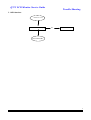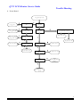
1
Q7C3 LCD Monitor Service Guide
Engineering Specification
Table of Contents
1. Introduction ...................................................................................................................................4
2. Operational Specification ..........................................................................................................4
2.1 Environment.................................................................................................................................4
2.1.1 Temperature ..................................................................................................................................................... 4
2.1.2 Relative Humidity ........................................................................................................................................... 4
2.1.3 Altitude ............................................................................................................................................................. 4
2.2 Transportation .............................................................................................................................5
2.2.1 Vibration Test (Package, Non-Operating)................................................................................................... 5
2.2.2 Drop Test (Package, Non-Operating) .......................................................................................................... 5
2.2.3 Vibration Test (Unpackaged, Non-Operating) ........................................................................................... 6
2.2.4 HALF-SINE SHOCK ..................................................................................................................................... 6
2.3 Packing Configuration ................................................................................................................6
2.3.1 Container Specification .................................................................................................................................. 6
2.3.2 Carton Specification ....................................................................................................................................... 7
2.3.3 Pallet Specification ......................................................................................................................................... 8
2.3.4 Container Carrying Capacity ......................................................................................................................... 8
2.4 Electrostatic Discharge Requirements.......................................................................................8
2.5 Safety Requirements....................................................................................................................8
2.6 EMI Requirements ......................................................................................................................8
2.7 Reliability......................................................................................................................................9
2.8 Mechanical Design for TCO 03: .................................................................................................9
2.9 Environment Protection Design: ................................................................................................9
2.10 Acoustical Noise .........................................................................................................................9
3. Input / Output Signal Specification .......................................................................................9
3.1 Input Signal Requirements .........................................................................................................9
3.1.1 Signal cable (Directly attached to unit) ....................................................................................................... 9
3.1.2 Video signals: .................................................................................................................................................. 10
3.1.3 Sync signal:...................................................................................................................................................... 10
3.2 Function ........................................................................................................................................11
3.2.1 Support timing ................................................................................................................................................. 11
3.3 Number of display colors: ...........................................................................................................12
3.4 Adjustment function ....................................................................................................................12
3.5 Power Supply Requirements.......................................................................................................12
3.5.1 Input Power Requirements ............................................................................................................................ 12
3.5.2 Output Power Requirement ........................................................................................................................... 13
1
Q7C3 LCD Monitor Service Guide
Engineering Specification
Table of Contents
3.5.3 Power Management ........................................................................................................................................ 13
3.6
Specification of Inverter ...........................................................................................................13
3.7 Panel optical Characteristics ......................................................................................................14
4. Functional specification .............................................................................................................16
4.1 Display Quality.............................................................................................................................16
4.1.1 Display Data Area (with full white pattern) ................................................................................................ 16
4.1.2 Video Performance ......................................................................................................................................... 16
4.1.3 Light Output .................................................................................................................................................... 16
4.1.4 Brightness Adjustment Range ....................................................................................................................... 16
4.2 Audio Quality ...............................................................................................................................16
4.2.1 Preamp + Poweramp: ..................................................................................................................................... 16
4.2.2 Speaker Driver: ............................................................................................................................................... 16
4.2.3 Audio Controls: ............................................................................................................................................... 16
5. Physical Specifications................................................................................................................17
5.1 Physical Dimension & Appearance ............................................................................................17
5.1.1 Overall Dimensions: ....................................................................................................................................... 17
5.1.2 Outer Appearance: .......................................................................................................................................... 17
5.2 Construction and Materials on outer surface ...........................................................................17
5.3 Base ...............................................................................................................................................17
5.4 Marking & Labels........................................................................................................................17
5.4.1 Reference Label (Rear panel)........................................................................................................................ 17
5.4.2 Controls & Connectors................................................................................................................................... 17
5.5 Packaging......................................................................................................................................17
5.5.1 Carton Dimension: .......................................................................................................................................... 17
5.5.2 Shipping Weight: ............................................................................................................................................ 17
5.5.3 Shipping Container: ........................................................................................................................................ 17
6. Maintainability Specifications .................................................................................................17
6.1 General & Requirements ............................................................................................................17
6.1.1 Installation: ...................................................................................................................................................... 17
6.1.2 Periodic Maintenance: .................................................................................................................................... 17
6.1.3 Repair & Calibration: ..................................................................................................................................... 17
6.2 Mean Time to Repair...................................................................................................................17
6.2.1 Module Level: ................................................................................................................................................. 17
6.2.2 Component Level: .......................................................................................................................................... 17
6.3 Accessibility ..................................................................................................................................18
6.3.1 General: ............................................................................................................................................................ 18
2
Q7C3 LCD Monitor Service Guide
Engineering Specification
Table of Contents
6.3.2 Outside Cabinet, access to the following elements .................................................................................... 18
6.3.3 Cover Removal, Access ................................................................................................................................. 18
6.4 Equipment & Tools Required.....................................................................................................18
6.4.1 Standard Test Equipment ............................................................................................................................... 18
6.4.2 Documentation ................................................................................................................................................ 18
6.5 Electrical Emission and Energy Saving summary for TCO 03 ...............................................18
6.5.1 Electrical Field(AC): ...................................................................................................................................... 18
6.5.2 Magnetic Field(AC): ...................................................................................................................................... 18
6.5.3 Energy Saving: ................................................................................................................................................ 18
Appendix 1 – Shipment Conditions..................................................................................................18
Fig. 1
Physical Dimension Front View and Side view .................................................................19
3
Q7C3 LCD Monitor Service Guide
Engineering Specification
1. Introduction
This specification describes a 17.0” color TFT LCD monitor which is supported by analog interface solution and support
maximum resolution 1280x1024 at 76 Hz refresh rate. It has the following features:
- User controls:
(a) “Power on/off” switch.
(b) “Exit” key( Back to main menus or leave OSD menu and hot key of Volume adjustment).
(c) “I-key”( For auto adjust vertical position, phase, horizontal position and pixel clock ).
(d) “Enter” key(For enter sub-menus or select items.).
(e) “Left” key (Select left, decreasing adjust and hot key of Contrast adjustment).
(f) “Right” key (Select right, increasing adjust and hot key of Brightness adjustment).
- OSD window for control and information display with 8 languages selection.
- DPMS (Display Power Management System)
- Power on/off indicator.
- Audio speakers supported. (option)
- High quality advanced zoom function (Scaling function)
- Tilt base : Attached base with 0~25 degree tilt.
-DDC2B function supported.
- A LCD monitor
(a)Head part:
(1) A LCD module(AU 170ES05).
(2) An AC power and inverter board.
(3) An Interface board.
(4) A control board.
(5) A signal cable with 15pin D-sub connector .
(6) Two speakers.
(b) Base part:
(1) Tilt base. (2)Foldable
- A power cord
- An user menu.
-Setup disk. (including .INF/.ICM/Test pattern) --all INF/ICM/Test pattern are loaded in CD manual + Quick start
guide
- An audio cable.
2. Operational Specification
2.1 Environment
2.1.1 Temperature
-Operating
-Storage
0 to 40 oC
-20 to 60 oC
2.1.2 Relative Humidity
-Operating
-Storage
10 to 90% Max. ( non-condensing)
10 to 95% Max. ( non-condensing)
2.1.3 Altitude
-Operating
-Storage
0
0
to 3,048m (10,000ft)
to 12,192m (40,000ft)
4
Q7C3 LCD Monitor Service Guide
Engineering Specification
2.2 Transportation
2.2.1 Vibration Test (Package, Non-Operating)
A) Sine-wave vibration for initial resonance sweeps and dwell
* Sine sweep
Frequency (Hz)
5 ~ 26.6
26.6 ~ 50
50 ~ 500
Status
0.6G
0.016"
1.5G
Sweep times: 1 sweep / Per Axis (X,Y, and Z Axis )
* One major resonance dwell is required for each axis.
Total dwell time at each resonance point shall be 15 minutes.
B) Random Vibration
Frequency (Hz) Slope ( dB/Oct.) Spectrum Level (g2/Hz)
0
0.015
5 ~ 100
-6
--100 ~ 200
200
--0.0038
Equivalent to 1.47 G rms
* Duration: 30 Minutes / Per Axis (X,Y, and Z Axis )
Total test time : 90 Minutes
2.2.2 Drop Test (Package, Non-Operating)
A) Drop Height
Weight ( Kg )
ACM Spec.
Height (cm)
0–9
> 9 - 18.2
> 18.2 - 27.2
> 27.2 - 45.4
> 45.4 - 68.1
> 68.1 – 113.5
91
76
61
46
31
26
Upgrade one level of height before MP.
5
Q7C3 LCD Monitor Service Guide
B)
Engineering Specification
Drop Sequence
6
1
Surface
1. Top
2. Front
3. Bottom
4. Rear
2
4
Manufacturing
joint
5. Right
6. Left
5
3
-Corner 5-3-2 select
at weakness side [the low left(or right) corner of the front panel]
-An edge drop with impact on the shortest edge radiating from corner 5-3-2
-An edge drop with impact on the next shortest edge radiating from corner 5-3-2
-An edge drop with impact on the longest edge radiating from corner 5-3-2
-A flat drop with impact on the rear
-A flat drop with impact on the front
-A flat drop with impact on the right
-A flat drop with impact on the left
-A flat drop with impact on the bottom
-A flat drop with impact on the top
After test, there is no electrical and mechanical damage permitted.
2.2.3 Vibration Test (Unpackaged, Non-Operating)
5~200Hz at 1.04g rms
FREQUENCY (Hz)
SPECTRUM LEVEL (g2/Hz)
2.0
4.0
8.0
40.0
55.0
70.0
200.0
0.0185
0.0300
0.0300
0.0030
0.0100
0.0100
0.0010
DURATION: 15 MINUTES PER AXIS.
2.2.4 HALF-SINE SHOCK
Test conditions:
Test unit : 2 sets
Each unit has to withstand 18 shocks.(3 shocks pre face)
No- operation
Half-sine wave
Duration : 3ms
Acceleration(G) : 75G
2.3 Packing Configuration
2.3.1 Container Specification
a. Shipping Container
6
Q7C3 LCD Monitor Service Guide
Engineering Specification
20'*8'*8'6
" Steel
Container Type
40'*8'*8'6" Steel
40'*8'*9'6"
High Cube Steel
Gross
24,000
30,480
30,480
Tare
2,370
4,000
4,200
Payload
21,630
26,480
26,280
Length
5,898
12,031
12,031
Width
2,352
2,352
2,352
Height
2,394
2,394
2,699
33.2
67.74
76.4
Width
2,340
2,340
2,340
Height
2,280
2,280
2,585
Length
5,890
12,000
12,000
Width
2,330
2,330
2,330
Height
2,100
2,100
2,405
Weight (Kegs)
Interior Measurement (mm)
Volume (Cubic Meter)
Door opening (mm)
Useable Interior Dimension
(Deducted pallet (130mm
& Operating space 50mm)
b. Air Transport
Container (1)
Container (2)
Container (3)
125"*96"*96"
125"*96"*118"
125"*88"*64"
Gross
6,804
6,804
4,627
Tare
129
129
129
Payload
6,675
6,675
4,498
Length
3,048
3,048
3,048
Width
2,260
2,260
2,082
Height
2,438
2,997
1,625
17
19
11
Container Type
Weight (Kegs)
Interior Measurement
(mm)
Volume (Cubic Meter)
2.3.2 Carton Specification
Product
Net
4.2
Weight (Kegs)
Gross
6.2
Length
406
Width
418
Height
139
Length
423
Width
456
Height
146
Carton Interior
Measurement (mm)
Carton External
Measurement (mm)
7
Q7C3 LCD Monitor Service Guide
Engineering Specification
2.3.3 Pallet Specification
a. Dimension
Transport Type
Shipping Pallet
Dimension (mm)
Air Transport Pallet
Dimension (mm)
Pallet A
Pallet B
Pallet C
Length
812
812
406
Width
836
1254
836
1254
Height
115
115
115
115
Length
X
X
X
X
Width
X
X
X
X
Height
X
X
X
X
Pallet D
406
2.3.4 Container Carrying Capacity
a. Shipping Container
Stowing Type
20'
Quantity of products
(sets)
Quantity of Products
(sets)
Quantity of pallet
(sets)
(Every container)
910
(Every Pallet)
(Every Container)
with pallet
40'
1960
Pallet A: 56
Pallet A: 6
Pallet B:
84
Pallet B:
6
Pallet C:
28
Pallet C:
1
Pallet D: 42
Pallet D: 1
Pallet A: 56
Pallet A: 14
Pallet B:
Pallet B: 14
84
2.4 Electrostatic Discharge Requirements
The subject product must withstand 8 KV for contact discharge and 15 KV for air discharge of Electrostatic
Discharge and meet the acceptance criteria as specified IEC 801-2 .
2.5 Safety Requirements
The display unit complies with the following safety standards and specifications.
-UL compliance....standard for information-processing and business equipment, UL 1950.
-CSA compliance...standard C22.2 No. 950-M89, data processing equipment.
-TUV compliance...EN60950 safety specification-business equipment.
-ISO13406-2 .Ergonomic Requirements of Visual Display.
-Demko...EN60950.
-Nemko...EN60950.
-Semko...EN60950.
-Fimko...EN60950.
2.6 EMI Requirements
1. This display unit complies with the following EMC rules and regulations.
-FCC compliance...FCC Rule, Part 15, Subpart B, Class B.
-VCCI compliance...VCCI Rule, Class-2.
-CE Mark Compliance... 89/336/EEC.
EN55024, EN61000-4-2/-3/-4/-5/-6/-8/-11
EN55022, Class B.
EN61000-3-2,EN61000-3-3.
8
Q7C3 LCD Monitor Service Guide
Engineering Specification
-DNSF compliance...EN55022, Class B.
-MPR2 compliance
- TCO99
-C-Tick
-BSMI
-EPA
2. The sample for EMI agency approval should be under 4 dB of the limit.
The production pilot run units should be under 3 dB of the limit.
The mass production units should be under 1 dB of the limit.
2.7 Reliability
1. The prediction MTBF of display unit shall be greater than 60,000 hours excluding the lamp.(at 25 ℃)
2. Lamp life time : 40,000 hrs typical at which brightness of lamp is 50% compare to that of initial value at
7.0mA and 25℃.
2.8 Mechanical Design for TCO 03:
1) Front Frame Reflectance:
* diffuse reflectance: ≦ ±10%
* Gloss≦ ± 2% gloss unit
2) Labeling of plastics:
Plastic weight > 25g shall be marked in accordance with ISO11469
3) Variety of Plastic:
Type of plastic material is synonymous with the term basic polymer used in ISO1043-1. For blends of plastics e.g.
PC+ABS, all weight ratios are considered to be the same type of material.
4) Painting of Plastic:
Plastic materials weighing more than 25 grams included in the VDU. Different kinds of adapters are defined as parts of
VDU. Printed wiring board laminates and the flat panel itself are excluded.
5) Metallization of Plastic Housing:
* Metallized name-plates and control knobs are accepted.
6) Plastic components
> 25g shall not contain retardants of organically bound chloride or bromide.
2.9 Environment Protection Design:
Product is Per ES 715-c49 Environment Design Guide
2.10 Acoustical Noise
With the display operating, the issue of sound measured is contained within 40 dB/A in the audible field.
3. Input / Output Signal Specification
3.1 Input Signal Requirements
3.1.1 Signal cable (Directly attached to unit)
3.1.1.1 Video Inputs:
(1) DSUB –digital Signal Inputs
15pin D-sub connector is on the captive signal cable for IBM VGA, compatible graphic adapters.
The pin assignment of this connector is described as below:
5
10
15
1
6
11
9
Q7C3 LCD Monitor Service Guide
15pin D-sub female
1
2
3
4
5
6
7
8
9
10
11
12
13
14
15
Engineering Specification
RED VIDEO
GREEN VIDEO
BLUE VIDEO
GROUND
Cable Detect
RED GROUND
GREEN GROUND
BLUE GROUND
PC5V
SYNC GROUND
GROUND
SDA
H SYNC (H+V)
V SYNC
SCL
3.1.1.2 Cable length:
1600mm +/-
20mm
3.1.2 Video signals:
RGB separate, Analog 0.7Vp-p/75 Ohm
3.1.3 Sync signal:
- H/V separate, TTL level
- H/V composite, TTL level
10
Q7C3 LCD Monitor Service Guide
Engineering Specification
3.2 Function
3.2.1 Support timing
This Interface board is designed to operate in any of the following video mode.
Incoming display mode (Input timing)
Resolution
Multi-scan operation
Horizontal
Vertical
Dot Clock
Remark
Frequency (KHz) Frequency (Hz) Frequency (MHz)
640x350
31.47(P)
70.08(N)
25.17
DOS
720x400
31.47(N)
70.08(P)
28.32
DOS
640x480
31.47(N)
60.00(N)
25.18
DOS
640x480
35.00(N)
67.00(N)
30.24
Macintosh
640x480
37.86(N)
72.80(N)
31.5
VESA
640x480
37.50(N)
75.00(N)
31.5
VESA
800x600
37.88(P)
60.32(P)
40.00
VESA
800x600
48.08(P)
72.19(P)
50.00
VESA
800x600
46.86(P)
75.00(P)
49.50
VESA
832X624
49.72(N)
74.55(N)
57.29
Macintosh
1024x768
48.36(N)
60.00(N)
65.00
VESA
1024x768
56.48(N)
70.10(N)
75.00
VESA
1024x768
60.02(P)
75.00(P)
78.75
VESA
1024X768
60.24(N)
74.93(N)
80.00
Macintosh
1152x864
67.50(P)
75.00(P)
108.00
VESA
1152x870
68.68(N)
75.06(N)
100.00
Macintosh
1152x900
61.80(N)
66.00(N)
94.50
SUN 66
1152x900
71.81(N)
76.14(N)
108.00
SUN
1280x1024
64.00(P)
60.00(P)
108.00
VESA
1280x1024
75.83(N)
71.53(N)
128.00
IBM1
1280x1024
80.00(P)
75.00(P)
135.00
VESA
1280x1024
81.18(N)
76.16(N)
135.09
SPARC2
Actual display
resolution
1280x943
full screen
1280x1024
11
Q7C3 LCD Monitor Service Guide
Engineering Specification
Notes:
(1) If the incoming display mode is not supported by this I/F board listed above, the picture can show up or
doesn’t which is unpredictable, even the picture can display but probably isn’t good or clear.
(2) Some signals from graphics board may not function properly.
(3) “P”, “N” stands for “Positive”, “Negative” polarity of incoming HSYNC/VSYNC(input timing).
(4) OSD will show “No Signal” message on the screen as below to indicate it while no display mode inputs.
(5) OSD will show “No Cable Connection” message on the screen as below to indicate it while no cable plug in
PC.
(6) OSD will show “Out of Range” message on the screen to indicate it while input display mode meet the
following condition
(a) The resolution is large than 1280x1024.
(b) The resolution is 1280x1024 but it frequency of vertical sync (Fv) is large than 77Hz.
(c) The frequency of horizontal sync (Fh) is large than 83KHz.
(d) The frequency of vertical sync (Fv) is large than 76Hz.
3.3 Number of display colors:
16M color numbers (With Dithering)
3.4 Adjustment function
Brightness
Contrast
Display position (Vertical , Horizontal)
Phase
Pixel clock
Color gain(Red, Green, Blue)
OSD position (Vertical , Horizontal)
Multi-language selection
OSD time
Volume
Recall function(Color Recall、Recall All)
3.5 Power Supply Requirements
3.5.1 Input Power Requirements
(1) Input Voltage Range
The unit shall meet all the operating requirements with an input voltage range of 90~264 Vac .
(2) Input Current
Maximum Input Current
(MAX) 2 Arms
Measuring Range
90Vac 〜 264Vac
(3) Frequency Range
The unit shall operate within a frequency range of 47Hz to 63Hz.
(4) Inrush Current
Power supply inrush current shall be less than the ratings of its critical components(including Power switch,
fuse, rectifiers and surge limiting device) for all conditions of line voltage.
(5) Regulator Efficiency
12
Q7C3 LCD Monitor Service Guide
Engineering Specification
70% minimum (measuring at 115Vac and full load)
Power saving mode < 1 Watts at 115vac
3.5.2 Output Power Requirement
The power circuit shall supply DC power outputs as followings:
Output
Nominal
1
2
5V-panel
3.3V-Fix
Regulation
±10%
±5%
Load Current Range
0 ~ 1.0A
0 ~ 1.0A
3.5.3 Power Management
Mode
H/Vsync
Power consumption
Normal
Both exist
< 50W (with audio)
Normal
Both exist
< 40W (without audio)
off
None or
Only one exist
< 1W, under 115Vac
< 2W, under 264Vac
LED Color
(Status)
Blue
(Normal)
Blue
(Normal)
Recovery
Time
Amber
< 3 sec
---
3.6 Specification of Inverter
The backlight system is an edge-lighting type with 4 CCFLs (Cold Cathode Fluorescent Tube).
The characters of dual lamps are shown in the following tables.
ITEM
SYMBOL
MIN
TYP
MAX
Unit
Condition
Lamp Voltage
Lamp Current
Inverter Frequency
VL
VS
700
14
50
---
860
15
80
---
V
mA
kHz
V
V
IL=7.0 mA
Each connector
Starting lamp voltage
-13
40
1700
1200
Lamp life time
LT
30,000
40,000
--
Hr
IL
FL
Tb=0 oC
Ta=25oC
IL = 7.0±0.5mA
Continuous
Operation
Ta=25±5 oC
NOTE: 1.All condition are at 25C ambient unless otherwise specified.
2. Load Panel=SXGA 17”
13
Q7C3 LCD Monitor Service Guide
Engineering Specification
3.7 Panel optical Characteristics
Item
Viewing Angle
Unit
[degree]
Contrast ratio
Response Time (Note 1)
[msec]
Color / Chromaticity
Coordinates (CIE)
Color Coordinates (CIE) White
White Luminance @ CCFL 7.0mA
(center)
Luminance Uniformity (Note 2)
Crosstalk (in 75Hz) (Note 3)
[cd/m2]
Conditions
Horizontal (Right)
CR = 10
(Left)
Vertical
(Up)
CR = 10
(Down)
Horizontal (Right)
CR = 5
(Left)
Vertical
(Up)
CR = 5 (Down)
Min.
60
60
60
60
70
70
70
70
Typ.
70
70
70
70
80
80
80
80
Max.
-
Normal Direction
250
450
-
Raising Time
Falling Time
Raising + Falling
Red x
Red y
Green x
Green y
Blue x
Blue y
White x
White y
0.61
0.31
0.26
0.58
0.11
0.04
0.28
0.30
200
4
12
16
0.64
0.34
0.29
0.61
0.14
0.07
0.31
0.33
260
5
20
25
0.67
0.37
0.32
0.64
0.17
0.10
0.34
0.36
-
75
80
1.5
[%]
[%]
-
Note:
1. Viewing Angle, Contrast Ratio, Response Time, Reflectance, and Chromaticity are measured at panel center.
2. Viewing Angle(θ, ψ)
Measurement is done on position 1.
Viewing angle origine is the axis normal to the flat panel. Left (L) and Right (R) value
are the maximum angles for which CR=10. Up (U) and (D) value are the maximum
angles for which CR=10.
See figure below
Normal E
y
È
Ö = 90 , Up
Ö
Ö = 180 , Left
x
Ö = 0 , Right
Ö = 270 , Down
3.Contrast Ratio (CR) is defined mathematically as:
Luminance in White Level (Max.)
Luminance in Black Level (Min.)
o
o
(at θ = 0 , φ = 0 )
14
Q7C3 LCD Monitor Service Guide
Engineering Specification
4. Response time
TrR measures the transition time of L1 relative luminance from white to black state, from 90% to 10% (see graph below)
TrD measures the transition time of L1 relative luminance from black to white state, from 10% to 90% (see graph below)
BLACK
WHITE
WHITE
100%
90%
10%
0%
t
TrR
TrD
5. Cross talk shall be measured between two patterns.
1/2
1/6
2/3
1/2
1/3 1/6
FULL WHITE
A
1/6
A'
B'
B
184 gray level
1/3
1/2
2/3
184 gray level
0 gray level
l LA-LA’ l / LA x 100%= 1.2% max., LA and LB are brightness at location A and B
l LB-LB’ l / LB x 100%= 1.2% max., LA’ and LB’ are brightness at location A’ and B’
LA:Luminance of measured point in A (cd/m2)
LB:Luminance of measured point in B (cd/m2)
LA’:Luminance of measured point in A’ (cd/m2)
LB’:Luminance of measured point in B’ (cd/m2)
o
(at Viewing Angle θ = 0 ,φ = 0 )
o
6. Brightness Uniformity of these 9 points is defined as below:
1
2
3
4
5
6
7
8
9
90%
50%
10%
50%
90%
10%
15
Q7C3 LCD Monitor Service Guide
Brightness Uniformity
=
Min. brightness
Engineering Specification
/ Max. brightness x 100 % > 70%
4. Functional specification
All the tests to verify specifications in this section must be performed under the following standard conditions
unless otherwise noted. The standard conditions are:
-Temperature : 0 to 40 degree Celsius
-AC line input voltage : 90 Vac to 264 Vac, 47Hz or 63Hz
-Warm-up time : 30 minutes minimum
4.1 Display Quality
4.1.1 Display Data Area (with full white pattern)
(1) Horizontal: 337.920 mm
(2) Vertical: 270.336 mm
4.1.2 Video Performance
(1) Resolution : 1280 X 1024 pixels Maximum
(2) Contrast ratio : 250(Min.), 450(Typ.)
(3) Response time : 16 mS(Typ.)
(4)Viewing angle : Up:70° Down:70° R/L:70° (At contrast ratio >= 10)
(5)CIE Coordinate: White ( 0.31, 0.33 ) +/- (0.03, 0.03) (at user mode)
(6) Display color: 18 bits color
4.1.3 Light Output
Brightness rating : 260cd/㎡(Typ.) @7.0mA
4.1.4 Brightness Adjustment Range
At contrast ratio control set at maximum level, adjusting Brightness control from minimum to maximum position,
the light output of WHITE pattern shall be increased more than 40cd/㎡.
4.2 Audio Quality
4.2.1 Preamp + Poweramp:
(1) Output Power :
(2) THD (@ 1W) :
(3) S/N ratio :
1.0 W rms/CH @ 1KHz,1Vp-p
<10%
50db
4.2.2 Speaker Driver:
(1) Nominal Impedance:
(2) Maximum Input Power:
(3) Frequency Response:
(4) Size:
(5) Magnetic Shield:
8 Ohm
2 W/CH
12KHz
40*28.5 mm
Required
4.2.3 Audio Controls:
(1) Volume 0- 100 levels
16
Q7C3 LCD Monitor Service Guide
Engineering Specification
5. Physical Specifications
5.1 Physical Dimension & Appearance
5.1.1 Overall Dimensions:
375mm (W) X 370mm (H) X 155mm (D)
5.1.2 Outer Appearance:
see Fig.1
5.2 Construction and Materials on outer surface
(1) Materials: Plastic
(2) Color: To be defined for Model
5.3 Base
(1)Tilt:
fiest hinge:0°~ 25°
5.4 Marking & Labels
5.4.1 Reference Label (Rear panel)
(1) Reference numbers
(2) Manufacture data
(3) Agency Approvals
(4) Power Ratings
5.4.2 Controls & Connectors
(1) AC power cord input: abbreviated labels
(2) User's Controls: standard print
5.5 Packaging
5.5.1 Carton Dimension:
456mm (W) X423mm (D) X 146mm (H) (LCD monitor)
5.5.2 Shipping Weight:
5.8kg (LCD monitor)
5.5.3 Shipping Container:
1960 sets per 40 feet container with pallet.
6. Maintainability Specifications
6.1 General & Requirements
6.1.1 Installation:
From outside of unit with standard tools and documentation provided to user.
6.1.2 Periodic Maintenance:
No periodic maintenance is required.
6.1.3 Repair & Calibration:
Require spare modules or components as specified as followings:
(1) Interface board ASSY
(2) AC-DC converter board ASSY
(3) Control board ASSY
6.2 Mean Time to Repair
6.2.1 Module Level:
Less than 10 minutes
6.2.2 Component Level:
Less than 15 minutes
17
Q7C3 LCD Monitor Service Guide
Engineering Specification
6.3 Accessibility
6.3.1 General:
All panels, covers, and major assemblies are removable without disruption of permanent mounting or fasteners.
6.3.2 Outside Cabinet, access to the following elements
-Operating Controls
-AC Inlet
-Audio in
6.3.3 Cover Removal, Access
All sub assemblies and internally adjustable components may be accessed by removing the base and
the rear cover .
6.4 Equipment & Tools Required
6.4.1 Standard Test Equipment
(1) Voltmeter
(2) Dual trace oscilloscope
(3) Hand tools as required
(4) Computer with IBM VGA , or compatible graphic adapter
6.4.2 Documentation
in
A service manual will be available which covers all service requirements. A users manual written
Japanese German, Italian, Spanish, France and English will be available to ship with the product.
6.5 Electrical Emission and Energy Saving summary for TCO03
6.5.1 Electrical Field(AC):
*Band I< 10V/m (132cd/m^2,”+” pattern)
*Band II< 1V/m (132cd/m^2,”+” pattern)
Note: Shielded power cord is not acceptable
6.5.2 Magnetic Field(AC):
*Band I< 200nt (132cd/m^2,”+” pattern)
*Band II< 32nt (132cd/m^2,”+” pattern)
Note: Shielded power cord is not acceptable
6.5.3 Energy Saving:
*1st stage:<15W(recover time:3 sec)
2nd stage:<5W
*single stage:<5W(recover time: 3sec)
Appendix 1 – Shipment Conditions
ITEM
State
Power
Brightness
Contrast
OSD- Timeout
OSD-Language
OSD-Image size
ON
90
50
10s
English
Full Screen
OSD-Color temp
CU MODE
18
Q7C3 LCD Monitor Service Guide
Engineering Specification
Fig. 1 Physical Dimension Front View and Side view
19
BENQ LCD FP767-12 Q7C3 Spare Parts List
P/N: 99.L9072.RBA/RBE
ITEM
1
2
3
4
5
6
<ALT>
7
8
9
10
11
12
13
14
15
16
17
18
19
20
21
22
DESCRIPTION
PCBA I/F BD Q7C3-12MS AU
IC FLASH MTV312MV64 (AJ) PLCC4
IC LVDS/RSDS MVPRL-HN PQPF 160P
IC EEPROM AT24C04N-10SI-2.7SON
IC CMOS 74LVC14A SO-N 14P
IC LR AME8815AEGT250 SOT-223
IC VR G950T65U SOT-223
PCBA SPS BD Q7C3-12MS
PCBA CTRL BD Q7C3
LCDM 17" M170EN05 V8 Q7C3/AUO
ASSY BZL T7032C Q7C3 (FP767-12)
ASSY UC ABSHB T7032C Q7C3
ASSY COLUMN ABS T7032C Q7C3
ASSY BKT-MAIN Q7C3 AUSIP W/SPK
CORD SVT #18*3C 10A125V US1.5M
CORD H05VV-3G 10A250V EURO
CTN B Q7C3/BENQ Q7C3
CSN L EPS Q7C3/PAINTING Q7C3
CSN R EPS Q7C3/PAINTING Q7C3
CABLE AUD PC99PT284C/PT577C BK
CABLE SIGNAL 15/15P CORE*1 1.5M
CD FP767-12/756-12MS Q7C3-12MS
ASSY BASE ABS T7032C Q7C3
PART NO.
LOCATION
55.L9001.021
71.31264.A03
U4
71.MVPRL.A0E
U2
72.02404.N01
U3
73.07414.061
U1
74.08815.C3C
U5
74.95065.03C
55.L9002.003
55.L9003.011
56.91L90.011
60.L9001.061
60.L9002.011
60.L9003.012
60.L9020.002
27.01818.051
27.02718.051
44.L9001.002
47.L9013.001
47.L9014.001
50.74405.501
50.L9005.501
53.L9003.001
60.L9004.012
* THIS PARTS LIST MAY BE SUBJECT TO CHANGE
WITH PRIOR NOTICE BY CSD OF BENQ.
Q7C3 LCD Monitor Service Guide
Alignment Procedure
1. Alignment procedure (for function adjustment)
A. Preparation:
1.
Setup input timing ICL-605, 32-Grays pattern.
2.
Setup unit and keep it warm up at least 30 minutes.
B. Timing adjustment:
1. Enter factory setting area (press “LEFT”, “EXIT” and then press “SOFTPOWER”).
2. Check the settings to following values:
Contrast = 50
Brightness = 90
Volume = 30
OSD time = 20
Color = sRGB
Language = English
Then, turn off the monitor power.
3. Turn on power enter user area.
C. Color balance adjustment:
1. Enter factory setting area (press “LEFT”, “EXIT” and then press “SOFTPOWER”).
2. Setup input timing UVGA7, 4-Grays pattern.
3. Press “AUTO”, waiting for press <right> message.
4. Press “RIGHT” to Calibrate ADC.
5. Setup input timing ICL-605, 32 -Gray pattern.
6. Checking if the picture is no good, reject this monitor.
D. Color adjustment:
1. Setup input timing ICL-605, white pattern.
2. Measure color temperature by Minolta CA-110 (or equivalent equipment).
3. Alignment the color temperature Bluish, Reddish & sRGB. The color temperature
specification as follows:
White Balance
(Bluish, 9300K set on OSD)
X+-
0.283+(-) 0.03
Y+-
0.297+(-) 0.03
White Balance
(Reddish, 5800K set on OSD)
X+-
0. 326+(-) 0.03
Y+-
0. 342+(-) 0.03
White Balance
(sRGB, 6500K set on OSD)
X+-
0. 313+(-) 0.03
Y+-
0. 329 +(-) 0.03
1
Q7C3 LCD Monitor Service Guide
Alignment Procedure
4. Turns off the monitor power.
E. Writing EDID file:
1. Setup a PC with DDC card.
2. Connect PC to monitor with a D-sub signal cable.
3. Please refer to the C212 for the correct EDID file.
4. Runs the writing program to write the EDID file into EEPROM for analog input, ie. 15-pin
D-sub.
5. Read both EEPROM data and confirm it to match with the C212 document definition.
2
Q7C3 LCD Monitor Service Guide
Alignment Procedure
F. Command definition:
MCU COMMAND LIST
FUNCTION
BYTE1
BYTE2
BYTE3
BYTE4
Write Contrast
CA
55
Data
checksum
Write Brightness
CA
56
Data
checksum
Write Red Gain
CA
57
Data
checksum
Write Green Gain
CA
58
Data
checksum
Write Blue Gain
CA
59
Data
checksum
Read Contrast
C3
55
XX
checksum
Read Brightness
C3
56
XX
checksum
Read Red Gain
C3
57
XX
checksum
Read Green Gain
C3
58
XX
checksum
Read Blue Gain
C3
59
XX
checksum
Write C1 (Bluish) R-Gain Data to NVRAM
AA
3C
Data
checksum
Write C1 (Bluish) G-Gain Data to NVRAM
AA
3D
Data
checksum
Write C1 (Bluish) B-Gain Data to NVRAM
AA
3E
Data
checksum
Write C2 (Reddish) R-Gain Data to NVRAM
AA
4C
Data
checksum
Write C2 (Reddish) G-Gain Data to NVRAM
AA
4D
Data
checksum
Write C2 (Reddish) B-Gain Data to NVRAM
AA
4E
Data
checksum
Write C3 (sRGB) R-Gain Data to NVRAM
AA
5C
Data
checksum
Write C3 (sRGB) G-Gain Data to NVRAM
AA
5D
Data
checksum
Write C3 (sRGB) B-Gain Data to NVRAM
AA
5E
Data
checksum
Write User R-Gain Data to NVRAM
AA
6C
Data
checksum
Write User G-Gain Data to NVRAM
AA
6D
Data
checksum
Write User B-Gain Data to NVRAM
AA
6E
Data
checksum
Read C1 (Bluish) R-Gain data from NVRAM
A3
3C
XX
checksum
Read C1 (Bluish) G-Gain data from NVRAM
A3
3D
XX
checksum
Read C1 (Bluish) B-Gain data from NVRAM
A3
3E
XX
checksum
Read C2(Reddish) R-Gain data from NVRAM
A3
4C
XX
checksum
Read C2 (Reddish) G-Gain data from NVRAM
A3
4D
XX
checksum
Read C2 (Reddish) B-Gain data from NVRAM
A3
4E
XX
checksum
Read C3 (sRGB) R-Gain data from NVRAM
A3
5C
XX
checksum
Read C3 (sRGB) G-Gain data from NVRAM
A3
5D
XX
checksum
Read C3 (sRGB) B-Gain data from NVRAM
A3
5E
XX
checksum
3
Q7C3 LCD Monitor Service Guide
Alignment Procedure
Read User R-Gain data from NVRAM
A3
6C
XX
checksum
Read User G-Gain data from NVRAM
A3
6D
XX
checksum
Read User B-Gain data from NVRAM
A3
6E
XX
checksum
Change Color Temperature to C1
CC
1
XX
checksum
Change Color Temperature to C2
CC
2
XX
checksum
Change Color Temperature to C3
CC
3
XX
checksum
Change C/T to User
CC
4
XX
checksum
User mode to factory mode
1A
5A
XX
checksum
Auto Color (Offset1, Offset2, Gain)
1B
5A
XX
checksum
Factory mode to User mode
1E
5A
XX
checksum
Clear user area data
1F
5A
XX
checksum
Off burn in mode
CE
2
XX
checksum
Change Language Setting
66
0~7
XX
checksum
Read EEPROM Contrast
A3
92
XX
checksum
Read EEPROM Brightness
A3
93
XX
checksum
Read EEPROM C/T Point
A3
94
XX
checksum
Read EEPROM OSD-Hpos
A3
95
XX
checksum
Read EEPROM OSD-Vpos
A3
96
XX
checksum
Read EEPROM Language
A3
97
XX
checksum
Read EEPROM OSD Timer
A3
98
XX
checksum
Read EEPROM Volume
A3
99
XX
checksum
Table 1
When PC Host sends 0x7D command to MCU, MCU must return as following (2 bytes)
Return Code
Checksum error code
Normal return code
If normal return code is exact FCh
R-Byte1
R-Byte2
FC
AA
the above Byte3
(/data)
FC
FC
CF
4
Q7C3 LCD Monitor Service Guide
Alignment Procedure
2. Dressing
A. Check the two spring on the BKT
B. Screws on the interface & power board
5
Q7C3 LCD Monitor Service Guide
Alignment Procedure
C. Plastic fixture on the interface board
D. Closing plastic on the BKT:
6
Q7C3 LCD Monitor Service Guide
Alignment Procedure
E. Tapes on backlight wire
F. Spring at the top of BKT:
7
Q7C3 LCD Monitor Service Guide
Alignment Procedure
G. Two gaskets at the bottom of BKT
H. Place D-sub cover and its screw
8
Q7C3 LCD Monitor Service Guide
Alignment Procedure
I. Backlight wire
J. Two screws on panel left side
9
Q7C3 LCD Monitor Service Guide
Alignment Procedure
K. Two screws on panel right side
L. Two FFC cables fixed on panel socket
10
Q7C3 LCD Monitor Service Guide
Alignment Procedure
M. Two speakers fixed on BZL
N. Spring on control board to contact panel
11
Q7C3 LCD Monitor Service Guide
Alignment Procedure
O. Control board 3pin wire dressing
P. Contorl board 9pin wire dressing
12
Q7C3 LCD Monitor Service Guide
Alignment Procedure
Q. Paste aluminum tape on the backlight wire hole
13
Q7C3 LCD Monitor Service Guide
Circuit Operation Theory
I. Introduction:
The Q7C3 (FP756) is a 17” SXGA (1280x1024) , 262 K colors(R, G, B 6-bit data) TFT LCD
monitor without multi-media function. It’s an analog interface LCD monitor with a 15 pins D-sub signal
cable and it’s compliant with VESA specification to offer a smart power management and power saving
function. It also offers OSD menu for users to control the adjustable items and get some information
about this monitor, and the best function is to offer users an easy method to set all adjustable items
well just by pressing one key, we called it “Auto key” which can auto adjusting all
controlled items. Q7C3 (FP756) also offer DDC2 function to meet VESA standard.
II. Block diagram
The Q7C3 (FP756) consists of a head and a stand (base).
The head consists of a LCD module
with 4 lamps, a power board (include AC/DC, DC/DC and inverter board), a control board and interface
BD. The block diagram is shown as below.
III. Circuit operation theory:
A.) HEAD:
A-1.) Interface board diagram:
1
Q7C3 LCD Monitor Service Guide
Circuit Operation Theory
(a) Circuit operation theory:
A basic operation theory for this interface board is to convert analog signals of Red, Green,
Blue. The scaling IC has internal A/D converter, internal OSD and auto detect input timing
functions. A/D converter is convert analog signal to digital data. OSD is offering adjustable
functions to end-user. Detect timing is for detect change mode. Scalar finally output the digital
RGB data, the Hsync, Vsync and pixel clock to LCD panel driver IC by RSDS interface. MCU also
embedded in PW133A controls system processing. EEPROM is stored DDC data, OSD common
data and user mode data. Flash-Rom is stored the source code which is accessed by MCU to run
program.
(b) IC introduction:
1.) DDC (Display Data Channel) function: We use DDC IC to support DDC/2B function. DDC data
is stored in 24C02(EEPROM). Those data related to LCD monitor specification. PC can read
them by “SDA” and “SCL” serial communication for I²C communication for DDC2B.
2.) PW133A IC : There are A/D, Scaling, OSD, MCU functions in the PW133A IC. Scaling IC is
revolutionary scaling engine, capable of expanding any source resolution to a highly uniform
and sharp image, combined with the critically proven integrated 8 bit triple-ADC and patented
Rapid-lock digital clock recovery system. It also support detect mode and DPMS control. MCU
2
Q7C3 LCD Monitor Service Guide
Circuit Operation Theory
control unit, it controls all the functions of this interface board, just like the OSD display setting,
the adjustable items, adjusted data storage, the external IIC communication, support DDC2B.
3.) EEPROM: We use 24C16 to store all the adjustable data and user settings.
4.) FLASH ROM: To stored the source code which is accessed by MCU to run program.
A-2.) Power board diagram:
EMI Filter
Rectifier and
Isolation power
filter
transformer
Rectifier and filter
Audio Amp and
Pre-Amp
Inverter circuit
PWM controller
Switching element
Rectifier and filter
LDO regulator
Feedback Isolation
Fig.1
#1 EMI Filter
This circuit (fig. 2) is designed to inhibit electrical and magnetic interference for meeting FCC,
VDE, VCCI standard requirements.
3
Q7C3 LCD Monitor Service Guide
Circuit Operation Theory
Fig. 2
#2 Rectifier and filter
AC Voltage (90-264V) is rectified and filtered by BD601, C605 (See Fig 3) and the DC Output
voltage is 1.4*(AC input). (See Fig.3)
Fig. 3
4
Q7C3 LCD Monitor Service Guide
Circuit Operation Theory
#3 Switching element and Isolation power transformer
When the Q601 turns on, energy is stored in the transformer. During Q601 turn-off period, the
stored energy is delivered to the secondary of transformer. R607, C607 and D601 is a snubber
circuit. R615 is current sense resistor to control output power. (See Fig.4)
Fig. 4
#4 Rectifier and filter
D701 and C703 are to produce DC output. L701 and C704 are to suppress high Frequency switching
spikes. (See Fig.5)
Fig. 5
5
Q7C3 LCD Monitor Service Guide
Circuit Operation Theory
#5 PWM Controller
The PWM controller NCP1200A implements a standard current mode architecture. With an internal
structure operating at a fixed 40KHz. Where the switch time is dictated by the peak current set-point.
When the current set-point falls below a given value. The output power demand diminishes, the IC
automatically enters the so-called skip cycle mode and provides excellent efficiency.
Fig. 6
#6 Feedback circuit
PC123 is a photo-coupler and TL431 is a shunt regulation. They are used to detect the output
voltage change and be the primary and secondary isolation. When output voltage changes, the
feedback voltage will be compared and duty cycle will be decided to control the correct output
voltage. (See Fig.7)
Fig. 7
6
Q7C3 LCD Monitor Service Guide
Circuit Operation Theory
#7.Audio Speaker:
Connect with
PC Audio output
Connect with
8 ohm/2W
Speaker
DC POWER
INPUT
AUDIO
INPUT
POWER IC
TDA7496
The Audio Speaker is consisting of an Audio board. The Audio Speaker has DC Volume control,
use 28mmX40mm Speaker (2W/per channel), power supply from AC-DC board and Audio input from PC
Audio output (Line Out).
(A) Power IC: Use ST POWER IC TDA7496.The IC are stereo Class AB output amplifiers with DC
Volume control. The devices are designed for use in TV and monitor, but are also suitable for batteryFed portable recorders and radios. Use +15V from AC-DC Board and connect speaker to offer 1W per
channel.
(B)DC Power Input: To supply +15V to be VCC source Voltage for TDA7496 and built-in AC-DC board.
(C) Audio Input: connect with PC Audio output in 3.5mm to 3.5mm signal line.
(D) Speaker: Use 8 ohm and 28mmX40mm speaker (2W/per channel)
(E) DC Volume Control: The voltage range is 1 – 3.3 V (From MC)
7
Q7C3 LCD Monitor Service Guide
Circuit Operation Theory
A-3.) Control board introduction:
The main parts of the control board are a push button, and a LED.
(a) Push button: It’s a simple switch function, pressing it for “ON” to do the auto adjustment
function, releasing it for “OFF” to do nothing.
(c) LED: It indicates the DPMS status of this LCD monitor; green light means DPMS on
(Normal operating condition). Amber light means DPMS off (Power off condition).
8
Q7C3 LCD Monitor Service Guide
Circuit Operation Theory
A-4.) Inverter diagram:
1.Block Diagram:
ON/OFF
OSCILATOR
switching
CIRCUIT
TRANSFORMER
CCFL
15Vin
ON/OFF
PWM CONTROLLER
PROTECTION
TL1451 CIRCUIT
AND DETECT
BRT_ADJ
2. General Specification
Input Voltage: 15V
Input Current: 2A max.
ON/OFF Voltage: 3.3V
PWM Duty: 3.3V/47KHz
Output Requirement:
Max. Output Current: 15mA
Min. Output Current: 6mA
Lamp Working Voltage: 600Vrms
Open Lamp Voltage: 1700Vrms
Frequency: 50KHz
9
Q7C3 LCD Monitor Service Guide
Circuit Operation Theory
3.Circuit Operation Theorem
3.1 ON/OFF SWITCH
The turn-on voltage was controlled by R756 and R757.The inverter was turned on or off by the
switching transistors Q761 and Q757, Also regulator IC751 is control by Q761 and Q757 decide
supply 15V to inverter part or instead.
10
Q7C3 LCD Monitor Service Guide
Circuit Operation Theory
3.2 PWM Control circuit
TL1451 is a dual PWM controller.C765 and R765 decide the working frequency.BLT_ADJ signal is
from control board, control pulse width then decide how much energy delivery to CCFL also decide
CCFL brightness. Q741 and Q742 be the buffer to rise the drive capability and the totem poles circuit
can improve a capable of driving for Q743.C770 decide the striking time delay.
11
Q7C3 LCD Monitor Service Guide
Circuit Operation Theory
3.3 Oscillator Circuit
Royer circuit uses the characteristic of transformer saturation to oscillate. When the DC power inject,
Q759 or Q760 will turns on, and the current Ic increases. After a period, the transistor will leave the
saturation status and Vce increase. The result causes the voltage of primary coil get lower. Finally the
transistor turn off, and another transistor turn on. These statuses are repeated and the pin7 and pin8 of T751
will get a Sin Wave to turn on CCFL.
12
5
4
3
2
1
D
D
Screw Holes
Optical Points
C
5
9
5
4
8
4
8
3
7
3
2
6
2
1
9
1
5
1
1
GND
9
5
4
8
4
8
7
3
7
3
7
6
2
6
2
6
H1
H2
H3
H4
HOLE-V8
HOLE-V8
HOLE-V8
HOLE-V8
GND
GND
GND_SIGNAL
OP1
OP
9
OP2
OP
OP3
OP
OP4
OP
OP5
OP
OP6
OP
OP7
OP
C
OP8
OP
OP9
OP
OP10
OP
OP11
OP
OP12
OP
OP13
OP
OP14
OP
GND
B
B
Benq Corporation
Project Code
Model Name
OEM/ODM Model Name
Q7C3-LG
99.L9072.001
NA
Title
A
A
INTERFACE BOARD
Size PCB P/N
<Size>
48.L9001.S21
PCB Rev. Document Number
Date: Tuesday, June 03, 2003
Prepared By
Sheet
Reviewed By
ANGEL HU
5
4
3
2
S21
99.L9072.000-C3-304-005
1
7
of
Approved By
DAVEN WU
TOM LONG
1
R ev.
0
5
4
3
2
1
J1
1
3
5
7
9
11
13
BRT_ADJ
Power_OFF
L3
+5V
D
80 OHM
VOL_ADJ
2
4
6
8
10
12
14
BL_ON
OPEN(80 OHM)
L1
+12V
L4
80 OHM
D
V33
VOL_ON
1
C8
OPEN(0.1U K)
+
1
C6
OPEN (22U)
16V
+
C9
OPEN(0.1U K)
C2
0.1U K
C12
+ 22U
16V
C3
0.1U K
C13
0.1U K
2
2
C11
0.1U K
C5
OPEN (22U)
16V
2
C7
+ 22U
16V
2
C10
0.1U K
1
C4
0.1U K
1
2072060207
C1
0.1U K
GND
C
V33
V18
C
V18A
U1
G952T63U
3
VOUT1
2
VOUT2
4
FB1
GND
C17
0.1U K
R1
GND
OPEN(80 OHM)
C14
+ 22U
16V
C15
0.1U K
2
1
C16
+ OPEN(22U)
16V
2
1
1
VIN
OPEN
GND
GND
GND
R2
R3
OPEN
0
R0805
GND
B
B
V33
R204
0
U201
S
T.L. D
8
2
S
D
7
3
S
D
6
G
D
5
V18A
U2
G952T63U
3
VIN
VOUT1
2
VOUT2
4
1
1
OPEN(30V)
3
OPEN(GF4435)
A
+
R202
OPEN(10K)
1
+
C19
0.1U K
C21
0.1U K
GND
R4
GND
OPEN
Benq Corporation
GND
GND
2
C201
OPEN(47U)
16V
1
ADC_PW_ON
Q201
OPEN(2N3904)
1
2
R201
OPEN(20K)
C20
OPEN (22U)
16V
2
4
C18
+ 22U
16V
1
1
+
2
2
C202
OPEN(47U)
16V
2
D201
GND
1
R203
OPEN(100K)
GND
R5
0
R0805
GND
R6
OPEN
Project Code
Model Name
OEM/ODM Model Name
Q7C3-LG
99.L9072.001
NA
A
Title
INTERFACE BOARD
Size PCB P/N
<Size>
48.L9001.S21
GND
GND
Date:
Tuesday, June 03, 2003
Prepared By
ANGEL HU
5
4
3
2
PCB Rev. Document Number
S21
99.L9072.000-C3-304-005
Sheet
Reviewed By
2
7
of
Approved By
DAVEN WU
TOM LONG
1
R ev.
0
5
4
3
2
1
2
1
BAV99
2
DN3
3
1
DN2
3
BAV99
1
D
DN1
3
BAV99
2
V33
D
GND
PC5V
V33
DN4
1
3
PC5V
TP1
PC5V
BAV70LT1
1
16
12
TP8
13
TP11
14
TP5
15
R17
2.7K
J4
6
1
7
2
8
3
9
4
10
5
11
TP3
TP2
A0
VCC
A1
WP
7
R18
47
R19
47
VSS
SDA
5
C25
0.047U K
BLUE+
C
TP7
TP9
TP10
TP301
R302
100
D301
GND
TZMC5V1
1
SCL
4
R13
22
75
TP6
17
A2
6
B+
ISOG
TP4
(NO SCREW)
3
GREEN+
1000P K
R15
2024012015
2
C24
0.047U K
2
R16
2.7K
R10
22
75
C
8
G+
RED+
R12
GND
U3
C22
0.047U K
C23
GND
1
R7
22
75
D1
TZMC5V1
C26
0.1U K
R+
R9
2
2
GND
D-SUB_CABLE_DETECT
GND
TXD_1
GND
D2
D3
TZMC5V1
TZMC5V1
1
B
2
C28
47P
50V J
GND
V33
B
1
C27
47P
50V J
2
AT24C02A
RXD_1
R20
100
TXD
R24
D5
R25
TZMC5V1
10K
TZMC5V1
10K
U4C
6
7
5
74LVC14A
C30
47P
50V J
C31
47P
50V J
R301
0
2N3904
2N3904
2.2K
CP1
GND
1
Q2
VS_I
2.2K
HS_I
TXD_1
Benq Corporation
Project Code
R28
2
3
Q1
1
3
RS232_EN
2
A
RXD_1
GND
1
2
3
4
8
7
6
5
NA
A
INTERFACE BOARD
HS
Size PCB P/N
<Size>
48.L9001.S21
PCB Rev. Document Number
S21
99.L9072.000-C3-304-005
OPEN(22pF)
Tuesday, June 03, 2003
ANGEL HU
3
OEM/ODM Model Name
Q7C3-LG
Title
VS
Prepared By
4
Model Name
99.L9072.001
V33
Date:
5
HS
74LVC14A
GND
RXD
R27
U4D
8
9
7
D4
1
R26
OPEN
R23
4.7K
R21
100
VS
74LVC14A
1
R22
4.7K
2
2
L302
1000 OHM
U4B GND
4
3
74LVC14A
HS_I
V33
14
U4A
2
1
7
1000 OHM
14
L301
7
GND
14
GND
14
VS_I
GND
C29
0.1U K
2
Sheet
Reviewed By
3
7
of
Approved By
DAVEN WU
TOM LONG
1
R ev.
0
A
B
C
D
E
PV1
GND
R33
3.3K
V33
V33
V33
R32
0
V33
A[19:1]
TESTEN
C33
3900P K
R36
3.3K
C36
0.039U K
23
GFILT
RED
GREEN+
43
GREEN
ISOG
44
SOG
BLUE+
50
BLUE
VS
64
VS
4
65
HS
HS
7
8
NC2
NC3
10
11
NC4
NC5
RX0P
RX0M
13
14
NC6
NC7
RXCP
RXCM
16
17
NC8
NC9
5
NC1
RTERM
OPEN
PD0
PD1
PD2
PD3
PD4
PD5
PD6
V33
L0805
OPEN(80 OHM)
3.3VADC
VOL_ADJ
BRT_ADJ
TRSTn
TCK
TMS
TDI
TDO
U6A
PW133-20Q
Graphics and
Video Port
63
62
61
60
59
58
57
56
V656_0
V656_1
V656_2
V656_3
V656_4
V656_5
V656_6
V656_7
55
VPEN
72
VCLK
3.3VDVI
FB2
EEP_SDA
EEP_SCL
NMI
R41
208
207
206
205
204
203
202
201
PORTA0
PORTA1
PORTA2
PORTA3
PORTA4
PORTA5
PORTA6
PORTA7
GND
160
159
158
157
156
155
154
153
152
151
150
149
148
145
144
143
D0
D1
D2
D3
D4
D5
D6
D7
D8
D9
D10
D11
D12
D13
D14
D15
142
141
140
139
138
TRST
TCK
TMS
TDI
TDO
194
NMI
169
170
XI
XO
RD
WR
ROMOE
ROMWE
CS0
CS1
196
195
197
198
199
200
PW133
Misc
X608
14.318MHZ
D0
D1
D2
D3
D4
D5
D6
D7
D8
D9
D10
D11
D12
D13
D14
D15
U6C
Y1
C37
18P J
A1
A2
A3
A4
A5
A6
A7
A8
A9
A10
A11
A12
A13
A14
A15
A16
A17
A18
A19
RXD
TXD
1.5M
X607
193
192
191
190
189
188
183
182
181
180
179
178
177
176
175
164
163
162
161
RESETB
53
54
RXD
TXD
A1
A2
A3
A4
A5
A6
A7
A8
A9
A10
A11
A12
A13
A14
A15
A16
A17
A18
A19
TESTEN
132
DCKO
RX1P
RX1M
R40
137
R39
3.3K
D CK
RX2P
RX2M
GND
R38
3.3K
RESETn
FILTER
37
RED+
R37
3.3K
C38
18P J
GND
V18
V18A
80 OHM
C62
0.1U K
C63
0.1U K
34
35
38
40
42
45
47
49
51
C64
0.1U K
3.3VDVI
D V1 80 OHM L0805
FB6
80 OHM L0805
FB7
80 OHM L0805
FB8
C53
0.1U K
28
29
22
24
26
75
95
135
146
173
184
DGR0
DGR1
DGR2
DGR3
DGR4
DGR5
DGR6
DGR7
131
130
129
128
127
126
125
124
OR2
OR3
OR4
OR5
OR6
OR7
DGG0
DGG1
DGG2
DGG3
DGG4
DGG5
DGG6
DGG7
121
120
119
118
117
116
115
114
OG2
OG3
OG4
OG5
OG6
OG7
DGB0
DGB1
DGB2
DGB3
DGB4
DGB5
DGB6
DGB7
113
112
111
110
109
108
100
99
OB2
OB3
OB4
OB5
OB6
OB7
PVDD
C54
0.1U K
C55
0.1U K
C56
0.1U K
3
C57
0.1U K
GND
Power and Ground
SS CIRCUIT
GND
V33
3.3VDVI
2
GND
R46
R47
OPEN(2.2K)
V33
80 OHM L0805
R45
OPEN(2.2K)
SD S1
DL EE
R44
OPEN(2.2K)
GND
R43
OPEN(10K)
R42
0
SD S0
C66
0.1U K
SD SD
C65
0.1U K
OPEN(2.2K)
2
EB2
EB3
EB4
EB5
EB6
EB7
ALVDD11
ALVDD12
C61
0.1U K
78
77
74
73
71
70
67
66
4
ALGND11
ALGND12
C60
0.1U K
PV1
30
31
C59
0.1U K
PW133-20Q
PGND11
PGND12
PGND13
C58
0.1U K
U6D
DB0
DB1
DB2
DB3
DB4
DB5
DB6
DB7
GND
LV1
21
25
27
V33
VDD11
VDD12
VDD13
VDD14
VDD15
VDD16
V33
VSS11
VSS12
VSS13
VSS14
VSS15
VSS16
V33
76
96
136
147
174
185
V33
DVDD31
DVDD32
V33
GND
V33
DGND31
DGND32
DGND33
V33
C52
0.1U K
9
12
15
C51
0.1U K
VSSQ31
VSSQ32
VSSQ33
VSSQ34
VSSQ35
VSSQ36
VSSQ37
C50
0.1U K
69
84
105
123
134
172
187
C49
0.1U K
AVDD31
AVDD32
AVDD33
AVDD34
AVDD35
AVDD36
AVDD37
AVDD38
C48
0.1U K
AGND31
AGND32
AGND33
AGND34
AGND35
AGND36
AGND37
AGND38
AGND39
C47
0.1U K
VDDQ31
VDDQ32
VDDQ33
VDDQ34
VDDQ35
VDDQ36
VDDQ37
32
33
36
39
41
46
48
52
68
83
104
122
133
171
186
3.3VADC
6
18
GND
3.3VADC3.3VADC 3.3VADC 3.3VADC3.3VADC
EG2
EG3
EG4
EG5
EG6
EG7
40ma max.
PVD11
PVD12
PVD13
3.3VDVI
40ma max.
90ma max.
1
3
20
V33
350ma max.
DVDD11
DVDD12
DVDD13
3.3VADC
DGND11
DGND12
DGND13
C46
0.1U K
2
4
19
C45
0.1U K
MPV1
C44
0.1U K
DP V1
C43
0.1U K
0.1U K
167
C42
0.1U K
0.1U K
C40
165
GND
Sleep Mode 9ma max.
C41
0.1U K
C39
V18
DPLLVDD1
V18
MPLLVDD1
V18
MPLLVSS1
V18
DPLLVSS1
V18
168
V18
Sleep Mode 35ma
80 OHM L0805
FB4
80 OHM L0805
FB5
175ma max.
166
L0805
88
87
86
85
82
81
80
79
TP24
PW133-20Q
C35
18P J
DG0
DG1
DG2
DG3
DG4
DG5
DG6
DG7
Display Port
ROMOEn
ROMWEn
CS0n
CS1n
DCLK
DCLK_M
C34
18P J
ER2
ER3
ER4
ER5
ER6
ER7
PW133-20Q
TP25
0
0
98
97
94
93
92
91
90
89
U6B
RDn
R34
R35
DR0
DR1
DR2
DR3
DR4
DR5
DR6
DR7
D[15:0]
FB3
3
106
107
101
102
103
DCLK
DCLKNEG
DVS
DHS
DEN
FB9
U11
D S3
C67
0.1U K
XCLK
GND
1
CLKI
SD
8
SD SD
2
VDD
S1
7
SD S1
3
GND
S0
6
SD S0
4
CLKO
LEE
5
DL EE
MK1707S
GND
XCLK
D CK
R48 33
R49
OPEN(33)
D S3
R50 33
DCKO
1
1
Benq Corporation
Project Code
Model Name
OEM/ODM Model Name
NA
Q7C3-LG
99.L9072.001
Title
INTERFACE BOARD
Size P CB P/N
<Size>
48.L9001.S21
PCB Re v. Document Number
D ate: Tuesday, June 03, 2003
Prepared By
Sheet
Reviewed By
ANGEL HU
A
B
C
D
S21
TOM LONG
E
99.L9072.000-C3-304-005
4
of
7
Approved By
DAVEN WU
Rev.
0
5
4
3
2
1
V33
D[15:0]
V33
C68
0.1U K
R503
V33
D
V33
IC1
ROMOEn
ROMWEn
RESETn
A1
A2
A3
A4
A5
A6
A7
A8
A9
A10
A11
A12
A13
A14
A15
A16
A17
A18
A19
26
28
11
12
14
47
CE
OE
WE
RP
WP
BYTE
25
24
23
22
21
20
19
18
8
7
6
5
4
3
2
1
48
17
16
A0
A1
A2
A3
A4
A5
A6
A7
A8
A9
A10
A11
A12
A13
A14
A15
A16
A17
A18
VPP
13
VCC
37
D1
D2
D3
D4
D5
D6
D7
D8
D9
D10
D11
D12
D13
D14
D15
D16
29
31
33
35
38
40
42
44
30
32
34
36
39
41
43
45
GND1
GND2
46
27
1
2
3
4
R52
3.3K
C70
0.1U K
D0
D1
D2
D3
D4
D5
D6
D7
D8
D9
D10
D11
D12
D13
D14
D15
OPEN
NMI
IC2
NC
NC
NC
GND
VCC
WP
SCL
SDA
8
7
6
5
R51
100K
C69
0.1U K
EEP_SCL
EEP_SDA
D
AT24C16 16K
GND
GND
GND
GND
V33
J14
2160013201
R53
3.3K
1
2
C
MBM29LV200TC-90
V33
FCEn
R501
ICEn R502
C
1
2
GND
RESETn
OPEN
OPEN
R54
R55
3.3K
3.3K
GND
GND
GND
GND
V33
A[19:1]
P1
A1
B
D0
D1
D2
D3
D12
D13
D14
D15
A15
A13
A11
A9
V33
R56
3.3K
A19
A8
A6
A4
A2
1
3
5
7
9
11
13
15
17
19
21
23
25
27
29
31
33
35
37
39
41
43
45
47
49
2
4
6
8
10
12
14
16
18
20
22
24
26
28
30
32
34
36
38
40
42
44
46
48
50
ROMOEn
D8
D9
D10
D11
D4
D5
D6
D7
B
A17
A16
A14
A12
A10
ROMWEn
Benq Corporation
A18
A7
A5
A3
Project Code
Model Name
OEM/ODM Model Name
Q7C3-LG
99.L9072.001
20D1042225
A
NA
A
Title
INTERFACE BOARD
GND
Size PCB P/N
<Size>
48.L9001.S21
GND
Date:
Tuesday, June 03, 2003
Prepared By
ANGEL HU
5
4
3
2
PCB Rev. Document Number
S21
99.L9072.000-C3-304-005
Sheet
Reviewed By
5
7
of
Approved By
DAVEN WU
TOM LONG
1
R ev.
0
5
4
3
2
1
D
D
CON1
R602
100
LED_BLU
LED_ORG
TP26
R601
100
1
2
3
4
5
6
7
8
9
TP27
1K
L5
L6
L7
L8
L9
L10
KEY_INC
ENTER
EXIT
KEY_DEC
PW_SW
I-KEY
240 OHM
240 OHM
240 OHM
240 OHM
240 OHM
240 OHM
R61
TP28
TP29
R62 1K
R63 1K
TP30
TP31
R64 1K
R65 1K
2060091109
TP32
TP33
R66 1K
C
C
C72
100P
50V J
C73
100P
50V J
C74
100P
50V J
C75
100P
50V J
C76
100P
50V J
C77
100P
50V J
C78
0.1U K
C79
0.1U K
R67
0
GND_SIGNAL
V33
V33
B
C81
0.1U K
CS1n
VCC
D1
D2
D3
D4
D5
D6
D7
D8
11
CLK
1
CLR
10
RESETn
GND
Q1
Q2
Q3
Q4
Q5
Q6
Q7
Q8
2
5
6
9
12
15
16
19
R72
4.7K
R73
4.7K
R74
4.7K
C80
0.1U K
R75
4.7K
GND
U8
ENTER
KEY_DEC
KEY_INC
EXIT
I-KEY
PW_SW
D-SUB_CABLE_DETECT
2
4
6
8
11
13
15
17
1A1
1A2
1A3
1A4
2A1
2A2
2A3
2A4
CS0n
1
19
OE1
OE2
LCD_ON
LED_BLU
Power_OFF
LED_ORG
BL_ON
VOL_ON
RS232_EN
ADC_PW_ON
R76
0
74LCX244
R77
OPEN
1Y1
1Y2
1Y3
1Y4
2Y1
2Y2
2Y3
2Y4
18
16
14
12
9
7
5
3
D0
D1
D2
D3
D4
D5
D6
D7
B
D[15:0]
Benq Corporation
GND
D0 3
D1 4
D2 7
D3 8
D413
D514
D617
D718
20
U7
D[15:0]
R71
4.7K
GND
0 (OPEN)
R0805
R70
4.7K
10
R604
0
R0805
R69
4.7K
GND_SIGNAL
20
R603
OPEN(4.7K)
R68
VCC
+5V
GND
74LVC273
Project Code
Model Name
OEM/ODM Model Name
Q7C3-LG
99.L9072.001
GND
A
NA
A
Title
INTERFACE BOARD
Size PCB P/N
<Size>
48.L9001.S21
GND
Date:
Tuesday, June 03, 2003
Prepared By
ANGEL HU
5
4
3
2
PCB Rev. Document Number
S21
99.L9072.000-C3-304-005
Sheet
Reviewed By
6
7
of
Approved By
DAVEN WU
TOM LONG
1
R ev.
0
5
4
3
2
1
CN1
D
POL
XSTB
YCLK
Y DIO
BXDIO
FXDIO
Y OE
PD0
PD1
PD2
PD3
PD4
PD5
PD6
+5V
R79
0
U9
C
1
S T.L. D
8
2
S
D
7
3
S
D
6
G
D
5
LCD_PW
1
R80
100K
D9
1
4
2
2
+
OPEN(30V)
C82
47U
16V
C83
0.1U K
3
GF4435
R81
10K
Q5
2N3904
1
2
+
C701
0.1U K
C84
OPEN(47U)
16V
R82
10K
GND
2
1
LCD_ON
GND
G2
50
49
48
47
46
45
44
43
42
41
40
39
38
37
36
35
34
33
32
31
30
29
28
27
26
25
24
23
22
21
20
19
18
17
16
15
14
13
12
11
10
9
8
7
6
5
4
3
2
1
G1
TP34
TP35
ER2
ER3
TP36
TP37
CN2
ER4
ER5
TP40
TP42
ER6
ER7
TP44
TP46
EG2
EG3
TP48
TP50
EG4
EG5
TP52
TP54
EG6
EG7
TP56
TP58
DCLK
DCLK_M
TP60
TP62
EB2
EB3
TP64
TP66
EB4
EB5
TP68
TP70
EB6
EB7
FXDIO
XSTB
POL
BXDIO
TP72
TP74
TP75
TP77
YCLK
TP79
TP80
Y DIO
Y OE TP81
G2
30
29
28
27
26
25
24
23
22
21
20
19
18
17
16
15
14
13
12
11
10
9
8
7
6
5
4
3
2
1
G1
TP38
TP39
TP41
TP43
TP45
TP47
TP49
TP51
TP53
TP55
TP57
TP59
TP61
TP63
TP65
TP67
TP69
TP71
TP73
TP76
TP78
OR2
OR3
D
OR4
OR5
OR6
OR7
OG2
OG3
OG4
OG5
OG6
OG7
DCLK
DCLK_M
OB2
OB3
OB4
OB5
C
OB6
OB7
20K2167030
GND
GND
TP83
LCD_PW
20K2167050
GND
B
B
Benq Corporation
Project Code
Model Name
OEM/ODM Model Name
Q7C3-LG
99.L9072.001
A
NA
A
Title
INTERFACE BOARD
Size PCB P/N
<Size>
48.L9001.S21
Date:
Tuesday, June 03, 2003
Prepared By
ANGEL HU
5
4
3
2
PCB Rev. Document Number
S21
99.L9072.000-C3-304-005
Sheet
Reviewed By
7
7
of
Approved By
DAVEN WU
TOM LONG
1
R ev.
0
5
4
3
2
1
D
D
Screw Holes
Optical Points
C
5
9
5
4
8
4
8
3
7
3
2
6
2
1
9
1
5
1
1
GND
9
5
4
8
4
8
7
3
7
3
7
6
2
6
2
6
H1
H2
H3
H4
HOLE-V8
HOLE-V8
HOLE-V8
HOLE-V8
GND
GND
GND_SIGNAL
OP1
OP
9
OP2
OP
OP3
OP
OP4
OP
OP5
OP
OP6
OP
OP7
OP
C
OP8
OP
OP9
OP
OP10
OP
OP11
OP
OP12
OP
OP13
OP
OP14
OP
GND
B
B
Benq Corporation
Project Code
Model Name
OEM/ODM Model Name
Q7C3
99.L9072.001
NA
Title
A
A
INTERFACE BOARD
Size PCB P/N
<Size>
48.L9001.S11
PCB Rev. Document Number
Date: Tuesday, May 13, 2003
Prepared By
Sheet
Reviewed By
ANGEL HU
5
4
3
2
S11
99.L9072.000-C3-304-001
1
WAIT CHEN
7
of
Approved By
DAVEN WU
1
R ev.
0
5
4
3
2
1
J1
1
3
5
7
9
11
13
BRT_ADJ
Power_OFF
L3
+5V
D
80 OHM
VOL_ADJ
2
4
6
8
10
12
14
BL_ON
OPEN(80 OHM)
L1
+12V
L4
80 OHM
D
V33
VOL_ON
1
C8
OPEN(0.1U K)
+
1
C6
OPEN (22U)
16V
+
C9
OPEN(0.1U K)
C2
0.1U K
C12
+ 22U
16V
C3
0.1U K
C13
0.1U K
2
2
C11
0.1U K
C5
OPEN (22U)
16V
2
C7
+ 22U
16V
2
C10
0.1U K
1
C4
0.1U K
1
2072060207
C1
0.1U K
GND
C
V33
V18
C
V18A
U1
G952T63U
3
VOUT1
2
VOUT2
4
FB1
GND
C17
0.1U K
R1
GND
OPEN(80 OHM)
C14
+ 22U
16V
C15
0.1U K
2
1
C16
+ OPEN(22U)
16V
2
1
1
VIN
OPEN
GND
GND
GND
R2
R3
OPEN
0
R0805
GND
B
B
V33
R204
0
U201
S
T.L. D
8
2
S
D
7
3
S
D
6
G
D
5
V18A
U2
G952T63U
3
VIN
VOUT1
2
VOUT2
4
1
1
OPEN(30V)
3
OPEN(GF4435)
A
+
R202
OPEN(10K)
1
+
C19
0.1U K
C21
0.1U K
GND
R4
GND
OPEN
Benq Corporation
GND
GND
2
C201
OPEN(47U)
16V
1
ADC_PW_ON
Q201
OPEN(2N3904)
1
2
R201
OPEN(20K)
C20
OPEN (22U)
16V
2
4
C18
+ 22U
16V
1
1
+
2
2
C202
OPEN(47U)
16V
2
D201
GND
1
R203
OPEN(100K)
GND
R5
0
R0805
GND
R6
OPEN
Project Code
Model Name
OEM/ODM Model Name
Q7C3
99.L9072.001
NA
A
Title
INTERFACE BOARD
GND
GND
Size PCB P/N
<Size>
48.L9001.S11
PCB Rev. Document Number
Date: Tuesday, May 13, 2003
Prepared By
Sheet
Reviewed By
ANGEL HU
5
4
3
2
S11
99.L9072.000-C3-304-001
WAIT CHEN
2
7
of
Approved By
DAVEN WU
1
R ev.
0
5
4
3
2
1
2
1
BAV99
2
DN3
3
1
DN2
3
BAV99
1
D
DN1
3
BAV99
2
V33
D
GND
PC5V
V33
DN4
1
3
PC5V
TP1
PC5V
BAV70LT1
1
16
12
TP8
13
TP11
14
TP5
15
R17
2.7K
J4
6
1
7
2
8
3
9
4
10
5
11
TP3
TP2
A0
VCC
A1
WP
7
R18
47
R19
47
VSS
SDA
5
C25
0.047U K
BLUE+
C
TP7
TP9
TP10
TP301
R302
100
D301
GND
TZMC5V1
1
SCL
4
R13
22
75
TP6
17
A2
6
B+
ISOG
TP4
(NO SCREW)
3
GREEN+
1000P K
R15
2024012015
2
C24
0.047U K
2
R16
2.7K
R10
22
75
C
8
G+
RED+
R12
GND
U3
C22
0.047U K
C23
GND
1
R7
22
75
D1
TZMC5V1
C26
0.1U K
R+
R9
2
2
GND
D-SUB_CABLE_DETECT
GND
TXD_1
GND
D2
D3
TZMC5V1
TZMC5V1
1
B
2
C28
47P
50V J
GND
V33
B
1
C27
47P
50V J
2
AT24C02A
RXD_1
R20
100
TXD
R24
D5
R25
TZMC5V1
10K
TZMC5V1
10K
U4C
6
7
5
74LVC14A
C30
47P
50V J
C31
47P
50V J
R301
0
2N3904
2N3904
2.2K
CP1
GND
1
Q2
VS_I
2.2K
HS_I
TXD_1
Benq Corporation
Project Code
R28
2
3
Q1
1
3
RS232_EN
2
A
RXD_1
GND
1
2
3
4
8
7
6
5
4
3
Model Name
OEM/ODM Model Name
Q7C3
99.L9072.001
V33
NA
A
Title
VS
INTERFACE BOARD
HS
Size PCB P/N
<Size>
48.L9001.S11
PCB Rev. Document Number
Date: Tuesday, May 13, 2003
Prepared By
Sheet
Reviewed By
S11
99.L9072.000-C3-304-001
OPEN(22pF)
ANGEL HU
5
HS
74LVC14A
GND
RXD
R27
U4D
8
9
7
D4
1
R26
OPEN
R23
4.7K
R21
100
VS
74LVC14A
1
R22
4.7K
2
2
L302
1000 OHM
U4B GND
4
3
74LVC14A
HS_I
V33
14
U4A
2
1
7
1000 OHM
14
L301
7
GND
14
GND
14
VS_I
GND
C29
0.1U K
2
WAIT CHEN
3
7
of
Approved By
DAVEN WU
1
R ev.
0
A
B
C
D
E
PV1
GND
R33
3.3K
V33
V33
V33
R32
0
V33
A[19:1]
TESTEN
C33
3900P K
R36
3.3K
C36
0.039U K
23
GFILT
RED
GREEN+
43
GREEN
ISOG
44
SOG
BLUE+
50
BLUE
VS
64
VS
4
65
HS
HS
7
8
NC2
NC3
10
11
NC4
NC5
RX0P
RX0M
13
14
NC6
NC7
RXCP
RXCM
16
17
NC8
NC9
5
NC1
RTERM
OPEN
PD0
PD1
PD2
PD3
PD4
PD5
PD6
V33
L0805
OPEN(80 OHM)
3.3VADC
VOL_ADJ
BRT_ADJ
TRSTn
TCK
TMS
TDI
TDO
U6A
PW133-20Q
Graphics and
Video Port
63
62
61
60
59
58
57
56
V656_0
V656_1
V656_2
V656_3
V656_4
V656_5
V656_6
V656_7
55
VPEN
72
VCLK
3.3VDVI
FB2
EEP_SDA
EEP_SCL
NMI
R41
208
207
206
205
204
203
202
201
PORTA0
PORTA1
PORTA2
PORTA3
PORTA4
PORTA5
PORTA6
PORTA7
GND
160
159
158
157
156
155
154
153
152
151
150
149
148
145
144
143
D0
D1
D2
D3
D4
D5
D6
D7
D8
D9
D10
D11
D12
D13
D14
D15
142
141
140
139
138
TRST
TCK
TMS
TDI
TDO
194
NMI
169
170
XI
XO
RD
WR
ROMOE
ROMWE
CS0
CS1
196
195
197
198
199
200
PW133
Misc
X608
14.318MHZ
D0
D1
D2
D3
D4
D5
D6
D7
D8
D9
D10
D11
D12
D13
D14
D15
U6C
Y1
C37
18P J
A1
A2
A3
A4
A5
A6
A7
A8
A9
A10
A11
A12
A13
A14
A15
A16
A17
A18
A19
RXD
TXD
1.5M
X607
193
192
191
190
189
188
183
182
181
180
179
178
177
176
175
164
163
162
161
RESETB
53
54
RXD
TXD
A1
A2
A3
A4
A5
A6
A7
A8
A9
A10
A11
A12
A13
A14
A15
A16
A17
A18
A19
TESTEN
132
DCKO
RX1P
RX1M
R40
137
R39
3.3K
D CK
RX2P
RX2M
GND
R38
3.3K
RESETn
FILTER
37
RED+
R37
3.3K
C38
18P J
GND
V18
V18A
80 OHM
C62
0.1U K
C63
0.1U K
34
35
38
40
42
45
47
49
51
C64
0.1U K
3.3VDVI
D V1 80 OHM L0805
FB6
80 OHM L0805
FB7
80 OHM L0805
FB8
C53
0.1U K
28
29
22
24
26
75
95
135
146
173
184
DGR0
DGR1
DGR2
DGR3
DGR4
DGR5
DGR6
DGR7
131
130
129
128
127
126
125
124
OR2
OR3
OR4
OR5
OR6
OR7
DGG0
DGG1
DGG2
DGG3
DGG4
DGG5
DGG6
DGG7
121
120
119
118
117
116
115
114
OG2
OG3
OG4
OG5
OG6
OG7
DGB0
DGB1
DGB2
DGB3
DGB4
DGB5
DGB6
DGB7
113
112
111
110
109
108
100
99
OB2
OB3
OB4
OB5
OB6
OB7
PVDD
C54
0.1U K
C55
0.1U K
C56
0.1U K
3
C57
0.1U K
GND
Power and Ground
SS CIRCUIT
GND
V33
3.3VDVI
2
GND
R46
R47
OPEN(2.2K)
V33
80 OHM L0805
R45
OPEN(2.2K)
SD S1
DL EE
R44
OPEN(2.2K)
GND
R43
OPEN(10K)
R42
0
SD S0
C66
0.1U K
SD SD
C65
0.1U K
OPEN(2.2K)
2
EB2
EB3
EB4
EB5
EB6
EB7
ALVDD11
ALVDD12
C61
0.1U K
78
77
74
73
71
70
67
66
4
ALGND11
ALGND12
C60
0.1U K
PV1
30
31
C59
0.1U K
PW133-20Q
PGND11
PGND12
PGND13
C58
0.1U K
U6D
DB0
DB1
DB2
DB3
DB4
DB5
DB6
DB7
GND
LV1
21
25
27
V33
VDD11
VDD12
VDD13
VDD14
VDD15
VDD16
V33
VSS11
VSS12
VSS13
VSS14
VSS15
VSS16
V33
76
96
136
147
174
185
V33
DVDD31
DVDD32
V33
GND
V33
DGND31
DGND32
DGND33
V33
C52
0.1U K
9
12
15
C51
0.1U K
VSSQ31
VSSQ32
VSSQ33
VSSQ34
VSSQ35
VSSQ36
VSSQ37
C50
0.1U K
69
84
105
123
134
172
187
C49
0.1U K
AVDD31
AVDD32
AVDD33
AVDD34
AVDD35
AVDD36
AVDD37
AVDD38
C48
0.1U K
AGND31
AGND32
AGND33
AGND34
AGND35
AGND36
AGND37
AGND38
AGND39
C47
0.1U K
VDDQ31
VDDQ32
VDDQ33
VDDQ34
VDDQ35
VDDQ36
VDDQ37
32
33
36
39
41
46
48
52
68
83
104
122
133
171
186
3.3VADC
6
18
GND
3.3VADC3.3VADC 3.3VADC 3.3VADC3.3VADC
EG2
EG3
EG4
EG5
EG6
EG7
40ma max.
PVD11
PVD12
PVD13
3.3VDVI
40ma max.
90ma max.
1
3
20
V33
350ma max.
DVDD11
DVDD12
DVDD13
3.3VADC
DGND11
DGND12
DGND13
C46
0.1U K
2
4
19
C45
0.1U K
MPV1
C44
0.1U K
DP V1
C43
0.1U K
0.1U K
167
C42
0.1U K
0.1U K
C40
165
GND
Sleep Mode 9ma max.
C41
0.1U K
C39
V18
DPLLVDD1
V18
MPLLVDD1
V18
MPLLVSS1
V18
DPLLVSS1
V18
168
V18
Sleep Mode 35ma
80 OHM L0805
FB4
80 OHM L0805
FB5
175ma max.
166
L0805
88
87
86
85
82
81
80
79
TP24
PW133-20Q
C35
18P J
DG0
DG1
DG2
DG3
DG4
DG5
DG6
DG7
Display Port
ROMOEn
ROMWEn
CS0n
CS1n
DCLK
DCLK_M
C34
18P J
ER2
ER3
ER4
ER5
ER6
ER7
PW133-20Q
TP25
0
0
98
97
94
93
92
91
90
89
U6B
RDn
R34
R35
DR0
DR1
DR2
DR3
DR4
DR5
DR6
DR7
D[15:0]
FB3
3
106
107
101
102
103
DCLK
DCLKNEG
DVS
DHS
DEN
FB9
U11
D S3
C67
0.1U K
XCLK
GND
1
CLKI
SD
8
SD SD
2
VDD
S1
7
SD S1
3
GND
S0
6
SD S0
4
CLKO
LEE
5
DL EE
MK1707S
GND
XCLK
D CK
R48 33
R49
OPEN(33)
D S3
R50 33
DCKO
1
1
Benq Corporation
Project Code
Model Name
OEM/ODM Model Name
Q7C3
99.L9072.001
NA
Title
INTERFACE BOARD
Size P CB P/N
<Size>
48.L9001.S11
PCB Re v. Document Number
D ate: Tuesday, May 13, 2003
Prepared By
Sheet
Reviewed By
ANGEL HU
A
B
C
D
S11
WAIT CHEN
E
99.L9072.000-C3-304-001
4
of
7
Approved By
DAVEN WU
Rev.
0
5
4
3
2
1
V33
D[15:0]
V33
C68
0.1U K
R503
V33
D
V33
IC1
ROMOEn
ROMWEn
RESETn
A1
A2
A3
A4
A5
A6
A7
A8
A9
A10
A11
A12
A13
A14
A15
A16
A17
A18
A19
26
28
11
12
14
47
CE
OE
WE
RP
WP
BYTE
25
24
23
22
21
20
19
18
8
7
6
5
4
3
2
1
48
17
16
A0
A1
A2
A3
A4
A5
A6
A7
A8
A9
A10
A11
A12
A13
A14
A15
A16
A17
A18
VPP
13
VCC
37
D1
D2
D3
D4
D5
D6
D7
D8
D9
D10
D11
D12
D13
D14
D15
D16
29
31
33
35
38
40
42
44
30
32
34
36
39
41
43
45
GND1
GND2
46
27
1
2
3
4
R52
3.3K
C70
0.1U K
D0
D1
D2
D3
D4
D5
D6
D7
D8
D9
D10
D11
D12
D13
D14
D15
OPEN
NMI
IC2
NC
NC
NC
GND
VCC
WP
SCL
SDA
8
7
6
5
R51
100K
C69
0.1U K
EEP_SCL
EEP_SDA
D
AT24C16 16K
GND
GND
GND
GND
V33
J14
2160013201
R53
3.3K
1
2
C
MBM29LV200TC-90
V33
FCEn
R501
ICEn R502
C
1
2
GND
RESETn
OPEN
OPEN
R54
R55
3.3K
3.3K
GND
GND
GND
GND
V33
A[19:1]
P1
A1
B
D0
D1
D2
D3
D12
D13
D14
D15
A15
A13
A11
A9
V33
R56
3.3K
A19
A8
A6
A4
A2
1
3
5
7
9
11
13
15
17
19
21
23
25
27
29
31
33
35
37
39
41
43
45
47
49
2
4
6
8
10
12
14
16
18
20
22
24
26
28
30
32
34
36
38
40
42
44
46
48
50
ROMOEn
D8
D9
D10
D11
D4
D5
D6
D7
B
A17
A16
A14
A12
A10
ROMWEn
Benq Corporation
A18
A7
A5
A3
Project Code
Model Name
OEM/ODM Model Name
Q7C3
99.L9072.001
20D1042225
A
NA
A
Title
INTERFACE BOARD
GND
GND
Size PCB P/N
<Size>
48.L9001.S11
PCB Rev. Document Number
Date: Tuesday, May 13, 2003
Prepared By
Sheet
Reviewed By
ANGEL HU
5
4
3
2
S11
99.L9072.000-C3-304-001
WAIT CHEN
5
7
of
Approved By
DAVEN WU
1
R ev.
0
5
4
3
2
1
D
D
CON1
R602
100
LED_BLU
LED_ORG
TP26
R601
100
1
2
3
4
5
6
7
8
9
TP27
1K
L5
L6
L7
L8
L9
L10
KEY_INC
ENTER
EXIT
KEY_DEC
PW_SW
I-KEY
240 OHM
240 OHM
240 OHM
240 OHM
240 OHM
240 OHM
R61
TP28
TP29
R62 1K
R63 1K
TP30
TP31
R64 1K
R65 1K
2060091109
TP32
TP33
R66 1K
C
C
C72
100P
50V J
C73
100P
50V J
C74
100P
50V J
C75
100P
50V J
C76
100P
50V J
C77
100P
50V J
C78
0.1U K
C79
0.1U K
R67
0
GND_SIGNAL
V33
V33
B
C81
0.1U K
CS1n
VCC
D1
D2
D3
D4
D5
D6
D7
D8
11
CLK
1
CLR
10
RESETn
GND
Q1
Q2
Q3
Q4
Q5
Q6
Q7
Q8
2
5
6
9
12
15
16
19
R72
4.7K
R73
4.7K
R74
4.7K
C80
0.1U K
R75
4.7K
GND
U8
ENTER
KEY_DEC
KEY_INC
EXIT
I-KEY
PW_SW
D-SUB_CABLE_DETECT
2
4
6
8
11
13
15
17
1A1
1A2
1A3
1A4
2A1
2A2
2A3
2A4
CS0n
1
19
OE1
OE2
LCD_ON
LED_BLU
Power_OFF
LED_ORG
BL_ON
VOL_ON
RS232_EN
ADC_PW_ON
R76
0
74LCX244
R77
OPEN
1Y1
1Y2
1Y3
1Y4
2Y1
2Y2
2Y3
2Y4
18
16
14
12
9
7
5
3
D0
D1
D2
D3
D4
D5
D6
D7
B
D[15:0]
Benq Corporation
GND
D0 3
D1 4
D2 7
D3 8
D413
D514
D617
D718
20
U7
D[15:0]
R71
4.7K
GND
0 (OPEN)
R0805
R70
4.7K
10
R604
0
R0805
R69
4.7K
GND_SIGNAL
20
R603
OPEN(4.7K)
R68
VCC
+5V
GND
74LVC273
Project Code
Model Name
OEM/ODM Model Name
Q7C3
99.L9072.001
GND
A
NA
A
Title
INTERFACE BOARD
GND
Size PCB P/N
<Size>
48.L9001.S11
PCB Rev. Document Number
Date: Tuesday, May 13, 2003
Prepared By
Sheet
Reviewed By
ANGEL HU
5
4
3
2
S11
99.L9072.000-C3-304-001
WAIT CHEN
6
7
of
Approved By
DAVEN WU
1
R ev.
0
5
4
3
2
1
CN1
D
POL
XSTB
YCLK
Y DIO
BXDIO
FXDIO
Y OE
PD0
PD1
PD2
PD3
PD4
PD5
PD6
+5V
R79
0
U9
C
1
S T.L. D
8
2
S
D
7
3
S
D
6
G
D
5
LCD_PW
1
R80
100K
D9
1
4
2
2
+
OPEN(30V)
C82
47U
16V
C83
0.1U K
3
GF4435
R81
10K
Q5
2N3904
1
2
+
C701
0.1U K
C84
OPEN(47U)
16V
R82
10K
GND
2
1
LCD_ON
GND
G2
50
49
48
47
46
45
44
43
42
41
40
39
38
37
36
35
34
33
32
31
30
29
28
27
26
25
24
23
22
21
20
19
18
17
16
15
14
13
12
11
10
9
8
7
6
5
4
3
2
1
G1
TP34
TP35
ER2
ER3
TP36
TP37
CN2
ER4
ER5
TP40
TP42
ER6
ER7
TP44
TP46
EG2
EG3
TP48
TP50
EG4
EG5
TP52
TP54
EG6
EG7
TP56
TP58
DCLK
DCLK_M
TP60
TP62
EB2
EB3
TP64
TP66
EB4
EB5
TP68
TP70
EB6
EB7
FXDIO
XSTB
POL
BXDIO
TP72
TP74
TP75
TP77
YCLK
TP79
TP80
Y DIO
Y OE TP81
G2
30
29
28
27
26
25
24
23
22
21
20
19
18
17
16
15
14
13
12
11
10
9
8
7
6
5
4
3
2
1
G1
TP38
TP39
TP41
TP43
TP45
TP47
TP49
TP51
TP53
TP55
TP57
TP59
TP61
TP63
TP65
TP67
TP69
TP71
TP73
TP76
TP78
OR2
OR3
D
OR4
OR5
OR6
OR7
OG2
OG3
OG4
OG5
OG6
OG7
DCLK
DCLK_M
OB2
OB3
OB4
OB5
C
OB6
OB7
20K2167030
GND
GND
TP83
LCD_PW
20K2167050
GND
B
B
Benq Corporation
Project Code
Model Name
OEM/ODM Model Name
Q7C3
99.L9072.001
A
NA
A
Title
INTERFACE BOARD
Size PCB P/N
<Size>
48.L9001.S11
PCB Rev. Document Number
Date: Tuesday, May 13, 2003
Prepared By
Sheet
Reviewed By
ANGEL HU
5
4
3
2
S11
99.L9072.000-C3-304-001
WAIT CHEN
7
7
of
Approved By
DAVEN WU
1
R ev.
0
Q7C3 LCD Monitor Service Guide
Trouble Shooting
Q7C3 TROUBLE SHOOTING GUIDE
No Display or display is unstable:
1.1 Interface Board:
No picture or picture unstable
Power off
Yes
Turn on power
No
Does cable plugs in
No
Check all of wire then turn on power
connector?
switch again.
Yes
Does power stable?
No
Check Power BD
Yes
Is LED light green/orange?
No
Check control BD
Yes
Is LED status normal?
No
Check Flash Rom or replace it
Yes
Does crystal work correctly?
No
Check crystal CKT or replace it
No
Replace interface BD
Yes
Is interface BD normally?
Yes
Replace panel
1
Q7C3 LCD Monitor Service Guide
Trouble Shooting
2. BUTTON function:
2.1 Control Board
OSD is not working
Yes
Is control BD connecting?
No
Plug control BD then retry
Yes
Is bottom switch normally?
Yes
Replace control BD then retry
No
Replace Control BD
Is OSD working??
No
Check Interface BD
2
Q7C3 LCD Monitor Service Guide
Trouble Shooting
3. OSD function:
OSD doesn’t work
Is control BD working?
No
Replace control BD
Check interface BD
3
Q7C3 LCD Monitor Service Guide
Trouble Shooting
4. Power Board
Backlight didn't shine
Y
Check IC751
Y
IC751 PIN 9 IS 1416V?
N
LED shined?
N
N
Plug CN701 again or
checking I/F BD
Y
PWM existed?
(BLT_ADJ)
3.3V existed?
IS I/F board connected?
Y
Y
N
Plug CN601 again or
checking PW BD
Replace new fuse
Turn on level existed?
(BLT_ON)
N
Y
Replace new fuse
N
Insert them again
N
Y
Check CN752, CN753
was pluged properly?
Check IC701 OK?
Replace IC701
Y
N
Replace IC751,Q751
Y
Checking F601
Broke?
Replace new fuse
N
Y
Check IC601 Vcc
existed?
Replace
IC601,Q602,Q603
R602
N
Replace IC602,
IC702,D701 or check
I/F BD
4