1
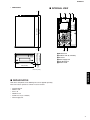
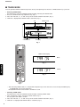
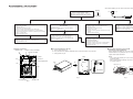
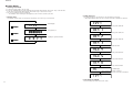
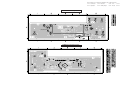
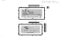
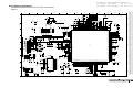
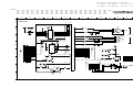
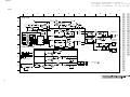
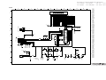
MICRO COMPONENT SYSTEM MCR-E810
DVD PLAYER
DVD-E810
SERVICE MANUAL
The MCR-E810 is composed of the DVD-E810, RX-E810 and NX-E800.
This service manual is for the DVD-E810.
For service manual of the RX-E810 and NX-E800, please refer to the following publication number:
RX-E810/RX-E410/NX-E800
101019
IMPORTANT NOTICE
This manual has been provided for the use of authorized YAMAHA Retailers and their service personnel.
It has been assumed that basic service procedures inherent to the industry, and more specifically YAMAHA Products, are already
known and understood by the users, and have therefore not been restated.
WARNING:
Failure to follow appropriate service and safety procedures when servicing this product may result in personal
injury, destruction of expensive components, and failure of the product to perform as specified. For these reasons,
we advise all YAMAHA product owners that any service required should be performed by an authorized
YAMAHA Retailer or the appointed service representative.
IMPORTANT: The presentation or sale of this manual to any individual or firm does not constitute authorization, certification or
recognition of any applicable technical capabilities, or establish a principle-agent relationship of any form.
The data provided is believed to be accurate and applicable to the unit(s) indicated on the cover. The research, engineering, and
service departments of YAMAHA are continually striving to improve YAMAHA products. Modifications are, therefore, inevitable
and specifications are subject to change without notice or obligation to retrofit. Should any discrepancy appear to exist, please
contact the distributor's Service Division.
WARNING:
Static discharges can destroy expensive components. Discharge any static electricity your body may have
accumulated by grounding yourself to the ground buss in the unit (heavy gauge black wires connect to this buss).
IMPORTANT: Turn the unit OFF during disassembly and part replacement. Recheck all work before you apply power to the unit.
DVD-E810
■ CONTENTS
TO SERVICE PERSONNEL ...................................... 2–3
PREVENTION OF ELECTROSTATIC DISCHARGE .... 4
LOCALE MANAGEMENT INFORMATION ................... 4
FRONT PANEL .............................................................. 5
REAR PANELS .............................................................. 5
SPECIFICATIONS ...................................................... 6–7
INTERNAL VIEW ........................................................... 7
REPAIR NOTES ............................................................. 7
TRADE MODE ................................................................ 8
101017
DISASSEMBLY PROCEDURES ................................... 9
TEST MODE ................................................................. 10
BLOCK DIAGRAM ....................................................... 11
WIRING DIAGRAM ...................................................... 12
PRINTED CIRCUIT BOARDS ................................ 13–16
SCHEMATIC DIAGRAMS ...................................... 17–22
REPLACEMENT PARTS LIST .............................. 24–25
SYSTEM CONTROL .............................................. 26–33
2006
All rights reserved.
This manual is copyrighted by YAMAHA and may not be copied or
redistributed either in print or electronically without permission.
P.O.Box 1, Hamamatsu, Japan
'06.08
DVD-E810
■ TO SERVICE PERSONNEL
WALL
OUTLET
1. Critical Components Information
Components having special characteristics are marked Z
and must be replaced with parts having specifications equal
to those originally installed.
2. Leakage Current Measurement (For 120V Models Only)
When service has been completed, it is imperative to verify
that all exposed conductive surfaces are properly insulated
from supply circuits.
●
Meter impedance should be equivalent to 1500 ohms shunted
by 0.15µF.
EQUIPMENT
UNDER TEST
AC LEAKAGE
TESTER OR
EQUIVALENT
INSULATING
TABLE
●
●
Leakage current must not exceed 0.5mA.
Be sure to test for leakage with the AC plug in both polarities.
WARNING: CHEMICAL CONTENT NOTICE!
The solder used in the production of this product contains LEAD. In addition, other electrical/electronic and/or plastic
(where applicable) components may also contain traces of chemicals found by the California Health and Welfare
Agency (and possibly other entities) to cause cancer and/or birth defects or other reproductive harm.
DO NOT PLACE SOLDER, ELECTRICAL/ELECTRONIC OR PLASTIC COMPONENTS IN YOUR MOUTH FOR ANY
REASON WHATSOEVER!
Avoid prolonged, unprotected contact between solder and your skin! When soldering, do not inhale solder fumes or
expose eyes to solder/flux vapor!
If you come in contact with solder or components located inside the enclosure of this product, wash your hands
before handling food.
WARNING: Laser Safety
This product contains a laser beam component. This component may emit invisible, as well as visible radiation,
which may cause eye damage. To protect your eyes and skin from laser radiation, the following precautions must be
used during servicing of the unit.
1) When testing and/or repairing any component within the product, keep your eyes and skin more than 30 cm away from
the laser pick-up unit at all times. Do not stare at the laser beam at any time.
2) Do not attempt to readjust, disassemble or repair the laser pick-up, unless noted elsewhere in this manual.
DVD-E810
3) CAUTION : Use of controls, adjustments or performance of procedures other than those specified herein may result in
hazardous radiation exposure.
Laser Emitting conditions:
1) When the Top Cover is removed, and the STANDBY/ON SW is turned to the "ON" position, the laser component will emit
a beam for several seconds to detect if a disc is present. During this time (5-10 sec.) the laser may radiate through the
lens of the laser pick-up unit. Do not attempt any servicing during this period!
If no disc is detected, the laser will stop emitting the beam. When a disc is loaded, you will not be exposed to any laser
emissions.
2) The laser power level can be adjusted with the VR on the pick-up PWB, however, this level has been set by the factory
prior to shipping from the factory. Do not adjust this laser level control unless instruction is provided elsewhere in this
manual. Adjustment of this control can increase the laser emission level from the device.
Laser Diode Properties
Type:
Wave length:
Output power:
Beam divergence:
2
Semiconductor laser GaAlAs
650 nm (DVD)
780 nm (VCD/CD)
7 mW (DVD)
10 mW (VCD/CD)
60 degree
DVD-E810
WARNING
CDX-497/CDX-397
Warning for power supply
The primary side of the power supply carries live mains voltage when the player is connected to the mains even when
the player is switched off !
This primary area is not shielded so it is possible to touch copper tracks and/or components when servicing the player.
Service personnel have to take precautions to prevent touching this area or components in this area.
DVD-E810
Note:
The screws on the DVD mechanism may never be touched, removed or re-adjusted.
Handle the DVD mechanism with care when the unit has to be exchanged!
The DVD mechanism is very sensitive for dropping or giving shocks.
3
DVD-E810
■ PREVENTION OF ELECTROSTATIC DISCHARGE
The laser diode in the DVD mechanism may be damaged due to static electricity from clothes or the human body. Use caution
to prevent electrostatic damage when servicing or handling the DVD-mechanism.
1. Grounding for electrostatic damage prevention
Some devices, such as the DVD player, use an optical pickup (laser diode) that will be damaged by static electricity in the
working environment. Only attempt service after ensuring that all grounding procedures have been completed.
1. Worktable grounding
Put a grounded conductive material (sheet) or iron sheet on the area where the optical pickup is placed.
2. Human body grounding
Use an anti-static wrist strap to discharge the static electricity from your body.
Anti-static wrist strap
1M-ohms
Conductive material
(sheet) or steel sheet
2. Handling Precautions for DVD mechanism
1. Handle the DVD mechanism gently, as it is an extremely high-precision assembly.
2. The flexible cable lines may break if an excessive force is applied to it. Use caution when handling the cable.
3. The semi-fixed resistor for laser power adjustment should not be adjusted. Do not turn the resistor.
■ LOCALE MANAGEMENT INFORMATION
DVD-E810
Locale Management Information : This DVD player is designed and manufactured to respond to the Locale
Management Information that is recorded on a DVD disc. If the Locale number described on the DVD disc does not
correspond to the Locale number of this DVD player, this DVD player cannot play this disc.
This product incorporates copyright protection technology that is protected by
method claims of certain U.S. patents and
other intellectual property rights owned by
Macrovision Corporation and other rights
owners. Use of this copyright protection
technology must be authorized by
Macrovision Corporation, and is intended
for home and other limited viewing uses
only unless otherwise authorized by
Macrovision Corporation. Reverse engineering or disassembly is prohibited.
5
2
1
6
3
5
4
2
4
2
5
4
DVD-E810
■ FRONT PANEL
DVD-E810 (U, C, T, K, A, B, G, L, V models)
■ REAR PANELS
DVD-E810 (A model)
DVD-E810 (T model)
DVD-E810 (B, G models)
CDX-497/CDX-397
DVD-E810 (U, C models)
DVD-E810
DVD-E810 (K, L, V models)
5
DVD-E810
■ SPECIFICATIONS
PLAYBACK SYSTEM
DVD Video, VR (Video Recording) format (DVD-RW)
Video CD & SVCD
CD
Picture CD
CD-R, CD-RW
DVD+R, DVD+RW, DVD+R DL
DVD-R, DVD-RW, DVD-R DL
GENERAL
Dimensions (W x H x D)
Weight
Finish
Power supply
VIDEO PERFORMANCE
Video (CVBS) output
1 Vpp into 75 ohms
S-Video output
Y: 1 Vpp into 75 ohms
C: 305 mVpp into 75 ohms
RGB (Scart) output
700 mVpp into 75 ohms
Component video output Y: 1 Vpp into 75 ohms
PB/CB PR/CR: 700 mVpp into 75 ohms
AUDIO FORMAT
Digital Dolby Digital/DTS/MPGE
Compressed Digital
PCM
16, 20, 24 bits
fs, 44.1, 48, 96 kHz
MP3 (ISO 9660) 96, 128, 256, 320 kbps
fs, 32, 44.1, 48 kHz
WMA
64 kbps to 192 kbps
fs, 44.1, 48 kHz
Analog sound
Stereo
AUDIO PERFORMANCE
DA converter
Signal to noise (1 kHz)
Dynamic range (1 kHz)
DVD
DVD-E810
24 bits/192 kHz
105 dB
97 dB
fs 96 kHz
2
fs 48 kHz
2
SVCD
fs 48 kHz
2
fs 44.1 kHz
2
CD/VCD
fs 44.1 kHz
2
Distortion and noise (1kHz) 0.0035 %
TV STANDARD
Number of lines
Playback
CONNECTIONS
SCART (B, G models)
Y output
PB/CB output
PR/CR output
S-Video output
Video output
Audio output (L+R)
Digital output
6
Hz
Hz
Hz
Hz
Hz
to
to
to
to
to
Power consumption
Standby power consumption
215 x 108 x 330 mm
(8-7/16" x 4-1/4" x 13")
2.3 Kg (5 lbs. 1 oz)
Gold color (T, A models)
Black color (G model)
Silver color
(U, K, B, G, L, V models)
AC 120 V, 60 Hz (U, C models)
AC 220 V, 50 Hz (T model)
AC 110-240 V, 50/60 Hz
(K, L, V models)
AC 240 V, 50 Hz (A model)
AC 230 V, 50 Hz (B, G models)
Approx. 12 W
< 1.0 W
ACCESSORIES
Power cable (1.8 m) x 1 (U, C models)
Power cable (1.5 m) x 1 (T, A, B, G models)
Power cable (1.5 m) x 3 (K, L, V models)
Audio pin cable (1.5 m) x 1
Video pin cable (1.5 m) x 1
* Specifications are subject to change without prior notice.
U ........ USA model
T ......... Chinese model
A ........ Australian model
G ........ European model
V ......... Taiwan model
44
22
22
20
20
kHz
kHz
kHz
kHz
kHz
(PAL/50 Hz) (NTSC/60 Hz)
625
525
Multistandard (PAL/NTSC)
Euroconnector
Cinch (green)
Cinch (blue)
Cinch (red)
Mini DIN, 4 pins
Cinch
Cinch
1 coaxial, 1 optical
IEC60958 for CDDA/LPCM
IEC61937 for MPEG 2, Dolby Digital
C ........
K ........
B ........
L ........
Canadian model
Korean model
British model
Singapore model
Manufactured under license from Dolby Laboratories. “Dolby” and the double-D symbol are
trademarks of Dolby Laboratories.
DivX, DivX Ultra Certified, and associated
logos are trademarks of DivX, Inc. and are
used under license.
DVD-E810
■ INTERNAL VIEW
7
321 (12-5/8")
3
4
330 (13")
108 (4-1/4")
(1/16")
2
2
5
6
1 MONO P.C.B.
2 SCART P.C.B. (B, G models)
3 AV P.C.B.
4 Power Supply Unit
5 DVD Mechanism
6 FRONT P.C.B.
8
(5/16")
100 (3-15/16")
1
CDX-497/CDX-397
215 (8-7/16")
(1/4")
• DIMENSIONS
Unit: mm (inch)
DVD-E810
■ REPAIR NOTES
None of the components of the following unit can be supplied separately.
Each unit must be replaced as a whole in case of a failure.
•
•
•
•
•
•
DVD Mechanism
MONO P.C.B.
AV P.C.B.
FRONT P.C.B.
SCART P.C.B. (B, G models)
Power Supply Unit
7
DVD-E810
■ TRADE MODE
This unit provides TRADE mode which prevents the tray from opening even when the “OPEN/CLOSE” key is pressed.
• Activating TRADE mode
The power to the main unit should be turned on before activating the TRADE mode.
1. Press the “OPEN/CLOSE” key to open the tray. (Fig. 1)
2. Press the “DVD/CD”, “2”, “5” and “9” keys on the remote control in that order. (Fig. 2)
3. “TRA ON” is displayed and TRADE mode is activated. (Fig. 3)
OPEN/CLOSE
Tray
STANDBY/ON
FL Display
Fig. 1
TRADE mode display
Enter
DVD-E810
Fig. 3
Cancel
Fig. 4
Fig. 2
* After activating TRADE mode, it is not possible to operate keys of the main unit as usual except the following key.
STANDBY/ON (Turn on the power only)
But operation with the remote control is available as usual.
• Canceling TRADE mode
The power to the main unit should be turned on before canceling TRADE mode.
1. Press and hold the “STOP” key on the remote control. (Fig. 2)
The tray opens after about 2 second.
2. Press the “DVD/CD”, “2”, “5” and “9” keys on the remote control in that order. (Fig. 2)
3. “TRA OFF” is displayed and TRADE mode is cancelled. (Fig. 4)
8
DVD-E810
■ DISASSEMBLY PROCEDURES
See REPLACEMENT PARTS LIST for item numbers.
When disassembling, use the special screw driver with tip shape in figure.
Mounting
Top Cabinet [240]
Remove 4 screws. [250] (4 on side)
Remove 4 screws. [251] (4 on rear side)
Lift top cabinet from rear side to remove.
Front Panel Ass'y [101]
Remove CN3 and 1800.
Open tray. (Fig. 2)
Unlock tray cover and close tray.
Remove 2 screws. (Front panel ass'y to side frame)
Remove 2 screws. [251] (Front panel ass'y to bottom frame)
Unlock front panel ass'y from frame by releasing successively 2
snaps. (2 on the side)
Remove front panel ass'y.
SCART P.C.B. [1003]
(B, G models)
Remove 1302.
Remove 2 screws. [260] (P.C.B. to rear panel)
Remove SCART P.C.B..
T10
2.7 mm
Dismounting
DVD Mechanism [1005]
Power Supply Unit [1006]
Solder the lauds of the optical pick up. (Fig. 3)
Open tray. (Fig. 2)
Unlock tray cover and close tray.
Remove 1101–1103.
Remove 4 screws. [52] (DVD mechanism to P.C.B.
support)
Remove DVD mechanism.
Remove CN101, CN1 and CN3.
Remove 2 screws. [251] (P.C.B. to bottom frame)
Release 2 spacers locking. (P.C.B. to bottom frame)
Remove power supply unit.
MONO P.C.B. [1004]
Solder the lauds of the optical pick up. (Fig. 3)
Remove 1101–1103, 1201, 1206 and 1207.
Remove 3 screws. [251] (P.C.B. to bracket A/B)
Remove MONO P.C.B..
FRONT P.C.B. [1001]
AV P.C.B. [1002]
Remove 4 screws. [251] (Bracket A/B to bottom frame)
Remove bracket A/B.
Remove 1800 and 1812.
Remove 2 screws. [251] (P.C.B. to bottom frame)
Remove 5 screws. [260] (P.C.B. to rear panel)
Remove AV P.C.B..
Remove 5 screws. [260] (P.C.B. to front panel ass'y)
Remove FRONT P.C.B..
Cable connections
How to manually eject the tray
MONO P.C.B.
a. Turn the player bottom up.
b. Move the slider in the direction indicated with a screw driver until the tray is ejected.
c. Gently pull the tray out.
SCART P.C.B. (B, G models)
1302 (B, G models)
CN101
1201
1207
1103
1102
1101
Preventive measure for laser diode
from electrostatic breakdown
When replacing the MONO P.C.B. or DVD mechanism, solder
between lands of the optical pick up P.C.B. to protect the laser diode
against electrostatic breakdown.
Rear
AV P.C.B.
1800
Power Supply Unit
Tray
1206
Bottom
a
b
Slider
1812
CN1
Notes
• Use an anti-static soldering iron to short-circuit and unshortcircuit laser diode.
• After you have finished repairing, remove the solder from the
short-circuit location.
Optical Pick Up
CN3
c
Screw Driver
Solder
Front
Fig. 2
DVD Mechanism
Fig. 3
FRONT P.C.B.
Fig. 1
9
DVD-E810
■ TEST MODE
• Starting Test Mode
a. Connect the power cable to the AC outlet.
b. Press the “STANDBY/ON” key while simultaneously pressing “NEXT/F.FWD” and “STOP” keys of the main unit.
At this time, keep pressing “NEXT/F.FWD” and “STOP” keys for 8 seconds or longer.
c. The “FV xx” (firmware version) is displayed.
* The firmware version and region code appears on the TV monitor screen at this time.
• Panel Key Test
• Display Test
The display condition varies as shown below according to the “PLAY” key of the main unit.
The display changes as shown below as the specified key is pressed.
* When performing the panel key test, a remote controller for RX-E810 is required.
Initial display
Press “OPEN/CLOSE” key of the main unit.
(OFF)
All segments on
Press “STANDBY/ON” key of the main unit.
(ON)
Lighting of segments in lattice
Press “OPEN/CLOSE” key of the main unit.
(OFF)
Press “STOP” key of the main unit.
Press “PLAY/PAUSE” key of the main unit.
Press “PREV/F.REV” key of the main unit.
Press “NEXT/F.FWD” key of the main unit.
Initial display
Press any key of the remote controller.
* Be sure to use a remote controller for RX-E810.
• Canceling Test Mode
10
Disconnect the power cable from the AC outlet.
A
B
C
D
E
F
G
H
I
J
DVD-E810
1
■ BLOCK DIAGRAM
AV
MONO
COAXIAL
Dual
Video
Amp
DIGITAL OUT
• See page 22 →
SCHEMATIC DIAGRAM
B, G models
• See page 19, 20 →
SCHEMATIC DIAGRAM
• See page 17, 18 →
SCHEMATIC DIAGRAM
7111
SCART
B,G,R
CVBS
AV
(SCART)
NJM2267M
2
OPTICAL
7102
216
7108
L78L05
Video
SW
B,G,R
IN
GND
OUT
TS5V330PW
B, G models
205,206
211
187
MCLK
AK4385ET
189
191
S-VIDEO
VIDEO OUT
3
COMPONENT
Y/PB/CB/PR/CR
182,183,185
6 CSN
DVM9.1
98
7 CCLK
99
8 CDTI
4
(Using MT 1389FXE chipset)
LRCK
2 BICK
3 SDTI
197
210
209
SD0
SCLK1
LRCK1
202
203
104
SYSCTR1
SYSCTRL2
uP
INTERFACE
14
VDD
DE-AMPHASIS
CONTROL
7209
1
MCLK
CLK
DIV.
DZFL
16
AOUTL+ 12
AUDIO DATA
INTERFACE
VIDEO
8x
INTERPOLATOR
MOD
SCF
AOUTL- 11
7204
5
6
7
3
2
1
AOUTR+ 10
8x
MOD
INTERPOLATOR
PDN
SCF
AUDIO OUT
L/R
AOUTR- 9
VSS
5
13
7120, 7123
7112
Tr. REG
+1V8
4
1801
109
7113
AV
STDBY
TO RX-E810
(SYSTEM CONNECTOR)
98
Tr. REG
+3V3
• See page 19, 20 →
SCHEMATIC DIAGRAM
99
Motor Driver
AM5888s
LGY3509-03xxF
100
7111
7103-7105
7100
7109
7-BT-299GNK
VS
OUT
Tray,
GND
Spindle
5
Motor
Power Supply Unit
7111
8
5,6
9
1105-1109
10-12
+12V
KEY1-3
6
uPD16312
DVD Mechanism
-12V
6111
41
+5V
FRONT
7
AV
• See page 19, 20 →
SCHEMATIC DIAGRAM
• See page 21 →
SCHEMATIC DIAGRAM
11
A
B
C
D
E
F
G
H
I
J
DVD-E810
1
■ WIRING DIAGRAM
AV (SCART)
1300
15FE-BT-VK-N
1809
SCART P.C.B.
1003
2
1
2
3
4
5
6
7
8
9
10
11
12
13
14
15
B, G models
1
2
3
4
5
6
7
8
9
10
11
12
13
14
15
8106
3140 110 20881
FFC 15P/120/15P AD
ANALOG L/R
OPT. SPDIF
1802
1803
COAX SPDIF
1804
YUV/CVBS
Y/C
1805
1806
A_L
GND
A_R
GND
P8_CTR
P16_CTR
GND
CVBS
GND
R
GND
G
GND
B
MUTE
MCLK 1
GND 2
BCLK 3
DAC_STB 4
LRCLK 5
GND 6
PCM_DATA0 7
SYS_CTRL1 8
SYS_CTRL2 9
GND 10
SPDIF 11
GND 12
CVBS 13
GND 14
Y_G 15
GND 16
B_Cb_Pb 17
GND 18
R_Cr_Pr 19
S0 20
S1 21
VSCK (SEL_0) 22
VSDA (SEL1) 23
MUTE_CTRL1 24
NC (MUTE_CTRL2) 25
GND 26
Y 27
GND 28
C 29
GND 30
1002
AV P.C.B.
Power Supply Unit
3
1006
JST EH
CN1
+5Vstby
GND
+5Vstby
GND
+12VA
+5Vstby
-12VA
STBY_PSU
1
2
3
4
5
6
7
8
30FE-BT-VK-N
30FE-BT-VK-N
1807
2P JST-VA/VH
8107
3139 241 01731
CABLE 2P/140
A_L
GND
A_R
GND
P8_CTR
P16_CTR
GND
CVBS
GND
R
15FE-BT-VK-N
GND
1302
G
GND
B
MUTE
SYS_CTRL
1801
1201
8100
3139 111 04121
FFC 30P/120/30P AD
1
2
3
4
5
6
7
8
9
10
11
12
13
14
15
16
17
18
19
20
21
22
23
24
25
26
27
28
29
30
MCLK
GND
BCLK
DAC_STB
LRCLK
GND
PCM_DATA0
SYS_CTRL1
SYS_CTRL2
GND
SPDIF
GND
CVBS
GND
Y_G
GND
B_Cb_Pb
GND
R_Cr_Pr
S0
S1
VSCK (SEL_0)
VSDA (SEL1)
MUTE_CTRL1
NC (MUTE_CTRL2)
GND
Y
GND
C
GND
1004
MONO P.C.B.
DVM9.1
JST EH
1812
EH 1207
1
2
3
4
5
6
7
8
8P/140/8P
+5Vstby
GND
+5Vstby
GND
+12VA
+5Vstby
-12VA
STBY_PSU
+5VL
GND
GND
+5STBY
STBY_PSU
1
2
3
4
5
PH 1206
+5Vstby
VSDA
VSCK
VSTB
GND
IR
PCB_LRCLK
+5VL
STBY_FRONT
LOAD+
LOADTROUT
GND
TRIN
1
2
3
4
5
PH 1103
SLEDSLED+
1
2
3
4
5
6
SP+
SPL_SW
GND
GND-LD
LD-DVD
NC
HFM
MD
LD-CD
VR-DVD
VR-CD
NC
E
VCC
Vc
GND-PD
F
B
A
RF
CD/DVD
D
C
TT+
F+
F1
2
3
4
5
6
7
8
9
10
11
12
13
14
15
16
17
18
19
20
21
22
23
24
05P/280/05P
06P/220/06P
8009
05P/280/05P
5
PH 1813
3139 241 100391
FFC 24P/280/24P AD
0.5mmP
PH 1800
PH 1102
EH 1811
1101
+5VL
GND
GND
+5Vstby
STBY_PSU
1
2
3
4
5
SFW24R-2STE 1
VSDA
VSCK
VSTB
GND
IR
PCB_LRCLK
+5VL
STBY_FRONT
+5Vstby
1
2
3
4
5
6
7
8
9
VSDA
VSCK
VSTB
GND
IR
PCB_LRCLK
+5VL
STBY_FRONT
+5Vstby
1
2
3
4
5
6
7
8
9
1
2
3
4
5
CN3
JST EH
GND
+12VA
GND
+5Vstby
-24V
4
6
VSDA
VSCK
VSTB
GND
IR
PCB_LRCLK
+5VL
STBY_FRONT
1005
DVD Mechanism
(WXD8829 + KHM-313)
1
2
3
4
5
6
7
8
9
FRONT P.C.B.
+5Vstby
1001
PH 1103
09P/280/09P
09P/100/09P
7
05P/100/05P
12
1
2
3
4
5
LOAD+
LOADTROUT
GND
TRIN
SLEDSLED+
1
2
3
4
5
6
SP+
SPL_SW
GND
1
2
3
4
5
6
7
8
9
10
11
12
13
14
15
16
17
18
19
20
21
22
23
24
GND-LD
LD-DVD
NC
HFM
MD
LD-CD
VR-DVD
VR-CD
NC
E
VCC
Vc
GND-PD
F
B
A
RF
CD/DVD
D
C
TT+
F+
F-
GND
+12VA
GND
+5Vstby
-24V
1
2
3
4
5
SFW24R-2STE 1
EH 1100
1
2
3
4
5
6
7
8
9
DVD-E810
The first digit of a component indicates the component type.
1xxx : Connector
2xxx : Capacitor
■ PRINTED CIRCUIT BOARDS
3xxx : Resistor
4xxx : SMD jumper
5xxx : Coil
6xxx : Diode
7xxx : IC, Transistor, FET
9xxx : Wire jumper
FOR INFORMATION ONLY (NO SERVICE PARTS WILL BE AVAILABLE)
MONO P.C.B. Bottom View
AV P.C.B. (1813)
Page 14
A
3
AV P.C.B. (1811)
Page 14
A
3
AV P.C.B. (1807)
Page 14
B
2
MONO P.C.B. Top View
DVD Mechanism
13
DVD-E810
The first digit of a component indicates the component type.
1xxx : Connector
2xxx : Capacitor
AV P.C.B. Top View
VIDEO OUT
COMPONENT
S-VIDEO
PR
VIDEO
MONO P.C.B. (1206)
3
Page 13 C
Power Supply Unit (CN1)
14
U, C, T, K, A, L, V models
Y
PB
B, G models
MOMO P.C.B. (1207)
3
Page 13 C
FRONT P.C.B. (1103)
SCART P.C.B. (1302)
4
1
Page 15 A
Page 16 A
COAXIAL
7xxx : IC, Transistor, FET
9xxx : Wire jumper
B, G models
DIGITAL OUT
OPTICAL
5xxx : Coil
6xxx : Diode
AV P.C.B. Bottom View
MONO P.C.B. (1201)
1
Page 13 A
TO RX-E810 AUDIO
(System Connector) OUT
L/R
3xxx : Resistor
4xxx : SMD jumper
DVD-E810
The first digit of a component indicates the component type.
1xxx : Connector
2xxx : Capacitor
3xxx : Resistor
4xxx : SMD jumper
5xxx : Coil
6xxx : Diode
7xxx : IC, Transistor, FET
9xxx : Wire jumper
FRONT P.C.B. Top View
PROGRESSIVE
STANDBY/ON
AV P.C.B. (1800)
3
Page 14 A
Power Supply Unit (CN3)
FRONT P.C.B. Bottom View
15
DVD-E810
The first digit of a component indicates the component type.
1xxx : Connector
2xxx : Capacitor
SCART P.C.B. Top View
(B, G models)
AV P.C.B. (1809)
2
Page 14 A
AV (SCART)
SCART P.C.B. Bottom View
16
(B, G models)
3xxx : Resistor
4xxx : SMD jumper
5xxx : Coil
6xxx : Diode
7xxx : IC, Transistor, FET
9xxx : Wire jumper
DVD-E810
The first digit of a component indicates the component type.
1xxx : Connector
2xxx : Capacitor
■ SCHEMATIC DIAGRAMS
3xxx : Resistor
4xxx : SMD jumper
5xxx : Coil
6xxx : Diode
7xxx : IC, Transistor, FET
9xxx : Wire jumper
FOR INFORMATION ONLY (NO SERVICE PARTS WILL BE AVAILABLE)
MONO 1/2
9
10
11
12
2133
IOA
100n
+5M
2138
+V18
6
TRCLOSE
10K
3150
7
TROPEN
2
TRB1
D
D
25
TRB2
1103
B5B-PH-K
27
V1P4
4133
28
STBY
LOAD-
4138
+
VOSL
+
VOLD
FWD
-
REV
+
VOTK
-
1
TRB
+
2
VOTR
-
BIAS
1
MUTE
REGO
20
4147
22p
22p
22p
22p
22p
TRIN
GND
DV33
3157
TROUT
3158
SL+
18
SL-
15
T-
16
T+
10
LOAD+
9
LOAD-
6105
1N4001
TRB2
TRB1
PSS8550
7113
4K7
4K7
2113
100n
3179
47R
S0
3180
47R
S1
HDMI_C2
HDMI_C3
HDMI_C4
DV33
HDMI_C5
HDMI_C6
HDMI_C7
HDMI_VCK
HDMI_Y0
HDMI_Y1
HDMI_Y2
HDMI_Y3
HDMI_Y4
2116
100n
E
+V18
HDMI_Y5
HDMI_Y6
HDMI_Y7
2128
100n
DV33
MA4
MA5
MA6
MA7
MA8
MA9
MA11
2130
100n
D
F
DCKE
DCLK
2134
100n
MA3
MA2
DV33
+V18
MA1
MA0
MA10
BA1
BA0
CS
RAS
CAS
WE
DQM1
LIMIT
DQ8
2137
100n
D
G
DV33
UP3_1
22R
3162
UP3_0
22R
3164
STBY_PSU
STBY_FRONT
100n
560R
2177
3119
PCM_DATA0
H
DV33
D
5
REGO1
3
REGO2
+V18
+1V8
DV33
15K
3154
5K6
3153
REGO1
REGO2
9K1
3160
10K
D
3159
100n
2151
DV33
D
D
DV33
VSCK
VSDA
VSTB
100n
2155
3174
3175
3176
47R
47R
47R
7114
NCP303LSN30
1
INP
OUTP
GND NC
CD
TRIN
2
+5D
I
5
2159
100n
1
2
3
4
D
1
2
3
4
D
+V18
D
D
D
PSS8550
7112
PGND
D
4136
+5V_STBY
3
4K7
D
SP-
17
NC
D
4K7
SP+
2148
I
10K
3155
24
2
22
100n
TROUT
F-
11
12
VINTK
VTCL
13
D
4
H
100n
2144
10K
-
VINLD
F+
3152
21
VINSL+
14
HDMI_RST
HDMI_C0
HDMI_C1
2146
26
3149
+
VOFC
2109
100n
#Y_G
#B_Cb_Pb
#R_Cr_Pr
D
23
TRSO
OP-
OP+
10K
DV33
10K
FMSO
MOTOR DRIVER
VINFC
65
66
67
68
69
70
71
72
73
74
75
76
77
78
79
80
81
82
83
84
85
86
87
88
89
90
91
92
93
94
95
96
97
98
99
100
101
102
103
104
105
106
107
108
109
110
111
112
113
114
115
116
117
118
119
120
121
122
123
124
125
126
127
128
3147
150K
4
DMSO
+5M
VCC
A(2)
A(3)
A(4)
A(5)
A(6)
A(7)
A(8)
A(18)
A(19)
100n
Φ
2141
100n
2140
100n
6104
3146
150K
3145
1
FOSO
3148
19
8
7111
AM5888S
1R0
30
3143
5157
BLM18P
47u 16V
1N4001
50R
SP-
DV33
SP+
D
SL-
ADIN
TROUT
TRIN
STBY
TRCLOSE
+5M
2199
5159
BLM31
+V_V33
#CVBS
DV33
100n
+5V_STBY 50R
SL+
4130
T155
T156
T157
T158
22p
C
#C
DQ2
DQ1
DQ0
DQ15
DQ14
DQ13
DQ12
DQ11
DQ10
DQ9
2131
100n
2195
100n
#Y
100n
5155
BLM18P
DQM0
IOA
DQ7
DQ6
DQ5
DQ4
DQ3
DV33
192
191
190
189
188
187
186
185
184
183
182
181
180
179
178
177
176
175
174
173
172
171
170
169
168
167
166
165
164
163
162
161
160
159
158
157
156
155
154
153
152
151
150
149
148
147
146
145
144
143
142
141
140
139
138
137
136
135
134
133
132
131
130
129
4K7
3139
470R
7109
BC817-25W
DMO
FMO
TROPEN
T137
TRO
FOO
7108
MT1389
3151
680K
2n2
T136
T138
RC6
OPOP+
V1P4
100n
A(17)
A(0)
3138
2129
2126
D
2123
2124
2122
680K
100n
47u
100n
100n
47u
2121
2120
2119
+RF_V5
2n2
3135
220u
2
2125
T112
T139
T140
V2P8
V20
V1P4
AD(7)
100n
100n
2188
2114
47u 16V
2117
2118
T141
T142
6n8
1
5156
2002
4127
22p
BLM18P
2132
V20
V2P8
100n
47u
3
25
2185
V1P4
1
47u 16V
2115
3137
470R
3140 10K
D_
C_
TT+
F+
F-
T125
T126
T127
T128
T129
T130
100n
5154
PWR
A(16)
A(15)
A(14)
A(13)
A(12)
A(11)
A(10)
A(9)
A(20)
PCE
A(1)
PRD
AD(0)
AD(1)
2
3
2
3
1
3136
470R
F
B_
A_
BC847B
7107
BC847B
7106
2127
100n
V20
T113
T114
T115
T116
T117
T118
T119
T120
T121
T122
T123
2136
2139
2160
2162
2163
DV33
E
LIMIT
2142
4126
ADIN
T109
T110
T111
T131
T132
T133
T134
T135
E
F
3134
100R
3133
100R
5158
1
2
3
4
5
5148
BLM18P
DV33
7104
BC807-25
29
G
7105
BC807-25
3132
390R
T103
T104
T105
T106
T107
1102
B6B-PH-K
6
5
4
3
2
1
3130
4R7 +L_V33
+L_V33
B
+V_V33
YUV0
FS
VREF
DACVDDC
RD16
RD17
RD18
RD19
RD20
RD21
DVDD3_8
RD22
RD23
DQM2
DQM3
RD24
RD25
DVSS_11
RD26
DVDD18_5
RD27
RD28
RD29
RD30
RD31
DVDD3_7
RA4
RA5
RA6
DVSS_10
RA7
DVSS_9
RA8
RA9
RA11
CKE
RCLK
DVDD3_6
RCLKB
RVREF
DVDD18_4
RA3
RA2
RA1
DVSS_8
RA0
RA10
BA1
DVSS_7
BA0
RCS#
DVDD3_5
RAS#
CAS#
RWE#
DQM1
DQS1
RD8
DVSS_6
RD9
RD10
RD11
RD12
RD13
UP3_0
UP3_1
15n
2108
100n
330p
2107
2106
330p
2105
2112
100n
2111
220u
T101
T102
1
2
3
4
5
6
7
8
9
10
11
12
13
14
15
16
rf 17
18
19
20
21
22
23
24
26
F
3131
4R7
5153
10u
5152
BLM18P
1101
SFV24R-1ST
E
5151
10u
T143
4122
4123
4124
4125
V1P4
AGND
DVDA
DVDB
DVDC
DVDD
DVDRFIP
DVDRFIN
MA
MB
MC
MD
SA
SB
SC
SD
CDFON
CDFOP
TNI
TPI
MDI1
MDI2
LDO2
LDO1
SVDD3
CSO
RFLVL
SGND
V2REFO
V20
VREFO
FEO
TEO
TEZISLV
OP_OUT
OP_INN
OP_INP
DMO
FMO
TROPENPWM
PWMOUT1
TRO
FOO
USB_VSS
USBP
USBM
USB_VDD3
FG
TDI
TMS
TCK
TDO
DVDD18_1
IOA2
IOA3
IOA4
IOA5
IOA6
IOA7
HIGHA0
IOA18
IOA19
DVSS_1
APLLCAP
APLLVSS
AD(2)
AD(3)
AD(4)
AD(5)
AD(6)
A21
DMO
10K
1
2
3
4
5
6
7
8
9
10
11
12
13
14
15
16
17
18
19
20
21
22
23
24
25
26
27
28
29
30
31
32
33
34
35
36
37
38
39
40
41
42
43
44
45
46
47
48
49
50
51
52
53
54
55
56
57
58
59
60
61
62
63
64
1u0
1u0
1u0
1u0
1u0
2145
2186
3126
DMSO
2196
2197
2102
2103
2104
C_
B_
A_
D_
APLLVDD3
IOWR#
A16
HIGHA7
HIGHA6
HIGHA5
HIGHA4
HIGHA3
DVDD3_1
HIGHA2
HIGHA1
IOA20
IOCS#
IOA1
IOOE#
DVDD3_2
AD0
AD1
AD2
AD3
DVSS_2
AD4
AD5
AD6
IOA21
ALE
AD7
A17
IOA0
DVSS_3
UWR#
URD#
DVDD18_2
UP1_2
UP1_3
UP1_4
UP1_5
UP1_6
UP1_7
UP3_0
UP3_1
UP3_4
UP3_5
DVDD3_3
ICE
PRST#
IR
INT0#
DQM0
DQS0
RD7
DVSS_4
RD6
RD5
DVSS_5
RD4
RD3
DVDD18_3
RD2
RD1
RD0
RD15
DVDD3_4
RD14
FMO
15K
2187
100n
To DVD Mechanism
27K
3125
FMSO
+RF_V5
AVDD3
IREF
RFGC
OSN
OSP
CEQN
CEQP
RFGND
CRTPLP
HRFZC
RFRPAC
RFRPDC
RFVDD3
S_VREFN
S_VREFP
ADCVSS
S_VCM
ADCVDD3
LPFOP
LPFIN
LPFIP
LPFON
PLLVDD3
IDACEXLP
PLLVSS
JITFN
JITFO
XTALI
XTALO
RFVDD18
RFGND18
SPDIF
MC_DATA
DVSS_13
ASDATA4
DVDD18_6
ASDATA3
ASDATA2
ASDATA1
ASDATA0
DVSS_12
ACLK
ABCK
ALRCK
DVDD3_10
SPBCK
SPLRCK
SPDATA
SPMCLK
HSYN
YUV7
VSYN
DVDD3_9
YUV6
YUV5
DACVSSA
YUV4
DACVDDA
YUV3
DACVSSB
YUV2
DACVDDB
YUV1
DACVSSC
TRO
2184
100n
2143
2194
2n2
2193
100n
3124
DV33
2001
100u
FOO
27K
100n
+RF_V5
+5VL
RFVDD
3123
FOSO
TRSO
D
SPMCLK
PCM_DATA2
PCM_DATA1
5160
BLM18P
5147
BLM18P
203
202
201
200
199
198
197
196
195
194
193
2192
RFVDD
DV33
5145
BLM18P
C
100K
2165
22p
2158
2164
22p
5141
2169
100n
3117
V1P4
XTALI
B
+V_V33
+V18
+V_V33
33R
3166
100K
2161
3116
22p
2166
1n0
10u
2154
3
1
3
100n
220u
4
NC
1
NC
+V18
100n
5
5
5140
BLM18P
+1V8
SubW
100n
7116
74HC1G04GW
4
2
1
A
SurrR
+V_V33
100n
7115
74HC1G04GW
2
1
DV33
MUTE_CTRL2
2152
I2C_DAT
I2C_CLK
Ro
RFVDD
2101
A
3104
Lo
DV33
14
DV33
SurrL
3105
256
3120
15K
255
100n
254
2178
2179
100n
253
252
251
2180
33n
250
2181 100n
249
248
247
246
2176
100n
245
RFVDD
244
10V
2167
100u
243
2182 47n
242
2168 100n
241
2183 47n
240
5142
239
3112
6R8
2149 470n
238
BLM18P
237
236
2170
1n0
2150
10u
235
3118
750K
234
XTALI
233
BLM18P
5144
+V18
XO
2171 100n
232
231
5139
60R
DV33
10V 100u
2153
230
6.3V 4u7 2172
229
228
227
226
225
2189 6.3V 10u
224
223
222
221
2174 6.3V 10u
220
219
5143
60R
DV33
10V 100u
2173
218
217
2175 100n
216 33R
3121
SPDIF_OUT
215 33R
3122
AUX_DATA_IN
214 33R
3165
PCM_DATA4
213
2156 100n
212
PCM_DATA3
211
PCM_MCLK
210
PCM_BCLK
100n
209
2157
PCM_LRCLK
208
DV33
207
SPBCLK
MUTE_CTRL1
22R
206
3178
SPLRCLK
205
SPDATA
22R
3181
204
CENTRE_CH
13
2190
8
2191
7
D
6
DV33
5
100n
4
100n
3
2003
2
10K
1
5
6
D
DV33
1104
B4B-PH-K
7
8
9
10
11
12
13
1101 D1
1102 F1
1103 H1
1104 I10
2001 B6
2002 F2
2003 I13
2101 A4
2102 C6
2103 C6
2104 C6
2105 C3
2106 C4
2107 C4
2108 C4
2109 C14
2111 D2
2112 D2
2113 D13
2114 D5
2115 D3
2116 E13
2117 E5
2118 E5
2119 E4
2120 E4
2121 E4
2122 E4
2123 E4
2124 E5
2125 E5
2126 E6
2127 E2
2128 E13
2129 E5
2130 F13
2131 F6
2132 F6
2133 F3
2134 F13
2136 I1
2137 G13
2138 G4
2139 I1
2140 G6
2141 G6
2142 G1
2143 G13
2144 H3
2145 H7
2146 I11
2148 I4
2149 A9
2150 A9
2151 I9
2152 A8
2153 A9
2154 A8
2155 I9
2156 B10
2157 B11
2158 B2
2159 I12
2160 I1
2161 B2
2162 I1
2163 I1
2164 B4
2165 B5
2166 A8
2167 B8
2168 B8
2169 A13
2170 B9
2171 B9
2172 A9
2173 B10
2174 B10
2175 B10
2176 B8
2177 B12
2178 B8
2179 B8
2180 B8
2181 B8
2182 B8
2183 B8
2184 B12
2185 G1
2186 C2
2187 I8
2188 I8
2189 B10
2190 B13
2191 B13
2192 B7
2193 B6
2194 B6
2195 C13
2196 C6
2197 C6
2199 G3
3104 A12
3105 A12
3112 A9
3116 B4
3117 B8
3118 B9
3119 B12
3120 B7
3121 B10
3122 B10
3123 B4
3124 C4
3125 C4
3129 D14
3130 D5
3131 D3
3132 D2
3133 E3
3134 E3
3135 E5
3136 E2
3137 E3
3138 E5
3139 F3
3140 F3
3143 G2
3145 G2
3146 G2
3147 G2
3148 G3
3149 H3
3150 H3
3151 H10
3152 I12
3153 I6
3154 I7
3155 I3
3157 I3
3158 I3
3159 I6
3160 I7
3162 H13
3164 H13
3165 B10
3166 A5
3174 I9
3175 I9
3176 I9
3178 B11
3179 D14
3180 D14
3183 F7
4122 C7
4123 C7
4124 C7
4125 D7
4126 D7
4127 F2
4130 G2
4133 I2
4136 H7
4138 I2
4147 I2
5139 A9
5140 A2
5141 B4
5142 A9
5143 B10
5144 A9
5145 B2
5147 B13
5148 D5
5151 D3
5152 D2
5153 D3
5154 E5
5155 F6
5156 F3
5157 G6
5158 G1
5159 G3
5160 B6
6104 H7
6105 H6
7104 D4
7105 D3
7106 E2
7107 E3
7108 E10
7109 F3
7111 G4
7112 H6
7113 H7
7114 I11
7115 A4
7116 A5
T101 D2
T102 D2
T103 E2
T104 E2
T105 E2
T106 E2
T107 E2
T109 E2
T110 E2
T111 E2
T112 E7
T113 E2
T114 E2
T115 E2
T116 E2
T117 F2
T118 F2
T119 F2
T120 F2
T121 F2
T122 F2
T123 F2
T125 G1
T126 G1
T127 G1
T128 G1
T129 G1
T130 G1
T131 I1
T132 I1
T133 I1
T134 I1
T135 I1
T136 E7
T137 F7
T138 E7
T139 E7
T140 E7
T141 E7
T142 E7
T143 C7
T155 I10
T156 I10
T157 I10
T158 I10
14
17
DVD-E810
The first digit of a component indicates the component type.
1xxx : Connector
2xxx : Capacitor
3xxx : Resistor
4xxx : SMD jumper
5xxx : Coil
6xxx : Diode
7xxx : IC, Transistor, FET
9xxx : Wire jumper
MONO 2/2
1
2
R_Cr_Pr
5
3204
150R
2204
47p
5202
1u8
6
7
To 1807 of AV P.C.B.
Page 19
C
2203
47p
3203
150R
2202
47p
5201
1u8
4
#C
3202
150R
2201
47p
#R_Cr_Pr
3201
150R
3
8
9
To 1813 of AV P.C.B.
Page 19
1
F
10
11
12
13
10
F
+5V_STBY
D
B9B-PH-K
1206
#Y
VSDA
VSCK
VSTB
Y
5204
1u8
4203
PCM_LRCLK
3209
150R
3208
150R
3207
150R
2205
47p
5203
1u8
2206
47p
B_Cb_Pb
2208
47p
#B_Cb_Pb
3206
150R
F249
F222
F223
F224
F225
F226
F227
F228
F229
D
D
2207
47p
A
1K0
RC6
4206
3205
+5VL
22R
22R
3277
3278
30
29
28
27
26
25
24
23
22
21
20
19
18
17
16
15
14
13
12
11
10
9
8
7
6
5
4
3
2
1
F201
MUTE_CTRL2
F202
B
F203
F204
F205
F206
F207
F208
F209
SEL_1
SEL_0
S1
S0
3213
150R
2212
47p
2211
47p
3212
150R
CVBS
5206
1u8
F210
F211
F212
D
C
F213
PCM_DATA0
PCM_LRCLK
4216
PCM_BCLK
3267
33R
3217
33R
3218
33R
F214
F215
F216
F217
F218
F219
F221
F220
AUX_DATA_IN
3221
3281
DV33
D
1207
22p
22p
22p
22p
22p
22p
2221
2222
2223
2224
2225
2226
+5VL
F246
+5V_STBY
STBY_PSU
F247
F248
1
2
3
4
5
22p
22p
B5B-EH-A
B
2235
2236
D
D
D
To 1811 of AV P.C.B.
Page 20
7
E
C
5207
BLM18P
7201
74HC1G125GW
3219
1K0
DV33
5
2213
100n
3220
22R
D
2
SPDIF_OUT
4
1
HDMI_AUDIO_MUTE
#SPDIF_OUT
EN
3
1201
2268
D
D
DV33
1K0
3258
100n
8
7212
M24C16-RDW6
(2Kx8)
EEPROM
D
1
2
3
0
1
2
WC
SCL
ADR
SDA
7
6
5
I2C_CLK
E
I2C_DAT
4
E
D
Φ
D
2220 22p
D
3225
1K0
2219 22p
3224
1K0
3223
3
7214
74AHC1G125GW
2217 22p
EN
2218 22p
1
3222
2216 22p
4 33R
2215 22p
2
2214 22p
PCM_MCLK
#PCM_MCLK
#PCM_BCLK
#PCM_LRCLK
#PCM_DATA0
#PCM_DATA1
#PCM_DATA2
#SPDIF_OUT
D
2230
2231
2232
2234
5
100n
22p
22p
22p
A
4209
STBY_FRONT
4213
2210
47p
3211
150R
2209
47p
3210
150R
VSDA
VSCK
MUTE_CTRL1
D #CVBS
2227
2228
2229
30FE-BT-VK-N
Y_G
5205
1u8
22p
22p
22p
D
D
D
#Y_G
1
2
3
4
5
6
7
8
9
5211
BLM18P
150R
150R
150R
150R
150R
150R
150R
150R
150R
150R
150R
150R
23
24
25
26
29
30
31
32
33
34
22
35
BA0
BA1
3251
3252
150R
150R
20
21
VDD
0
1
2
3
4
5 A 0
1M-1
6
7
8
9
10
11
49
43
VDDQ
NC
1M X 16 X 4
0
1
2
3
4
5
6
7
8
9
10
11
12
13
14
15
7206
IS42S16400A
D
47R
150R
150R
150R
150R
150R
38
37
19
18
17
16
CLK
CKE
CS
RAS
CAS
WE
1
2
6
VSSQ
54
H
41
28
VSS
3
DQM
H
L
36
40
2
4
5
7
8
10
11
13
42
44
45
47
48
50
51
53
39
15
DQ7
DQ6
DQ5
DQ4
DQ3
DQ2
DQ1
DQ0
DQ8
DQ9
DQ10
DQ11
DQ12
DQ13
DQ14
DQ15
3263
3264
25
24
23
22
21
20
19
18
8
7
6
5
4
3
2
1
48
17
16
9
150R
150R
DQM1
DQM0
RB
RP
WE
OE
CE
BYTE
+3V3_FL
PWR
PRD
PCE
+3V3_FL
3257
4
5
10K
47u
2247
100n
16V
37
0
[FLASH]
1
2Mx8/1Mx16
2
3
4
5
6
7
8
0
9
A
10
2M-1 / 1M-1
11
12
13
14
15
16
17
18
19
0
1
2
3
4
5
6
7
D
8
9
10
11
12
13
14
15
A-1
NC
52
3253
3254
3256
3270
3259
3261
46
DCLK
DCKE
CS
RAS
CAS
WE
0
BA
1
12
G
18
9
3
27
Φ
DRAM
VDD
A(1)
A(2)
A(3)
A(4)
A(5)
A(6)
A(7)
A(8)
A(9)
A(10)
A(11)
A(12)
A(13)
A(14)
A(15)
A(16)
A(17)
A(18)
A(19)
A(20) 4210
D
DV33
2244
29
31
33
35
38
40
42
44
30
32
34
36
39
41
43
45
13
14
10
AD(0:7)
3233
3235
3237
3239
3240
3241
3242
3244
3246
3248
3249
3250
7205
M29W160ET70
AD(0)
AD(1)
AD(2)
AD(3)
AD(4)
AD(5)
AD(6)
AD(7)
F
A(0)
G
3255
22R
+3V3_FL
A21
VSS
46
MA0
MA1
MA2
MA3
MA4
MA5
MA6
MA7
MA8
MA9
MA10
MA11
+3V3_FL
100n
100n
100n
100n
100n
100n
100n
A(0:21)
F
14
1
2241
47u 16V
2240
2242
2243
2245
2246
2248
2249
27
DV33
5212
BLM18P
6
H
7
8
9
10
11
12
13
1201 D5
1206 A8
1207 B8
2201 A1
2202 A1
2203 A3
2204 A3
2205 A1
2206 A1
2207 A3
2208 A3
2209 B1
2210 B1
2211 B1
2212 B1
2213 C8
2214 D3
2215 D3
2216 D3
2217 D3
2218 D3
2219 D4
2220 D4
2221 B6
2222 B6
2223 B6
2224 B6
2225 B6
2226 B6
2227 A9
2228 A9
2229 A9
2230 A9
2231 A9
2232 A9
2234 A9
2235 B9
2236 B9
2240 E3
2241 E2
2242 E3
2243 F3
2244 F7
2245 F3
2246 F3
2247 F7
2248 F3
2249 F3
2268 D2
3201 A1
3202 A2
3203 A3
3204 A4
3205 A7
3206 A1
3207 A2
3208 A3
3209 A4
3210 B1
3211 B2
3212 B1
3213 B2
3217 C2
3218 C2
3219 C6
3220 C8
3221 D2
3222 D2
3223 D4
3224 D4
3225 D4
3233 F2
3235 F2
3237 F2
3239 F2
3240 F2
3241 F2
3242 F2
3244 G2
3246 G2
3248 G2
3249 G2
3250 G2
3251 G2
3252 G2
3253 G2
3254 G2
3255 G7
3256 G2
3257 H5
3258 D12
3259 H2
3261 H2
3263 H4
3264 H4
3267 D1
3270 H2
3277 B3
3278 B3
3281 D4
4203 A7
4206 A6
4209 B7
4210 G5
4213 D7
4216 D1
5201 A1
5202 A3
5203 A1
5204 A3
5205 B1
5206 B1
5207 C8
5211 E2
5212 E7
7201 C7
7205 E5
7206 G3
7212 D11
7214 D2
F201 B5
F202 B5
F203 B5
F204 B5
F205 B5
F206 B5
F207 B5
F208 B5
F209 B5
F210 C5
F211 C5
F212 C5
F213 C5
F214 C5
F215 C5
F216 C5
F217 C5
F218 D5
F219 D5
F220 D5
F221 D5
F222 A8
F223 A8
F224 A8
F225 A8
F226 A8
F227 A8
F228 A8
F229 A8
F246 B8
F247 B8
F248 B8
F249 A8
DVD-E810
The first digit of a component indicates the component type.
1xxx : Connector
2xxx : Capacitor
3xxx : Resistor
4xxx : SMD jumper
5xxx : Coil
6xxx : Diode
7xxx : IC, Transistor, FET
9xxx : Wire jumper
AV 1/2
1800 F9
1801 G13
1805 C12
1806 B12
1807 F1
1809 D9
2105 B2
2106 B2
2107 B10
2109 C9
2110 C8
2114 C8
1813 F10
2100 B4
2101 B2
2102 B2
2103 B8
2104 B8
1
A
2115 C9
2117 D9
2118 D8
2121 D9
2122 D8
2125 D5
3103 B3
3112 C8
3147 D3
3149 D6
3150 E6
3160 E4
2130 F4
2131 F11
2132 G11
2133 D4
2134 B8
2135 F12
2
3165 G3
3167 F4
3173 G4
3175 F4
3176 G3
3182 F4
3
3198 E11
4100 B6
4101 B6
4102 B6
4116 D5
4119 F12
3192 E10
3193 F10
3194 G10
3195 G11
3196 D12
3197 E11
3184 G5
3187 G4
3188 G6
3189 H4
3190 G5
3191 E10
4
5
5100 B2
5101 B2
5103 G11
7102 B4
7111 D4
7118 F4
T100 F2
T101 F2
T102 D2
T103 F2
T104 F2
T107 E2
7119 F5
7120-1 E11
7120-2 E11
7122-1 H5
7122-2 H5
7123 F12
6
7
T122 B9
T123 B9
T124 C10
T125 D10
T126 C10
T128 B11
T114 E2
T115 E2
T116 D2
T118 D2
T119 D2
T121 C10
T108 E2
T109 E2
T110 E2
T111 E2
T112 E2
T113 E2
8
T135 E8
T136 E8
T137 F8
T138 F8
T141 F2
T142 F2
T129 D8
T130 E8
T131 E8
T132 E8
T133 E8
T134 E8
9
T153 G12
T154 G12
T143 F2
T144 B2
T145 B2
T150 G12
T151 G10
T152 G10
10
11
12
13
14
VIDEO PART
A
B|U
G|Y
R|V
4100
4101
4102
U, C, T, K, A, L, V models
+5VA
B, G models
2100
15
1
H = RGB
S0_L3_0
1
2103
16
VCC
B|U
4
G|Y
7
R|V
9
1A
S
2A
A
1B
S
2B
B
C
12
D
C
3
S
1C
2C
S
1D
2D
2
3
U1
B
5
6
Y1
G
11
10
V1
R
T123
2104
S_C
220p
S_C_OUT
VIDEO OUT
T126
V1
14
13
2109
2110
8
CVBS_1
6 1805
220p
COMPONENT
PR
4
CVBS_OUT
6.3V 470u
2114
T121
75R
5
2
COMPONENT
Y
PB
T124
1
2117
2118
VIN2
T142
T141
T104
PCM_LRCLK
T100
PCM_MCLK
R
12V = 4:3
470R
T131
T132
T133
6V = 16:9
0|6|12
3160
CVBS_12
MUTE
T134
T135
T136
T137
T138
2
3
3191
SYS_CTR1
+5VL
BC847BS
E
6
3192
SYS_CTR2
3198
470R
2
7120-1
1
10K
BC847BS
15FE-BT-VK-N
2135
7123
BC847B
3193
10K
3175
BC847B
7119
FBOUT
L = CVBS
1K0
S0_L3_0
3173
3176
4K7
+5VL
H = RGB
3184
3188
1K0
S_C_OUT
10K
3187
+5VL
10K
S1_L3_1
3189
L = 16:9
H = 4:3
10K
3
6
3190
1813
1
2
3
4
5
6
7
8
9
1
2
3
4
5
6
7
8
9
B9B-PH-K
B9B-PH-K
2131
T151
3194
5103
T152
470R
120R
33p
T154
1801
3195
T153
T150
1K0
2132
2
4
3
1
TO RX-E810
(SYSTEM CONNECTOR)
G
10n
5
7122-2
4
10K
2
1800
A
0V-0.4V : CVBS
1V - 3V = FB
E
7118
BC847B
8
1
150R
F
SYSTEM CONTROL PART
10K
3165
G
7120-2
4
10K
3182
10K
S1_L3_1
H = 16:9
L = 4:3
+5VL
GND
3197
2K2
5
STB_CONTROL
DAC_STB
1K0
3196
0|6|12
FBOUT
1
2
3
4
5
6
7
8
9
10
11
12
13
14
15
D
T130
B
+12VL
PCM_BCLK
1807
6
SCART_R
G
SYS_CTR2
SYS_CTR1
PCM_LTRT
T103
T143
T101
CVBS_1
4119
CVBS
SPDIF_OUT
5
T129
To 1206 of MONO P.C.B.
Page 18
T108
T107
D
1809
SCART_L
2
G|Y
3
GND
B, G models
3167
T109
VSAG2
680p
B|U
VOUT2
+5VL
100n
8
S1_L3_1
S0_L3_0
R|V
T110
7
VIN1
VSAG1
VSDA
VSCK
4
220p
6.3V 470u
3149
AV_MUTE
VOUT1
100K
T116
T115
T114
T113
T112
T111
7111
NJM2267M
1
2121
2122
CVBS_12
3150
S_Y
U1
V+
100K
S_C
T118
T125
470R
T119
MSD-244V-89 NI FE LF
6.3V 470u
100n
To 1302 of SCART P.C.B.
Page 22
68R
Φ
U, C, T, K, A, L, V models
220p
3
To 1103 of FRONT P.C.B.
Page 21
F
30
29
28
27
26
25
24
23
22
21
20
19
18
17
16
15
14
13
12
11
10
9
8
7
6
5
4
3
2
1
2125
DUAL 6dB
VIDEO AMP
T102
2130
D
5
30FE-BT-VK-N
To 1201 of MONO P.C.B.
Page 18
E
3147
D
4116
2133
C
VIDEO
2115 220p
3112
6.3V 470u
+5VV
S-VIDEO
2
T128
Y1
4u7 50V
6
2107
470n
GND
CVBS
B
5
Y
C
4
EN
IN
D
T122
7
+5VV
10u 50V
2106
2105
600R
100n
T145
Φ
1806
LAP5100-1411F
2134
6.3V 470u
VIDEO SW
L = YUV
5101
S_Y
220p
1n0
7102
TS5V330PW
3103
100n
2102
2101
B
+5VA
+5VA
10u 50V
T144
600R
4K7
5100
+5VL
BC847BS
7122-1
1
BC847BS
H
H
1
2
3
4
5
6
7
8
9
10
11
12
13
14
19
DVD-E810
The first digit of a component indicates the component type.
1xxx : Connector
2xxx : Capacitor
3xxx : Resistor
4xxx : SMD jumper
5xxx : Coil
6xxx : Diode
7xxx : IC, Transistor, FET
9xxx : Wire jumper
AV 2/2
1
2
3
4
5
6
7
8
9
AUDIO PART
25V 100u
BAS316
BC857B
7238
6205
T212
6202
+12V_A
6203
470n
BC857B
7202
BAS316
2K2
2204
3206
2203
+5VL
6201
2200
4K7
4K7
BAS316
3204
BC857B
7200
A
-12V_A
3205
BC857B
7203
100u 25V
3201
1K0
1n0
3253
1K0
2202
3208
6204
+5V
4201
6200
3200
10K
3202
BC857B
7201
BAS316
AV_MUTE
BAS316
4200
220K
100K
+5V
+5V
A
MUTE
2206
3251
100n
2210
1
2
3
4
5
6
7
8
3224 33R
3228
DAC_STB
Φ
3223 33R
PCM_LRCLK
C
15p
33R
33R
3231 33R
VSCK
3235 33R
VSDA
3237 4K7
DAC DZFR
MCLK
BICK
SDTI
LRCK
PDN
CSN
CCLK
CDTI
2221
DZFL
+
AOUTR
+
AOUTL
VSS
13
+5V_0
-
-12V_A
3219
4K7
470R
100R
SCART_R
3214
3215
1K5
1K5
7205
BC817-40
3229
3230
4K7
470R
2218
12
3233
11
5K1
47u
MUTE
2217
6
22u
4K7
470R
MSP-242V2-01 NI-FE
3226
1K5
DIGITAL OUT
7208
BC817-40
MSP-241V1-01 NI FE1
SCART_L
T205 1
2219
3236
SPDIF_OUT
4
220R
2
100n
3238
2223
100R
2222
2224
100n
47p
3
1804
6206 BAS316
D
3241
POWER SUPPLY PART
680p
+5VL
16V 10u
5K1
T232
-12V
10K
7218
BC807-25
3261
3266
22R
3281
To CN1 of Power Supply Unit
4K7
7224
BC847B
2K7
T233
+12VL
T234
+12V_A
E
T224
+5VL
T235
-12VL
T231
T226
+5V
T227
STB_CONTROL
GND
IN
BAS316
1
6219
1
20
+12V_A
3293
22R
T236
-12V_A
To 1207 of MONO P.C.B.
Page 18
8
B
B5B-EH-A
F
2260
470n
2
COM
10K
7235
BC847B
3292
470R
1
2
3
4
5
100n
OUT
100R
2259
3
STB_CONTROL
3291
2246
F
3288
10K
7236
BC857B
50V 22u
+5V
7237
L78L05ACZ-AP
3290
2
3
GND
JFJ1000-010010
D
1811
7234
BC817-25
-12V
+5V_0
3
IN
Optical o/p
+12V
B8B-EH-A
1
1803
VS
100n
T203
2
T206
470R
7212
BC847B
2238
4K7
+12V
T202
33R
2237
3246
7211
BC807-25
22u 50V
T201
SPDIF_OUT
+5VL
2231
3242
3245
10K
1
2
3
4
5
6
7
8
+5V
3248
E
T200
3243
1812
1K0
3244
+5V
C
Digital o/p
LCH
100R
4204
L/R
1
7207
BC817-40
3232
7
-12V_A
3240
3225
1K5
8 7204-2
LM833D
5
680p
3239
1802
T211
100R
5K1
9
2
7206
BC817-40
3222
LCH
+12V_A
10
AUDIO OUT
T210
3
680p
15
16
B
T209
3212
RCH
100n
2215
3221
RCH
MUTE
4203
3n3
2212
3211
100R
7204-1
2213
3n3
PCM_LTRT
3220
4
3218
2220
PCM_BCLK
50V 10u
7209
AK4385ET-E2
14
VDD
2214
22R
22u
680p
5K1
3217
2208
1
2
COAXIAL
3213
OPTICAL
2207
100n
LM833D
680p
1K0
+5V_0
PCM_MCLK
8
3
680p
470R
2209
10K
2211
3210
4K7
3216
10K
T204
3209
3252
10K
2216
B
3227
BAS316
1K0
3250
4
5
6
7
8
9
1802 B9
1803 D9
1804 D9
1811 E7
1812 D1
2200 A4
2202 A3
2203 A6
2204 A4
2206 B5
2207 B2
2208 B6
2209 B4
2210 B2
2211 B8
2212 B4
2213 B5
2214 C1
2215 C5
2216 C8
2217 C6
2218 C4
2219 C8
2220 D4
2221 C2
2222 D8
2223 D5
2224 D8
2231 D8
2237 E5
2238 E5
2246 F5
2259 F5
2260 F1
3200 A4
3201 A4
3202 A2
3204 A5
3205 A6
3206 A6
3208 A2
3209 B3
3210 B4
3211 B6
3212 B8
3213 B4
3214 B7
3215 B8
3216 B8
3217 B1
3218 C3
3219 C4
3220 C1
3221 C5
3222 C8
3223 C1
3224 C1
3225 C7
3226 C8
3227 C8
3228 C1
3229 C3
3230 C4
3231 C1
3232 C6
3233 C4
3235 C1
3236 C8
3237 C1
3238 D8
3239 D3
3240 D4
3241 D5
3242 D8
3243 D3
3244 D3
3245 D4
3246 E3
3248 E3
3250 B1
3251 B2
3252 B2
3253 A2
3261 E5
3266 E4
3281 E3
3288 F3
3290 F2
3291 F2
3292 F4
3293 F5
4200 A3
4201 A5
4202 A3
4203 B6
4204 C6
6200 A4
6201 A5
6202 B5
6203 B3
6204 A1
6205 B3
6206 D1
6219 F1
7200 A4
7201 A3
7202 A5
7203 A2
7204-1 B5
7204-2 C5
7205 B7
7206 B8
7207 C7
7208 C8
7209 C2
7211 D5
7212 E3
7218 E4
7224 E3
7234 E4
7235 F3
7236 F3
7237 F1
7238 B1
T200 D1
T201 D1
T202 E1
T203 E1
T204 B1
T205 C9
T206 D9
T209 B9
T210 B9
T211 C9
T212 B6
T224 E6
T226 F6
T227 F6
T231 F6
T232 D5
T233 E5
T234 E5
T235 F5
T236 F5
DVD-E810
The first digit of a component indicates the component type.
1xxx : Connector
2xxx : Capacitor
3xxx : Resistor
4xxx : SMD jumper
5xxx : Coil
6xxx : Diode
7xxx : IC, Transistor, FET
9xxx : Wire jumper
FRONT
1
2
3
4
5
6
7
8
9
10
11
F2_1
F2_2
A
31
32
7G
6G
5G
4G
3G
2G
1G
NC6
NC
3
4
5
6
7
8
9
10
11
12
13
14
15
16
17
18
19
20
21
22
23
24
25
26
27
28
29
30
1
2
F1_1
F1_2
A
NC1
P1
P2
P3
P4
P5
P6
P7
P8
P9
P10
P11
P12
P13
P14
P15
7100
7-BT-299GNK
3124
100K
3126
100K
3177
3128
B
100K
100K
3138
100K
3184
100K
3185
100K
3144
100K
100K
100K
3181
100K
3183
100K
3139
100K
3141
100K
3143
100K
3186
100K
B
VGL-1
C
S5B-EH
4V8 6
5
10
11
12
13
+5VL
+5VSTDBY
3117
T110
47R
T107
47R
PROGRESSIVE
3176
3147
3148
3149
10K
10K
10K
10K
1
2
3
4
T108
P(1)
P(2)
P(3)
P(4)
P(5)
P(6)
DOUT
SEG
7
8
9
10
11
SEG
12
13
14
15
16
STB
21
22
23
24
25
P(7)
P(8)
P(9)
P(10)
P(11)
1
2
KEY
3
4
26
28
29
30
31
P(12)
P(13)
P(14)
P(15)
G(7)
6
5
4
3
2
1
32
33
34
35
36
37
G(6)
G(5)
G(4)
G(3)
G(2)
G(1)
GRID
1
2
SW
3
4
LED
1
2
3
4
35V 47u
100n
2103
2102
PDZ6.2-B
38
14
15
16
17
18
19
20
-V_FIL
KS <1:6>
PSCAN
3170
3171
CLK
DIN
270R
T109
10K
47R
T106
SEG
1
2
3
4
5
6
GRID <11:7>
LTL-816GE
3150
3169
T105
6111
T104
VFD
OSC
10K
10K
3112
10K
3111
3110
F
+5V
VSDA
VSCK
VSTB
GND
IR
LRCLK
+5VL
stbyOn
Φ VDD
D
10K
3V3 8
VEE
3116
44
4108
-24V
100n
27
47K
3109
T112
100n
2104
2109
T102
E
42
41
40
39
F
VSS
7
+5V
+5VL
43
1
2
3
4
5
6
7
8
9
-24V
+5VL
7111
D16312
1103
S9B-PH-K
9
3180
3182
3131
3179
10R
+5VL
+12VL
+5VL
To 1800 of AV P.C.B.
Page 19
100K
T101
1
2
3
4
5
T103
F
100K
3178
6102
T100
1100
3V3 9
E
100K
-24V
To CN3 of Power Supply Unit
D
3130
G(7)
G(6)
G(5)
G(4)
G(3)
G(2)
G(1)
10R
100K
3129
100K
3108
P(1)
P(2)
P(3)
P(4)
P(5)
P(6)
P(7)
P(8)
P(9)
P(10)
P(11)
P(12)
P(13)
P(14)
P(15)
3107
VGL+1
C
100K
3127
1104
1108
2
KEY3
KEY2
KEY1
G
P(1)
1105
P(2)
LRCLK
KEY3
KEY2
KEY1
LRCLK
IR
IR
6114
*
BAT54 COL
100n
2101
2100
47u 16V
6117
PDZ5.6-B
T111
1109
G
+12VL
1
47u 16V
4u7 35V
100n
2106
2105
47R
2111
BAS316
33n
2117
6106
3101
+5VSTDBY
3118
1106
2
3
7104
BC857B
7105
BC847B
22p
10K
2113
2121
22u 35V
3120
3165
470R
10K
3164
470R
35V 22u
2110
PDZ5.6-B
6112
4K7
6116
3103
4K7
6115
3104
*
PDZ5.6-B
*
*
PDZ5.6-B
*
1
SIN-21T-1.8S(B)
I
1
1110
PDZ5.6-B
*
*
3102
6101
TSOP4838LL1B
BAS316
H
3174
22R
2
7103
BC847B
6107
3152
1
4K7
6108
OUT
GND
3
PDZ5.6-B
VS
330R
VGL-1
-V_FIL
330R
VGL+1
7109
3119
1107
H
1100 C1
1103 E1
1104 F1
1105 G6
1106 H6
1107 H5
1108 G5
1109 G7
1110 I4
2100 G2
2101 G2
2102 C10
2103 C10
2104 C9
2105 H2
2106 H3
2109 C9
2110 I8
2111 H10
2113 H11
2117 H10
2121 H9
3101 G2
3102 I5
3103 I5
3104 I6
3105 I3
3108 C9
3109 D7
3110 E5
3111 E5
3112 E5
3116 D10
3117 E7
3118 H10
3119 H10
3120 H11
3124 A8
3126 A8
3127 A9
3128 B8
3129 B9
3130 B8
3131 B9
3138 B8
3139 B9
3141 B9
3143 C9
3144 C8
3147 E7
3148 F7
3149 F7
3150 F1
3152 H3
3164 H8
3165 H9
3169 E4
3170 E5
3171 F4
3174 I11
3176 E7
3177 A9
3178 B8
3179 B9
3180 B8
3181 B9
3182 B8
3183 B9
3184 B8
3185 C8
3186 C9
4108 D3
6101 I3
6102 D10
6106 G7
6107 H7
6108 I5
6111 F6
6112 I7
6114 G3
6115 I6
6116 I6
6117 G1
7100 A6
7103 H10
7104 I10
7105 I10
7109 H1
7111 D8
T100 C2
T101 C2
T102 D2
T103 E2
T104 E2
T105 E2
T106 F2
T107 F2
T108 F2
T109 F2
T110 F2
T111 F1
T112 D2
I
4
5
6
7
8
9
10
11
21
DVD-E810
The first digit of a component indicates the component type.
1xxx : Connector
2xxx : Capacitor
SCART (B, G models)
3300
1K5
BC817-40
GND
7301
1K5
3305
1K5
3325
150R
150R
A
1
2
F111
3
F112
4
5
MUTE
F113
2303
B
F110
GND
7303
3323
MRC-021V-19 PC
1300-1
GND
680p
3303
A_L
7302
1K5
BC817-40
MT
1300-2
23
BC817-40
680p
150R
3321
7300
10K
2300
BC817-40
22
3302
A
4
3320
10K
2301
150R
3301
3
3304
A_R
2
6
2302
220p
7
B
10V 470u
3307
3306
F114
9
PDZ15-B
2306
10
2305
220p
F115
G
6304
10V 470u
B
8
2304
220p
6302
P8_CTR 68R
AV
(SCART)
1
11
F118
12
PDZ15-B
13
GND
14
C
F116
2308
2307 220p
10V 470u
2310
3310
10V 470u
75R
220p
2309
16
6306
PDZ15-B
P16_CTR
C
15
R
17
18
F117
220p
2311
CVBS
19
20
21
D
D
1302
0/6/12
CVBS/RGB
E
A_L
GND
A_R
GND
P8_CTR
P16_CTR
GND
B
GND
G
GND
R
GND
CVBS
MUTE
F100
F101
F102
MRC-021V-19 PC
1
2
3
4
5
6
7
8
9
10
11
12
13
14
15
F103
F104
F105
F106
F107
F108
F109
F120
GND
To 1809 of AV P.C.B.
Page 19
9
D
E
15FE-BT-VK-N
1
22
2
3
4
1300-1 A4
1300-2 A4
1302 D2
2300 A3
2301 A3
2302 B3
2303 B2
2304 B3
2305 B3
2306 B2
2307 C3
2308 C2
2309 C3
2310 D2
2311 D3
3300 A1
3301 A1
3302 A3
3303 A1
3304 A3
3305 B1
3306 B3
3310 D2
3320 A2
3321 A2
3323 A2
3325 B2
6302 B3
6304 C3
6306 C3
7300 A1
7301 A2
7302 A2
7303 A2
F100 D2
F101 D2
F102 D2
F103 D2
F104 E2
F105 E2
F106 E2
F107 E2
F108 E2
F109 E2
F110 A3
F111 A3
F112 A3
F113 B3
F114 B3
F115 B3
F116 C3
F117 D3
F118 C3
F120 E2
3xxx : Resistor
4xxx : SMD jumper
5xxx : Coil
6xxx : Diode
7xxx : IC, Transistor, FET
9xxx : Wire jumper
DVD-E810
MEMO
MEMO
MEMO
MEMO
23
A
B
C
D
E
F
G
H
I
J
DVD-E810
1
■ REPLACEMENT PARTS LIST
251
B, G models
8100
251
240
230
251
260
2
1004
250
251
Bracket B
3
1003
8106
Bracket A
230
8107
251
1005
251
260
251
251
4
1002
250
345
251
260
1001
5
346 (K, L, V models)
110
101
251
260
251
347 (K, L, V models)
251
183
188
6
349
251
1006
161
7
24
350
DVD-E810
WARNING
● Components having special characteristics are marked s and must be replaced with parts having specifications
equal to those originally installed.
Ref. No.
*
*
*
*
*
*
*
*
*
*
*
*
*
*
*
*
*
*
*
*
*
*
*
345
345
345
345
345
345
346
347
349
350
AAX79590
AAX79570
AAX79580
AAX79530
AAX79550
AAX79540
AAX79560
AAX79490
AAX79450
AAX79460
AAX79640
AAX79621
AAX79610
AAX79630
AAX79600
AAX79600
AAX79500
AAX79520
AAX79510
AAX53440
AAX55450
AAX23640
AAX53520
AAX79440
AAX79410
AAX79400
AAX79430
AAX79420
AAX79060
AAX79050
AAX77890
AAX79470
AAX79480
AAX79930
AAX80010
FRONT PANEL ASS'Y
FRONT PANEL ASS'Y
FRONT PANEL ASS'Y
TRAY COVER
TRAY COVER
TRAY COVER
FRAME ASS'Y
CUT SHEET
WINDOW SHEET (ORANGE)
WINDOW SHEET (BLUE)
REAR PANEL
REAR PANEL
REAR PANEL
REAR PANEL
REAR PANEL
REAR PANEL
TOP COVER
TOP COVER
TOP COVER
PW HEAD TORX S-TIGHT SCREW
PW HEAD TORX S-TIGHT SCREW
PAN HEAD TORX S-TIGHT SCREW
PAN HEAD TORX P-TIGHT SCREW
P.C.B. ASS'Y
P.C.B. ASS'Y
P.C.B. ASS'Y
P.C.B. ASS'Y
P.C.B. ASS'Y
DVD MECHANISM
POWER SUPPLY UNIT
POWER SUPPLY UNIT
FLEXIBLE FLAT CABLE
FLEXIBLE FLAT CABLE
CABLE ASS'Y
CABLE ASS'Y
AAX56530
AAX79670
AAX79940
AAX56540
AAX79650
AAX79660
AAX79660
AAX79950
AAX21980
AAX22970
ACCESSORY
POWER CABLE
POWER CABLE
POWER CABLE
POWER CABLE
POWER CABLE
POWER CABLE
POWER CABLE
POWER CABLE
AUDIO PIN CABLE
VIDEO PIN CABLE
Remarks
GD
BL
SI
GD
BL
SI
GD
BL
SI
GD,SI 3x6-8 MFNI33
BL 3x6-8
MFZN2B3
3x6
MFZN2B3
3x8
MFZN2B3
FRONT
AV
AV
SCART
MONO DVM9.1
WXD8829
SRV1919WW
SRV1797EK
30P 120mm
15P 120mm
2P 140mm
2P 140mm
3141
3141
3141
3139
3139
3139
3141
3139
3139
3139
3139
3139
3139
3139
3139
3139
3139
3139
3139
3104
3139
2511
2511
3139
3139
3139
3139
3139
3139
3139
3139
3139
3140
3139
3139
079
079
079
244
244
244
079
243
243
243
241
241
241
241
241
241
241
241
241
120
110
077
076
248
248
248
248
248
247
247
247
111
110
241
241
39811
39791
39801
11871
12921
11881
39821
20621
20541
20551
60751
60732
25061
60741
24761
24761
24681
25071
24691
40081
40611
00039
50012
89721
89681
89661
89671
50221
13341
13351
12432
04121
20881
01731
03121
1.8m 1pc
1.5m 1pc
1.5m 1pc
1.5m 1pc
1.5m 1pc
1.5m 1pc
1.5m 1pc
1.5m 1pc
RD/WH
1.5m 1pc
YE
1.5m 1pc
2422
2422
2422
2422
2422
2422
2422
2422
3103
3104
070
070
070
070
070
070
070
070
308
108
98134
98257
00094
98248
98147
98151
98151
98242
92611
45432
GD
BL, SI
Markets
UC
T
KLV
A
B
G
UCTKALV
BG
BG
UCTKALV
BG
UCTABG
KLV
DVD-E810
*
*
s
s
s
s
s
s
s
s
Description
CDX-497/CDX-397
101
101
101
110
110
110
161
183
188
188
230
230
230
230
230
230
240
240
240
250
250
251
260
*
1001
*
1002
*
1002
*
1003
*
1004
1005
s 1006
s 1006
*
8100
*
8106
*
8107
*
8107
Part No.
UC
T
KLV
A
B
G
KLV
KLV
✻ New Parts
25
DVD-E810
■ SYSTEM CONTROL
1. External Bus
1.1. Physical format of external bus
It is composed of 2 bus lines.
MCR-E810
RX command line
RX unit
DVD unit
(RX-E810)
(DVD-E810)
State info. line
1.2. Format of RX command
RX command is the request of RX to DVD unit.
Both are expressed by the remote control code of the NEC format. And the signal wave form is the demodulated
signal of remote control IR signal.
1.3. Format of state info.
State info. is the state information of DVD and expressed by the DC voltage level.
DC voltage level Content
The period between from playback operation to stop factor generation.
H
Playback operation: “PLAY” key operation, disc tray hand push close
Stop factor: “STOP”, “EJECT”, “STANDBY/ON” key operation
Playback contents end
Failsafe stop by abnormal detection
Power on state other than PORT_PLAY state
PORT_STOP
H x 2/3
The period between from standby operation to standby process
PORT_PRE_STANDBY H x 1/3
completion and from DVD reset start to initialize process completion
Standby state after standby process completion
PORT_STANDBY
0
DVD-E810
Name
PORT_PLAY
H: Microprocessor Vcc level
26
DVD-E810
Example:
Process
Initialize
Eject
Power on
Loading Stop Seek
Play
Pause
Play Skip Play
Search
Play
H
H x 2/3
H x 1/3
0
Reset start
Process
Play
"STANDBY/ON"
key
Stop
"EJECT"
key
Seek Play Eject
Load
"PLAY"
key
"PAUSE" "PLAY" "SKIP"
key
key
key
Loading Stop Seek Play Stop Seek Play
"SEARCH"
key
"PLAY"
key
Standby
H
H x 2/3
H x 1/3
0
"EJECT"
key
Load
"PLAY"
key
Contents "PLAY" "STANDBY/ON"
key
key
end
CDX-497/CDX-397
"STOP" "PLAY"
key
key
Standby process
complete
Note: The details or some limitations regarding the change of player status need the extra discussion.
DVD-E810
27
DVD-E810
2. Command and Operation Key Code
The system command and the system remote control code described as follows are transmitted through RX command
bus.
2.1 RX request command
Name
Code
Function
POWER_ON
POWER_OFF
PLAY
STOP
DIMMER_ON
DIMMER_OFF
VFD_OFF
7C-F6
7C-F7
7C-82
7C-85
78-FE
78-FF
78-FD
Power on request
Standby request
Playback request
playback stop request
Display dimmer(decrement of brightness) request
Cancel display dimmer
VFD turn off request
RX request command is not transmitted if DVD is already in the state that RX requests.
2.2 Operation key code
DVD-E810
The DVD unit receives the remote control signal directly.
28
DVD-E810
3. Command Communication for System Function
3.1 Power on
(1) Power on by RX “STANDBY/ON” key operation
RX turns on the power by RX’s “STANDBY/ON” key and at the same time DVD also turns on the power if DVD
state is power on at the last RX’s power on.
RX unit
DVD unit
[Standby state]
RX "STANDBY/ON" key
operation
[Power shut down]
Power on process
Power supply through AC OUTLET
Reset start
initialize process
PORT_PRE_STANDBY
PORT_STANDBY
Initialize complete
POWER_ON command if necessary *
Power on process
PORT_STOP
* RX transmits POWER_ON command if DVD state at the last RX' s power on is power on.
CDX-497/CDX-397
(2) Power on of individual unit by each “STANDBY/ON” key operation
RX unit
DVD-E810
In the system power on, the each unit can be changed into standby and then into power on again by the
“STANDBY/ON” key operation of the unit.
When the power supply of the unit is individually supplied, only the unit can turn on the power by operating
“STANDBY/ON” key of an individual unit even in system standby.
DVD unit
[Standby state]
DVD "STANDBY/ON"
key operation
Power on process
PORT_STOP
29
DVD-E810
DVD unit can turn on the power by also other key, “PLAY” or “OPEN/CLOSE (EJECT)”.
In this case, it carries out a peculiar function to the key after processing power on. However, only the power on
processing is done by “PLAY” key without media.
When the system is in power on state and DVD unit is in standby state, only DVD unit is changed into power
on state by this operation.
RX unit
DVD unit
[Power on state]
[Standby state]
Power on process
DVD "PLAY" key
operation
PORT_PLAY
Play process
3.2 Timer function
The unit setted in this RX timer function is playbacked at the setting time as the ON-TIME.
It functions even when at setted time the system is already in power on state or the unit is already playbacked.
(1) Timer play
The state is not changed if the setted unit is already in the state of playback.
RX unit
DVD unit
[Standby state]
Wait "ON" setting
time
[Power shut down]
[Standby state] [Power on] [Play state]
DVD-E810
Power on process
Power supply through AC OUTLET
Reset start
initialize process
PORT_PRE_STANDBY
PORT_STANDBY
Initialize complete
Switch input function to unit
setted in timer function
POWER_ON command [DVD state is
neither PORT_PLAY nor PORT_STOP]
Power on process
PORT_STOP
PLAY command [DVD state isn' t
PORT_PLAY]
Play process
PORT_PLAY
After sending POWER_ON command, if DVD unit has Auto-play function after power-on, RX will not send
PLAY command.
30
DVD-E810
3.3 Standby (power off)
(1) System standby
The power supply through AC outlet of RX is shut down in system standby (power off).
The microcomputer of the unit connected with AC outlet of RX cannot work after system power off.
When there is processing that should be finished before the system power off, the system is turned power off
after such processing completion.
RX unit
DVD unit
[Power on state]
RX "STANDBY/ON"
key operation
POWER_OFF command
[Power on state]
Standby process
PORT_PRE_STANDBY
Standby process
Standby process complete
PORT_STANDBY
Shut down power supply
through AC outlet
Transition process to
standby state
CDX-497/CDX-397
(2) Unit standby (power off)
Each unit can be individually standby (power off) with an individual “STANDBY/ON” key of each unit.
DVD-E810
RX unit
DVD unit
[Power on state]
DVD "STANDBY/ON" key
operation
PORT_PRE_STANDBY
Standby process
Standby process complete
PORT_STANDBY
31
DVD-E810
(3) Auto standby (power off)
When 30 minutes pass with the following conditions consisted, the system turns off the power (standby)
automatically.
a. The unit connected with an external bus is in the standby state.
b. RX input function is DVD.
c. RX is not operated
DVD might turn off the power by own auto standby function.
RX unit
DVD unit
[Power on state]
DVD "STANDBY/ON" key
operation
[30 min with DVD=PORT_PLAY → PORT_STOP,
INPUT=DVD, no operation for RX]
[The condition of auto standby
for DVD ownself consisted.]
POWER_OFF command
PORT_PRE_STANDBY
Standby process
Standby process complete
PORT_STANDBY
Standby process
DVD-E810
Shut down power supply
through AC outlet
32
DVD-E810
3.4 Display control
(1) Display dimmer function
This is the function to change the brightness of DVD’s display by operating RX.
RX unit
Display dimmer on operation
DVD unit
DIMMER_ON command
Display dimmer on
Display dimmer on
Display dimmer off operation
DIMMER_OFF command
Display dimmer off
Display dimmer off
(2) Turn off VFD
This is the function to turn off VFD.
DVD unit
DVD-E810
VFD off operation
CDX-497/CDX-397
RX unit
VFD_OFF command
Turn off VFD
Turn off VFD
Exit: RX sends DIMMER_ON or DIMMER_OFF command, and then DVD unit turn on VFD with the
appropriate dimmer value.
33
DVD-E810