1
RCS20
M:N Redundancy Switch
Installation and Operation Manual
TM056
Rev. 2.3
- NOTICE -
2003, Radyne ComStream, Inc. This manual
may not in whole or in part be copied,
reproduced, translated or reduced to any
electronic or magnetic storage medium without
the written consent of a duly authorized officer of
Radyne ComStream, Inc.
Radyne ComStream, Inc. • 3138 E. Elwood St. • Phoenix, AZ 85034 • (602) 437-9620 • Fax: (602) 437-4811
RCS20 M:N Redundancy Switch
Warranty Policy
Warranty Policy
Radyne ComStream, Inc. (Seller) warrants the items manufactured and sold by Radyne ComStream , Inc.
to be free of defects in material and workmanship for a period of two (2) years from date of shipment
Radyne ComStream, Inc.’s obligation under its warranty is limited in accordance with the periods of time
and all other conditions stated in all provisions of this warranty.
This warranty applies only to defects in material and workmanship in products manufactured by Radyne
ComStream , Inc. Radyne ComStream, Inc. makes no warranty whatsoever concerning products or
accessories not of its manufacture. Repair, or at the option of Radyne ComStream, Inc., replacement of
the Radyne ComStream, Inc. products or defective parts therein shall be the sole and exclusive remedy
for all valid warranty claims.
Warranty Period
The applicable warranty period shall commence on the date of shipment from Radyne ComStream , Inc.’s
facility to the original purchaser and extend for the stated period following the date of shipment. Upon
beginning of the applicable Radyne ComStream , Inc. warranty period, all customers’ remedies shall be
governed by the terms stated or referenced in this warranty. In-warranty repaired or replacement products
or parts are warranted only for the remaining portion of the original warranty period applicable to the
repaired or replaced products or parts. Repair or replacement of products or parts under warranty does
not extend the original warranty period.
Warranty Coverage Limitations
The following are expressly not covered under warranty:
1.
Any loss, damage and/or malfunction relating in any way to shipping, storage, accident, abuse,
alteration, misuse, neglect, failure to use products under normal operating conditions, failure to
use products according to any operating instructions provided by Radyne ComStream, Inc., lack
of routine care and maintenance as indicated in any operating maintenance instructions, or
failure to use or take any proper precautions under the circumstances.
2.
Products, items, parts, accessories, subassemblies, or components which are expendable in
normal use or are of limited life, such as but not limited to, bulbs, fuses, lamps, glassware, etc.
Radyne ComStream, Inc. reserves the right to revise the foregoing list of what is covered under
this warranty.
Warranty Replacement and Adjustment
Radyne ComStream, Inc. will not make warranty adjustments for failures of products or parts, w hich occur
after the specified maximum adjustment period. Unless otherwise agreed, failure shall be deemed to
have occurred no more than seven (7) working days before the first date on which Radyne ComStream,
Inc. receives a notice of failure. Under no circumstances shall any warranty exceed the period stated
above unless expressly agreed to in writing by Radyne ComStream, Inc.
Liability Limitations
This warranty is expressly in lieu of and excludes all other express and implied warranties, Including
but not limited to warranties of merchantability and of fitness for particular purpose, use, or
applications, and all other obligations or liabilities on the part of Radyne ComStream, Inc., unless
such other warranties, obligations, or liabilities are expressly agreed to in writing by Radyne
ComStream, Inc.
TM056 – Rev. 2.3
iii
Warranty Policy
RCS20 M:N Redundancy Switch
All obligations of Radyne ComStream, Inc. under this warranty shall cease in the event its products
or parts thereof have been subjected to accident, abuse, alteration, misuse or neglect, or which
have not been operated and maintained in accordance with proper operating instructions.
In no event shall Radyne ComStream, Inc. be liable for Incidental, consequential, special or
resulting loss or damage of any kind howsoever caused. Radyne ComStream, Inc.’s liability for
damages shall not exceed the payment, if any, received by Radyne ComStream, Inc. for the unit or
product or service furnished or to be furnished, as the case may be, which is the subject of claim or
dispute.
Statements made by any person, including representatives of Radyne ComStream, Inc., which are
inconsistent or in conflict with the terms of this warranty, shall not be binding upon Radyne
ComStream, Inc. unless reduced to writing and approved by an officer of Radyne ComStream, Inc.
Warranty Repair Return Procedure
Before a warranty repair can be accomplished, a Repair Authorization must be received. It is at this time
that Radyne ComStream, Inc. will authorize the product or part to be returned to the Radyne ComStream,
Inc. facility or if field repair will be accomplished. The Repair Authorization may be requested in writing or
by calling:
Radyne ComStream, Inc.
3138 E. Elwood St.
Phoenix, Arizona 85034 (USA)
ATTN: Customer Support
Phone: (602) 437-9620
Fax: (602) 437-4811
Any product returned to Radyne ComStream, Inc. for examination must be sent prepaid via the means of
transportation indicated as acceptable to Radyne ComStream, Inc. Return Authorization Number must be
clearly marked on the shipping label. Returned products or parts should be carefully packaged in the
original container, if possible, and unless otherwise indicated, shipped to the above address.
Non-Warranty Repair
When a product is returned for any reason, Customer and its shipping agency shall be responsible for all
damage resulting from improper packing and handling, and for loss in transit, not withstanding any defect
or nonconformity in the product. By returning a product, the owner grants Radyne ComStream, Inc.
permission to open and disassemble the product as required for evaluation. In all cases, Radyne
ComStream , Inc. has sole responsibility for determining the cause and nature of failure, and Radyne
ComStream , Inc.’s determination with regard thereto shall be final.
iv
TM056 – Rev. 2.3
RCS20 M:N Redundancy Switch
Preface
Preface
This manual provides installation and operation information for the Radyne ComStream, Inc. RCS20
M:N Redundancy Switch. This is a technical document intended for use by engineers, technicians,
and operators responsible for the operation and maintenance of the RCS20.
Conventions
Whenever the information within this manual instructs the operator to press a pushbutton switch or
keypad key on the RCS20 Switch Front Panel, the pushbutton or key label will be shown enclosed
in "less than" (<) and "greater than" (>) brackets. For example, the Reset Alarms Pushbutton will
be shown as <RESET ALARMS>, while a command that calls for the entry of a ‘7’ followed by
‘ENTER’ Key will be represented as <7,ENTER>.
Cautions and Warnings
A caution icon indicates a hazardous situation that if not avoided, may result in minor or moderate
injury. Caution may also be used to indicate other unsafe practices or risks of property damage.
A warning icon indicates a potentially hazardous situation that if not avoided, could result in death
or serious injury.
Trademarks
Product names mentioned in this manual may be trademarks or registered trademarks of their
respective companies and are hereby acknowledged.
Copyright
2003, Radyne ComStream, Inc. This manual is proprietary to Radyne ComStream, Inc. and is
intended for the exclusive use of Radyne ComStream, Inc.’s customers. No part of this document
may in whole or in part, be copied, reproduced, distributed, translated or reduced to any electronic
or magnetic storage medium without the express written consent of a duly authorized officer of
Radyne ComStream, Inc.
TM056 – Rev. 2.3
v
Preface
RCS20 M:N Redundancy Switch
Disclaimer
This manual has been thoroughly reviewed for accuracy. All statements, technical information, and
recommendations contained herein and in any guides or related documents are believed reliable,
but the accuracy and completeness thereof are not guaranteed or warranted, and they are not
intended to be, nor should they be understood to be, representations or warranties concerning the
products described. Radyne ComStream, Inc. assumes no responsibility for use of any circuitry
other than the circuitry employed in Radyne ComStream, Inc. systems and equipment.
Furthermore, since Radyne ComStream, Inc. is constantly improving its products, reserves the right
to make changes in the specifications of products, or in this manual at any time without notice and
without obligation to notify any person of such changes.
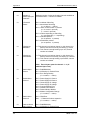
Record of Revisions
Revision
Level
Date
1
1.1
6-30-96
9-12-96
1.2
12-06-96
2.0
1-10-97
2.1
2.2
2.3
4-26-97
8-8-02
8-25-03
Reason for Change
Initial Release
Added cabling and interconnection drawing, added breakout panels
drawing, Added menu trees and configurable parameters.
Added DIP switch settings, added new J no’s to Fig. 2-1, minor
clarifications
Added Remote Communications specification, operator front panel
screens, enhanced operations section, added illustrations.
Major Revisions throughout
Revised and reformatted Technical Manual.
Revised Remote RLLP (Appendix A) Opcode 2202h.
Comments or Suggestions Concerning this Manual
Comments or suggestions regarding the content and design of this manual are appreciated. To
submit comments, please contact the Radyne ComStream, Inc. Customer Service Department.
vi
TM056 - Rev. 2.3
RCS20 M:N Redundancy Switch
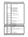
Table of Contents
Table of Contents
Section 1 – Introduction
1.0 Description _______________________________________________________ 1-1
1.1 Digital Data Switch (DDS20) _________________________________________ 1-1
1.2 Intermediate Frequency Switch (IFS20) ________________________________ 1-1
1.3 General Information ________________________________________________ 1-1
1.4 Channel Definitions ________________________________________________ 1-2
Section 2 – Installation
2.0 Installation Requirements____________________________________________ 2-1
2.1 Unpacking the System ______________________________________________ 2-1
2.1.1 List of Items_____________________________________________________ 2-1
2.1.2 In Case of Shipping Damage _______________________________________ 2-1
2.1.3 Test Data Sheet _________________________________________________ 2-1
2.2 Site Considerations ________________________________________________ 2-2
2.2.1 Power Sources __________________________________________________ 2-2
2.3 Rack Mounting ____________________________________________________ 2-2
2.4 System Cable Configuration _________________________________________ 2-3
2.5 System DIP Switch and Jumper Settings _______________________________ 2-5
2.5.1 Data Switch Module DIP Switch Configuration__________________________ 2-5
2.5.2 Reference Distribution Module ______________________________________ 2-9
2.6.1 J1 - SD - Send Data _____________________________________________ 2-11
2.6.2 J2 - DDO - Drop Data Out ________________________________________ 2-12
2.6.3 J3 - IDI - Insert Data In____________________________________________ 2-12
2.6.4 J4 - RD - Receive Data___________________________________________ 2-12
2.6.5 J5 - ESC Audio _________________________________________________ 2-12
2.6.6 J6 - ES/ES_____________________________________________________ 2-13
2.6.7 J7 – ESC Alarm Interface _________________________________________ 2-13
2.6.8 J8 - ESC 8K Data Interface________________________________________ 2-14
2.6.9 J9- G.703 (Balanced) ____________________________________________ 2-15
2.6.10 J10 - Sync Data________________________________________________ 2-15
2.6.11 Digital Data Switch (DDS20) J1 through J10 - Switch Connector _________ 2-16
2.6.12 RCU20 Connector Pinouts _______________________________________ 2-19
TM056 – Rev. 2.3
vii
Table of Contents
RCS20 M:N Redundancy Switch
Section 3 – Operation
3.0 Principles of Operation______________________________________________ 3-1
3.1 RCS20 Major Assemblies ___________________________________________ 3-1
3.1.1 Central Processing Unit (CPU) Board ________________________________ 3-1
3.2 Redundant Power Supplies __________________________________________ 3-1
3.3 RCU20 Rear Panel ________________________________________________ 3-1
3.4 IFS20 Major Assemblies ____________________________________________ 3-2
3.5 IF Switch Relays __________________________________________________ 3-2
3.6 DDS20 Major Assemblies ___________________________________________ 3-2
Section 4 – User Interfaces
4.0 Operating Procedures ______________________________________________ 4-1
4.1 Front Panel Control ________________________________________________ 4-1
4.1.1 Front Panel Layout and Features ____________________________________ 4-1
4.1.2 Front Panel LCD Display __________________________________________ 4-1
4.1.3 Front Panel Keypad_______________________________________________ 4-2
4.1.3.1 MODEM-MOD CONFIG __________________________________________ 4-3
4.1.3.2 MODEM-DEMOD CONFIG _______________________________________ 4-3
4.1.3.3 MODEM-INTFC CONFIG _________________________________________ 4-3
4.1.3.4 MODEM-MONITOR _____________________________________________ 4-3
4.1.3.5 MODEM-TEST _________________________________________________ 4-3
4.1.3.6 MODEM-ALARMS ______________________________________________ 4-3
4.1.3.7 SWITCH-CONFIG SWITCH ______________________________________ 4-3
4.1.3.8 SWITCH-CONFIG SYSTEM ______________________________________ 4-3
4.1.3.9 SWITCH-MONITOR/ALARMS _____________________________________ 4-4
4.1.3.10 SWITCH-TEST _______________________________________________ 4-4
4.1.4 Front Panel LCD Indicators_________________________________________ 4-4
4.1.5 Guide to Front Panel Monitor and Control______________________________ 4-4
4.2 Remote Port Control _______________________________________________ 4-5
4.3 Terminal Port Control_______________________________________________ 4-5
4.3.1 Terminal Interface ________________________________________________ 4-5
4.4 Modem Checkout and Initial Power-up _________________________________ 4-5
4.5 RCS20 Front Panel Data Entry Screens ________________________________ 4-6
viii
TM056 - Rev. 2.3
RCS20 M:N Redundancy Switch
Table of Contents
4.5.1 Basic Front Panel Controls _________________________________________ 4-6
4.5.1.1 Changing parameters from the Front Panel __________________________ 4-7
4.5.1.2 Moving to the Next Screen in a Menu Tree ___________________________ 4-7
4.5.1.3 Moving to the Previous Screen in a Menu Tree ________________________ 4-7
4.5.1.4 Summary of Basic Front Panel Controls _____________________________ 4-8
4.6 Front Panel Menu Trees and Screens __________________________________ 4-8
4.7 Host Computer Remote Communications _____________________________ 4-12
4.7.1 Protocol Structure _______________________________________________ 4-12
4.7.2 Protocol Wrapper _______________________________________________ 4-12
4.7.3 Frame Description and Bus Handshaking ____________________________ 4-14
4.7.4 Global Response Operational Codes ________________________________ 4-14
4.7.5 Collision Avoidance______________________________________________ 4-15
4.7.6 Software Compatibility ___________________________________________ 4-16
4.7.7 RLLP Summary ________________________________________________ 4-17
4.7.8 RCS20 Opcode Command Set ____________________________________ 4-18
4.7.9 RCS20 Channel Definitions _______________________________________ 4-19
4.7.10 Detailed Command Descriptions __________________________________ 4-19
4.8 Ethernet Port User Interface ________________________________________ 4-19
4.9 RCS20 Management Information Base (MIB) ___________________________ 4-19
4.10 Terminal Port User Interface _______________________________________ 4-19
Section 5 – Electrical Interfaces
5.0 RCS20 Connections _______________________________________________ 5-1
5.1 DIP Switch Settings ________________________________________________ 5-7
5.2 DDS20 Connector Pinouts __________________________________________ 5-9
5.2.1 J1 - SD - Send Data ______________________________________________ 5-9
5.2.2 J2 - DDO - Drop Data Out _________________________________________ 5-9
5.2.3 J3 - IDI - Insert Data In_____________________________________________ 5-9
5.2.4 J4 - RD - Receive Data____________________________________________ 5-9
5.2.5 J5 - ESC Audio __________________________________________________ 5-9
5.2.6 J6 - ES/ES_____________________________________________________ 5-10
TM056 – Rev. 2.3
ix
Table of Contents
RCS20 M:N Redundancy Switch
Section 6 – Maintenance
6.0 Periodic Maintenance and Troubleshooting______________________________ 6-1
6.1 Troubleshooting ___________________________________________________ 6-1
6.1.1 Checking the Cabling and Connectors ________________________________ 6-1
6.1.2 Checking the Fuses ______________________________________________ 6-1
6.2 RCS20 Alarms ____________________________________________________ 6-2
6.2.1 Major Alarms ____________________________________________________ 6-2
6.2.2 Minor Alarms ____________________________________________________ 6-3
6.2.3 Alarm Masks ____________________________________________________ 6-4
6.2.4 Latched Alarms __________________________________________________ 6-4
6.3 Equipment Return and Repair Procedure _______________________________ 6-4
Section 7 – Technical Specifications
7.0 Introduction_______________________________________________________ 7-1
7.1 General Specifications ______________________________________________ 7-1
7.2 Monitor and Control ________________________________________________ 7-1
7.4 Power and Environmental ___________________________________________ 7-2
7.5 Physical _________________________________________________________ 7-2
Appendix A – Remote RLLP
A.1 Detailed Command Descriptions _____________________________________ A-1
Appendix B – SNMP MIB
Glossary
x
TM056 - Rev. 2.3
RCS20 M:N Redundancy Switch
Introduction
Section 1 – Introduction
1.0 Description
The Radyne ComStream, Inc. RCS20 M:N Redundancy Switch provides backup
switching/protection for up to nine pairs of satellite modem channels (modulators/demodulators).
The RCS20 is a companion product to the Radyne DMD15/2400 family of Satellite Modems.
The RCS20 is comprised of three separate units that make up the switching system; the
Redundancy Control Unit (RCU20), the Digital Data Switch (DDS20) and the Intermediate
Frequency Switch (IFS20).
The RCS20 can be operated automatically, in which case an automatic backup of a failed online
modem occurs after a preprogrammed delay. The switch may also be operated manually, allowing
the operator to manually switch to a backup modem. Front panel controls and indicators provide for
auto/manual configuration, as well as display of online/off line status information for all modems in
the redundancy configuration.
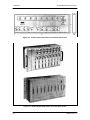
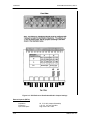
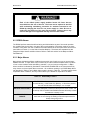
Figure 1. RCS20 M:N Redundancy Switch
1.1 Digital Data Switch (DDS20)
The DDS20 provides all of the data interconnections between the online and backup modems. The
DDS20 also provides buffering of terrestrial data signals to backup modulators allowing ‘hot-standby’
modes of operation. The DDS20 receives control and DC power through an interconnecting cable
from the RCU20.
1.2 Intermediate Frequency Switch (IFS20)
The IFS20 Intermediate Frequency Switch interfaces the IF signals of the modems with the Earth
Station IF system and provides backup switching. The unit provides all of the switching relays,
signal splitters and terminations that are necessary to connect any combination of up to nine
Modulators and Demodulators to nine independent uplink and nine independent downlink
transponders. The IFS20 receives control and DC power through an interconnecting cable from the
RCU20.
1.3 General Information
Every attempt has been made to include all of the information that is necessary to properly operate
the RCS20. However, although basic information is included on theory of operation and
TM056 – Rev. 2.3
1-1
Introduction
RCS20 M:N Redundancy Switch
troubleshooting, this is not a service or maintenance manual. Also, the user should be fully familiar
with the operation of the individual Satellite Modems, Modulators and/or Demodulators that will be
connected to the Switch. Throughout this manual any reference to the RCS20 indicates the
combination of the RCU20, IFS20 and the DDS20. Refer to Figure 1-1 for a pictorial representation
of the RCU20 front panel, Figure 1-2 for a Functional Block Diagram of the RCS20 System and
Figure 2-7 for an interconnection diagram of the complete system including the cabling
requirements.
1.4 Channel Definitions
The RCS20 organizes the modems connected to the switch according to satellite communications
channels. These channels are labeled on the DDS20 and IFS20 panels, and are defined as follows:
Channel 0
Channel 1
Channel 2
Channel 3
Channel 4
Channel 5
Channel 6
Channel 7
Channel 8
Channel 9
1-2
- Backup 1
- Modem 1
- Modem 2
- Modem 3
- Modem 4
- Modem 5
- Modem 6
- Modem 7
- Modem 8
- Modem 9/Backup 2
TM056 - Rev. 2.3
RCS20 M:N Redundancy Switch
Installation
Section 2 – Installation
2.0 Installation Requirements
This chapter instructs the user in the methods for setting up and installing an RCS20 M:N
Redundancy Switch into a Satellite Modem system. The cabling configurations for up to nine
channels and nine transponders are described.
2.1 Unpacking the System
Unseal the shipping cartons taking care not to damage the cartons, the packing material or the
equipment inside. The cartons and the packing material should be saved in the event that an
RCS20 will need to be reshipped. Examine the exterior of the units for any possible shipping
damage.
2.1.1 List of Items
Carefully remove the units from the cartons. In addition to this manual, verify that the following
items are present:
•
•
•
•
•
•
•
•
•
RCS20 Redundancy Control Unit
IFS20 or IFS20A Intermediate Frequency Switch
2 ea. AC Power Cords
2 ea. Bank Control 15-pin HD Sub Cables
M:N Switch System Test Data Sheet
M:N Switch to Modem Cable(s) for Backup Modulator and Demodulator
Test I/O Mating Connector
Optional 1:N Switch to Modem, I/O and Coaxial Cables for Modems 1 – 9
Optional Modem bypass cable(s) for Modems 1 – 9
2.1.2 In Case of Shipping Damage
If any shipping damage is discovered to any of the above listed equipment, promptly contact the
transporter and file a damage claim. The transporter is responsible for any damage caused during
shipping. Radyne, Inc. should also be contacted.
Damage as a result of transport is not covered under the Radyne, Inc. Warranty. Refer to the
Warranty section in the front of this manual for further information.
The procedure for returning faulty or damaged equipment is contained in the warranty section in the
front of this manual.
2.1.3 Test Data Sheet
Each RCS20 M:N Redundancy Switch system is shipped with a Test Data Sheet. This report
contains information on the results of the Switch quality control testing. The report also includes
information pertaining to the system settings that were made at the factory. Radyne, Inc.
recommends that the user save this report for future reference.
TM056 - Rev. 2.3
2-1
Installation
RCS20 M:N Redundancy Switch
2.2 Site Considerations
Adequate site planning and preparation simplifies the installation process and results in a more
reliable system. The user should ensure that the site has adequate electrical power, environmental
controls and protection against sources of electrical radiation and interference.
2.2.1 Power Sources
The power sources should be properly grounded and as free as possible from electrical interference.
If a redundant configuration is to be used, then each power cord on the RCS20 must be plugged into
its own separate power circuit. Each circuit must have its own independent circuit breaker.
Grounding is achieved automatically when the three-prong power plug is inserted into a power
receptacle. Verify by testing that there is no voltage present between the chassis of the Switch and
the power line ground.
The protective ground must not be bypassed with a three prong to
two-prong adapter or defeated in any way. Defeating the ground may
result in operator injury or damage to the system.
2.3 Rack Mounting
The RCS20 is designed so that it can be mounted in a standard 19-inch rack. The RCS20 is 5¼”, 3
Rack Units (RU) high and must be mounted on the front of a rack with the front panel facing forward
as shown in Figure 1-1.
The DDS20 is 8¾” (5 RU) high and is preferably mounted at the top of a rack unit with the Terrestrial
Interface connectors available at the top of the rack and the modem connections available at the at
the bottom of the DDU20 in the interior of the rack. The DDS20 may also be mounted at the rear of
a rack with the Terrestrial Interface connectors available at the rear of the rack and the modem
connections available in the interior of the rack.
The IFS20A is also 8¾” (5 RU) high and is designed to be mounted at the rear of a rack with the
Up/Downconverter interface connections facing to the rear of the rack with the modem IF
connections available in the interior of the rack. The IFS20A may also be mounted in the top of a
rack with the Up/Downconverter interface connections available at the top of the rack and the
modem IF connections available inside the rack.
To allow for the easy installation of cables and adequate air circulation through the units, a
minimum of six of clearance must be provided at the sides and rear of the units. In addition, the
RCS20 requires a minimum of 1¾” (1 RU) of clearance on top of the unit.
If the Switch is mounted on slide mounts, the cables must be of sufficient length to allow the units
to be pulled forward on the mounts.
2-2
TM056 - Rev. 2.3
RCS20 M:N Redundancy Switch
Installation
2.4 System Cable Configuration
This section describes the cabling configurations for the various combinations of DMD15/2400
Modulators/Demodulators/Modems and Transponders. The following figures are provided to
illustrate the proper placement of the cables:
Figure 2-1. RCU20 Rear Panel
Figure 2-2. IFS20 Rear Panel
TM056 - Rev. 2.3
2-3
Installation
RCS20 M:N Redundancy Switch
Figure 2-3. IFS20 Chassis Base Unit Rear Available Connectors
Figure 2-4. DDS20 Digital Data Switch Front and Rear Panels
2-4
TM056 - Rev. 2.3
RCS20 M:N Redundancy Switch
Installation
Figure 2-5. DDS20 Rear Panel Interface – Data Switch Module
If either AC line cord remains connected to the RCS20, dangerous AC
voltages will be present within the Switch and the cooling fan will also be
operational. The top cover of the Switch should not be removed unless
one of the power supplies is to be replaced following the Instructions in
Section 4.
Although AC power is not present on the back plane, care must be taken
when Installing or removing a plug-in module since DC voltages will be
present.
The IFS20 and DDS20 receive DC power through the RCS20 interconnection
cable. Therefore, to ensure that no DC power is being applied to the back
plane modules, both of the Switch's AC line cords or the RCS20
interconnection cable must be removed.
2.5 System DIP Switch and Jumper Settings
The RCS20 requires several DIP Switches and jumpers to be configured for proper operation. The
DIP Switches are located on the Digital Data Switches (DDS20) and the jumpers are located on the
optional Reference Distribution Module on the RCU20 (See Figure 2-8).
2.5.1 Data Switch Module DIP Switch Configuration
Two Part Numbers exist for Data Switch Modules on the DDS20; AS/3356 (Figure 2-6a) and
AS/3478 (Figure 2-6b and 2-6c for AS/3478 Rev. A2 forward only).
TM056 - Rev. 2.3
2-5
Installation
RCS20 M:N Redundancy Switch
The AS/3356 Modules were shipped with older models of the DDS20. Refer to Tables 2-1 through
2-5 for the various DIP Switch configurations on these assemblies.
Figure 2-6a. AS/3356 Data Switch Module
2-6
TM056 - Rev. 2.3
RCS20 M:N Redundancy Switch
Installation
Figure 2-6b. AS/3356 Data Switch Module
TM056 - Rev. 2.3
2-7
Installation
RCS20 M:N Redundancy Switch
Figure 2-6c. AS/3356 Data Switch Module (for AS/3478 Rev. A2 Forward Only)
2-8
TM056 - Rev. 2.3
RCS20 M:N Redundancy Switch
Installation
Figure 2-7. Complete System Interconnection and Cabling Information for System
Configuration
2.5.2 Reference Distribution Module
The Reference Distribution Module (RDM) is an optional RCU20 expansion card that is used to
buffer and distribute earth station frequency reference(s) to the external reference input of modems
that are connected to an RCS20. The RDM automatically switches between EXT A, EXT B or Internal
References based upon onboard Clock Activity Detect circuits.
The RDM is illustrated in Figure 2-8. There are six BNC-type connectors on the RDM. The function
of the individual connectors is as follows:
J1
J2
J3
J4
J5
J6
EXTA IN
EXTB IN
OUT 1
OUT 2
OUT 3
OUT 4
Primary Internal Reference Input
Secondary Internal Reference Input
Reference Output 1
Reference Output 2
Reference Output 3
Reference Output 4
The RDM also contains an internal reference in two options; High-stability or normal. These options
and the electrical specifications for the above connectors are shown below.
TM056 - Rev. 2.3
2-9
Installation
RCS20 M:N Redundancy Switch
Figure 2-8. RCU Reference Distribution Module Jumper Settings
External Input A (EXT A)
Impedance:
Frequency:
Input Level Spec.:
2-10
50, 75, 510O (Jumper-Selectable)
1.25, 2.5, 5.0 and 10.0 MHz
High Level 2 to 5 Volts
TM056 - Rev. 2.3
RCS20 M:N Redundancy Switch
Installation
Low Level 0 to 0.8 Volts
External Input B (EXT B)
Impedance:
Frequency:
Input Level Spec.:
50, 75, 510O (Jumper-Selectable)
1.25, 2.5, 5.0 and 10.0 MHz
High Level 2 to 5 Volts
Low Level 0 to 0.8 Volts
Internal Reference (Option 1)
Stability:
Output Frequency:
1 x 10⁻⁵
1.25, 2.5, 5.0 and 10.0 MHz (Program-selectable to
match External Input)
Internal Reference (Option 2)
Stability:
Aging (day):
Aging (year):
Output Frequency:
1 x 10⁻⁸
1 x 10⁻⁸
1 x 10⁻⁸
1.25, 2.5, 5.0 and 10.0 MHz (Program-selectable to
match External Input)
Microprocessor Interface
External 1/ External 2/ Internal Reference Select
External Input Activity Detectors
Internal Reference Activity Detector
Reference Output (OUT1, OUT2, OUT3, OUT4)
Output Level:
Output Current Drive:
Output Frequency:
Output Impedance:
Short Circuit Resistant
TTL
48 mA Maximum
Sufficient to drive 5:
DMD15
DVB3000
DMD2401
Sufficient to drive 3: DMD2400
Same as External Input
50O
Board Outline
RCS20 Option Card Slot/DIN Connector
2.6 DDS20 Connector Pinouts
The following connectors are located on the Universal Interface Module on the DDS20. Refer to the
following Tables for the connector pinouts.
2.6.1 J1 - SD - Send Data
J1 is the G.703 Unbalanced Send Data (SD) BNC connector located on the Universal Interface
Module.
TM056 - Rev. 2.3
2-11
Installation
RCS20 M:N Redundancy Switch
2.6.2 J2 - DDO - Drop Data Out
J2 is the Unbalanced Drop Data Out (DDO) BNC connector located on the Universal Interface
Module.
2.6.3 J3 - IDI - Insert Data In
J3 is the Unbalanced Insert Data In (IDI) BNC connector located on the Universal Interface Module.
2.6.4 J4 - RD - Receive Data
J4 is the Unbalanced Receive Data (RD) BNC connector located on the Universal Interface Module.
2.6.5 J5 - ESC Audio
J5 is the 9-pin ‘D’ Female ESC Audio Channel connector. The pinouts for this connector
shown below in Table 2-6.
are
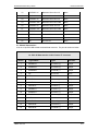
Table 2-6. J5 - ESC Audio - 9-Pin ‘D’ Female
2-12
Pin No.
Signal
Description
Direction
1
ESCAUD TX 1A
Tx Audio 1A (-)
Input
2
ESCAUDRX 1A
Rx Audio 1A (-)
Output
3
GND
Ground
None
4
ESCAUDTX 2B
Tx Audio 2B (+)
Input
5
ESCAUDRX 2A
Rx Audio 2A (-)
Output
6
ESCAUDTX 1B
Tx Audio 1B (+)
Input
7
ESCAUDRX 1B
Rx Audio 1B (+)
Output
8
ESCAUDTX 2A
Tx Audio 2A (-)
Input
9
ESCAUDRX 2A
Rx Audio 2A (-)
Output
TM056 - Rev. 2.3
RCS20 M:N Redundancy Switch
Installation
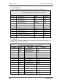
2.6.6 J6 - ES/ES
The connector pinouts for J6, the 9-Pin Earth-Station-to-Earth-Station asynchronous data connector
are shown below.
Table 2-7. J6 - ES/ES - 9-Pin ‘D’ Female
Pin No.
Signal
Description
Direction
1
GND
Ground
None
2
RXD-232
Receive Data RS232
Output
3
TXD-232
Transmit Data RS232
Input
4
TXD-B
Transmit Data RS485 (+)
Input
5
TXD-A
Transmit Data RS485 (-)
Input
6
NC
No Connection
None
7
NC
No Connection
None
8
RXD-B
Receive Data B RS485 (+)
Output
9
RXD-A
Receive Data A RS485 (-)
Output
2.6.7 J7 – ESC Alarm Interface
The connector pinouts for J7, the 25-Pin ESC Alarm Interface are shown below.
Table 2–8. J7 - ESC Alarm Interface - 25-Pin Female ‘D’
Pin Number
Signal
Description
Direction
1
GND
Ground
None
2
ESCBWO 1 NO
Backward Alarm Out-1 NO
None
3
NC
No Connection
None
4
ESCBWO 1 NO
Backward Alarm Out-2 NO
None
5
NC
No Connection
None
6
ESCBWO 4 NO
Backward Alarm Out-4 NO
None
7
GND
Ground
None
8
ESCBWO 4 NO
Backward Alarm Out-4 NO
None
9
NC
No Connect
None
10
ESCBWI 2
Backward Alarm In 2
Input
11
ESCBWI 4
Backward Alarm In 4
Input
12
NC
No Connect
None
13
NC
No Connect
None
TM056 - Rev. 2.3
2-13
Installation
RCS20 M:N Redundancy Switch
14
ESCBWO 1C
Backward Alarm Out 1-C
None
15
ESCBWO 1-NC
Backward Alarm Out 1-NC
None
16
ESCBWO 2-C
Backward Alarm Out 2-C
None
17
ESCBWO 2-NC
Backward Alarm Out 2-NC
None
18
ESCBWO 3-C
Backward Alarm Out 3-C
None
19
ESCBWO 3-NC
Backward Alarm Out 3-NC
None
20
ESCBWO 4-C
Backward Alarm Out 4-C
None
21
ESCBWO 4-NC
Backward Alarm Out 4-NC
None
22
ESCBWI 1
Backward Alarm In 1
Input
23
ESCBWI 1
Backward Alarm In 3
Input
24
NC
No Connection
None
25
NC
No Connect
None
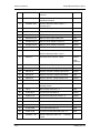
2.6.8 J8 - ESC 8K Data Interface
J8 is the 15-pin ESC IDR 8-Kbit overhead data connector. The pinouts are shown below.
Table 2-9. J8 - ESC 8K Data Interface 15-Pin Female ‘D’ Connector
2-14
Pin No.
Signal Name
Signal
Direction
1
ESCRXO-B
Rx Octet-B (+)
Output
2
ESCRXC-B
Rx Clock-B (+)
Output
3
ESCRXD-B
Rx Data-B (+)
Output
4
NC
No Connect
None
5
NC
No Connect
None
6
ESCTXD-A
Tx Data-A (-)
Output
7
ESCTXC-A
Tx Clock-A (-)
Output
8
ESCTXO-A
Tx Octet-A (-)
Output
9
ESCRXO -A
Rx Octet-A (-)
Output
10
ESCRXC-A
Rx Clock-A (-)
Output
11
ESCRXD-A
Rx Data-A (-)
Output
12
GND
Ground
None
13
ESCTXD-B
Tx Data-B (+)
Input
14
ESCTXC-B
Tx Clock-B (+)
Output
15
ESCTXO-B
Tx Octet-B (+)
Output
TM056 - Rev. 2.3
RCS20 M:N Redundancy Switch
Installation
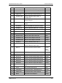
2.6.9 J9- G.703 (Balanced)
J9 is the G.703 (Balanced) 15-pin data connector. The pinouts are shown below.
Table 2-10. J9 - G.703 (Balanced) 15-Pin Female ‘D’ Connector
Pin No.
Signal Name
Signal
Direction
1
Send Data A (-)
SD-A
Input
9
Send Data B (+)
SD-B
Input
7
External Clock A (-)
BAL EXC-A
Input
8
External Clock B (+)
BAL EXC-B
Input
3
Receive Data A (-)
RD-A
Output
11
Receive Data B (+)
RD-B
Output
12
Drop Data Out A (-)
DDO-A
Output
5
Drop Data Out B (+)
DDO-B
Output
13
Insert Data In A (-)/EXC A (-)
IDI-A
Input
6
Insert Data In B (+)/ESC B (+)
IDI-B
Input
2.6.10 J10 - Sync Data
J10 is the 37-pin synchronous data connector located on the Universal Interface Module. The
pinouts are shown below in Table 2-11.
Table 2–11. J10 - Sync Data RS422/RS485/V.35 - 37-Pin Female
Pin Number
Signal
Description
Direction
3
TXO-A
Transmit Octet A (-)
Input
21
TXO-B
Transmit Octet B (+)
Input
4
SD-A
Send Data A (-)
Input
22
SD-B
Send Data B (+)
Input
5
ST-A
Send Timing A (-)
Output
23
ST-B
Send Timing B (+)
Output
6
RD-A
Receive Data A (-)
Output
24
RD-B
Receive Data B (+)
Output
7
RS-A
Request to Send A (-)
Input
25
RS-B
Request to Send B (+)
Input
8
RT-A
Receive Timing A (-)
Output
26
RT-B
Receive Timing B (+)
Output
TM056 - Rev. 2.3
2-15
Installation
RCS20 M:N Redundancy Switch
9
CS-A
Clear to Send A (-)
Output
10
MF
Mod Fault - Open
Collector
Output
28
DF
Demod Fault - Open
Collector
Output
27
CS-B
Clear to Send B (+)
Output
11
DM-A
Data Mode A (-)
Output
29
DM-B
Data Mode B (+)
Output
13
RR-A
Receiver Ready A (-)
Output
31
RR-B
Receiver Ready B (+)
Output
15
BAL EXC-A
External Clock A (-)
Input
33
BAL EXC-B
External Clock B (+)
Input
16
RX-0-A
Receive Octet A (-)
Output
34
RX-0 B
Receive Octet B (+)
Output
17
TT-A
Terminal Timing A (-)
Input
35
TT-B
Terminal Timing B (+)
Input
1, 19, 20, 37
GND
Signal Ground
2.6.11 Digital Data Switch (DDS20) J1 through J10 - Switch Connector
J1 through J10 are the 68-Pin high-density data connectors that carry data to and from the modem.
The pinouts for these connectors are shown below in Table 2-12.
Table 2-12. J18 - Switch Connector - 68-Pin High-Density Female
2-16
Pin No.
Signal
Description
Direction
1
G.703B SD-A
G.703 Send Data Input A (-)
Input
2
SYNC SD-A
Synchronous Data Send Data Input -A (-)
Input
3
ESCBWO 1C
IDR ESC Backward Alarm Out - 1 Common
None
4
G.703B IDI-A
G.703 Insert Data Input - A (-)
Input
5
SYNC ST-A
Synchronous Data Send Timing Output - A
Output
6
ESCBWO 1NO
IDR ESC Backward Alarm Out - 1 Normally
Open
Input
7
SYNC TT-A
Synchronous Data Terminal Timing Input A
Input
8
ESCBWO 2NC
IDR ESC Backward Alarm Out - 2 Normally
Closed
9
DDO-A RT-A
G.703 Drop Data Out A - Synchronous Data
Receive Timing Output - A
Output
TM056 - Rev. 2.3
RCS20 M:N Redundancy Switch
Installation
10
ESCBWO 3C
IDR ESC Backward Alarm Output - 3
Common
11
IDO-A RD-A
G.703 Insert Data Out A - Synchronous
Data Receive Data A
12
ESCBWO 3NO
IDR ESC Backward Alarm Output - 3
Normally Open
13
BAL EXC-A
External Clock Input - A
14
GND
Ground
15
ESCAUDTX 1A
IDR ESC Audio Input Channel 1A
Input
16
ESCAUDTX 2A
IDR ESC Audio Input Channel 2A
Input
17
ESCAUD RX 1A
IDR ESC Audio Output Channel 1A
Output
18
ESCAUD RX 2A
IDR ESC Audio Output Channel 2A
Output
19
ESCBWI 3
IDR ESC Backward Alarm Input - 3
Input
20
TXD-A BWI 1
IBS ES Transmit Data A
Input
Output
Input
IDR ESC Backward Alarm Input 1
21
MOD FLT
Mod Fault Open Collector Output
Output
Open
Collector
22
ES RXD-A
IBS ES Receive Data Output - A
Output
23
ES DSR
IBS ES Data Set Ready (RS232 Only)
Output
24
ESCTXC-A
IDR ESC Transmit 8 Kbps Output Clock
Output
25
ESCTXD-A
IDR ESC Transmit 8 Kbps Output Data
Input
26
ESCRXC-A
IDR ESC Receive 8 Kbps Output Clock
Output
27
ESCRXD-A
IDR ESC Receive 8 Kbps Output Data
Output
28
ESCBWO 4NC
IDR ESC Backward Alarm Output - 4
Normally Closed
29
TXO-A
IBS Transmit Octet Input - A
Input
30
SYNC DM-A
Synchronous Data Mode A
Output
31
SYNC CS-A
Synchronous Data Clear to Send - A
Output
32
RXO-A
IBS Receive Octet Output - A
Output
33
SYNC RS-A
Synchronous Data Request to Send A
Input
34
SYNC RR-A
Synchronous Data Receiver Ready - A
Output
35
G703B SD-B
G.703 Send Data Input - B
Input
36
SYNC SD-B
Synchronous Data Send Data Input - B
Input
37
ESCBWO 1 NC
IDR ESC Backward Alarm Out - 1 Normally
Closed
TM056 - Rev. 2.3
2-17
Installation
RCS20 M:N Redundancy Switch
38
G703B IDI-B
G.703 Insert Data Input - B
39
SYNC ST-B
Synchronous Data Send Timing Output B
40
ESCBWO 2C
IDR ESC Backward Alarm Out 2 Common
41
SYNC TT-B
Synchronous Data Terminal Timing - B
42
ESCBWO 2NO
IDR ESC Backward Alarm Output 2
Normally Open
43
DDO-B RT-B
G.703 Drop Data Out - B Synchronous Data
Receive Timing B
44
ESCBWO 3NC
IDR ESC Backward Alarm Out - 3 Normally
Closed
45
IDO-B RD-B
G.703 Insert Data Out Synchronous Data
46
ESCBWO 4C
IDR ESC Backward Alarm Out - 4 Common
47
BAL EXC-B
External Clock Input B
48
GND
Ground
49
ESCAUDTX 1B
IDR ESC Audio Input Channel 1B
Input
50
ESCAUDTX 2B
IDR ESC Audio Input Channel 2B
Input
51
ESCAUDRX 1B
IDR ESC Audio Output Channel 1B
Output
52
ESCAUDRX 2B
IDR ESC Audio Output Channel 2B
Output
53
ESCBWI 4
IDR ESC Backward Alarm Input - 4
54
TX-B BWI 2
IBS ES Transmit Data B
Input
Input
IDR ESC Backward Alarm Input 2
55
DMD FLT
Demod Fault Open Collector Output
Output
Open
Collector
2-18
56
ES RXD-B
IBS ES Receive Data Input - B
Output
57
GND
Ground
58
ESCTXC-B
IDR ESC Transmit 8 Kbps Output Clock B
Output
59
ESCTXD-B
IDR ESC Transmit 8 Kbps Output Data B
Input
60
ESCRXC-B
IDR ESC Receive 8 Kbps Clock Output B
Output
61
ESCRXD-B
IDR ESC Receive 8 Kbps Data Output B
Output
62
ESCBWO 4NO
IDR ESC Backward Alarm Out - 4 Normally
Open
63
TXO-B
IBS Transmit Octet Input B
Input
64
SYNC DM-B
Synchronous Data - Data Mode Out B
Output
65
SYNC CS-B
Synchronous Data - Clear to Send B
Input
66
RXO-B
IBS Receive Octet Output B
Output
TM056 - Rev. 2.3
RCS20 M:N Redundancy Switch
Installation
67
SYNC RS-B
Synchronous Data Request to Send - B
Input
68
SYNC RR-B
Synchronous Data Receiver Ready B
Output
2.6.12 RCU20 Connector Pinouts
Table 2-13. J1 - Switch Interface Control Card - Alarms - 9-pin ‘D’ Male
Pin No.
Signal
Description
Direction
1
MJA-NC
Major Alarm - NC
None
2
MJA-C
Major Alarm - C
None
3
MJA-NO
Major Alarm - NO
None
4
NC
No Connect
None
5
NC
No Connect
None
6
NC
No Connect
None
7
MNA-NC
Minor Alarm - NC
None
8
MNA-C
Minor Alarm - C
None
9
MNA-NO
Minor Alarm - NO
None
Table 2-14. J2 - Switch Interface Control Card - RS232 Terminal Interface - 9-Pin
‘D’ Female
Pin No.
Signal
Description
Direction
1
NC
No Connect
None
2
RxD
Receive Data
Input
3
TxD
Transmit Data
Output
4
NC
No Connect
None
5
GND
Ground
None
6
NC
No Connect
None
7
NC
No Connect
None
8
NC
No Connect
None
9
NC
No Connect
None
TM056 - Rev. 2.3
2-19
Installation
RCS20 M:N Redundancy Switch
Table 2-15. J3 - Switch Interface Control Card - RS485 Remote Interface - 9-Pin
‘D’ Female
Pin No.
Signal
Description
Direction
1
TxD-B
Transmit Data B (+)
Output
2
NC
No Connect
None
3
NC
No Connect
None
4
NC
No Connect
None
5
COMMON
Signal Common
None
6
TxD-A
Transmit Data A (-)
Output
7
NC
No Connect
None
8
RxD-B
Receive Data B (+)
Input
9
RxD-A
Receive Data A (-)
Input
Table 2-16. J3 - Switch Interface Control Card - RS232 Terminal Interface - 9-Pin
‘D’ Female
2-20
Pin No.
Signal
Description
Direction
1
NC
No Connect
None
2
RxD
Receive Data
Input
3
TxD
Transmit Data
Output
4
NC
No Connect
None
5
GND
Ground
None
6
NC
No Connect
None
7
NC
No Connect
None
8
NC
No Connect
None
9
NC
No Connect
None
TM056 - Rev. 2.3
RCS20 M:N Redundancy Switch
Installation
Table 2-17. J3 - Bank Control Card - DDS20 Control and Power - 15-pin HD
‘D’ Female
Pin No.
Signal
Description
Direction
1
DDS_LCLK
Serial Control Clock
Output
2
VCC_RELAY
Relay +6 Volts
Output
3
DDS_LDAT2
Serial Control Data 2
Bi-directional
4
GND
Ground
None
5
GND
Ground
None
6
VCC
Logic +5 Volts
Output
7
VCC_RELAY
Relay +6 Volts
Output
8
VCC_RELAY
Relay +6 Volts
Output
9
GND
Ground
None
10
GND
Ground
None
11
VCC_RELAY
Relay +6 Volts
Output
12
DDS_LDAT1
Serial Control Data 1
Bi-directional
13
GND
Ground
None
14
DDS_LDAT3
Serial Control Data 3
Bi-directional
15
INT
DDS20 Interrupt
Input
Table 2-18. J2 - Bank Control Card - IFS20 Control and Power - 15-pin HD
‘D’ Female
Pin No.
Signal
Description
Direction
1
IFS_LCLK
Serial Control Clock
Output
2
NC
No Connect
None
3
NC
No Connect
None
4
GND
Ground
None
5
GND
Ground
None
6
VCC
Logic +5 Volts
Output
7
VCC_RELAY
Relay +6 Volts
Output
8
NC
No Connect
None
9
NC
No Connect
None
10
GND
Ground
None
11
VCC_RELAY
Relay +6 Volts
Output
TM056 - Rev. 2.3
2-21
Installation
RCS20 M:N Redundancy Switch
12
IFS_LDAT1
Serial Control Data 1
Bi-directional
13
NC
No Connect
None
14
NC
No Connect
None
15
NC
No Connect
None
Table 2-19. J1 - Bank Control Card - RS485 Modem Control - 9-pin ‘D’ Female
2-22
Pin No.
Signal
Description
Direction
1
TxD-B
RS485/HDLC Transmit Data B (+)
Output
2
TCLK-A
HDLC Transmit Clock A (-)
Output
3
TCLK-B
HDLC Transmit Clock B (+)
Output
4
RCLK-A
HDLC Receive Clock A (-)
Input
5
COMMON
Signal Common
None
6
TxD-A
RS485/HDLC Transmit Data A (-)
Output
7
RCLK-B
HDLC Receive Clock B (+)
Input
8
RxD-B
RS485/HDLC Receive Data B (+)
Input
9
RxD-A
RS485/HDLC Receive Data A (-)
Input
TM056 - Rev. 2.3
RCS20 M:N Redundancy Switch
Installation
Table 2-20. IFS20, J42 - IFS20 Control and Power - 15-pin HD ‘D’ Female
Pin No.
Signal
Description
Direction
1
IFS_LCLK
Serial Control Clock
Input
2
NC
No Connect
None
3
NC
No Connect
None
4
GND
Ground
None
5
GND
Ground
None
6
VCC
Logic +5 Volts
Input
7
VCC_RELAY
Relay +6 Volts
Input
8
NC
No Connect
None
9
NC
No Connect
None
10
GND
Ground
None
11
VCC_RELAY
Relay +6 Volts
Output
12
IFS_LDAT1
Serial Control Data 1
Bi-directional
13
NC
No Connect
None
14
NC
No Connect
None
15
NC
No Connect
None
TM056 - Rev. 2.3
2-23
Installation
2-24
RCS20 M:N Redundancy Switch
TM056 - Rev. 2.3
RCS20 M:N Redundancy Switch
Operation
Section 3 – Operation
3.0 Principles of Operation
This chapter provides additional basic information on the RCU20 and IFS20 hardware and internal
operation.
3.1 RCS20 Major Assemblies
The RCU20 Redundancy Control Unit contains the modules that control and monitor the operation of
the M:N Switch System. The RCU20 is composed of the following major assemblies and
components:
1.
2.
3.
4.
5.
6.
7.
Central Processor Unit (CPU) Board
Front Panel Board
Controller Interface Module
Clock Distribution Module (optional)
Dual Redundant Power Supplies
Ethernet Module (optional)
Bank Control Module
3.1.1 Central Processing Unit (CPU) Board
The Central Processor Unit (CPU) Board contains the M:N Switch intelligence and memory
circuitry. The on-board microprocessor is an MC68302, which has a 24-bit address bus and a 16bit data bus. The microprocessor controls and coordinates all major functions of the Switch and
performs all necessary calculations. The non-volatile system memory on the board stores the
switching parameter settings for each Modem Channel. Control and data signals are routed to the
appropriate devices in the system through various latches and transceivers that are controlled by
the microprocessor.
3.2 Redundant Power Supplies
The M:N Switch comes equipped with two fully redundant internal power supplies (PS1 and PS2)
that supply DC voltage to the system. Each supply is fully independent of the other, including their
source of AC power and fusing.
The Switch can remain fully operational as long as it is supplied with a source of voltage from either
power supply. Only if the voltage output failed on both supplies would the Switch become
inoperative. PS1 and PS2 are located one on either side of the RCS20.
3.3 RCU20 Rear Panel
As previously shown in Figure 2-1, the RCS20 contains the plug-in slots for the Interface Control
Module, the Clock Distribution Modules, Bank Control Modules and Ethernet modules. Also
contained in the back panel are the two AC fuses and power receptacles.
TM056 - Rev. 2.3
3-1
Operation
RCS20 M:N Redundancy Switch
3.4 IFS20 Major Assemblies
The IFS20 IF Switch interfaces the IF signals of the Modems with the earth station IF system and
provides back-up switching. The unit provides all of the switching relays, signal combiners and
splitters, terminations and interconnecting cables that are necessary to connect any combination of
up to eight Modulators and Demodulators to eight independent uplink and eight independent
downlink Transponders.
The IFS20 has no internal power supply. It receives its DC power from the RCU20 through the cable
that connects to J35. The IFS20 internal connectors are SMB-type.
The major parts of the IFS20 are:
1.
2.
Eight uplink and eight downlink IF Relays.
Back Panel.
3.5 IF Switch Relays
The IFS20 contains 16 IF Switch Relays; eight uplink and eight downlink. The relays switch the IF
signals to the Backup units. The signals to each downlink relay pass through a splitter with a loss
of about 3.5 dB (including the loss due to energy splitting).
3.6 DDS20 Major Assemblies
The DDS20 Data Switch provides terrestrial interface and data signal switching for up to nine
independent pairs of Modulators and Demodulators. There are two parallel and independent backup
busses allowing any of the eight on-line Modulators and Demodulators to be switched to either of
the backup Modulators or Demodulators. The major components of the DDS20 listed in Table 3-1.
Table 3-1. DDS20 Major Components
Motherboard
Contains the modem connectors and backup busses.
Slide-In Data Switch
Interface Modules
One for each prime modem, containing terrestrial interface
connectors and data switch relays.
Housing
Contains the card guides and mounting ears for the motherboard.
Rear Panel
Contains the electrical connections.
The DDS20 has no internal power supply, it receives DC power from the RCU20 through the cable
that connects at J31.
3-2
TM056 - Rev. 2.3
RCS20 M:N Redundancy Switch
User Interfaces
Section 4 – User Interfaces
4.0 Operating Procedures
Operation of the RCS20 consists of controlling the unit operating parameters and monitoring status
and responses via one of the control interfaces. There are three possible control options for the
modem:
Front Panel Control
Terminal Mode Control
Command Interface Control
Any of these methods may be used separately or together to monitor and control the RCS20.
4.1 Front Panel Control
The front panel of the RCS20 allows complete control and monitoring of all Modem and Switch
parameters and functions via a keypad, LCD display and Modem and Switch status LEDs.
4.1.1 Front Panel Layout and Features
The front panel layout is shown in Figure 3–1, showing the location and labeling of the front panel
controls and indicators. The front panel is divided into the following functional areas: the LCD front
panel display, Modem and Switch parameter selection buttons, the numeric Keypad and the LED
Indicators, each described below.
4.1.2 Front Panel LCD Display
The front panel display is an 8 line by 40 character LCD display. The display is lighted and the
brightness can be set to increase when the front panel is currently in use. The LCD display
automatically dims after a period of inactivity.
The display has two distinct areas showing current information. The bottom row of the display
shows the functions of each of the four soft keys (labeled ‘S1’, ‘S2’, ‘S3’, and ‘S4’ in Figure 3-1). If
a soft key provides a function, then that function will be displayed just above the corresponding key.
If no function is displayed above a soft key, then there is no function associated with that key, and
pressing it will have no effect. The rest of the display shows current parameter and status
information. The LCD display is a window into a large matrix of switch and modem parameters that
can monitored and changed from the front panel.
The display backlight will extinguish after a programmable delay if no there is no keyboard activity.
The backlight will then turn on whenever a key is pressed. The backlight delay can be adjusted
from the menu.
TM056 - Rev. 2.3
4-1
User Interfaces
RCS20 M:N Redundancy Switch
4.1.3 Front Panel Keypad
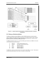
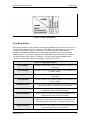
The front panel keypad consists of eight areas, as shown in Figure 4-1 and listed in Table 4-1.
Figure 4-1.
Table 4-1
Item No.
Label
1
MODEM
2
(None)
3
RESET ALARMS
Reset Alarms. This key resets all RCS20 current and latched
major and minor alarms.
4
MODEM SELECT
Select Current Modem. This key selects which modem is
currently being controlled by the Modem group of keys. This
feature is presently not implemented for the RCS20
6
(None)
Numeric Keypad. This group of keys is used to enter numeric
parameters for the RCS20 and connected modems.
7
(None)
Soft keys. This group of keys is used for various functions as
described by the label shown above each key on the last line of
the LCD.
8
SWITCH
4-2
Description
Modem Control. This group of keys is used to control the
modems connected to the RCS20 from the RCS20 front panel.
This feature is presently not implemented for the RCS20
LCD. This is the 8 lines by 40 characters Liquid Crystal Display,
used to communicate with the RCS20.
Switch Control. This group of keys is used to control the RCS20.
TM056 - Rev. 2.3
RCS20 M:N Redundancy Switch
User Interfaces
The ten keys contained in the MODEM and SWITCH are used to view and change a particular set of
control parameters as described by the label next to the key. Each of these keys are used to
display a series of menu trees that are displayed on the LCD and used to view and enter control
parameters. These keys and their corresponding menus are described separately below:
4.1.3.1 MODEM-MOD CONFIG
Pressing this key brings up a series of menus on the LCD that allow control of the currently
selected modulator that is connected to the RCS20. The currently selected modulator and
demodulator can be changed by pressing the MODEM SELECT key. This feature is presently not
implemented on the RCS20
4.1.3.2 MODEM-DEMOD CONFIG
Pressing this key brings up a series of menus on the LCD that allow control of the currently
selected demodulator that is connected to the RCS20. The currently selected modulator and
demodulator can be changed by pressing the MODEM SELECT key. This feature is presently not
implemented on the RCS20
4.1.3.3 MODEM-INTFC CONFIG
Pressing this key brings up a series of menus on the LCD that allow control of the terrestrial
interface for the currently selected modem. The currently selected modem can be change by
pressing the MODEM SELECT key. This feature is presently not implemented on the RCS20.
4.1.3.4 MODEM-MONITOR
Pressing this key brings up a series of menus on the LCD that allow the monitoring of status
parameters for modems connected to the RCS20. This feature is presently not implemented on the
RCS20.
4.1.3.5 MODEM-TEST
Pressing this key brings up a series of menus on the LCD that allow testing of the modems
connected to the RCS20. This feature is presently not implemented on the RCS20.
4.1.3.6 MODEM-ALARMS
Pressing this key brings up a series of menus on the LCD that allow monitoring of alarms for the
modems connected to the RCS20. This feature is presently not implemented on the RCS20.
4.1.3.7 SWITCH-CONFIG SWITCH
Pressing this key brings up a series of menus on the LCD that allow control of the RCS20 switch
configuration parameters.
4.1.3.8 SWITCH-CONFIG SYSTEM
Pressing this key brings up a series of menus on the LCD that allow control of the RCS20 system,
monitor & control, and communication parameters.
TM056 - Rev. 2.3
4-3
User Interfaces
RCS20 M:N Redundancy Switch
4.1.3.9 SWITCH-MONITOR/ALARMS
Pressing this key brings up a series of menus on the LCD that allow monitoring of major and minor
alarms and control of alarm masking for the RCS20.
4.1.3.10 SWITCH-TEST
Pressing this key brings up a series of menus on the LCD that allow testing of the RCS20
configurations and connections.
4.1.4 Front Panel LCD Indicators
There are sixteen (16) LEDs on the RCS20 front panel to indicate the selected LCD menu tree and
current switch status. The color of the illuminated LEDs on the front panel indicate overall switch
status according to the following key: An illuminated green LED indicates normal operation. An
illuminated yellow LED indicates a condition that is not proper for normal operation, however, all
satellite channels are currently on-line. An illuminated red LED indicates that the RCS20 was
unable to provide redundancy protection for a satellite channel, and at least one channel is off-line.
For the purposes of this discussion, the LEDs are separated into two major groups, MENU LEDs
and SWITCH STATUS LEDs. The Menu LEDs are those LEDs immediately next to the front panel
keys in the MODEM and SWITCH groups, and the SWITCH STATUS LEDs are those in the
SWITCH STATUS group (see Table 4-2).
Menu LED Indicators (Green)
Each Menu LED corresponds to the MODEM group or SWITCH group key located to the right of the
LED. When lit these LEDs indicate which menu tree is currently active on the LCD. For example,
if the SWITCH-TEST LED is illuminated, then the LCD is displaying one of the menus that allow
control of RCS20 test modes.
Table 4-2. Switch Status LEDs
LED
Color
Description
Normal
Green
Major Alarm
Red
Minor Alarm
Yellow
Indicates that a redundancy warning exists and the RCS20 may
not be providing redundancy protection.
Test Mode
Yellow
Indicates that the switch is performing one of the system tests.
Event
Yellow
Indicates that a condition of system event as occurred that the
RCS20 has stored in memory. The events may be viewed from
the Front Panel or from the Terminal port.
Remote
Green
Indicates that the unit is set to respond from either the Terminal
port or the Remote M&C port
Indicates that the unit is currently under power.
Indicates that at least one satellite channel did not receive
redundancy protection and is off-line.
4.1.5 Guide to Front Panel Monitor and Control
The front panel can be used to perform complete monitor and configuration of the RCS20. The
operation of the front panel becomes easy after a short period of use in which the user becomes
4-4
TM056 - Rev. 2.3
RCS20 M:N Redundancy Switch
User Interfaces
familiar with the basic concepts and operations. Front panel control is implemented as a series of
data entry screen. The data entry screens (“screens”) are organized into several groups that
contain related parameters and status values. Screens allow the modification of control
parameters, display of status parameters, or both. Different screens will be displayed on the front
panel based on key presses from the front panel. The screens will be displayed in order; this order
defines the ‘menu tree’ for a particular group of related screens. A complete description of control
from the front panel, including explanations of each screen in the menu trees, is found below.
4.2 Remote Port Control
The RCS20 has a dedicated RS485 serial control port (Remote Port) for use with computer
controlled remote monitor and control systems. The Remote Port is a 9-pin female ‘D’ sub
connector J3 located at the rear of the unit on the Switch Interface plug in module. The pinouts for
the remote port are listed in Section 2. The Remote Port utilizes a binary protocol called Radyne
Link Level Protocol (RLLP). RLLP is a multi-drop packet-oriented protocol with handshaking, and is
completely described in Appendix B at the end of this manual. The remote port supports standard
UART asynchronous protocol with 8 data bits, no parity, and 1 stop bit (8N1) at 4 baud rates: 9600,
4800, 2400, and 1200.
4.3 Terminal Port Control
The RCS20 has a dedicated RS232 serial port (Terminal Port) for use with a separate terminal or
computer running a terminal emulation program. The Terminal Port is a 9-pin female ‘D’ sub
connector J2 located at the rear of the unit on the Switch Interface plug in module. The pinouts for
the remote port are listed in Section 2. The terminal port supports standard UART asynchronous
protocol with 8 data bits, no parity, and 1 stop bit (8N1) at 4 baud rates: 19200, 9600, and 2400.
4.3.1 Terminal Interface
The terminal interface is menu driven and allows complete monitoring and control of all RCS20
parameters. A complete listing of all terminal interface configuration menus can be found in
Appendix C at the end of this manual. Three terminal emulation protocols are supported: DEC VT100 , Wyse-50 , and ADDS Viewpoint. The terminal display is a full screen presentation of the
current status of the switch modes and variables. The screens will display both status and control
variables. The status variables cannot be modified, but the control variables can be. Each variable
that can be modified will have a display number next to the value, and changing the value is
accomplished by typing the number of the variable to be changed. Two types of input may then be
requested from the user. If the input is multiple choice, the space key must be pressed to cycle
the available choices until the desired value is displays. The ‘Enter’ or carriage return key must
then be pressed for the new value to take effect. If the input is numerical, the desired value should
be typed using number keys (‘0’ to ‘9’), then pressing the ‘Enter’ key. An input can be aborted at
any time by pressing the ‘ESC’ key. If an invalid value is entered, and error message will be
displayed on the terminal.
4.4 Modem Checkout and Initial Power-up
The following descriptions assume that the RCS20 is installed in a suitable location with AC power
applied to both slide out power supplies. Before initial power-up of the RCS20, the IFS20 and
DDS20 must be connected to the RCU20 via the supplied 15-pin high-density ‘D’ sub connection
cables.
TM056 - Rev. 2.3
4-5
User Interfaces
RCS20 M:N Redundancy Switch
Never apply power to the slide out power supply modules unless they
are firmly seated in the RCU20, as there is a potential shock hazard at
the AC/DC Converter within the module.
Turn the unit on by switching both AC power switches (located above the power entry connectors at
the rear of the RCU20) to the on position. At power-up, the switch processor will perform a selfdiagnostic before beginning the primary monitor/control program. If a failure is detected during the
power-up tests, the Major Alarm LED will illuminate. If there is no failure, there will be no indication
on the front panel.
The initial field checkout of the switch can either be accomplished from the front panel or from a
terminal connected to the Terminal Port. Using a terminal has the advantage of providing full screen
access to all of the switch parameters, but requires a separate terminal or computer with terminal
emulation software. If a terminal is used, the Terminal Port baud rate must first be set from the front
panel.
4.5 RCS20 Front Panel Data Entry Screens
Control from the front panel of the RCS20 is implemented through a series of data entry screens
(“screens”) that are displayed on the front panel LCD. The screens are organized into groups of
related parameters and status values. Within a single group, the screens are displayed on the LCD
in a particular order; this order defines the ‘menu tree’ for that particular group of screen. Each
menu tree is accessed by pressing one of the following keys on the RCS20 front panel:
CONFIG SWITCH, CONFIG SYSTEM, MONITOR/ALARMS, and TEST in the SWITCH group, or
MOD CONFIG, DEMOD CONFIG INTFC CONFIG, MONITOR, TEST and ALARMS in the MODEM
group. For example, pressing the CONFIG SWITCH key causes CONFIG SWITCH SCREEN 0 MODEM CONNECTIONS to be displayed on the LCD (See Figure A-1). The first screen of each
menu tree is called the top screen of that particular menu tree. The menu trees for the SWITCH
group of screens are shown in Figures 3-2, 3-3, 3-4, and 3-5 for the CONFIG SWITCH, CONFIG
SYSTEM, MONITOR/ALARMS, and TEST menu trees respectively.
4.5.1 Basic Front Panel Controls
Once the top screen for a particular menu tree is displayed, either the parameters on the screen
can be edited, the next screen in the menu tree can be displayed, or the previous screen in the
menu tree can be displayed. Each of these actions is discussed in detail below.
4-6
TM056 - Rev. 2.3
RCS20 M:N Redundancy Switch
User Interfaces
4.5.1.1 Changing parameters from the Front Panel
Whenever there is a parameter that can be changed or edited from the front panel, the first
character of the parameter value will highlight with a blinking box. This box is called the cursor,
and the cursor defines what parameter is currently being edited. If there are several parameters on
one screen, two of the soft keys will be labeled <--- and --->. These keys are used to move the
cursor from one parameter to the next, and therefore any of the configuration parameters displayed
on the screen can be edited. The left arrow ( <--- ) moves the cursor to the left, and the right arrow (
---> ) moves the cursor to the right. If the cursor is at the beginning or end of a row containing
several parameters, the cursor will wrap to the opposite side of the display.
Editing a configuration parameter value is accomplished in one of several ways. If the parameter is
numerical, the desired value should be entered from the numeric keys. Occasionally, the numeric
values can be incremented and decremented by pressing soft keys labeled ‘UP’ and ‘DOWN’
respectively. In either case, when all of the numerical parameters have been edited to the desired
values, pressing the ENTER key will execute a load of the parameters into memory, and then
advance to the next screen in the menu tree. Pressing the CLEAR key will not execute a load of
parameters into memory (the original parameter values before editing will be retained), and then
advance to the previous screen in the menu tree.
If a parameter has a non-numeric value, the allowed values for that parameter can be edited by
pressing soft keys with the desired values. In cases where there are multiple parameters shown on
a screen, the values are edited with the soft keys and loaded by pressing the ENTER key, which
also advances to the next screen in the menu tree. Pressing the soft key labeled ‘NEXT’ or
‘PREVIOUS’ will abort loading the parameters into memory, and advance to the appropriate screen.
In cases where there is a single parameter shown on a screen, pressing the soft key labeled with
the desired value will immediately load the parameter into memory. In this case, the parameter load
can be aborted by pressing the CLEAR key, which will return to the previous screen, or by pressing
the soft key labeled ‘NEXT’, which will advance to the next screen in the menu tree.
4.5.1.2 Moving to the Next Screen in a Menu Tree
If the user desires to advance to the next screen in the menu tree, the soft key labeled ‘NEXT’
should be pressed. Some submenu screens can only return to a previous screen, in this case a
soft key will be labeled ‘RETURN’. In either case, if any numerical parameters are being edited, the
values will not be loaded into memory. When the last screen of a menu tree is reached, advancing
to the next screen will wrap to the first screen of the menu tree.
4.5.1.3 Moving to the Previous Screen in a Menu Tree
If the user desires to advance to the previous screen in the menu tree, the CLEAR key should be
pressed. If any numerical parameters are being edited, the values will not be loaded into memory.
If the clear key is pressed while the first screen of a menu tree is displayed, the previous screen will
wrap to the last screen in the menu tree.
TM056 - Rev. 2.3
4-7
User Interfaces
RCS20 M:N Redundancy Switch
4.5.1.4 Summary of Basic Front Panel Controls
Table 4-3 describes the functionality of the front panel keyboard in relation to front panel control.
Table 4-3.
ENTER
Loads edited values into memory and advances to next screen in the menu tree.
CLEAR
Aborts loading values into memory and advances to the previous screen in the
menu tree.
soft key
Aborts loading values into memory and advances to the next screen in the menu
tree.
(‘NEXT’)
soft key
(‘PREVIOUS’)
numeric keys
Aborts loading values into memory and advances to the previous screen in the
menu tree.
Used to edit numeric parameters.
4.6 Front Panel Menu Trees and Screens
There are four menu trees used to control the RCS20: CONFIG SWITCH, CONFIG SYSTEM,
MONITOR/ALARMS, and TEST. These menu trees are shown in flowchart form in Figures 3-2 to 35. Each block in a menu tree flowchart represents a data entry screen, and the arrowed lines
between the blocks represent movement between screens in response to front panel key presses.
Each menu tree diagram is accompanied by a set of figures detailing each data entry screen and
the result of key presses for that data entry screen. The CONFIG SWITCH screens are shown in
Figure 3-x through 3-x, the CONFIG SYSTEM screens are shown in Figures 3-x through 3-x, the
MONITOR/ALARMS screens are shown in Figures 3-x through 3-x, and the TEST screens are
shown in figures 3-x through 3-x. These screen figures are annotated with explanations of the
displayed parameters and details on editing the parameters for each screen.
4-8
TM056 - Rev. 2.3
RCS20 M:N Redundancy Switch
User Interfaces
Figure 4-2.
TM056 - Rev. 2.3
4-9
User Interfaces
RCS20 M:N Redundancy Switch
Figure 4-3.
4-10
TM056 - Rev. 2.3
RCS20 M:N Redundancy Switch
User Interfaces
Figure 4-4.
TM056 - Rev. 2.3
4-11
User Interfaces
RCS20 M:N Redundancy Switch
4.7 Host Computer Remote Communications
Control and status messages are conveyed between the RCS20 and the subsidiary modems and
the host computer using packetized message blocks in accordance with a proprietary
communications specification. This communication is handled by the Radyne Link Level Protocol
(RLLP), which serves as a protocol ‘wrapper’ for the RM&C data. Complete information on monitor
and control software is contained in the Radyne RLLP Protocol Reference Guide.
4.7.1 Protocol Structure
The Communications Specification (COMMSPEC) defines the interaction of computer resident
Monitor and Control software used in satellite earth station equipment such as modems,
redundancy switches, multiplexers, and other ancillary support gear. Communication is bidirectional, and is normally established on one or more full-duplex 9600 baud multi-drop control
buses that conform to EIA Standard RS-485.
Each piece of earth station equipment on a control bus has a unique physical address, which is
assigned during station setup/configuration or prior to shipment. Valid decimal addresses on one
control bus range from 032 through 255 for a total of up to 224 devices per bus. Address 255 of
each control bus is usually reserved for the M&C computer.
4.7.2 Protocol Wrapper
The Radyne COMMSPEC is byte-oriented, with the Least Significant Bit (LSB) issued first. Each
data byte is conveyed as mark/space information with two marks comprising the stop data. When
the last byte of data is transmitted, a hold comprises one steady mark (the last stop bit). To begin
or resume data transfer, a space substitutes this mark. This handling scheme is controlled by the
hardware and is transparent to the user. A pictorial representation of the data and its surrounding
overhead may be shown as follows:
S1
S2
B0
B1
B2
B3
B4
B5
B6
B7
S1
S2,
etc.
The stop bits, S1 and S2, are each a mark. Data flow remains in a hold mode until S2 is replaced
by a space. If S2 is followed by a space, it is considered a start bit for the data byte and not part of
the actual data (B 0 - B 7).
The COMMSPEC developed for use with the Radyne Link Level Protocol (RLLP) organizes the
actual monitor and control data within a shell, or "protocol wrapper", that surrounds the data. The
format and structure of the COMMSPEC message exchanges are described herein. Decimal
numbers have no suffix; hexadecimal numbers end with a lower case h suffix and binary values have
a lower case b suffix. Thus, 22 = 16h = 000010110b. The principal elements of a data frame, in
order of occurrence, are summarized as follows:
<SYN> - the message format header character, or ASCII sync character, that defines the
beginning of a message. The <SYN> character value is always 16h.
<BYTE COUNT> - the Byte Count is the number of bytes in the <DATA> field, ranging from 0
through TBD. This field is 2 bytes long for the DM240 protocol.
<SOURCE ID> - the Source Identifier defines the message originator’s multidrop address. Note
that all nodes on a given control bus have a unique address that must be defined.
4-12
TM056 - Rev. 2.3
RCS20 M:N Redundancy Switch
User Interfaces
<DESTINATION ID> - The Destination Identifier specifies the multidrop address of the device(s) to
which the message is sent.
<FRAME SEQUENCE NUMBER> - The FSN is a tag with a value from 0 through 255 that is sent
with each message. It assures sequential information framing and correct equipment
acknowledgment and data transfers.
<OPCODE> - The Operation Code field contains a number that identifies the message type
associated with the data that follows it. Acknowledgment and error codes are returned in this field.
This field is 2 Bytes for the DM240 protocol.
<...DATA...> - The Data field contains the binary, data bytes associated with the
<OPCODE>. The number of data bytes in this field is indicated by the <BYTE COUNT> value.
<CHECKSUM> - The checksum is the modulo 256 sum of all preceding message bytes, excluding
the <SYN> character. The checksum determines the presence or absence of errors within the
message. In a message block with the following parameters, the checksum is computed as shown
below in Table 4-4.
Table 4-4. Checksum Calculation Example
BYTE FIELD
DATA CONTENT
RUNNING CHECKSUM
<BYTE COUNT> (Byte 1)
00h = 00000000b
00000000b
<BYTE COUNT> (Byte 2)
02h = 00000010b
00000010b
<SOURCEID>
F0h = 11110000b
11110010b
<DESTINATION ID>
2Ah = 00101010b
00011100b
<FSN>
09h = 00001001b
00100101b
<OPCODE> (Byte 1)
00h = 00000000b
00101000b
<OPCODE> (Byte 2)
03h = 00000011b
00101000b
<DATA> (Byte 1)
DFh = 11011111b
00000111b
<DATA> (Byte 2)
FEh = 11111110b
00000101b
Thus, the checksum is 00000101b; which is 05h or 5 decimal. Alternative methods of
calculating the checksum for the same message frame are:
00h + 02h + F0h + 2Ah + 09h + 00h + 03h + DFh + FEh = 305h.
Since the only concern is the modulo 256 (modulo 100h) equivalent (values that can be
represented by a single 8-bit byte), the checksum is 05h.
For a decimal checksum calculation, the equivalent values for each information field are:
0 + 2 + 240 + 42 + 9 + 0 + 3 + 223 + 254 = 773;
773/256 = 3 with a remainder of 5. This remainder is the checksum for the frame.
5 (decimal) = 05h = 0101b = <CHECKSUM>
TM056 - Rev. 2.3
4-13
User Interfaces
RCS20 M:N Redundancy Switch
4.7.3 Frame Description and Bus Handshaking
In a Monitor and Control environment, every message frame on a control bus port executes as a
packet in a loop beginning with a wait-for-SYN-character mode. The remaining message format
header information is then loaded, either by the M&C computer or by a subordinate piece of
equipment requesting access to the bus. Data is processed in accordance with the OPCODE, and
the checksum for the frame is calculated. If the anticipated checksum does not match then the
wait-for-SYN mode goes back into effect. If the OPCODE resides within a command message, it
defines the class of action that denotes an instruction that is specific to the device type, and is a
prefix to the DATA field if data is required. If the OPCODE resides within a query message packet,
then it defines the query code, and can serve as a prefix to query code DATA.
The Frame Sequence Number (FSN) is included in every message packet, and increments
sequentially. When the M & C computer or bus-linked equipment initiates a message, it assigns
the FSN as a tag for error control and handshaking. A different FSN is produced for each new
message from the FSN originator to a specific device on the control bus. If a command packet is
sent and not received at its intended destination, then an appropriate response message is not
received by the packet originator. The original command packet is then re-transmitted with the
same FSN. If the repeated message is received correctly at this point, it is considered a new
message and is executed and acknowledged as such.
If the command packet is received at its intended destination but the response message
(acknowledgment) is lost, then the message originator (usually the M&C computer) re-transmits the
original command packet with the same FSN. The destination device detects the same FSN and
recognizes that the message is a duplicate, so the associated commands within the packet are not
executed a second time. However, the response packet is again sent back to the source as an
acknowledgment in order to preclude undesired multiple executions of the same command.
To reiterate, valid equipment responses to a message require the FSN tag in the command packet.
This serves as part of the handshake/acknowledge routine. If a valid response message is absent,
then the command is re-transmitted with the same FSN. For a repeat of the same command
involving iterative processes (such as increasing or decreasing transmit power level), the FSN is
incremented after each message packet. When the FSN value reaches 255, it overflows and begins
again at zero.
The full handshake/acknowledgment involves a reversal of source and destination ID codes in the
next message frame, followed by a response code in the <OPCODE> field of the message packet
from the equipment under control.
4.7.4 Global Response Operational Codes
In acknowledgment (response) packets, the operational code <OPCODE> field of the message
packet is set to 0 by the receiving devices when the message intended for the device is evaluated
as valid. The devi ce that receives the valid message then exchanges the <SOURCE ID> with the
<DESTINATION ID>, sets the <OPCODE> to zero in order to indicate that a good message was
received, and returns the packet to the originator. This "GOOD MESSAGE" Opcode is one of nine
global responses. Global response Opcodes are common responses, issued to the M&C computer
or to another device, that can originate from and are interpreted by all Radyne ComStream, Inc.
equipment in the same manner. These are summarized as follows (all Opcode values are
expressed in decimal form):
4-14
TM056 - Rev. 2.3
RCS20 M:N Redundancy Switch
User Interfaces
RESPONSE OPCODE DESCRIPTION
OPCODE
Good Message
00h
Bad Parameter
FFh
Bad Opcode
FEh
4.7.5 Collision Avoidance
When properly implemented, the physical and logical devices and ID addressing scheme of the
COMMSPEC normally precludes message packet contention on the control bus. The importance
of designating unique IDs for each device during station configuration cannot be overemphasized.
One pitfall, which is often overlooked, concerns multi-drop override IDs. All too often, multiple
devices of the same type are assigned in a direct-linked ("single-thread") configuration accessible to
the M&C computer directly. For example, if two DM240 Modulators with different addresses
(DESTINATION IDs) are linked to the same control bus at the same hierarchical level, both will
attempt to respond to the M&C computer when the computer generates a multi-drop override ID of
23. If their actual setup parameters, status, or internal timing differs, they will both attempt to
respond to the override simultaneously with different information, or asynchronously in their
respective message packets and response packets, causing a collision on the serial control bus.
To preclude control bus data contention, different IDs must always be assigned to the equipment. If
two or more devices are configured for direct-linked operation, then the M&C computer and all other
devices configured in the same manner must be programmed to inhibit broadcast of the
corresponding multi-drop override ID.
The multi-drop override ID is always accepted by devices of the same type on a common control
bus, independent of the actual DESTINATION ID. These override IDs with the exception of
“BROADCAST” are responded to by all directly linked devi ces of the same type causing contention
on the bus. The “BROADCAST” ID, on the other hand, is accepted by all equipment but none of
them returns a response packet to the remote M&C.
The following multi-drop override IDs are device-type specific, with the exception of "BROADCAST".
These are summarized below with ID values expressed in decimal notation:
TM056 - Rev. 2.3
4-15
User Interfaces
RCS20 M:N Redundancy Switch
Directly-Addressed Equipment
Multi-Drop Override ID
Broadcast (all directly-linked devices)
00
DMD-3000/4000, 4500 or 5000 Mod Section, DMD15
01
DMD-3000/4000, 4500 or 5000 Demod Section, DMD15
02
RCU-340 1:1 Switch
03
RCS-780 1:N Switch
04
RMUX-340 Cross-Connect Multiplexer
05
CDS-780 Clock Distribution System
06
SOM-340 Second Order Multiplexer
07
DMD-4500/5000 Modulator Section
08
DMD-4500/5000 Demodulator Section
09
RCU-5000 M:N Switch
10
DMD15 Modulator
20
DMD15 Demodulator
21
DMD15 Modem
22
DVB3030 Video Modulator, DM240
23
Reserved for future equipment types
24-31
Note that multi-drop override ID 01 can be used interchangeably to broadcast a message to a
DMD-3000/4000 modem, a DMD-4500/5000, a DMD15 modem, or a DVB3030. Radyne
ComStream, Inc. recommends that the multi-drop override IDs be issued only during system
configuration as a bus test tool by experienced programmers, and that they not be included in runtime software. It is also advantageous to consider the use of multiple bus systems where warranted
by a moderate to large equipment complement.
Therefore, if a DMD15 Modulator is queried for its equipment type identifier, it will return a "20" and
DMD15 Demodulator will return a "21". A DMD15 Modem will also return an "22". A DVB3030
Video Modulator will return a “23.”
4.7.6 Software Compatibility
The COMMSPEC, operating in conjunction within the RLLP shell, provides for full forward and
backward software compatibility independent of the software version in use. New features are
appended to the end of the DATA field without OPCODE changes. Older software simply discards
the data as extraneous information without functional impairment for backward compatibility.
If new device-resident or M&C software receives a message related to an old software
version, new information and processes are not damaged or affected by the omission of data.
The implementation of forward and backward software compatibility often, but not always, requires
the addition of new Opcodes. Each new function requires a new Opcode assignment if forward and
backward compatibility cannot be attained by other means.
4-16
TM056 - Rev. 2.3
RCS20 M:N Redundancy Switch
User Interfaces
When Radyne ComStream, Inc. equipment is queried for bulk information (Query Mod, Query
Demod, etc.) it responds by sending back two blocks of data; a Non-Volatile Section (parameters
that can be modified by the user) and a Volatile Section (status information). It also returns a count
value that indicates how large the Non-Volatile Section is. This count is used by M&C developers to
index into the start of the Volatile Section.
When new features are added to Radyne ComStream, Inc. equipment, the control parameters are
appended to the end of the Non-Volatile Section, and status of the features, if any, are added at the
end of the Volatile Section. If a remote M&C queries two pieces of Radyne ComStream, Inc.
equipment with different revision software, they may respond with two different sized packets. The
remote M&C MUST make use of the non-volatile count value to index to the start of the Volatile
Section. If the remote M&C is not aware of the newly added features to the Radyne ComStream,
Inc. product, it should disregard the parameters at the end of the Non-Volatile Section and index to
the start of the Volatile Section.
If packets are handled in this fashion, there will also be backward-compatibility between Radyne
ComStream, Inc. equipment and M&C systems. Remote M&C systems need not be modified every
time a feature is added unless the user needs access to that feature.
4.7.7 RLLP Summary
The RLLP is a simple send-and-wait protocol that automatically re-transmits a packet
when an error is detected, or when an acknowledgment (response) packet is absent.
During transmission, the protocol wrapper surrounds the actual data to form information packets.
Each transmitted packet is subject to time out and frame sequence control parameters, after which
the packet sender waits for the receiver to convey its response. Once a receiver verifies that a
packet sent to it is in the correct sequence relative to the previously received packet, it computes a
local checksum on all information within the packet excluding the <SYN> character and the
<CHECKSUM> fields. If this checksum matches the packet <CHECKSUM>, the receiver
processes the packet and responds to the packet sender with a valid response (acknowledgment)
packet.
The response packet is therefore either an acknowledgment that the message was received
correctly. If the sender receives a valid acknowledgment (response) packet from the receiver, the
<FSN> increments and the next packet is transmitted as required by the sender.
If an acknowledgment (response) packet is lost, corrupted, or not issued due to an error and is
thereby not returned to the sender, the sender re-transmits the original information packet; but with
the same <FSN>. When the intended receiver detects a duplicate packet, the packet is
acknowledged with a response packet and internally discarded to preclude undesired repetitive
executions. If the M&C computer sends a command packet and the corresponding response
packet is lost due to a system or internal error, the computer times out and re-transmits the same
command packet with the same <FSN> to the same receiver and waits once again for an
acknowledgment.
TM056 - Rev. 2.3
4-17
User Interfaces
RCS20 M:N Redundancy Switch
4.7.8 RCS20 Opcode Command Set
The RCS20 Opcode Command Set is listed below:
4-18
Command
Opcode
Query Identification
2403h
Query Control Mode
2404h
Query Switch Status
2001h
Query Switch Configuration
2002h
Query Switch Modem Remote Addresses
2003h
Query Switch Backup Mode
2004h
Query Switch Expansion Module Config
2005h
Query Reference Distribution Configuration
2010h
Query Switch Time
240Eh
Query Switch Date
240Fh
Query Switch Time and Date
2410h
Command Control Mode
2600h
Command Switch Relay Modem Packet
2200h
Command Switch Configuration
2202h
Command Switch Backup Mode
2204h
Command Switch Clear Alarms
2205h
Command Switch Force Manual Backup
2206h
Command Reference Distribution Configuration
2210h
Command Switch Set Time
2C04h
Command Switch Set Date
2C05h
TM056 - Rev. 2.3
RCS20 M:N Redundancy Switch
User Interfaces
4.7.9 RCS20 Channel Definitions
The RCS20 organized the modems connected to the switch according to satellite communications
channels. These channels are labeled on the DDS20 and IFS20 panels, and are defined as follows:
Channel 0
Channel 1
Channel 2
Channel 3
Channel 4
Channel 5
Channel 6
Channel 7
Channel 8
Channel 9
- Backup 1
- Modem 1
- Modem 2
- Modem 3
- Modem 4
- Modem 5
- Modem 6
- Modem 7
- Modem 8
- Modem 9/Backup 2
4.7.10 Detailed Command Descriptions
Refer to Appendix A
4.8 Ethernet Port User Interface
The Ethernet Port of the DM240 allows for complete control and monitoring of all DM240 parameters
and functions via a 10BaseT or 100BaseT Ethernet Connection.
4.9 RCS20 Management Information Base (MIB)
All of the necessary information for the user interface is contained in the DM240 Management
Information Base (MIB), which is contained in Appendix B.
4.10 Terminal Port User Interface
The Terminal Port of the DM240 allows for complete control and monitoring of all DM240 parameters
and functions via an RS-232 Serial Interface.
TM056 - Rev. 2.3
4-19
User Interfaces
4-20
RCS20 M:N Redundancy Switch
TM056 - Rev. 2.3
RCS20 M:N Redundancy Switch
Electrical Interfaces
Section 5 – Electrical Interfaces
5.0 RCS20 Connections
All RCS20 connections are made to labeled connectors located on the rear of the unit. Any
connection interfacing to the RCS20 must be the appropriate mating connector. Refer to Figures 51 through 5-5 for connector locations and Figure 5-6 for the Interconnection Diagram.
Figure 5-1. RCU20 Rear Panel Connectors
TM056 - Rev. 2.3
5-1
Electrical Interfaces
RCS20 M:N Redundancy Switch
Figure 5-2. IFS20 Rear Panel Connectors
5-2
TM056 - Rev. 2.3
RCS20 M:N Redundancy Switch
Electrical Interfaces
Figure 5-3. IFS20 Chassis Base
TM056 - Rev. 2.3
5-3
Electrical Interfaces
RCS20 M:N Redundancy Switch
Figure 5-4. DDS20 Front and Rear Panels
5-4
TM056 - Rev. 2.3
RCS20 M:N Redundancy Switch
Electrical Interfaces
Figure 5-5. Rear Panel Interface – Data Switch Module – DDS20
TM056 - Rev. 2.3
5-5
Electrical Interfaces
RCS20 M:N Redundancy Switch
Figure 5-6. RCS20 Cabling and Interconnection Diagram
5-6
TM056 - Rev. 2.3
RCS20 M:N Redundancy Switch
Electrical Interfaces
5.1 DIP Switch Settings
The following Tables represent the DIP Switch settings for G.703 Balanced, G.703 Unbalanced and
Synchronous (RS-422/V.35) interfaces located on the Digital Data Switch (DDS20).
AS/3356 G.703 Unbalanced
DIP Switch Settings
AS/3356 G.703 Balanced DIP
Switch Settings
AS/3356 ALL SYNC
(RS422/V.35) DIP Switch
Settings
1
ON
1
ON
1
OFF
2
ON
2
ON
2
OFF
3
ON
3
OFF
3
OFF
4
ON
4
OFF
4
OFF
5
ON
5
OFF
5
OFF
6
ON
6
OFF
6
OFF
7
ON
7
ON
7
OFF
8
ON
8
ON
8
OFF
9
ON
9
OFF
9
OFF
10
ON
10
OFF
10
OFF
TM056 - Rev. 2.3
5-7
Electrical Interfaces
RCS20 M:N Redundancy Switch
AS/3478 G.703 Balanced DIP
Switch Settings
5-8
AS/3478 G.703 Balanced DIP
Switch Settings
1
ON
1
OFF
2
ON
2
OFF
3
ON
3
OFF
4
ON
4
OFF
5
ON
5
OFF
6
ON
6
OFF
TM056 - Rev. 2.3
RCS20 M:N Redundancy Switch
Electrical Interfaces
5.2 DDS20 Connector Pinouts
The following connectors are located on the Universal Interface Module on the DDS20. Refer to the
following Tables for the connector pinouts.
5.2.1 J1 - SD - Send Data
J1 is the G.703 Unbalanced Send Data (SD) BNC connector located on the Universal Interface
Module.
5.2.2 J2 - DDO - Drop Data Out
J2 is the Unbalanced Drop Data Out (DDO) BNC connector located on the Universal Interface
Module.
5.2.3 J3 - IDI - Insert Data In
J3 is the Unbalanced Insert Data In (IDI) BNC connector located on the Universal Interface Module.
5.2.4 J4 - RD - Receive Data
J4 is the Unbalanced Receive Data (RD) BNC connector located on the Universal Interface Module.
5.2.5 J5 - ESC Audio
J5 is the 9-pin ‘D’ Female ESC Audio Channel connector. The pinouts for this connector are shown
below in Table 5-1.
Table 5-1. J5 - ESC Audio - 9-Pin ‘D’ Female
Pin No.
Signal
Description
Direction
1
ESCAUD TX 1A
Tx Audio 1A (-)
Input
2
ESCAUDRX 1A
Rx Audio 1A (-)
Output
3
GND
Ground
None
4
ESCAUDTX 2B
Tx Audio 2B (+)
Input
5
ESCAUDRX 2A
Rx Audio 2A (-)
Output
6
ESCAUDTX 1B
Tx Audio 1B (+)
Input
7
ESCAUDRX 1B
Rx Audio 1B (+)
Output
8
ESCAUDTX 2A
Tx Audio 2A (-)
Input
9
ESCAUDRX 2A
Rx Audio 2A (-)
Output
TM056 - Rev. 2.3
5-9
Electrical Interfaces
RCS20 M:N Redundancy Switch
5.2.6 J6 - ES/ES
The connector pinouts for J6, the 9-Pin Earth Station-to-Earth Station asynchronous data connector
are shown Table 5-2.
Table 5-2. J6 - ES/ES - 9-Pin ‘D’ Female
Pin No.
Signal
Description
Direction
1
GND
Ground
None
2
RXD-232
Receive Data RS232
Output
3
TXD-232
Transmit Data RS232
Input
4
TXD-B
Transmit Data RS485 (+)
Input
5
TXD-A
Transmit Data RS485 (-)
Input
6
NC
No Connection
None
7
NC
No Connection
None
8
RXD-B
Receive Data B RS485 (+)
Output
9
RXD-A
Receive Data A RS485 (-)
Output
Table 5–8.
J7 - ESC Alarm Interface - 25-Pin Female ‘D’
Pin Number
5-10
Signal
Description
Direction
1
GND
Ground
None
2
ESCBWO 1 NO
Backward Alarm Out-1 NO
None
3
NC
No Connection
None
4
ESCBWO 1 NO
Backward Alarm Out-2 NO
None
5
NC
No Connection
None
6
ESCBWO 4 NO
Backward Alarm Out-4 NO
None
7
GND
Ground
None
8
ESCBWO 4 NO
Backward Alarm Out-4 NO
None
9
NC
No Connect
None
10
ESCBWI 2
Backward Alarm In 2
Input
11
ESCBWI 4
Backward Alarm In 4
Input
12
NC
No Connect
None
13
NC
No Connect
None
14
ESCBWO 1C
Backward Alarm Out 1-C
None
15
ESCBWO 1-NC
Backward Alarm Out 1-NC
None
TM056 - Rev. 2.3
RCS20 M:N Redundancy Switch
Electrical Interfaces
16
ESCBWO 2-C
Backward Alarm Out 2-C
None
17
ESCBWO 2-NC
Backward Alarm Out 2-NC
None
18
ESCBWO 3-C
Backward Alarm Out 3-C
None
19
ESCBWO 3-NC
Backward Alarm Out 3-NC
None
20
ESCBWO 4-C
Backward Alarm Out 4-C
None
21
ESCBWO 4-NC
Backward Alarm Out 4-NC
None
22
ESCBWI 1
Backward Alarm In 1
Input
23
ESCBWI 1
Backward Alarm In 3
Input
24
NC
No Connection
None
25
NC
No Connect
None
J8 - ESC 8K Data Interface
J8 is the 15-pin ESC IDR 8-Kilobit overhead data connector. The pinouts are shown below.
Table 5-9.
J8 - ESC 8K Data Interface 15-Pin Female ‘D’ Connector
Pin No.
Signal Name
Signal
Direction
1
ESCRXO -B
Rx Octet-B (+)
Output
2
ESCRXC-B
Rx Clock-B (+)
Output
3
ESCRXD-B
Rx Data-B (+)
Output
4
NC
No Connect
None
5
NC
No Connect
None
6
ESCTXD-A
Tx Data-A (-)
Output
7
ESCTXC-A
Tx Clock-A (-)
Output
8
ESCTXO-A
Tx Octet-A (-)
Output
9
ESCRXO -A
Rx Octet-A (-)
Output
10
ESCRXC-A
Rx Clock-A (-)
Output
11
ESCRXD-A
Rx Data-A (-)
Output
12
GND
Ground
None
13
ESCTXD-B
Tx Data-B (+)
Input
14
ESCTXC-B
Tx Clock-B (+)
Output
15
ESCTXO-B
Tx Octet-B (+)
Output
TM056 - Rev. 2.3
5-11
Electrical Interfaces
RCS20 M:N Redundancy Switch
J9- G.703 (Balanced)
J9 is the G.703 (Balanced) 15-pin data connector. The pinouts are shown below.
Table 5-10.
J9 - G.703 (Balanced) 15-Pin Female ‘D’ Connector
Pin No.
Signal Name
Signal
Direction
1
Send Data A (-)
SD-A
Input
9
Send Data B (+)
SD-B
Input
7
External Clock A (-)
BAL EXC-A
Input
8
External Clock B (+)
BAL EXC-B
Input
3
Receive Data A (-)
RD-A
Output
11
Receive Data B (+)
RD-B
Output
12
Drop Data Out A (-)
DDO-A
Output
5
Drop Data Out B (+)
DDO-B
Output
Insert Data In A (-)/EXC A (-)
IDI-A
Input
Insert Data In B (+)/ESC B (+)
IDI-B
Input
13
6
J10 - Sync Data
J10 is the 37-pin synchronous data connector located on the Universal Interface Module. The
pinouts are shown below in Table 5-11.
Table 5–11.
J10 - Sync Data RS422/RS485/V.35 - 37-Pin Female
Pin Number
5-12
Signal
Description
Direction
3
TXO-A
Transmit Octet A (-)
Input
21
TXO-B
Transmit Octet B (+)
Input
4
SD-A
Send Data A (-)
Input
22
SD-B
Send Data B (+)
Input
5
ST-A
Send Timing A (-)
Output
23
ST-B
Send Timing B (+)
Output
6
RD-A
Receive Data A (-)
Output
24
RD-B
Receive Data B (+)
Output
7
RS-A
Request to Send A (-)
Input
25
RS-B
Request to Send B (+)
Input
8
RT-A
Receive Timing A (-)
Output
26
RT-B
Receive Timing B (+)
Output
9
CS-A
Clear to Send A (-)
Output
TM056 - Rev. 2.3
RCS20 M:N Redundancy Switch
Electrical Interfaces
10
MF
Mod Fault - Open
Collector
Output
28
DF
Demod Fault - Open
Collector
Output
27
CS-B
Clear to Send B (+)
Output
11
DM-A
Data Mode A (-)
Output
29
DM-B
Data Mode B (+)
Output
13
RR-A
Receiver Ready A (-)
Output
31
RR-B
Receiver Ready B (+)
Output
15
BAL EXC-A
External Clock A (-)
Input
33
BAL EXC-B
External Clock B (+)
Input
16
RX-0-A
Receive Octet A (-)
Output
34
RX-0 B
Receive Octet B (+)
Output
17
TT-A
Terminal Timing A (-)
Input
35
TT-B
Terminal Timing B (+)
Input
1, 19, 20, 37
GND
Signal Ground
Digital Data Switch (DDS20) J1 through J10 - Switch Connector
J1 through J10 are the 68-Pin high-density data connectors that carry data to and from the modem.
The pinouts for these connectors are shown below in Table 5-12.
Table 5-12.
J18 - Switch Connector - 68-Pin High-Density Female
Pin
No.
Signal
Description
Direction
1
G.703B SD-A
G.703 Send Data Input A (-)
Input
2
SYNC SD-A
Synchronous Data Send Data Input -A (-)
Input
3
ESCBWO 1C
IDR ESC Backward Alarm Out - 1 Common
None
4
G.703B IDI-A
G.703 Insert Data Input - A (-)
Input
5
SYNC ST-A
Synchronous Data Send Timing Output - A
Output
6
ESCBWO 1NO
IDR ESC Backward Alarm Out - 1 Normally
Open
Input
7
SYNC TT-A
Synchronous Data Terminal Timing Input A
Input
8
ESCBWO 2NC
IDR ESC Backward Alarm Out - 2 Normally
Closed
9
DDO-A RT-A
G.703 Drop Data Out A - Synchronous Data
Receive Timing Output - A
TM056 - Rev. 2.3
Output
5-13
Electrical Interfaces
RCS20 M:N Redundancy Switch
10
ESCBWO 3C
IDR ESC Backward Alarm Output - 3
Common
11
IDO-A RD-A
G.703 Insert Data Out A - Synchronous
Data Receive Data A
12
ESCBWO 3NO
IDR ESC Backward Alarm Output - 3
Normally Open
13
BAL EXC-A
External Clock Input - A
14
GND
Ground
15
ESCAUDTX 1A
IDR ESC Audio Input Channel 1A
Input
16
ESCAUDTX 2A
IDR ESC Audio Input Channel 2A
Input
17
ESCAUD RX 1A
IDR ESC Audio Output Channel 1A
Output
18
ESCAUD RX 2A
IDR ESC Audio Output Channel 2A
Output
19
ESCBWI 3
IDR ESC Backward Alarm Input - 3
Input
20
TXD-A BWI 1
IBS ES Transmit Data A
Input
Output
Input
IDR ESC Backward Alarm Input 1
21
MOD FLT
Mod Fault Open Collector Output
Output
Open
Collector
5-14
22
ES RXD-A
IBS ES Receive Data Output - A
Output
23
ES DSR
IBS ES Data Set Ready (RS232 Only)
Output
24
ESCTXC-A
IDR ESC Transmit 8 Kbps Output Clock
Output
25
ESCTXD-A
IDR ESC Transmit 8 Kbps Output Data
Input
26
ESCRXC-A
IDR ESC Receive 8 Kbps Output Clock
Output
27
ESCRXD-A
IDR ESC Receive 8 Kbps Output Data
Output
28
ESCBWO 4NC
IDR ESC Backward Alarm Output - 4
Normally Closed
29
TXO-A
IBS Transmit Octet Input - A
Input
30
SYNC DM-A
Synchronous Data Mode A
Output
31
SYNC CS-A
Synchronous Data Clear to Send - A
Output
32
RXO-A
IBS Receive Octet Output - A
Output
33
SYNC RS-A
Synchronous Data Request to Send A
Input
34
SYNC RR-A
Synchronous Data Receiver Ready - A
Output
35
G703B SD-B
G.703 Send Data Input - B
Input
36
SYNC SD-B
Synchronous Data Send Data Input - B
Input
37
ESCBWO 1 NC
IDR ESC Backward Alarm Out - 1 Normally
Closed
TM056 - Rev. 2.3
RCS20 M:N Redundancy Switch
Electrical Interfaces
38
G703B IDI-B
G.703 Insert Data Input - B
39
SYNC ST-B
Synchronous Data Send Timing Output B
40
ESCBWO 2C
IDR ESC Backward Alarm Out 2 Common
41
SYNC TT-B
Synchronous Data Terminal Timing - B
42
ESCBWO 2NO
IDR ESC Backward Alarm Output 2
Normally Open
43
DDO-B RT-B
G.703 Drop Data Out - B Synchronous Data
Receive Timing B
44
ESCBWO 3NC
IDR ESC Backward Alarm Out - 3 Normally
Closed
45
IDO-B RD-B
G.703 Insert Data Out Synchronous Data
46
ESCBWO 4C
IDR ESC Backward Alarm Out - 4 Common
47
BAL EXC-B
External Clock Input B
48
GND
Ground
49
ESCAUDTX 1B
IDR ESC Audio Input Channel 1B
Input
50
ESCAUDTX 2B
IDR ESC Audio Input Channel 2B
Input
51
ESCAUDRX 1B
IDR ESC Audio Output Channel 1B
Output
52
ESCAUDRX 2B
IDR ESC Audio Output Channel 2B
Output
53
ESCBWI 4
IDR ESC Backward Alarm Input - 4
54
TX-B BWI 2
IBS ES Transmit Data B
Input
Input
IDR ESC Backward Alarm Input 2
55
DMD FLT
Demod Fault Open Collector Output
Output
Open
Collector
56
ES RXD-B
IBS ES Receive Data Input - B
57
GND
Ground
58
ESCTXC-B
IDR ESC Transmit 8 Kbps Output Clock B
Output
59
ESCTXD-B
IDR ESC Transmit 8 Kbps Output Data B
Input
60
ESCRXC-B
IDR ESC Receive 8 Kbps Clock Output B
Output
61
ESCRXD-B
IDR ESC Receive 8 Kbps Data Output B
Output
62
ESCBWO 4NO
IDR ESC Backward Alarm Out - 4 Normally
Open
63
TXO-B
IBS Transmit Octet Input B
Input
64
SYNC DM-B
Synchronous Data - Data Mode Out B
Output
65
SYNC CS-B
Synchronous Data - Clear to Send B
Input
66
RXO-B
IBS Receive Octet Output B
Output
TM056 - Rev. 2.3
Output
5-15
Electrical Interfaces
RCS20 M:N Redundancy Switch
67
SYNC RS-B
Synchronous Data Request to Send - B
Input
68
SYNC RR-B
Synchronous Data Receiver Ready B
Output
RCU20 Connector Pinouts
Table 5-13.
J1 - Switch Interface Control Card - Alarms - 9-pin ‘D’ Male
Pin No.
Signal
Description
Direction
1
MJA-NC
Major Alarm - NC
None
2
MJA-C
Major Alarm - C
None
3
MJA-NO
Major Alarm - NO
None
4
NC
No Connect
None
5
NC
No Connect
None
6
NC
No Connect
None
7
MNA-NC
Minor Alarm - NC
None
8
MNA-C
Minor Alarm - C
None
9
MNA-NO
Minor Alarm - NO
None
Table 5-14.
J2 - Switch Interface Control Card RS232 Terminal Interface - 9-Pin ‘D’ Female
Pin No.
5-16
Signal
Description
Direction
1
NC
No Connect
None
2
RxD
Receive Data
Input
3
TxD
Transmit Data
Output
4
NC
No Connect
None
5
GND
Ground
None
6
NC
No Connect
None
7
NC
No Connect
None
8
NC
No Connect
None
9
NC
No Connect
None
TM056 - Rev. 2.3
RCS20 M:N Redundancy Switch
Electrical Interfaces
Table 5-15.
J3 - Switch Interface Control Card RS485 Remote Interface - 9-Pin ‘D’ Female
Pin No.
Signal
Description
Direction
1
TxD-B
Transmit Data B (+)
Output
2
NC
No Connect
None
3
NC
No Connect
None
4
NC
No Connect
None
5
COMMON
Signal Common
None
6
TxD-A
Transmit Data A (-)
Output
7
NC
No Connect
None
8
RxD-B
Receive Data B (+)
Input
9
RxD-A
Receive Data A (-)
Input
Table 5-16.
J3 - Switch Interface Control Card RS232 Terminal Interface - 9-Pin ‘D’ Female
Pin No.
Signal
Description
Direction
1
NC
No Connect
None
2
RxD
Receive Data
Input
3
TxD
Transmit Data
Output
4
NC
No Connect
None
5
GND
Ground
None
6
NC
No Connect
None
7
NC
No Connect
None
8
NC
No Connect
None
9
NC
No Connect
None
TM056 - Rev. 2.3
5-17
Electrical Interfaces
RCS20 M:N Redundancy Switch
Table 5-17.
J1 - Bank Control Card DDS20 Control and Power - 15-pin HD ‘D’ Female
Pin No.
Signal
Description
Direction
1
DDS_LCLK
Serial Control Clock
Output
2
VCC_RELAY
Relay +6 Volts
Output
3
DDS_LDAT2
Serial Control Data 2
Bi-directional
4
GND
Ground
None
5
GND
Ground
None
6
VCC
Logic +5 Volts
Output
7
VCC_RELAY
Relay +6 Volts
Output
8
VCC_RELAY
Relay +6 Volts
Output
9
GND
Ground
None
10
GND
Ground
None
11
VCC_RELAY
Relay +6 Volts
Output
12
DDS_LDAT1
Serial Control Data 1
Bi-directional
13
GND
Ground
None
14
DDS_LDAT3
Serial Control Data 3
Bi-directional
15
INT
DDS20 Interrupt
Input
Table 5-18.
J2 - Bank Control Card IFS20 Control and Power - 15-pin HD ‘D’ Female
Pin No.
5-18
Signal
Description
Direction
1
IFS_LCLK
Serial Control Clock
Output
2
NC
No Connect
None
3
NC
No Connect
None
4
GND
Ground
None
5
GND
Ground
None
6
VCC
Logic +5 Volts
Output
7
VCC_RELAY
Relay +6 Volts
Output
TM056 - Rev. 2.3
RCS20 M:N Redundancy Switch
Electrical Interfaces
8
NC
No Connect
None
9
NC
No Connect
None
10
GND
Ground
None
11
VCC_RELAY
Relay +6 Volts
Output
12
IFS_LDAT1
Serial Control Data 1
Bi-directional
13
NC
No Connect
None
14
NC
No Connect
None
15
NC
No Connect
None
Table 5-19.
J3 - Bank Control Card RS485 Modem Control - 9-pin ‘D’ Female
Pin No.
Signal
Description
Direction
1
TxD-B
RS485/HDLC Transmit Data B (+)
Output
2
TCLK-A
HDLC Transmit Clock A (-)
Output
3
TCLK-B
HDLC Transmit Clock B (+)
Output
4
RCLK-A
HDLC Receive Clock A (-)
Input
5
COMMON
Signal Common
None
6
TxD-A
RS485/HDLC Transmit Data A (-)
Output
7
RCLK-B
HDLC Receive Clock B (+)
Input
8
RxD-B
RS485/HDLC Receive Data B (+)
Input
9
RxD-A
RS485/HDLC Receive Data A (-)
Input
Table 5-20.
IFS20, J42 - IFS20 Control and Power
15-pin HD ‘D’ Female
Pin No.
Signal
Description
Direction
1
IFS_LCLK
Serial Control Clock
Input
2
NC
No Connect
None
3
NC
No Connect
None
4
GND
Ground
None
5
GND
Ground
None
TM056 - Rev. 2.3
5-19
Electrical Interfaces
5-20
RCS20 M:N Redundancy Switch
6
VCC
Logic +5 Volts
Input
7
VCC_RELAY
Relay +6 Volts
Input
8
NC
No Connect
None
9
NC
No Connect
None
10
GND
Ground
None
11
VCC_RELAY
Relay +6 Volts
Output
12
IFS_LDAT1
Serial Control Data 1
Bi-directional
13
NC
No Connect
None
14
NC
No Connect
None
15
NC
No Connect
None
TM056 - Rev. 2.3
RCS20 M:N Redundancy Switch
Maintenance
Section 6 – Maintenance
6.0 Periodic Maintenance and Troubleshooting
The RCS20 requires no periodic field maintenance procedures. The unit has no adjustments, and
all configuration information is digital and stored in nonvolatile EEPROM. Should a unit be
suspected of a defect in field operations, the proper procedure is to first to follow the basic
troubleshooting guide below. If this does not cure the problem, replace the unit with a known good
unit, if available. If the problem persists with the known good unit, faulty wiring or power should be
suspected. Only minor repairs will be discussed. For serious failures, the user should not attempt
to repair the unit without first contacting Radyne ComStream, Inc. for further information and
instructions.
6.1 Troubleshooting
Upon the detection of an operational failure, the source of the failure must be determined.
Information on system failures will be contained in the Alarms Display. Basic user checks include
checking the power line fuses and the various cables and connectors.
6.1.1 Checking the Cabling and Connectors
Problems that appear difficult to solve can often be traced to a loose or defective cable or connector.
As a first check, the user should check all cables within the system for possible breaks or loose
connections. Cables that are suspect should be replaced. Also check the jacks on the units for
bent or broken pins. Also ensure that both AC power cords are properly plugged into the rear of
the RCS20.
6.1.2 Checking the Fuses
The AC power cord that is next to each fuse must be disconnected before
the fuse may be removed. To keep the RCS20 operational, be sure to
disconnect only one power cord at a time. Also be sure to replace the fuse
and the power cord before checking the other fuse.
The AC fuses are located under the fuse cover next to each AC power plug.
To remove a fuse, the power cord must first be unplugged so that the cover
can be slid away from the fuse and over the AC receptacle. The fuse may
now be removed for testing. Test the fuse with an ohmmeter or similar
device. if necessary, replace the fuse with a new one of the same size and
rating.
TM056 - Rev. 2.3
6-1
Maintenance
RCS20 M:N Redundancy Switch
Each of the slide-in power supply modules houses AC fuses that are
accessible from the rear of the unit. The fuses can be replaced in the field
while maintaining redundancy protection for modems connected to the
RCS20 by changing the fuses for one power supply at a time. Be sure to
replace the fuse with one of the same type and rating. Failure to do so may
result In damage to the equipment and may result In a fire hazard.
6.2 RCS20 Alarms
The RCS20 performs extensive self-monitoring and fault isolation as part of its normal operation.
Any condition that occurs that in not part of the normal operation of the switch result in an alarm
condition, during which the user is notified of the alarm status via the front panel LEDs and the rear
panel Alarm connector (J1 on the Switch Interface Module). The alarms are separated into two
categories: Major Alarms and Minor Alarms. Refer to Table 6-2 and 6-4 for the Major and Minor
Fault Matrices.
6.2.1 Major Alarms
Major Alarms indicate that failure conditions that result in loss of service on one or more primary
satellite channels. A major alarm may be caused by an internal switch hardware failure, by failure
of one or more modems under redundancy protection, or by an incorrect configuration. A Major
Alarm condition is indicated by illumination of the MAJOR ALARM LED on the front panel and by
relay closure on the real panel Alarm connector. All conditions resulting in an RCS20 Major Alarm
are described in Table 6-1 and a Major Alarm matrix is shown in Table 6-2. The alarm matrix shows
all possible alarm conditions, and any actions taken by the RCS20 in response to the alarm.
Table 6-1. RCS20 Major Alarms
RAM/ROM
The RCS20 has detected a failure in either the internal Random
Access Memory, or the Read Only Memory. If this alarm persists,
the unit must be returned to Radyne, Inc. for repair.
BACKUP UNAVAILABLE
The RCS20 attempted to backup a failed prime channel modem, but
no backup channel modem was available because all backup modem
channels are currently in use.
ERROR DURING
BACKUP
The RCS20 attempted to backup a failed prime channel modem, but
there was an error during the backup process that prevented the
backup from going on-line.
6-2
TM056 - Rev. 2.3
RCS20 M:N Redundancy Switch
Maintenance
Table 6-2. Major Alarm Matrix
6.2.2 Minor Alarms
Minor Alarms indicate a failure condition that does not immediately result in loss of service on one
or more primary satellite channels. However, a minor alarm may indicate that there is a loss of
redundancy protection for one or more channels. The RCS20 indicates a Minor Alarm by
illuminating the MINOR ALARM LED on the front panel, and closing a relay on the rear panel
ALARM connector. All conditions resulting in an RCS20 Minor Alarm are described in Table 6-3
and a Minor Alarm matrix is shown in Table 6-4. The alarm matrix shows all possible alarm
conditions, and any actions taken by the RCS20 in response to the alarm.
Table 6-3. RCS20 Minor Alarms
PS 1 PRESENT
The slide in power supply module in position PS1 is missing or not
fully-seated.
PS 1 VOLTAGE
The slide in power supply module in position PS1 is supplying the
incorrect voltage.
PS 2 PRESENT
The slide in power supply module in position PS1 is missing or not
fully seated.
PS 2 VOLTAGE
The slide in power supply module in position PS1 is supplying the
incorrect voltage.
COMMUNICATIONS
One or more of the modems connected to the RCS20 have stopped
responding to remote communications from the switch.
FAULTED PRIME
One or more of the modems connected to the RCS20 that are
designated as prime channels have failed.
FAULTED BACKUP
One or more of the modems connected to the RCS20 that are
designated as backup channels have failed.
CONFIGURATION CHANGE
One or more of the modems connected to the RCS20 that are
designated as prime channels have modem configurations that
have changed while the RCS20 is in automatic switch mode.
CDM CLOCK SLIP
One or more of the clock outputs on a Clock Distribution Module
have lost lock with the external reference.
TM056 - Rev. 2.3
6-3
Maintenance
RCS20 M:N Redundancy Switch
Table 6-2. Major Alarm Matrix
6.2.3 Alarm Masks
Each of the Major and Minor Alarms listed above can be ‘masked’ so that the alarm will not result in
an indication on the front panel LEDs or the ALARM connector. However, the alarm will be
displayed in any of the control modes (Remote, Terminal, or Front Panel). This feature is very
helpful during debugging or system testing to lock out a failure that the user is already aware of. The
alarm masks may be configured from the Front Panel, the Terminal Port, or the Remote Port.
6.2.4 Latched Alarms
Latched Alarms are used to identify intermittent failures in an RCS20 redundancy system. If an
alarm occurs, the alarm condition will be stored even if the condition causing the alarm ceases.
Latched alarms can be displayed and cleared from the Front Panel, the Terminal Port, or the
Remote Port. Note that latched alarms do not show any indication on the front panel LEDs or
ALARM connector. It is recommended that all current and latched alarms be cleared as a final step
after all modems and the RCS20 are configured and running.
6.3 Equipment Return and Repair Procedure
The procedure for returning equipment to Radyne, Inc. for repair is as follows:
1.
Contact Radyne ComStream, Inc. for a Return Material Authorization (RMA) number.
2.
The equipment should be properly packed in its original shipping container, marked with the
RMA Number, and shipped to Radyne ComStream, Inc. freight prepaid.
3.
Radyne ComStream, Inc. will contact the customer when the equipment arrives at the
factory.
6-4
TM056 - Rev. 2.3
RCS20 M:N Redundancy Switch
Maintenance
4.
If the equipment is under warranty, it will be promptly repaired and returned to the user at
no charge (the user pays only the freight charge to the factory). If the equipment is out of
warranty, it will be promptly repaired. The customer will be charged for repairs and return
shipping.
4.
Radyne ComStream, Inc. will notify the customer when the equipment is ready to be
shipped back to their facility.
TM056 - Rev. 2.3
6-5
Maintenance
6-6
RCS20 M:N Redundancy Switch
TM056 - Rev. 2.3
RCS20 M:N Redundancy Switch
Technical Specifiations
Section 7 – Technical Specifications
7.0 Introduction
This section defines the technical performance parameters and specifications for the
RCS20 M:N Redundancy Switch.
7.1 General Specifications
Configurable For:
Online Modulators:
Online Demodulators:
Backup Modulators:
Backup Demodulators:
Uplink Transponders:
Downlink Transponders:
Modes of Operation:
Modulator Switch Time:
Demodulator Switch Time:
Modulator Switch Delay Time:
Demodulator Switch Delay Time:
IF Switching:
1:9, 2:8, 1:4/1:4, 1:2/1:6, 1:3/1:5
1 to 9
1 to 9
1 to 2
1 to 2
1 to 9
1 to 9
Manual, Automatic, Automatic Revertive and Preemptive
250 msec maximum (hot standby), 2.00 sec max (no hot
standby)
250 msec max (hot standby), 2.00 sec max + demod lock
time (no hot standby)
0.0 sec to 299.9 sec, 0.1 sec steps
0.0 sec to 299.9 sec, 0.1 sec steps
Coaxial, 75O, (50O optional), 20 dB return loss
Tx Insertion Loss - 1 dB Nominal
Rx Insertion Loss - 3.5 dB Nominal
7.2 Monitor and Control
Terrestrial Interfaces
Universal I/O (UIO):
User-Selectable RS422/449, G.703, V.35, E1 (G.703), E2
(G.703), T1 and T2
The specifications for the interfaces available on the UIO are as follows:
T1:
E1:
T2:
E2:
ITU V.35:
RS-422/-449:
1.544 Mbps 100O balanced or 75O unbalanced AMI and
B8ZS Line Codes
2.048 Mbps, 120O balanced, or 75O unbalanced HDB3
Line Code.
6.312 Mbps, 110O balanced, B6ZS Line Code or 75O
unbalanced
8.448 Mbps, 75O BNC unbalanced HDB3 Line Code
Differential, Clock and Data Only
All Data Rates, Differential, Clock/Data, DCE
7.3 Options
Clock Distribution Modules, for External Clock.
Cable Sets for DMD15, DMD2400, DVB3000.
ESC Cable Sets
Ethernet Module
TM056 - Rev. 2.3
7-1
Technical Specifications
RCS20 M:N Redundancy Switch
7.4 Power and Environmental
Prime Power:
Operating Temp:
Storage Temp:
100/240 VAC, 50 - 60 Hz, 65 Watts
0 to 50°C, 95% humidity, non-condensing
-20 to 70 degrees C, 99% humidity, non-condensing
7.5 Physical
Size:
Weight:
7-2
RCU20 - 19” W x 19” D x 5.25” H
IFS20 - 19” W x 2” D x 5.25” H
DDS20 - 19” W x 5” D x 8.75” H
RCU20 - 16 lbs. (fully-loaded)
IFS20 - 5 lbs.
DDS20 - 20 lbs.
TM056 – Rev. 2.3
RCS20 M:N Redundancy Switch
Appendix A
Appendix A – Remote RLLP
When new features are added to Radyne ComStream, Inc. equipment, the
control parameters are appended to the end of the Non-Volatile Section of
the Remote Communications Specification, and status of the features, if
any, are added at the end of the Volatile Section. If a remote M&C queries
two pieces of Radyne ComStream, Inc. equipment with different revision
software, they could respond with two different sized packets. The remote
M&C MUST make use of the non-volatile count value to index to the start of
the Volatile Section. If the remote M&C is not aware of the newly added
features to the product, it should disregard the parameters at the end of the
Non-Volatile Section and index to the start of the Volatile Section.
Before creating any software based on the information contained in this
document, contact the Radyne ComStream, Inc. Customer Service
Department (602-437-9620) to find out if the software revision for that piece
of equipment is current and that no new features have been added since
the release of this document.
A.1 Detailed Command Descriptions
Opcode: <2403h>
Query RCS20 Device Identification
Query Response
<1>
Device
Identification
Opcode: <2404h>
24 decimal for RCS20
Query RCS20 Switch Control Mode
Query Response
<1>
Control Mode
0 = Front Panel
1 = Terminal Mode
2 = Remote Port
Opcode: <2001h> Query RCS20 Switch Status
Query Response
<1>
Control Mode
0 = Front Panel
1 = Terminal
2 = Remote Port (Computer RLLP)
<1>
Software
Revision
Binary number, decimal point implied
<1>
Number of
10 decimal for RCS20
TM056 – Rev. 2.3
A-1
Appendix A
RCS20 M:N Redundancy Switch
Channels
<1>
Number of
Status Bytes per
Channels
Maximum number of prime and backup channels available to
the RCS20 switch. 3 decimal for RCS20.
<1>
*Channel 0
Status
Bit 0 = modulator failure flag
Bit 1 = demodulator failure flag
(0 = no failure, 1 = failure)
Bit 2 = switch communication in process
(0 = no comm in process)
(1 = comm in process)
Bit 3 = modem responding to switch flag
(0 = not responding, 1 = responding)
Bit 4 = modulator present
(0= not present, 1= present)
Bit 5 = demodulator present
(0= not present, 1= present)
<1>
*Backed up
Modulator
0 = This channel not a backup channel, or this channel is a
backup channel but currently not backing up a mod
1 - 9 = This channel currently backing up a mod, channel
number as indicated.
<1>
*Backed up
Demodulator
0 = This channel not a backup channel, or this channel is a
backup channel but currently not backing up a demod.
1 - 9 = This channel currently backing up a Demod, channel
number as indicated.
*Note: These 3 bytes repeat for channels 1 - 9 (27
additional bytes used)
A-2
<1>
Switch Major
Alarms
Bit 0 = RAM/ROM fault
Bit 1 = No Backup for Faulted Prime
Bit 2 = Error During Backup
(0 = no alarm, 1 = alarm)
<1>
Switch Minor
Alarms 1
Bit 0 = Power Supply #1 Present
Bit 1 = Power Supply #2 Present
Bit 2 = Power Supply #1 Voltage
Bit 3 = Power Supply #2 Voltage
Bit 4 = Communications Error
Bit 5 = Faulted Prime Modem
Bit 6 = Faulted Backup Modem
Bit 7 = Modem Configuration Change
(0 = no alarm, 1 = alarm)
<1>
Switch Minor
Alarms 2
Bit 0 = CDM Error
Bits 1 - 7: Reserved for future expansion
(0 = no alarm, 1 = alarm)
<1>
Latched Switch
Major Alarms
Bit 0 = RAM/ROM fault
Bit 1 = No Backup for Faulted Prime
TM056 – Rev. 2.3
RCS20 M:N Redundancy Switch
Appendix A
Bit 2 = Error During Backup
(0 = no alarm, 1 = alarm)
<1>
Latched Switch
Minor Alarms 1
Bit 0 = Power Supply #1 Present
Bit 1 = Power Supply #2 Present
Bit 2 = Power Supply #1 Voltage
Bit 3 = Power Supply #2 Voltage
Bit 4 = Communications Error
Bit 5 = Faulted Prime Modem
Bit 6 = Faulted Backup Modem
Bit 7 = Modem Configuration Change
(0 = no alarm, 1 = alarm)
<1>
Latched Switch
Minor Alarms 2
Bit 0 = CDM Error
Bits 1 - 7: Reserved for future expansion
(0 = no alarm, 1 = alarm)
<1>
Backup 1 Mod
Hot Standby
Channel
0 = No hot standby for backup 1 mod
<1>
Backup 1 Demod
Hot Standby
Channel
Channel number (1 to 9)
0 = No hot standby for backup 1 Demod
<1>
Backup 2 Mod
Hot Standby
Channel
<1>
Backup 2 Demod
Hot Standby
Channel
Opcode: <2002h>
Channel number (1 to 8)
0 = No hot standby for backup 2 mod, or channel 9 not
configured as backup
Channel number (1 to 8)
0 = No hot standby for backup 1 Demod, or Channel 9 not
configured as backup
Query RCS20 Switch Configuration
Query Response
<2>
Nonvolatile Bytes
<1>
Number of
Channels
<1>
Nonvolatile Bytes
per Channel
Number of nonvolatile RCS20 configuration memory bytes (125
decimal for RCS20)
Maximum number of prime and backup channels available to
the RCS20 switch. 10 decimal for RCS20.
Number of nonvolatile memory bytes per channel. 10 decimal
for RCS20.
*Channel 0
Configuration
<1>
*Channel 0 Mod
TM056 – Rev. 2.3
Bit 0 = modulator present
Bit 1 = demodulator present
(0 = not present, 1 = present)
A-3
Appendix A
RCS20 M:N Redundancy Switch
Backup Delay
<2>
<2>
0h - BB7h in tenths of a second; decimal point implied
*Channel 0
Demod Backup
Delay
0h - BB7h in tenths of a second; decimal point implied
*Channel 0 Mod
Backup Config
<1>
<1>
*Channel 0
Demod Backup
Config
*Channel 0 Mod
Priority
<1>
Bit 0 = Backup 1 assigned to this modulator
Bit 1 = Backup 2 assigned to this modulator
(0 = not assigned, 1 = assigned)
Bit 0 = Backup 1 assigned to this demodulator
Bit 1 = Backup 2 assigned to this demodulator
(0 = not assigned, 1 = assigned)
Channel 0 Modulator backup priority (0 - 9)
*Channel 0
Demod Priority
<1>
Channel 0 Demodulator backup priority (0 - 9)
*Channel 0
Switch Style
<1>
0 = Switch Mod and Demod separately
1 = Switch Mod and Demod together
Switch Major
Alarm Mask
<1>
Switch Minor
Alarm 1 Mask
<1>
Switch Minor
Alarm 2 Mask
<1>
<1>
A-4
Maximum
Number of
Backup
*Note: These 10 bytes repeat for channels 1 - 9 (uses 90
additional bytes). The Backup Delay applies only to
channels 1 - 9 (the four channel 0 bytes are ignored). If
channel 9 is configured as backup 2, then the four channel
9 Backup Delay bytes are ignored.
Bit 0 = RAM/ROM fault
Bit 1 = No Backup for Faulted Prime
Bit 2 = Error During Backup
(0 = mask, 1 = allow)
Bit 0 = Power Supply #1 Present
Bit 1 = Power Supply #1 Voltage
Bit 2 = Power Supply #2 Present
Bit 3 = Power Supply #2 Voltage
Bit 4 = Communications Error
Bit 5 = Faulted Prime Modem
Bit 6 = Faulted Backup Modem
Bit 7 = Modem Configuration Change
(0 = mask, 1 = allow)
Bit 0 = CDM Error
Bits 1 - 7: Reserved for future expansion.
(0 = mask, 1 = allow)
2 for RCS20
TM056 – Rev. 2.3
RCS20 M:N Redundancy Switch
Appendix A
Channels
<1>
Nonvolatile bytes
per Backup
Channel
4 for RCS20
<1>
Backup 1
(Channel 0)
Configuration
0 = Backup modem
<1>
Backup 1
(Channel 0)
Backup Mode
<1>
Backup 1
(Channel 0)
Force Manual
<1>
Backup 1
(Channel 0)
Force Manual
<1>
Backup 2
(Channel 9)
Configuration
<1>
Backup 2
(Channel 9)
Backup Mode
<1>
Backup 2
(Channel 0)
Force Manual
<1>
Backup 2
(Channel 0)
Force Manual
<4>
0 = Manual
1 = Automatic non-revertive
2 = Automatic revertive
Channel number for manual backup (1 to 9)
Modulator Backup (ignored if in automatic mode)
Channel number for manual backup (1 to 9)
Demodulator Backup (ignored if in automatic mode)
0 = Backup modem
1 = Preemptable prime modem
2 = Prime Modem
0 = Manual
1 = Automatic non-revertive
2 = Automatic revertive
Channel number for manual backup (1 to 8)
Modulator Backup (ignored if in automatic mode or if channel 9
is configured as prime)
Reserved
Channel number for manual backup (1 to 8)
Demodulator Backup (ignored if in automatic mode or if channel
9 is configured as prime)
Reserved
Reserved for RCS10 (= 0 for RCS20)
<4>
Reserved for RCS10 (= 0 for RCS20)
Status Bytes
<1>
Control Mode
0 = Front Panel
1 = Terminal
2 = Remote Port (Computer RLLP)
<1>
Software
Revision
Binary number, decimal point implied
<1>
Number of
Channels
Maximum number of prime and backup channels available to
the RCS20 switch. (10 decimal for RCS20).
TM056 – Rev. 2.3
A-5
Appendix A
RCS20 M:N Redundancy Switch
<1>
Number of
Status Bytes per
Channels
3 decimal for RCS20.
<1>
*Channel 0
Status
Bit 0 = modulator failure flag
Bit 1 = demodulator failure flag
(0 = no failure, 1 = failure)
Bit 2 = switch communication in process
(0 = no comm in process)
(1 = comm in process)
Bit 3 = modem responding to switch flag
(0 = not responding, 1 = responding)
Bit 4 = modulator DDS module present
(0= not present, 1= present)
Bit 5 = demodulator DDS module present
(0= not present, 1= present)
<1>
*Backed up
Modulator
0 = This channel not a backup channel, or this channel is a
backup channel but currently not backing up a mod
1 - 9 = This channel currently backing up a mod, channel
number as indicated.
<1>
*Backed up
Demodulator
0 = This channel not a backup channel, or this channel is a
backup channel but currently not backing up a demod.
1 - 9 = This channel currently backing up Demod, channel
number as indicated.
*Notes: These 3 bytes repeat for channels 1 - 9 (27
additional bytes used)
A-6
<1>
Switch Major
Alarms
Bit 0 = RAM/ROM fault
Bit 1 = No Backup for Faulted Prime
Bit 2 = Error During Backup
(0 = no alarm, 1 = alarm)
<1>
Switch Minor
Alarms 1
Bit 0 = Power Supply #1 Present
Bit 1 = Power Supply #1 Voltage
Bit 2 = Power Supply #2 Present
Bit 3 = Power Supply #2 Voltage
Bit 4 = Communications Error
Bit 5 = Faulted Prime Modem
Bit 6 = Faulted Backup Modem
Bit 7 = Modem Configuration Change
(0 = mask, 1 = allow)
<1>
Switch Minor
Alarms 2
Bits 1 - 7: Reserved for future expansion
(0 = no alarm, 1 = alarm)
<1>
Latched Switch
Major Alarms
Bit 0 = RAM/ROM fault
Bit 1 = No Backup for Faulted Prime
Bit 2 = Error During Backup
TM056 – Rev. 2.3
RCS20 M:N Redundancy Switch
Appendix A
(0 = no alarm, 1 = alarm)
<1>
Latched Switch
Minor Alarms 1
Bit 0 = Power Supply #1 Present
Bit 1 = Power Supply #1 Voltage
Bit 2 = Power Supply #2 Present
Bit 3 = Power Supply #2 Voltage
Bit 4 = Communications Error
Bit 5 = Faulted Prime Modem
Bit 6 = Faulted Backup Modem
Bit 7 = Modem Configuration Change
(0 = mask, 1 = allow)
<1>
Latched Switch
Minor Alarms 2
Bit 0 = CDM Error
Bits 1 - 7: Reserved for future expansion
(0 = no alarm, 1 = alarm)
<1>
Backup 1 Mod
Hot Standby
Channel
Channel number (1 to 9)
0 = No hot standby for backup 1 mod
<1>
Backup 1 Demod
Hot Standby
Channel
Channel number (1 to 9)
0 = No hot standby for backup 1 Demod
<1>
Backup 2 Mod
Hot Standby
Channel
<1>
Backup 2 Demod
Hot Standby
Channel
Opcode: <2003h>
Channel number (1 to 8)
0 = No hot standby for backup 2 mod, or channel 9 not
configured as backup
Channel number (1 to 8)
0 = No hot standby for backup 1 Demod, or Channel 9 not
configured as backup
Query RCS20 Switch Modem Addresses
Query Response
<1>
Number of
Channels
Maximum number of prime and backup channels available to
the RCS20 switch. 10 decimal for RCS20.
<1>
*Modem Address
Modem remote address for channel 0.
* Note: This 1 byte repeats for channels 1 - 9 (uses 9
additional bytes). If a channel is not configured, then
address 0 decimal is returned.
Opcode: <2004h>
Query RCS20 Backup Mode
Query Response
<1>
Maximum
Number of
Backup
Channels
TM056 – Rev. 2.3
2 for RCS20
A-7
Appendix A
RCS20 M:N Redundancy Switch
<1>
Backup 1
(Channel 0)
Backup Mode
0 = Manual
1 = Automatic non-revertive
2 = Automatic revertive
<1>
Backup 2
(Channel 9)
Backup Mode
0 = Manual
1 = Automatic non-revertive
2 = Automatic revertive
(Ignore if Channel 9 is not configured as backup)
Opcode: <2005h>
Query RCS20 Expansion Module Information
Query Response
<1>
Number of
Expansion Slots
6 for RCS20
Each slot returns one byte as follows:
255 decimal = no expansion card present
0 = RCS20 Interface Control Module
1 = RCS20 Bank Control Module
2 = RCS20 Ethernet Interface Module
3 = RCS20 Clock Distribution Module
<1>
Slot 0 Expansion
Card Type
<1>
Slot 1 Expansion
Card Type
<1>
Slot 2 Expansion
Card Type
<1>
Slot 3 Expansion
Card Type
<1>
Slot 4 Expansion
Card Type
<1>
Slot 5 Expansion
Card Type
Opcode: <240Eh>
Query time
Query Response
<1>
Hour
0 - 23
<1>
Minute
0 - 59
<1>
Second
0 - 59
Opcode: <240Fh>
Query date
Query Response
<1>
A-8
Year
0 - 99
TM056 – Rev. 2.3
RCS20 M:N Redundancy Switch
Appendix A
<1>
Month
0 - 11
<1>
Day
0 - 30
Opcode: <2410h>
Query time and date
Query Response
<1>
Year
0 - 99
<1>
Month
0 - 11
<1>
Day
0 - 30
<1>
Hour
0 - 23
<1>
Minute
0 - 59
<1>
Second
0 - 59
Opcode: <2600h>
Set RCS20 Switch Control Mode
<1>
Control Mode
0 = Front Panel
1 = Terminal
2 = Remote Port (Computer RLLP)
Opcode: <2200h> Relay Command or Query to Modem
<1>
Channel Number Channel number for the modem for which the message is to be
relayed (0 to 9 for the RCS20)
RLLP Packet
<n>
from Modem
Complete, addressed RLLP message block with (variable
number of bytes) sync byte, source address, destination
address, Opcode, byte count, data field and checksum.
Contents of Response Packet Data Field: dependent upon
message relayed to modem.
Opcode: <2202h>
Set RCS20 Configuration
<2>
Nonvolatile Bytes Number of nonvolatile RCS20 configuration memory bytes (117
decimal for RCS20)
<1>
Number of
Channels
Maximum number of prime and backup channels available to
the RCS20 switch. (10 decimal) for RCS20.
<1>
Nonvolatile Bytes
per Channel
Number of nonvolatile memory bytes per channel (10 decimal for
RCS20)
<1>
*Channel 0
Configuration
Bit 1 = modulator present
Bit 2 = demodulator present
(0 = not present, 1 = present)
<2>
*Channel 0 Mod
Backup Delay
0h - BB7h in tenths of a second; decimal implied
TM056 – Rev. 2.3
A-9
Appendix A
RCS20 M:N Redundancy Switch
<2>
*Channel 0
Demod Backup
Delay
0h - BB7h in tenths of a second; decimal implied
<1>
*Channel 0 Mod
Backup
Configuration
Bit 0 = Backup 1 assigned to this modulator
Bit 1 = Backup 2 assigned to this modulator
(0 = not assigned, 1 = assigned)
<1>
*Channel 0
Demod Backup
Config
Bit 0 = Backup 1 assigned to this demodulator
Bit 1 = Backup 2 assigned to this demodulator
(0 = not assigned, 1 = assigned)
<1>
*Channel 0 Mod
Priority
Channel 0 Modulator backup priority (0 to 9)
<1>
*Channel 0
Demod Priority
Channel 0 Demodulator backup priority (0 to 9)
<1>
*Channel 0
Switch Style
0 = Switch Mod and Demod separately
1 = Switch Mod and Demod together
*Note: These 10 bytes repeat for channels 1 - 9 (uses 90
additional bytes). The Backup Delay applies only to
channels 1 - 9 (the four channel 0 bytes are ignored). If
channel 9 is configured as backup 2, then the four channel
0 Backup Delay bytes are ignored.
A-10
<1>
Switch Major
Alarm Mask
Bit 0 = RAM/ROM fault
Bit 1 = No Backup for Faulted Prime
(0 = mask, 1 = allow)
<1>
Switch Minor
Alarm 1 Mask
Bit 0 = Power Supply #1 Present
Bit 1 = Power Supply #2 Present
Bit 2 = Power Supply #1 Voltage
Bit 3 = Power Supply #2 Voltage
Bit 4 = Communications Error
Bit 5 = Faulted Prime Modem
Bit 6 = Faulted Backup Modem
Bit 7 = Modem Configuration Change
(0 = mask, 1 = allow)
<1>
Switch Minor
Alarm 2 Mask
Bit 0 = Power Supply #1 Present
(0 = mask, 1 = allow)
<1>
Maximum
Number of
Backup
Channels
2 for RCS20
<1>
Nonvolatile Bytes
per Backup
Channel
4 for RCS20
TM056 – Rev. 2.3
RCS20 M:N Redundancy Switch
Appendix A
<1>
1 (Channel 0)
Configuration
0 = backup modem
<1>
1 (Channel 0)
Backup Mode
0 = manual
1 = automatic non-revertive
2 = automatic revertive
<1>
Backup 1
(Channel 0)
Force Manual
Channel number for manual backup (1 to 9)
Modulator Backup (ignored if in automatic mode)
<1>
Backup 1
(Channel 0)
Force Manual
Channel number for manual backup (1 to 9)
Demodulator Backup (ignored if in automatic mode)
<1>
Backup 2
(Channel 9)
Configuration
0 = backup modem
1 = preemptable prime modem
2 = prime modem
<1>
Backup 2
(Channel 9)
Backup Mode
0 = manual
1 = automatic non-revertive
2 = automatic revertive
<1>
Backup 2
(Channel 0)
Force Manual
Channel number for manual backup (1 to 8)
Modulator Backup (ignored if in automatic mode or if channel 9
is configured as prime)
<1>
Backup 2
(Channel 0)
Force Manual
Channel number for manual backup (1 to 8)
Demodulator Backup (ignored if in automatic mode or if channel
9 is configured as prime)
<4>
Reserved
Reserved for RCS10 (values will be ignored for RCS20)
<4>
Reserved
Reserved for RCS10 (values will be ignored for RCS20)
Opcode: <2204h>
Set RCS20 Backup Mode
<1>
Maximum
2 for RCS20
Number of
Backup
Channels
<1>
Backup 1
(Channel 0)
Backup Mode
0 = Manual
1 = Automatic non-revertive
2 = Automatic revertive
<1>
Backup 2
(Channel 9)
Backup Mode
0 = Manual
1 = Automatic non-revertive
2 = Automatic revertive
(Will be ignored if Channel 9 is not configured as backup)
Opcode: <2205h>
Clear RCS20 Alarms
There is no data field for this command.
TM056 – Rev. 2.3
A-11
Appendix A
RCS20 M:N Redundancy Switch
Opcode: <2206h>
Force RCS20 Manual Backup
<1>
Maximum
2 for RCS20
Number of
Backup
Channels
<1>
<1>
<1>
Backup 1
(Channel 0)
Channel to
Backup
1 to 8 (if Channel 9 configured as backup)
1 to 9 (if Channel 9 not configured as backup)
Backup 2
(Channel 9)
Backup Mode
1 to 8
Notes:
1.
Command will return an error if Backup 1 and
Backup 2 are forced to backup the same channel.
2.
Set channel = 255 decimal if no forced backup is
desired for either backup channel.
3.
Command will return an error if trying to force a
backup for a backup channel not configured in manual
backup mode.
Opcode: <2010h>
Query RCS20 Reference Distribution Module Configuration
<1>
RDM Slot
Slot number on the RCU20 for the RDM to be configured
Number
A-12
<1>
RDM Status
Bit 0 = Ext A Activity
Bit 1 = Ext B Activity
Bit 2 = Internal Ref. Activity
<1>
RDM Fallback
Selection
0 = External A Only
1 = Internal Only
2 = Ext A à Int
3 = Int à Ext A
4 = Ext A à Ext B
5 = Ext A à Ext B à Int
6 = Int à Ext A à Ext B
<1>
RDM Internal
Reference
Frequency
0 = 10 MHz
1 = 5 MHz
2 = 2.5 MHz
3 = 1.25 MHz
<1>
RDM Currently
Selected Source
0 = External A
1 = External B
2 = Internal
TM056 – Rev. 2.3
RCS20 M:N Redundancy Switch
Appendix A
Opcode: <2210h>
Set RCS20 Frequency Distribution Module Configuration
<1>
RDM Slot
Slot number on the RCU20 for the FDM to be configured.
Number
<1>
RDM Fallback
Mode
0
1
2
3
4
5
6
<1>
RDM Internal
Reference
Frequency
0 = 10 MHz
1 = 5 MHz
2 = 2.5 MHz
3 = 1.25 MHz
Opcode: <2C04h>
<1>
Hour
= External A Only
= Internal Only
= Ext A à Int
= Int à Ext A
= Ext A à Ext B
= Ext A à Ext B à Int
= Int à Ext A à Ext B
Command set time
0 - 23
<1>
Minute
0 - 59
<1>
Second
0 - 59
Opcode: <2C05h>
<1>
Year
Command set date
0 - 99
<1>
Month
0 - 11
<1>
Day
0 - 30
Opcode: <2C06h>
<1>
Year
Command set time and date
0 - 99
<1>
Month
0 - 11
<1>
Day
0 – 30
<1>
Hour
0 - 23
<1>
Minute
0 - 59
<1>
Second
0 - 59
TM056 – Rev. 2.3
A-13
Appendix A
A-14
RCS20 M:N Redundancy Switch
TM056 – Rev. 2.3
RCS20 M:N Redundancy Switch
Appendix B
Appendix B – SNMP MIB
-----------------------
___________________________________________________________________________
$RCSfile: hsmmib.txt $
$Revision: 1.8 $
$Date: 2001/06/06 13:56:23 $
$Author: edarosa $
Module Organization :
This is a PRILIMINARY document whose contents are subject to change
without prior notice.
Radyne user MIB Object Identifiers description. The private enterprise
number 2591 is a unique identifier assigned to Radyne by the Internet
Assigned Numbers Authority (IANA). This number is used to uniquely
define vendor specific information such as private MIBs.
Program Units
: (list of program units)
Requirements Trace : (document(s) and paragraph reference)
Deviations
: (any deviations from the coding standard)
Revision History : adapted from 3030/3030L usermib
___________________________________________________________________________
RADYNE-MIB DEFINITIONS ::= BEGIN
IMPORTS
enterprises
FROM RFC1155-SMI
OBJECT-TYPE
FROM RFC-1212;
-- groups in Radyne specific MIB
radyne OBJECT IDENTIFIER ::= { enterprises 2591 }
dvb3030 OBJECT IDENTIFIER ::= { radyne 1 }
radSNMP_Mod_NV_Status OBJECT IDENTIFIER ::= { dvb3030 1 }
radSNMP_Mod_Status OBJECT IDENTIFIER ::= { dvb3030 2 }
radCarrierControl OBJECT-TYPE
SYNTAX INTEGER {
off(0),
on(1)
}
ACCESS read-write
STATUS current
DESCRIPTION
"Turns carrier on and off"
::= { radSNMP_Mod_NV_Status 1 }
radTransmitPower OBJECT-TYPE
SYNTAX INTEGER (-300..50)
ACCESS read-write
STATUS current
DESCRIPTION
"Selects the Tx power level in tenths of dBm
from +5.0 to -20.0 (70/140MHz),
from -5.0 to -30.0 (L-Band).
TM056 – Rev. 2.3
B-1
Appendix B
RCS20 M:N Redundancy Switch
There is an implied decimal point. For example, a value
of 39 represents a transmit power level of +3.9 dBm."
::= { radSNMP_Mod_NV_Status 2 }
radIFFrequency OBJECT-TYPE
SYNTAX INTEGER (50000000..180000000)
ACCESS read-write
STATUS current
DESCRIPTION
"Selects IF frequency in Hz."
::= { radSNMP_Mod_NV_Status 3 }
radDataRate OBJECT-TYPE
SYNTAX INTEGER (0..238000000)
ACCESS read-write
STATUS current
DESCRIPTION
"Selects the data rate in bps. Note: Changing data rate will
affect symbol rate, see comment at the end of mibtext."
::= { radSNMP_Mod_NV_Status 4 }
radSymbolRate OBJECT-TYPE
SYNTAX INTEGER (0..68000000)
ACCESS read-write
STATUS current
DESCRIPTION
"Selects the symbol rate in sps."
::= { radSNMP_Mod_NV_Status 5 }
radSymbolRateMode OBJECT-TYPE
SYNTAX INTEGER {
variable(0),
fixed(1)
}
ACCESS read-write
STATUS optional
DESCRIPTION
"Selects symbol rate mode. This can only be modified if the factory
configuration is set to both variable and fixed.
This is obsolete."
::= { radSNMP_Mod_NV_Status 6 }
radStrapCode OBJECT-TYPE
SYNTAX INTEGER (0..65535)
ACCESS read-write
STATUS optional
DESCRIPTION
"The strap code is a quick set key that sets many modem parameters.
Not implemented."
::= { radSNMP_Mod_NV_Status 7 }
radConvolutionalEncoder OBJECT-TYPE
SYNTAX INTEGER {
none(0),
viterbi1_2(1),
viterbi2_3(2),
viterbi3_4(3),
viterbi5_6(4),
viterbi7_8(5),
viterbi6_7(6),
viterbi8_9(7),
B-2
TM056 – Rev. 2.3
RCS20 M:N Redundancy Switch
Appendix B
}
ACCESS read-write
STATUS current
DESCRIPTION
"Selects Tx code rate and type.
Note: Changing the convolutional encoder will affect symbol rate and
data rate. See note at the end of this section.
Unsupported choices include:
none
viterbi6_7
"
::= { radSNMP_Mod_NV_Status 8 }
radClockControl OBJECT-TYPE
SYNTAX INTEGER {
scte(0),
sct(1),
none(2),
}
ACCESS read-write
STATUS current
DESCRIPTION
"Selects Tx clock source. 0 selects terrestrial clock
(SCTE), 1 selects internal clock (SCT). Modulators using ASI or G.703
interface options must use SCTE at all times."
::= { radSNMP_Mod_NV_Status 9 }
radFramingMode OBJECT-TYPE
SYNTAX INTEGER {
framing_DirecTv (4)
}
ACCESS read-write
STATUS current
DESCRIPTION
"Selects the frame transport stream input type.
Note: Changing the framing mode will affect the symbol rate and/or data
rate. See note at the end of this section."
::= { radSNMP_Mod_NV_Status 10 }
radRolloff OBJECT-TYPE
SYNTAX INTEGER {
rolloff_0_35 (0),
rolloff_0_2 (1),
rolloff_0_25 (25)
}
ACCESS read-write
STATUS current
DESCRIPTION
"0 selects alpha factor rolloff of 0.35,
'1' selects alpha factor rolloff of 0.2,
'25' selects alpha factor rolloff of 0.25"
::= { radSNMP_Mod_NV_Status 11}
radFreqReferenceSource OBJECT-TYPE
SYNTAX INTEGER {
internal(0),
external(1)
}
ACCESS read-write
STATUS current
DESCRIPTION
TM056 – Rev. 2.3
B-3
Appendix B
RCS20 M:N Redundancy Switch
"Selects internal or external reference clock"
::= { radSNMP_Mod_NV_Status 12 }
radExternalReference OBJECT-TYPE
SYNTAX INTEGER (1000000..10000000)
ACCESS read-write
STATUS current
DESCRIPTION
"Selects the external reference frequency in 8 KHz steps."
::= { radSNMP_Mod_NV_Status 13 }
radInterfaceType OBJECT-TYPE
SYNTAX INTEGER {
none(10),
directv(11),
}
ACCESS read-write
STATUS current
DESCRIPTION
"Selects the various interface types.
The following choices are not supported:
none(10),
Note: Selecting interface types Parallel DVB, Parallel M2P, Serial
DirecTv or HSSI will force the outclock selection to SCT. Selecting
interface type ASI Norm or ASI Null causes the outclock selection to
be forced to None.
"
::= { radSNMP_Mod_NV_Status 14 }
radClockPolarity OBJECT-TYPE
SYNTAX INTEGER {
normal(0),
inverted(1)
}
ACCESS read-write
STATUS current
DESCRIPTION
"Selects clock polarity for Tx terrestrial clock relative to Tx data."
::= { radSNMP_Mod_NV_Status 15 }
radDataPolarity OBJECT-TYPE
SYNTAX INTEGER {
normal(0),
inverted(1)
}
ACCESS read-write
STATUS current
DESCRIPTION
"Selects data polarity"
::= { radSNMP_Mod_NV_Status 16}
radSpectrum OBJECT-TYPE
SYNTAX INTEGER {
inverted(0),
normal(1)
}
ACCESS read-write
STATUS current
DESCRIPTION
"Inverts the symbol mapping direction of rotation."
B-4
TM056 – Rev. 2.3
RCS20 M:N Redundancy Switch
Appendix B
::= { radSNMP_Mod_NV_Status 17 }
radModulationType OBJECT-TYPE
SYNTAX INTEGER {
qpsk(0),
bpsk(1),
psk8(2),
qam16(3)
}
ACCESS read-write
STATUS current
DESCRIPTION
"Selects the modulation type.
Note: Changing modulation type will affect the symbol rate and data rate.
See note at the end of this section."
::= { radSNMP_Mod_NV_Status 18}
radFraming OBJECT-TYPE
SYNTAX INTEGER {
dvb(0)
}
ACCESS read-write
STATUS optional
DESCRIPTION
"Selects framing type.
Reserved"
::= { radSNMP_Mod_NV_Status 19 }
radReedsolomon OBJECT-TYPE
SYNTAX INTEGER {
disable(0)
enable(1)
}
ACCESS read-write
STATUS current
DESCRIPTION
"Enables the ReedSolomon encoder. Reserved"
::= { radSNMP_Mod_NV_Status 20 }
radScramblerControl OBJECT-TYPE
SYNTAX INTEGER {
disable(0),
enable(1)
}
ACCESS read-write
STATUS current
DESCRIPTION
"Enables scrambler operation"
::= { radSNMP_Mod_NV_Status 21 }
radScramblerType OBJECT-TYPE
SYNTAX INTEGER {
dvb(0)
}
ACCESS read-write
STATUS optional
DESCRIPTION
"Selects scrambler type.
Not implemented"
::= { radSNMP_Mod_NV_Status 22 }
TM056 – Rev. 2.3
B-5
Appendix B
RCS20 M:N Redundancy Switch
radDifferentialEncoder OBJECT-TYPE
SYNTAX INTEGER {
off(0)
}
ACCESS read-write
STATUS optional
DESCRIPTION
"Disables differential encoder
unsupported
"
::= { radSNMP_Mod_NV_Status 23 }
radAlarmMaskEnable OBJECT-TYPE
SYNTAX INTEGER {
disable(0),
enable(1)
}
ACCESS read-write
STATUS optional
DESCRIPTION
"unsupported"
::= { radSNMP_Mod_NV_Status 24 }
radMajorAlarmMask OBJECT-TYPE
SYNTAX INTEGER (0..255)
ACCESS read-write
STATUS current
DESCRIPTION
"Major Alarm mask:
Bit 1 = Oversample Clock PLL Lock
Bit 2 = FPGA Configuration Error
Bit 3 = Synthesis Clock PLL Lock
Bit 4 = External Reference PLL Lock
"
::= { radSNMP_Mod_NV_Status 25 }
radMinorAlarmMask OBJECT-TYPE
SYNTAX INTEGER (0..255)
ACCESS read-write
STATUS current
DESCRIPTION
"Minor Alarm mask:
Bit 1 = Terrestrial clock activity detect
Bit 2 = Tx data activity detect
Bit 3 = Interleaver FIFO empty error
Bit 5 = Loss of frame synchronization
"
::= { radSNMP_Mod_NV_Status 26 }
radCommonAlarmMask OBJECT-TYPE
SYNTAX INTEGER (0..255)
ACCESS read-write
STATUS current
DESCRIPTION
"Common Alarm mask:
Bit 0 = -12V alarm.
Bit 1 = +12V alarm.
Bit 2 = +5V alarm.
"
::= { radSNMP_Mod_NV_Status 27 }
B-6
TM056 – Rev. 2.3
RCS20 M:N Redundancy Switch
Appendix B
radOperatingMode OBJECT-TYPE
SYNTAX INTEGER {
normal(0),
test_pattern_2_15(1)
}
ACCESS read-write
STATUS current
DESCRIPTION
"Test Pattern Operating Mode:
None,
(2^15)-1
"
::= { radSNMP_Mod_NV_Status 28 }
radCarrierTest OBJECT-TYPE
SYNTAX INTEGER {
off(0),
cw(1),
dual(2),
offset(3),
posfir(4),
negfir(5)
}
ACCESS read-write
STATUS current
DESCRIPTION
"off, turns carrier off
cw, causes the modulator to output pure carrier
dual, causes a double sideband output
offset, causes a single side band output
posfir, uses a positive FIR
negfir, uses a negative FIR"
::= { radSNMP_Mod_NV_Status 29 }
radCircuitID OBJECT-TYPE
SYNTAX OCTET STRING (SIZE (11))
ACCESS read-write
STATUS optional
DESCRIPTION
"Provides entry of Tx circuit identifier. Circuits can be given up
to 11 character alphanumeric identity such as LINK1.
Not implemented."
::= { radSNMP_Mod_NV_Status 30 }
radControlMode OBJECT-TYPE
SYNTAX INTEGER {
local(0),
terminal(1),
computer(2),
ethernet(3)
}
ACCESS read-write
STATUS optional
DESCRIPTION
"Selects the active control source.
This is obsolete."
::= { radSNMP_Mod_NV_Status 31 }
radMode OBJECT-TYPE
SYNTAX INTEGER {
directv(9)
TM056 – Rev. 2.3
B-7
Appendix B
RCS20 M:N Redundancy Switch
}
ACCESS read-write
STATUS current
DESCRIPTION
"Selects the network specification."
::= { radSNMP_Mod_NV_Status 32 }
radInterleaver OBJECT-TYPE
SYNTAX INTEGER {
enable(0),
disable(1)
}
ACCESS read-write
STATUS current
DESCRIPTION
"Enables or disables the interleaver."
::= { radSNMP_Mod_NV_Status 33 }
radOutClockSelection OBJECT-TYPE
SYNTAX INTEGER {
scte(0),
sct(1),
none(2),
}
ACCESS read-write
STATUS current
DESCRIPTION
"Selects the source of clock output from the Terrestrial Interface.
See the Clock Source Selection Matrix."
::= { radSNMP_Mod_NV_Status 34 }
radLastRateControl OBJECT-TYPE
SYNTAX INTEGER {
symbol(0),
data(1),
auto(2)
}
ACCESS read-write
STATUS current
DESCRIPTION
"Allows the modulator to behave with symbol rate or data rate
precedence based on the selection.
See rate control notes."
::= { radSNMP_Mod_NV_Status 35 }
------------------------------------------------------------------------------ Status information out of Radyne specific MIB
radMajorAlarmStatus OBJECT-TYPE
SYNTAX INTEGER (0..255)
ACCESS read-only
STATUS current
DESCRIPTION
"Major Alarm status:
A bit field. 0 = PASS, 1 = FAIL
Bit 1 = Oversample Clock PLL Lock
Bit 2 = FPGA Configuration Error
Bit 3 = Synthesis Clock PLL Lock
Bit 4 = External Reference PLL Lock
"
B-8
TM056 – Rev. 2.3
RCS20 M:N Redundancy Switch
Appendix B
::= { radSNMP_Mod_Status 1 }
radMinorAlarmStatus OBJECT-TYPE
SYNTAX INTEGER (0..255)
ACCESS read-only
STATUS current
DESCRIPTION
"Minor Alarm status:
A bit field. 0 = PASS, 1 = FAIL
Bit 1 = Terrestrial clock activity detect
Bit 2 = Tx data activity detect
Bit 3 = Interleaver FIFO empty error
Bit 5 = Loss of frame synchronization
"
::= { radSNMP_Mod_Status 2 }
radCommonAlarmStatus OBJECT-TYPE
SYNTAX INTEGER (0..255)
ACCESS read-only
STATUS current
DESCRIPTION
"Common Alarm status:
A bit field. 0 = PASS, 1 = FAIL
Bit 0 = -12V alarm.
Bit 1 = +12V alarm.
Bit 2 = +5V alarm.
"
::= { radSNMP_Mod_Status 3 }
radLatchedMajorAlarmStatus OBJECT-TYPE
SYNTAX INTEGER (0..255)
ACCESS read-only
STATUS current
DESCRIPTION
"Major Alarm latched status:
A bit field. 0 = PASS, 1 = FAIL
Bit 1 = Oversample Clock PLL Lock
Bit 2 = FPGA Configuration Error
Bit 3 = Synthesis Clock PLL Lock
Bit 4 = External Reference PLL Lock
"
::= { radSNMP_Mod_Status 4 }
radLatchedMinorAlarmStatus OBJECT-TYPE
SYNTAX INTEGER (0..255)
ACCESS read-only
STATUS current
DESCRIPTION
"Minor Alarm latched status:
A bit field. 0 = PASS, 1 = FAIL
Bit 1 = Terrestrial clock activity detect
Bit 2 = Tx data activity detect
Bit 3 = Interleaver FIFO empty error
Bit 5 = Loss of frame synchronization
"
::= { radSNMP_Mod_Status 5 }
radLatchedCommonAlarmStatus OBJECT-TYPE
SYNTAX INTEGER (0..255)
ACCESS read-only
STATUS current
TM056 – Rev. 2.3
B-9
Appendix B
RCS20 M:N Redundancy Switch
DESCRIPTION
"Common Alarm latched status:
A bit field. 0 = PASS, 1 = FAIL
Bit 0 = -12V alarm.
Bit 1 = +12V alarm.
Bit 2 = +5V alarm.
"
::= { radSNMP_Mod_Status 6 }
radRevisionNumber OBJECT-TYPE
SYNTAX INTEGER (0..255)
ACCESS read-only
STATUS current
DESCRIPTION
"Revision number of the modem firmware with an implied decimal point.
For example, a value of 23 means version number 2.3"
::= { radSNMP_Mod_Status 7 }
radPlus5Volts OBJECT-TYPE
SYNTAX INTEGER (0..255)
ACCESS read-only
STATUS current
DESCRIPTION
"+5V monitor with implied decimal point.
For example, a value of 51 represents +5.1 Volts."
::= { radSNMP_Mod_Status 8 }
radPlus12Volts OBJECT-TYPE
SYNTAX INTEGER (0..255)
ACCESS read-only
STATUS current
DESCRIPTION
"+12V monitor with implied decimal point.
For example, a value of 119 represents +11.9 Volts."
::= { radSNMP_Mod_Status 9 }
radMinus12Volts OBJECT-TYPE
SYNTAX INTEGER (-255..0)
ACCESS read-only
STATUS current
DESCRIPTION
"-12V monitor with implied decimal point.
For example, a value of -122 represents -12.2 Volts."
::= { radSNMP_Mod_Status 10 }
radTemperature OBJECT-TYPE
SYNTAX INTEGER (0..1000)
ACCESS read-only
STATUS current
DESCRIPTION
"Temperature monitor with implied decimal point.
For example, a value of 490 represents 49.0 C"
::= { radSNMP_Mod_Status 11 }
radFactoryConfiguration OBJECT-TYPE
SYNTAX INTEGER (0..65535)
ACCESS read-only
STATUS optional
DESCRIPTION
"A bit field that shows the factory configuration options. 0=No, 1=Yes.
Bit 0 = Serial Interface Present
B-10
TM056 – Rev. 2.3
RCS20 M:N Redundancy Switch
Appendix B
Bit 1 = Parallel Interface
Bit 2 = ASI Norm Interface
Bit 3 = ASI Null Interface
Bit 4 = E3 Interface Present
Bit 5 = T3 Interface Present
Bit 6 = STS-1 Interface Present
Bit 7 = HSSI Interface Present
Bit 8 = DSS Option Enabled
Bit 9 = SNMP Option Enabled
Bit 10 = Parallel DVB Present
Bit 11 = Parallel M2P Present
Bit 12 = DVB LVDS Present
Bit 13 = OC3 Interface Present
Bit 14..15 = Spares
unsupported"
::= { radSNMP_Mod_Status 12 }
radLastRateStatus OBJECT-TYPE
SYNTAX INTEGER {
symbol(0),
data(1),
}
ACCESS read-only
STATUS current
DESCRIPTION
"Shows the current rate precedence. See Last Rate Control notes."
::= { radSNMP_Mod_Status 13 }
END
TM056 – Rev. 2.3
B-11
Appendix B
B-12
RCS20 M:N Redundancy Switch
TM056 – Rev. 2.3
RCS20 M:N Redundancy Switch
Glossary
Glossary
A
A
Ampere
AC
Alternating Current
ADC
Analog to Digital Converter
AGC
Automatic Gain Control
AIS
Alarm Indication System. A signal comprised of all binary 1s.
ANSI
American National Standards Institute
ASCII
American Standard Code for Information Interchange
ASIC
Application Specific Integrated Circuit
ATE
Automatic Test Equipment
B
BER
Bit Error Rate
BERT
Bit Error Rate Test
Bit/BIT
Binary Digit or Built-In Test
BITE
Built-In Test Equipment
bps
Bits Per Second
BPSK
Binary Phase Shift Keying
Byte
8 Binary Digits
C
C
Celsius
CATS
Computer Aided Test Software
CA/xxxx
Cable Assembly
CD-ROM
Compact Disk – Read Only Memory
CLK
Clock
cm
Centimeter
COM
Common
CPU
Central Processing Unit
CRC
Cyclic Redundancy Check. A system of error checking performed at the
transmitting and receiving stations.
CW
Continuous Wave
C/N
Carrier to Noise Ratio
TM056 – Rev. 2.3
G-1
Glossary
RCS20 M:N Redundancy Switch
D
DAC
Digital to Analog Converter
dB
Decibels
dBc
Decibels Referred to Carrier
dBm
Decibels Referred to 1.0 milliwatt
DC
Direct Current
DCE
Data Communications Equipment
Demod
Demodulator or Demodulated
DPLL
Digital Phase Locked Loop
DTE
Data Terminal Equipment
DVB
Digital Video Broadcast
D&I
Drop and Insert
E
Eb/N0
Ratio of Energy per bit to Noise Power Density in a 1 Hz Bandwidth.
EEPROM
Electrically Erasable Programmable Read Only Memory
EIA
Electronic Industries Association
EMI
Electromagnetic Interference
ESC
Engineering Service Circuits
ET
Earth Terminal
F
F
Fahrenheit
FAS
Frame Acquisition Sync. A repeating series bits which allow acquisition of a
frame.
FCC
Federal Communications Commission
FEC
Forward Error Correction
FIFO
First In, First Out
FPGA
Field Programmable Gate Arrays
FW
Firmware
G
g
Force of Gravity
GHz
Gigahertz
GND
Ground
G-2
TM056 – Rev. 2.3
RCS20 M:N Redundancy Switch
Glossary
H
HSSI
High Speed Serial Interface
HW
Hardware
Hz
Hertz (Unit of Frequency)
I
IBS
Intelsat Business Services
IDR
Intermediate Data Rate
I/O
Input/Output
IEEE
International Electrical and Electronic Engineers
IESS
INTELSAT Earth Station Standards
IF
Intermediate Frequency
INTELSAT
International Telecommunication Satellite Organization
ISO
International Standards Organization
J
J
Joule
K
Kbps
Kilobits per Second
Kbps
Kilobytes per Second
kg
Kilogram
kHz
Kilohertz
Ksps
Kilosymbols per Second
L
LCD
Liquid Crystal Display
LED
Light Emitting Diode
LO
Local Oscillator
TM056 – Rev. 2.3
G-3
Glossary
RCS20 M:N Redundancy Switch
M
mA
Milliampere
Mbps
Megabits per Second
MFAS
Multi-Frame Acquisition Sync. See FAS.
MHz
Megahertz
MIB
Management Information Base
Mod
Modulator or Modulated
ms
Millisecond
M&C
Monitor and Control
N
NC
Normally Closed
NO
Normally Open
ns
Nanoseconds
NVRAM
Non-Volatile Random Access Memory
N/C
No Connection or Not Connected
O
OQPSK
Offset Quadrature Phase Shift Keying
P
PC
Personal Computer
PLL
Phase Locked Loop
ppb
Parts per Billion
ppm
Parts per Million
P/N
Part Number
Q
QAM
Quadrature Amplitude Modulation
QPSK
Quadrature Phase Shift Keying
G-4
TM056 – Rev. 2.3
RCS20 M:N Redundancy Switch
Glossary
R
RAM
Random Access Memory
RF
Radio Frequency
ROM
Read Only Memory
rms
Root Mean Square
RU
Rack Unit. 1 RU = 1.75”
Rx
Receive (Receiver)
RxD
Receive Data
R-S
Reed-Solomon Coding. Reed-Solomon codes are block-based error correcting
codes with a wide range of applications in digital communications and storage.
S
SEQ
Sequential
SYNC
Synchronize
T
TBD
To Be Designed or To Be Determined
TM
Technical Manual
TPC
Turbo Product Codes
TRE
Trellis
Tx
Transmit (Transmitter)
TxD
Transmit Data
U
UART
Universal Asynchronous Receiver/Transmitter
UUT
Unit Under Test
V
V
Volts
VAC
Volts, Alternating Current
VCO
Voltage Controlled Oscillator
VDC
Volts, Direct Current
VIT
Viterbi Decoding
TM056 – Rev. 2.3
G-5
Glossary
RCS20 M:N Redundancy Switch
WXYZ
W
Watt
Misc.
µs
Microsecond
O
Ohms
16QAM
16 Quadrature Amplitude Modulation
8PSK
8 Phase Shift Keying
G-6
TM056 – Rev. 2.3