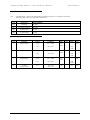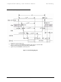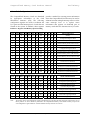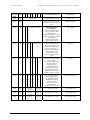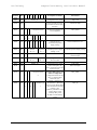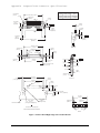
1
CompactFlash™ Memory Card
Product Manual
(Preliminary)
®
CORPORATE HEADQUARTERS
140 Caspian Court
Sunnyvale, CA 94089
408-542-0500
FAX: 408-542-0503
URL: http://www.sandisk.com
SanDisk® Corporation general policy does not recommend the use of its products in life support applications where in a failure or
malfunction of the product may directly threaten life or injury. Per SanDisk Terms and Conditions of Sale, the user of SanDisk
products in life support applications assumes all risk of such use and indemnifies SanDisk against all damages.
The information in this manual is subject to change without notice.
SanDisk Corporation shall not be liable for technical or editorial errors or omissions contained herein; nor for incidental or
consequential damages resulting from the furnishing, performance, or use of this material.
All parts of the SanDisk CompactFlash Memory Card documentation are protected by copyright law and all rights are reserved.
This documentation may not, in whole or in part, be copied, photocopied, reproduced, translated, or reduced to any electronic
medium or machine readable form without prior consent, in writing, from SanDisk Corporation.
SanDisk and the SanDisk logo are registered trademarks of SanDisk Corporation. ImageMate, CompactFlash and CF are
trademarks of SanDisk Corporation.
Product names mentioned herein are for identification purposes only and may be trademarks and/or registered trademarks of
their respective companies.
© 2000 SanDisk Corporation. All rights reserved.
The SanDisk CompactFlash Memory Card is covered or licensed under one or more of the following U.S. Patent Nos. 5,070,032;
5,095,344; 5,168,465; 5,172,338; 5,198,380; 5,200,959; 5,268,318; 5,268,870; 5,272,669; 5,418,752; 5,602,987. Other U.S. and
foreign patents awarded and pending.
Lit. No. 20-10-00038 Rev. 8 9/2001
Printed in U.S.A.
Revision History
• Revisions before Rev. 5—initial release and general changes.
• Revision 5—general editorial changes, CF Type II information added, new higher capacities products added, some lower
capacities removed, new card reader/writer vendor added.
• Revision 6—added new 256 Mbit technology products, general and editorial changes.
• Revision 7—changes to Translate Sector command (page 73) and Device Control Register Enable bit (page 53)
• Revision 8—Removed CF Type II information, added new higher capacity products, removed some lower capacity products,
broadened temperature ranges for 3.3V and 5V operation, modified read & write timing specifications
2
SanDisk CompactFlash Memory Card Product Manual Rev. 8 © 2001 SANDISK CORPORATION
Preliminary
CompactFlash Memory Card Product Manual
Table of Contents
1.0
Introduction to the CompactFlash Memory Card ...................................................................7
1.1
1.2
1.3
1.4
1.5
1.6
1.7
2.0
Product Specifications ..........................................................................................................12
2.1
2.2
2.3
2.4
2.5
2.6
3.0
System Environmental Specifications ..............................................................................................12
System Power Requirements .............................................................................................................12
System Performance ...........................................................................................................................13
System Reliability and Maintenance ................................................................................................13
Physical Specifications........................................................................................................................14
Capacity Specifications.......................................................................................................................16
Installation ............................................................................................................................17
3.1
4.0
Scope .......................................................................................................................................................8
Product Models .....................................................................................................................................8
System Features.....................................................................................................................................9
PCMCIA Standard ................................................................................................................................9
CompactFlash Specification.................................................................................................................9
Related Documentation........................................................................................................................9
Functional Description .........................................................................................................................9
1.7.1
Flash Technology Independence ........................................................................................10
1.7.2
Defect and Error Management............................................................................................10
1.7.3
Wear Leveling .......................................................................................................................10
1.7.4
Using the Erase Sector and Write without Erase Commands ........................................10
1.7.5
Automatic Sleep Mode.........................................................................................................11
1.7.6
Dynamic Adjustment of Performance versus Power Consumption .............................11
1.7.7
Power Supply Requirements...............................................................................................11
Mounting..............................................................................................................................................17
CompactFlash Memory Card Interface Description .............................................................18
4.1
4.2
4.3
Physical Description ...........................................................................................................................18
4.1.1
Pin Assignments and Pin Type ...........................................................................................18
Electrical Description..........................................................................................................................18
Electrical Specification........................................................................................................................25
4.3.1
Input Leakage Current .........................................................................................................25
4.3.2
Input Characteristics.............................................................................................................25
4.3.3
Output Drive Type ...............................................................................................................26
4.3.4
Output Drive Characteristics ..............................................................................................26
4.3.5
Common Memory Read Timing.........................................................................................27
4.3.6
Common and Attribute Memory Write Timing .............................................................28
4.3.6.1
Common Memory Write Timing ......................................................................29
4.3.7
Attribute Memory Read Timing Specification..................................................................29
4.3.8
Attribute Memory Write Timing Specification.................................................................29
4.3.9
Memory Timing Diagrams .................................................................................................30
4.3.10 I/O Read (Input) Timing Specification..............................................................................32
4.3.11 I/O Write (Output) Timing Specification..........................................................................34
SanDisk CompactFlash Memory Card Product Manual Rev. 8 © 2001 SANDISK CORPORATION
3
CompactFlash Memory Card Product Manual
Table of Contents
4.4
4.5
4.6
4.7
5.0
Card Configuration.............................................................................................................................36
4.4.1
Attribute Memory Function ................................................................................................37
4.4.2
Configuration Option Register (Address 200h in Attribute Memory) ..........................38
4.4.3
Card Configuration and Status Register (Address 202h in Attribute Memory) ..........38
4.4.4
Pin Replacement Register (Address 204h in Attribute Memory)...................................39
4.4.5
Socket and Copy Register (Address 206h in Attribute Memory)...................................40
I/O Transfer Function ........................................................................................................................41
4.5.1
I/O Function..........................................................................................................................41
Common Memory Transfer Function...............................................................................................42
4.6.1
Common Memory Function ................................................................................................42
True IDE Mode I/O Transfer Function............................................................................................43
4.7.1
True IDE Mode I/O Function .............................................................................................43
I/O Primary and Secondary Address Configurations...................................................................45
Contiguous I/O Mapped Addressing..............................................................................................46
Memory Mapped Addressing ...........................................................................................................47
True IDE Mode Addressing...............................................................................................................48
ATA Registers......................................................................................................................................49
5.5.1
Data Register (Address - 1F0[170]; Offset 0,8,9) ...............................................................49
5.5.2
Error Register (Address - 1F1[171]; Offset 1, 0Dh Read Only) .......................................50
5.5.3
Feature Register (Address - 1F1[171]; Offset 1, 0Dh Write Only) ..................................50
5.5.4
Sector Count Register (Address - 1F2[172]; Offset 2).......................................................50
5.5.5
Sector Number (LBA 7-0) Register (Address - 1F3[173]; Offset 3)................................50
5.5.6
Cylinder Low (LBA 15-8) Register (Address - 1F4[174]; Offset 4) ................................50
5.5.7
Cylinder High (LBA 23-16) Register (Address - 1F5[175]; Offset 5) .............................50
5.5.8
Drive/Head (LBA 27-24) Register (Address 1F6[176]; Offset 6)....................................51
5.5.9
Status & Alternate Status Registers (Address 1F7[177]&3F6[376]; Offsets 7 & Eh) ....52
5.5.10 Device Control Register (Address - 3F6[376]; Offset Eh) ................................................53
5.5.11 Card (Drive) Address Register (Address 3F7[377]; Offset Fh) .......................................54
ATA Command Description .................................................................................................55
6.1
4
(continued)
ATA Drive Register Set Definition and Protocol.................................................................44
5.1
5.2
5.3
5.4
5.5
6.0
Preliminary
ATA Command Set.............................................................................................................................55
6.1.1
Check Power Mode - 98H, E5H ..........................................................................................57
6.1.2
Execute Drive Diagnostic - 90H ..........................................................................................57
6.1.3
Erase Sector(s) - C0H ............................................................................................................58
6.1.4
Format Track - 50H...............................................................................................................59
6.1.5
Identify Drive - ECH ............................................................................................................59
6.1.5.1
General Configuration........................................................................................61
6.1.5.2
Default Number of Cylinders...........................................................................61
6.1.5.3
Default Number of Heads .................................................................................61
6.1.5.4
Number of Unformatted Bytes per Track........................................................61
6.1.5.5
Number of Unformatted Bytes per Sector .......................................................61
6.1.5.6
Default Number of Sectors per Track...............................................................61
6.1.5.7
Number of Sectors per Card..............................................................................61
6.1.5.8
Memory Card Serial Number............................................................................61
SanDisk CompactFlash Memory Card Product Manual Rev. 8 © 2001 SANDISK CORPORATION
Preliminary
Table of Contents
6.2
7.0
CompactFlash Memory Card Product Manual
(continued)
6.1.5.9
Buffer Type ..........................................................................................................61
6.1.5.10 Buffer Size ............................................................................................................61
6.1.5.11 ECC Count ...........................................................................................................61
6.1.5.12 Firmware Revision..............................................................................................61
6.1.5.13 Model Number ....................................................................................................61
6.1.5.14 Read/Write Multiple Sector Count ..................................................................62
6.1.5.15 Double Word Support ........................................................................................62
6.1.5.16 Capabilities ..........................................................................................................62
6.1.5.17 PIO Data Transfer Cycle Timing Mode ...........................................................62
6.1.5.18 DMA Data Transfer Cycle Timing Mode ........................................................62
6.1.5.19 Translation Parameters Valid............................................................................62
6.1.5.20 Current Number of Cylinders, Heads, Sectors/Track...................................62
6.1.5.21 Current Capacity.................................................................................................62
6.1.5.22 Multiple Sector Setting .......................................................................................62
6.1.5.23 Total Sectors Addressable in LBA Mode .........................................................62
6.1.6
Idle - 97H, E3H ......................................................................................................................63
6.1.7
Idle Immediate - 95H, E1H ..................................................................................................63
6.1.8
Initialize Drive Parameters - 91H .......................................................................................64
6.1.9
Read Buffer - E4H .................................................................................................................64
6.1.10 Read Multiple - C4H.............................................................................................................65
6.1.11 Read Long Sector - 22H, 23H ..............................................................................................66
6.1.12 Read Sector(s) - 20H, 21H ....................................................................................................66
6.1.13 Read Verify Sector(s) - 40H, 41H ........................................................................................67
6.1.14 Recalibrate - 1XH ..................................................................................................................67
6.1.15 Request Sense - 03H..............................................................................................................68
6.1.16 Seek - 7XH..............................................................................................................................69
6.1.17 Set Features - EFH.................................................................................................................69
6.1.18 Set Multiple Mode - C6H .....................................................................................................71
6.1.19 Set Sleep Mode- 99H, E6H...................................................................................................71
6.1.20 Standby - 96H, E2H ..............................................................................................................72
6.1.21 Standby Immediate - 94H, E0H ..........................................................................................72
6.1.22 Translate Sector - 87H ..........................................................................................................73
6.1.23 Wear Level - F5H ..................................................................................................................74
6.1.24 Write Buffer - E8H ................................................................................................................74
6.1.25 Write Long Sector - 32H, 33H .............................................................................................75
6.1.26 Write Multiple Command - C5H ........................................................................................75
6.1.27 Write Multiple without Erase - CDH .................................................................................76
6.1.28 Write Sector(s) - 30H, 31H ...................................................................................................77
6.1.29 Write Sector(s) without Erase - 38H ...................................................................................77
6.1.30 Write Verify Sector(s) - 3CH................................................................................................78
Error Posting ........................................................................................................................................79
CIS Description.....................................................................................................................80
SanDisk CompactFlash Memory Card Product Manual Rev. 8 © 2001 SANDISK CORPORATION
5
CompactFlash Memory Card Product Manual
Table of Contents
Preliminary
(continued)
Ordering Information and Technical Support................................................................................97
Ordering Information....................................................................................................................................99
CompactFlash Memory Card ............................................................................................................99
SanDisk ImageMate™ CompactFlash Drive ...................................................................................99
CompactFlash Memory Card Evaluation Kit..................................................................................99
System Software, Card Reader/Writers and Connectors
Compatible with the SanDisk CompactFlash Memory Cards ...................................................100
Technical Support Services.........................................................................................................................104
Direct SanDisk Technical Support ..................................................................................................104
SanDisk Worldwide Web Site .........................................................................................................104
SanDisk Sales Offices..................................................................................................................105
Appendix CompactFlash Connector Specifications ...................................................................109
Limited Warranty.........................................................................................................................117
6
SanDisk CompactFlash Memory Card Product Manual Rev. 8 © 2001 SANDISK CORPORATION
Preliminary
CompactFlash Memory Card Product Manual
1.0 Introduction to the CompactFlash Memory
Card
The SanDisk CompactFlash™ Memory Card
(CF™) products provide high capacity solid state
flash memory that electrically complies with the
Personal Computer Memory Card International
Association ATA (PC Card ATA) standard. (In
Japan, the applicable standards group is JEIDA.)
The CompactFlash Memory Card Series also
supports a True IDE Mode that is electrically
compatible with an IDE disk drive. CompactFlash
Memory Cards provide up to 512 million bytes
(Megabytes, MBytes or MB) of formatted storage
capacity in the CF Type I form factor. The original
CF form factor card can be used in any system that
has a CF slot, and with a Type II PCMCIA adapter
can be used in any system that has a PCMCIA
Type II or Type III socket.
The CompactFlash Memory Cards use SanDisk
Flash memory which was designed by SanDisk
specifically for use in mass storage applications. In
addition to the mass storage specific Flash memory
chips, the CompactFlash Memory Cards include an
on-card intelligent controller that provides a high
level interface to the host computer. This interface
allows a host computer to issue commands to the
memory card to read or write blocks of memory. A
block of memory consists of 16 Kilobytes of data
and is protected by a powerful Error Correcting
Code (ECC).
The CompactFlash Memory Card on-card
intelligent controller manages interface protocols,
data storage and retrieval as well as ECC, defect
handling and diagnostics, power management and
clock control. Once the CompactFlash Memory
Card has been configured by the host, it appears to
the host as a standard ATA (IDE) disk drive.
Additional ATA commands have been provided to
enhance system performance.
The host system can support as many cards as
there are CompactFlash and PCMCIA Type II or III
card slots. The original form factor CompactFlash
Memory Cards require a PCMCIA Type II Adapter
to be used in a PCMCIA Type II or Type III socket.
SanDisk also offers an industrial version of the
CompactFlash Memory Card Series, which has a
broader operating and non-operating temperature
range than the standard product. Please see Section
2 for detailed specifications.
SanDisk CompactFlash Memory Card Product Manual Rev. 8 © 2001 SANDISK CORPORATION
7
CompactFlash Memory Card Product Manual
Preliminary
Data
In/O ut
Host
Interface
SanDisk
Single
Chip
Controller
SanDisk
Flash
Modules
Control
SanDisk CompactFlash
Figure 1-1 CompactFlash Memory Card Block Diagram
1.1
Scope
1.2
This document describes the key features and
specifications of CompactFlash Memory Cards, as
well as the information required to interface this
product to a host system.
8
Product Models
The CompactFlash Memory Card Series is
available in a variety of capacities as shown in the
following table. All models are shipped formatted
with a DOS file structure.
Standard Model
Industrial Model
Capacity (formatted)
SDCFB-8
SDCFBI-8
8.0 MB
SDCFB-16
SDCFBI-16
16.0 MB
SDCFB-32
SDCFBI-32
32.1 MB
SDCFB-64
SDCFBI-64
64.2 MB
SDCFB-96
SDCFBI-96
96.2 MB
SDCFB-128
SDCFBI-128
128.4 MB
SDCFB-192
SDCFBI-192
192.4 MB
SDCFB-256
SDCFBI-256
256.9 MB
SDCFB-384
SDCFBI-384
384.5 MB
SDCFB-512
SDCFBI-512
512.5 MB
SanDisk CompactFlash Memory Card Product Manual Rev. 8 © 2001 SANDISK CORPORATION
Preliminary
1.3
•
•
•
•
•
•
•
•
•
•
•
•
•
•
•
•
1.4
CompactFlash Memory Card Product Manual
System Features
1.5
Up to 512 MBytes of mass storage data
PC Card ATA protocol compatible
True IDE Mode compatible
Very low CMOS power
Very high performance
Very rugged
Low weight
Noiseless
Low Profile
+5 Volts or +3.3 Volts operation
Automatic error correction and retry capabilities
Supports power down commands and sleep
modes
Non-volatile storage (no battery required)
MTBF >1,000,000 hours
Minimum 10,000 insertions
Standard (SDCFB Series) and Industrial
versions (SDCFBI Series)
CompactFlash Memory Cards are fully compatible
with the CompactFlash Specification published by
the CompactFlash Association. Contact the
CompactFlash Association for more information.
PCMCIA Standard
1.7
CompactFlash Memory Cards are fully electrically
compatible with the PCMCIA specifications listed
below. These specifications may be obtained from:
PCMCIA
2635 North First St., Ste. 209
San Jose, CA 95131
USA
Phone: 408-433-2273
FAX: 408-433-9558
1) PCMCIA PC Card Standard, 7.0, February
1999
2) PCMCIA PC Card ATA Specification, 7.0,
February 1999
CompactFlash Specification
CompactFlash Association
P.O. Box 51537
Palo Alto, CA 94303
USA
Phone: 415-843-1220
FAX: 415-493-1871
www.compactflash.org
1.6
Related Documentation
1) American National Standard X3.221
AT Attachment for Interface for Disk Drives
Document
This document can be ordered from Global
Engineering
Documents
by
calling
1-800-854-7179.
Functional Description
CompactFlash Memory Cards contain a high level,
intelligent subsystem as shown in the block
diagram,
Figure
1-1.
This
intelligent
(microprocessor) subsystem provides many
capabilities not found in other types of memory
cards. These capabilities include:
1) Standard ATA register and command set (same
as found on most magnetic disk drives).
2) Host independence from details of erasing and
programming flash memory.
3) Sophisticated system for managing defects
(analogous to systems found in magnetic disk
drives).
4) Sophisticated system for error recovery
including a powerful error correction code
(ECC).
5) Power management for low power operation.
SanDisk CompactFlash Memory Card Product Manual Rev. 8 © 2001 SANDISK CORPORATION
9
CompactFlash Memory Card Product Manual
1.7.1
Flash Technology Independence
The 512 byte sector size of the CompactFlash
Memory Card is the same as that in an IDE
magnetic disk drive. To write or read a sector (or
multiple sectors), the host computer software
simply issues a Read or Write command to the
CompactFlash Memory Card. This command
contains the address and the number of sectors to
write/read. The host software then waits for the
command to complete. The host software does not
get involved in the details of how the flash
memory is erased, programmed or read. This is
extremely important as flash devices are expected
to get more and more complex in the future. Since
the CompactFlash Memory Card Series uses an
intelligent on-board controller, the host system
software will not require changing as new flash
memory evolves. In other words, systems that
support the CompactFlash Memory Card today
will be able to access future SanDisk cards built
with new flash technology without having to
update or change host software.
1.7.2
Defect and Error Management
1.7.3
Preliminary
Wear Leveling
CompactFlash Memory Card Series products do
not require or perform a Wear Level operation. The
command is supported as a NOP operation to
maintain backward compatibility with existing
software utilities.
1.7.4
Using the Erase Sector and Write without
Erase Commands
As a result of the CompactFlash Card’s high write
performance, the Erase Sector and Write Without
Erase Commands are no longer supported. There
will be no net gain in the use of these commands.
Since the write performance of SanDisk products
typically improves with the introduction of next
generation flash technologies, this feature is no
longer required. Any platforms employing these
commands in previous SanDisk products will not
be affected as a result of the elimination of this
function. The Erase Sector Command will still
erase the sectors but the Write Without Erase
Command will perform a normal Write Command
resulting in no net gain in write performance.
CompactFlash
Memory
Cards
contain
a
sophisticated defect and error management
system. This system is analogous to the systems
found in magnetic disk drives and in many cases
offers enhancements. If necessary, CompactFlash
Memory Cards will reunite data from a defective
sector to a good sector. This is completely
transparent to the host and does not consume any
user data space.
The CompactFlash Memory Card soft error rate
specification is much better than the magnetic disk
drive specification. In the extremely rare case a
read error does occur, CompactFlash Memory
Cards have innovative algorithms to recover the
data.
These defect and error management systems,
coupled with the solid state construction, give
CompactFlash Memory Cards unparalleled
reliability.
10
SanDisk CompactFlash Memory Card Product Manual Rev. 8 © 2001 SANDISK CORPORATION
Preliminary
1.7.5
CompactFlash Memory Card Product Manual
Automatic Sleep Mode
A unique feature of the SanDisk CompactFlash
Memory Card (and other SanDisk products) is
automatic entrance and exit from sleep mode.
Upon
completion
of
a
command,
the
CompactFlash Card will enter sleep mode to
conserve power if no further commands are
received within 5 msec. The host does not have to
take any action for this to occur. In most systems,
the CompactFlash Memory Card is in sleep mode
except when the host is accessing it, thus
conserving power. Note that the delay from
command completion to entering sleep mode can
be adjusted.
When the host is ready to access the CompactFlash
Memory Card and it is in sleep mode, any
command issued to the CompactFlash Card will
cause it to exit sleep and respond. The host does
not have to follow the ATA protocol of issuing a
reset first. It may do this if desired, but it is not
needed. By not issuing the reset, performance is
improved through the reduction of overhead but
this must be done only for the SanDisk products as
other ATA products may not support this feature.
1.7.6
Dynamic Adjustment of Performance versus
Power Consumption
This feature is no longer supported. This command
will be treated as a NOP (No Operation) to
guarantee backward compatibility.
1.7.7
Power Supply Requirements
This is a dual voltage product which means it will
operate at a voltage range of 3.30 volts ± 5% or 5.00
volts ± 10%. Per the PCMCIA specification section
2.1.1, the host system must apply 0 volts in order to
change a voltage range. This same procedure of
providing 0 volts to the card is required if the host
system applies an input voltage outside the desired
voltage by more than 20%. This means less than 4.0
volts for the 5.00 volt range and less than 2.70 volts
for the 3.30 volt range.
SanDisk CompactFlash Memory Card Product Manual Rev. 8 © 2001 SANDISK CORPORATION
11
CompactFlash Memory Card Product Manual
Preliminary
2.0 Product Specifications
For all the following specifications, values are defined
at ambient temperature and nominal supply voltage
unless otherwise stated.
2.1
System Environmental Specifications
Standard Product
(SDCFB)
Industrial Product
(SDCFBI)
Temperature
Operating:
Non-Operating:
0° C to 60° C
-25° C to 85° C
-40° C to 85° C
-50° C to 100° C
Humidity
Operating:
Non-Operating:
8% to 95%, non-condensing
8% to 95%, non-condensing
8% to 95%, non-condensing
8% to 95%, non-condensing
0 dB
0 dB
Acoustic Noise:
Vibration
Operating:
Non-Operating:
15 G peak to peak max.
15 G peak to peak max.
15 G peak to peak max.
15 G peak to peak max.
Shock
Operating:
Non-Operating:
2,000 G max.
2,000 G max.
2,000 G max.
2,000 G max.
Altitude (relative to sea level)
Operating:
Non-Operating:
80,000 feet max.
80,000 feet max.
80,000 feet max.
80,000 feet max.
2.2
System Power Requirements
Standard Product
(SDCFB)
DC Input Voltage (VCC)
100 mV max. ripple (p-p)
+5 V Currents
(maximum Average value)
See Notes 1 to 3.
Note 1.
Note 2.
Note 3.
12
Sleep:
Reading:
Writing:
Read/Write Peak
Industrial Product
(SDCFBI)
3.3V ±5%
5V ± 10%
3.3V ±5%
5V ±10%
200 µA
(Slow - Fast)
21 mA - 45 mA
21 mA - 60 mA
150 mA/50µs
500 µA
(Slow - Fast)
34 mA - 75 mA
34 mA - 90 mA
150 mA/50µs
200 µA
(Slow - Fast)
21 mA - 45 mA
21 mA - 60 mA
150 mA/50µs
500 µA
(Slow - Fast)
34 mA - 75 mA
34 mA - 90 mA
150 mA/50µs
All values quoted are typical at ambient temperature and nominal supply voltage unless otherwise stated.
Sleep mode currently is specified under the condition that all card inputs are statis CMOS levels and in a “Not Busy“
operating state.
The currents specified show the bounds of programmability of the product.
SanDisk CompactFlash Memory Card Product Manual Rev. 8 © 2001 SANDISK CORPORATION
Preliminary
2.3
CompactFlash Memory Card Product Manual
System Performance
All performance timings assume the CompactFlash
Memory Card Series controller is in the default
(i.e., fastest) mode.
Start Up Times
Sleep to write:
Sleep to read:
Reset to ready:
Active to Sleep Delay
2.5 msec maximum
2.0 msec maximum
50 msec typical
400 msec maximum
Programmable
Data Transfer Rate
To/From Flash
20.0 MBytes/sec burst
Data Transfer Rate
To/From Host
16.0 MBytes/sec burst
Controller Overhead
Command to DRQ
50 msec maximum
Note:
The Sleep to Write and Sleep to Read times are the times it takes the CompactFlash Memory Card to exit sleep mode
when any command is issued by the host to when the card is reading or writing. CompactFlash Memory Cards do not
require a reset to exit sleep mode. See section 1.7.5.
2.4
System Reliability and Maintenance
MTBF (@ 25°C)
>1,000,000 hours
Preventive Maintenance
None
Data Reliability
<1 non-recoverable error in 1014 bits read, 1 erroneous
correction in 1020 bits read
Endurance SDCFB-XX
≥300,000 erase / program cycles per block typical
SDCFBI-XX Industrial Temp
≥100,000 erase / program cycles per block typical
SanDisk CompactFlash Memory Card Product Manual Rev. 8 © 2001 SANDISK CORPORATION
13
CompactFlash Memory Card Product Manual
2.5
Preliminary
Physical Specifications
Refer to the following table and to Figure 2-1 for
CompactFlash
Memory
Card
physical
specifications and dimensions.
CompactFlash
Weight: 11.4 g (.40 oz) typical
14.2 g (.50 oz) maximum
Length: 36.40 ± 0.15 mm (1.433 ±.006 in)
Width: 42.80 ± 0.10 mm (1.685 ±.004 in)
Thickness: 3.3 mm ± 0.10 mm (.130 ±.004 in) (Excluding Lip)
.039±.002
[1.00]
25
.040±.003
[1.00]
2X .118±.003
[3.00]
P
TO
.096±.003
[2.4]
[36.40]
1
.040±.003
[1.00]
2X 1.015±.003
[25.78]
[12.00]
.130±.004
[3.30]
2X .472±.004
50
26
1.433±.006
.063±.002
[1.60]
.030±.003
[0.8]
1.640±.005 [41.66]
4X R.020±.004
[0.5]
1.685±.004
[42.80]
.025±.003
[0.6]
Figure 2-1 CompactFlash Memory Card Dimensions
14
SanDisk CompactFlash Memory Card Product Manual Rev. 8 © 2001 SANDISK CORPORATION
Preliminary
CompactFlash Memory Card Product Manual
Refer to the following table and to Figure 2-2 for CompactFlash Memory Card PC Card Adapter physical
specifications and dimensions.
CF Adapter
Weight: 33 g (1.16 oz) typical
Length: 85.6 ± 0.20 mm (3.370 ±.008 in)
Width: 54.0 ± 0.10 mm (2.126 ±.004 in)
Thickness: 5.0 mm Max (0.1968 in)
0.196
[5.0]
0.130
[3.3]
2.126
[54.0]
3.370
[85.6]
1.196
[30.4]
.866
[22.0]
1.536
[39.03]
.472
[12.0]
.078
[2.0]
1.694
[43.03]
0.138
[3.5]
Figure 2-2 CompactFlash Memory Card Adapter Dimensions
SanDisk CompactFlash Memory Card Product Manual Rev. 8 © 2001 SANDISK CORPORATION
15
CompactFlash Memory Card Product Manual
2.6
Preliminary
Capacity Specifications
The table below shows the specific capacity for the
various models and the default number of heads,
sectors/track and cylinders.
16
Model Number
Capacity
(formatted)
Sectors/Card
(Max LBA+1)
No. of
Heads
No. of
Sectors/
Track
No. of
Cylinders
SDCFB-8
8,028,160 bytes
15,680
2
32
245
SDCFB-16
16,056,320 bytes
31,360
2
32
490
SDCFB-32
32,112,640 bytes
62,720
4
32
490
SDCFB-64
64,225,280 bytes
125,440
8
32
490
SDCFB-128
128,450,560 bytes
250,880
8
32
980
SDCFB-192
192,413,696 bytes
375,808
16
32
734
SDCFB-256
256,901,120 bytes
501,760
16
32
980
SDCFB-384
384,491,520 bytes
750,960
16
63
745
SDCFB-512
512,483,328 bytes
1,000,944
16
63
993
SanDisk CompactFlash Memory Card Product Manual Rev. 8 © 2001 SANDISK CORPORATION
Preliminary
CompactFlash Memory Card Product Manual
3.0 Installation
3.1
Mounting
The CompactFlash Memory Card may be installed
in any platform with a 50 position Surface Mount
Interface Header (3M P/N N7E50-7516VY-20) and
Ejector (3M P/N D7E50-7316-02), or equivalent,
properly installed. Refer to the appendix at the end
of this manual for additional technical information.
In addition, the CompactFlash Memory Card may
be used in any standard PCMCIA Type II (5 mm)
or Type III (10.5 mm) socket as supplied by an
OEM using a Type II PCMCIA adapter.
SanDisk CompactFlash Memory Card Product Manual Rev. 8 © 2001 SANDISK CORPORATION
17
CompactFlash Memory Card Product Manual
Preliminary
4.0 CompactFlash Memory Card Interface
Description
4.1
Physical Description
The host is connected to the CompactFlash
Memory Card using a standard 50 pin connector
consisting of two rows of 25 female contacts each
on 50 mil (1.27 mm) centers.
4.1.1
Pin Assignments and Pin Type
The signal/pin assignments are listed in Table 4-1.
Low active signals have a “-” prefix. Pin types are
Input, Output or Input/Output. Table 4-2 defines
the DC characteristics for all input and output type
structures.
18
4.2
Electrical Description
The CompactFlash Memory Card Series is
optimized for operation with hosts which support
the PCMCIA I/O interface standard conforming to
the PC Card ATA specification. However, the
CompactFlash Card may also be configured to
operate in systems that support only the memory
interface standard. The configuration of the
CompactFlash Card will be controlled using the
standard PCMCIA configuration registers starting
at address 200h in the Attribute Memory space of
the CompactFlash Memory Card.
Table 4-2 describes the I/O signals. Signals whose
source is the host are designated as inputs while
signals that the CompactFlash Memory Card
sources are outputs. The CompactFlash Card logic
levels conform to those specified in the PCMCIA
Release 2.1 specification. Refer to section 4.3 for
definitions of Input and Output type.
SanDisk CompactFlash Memory Card Product Manual Rev. 8 © 2001 SANDISK CORPORATION
Preliminary
CompactFlash Memory Card Product Manual
Table 4-1 Pin Assignments and Pin Type
PC Card Memory Mode
Pin
Num
Signal
Name
1
GND
2
D03
3
PC Card I/O Mode
4
True IDE Mode
4
Pin
Num
Signal
Name
Ground
1
GND
I/O
I1Z,OZ3
2
D03
I/O
I1Z,OZ3
D04
I/O
I1Z,OZ3
3
D04
I/O
I1Z,OZ3
4
D05
I/O
I1Z,OZ3
4
D05
I/O
I1Z,OZ3
I1Z,OZ3
5
D06
I/O
I1Z,OZ3
5
D06
I/O
I1Z,OZ3
I/O
I1Z,OZ3
6
D07
I/O
I1Z,OZ3
6
D07
I/O
I1Z,OZ3
I
I3U
7
-CE1
I
I3U
7
-CS0
I
I3Z
2
In, Out
Type
Pin
Num
Signal
Name
Ground
1
GND
I/O
I1Z,OZ3
2
D03
D04
I/O
I1Z,OZ3
3
4
D05
I/O
I1Z,OZ3
5
D06
I/O
6
D07
7
-CE1
Pin
Type
Pin
Type
In, Out4
Type
In, Out
Type
Pin
Type
Ground
8
A10
I
I1Z
8
A10
I
I1Z
8
A10
I
I1Z
9
-OE
I
I3U
9
-OE
I
I3U
9
-ATA SEL
10
11
A09
I
A08
I
12
A07
13
VCC
14
15
16
I
A06
I
A05
I
A04
I
I1Z
I1Z
10
11
A09
I
A08
I
I1Z
12
A07
Power
13
VCC
I1Z
I1Z
I1Z
14
15
16
I
A06
I
A05
I
A04
I
I1Z
I1Z
10
11
I
I3U
2
I
I1Z
2
I
I1Z
2
I
I1Z
A09
A08
I1Z
12
A07
Power
13
VCC
14
2
I
I1Z
2
I
I1Z
2
I
I1Z
2
I1Z
I1Z
I1Z
15
16
A06
A05
A04
Power
17
A03
I
I1Z
17
A03
I
I1Z
17
A03
I
I1Z
18
A02
I
I1Z
18
A02
I
I1Z
18
A02
I
I1Z
19
A01
I
I1Z
19
A01
I
I1Z
19
A01
I
I1Z
20
A00
I
I1Z
20
A00
I
I1Z
20
A00
I
I1Z
21
D00
I/O
I1Z,OZ3
21
D00
I/O
I1Z,OZ3
21
D00
I/O
I1Z,OZ3
22
D01
I/O
I1Z,OZ3
22
D01
I/O
I1Z,OZ3
22
D01
I/O
I1Z,OZ3
23
D02
I/O
I1Z,OZ3
23
D02
I/O
I1Z,OZ3
23
D02
I/O
I1Z,OZ3
24
WP
O
OT3
24
-IOIS16
O
OT3
24
-IOCS16
O
ON3
25
-CD2
O
Ground
25
-CD2
O
Ground
25
-CD2
O
Ground
26
-CD1
O
Ground
26
-CD1
O
Ground
26
-CD1
O
Ground
27
1
27
D11
1
27
D11
1
I/O
I1Z,OZ3
D12
1
D12
1
I/O
I1Z,OZ3
D13
1
D13
1
I/O
I1Z,OZ3
D14
1
D14
1
I/O
I1Z,OZ3
D15
1
D15
1
I/O
I1Z,OZ3
1
I
I3Z
28
29
30
31
D11
1
D12
1
D13
1
D14
1
D15
I/O
I/O
I/O
I/O
I/O
I1Z,OZ3
I1Z,OZ3
I1Z,OZ3
I1Z,OZ3
I1Z,OZ3
32
1
-CE2
I
I3U
33
-VS1
O
34
-IORD
I
28
29
30
31
I/O
I/O
I/O
I/O
I/O
I1Z,OZ3
I1Z,OZ3
I1Z,OZ3
I1Z,OZ3
I1Z,OZ3
28
29
30
31
32
-CE2
1
I
I3U
32
-CS1
Ground
33
-VS1
O
Ground
33
-VS1
O
Ground
I3U
34
-IORD
I
I3U
34
-IORD
I
I3Z
SanDisk CompactFlash Memory Card Product Manual Rev. 8 © 2001 SANDISK CORPORATION
19
CompactFlash Memory Card Product Manual
Preliminary
Table 4-1 Pin Assignments and Pin Type (continued)
PC Card Memory Mode
PC Card I/O Mode
True IDE Mode
Pin
Num
Signal
Name
Pin
Type
In, Out
Type
Pin
Num
Signal
Name
Pin
Type
In, Out
Type
Pin
Num
Signal
Name
Pin
Type
In, Out4
Type
35
-IOWR
I
I3U
35
-IOWR
I
I3U
35
-IOWR
I
I3Z
36
-WE
I
I3U
36
-WE
I
I3U
36
-WE3
I
I3U
37
RDY/BSY
O
OT1
37
IREQ
O
OT1
37
INTRQ
O
OZ1
38
VCC
Power
38
VCC
Power
38
VCC
39
-CSEL
I
I2Z
39
-CSEL
I
I2Z
39
-CSEL
I
I2U
40
-VS2
O
OPEN
40
-VS2
O
OPEN
40
-VS2
O
OPEN
41
RESET
I
I2Z
41
RESET
I
I2Z
41
-RESET
I
I2Z
42
-WAIT
O
OT1
42
-WAIT
O
OT1
42
IORDY
O
ON1
43
-INPACK
O
OT1
43
-INPACK
O
OT1
43
-INPACK
O
OZ1
44
-REG
I
45
BVD2
I/O
46
BVD1
I/O
47
48
D08
1
D09
1
49
D10
50
GND
Note:
20
1
I/O
I/O
I/O
4
I3U
4
3
Power
44
-REG
I
I3U
44
-REG
I
I3U
I1U,OT1
45
-SPKR
I/O
I1U,OT1
45
-DASP
I/O
I1U,ON1
I1U,OT1
46
-STSCHG
I/O
I1U,OT1
46
-PDIAG
I1Z,OZ3
I1Z,OZ3
47
48
D08
1
D09
1
1
I1Z,OZ3
49
D10
Ground
50
GND
I/O
I/O
I/O
I1Z,OZ3
I1Z,OZ3
47
48
I/O
I1U,ON1
D08
1
I/O
I1Z,OZ3
D09
1
I/O
I1Z,OZ3
1
I/O
I1Z,OZ3
I1Z,OZ3
49
D10
Ground
50
GND
Ground
1. These signals are required only for 16 bit access and not required when installed in 8-bit systems.
For lowest power dissipation, leave these signals open.
2. Should be grounded by the host.
3. Should be tied to VCC by the host.
4. Please refer to section 4.3 for definitions of In, Out type.
SanDisk CompactFlash Memory Card Product Manual Rev. 8 © 2001 SANDISK CORPORATION
Preliminary
CompactFlash Memory Card Product Manual
Table 4-2 Signal Description
Signal Name
Dir.
A10 - A0
(PC Card Memory Mode)
I
Pin
8, 10, 11, 12, 14, These address lines along with the -REG signal are used to select the
following: The I/O port address registers within the CompactFlash
15, 16, 17, 18,
Card, the memory mapped port address registers within the card, a
19, 20
byte in the card's information structure and its configuration control
and status registers.
A10 - A0
(PC Card I/O Mode)
A2 - A0
(True IDE Mode)
This signal is the same as the PC Card Memory Mode signal.
I
18, 19, 20
In True IDE Mode only A[2:0] are used to select the one of eight
registers in the Task File.
In True IDE Mode, these remaining address lines should be grounded
by the host.
A10 - A3
(True IDE Mode)
BVD1
(PC Card Memory Mode)
Description
I/O
46
This signal is asserted high as the BVD1 signal since a battery is not
used with this product.
-STSCHG
(PC Card I/O Mode)
Status Changed
This signal is asserted low to alert the host to changes in the RDY/BSY and Write Protect states, while the I/O interface is configured. Its
use is controlled by the Card Config and Status Register.
-PDIAG
(True IDE Mode)
In the True IDE Mode, this input / output is the Pass Diagnostic signal
in the Master / Slave handshake protocol.
BVD2
(PC Card Memory Mode)
I/O
45
This output line is always driven to a high state in Memory Mode
since a battery is not required for this product.
-SPKR
(PC Card I/O Mode)
This output line is always driven to a high state in I/O Mode since this
product does not support the audio function.
-DASP
(True IDE Mode)
In the True IDE Mode, this input/output is the Disk Active/Slave
Present signal in the Master/Slave handshake protocol.
-CD1, -CD2
(PC Card Memory Mode)
O
26, 25
These Card Detect pins are connected to ground on the CompactFlash
Card. They are used by the host to determine if the card is fully
inserted into its socket.
-CD1, -CD2
(PC Card I/O Mode)
This signal is the same for all modes.
-CD1, -CD2
(True IDE Mode)
This signal is the same for all modes.
-CE1, -CE2
(PC Card Memory Mode)
Card Enable
I
7, 32
These input signals are used both to select the card and to indicate to
the card whether a byte or a word operation is being performed. -CE2
always accesses the odd byte of the word. -CE1 accesses the even byte
or the Odd byte of the word depending on A0 and -CE2. A multiplexing scheme based on A0, -CE1, -CE2 allows 8 bit hosts to access
all data on D0-D7. See Tables 4-11, 4-12, 4-15, and 4-16.
-CE1, -CE2
(PC Card I/O Mode)
Card Enable
This signal is the same as the PC Card Memory Mode signal.
-CS0, -CS1
(True IDE Mode)
In the True IDE Mode -CS0 is the chip select for the task file registers
while -CS1 is used to select the Alternate Status Register and the
Device Control Register.
SanDisk CompactFlash Memory Card Product Manual Rev. 8 © 2001 SANDISK CORPORATION
21
CompactFlash Memory Card Product Manual
Preliminary
Table 4-2 Signal Description (continued)
Signal Name
Dir.
Pin
Description
-CSEL
(PC Card Memory Mode)
I
39
This signal is not used for this mode.
-CSEL
(PC Card I/O Mode)
This signal is not used for this mode.
-CSEL
(True IDE Mode)
This internally pulled up signal is used to configure this device as a
Master or a Slave when configured in the True IDE Mode. When this
pin is grounded, this device is configured as a Master. When the pin is
open, this device is configured as a Slave.
D15 - D00
(PC Card Memory Mode)
31, 30, 29, 28, These lines carry the Data, Commands and Status information between
the host and the controller. D00 is the LSB of the Even Byte of the
27, 49, 48, 47, 6,
Word. D08 is the LSB of the Odd Byte of the Word.
5, 4, 3, 2, 23,
22, 21
D15 - D00
(PC Card I/O Mode)
This signal is the same as the PC Card Memory Mode signal.
D15 - D00
(True IDE Mode)
In True IDE Mode, all Task File operations occur in byte mode on the
low order bus D00-D07 while all data transfers are 16 bit using D00D15.
GND
(PC Card Memory Mode)
--
1, 50
Ground.
GND
(PC Card I/O Mode)
This signal is the same for all modes.
GND
(True IDE Mode)
This signal is the same for all modes.
-INPACK
( PC Card Memory Mode)
O
43
This signal is not used in this mode.
-INPACK
( PC Card I/O Mode)
Input Acknowledge
The Input Acknowledge signal is asserted by the CompactFlash Card
when the card is selected and responding to an I/O read cycle at the
address that is on the address bus. This signal is used by the host to
control the enable of any input data buffers between the card and the
CPU.
-INPACK
(True IDE Mode)
In True IDE Mode this output signal is not used and should not be
connected at the host.
-IORD
(PC Card Memory Mode)
22
I/O
I
34
This signal is not used in this mode.
-IORD
(PC Card I/O Mode)
This is an I/O Read strobe generated by the host. This signal gates I/O
data onto the bus from the CompactFlash Card when the card is
configured to use the I/O interface.
-IORD
(True IDE Mode)
In True IDE Mode, this signal has the same function as in PC Card I/O
Mode.
SanDisk CompactFlash Memory Card Product Manual Rev. 8 © 2001 SANDISK CORPORATION
Preliminary
CompactFlash Memory Card Product Manual
Table 4-2 Signal Description (continued)
Signal Name
Dir.
Pin
Description
-IOWR
(PC Card Memory Mode)
I
35
This signal is not used in this mode.
-IOWR
(PC Card I/O Mode)
The I/O Write strobe pulse is used to clock I/O data on the Card Data
bus into the CompactFlash controller registers when the card is
configured to use the I/O interface.
The clocking will occur on the negative to positive edge of the signal
(trailing edge).
-IOWR
(True IDE Mode)
-OE
(PC Card Memory Mode)
In True IDE Mode, this signal has the same function as in PC Card I/O
Mode.
I
9
This is an Output Enable strobe generated by the host interface. It is
used to read data from the CompactFlash Card in Memory Mode and
to read the CIS and configuration registers.
-OE
(PC Card I/O Mode)
In PC Card I/O Mode, this signal is used to read the CIS and
configuration registers.
-ATA SEL
(True IDE Mode)
To enable True IDE Mode this input should be grounded by the host.
RDY/-BSY
(PC Card Memory Mode)
O
37
In Memory Mode this signal is set high when the CompactFlash Card
is ready to accept a new data transfer operation and held low when the
card is busy. The Host memory card socket must provide a pull-up
resistor.
At power up and at Reset, the RDY/-BSY signal is held low (busy)
until the CompactFlash Card has completed its power up or reset
function. No access of any type should be made to the CompactFlash
Card during this time. The RDY/-BSY signal is held high (disabled
from being busy) whenever the following condition is true: The
CompactFlash Card has been powered up with +RESET continuously
disconnected or asserted.
-IREQ
( PC Card I/O Mode)
I/O Operation - After the CompactFlash Card has been configured for
I/O operation, this signal is used as -Interrupt Request. This line is
strobed low to generate a pulse mode interrupt or held low for a level
mode interrupt.
INTRQ
(True IDE Mode)
In True IDE Mode signal is the active high Interrupt Request to the
host.
-REG
(PC Card Memory Mode)
Attribute Memory Select
I
44
This signal is used during Memory Cycles to distinguish between
Common Memory and Register (Attribute) Memory accesses. High for
Common Memory, Low for Attribute Memory.
-REG
(PC Card I/O Mode)
The signal must also be active (low) during I/O Cycles when the I/O
address is on the Bus.
-REG
(True IDE Mode)
In True IDE Mode this input signal is not used and should be
connected to VCC by the host.
SanDisk CompactFlash Memory Card Product Manual Rev. 8 © 2001 SANDISK CORPORATION
23
CompactFlash Memory Card Product Manual
Preliminary
Table 4-2 Signal Description (continued)
Signal Name
Dir.
Pin
Description
RESET
(PC Card Memory Mode)
I
41
When the pin is high, this signal resets the CompactFlash Card. The
card is Reset only at power up if this pin is left high or open from
power-up. The card is also reset when the Soft Reset bit in the Card
Configuration Option Register is set.
RESET
(PC Card I/O Mode)
This signal is the same as the PC Card Memory Mode signal.
-RESET
(True IDE Mode)
In the True IDE Mode this input pin is the active low hardware reset
from the host.
VCC
(PC Card Memory Mode)
13, 38
+5 V, +3.3 V power.
VCC
(PC Card I/O Mode)
This signal is the same for all modes.
VCC
(True IDE Mode)
This signal is the same for all modes.
-VS1
-VS2
(PC Card Memory Mode)
O
33
40
Voltage Sense Signals. -VS1 is grounded so that the CompactFlash
Card CIS can be read at 3.3 volts and -VS2 is open and reserved by
PCMCIA for a secondary voltage.
-VS1
-VS2
(PC Card I/O Mode)
This signal is the same for all modes.
-VS1
-VS2
(True IDE Mode)
This signal is the same for all modes.
-WAIT
(PC Card Memory Mode)
O
42
The -WAIT signal is driven low by the CompactFlash Card to signal
the host to delay completion of a memory or I/O cycle that is in
progress.
-WAIT
(PC Card I/O Mode)
This signal is the same as the PC Card Memory Mode signal.
IORDY
(True IDE Mode)
In True IDE Mode this output signal may be used as IORDY.
-WE
(PC Card Memory Mode)
I
36
This is a signal driven by the host and used for strobing memory write
data to the registers of the CompactFlash Card when the card is
configured in the memory interface mode. It is also used for writing
the configuration registers.
-WE
(PC Card I/O Mode)
In PC Card I/O Mode, this signal is used for writing the configuration
registers.
-WE
(True IDE Mode)
In True IDE Mode this input signal is not used and should be
connected to VCC by the host.
WP
(PC Card Memory Mode)
Write Protect
24
--
O
24
Memory Mode - The CompactFlash Card does not have a write protect
switch. This signal is held low after the completion of the reset
initialization sequence.
-IOIS16
( PC Card I/O Mode)
I/O Operation - When the CompactFlash Card is configured for I/O
Operation, Pin 24 is used for the -I/O Selected is 16 Bit Port (-IOIS16)
function. A Low signal indicates that a 16 bit or odd byte only
operation can be performed at the addressed port.
-IOCS16
(True IDE Mode)
In True IDE Mode this output signal is asserted low when this device
is expecting a word data transfer cycle.
SanDisk CompactFlash Memory Card Product Manual Rev. 8 © 2001 SANDISK CORPORATION
Preliminary
4.3
CompactFlash Memory Card Product Manual
Electrical Specification
Absolute Maximum conditions are:
The following table defines all D.C. Characteristics
for the CompactFlash Memory Card Series.
Vcc = -0.3V min. to 7.0V max.
V* = -0.5V min. to Vcc + 0.5V max.
Unless otherwise stated, conditions are:
* Voltage on any pin except Vcc with respect to GND.
SDCFB-XX
SDCFBI-XX
Vcc = 5V ±10%
Vcc = 5V ± 10%
Vcc = 3.3V ± 5%
Vcc = 3.3V ± 5%
Ta = 0°C to 60°C
Ta = -40°C to 85°C
4.3.1
Input Leakage Control
Note:
In the table below, x refers to the characteristics described in section 4.3.2. For example, I1U indicates a
pull up resistor with a type 1 input characteristic.
Type
Parameter
Symbol
Conditions
MIN
IxZ
Input Leakage Current
IL
Vih = Vcc / Vil = Gnd
IxU
Pull Up Resistor
RPU1
IxD
Pull Down Resistor
RPD1
Note:
4.3.2
Type
MAX
Units
-1
1
µA
Vcc = 5.0V
50k
500k
Ohm
Vcc = 5.0V
50k
500k
Ohm
The minimum pullup resistor leakage current meets the PCMCIA specification of 10k ohms but is
intentionally higher in the CompactFlash Memory Card Series product to reduce power use.
Input Characteristics
Parameter
Symbol
MIN
TYP
MAX
MIN
VCC = 3.3 V
1
2
3
TYP
Input Voltage
CMOS
Vih
Vil
2.4
Input Voltage
CMOS
Vih
Vil
1.5
Input Voltage
CMOS
Schmitt Trigger
Vth
Vtl
TYP
MAX
Units
VCC = 5.0 V
2.4
Volts
0.6
0.8
2.0
Volts
0.6
1.8
1.0
SanDisk CompactFlash Memory Card Product Manual Rev. 8 © 2001 SANDISK CORPORATION
0.8
2.8
2.0
Volts
25
CompactFlash Memory Card Product Manual
Preliminary
4.3.3
Output Drive Type
Note:
In the table below, x refers to the characteristics described in section 4.3.4. For example, OT3 refers to
Totempole output with a type 3 output drive characteristic.
Type
Output Type
OTx
Totempole
Ioh & Iol
OZx
Tri-State N-P Channel
Ioh & Iol
OPx
P-Channel Only
Ioh Only
ONx
N-Channel Only
Iol Only
4.3.4
Output Drive Characteristics
Type
Parameter
Symbol
Conditions
MIN
1
Output Voltage
Voh
Ioh = -4 mA
Vcc
-0.8V
Vol
Iol = 4 mA
Voh
Ioh = -8 mA
Vol
Iol = 8 mA
Voh
Ioh = -8 mA
Vol
Iol = 8 mA
Ioz
Vol = Gnd
Voh = Vcc
2
3
X
26
Valid Conditions
Output Voltage
Output Voltage
Tri-State
Leakage Current
TYP
MAX
Units
Volts
Gnd
+0.4V
Volts
Vcc
-0.8V
Gnd
+0.4V
Volts
Vcc
-0.8V
Gnd
+0.4V
-10
10
µA
SanDisk CompactFlash Memory Card Product Manual Rev. 8 © 2001 SANDISK CORPORATION
Preliminary
4.3.5
CompactFlash Memory Card Product Manual
Common Memory Read Timing
There are several types of memory cards, SRAM, memory devices, read timing specifications are
OTPROM, etc., and within a memory card, several common.
types of memory devices may be mounted. To
maintain compatibility among several types of
Table 4-3 Common Memory Read Timing Specification for all Types of Memory
Speed Version
Item
Read Cycle Time
Address Access
Time4
Card Enable Access
Time
Output Enable
Access Time
Output Disable Time
from 0E#
Output Enable Time
from CE#
Data Valid from Add
Change4
Address Setup Time5
Address Hold Time5
Card Enable Setup
Time5
Card Enable Hold
Time5
WAIT# Valid from
OE#5
WAIT# Pulse
Width6
Data Setup for
WAIT# Released6
1.
2.
3.
4.
5.
6.
Symbol
tcR
ta(A)
IEEE
Symbol
tAVAV
tAVQV
ta(CE)
600 ns1,2
Min Max
250 ns3
Min Max
200 ns
Min Max
6002
2505
200
150 ns
Min Max
150
100 ns
Min Max
100
2
2503
200
150
100
tELQV
6002
2503
200
150
100
ta(OE)
tGLQV
3002
1253
100
75
50
tdis(OE)
tGHQZ
150
100
90
75
50
ten(CE)
tELQNZ
5
5
5
5
5
tv(A)
tAXQX
0
0
0
0
0
tsu (A)
th (A)
tsu (CE)
tAVGL
tGHAX
tELGL
100
35
0
30
20
0
20
20
0
20
20
0
10
15
0
th (CE)
tGHEH
35
20
20
20
15
tv(WT-OE)
tGLWTV
100
35
35
35
35
Tw(WT)
tWTLWTH
12µs
12µs
12µs
12µs
12µs
tv(WT)
tQVWTH
600
0
0
0
0
0
600 ns cycle times apply for 3.3 V operating voltage.
3.3 V timing for cycles >600 ns are equal to value given + (cycle time-600). All other parameters are identical.
5 V timing for cycles >250 ns are equal to value given + (cycle time-250). All other parameters are identical.
The REG# signal timing is identical to address signal timing.
These timings are specified for hosts and cards which support the WAIT# signal.
These timings are specified only when WAIT# is asserted within the cycle.
NOTE: All timings measured at the PC Card. Skews and delays from the system driver/receiver to the PC Card must
accounted for by the system.
SanDisk CompactFlash Memory Card Product Manual Rev. 8 © 2001 SANDISK CORPORATION
27
CompactFlash Memory Card Product Manual
4.3.6
Preliminary
Common and Attribute Memory Write Timing
The write timing specifications for Common and
Attribute memory are the same.
Table 4-4 Common and Attribute Memory Write Timing Specifications
Speed Version
Item
Write Cycle Time
Write Pulse Width
Address Setup Time4
Address Setup Time
for WE#4
Card Enable Setup
Time for WE#
Data Setup Time for
WE#
Data Hold Time
Write Recover Time
Output Disable Time
from WE#
Output Disable Time
from 0E#
Output Enable Time
from WE#
Output Enable Time
from OE#
Output Enable Setup
from WE#
Output Enable Hold
from WE#
Card Enable Setup
Time5
Card Enable Hold
Time5
WAIT# Valid from
WE#5
WAIT# Pulse
Width6
WE# High from
WAIT# Released6
1.
2.
3.
4.
5.
6.
600 ns1,2
Min Max
250 ns3
Min Max
200 ns
Min Max
150 ns
Min Max
100 ns
Min Max
Symbol
IEEE
Symbol
tcW
tw(WE)
tsu(A)
tsu(A-WEH)
tAVAV
tWLWH
tAVWL
tAVWH
6002
3002
50
3502
2503
1503
30
1803
200
120
20
140
150
80
20
100
100
60
10
70
tsu(CE-WEH)
tELWH
3002
1803
140
100
70
t(D-WEH)
tDVWH
1502
803
60
50
40
th(D)
trec(WE)
tdis(WE)
tWMDX
tWMAX
tWLQZ
70
70
30
30
30
30
20
20
15
15
tdis(OE)
tGHQZ
ten(WE)
tWHQNZ
5
5
5
5
5
ten(OE)
tGLQNZ
5
5
5
5
5
tsu(OE-WE)
tGHWL
35
10
10
10
10
th(OE-WE)
tWHGL
35
10
10
10
10
tsu (CE)
tELWL
0
0
0
0
0
th (CE)
tGHEH
35
20
20
20
15
tv(WT-WE)
tWLWTV
100
35
35
35
35
tw(WT)
tWTLWTH
12µs
12µs
12µs
12µs
12µs
tv(WT)
tWTHWH
0
150
100
90
75
50
150
100
90
75
50
0
0
0
0
600 ns cycle times apply for 3.3 V operating voltage.
3.3 V timing for cycles >600 ns are equal to value given + (cycle time-600). All other parameters are identical.
5 V timing for cycles >250 ns are equal to value given + (cycle time-250). All other parameters are identical.
The REG# signal timing is identical to address signal timing.
These timings are specified for hosts and cards which support the WAIT# signal.
These timings are specified only when WAIT# is asserted within the cycle.
NOTE: All timings measured at the PC Card. Skews and delays from the system driver/receiver to the PC Card must
accounted for by the system.
28
SanDisk CompactFlash Memory Card Product Manual Rev. 8 © 2001 SANDISK CORPORATION
Preliminary
CompactFlash Memory Card Product Manual
4.3.6.1 Common Memory Write Timing
The programming specification of various
memory devices are not standardized.
Moreover, programming specifications may
vary among different generations of the same
4.3.7
device. Consequently, it is not practical to set
standardized programming specifications for
these memory devices.
Attribute Memory Read Timing Specification
The Attribute Memory’s access time is defined
as 300 ns at 5 V Vcc or 600 ns at 3.3 Vcc.
Detailing timing specifications are shown below.
Table 4-5 Attribute Memory Read Timing Specification for all Types of Memory
Speed Version
Item
Read Cycle Time
Address Access Time
Card Enable Access Time
Output Enable Access Time
Output Disable Time from OE#
Output Enable Time from OE#
Data Valid from Add Change
Address Setup Time1
Address Hold Time1
Card Enable Setup Time1
Card Enable Hold Time1
WAIT# Valid from OE#1
WAIT# Pulse Width2
Symbol
IEEE
Symbol
tcR
ta(A)
ta(CE)
ta(OE)
tdis(OE)
ten(OE)
tv(A)
tsu (A)
th (A)
tsu (CE)
th (CE)
tv(WT-OE)
Tw(WT)
tAVAV
tAVQV
tELQV
tGLQV
tGHQZ
tGLQNZ
tAXQX
tAVGL
tGHAX
tELGL
tGHEH
tGLWTV
tWTLWTH
Data Setup for WAIT# Released2
tv(WT)
tQVWTH
1.
2.
4.3.8
300 ns
Min
Min
600 ns
Max
Max
300
600
300
300
150
100
5
0
30
20
0
20
600
600
300
150
5
0
100
35
0
35
35
100
12µs
0
12µs
0
These timings are specified for hosts and PC Cards which support the WAIT# signal.
These timings are specified only when WAIT# is asserted within the cycle.
Attribute Memory Write Timing Specification
In the absence of other information, Attribute
Memory Write timing shall be 250 ns SRAM
timing for 5 V operation and 600 ns timing for
3.3 V operation.
SanDisk CompactFlash Memory Card Product Manual Rev. 8 © 2001 SANDISK CORPORATION
29
CompactFlash Memory Card Product Manual
4.3.9
1.
2.
3.
Preliminary
Memory Timing diagrams
Shaded areas may be high or low.
Applies to card only when WAIT# is negated by card. However, the host shall
always provide at least this access time before sampling data.
Applies only when WAIT# is asserted by card.
Figure 4-1 Read Timing Diagram
30
SanDisk CompactFlash Memory Card Product Manual Rev. 8 © 2001 SANDISK CORPORATION
Preliminary
CompactFlash Memory Card Product Manual
tcW
A[25::0], REG#
tsu(CE-WEH)
CE#
tsu(CE)
NOTE 1
NOTE 1
tsu(A-WEH)
NOTE 4
NOTE 4
OE#
tsu(A)
WE#
th(CE)
NOTE 3
tv(WT)
tv(WT-WE)
tw(WT)
WAIT#
th(OE-WE)
tsu(OE-WE)
D[15::0](Din)
tsu(D-WEH)
DATA INPUT ESTABLISHED
tdis(WE)
4.
ten(OE)
ten(WE)
D[15::0](Dout)
3.
th(D)
NOTE 2
tdis(OE)
1.
2.
trec(WE)
tw(WE)
Shaded areas may be high or low.
When the data I/O pin is in the output state, no signals shall be applied to the
data pins (D[15::0]) by the host system
Minimum write pulse width must be met whether or not WAIT# is asserted by
card.
May be high or low for write timing, but restrictions on OE# from previous
figures apply.
Figure 4-2 Write Timing Diagram
SanDisk CompactFlash Memory Card Product Manual Rev. 8 © 2001 SANDISK CORPORATION
31
CompactFlash Memory Card Product Manual
4.3.10
Preliminary
I/O Read (Input) Timing Specification
A[25::0]
thA(IORD)
REG#
CE#
tsuREG(IORD)
thREG(IORD)
tsuCE(IORD)
thCE(IORD)
tw(IORD)
IORD#
tsuA(IORD)
tdrINPACK(ADR)
INPACK#
tdfINPACK(IORD)
tdrIOIS16(ADR)
IOIS16#)
tdfIOIS16(ADR)
td(IORD)
tdr(WT)
WAIT#
tdfWT(IORD)
tw(WT)
th(IORD)
D[15::0]
All timings are measured at the PC Card.
Skews and delays from the host system driver/receiver to the PC Card must be accounted for by
the system design.
Minimum time for WAIT# negated to IORD# negated is 0 ns, but minimum IORD# width
must still be met.
D[15::0] signifies data provided by the PC Card to the host system.
Figure 4-3 I/O Read Timing Diagram
32
SanDisk CompactFlash Memory Card Product Manual Rev. 8 © 2001 SANDISK CORPORATION
Preliminary
CompactFlash Memory Card Product Manual
Table 4-6 I/O Read (Input) Timing Specification for All I/O Cards
Item
Symbol
IEEE Symbol
Min
Max
Data Delay after IORD#
td(IORD)
tlGLQV
Data Hold following IORD#
th(IORD)
tlGHQX
0
IORD# Width Time
tw(IORD)
tlGLIGH
165
Address Setup before IORD#
tsuA(IORD)
tAVIGL
70
Address Hold following IORD#
thA(IORD)
tlGHAX
20
CE# Setup before IORD#
tsuCE(IORD)
tELIGL
5
CE# Hold following IORD#
thCE(IORD)
tlGHEH
20
REG# Setup before IORD#
tsuREG(IORD)
tRGLIGL
5
REG# Hold following IORD#
thREG(IORD)
tlGHRGH
0
INPACK# Delay Falling from IORD#
tdfINPACK(IORD)
tlGLIAL
0
INPACK# Delay Rising from IORD#
tdrINPACK(IORD)
tlGHIAH
45
IOIS16# Delay Falling from Address
tdfIOIS16(ADR)
tAVISL
35
IOIS16# Delay Rising from Address
tdrIOIS16(ADR)
tAVISH
35
WAIT# Delay Falling from IORD#
tdfWT(IORD)
tlGLWTL
35
Data Delay from WAIT# Rising
tdr(WT)
tWTHQV
0
WAIT# Width Time
tw(WT)
tWTLWTH
12,000
100
45
All timings in ns.
The maximum load on WAIT#, INPACK# and IOIS16# are LSTTL with 50 pF total load.
SanDisk CompactFlash Memory Card Product Manual Rev. 8 © 2001 SANDISK CORPORATION
33
CompactFlash Memory Card Product Manual
4.3.11
Preliminary
I/O Write (Output) Timing Specification
A[25::0]
thA(IOWR)
REG#
tsuREG(IOWR)
thREG(IOWR)
tsuCE(IOWR)
CE#
thCE(IOWR)
tw(IOWR)
IOWR#
tsuA(IOWR)
tdrIOIS16(ADR)
IOIS16#)
tdfIOIS16(ADR)
tdfWT(IOWR)
tdrIOWR(WT)
WAIT#
tw(WT)
th(IOWR)
D[15::0]
tsu(IOWR)
All timings are measured at the PC Card.
Skews and delays from the host system driver/receiver to the PC Card must be accounted for by
the system design.
Minimum time for WAIT# negated to IOWR# negated is 0 ns, but minimum IOWR# timing
must still be met.
D[15::0] signifies data provided by the host system to the PC Card .
Figure 4-4 I/O Write Timing Diagram
34
SanDisk CompactFlash Memory Card Product Manual Rev. 8 © 2001 SANDISK CORPORATION
Preliminary
CompactFlash Memory Card Product Manual
Table 4-7 I/O Write Timing Specification for All I/O Cards
Item
Symbol
IEEE Symbol
Min
Max
Data Setup before IOWR#
tsu(IOWR)
tDVIWL
60
Data Hold following IOWR#
th(IOWR)
tlWHDX
30
IOWR# Width Time
twIOWR
tlWLIWH
165
Address Setup before IOWR#
tsuA(IOWR)
tAVIWL
70
Address Hold following IOWR#
thA(IOWR)
tlWHAX
20
CE# Setup before IOWR#
tsuCE(IOWR)
tELIWL
5
CE# Hold following IOWR#
thCE(IOWR)
tlWHEH
20
REG# Setup before IOWR#
tsuREG(IOWR)
tRGLIWL
5
REG# Hold following IOWR#
thREG(IOWR)
tlWHRGH
0
IOIS16# Delay Falling from Address
tdfIOIS16(ADR)
tAVISL
35
IOIS16# Delay Rising from Address
tdrIOIS16(ADR)
tAVISH
35
WAIT# Delay Falling from IOWR#
tdfWT(IOWR)
tlWLWTL
35
WAIT# Width Time
tw(WT)
tWTLWTH
12,000
IOWR# High from WAIT# High
tdrIOWR(WT)
tWTHIWH
0
All timing in ns.
The maximum load on WAIT# and IOIS16# are 1 LSTTL with 50 pF total load.
SanDisk CompactFlash Memory Card Product Manual Rev. 8 © 2001 SANDISK CORPORATION
35
CompactFlash Memory Card Product Manual
4.4
Preliminary
Card Configuration
provide a method for accessing status information
about the CompactFlash Card that may be used to
arbitrate between multiple interrupt sources on the
same interrupt level or to replace status
information that appears on dedicated pins in
memory cards that have alternate use in I/O cards.
The CompactFlash Memory Cards are identified
by appropriate information in the Card
Information Structure (CIS). The following
configuration registers are used to coordinate the
I/O spaces and the Interrupt level of cards that are
located in the system. In addition, these registers
Table 4-11 Registers and Memory Space Decoding
-CE2
-CE1
-REG
-OE -WE
A10
A9
A8-A4
A3
A2 A1
A0
SELECTED SPACE
1
1
X
X
X
X
X
XX
X
X
X
X
Standby
X
0
0
0
1
X
1
XX
X
X
X
0
Configuration Registers Read
1
0
1
0
1
X
X
XX
X
X
X
X
Common Memory Read (8 Bit D7-D0)
0
1
1
0
1
X
X
XX
X
X
X
X
Common Memory Read (8 Bit D15-D8)
0
0
1
0
1
X
X
XX
X
X
X
0
Common Memory Read (16 Bit D15-D0)
X
0
0
1
0
X
1
XX
X
X
X
0
Configuration Registers Write
1
0
1
1
0
X
X
XX
X
X
X
X
Common Memory Write (8 Bit D7-D0)
0
1
1
1
0
X
X
XX
X
X
X
X
Common Memory Write (8 Bit D15-D8)
0
0
1
1
0
X
X
XX
X
X
X
0
Common Memory Write (16 Bit D15-D0)
X
0
0
0
1
0
0
XX
X
X
X
0
Card Information Structure Read
1
0
0
1
0
0
0
XX
X
X
X
0
Invalid Access (CIS Write)
1
0
0
0
1
X
X
XX
X
X
X
1
Invalid Access (Odd Attribute Read)
1
0
0
1
0
X
X
XX
X
X
X
1
Invalid Access (Odd Attribute Write)
0
1
0
0
1
X
X
XX
X
X
X
X
Invalid Access (Odd Attribute Read)
0
1
0
1
0
X
X
XX
X
X
X
X
Invalid Access (Odd Attribute Write)
A10
A9
A8-A4
A3
Configuration Registers Decoding
-CE2
-CE1
X
0
0
0
1
0
1
00
0
0
0
0
Configuration Option Reg Read
X
0
0
1
0
0
1
00
0
0
0
0
Configuration Option Reg Write
X
0
0
0
1
0
1
00
0
0
1
0
Card Status Register Read
X
0
0
1
0
0
1
00
0
0
1
0
Card Status Register Write
X
0
0
0
1
0
1
00
0
1
0
0
Pin Replacement Register Read
X
0
0
1
0
0
1
00
0
1
0
0
Pin Replacement Register Write
X
0
0
0
1
0
1
00
0
1
1
0
Socket and Copy Register Read
X
0
0
1
0
0
1
00
0
1
1
0
Socket and Copy Register Write
Note:
36
-REG -OE -WE
A2 A1 A0
SELECTED REGISTER
The location of the card configuration registers should always be read from the CIS since these locations may vary in
future products. No writes should be performed to the CompactFlash Memory Card attribute memory except to the
card configuration register addresses. All other attribute memory locations are reserved.
SanDisk CompactFlash Memory Card Product Manual Rev. 8 © 2001 SANDISK CORPORATION
Preliminary
4.4.1
CompactFlash Memory Card Product Manual
Attribute Memory Function
during the cycle. As in the Main Memory Read
functions, the signals -CE1 and -CE2 control the
even-byte and odd-byte address, but only the
even-byte data is valid during the Attribute
Memory access. Refer to Table 4-12 below for
signal states and bus validity for the Attribute
Memory function.
Attribute memory is a space where CompactFlash
Memory Card identification and configuration
information is stored, and is limited to 8-bit wide
accesses only at even addresses. The card
configuration registers are also located here.
For the Attribute Memory Read function, signals
-REG and -OE must be active and -WE inactive
Table 4-12 Attribute Memory Function
Function Mode
-REG
-CE2
-CE1
A9
A0
-OE
-WE
D15-D8
D7-D0
Standby Mode
X
H
H
X
X
X
X
High Z
High Z
Read Byte Access
CIS ROM (8 bits)
L
H
L
L
L
L
H
High Z
Even Byte
Write Byte Access
CIS (8 bits) (Invalid)
L
H
L
L
L
H
L
Don't Care
Even Byte
Read Byte Access
Configuration (8 bits)
L
H
L
H
L
L
H
High Z
Even Byte
Write Byte Access
Configuration (8 bits)
L
H
L
H
L
H
L
Don't Care
Even Byte
Read Word Access
CIS (16 bits)
L
L
L
L
X
L
H
Not Valid
Even Byte
Write Word Access
CIS (16 bits) (Invalid)
L
L
L
L
X
H
L
Don't Care
Even Byte
Read Word Access
Configuration (16 bits)
L
L
L
H
X
L
H
Not Valid
Even Byte
Write Word Access
Configuration (16 bits)
L
L
L
H
X
H
L
Don't Care
Even Byte
Note:
The -CE signal or both the -OE signal and the -WE signal must be de-asserted between consecutive cycle operations.
SanDisk CompactFlash Memory Card Product Manual Rev. 8 © 2001 SANDISK CORPORATION
37
CompactFlash Memory Card Product Manual
4.4.2
Preliminary
Configuration Option Register (Address 200h
in Attribute Memory)
The Configuration Option Register is used to
configure the cards interface, address decoding and
interrupt and to issue a soft reset to the
CompactFlash Memory Card.
Operation
D7
D6
D5
D4
D3
D2
D1
D0
R/W
SRESET
LevlREQ
Conf5
Conf4
Conf3
Conf2
Conf1
Conf0
SRESET
Soft Reset - Setting this bit to one (1), waiting the minimum reset width time and returning to zero (0)
places the CompactFlash Memory Card in the Reset state. Setting this bit to one (1) is equivalent to
assertion of the +RESET signal except that the SRESET bit is not cleared. Returning this bit to zero (0)
leaves the CompactFlash Memory Card in the same un-configured, Reset state as following power-up and
hardware reset. This bit is set to zero (0) by power-up and hardware reset. Using the PCMCIA Soft Reset
is considered a hard Reset by the ATA Commands. Contrast with Soft Reset in the Device Control
Register.
LevlREQ
This bit is set to one (1) when Level Mode Interrupt is selected, and zero (0) when Pulse Mode is selected.
Set to zero (0) by Reset.
Conf5 - Conf0
Configuration Index. Set to zero (0) by reset. It's used to select operation mode of the CompactFlash
Memory Card as shown below.
Note:
Conf5 and Conf4 are reserved and must be written as zero (0)
Table 4-13 Card Configurations
4.4.3
Conf5
Conf4
Conf3
Conf2
Conf1
Conf0
Disk Card Mode
0
0
0
0
0
0
Memory Mapped
0
0
0
0
0
1
I/O Mapped, Any 16 byte system
decoded boundary
0
0
0
0
1
0
I/O Mapped, 1F0-1F7/3F6-3F7
0
0
0
0
1
1
I/O Mapped, 170-177/376-377
Card Configuration and Status Register
(Address 202h in Attribute Memory)
The Card Configuration and Status Register
contains information about the Card’s condition.
Card Configuration and Status Register Organization:
38
Operation
D7
D6
D5
D4
D3
D2
D1
D0
Read
Changed
SigChg
IOis8
0
0
PwrDwn
Int
0
Write
0
SigChg
IOis8
0
0
PwrDwn
0
0
SanDisk CompactFlash Memory Card Product Manual Rev. 8 © 2001 SANDISK CORPORATION
Preliminary
CompactFlash Memory Card Product Manual
Changed
Indicates that one or both of the Pin Replacement register CRdy, or CWProt bits are set to one (1). When the
Changed bit is set, -STSCHG Pin 46 is held low if the SigChg bit is a One (1) and the CompactFlash
Memory Card is configured for the I/O interface.
SigChg
This bit is set and reset by the host to enable and disable a state-change “signal” from the Status Register, the
Changed bit control pin 46 the Changed Status signal. If no state change signal is desired, this bit should be
set to zero (0) and pin 46 (-STSCHG) signal will be held high while the CompactFlash Memory Card is
configured for I/O.
IOis8
The host sets this bit to a one (1) if the CompactFlash Memory Card is to be configured in an 8 bit I/O mode.
The CompactFlash Card is always configured for both 8- and 16-bit I/O, so this bit is ignored.
PwrDwn
This bit indicates whether the host requests the CompactFlash Memory Card to be in the power saving or
active mode. When the bit is one (1), the CompactFlash Card enters a power down mode. When zero (0), the
host is requesting the CompactFlash Card to enter the active mode. The PCMCIA Rdy/-Bsy value becomes
BUSY when this bit is changed. Rdy/-Bsy will not become Ready until the power state requested has been
entered. The CompactFlash Card automatically powers down when it is idle and powers back up when it
receives a command.
Int
This bit represents the internal state of the interrupt request. This value is available whether or not I/O
interface has been configured. This signal remains true until the condition which caused the interrupt request
has been serviced. If interrupts are disabled by the -IEN bit in the Device Control Register, this bit is a zero
(0).
4.4.4
Pin Replacement Register (Address 204h in
Attribute Memory)
Operation
D7
D6
D5
D4
D3
D2
D1
D0
Read
0
0
CRdy/-Bsy
CWProt
1
1
RRdy/-Bsy
RWProt
Write
0
0
CRdy/-Bsy
CWProt
0
0
MRdy/-Bsy
MWProt
CRdy/-Bsy
This bit is set to one (1) when the bit RRdy/-Bsy changes state. This bit can also be written by the host.
CWProt
This bit is set to one (1) when the RWprot changes state. This bit may also be written by the host.
RRdy/-Bsy
This bit is used to determine the internal state of the Rdy/-Bsy signal. This bit may be used to determine the
state of the Ready/-Busy as this pin has been reallocated for use as Interrupt Request on an I/O card. When
written, this bit acts as a mask for writing the corresponding bit CRdy/-Bsy.
RWProt
This bit is always zero (0) since the CompactFlash Memory Card does not have a Write Protect switch.
When written, this bit acts as a mask for writing the corresponding bit CWProt.
MRdy/-Bsy
This bit acts as a mask for writing the corresponding bit CRdy/-Bsy.
MWProt
This bit when written acts as a mask for writing the corresponding bit CWProt.
SanDisk CompactFlash Memory Card Product Manual Rev. 8 © 2001 SANDISK CORPORATION
39
CompactFlash Memory Card Product Manual
Preliminary
Table 4-14 Pin Replacement Changed Bit/Mask Bit Values
Initial Value
4.4.5
Written by Host
Final
Comments
of (C) Status
“C” Bit
“M” Bit
“C” Bit
0
X
0
0
Unchanged
1
X
0
1
Unchanged
X
0
1
0
Cleared by Host
X
1
1
1
Set by Host
Socket and Copy Register (Address 206h in
Attribute Memory)
This register contains additional configuration
information. This register is always written by the
system before writing the card’s Configuration
Index Register.
Socket and Copy Register Organization:
Operation
D7
D6
D5
D4
D3
D2
D1
D0
Read
Reserved
0
0
Drive #
0
0
0
0
Write
0
0
0
Drive # (0)
X
X
X
X
Reserved
This bit is reserved for future standardization. This bit must be set to zero (0) by the software when the
register is written.
Drive #
This bit indicates the drive number of the card if twin card configuration is supported.
X
The socket number is ignored by the CompactFlash Memory Card.
40
SanDisk CompactFlash Memory Card Product Manual Rev. 8 © 2001 SANDISK CORPORATION
Preliminary
CompactFlash Memory Card Product Manual
4.5
I/O Transfer Function
4.5.1
I/O Function
CompactFlash Card permits both 8 and 16 bit
accesses to all of its I/O addresses, so -IOIS16 is
asserted for all addresses to which the
CompactFlash Card responds.
The I/O transfer to or from the CompactFlash
Memory Card can be either 8 or 16 bits. When a
16-bit accessible port is addressed, the signal
-IOIS16 is asserted by the CompactFlash Card.
Otherwise, the -IOIS16 signal is de-asserted. When
a 16 bit transfer is attempted, and the -IOIS16
signal is not asserted by the CompactFlash Card,
the system must generate a pair of 8-bit references
to access the word‘s even byte and odd byte. The
The CompactFlash Memory Card may request the
host to extend the length of an input cycle until
data is ready by asserting the -WAIT signal at the
start of the cycle.
Table 4-15 I/O Function
Function Code
-REG
-CE2
-CE1
A0
-IORD
-IOWR
D15-D8
D7-D0
Standby Mode
X
H
H
X
X
X
High Z
High Z
Byte Input Access
(8 bits)
L
L
H
H
L
L
L
H
L
L
H
H
High Z
High Z
Even-Byte
Odd-Byte
Byte Output Access
(8 bits)
L
L
H
H
L
L
L
H
H
H
L
L
Don't Care
Don't Care
Even-Byte
Odd-Byte
Word Input Access
(16 bits)
L
L
L
L
L
H
Odd-Byte
Even-Byte
Word Output Access
(16 bits)
L
L
L
L
H
L
Odd-Byte
Even-Byte
I/O Read Inhibit
H
X
X
X
L
H
Don't Care
Don't Care
I/O Write Inhibit
H
X
X
X
H
L
High Z
High Z
High Byte Input Only
(8 bits)
L
L
H
X
L
H
Odd-Byte
High Z
High Byte Output Only
(8 bits)
L
L
H
X
H
L
Odd-Byte
Don't Care
SanDisk CompactFlash Memory Card Product Manual Rev. 8 © 2001 SANDISK CORPORATION
41
CompactFlash Memory Card Product Manual
4.6
Common Memory Transfer Function
4.6.1
Common Memory Function
Preliminary
The CompactFlash Memory Card may request the
host to extend the length of a memory write cycle
or extend the length of a memory read cycle until
data is ready by asserting the -WAIT signal at the
start of the cycle.
The Common Memory transfer to or from the
CompactFlash Memory Card can be either 8 or 16
bits.
The CompactFlash Memory Card permits both 8
and 16 bit accesses to all of its Common Memory
addresses.
Table 4-16 Common Memory Function
42
Function Code
-REG
-CE2
-CE1
A0
-OE
-WE
D15-D8
D7-D0
Standby Mode
X
H
H
X
X
X
High Z
High Z
Byte ReadAccess
(8 bits)
H
H
H
H
L
L
L
H
L
L
H
H
High Z
High Z
Even-Byte
Odd-Byte
Byte Write Access
(8 bits)
H
H
H
H
L
L
L
H
H
H
L
L
Don't Care
Don't Care
Even-Byte
Odd-Byte
Word Read Access
(16 bits)
H
L
L
X
L
H
Odd-Byte
Even-Byte
Word Write Access
(16 bits)
H
L
L
X
H
L
Odd-Byte
Even-Byte
Odd Byte Read Only
(8 bits)
H
L
H
X
L
H
Odd-Byte
High Z
Odd Byte Write Only
(8 bits)
H
L
H
X
H
L
Odd-Byte
Don't Care
SanDisk CompactFlash Memory Card Product Manual Rev. 8 © 2001 SANDISK CORPORATION
Preliminary
CompactFlash Memory Card Product Manual
4.7
True IDE Mode I/O Transfer Function
4.7.1
True IDE Mode I/O Function
The CompactFlash Memory Card can be
configured in a True IDE Mode of operation. This
CompactFlash Card is configured in this mode
only when the -OE input signal is grounded by the
host. In this True IDE Mode, the PCMCIA protocol
and configuration are disabled and only I/O
operations to the Task File and Data Register are
allowed. In this mode, no Memory or Attribute
Registers are accessible to the host. CompactFlash
Cards permit 8 bit data accesses if the user issues a
Set Feature Command to put the device in 8 bit
Mode.
Note:
Removing and reinserting the CompactFlash
Memory Card while the host computer’s power is on
will reconfigure the CompactFlash Card to PC Card
ATA mode from the original True IDE Mode. To
configure the CompactFlash Card in True IDE
Mode, the 50-pin socket must be power cycled with
the CompactFlash Card inserted and -OE (output
enable) grounded by the host.
The following table defines the function of the
operations for the True IDE Mode.
Table 4-17 IDE Mode I/O Function
Function Code
-CE2
-CE1
A0
-IORD
-IOWR
D15-D8
D7-D0
Invalid Mode
L
L
X
X
X
High Z
High Z
Standby Mode
H
H
X
X
X
High Z
High Z
Task File Write
H
L
1-7h
H
L
Don't Care
Data In
Task File Read
H
L
1-7h
L
H
High Z
Data Out
Data Register Write
H
L
0
H
L
Odd-Byte
In
Even-Byte
In
Data Register Read
H
L
0
L
H
Odd-Byte
Out
Even-Byte
Out
Control Register Write
L
H
6h
H
L
Don't Care
Control In
Alt Status Read
L
H
6h
L
H
High Z
Status Out
SanDisk CompactFlash Memory Card Product Manual Rev. 8 © 2001 SANDISK CORPORATION
43
CompactFlash Memory Card Product Manual
Preliminary
5.0 ATA Drive Register Set Definition and
Protocol
The CompactFlash Memory Card can be
configured as a high performance I/O device
through:
a.) Standard PC-AT disk I/O address spaces 1F0h1F7h, 3F6h-3F7h (primary); 170h-177h, 376h377h (secondary) with IRQ 14 (or other
available IRQ).
The communication to or from the CompactFlash
Memory Card is done using the Task File registers
which provide all the necessary registers for
control and status information. The PCMCIA
interface connects peripherals to the host using
four register mapping methods. The following is a
detailed description of these methods:
b.) Any system decoded 16 byte I/O block using
any available IRQ.
c.) Memory space.
Table 5-1 I/O Configurations
Standard Configurations
44
Config
Index
IO or
Memory
Address
Drive #
Description
0
Memory
0-F, 400-7FF
0
Memory Mapped
1
I/O
XX0-XXF
0
I/O Mapped 16 Contiguous Registers
2
I/O
1F0-1F7, 3F6-3F7
0
Primary I/O Mapped Drive 0
2
I/O
1F0-1F7, 3F6-3F7
1
Primary I/O Mapped Drive 1
3
I/O
170-177, 376-377
0
Secondary I/O Mapped Drive 0
3
I/O
170-177, 376-377
1
Secondary I/O Mapped Drive 1
SanDisk CompactFlash Memory Card Product Manual Rev. 8 © 2001 SANDISK CORPORATION
Preliminary
5.1
CompactFlash Memory Card Product Manual
I/O Primary and Secondary Address
Configurations
Table 5-2 Primary and Secondary I/O Decoding
Notes:
-REG
A9-A4
A3
A2
A1
A0
-IORD=0
-IOWR=0
Note
0
1F(17)
0
0
0
0
Even RD Data
Even WR Data
1, 2
0
1F(17)
0
0
0
1
Error Register
Features
1
0
1F(17)
0
0
1
0
Sector Count
Sector Count
0
1F(17)
0
0
1
1
Sector No.
Sector No.
0
1F(17)
0
1
0
0
Cylinder Low
Cylinder Low
0
1F(17)
0
1
0
1
Cylinder High
Cylinder High
0
1F(17)
0
1
1
0
Select Card/Head
Select Card/Head
0
1F(17)
0
1
1
1
Status
Command
0
3F(37)
0
1
1
0
Alt Status
Device Control
0
3F(37)
0
1
1
1
Drive Address
Reserved
1. Register 0 is accessed with -CE1 low and -CE2 low (and A0 = Don't Care) as a word register on the combined Odd
Data Bus and Even Data Bus (D15-D0). This register may also be accessed by a pair of byte accesses to the offset 0
with -CE1 low and -CE2 high. Note that the address space of this word register overlaps the address space of the Error
and Feature byte-wide registers which lie at offset 1. When accessed twice as byte register with -CE1 low, the first
byte to be accessed is the even byte of the word and the second byte accessed is the odd byte of the equivalent word
access.
2. A byte access to register 0 with -CE1 high and -CE2 low accesses the error (read) or feature (write) register.
SanDisk CompactFlash Memory Card Product Manual Rev. 8 © 2001 SANDISK CORPORATION
45
CompactFlash Memory Card Product Manual
5.2
Preliminary
Contiguous I/O Mapped Addressing
When the system decodes a contiguous block of
I/O registers to select the CompactFlash Memory
Card, the registers are accessed in the block of I/O
space decoded by the system as follows:
Table 5-3 Contiguous I/O Decoding
-REG
A3
A2
A1
A0
Offset
-IORD=0
-IOWR=0
Notes
0
0
0
0
0
0
Even RD Data
Even WR Data
1
0
0
0
0
1
1
Error
Features
2
0
0
0
1
0
2
Sector Count
Sector Count
0
0
0
1
1
3
Sector No.
Sector No.
0
0
1
0
0
4
Cylinder Low
Cylinder Low
0
0
1
0
1
5
Cylinder High
Cylinder High
0
0
1
1
0
6
Select Card /Head
Select Card/Head
0
0
1
1
1
7
Status
Command
0
1
0
0
0
8
Dup Even RD Data
Dup. Even WR Data
2
0
1
0
0
1
9
Dup. Odd RD Data
Dup. Odd WR Data
2
0
1
1
0
1
D
Dup. Error
Dup. Features
2
0
1
1
1
0
E
Alt Status
Device Ctl
0
1
1
1
1
F
Drive Address
Reserved
Notes:
1. Register 0 is accessed with -CE1 low and -CE2 low (and A0 = Don't Care) as a word register on the combined Odd
Data Bus and Even Data Bus (D15-D0). This register may also be accessed by a pair of byte accesses to the offset 0
with -CE1 low and -CE2 high. Note that the address space of this word register overlaps the address space of the Error
and Feature byte-wide registers that lie at offset 1. When accessed twice as byte register with -CE1 low, the first byte
to be accessed is the even byte of the word and the second byte accessed is the odd byte of the equivalent word access.
A byte access to register 0 with -CE1 high and -CE2 low accesses the error (read) or feature (write) register.
2. Registers at offset 8, 9 and D are non-overlapping duplicates of the registers at offset 0 and 1.
Register 8 is equivalent to register 0, while register 9 accesses the odd byte. Therefore, if the registers are byte
accessed in the order 9 then 8 the data will be transferred odd byte then even byte.
Repeated byte accesses to register 8 or 0 will access consecutive (even than odd) bytes from the data buffer. Repeated
word accesses to register 8, 9 or 0 will access consecutive words from the data buffer. Repeated byte accesses to
register 9 are not supported. However, repeated alternating byte accesses to registers 8 then 9 will access consecutive
(even then odd) bytes from the data buffer. Byte accesses to register 9 access only the odd byte of the data.
3. Address lines which are not indicated are ignored by the CompactFlash Memory Card for accessing all the registers
in this table.
46
SanDisk CompactFlash Memory Card Product Manual Rev. 8 © 2001 SANDISK CORPORATION
Preliminary
5.3
CompactFlash Memory Card Product Manual
Memory Mapped Addressing
When the CompactFlash Memory Card registers
are accessed via memory references, the registers
appear in the common memory space window:
0-2K bytes as follows:
Table 5-4 Memory Mapped Decoding
-REG
A10
A9-A4
A3
A2
A1
A0
Offset
-OE=0
-WE=0
Notes
1
0
X
0
0
0
0
0
Even RD Data
Even WR Data
1
1
0
X
0
0
0
1
1
Error
Features
2
1
0
X
0
0
1
0
2
Sector Count
Sector Count
1
0
X
0
0
1
1
3
Sector No.
Sector No.
1
0
X
0
1
0
0
4
Cylinder Low
Cylinder Low
1
0
X
0
1
0
1
5
Cylinder High
Cylinder High
1
0
X
0
1
1
0
6
Select Card /Head
Select Card/Head
1
0
X
0
1
1
1
7
Status
Command
1
0
X
1
0
0
0
8
Dup. Even RD Data
Dup. Even WR Data
1
0
X
1
0
0
1
9
Dup. Odd RD Data
Dup. Odd WR Data
2
1
0
X
1
1
0
1
D
Dup. Error
Dup. Features
2
1
0
X
1
1
1
0
E
Alt Status
Device Ctl
1
0
X
1
1
1
1
F
Drive Address
Reserved
2
1
1
X
X
X
X
0
8
Even RD Data
Even WR Data
3
1
1
X
X
X
X
1
9
Odd RD Data
Odd WR Data
3
Notes:
1. Register 0 is accessed with -CE1 low and -CE2 low as a word register on the combined Odd Data Bus and Even
Data Bus (D15-D0). This register may also be accessed by a pair of byte accesses to the offset 0 with -CE1 low and CE2 high. Note that the address space of this word register overlaps the address space of the Error and Feature bytewide registers that lie at offset 1. When accessed twice as byte register with -CE1 low, the first byte to be accessed is
the even byte of the word and the second byte accessed is the odd byte of the equivalent word access.
A byte access to address 0 with -CE1 high and -CE2 low accesses the error (read) or feature (write) register.
2. Registers at offset 8, 9 and D are non-overlapping duplicates of the registers at offset 0 and 1.
Register 8 is equivalent to register 0, while register 9 accesses the odd byte. Therefore, if the registers are byte
accessed in the order 9 then 8 the data will be transferred odd byte then even byte.
Repeated byte accesses to register 8 or 0 will access consecutive (even then odd) bytes from the data buffer. Repeated
word accesses to register 8, 9 or 0 will access consecutive words from the data buffer. Repeated byte accesses to
register 9 are not supported. However, repeated alternating byte accesses to registers 8 then 9 will access consecutive
(even then odd) bytes from the data buffer. Byte accesses to register 9 access only the odd byte of the data.
3. Accesses to even addresses between 400h and 7FFh access register 8. Accesses to odd addresses between 400h and
7FFh access register 9. This 1 KByte memory window to the data register is provided so that hosts can perform
memory to memory block moves to the data register when the register lies in memory space.
Some hosts, such as the X86 processors, must increment both the source and destination addresses when executing the
memory to memory block move instruction. Some PCMCIA socket adapters also have auto incrementing address logic
embedded within them. This address window allows these hosts and adapters to function efficiently.
Note that this entire window accesses the Data Register FIFO and does not allow random access to the data buffer
within the CompactFlash Memory Card.
SanDisk CompactFlash Memory Card Product Manual Rev. 8 © 2001 SANDISK CORPORATION
47
CompactFlash Memory Card Product Manual
5.4
Preliminary
True IDE Mode Addressing
When the CompactFlash Memory Card is
configured in the True IDE Mode the I/O decoding
is as follows:
Table 5-5 True IDE Mode I/O Decoding
48
-CE2
-CE1
A2
A1
A0
-IORD=0
-IOWR=0
1
0
0
0
0
Even RD Data
Even WR Data
1
0
0
0
1
Error Register
Features
1
0
0
1
0
Sector Count
Sector Count
1
0
0
1
1
Sector No.
Sector No.
1
0
1
0
0
Cylinder Low
Cylinder Low
1
0
1
0
1
Cylinder High
Cylinder High
1
0
1
1
0
Select Card/Head
Select Card/Head
1
0
1
1
1
Status
Command
0
1
1
1
0
Alt Status
Device Control
0
1
1
1
1
Drive Address
Reserved
Note
SanDisk CompactFlash Memory Card Product Manual Rev. 8 © 2001 SANDISK CORPORATION
Preliminary
CompactFlash Memory Card Product Manual
5.5
ATA Registers
Note:
In accordance with the PCMCIA specification: each
of the registers below which is located at an odd
offset address may be accessed at its normal address
and also the corresponding even address (normal
address -1) using data bus lines (D15-D8) when CE1 is high and -CE2 is low unless -IOIS16 is high
(not asserted) and an I/O cycle is being performed.
5.5.1
Data Register (Address - 1F0[170];Offset
0,8,9)
The table below describes the combinations of data
register access and is provided to assist in
understanding the overlapped Data Register and
Error/Feature Register rather than to attempt to
define general PCMCIA word and byte access
modes and operations. See the PCMCIA PC Card
Standard Release 2.0 for definitions of the Card
Accessing Modes for I/O and Memory cycles.
Note that because of the overlapped registers,
access to the 1F1, 171 or offset 1 are not defined for
word (-CE2 = 0 and -CE1 = 0) operations. SanDisk
products treat these accesses as accesses to the
Word Data Register. The duplicated registers at
offsets 8, 9 and Dh have no restrictions on the
operations that can be performed by the socket.
The Data Register is a 16 bit register, and it is used
to transfer data blocks between the CompactFlash
Memory Card data buffer and the Host. This
register
overlaps
the
Error
Register.
Data Register
CE2-
CE1-
A0
Offset
Data Bus
Word Data Register
0
0
X
0,8,9
D15-D0
Even Data Register
1
0
0
0,8
D7-D0
Odd Data Register
1
0
1
9
D7-D0
Odd Data Register
0
1
X
8,9
D15-D8
Error / Feature Register
1
0
1
1, Dh
D7-D0
Error / Feature Register
0
1
X
1
D15-D8
Error / Feature Register
0
0
X
Dh
D15-D8
SanDisk CompactFlash Memory Card Product Manual Rev. 8 © 2001 SANDISK CORPORATION
49
CompactFlash Memory Card Product Manual
5.5.2
Preliminary
Error Register (Address - 1F1[171];
Offset 1, 0Dh Read Only)
This register contains additional information about
the source of an error when an error is indicated in
bit 0 of the Status register. The bits are defined as
follows:
D7
D6
D5
D4
D3
D2
D1
D0
BBK
UNC
0
IDNF
0
ABRT
0
AMNF
This register is also accessed on data bits D15-D8
during a write operation to offset 0 with -CE2 low
and -CE1 high.
Bit 7 (BBK)
Bit 6 (UNC)
Bit 5
Bit 4 (IDNF)
Bit 3
Bit 2 (Abort)
Bit 1
Bit 0 (AMNF)
5.5.3
This bit is set when a Bad Block is detected.
This bit is set when an Uncorrectable Error is encountered.
This bit is 0.
The requested sector ID is in error or cannot be found.
This bit is 0.
This bit is set if the command has been aborted because of a CompactFlash Memory Card status condition:
(Not Ready, Write Fault, etc.) or when an invalid command has been issued.
This bit is 0.
This bit is set in case of a general error.
Feature Register (Address - 1F1[171]; Offset 1,
0Dh Write Only)
This register provides information regarding
features of the CompactFlash Memory Card that
the host can utilize. This register is also accessed
on data bits D15-D8 during a write operation to
Offset 0 with -CE2 low and -CE1 high.
5.5.4
Sector Number (LBA 7-0) Register (Address 1F3[173]; Offset 3)
This register contains the starting sector number or
bits 7-0 of the Logical Block Address (LBA) for any
CompactFlash Memory Card data access for the
subsequent command.
5.5.6
Sector Count Register
(Address - 1F2[172]; Offset 2)
This register contains the number of sectors of data
requested to be transferred on a read or write
operation between the host and the CompactFlash
Memory Card. If the value in this register is zero, a
count of 256 sectors is specified. If the command
was successful, this register is zero at command
completion. If not successfully completed, the
register contains the number of sectors that need to
be transferred in order to complete the request.
50
5.5.5
Cylinder Low (LBA 15-8) Register (Address 1F4[174]; Offset 4)
This register contains the low order 8 bits of the
starting cylinder address or bits 15-8 of the Logical
Block Address.
5.5.7
Cylinder High (LBA 23-16) Register (Address
- 1F5[175]; Offset 5)
This register contains the high order bits of the
starting cylinder address or bits 23-16 of the
Logical Block Address.
SanDisk CompactFlash Memory Card Product Manual Rev. 8 © 2001 SANDISK CORPORATION
Preliminary
5.5.8
CompactFlash Memory Card Product Manual
Drive/Head (LBA 27-24) Register (Address
1F6[176]; Offset 6)
The Drive/Head register is used to select the drive
and head. It is also used to select LBA addressing
instead of cylinder/head/sector addressing. The
bits are defined as follows:
D7
D6
D5
D4
D3
D2
D1
D0
1
LBA
1
DRV
HS3
HS2
HS1
HS0
Bit 7
Bit 6
Bit 5
Bit 4 (DRV)
Bit 3 (HS3)
Bit 2 (HS2)
Bit 1 (HS1)
Bit 0 (HS0)
This bit is set to 1.
LBA is a flag to select either Cylinder/Head/Sector (CHS) or Logical Block Address Mode (LBA). When
LBA=0, Cylinder/Head/Sector mode is selected. When LBA=1, Logical Block Address is selected. In
Logical Block Mode, the Logical Block Address is interpreted as follows:
LBA07-LBA00: Sector Number Register D7-D0.
LBA15-LBA08: Cylinder Low Register D7-D0.
LBA23-LBA16: Cylinder High Register D7-D0.
LBA27-LBA24: Drive/Head Register bits HS3-HS0.
This bit is set to 1.
This bit will have the following meaning. DRV is the drive number. When DRV=0, drive (card) 0 is selected
When DRV=1, drive (card) 1 is selected. The CompactFlash Card is set to be Card 0 or 1 using the copy
field of the PCMCIA Socket & Copy configuration register.
When operating in the Cylinder , Head, Sector mode, this is bit 3 of the head number. It is Bit 27 in the
Logical Block Address mode.
When operating in the Cylinder, Head, Sector mode, this is bit 2 of the head number. It is Bit 26 in the
Logical Block Address mode.
When operating in the Cylinder, Head, Sector mode, this is bit 1 of the head number. It is Bit 25 in the
Logical Block Address mode.
When operating in the Cylinder, Head, Sector mode, this is bit 0 of the head number. It is Bit 24 in the
Logical Block Address mode.
SanDisk CompactFlash Memory Card Product Manual Rev. 8 © 2001 SANDISK CORPORATION
51
CompactFlash Memory Card Product Manual
5.5.9
Status & Alternate Status Registers (Address
1F7[177]&3F6[376];
Offsets 7 & Eh)
These registers return the CompactFlash Memory
Card status when read by the host. Reading the
Status register does clear a pending interrupt
while reading the Auxiliary Status register does
not. The meaning of the status bits are described as
follows:
D7
D6
D5
D4
D3
D2
D1
D0
BUSY
RDY
DWF
DSC
DRQ
CORR
0
ERR
Bit 7 (BUSY)
Bit 6 (RDY)
Bit 5 (DWF)
Bit 4 (DSC)
Bit 3 (DRQ)
Bit 2 (CORR)
Bit 1 (IDX)
Bit 0 (ERR)
52
Preliminary
The busy bit is set when the CompactFlash Memory Card has access to the command buffer and registers
and the host is locked out from accessing the command register and buffer. No other bits in this register are
valid when this bit is set to a 1.
RDY indicates whether the device is capable of performing CompactFlash Memory Card operations. This bit
is cleared at power up and remains cleared until the CompactFlash Card is ready to accept a command.
This bit, if set, indicates a write fault has occurred.
This bit is set when the CompactFlash Memory Card is ready.
The Data Request is set when the CompactFlash Memory Card requires that information be transferred either
to or from the host through the Data register.
This bit is set when a Correctable data error has been encountered and the data has been corrected. This
condition does not terminate a multi-sector read operation.
This bit is always set to 0.
This bit is set when the previous command has ended in some type of error. The bits in the Error register
contain additional information describing the error.
SanDisk CompactFlash Memory Card Product Manual Rev. 8 © 2001 SANDISK CORPORATION
Preliminary
5.5.10
CompactFlash Memory Card Product Manual
Device Control Register
(Address - 3F6[376]; Offset Eh)
This register is used to control the CompactFlash
Memory Card interrupt request and to issue an
D7
D6
D5
D4
D3
D2
D1
D0
X
X
X
X
1
SW Rst
-IEn
0
Bit 7
Bit 6
Bit 5
Bit 4
Bit 3
Bit 2 (SW Rst)
Bit 1 (-IEn)
Bit 0
ATA soft reset to the card. The bits are defined as
follows:
This bit is an X (don't care).
This bit is an X (don't care).
This bit is an X (don't care).
This bit is an X (don't care).
This bit is ignored by the CompactFlash Memory Card.
This bit is set to 1 in order to force the CompactFlash Memory Card to perform an AT Disk controller Soft
Reset operation. This does not change the PCMCIA Card Configuration Registers (4.3.2 to 4.3.5) as a
hardware Reset does. The Card remains in Reset until this bit is reset to '0'.
The Interrupt Enable bit enables interrupts when the bit is 0. When the bit is 1, interrupts from the
CompactFlash Memory Card are disabled. This bit also controls the Int bit in the Configuration and Status
Register. This bit is set to 0 at power on and Reset.
This bit is ignored by the CompactFlash Memory Card.
SanDisk CompactFlash Memory Card Product Manual Rev. 8 © 2001 SANDISK CORPORATION
53
CompactFlash Memory Card Product Manual
5.5.11
Preliminary
Card (Drive) Address Register
(Address 3F7[377]; Offset Fh)
This register is provided for compatibility with the
AT disk drive interface. It is recommended that this
register not be mapped into the host's I/O space
because of potential conflicts on Bit 7. The bits are
defined as follows:
D7
D6
D5
D4
D3
D2
D1
D0
X
-WTG
-HS3
-HS2
-HS1
-HS0
-nDS1
-nDS0
Bit 7
Bit 6 (-WTG)
Bit 5 (-HS3)
Bit 4 (-HS2)
Bit 3 (-HS1)
Bit 2 (-HS0)
Bit 1 (-nDS1)
Bit 0 (-nDS0)
54
This bit is unknown.
Implementation Note:
Conflicts may occur on the host data bus when this bit is provided by a Floppy Disk Controller operating at
the same addresses as the CompactFlash Memory Card. Following are some possible solutions to this
problem for the PCMCIA implementation:
1. Locate the CompactFlash Memory Card at a non-conflicting address, i.e. Secondary address (377) or in an
independently decoded Address Space when a Floppy Disk Controller is located at the Primary addresses.
2. Do not install a Floppy and a CompactFlash Memory Card in the system at the same time.
3. Implement a socket adapter which can be programmed to (conditionally) tri-state D7 of I/0 address
3F7/377 when a CompactFlash Memory Card is installed and conversely to tri-state D6-D0 of I/O address
3F7/377 when a floppy controller is installed.
4. Do not use the CompactFlash Memory Card's Drive Address register. This may be accomplished by either
a) If possible, program the host adapter to enable only I/O addresses 1F0-1F7, 3F6 (or 170-177, 176) to the
CompactFlash Memory Card or b) if provided use an additional Primary / Secondary configuration in the
CompactFlash Card which does not respond to accesses to I/O locations 3F7 and 377. With either of these
implementations, the host software must not attempt to use information in the Drive Address Register.
This bit is 0 when a write operation is in progress, otherwise, it is 1.
This bit is the negation of bit 3 in the Drive/Head register.
This bit is the negation of bit 2 in the Drive/Head register.
This bit is the negation of bit 1 in the Drive/Head register.
This bit is the negation of bit 0 in the Drive/Head register.
This bit is 0 when drive 1 is active and selected.
This bit is 0 when the drive 0 is active and selected.
SanDisk CompactFlash Memory Card Product Manual Rev. 8 © 2001 SANDISK CORPORATION
Preliminary
6.0
CompactFlash Memory Card Product Manual
ATA Command Description
This section defines the software requirements and
the format of the commands the host sends to the
CompactFlash Memory Cards. Commands are
issued to the CompactFlash Card by loading the
required registers in the command block with the
supplied parameters, and then writing the
command code to the Command Register. The
manner in which a command is accepted varies.
There are three classes (see Table 6-1) of command
acceptance, all dependent on the host not issuing
commands unless the CompactFlash Card is not
busy. (The BUSY bit in the status and alternate
status registers is 0.)
•
Upon receipt of a Class 1 command, the
CompactFlash Card sets the BUSY bit within
400 nsec.
•
•
6.1
Upon receipt of a Class 2 command, the
CompactFlash Memory Card sets the BUSY bit
within 400 nsec, sets up the sector buffer for a
write operation, sets DRQ within 700 µsec, and
clears the BUSY bit within 400 nsec of setting
DRQ.
Upon receipt of a Class 3 command, the
CompactFlash Memory Card sets the BUSY bit
within 400 nsec, sets up the sector buffer for a
write operation, sets DRQ within 20 msec
(assuming no re-assignments), and clears the
BUSY bit within 400 nsec of setting DRQ.
ATA Command Set
Table 6-1 summarizes the ATA command set with
the paragraphs that follow describing the
individual commands and the task file for each.
SanDisk CompactFlash Memory Card Product Manual Rev. 8 © 2001 SANDISK CORPORATION
55
CompactFlash Memory Card Product Manual
Preliminary
Table 6-1 ATA Command Set
Class
COMMAND
Code
FR
SC
SN
CY
DH
LBA
1
Check Power Mode
E5h or 98h
-
-
-
-
D
-
1
Execute Drive Diagnostic
90h
-
-
-
-
D
-
1
Erase Sector(s) (Note 2)
C0h
-
Y
Y
Y
Y
Y
2
Format Track
50h
-
Y
-
Y
Y
Y
1
Identify Drive
ECh
-
-
-
-
D
-
1
Idle
E3h or 97h
-
Y
-
-
D
-
1
Idle Immediate
E1h or 95h
-
-
-
-
D
-
1
Initialize Drive Parameters
91h
-
Y
-
-
Y
-
1
Read Buffer
E4h
-
-
-
-
D
-
1
Read Multiple
C4h
-
Y
Y
Y
Y
Y
1
Read Long Sector
22h or 23h
-
-
Y
Y
Y
Y
1
Read Sector(s)
20h or 21h
-
Y
Y
Y
Y
Y
1
Read Verify Sector(s)
40h or 41h
-
Y
Y
Y
Y
Y
1
Recalibrate
1Xh
-
-
-
-
D
-
1
Request Sense (Note 1)
03h
-
-
-
-
D
-
1
Seek
7Xh
-
-
Y
Y
Y
Y
1
Set Features
EFh
Y
-
-
-
D
-
1
Set Multiple Mode
C6h
-
Y
-
-
D
-
1
Set Sleep Mode
E6h or 99h
-
-
-
-
D
-
1
Stand By
E2h or 96h
-
-
-
-
D
-
1
Stand By Immediate
E0h or 94h
-
-
-
-
D
-
1
Translate Sector (Note 1)
87h
-
Y
Y
Y
Y
Y
1
Wear Level (Note 1)
F5h
-
-
-
-
Y
-
2
Write Buffer
E8h
-
-
-
-
D
-
2
Write Long Sector
32h or 33h
-
-
Y
Y
Y
Y
3
Write Multiple
C5h
-
Y
Y
Y
Y
Y
3
Write Multiple w/o Erase (Note 2)
CDh
-
Y
Y
Y
Y
Y
2
Write Sector(s)
30h or 31h
-
Y
Y
Y
Y
Y
2
Write Sector(s) w/o Erase
(Note 2)
38h
-
Y
Y
Y
Y
Y
2
Write Verify Sector(s)
3Ch
Y
Y
Y
Y
Y
These commands are not standard PC Card ATA commands but provide additional functionality.
These commands are not standard PC Card ATA commands and these features are no longer supported with the
introduction of 256 Mbit Flash Technology. If one of these commands is issued, the sectors will be erased but there
will be no net gain in write performance when using the Write Without Erase command.
Definitions: FR = Features Register, SC = Sector Count Register, SN = Sector Number Register, CY = Cylinder Registers, DH =
Card/Drive/Head Register, LBA = Logical Block Address Mode Supported (see command descriptions for use).
Y - The register contains a valid parameter for this command. For the Drive/Head Register Y means both the
CompactFlash Card and head parameters are used; D - only the CompactFlash Card parameter is valid and not the head
parameter.
Note 1:
Note 2:
56
SanDisk CompactFlash Memory Card Product Manual Rev. 8 © 2001 SANDISK CORPORATION
Preliminary
6.1.1
CompactFlash Memory Card Product Manual
Check Power Mode - 98H, E5H
Bit ->
7
6
5
4
2
1
0
E5H or 98H
Command (7)
X
C/D/H (6)
Drive
X
Cyl High (5)
X
Cyl Low (4)
X
Sec Num (3)
X
Sec Cnt (2)
X
Feature (1)
X
If the CompactFlash Memory Card is in Idle mode,
the CompactFlash Card sets BSY, sets the Sector
Count Register to FFh, clears BSY and generates an
interrupt.
This command checks the power mode.
If the CompactFlash Memory Card is in, going to,
or recovering from the sleep mode, the
CompactFlash Card sets BSY, sets the Sector Count
Register to 00h, clears BSY and generates an
interrupt.
6.1.2
3
Execute Drive Diagnostic - 90H
Bit ->
7
6
5
4
3
1
0
90H
Command (7)
C/D/H (6)
2
X
Drive
X
Cyl High (5)
X
Cyl Low (4)
X
Sec Num (3)
X
Sec Cnt (2)
X
Feature (1)
X
This command performs the internal diagnostic
tests implemented by the CompactFlash Memory
Card.
The Diagnostic codes shown in Table 6-2 are
returned in the Error Register at the end of the
command.
SanDisk CompactFlash Memory Card Product Manual Rev. 8 © 2001 SANDISK CORPORATION
57
CompactFlash Memory Card Product Manual
Preliminary
Table 6-2 Diagnostic Codes
6.1.3
Code
Error Type
01h
No Error Detected
02h
Formatter Device Error
03h
Sector Buffer Error
04h
ECC Circuitry Error
05h
Controlling Microprocessor Error
8Xh
Slave Failed (True IDE Mode)
Erase Sector(s) - C0H
Bit ->
7
6
5
4
2
1
0
C0H
Command (7)
C/D/H (6)
3
1
LBA
1
Drive
Head (LBA 27-24)
Cyl High (5)
Cylinder High (LBA 23-16)
Cyl Low (4)
Cylinder Low (LBA 15-8)
Sec Num (3)
Sector Number (LBA 7-0)
Sec Cnt (2)
Sector Count
Feature (1)
X
This command is no longer recommended for use
with 256 Mbit Flash technology. There is
essentially no net gain in the use of the Erase
Sectors Command and/or the Write Without Erase
Commands. This command is supported to
guarantee backward compatibility.
58
SanDisk CompactFlash Memory Card Product Manual Rev. 8 © 2001 SANDISK CORPORATION
Preliminary
6.1.4
CompactFlash Memory Card Product Manual
Format Track - 50H
Bit ->
7
6
5
4
3
1
LBA
1
Drive
0
Head (LBA 27-24)
Cyl High (5)
Cylinder High (LBA 23-16)
Cyl Low (4)
Cylinder Low (LBA 15-8)
Sec Num (3)
X (LBA 7-0)
Sec Cnt (2)
Count (LBA mode only)
Feature (1)
X
command with the same protocol as the Write
Sector(s) command although the information in the
buffer is not used by the CompactFlash Card. If
LBA=1 then the number of sectors to format is
taken from the Sec Cnt register (0=256).
This command writes the desired head and
cylinder of the selected drive with a FFh pattern.
To remain host backward compatible, the
CompactFlash Memory Card expects a sector
buffer of data from the host to follow the
6.1.5
1
50H
Command (7)
C/D/H (6)
2
Identify Drive - ECH
Bit ->
7
6
5
4
3
1
0
ECH
Command (7)
C/D/H (6)
2
X
X
X
Drive
X
Cyl High (5)
X
Cyl Low (4)
X
Sec Num (3)
X
Sec Cnt (2)
X
Feature (1)
X
The Identify Drive command enables the host to
receive
parameter
information
from
the
CompactFlash Memory Card. This command has
the same protocol as the Read Sector(s) command.
The parameter words in the buffer have the
arrangement and meanings defined in Table 6-3.
All reserved bits or words are zero. Table 6-3 is the
definition for each field in the Identify Drive
Information.
SanDisk CompactFlash Memory Card Product Manual Rev. 8 © 2001 SANDISK CORPORATION
59
CompactFlash Memory Card Product Manual
Preliminary
Table 6-3 Identify Drive Information
60
Word
Address
Default
Value
Total
Bytes
Data Field Type Information
0
848AH
2
General configuration bit-significant information
1
XXXX
2
Default number of cylinders
2
0000H
2
Reserved
3
XXXX
2
Default number of heads
4
0000H
2
Number of unformatted bytes per track
5
0240H
2
Number of unformatted bytes per sector
6
XXXX
2
Default number of sectors per track
7-8
XXXX
4
Number of sectors per card (Word 7 = MSW, Word 8 = LSW)
9
0000H
2
Reserved
10-19
aaaa
20
Serial number in ASCII (Right Justified)
20
0002H
2
Buffer type (dual ported)
21
0002H
2
Buffer size in 512 byte increments
22
0004H
2
# of ECC bytes passed on Read/Write Long Commands
23-26
aaaa
8
Firmware revision in ASCII (Rev M.ms) set by code Big Endian Byte Order in Word
27-46
aaaa
40
Model number in ASCII (Left Justified) Big Endian Byte Order in Word
47
0001H
2
Maximum of 1 sector on Read/Write Multiple command
48
0000H
2
Double Word not supported
49
0200H
2
Capabilities: DMA NOT Supported (bit 8), LBA supported (bit 9)
50
0000H
2
Reserved
51
0200H
2
PIO data transfer cycle timing mode 2
52
0000H
2
DMA data transfer cycle timing mode Not Supported
53
0003
2
Field validity
54
XXXX
2
Current numbers of cylinders
55
XXXX
2
Current numbers of heads
56
XXXX
2
Current sectors per track
57-58
XXXX
4
Current capacity in sectors (LBAs)(Word 57 = LSW, Word 58 = MSW)
59
010XH
2
Multiple sector setting is valid
60-61
XXXX
4
Total number of sectors addressable in LBA Mode
62-63
0000H
4
Reserved
64
0003H
2
Advanced PIO modes supported
65-66
0000H
4
Reserved
67
0078H
2
Minimum PIO transfer without flow control
68
0078H
2
Minimum PIO transfer with IORDY flow control
69-127
0000H
130
Reserved
128-159
0000H
64
Reserved vendor unique bytes
160-255
0000H
192
Reserved
SanDisk CompactFlash Memory Card Product Manual Rev. 8 © 2001 SANDISK CORPORATION
Preliminary
CompactFlash Memory Card Product Manual
6.1.5.1 Word 0: General Configuration
6.1.5.7 Words 7-8: Number of Sectors per Card
This field informs the host that this is a non-magnetic,
hard sectored, removable storage device with a transfer
rate greater than 10 mb/sec and is not MFM encoded.
This field contains the number of sectors per
CompactFlash Memory Card. This double word value is
also the first invalid address in LBA translation mode.
6.1.5.2 Word 1: Default Number of Cylinders
6.1.5.8
This field contains the number of translated cylinders in
the default translation mode. This value will be the same
as the number of cylinders.
The contents of this field are right justified and padded
with spaces (20h).
6.1.5.9
Words 10-19: Memory Card Serial Number
Word 20: Buffer Type
6.1.5.3 Word 3: Default Number of Heads
This field contains the number of translated heads in the
default translation mode.
This field defines the buffer capability with the 0002h
meaning a dual ported multi-sector buffer capable of
simultaneous data transfers to or from the host and the
CompactFlash Memory Card.
6.1.5.4 Word 4: Number of Unformatted Bytes per
Track
6.1.5.10 Word 21: Buffer Size
This field contains the number of unformatted bytes per
translated track in the default translation mode.
This field defines the buffer capacity of 2 sectors or 1
kilobyte of SRAM.
6.1.5.5 Word 5: Number of Unformatted Bytes per
Sector
6.1.5.11 Word 22: ECC Count
This field contains the number of unformatted bytes per
sector in the default translation mode.
This field defines the number of ECC bytes used on
each sector in the Read and Write Long commands.
6.1.5.12 Words 23-26: Firmware Revision
6.1.5.6 Word 6: Default Number of Sectors per Track
This field contains the number of sectors per track in the
default translation mode.
This field contains the revision of the firmware for this
product.
6.1.5.13 Words 27-46: Model Number
This field contains the model number for this product
and is left justified and padded with spaces (20h).
SanDisk CompactFlash Memory Card Product Manual Rev. 8 © 2001 SANDISK CORPORATION
61
CompactFlash Memory Card Product Manual
Preliminary
6.1.5.14 Word 47: Read/Write Multiple Sector Count
6.1.5.22 Word 59: Multiple Sector Setting
This field contains the maximum number of sectors that
can be read or written per interrupt using the Read
Multiple or Write Multiple commands.
This field contains a validity flag in the odd byte
and the current number of sectors that can be
transferred per interrupt for R/W Multiple in the
even byte. The odd byte is always 01H which
indicates that the even byte is always valid.
6.1.5.15 Word 48: Double Word Support
This field indicates this product will not support double
word transfers.
6.1.5.16 Word 49: Capabilities
The even byte value depends on the value set by the Set
Multiple command. The even byte of this word by
default contains a 00H which indicates that R/W
Multiple commands are not valid. The only other value
returned by the CompactFlash Memory Card in the even
byte is a 01H value which indicates that 1 sector per
interrupt can be transferred in R/W Multiple mode.
This field indicates this product will not support DMA
Data transfers but does support LBA mode.
6.1.5.17 Word 51: PIO Data Transfer Cycle Timing
Mode
This field defines the mode for PIO data transfer.
6.1.5.23 Words 60-61: Total Sectors Addressable in
LBA Mode
This field contains the number of sectors addressable for
the CompactFlash Memory Card in LBA mode only.
6.1.5.18 Word 52: DMA Data Transfer Cycle Timing
Mode
6.1.5.24 Word 64: Advanced PIO Transfer Modes
Supported
This field states this product doesn’t support any DMA
data transfer mode.
Bits 0 and 1 of this field are set to indicate support for
PIO transfer modes 3 and 4, respectively.
6.1.5.19 Word 53: Translation Parameters Valid
Bit 0 of this field is set, indicating that words 54 to 58
are valid and reflect the current number of cylinders,
heads and sectors. Bit 1 is also set, indicating values in
words 64 through 70 are valid.
6.1.5.25 Word 67: Minimum PIO Transfer Cycle
Time Without Flow Control
This field indicates in nanoseconds, the minimum cycle
time that, if used by the host, the CompactFlash
Memory Card guarantees data integrity during the cycle
without utilization of flow control.
6.1.5.20 Words 54-56: Current Number of Cylinders,
Heads, Sectors/Track
These fields contains the current number of user
addressable Cylinders, Heads, and Sectors/Track in the
current translation mode.
6.1.5.21 Words 57- 58: Current Capacity
6.1.5.26 Word 68: Minimum PIO Transfer Cycle
Time With Flow Control
This field indicates in nanoseconds, the minimum cycle
time the CompactFlash Memory Card supports while
performing data transfers using flow control.
This field contains the product of the current cylinders
times heads times sectors.
62
SanDisk CompactFlash Memory Card Product Manual Rev. 8 © 2001 SANDISK CORPORATION
Preliminary
6.1.6
CompactFlash Memory Card Product Manual
Idle - 97H, E3H
Bit ->
7
6
5
4
3
X
C/D/H (6)
Drive
0
X
Cyl High (5)
X
Cyl Low (4)
X
Sec Num (3)
X
Sec Cnt (2)
Timer Count (5 msec increments)
Feature (1)
X
enabled. If the sector count is zero, the automatic power
down mode is disabled. Note that this time base (5
msec) is different from the ATA specification.
This command causes the CompactFlash Memory Card
to set BSY, enter the Idle (Read) mode, clear BSY and
generate an interrupt. If the sector count is non-zero, it
is interpreted as a timer count with each count being 5
milliseconds and the automatic power down mode is
6.1.7
Idle Immediate - 95H, E1H
7
6
5
4
3
2
1
0
E1H or 95H
Command (7)
C/D/H (6)
1
E3H or 97H
Command (7)
Bit ->
2
X
Drive
X
Cyl High (5)
X
Cyl Low (4)
X
Sec Num (3)
X
Sec Cnt (2)
X
Feature (1)
X
This command causes the CompactFlash Memory Card
to set BSY, enter the Idle (Read) mode, clear BSY and
generate an interrupt.
SanDisk CompactFlash Memory Card Product Manual Rev. 8 © 2001 SANDISK CORPORATION
63
CompactFlash Memory Card Product Manual
6.1.8
Initialize Drive Parameters - 91H
Bit ->
7
6
5
4
3
C/D/H (6)
2
1
0
91H
Command (7)
X
0
X
Drive
Max Head (no. of heads-1)
Cyl High (5)
X
Cyl Low (4)
X
Sec Num (3)
X
Sec Cnt (2)
Number of Sectors
Feature (1)
X
Note:
This command enables the host to set the number
of sectors per track and the number of heads per
cylinder. Only the Sector Count and the
Card/Drive/Head registers are used by this
command.
6.1.9
Preliminary
SanDisk recommends NOT using this command in
any system because DOS determines the offset to
the Boot Record based on the number of heads and
sectors per track. If a CompactFlash Memory Card is
“Formatted” with one head and sector per track
value, the same CompactFlash Card will not operate
correctly with DOS configured with another heads
and sectors per track value.
Read Buffer - E4H
Bit ->
7
6
5
4
2
1
0
E4H
Command (7)
C/D/H (6)
3
X
Drive
X
Cyl High (5)
X
Cyl Low (4)
X
Sec Num (3)
X
Sec Cnt (2)
X
Feature (1)
X
The Read Buffer command enables the host to read the
current contents of the CompactFlash Memory Card’s
sector buffer. This command has the same protocol as
the Read Sector(s) command.
64
SanDisk CompactFlash Memory Card Product Manual Rev. 8 © 2001 SANDISK CORPORATION
Preliminary
6.1.10
CompactFlash Memory Card Product Manual
Read Multiple - C4H
Bit ->
7
6
5
4
3
Note:
1
0
C4H
Command (7)
C/D/H (6)
2
1
LBA
1
Drive
Head (LBA 27-24)
Cyl High (5)
Cylinder High (LBA 23-16)
Cyl Low (4)
Cylinder Low (LBA 15-8)
Sec Num (3)
Sector Number (LBA 7-0)
Sec Cnt (2)
Sector Count
Feature (1)
X
The current revision of the CompactFlash Memory Card only supports a block count of 1 as indicated in the Identify
Drive Information command. This command is provided for compatibility with future products which may support a
larger block count.
The Read Multiple command performs similarly to
the Read Sectors command. Interrupts are not
generated on every sector, but on the transfer of a
block which contains the number of sectors defined
by a Set Multiple command.
Command execution is identical to the Read
Sectors operation except that the number of sectors
defined by a Set Multiple command is transferred
without intervening interrupts. DRQ qualification
of the transfer is required only at the start of the
data block, not on each sector.
The block count of sectors to be transferred
without intervening interrupts is programmed by
the Set Multiple Mode command, which must be
executed prior to the Read Multiple command.
When the Read Multiple command is issued, the
Sector Count Register contains the number of
sectors (not the number of blocks or the block
count) requested. If the number of requested
sectors is not evenly divisible by the block count,
as many full blocks as possible are transferred,
followed by a final, partial block transfer. The
partial block transfer is for n sectors, where
n = (sector count) - modulo (block count).
If the Read Multiple command is attempted before
the Set Multiple Mode command has been
executed or when Read Multiple commands are
disabled, the Read Multiple operation is rejected
with an Aborted Command error. Disk errors
encountered during Read Multiple commands are
posted at the beginning of the block or partial
block transfer, but DRQ is still set and the data
transfer will take place as it normally would,
including transfer of corrupted data, if any.
Interrupts are generated when DRQ is set at the
beginning of each block or partial block. The error
reporting is the same as that on a Read Sector(s)
Command. This command reads from 1 to 256
sectors as specified in the Sector Count register. A
sector count of 0 requests 256 sectors. The transfer
begins at the sector specified in the Sector Number
Register.
At command completion, the Command Block
Registers contain the cylinder, head and sector
number of the last sector read.
If an error occurs, the read terminates at the sector
where the error occurred. The Command Block
Registers contain the cylinder, head and sector
number of the sector where the error occurred. The
flawed data is pending in the sector buffer.
Subsequent blocks or partial blocks are transferred
only if the error was a correctable data error. All
other errors cause the command to stop after
transfer of the block which contained the error.
SanDisk CompactFlash Memory Card Product Manual Rev. 8 © 2001 SANDISK CORPORATION
65
CompactFlash Memory Card Product Manual
6.1.11
Read Long Sector - 22H, 23H
Bit ->
7
6
5
4
C/D/H (6)
3
1
LBA
1
Drive
Cylinder High (LBA 23-16)
Cyl Low (4)
Cylinder Low (LBA 15-8)
Sec Num (3)
Sector Number (LBA 7-0)
Sec Cnt (2)
X
Feature (1)
X
0
transferred in word mode followed by 4 bytes of random
data transferred in byte mode. Random data is returned
instead of ECC bytes because of the nature of the ECC
system used. This command has the same protocol as
the Read Sector(s) command.
The Read Long command performs similarly to the
Read Sector(s) command except that it returns 516 bytes
of data instead of 512 bytes. During a Read Long
command, the CompactFlash Memory Card does not
check the ECC bytes to determine if there has been a
data error. Only single sector read long operations are
supported. The transfer consists of 512 bytes of data
6.1.12 Read Sector(s) - 20H, 21H
7
6
5
4
3
2
1
0
20H or 21H
Command (7)
C/D/H (6)
1
Head (LBA 27-24)
Cyl High (5)
Bit ->
2
22H or 23H
Command (7)
1
LBA
1
Drive
Head (LBA 27-24)
Cyl High (5)
Cylinder High (LBA 23-16)
Cyl Low (4)
Cylinder Low (LBA 15-8)
Sec Num (3)
Sector Number (LBA 7-0)
Sec Cnt (2)
Sector Count
Feature (1)
X
This command reads from 1 to 256 sectors as
specified in the Sector Count register. A sector
count of 0 requests 256 sectors. The transfer begins
at the sector specified in the Sector Number
Register. When this command is issued and after
each sector of data (except the last one) has been
read by the host, the CompactFlash Memory Card
sets BSY, puts the sector of data in the buffer, sets
DRQ, clears BSY, and generates an interrupt. The
host then reads the 512 bytes of data from the
buffer.
66
Preliminary
At command completion, the Command Block Registers
contain the cylinder, head and sector number of the last
sector read. If an error occurs, the read terminates at the
sector where the error occurred. The Command Block
Registers contain the cylinder, head, and sector number
of the sector where the error occurred. The flawed data
is pending in the sector buffer.
SanDisk CompactFlash Memory Card Product Manual Rev. 8 © 2001 SANDISK CORPORATION
Preliminary
6.1.13
CompactFlash Memory Card Product Manual
Read Verify Sector(s) - 40H, 41H
Bit ->
7
6
5
4
1
LBA
1
Drive
Cylinder High (LBA 23-16)
Cyl Low (4)
Cylinder Low (LBA 15-8)
Sec Num (3)
Sector Number (LBA 7-0)
Sec Cnt (2)
Sector Count
Feature (1)
X
0
the cylinder, head, and sector number of the last
sector verified.
This command is identical to the Read Sectors
command, except that DRQ is never set and no
data is transferred to the host. When the command
is accepted, the CompactFlash Memory Card sets
BSY.
If an error occurs, the verify terminates at the
sector where the error occurs. The Command Block
Registers contain the cylinder, head and sector
number of the sector where the error occurred. The
Sector Count Register contains the number of
sectors not yet verified.
When the requested sectors have been verified, the
CompactFlash Memory Card clears BSY and
generates
an
interrupt.
Upon
command
completion, the Command Block Registers contain
6.1.14 Recalibrate - 1XH
7
6
5
4
3
2
1
0
1XH
Command (7)
C/D/H (6)
1
Head (LBA 27-24)
Cyl High (5)
Bit ->
2
40H or 41H
Command (7)
C/D/H (6)
3
1
LBA
1
Drive
X
Cyl High (5)
X
Cyl Low (4)
X
Sec Num (3)
X
Sec Cnt (2)
X
Feature (1)
X
This command is effectively a NOP command to
the CompactFlash Memory Card and is provided
for compatibility purposes. After this command is
executed the Cyl High and Cyl Low as well as the
Head number will be 0 and Sec Num will be 1 if
LBA=0 and 0 if LBA=1 (i.e. the first block in LBA is
0 while CHS mode the sector number starts at 1).
SanDisk CompactFlash Memory Card Product Manual Rev. 8 © 2001 SANDISK CORPORATION
67
CompactFlash Memory Card Product Manual
6.1.15
Preliminary
Request Sense - 03H
Bit ->
7
6
5
4
3
1
0
03H
Command (7)
C/D/H (6)
2
1
X
1
Drive
X
Cyl High (5)
X
Cyl Low (4)
X
Sec Num (3)
X
Sec Cnt (2)
X
Feature (1)
X
This command requests an extended error code
after a command ends with an error. Table 6-4
defines the valid extended error codes for the
CompactFlash Memory Card Series product. The
extended error code is returned to the host in the
Error Register. This command must be the next
command issued to the CompactFlash Card
following the command which returned an error.
Table 6-4 Extended Error Codes
68
Extended Error Code
Description
00h
No Error Detected
01h
Self Test OK (No Error)
09h
Miscellaneous Error
20h
Invalid Command
21h
Invalid Address (Requested Head or Sector Invalid)
2Fh
Address Overflow (Address Too Large)
35h, 36h
Supply or generated Voltage Out of Tolerance
11h
Uncorrectable ECC Error
18h
Corrected ECC Error
05h, 30-34h, 37h, 3Eh
Self Test or Diagnostic Failed
10h, 14h
ID Not Found
3Ah
Spare Sectors Exhausted
1Fh
Data Transfer Error / Aborted Command
0Ch, 38H, 3Bh, 3Ch, 3Fh
Corrupted Media Format
03h
Write / Erase Failed
SanDisk CompactFlash Memory Card Product Manual Rev. 8 © 2001 SANDISK CORPORATION
Preliminary
6.1.16
CompactFlash Memory Card Product Manual
Seek - 7XH
Bit ->
7
6
5
4
3
1
LBA
1
Drive
Cylinder High (LBA 23-16)
Cyl Low (4)
Cylinder Low (LBA 15-8)
Sec Num (3)
X (LBA 7-0)
Sec Cnt (2)
X
Feature (1)
X
This command is effectively a NOP command to
the CompactFlash Memory Card although it does
perform a range check of cylinder and head or LBA
6.1.17 Set Features - EFH
7
6
5
address and returns an error if the address is out of
range.
4
3
2
1
0
EFH
Command (7)
C/D/H (6)
0
Head (LBA 27-24)
Cyl High (5)
Bit ->
1
7XH
Command (7)
C/D/H (6)
2
X
Drive
X
Cyl High (5)
X
Cyl Low (4)
X
Sec Num (3)
X
Sec Cnt (2)
Config
Feature (1)
Feature
This command is used by the host to establish or
select certain features. Table 6-5 defines all features
that are supported. Please note that the
9AH feature is unique to the CompactFlash
Memory Card and are not part of the ATA
Specification.
SanDisk CompactFlash Memory Card Product Manual Rev. 8 © 2001 SANDISK CORPORATION
69
CompactFlash Memory Card Product Manual
Preliminary
Table 6-5 Features Supported
Feature
Operation
01H
Enable 8 bit data transfer.
55H
Disable Read Look Ahead.
66H
Disable Power on Reset (POR) establishment of defaults at Soft Reset.
69H
Accepted for backward compatibility with the SDP Series but has no impact on the CF Memory Card.
81H
Disable 8 bit data transfer.
96H
Accepted for backward compatibility with the SDP Series but has no impact on the CF Memory Card.
9AH
Accepted for backward compatibility with the SDP Series but has no impact on the CF Memory Card.
BBH
4 bytes of data apply on Read/Write Long commands.
CCH
Enable Power on Reset (POR) establishment of defaults at Soft Reset.
Features 01H and 81H are used to enable and clear
8 bit data transfer mode. If the 01H feature command is issued, all data transfers will occur on the
low order D7-D0 data bus and the IOIS16 signal
will not be asserted for data register accesses.
The 9AH Feature is accepted for backward
compatibility with the SDP Series but has no
impact on the CompactFlash Memory Card.
SanDisk does not recommend the use of this
command in new designs.
Features 55H and BBH are the default features for
the CompactFlash Memory Card; thus, the host
does not have to issue this command with these
features unless it is necessary for compatibility
reasons.
Features 66H and CCH can be used to enable and
disable whether the Power On Reset (POR) Defaults
will be set when a soft reset occurs. The default setting
is to revert to the POR defaults when a soft reset occurs.
POR defaults the number of heads and sectors along
with 16 bit data transfers and the read/write multiple
block count.
70
SanDisk CompactFlash Memory Card Product Manual Rev. 8 © 2001 SANDISK CORPORATION
Preliminary
6.1.18
CompactFlash Memory Card Product Manual
Set Multiple Mode - C6H
Bit ->
7
6
5
4
3
1
0
C6H
Command (7)
X
C/D/H (6)
Drive
X
Cyl High (5)
X
Cyl Low (4)
X
Sec Num (3)
X
Sec Cnt (2)
Sector Count
Feature (1)
X
loaded for all subsequent Read Multiple and Write
Multiple commands and execution of those
commands is enabled. If a block count is not
supported, an Aborted Command error is posted,
and Read Multiple and Write Multiple commands
are disabled. If the Sector Count Register contains 0
when the command is issued, Read and Write
Multiple commands are disabled. At power on, or
after a hardware or (unless disabled by a Set
Feature command) software reset, the default
mode is Read and Write Multiple disabled.
This command enables the CompactFlash Card to
perform Read and Write Multiple operations and
establishes the block count for these commands.
The Sector Count Register is loaded with the
number of sectors per block. The current version of
the CompactFlash Card supports only a block size
of 1 sector per block. Future versions may support
larger block sizes. Upon receipt of the command,
the CompactFlash Card sets BSY to 1 and checks
the Sector Count Register.
If the Sector Count Register contains a valid value
and the block count is supported, the value is
6.1.19
2
Set Sleep Mode- 99H, E6H
Bit ->
7
6
5
4
2
1
0
E6H or 99H
Command (7)
C/D/H (6)
3
X
Drive
X
Cyl High (5)
X
Cyl Low (4)
X
Sec Num (3)
X
Sec Cnt (2)
X
Feature (1)
X
This command causes the CompactFlash Memory
Card to set BSY, enter the Sleep mode, clear BSY
and generate an interrupt. Recovery from sleep
mode is accomplished by simply issuing another
command (a reset is permitted but not required).
Sleep mode is also entered when internal timers
expire so the host does not need to issue this
command except when it wishes to enter Sleep
mode immediately. The default value for the read
to sleep timer is 5 milliseconds. Note that this time
base (5 msec) is different from the ATA
Specification.
SanDisk CompactFlash Memory Card Product Manual Rev. 8 © 2001 SANDISK CORPORATION
71
CompactFlash Memory Card Product Manual
6.1.20
Standby - 96H, E2H
Bit ->
7
6
5
4
3
X
C/D/H (6)
Drive
X
Cyl Low (4)
X
Sec Num (3)
X
Sec Cnt (2)
X
Feature (1)
X
0
Recovery from sleep mode is accomplished by
simply issuing another command (a reset is not
required).
This command causes the CompactFlash Memory
Card to set BSY, enter the Sleep mode (which
corresponds to the ATA “Standby” Mode), clear
BSY and return the interrupt immediately.
6.1.21 Standby Immediate - 94H, E0H
7
6
5
4
3
2
1
0
E0H or 94H
Command (7)
C/D/H (6)
1
X
Cyl High (5)
Bit ->
2
E2H or 96H
Command (7)
X
Drive
X
Cyl High (5)
X
Cyl Low (4)
X
Sec Num (3)
X
Sec Cnt (2)
X
Feature (1)
X
This command causes the CompactFlash Memory
Card to set BSY, enter the Sleep mode (which
corresponds to the ATA “Standby” Mode), clear
BSY and return the interrupt immediately.
72
Preliminary
Recovery from sleep mode is accomplished by
simply issuing another command (a reset is not
required).
SanDisk CompactFlash Memory Card Product Manual Rev. 8 © 2001 SANDISK CORPORATION
Preliminary
6.1.22
CompactFlash Memory Card Product Manual
Translate Sector - 87H
Bit ->
7
6
5
4
3
1
0
87H
Command (7)
C/D/H (6)
2
1
LBA
1
Drive
Head (LBA 27-24)
Cyl High (5)
Cylinder High (LBA 23-16)
Cyl Low (4)
Cylinder Low (LBA 15-8)
Sec Num (3)
Sector Number (LBA 7-0)
Sec Cnt (2)
X
Feature (1)
X
When this command is issued, the controller
responds with a 512 byte buffer of information on
the desired cylinder, head and sector with the
actual Logical Address. Table 6-6 represents the
information in the buffer. Please note that this
command is unique to the SanDisk CompactFlash
Memory Card.
Table 6-6 Translate Sector Information
Address
Information
00
Head
01-02
Cylinder
03
Sector
04-07
LBA
08
Chip
09-0A
Block
0B
Page
0C-1FF
Reserved
SanDisk CompactFlash Memory Card Product Manual Rev. 8 © 2001 SANDISK CORPORATION
73
CompactFlash Memory Card Product Manual
6.1.23
Wear Level - F5H
Bit ->
7
6
5
4
3
C/D/H (6)
X
X
X
Drive
X
Cyl Low (4)
X
Sec Num (3)
X
Sec Cnt (2)
Completion Status
Feature (1)
X
This command is effectively a NOP command and
only implemented for backward compatability
with earlier SanDisk SDP series products. The
6.1.24 Write Buffer - E8H
0
7
6
5
Sector Count Register will always be returned with
an 00H indicating Wear Level is not needed.
4
3
2
1
0
E8H
Command (7)
C/D/H (6)
1
Flag
Cyl High (5)
Bit ->
2
F5H
Command (7)
X
Drive
X
Cyl High (5)
X
Cyl Low (4)
X
Sec Num (3)
X
Sec Cnt (2)
X
Feature (1)
X
The Write Buffer command enables the host to
overwrite contents of the CompactFlash Memory
Card’s sector buffer with any data pattern
74
Preliminary
desired. This command has the same protocol as
the Write Sector(s) command and transfers 512
bytes.
SanDisk CompactFlash Memory Card Product Manual Rev. 8 © 2001 SANDISK CORPORATION
Preliminary
6.1.25
CompactFlash Memory Card Product Manual
Write Long Sector - 32H, 33H
Bit ->
7
6
5
4
1
LBA
1
Drive
Cylinder High (LBA 23-16)
Cyl Low (4)
Cylinder Low (LBA 15-8)
Sec Num (3)
Sector Number (LBA 7-0)
Sec Cnt (2)
X
Feature (1)
X
0
mode. Because of the unique nature of the solidstate CompactFlash Memory Card, the four bytes
of ECC transferred by the host cannot be used by
the CompactFlash Card. The CompactFlash Card
discards these four bytes and writes the sector with
valid ECC fields. This command has the same
protocol as the Write Sector(s) command.
Write Multiple Command - C5H
Bit ->
7
6
5
4
3
C/D/H (6)
2
1
0
C5H
Command (7)
Note:
1
Head (LBA 27-24)
Cyl High (5)
This command is provided for compatibility
purposes and is similar to the Write Sector(s)
command except that it writes 516 bytes instead of
512 bytes. Only single sector Write Long
operations are supported. The transfer consists of
512 bytes of data transferred in word mode
followed by 4 bytes of ECC transferred in byte
6.1.26
2
32H or 33H
Command (7)
C/D/H (6)
3
X
LBA
X
Drive
Head
Cyl High (5)
Cylinder High
Cyl Low (4)
Cylinder Low
Sec Num (3)
Sector Number
Sec Cnt (2)
Sector Count
Feature (1)
X
The current revision of the CompactFlash Memory
Card only supports a block count of 1 as indicated in
the Identify Drive Command information. This
command is provided for compatibility with future
products which may support a larger block count.
This command is similar to the Write Sectors
command. The CompactFlash Memory Card sets
BSY within 400 nsec of accepting the command.
Interrupts are not presented on each sector but on
the transfer of a block which contains the number
of sectors defined by Set Multiple. Command
execution is identical to the Write Sectors operation
except that the number of sectors defined by the
Set Multiple command is transferred without
intervening interrupts.
DRQ qualification of the transfer is required only
at the start of the data block, not on each sector.
The block count of sectors to be transferred
without intervening interrupts is programmed by
the Set Multiple Mode command, which must be
executed prior to the Write Multiple command.
When the Write Multiple command is issued, the
Sector Count Register contains the number of
SanDisk CompactFlash Memory Card Product Manual Rev. 8 © 2001 SANDISK CORPORATION
75
CompactFlash Memory Card Product Manual
of the block or partial block transferred. The Write
command ends with the sector in error, even if it is
in the middle of a block. Subsequent blocks are not
transferred in the event of an error. Interrupts are
generated when DRQ is set at the beginning of
each block or partial block.
sectors (not the number of blocks or the block
count) requested. If the number of requested
sectors is not evenly divisible by the sector/block,
as many full blocks as possible are transferred,
followed by a final, partial block transfer. The
partial block transfer is for n sectors, where:
The Command Block Registers contain the
cylinder, head and sector number of the sector
where the error occurred and the Sector Count
Register contains the residual number of sectors
that need to be transferred for successful
completion of the command e.g. each block has 4
sectors, a request for 8 sectors is issued and an
error occurs on the third sector. The Sector Count
Register contains 6 and the address is that of the
third sector.
n = remainder (sector count/block count).
If the Write Multiple command is attempted before
the Set Multiple Mode command has been
executed or when Write Multiple commands are
disabled, the Write Multiple operation will be
rejected with an aborted command error.
Errors encountered during Write Multiple
commands are posted after the attempted writes
6.1.27
Preliminary
Write Multiple without Erase - CDH
Bit ->
7
6
5
4
2
1
0
CDH
Command (7)
C/D/H (6)
3
X
LBA
X
Drive
Head
Cyl High (5)
Cylinder High
Cyl Low (4)
Cylinder Low
Sec Num (3)
Sector Number
Sec Cnt (2)
Sector Count
Feature (1)
X
SanDisk does not recommend the use of this
command in new designs but it is supported as a
normal Write Sectors command for backward
compatibility reasons.
76
SanDisk CompactFlash Memory Card Product Manual Rev. 8 © 2001 SANDISK CORPORATION
Preliminary
6.1.28
CompactFlash Memory Card Product Manual
Write Sector(s) - 30H, 31H
Bit ->
7
6
5
4
1
LBA
1
Drive
1
0
Head (LBA 27-24)
Cyl High (5)
Cylinder High (LBA 23-16)
Cyl Low (4)
Cylinder Low (LBA 15-8)
Sec Num (3)
Sector Number (LBA 7-0)
Sec Cnt (2)
Sector Count
Feature (1)
X
BSY is cleared, DRQ is set and an interrupt is
generated. When the final sector of data is
transferred, BSY is set and DRQ is cleared. It will
remain in this state until the command is
completed at which time BSY is cleared and an
interrupt is generated.
This command writes from 1 to 256 sectors as
specified in the Sector Count Register. A sector
count of zero requests 256 sectors. The transfer
begins at the sector specified in the Sector Number
Register. When this command is accepted, the
CompactFlash Memory Card sets BSY, then sets
DRQ and clears BSY, then waits for the host to fill
the sector buffer with the data to be written. No
interrupt is generated to start the first buffer fill
operation. No data should be transferred by the
host until BSY has been cleared by the host.
If an error occurs during a write of more than one
sector, writing terminates at the sector where the
error occurs. The Command Block Registers
contain the cylinder, head and sector number of
the sector where the error occurred. The host may
then read the command block to determine what
error has occurred, and on which sector.
For multiple sectors, after the first sector of data is
in the buffer, BSY will be set and DRQ will be
cleared. After the next buffer is ready for data,
6.1.29
2
30H or 31H
Command (7)
C/D/H (6)
3
Write Sector(s) without Erase - 38H
Bit ->
7
6
5
4
2
1
0
38H
Command (7)
C/D/H (6)
3
1
LBA
1
Drive
Head (LBA 27-24)
Cyl High (5)
Cylinder High (LBA 23-16)
Cyl Low (4)
Cylinder Low (LBA 15-8)
Sec Num (3)
Sector Number (LBA 7-0)
Sec Cnt (2)
Sector Count
Feature (1)
X
SanDisk does not recommend the use of this
command in new designs but it is supported as a
normal Write Sectors command for backward
compatibility reasons.
SanDisk CompactFlash Memory Card Product Manual Rev. 8 © 2001 SANDISK CORPORATION
77
CompactFlash Memory Card Product Manual
6.1.30
Write Verify Sector(s) - 3CH
Bit ->
7
6
5
4
3
C/D/H (6)
2
1
0
3CH
Command (7)
1
LBA
1
Drive
Head (LBA 27-24)
Cyl High (5)
Cylinder High (LBA 23-16)
Cyl Low (4)
Cylinder Low (LBA 15-8)
Sec Num (3)
Sector Number (LBA 7-0)
Sec Cnt (2)
Sector Count
Feature (1)
X
This command writes from 1 to 256 sectors as
specified in the Sector Count Register. A sector
count of zero requests 256 sectors. The transfer
begins at the sector specified in the Sector Number
Register. When this command is accepted, the
CompactFlash Memory Card sets BSY, then sets
DRQ and clears BSY, then waits for the host to fill
the sector buffer with the data to be written. No
interrupt is generated to start the first buffer fill
operation. No data should be transferred by the
host until BSY has been cleared by the host.
For multiple sectors, after the first sector of data is
in the buffer, BSY will be set and DRQ will be
cleared. After the next buffer is ready for data,
78
Preliminary
BSY is cleared, DRQ is set and an interrupt is
generated. When the final sector of data is
transferred, BSY is set and DRQ is cleared. It will
remain in this state until the command is
completed at which time BSY is cleared and an
interrupt is generated.
If an error occurs during a write of more than one
sector, writing terminates at the sector where the
error occurs. The Command Block Registers
contain the cylinder, head and sector number of
the sector where the error occurred. The host may
then read the command block to determine what
error has occurred, and on which sector.
SanDisk CompactFlash Memory Card Product Manual Rev. 8 © 2001 SANDISK CORPORATION
Preliminary
6.2
CompactFlash Memory Card Product Manual
Error Posting
The following table summarizes the valid status and error value for all the ATA Command set.
Table 6-7 Error and Status Register
Error Register
Command
BBK
UNC
IDNF
Check Power Mode
Status Register
ABRT
AMNF DRDY
V
V
Execute Drive Diagnostic*
Erase Sector(s)
DWF
DSC
V
V
V
V
V
V
V
Format Track
CORR
ERR
V
V
V
V
V
V
V
V
V
V
V
V
V
V
Identify Drive
V
V
V
V
V
Idle
V
V
V
V
V
Idle Immediate
V
V
V
V
V
V
V
V
Initialize Drive Parameters
V
Read Buffer
V
Read Multiple
V
Read Long Sector
V
Read Sector(s)
V
Read Verify Sectors
V
V
V
V
V
V
V
V
V
V
V
V
V
V
V
V
V
V
V
V
V
V
V
V
V
V
V
V
V
V
V
V
V
V
V
V
V
V
V
V
V
V
V
Recalibrate
V
V
Request Sense
V
V
V
V
V
V
V
Set Features
V
V
V
V
V
Set Multiple Mode
V
V
V
V
V
Set Sleep Mode
V
V
V
V
V
Stand By
V
V
V
V
V
Stand By Immediate
V
V
V
V
V
Seek
V
Translate Sector
V
Wear Level
V
V
V
V
V
V
V
V
V
V
V
V
V
V
V
V
V
V
V
V
Write Buffer
V
Write Long Sector
V
V
V
V
V
V
V
V
Write Multiple
V
V
V
V
V
V
V
V
Write Multiple w/o Erase
V
V
V
V
V
V
V
V
Write Sector(s)
V
V
V
V
V
V
V
V
Write Sector(s) w/o Erase
V
V
V
V
V
V
V
V
Write Verify Sector(s)
V
V
V
V
V
V
V
V
V
V
V
V
Invalid Command Code
V = valid on this command
V
* See Table 6-2
SanDisk CompactFlash Memory Card Product Manual Rev. 8 © 2001 SANDISK CORPORATION
79
CompactFlash Memory Card Product Manual
Preliminary
7.0 CIS Description
This section describes the Card Information Structure (CIS) for the CompactFlash Memory Card.
80
SanDisk CompactFlash Memory Card Product Manual Rev. 8 © 2001 SANDISK CORPORATION
Preliminary
CompactFlash Memory Card Product Manual
Attribute
Offset
Data
7
6
5
000h
01h
002h
04h
004h
DFh
006h
72h
008h
01h
1x
00Ah
FFh
00Ch
1Ch
00Eh
04h
010h
03h
4
3
2
1
0
Description of Contents
CIS Function
Device Info Tuple
Tuple Code
Link is 4 bytes
Link to next tuple
I/O Device, No WPS, ext speed
Device ID, WPS, Speed
700 nsec if no wait
Extended Speed
2 Kilobytes of Address Space
Device Size
List End Marker
End of Devices
End Marker
CISTPL_DEVICE_OC
Other Conditions Info Tuple
Tuple Code
Link is 4 bytes
Link to next tuple
Conditions:
3V operation is allowed, and
WAIT is used
3 Volts Operation, Wait
Function
CISTPL_DEVICE
Dev ID Type
Dh = I/O
X
W
1
Spd Mantis
Eh == 7.0
Speed
7h = ext
Spd Expo
2h=100 nsec
2K units
Reserved
0
012h
D9h
Dev ID Type
Dh = I/O
014h
01h
1x
016h
FFh
018h
18h
01Ah
02h
01Ch
DFh
01Eh
3
W
0
1
W
Speed
I/O Device, No WPS, Speed is 250
1 01h=250nsec
nsec with Wait
2K units
Device ID, WPS, Speed
2Kilobytes of Address Space
Device Size
List End Marker
End of Devices
End Marker
CISTPL_JEDEC_C
JEDEC ID Common Mem
Tuple Code
Link is 2 bytes
Link Length
PCMCIA JEDEC Manufacturer's
ID
First Byte of JEDEC ID for
SanDisk PC Card-ATA 12V
Byte 1, JEDEC ID of Device 1
(0-2K)
01h
PCMCIA Code for
PC Card-ATA
No Vpp Required
Second Byte of JEDEC ID
Byte 2, JEDEC ID
020h
20h
CISTPL_MANFID
Manufacturer's ID Tuple
Tuple Code
022h
04h
Link is 4 bytes
Link Length
024h
45h
Low Byte of PCMCIA
Manufacturer's Code
SanDisk JEDEC Manufacturer's
ID
Low Byte of PCMCIA Mfg
ID
026h
00h
High Byte of PCMCIA
Manufacturer's Code
Code of 0 because other byte is
JEDEC 1 byte Manufacturer’s ID
High Byte of PCMCIA Mfg
ID
028h
01h
Low Byte of Product Code
SanDisk Code for SDP Series
Low Byte Product Code
02Ah
04h
High Byte of Product Code
SanDisk Code for PC CARD ATA
High Byte Product Code
SanDisk CompactFlash Memory Card Product Manual Rev. 8 © 2001 SANDISK CORPORATION
81
CompactFlash Memory Card Product Manual
82
Attribute
Offset
Data
02Ch
15h
02Eh
17h
030h
04h
032h
7
6
5
4
3
2
1
Description of Contents
CIS Function
Level 1 version / product info
Tuple Code
Link to next tuple is 23 bytes
Link Length
TPPLV1_MAJOR
PCMCIA 2.0 /JEIDA 4.1
Major Version
01h
TPPLV1_MINOR
PCMCIA 2.0 /JEIDA 4.1
Minor Version
034h
53h
ASCII Manufacturer String
'S'
String 1
036h
75h
'u'
038h
6Eh
'n'
03Ah
44h
'D'
03Ch
69h
'i'
03Eh
73h
's'
040h
6Bh
'k'
042h
00h
End of Manufacturer String
Null terminator
044h
53h
ASCII Product Name String
'S'
046h
44h
'D'
048h
50h
'P'
04Ah
00h
04Ch
35h
'5'
04Eh
2Fh
'/'
050h
33h
'3'
052h
20h
''
054h
30h
056h
2Eh
'.'
058h
36h
'6'
05Ah
00h
End of CIS Revision Number
Null terminator
05Ch
FFh
End of List Marker
FFh List terminator
CISTPL_VER_1
End of Product Name String
SanDisk Card CIS Revision
Number
0
Preliminary
Info String 2
Null terminator
Info String 3
'0'
No Info String 4
SanDisk CompactFlash Memory Card Product Manual Rev. 8 © 2001 SANDISK CORPORATION
Preliminary
Attribute
Offset
Data
05Eh
80h
060h
03h
062h
14h
064h
08h
066h
00h
068h
21h
06Ah
02h
06Ch
04h
06Eh
01h
070h
22h
072h
02h
074h
01h
076h
01h
CompactFlash Memory Card Product Manual
7
6
5
4
Description of Contents
CIS Function
CISTPL_VEND_SPECIF_80
SanDisk Parameters Tuple
Tuple Code
(Field Bytes 3-4 taken as 0)
Link length is 3 byte
Link to next tuple and length of
info in this tuple
No Wear Level & NO Vpp
W:No Wear Level
12:Vpp Not used on Write
NI:-INPACK connected
PP:Programmable Power
PDNA:Pwr Down Not Abort-Cmd
RIA:RBsy, ATBsy connected
RIR:RBsy Inhibited at Reset
SP:No Security Present
This definition applies only to
cards with
Manufacturer's ID tuple 1st 3
bytes 45 00 01.
SanDisk Fields,
1 to 4 bytes
limited by link
length.
R8:8 bit ROM present
TAR:Temp Bsy on AT Reset
TPR:Temp Bsy on PCMCIA -Reset
E:Erase Ahead Available
R:Reserved, 0 for now
This definition applies only to
card with
Manufacturer's ID tuple 1st 3
bytes 45 00 01.
SanDisk Fields,
1 to 4 bytes
limited by link
length.
W 12 NI PP
3
2
1
0
P
D
N
A
R
I
A
R
I
R
SP
0
0
0
0
1
0
1
0
R
R
R
R
E
T
P
R
T R8
A
R
0
0
0
0
1
0
0
0
For Specific platform use Only
CISTPL_FUNCID
Function Type Code
R
R
R
R
R
R
R
P
0
0
0
0
0
0
0
1
CISTPL_FUNCE
Function ID Tuple
Tuple Code
Link length is 2 bytes
Link to next tuple
Disk Function
Function Code
Attempt installation at Post
P:Install at POST
R:Reserved(0)
Function Extension Tuple
Tuple Code
Link length is 2 bytes
Link to next tuple
Disk Function Extension Tuple
Type
Extension tuple describes the
Interface Protocol
Extension Tuple Type for Disk
Interface Type Code
PC Card-ATA Interface
Extension Info
SanDisk CompactFlash Memory Card Product Manual Rev. 8 © 2001 SANDISK CORPORATION
83
CompactFlash Memory Card Product Manual
Attribute
Offset
Data
078h
22h
07Ah
03h
07Ch
02h
07Eh
0Ch
080h
84
0Fh
082h
1Ah
084h
05h
086h
01h
7
6
5
4
3
2
1
0
CISTPL_FUNCE
Disk Function Extension Tuple
Type
R
R
R
R
U
S
V
0
0
0
0
1
1
0
R
I
E
N
P3 P2 P1 P0
0
0
0
0
1
1
1
1
CISTPL_CONF
RFS
RMS
RAS
00
00
01
Preliminary
Description of Contents
CIS Function
Function Extension tuple
Tuple Code
This tuple has 3 info bytes
Link Length
Basic PCMCIA-ATA Extension
tuple
Extension Tuple Type for Disk
No Vpp, Silicon Drive with
Unique Manufacturer / Serial
Number combined string
V=0:No Vpp Required
V=1:Vpp on Modify Media
V=2:Vpp on any operation
V=3:Vpp continuous
S:Silicon, else Rotating
U:ID Drive Mfg/SN Unique
Basic ATA Option Parameters
All power down modes and
power commands are not needed
to minimize power.
P0:Sleep Mode Supported
P1:Standby Mode Supported
P2:Idle Mode Supported
P3:Drive Auto Power Control
N:Some Config Excludes 3X7
E:Index Bit is Emulated
I:Twin -IOis16 Data Reg Only
Extended ATA Option
Parameters
Configuration Tuple
Tuple Code
Link Length is 5 bytes
Link to next tuple
Size of Reserved Field is 0
bytes, Size of Register Mask is 1
Byte, Size of Config Base
Address is 2 bytes
RFS:Bytes in Reserved Field
RMS:Bytes in Reg Mask-1
RAS:Bytes in Base Addr-1
Size of fields byte (TPCC_SZ)
088h
07h
TPCC_LAST
Entry with Config Index of 07h
is final entry in table
Last entry of configuration table
08Ah
00h
TPCC_RADR (lsb)
08Ch
02h
TPCC_RADR (msb)
Configuration Registers are
located at 200h in Reg Space.
Location of
Config Registers
08Eh
0Fh
First 4 Configuration Registers
are present
I:Configuration Index
C:Configuration and Status
P:Pin Replacement
S:Socket and Copy
R:Reserved for future use
TPCC_RMSK
R
R
R
R
S
P
C
I
0
0
0
0
1
1
1
1
SanDisk CompactFlash Memory Card Product Manual Rev. 8 © 2001 SANDISK CORPORATION
Preliminary
Attribute
Offset
Data
090h
1Bh
092h
0Bh
094h
C0h
096h
098h
09Ah
C0h
A1h
27h
CompactFlash Memory Card Product Manual
7
6
5
4
3
2
1
0
CISTPL_CE
Description of Contents
CIS Function
Configuration Entry Tuple
Tuple Code
Link to next tuple is 11 bytes.
Also limits size of this tuple to
13 bytes.
I
D
Configuration Index
1
1
0
W
R
P
B
Interface Type
1
1
0
0
0
M
MS
1
1
IR IO
T
P
0
0
1
0
R
DI PI AI SI HV LV NV
0
0
1
0
0
1
1
1
Link to next tuple
Memory Mapped I/O
Configuration
Configuration Index for this
entry is 0. Interface Byte
follows this byte.
Default Configuration, so is not
dependent on previous Default
Configuration.
D:Default Configuration
I:Interface Byte Follows
TPCE_INDX
Memory Only Interface(0),
Bvd's and wProt not used,
Ready/-Busy and Wait for
memory cycles active.
B:Battery Volt Detects Used
P:Write Protect Used
R:Ready/-Busy Used
W:Wait Used for Memory
Cycles
TPCE_IF
Vcc only Power; No Timing,
I/O, or IRQ;
2 Byte Mem Space Length;
Misc Entry Present
P:Power info type
T:Timing info present
IO:I/O port info present
IR:Interrupt info present
MS:Mem space info type
M:Misc info byte(s) present
TPCE_FS
Nominal Voltage Follows
NV:Nominal Voltage
LV:Mimimum Voltage
HB:Maximum Voltage
SI:Static Current
AI:Average Current
PI:Peak Current
DI:Power Down Current
Power Parameters for Vcc
09Ch
55h
X
0
Mantissa
Ah = 5.0
Exponent
5h = 1V
Vcc Nominal is 5 Volts
Vcc Nominal Value
09Eh
4Dh
X
0
Mantissa
9h = 4.5
Exponent
5h = 1V
Vcc Nominal is 4.5 Volts
Vcc Minimum Value
0A0h
5Dh
X
0
Mantissa
Bh = 5.5
Exponent
5h = 1V
Vcc Nominal is 5.5 Volts
Vcc Maximum Value
SanDisk CompactFlash Memory Card Product Manual Rev. 8 © 2001 SANDISK CORPORATION
85
CompactFlash Memory Card Product Manual
Attribute
Offset
Data
7
0A2h
75h
X
0
0A4h
08h
Length in 256 bytes pages (lsb)
0A6h
00h
Length in 256 bytes pages (msb)
0A8h
21h
0AAh
1Bh
0ACh
06h
0AEh
00h
0B0h
0B2h
86
01h
21h
6
5
4
3
2
Mantissa
Eh = 8.0
1
Exponent
5h = 10
X
R
P RO A
T
0
0
1
0
1
0
0
CISTPL_CE
Description of Contents
CIS Function
Max Average Current over 10
msec is 80 mA
Max Average Current
Length of Mem Space is 2
KB
D
Configuration Index
0
0
0
M
MS
0
0
IR IO
T
P
0
0
1
0
R
DI PI AI SI
0
0
0B4h
B5h
X
1
0B6h
1Eh
X
0
0B8h
4Dh
X
0
1
0
0
Mantissa
6h = 3.0
H LV NV
0
0
1
Exponent
5h = 1
1Eh
Mantissa
9h = 4.5
Exponent
5h = 10
TPCE_MS
Length LSB
Start at 0 on card
TPCE_MS
Length MSB
Power-Down, and Twin Card.
T:Twin Cards Allowed
A:Audio Supported
RO:Read Only Mode
P:Power Down Supported
R:Reserved
X:More Misc Fields Bytes
TPCE_MI
Configuration Entry Tuple
Tuple Code
Link to next tuple is 6 bytes.
Also limits size of this tuple to
8 bytes.
I
Preliminary
Link to next tuple
Memory mapped I/O 3.3V
configuration.
TPCE_INDX
P:Power info type
TPCE_FS
PI:Peak Current
NV:Nominal Operation Supply
Voltage
TPCE_PD
Nominal Operation Supply
Voltage = 3.0V
Nominal Operation Supply
Voltage
+.30
Nominal Operation Supply
Voltage Extension Byte
Max Average Current over 10
msec is 45mA
Max Average Current
SanDisk CompactFlash Memory Card Product Manual Rev. 8 © 2001 SANDISK CORPORATION
Preliminary
Attribute
Offset
Data
0BAh
1Bh
0BCh
0Dh
0BEh
C1h
0C0h
0C2h
0C4h
41h
99h
27h
CompactFlash Memory Card Product Manual
7
6
5
4
3
2
1
0
CISTPL_CE
I
D
Configuration Index
1
1
1
W
R
P
B
Interface Type
0
1
0
0
1
M
MS
1
0
IR IO
T
P
1
0
1
1
R
DI PI AI SI HV LV NV
0
0
1
0
0
1
1
1
Description of Contents
CIS Function
Configuration Entry Tuple
Tuple Code
Link to next tuple is 13 bytes. Also
limits size of this tuple to 15 bytes.
Link to next tuple
I/O Mapped Contiguous 16
registers configuration
Configuration Index for this entry
is 1. Interface Byte follows this
byte.
Default Configuration, so is not
dependent on previous Default
Configuration.
D:Default Configuration
I:Interface Byte Follows
TPCE_INDX
I/O Interface(1), Bvd's and wProt
not used; Ready/-Busy active but
Wait not used for memory cycles.
B:Battery Volt Detects Used
P:Write Protect Used
R:Ready/-Busy Used
W:Wait Used for Memory Cycles
TPCE_IF
Vcc Only Power Descriptors; No
Timing; I/O and IRQ present; No
Mem Space; Misc Entry Present
P:Power info type
T:Timing info present
IO:I/O port info present
IR:Interrupt info present
MS:Mem space info type
M:Misc info byte(s) present
TPCE_FS
Nominal Voltage Follows
NV:Nominal Voltage
LV:Mimimum Voltage
HB:Maximum Voltage
SI:Static Current
AI:Average Current
PI:Peak Current
DI:Power Down Current
Power Parameters for Vcc
0C6h
55h
X
0
Mantissa
Ah = 5.0
Exponent
5h = 1V
Vcc Nominal is 5Volts
Vcc Nominal Value
0C8h
4Dh
X
0
Mantissa
9h = 4.5
Exponent
5h = 1V
Vcc Nominal is 4.5 Volts
Vcc Minimum Value
0CAh
5Dh
X
0
Mantissa
Bh = 5.5
Exponent
5h = 1V
Vcc Nominal is 5.5Volts
Vcc Maximum Value
SanDisk CompactFlash Memory Card Product Manual Rev. 8 © 2001 SANDISK CORPORATION
87
CompactFlash Memory Card Product Manual
Attribute
Offset
Data
7
0CCh
75h
X
0
0CEh
64h
R
S
E
IO AddeLines
0
1
1
4
S
P
L
M
V
B
I
N
1
1
1
1
0
0
0
0
7
6
5
4
3
2
1
0
1
1
1
1
1
1
1
1
F
E
D
C
B
A
9
8
1
1
1
1
1
1
1
1
X
R
P RO A
T
0
0
1
0
1
0D0h
0D2h
0D4h
0D6h
88
F0h
FFh
FFh
21h
6
5
4
3
Mantissa
Eh = 8.0
0
2
1
0
Exponent
5h = 10
Preliminary
Description of Contents
CIS Function
Max Average Current over 10
msec is 80 mA
Max Average Current
Supports both 8 and 16 bit I/O
hosts. 4 Address lines and no
range so 16 registers and host
must do all selection decoding.
IO AddrLines:#lines decoded
E:Eight bit only hosts supported
S:Sixteen bit hosts supported
R:Range Follows
TPCE_IO
IRQ Sharing Logic Active in
Card Control & Status Register,
Pulse and Level Mode Interrupts
supported, Recommended IRQ's
any of 0 through 15(F)
S:Share Logic Active
P:Pulse Mode IRQ Supported
L:Level Mode IRQ Supported
M:Bit Mask of IRQs Present
V:Vendor Unique IRQ
B:Bus Error IRQ
I:IO Check IRQ
N:Non-Maskable IRQ
TPCE_IR
IRQ Levels to be routed 0 - 15
recommended.
TPCE_IR
Mask Extension
Byte 1
Recommended routing to any
"normal, maskable" IRQ.
TPCE_IR
Mask Extension
Byte 2
Power-Down, and Twin Card.
T:Twin Cards Allowed
A:Audio Supported
RO:Read Only Mode
P:Power Down Supported
R:Reserved
X:More Misc Fields Bytes
TPCE_MI
SanDisk CompactFlash Memory Card Product Manual Rev. 8 © 2001 SANDISK CORPORATION
Preliminary
Attribute
Offset
Data
0D8h
1Bh
0DAh
06h
0DCh
01h
0DEh
0E0h
01h
21h
CompactFlash Memory Card Product Manual
7
4
3
2
1
0
I
D
Configuration Index
0
0
1
M
MS
0
0
IR IO
T
P
0
0
1
0
R
DI PI AI SI HV LV NV
0
0
B5h
X
1
0E4h
1Eh
X
0
0E6h
4Dh
X
0
0E8h
1Bh
0EAh
12h
0ECh
C2h
41h
5
CISTPL_CE
0E2h
0EEh
6
1
0
0
0
Mantissa
6h = 3.0
0
CIS Function
Configuration Entry Tuple
Tuple Code
Link to next tuple is 6 bytes.
Also limits size of this tuple
to 8 bytes.
Link to next tuple
I/O mapped contiguous 16
3.3V configuration
TPCE_INDX
P:Power info type
TPCE_FS
PI:Peak Current
NV:Nominal Operation
Supply Voltage
Power Parameters for Vcc
Nominal Operation Supply
Voltage = 3.0V
Nominal Operation Supply Voltage
+.30
Nominal Operation Supply Voltage
Extension Byte
Max Average Current over 10
msec is 45 mA
Max Average Current
Configuration Entry Tuple
Tuple Code
Link to next tuple is 18
bytes. Also limits size of this
tuple to 20 bytes.
Link to next tuple
AT Fixed Disk Primary I/O
Address Configuration
Configuration Index for this
entry is 2. Interface Byte
follows this byte.
Default Configuration
TPCE_INDX
I/O Interface(1), Bvd's and
wProt not used; Ready/-Busy
active but Wait not used for
memory cycles.
B:Battery Volt Detects Used
P:Write Protect Used
R:Ready/-Busy Used
W:Wait Used for Memory
Cycles
TPCE_IF
1
Exponent
5h = 1
1Eh
Mantissa
9h = 4.5
Description of Contents
Exponent
5h = 10
CISTPL_CE
I
D
Configuration Index
1
1
2
W
R
P
B
Interface Type
0
1
0
0
1
SanDisk CompactFlash Memory Card Product Manual Rev. 8 © 2001 SANDISK CORPORATION
89
CompactFlash Memory Card Product Manual
Attribute
Offset
Data
7
0F0h
99h
M
MS
1
0
0F2h
90
27h
6
5
4
3
2
IR IO
T
P
1
0
1
1
1
0
R
DI PI AI SI HV LV NV
0
0
1
0
0
1
1
1
Preliminary
Description of Contents
CIS Function
Vcc Only Power Description;
No Timing; I/O and IRQ
present; No Mem Space; Misc
Entry present
P:Power info type
T:Timing info present
IO:I/O port info present
IR:Interrupt info present
MS:Mem space info type
M:Misc info byte(s) present
TPCE_FS
Nominal Voltage Follows
NV:Nominal Voltage
LV:Mimimum Voltage
HB:Maximum Voltage
SI:Static Current
AI:Average Current
PI:Peak Current
DI:Power Down Current
Power Parameters for Vcc
0F4h
55h
X
0
Mantissa
Ah = 5.0
Exponent
5h = 1V
Vcc Nominal is 5Volts
Vcc Nominal Value
0F6h
4Dh
X
0
Mantissa
9h = 4.5
Exponent
5h = 1V
Vcc Nominal is 4.5Volts
Vcc Minimum Value
0F8h
5Dh
X
0
Mantissa
Bh = 5.5
Exponent
5h = 1V
Vcc Nominal is 5.5Volts
Vcc Maximum Value
0FAh
75h
X
0
Mantissa
Eh = 8.0
Exponent
5h = 10
Max Average Current over 10
msec is 80 mA
Max Average Current
0FCh
EAh
R
S
E
IO AddeLines
TPCE_IO
1
1
1
Ah = 10
Supports both 8 and 16 bit I/O
hosts. 10 Address lines with
range so card will respond only
to indicated (1F0-1F7, 3F6-3F7)
on A9 through A0 for I/O
cycles. IO AddrLines:#lines
decoded
E:Eight bit only hosts supported
S:Sixteen bit hosts supported
R:Range Follows
SanDisk CompactFlash Memory Card Product Manual Rev. 8 © 2001 SANDISK CORPORATION
Preliminary
Attribute
Offset
Data
0FEh
61h
CompactFlash Memory Card Product Manual
7
6
5
4
3
2
1
0
LS
AS
N Ranges - 1
1
2
1
Description of Contents
CIS Function
Number of Ranges is 2; Size of
each address is 2 bytes; Size of
each length is 1 byte.
AS:Size of Addresses
0:No Address Present
1:1Byte (8 bit) Addresses
2:2Byte (16 bit) Addresses
3:4Byte (32 bit) Addresses
LS:Size of length
0:No Lengths Present
1:1Byte (8 bit) Lengths
2:2Byte (16 bit) Lengths
3:4Byte (32 bit) Lengths
I/O Range Format Description
100h
F0h
1st I/O Base Address (lsb)
First I/O Range base is
102h
01h
1st I/O Base Address (msb)
1F0h
104h
07h
1st I/O Range Length - 1
8 bytes total ==> 1F0-1F7h
106h
F6h
2nd I/O Base Address (lsb)
2nd I/O Range base is
108h
03h
2nd I/O Base Address (msb)
3F6h
10Ah
01h
2nd I/O Range Length - 1
2 bytes total ==> 3F6-3F7h
I/O Length - 1
10Ch
EEh
IRQ Sharing Logic Active in
Card Control & Status Register,
Pulse and Level Mode Interrupts
supported, Recommended IRQ's
any of 0 through 15(F)
S:Share Logic Active
P:Pulse Mode IRQ Supported
L:Level Mode IRQ Supported
M:Bit Mask of IRQs Present
M=0 so bits 3-0 are single level,
binary encoded
TPCE_IR
Power-Down, and Twin Card.
T:Twin Cards Allowed
A:Audio Supported
RO:Read Only Mode
P:Power Down Supported
R:Reserved
X:More Misc Fields Bytes
TPCE_MI
10Eh
21h
S
P
L
M
Recommend
IRQ Level
1
1
1
0
Eh = 14
X
R
P RO A
T
0
0
1
0
1
0
SanDisk CompactFlash Memory Card Product Manual Rev. 8 © 2001 SANDISK CORPORATION
I/O Length - 1
91
CompactFlash Memory Card Product Manual
Attribute
Offset
Data
110h
1Bh
112h
06h
114h
02h
116h
118h
92
01h
21h
7
6
5
4
3
2
1
0
CISTPL_CE
I
D
Configuration Index
0
0
2
M
MS
0
0
IR IO
T
P
0
0
1
0
R
DI PI AI SI HV LV NV
0
0
11Ah
B5h
X
1
11Ch
1Eh
X
0
11Eh
4Dh
X
0
1
0
0
Mantissa
6h = 3.0
0
0
Description of Contents
CIS Function
Configuration Entry Tuple
Tuple Code
Link to next tuple is 6 bytes.
Also limits size of this tuple to
8 bytes.
Link to next tuple
AT Fixed Disk Primary I/O
3.3V configuration
TPCE_INDX
P:Power info type
TPCE_FS
PI:Peak Current
NV:Nominal Operation Supply
Voltage
Power Parameters for Vcc
Nominal Operation Supply
Voltage = 3.0V
Nominal Operation Supply
Voltage
+.30
Nominal Operation Supply
Voltage
Extension Byte
Max Average Current over 10
msec is 45mA
Max Average Current
1
Exponent
5h = 1
1Eh
Mantissa
9h = 4.5
Preliminary
Exponent
5h = 10
SanDisk CompactFlash Memory Card Product Manual Rev. 8 © 2001 SANDISK CORPORATION
Preliminary
Attribute
Offset
Data
120h
1Bh
122h
12h
124h
C3h
126h
128h
12Ah
41h
99h
27h
CompactFlash Memory Card Product Manual
7
6
5
4
3
2
1
0
CISTPL_CE
I
D
Configuration Index
1
1
3
W
R
P
B
Interface Type
0
1
0
0
1
M
MS
1
0
IR IO
T
P
1
0
1
1
R
DI PI AI SI HV LV NV
0
0
1
0
0
1
1
1
Description of Contents
CIS Function
Configuration Entry Tuple
Tuple Code
Link to next tuple is 18 bytes.
Also limits size of this tuple to
20 bytes.
Link to next tuple
AT Fixed Disk Secondary I/O
Address Configuration
Configuration Index for this
entry is 3. Interface Byte
follows this byte.
Default Configuration
TPCE_INDX
I/O Interface(1), Bvd's and
wProt not used; Ready/-Busy
active but Wait not used for
memory cycles.
B:Battery Volt Detects Used
P:Write Protect Used
R:Ready/-Busy Used
W:Wait Used for Memory
Cycles
TPCE_IF
Vcc Only Power Descriptors;
No Timing; I/O and IRQ
present; No Mem Space; Misc
Entry Present.
P:Power info type
T:Timing info present
IO:I/O port info present
IR:Interrupt info present
MS:Mem space info type
M:Misc info byte(s) present
TPCE_FS
Nominal Voltage Follows
NV:Nominal Voltage
LV:Mimimum Voltage
HB:Maximum Voltage
SI:Static Current
AI:Average Current
PI:Peak Current
DI:Power Down Current
Power Parameters for Vcc
12Ch
55h
X
0
Mantissa
Ah = 5.0
Exponent
5h = 1V
Vcc Nominal is 5Volts
Vcc Nominal Value
12Eh
4Dh
X
0
Mantissa
9h = 4.5
Exponent
5h = 1V
Vcc Nominal is 4.5Volts
Vcc Minimum Value
130h
5Dh
X
0
Mantissa
Bh = 5.5
Exponent
5h = 1V
Vcc Nominal is 5.5Volts
Vcc Maximum Value
132h
75h
X
0
Mantissa
Eh = 1.0
Exponent
5h = 10
Max Average Current over 10
msec is 80 mA
Max Average Current
SanDisk CompactFlash Memory Card Product Manual Rev. 8 © 2001 SANDISK CORPORATION
93
CompactFlash Memory Card Product Manual
Attribute
Offset
Data
7
6
5
134h
EAh
R
S
E
IO AddeLines
1
1
1
Ah = 10
136h
94
61h
4
3
2
1
0
LS
AS
N Ranges - 1
1
2
1
Preliminary
Description of Contents
CIS Function
Supports both 8 and 16 bit I/O
hosts. 10 Address lines with
range so card will respond only
to indicated (170-177, 376-377)
on A9 through A0 for I/O
cycles. IO AddrLines:#lines
decoded
E:Eight bit only hosts supported
S:Sixteen bit hosts supported
R:Range Follows
TPCE_IO
Number of Ranges is 2; Size of
each address is 2 bytes; Size of
each length is 1 byte.
AS:Size of Addresses
0:No Address Present
1:1Byte (8 bit) Addresses
2:2Byte (16 bit) Addresses
3:4Byte (32 bit) Addresses
LS:Size of length
0:No Lengths Present
1:1Byte (8 bit) Lengths
2:2Byte (16 bit) Lengths
3:4Byte (32 bit) Lengths
I/O Range Format Description
138h
70h
1st I/O Base Address (lsb)
First I/O Range base is
13Ah
01h
1st I/O Base Address (msb)
170h
13Ch
07h
1st I/O Range Length - 1
8 bytes total ==> 170-177h
13Eh
76h
2nd I/O Base Address (lsb)
2nd I/O Range base is
140h
03h
2nd I/O Base Address (msb)
376h
142h
01h
2nd I/O Range Length - 1
2 bytes total ==> 376-377h
I/O Length - 1
144h
EEh
IRQ Sharing Logic Active in
Card Control & Status Register,
Pulse and Level Mode Interrupts
supported, Recommended IRQ's
any of 0 through 15(F)
S:Share Logic Active
P:Pulse Mode IRQ Supported
L:Level Mode IRQ Supported
M:Bit Mask of IRQs Present
M=0 so bits 3-0 are single level,
binary encoded
TPCE_IR
S
P
L
M
Recommend
IRQ Level
1
1
1
0
Eh = 14
I/O Length - 1
SanDisk CompactFlash Memory Card Product Manual Rev. 8 © 2001 SANDISK CORPORATION
Preliminary
CompactFlash Memory Card Product Manual
Attribute
Offset
Data
7
6
5
146h
21h
X
R
P RO A
T
0
0
1
0
1
148h
1Bh
14Ah
06h
14Ch
03h
14Eh
150h
01h
21h
4
3
0
2
1
0
CISTPL_CE
Description of Contents
CIS Function
Power-Down, and Twin Card.
T:Twin Cards Allowed
A:Audio Supported
RO:Read Only Mode
P:Power Down Supported
R:Reserved
X:More Misc Fields Bytes
TPCE_MI
Configuration Entry Tuple
Tuple Code
Link to next tuple is 6 bytes.
Also limits size of this tuple
to 8 bytes.
I
D
Configuration Index
0
0
3
M
MS
0
0
IR IO
T
P
0
0
1
0
R
DI PI AI SI HV LV NV
0
0
1
0
0
0
0
Link to next tuple
AT Fixed Disk Secondary I/O
3.3V configuration
TPCE_INDX
P:Power info type
TPCE_FS
PI:Peak Current
NV:Nominal Operation Supply
Voltage
Power Parameters for Vcc
Nominal Operation Supply
Voltage
1
152h
B5h
X
1
Mantissa
6h = 3.0
Exponent
5h = 1
Nominal Operation Supply
Voltage = 3.0V
154h
1Eh
X
0
1Eh
+.30
Nominal Operation Supply
Voltage
Extension Byte
156h
4Dh
X
0
Mantissa
9h = 4.5
Exponent
5h = 10
Max Average Current over 10
msec is 45mA
Max Average Current
158h
1Bh
Configuration Entry Tuple
Tuple Code
15Ah
04h
Link to next tuple is 4 bytes.
Link to next tuple
15Ch
07h
AT Fixed Disk Secondary I/O
3.3V configuration
TPCE_INDX
P:Power info type
TPCE_FS
15Eh
00h
CISTPL_CE
I
D
Configuration Index
0
0
7
M
MS
IR
IO
T
P
0
0
0
0
0
0
160h
028h
SanDisk Code
Reserved
162h
0D3h
SanDisk Code
Reserved
164h
014h
CISTPL_NO_LINK
Prevent Scan of Common
Memory
Tuple Code
166h
000h
No Bytes Following
Link Length is 0 Bytes
Link to next tuple
168h
0FFh
End of Tuple Chain
End of CIS
Tuple Code
SanDisk CompactFlash Memory Card Product Manual Rev. 8 © 2001 SANDISK CORPORATION
95
This page intentionally left blank
96
SanDisk CompactFlash Memory Card Product Manual Rev. 8 © 2001 SANDISK CORPORATION
Ordering Information
and
Technical Support
SanDisk CompactFlash Memory Card Product Manual Rev. 8 © 2001 SANDISK CORPORATION
97
This page intentionally left blank
98
SanDisk CompactFlash Memory Card Product Manual Rev. 8 © 2001 SANDISK CORPORATION
Ordering Information and Technical Support
Ordering Information
To order SanDisk products directly from SanDisk, call 408-542-0595.
CompactFlash Memory Card
CompactFlash Memory Card Evaluation Kit
Model SDCFBX-YY-101
Where: X:
I
Industrial temperature grade
(blank)
Standard temperature grade
YY:
8 8.02 MB
16 16.05 MB
32 32.11 MB
64 64.22 MB
128 128.45 MB
192 192.41 MB
256 256.90 MB
384 384.49 MB
512 512.48 MB
The CompactFlash Memory Card Evaluation Kit
(Model SDCFEV-01) permits designers to quickly
and easily evaluate the CompactFlash Card.
SanDisk ImageMate™
The SanDisk ImageMate flash memory external
drive transfers pictures, music and more in a flash.
Simply drag and drop files from the flash card to
your hard drive and back. SanDisk offers a variety
of ImageMates (parallel port or USB) for various
types of Flash Memory.
For more information or to order the ImageMate,
call 408-542-0595.
The CompactFlash Memory Card Evaluation Kit
(Model SDCFEV-01) includes the following items:
Hardware
• Evaluation adapter board
• CompactFlash Memory Card
• CF Adapter
• Card extender
• Adapter board
• 50 position surface mount header with
co-planar tails
• 50 position straddle mount header for CF
Adapter
Software
• FlashDisk Driver and Utilities 3.5-inch diskette
Documentation
• Read Me First flyer
• CompactFlash Evaluation Kit User’s Guide
• Applications Note: Differences between PC
Card ATA and CF
Model SDCFEV-01
To order, or for more information call:
408-542-0595.
SanDisk CompactFlash Memory Card Product Manual Rev. 8 © 2001 SANDISK CORPORATION
99
Ordering Information and Technical Support
System Software, Card Reader/Writers and Connectors
Compatible with SanDisk CompactFlash Memory Cards
Table 1 System Software with SanDisk CompactFlash Memory Card Support
Vendor
Product Name
Telephone
Number
AMI
AMICARDZ
770-263-8181
Award/VMI
Cardware
415-968-4433
Databook
Card Talk for Databook Chip
508-762-9779
Phoenix
Phoenix Card Manager Plus
714-440-8000
SystemSoft
Card Soft
508-651-0088
Vadem
Socket Services for
VG365, VG465, VG468
408-467-2100
Table 2 Card Readers/Writers Compatible with SanDisk CompactFlash Memory Cards
Below is a list of PC card reader/writers that are compatible with the SanDisk CompactFlash Memory
Card when used with a passive Type II adapter. These reader/writers can be installed in desktop PCs to
enable the CompactFlash Memory Card to be used in those systems. The CompactFlash Memory Card
will operate in any of these reader/writers when used with a passive Type II adapter.
Note:
The SanDisk ImageMate, listed below, does not require use of a Type II adapter.
Vendor
Adtron
Country
United States
Telephone/FAX Number
602-926-9324
FAX 602-926-9359
http://www.adtron.com
Product Model
SDDA
Product Type
Adapter for direct IDE-mode operation; 16-bit data
interface, BIOS compatible (no drivers); 3.5- or 2.5inch mount; can replace laptop hard drives.
IDE or ISA connected 8-bit drive; front access.
SDDB
SDDC
Industry standard ISA dual-slot adapter, rear entry,
cabled to front entry or 100% internal access.
External LPT port drive.
SDDL
8-bit PC/104 drive.
SDDM
16-bit PC/104 industry standard adapter.
SDDP
External RS-232 drive.
SDDR
Dual-slot SCSI bus drive; ATA card appears as
removable disk device; compatible with PC,
Macintosh and most workstations.
SDDS
Altec
100
Germany
Country Code 49
(0) 511 98381-0
FAX (0) 511 98381-49
EasyDrive
Triple slot (two Type II or one Type II and one
Type III) in 3.5-inch frame; IDE interface.
PCBoardCard
Dual slot (two Type II or one Type III) on ISA slot
card.
i-Drive
Dual slot (two Type II or one Type III) in a 3.5-inch
frame; SCSI-2 interface.
PC/104 Drive
Dual slot (two Type II or one Type III) for PC/104
system bus.
SanDisk CompactFlash Memory Card Product Manual Rev. 8 © 2001 SANDISK CORPORATION
Ordering Information and Technical Support
Table 2 Card Readers/Writers Compatible with SanDisk CompactFlash Memory Cards (continued)
Vendor
Country
CardWize
United
Data Solutions Kingdom
Telephone/FAX Number
Country Code 44
118-947-9475
FAX 118-947-4676
Email
[email protected]
Product Model
Product Type
MiniWizard
1R WIZ/001
ISA adapter with one rear access slot.
MiniWizard
2R WIZ/006
ISA adapter with two rear mounted slots.
CardWizard
1F1R WIZ/101
ISA adapter with one FDD bay mounted slot and
one rear access slot.
CardWizard
2F WIZ/106
ISA adapter with two FDD bay mounted slots.
CardWizard
EXT WIZ/107
ISA adapter with external slot housed in a robust
metal case.
CardWizard
IP54 WIZ/108
ISA adapter with one slot IP54 sealed and one rear
access slot.
CardWizard
Bezel WIZ/109
ISA adapter with one slot via the standard CardWize
bezel and one rear access slot.
PC104 Wizard
1 WIZ/201
PC104 bus adapter with one slot on board.
PC104 Wizard
1+H WIZ/202
PC104 bus adapter with one slot on boardand
headers for remote access slot two.
PC104 Wizard
Stack WIZ/211
PC104 bus adapter with two stacking slots.
PC104 Wizard
Bezel WIZ/221
PC104 bus adapter with one PC104 slot and one
bezel mounted slot.
PC104Wizard
FDD WIZ/231
PC104 bus adapter with one PC104 slot and one
FDD bay mounted slot.
PC104 Wizard
IP54 WIZ/241
PC104 bus adapter with one PC104 slot and I slot
IP54 sealed.
CardMaestro
3.5” MAE/000
IDE adapter for direct IDE mode 3.5” & 5.25” FDD
bay mounted.
CardMaestro
3.5” PCB
MAE/050
IDE adapter PCB on a 3.5”HDD foot print.
CardMaestro
EXT MAE/300
IDE adapter with an external slot.
CardMaestro
2.5” MAE/400
IDE adapter on a 2.5” HDD foot print.
SanDisk CompactFlash Memory Card Product Manual Rev. 8 © 2001 SANDISK CORPORATION
101
Ordering Information and Technical Support
Table 2 Card Readers/Writers Compatible with SanDisk CompactFlash Memory Cards (continued)
Vendor
Country
Chase/CNF
United States
408-778-1160
FAX 408-779-6558
United
Kingdom
Country Code 44
(0) 1274 841358
FAX (0) 1274 841316
Germany
Country Code 49
(0) 711 7796420
FAX (0) 711 7796440
CSM
Telephone/FAX Number
Product Model
Product Type
CARDport isa
ISA adapter with one slot on card and cable to
single slot drive bay mounted unit.
OmniDrive
Single slot (Type III) external unit that connects to
Centronics (EPP) port (supports Windows NT,
Windows 95, Windows 3.11 and MS-DOS).
Professional
Drive
Single slot (Type III) external unit that connects to
Centronics (EPP) port with professional software for
binary data access.
Dual Front
Board
ISA adapter with cable to dual slot (one Type III
and one Type II) in a 3.5-inch frame.
Dual Slot Board
ISA adapter with one slot (Type III) on card and
cable to single slot (Type III) in a 3.5-inch frame.
CIS-I/O Board
ISA adapter with one slot (Type III) on card.
Greystone
United States
408-866-4739
FAX 408-866-8328
CardDock
ISA adapter with cable to dual slot drive bay
mounted unit.
Intermart
United States
408-379-0770
FAX 408-379-3666
PCD-15
Japan
Country Code 81
3-5489-8301
FAX 3-5489-8310
Dual slot external unit that connects to SCSI-2 port.
(Supports Apple Macintosh, UNIX, Risc, Vme and
PowerPC platforms.)
PCD-10
Single slot external unit that connects to SCSI-2
port. Same platform support as PCD-15.
PCD-15B
Internal configuration of PCD-15 for use as built-in
for desktop systems.
TDM 650
ThinCard Drive
Single slot external unit connected to Parallel Port.
Karby Corp.
United States
716-889-4204
FAX 716-889-2593
ISA adapter with cable to single slot internal unit.
TMB 240
ThinCard Drive
Protege
United States
714-450-8950
FAX 714-450-8959
ATA/X
ISA adapter with single cable to either an internal or
external unit.
SanDisk
United States
408-542-0500
FAX 408-542-0503
http://www.sandisk.com
ImageMate
CompactFlash Card reader/writer that connects to
PC with printer pass through connector. Does not
require Type II adapter.
102
SanDisk CompactFlash Memory Card Product Manual Rev. 8 © 2001 SANDISK CORPORATION
Ordering Information and Technical Support
Table 3 CompactFlash Connector Vendors
The table below lists vendors that can supply CompactFlash connectors.
Vendor Name
Telephone Number
3M Company
800-225-5373
Amp Incorporated
800-522-6752 (USA only)
717-986-7777 (outside USA)
Hirose Electric Incorporated
805-522-7958
Molex Incorporated
630-969-4550
SanDisk CompactFlash Memory Card Product Manual Rev. 8 © 2001 SANDISK CORPORATION
103
Ordering Information and Technical Support
Technical Support Services
Direct SanDisk Technical Support
Call SanDisk Applications Engineering at 408-542-0405 for technical support.
SanDisk Worldwide Web Site
Internet users can obtain technical support and product information along with SanDisk news and much
more from the SanDisk Worldwide Web Site, 24 hours a day, seven days a week. The SanDisk
Worldwide Web Site is frequently updated. Visit this site often to obtain the most up-to-date information
on SanDisk products and applications. The SanDisk Web Site URL is http://www.sandisk.com.
104
SanDisk CompactFlash Memory Card Product Manual Rev. 8 © 2001 SANDISK CORPORATION
SanDisk Sales Offices
SanDisk CompactFlash Memory Card Product Manual Rev. 8 © 2001 SANDISK CORPORATION
105
This page intentionally left blank
106
SanDisk CompactFlash Memory Card Product Manual Rev. 8 © 2001 SANDISK CORPORATION
SanDisk Worldwide Sales Offices
SanDisk Worldwide Sales Offices
Americas
Europe
SanDisk Corporate Headquarters
140 Caspian Court
Sunnyvale, CA 94089-9820
408-542-0500
FAX 408-542-0503
http://www.sandisk.com
Sales Offices
Western Region USA
408-542-0730
FAX 408-542-0403
SanDisk GmbH
Karlsruher Str. 2C
D-30519 Hannover, Germany
49-511-8759185
FAX 49-511-8759187
Eastern Region USA & Canada
603-882-0888
FAX 603-882-2207
Central & Southern Region USA
614-760-3700
FAX 614-760-3701
Latin & South America
407-667-4880
FAX 407-667-4834
SanDisk Northern Europe
Videroegaten 3 B
S-16440 Kista
Sweden
46-(0)8-75084-63
FAX 46-(0)8-75084-26
SanDisk Central Europe
Eutelis Plaz 3
D-40878 Ratingen
Germany
49-2102-999666
FAX 49-2102-999667
Japan
SanDisk K.K.
8F Nisso Bldg. 15
2-17-19 Shin-Yokohama, Kohoku-ku
Yokohama 222-0033, Japan
81-45-474-0181
FAX 81-45-474-0371
Asia/Pacific Rim
89 Queensway, Lippo Center
Tower II, Suite 4104
Admiralty, Hong Kong
852-2712-0501
FAX 852-2712-9385
To order SanDisk products directly from SanDisk,
call 408-542-0595.
SanDisk CompactFlash Memory Card Product Manual Rev. 8 © 2001 SANDISK CORPORATION
107
This page has been left blank intentionally.
108
SanDisk CompactFlash Memory Card Product Manual Rev. 8 © 2001 SANDISK CORPORATION
Appendix
CompactFlash Connector Specifications
Appendix CompactFlash Connector
Specifications
This appendix includes specifications for CompactFlash connectors as defined by the CompactFlash
Association. See the Ordering Information section of this manual for a list of CompactFlash connector
vendors.
Table 1 Connector Interface Requirements
Category
Physical
Electrical
Performance
Item
Standard
Test
Method
Housing Material
High Temperature Plastic
Housing Flammability Rating
UL 94V-0
Certification
Contact Resistance
40 milliohms maximum, initial
EIA-364-23A
(w/ bulk)
20 milliohms maximum change, throughout testing
Current Rating
0.5 Amperes per contact, without exceeding
IEC-512-PT3
30oC temperature rise above ambient
Insulation Resistance
1000 Megaohms minimum, initial
EIA-364-21A
100 Megaohms minimum, after 1 minute at 500 Vdc
Dielectric Withstanding
Voltage
No shorting during 1 minute at 500 Vac rms, with
EIA-364-20A
1 mA maximum current leakage
Mechanical
Single Socket Holding Force
4.9 N minimum push out at 25 mm/minute
EIA-364-29A
Performance
Single Pin Holding Force
9.8 N minimum push out at 25 mm/minute
EIA-364-29A
Total Mating Force
28.8 N maximum at 25 mm/minute
EIA-364-13A
Total Unmating Force
4.9 N minimum and 28.8 N maximum at 25 mm/minute
EIA-364-13A
Durability
10,000 mating cycles, without exceeding low-level contact
EIA-364-09B
resistance
Environmental
Mechanical Shock
No discontinuities greater than 100 ns, Test Condition A
EIA-364-27A
Performance
Vibration
No discontinuities greater than 100 ns, Test Condition III
EIA-364-28A
Humidity
10 (24 hour) cycles with connector mated
EIA-364-31A
o
o
Thermal Shock
-55 C to +85 C, 5 (1 hour) cycles
EIA-364-32B
Mixed Flowing Gas
Environmental Class II for 96 hours with connector unmated
EIA-364-65
1.27mm
(.050 in.)
24 Equal Spaces x 1.27mm = 30.48mm
(1.2 in.)
—B—
-
-
-
-
1.27mm
1.27mm
(.050
(.050 in.)
in.)
—A—
50 x Ø 0.44 ± 0.02
ø 0.05 A
S
B
S
Figure 1 50 Position, Two Row Pin Pattern
SanDisk CompactFlash Memory Card Product Manual Rev. 8 © 2001 SANDISK CORPORATION
109
Appendix
CompactFlash Connector Specifications
Pin Insertion
0.94mm (.037 in.) Min.
Figure 2 Socket Connector Entry
110
SanDisk CompactFlash Memory Card Product Manual Rev. 8 © 2001 SANDISK CORPORATION
Appendix
CompactFlash Connector Specifications
Description
Pin Number
L ± 0.10
L1 Max
L2 Ref
L3 ± 0.10
L4
Power
1, 13, 38 & 50
5.00 [.197]
0.50 [.020]
4.50 [.177]
0.50 [.020]
0.50 - 2.50
[.020 - .098]
General
All other pins
4.25 [.167]
0.50 [.020]
3.75 [.148]
0.50 [.020]
0.50 - 2.50
[.020 - .098]
Detect
25, 26
3.50 [.138]
0.50 [.020]
3.00 [.118]
0.50 [.020]
0.50 - 2.50
[.020 - .098]
L
1
L3
2
L4
L1
L2
Pin
Socket
Notes:
1 Pin/Socket contact area.
2 L4 is the point of first engagement for mating with the socket
contacts/housing mounted within the card.
Figure 3 Pin and Socket Detail
SanDisk CompactFlash Memory Card Product Manual Rev. 8 © 2001 SANDISK CORPORATION
111
Appendix
CompactFlash Connector Specifications
43.03mm ± 0.08
(1.694 in.)
3.5mm ± 0.08
(.138 in.)
1.4mm ± 0.05
(.055 in.)
0.79mm ± 0.05
(.031 in.)
Pin 1
Pin 25
Pin 26
Pin 50
2X 0.89mm ± 0.05
(.035 in.)
Figure 4 Pin Connector Opening
110° Min
Contact
Area
0.50mm ± 0.10
(.020 in.)
10° - 15°
CL Row
0.46mm Max.
(.018 in.)
Ø 0.44mm ± 0.02
(.017 in.)
Cross Section
Tip Detail
Figure 5 Header Pin Detail
112
SanDisk CompactFlash Memory Card Product Manual Rev. 8 © 2001 SANDISK CORPORATION
Appendix
CompactFlash Connector Specifications
47.96mm
(1.888 in.)
1.27mm Typ
(.050 in.)
2x 1.35mm ± 0.05
(.053 in.)
45.06mm
(1.774 in.)
2x 1.42mm ± 0.05
(.056 in.)
0.79mm ± .002
(.031 in.)
1.40mm ± 0.05
(.055 in.)
Pin 1
Pin 13
Pin 26
Pin 38
Pin 25
Pin 50
1.27mm Typ
(.050 in.)
Pin No.
Pin Type
Interface Dim A
detect
3.50mm (.138 in.)
25, 26
general
4.25mm (.167 in.)
all other pins
power
5.00mm (.197 in.)
1, 13, 38, 50
43.03mm ± 0.08
(1.694 in.)
2X 0.89mm ± 0.05
(.035 in.)
2X 6.73mm ± 0.08
(.265 in.)
4.19mm ± 0.08
(.165 in.)
A
A
11.18mm ± 0.05
(.440 in.)
6.73mm ± 0.08
(.265 in.)
2X 3.00mm ± 0.05
(.118 in.)
1.02mm
(.040 in.)
2.92mm
(.115 in.)
1.27mm Typ
(.050 in.)
7.28mm
(.287 in.)
A
0.52mm Typ
(.020 in.)
12.70mm
(.500 in.)
Pin
Length
3.18mm
(.125 in.)
30.48mm
(1.200 in.)
0.30mm
(.012 in.)
30.48mm
(1.200 in.)
2X 6.85mm
(.270 in.)
Section A—A
1.27mm Typ
(.050 in.)
4.24mm
(.167 in.)
0.84mm
(.033 in.)
1.27mm
(.050 in.)
0.52mm Typ
(.020 in.)
2.34mm
(.092 in.)
2.74mm
(.108 in.)
3.81mm
(.150 in.)
2X 1.52mm
(.060in.)
1.90mm Typ
(.075 in.)
PCB Solder Pad Pattern
Figure 6 Straddle Mount CF Card Adapter Header
SanDisk CompactFlash Memory Card Product Manual Rev. 8 © 2001 SANDISK CORPORATION
113
Appendix
2X ø 2.20mm
(.087 in.)
CompactFlash Connector Specifications
40.16mm (1.581 in.)
0.635mm Typ
(.0250 in.)
Pin Type
Interface Dim A
detect
3.50mm (.138 in.)
Pin No.
25, 26
general
4.25mm (.167 in.)
all other pins
power
5.00mm (.197 in.)
1, 13, 38, 50
4.50mm
(.177 in.)
A
2X 4.00mm
(.157 in.)
(Optional)
1.00mm
(.039 in.)
—A—
ø1.50mm
(.059 in.)
1.00mm
(.039 in.)
(Optional)
A
—A—
2X 2.00mm
(.079 in.)
(Optional)
1.50mm
(.059 in.)
50.6mm (1.99 in.)
(Optional)
43.03mm ± 0.06
(1.694 in.)
1.40mm ± 0.05
(.055 in.)
1.75mm
(.069 in.)
30.48mm Ref
(1.200 in.)
Pin 1
Pin 26
Pin 25
Pin 50
2.00mm
(.079 in.)
—A—
1.27mm Typ
(.050 in.)
40.16mm
(1.58 in.)
.79mm ± 0.05
(.031 in.)
A
2X .89mm ± 0.05
(.035 in.)
9.5mm ± 0.13
(.374 in.)
11.0mm
(.43 in.)
4.5mm
(.18 in.)
2.5mm
(.098 in.)
3.50mm ± 0.08
(.138 in.)
2X 3.00mm
(.118 in.) (Optional)
46.13mm
(1.816 in.)(Optional)
Section A-A
40.16mm
(1.581 in.)
See Detail A
3.50mm
(.138 in.)
3.00mm
(.118 in.)
7.55mm
(.297 in.)
2X 5.0mm
(.197 in.) (Optional)
2.00mm
(.079 in.)
The End of PC Board
2X ø 1.70mm
(.067 in.)
(Through for locating Boss)
2X ø 2.20mm
(.087 in.)
(Through for M2)
31.11mm
(1.225 in.)
0.635mm Typ
(.0250 in.)
0.40mm Typ
(.016 in.)
The Direction of Inserting Card
Recommended PCB Solder Pad Pattern
Pin 26
Pin 1
Pin 25
Pin 50
Detail A
Figure 7 Surface Mount Right Angle CF Card Slot Header
114
SanDisk CompactFlash Memory Card Product Manual Rev. 8 © 2001 SANDISK CORPORATION
Appendix
CompactFlash Connector Specifications
1
25
26
50
0.635mm Typ
(.0250 in.)
1.27mm Typ
(0.050 in.)
Insert Card
30.48mm
(1.200 in.)
Figure 8 Two Row SMT Host PCB Pattern
31.11mm
(1.225 in.)
0.40mm Typ
(.016 in.)
0.635mm Typ
(.0250 in.)
3.50mm
(.138 in.)
26
1
Insert Card
25
50
Figure 9 Single Row SMT Host PCB Pattern
24
25
1
2
50
26
5.72mm Ref
(.225 in.)
3X 1.91mm
(.075 in.)
Insert Card
27
30.48mm
(1.200 in.)
49
Figure 10 Right Angle Through Hole Host PCB Pattern
SanDisk CompactFlash Memory Card Product Manual Rev. 8 © 2001 SANDISK CORPORATION
115
Appendix
CompactFlash Connector Specifications
24
25
1
2
50
26
5.72mm Ref
(.225 in.)
3X 1.91mm
(.075 in.)
30.48mm
(1.200 in.)
27
49
Figure 11 Vertical Through Hole Host PCB Pattern
1.27mm
(.050 in.)
1
25
26
50
1.27mm
(.050 in.)
Insert Card
30.48mm
(1.200 in.)
Figure 12 Alternate Right Angle Through Hole Host PCB Pattern
116
SanDisk CompactFlash Memory Card Product Manual Rev. 8 © 2001 SANDISK CORPORATION
Limited Warranty
Limited Warranty
I. WARRANTY STATEMENT
SanDisk warrants its products to be free of any defects in materials or workmanship that would prevent them from
functioning properly for one year from the date of purchase. This express warranty is extended by SanDisk
Corporation.
II. GENERAL PROVISIONS
This warranty sets forth the full extent of SanDisk’s responsibilities regarding the SanDisk CompactFlash Memory
Card. In satisfaction of its obligations hereunder, SanDisk, at its sole option, will either repair, replace or refund the
purchase price of the product.
NOTWITHSTANDING ANYTHING ELSE IN THIS LIMITED WARRANTY OR OTHERWISE, THE EXPRESS
WARRANTIES AND OBLIGATIONS OF SELLER AS SET FORTH IN THIS LIMITED WARRANTY, ARE IN LIEU
OF, AND BUYER EXPRESSLY WAIVES ALL OTHER OBLIGATIONS, GUARANTIES AND WARRANTIES OF
ANY KIND, WHETHER EXPRESS OR IMPLIED, INCLUDING WITHOUT LIMITATION, ANY IMPLIED
WARRANTY OF MERCHANTABILITY OR FITNESS FOR A PARTICULAR PURPOSE OR INFRINGEMENT,
TOGETHER WITH ANY LIABILITY OF SELLER UNDER ANY CONTRACT, NEGLIGENCE, STRICT LIABILITY
OR OTHER LEGAL OR EQUITABLE THEORY FOR LOSS OF USE, REVENUE, OR PROFIT OR OTHER
INCIDENTAL OR CONSEQUENTIAL DAMAGES, INCLUDING WITHOUT LIMITATION PHYSICAL INJURY OR
DEATH, PROPERTY DAMAGE, LOST DATA, OR COSTS OF PROCUREMENT OF SUBSTITUTE GOODS,
TECHNOLOGY OR SERVICES. IN NO EVENT SHALL THE SELLER BE LIABLE FOR DAMAGES IN EXCESS OF
THE PURCHASE PRICE OF THE PRODUCT, ARISING OUT OF THE USE OR INABILITY TO USE SUCH
PRODUCT, TO THE FULL EXTENT SUCH MAY BE DISCLAIMED BY LAW.
SanDisk’s products are not warranted to operate without failure. Accordingly, in any use of products in life support
systems or other applications where failure could cause injury or loss of life, the products should only be
incorporated in systems designed with appropriate redundancy, fault tolerant or back-up features.
III. WHAT THIS WARRANTY COVERS
For products found to be defective within one year of purchase, SanDisk will have the option of repairing or
replacing the defective product, if the following conditions are met:
A. A warranty registration card for each defective product was submitted and is on file at SanDisk. If not, a warranty
registration card must accompany each returned defective product. This card is included in each product’s original retail
package.
B. The defective product is returned to SanDisk for failure analysis as soon as possible after the failure occurs.
C. An incident card filled out by the user, explaining the conditions of usage and the nature of the failure, accompanies
each returned defective product.
D. No evidence is found of abuse or operation of products not in accordance with the published specifications, or of
exceeding storage or maximum ratings or operating conditions.
All failing products returned to SanDisk under the provisions of this limited warranty shall be tested to the product’s
functional and performance specifications. Upon confirmation of failure, each product will be analyzed, by whatever
means necessary, to determine the root cause of failure. If the root cause of failure is found to be not covered by the
above provisions, then the product will be returned to the customer with a report indicating why the failure was not
covered under the warranty.
This warranty does not cover defects, malfunctions, performance failures or damages to the unit resulting from use
in other than its normal and customary manner, misuse, accident or neglect; or improper alterations or repairs.
SanDisk reserves the right to repair or replace, at its discretion, any product returned by its customers, even if such
product is not covered under warranty, but is under no obligation to do so.
SanDisk may, at its discretion, ship repaired or rebuilt products identified in the same way as new products,
provided such cards meet or exceed the same published specifications as new products. Concurrently, SanDisk also
SanDisk CompactFlash Memory Card Product Manual Rev. 8 © 2001 SANDISK CORPORATION
117
Limited Warranty
reserves the right to market any products, whether new, repaired, or rebuilt, under different specifications and
product designations if such products do not meet the original product’s specifications.
IV. RECEIVING WARRANTY SERVICE
According to SanDisk’s warranty procedure, defective product should be returned only with prior authorization
from SanDisk Corporation. Please contact SanDisk’s Customer Service department at 408-542-0595 with the
following information: product model number and description, serial numbers, nature of defect, conditions of use,
proof of purchase and purchase date. If approved, SanDisk will issue a Return Material Authorization or Product
Repair Authorization number. Ship the defective product to:
SanDisk Corporation
Attn: RMA Returns
(Reference RMA or PRA #)
140 Caspian Court
Sunnyvale, CA 94089
V. STATE LAW RIGHTS
SOME STATES DO NOT ALLOW THE EXCLUSION OR LIMITATION OF INCIDENTAL OR CONSEQUENTIAL
DAMAGES, OR LIMITATION ON HOW LONG AN IMPLIED WARRANTY LASTS, SO THE ABOVE
LIMITATIONS OR EXCLUSIONS MAY NOT APPLY TO YOU. This warranty gives you specific rights and you may
also have other rights that vary from state to state.
VI. OUT OF WARRANTY REPAIRS
Please contact SanDisk Customer Service at 408-542-0595 for the current out of warranty and repair price list.
118
SanDisk CompactFlash Memory Card Product Manual Rev. 8 © 2001 SANDISK CORPORATION