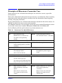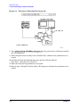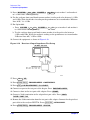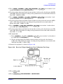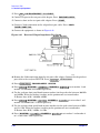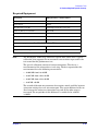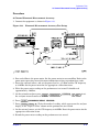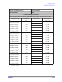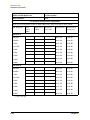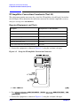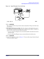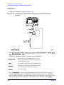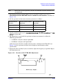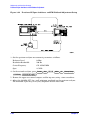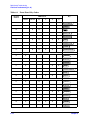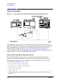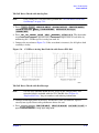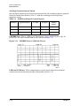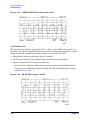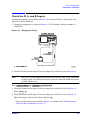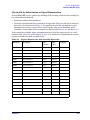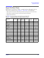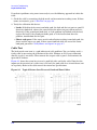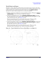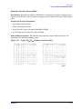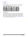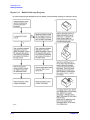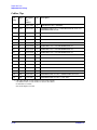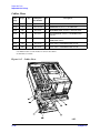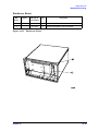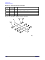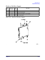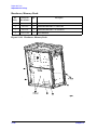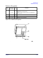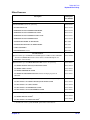
1
Service Guide 8753ES Option 011 Agilent Technologies Network Analyzer Part Number 08753-90485 Printed in USA June 2004 Supersedes Print Date: June 2002 Agilent Technologies, Inc. 1999–2002, 2004 WARRANTY STATEMENT THE MATERIAL CONTAINED IN THIS DOCUMENT IS PROVIDED “AS IS,” AND IS SUBJECT TO BEING CHANGED, WITHOUT NOTICE, IN FUTURE EDITIONS. FURTHER, TO THE MAXIMUM EXTENT PERMITTED BY APPLICABLE LAW, AGILENT DISCLAIMS ALL WARRANTIES, EITHER EXPRESS OR IMPLIED WITH REGARD TO THIS MANUAL AND ANY INFORMATION CONTAINED HEREIN, INCLUDING BUT NOT LIMITED TO THE IMPLIED WARRANTIES OF MERCHANTABILITY AND FITNESS FOR A PARTICULAR PURPOSE. AGILENT SHALL NOT BE LIABLE FOR ERRORS OR FOR INCIDENTAL OR CONSEQUENTIAL DAMAGES IN CONNECTION WITH THE FURNISHING, USE, OR PERFORMANCE OF THIS DOCUMENT OR ANY INFORMATION CONTAINED HEREIN. SHOULD AGILENT AND THE USER HAVE A SEPARATE WRITTEN AGREEMENT WITH WARRANTY TERMS COVERING THE MATERIAL IN THIS DOCUMENT THAT CONFLICT WITH THESE TERMS, THE WARRANTY TERMS IN THE SEPARATE AGREEMENT WILL CONTROL. DFARS/Restricted Rights Notice If software is for use in the performance of a U.S. Government prime contract or subcontract, Software is delivered and licensed as “Commercial computer software” as defined in DFAR 252.227-7014 (June 1995), or as a “commercial item” as defined in FAR 2.101(a) or as “Restricted computer software” as defined in FAR 52.227-19 (June 1987) or any equivalent agency regulation or contract clause. Use, duplication or disclosure of Software is subject to Agilent Technologies’ standard commercial license terms, and non-DOD Departments and Agencies of the U.S. Government will receive no greater than Restricted Rights as defined in FAR 52.227-19(c)(1-2) (June 1987). U.S. Government users will receive no greater than Limited Rights as defined in FAR 52.227-14 (June 1987) or DFAR 252.227-7015 (b)(2) (November 1995), as applicable in any technical data. Certification Agilent Technologies, Inc. certifies that this product met its published specifications at the time of shipment from the factory. Agilent Technologies, Inc. further certifies that its calibration measurements are traceable to the United States National Institute of Standards and Technology, to the extent allowed by the Institute's calibration facility, and to the calibration facilities of other International Standards Organization members. ii Assistance Product maintenance agreements and other customer assistance agreements are available for Agilent Technologies, Inc. products. For information about these agreements and for other assistance, contact Agilent. Refer to “Assistance” on page 15-2. Safety and Regulatory Information The safety and regulatory information pertaining to this product is located in Chapter 15 , “Safety and Regulatory Information.” Safety Notes The following safety notes are used throughout this manual. Familiarize yourself with each of the notes and its meaning before operating this instrument. All pertinent safety notes for using this product are located in Chapter 15 , “Safety and Regulatory Information.” WARNING Warning denotes a hazard. It calls attention to a procedure which, if not correctly performed or adhered to, could result in injury or loss of life. Do not proceed beyond a warning note until the indicated conditions are fully understood and met. CAUTION Caution denotes a hazard. It calls attention to a procedure that, if not correctly performed or adhered to, could result in damage to or destruction of the instrument. Do not proceed beyond a caution sign until the indicated conditions are fully understood and met. iii Documentation Map The Installation and Quick Start Guide provides procedures for installing, configuring, and verifying the operation of the analyzer. It also will help you familiarize yourself with the basic operation of the analyzer. The User’s Guide shows how to make measurements, explains commonly-used features, and tells you how to get the most performance from your analyzer. The Reference Guide provides reference information, such as specifications, menu maps, and key definitions. The Programmer’s Guide provides general GPIB programming information, a command reference, and example programs. The Programmer’s Guide contains a CD-ROM with example programs. The CD-ROM provides the Installation and Quick Start Guide, the User’s Guide, the Reference Guide, and the Programmer’s Guide in PDF format for viewing or printing from a PC. The Service Guide provides information on calibrating, troubleshooting, and servicing your analyzer. The Service Guide is not part of a standard shipment and is available only as Option 0BW. A CD-ROM with the Service Guide in PDF format is included for viewing or printing from a PC. How to Use This Guide This guide uses the following conventions: Front Panel Key This represents a key physically located on the instrument. SOFTKEY This represents a “softkey”, a key whose label is determined by the instrument firmware. Computer Font This represents text displayed on the instrument’s screen, text on a computer display, or a programming command. iv Contents 1. Service Equipment and Analyzer Options Required Tools and Equipment . . . . . . . . . . . . . . . . . . . . . . . . . . . . . . . . . . . . . . . . . . . . . . . . .1-2 Principles of Microwave Connector Care . . . . . . . . . . . . . . . . . . . . . . . . . . . . . . . . . . . . . . . . .1-5 Analyzer Options Available . . . . . . . . . . . . . . . . . . . . . . . . . . . . . . . . . . . . . . . . . . . . . . . . . . . .1-6 Service and Support Options . . . . . . . . . . . . . . . . . . . . . . . . . . . . . . . . . . . . . . . . . . . . . . . . . . .1-7 2. Performance Tests Introduction . . . . . . . . . . . . . . . . . . . . . . . . . . . . . . . . . . . . . . . . . . . . . . . . . . . . . . . . . . . . . . . .2-2 1. Source Frequency Range and Accuracy . . . . . . . . . . . . . . . . . . . . . . . . . . . . . . . . . . . . . . . .2-4 2. Source Power Range, Linearity, and Accuracy . . . . . . . . . . . . . . . . . . . . . . . . . . . . . . . . . .2-6 3. Receiver Minimum R Channel Level . . . . . . . . . . . . . . . . . . . . . . . . . . . . . . . . . . . . . . . . .2-12 4. External Source Mode Frequency Range . . . . . . . . . . . . . . . . . . . . . . . . . . . . . . . . . . . . . .2-14 5. Receiver Channel Noise Floor Level (Only for Analyzers without Option 006) . . . . . . . . . . . . . . . . . . . . . . . . . . . . . . . . . . . . . . . .2-16 6. Receiver Channel Noise Floor Level (Only for Analyzers with Option 006) . . . . . . . . . . . . . . . . . . . . . . . . . . . . . . . . . . . . . . . . . .2-19 7. Receiver Magnitude Frequency Response . . . . . . . . . . . . . . . . . . . . . . . . . . . . . . . . . . . . .2-23 8. Receiver Phase Frequency Response (Ratio) . . . . . . . . . . . . . . . . . . . . . . . . . . . . . . . . . . .2-27 9. Receiver Input Crosstalk . . . . . . . . . . . . . . . . . . . . . . . . . . . . . . . . . . . . . . . . . . . . . . . . . .2-32 10. Receiver Trace Noise . . . . . . . . . . . . . . . . . . . . . . . . . . . . . . . . . . . . . . . . . . . . . . . . . . . . .2-38 11. Receiver Input Impedance . . . . . . . . . . . . . . . . . . . . . . . . . . . . . . . . . . . . . . . . . . . . . . . . .2-42 12. Receiver Magnitude Dynamic Accuracy . . . . . . . . . . . . . . . . . . . . . . . . . . . . . . . . . . . . . .2-48 13. Receiver Magnitude Compression . . . . . . . . . . . . . . . . . . . . . . . . . . . . . . . . . . . . . . . . . . .2-58 14. Receiver Phase Compression . . . . . . . . . . . . . . . . . . . . . . . . . . . . . . . . . . . . . . . . . . . . . . .2-62 15. Source and Receiver Harmonics (Option 002 Only) . . . . . . . . . . . . . . . . . . . . . . . . . . . .2-66 16. Harmonic Measurement Accuracy (Option 002 Only) . . . . . . . . . . . . . . . . . . . . . . . . . . . . . . . . . . . . . . . . . . . . . . . . . . . . . . . . . .2-70 Performance Test Records . . . . . . . . . . . . . . . . . . . . . . . . . . . . . . . . . . . . . . . . . . . . . . . . . . . .2-73 3. Adjustments and Correction Constants Post-Repair Procedures . . . . . . . . . . . . . . . . . . . . . . . . . . . . . . . . . . . . . . . . . . . . . . . . . . . . . . .3-3 A9 Switch Positions . . . . . . . . . . . . . . . . . . . . . . . . . . . . . . . . . . . . . . . . . . . . . . . . . . . . . . . . . .3-6 Source Default Correction Constants (Test 44) . . . . . . . . . . . . . . . . . . . . . . . . . . . . . . . . . . . .3-7 Source Pretune Default Correction Constants (Test 45) . . . . . . . . . . . . . . . . . . . . . . . . . . . . .3-8 Analog Bus Correction Constants (Test 46) . . . . . . . . . . . . . . . . . . . . . . . . . . . . . . . . . . . . . . .3-9 Source Pretune Correction Constants (Test 48) . . . . . . . . . . . . . . . . . . . . . . . . . . . . . . . . . . .3-10 RF Output Power Correction Constants (Test 47) . . . . . . . . . . . . . . . . . . . . . . . . . . . . . . . . .3-11 IF Amplifier Correction Constants (Test 51) . . . . . . . . . . . . . . . . . . . . . . . . . . . . . . . . . . . . .3-16 ADC Offset Correction Constants (Test 52) . . . . . . . . . . . . . . . . . . . . . . . . . . . . . . . . . . . . . .3-18 Sampler Magnitude and Phase Correction Constants (Test 53) . . . . . . . . . . . . . . . . . . . . . . . . . . . . . . . . . . . . . . . . . . . . . . . . . . . . . . . . . . . . . . . . . .3-19 Cavity Oscillator Frequency Correction Constants (Test 54) . . . . . . . . . . . . . . . . . . . . . . . .3-25 Serial Number Correction Constants (Test 55) . . . . . . . . . . . . . . . . . . . . . . . . . . . . . . . . . . .3-30 Option Numbers Correction Constants (Test 56) . . . . . . . . . . . . . . . . . . . . . . . . . . . . . . . . . .3-31 Initialize EEPROMs (Test 58) . . . . . . . . . . . . . . . . . . . . . . . . . . . . . . . . . . . . . . . . . . . . . . . . .3-32 EEPROM Backup Disk Procedure . . . . . . . . . . . . . . . . . . . . . . . . . . . . . . . . . . . . . . . . . . . . .3-33 Correction Constants Retrieval Procedure . . . . . . . . . . . . . . . . . . . . . . . . . . . . . . . . . . . . . . .3-34 Loading Firmware . . . . . . . . . . . . . . . . . . . . . . . . . . . . . . . . . . . . . . . . . . . . . . . . . . . . . . . . . .3-35 Contents-1 Contents Fractional-N Frequency Range Adjustment . . . . . . . . . . . . . . . . . . . . . . . . . . . . . . . . . . . . . 3-39 Frequency Accuracy Adjustment . . . . . . . . . . . . . . . . . . . . . . . . . . . . . . . . . . . . . . . . . . . . . . 3-42 High/Low Band Transition Adjustment . . . . . . . . . . . . . . . . . . . . . . . . . . . . . . . . . . . . . . . . . 3-45 Fractional-N Spur Avoidance and FM Sideband Adjustment . . . . . . . . . . . . . . . . . . . . . . . 3-47 Source Spur Avoidance Tracking Adjustment . . . . . . . . . . . . . . . . . . . . . . . . . . . . . . . . . . . . 3-50 Unprotected Hardware Option Numbers Correction Constants . . . . . . . . . . . . . . . . . . . . . 3-52 Sequences for Mechanical Adjustments . . . . . . . . . . . . . . . . . . . . . . . . . . . . . . . . . . . . . . . . . 3-53 4. Start Troubleshooting Here Start Troubleshooting Here . . . . . . . . . . . . . . . . . . . . . . . . . . . . . . . . . . . . . . . . . . . . . . . . . . . 4-2 Assembly Replacement Sequence . . . . . . . . . . . . . . . . . . . . . . . . . . . . . . . . . . . . . . . . . . . . . . 4-3 Having Your Analyzer Serviced . . . . . . . . . . . . . . . . . . . . . . . . . . . . . . . . . . . . . . . . . . . . . . . . 4-4 Step 1. Initial Observations . . . . . . . . . . . . . . . . . . . . . . . . . . . . . . . . . . . . . . . . . . . . . . . . . . . 4-5 Step 2. Operator's Check . . . . . . . . . . . . . . . . . . . . . . . . . . . . . . . . . . . . . . . . . . . . . . . . . . . . . 4-6 Step 3. GPIB Systems Check . . . . . . . . . . . . . . . . . . . . . . . . . . . . . . . . . . . . . . . . . . . . . . . . . . 4-8 Step 4. Faulty Group Isolation . . . . . . . . . . . . . . . . . . . . . . . . . . . . . . . . . . . . . . . . . . . . . . . . 4-10 Power Supply . . . . . . . . . . . . . . . . . . . . . . . . . . . . . . . . . . . . . . . . . . . . . . . . . . . . . . . . . . . . . 4-11 Digital Control . . . . . . . . . . . . . . . . . . . . . . . . . . . . . . . . . . . . . . . . . . . . . . . . . . . . . . . . . . . . 4-12 Source . . . . . . . . . . . . . . . . . . . . . . . . . . . . . . . . . . . . . . . . . . . . . . . . . . . . . . . . . . . . . . . . . . . 4-14 Receiver . . . . . . . . . . . . . . . . . . . . . . . . . . . . . . . . . . . . . . . . . . . . . . . . . . . . . . . . . . . . . . . . . . 4-17 Accessories . . . . . . . . . . . . . . . . . . . . . . . . . . . . . . . . . . . . . . . . . . . . . . . . . . . . . . . . . . . . . . . 4-19 5. Power Supply Troubleshooting Power Supply Troubleshooting . . . . . . . . . . . . . . . . . . . . . . . . . . . . . . . . . . . . . . . . . . . . . . . . 5-2 Assembly Replacement Sequence . . . . . . . . . . . . . . . . . . . . . . . . . . . . . . . . . . . . . . . . . . . . . . 5-3 Simplified Block Diagram . . . . . . . . . . . . . . . . . . . . . . . . . . . . . . . . . . . . . . . . . . . . . . . . . . . . 5-4 Start Here . . . . . . . . . . . . . . . . . . . . . . . . . . . . . . . . . . . . . . . . . . . . . . . . . . . . . . . . . . . . . . . . . 5-5 If the Green LED of the A15 Is Not ON Steadily . . . . . . . . . . . . . . . . . . . . . . . . . . . . . . . . . . 5-7 If the Red LED of the A15 Is ON . . . . . . . . . . . . . . . . . . . . . . . . . . . . . . . . . . . . . . . . . . . . . . . 5-8 If the Green LEDs of the A8 Are Not All ON . . . . . . . . . . . . . . . . . . . . . . . . . . . . . . . . . . . . 5-13 Error Messages . . . . . . . . . . . . . . . . . . . . . . . . . . . . . . . . . . . . . . . . . . . . . . . . . . . . . . . . . . . . 5-17 Fan Troubleshooting . . . . . . . . . . . . . . . . . . . . . . . . . . . . . . . . . . . . . . . . . . . . . . . . . . . . . . . . 5-19 Intermittent Problems . . . . . . . . . . . . . . . . . . . . . . . . . . . . . . . . . . . . . . . . . . . . . . . . . . . . . . 5-20 6. Digital Control Troubleshooting Digital Control Troubleshooting . . . . . . . . . . . . . . . . . . . . . . . . . . . . . . . . . . . . . . . . . . . . . . . 6-2 Digital Control Group Block Diagram . . . . . . . . . . . . . . . . . . . . . . . . . . . . . . . . . . . . . . . . . . . 6-3 Assembly Replacement Sequence . . . . . . . . . . . . . . . . . . . . . . . . . . . . . . . . . . . . . . . . . . . . . . 6-4 CPU Troubleshooting (A9) . . . . . . . . . . . . . . . . . . . . . . . . . . . . . . . . . . . . . . . . . . . . . . . . . . . . 6-5 Display Troubleshooting (A2, A18, A19, A27) . . . . . . . . . . . . . . . . . . . . . . . . . . . . . . . . . . . . . 6-7 Front Panel Troubleshooting (A1, A2) . . . . . . . . . . . . . . . . . . . . . . . . . . . . . . . . . . . . . . . . . . 6-12 Run the Internal Diagnostic Tests . . . . . . . . . . . . . . . . . . . . . . . . . . . . . . . . . . . . . . . . . . . . . 6-16 If the Fault Is Intermittent . . . . . . . . . . . . . . . . . . . . . . . . . . . . . . . . . . . . . . . . . . . . . . . . . . 6-18 GPIB Failures . . . . . . . . . . . . . . . . . . . . . . . . . . . . . . . . . . . . . . . . . . . . . . . . . . . . . . . . . . . . . 6-19 Contents-2 Contents 7. Source Troubleshooting Source Troubleshooting . . . . . . . . . . . . . . . . . . . . . . . . . . . . . . . . . . . . . . . . . . . . . . . . . . . . . . .7-2 Assembly Replacement Sequence . . . . . . . . . . . . . . . . . . . . . . . . . . . . . . . . . . . . . . . . . . . . . . .7-3 Before You Start Troubleshooting . . . . . . . . . . . . . . . . . . . . . . . . . . . . . . . . . . . . . . . . . . . . . .7-4 Power . . . . . . . . . . . . . . . . . . . . . . . . . . . . . . . . . . . . . . . . . . . . . . . . . . . . . . . . . . . . . . . . . . . . .7-5 Phase Lock Error . . . . . . . . . . . . . . . . . . . . . . . . . . . . . . . . . . . . . . . . . . . . . . . . . . . . . . . . . . . .7-6 Source Group Troubleshooting Appendix . . . . . . . . . . . . . . . . . . . . . . . . . . . . . . . . . . . . . . .7-30 8. Receiver Troubleshooting Receiver Troubleshooting . . . . . . . . . . . . . . . . . . . . . . . . . . . . . . . . . . . . . . . . . . . . . . . . . . . . .8-2 Assembly Replacement Sequence . . . . . . . . . . . . . . . . . . . . . . . . . . . . . . . . . . . . . . . . . . . . . . .8-3 Receiver Failure Error Messages. . . . . . . . . . . . . . . . . . . . . . . . . . . . . . . . . . . . . . . . . . . . . . . .8-4 Check the R, A, and B Inputs . . . . . . . . . . . . . . . . . . . . . . . . . . . . . . . . . . . . . . . . . . . . . . . . . .8-5 Troubleshooting When All Inputs Look Bad . . . . . . . . . . . . . . . . . . . . . . . . . . . . . . . . . . . . . .8-7 Check the 4 MHz REF Signal . . . . . . . . . . . . . . . . . . . . . . . . . . . . . . . . . . . . . . . . . . . . . . . . . .8-8 Troubleshooting When One or More Inputs Look Good . . . . . . . . . . . . . . . . . . . . . . . . . . . .8-11 9. Accessories Troubleshooting Accessories Troubleshooting . . . . . . . . . . . . . . . . . . . . . . . . . . . . . . . . . . . . . . . . . . . . . . . . . . .9-2 Assembly Replacement Sequence . . . . . . . . . . . . . . . . . . . . . . . . . . . . . . . . . . . . . . . . . . . . . . .9-3 Inspect the Accessories . . . . . . . . . . . . . . . . . . . . . . . . . . . . . . . . . . . . . . . . . . . . . . . . . . . . . . .9-4 Inspect the Error Terms . . . . . . . . . . . . . . . . . . . . . . . . . . . . . . . . . . . . . . . . . . . . . . . . . . . . . .9-5 Test Set Troubleshooting . . . . . . . . . . . . . . . . . . . . . . . . . . . . . . . . . . . . . . . . . . . . . . . . . . . . . .9-8 10. Service Key Menus and Error Messages Service Key Menus . . . . . . . . . . . . . . . . . . . . . . . . . . . . . . . . . . . . . . . . . . . . . . . . . . . . . . . . . .10-3 GPIB Service Mnemonic Definitions . . . . . . . . . . . . . . . . . . . . . . . . . . . . . . . . . . . . . . . . . .10-42 Error Messages . . . . . . . . . . . . . . . . . . . . . . . . . . . . . . . . . . . . . . . . . . . . . . . . . . . . . . . . . . .10-44 11. Error Terms Error Terms . . . . . . . . . . . . . . . . . . . . . . . . . . . . . . . . . . . . . . . . . . . . . . . . . . . . . . . . . . . . . . .11-2 Error Terms Can Serve a Diagnostic Purpose . . . . . . . . . . . . . . . . . . . . . . . . . . . . . . . . . . . .11-3 Full Two-Port Error-Correction Procedure . . . . . . . . . . . . . . . . . . . . . . . . . . . . . . . . . . . . . . .11-4 12. Theory of Operation How the Analyzer Works . . . . . . . . . . . . . . . . . . . . . . . . . . . . . . . . . . . . . . . . . . . . . . . . . . . .12-3 A Close Look at the Analyzer's Functional Groups . . . . . . . . . . . . . . . . . . . . . . . . . . . . . . . .12-5 Power Supply Theory . . . . . . . . . . . . . . . . . . . . . . . . . . . . . . . . . . . . . . . . . . . . . . . . . . . . . . .12-6 Digital Control Theory . . . . . . . . . . . . . . . . . . . . . . . . . . . . . . . . . . . . . . . . . . . . . . . . . . . . . .12-9 Source Theory Overview . . . . . . . . . . . . . . . . . . . . . . . . . . . . . . . . . . . . . . . . . . . . . . . . . . . .12-14 Source Super Low Band Operation . . . . . . . . . . . . . . . . . . . . . . . . . . . . . . . . . . . . . . . . . . .12-16 Source Low Band Operation . . . . . . . . . . . . . . . . . . . . . . . . . . . . . . . . . . . . . . . . . . . . . . . . .12-17 Source High Band Operation . . . . . . . . . . . . . . . . . . . . . . . . . . . . . . . . . . . . . . . . . . . . . . . .12-19 Source Operation in Other Modes/Features . . . . . . . . . . . . . . . . . . . . . . . . . . . . . . . . . . . .12-22 Signal Separation . . . . . . . . . . . . . . . . . . . . . . . . . . . . . . . . . . . . . . . . . . . . . . . . . . . . . . . . . .12-26 Receiver Theory . . . . . . . . . . . . . . . . . . . . . . . . . . . . . . . . . . . . . . . . . . . . . . . . . . . . . . . . . . .12-28 Contents-3 Contents 13. Replaceable Parts Replaceable Parts . . . . . . . . . . . . . . . . . . . . . . . . . . . . . . . . . . . . . . . . . . . . . . . . . . . . . . . . . . 13-2 Replacing an Assembly . . . . . . . . . . . . . . . . . . . . . . . . . . . . . . . . . . . . . . . . . . . . . . . . . . . . . . 13-3 Rebuilt-Exchange Assemblies . . . . . . . . . . . . . . . . . . . . . . . . . . . . . . . . . . . . . . . . . . . . . . . . 13-4 Ordering Information . . . . . . . . . . . . . . . . . . . . . . . . . . . . . . . . . . . . . . . . . . . . . . . . . . . . . . . 13-5 Replaceable Part Listings . . . . . . . . . . . . . . . . . . . . . . . . . . . . . . . . . . . . . . . . . . . . . . . . . . . 13-7 14. Assembly Replacement and Post-Repair Procedures Replacing an Assembly . . . . . . . . . . . . . . . . . . . . . . . . . . . . . . . . . . . . . . . . . . . . . . . . . . . . . . 14-3 Line Fuse . . . . . . . . . . . . . . . . . . . . . . . . . . . . . . . . . . . . . . . . . . . . . . . . . . . . . . . . . . . . . . . . . 14-5 Covers . . . . . . . . . . . . . . . . . . . . . . . . . . . . . . . . . . . . . . . . . . . . . . . . . . . . . . . . . . . . . . . . . . . 14-6 Front Panel Assembly . . . . . . . . . . . . . . . . . . . . . . . . . . . . . . . . . . . . . . . . . . . . . . . . . . . . . . 14-8 Front Panel Keyboard and Interface Assemblies (A1, A2) . . . . . . . . . . . . . . . . . . . . . . . . . 14-10 Display, Display Lamp and Inverter Assemblies (A18, A27). . . . . . . . . . . . . . . . . . . . . . . . . . . . . . . . . . . . . . . . . . . . . . . . . . . . . . . . . . . . . . . . 14-12 Rear Panel Assembly. . . . . . . . . . . . . . . . . . . . . . . . . . . . . . . . . . . . . . . . . . . . . . . . . . . . . . . 14-14 Rear Panel Interface Board Assembly (A16) . . . . . . . . . . . . . . . . . . . . . . . . . . . . . . . . . . . . 14-16 Type-N Connector Assembly . . . . . . . . . . . . . . . . . . . . . . . . . . . . . . . . . . . . . . . . . . . . . . . . 14-18 A3 Source Assembly . . . . . . . . . . . . . . . . . . . . . . . . . . . . . . . . . . . . . . . . . . . . . . . . . . . . . . . 14-20 A4, A5, A6 Samplers and A7 Pulse Generator . . . . . . . . . . . . . . . . . . . . . . . . . . . . . . . . . . 14-22 A8, A10, A11, A12, A13, A14 Card Cage Boards . . . . . . . . . . . . . . . . . . . . . . . . . . . . . . . . 14-24 A9 CPU Board . . . . . . . . . . . . . . . . . . . . . . . . . . . . . . . . . . . . . . . . . . . . . . . . . . . . . . . . . . . . 14-26 A9BT1 Battery . . . . . . . . . . . . . . . . . . . . . . . . . . . . . . . . . . . . . . . . . . . . . . . . . . . . . . . . . . . 14-28 A15 Preregulator . . . . . . . . . . . . . . . . . . . . . . . . . . . . . . . . . . . . . . . . . . . . . . . . . . . . . . . . . 14-30 A17 Motherboard Assembly . . . . . . . . . . . . . . . . . . . . . . . . . . . . . . . . . . . . . . . . . . . . . . . . . 14-32 A19 Graphics Processor . . . . . . . . . . . . . . . . . . . . . . . . . . . . . . . . . . . . . . . . . . . . . . . . . . . . 14-35 A20 Disk Drive Assembly . . . . . . . . . . . . . . . . . . . . . . . . . . . . . . . . . . . . . . . . . . . . . . . . . . . 14-36 High Stability Frequency Reference (Option 1D5) Assembly . . . . . . . . . . . . . . . . . . . . . . 14-40 B1 Fan Assembly . . . . . . . . . . . . . . . . . . . . . . . . . . . . . . . . . . . . . . . . . . . . . . . . . . . . . . . . . 14-42 Post-Repair Procedures . . . . . . . . . . . . . . . . . . . . . . . . . . . . . . . . . . . . . . . . . . . . . . . . . . . . 14-43 15. Safety and Regulatory Information General Information . . . . . . . . . . . . . . . . . . . . . . . . . . . . . . . . . . . . . . . . . . . . . . . . . . . . . . . . 15-2 Instrument Markings . . . . . . . . . . . . . . . . . . . . . . . . . . . . . . . . . . . . . . . . . . . . . . . . . . . . . . . 15-4 Safety Symbols . . . . . . . . . . . . . . . . . . . . . . . . . . . . . . . . . . . . . . . . . . . . . . . . . . . . . . . . . . . . 15-5 Safety Considerations . . . . . . . . . . . . . . . . . . . . . . . . . . . . . . . . . . . . . . . . . . . . . . . . . . . . . . . 15-5 Contents-4 1 Service Equipment and Analyzer Options 1-1 Service Equipment and Analyzer Options Required Tools and Equipment Required Tools and Equipment The following is a list of the tools required to service your analyzer: • T-8, T-10, T-15, T-20, and T-25 TORX screwdrivers • Flat-blade screwdrivers — small, medium, and large • 5/16-inch open-end wrench (for SMA nuts) • 2-mm extended bit Allen wrench • 3/16, 5/16, and 9/16-inch hex nut drivers • 5/16-inch open-end torque wrench (set to 10 in-lb) • 2.5-mm hex-key driver • Non-conductive and non-ferrous adjustment tool • Needle-nose pliers • Tweezers • Antistatic work mat with wrist-strap 1-2 Chapter 1 Service Equipment and Analyzer Options Required Tools and Equipment Table 1-1 Service Test Equipment Required Equipment Critical Specifications Recommended Model or HP/Agilent Part Number Usea Spectrum Analyzer Freq. Accuracy ±7 Hz 8563E A, T Frequency Counter Frequency: 300 kHz–3 GHz (6 GHz for Option 006) 5350B/51B/52B P Synthesized Sweeper Maximum spurious input: <−30 dB Residual FM: <20 kHz 83620A P Oscilloscope Bandwidth: 100 MHz Accuracy: 10% any T Digital Voltmeter Resolution: 10 mV any T 436A/437B/438A, E4418A/B or E4419A/B A, P, T Power Meter (GPIB) Power Sensor Frequency: 300 kHz–3 GHz, 50Ω 8482A A, P, T Power Sensor (for Option 006) Frequency: 3 GHz–6 GHz 8481A A, P, T S-Parameter Test Set Frequency Range: 300 kHz–3 GHz for Option 006: 3 GHz–6 GHz 85046A 85047A P Transmission/Reflection Test Set Frequency Range: 300 kHz–3 GHz Directivity: 30 dB 85044A P Tool Kit No substitute 08753-60023 T Photometer Tektronix J16 T Photometer Probe Tektronix J6503 T Light Occluder Tektronix 016-0305-00 T Printer HP ThinkJet, DeskJet, LaserJet P Floppy Disk one 3.5-inch formatted 1.44 MB any A Calibration Kit 7 mm, 50Ω No substitute 85031B P Calibration Kit Type-N, 50Ω No substitute 85032B P Step Attenuator No substitute 8496A Opt. 003, H18 P Fixed Attenuator Type-N, 3 dB 8491A Opt. 003 P Fixed Attenuator (2) Type-N, 20 dB 8491A Opt. 020 A,P, T Fixed Attenuator Type-N, 10 dB 8491A Opt. 010 A,P Fixed Attenuator Type-N, 30 dB 8491A Opt. 030 A,P RF Cable Set 12-inch, phase-matched 11500B A RF Cable Kit Type-N, 50Ω, phase-matched 11851B A, P RF Cable 24-inch, APC-7, 50 Ω 8120-4779 P Chapter 1 1-3 Service Equipment and Analyzer Options Required Tools and Equipment Table 1-1 Service Test Equipment Required Equipment Critical Specifications Recommended Model or HP/Agilent Part Number Usea RF Cable (3) 24-inch, Type-N, 50 Ω 8120-4781 P RF Cable 50Ω, 7-mm, 24-inch, phase-matched 11857D P GPIB Cable 10833A/B/C/D A, P BNC Cable 8120-1840 A, P Low Pass Filter >50 dB @ 2.96 Hz and passband that includes 800 MHz 9135-0198 A Power Splitter (2), 2-way Type-N 11667A, Option 001 A, P Minimum Loss Pad Type-N, 50Ω to 75Ω 11852B P Adapter APC-7 to Type-N (f) 11524A A Adapter APC-7 to Type-N (m) 11525A P Adapter APC-7 to 3.5 mm (m) 1250-1746 A, P Adapter BNC to Alligator Clip 8120-1292 A Adapter APC-3.5 (f) to Type-N (f) 1250-1745 P Adapter Type-N (m) to SMA (f) 1250-1250 A Adapter Type-N (m) to SMA (m) 1250-1562 A Adapter Type-N (f) to Type-N (f) 1250-1472 A, P Adapter Type-N (m) to Type-N (m) 1250-1475 A, P Adapter Type-N (f) to BNC (m) 1250-0077 P Termination (2) 50W, Type-N (m) Return loss: ≥30 dB 909F, Option 012 P Antistatic Wrist Strap 9300-1367 A, P, T Antistatic Wrist Strap Cord 9300-0980 A, P, T Antistatic Table Mat 9300-0797 A, P, T a. P = Performance Tests, A = Adjustments, T = Troubleshooting 1-4 Chapter 1 Service Equipment and Analyzer Options Principles of Microwave Connector Care Principles of Microwave Connector Care Proper connector care and connection techniques are critical for accurate, repeatable measurements. Refer to the calibration kit documentation for connector care information. Prior to making connections to the network analyzer, carefully review the information about inspecting, cleaning, and gaging connectors. Having good connector care and connection techniques extends the life of these devices. In addition, you obtain the most accurate measurements. For additional connector care instruction, contact the nearest Agilent Technologies sales or service office about course numbers HP/Agilent 85050A+24A and 85050A+24D. See the following table for quick reference tips about connector care. Table 1-2 Connector Care Quick Reference Handling and Storage Do Keep connectors clean Do Not Extend sleeve or connector nut Touch mating-plane surfaces Set connectors contact — end down Use plastic end-caps during storage Visual Inspection Do Inspect all connectors carefully Do Not Use a damaged connector — ever Look for metal particles, scratches, and dents Connector Cleaning Do Try compressed air first Do Not Use isopropyl alcohol Use any abrasives Get liquid into plastic support beads Clean connector threads Gaging Connectors Do Clean and zero the gage before use Do Not Use an out-of-spec connector Use the correct gage type Use correct end of calibration block Gage all connectors before first use Making Connections Do Chapter 1 Align connectors carefully Do Not Apply bending force to connection Make preliminary connection lightly Over tighten preliminary connection Turn only the connector nut Twist or screw any connection Use a torque wrench for final connect Tighten past torque wrench “break” point 1-5 Service Equipment and Analyzer Options Analyzer Options Available Analyzer Options Available Option 1D5, High Stability Frequency Reference This option offers ±0.05 ppm temperature stability from 0 to 60 °C (referenced to 25 °C). Option 002, Harmonic Mode This option provides measurement of second or third harmonics of the test device's fundamental output signal. Frequency and power sweep are supported in this mode. Harmonic frequencies can be measured up to the maximum frequency of the receiver. However, the fundamental frequency may not be lower than 16 MHz. Option 006, 6 GHz Operation This option extends the maximum source and receiver frequency of the analyzer to 6 GHz. Option 010, Time Domain This option displays the time domain response of a network by computing the inverse Fourier transform of the frequency domain response. It shows the response of a test device as a function of time or distance. Displaying the reflection coefficient of a network versus time determines the magnitude and location of each discontinuity. Displaying the transmission coefficient of a network versus time determines the characteristics of individual transmission paths. Time domain operation retains all accuracy inherent with the correction that is active in of such devices as SAW filters, SAW delay lines, RF cables, and RF antennas. Option 1CM, Rack Mount Flange Kit without Handles This option is a rack mount kit containing a pair of flanges and the necessary hardware to mount the instrument, with handles detached, in an equipment rack with 482.6 mm (19 inches) horizontal spacing. Option 1CP, Rack Mount Flange Kit with Handles This option ia a rack mount kit containing a pair of flanges and the necessary hardware to mount the instrument with handles attached in an equipment rack with 482.6 mm (19 inches) spacing. 1-6 Chapter 1 Service Equipment and Analyzer Options Service and Support Options Service and Support Options The analyzer’s standard warranty is a one-year return to Agilent Technologies service warranty. NOTE Chapter 1 There are many other repair and calibration options available from the Agilent Technologies support organization. These options cover a range of service agreements with varying response times. Contact Agilent for additional information on available service agreements for this product. Refer to “Contacting Agilent” on page 15-3. 1-7 Service Equipment and Analyzer Options Service and Support Options 1-8 Chapter 1 2 Performance Tests 2-1 Performance Tests Introduction Introduction The performance of the analyzer is verified by confirming that the analyzer’s output and input behavior meets the instrument specifications. The instrument specifications are found in the chapter titled “Specifications and Characteristics” in the analyzer’s reference guide. The section on instrument specifications is divided into two parts: • Source Specifications • Receiver Specifications The performance tests documented in this chapter are used to test the analyzer’s performance against the instrument specifications. If the analyzer passes the performance tests, it meets the instrument specifications. Following is the list of performance tests. 1. Source Frequency Range and Accuracy on page 2-4 2. Source Power Range, Linearity, and Accuracy on page 2-6 3. Receiver Minimum R Channel Level on page 2-12 4. External Source Mode Frequency Range on page 2-14 5. Receiver Channel Noise Floor Level (Only for Analyzers without Option 006) on page 2-16 6. Receiver Channel Noise Floor Level (Only for Analyzers with Option 006) on page 2-19 7. Receiver Magnitude Frequency Response on page 2-23 8. Receiver Phase Frequency Response (Ratio) on page 2-27 9. Receiver Input Crosstalk on page 2-32 10. Receiver Trace Noise on page 2-38 11. Receiver Input Impedance on page 2-42 12. Receiver Magnitude Dynamic Accuracy on page 2-48 13. Receiver Magnitude Compression on page 2-58 14. Receiver Phase Compression on page 2-62 15. Source and Receiver Harmonics (Option 002 Only) on page 2-66 16. Harmonic Measurement Accuracy (Option 002 Only) on page 2-70 2-2 Chapter 2 Performance Tests Introduction Performance Test Records Performance test records for each of the performance tests can be found at the end of this chapter. It is recommended that you use photocopies of the test records to record test results on. Certificate of Calibration Agilent Technologies will issue a Certificate of Calibration for the product upon successful completion of the performance tests. The equipment and measurement standards used for the test must be certified and must be traceable to recognized standards. NOTE Chapter 2 If you have a measurement application that does not use all of the measurement capabilities of the analyzer, you may ask your local Agilent Technologies service center to verify only a subset of the specifications. However, this creates the possibility of making inaccurate measurements if you then use the analyzer in an application requiring additional capabilities. 2-3 Performance Tests 1. Source Frequency Range and Accuracy 1. Source Frequency Range and Accuracy Perform this test to verify the frequency accuracy of the analyzer over its entire operating frequency range. A frequency counter is used to determine the analyzer’s output frequency. Analyzer warm-up time: 30 minutes Specifications Frequency Range Frequency Accuracya 300 kHz to 3 GHz ±10 ppm 30 kHz to 6 GHzb ±10 ppm a. At 25 °C ±5 °C. b. Only for analyzers with Option 006. Required Equipment Description HP/Agilent Part or Model Number Frequency Counter 5350B/51B/52B RF cable set, 50Ω type-N 11851B 2-way power splitter, 50Ω 11667A Option 001 Adapter, type-N (f) to BNC (m) 1250-0077 Procedure 1. Connect the equipment as shown in Figure 2-1. 2-4 Chapter 2 Performance Tests 1. Source Frequency Range and Accuracy Figure 2-1 Source Frequency Range and Accuracy Test Setup 2. Press Preset Sweep Setup CW FREQ . 3. Press 300 k/m (or 30 k/m if the analyzer has Option 006) and write the frequency counter reading on the performance test record. 4. Repeat step 3 for each frequency listed in the performance test record. In Case of Difficulty 1. If any measured frequency is close to the specification limits, check the time base accuracy of the counter used. 2. If the analyzer fails by a significant margin at all frequencies (especially if the deviation increases with frequency), the master time-base probably needs adjustment. In this case, refer to “Frequency Accuracy Adjustment” on page 3-42. The “Fractional-N Frequency Range Adjustment” on page 3-39 can also affect the frequency accuracy. 3. Refer to Chapter 7 , “Source Troubleshooting,” for related troubleshooting information. Chapter 2 2-5 Performance Tests 2. Source Power Range, Linearity, and Accuracy 2. Source Power Range, Linearity, and Accuracy Perform this test to verify the power range and linearity at different CW frequencies throughout the analyzer operating frequency range. Analyzer warm-up time: 30 minutes Specifications Power Range Power Level Accuracya Specification ±1.0 dB Power Level Linearityb −5 to +15 dBm ±0.25 dB +15 to +20 dBm ±0.5 dB Option 006:c −5 to +13 dBm ±0.25 dB +13 to +18 dBm ±0.5 dB a. At 25 °C ±5 °C, and at +10 dBm output level. b. At 25 °C ±5 °C, relative to +10 dBm output level. c. Only for analyzers with Option 006 (6 GHz frequency extension). Required Equipment Description HP/Agilent Model Number Power Meter 436A/437B/438A or E4418B/4419B Power Sensor 8482A 2-way power splitter (2), 50Ω 11667A Option 001 Attenuator (2), 20 dB 8491A Option 020 RF cable set, 50Ω type-N 11851B Additional Equipment for Option 006 Analyzers Power Sensor 2-6 8481A Chapter 2 Performance Tests 2. Source Power Range, Linearity, and Accuracy Procedure Path Loss Calibration 1. Connect the equipment as shown in Figure 2-2. Figure 2-2 Path Loss Calibration Test Setup (#1) 2. Zero and calibrate the power meter. Also set the power meter for dBm. For more information on how to perform this task, refer to the power meter documentation. 3. Press Preset Power 10 x1 . 4. Press Sweep Setup CW FREQ 300 k/m . Set the power meter calibration factor for this CW frequency (except if you are using an HP/Agilent 436A). 5. Write the power meter reading in the “First Value” column on the performance test record. 6. Repeat steps 4 and 5 for the other CW frequencies listed on the performance test record. 7. Connect the equipment as shown in Figure 2-3. Chapter 2 2-7 Performance Tests 2. Source Power Range, Linearity, and Accuracy Figure 2-3 Path Loss Calibration Test Setup (#2) 8. Press Sweep Setup this CW frequency. CW FREQ 300 k/m . Set the power meter calibration factor for 9. Write the power meter reading in the “Second Value” column on the performance test record. 10.Calculate the path loss through the power splitter with this formula: First Value − Second Value = Path Loss 11.Write the result on the performance test record. 12.Repeat steps 8 through 11 for the other CW frequencies listed on the performance test record. 2-8 Chapter 2 Performance Tests 2. Source Power Range, Linearity, and Accuracy Power Range and Power Linearity 13.Connect the equipment as shown in Figure 2-4. Figure 2-4 Power Range, Linearity, and Accuracy Test Setup 14.Press Preset Sweep Setup factor for this CW frequency. CW FREQ 300 k/m . Set the power meter calibration 15.Press Power 10 x1 . On the power meter, set the current power level as the reference for relative power (dB) measurements. This can be done by either pressing dB REL on an HP/Agilent 436A or REL on a 438A power meter front panel. 16.Press Power −5 x1 . Write the power meter reading in the “Measured Value” column on the performance test record. 17.With the power offset value that is listed in the performance test record, calculate the power linearity using this formula: Power Linearity = [Power Offset] + [Measured Value] 18.Write the result of your calculation on the performance test record. 19.Repeat steps 16 through 18 for the other source power levels listed on the performance test record. 20.Press Sweep Setup CW FREQ 3 G/n . 21.Press Power 10 x1 . Set the power meter calibration factor for the selected CW frequency. Press the appropriate hardkey (dB REL or REL) on the 436A/438A power meter front panel for relative power measurements. 22.Press Power −5 x1 . Write the power meter reading in the “Measured Value” column on the performance test record. Chapter 2 2-9 Performance Tests 2. Source Power Range, Linearity, and Accuracy 23.With the power offset value listed in the performance test record, calculate the source power level linearity using this formula: Power Linearity = [Power Offset] + [Measured Value] 24.Write the result of your calculation on the performance test record. 25.Repeat steps 21 through 24 for the other power levels listed on the performance test record. For Analyzers with Option 006 26.Press Sweep Setup CW FREQ 6 G/n . 27.Repeat steps 21 through 24 for the other power levels listed on the performance test record. Power Level Accuracy 28.Press Power 10 29.Press Sweep Setup this CW frequency. x1 . CW FREQ 300 k/m . Set the power meter calibration factor for 30.On the performance test record, copy the “Path Loss” value, previously calculated for this CW frequency, into the “Path Loss” column. 31.Calculate the calibrated source power level using this formula: Calibrated Power Level = 10 − Path Loss 32.Write the result in the “Calibrated Power Level” column. 33.Set the power meter for absolute power measurement. 34.Write the power meter reading under the “Measured Value” column on the performance test record. 35.Calculate the power level accuracy using this formula: Calibrated Power Level − Measured Value = Power level Accuracy 36.Write this value on the performance test record. 37.Repeat steps 29 through 35 for the other CW frequencies listed on the performance test record. 2-10 Chapter 2 Performance Tests 2. Source Power Range, Linearity, and Accuracy In Case of Difficulty 1. Ensure that the power meter and power sensor are operating to specification. 2. Inspect the power splitter connectors. Poor match at these connections can generate power reflections that can cause the analyzer to appear to be out of specification. 3. Inspect the analyzer RF OUT connector for damage. 4. If any test fails, perform “RF Output Power Correction Constants (Test 47)” on page 3-11. 5. For a source failure, refer to Chapter 7 , “Source Troubleshooting,” for troubleshooting information. Chapter 2 2-11 Performance Tests 3. Receiver Minimum R Channel Level 3. Receiver Minimum R Channel Level Perform this test to verify the minimum R channel input power level at which phase lock can be accomplished. Analyzer warmup time: 30 minutes. Specifications Frequency Range Minimum R Channel Level 300 kHz–3 GHz −35 dBm 3 GHz–6 GHza −30 dBm a. Only for analyzers with Option 006. Required Equipment Description HP/Agilent Part or Model Number Cable Type-N (m) to Type-N (m) 24-inch 11500B Attenuator, 30 dB 8491A Option 030 Procedure 1. Connect the equipment as shown in Figure 2-5. Figure 2-5 2-12 Receiver Minimum R Channel Level Test Setup Chapter 2 Performance Tests 3. Receiver Minimum R Channel Level 2. Press Preset R. Meas 3. Press Marker Search TRACKING ON SEARCH:MAX to locate the maximum value of the R channel input signal. 4. Press Power −10 5. Press Sweep Setup x1 . CW FREQ 300 k/m . 6. Check the analyzer display for phase lock error messages: • If you do not observe a phase lock error message, write the marker value readout (which appears in the analyzer display) in the performance test record. • If you do observe a phase lock error message: a. Press Power to increase the power by 1 dBm. b. Check the analyzer for phase lock error messages. c. If the analyzer still doesn't phase lock, continue increasing the source output power until phase lock is achieved. d. Write the marker value in the performance test record. • Repeat steps 5 and 6 for the other CW frequencies listed on the performance test record. In Case of Difficulty 1. Check the flexible RF cable between the R sampler assembly and the A11 phase lock assembly. Make sure it is connected between A11J1 (PL IF IN) and 1st IF Out. 2. Use an ohmmeter to verify that the RF cable is not open. In addition, examine both the cable connectors — measure the resistance between the cable center pin and the cable connector. The ohmmeter should display a high resistance reading. 3. Check the R sampler by substituting it with the A sampler and rerun the test: a. Move cable W8 to the A sampler. b. Use a 10 dB attenuator between the RF OUT and input A. c. Repeat the test. d. Select the A sampler by pressing Meas A in step 2. e. If the test fails, replace the A11 assembly. 4. Verify that the high/low band adjustments are still within specifications. For more information on how to perform this task, refer to “High/Low Band Transition Adjustment” on page 3-45. 5. Refer to Chapter 7 , “Source Troubleshooting,” for troubleshooting information. Chapter 2 2-13 Performance Tests 4. External Source Mode Frequency Range 4. External Source Mode Frequency Range Perform this test to verify proper phase lock for selected test frequencies in the external source mode, at the specified minimum R input level of −25 dBm. Analyzer warmup time: 30 minutes Specifications Frequency Rangea 300 kHz–3 GHz 3 GHz–6 GHzb a. At −25 dBm R input level. b. Only for analyzers with Option 006. Required Equipment Description HP/Agilent Part or Model Number External source 83620A Attenuator, 10 dB 8491A Option 010 Attenuator, 20 dB 8491A Option 020 Cable, 50 Ω type-N 11851B Adapter, APC-3.5 (f) to type-N (f) 1820-1745 Procedure 1. Connect the equipment as shown in Figure 2-6. 2-14 Chapter 2 Performance Tests 4. External Source Mode Frequency Range Figure 2-6 External Source Mode Frequency Range Test Setup 2. Preset the external source, and set the power level to 4 dBm, and the CW frequency to 10 MHz. 3. On the network analyzer, press Preset System INSTRUMENT MODE Sweep Setup CW FREQ 10 M/µ EXT SOURCE AUTO to set up the analyzer for an external source input to the receiver channel R. 4. Press Meas R. 5. Press Marker Search TRACKING ON SEARCH:MAX to observe the maximum value of the receiver R input signal. The analyzer marker 1 reading should be ≤ −25 dBm. If this is not the case, adjust the output power of the external source to achieve this condition. 6. Check to see if the analyzer is phase-locking to the external CW signal. • If the analyzer displays any phase lock error-messages, write “UNLOCK” in the performance test record for the set CW signal. • If the analyzer does not display any phase lock error-messages, write “LOCK” in the performance test record for the set CW signal. 7. On the external source, set the CW frequency to 20 MHz. 8. On the network analyzer, press Sweep Setup CW FREQ 20 M/µ . 9. Repeat steps 7 and 8 for the CW frequencies listed on the performance test record. In Case of Difficulty 1. Check the R sampler assembly by substituting it with the A sampler assembly. 2. Move the flexible RF cable (currently connected to the R sampler assembly) to the A sampler assembly. 3. Use a 10 dB attenuator between the RF OUT and the analyzer receiver input A. 4. Repeat the test. In step 4, press Meas A. 5. If the test still fails, suspect the A11 phase lock board assembly. Chapter 2 2-15 Performance Tests 5. Receiver Channel Noise Floor Level (Only for Analyzers without Option 006) 5. Receiver Channel Noise Floor Level (Only for Analyzers without Option 006) Perform this test to determine the analyzer receiver channel noise floor levels. Analyzer warmup time: 30 minutes. Specifications Frequency Range Receiver Input IF Bandwidth Average Noise Level 300 kHz–3.0 GHz A 3 kHz −90 dBm 300 kHz–3.0 GHz A 10 Hz −110 dBm 300 kHz–3.0 GHz B 3 kHz −90 dBm 300 kHz–3.0 GHz B 10 Hz −110 dBm Required Equipment Description HP/Agilent Part or Model Number Attenuator, 20 dB 8491A Option 020 Termination (2), 50Ω 909F Option 012a Cable, 50Ω type-N 24-inch Part of the 11851B cable set a. Or use the terminations included in the 85032B calibration kit. Procedure 1. Connect the equipment as shown in Figure 2-7. 2-16 Chapter 2 Performance Tests 5. Receiver Channel Noise Floor Level (Only for Analyzers without Option 006) Figure 2-7 Receiver Channel Noise Floor Level Test Setup 2. Press Preset −10 Power x1 . Receiver Channel A Noise Floor Level with 3 kHz IF BW 3. Press Meas A Format 4. Press Marker Fctn TRIGGER MENU LIN MAG Scale Ref MARKER MODE MENU SINGLE . AUTO SCALE . MKR STATS ON Sweep Setup 5. When the analyzer finishes the sweep, notice the mean value, which appears on the analyzer display. 6. Use the following equation to convert the linear magnitude mean value to log magnitude: Power (dBm) = 20 × [log10(linear magnitude mean value)] 7. Write this calculated value in the performance test record in dBm. Receiver Channel A Noise Floor Level with 10 Hz IF BW 8. Press Avg IF BW 9. Press Sweep Setup 10 x1 to change the IF bandwidth to 10 Hz. TRIGGER MENU SINGLE . 10.When the analyzer finishes the sweep, notice the mean value, which appears on the analyzer display. 11.Use the following equation to convert the linear magnitude mean value to log magnitude: Power (dBm) = 20 × [log10(linear magnitude mean value)] 12.Write this calculated value in the performance test record in dBm. Chapter 2 2-17 Performance Tests 5. Receiver Channel Noise Floor Level (Only for Analyzers without Option 006) Receiver Channel B Noise Floor Level with 10 Hz IF BW 13.Press Meas B Format 14.Press Sweep Setup LIN MAG . TRIGGER MENU SINGLE . 15.When the analyzer finishes the sweep, notice the mean value, which appears on the analyzer display. 16.Use the following equation to convert the linear magnitude mean value to log magnitude: Power (dBm) = 20 × [log10(linear magnitude mean value)] 17.Write this calculated value in the performance test record in dBm. Receiver Channel B Noise Floor Level with a 3 kHz IF BW 18.Press Avg IF BW 19.Press Sweep Setup 3 k/m to change the IF bandwidth to 3 kHz. TRIGGER MENU SINGLE . 20.When the analyzer finishes the sweep, record the mean value, which appears on the analyzer display. 21.Use the following equation to convert the linear magnitude mean value to log magnitude: Power (dBm) = 20 × [log10(linear magnitude mean value)] 22.Write this calculated value in the performance test record in dBm. In Case of Difficulty 1. Perform “ADC Offset Correction Constants (Test 52)” on page 3-18. 2. Suspect the A10 digital IF assembly if both receiver channels fail. 3. Refer to Chapter 8 , “Receiver Troubleshooting,” for troubleshooting information. 2-18 Chapter 2 Performance Tests 6. Receiver Channel Noise Floor Level (Only for Analyzers with Option 006) 6. Receiver Channel Noise Floor Level (Only for Analyzers with Option 006) Perform this test to determine the analyzer's receiver channel noise floor levels. Analyzer warmup time: 30 minutes. Specifications Frequency Range Receiver Input IF Bandwidth Average Noise Level 300 kHz–3.0 GHz A 3 kHz −90 dBm 300 kHz–3.0 GHz A 10 Hz −110 dBm 300 kHz–3.0 GHz B 3 kHz −90 dBm 300 kHz–3.0 GHz B 10 Hz −110 dBm 3.0 GHz–6.0 GHz A 3 kHz −85 dBm 3.0 GHz–6.0 GHz A 10 Hz −105 dBm 3.0 GHz–6.0 GHz B 3 kHz −85 dBm 3.0 GHz–6.0 GHz B 10 Hz −105 dBm Required Equipment Description HP/Agilent Part or Model Number Attenuator, 20 dB 8491A Option 020 Termination (2), 50Ω 909F Option 012a Cable, 50Ω type-N, 24-inch Part of the 11851B Cable Set a. Or use the terminations included in the 85032B calibration kit. Procedure 1. Connect the equipment as shown in Figure 2-8. Chapter 2 2-19 Performance Tests 6. Receiver Channel Noise Floor Level (Only for Analyzers with Option 006) Figure 2-8 Receiver Channel Noise Floor Level Test Setup 2. Press Preset Start 50 k/m Stop 3 G/n Power −10 x1 . Channel A Noise Floor Level for 3 kHz IF BW (300 kHz–3 GHz) 3. Press Meas A Format 4. Press Marker Fctn TRIGGER MENU LIN MAG Scale Ref MARKER MODE MENU SINGLE . AUTO SCALE . MKR STATS ON Sweep Setup 5. When the analyzer finishes the sweep, notice the mean value, which appears on the analyzer display. 6. Use the following equation to convert the linear magnitude mean value to log magnitude: Power (dBm) = 20 × [log10(linear magnitude mean value)] 7. Write this calculated value in the performance test record in dBm. Channel A Noise Floor Level for 10 Hz IF BW (300 kHz–3 GHz) 8. Press Avg IF BW 9. Press Sweep Setup 10 x1 to change the IF bandwidth to 10 Hz. TRIGGER MENU SINGLE . 10.When the analyzer finishes the sweep, notice the mean value, which appears on the analyzer display. 11.Use the following equation to convert the linear magnitude mean value to log magnitude: Power (dBm) = 20 × [log10(linear magnitude mean value)] 12.Write this calculated value in the performance test record in dBm. 2-20 Chapter 2 Performance Tests 6. Receiver Channel Noise Floor Level (Only for Analyzers with Option 006) Channel B Noise Floor Level for 10 Hz IF BW (300 kHz–3 GHz) 13.Press Meas B Format 14.Press Sweep Setup LIN MAG . TRIGGER MENU SINGLE . 15.When the analyzer finishes the sweep, notice the mean value, which appears on the analyzer display. 16.Use the following equation to convert the linear magnitude mean value to log magnitude: Power (dBm) = 20 × [log10(linear magnitude mean value)] 17.Write this calculated value in the performance test record in dBm. Channel B Noise Floor Level with 3 kHz IF BW (300 kHz–3 GHz) 18.Press Avg IF BW 19.Press Sweep Setup 3 k/m to change the IF bandwidth to 3 kHz. TRIGGER MENU SINGLE . 20.When the analyzer finishes the sweep, notice the mean value, which appears on the analyzer display. 21.Use the following equation to convert the linear magnitude mean value to log magnitude: Power (dBm) = 20 × [log10(linear magnitude mean value)] 22.Write this calculated value in the performance test record in dBm. Channel B Noise Floor Level with 3 kHz IF BW (3 GHz–6 GHz) 23.Press Start 3 G/n 24.Press Sweep Setup Stop 6 G/n . TRIGGER MENU SINGLE . 25.When the analyzer finishes the sweep, record the mean value which appears on the analyzer display. 26.Use the following equation to convert the linear magnitude mean value to log magnitude: Power (dBm) = 20 × [log10(linear magnitude mean value)] 27.Write this calculated value in the performance test record in dBm. Channel B Noise Floor Level with 10 Hz IF BW (3 GHz–6 GHz) 28.Press Avg IF BW 29.Press Sweep Setup 10 x1 to change the IF bandwidth to 10 Hz. TRIGGER MENU SINGLE . 30.When the analyzer finishes the sweep, write the mean value, which appears on the analyzer display. Chapter 2 2-21 Performance Tests 6. Receiver Channel Noise Floor Level (Only for Analyzers with Option 006) 31.Use the following equation to convert the linear magnitude mean value to log magnitude: Power (dBm) = 20 × [log10(linear magnitude mean value)] 32.Write this calculated value in the performance test record in dBm. Channel A Noise Floor Level with 10 Hz IF BW (3 GHz–6 GHz) 33.Press Meas A. 34.Press Sweep Setup TRIGGER MENU SINGLE . 35.When the analyzer finishes the sweep, record the mean value, which appears on the analyzer display. 36.Use the following equation to convert the linear magnitude mean value to log magnitude: Power (dBm) = 20 × [log10(linear magnitude mean value)] 37.Write this calculated value in the performance test record in dBm. Channel A Noise Floor Level with 3 kHz IF BW (3 GHz–6 GHz) 38.Press Avg IF BW 39.Press Sweep Setup 3 k/m . TRIGGER MENU SINGLE . 40.When the analyzer finishes the sweep, notice the mean value, which appears on the analyzer display. 41.Use the following equation to convert the linear magnitude mean value to log magnitude: Power (dBm) = 20 × [log10(linear magnitude mean value)] 42.Write this calculated value in the performance test record in dBm. In Case of Difficulty 1. Perform “ADC Offset Correction Constants (Test 52)” on page 3-18. 2. Suspect the A10 digital IF assembly if both receiver channels fail. 3. Refer to Chapter 8 , “Receiver Troubleshooting,” for troubleshooting information. 2-22 Chapter 2 Performance Tests 7. Receiver Magnitude Frequency Response 7. Receiver Magnitude Frequency Response Perform this test to verify how well the analyzer transfers information from the RF to IF, and how accurately it processes and displays that information. Analyzer warmup time: 30 minutes. Specifications Frequency Range Magnitude Frequency Responsea 300 kHz–3 GHz ± 1 dB 3 GHz–6 GHzb ± 2 dB a. At 25 °C ± 5 °C; A, B, R, −10 dBm input. b. Only for analyzers with Option 006. Required Equipment Description HP/Agilent Part or Model Number Power Meter 436A/437B/438A or E4418B/4419B Power Sensor 8482A 2-Way power splitter, 50Ω 11667A Option 001 Attenuator, 10 dB 8491A Option 010 RF cable set, 50Ω type-N 11851B Adapter, type-N (m) to type-N (m) 1250-1475 Adapter, type-N (f) to type-N (f) 1250-1472 Additional Equipment for Option 006 Analyzers Power Sensor 8481A Procedure Input R Magnitude Frequency Response 1. Connect the equipment as shown in Figure 2-9. Chapter 2 2-23 Performance Tests 7. Receiver Magnitude Frequency Response Figure 2-9 Magnitude Frequency Response Test Setup (Receiver Input R) 2. Zero and calibrate the power meter. Set it to measure dBm. 3. Press Preset Marker Meas 4. Press Sweep Setup CW FREQ meter for this CW frequency. R Power 300 6 x1 . k/m . Set the calibration factor on the power 5. Write the power meter reading on the performance test record. 6. Write the marker reading, which appears on the analyzer display, in the “R Input Power” column of the performance test record. 7. Repeat steps 4, 5 and 6 for the other CW frequencies listed on the performance test record. Input A Magnitude Frequency Response 8. Connect the equipment as shown in Figure 2-10. 2-24 Chapter 2 Performance Tests 7. Receiver Magnitude Frequency Response Figure 2-10 Magnitude Frequency Response Test Setup (Receiver Input A) 9. Press Meas A 10.Press CW FREQ Sweep Setup 300 to measure the power at the receiver input A channel. k/m . 11.Write the marker reading in the “A Input Power” column on the performance test record. 12.Repeat steps 10 and 11 for the other CW frequencies listed on the performance test record. Input B Magnitude Frequency Response 13.Reconfigure the equipment as shown in Figure 2-11. Figure 2-11 Chapter 2 Magnitude Frequency Response Test Setup (Receiver Input B) 2-25 Performance Tests 7. Receiver Magnitude Frequency Response 14.Press Meas B to start measuring the power delivered to receiver input B. 15.Press Sweep Setup CW FREQ 300 k/m . 16.Write the marker reading in the “B Input Power” column on the performance test record. 17.Repeat steps 15 and 16 for the other CW frequencies listed on the performance test record. 18.For each CW frequency, determine which channel input reading shows the greatest difference: • power meter versus R • power meter versus A • power meter versus B Refer to the first line for an example listed in the performance test record. Write the greatest difference in the space provided on the performance test record. NOTE The final results represent the worst case magnitude frequency response for all the analyzer receiver inputs at the selected frequencies. In Case of Difficulty 1. Suspect poor tracking between the ports of the power splitter if all receiver inputs fail. Try to repeat the test with another power splitter. 2. Suspect source drift if receiver inputs A and B fail this test at any frequency. Connect the equipment as shown in Figure 2-10 (or Figure 2-11); set the analyzer source power at the frequency of interest. Repeat the test for the receiver input(s) that failed before. 3. Perform “Sampler Magnitude and Phase Correction Constants (Test 53)” on page 3-19. Repeat this performance test. 4. Consult Chapter 8 , “Receiver Troubleshooting,” for troubleshooting information. 2-26 Chapter 2 Performance Tests 8. Receiver Phase Frequency Response (Ratio) 8. Receiver Phase Frequency Response (Ratio) Perform this test to determine the phase tracking frequency response for each pair of inputs (A/R, B/R and A/B) in the swept sweep mode. Analyzer warmup time: 30 minutes. Specifications Frequency Range Phase Frequency Responsea, b 300 kHz–3 GHz ± 3° 3 GHz–6 GHzc ± 10° a. Deviation from linear phase. IF BW ≤ 300 Hz and 3 second sweeptime for A/B measurements. b. At 25 °C ± 5 °C, with −10 dBm into all receiver inputs. c. Only for analyzers with Option 006. Required Equipment Description HP/Agilent Part or Model Number 2-way power splitter (2), 50Ω 11667A, Option 001 RF cable set, 50Ω Type-N 11851B RF cable, 50Ω Type-N 8120-4781 50 Ω Termination from 85032B Type-N calibration kit Procedure A/R Phase Frequency Response 1. Connect the equipment as shown in Figure 2-12 with the second type-N cable from the RF cable set connected to port A. Chapter 2 2-27 Performance Tests 8. Receiver Phase Frequency Response (Ratio) Figure 2-12 Phase Frequency Response Test Setup From 300 kHz to 3 GHz 2. Press Preset Start 3. Press Power 3 4. Press Avg 300 x1 IF BW k/m . SWEEP TIME Return 3000 3 x1 . 5. Only For Analyzers with Option 006: Press Stop 6. Press Format PHASE x1 . Marker Fctn 3 G/n . MARKER MODE MENU MKR STATS ON . 7. Press Scale Ref 0.6 x1 ELECTRICAL DELAY . Turn the analyzer front panel knob to vary the electrical delay until the trace is in the most linear horizontal position. 8. Press Sweep Setup TRIGGER MENU SINGLE . Press Marker MARKER 1 Marker Search SEARCH: MAX . Press Marker MARKER 2 Marker Search SEARCH: MIN . Record the marker 1 or marker 2 value—whichever has the greatest absolute value—in the “Measured Value” column of the performance test record. From 3 GHz to 6 GHz (Option 006) 9. Press CONTINUOUS Start 3 G/n Stop 6 G/n . 10.Press Scale Ref 5 x1 ELECTRICAL DELAY . Turn the analyzer front panel knob to vary the electrical delay until the trace is in the most linear horizontal position. 11.Press Sweep Setup TRIGGER MENU SINGLE . Press Marker MARKER 1 MARKER 2 Marker Search Marker Search SEARCH: MAX . Press Marker SEARCH: MIN . Record the marker 1 or marker 2 value—whichever has the greatest absolute value—in the “Measured Value” column of the performance test record. 2-28 Chapter 2 Performance Tests 8. Receiver Phase Frequency Response (Ratio) B/R Phase Frequency Response 12.Connect the second type-N cable from the RF cable set to port B. From 300 kHz to 3 GHz 13.Press CONTINUOUS 14.Press Meas B/R Start Format 300 k/m . PHASE . 15.Only For Analyzers with Option 006: Press Stop 3 G/n . 16.Press Scale Ref 0.6 x1 ELECTRICAL DELAY . Turn the analyzer front panel knob to vary the electrical delay until the trace is in the most linear horizontal position. 17.Press Sweep Setup TRIGGER MENU SINGLE . Press Marker MARKER 1 Marker Search SEARCH: MAX . Press Marker MARKER 2 Marker Search SEARCH: MIN . Record the marker 1 or marker 2 value—whichever has the greatest absolute value—in the “Measured Value” column of the performance test record. From 3 GHz to 6 GHz (Option 006) 18.Press CONTINUOUS Start 3 G/n Stop 6 G/n . 19.Press Scale Ref 5 x1 ELECTRICAL DELAY . Turn the analyzer front panel knob to vary the electrical delay until the trace is in the most linear horizontal position. 20.Press Sweep Setup MARKER 1 TRIGGER MENU Marker Search SINGLE . Press SEARCH: MAX . Press Marker Marker MARKER 2 Marker Search SEARCH: MIN . Record the marker 1 or marker 2 value—whichever has the greatest absolute value—in the “Measured Value” column of the performance test record. A/B Phase Frequency Response 21.Connect the equipment as shown in Figure 2-13. Chapter 2 2-29 Performance Tests 8. Receiver Phase Frequency Response (Ratio) Figure 2-13 Phase Frequency Response Test Setup From 300 kHz to 3 GHz 22.Press CONTINUOUS 23.Press Avg 24.Press Meas Start IF BW 300 A/B Format 300 k/m . x1 . PHASE . 25.Only For Analyzers with Option 006: Press Stop 3 G/n . 26.Press Scale Ref 0.6 x1 ELECTRICAL DELAY . Turn the analyzer front panel knob to vary the electrical delay until the trace is in the most linear horizontal position. 27.Press Sweep Setup TRIGGER MENU SINGLE . Press Marker MARKER 1 Marker Search SEARCH: MAX . Press Marker MARKER 2 Marker Search SEARCH: MIN . Record the marker 1 or marker 2 value—whichever has the greatest absolute value—in the “Measured Value” column of the performance test record. From 3 GHz to 6 GHz (Option 006) 28.Press CONTINUOUS Start 3 G/n Stop 6 G/n . 29.Press Scale Ref 5 x1 ELECTRICAL DELAY . Turn the analyzer front panel knob to vary the electrical delay until the trace is in the most linear horizontal position. 30.Press Sweep Setup TRIGGER MENU SINGLE . Press Marker MARKER 1 Marker Search SEARCH: MAX . Press Marker MARKER 2 Marker Search SEARCH: MIN . Record the marker 1 or marker 2 value—whichever has the greatest absolute value—in the “Measured Value” column of the performance test record. 2-30 Chapter 2 Performance Tests 8. Receiver Phase Frequency Response (Ratio) In Case of Difficulty 1. Verify that the RF cables are in a good condition. Move the RF cables to different ports on the power splitter and re-measure the receiver input(s) that failed. 2. Perform “Sampler Magnitude and Phase Correction Constants (Test 53)” on page 3-19. 3. Consult Chapter 8 , “Receiver Troubleshooting,” for troubleshooting information. Chapter 2 2-31 Performance Tests 9. Receiver Input Crosstalk 9. Receiver Input Crosstalk Perform this test to verify the signal leakage interference between input and output test ports, with one port driven and the other one terminated. Analyzer warmup time: 30 minutes. Specifications Frequency Range Crosstalka 300 kHz–1 GHz −100 dB 1 GHz–3 GHz −90 dB 3 GHz–4.5 GHz −82 dB 4.5–6.0 GHz −75 dB a. At 10 Hz IF Bandwidth Required Equipment Description HP/Agilent Model Number 2-way power splitter (2), 50Ω 11667A Option 001 Termination (3), 50Ω 909F Option 012a Attenuator, 20 dB 8491A Option 020 RF cable set, 50Ω, type-N 11851B a. Or use terminations included in 85032B calibration kits. Procedure R into A Crosstalk from 300 kHz to 1 GHz 1. Connect the equipment as shown in Figure 2-14. 2-32 Chapter 2 Performance Tests 9. Receiver Input Crosstalk Figure 2-14 R into A and R into B Crosstalk Test Setup 2. Press Preset Power AVERAGING ON 3. Press Scale Ref IF BW 1 x1 AVERAGING FACTOR Avg 5 x1 x1 . 10 x1 to get a better scaling of the data trace. 25 4. Press Marker Search 5. Press Stop x1 . 6 SEARCH:MAX . TRACKING ON G/n Sweep Setup TRIGGER MENU NUMBER of GROUPS 5 6. When the analyzer finishes the number of sweeps, write the marker value, which appears on the analyzer display, on the performance test record. R into A Crosstalk from 1 GHz to 3 GHz 7. Press Start 1 G/n Stop 3 G/n NUMBER of GROUPS x1 . 5 8. When the analyzer finishes the number of sweeps, write the marker value, which appears on the analyzer display, on the performance test record. (Only for Option 006 Analyzers) R into A Crosstalk from 3 GHz to 4.5 GHz 9. Press Start 3 G/n Stop 4.5 G/n NUMBER of GROUPS 5 x1 . 10.When the analyzer finishes the number of sweeps, write the marker value, which appears on the analyzer display, on the performance test record. (Only for Option 006 Analyzers) R into A Crosstalk from 4.5 GHz to 6 GHz 11.Press Start 4.5 G/n Stop 6 G/n NUMBER of GROUPS 5 x1 . 12.When the analyzer finishes the number of sweeps, write the marker value, which appears on the analyzer display, on the performance test record. R into B Crosstalk from 300 kHz to 1 GHz 13.Press Start Chapter 2 300 k/m Stop 1 G/n . 2-33 Performance Tests 9. Receiver Input Crosstalk 14.Press Meas x1 . B/R TRIGGER MENU Sweep Setup NUMBER of GROUPS 5 15.When the analyzer finishes the number of sweeps, write the marker value, which appears on the analyzer display, on the performance test record. R into B Crosstalk from 1 GHz to 3 GHz 16.Press Start 5 x1 . 1 G/n Stop 3 G/n TRIGGER MENU NUMBER of GROUPS 17.When the analyzer finishes the number of sweeps, write the marker value, which appears on the analyzer display, on the performance test record. (Only for Option 006 Analyzers) R into B Crosstalk from 3 GHz to 4.5 GHz 18.Press Start 5 x1 . 3 G/n Stop 4.5 G/n TRIGGER MENU NUMBER of GROUPS 19.When the analyzer finishes the number of sweeps, write the marker value, which appears on the analyzer display, on the performance test record. (Only for Option 006 Analyzers) R into B Crosstalk from 4.5 GHz to 6 GHz 20.Press Start 5 x1 . 4.5 G/n Stop 6 G/n TRIGGER MENU NUMBER of GROUPS 21.When the analyzer finishes the number of sweeps, write the marker value, which appears on the analyzer display, on the performance test record. B into A Crosstalk from 300 kHz to 1 GHz 22.Connect the equipment as shown in Figure 2-15. Figure 2-15 23.Press Start 2-34 B into A Receiver Input Crosstalk Test Setup 300 k/m Stop 1 G/n . Chapter 2 Performance Tests 9. Receiver Input Crosstalk 24.Press Meas x1 . A/B TRIGGER MENU Sweep Setup NUMBER of GROUPS 5 25.When the analyzer finishes the number of sweeps, write the marker value, which appears on the analyzer display, on the performance test record. B into A Crosstalk from 1 GHz to 3 GHz 26.Press Start 5 x1 . 1 G/n Stop 3 G/n TRIGGER MENU NUMBER of GROUPS 27.When the analyzer finishes the number of sweeps, write the marker value, which appears on the analyzer display, on the performance test record. (Only for Option 006 Analyzers) B into A Crosstalk from 3 GHz to 4.5 GHz 28.Press Start 5 x1 . 3 G/n Stop 4.5 G/n TRIGGER MENU NUMBER of GROUPS 29.When the analyzer finishes the number of sweeps, write the marker value, which appears on the analyzer display, on the performance test record. (Only for Option 006 Analyzers) B into A Crosstalk from 4.5 GHz to 6 GHz 30.Press Start 5 x1 . 4.5 G/n Stop 6 G/n TRIGGER MENU NUMBER of GROUPS 31.When the analyzer finishes the number of sweeps, write the marker value, which appears on the analyzer display, on the performance test record. A into B Crosstalk from 300 kHz to 1 GHz 32.Reconfigure the equipment as shown in Figure 2-16. Figure 2-16 Chapter 2 A into B Receiver Input Crosstalk Test Setup 2-35 Performance Tests 9. Receiver Input Crosstalk 33.Press Start 300 k/m Stop G/n . 34.Press Meas SINGLE . A/R Avg AVERAGING OFF 1 DATA → MEMORY 35.At the end of the sweep, press Display B/R . 36.Press Avg AVERAGING FACTOR TRIGGER MENU Sweep Setup 5 x1 NUMBER of GROUPS 5 TRIGGER MENU DATA/MEM AVERAGING ON Meas Sweep Setup x1 . 37.When the analyzer finishes the number of sweeps, write the marker value, which appears on the analyzer display, on the performance test record. A into B Crosstalk from 1 GHz to 3 GHz 38.Press Start 1 39.Press Meas SINGLE . A/R G/n Avg Stop G/n . 3 AVERAGING OFF DATA → MEMORY 40.At the end of the sweep, press Display B/R . 41.Press Avg AVERAGING FACTOR TRIGGER MENU Sweep Setup 5 x1 NUMBER of GROUPS 5 TRIGGER MENU DATA/MEM AVERAGING ON Meas Sweep Setup x1 . 42.When the analyzer finishes the number of sweeps, write the marker value, which appears on the analyzer display, on the performance test record. (Only for Option 006 Analyzers) A into B Crosstalk from 3 GHz to 4.5 GHz 43.Press Start 3 44.Press Meas SINGLE . A/R G/n Avg Stop 4.5 G/n . AVERAGING OFF DATA → MEMORY 45.At the end of the sweep, press Display B/R . 46.Press Avg AVERAGING FACTOR TRIGGER MENU Sweep Setup 5 x1 NUMBER of GROUPS 5 TRIGGER MENU DATA/MEM AVERAGING ON Meas Sweep Setup x1 . 47.When the analyzer finishes the number of sweeps, write the marker value, which appears on the analyzer display, on the performance test record. (Only for Option 006 Analyzers) A into B Crosstalk from 4.5 GHz to 6 GHz 48.Press Start 4.5 G/n Stop 49.Press Meas SINGLE . A/R Avg AVERAGING OFF 6 50.At the end of the sweep, press Display B/R . 2-36 G/n . Sweep Setup DATA → MEMORY TRIGGER MENU DATA/MEM Meas Chapter 2 Performance Tests 9. Receiver Input Crosstalk 51.Press Avg AVERAGING FACTOR TRIGGER MENU 5 x1 NUMBER of GROUPS 5 AVERAGING ON Sweep Setup x1 . 52.When the analyzer finishes the number of sweeps, write the marker value, which appears on the analyzer display, on the performance test record. In Case of Difficulty 1. Check for loose external RF cables. Inspect all cables for signs of damage, wear, or faulty shielding. 2. Remove the analyzer top cover. Tighten any loose SMA connector nuts on the four semirigid cables located between the A4/A5/A6 sampler/mixer assemblies. 3. Tighten any loose screws on the A4/A5/A6 sampler/mixer and the A7 pulse generator assembly covers. 4. Examine the shielding clips on the A5 sampler/mixer and the A7 pulse generator assemblies. In addition, inspect the shielding posts on the A10 digital IF board assembly. 5. Verify that the analyzer front panel type-N connectors are tight. Check for connector damages. 6. Refer to Chapter 8 , “Receiver Troubleshooting,” for troubleshooting information. Chapter 2 2-37 Performance Tests 10. Receiver Trace Noise 10. Receiver Trace Noise Perform this test to verify the receiver trace noise on a CW signal in ratio mode. Analyzer warmup time: 30 minutes. Specifications Frequency Range Ratio Trace Noise (Magnitude)a Trace Noise (Phase)a IF Bandwidth = 10 Hz 300 kHz to 3 GHz A/R < 0.001 dB rms < 0.006 °rms 300 kHz to 3 GHz B/R < 0.001 dB rms < 0.006 °rms 3 GHz to 6 GHzb A/R < 0.002 dB rms < 0.012 °rms 3 GHz to 6 GHzb B/R < 0.002 dB rms < 0.012 °rms IF Bandwidth = 3 kHz 30 kHz to 3 GHz A/R < 0.006 dB rms < 0.038 °rms 30 kHz to 3 GHz B/R < 0.006 dB rms < 0.038 °rms 3 GHz to 6 GHzb A/R < 0.010 dB rms < 0.070 °rms 3 GHz to 6 GHzb B/R < 0.010 dB rms < 0.070 °rms a. In CW Sweep mode, at −10 dBm into receiver, channel /R ratio measurement. b. Only for analyzers with Option 006. Required Equipment Description HP/Agilent Part or Model Number 2-Way power splitter, 50Ω 11667A Option 001 Attenuator, 10 dB 8491A Option 010 RF cable set, 50Ω, type-N 11851B Procedure 1. Connect the equipment as shown in Figure 2-17. 2-38 Chapter 2 Performance Tests 10. Receiver Trace Noise Figure 2-17 Receiver Trace Noise Test Setup 2. Press Preset Power 3. Press CW FREQ 3 10 x1 Sweep Setup NUMBER of POINTS 51 x1 . G/n . 4. Press Marker Fctn MARKER MODE MENU MKR STATS ON to enable the analyzer marker statistics feature. A/R Trace Noise Magnitude IF BW = 10 Hz 5. Press Avg IF BW 6. Press Meas 10 x1 . A/R . 7. Press Sweep Setup TRIGGER MENU SINGLE . Wait for the sweep to finish as indicated by the Hld notation on the left side of the display. 8. Press Scale Ref AUTO SCALE . 9. Write the s. dev (standard deviation) value shown, which appears on the analyzer display, on the performance test record. A/R Trace Noise Phase IF BW = 10 Hz 10.Press Format PHASE . 11.Press Sweep Setup TRIGGER MENU SINGLE . Wait for the sweep to finish as indicated by the Hld notation on the left side of the display. 12.Press Scale Ref AUTO SCALE . 13.Write the s. dev (standard deviation) value shown, which appears on the analyzer display, on the performance test record. Chapter 2 2-39 Performance Tests 10. Receiver Trace Noise A/R Trace Noise Phase IF BW = 3 kHz 14.Press Avg IF BW 3 k/m . 15.Press Sweep Setup TRIGGER MENU SINGLE . Wait for the sweep to finish as indicated by the Hld notation on the left side of the display. 16.Press Scale Ref AUTO SCALE . 17.Write the s. dev (standard deviation) value shown, which appears on the analyzer display, on the performance test record. A/R Trace Noise Magnitude IF BW = 3 kHz 18.Press Format LOG MAG . 19.Press Sweep Setup TRIGGER MENU SINGLE . Wait for the sweep to finish as indicated by the Hld notation on the left side of the display. 20.Press Scale Ref AUTO SCALE . 21.Write the s. dev (standard deviation) value shown, which appears on the analyzer display, on the performance test record. B/R Trace Noise Magnitude IF BW = 3 kHz 22.Disconnect the RF cable from input A, and connect it to input B. 23.Press Meas B/R . 24.Press Sweep Setup TRIGGER MENU SINGLE . Wait for the sweep to finish as indicated by the Hld notation on the left side of the display. 25.Press Scale Ref AUTO SCALE . 26.Write the s. dev (standard deviation) value shown, which appears on the analyzer display, on the performance test record. B/R Trace Noise Phase IF BW = 3 kHz 27.Press Format PHASE . 28.Press Sweep Setup TRIGGER MENU SINGLE . Wait for the sweep to finish as indicated by the Hld notation on the left side of the display. 29.Press Scale Ref AUTO SCALE . 30.Write the s. dev (standard deviation) value shown, which appears on the analyzer display, on the performance test record. 2-40 Chapter 2 Performance Tests 10. Receiver Trace Noise B/R Trace Noise Phase IF BW = 10 Hz 31.Press Avg IF BW 10 x1 . 32.Press Sweep Setup TRIGGER MENU SINGLE . Wait for the sweep to finish as indicated by the Hld notation on the left side of the display. 33.Press Scale Ref AUTO SCALE . 34.Write the s. dev (standard deviation) value shown, which appears on the analyzer display, on the performance test record. B/R Trace Noise Magnitude IF BW = 10 Hz 35.Press Format LOG MAG . 36.Press Sweep Setup TRIGGER MENU SINGLE . Wait for the sweep to finish as indicated by the Hld notation on the left side of the display. 37.Press Scale Ref AUTO SCALE . 38.Write the s. dev (standard deviation) value shown, which appears on the analyzer display, on the performance test record. Option 006: 1. Disconnect the RF cable from input B, and connect it to input A. 2. Press Sweep Setup CW FREQ 6 G/n . 3. Go back to “A/R Trace Noise Magnitude IF BW = 10 Hz” on page 2-39, and perform this entire procedure again, starting with step 6. Record all values in the performance test record for analyzers with Option 006. In Case of Difficulty 1. Verify that the 50Ω type-N RF cables are in a good condition. If possible, try to rerun this test with another set of RF cables. 2. Suspect the A10 digital IF board assembly. Chapter 2 2-41 Performance Tests 11. Receiver Input Impedance 11. Receiver Input Impedance Perform this test to verify the return loss of each of the analyzer receiver inputs. Analyzer warmup time: 30 minutes Specifications Frequency Range Receiver Input Impedance 300 kHz–2 MHz ≥ 20 dB return loss 2 MHz–1.3 GHz ≥ 24 dB return loss 1.3 GHz–3 GHz ≥ 19 dB return loss 3 GHz–6 GHza ≥ 15 dB return loss a. For analyzers with Option 006. Required Equipment Description HP/Agilent Part or Model Number Test set, 50 Ω 85044A/85046A/85047A 2-way power splitter, 50 Ω 11667A Option 001 Attenuator, 10 dB 8491A Option 010 Termination, 50 Ω part of cal kit 85032B Calibration kit, 50 Ω, type-N 85032B Adapter, APC-7 to Type-N (m) 11525A RF cable set, 50 Ω, Type-N 11851B RF cable, 50 Ω, 7mm part of 11857D Procedure 1. Connect the equipment as shown in Figure 2-18, with the following additions: • If you are using the HP/Agilent 85044A, set the attenuation to 0 dB. • If you are using the HP/Agilent 85046A or 85047A S-Parameter test set, connect the test set interface cable to the analyzer and use test set port 1. 2-42 Chapter 2 Performance Tests 11. Receiver Input Impedance Figure 2-18 Receiver B Input Impedance Test Setup 2. Press Preset 3. Press Cal RETURN NOTE Start 300 k/m Sweep Setup SWEEP TYPE MENU CAL KIT SELECT CAL KIT CAL KIT:N 50 Ω 85032 CALIBRATE MENU S11 1-PORT . LOG FREQ . RETURN When you are performing error-correction for a system that has type-N test port connectors, the softkey menus label the sex of the test port connector—not the calibration standard connector. 4. Connect an open to the test port cable adapter. Press FORWARD: OPEN . 5. Connect a short to the test port cable adapter. Press SHORT . 6. Connect a 50 Ω termination to the adapted test port cable. Press LOAD DONE 1-PORT CAL . 7. Remove the 50 Ω termination from the test port cable adapter. Connect the adapted test port cable to the analyzer INPUT B. Press Scale Ref AUTO SCALE . 8. Press Sweep Setup TRIGGER MENU SINGLE . 9. Press Marker MARKER 1 300 k/m MARKER 2 marker 2 to 300 kHz and 2 MHz respectively. 2 M/µ to set marker 1 and 10.Use the analyzer front panel knob to move marker 2 to the peak value between 300 kHz and 2 MHz. Write the marker 2 reading on the performance test record under “B Return Loss (A/R),” 300 kHz–2 MHz. MARKER 2 11.Press Marker MARKER 1 2 M/µ marker 2 to 2 MHz and 1.3 GHz respectively. 1.3 G/n to set marker 1 and 12.Use the analyzer front panel knob to move marker 2 to the peak value between 2 MHz and 1.3 GHz. Write the marker 2 reading on the performance test record under “B Return Loss (A/R),” 2 MHz–1.3 GHz. Chapter 2 2-43 Performance Tests 11. Receiver Input Impedance 13.Press MARKER 1 1.3 G/n MARKER 2 to 1.3 GHz and 3 GHz respectively. 3 G/n to set marker 1 and marker 2 14.Use the analyzer front panel knob to move marker 2 to the peak value between 1.3 GHz and 3 GHz. Write the marker 2 reading on the performance test record under “B Return Loss (A/R),” 1.3–3 GHz. 15.For Option 006: a. Press MARKER 1 3 G/n MARKER 2 to 3 GHz and 6 GHz respectively. 6 G/n to set marker 1 and marker 2 b. Use the analyzer front panel knob to move marker 2 to the peak value between 3 GHz and 6 GHz. Write the marker 2 reading on the performance test record under “B Return Loss A/R,” 3 GHz–6 GHz. 16.Connect the equipment as shown in Figure 2-19. Figure 2-19 Receiver A Input Impedance Test Setup 17.Press Meas B/R . 18.Press Sweep Setup 19.Press Cal TRIGGER MENU CALIBRATE MENU CONTINUOUS . S11 1-PORT . 20.Connect an open to the test port cable adapter. Press FORWARD: OPEN . 21.Connect a short to the test port cable adapter. Press SHORT . 22.Connect a 50 Ω termination to the adapted test port cable. Press LOAD DONE 1-PORT CAL . 23.Remove the 50 Ω termination from the test port cable adapter. Connect the adapted test port cable to the analyzer INPUT A. Press Scale Ref AUTO SCALE . 24.Press Sweep Setup 2-44 TRIGGER MENU SINGLE . Chapter 2 Performance Tests 11. Receiver Input Impedance 25.Press Marker MARKER 1 300 k/m MARKER 2 marker 2 to 300 kHz and 2 MHz respectively. 2 M/µ to set marker 1 and 26.Use the analyzer front panel knob to move marker 2 to the peak value between 300 kHz and 2 MHz. Write the marker 2 reading on the performance test record under “A Return Loss (B/R),” 300 kHz–2 MHz. 27.Press Marker MARKER 1 2 M/µ MARKER 2 marker 2 to 2 MHz and 1.3 GHz respectively. 1.3 G/n to set marker 1 and 28.Use the analyzer front panel knob to move marker 2 to the peak value between 2 MHz and 1.3 GHz. Write the marker 2 reading on the performance test record under “A Return Loss (B/R),” 2 MHz–1.3 GHz. 29.Press MARKER 1 1.3 G/n MARKER 2 to 1.3 GHz and 3 GHz respectively. 3 G/n to set marker 1 and marker 2 30.Use the analyzer front panel knob to move marker 2 to the peak value between 1.3 GHz and 3 GHz. Write the marker 2 reading on the performance test record under “A Return Loss (B/R),” 1.3–3 GHz. 31.For Option 006: a. Press MARKER 1 3 G/n MARKER 2 to 3 GHz and 6 GHz respectively. 6 G/n to set marker 1 and marker 2 b. Use the analyzer front panel knob to move marker 2 to the peak value between 3 GHz and 6 GHz. Write the marker 2 reading on the performance test record under “A Return Loss B/R,” 3 GHz–6 GHz. 32.Connect the equipment as shown in Figure 2-20. Figure 2-20 Receiver R Input Impedance Test Calibration Test Setup 33.Press Meas A/B . 34.Press Sweep Setup Chapter 2 TRIGGER MENU CONTINUOUS . 2-45 Performance Tests 11. Receiver Input Impedance 35.Press Cal CALIBRATE MENU S11 1-PORT . 36.Connect an open to the test port cable adapter. Press FORWARD: OPEN . 37.Connect a short to the test port cable adapter. Press SHORT . 38.Connect a 50 Ω termination to the adapted test port cable. Press LOAD DONE 1-PORT CAL . 39.Connect the equipment as shown in Figure 2-21. Figure 2-21 Receiver R Input Impedance Test Setup 40.Remove the 50 Ω termination from the test port cable adapter. Connect the adapted test port cable to the analyzer INPUT R. Press Scale Ref AUTO SCALE . 41.Press Sweep Setup TRIGGER MENU SINGLE . 42.Press Marker MARKER 1 300 k/m MARKER 2 marker 2 to 300 kHz and 2 MHz respectively. 2 M/µ to set marker 1 and 43.Use the analyzer front panel knob to move marker 2 to the peak value between 300 kHz and 2 MHz. Write the marker 2 reading on the performance test record under “R Return Loss (A/B),” 300 kHz–2 MHz. 44.Press Marker MARKER 1 2 M/µ MARKER 2 marker 2 to 2 MHz and 1.3 GHz respectively. 1.3 G/n to set marker 1 and 45.Use the analyzer front panel knob to move marker 2 to the peak value between 2 MHz and 1.3 GHz. Write the marker 2 reading on the performance test record under “R Return Loss (B/R),” 2 MHz–1.3 GHz. 46.Press MARKER 1 1.3 G/n MARKER 2 to 1.3 GHz and 3 GHz respectively. 2-46 3 G/n to set marker 1 and marker 2 Chapter 2 Performance Tests 11. Receiver Input Impedance 47.Use the analyzer front panel knob to move marker 2 to the peak value between 1.3 GHz and 3 GHz. Write the marker 2 reading on the performance test record under “R Return Loss (A/B),” 1.3–3 GHz. 48.For Option 006: a. Press MARKER 1 3 G/n MARKER 2 to 3 GHz and 6 GHz respectively. 6 G/n to set marker 1 and marker 2 b. Use the analyzer front panel knob to move marker 2 to the peak value between 3 GHz and 6 GHz. Write the marker 2 reading on the performance test record under “R Return Loss A/B,” 3 GHz–6 GHz. In Case of Difficulty 1. Check your test setup for damage or excessive wear of the input connectors. 2. Impedance mismatch may also be caused by the samplers, or the semirigid cables connecting the A4/A5/A6 sampler mixer assemblies to the analyzer front panel type-N connectors. Check for damaged semirigid cables. If no damage is apparent at the input connectors, try interchanging the sampler assemblies. If the problem goes away, the sampler which you just swapped is defective. If the problem still exists, suspect the path from the type-N connector input to the sampler assembly. 3. Consult Chapter 8 , “Receiver Troubleshooting,” for troubleshooting information. Chapter 2 2-47 Performance Tests 12. Receiver Magnitude Dynamic Accuracy 12. Receiver Magnitude Dynamic Accuracy The analyzer’s receiver linearity versus input power is measured with a calibrated step attenuator. Measurement uncertainty is minimized by using the analyzer’s capability to perform error correction. Analyzer warmup time: 30 minutes Specifications 2-48 Chapter 2 Performance Tests 12. Receiver Magnitude Dynamic Accuracy Required Equipment Description HP/Agilent Part or Model Number Power Meter 436A/437B/438A or E4418B/E4419B Power Sensor 8482A Step Attenuator, 110 dB 8496A Option H19 (See note below.) Cable (2), APC-7, 50 Ω, 24-inch 8120-4779 Cable, GPIB 10833A Calibration Kit, 7-mm 85031B S-Parameter Test Set 85047A/85406A Additional Equipment for the 85046B Test Set (75 Ω) Minimum Loss Pad (2), 50 Ω to 75 Ω 11852B Adapter (2), APC-7 to Type-N (m) 11525A NOTE The HP/Agilent 8496A step attenuator (Option H19) comes with a special calibration that supports the measurement uncertainties expressed in the test record for this performance test. The special calibration consists of two measurements. The first is a measurement of the attenuation at each step. The data reported for this measurement have the following uncertainties: • ±0.006 dB from 0 to 40 dB • ±0.015 dB from >40 to 80 dB • ±0.025 dB from >80 to 90 dB • ±0.05 dB >90 dB The second calibration measurement characterizes match stability between attenuator settings for each attenuator port. The vector difference of S11 or (S22) between the reference attenuation step and all the other steps is measured. The magnitude of this difference is certified to be <0.0316 (>30 dB). Chapter 2 2-49 Performance Tests 12. Receiver Magnitude Dynamic Accuracy Procedure Initial Calculations 1. Fill in the attenuator error values (referenced to 0 dB attenuation) in Table 2-1 by referring to the calibration data for the 8496A step-attenuator. Refer to the note below if the calibration data are not expressed as attenuation errors. a. Find the column in the 8496A attenuation error table that pertains to the attenuation errors for 30 MHz. b. Starting with the 10 dB step in this column, write down the value in the corresponding space in Table 2-1 for column B. This value should be placed in the row for the 10 dB 8496A setting. c. Continue transferring the remaining values of the 8496A attenuation errors to column B in Table 2-1. 2. In Table 2-1, transfer the 20 dB error value located within the parenthesis in column B to each space in column C. NOTE The 8496A used for this test will have known attenuator errors for attenuations up to 100 dB using a test frequency of 30 MHz. The attenuation used as a reference is 0 dB. If the available calibration data are not expressed as attenuation errors, they can be converted to such a form by the following equation: (actual attenuation) − (expected attenuation) = attenuator error Actual attenuation values that are greater than the expected attenuation values will result in positive errors. Actual attenuation values that are less than the expected attenuation values will result in negative errors. 2-50 Chapter 2 Performance Tests 12. Receiver Magnitude Dynamic Accuracy Table 2-1 Magnitude Dynamic Accuracy Calculations A B C D (B − C) E F (E − D) 8496A Attn. (dB) Attn. Error (ref 0 dB) 20 dB Error Value Attn. Error (ref 20 dB) Expected Measurement (dB) Expected Measurement (corrected) (dB) 0 0 dB 20 10 20 10 ( ) 0 dB 0 30 − 10 40 − 20 50 − 30 60 − 40 70 − 50 80 − 60 90 − 70 100 − 80 0.00 3. The values in column D result from changing the reference attenuation of the calibration data of the 8496A to 20 dB. Calculate the attenuation error values for this column by subtracting the values in column C from the values in column B. The result is B − C = D. 4. The values in column F result from correcting the expected measurement value by the amount of attenuator error. Calculate the values in this column by subtracting the values in column D from the values in column E. The result is E − D = F. 5. Transfer the values from column F in Table 2-1 to column F in the performance test record for both receiver channels. Power Meter Calibration 6. Zero and calibrate the power meter. (Refer to the power meter manual for details on this procedure.) 7. Connect the equipment as shown in Figure 2-22. Be sure to remove the cable from the B channel connectors. Chapter 2 2-51 Performance Tests 12. Receiver Magnitude Dynamic Accuracy Figure 2-22 Power Meter Calibration 8. Set the 8496A to 20 dB. 9. Set the following analyzer parameters: • Preset • NUMBER of POINTS • Power • Avg Sweep Setup 10 IF BW CW FREQ 51 30 M/µ x1 x1 10 x1 10.Set up the analyzer for power meter calibration: a. Select the analyzer as the system controller: • Local • SYSTEM CONTROLLER b. Set the power meter's address: • SET ADDRESSES • ADDRESS: P MTR/GPIB 13 x1 c. Select the appropriate power meter by pressing POWER MTR until the correct model number is displayed. (Use the 438A/437 selection if the power meter is an HP/Agilent E4419B or E4418B.) d. Select the calibration kit and enter the power sensor calibration data. • • 2-52 Cal CAL KIT SELECT CAL KIT 7mm 85031 CAL FACTOR SENSOR A (enter the power sensor calibration data for 30 MHz) DONE Cal PWRMTR CAL LOSS/SENSOR LISTS Chapter 2 Performance Tests 12. Receiver Magnitude Dynamic Accuracy 11.Take a power meter calibration sweep. • Cal • ONE SWEEP PWRMTR CAL −30 x1 TAKE CAL SWEEP 12.Verify that the power meter reads approximately −30 dBm. Full 2-Port Calibration 13.Connect the equipment as shown in the Figure 2-23. Be sure to reconnect the cable to the B channel connectors. Figure 2-23 Full 2-Port Calibration 14.Perform a full 2-port error correction with isolation. 15.Save the results of the new cal set. Measure Channel B Magnitude Dynamic Accuracy 16.Connect the equipment as shown in Figure 2-24. Confirm that the step attenuator is set to 20 dB. Chapter 2 2-53 Performance Tests 12. Receiver Magnitude Dynamic Accuracy Figure 2-24 Magnitude Dynamic Accuracy, Channel B 17.To set up the dynamic accuracy measurement, press the following: • Meas • Marker Fctn • Sweep Setup Trans: FWD S21 (B/R) MKR MODE MENU TRIGGER MENU MKR STATS ON SINGLE 18.Wait for the sweep to finish, then press Display DATA → MEMORY DATA/MEM . 19.Set the step attenuator to 0 dB. 20.Press Sweep Setup TRIGGER MENU SINGLE . 21.Press Format MORE REAL . Write the mean value (which appears on the analyzer’s display) in the column marked “Real Part” in the performance test record. Note that the analyzer will display units as mU, µU, or nU, which are abbreviations for 10−3 units, 10−6 units, and 10−9 units, respectively. 22.Press IMAGINARY . Write the mean value (which appears on the analyzer’s display) in the column marked “Imaginary Part” in the performance test record. Note that the analyzer will display units as mU, µU, or nU, which are abbreviations for 10−3 units, 10−6 units, and 10−9 units, respectively. 23.Repeat steps 19 through 22 for each setting of the step attenuator as written in the performance test record. 24.For each pair of real and imaginary parts calculate the value given by the formula: 10 log10 [(Real Part)2 + (Imaginary Part)2]. Write the result in the performance test record in the “Test Port Measurement” column (column “G”). 2-54 Chapter 2 Performance Tests 12. Receiver Magnitude Dynamic Accuracy 25.Calculate the dynamic accuracy for each attenuator setting by using the formula: |G − F| (the absolute value of the difference between the values in column “G” and column “F”). Channel A Magnitude Dynamic Accuracy To measure the magnitude dynamic accuracy of channel A, the test set is switched to route transmitted power to the A sampler of the analyzer (an S12 measurement at port 1 and port 2 of the test set). Before channel A’s magnitude dynamic accuracy can be measured, a power meter calibration and full two-port calibration must be performed for this new signal path. Power Meter Calibration for Channel A 1. Connect the equipment as shown in Figure 2-25. Be sure to remove the cable from the channel A connectors. Figure 2-25 Power Meter Calibration, Channel A 2. Set the 8496A to 20 dB. 3. Set the following analyzer parameters: • Sweep Setup • Meas Chapter 2 TRIGGER MENU CONTINUOUS Trans: REV S12 (A/R) 2-55 Performance Tests 12. Receiver Magnitude Dynamic Accuracy 4. Take a power meter calibration sweep. • Cal • ONE SWEEP PWRMTR CAL −30 x1 TAKE CAL SWEEP 5. Verify that the power meter reads approximately −30 dBm. Full 2-Port Calibration 6. Connect the equipment as shown in the Figure 2-26 Be sure to reconnect the cable to the A channel connectors. Figure 2-26 Full 2-Port Calibration 7. Perform a full 2-port error correction with isolation. 8. Save the results of the new cal set. Measure Channel A Magnitude Dynamic Accuracy 9. Set the step attenuator to 20 dB. 10.To set up the dynamic accuracy measurement, press the following: • Display • Sweep Setup DATA TRIGGER MENU SINGLE 11.Wait for the sweep to finish, then press Display DATA → MEMORY DATA/MEM . 12.Set the step attenuator to 0 dB. 13.Press Sweep Setup TRIGGER MENU SINGLE . 14.Press Format MORE REAL . Write the mean value (which appears on the analyzer’s display) in the column marked “Real Part” in the performance test record. 2-56 Chapter 2 Performance Tests 12. Receiver Magnitude Dynamic Accuracy Note that the analyzer will display units as mU µU or nU, which are abbreviations for 10−3 units, 10−6 units, and 10−9 units, respectively. 15.Press IMAGINARY . Write the mean value (which appears on the analyzer’s display) in the column marked “Imaginary Part” in the performance test record. Note that the analyzer will display units as mU µU or nU, which are abbreviations for 10−3 units, 10−6 units, and 10−9 units, respectively. 16.Repeat steps 12 through 15 for each setting of the step attenuator as written in the performance test record. 17.For each pair of real and imaginary parts calculate the value given by the formula: 10 log10 [(Real Part)2 + (Imaginary Part)2]. Write the result in the performance test record in the “Test Port Measurement” column (column “G”). 18.Calculate the dynamic accuracy for each attenuator setting by using the formula: |G − F| (the absolute value of the difference between the values in column “G” and column “F”). In Case of Difficulty 1. If the analyzer fails the test at all power levels, be sure you followed the recommended attenuator settings as listed in the performance test record. Repeat this performance test. 2. If both test port measured values are out of specifications: a. Recalibrate the power meter. b. Repeat this performance test. 3. If the analyzer fails either channel B or channel A dynamic accuracy at lower power levels: a. Perform “IF Amplifier Correction Constants (Test 51)” on page 3-16 and “ADC Offset Correction Constants (Test 52)” on page 3-18. b. Repeat this performance test. c. If it still fails, replace the A10 Digital IF assembly. d. Repeat the two adjustment procedures mentioned step a, and then repeat this performance test. Chapter 2 2-57 Performance Tests 13. Receiver Magnitude Compression 13. Receiver Magnitude Compression Perform this test to verify the compression/expansion magnitude levels of the analyzer's receiver samplers. Power sweeps from low to high power are made at designated CW frequencies. A reference measurement is made while the signal to the receiver is attenuated to avoid compression. The attenuation is removed and compression is observed and measured. Analyzer warmup time: 30 minutes Specifications Frequency Range Receiver Channel Magnitudea 300 kHz–3 GHz A ≤ 0.55 dB 3 GHz–6 GHzb A ≤ 0.87 dB 300 kHz–3 GHz B ≤ 0.55 dB 3 GHz–6 GHzb B ≤ 0.87 dB a. With 10 Hz IF bandwidth. b. Only for analyzers with Option 006. Required Equipment Description HP/Agilent Part or Model Number Power meter 437B/438A or E4418B/E4419B Power sensor 8482A Attenuator, 3 dB 8491A Option 003 Attenuator, 10 dB 8491A Option 010 Attenuator, 20 dB 8491A Option 020 Cable (2), 50Ω type-N, 24-inch 8120-4781 2-way power splitter (2), 50Ω 11667A Option 001 Additional Equipment for Option 006 Analyzers Power sensor 8481A Channel A Magnitude Compression 1. Zero and calibrate the power meter. 2. Connect the equipment as shown in Figure 2-27. 2-58 Chapter 2 Performance Tests 13. Receiver Magnitude Compression Figure 2-27 Channel A Magnitude Compression Test Setup 3. On the analyzer, press Preset Avg IF BW 10 x1 . 4. Press Sweep Setup CW FREQ 300 k/m SWEEP TYPE MENU CW TIME . Set the calibration factor on the power meter for this CW frequency. 5. Press Power −4 x1 . Use the analyzer's front panel knob to adjust the source power for a power meter reading of −20.00 dBm. Write the source power value, which appears on the analyzer's display, in the “Start Power” column of the performance test record. 6. Press 15 x1 . Use the analyzer's front panel knob to adjust the source power for a power meter reading of 0.00 dBm. Write the source power value in the “Stop Power” column of the performance test record. 7. Press Sweep Setup SWEEP TYPE MENU POWER SWEEP Start . Use the analyzer's number keypad to enter the “Start Power” value as determined in step 5. 8. Press Stop and enter the “Stop Power” value as determined in step 6. 9. Press Sweep Setup TRIGGER MENU 10.At the end of the sweep, press Scale Ref SINGLE . AUTO SCALE . 11.Press Marker MARKER 1 and then enter the “Start Power” as determined and recorded in step 5. Chapter 2 2-59 Performance Tests 13. Receiver Magnitude Compression 12.Press ∆ MODE MENU ∆REF=1 . (This step is only necessary for the first frequency.) 13.Press Marker MARKER 2 Marker Search SEARCH: MAX . 14.Press Marker MARKER 3 Marker Search SEARCH: MIN . 15. Determine which value of marker 2 and marker 3 has the largest absolute value. Record this value in the column of the performance test record labeled “Measured Value.” 16.Press Sweep Setup CW FREQ 50 M/µ (or the next CW frequency from the test record). Set the calibration factor on the power meter for this CW frequency. 17.Press TRIGGER MENU CONTINUOUS CW TIME . Sweep Setup SWEEP TYPE MENU 18.Press Power . Use the analyzer's front panel knob to adjust the source power for a power meter reading of −20.00 dBm. Write the source power value, which appears on the analyzer's display, in the “Start Power” column of the performance test record. 19.Press 15 x1 . Use the analyzer's front panel knob to adjust the source power for a power meter reading of 0.00 dBm. Write the source power value in the “Stop Power” column of the performance test record. 20.Press Sweep Setup SWEEP TYPE MENU POWER SWEEP Start . Use the analyzer's keypad to enter the “Start Power” value as determined in step 18. 21.Press Stop and enter the “Stop Power” value as determined in step 19. 22.Press Sweep Setup Scale Ref TRIGGER MENU SINGLE . At the end of the sweep, press AUTO SCALE . 23.Repeat steps 11 to 22 (omitting step 12) for the other CW frequencies listed in the performance test record. 2-60 Chapter 2 Performance Tests 13. Receiver Magnitude Compression Channel B Magnitude Compression 24.Connect the equipment as shown in Figure 2-28. Figure 2-28 Channel B Magnitude Compression Test Setup 25.Press Meas B/R Sweep Setup TRIGGER MENU CONTINUOUS . 26.Repeat the procedure starting with step 4 for the CW frequencies listed in the performance test record. In Case of Difficulty 1. If the analyzer fails the channel A compression test, suspect the A5 A sampler assembly. Repeat this test. Replace the sampler assembly if the problem still exists. 2. Suspect the A6 B sampler assembly if the analyzer fails the channel B compression test. Repeat this test. Exchange the sampler assembly if the failure still occurs. Chapter 2 2-61 Performance Tests 14. Receiver Phase Compression 14. Receiver Phase Compression Perform this test to verify the compression/expansion magnitude levels of the analyzer's receiver samplers. Analyzer warmup time: 30 minutes Specifications Frequency Range Receiver Channel Compressiona 300 kHz–3 GHz A ≤ 8.0 ° 3 GHz–6 GHzb A ≤ 8.1 ° 300 kHz–3 GHz B ≤ 8.0 ° 3 GHz–6 GHzb B ≤ 8.1 ° a. With 10 Hz IF bandwidth. b. Only for analyzers with Option 006. Required Equipment Description HP/Agilent Part or Model Number Power Meter 437B/438A Power Sensor 8482A Attenuator, 3 dB 8491A Option 003 Attenuator, 10 dB 8491A Option 010 Attenuator, 20 dB 8491A Option 020 Cable (2), 50 Ω type-N, 24-inch 8120-4781 2-Way power splitter (2), 50 Ω 11667A Option 001 Additional Equipment for Option 006 Analyzers Power Sensor 8481A Channel A Phase Compression 1. Zero and calibrate the power meter. 2. Connect the equipment as shown in Figure 2-29. 2-62 Chapter 2 Performance Tests 14. Receiver Phase Compression Figure 2-29 Channel A Phase Compression Test Setup 3. Press Preset Avg IF BW 10 x1 Format PHASE . 4. Press Sweep Setup CW FREQ 300 k/m SWEEP TYPE MENU CW TIME . Set the calibration factor on the power meter for this CW frequency. 5. Press Power −4 x1 . Use the analyzer's front panel knob to adjust the source power for a power meter reading of −20.00 dBm. Write the source power value, which appears on the analyzer's display, in the “Start Power” column of the performance test record. 6. Press 15 x1 . Use the analyzer's front panel knob to adjust the source power for a power meter reading of 0.00 dBm. Write the source power value in the “Stop Power” column of the performance test record. 7. Press Sweep Setup SWEEP TYPE MENU POWER SWEEP Start . Use the analyzer's keypad to enter the “Start Power” value as determined in step 5. 8. Press Stop and enter the “Stop Power” value as determined in step 6. 9. Press Sweep Setup TRIGGER MENU 10.At the end of the sweep, press Scale Ref SINGLE . AUTO SCALE . 11.Press Marker MARKER 1 and then enter the “Start Power” as determined and recorded in step 5. Chapter 2 2-63 Performance Tests 14. Receiver Phase Compression 12.Press ∆ MODE MENU ∆REF=1 . (This step is only necessary for the first frequency.) 13.Press Marker MARKER 2 Marker Search SEARCH: MAX . 14.Press Marker MARKER 3 Marker Search SEARCH: MIN . 15. Determine which value of marker 2 and marker 3 has the largest absolute value. Record this value in the column of the test record labeled “Measured Value.” 16.Press Sweep Setup CW FREQ 50 M/µ . Set the calibration factor on the power meter for this CW frequency (or the next CW frequency from the performance test record). 17.Press TRIGGER MENU CONTINUOUS CW TIME . Sweep Setup SWEEP TYPE MENU 18.Press Power . Use the analyzer's front panel knob to adjust the source power for a power meter reading of −20.00 dBm. Write the source power value, which appears on the analyzer's display, in the “Start Power” column of the performance test record. 19.Press 15 x1 . Use the analyzer's front panel knob to adjust the source power for a power meter reading of 0.00 dBm. Write the source power value in the “Stop Power” column of the performance test record. 20.Press Sweep Setup SWEEP TYPE MENU POWER SWEEP Start . Use the analyzer's keypad to enter the “Start Power” value as determined in step 18. 21.Press Stop and enter the “Stop Power” value as determined in step 19. 22.Press Sweep Setup Scale Ref TRIGGER MENU SINGLE . At the end of the sweep, press AUTO SCALE . 23.Repeat steps 11 to 22 (omitting step 12) for the other CW frequencies listed in the performance test record. 2-64 Chapter 2 Performance Tests 14. Receiver Phase Compression Channel B Phase Compression 24.Connect the equipment as shown in Figure 2-30. Figure 2-30 Channel B Phase Compression Test Setup 25.Press Meas B/R CONTINUOUS . Format PHASE Sweep Setup TRIGGER MENU 26.Repeat step 23 for the CW frequencies listed in the performance test record. In Case of Difficulty 1. If the analyzer fails the channel A compression test, suspect the A5 A sampler assembly. Repeat this test. Replace the sampler assembly if the problem still exists. 2. Suspect the A6 B sampler assembly if the analyzer fails the channel B compression test. Repeat this test. Exchange the sampler assembly if the failure still occurs. Chapter 2 2-65 Performance Tests 15. Source and Receiver Harmonics (Option 002 Only) 15. Source and Receiver Harmonics (Option 002 Only) Perform this test to determine the 2nd and 3rd harmonics of the source and receiver. Analyzer warmup time: 30 minutes Specifications Source Harmonicsa Power Level 2nd Harmonic 16 MHz–3 GHz < −25 dBc 3rd Harmonic 16 MHz–2 GHz <−25 dBc Receiver Harmonicsb 2nd Harmonic < −15 dBc 3rd Harmonic <−30 dBc Source and Receiver Harmonics 2nd Harmonic <−15 dBc 3rd Harmonic <−30 dBc a. At +20 dBm output level (or +18 dBm for Option 006). b. At 0 dBm input level. Required Equipment Description HP/Agilent Model Number 2-way power splitter, 50Ω 11667A Option 001 Attenuator, 10 dB 8491A Option 010 Attenuator, 30 dB 8491A Option 030 RF cable set, 50Ω type-N 11851B 2-66 Chapter 2 Performance Tests 15. Source and Receiver Harmonics (Option 002 Only) Procedure Source Harmonics 1. Connect the equipment as shown in Figure 2-31. Figure 2-31 Source Harmonics Test Setup 2. Press Preset Power 20 x1 (or 18 x1 if the analyzer has Option 006) to set the test port power to +20 dBm (or +18 dBm). 3. Press Start 16 M/µ . To set the frequency range: If you do not have Option 006, press Stop 1.5 G/n . If you have Option 006, press Stop 3 G/n . 4. Press Avg IF BW 5. Press Meas 10 x1 to set the IF bandwidth to 10 Hz. A. 6. After one sweep, press Display trace. 7. Press System DATA → MEMORY HARMONIC MEAS 8. After one sweep, press Scale Ref 9. Press Marker Search DATA/MEM to normalize the HARMONIC SECOND . AUTO SCALE to get a better viewing of the trace. SEARCH:MAX . 10.Write the marker 1 value (which appears on the analyzer display) on the performance test record. This is the worst-case source 2nd harmonic. 11.To change the stop frequency: If you do not have Option 006, press Stop Chapter 2 1 G/n . 2-67 Performance Tests 15. Source and Receiver Harmonics (Option 002 Only) If you have Option 006, press Stop 12.Press System HARMONIC MEAS 13.After one sweep, press Display trace. 14.Press Scale Ref 15.Press System 2 G/n . HARMONIC OFF . DATA → MEMORY DATA/MEM to normalize the AUTO SCALE to get a better viewing of the trace. HARMONIC MEAS 16.After one sweep, press Scale Ref 17.Press Marker Search HARMONIC THIRD . AUTO SCALE . SEARCH:MAX . 18.Write the marker 1 value on the performance test record. Receiver Harmonics 19.Connect the equipment as shown in Figure 2-32. Figure 2-32 Receiver Harmonics Test Setup 20.Press Power 6 x1 System HARMONIC MEAS HARMONIC OFF . To set the frequency range: If you do not have Option 006, press Stop 1.5 G/n . If you have Option 006, press Stop 3 G/n . 21.Repeat steps 5 through 10 to measure the receiver worst case 2nd harmonic for the receiver input B. Press Meas B in step 5. 2-68 Chapter 2 Performance Tests 15. Source and Receiver Harmonics (Option 002 Only) 22.Repeat steps 11 through 18 to measure the receiver worst case 3rd harmonic for the receiver input B. 23.Press System HARMONIC MEAS HARMONIC OFF . 24.Repeat steps 5 through 10 to measure the receiver worst case 2nd harmonic for the receiver input A. Press Meas A in step 5. 25.Repeat steps 11 through 18 to measure the receiver worst case 3rd harmonic for the receiver input A. In Case of Difficulty 1. If source harmonics fail, replace the A3 source assembly. 2. If the A receiver harmonics fail, replace the A5 sampler/mixer assembly. 3. Replace the A6 sampler/mixer assembly if the B receiver harmonics fail. Chapter 2 2-69 Performance Tests 16. Harmonic Measurement Accuracy (Option 002 Only) 16. Harmonic Measurement Accuracy (Option 002 Only) This test verifies the network analyzer’s accuracy when operating in the harmonic measurement mode (Option 002). The analyzer’s reading is compared to that of the power meter. The allowable difference is shown in the “Specifications” table. Analyzer warmup time: 30 minutes Specifications Frequency Range Harmonic Measurement Accuracya 16 MHz–3 GHz ± 1.5 dB 3 GHz– 6 GHzb ± 3 dB a. At 25 °C ± 5 °C, A, B, R, −10 dBm input. b. Only for analyzers with Options 002 and 006. Required Equipment Description HP/Agilent Part or Model Number External source 83620A or 83712A Power meter 436A/437B/438A or E4418B/E4419B Power sensor 8482A 2-way power splitter, 50Ω 11667A Option 001 Attenuator, 10 dB 8491A Option 010 RF cable set, 50Ω type-N 11851B Cable, BNC 24-inch 8120-1840 Adapter, 3.5-mm (f) to type-N (f) 1250-1745 Additional Equipment for Option 006 Analyzers Power sensor 2-70 8481A Chapter 2 Performance Tests 16. Harmonic Measurement Accuracy (Option 002 Only) Procedure A Channel Harmonic Measurement Accuracy 1. Connect the equipment as shown in Figure 2-33. Figure 2-33 Harmonic Measurement Accuracy Test Setup 2. Zero and calibrate the power meter. Set the power meter to measure dBm. Refer to the power meter operating manual for more information on how to perform these tasks. 3. Preset the external source, and set the power level to −3.5 dBm and the CW frequency to 32 MHz. Set the power meter for the appropriate calibration factor. 4. Write the power meter reading on the performance test record. It should read approximately −10 dBm. 5. On the network analyzer, press Preset the analyzer internal source to 16 MHz. 6. Press System HARMONIC MEAS Sweep Setup CW FREQ 16 M/µ to set SECOND . 7. Press Marker Meas A . Write the marker 1 reading, which appears on the analyzer display, in the “Input A Value” column on the performance test record. 8. On the external source, set the CW frequency to 48 MHz. Reset the power meter for the appropriate calibration factor. 9. Record the power meter reading on the performance test record. Chapter 2 2-71 Performance Tests 16. Harmonic Measurement Accuracy (Option 002 Only) 10.On the network analyzer, press System HARMONIC MEAS THIRD . Write the marker 1 reading in the “Input A Value” column on the performance test record. 11.On the network analyzer, press System HARMONIC MEAS OFF Sweep Setup CW FREQ 31 M/µ to set the analyzer to the next fundamental frequency. 12.On the external source, set the CW frequency to 62 MHz. Reset the power meter for the appropriate calibration factor. 13.Record the power meter reading on the performance test record. 14.On the network analyzer, press System HARMONIC MEAS SECOND . Write the marker 1 reading in the “Input A Value” column on the performance test record. 15.On the external source, set the CW frequency to 93 MHz. Reset the power meter for the appropriate calibration factor. 16.Record the power meter reading on the performance test record. 17.On the network analyzer, press System HARMONIC MEAS THIRD . Write the marker 1 reading in the “Input A Value” column on the performance test record. 18.Repeat steps 11 through 17 for the CW frequencies listed on the performance test record. NOTE For Option 006 analyzers, use the 8481A sensor when the external source is set to 6 GHz. Zero and calibrate the power meter for this sensor. 19.For each measurement, calculate the difference between the measurement and the power meter level. 20.Write the calculation results in the performance test record. 21.Compare the results with the specification. B Channel Harmonic Measurement Accuracy 1. Move the RF cable from port A to port B on the analyzer. 2. Repeat steps 2 through 21 of the previous procedure with the following modifications: • Do not rewrite the power meter readings on the performance test record. • Write the marker 1 values in the “Input B Value” column of the performance test record. 2-72 Chapter 2 Performance Tests Performance Test Records Performance Test Records The performance test records in this chapter include entries up to 6 GHz for analyzers that have Option 006 (6 GHz operation). If your analyzer does not have Option 006, write “N/A” for entries above 3 GHz. Calibration Lab Address: Report Number Date Last Calibration Date Customer’s Name Performed by Model 8753ES Serial No. Options 011 °C Relative Humidity % Model Number Trace Number Cal Due Date Firmware Revision Ambient Temperature Test Equipment Used Description Frequency Counter Power Meter Power Sensor Calibration Kit Notes/Comments Chapter 2 2-73 Performance Tests Performance Test Records Agilent Technologies Company Model 8753ES Option 011 Report Number Serial Number Option(s) Date 1. Source Frequency Range and Accuracy Note: If your analyzer does not have Option 006, write “N/A” in all entries above 3 GHz. CW Frequency (MHz) Min. (MHz) Results Measured (MHz) Max. (MHz) Measurement Uncertainty (MHz) 0.03a 0.029 999 7 0.030 000 3 ±0.000 000 050 0.3 0.299 997 0.300 003 ±0.000 000 520 5.0 4.999 950 5.000 050 ±0.000 009 16.0 15.999 840 16.000 160 ±0.000 028 31.0 30.999 690 31.000 310 ±0.000 054 60.999 999 60.999 389 61.000 609 ±0.000 105 121.0 120.998 790 121.001 210 ±0.000 207 180.0 179.998 200 180.001 800 ±0.000 307 310.0 309.996 900 310.003 100 ±0.000 528 700.0 699.993 000 700.007 000 ±0.001 192 1 300.0 1 299.987 1 300.013 ±0.002 212 2 000.0 1 999.980 2 000.020 ±0.003 403 3 000.0 2 999.970 3 000.030 ±0.005 104 4 000.0a 3 999.960 4 000.040 ±0.006 805 5 000.0a 4 999.950 5 000.050 ±0.008 506 6 000.0a 5 999.940 6 000.060 ±0.010 207 a. Option 006 only. 2-74 Chapter 2 Performance Tests Performance Test Records Agilent Technologies Company Model 8753ES Option 011 Report Number Serial Number Option(s) Date 2. Source Power Range, Linearity, and Accuracy: Path Loss Calculations Worksheet Note: If your analyzer does not have Option 006, write “N/A” in all entries above 3 GHz. CW Frequency (MHz) Source Output Power Level (dBm) 0.3 +10 20 +10 50 +10 100 +10 200 +10 500 +10 1 000 +10 2 000 +10 3 000 +10 4 000a +10 5 000a +10 6 000a +10 First Value (dB) Second Value (dB) Path Loss (dB) a. Option 006 only. Chapter 2 2-75 Performance Tests Performance Test Records Agilent Technologies Company Model 8753ES Option 011 Report Number Serial Number Option(s) Date 2. Source Power Range, Linearity, and Accuracy: Power Range and Linearity Source Power Level (dBm) Power Offset (dB) Measured Value (dB) Power Linearity (dB) Spec (dB) Measurement Uncertainty CW Frequency = 300 kHz −5 +15 ±0.25 ±0.02 −3 +13 ±0.25 ±0.02 −1 +11 ±0.25 ±0.02 +1 +9 ±0.25 ±0.02 +3 +7 ±0.25 ±0.02 +5 +5 ±0.25 ±0.02 +7 +3 ±0.25 ±0.0035 +9 +1 ±0.25 ±0.0022 +11 –1 ±0.25 ±0.0014 +13a –3 ±0.25 ±0.0009 +13b –3 ±0.5 ±0.0009 +15 –5 ±0.5 ±0.0006 +18 –8 ±0.5 ±0.17 +20a –10 ±0.5 ±0.17 a. Analyzers without Option 006 only. b. Option 006 only. 2-76 Chapter 2 Performance Tests Performance Test Records 2. Source Power Range, Linearity, and Accuracy: Power Range and Linearity (continued) Source Power Level (dBm) Power Offset (dB) Measured Value (dB) Power Linearity (dB) Spec (dB) Measurement Uncertainty CW Frequency = 3 GHz −5 +15 ±0.25 ±0.02 −3 +13 ±0.25 ±0.02 −1 +11 ±0.25 ±0.02 +1 +9 ±0.25 ±0.02 +3 +7 ±0.25 ±0.02 +5 +5 ±0.25 ±0.02 +7 +3 ±0.25 ±0.0035 +9 +1 ±0.25 ±0.0022 +11 –1 ±0.25 ±0.0014 +13a –3 ±0.25 ±0.0009 +13b –3 ±0.5 ±0.0009 +15 –5 ±0.5 ±0.0006 +18 –8 ±0.5 ±0.17 +20a –10 ±0.5 ±0.17 a. Analyzers without Option 006 only. b. Option 006 only. Chapter 2 2-77 Performance Tests Performance Test Records 2. Source Power Range, Linearity, and Accuracy: Power Range and Linearity (continued) Note: If your analyzer does not have Option 006, write “N/A” in all entries on this page. Source Power Level (dBm) Power Offset (dB) Measured Value (dB) Power Linearity (dB) Spec (dB) Measurement Uncertainty CW Frequency = 6 GHz −5 +15 ±0.25 ±0.02 −3 +13 ±0.25 ±0.02 −1 +11 ±0.25 ±0.02 +1 +9 ±0.25 ±0.02 +3 +7 ±0.25 ±0.02 +5 +5 ±0.25 ±0.02 +7 +3 ±0.25 ±0.0035 +9 +1 ±0.25 ±0.0022 +11 –1 ±0.25 ±0.0014 +13 –3 ±0.5 ±0.0009 +15 –5 ±0.5 ±0.0006 +18 –8 ±0.5 ±0.17 2-78 Chapter 2 Performance Tests Performance Test Records Agilent Technologies Company Model 8753ES Option 011 Report Number Serial Number Option(s) Date 2. Source Power Range, Linearity, and Accuracy: Power Level Accuracy Note: If your analyzer does not have Option 006, write “N/A” in all entries above 3 GHz. CW Frequency (MHz) Path Loss (dB) Calibrated Power Level (dB) Measured Value (dB) Power Level Accuracy (dB) Spec (dB) Measurement Uncertainty (dB) Source Output Power Level = +10 dBm 0.300 ±1.0 ±0.33 20.000 ±1.0 ±0.10 50.000 ±1.0 ±0.10 100.000 ±1.0 ±0.11 200.000 ±1.0 ±0.11 500.000 ±1.0 ±0.11 1 000.000 ±1.0 ±0.11 2 000.000 ±1.0 ±0.20 3 000.000 ±1.0 ±0.20 4 000.000a ±1.0 ±0.17 5 000.000a ±1.0 ±0.17 6 000.000a ±1.0 ±0.17 a. Option 006 only. Chapter 2 2-79 Performance Tests Performance Test Records Agilent Technologies Company Model 8753ES Option 011 Report Number Serial Number Option(s) Date 3. Receiver Minimum R Channel Level Note: If your analyzer does not have Option 006, write “N/A” in all entries above 3 GHz. CW Frequency Specification (dBm) Marker Value (dB) Measurement Uncertainty (dB) 300 kHz < −35 ±1.0 3.29 MHz < −35 ±1.0 3.31 MHz < −35 ±1.0 15.90 MHz < −35 ±1.0 16.10 MHz < −35 ±1.0 30.90 MHz < −35 ±1.0 31.10 MHz < −35 ±1.0 1.6069 GHz < −35 ±1.0 1.6071 GHz < −35 ±1.0 3.000 GHz < −35 ±1.0 4.000 GHza < −30 ±2.0 5.000 GHza < −30 ±2.0 6.000 GHza < −30 ±2.0 a. Option 006 only. 2-80 Chapter 2 Performance Tests Performance Test Records Agilent Technologies Company Model 8753ES Option 011 Report Number Serial Number Option(s) Date 4. External Source Mode Frequency Range Note: If your analyzer does not have Option 006, write “N/A” in all entries above 3 GHz. CW Frequency (MHz) Results 10 20 100 1 000 2 900 4 000a 5 000a 6 000a a. Option 006 only. Chapter 2 2-81 Performance Tests Performance Test Records Agilent Technologies Company Model 8753ES Option 011 Report Number Serial Number Option(s) Date 5 and 6. Receiver Channel Noise Floor Level Note: If your analyzer does not have Option 006, write “N/A” in all entries above 3 GHz. Frequency Range IF Bandwidth Specification (dBm) Calculated Value Measurement Uncertainty Receiver Channel A 300 kHz–3.0 GHz 3 kHz –90 ±1 300 kHz–3.0 GHz 10 Hz –110 ±1 300 kHz–3.0 GHz 10 Hz –110 ±1 300 kHz–3.0 GHz 3 kHz –90 ±1 3.0 GHz–6.0 GHza 3 kHz –85 ±2 3.0 GHz–6.0 GHza 10 Hz –105 ±2 3.0 GHz–6.0 GHza 10 Hz –105 ±2 3.0 GHz–6.0 GHza 3 kHz –85 ±2 Receiver Channel B Receiver Channel B Receiver Channel A a. Option 006 only. 2-82 Chapter 2 Performance Tests Performance Test Records Agilent Technologies Company Model 8753ES Option 011 Report Number Serial Number Date 7. Receiver Magnitude Frequency Response Note: If your analyzer does not have Option 006, write “N/A” in all entries above 3 GHz. CW Frequency Example Power Meter Reading –10.0 R Input Power –10.14 A Input Power –10.09 B Input Power –10.10 Greatest Difference 0.14 Spec. (dB) Meas. Uncer. (dB) ±1 300 kHz ±1 ±0.14 5 MHz ±1 ±0.10 16 MHz ±1 ±0.10 31 MHz ±1 ±0.10 61 MHz ±1 ±0.10 121 MHz ±1 ±0.10 180 MHz ±1 ±0.10 310 MHz ±1 ±0.10 700 MHz ±1 ±0.10 1.5 GHz ±1 ±0.10 2.0 GHz ±1 ±0.10 2.5 GHz ±1 ±0.11 3.0 GHz ±1 ±0.11 3.5 GHza ±2 ±0.11 4.0 GHza ±2 ±0.11 4.5 GHza ±2 ±0.14 5.0 GHza ±2 ±0.14 5.5 GHza ±2 ±0.14 6.0 GHza ±2 ±0.14 a. Option 006 only. Chapter 2 2-83 Performance Tests Performance Test Records Agilent Technologies Company Model 8753ES Option 011 Report Number Serial Number Date 8. Phase Frequency Response (Ratio) Note: If your analyzer does not have Option 006, write “N/A” in all entries above 3 GHz. Frequency Range Ratio Specification Measured Value Measurement Uncertainty 300 kHz–3 GHz A/R ±3° ±0.61° 3 GHz–6 GHza A/R ±10° ±1.54° 300 kHz–3 GHz B/R ±3° ±0.61° 3 GHz–6 GHza B/R ±10° ±1.54° 300 kHz–3 GHz A/B ±3° ±0.61° 3 GHz–6 GHza A/B ±10° ±1.54° a. Option 006 only. 2-84 Chapter 2 Performance Tests Performance Test Records Agilent Technologies Company Model 8753ES Option 011 Report Number Serial Number Date 9. Receiver Input Crosstalk Note: If your analyzer does not have Option 006, write “N/A” in all entries above 3 GHz. Frequency Range Specification (dB) Marker Value Measurement Uncertainty R into A Crosstalk: 300 kHz–1.0 GHz –100 ±5.1 dΒ 1.0 GHz–3.0 GHz –90 ±5.1 dΒ 3.0 GHz–4.5 GHza –82 ±5.4 dΒ 4.5 GHz–6.0 GHza –75 ±5.4 dΒ 300 kHz–1.0 GHz –100 ±5.1 dΒ 1.0 GHz–3.0 GHz –90 ±5.1 dΒ 3.0 GHz–4.5 GHza –82 ±5.4 dΒ 4.5 GHz–6.0 GHza –75 ±5.4 dΒ 300 kHz–1.0 GHz –100 ±5.1 dΒ 1.0 GHz–3.0 GHz –90 ±5.1 dΒ 3.0 GHz–4.5 GHza –82 ±5.4 dΒ 4.5 GHz–6.0 GHza –75 ±5.4 dΒ 300 kHz–1.0 GHz –100 ±5.1 dΒ 1.0 GHz–3.0 GHz –90 ±5.1 dΒ 3.0 GHz–4.5 GHza –82 ±5.4 dΒ 4.5 GHz–6.0 GHza –75 ±5.4 dΒ R into B Crosstalk: B into A Crosstalk: A into B Crosstalk: a. Option 006 only. Chapter 2 2-85 Performance Tests Performance Test Records Agilent Technologies Company Model 8753ES Option 011 Report Number Serial Number Date 10. Receiver Trace Noise Note: If your analyzer does not have Option 006, write “N/A” in all entries above 3 GHz. Ratio IF BW Phase/Magnitude Measured Value Specification (rms) Test Frequency: 3 GHz ≤0.001 dΒ A/R 10 Hz Magnitude A/R 10 Hz Phase ≤0.006° A/R 3 kHz Phase ≤0.038° A/R 3 kHz Magnitude ≤0.006 dΒ B/R 3 kHz Magnitude ≤0.006 dΒ B/R 3 kHz Phase ≤0.038° B/R 10 Hz Phase ≤0.006° B/R 10 Hz Magnitude ≤0.001 dΒ Test Frequency: 6 GHz 2-86 ≤0.002 dΒ A/R 10 Hz Magnitude A/R 10 Hz Phase ≤0.012° A/R 3 kHz Phase ≤0.070° A/R 3 kHz Magnitude ≤0.010 dΒ B/R 3 kHz Magnitude ≤0.010 dΒ B/R 3 kHz Phase ≤0.070° B/R 10 Hz Phase ≤0.012° B/R 10 Hz Magnitude ≤0.002 dΒ Chapter 2 Performance Tests Performance Test Records Agilent Technologies Company Model 8753ES Option 011 Report Number Serial Number Date 11. Receiver Input Impedance Note: If your analyzer does not have Option 006, write “N/A” in all entries above 3 GHz. Frequency Range B Return Loss (A/R) A Return Loss (B/R) R Return Loss (A/B) Specification (dB) Measurement Uncertainty (dB) 300 kHz–2 MHz ≥20 ±0.6 2 MHz–1.3 GHz ≥24 ±0.6 1.3 GHz–3 GHz ≥19 ±0.6 3 GHz–6 GHza ≥15 ±2.0 a. Option 006 only. Chapter 2 2-87 2-88 HP/Agilent 8496A Attn. (dB) 0 10 20 30 40 50 60 70 80 90 100 Test Port Power (dBm) −10 −20 −30 (ref) −40 −50 −60 −70 −80 −90 −100 −110 Option(s) Serial Number Date Report Number Real Part Imag. Part Receiver Measurement (dB) G 0.00 Expected Measurement (Corrected) (dB) F Dynamic Accuracy (Calculated) |G − F| 12. Test Port Receiver Magnitude Dynamic Accuracy (Channel B) Agilent Technologies Company Model 8753ES Option 011 ±3.322 ±1.203 ±0.411 ±0.152 ±0.077 ±0.054 ±0.041 ±0.031 ±0.021 ±0.033 ±0.076 Spec. (dB) ±0.027 ±0.027 ±0.017 ±0.017 ±0.017 ±0.017 ±0.008 ±0.008 ±0.008 ±0.008 ±0.008 Meas. Uncer. (dB) Performance Tests Performance Test Records Chapter 2 Chapter 2 HP/Agilent 8496A Attn. (dB) 0 10 20 30 40 50 60 70 80 90 100 Test Port Power (dBm) −10 −20 −30 (ref) −40 −50 −60 −70 −80 −90 −100 −110 Option(s) Serial Number Date Report Number Real Part Imag. Part Receiver Measurement (dB) G 0.00 Expected Measurement (Corrected) (dB) F Dynamic Accuracy (Calculated) |G − F| 12. Test Port Receiver Magnitude Dynamic Accuracy (Channel A) Agilent Technologies Company Model 8753ES Option 011 ±3.322 ±1.203 ±0.411 ±0.152 ±0.077 ±0.054 ±0.041 ±0.031 ±0.021 ±0.033 ±0.076 Spec. (dB) ±0.027 ±0.027 ±0.017 ±0.017 ±0.017 ±0.017 ±0.008 ±0.008 ±0.008 ±0.008 ±0.008 Meas. Uncer. (dB) Performance Tests Performance Test Records 2-89 Performance Tests Performance Test Records Agilent Technologies Company Model 8753ES Option 011 Report Number Serial Number Date 13. Receiver Compression—Magnitude Note: If your analyzer does not have Option 006, write “N/A” in all entries above 3 GHz. CW Frequency Start Power (dBm) Stop Power (dBm) Measured Value (dB) Specification Measurement Uncertainty 300 kHz ≤0.55 dB ±0.05 dB 50 MHz ≤0.55 dB ±0.05 dB 1 GHz ≤0.55 dB ±0.05 dB 1.65 GHz ≤0.55 dB ±0.05 dB 2 GHz ≤0.55 dB ±0.05 dB 3 GHz ≤0.55 dB ±0.05 dB 4 GHza ≤0.87 dB ±0.05 dB 5 GHza ≤0.87 dB ±0.05 dB 6 GHza ≤0.87 dB ±0.05 dB 300 kHz ≤0.55 dB ±0.05 dB 50 MHz ≤0.55 dB ±0.05 dB 1 GHz ≤0.55 dB ±0.05 dB 1.65 GHz ≤0.55 dB ±0.05 dB 2 GHz ≤0.55 dB ±0.05 dB 3 GHz ≤0.55 dB ±0.05 dB 4 GHza ≤0.87 dB ±0.05 dB 5 GHza ≤0.87 dB ±0.05 dB 6 GHza ≤0.87 dB ±0.05 dB Channel A Channel B a. Option 006 only. 2-90 Chapter 2 Performance Tests Performance Test Records Agilent Technologies Company Model 8753ES Option 011 Report Number Serial Number Date 14. Receiver Compression—Phase Note: If your analyzer does not have Option 006, write “N/A” in all entries above 3 GHz. CW Frequency Start Power (dBm) Stop Power (dBm) Measured Value (dB) Specification (degrees) Measurement Uncertainty (degrees) Channel A 300 kHz ≤8.0 ±0.30 50 MHz ≤8.0 ±0.30 1 GHz ≤8.0 ±0.30 1.65 GHz ≤8.0 ±0.30 2 GHz ≤8.0 ±0.30 3 GHz ≤8.0 ±0.30 4 GHza ≤8.1 ±0.30 5 GHza ≤8.1 ±0.30 6 GHza ≤8.1 ±0.30 300 kHz ≤8.0 ±0.30 50 MHz ≤8.0 ±0.30 1 GHz ≤8.0 ±0.30 1.65 GHz ≤8.0 ±0.30 2 GHz ≤8.0 ±0.30 3 GHz ≤8.0 ±0.30 4 GHza ≤8.1 ±0.30 5 GHza ≤8.1 ±0.30 6 GHza ≤8.1 ±0.30 Channel B a. Option 006 only. Chapter 2 2-91 Performance Tests Performance Test Records Agilent Technologies Company Model 8753ES Option 011 Report Number Serial Number Date 15. Source and Receiver Harmonics (Option 002 only) Stop Frequency (GHz) Harmonic Specification (dBc) Measured Value Measurement Uncertainty (dB) 3 2nd < –25 ±1.5 2 3rd < –25 ±1.5 3 B: 2nd < –15 ±1.5 2 B: 3rd < –30 ±1.5 3 A: 2nd < –15 ±1.5 2 A: 3rd < –30 ±1.5 Source Harmonics Receiver Harmonics 2-92 Chapter 2 Performance Tests Performance Test Records Agilent Technologies Company Model 8753ES Option 011 Report Number Serial Number Date 16. Harmonic Measurement Accuracy (Option 002 only) Note: If your analyzer does not have Option 006, write “N/A” in all entries above 3 GHz. Analyzer Frequency Ext. Source Freq. 16 MHz Power Meter Value Spec. (dB) Meas. Uncer. (dB) 32 MHz ±1.5 ±0.17 16 MHz 48 MHz ±1.5 ±0.17 31 MHz 62MHz ±1.5 ±0.17 31 MHz 93 MHz ±1.5 ±0.17 61 MHz 122 MHz ±1.5 ±0.17 61 MHz 183 MHz ±1.5 ±0.17 121 MHz 242 MHz ±1.5 ±0.17 121 MHz 363 MHz ±1.5 ±0.17 180 MHz 360 MHz ±1.5 ±0.17 180 MHz 540 MHz ±1.5 ±0.17 310 MHz 620 MHz ±1.5 ±0.17 310 MHz 930 MHz ±1.5 ±0.17 700 MHz 1.4 GHz ±1.5 ±0.17 700 MHz 2.1 GHz ±1.5 ±0.17 1 GHz 2 GHz ±1.5 ±0.17 1 GHz 3 GHz ±1.5 ±0.17 1.5 GHz 3 GHz ±1.5 ±0.17 2 GHz 4 GHz ±3 ±0.17 2 GHz 6 GHz ±3 ±0.22 3 GHz 6 GHz ±3 ±0.22 Chapter 2 Input A Value Input B Value Max. Diff. 2-93 Performance Tests Performance Test Records 2-94 Chapter 2 3 Adjustments and Correction Constants 3-1 Adjustments and Correction Constants This chapter contains the following adjustment procedures: • A9 Switch Positions on page 3-6 • Source Default Correction Constants (Test 44) on page 3-7 • Source Pretune Default Correction Constants (Test 45) on page 3-8 • Analog Bus Correction Constants (Test 46) on page 3-9 • Source Pretune Correction Constants (Test 48) on page 3-10 • RF Output Power Correction Constants (Test 47) on page 3-11 • IF Amplifier Correction Constants (Test 51) on page 3-16 • ADC Offset Correction Constants (Test 52) on page 3-18 • Sampler Magnitude and Phase Correction Constants (Test 53) on page 3-19 • Cavity Oscillator Frequency Correction Constants (Test 54) on page 3-25 • Serial Number Correction Constants (Test 55) on page 3-30 • Option Numbers Correction Constants (Test 56) on page 3-31 • Initialize EEPROMs (Test 58) on page 3-32 • EEPROM Backup Disk Procedure on page 3-33 • Correction Constants Retrieval Procedure on page 3-34 • Loading Firmware on page 3-35 • Fractional-N Frequency Range Adjustment on page 3-39 • Frequency Accuracy Adjustment on page 3-42 • High/Low Band Transition Adjustment on page 3-45 • Fractional-N Spur Avoidance and FM Sideband Adjustment on page 3-47 • Source Spur Avoidance Tracking Adjustment on page 3-50 • Unprotected Hardware Option Numbers Correction Constants on page 3-52 3-2 Chapter 3 Adjustments and Correction Constants Post-Repair Procedures Post-Repair Procedures Table 3-1 lists the additional service procedures which you must perform to ensure that the instrument is working correctly, following the replacement of an assembly. Unless otherwise noted, these procedures can be located in either Chapter 2 , “Performance Tests,” or in this chapter, “Adjustments and Correction Constants.” Perform the procedures in the order that they are listed in the table. Table 3-1 Related Service Procedures Replaced Assembly Adjustments/ Correction Constants (Chapter 3) Verification (Chapter 2) A1 Front Panel Keyboard None — Service Test 0 (Chapter 10) — Service Test 23 (Chapter 10) A2 Front Panel Interface None — — — — A3 Source — — — — — — — A9 Switch Positions Source Def CC (Test 44) Pretune Default CC (Test 45) Analog Bus CC (Test 46) Source Pretune CC (Test 48) RF Output Power CC (Test 47) Sampler Magnitude and Phase CC (Test 53) — Cavity Oscillator Frequency CC (Test 54) — Source Spur Avoidance Tracking — EEPROM Backup Disk — Source Frequency Range and Accuracy — Source Power Range, Linearity, and Accuracy — Source and Receiver Harmonics (Option 002 only) A4/A5/A6 Samplers — A9 Switch Positions — Sampler Magnitude and Phase CC (Test 53) — IF Amplifier CC (Test 51) — EEPROM Backup Disk — Minimum R Channel Level (if R sampler replaced) — Receiver Input Crosstalk — Receiver Magnitude Frequency Response A7 Pulse Generator — A9 Switch Positions — Sampler Magnitude and Phase CC (Test 53) — EEPROM Backup Disk — Receiver Magnitude Frequency Response — Source Frequency Range and Accuracy A8 Post Regulator — A9 Switch Positions — Cavity Oscillator Frequency CC (Test 54) — Source Spur Avoidance Tracking — EEPROM Backup Disk — Service Test 0 (Chapter 10) — Check A8 test point voltages A9 CPU (EEPROM Backup Disk Available) — — — — — — Operator's Check Chapter 3 A9 Switch Positions Load Firmware Serial Number CC (Test 55) Option Number CC (Test 56) Correction Constants Retrieval Service Test 0 (Chapter 10) Service Test 23 (Chapter 10) Service Test 12 (Chapter 10) Tests 66–80 — Service Test 21 (Chapter 4) — Service Test 22 (Chapter 4) 3-3 Adjustments and Correction Constants Post-Repair Procedures Table 3-1 Related Service Procedures Replaced Assembly Adjustments/ Correction Constants (Chapter 3) Verification (Chapter 2) A9 CPU (EEPROM Backup Disk Not Available) — — — — — — — — — — — — Source Frequency Range and Accuracy — Source Power Range, Linearity, and Accuracy — Receiver Magnitude Dynamic Accuracy — Receiver Magnitude Frequency Response — — — — A9 Switch Positions Load Firmware Serial Number CC (Test 55) Option Number CC (Test 56) Source Def CC (Test 44) Pretune Default CC (Test 45) Analog Bus CC (Test 46) ADC Linearity CC (Test 52) Source Pretune CC (Test 48) RF Output Power CC (Test 47) Sampler Magnitude and Phase CC (Test 53) IF Amplifier CC (Test 51) Cavity Oscillator Frequency CC (Test 54) Unprotected Hardware Option Numbers CC EEPROM Backup Disk A10 Digital IF — — — — A9 Switch Positions Analog Bus CC (Test 46) ADC Linearity CC (Test 52) Sampler Magnitude and Phase CC (Test 53) — IF Amplifier CC (Test 51) — EEPROM Backup Disk — Receiver Channel Noise Floor Level — Receiver Input Crosstalk — Receiver Trace Noise A11 Phase Lock — — — — — A9 Switch Positions Analog Bus CC (Test 46) Pretune Default CC (Test 45) Source Pretune CC (Test 48) EEPROM Backup Disk — Minimum R Channel Level — Source Frequency Range and Accuracy A12 Reference — — — — A9 Switch Positions High/Low Band Transition Frequency Accuracy EEPROM Backup Disk — Source Frequency Range and Accuracy A13 Fractional-N (Analog) — A9 Switch Positions — Fractional-N Spur Avoidance and FM Sideband — EEPROM Backup Disk — Source Frequency Range and Accuracy A14 Fractional-N (Digital) — A9 Switch Positions — Fractional-N Frequency Range — Fractional-N Spur Avoidance and FM Sideband — EEPROM Backup Disk — Source Frequency Range and Accuracy A15 Preregulator None — Self-Test (Chapter 4) A16 Rear Panel Interface None — None 3-4 Chapter 3 Adjustments and Correction Constants Post-Repair Procedures Table 3-1 Related Service Procedures Replaced Assembly Adjustments/ Correction Constants (Chapter 3) Verification (Chapter 2) A17 Motherboard None — Observation of Display — Tests 66–80 (Chapter 10) A18 Display None — Observation of Display — Tests 66–80 (Chapter 10) A19 Graphics System Processor None — Observation of Display — Tests 59–80 (Chapter 10) A20 Disk Drive None None A26 High Stability Freq Ref — Frequency Accuracy Adjustment (Option 1D5) — Source Frequency Range and Accuracy Chapter 3 3-5 Adjustments and Correction Constants A9 Switch Positions A9 Switch Positions 1. Remove the power line cord from the analyzer. 2. Set the analyzer on its side. 3. Remove the two lower-rear corner bumpers from the bottom of the instrument with the T-10 TORX screwdriver. 4. Loosen the captive screw on the bottom cover's back edge, using a T-15 TORX screwdriver. 5. Slide the cover toward the rear of the instrument. 6. Move the switch as shown in Figure 3-1: • Move the A9 switch to the Alter position before you run any of the correction constant adjustment routines. This is the position for altering the analyzer's correction constants. • Move the A9 switch to the Normal position, after you have run correction constant adjustment routines. This is the position for normal operating conditions. 7. Reinstall the bottom cover, but not the rear bumpers. Figure 3-1 A9 Correction Constants Switch 8. Reconnect the power line cord and switch on the instrument. 3-6 Chapter 3 Adjustments and Correction Constants Source Default Correction Constants (Test 44) Source Default Correction Constants (Test 44) Analyzer warmup time: 30 minutes. This internal adjustment routine writes default correction constants for the source power accuracy. 1. Press Preset YES . System SERVICE MENU TESTS 44 x1 EXECUTE TEST 2. Observe the analyzer for the results of the adjustment routine: • If the analyzer displays *Source Def DONE, you have completed this procedure. • If the analyzer displays *Source Def FAIL, refer to Chapter 7 , “Source Troubleshooting.” Chapter 3 3-7 Adjustments and Correction Constants Source Pretune Default Correction Constants (Test 45) Source Pretune Default Correction Constants (Test 45) Analyzer warmup time: 30 minutes. This adjustment writes default correction constants for rudimentary phase lock pretuning accuracy. 1. Press Preset YES . System SERVICE MENU TESTS 45 x1 EXECUTE TEST 2. Observe the analyzer for the results of this adjustment routine: • If the analyzer displays Pretune Def DONE, you have completed this procedure. • If the analyzer displays FAIL, refer to Chapter 7 , “Source Troubleshooting.” 3-8 Chapter 3 Adjustments and Correction Constants Analog Bus Correction Constants (Test 46) Analog Bus Correction Constants (Test 46) Analyzer warmup time: 30 minutes. This procedure calibrates the analog bus by using three reference voltages (ground, +0.37 and +2.5 volts), then stores the calibration data as correction constants in EEPROMs. 1. Press Preset YES . System SERVICE MENU TESTS 46 x1 EXECUTE TEST 2. Observe the analyzer for the results of the adjustment routine: • If the analyzer displays ABUS Cor DONE, you have completed this procedure. • If the analyzer displays ABUS Cor FAIL, refer to Chapter 6 , “Digital Control Troubleshooting.” Chapter 3 3-9 Adjustments and Correction Constants Source Pretune Correction Constants (Test 48) Source Pretune Correction Constants (Test 48) Analyzer warmup time: 30 minutes. This procedure generates pretune values for correct phase-locked loop operation. 1. Press Preset YES . System SERVICE MENU TESTS 48 x1 EXECUTE TEST 2. Observe the analyzer for the results of this adjustment routine: • If the analyzer displays Pretune Cor DONE, you have completed this procedure. • If the analyzer displays FAIL, refer to Chapter 7 , “Source Troubleshooting.” 3-10 Chapter 3 Adjustments and Correction Constants RF Output Power Correction Constants (Test 47) RF Output Power Correction Constants (Test 47) This procedure adjusts several correction constants that can improve the output power level accuracy of the internal source. They are related to the power level, power slope, power slope offset, and the ALC roll-off factors among others. Analyzer warmup time: 30 minutes. Required Equipment and Tools Description HP/Agilent Part or Model Number Power meter 436A/437B/438A or E4418B/4419B Power sensor 8482A Power splitter (2) 11667A Option 001 Attenuator 20 dB 8491A Option 020 GPIB cable 10833A RF cable 24-inch 11500B Antistatic wrist strap 9300-1367 Antistatic wrist strap cord 9300-0980 Static-control table mat and earth ground wire 9300-0797 Additional Equipment for Option 006 Analyzers Power sensor 8481A Procedure 1. If you just completed “Sampler Magnitude and Phase Correction Constants (Test 53),” start at step 8 in this procedure. 2. Press Preset Local SYSTEM CONTROLLER . 3. Press Local SET ADDRESSES ADDRESS: P MTR/GPIB . The default power meter address is 13. Refer to the power meter manual as required to observe or change its GPIB address. 4. Press POWER MTR:438A/437 to toggle between the HP/Agilent 438A/437 and 436A power meters. Choose the appropriate model number. (Use the 438A/437 selection if the power meter is an E4419B or E4418B.) NOTE Chapter 3 If you are using the 438A power meter, connect the 8482A power sensor to channel A, and the 8481A power sensor to channel B. 3-11 Adjustments and Correction Constants RF Output Power Correction Constants (Test 47) Power Sensor Calibration Factor Entry 5. Zero and calibrate the power meter and power sensor. 6. Press System SERVICE MENU TEST OPTIONS LOSS/SENSR LISTS CAL FACTOR SENSOR A to access the calibration factor menu for power sensor A (HP/Agilent 8482A for a 50Ω analyzer, or HP/Agilent 8483A Option H03 for a 75Ω analyzer). 7. Build a table of up to 55 points (55 frequencies with their calibration factors). To enter each point, follow these steps: a. Press ADD FREQUENCY . b. Input a frequency value and then press the appropriate key ( G/n , M/µ , or k/m ). c. Press CAL FACTOR and enter the calibration factor percentage that corresponds to the frequency you entered. The cal factor and frequency values are found on the back of the sensor. If you make a mistake, press and re-enter the correct value. d. Press DONE to complete the data entry for each point. NOTE The following terms are part of the sensor calibration menu. SEGMENT allows you to select a frequency point. EDIT allows you to edit or change a previously entered value. DELETE allows you to delete a point from the sensor cal factor table. ADD allows you to add a point into the sensor cal factor table. CLEAR LIST allows you to erase the entire sensor cal factor table. DONE allows you to complete the points entry of the sensor cal factor table. 8. For Option 006 Instruments Only: Press CAL FACTOR SENSOR B to create a power sensor calibration table for power sensor B (8481A), using the softkeys mentioned above. Since sensor B is only used for 3 GHz to 6 GHz measurements, you only need to input calibration factors for this frequency range. 9. Connect the equipment as shown in Figure 3-2. 3-12 Chapter 3 Adjustments and Correction Constants RF Output Power Correction Constants (Test 47) Figure 3-2 Setup A for RF Output Correction Constants 10.Press Sweep Setup CW FREQ 300 k/m . 11.Record the power meter reading in the first column of Table 3-2. Table 3-2 Power Meter Readings Setup A Reading (First Reading) Setup B Reading (Second Reading) Power Loss of #2 (Enter in Analyzer) 300 kHz: _______dB minus _______dB equals _______dB 50 MHz: _______dB minus _______dB equals _______dB 1.5 GHz: _______dB minus _______dB equals _______dB 3 GHz:_______ dB minus _______dB equals _______dB 6 GHza: _______dB minus _______dB equals _______dB a. For Option 006 instruments only. 12.Repeat the previous two steps at 50 MHz, 1.5 GHz, and 3 GHz. 13.For Option 006 Instruments Only: Make a measurement at 6 GHz by disconnecting the 8482A (sensor A) from the power splitter, and replacing it with the 8481A (sensor B). • If you are using the 438A power meter, the 8481A should be connected to the meter's channel B input. • If you are using the 437B power meter, zero and calibrate the 8481A sensor. 14.Reconfigure the equipment as shown in Figure 3-3. Chapter 3 3-13 Adjustments and Correction Constants RF Output Power Correction Constants (Test 47) 15.For Option 006 Instruments Only: Use the 8482A (sensor A) in the equipment configuration. • If you are using the 438A power meter, the 8482A should be connected to the meter's channel A input. • If you are using the 437B power meter, zero and calibrate the 8482A sensor. Figure 3-3 Setup B for RF Output Correction Constants 16.Repeat the measurements at the same frequencies (300 kHz, 50 MHz, 1.5 GHz, 3 GHz) and record the power meter readings in the second column in Table 11. 17.For Option 006 Instruments Only: Make a measurement at 6 GHz by disconnecting the 8482A (sensor A) from the power splitter, and replacing it with the 8481A (sensor B). • If you are using the 438A power meter, the 8481A should be connected to the meter's channel B input. • If you are using the 437B power meter, zero and calibrate the 8481A sensor. 18.Subtract the power meter reading at each frequency in the second column from the reading in the first column, and enter the difference in the third column. 19.Press System SERVICE MENU TEST OPTIONS LOSS/SENSR LISTS POWER LOSS and enter the power loss data in the same way you entered the calibration factors. 3-14 Chapter 3 Adjustments and Correction Constants RF Output Power Correction Constants (Test 47) Source Correction Routine 20.Press DONE RETURN PWR LOSS ON to turn power loss ON. 21.Press RETURN TESTS 47 x1 EXECUTE TEST YES . 22.Connect the equipment as shown in Figure 3-4, using splitter #2 and the power sensor requested by the prompt. Figure 3-4 Setup C for RF Output Correction Constants 23.Press CONTINUE . 24.Observe the analyzer display for the results of the adjustment routine: • If the analyzer shows SOURCE Cor DONE, press Preset and you have completed this procedure. • If the analyzer fails this routine, refer to Chapter 7 , “Source Troubleshooting.” Chapter 3 3-15 Adjustments and Correction Constants IF Amplifier Correction Constants (Test 51) IF Amplifier Correction Constants (Test 51) This adjustment routine measures the gain of the IF amplifiers (A and B only) located on the A10 digital IF, to determine the correction constants for absolute amplitude accuracy. Analyzer warmup time: 30 minutes. Required Equipment and Tools Description HP/Agilent Part or Model Number Power splitter 11667A Option 001 RF cable (2) 11500B Attenuator, 20 dB, type-N 8491A, Option 020 Antistatic wrist strap 9300-1367 Antistatic wrist strap cord 9300-0980 Static-control table mat and earth ground wire 9300-0797 1. Connect the equipment as shown in Figure 3-5, using the analyzer's A input. Figure 3-5 Setup for IF Amplifier Correction Constants 2. Press Preset System SERVICE MENU TESTS 51 x1 EXECUTE TEST YES CONTINUE . 3. Connect the equipment as shown in Figure 3-5, using the analyzer's B input. 3-16 Chapter 3 Adjustments and Correction Constants IF Amplifier Correction Constants (Test 51) 4. Press CONTINUE and observe the analyzer for the results of the adjustment routine: • If DONE is displayed, you have completed this procedure. • If FAIL is displayed, check that the RF cable is connected between Port 1 and Port 2. Then, repeat this adjustment routine. • If the analyzer continues to fail the adjustment routine, refer to Chapter 6 , “Digital Control Troubleshooting.” Chapter 3 3-17 Adjustments and Correction Constants ADC Offset Correction Constants (Test 52) ADC Offset Correction Constants (Test 52) Analyzer warmup time: 30 minutes. These correction constants improve the dynamic accuracy by shifting small signals to the most linear part of the ADC quantizing curve. 1. Press Preset YES . NOTE System SERVICE MENU TESTS 52 x1 EXECUTE TEST This routine takes about three minutes. 2. Observe the analyzer for the results of the adjustment routine: • If the analyzer displays ADC Ofs Cor DONE, you have completed this procedure. • If the analyzer displays ADC Ofs Cor FAIL, refer to Chapter 6 , “Digital Control Troubleshooting.” 3-18 Chapter 3 Adjustments and Correction Constants Sampler Magnitude and Phase Correction Constants (Test 53) Sampler Magnitude and Phase Correction Constants (Test 53) This adjustment procedure corrects the overall flatness of the microwave components that make up the analyzer receiver and signal separation sections. This is necessary for the analyzer to meet the published test port flatness specification. Analyzer warmup time: 30 minutes. Required Equipment and Tools Description HP/Agilent Part or Model Number Power Meter 436A/437B/438A or E4418B/4419B Power Sensor 8482A Power Sensor (for Option 006 analyzers) 8481A GPIB Cable 10833A Power splitter 11667A Option 001 RF cable set (2) 11500B Adapter type-N (m) to type-N (m) 1250-1475 Adapter type-N (f) to type-N (f) 1250-1472 Antistatic Wrist Strap 9300-1367 Antistatic Wrist Strap Cord 9300-0980 Static-control Mat and Ground Wire 9300-0797 Procedure 1. If you just completed “RF Output Power Correction Constants (Test 47),” continue this procedure with step 8. 2. Press Preset Local SYSTEM CONTROLLER . 3. Press Local SET ADDRESSES ADDRESS: P MTR/GPIB . The default power meter address is 13. Refer to the power meter manual as required to observe or change its GPIB address. 4. Press POWER MTR:438A/437 to toggle between the 438A/437 and 436A power meters. Choose the appropriate model number. (Use the 438A/437 selection if the power meter is an E4419B or E4418B.) NOTE Chapter 3 If you are using the 438A or E4419B power meter, connect the 8482A power sensor to channel A, and the 8481A power sensor to channel B (for adjusting analyzers with Option 006). 3-19 Adjustments and Correction Constants Sampler Magnitude and Phase Correction Constants (Test 53) Power Sensor Calibration Factor Entry 5. Press System SERVICE MENU TEST OPTIONS LOSS/SENSR LISTS CAL FACTOR SENSOR A to access the calibration factor menu for power sensor A. 6. Build a table of up to 55 points (55 frequencies with their calibration factors). To enter each point, follow these steps: a. Press ADD FREQUENCY . b. Input a frequency value and then press the appropriate key ( G/n , M/µ , or k/m ). c. Press CAL FACTOR and enter the calibration factor percentage that corresponds to the frequency you entered. The cal factor and frequency values are found on the back of the sensor. If you make a mistake, press and re-enter the correct value. d. Press DONE to complete the data entry for each point. NOTE The following terms are part of the sensor calibration menu. SEGMENT allows you to select a frequency point. EDIT allows you to edit or change a previously entered value. DELETE allows you to delete a point from the sensor cal factor table. ADD allows you to add a point into the sensor cal factor table. CLEAR LIST allows you to erase the entire sensor cal factor table. DONE allows you to complete the points entry of the sensor cal factor table. 7. For Option 006 Instruments Only: Press CAL FACTOR SENSOR B to create a power sensor calibration table for power sensor B (8481A), using the softkeys mentioned previously. Since sensor B is only used for 3 GHz to 6 GHz measurements, you only need to input calibration factors for this frequency range. 8. Zero and calibrate the power meter and power sensor. Update Sampler Correction Constants 9. Preset, zero, and calibrate the power meter and 8482A (sensor A). 10.Press System SERVICE MENU TESTS 53 x1 EXECUTE TEST YES . 11.Connect the equipment as shown in Figure 3-6. 3-20 Chapter 3 Adjustments and Correction Constants Sampler Magnitude and Phase Correction Constants (Test 53) Figure 3-6 Input R Sampler Correction Setup 12.Press CONTINUE . The analyzer starts the first part of the automatic adjustment. This part will take about seven minutes. 13.For Option 006 Instruments Only: After the analyzer has finished the first part of the adjustment, disconnect the 8482A (sensor A) from the power splitter, and replace it with the 8481A (sensor B) for the 6 GHz measurement. • If you are using the 438A power meter, the 8481A should be connected to the meter's channel B input. • If you are using the 437B power meter, zero and calibrate the 8481A sensor. 14.Press CONTINUE . 15.Connect the equipment as shown in Figure 3-7. Use two cables of equal electrical length at the power splitter outputs. Chapter 3 3-21 Adjustments and Correction Constants Sampler Magnitude and Phase Correction Constants (Test 53) Figure 3-7 Input A Sampler Correction Setup 16.Press CONTINUE . The analyzer starts the second part of the automatic adjustment. 17.Follow the analyzer prompt to move the cable from input A to input B, as shown in Figure 3-8. Figure 3-8 Input B Sampler Correction Setup 18.Press CONTINUE . The analyzer starts the third part of the automatic adjustment. 19.When the analyzer completes the adjustment, observe the display: • If the analyzer shows DONE, this procedure is complete. • If the analyzer shows FAIL, it is necessary to adjust the sampler offset values, which are stored in EEPROM. Each sampler will require its own offset which is determined by performing the following procedure for each sampler. 3-22 Chapter 3 Adjustments and Correction Constants Sampler Magnitude and Phase Correction Constants (Test 53) Sampler Offset Adjustment 1. Connect the equipment as shown in Figure 3-9. The setup is configured to test the R and B samplers. To test the A sampler, disconnect the cable from the B input and connect it to the A input. Figure 3-9 Sampler Offset Test 2. Press Preset Start 3. Press Power 6 4. Press Meas 100 k/m . x1 . INPUT PORTS (specific sampler A, B, or R). 5. Press System CONFIGURE MENU 6. Press Marker MARKER 1 RAW OFFSET OFF . Marker Search SEARCH: MAX . 7. Read the value of marker 1, (along with its algebraic value), and perform the following calculation: • Subtract the marker value from 4.0. • Multiply the result by 4.0. • Round the result to the nearest integer. 8. Record this number for each sampler. Chapter 3 3-23 Adjustments and Correction Constants Sampler Magnitude and Phase Correction Constants (Test 53) 9. Update the offsets for each sampler: A-Channel Sampler a. Access the first address by pressing System PEEK/POKE ADDRESS 1619001372 SERVICE MENU PEEK/POKE x1 . b. Enter the new value for the A-sampler at the accessed address by pressing POKE [new value for A] x1 . c. Press Preset for the analyzer to use the new values. B-Channel Sampler a. Access the first address by pressing System PEEK/POKE ADDRESS 1619001374 SERVICE MENU PEEK/POKE x1 . b. Enter the new value for the B-sampler at the accessed address by pressing POKE [new value for B] x1 . c. Press Preset for the analyzer to use the new values. R-Channel Sampler a. Access the first address by pressing System PEEK/POKE ADDRESS 1619001376 SERVICE MENU PEEK/POKE x1 . b. Enter the new value for the R-sampler at the accessed address by pressing POKE [new value for R] x1 . c. Press Preset for the analyzer to use the new values. 10.Repeat this adjustment procedure. 11.If the analyzer continues to fail this adjustment routine, refer to Chapter 8 , “Receiver Troubleshooting.” 3-24 Chapter 3 Adjustments and Correction Constants Cavity Oscillator Frequency Correction Constants (Test 54) Cavity Oscillator Frequency Correction Constants (Test 54) The nominal frequency of the cavity oscillator is 2.982 GHz, but it varies with temperature. This procedure determines the precise frequency of the cavity oscillator at a particular temperature by identifying a known spur. Analyzer warmup time: 30 minutes. NOTE You should perform this procedure with the recommended filter, or a filter with at least 50 dB of rejection at 2.9 GHz, and a passband which includes 800 MHz. The filter makes spur identification substantially faster and more reliable. With the filter, you need to distinguish between only two spurs, each of which should be 10 dB to 20 dB (3 to 4 divisions) above the trace noise. Without the filter, you need to distinguish the target spur between four or five spurs, each of which may be 0.002 to 0.010 dB (invisible to 2 divisions) above or below the trace noise. Perform the first five steps of the procedure at least once for familiarization before trying to select the target spur (especially if you are not using a filter). Required Equipment and Tools Description HP/Agilent Part or Model Number Low pass filter (used with the adapters below) 9135-0198 Adapter type-N (m) to SMA (f) 1250-1250 Adapter type-N (f) to SMA (m) 1250-1562 Power splitter 1667A Option 001 Attenuator 20 dB 8491A Option 020 RF cable set 11851B Antistatic wrist strap 9300-1367 Antistatic wrist strap cord 9300-0980 Static-control table mat and ground wire 9300-0797 Chapter 3 3-25 Adjustments and Correction Constants Cavity Oscillator Frequency Correction Constants (Test 54) Procedure 1. Connect the equipment shown in Figure 3-10. Figure 3-10 Setup for Cavity Oscillator Frequency Correction Constant Routine 2. Press Preset x1 Avg IF BW EXECUTE TEST 3000 x1 System SERVICE MENU TESTS 54 YES . During this adjustment routine, you will see several softkeys: CONTINUE sweeps the current frequency span; you may press it repeatedly for additional sweeps of the current frequency span. NEXT sweeps the next frequency span (2 MHz higher). SELECT enters the value of the marker (which you have placed on the spur) and exits the routine. ABORT exits the routine. 3. Press CONTINUE to sweep the first frequency span three times. Each new span overlaps the previous span by 3 MHz (the center frequency increases by 2 MHz; the span is 5 MHz). Therefore, anything visible on the right half of the screen of one set of sweeps will appear on the left half or center of the screen when you press NEXT . 3-26 Chapter 3 Adjustments and Correction Constants Cavity Oscillator Frequency Correction Constants (Test 54) 4. Press NEXT repeatedly. Watch the trace on each sweep and try to spot the target spur. With the filter, the target spur will be one of two obvious spurs (see Figure 3-11). Without the filter (not recommended), the target spur will be one of four or five less distinct spurs as shown in Figure 3-12 and Figure 3-13. When the center frequency increases to 2994.999 MHz, and you have not “selected” the target spur, the message Cav Osc Cor FAIL will appear on the display. Figure 3-11 Typical Display of Spurs with a Filter Spur Search Procedure with a Filter 5. Press EXECUTE TEST YES CONTINUE and the other softkeys as required to observe and mark the target spur. The target spur will appear to the right of a second spur, similar to Figure 3-11. 6. Rotate the front panel knob to position the marker on the spur and then press SELECT . 7. Observe the analyzer for the results of this adjustment routine: • If the analyzer displays Cav Osc Cor DONE, you have completed this procedure. • If the analyzer does not display DONE, repeat this procedure. • If the analyzer continues not to display DONE, refer to Chapter 7 , “Source Troubleshooting.” Chapter 3 3-27 Adjustments and Correction Constants Cavity Oscillator Frequency Correction Constants (Test 54) Spurs Search Procedure without a Filter 8. Press EXECUTE TEST YES CONTINUE and the other softkeys as required to observe and mark the target spur. 9. The target spur will appear in many variations. Often it will be difficult to identify positively; occasionally it will be nearly impossible to identify. Do not hesitate to press CONTINUE as many times as necessary to thoroughly inspect the current span. The target spur usually appears as one of a group of four evenly spaced spurs as in Figure 3-12. The target spur is the right most spur (fourth from the left). On any particular sweep, one, any, or all of the spurs may be large, small, visible, invisible, above or below the reference line. Figure 3-12 Typical Display of Four Spurs without a Filter On occasion the largest spur appears as one of a group of five evenly spaced spurs as shown in Figure 3-13. The target spur is again the fourth from the left (not the fifth, right-most spur). 3-28 Chapter 3 Adjustments and Correction Constants Cavity Oscillator Frequency Correction Constants (Test 54) Figure 3-13 Target Spur Is Fourth in Display of Five Spurs Figure 3-14 shows another variation of the basic four-spur pattern: some up, some down, and the target spur itself almost indistinguishable. Figure 3-14 Target Spur Is Almost Invisible 10.Rotate the front panel knob to position the marker on the target spur. Then press SELECT and observe the analyzer for the results of the adjustment routine: • If the analyzer displays Cav Osc Cor DONE, you have completed this procedure. • If the analyzer displays FAIL, refer to Chapter 7 , “Source Troubleshooting.” Chapter 3 3-29 Adjustments and Correction Constants Serial Number Correction Constants (Test 55) Serial Number Correction Constants (Test 55) Analyzer warmup time: 5 minutes. This procedure stores the analyzer serial number in the A9 CPU assembly EEPROMs. CAUTION Perform this procedure only if the A9 CPU assembly has been replaced. 1. Record the ten character serial number that is on the analyzer’s rear panel identification label. 2. Press Preset logo. DISPLAY MORE TITLE ERASE TITLE to erase the HP/Agilent 3. Enter the serial number with an external keyboard or by rotating the front panel knob to position the arrow below each character of the instrument serial number, and then pressing SELECT LETTER to enter each letter. Press if you made a mistake. 4. Press DONE when you have finished entering the title. CAUTION You cannot correct mistakes after you perform step 5, unless you contact the factory for a clear-serial-number keyword. Then you must perform the “Option Numbers Correction Constants (Test 56)” on page 3-31 and repeat this procedure. 5. Press System SERVICE MENU TESTS 55 x1 EXECUTE TEST YES . 6. Observe the analyzer for the results of the routine: • If the analyzer displays the message Serial Cor DONE, you have completed this procedure. • If the analyzer does not display DONE, then either the serial number that you entered in steps 3 and 4 did not match the required format or a serial number was already stored. Check the serial number recognized by the analyzer: a. Press Preset System SERVICE MENU FIRMWARE REVISION . b. Look for the serial number displayed on the analyzer screen. c. Repeat this adjustment test. • If the analyzer continues to fail this adjustment routine, contact the nearest Agilent Technologies sales or service office. 3-30 Chapter 3 Adjustments and Correction Constants Option Numbers Correction Constants (Test 56) Option Numbers Correction Constants (Test 56) This procedure stores instrument option(s) information in A9 CPU assembly EEPROMs. You can also use this procedure to remove a serial number, with the unique keyword, as referred to in “Serial Number Correction Constants (Test 55)” on page 3-30. 1. Remove the instrument top cover and record the keyword label(s) that are on the display assembly. Note that each keyword is for each option installed in the instrument. • If the instrument does not have a label, then contact your nearest Agilent Technologies sales or service office. Be sure to include the full serial number of the instrument. 2. Press Preset Display MORE TITLE ERASE TITLE . 3. Enter the keyword with an external keyboard or by rotating the front panel knob to position the arrow below each character of the keyword, and then pressing SELECT LETTER to enter each letter. Press if you made a mistake. 4. Press DONE when you have finished entering the title. CAUTION Do not confuse “I” with “1” (one) or “O” with “0” (zero). 5. Press System SERVICE MENU TESTS 56 x1 EXECUTE TEST YES . 6. Observe the analyzer for the results of the adjustment routine: • If the analyzer displays Option Cor DONE, you have completed this procedure. • If the analyzer has more than one option, repeat steps 2 through 5 to install the remaining options. • If the analyzer displays Option Cor FAIL, check the keyword used in step 3 and make sure it is correct. Pay special attention to the letters “I” or “0”, the numbers “1” or “0” (zero). Repeat this entire adjustment test. • If the analyzer continues to fail the adjustment routine, contact the nearest Agilent Technologies sales or service office. Chapter 3 3-31 Adjustments and Correction Constants Initialize EEPROMs (Test 58) Initialize EEPROMs (Test 58) This service internal test performs the following functions: • Destroys all correction constants and all unprotected options. • Initializes certain EEPROM address locations to zeroes. NOTE This routine will not alter the serial number or Options 002, 006 and 010 correction constants. 1. Make sure the A9 switch is in the alter position. 2. Press Preset YES . System SERVICE MENU TESTS 58 x1 EXECUTE TEST 3. Restore the analyzer correction constants in the EEPROMs: • If you have the correction constants backed up on a disk, perform these steps: a. Place the disk in the analyzer disk drive and press Save/Recall INTERNAL DISK . SELECT DISK b. Use the front panel knob to highlight the file name that represents your serial number. c. Press RETURN RECALL STATE Preset . • If you don't have the correction constants backed up on a disk, run all the internal service routines in the following order: — Source Default Correction Constants (Test 44) — Source Pretune Correction Constants (Test 45) — Analog Bus Correction Constants (Test 46) — ADC Offset Correction Constants (Test 52) — Source Pretune Correction Constants (Test 48) — RF Output Power Correction Constants (Test 47) — Sampler Magnitude and Phase Correction Constants (Test 53) — IF Amplifier Correction Constants (Test 51) — Cavity Oscillator Frequency Correction Constants (Test 54) — Unprotected Hardware Option Numbers CC — EEPROM Backup Disk Procedure 3-32 Chapter 3 Adjustments and Correction Constants EEPROM Backup Disk Procedure EEPROM Backup Disk Procedure The correction constants, which are unique to your instrument, are stored in EEPROM on the A9 controller assembly. By creating an EEPROM backup disk, you will have a copy of all the correction constant data should you need to replace or repair the A9 assembly. Required Equipment and Tools Description HP/Agilent Part or Model Number 3.5-inch Floppy Disk One formatted 1.44 MB disk Antistatic Wrist Strap 9300-1367 Antistatic Wrist Strap Cord 9300-0980 Static-control Table Mat and Ground Wire 9300-0797 Procedure 1. Insert a 3.5-inch disk into the analyzer disk drive. 2. If the disk is not formatted, follow these steps: a. Press Save/Recall FILE UTILITIES FORMAT DISK . b. Select the format type: • To format a LIF disk, select FORMAT:LIF . • To format a DOS disk, select FORMAT:DOS . c. Press FORMAT INT DISK and answer YES at the query. 3. Press System Save/Recall NOTE SERVICE MENU SELECT DISK SERVICE MODES INTERNAL DISK MORE RETURN STORE EEPR ON SAVE STATE . The analyzer creates a default file “FILE0”. The file name appears in the upper-left corner of the display. The file type “ISTATE(E)” indicates that the file is an instrument-state with EEPROM backup. 4. Press FILE UTILITIES RENAME FILE ERASE TITLE . Use the front panel knob and the SELECT LETTER softkey (or an external keyboard) to rename the file “FILE0” TO “N12345” where 12345 represents the last 5 digits of the instrument's serial number. (The first character in the file name must be a letter.) When you are finished renaming the file, press DONE . 5. Write the following information on the disk label: • analyzer serial number • today's date • “EEPROM Backup Disk” Chapter 3 3-33 Adjustments and Correction Constants Correction Constants Retrieval Procedure Correction Constants Retrieval Procedure Required Equipment and Tools Description HP/Agilent Part Number EEPROM backup disk Antistatic wrist strap 9300-1367 Antistatic wrist strap cord 9300-0980 Static-control table mat and earth ground wire 9300-0797 By using the current EEPROM backup disk, you can download the correction constants data into the instrument EEPROMs. 1. Insert the “EEPROM Backup Disk” into the analyzer’s disk drive. 2. Make sure the A9 switch is in the Alter position. 3. Press Save/Recall SELECT DISK INTERNAL DISK . Use the front panel knob to highlight the file “N12345” where N12345 represents the file name of the EEPROM data for the analyzer. On the factory shipped EEPROM backup disk, the file name is “FILE1”. 4. Press RETURN RECALL STATE to download the correction constants data into the instrument EEPROMs. 5. Press Preset and verify that good data was transferred to EEPROM by performing a simple measurement. 6. Move the A9 switch back to the Normal position when you are done working with the instrument. 3-34 Chapter 3 Adjustments and Correction Constants Loading Firmware Loading Firmware The following procedures will load firmware for new or existing CPU boards in your network analyzer. Analyzer warmup time: None required. Required Equipment and Tools Firmware disk for the 8753ES Loading Firmware into an Existing CPU Use this procedure for upgrading firmware in an operational instrument whose CPU board has not been changed. CAUTION Loading firmware will clear all internal memory. Perform steps 1 through 5, next, to save any instrument states that are stored in internal memory to a floppy disk. If saving states is not necessary, proceed to step 6. 1. Press Save/Recall SELECT DISK INTERNAL MEMORY RETURN . 2. Select an instrument state and press RECALL STATE . 3. Press SELECT DISK INTERNAL DISK RETURN SAVE STATE . 4. If the instrument state file was not saved to disk with the same name that it had while in internal memory, you may wish to rename the file: Press FILE UTILITIES RENAME FILE , enter the desired name, and press DONE . 5. Repeat steps 1 through 4 for each instrument state that you wish to save. 6. Turn off the network analyzer. 7. Insert the firmware disk into the instrument's disk drive. 8. Turn the instrument on. The firmware will be loaded automatically during power-on. The front panel LEDs should step through a sequence as firmware is loaded. The display will be blank during this time. At the end of a successful loading, the LEDs for Channel 1 and Testport 1 will remain on and the display will turn on indicating the version of firmware that was loaded. Chapter 3 3-35 Adjustments and Correction Constants Loading Firmware In Case of Difficulty If the firmware did not load successfully, LED patterns on the front panel can help you isolate the problem. • If the following LED pattern is present, an acceptable firmware file name was not found on the disk. (The desired format for firmware filenames is 8753ES.07._yz, where yz = the latest firmware revision number.) Check that the firmware disk used was for the 8753ES. LED Pattern CH1 CH2 ✲ ✲ R L T S • If any of the following LED patterns are present, the firmware disk may be defective. LED Pattern CH1 CH2 R L T S ✲ ✲ ✲ ✲ ✲ ✲ ✲ ✲ ✲ ✲ ✲ ✲ ✲ ✲ ✲ ✲ ✲ ✲ ✲ ✲ ✲ ✲ ✲ ✲ ✲ ✲ ✲ ✲ ✲ • If any other LED pattern is present, the CPU board is defective. 3-36 Chapter 3 Adjustments and Correction Constants Loading Firmware Loading Firmware into a New CPU Use this procedure to load firmware for an instrument whose CPU board has been replaced. 1. Turn off the network analyzer. 2. Insert the firmware disk into the instrument's disk drive. 3. Turn the instrument on. The firmware will be loaded automatically during power-on. The front panel LEDs should step through a sequence as firmware is loaded. The display will be blank during this time. At the end of a successful loading, the LEDs for Channel 1 and Testport 1 on an will remain on and the display will turn on indicating the version of firmware that was loaded. In Case of Difficulty • If the firmware did not load successfully, LED patterns on the front panel can help you isolate the problem. — If the following LED pattern is present, an acceptable firmware file name was not found on the disk. (The desired format for firmware filenames is 8753ES.07._yz, where yz = the latest firmware revision number.) Check that the firmware disk used was for the 8753ES. LED Pattern CH1 CH2 R L T S ✲ Chapter 3 3-37 Adjustments and Correction Constants Loading Firmware — If any of the following LED patterns are present, the firmware disk may be defective. LED Pattern CH1 CH2 R L T S ✲ ✲ ✲ ✲ ✲ ✲ ✲ ✲ ✲ ✲ ✲ ✲ ✲ ✲ ✲ ✲ ✲ ✲ ✲ ✲ ✲ ✲ ✲ ✲ ✲ ✲ ✲ ✲ ✲ — If any other LED pattern is present, the CPU board is defective. NOTE If firmware did not load, a red LED on the CPU board will be flashing. • If the following LED pattern is present on the CPU board, suspect the disk drive or associated cabling: ✲ ✲ ✲ O ✲ ✲ O O (front of instrument ⇓) 3-38 Chapter 3 Adjustments and Correction Constants Fractional-N Frequency Range Adjustment Fractional-N Frequency Range Adjustment This procedure centers the fractional-N VCO (voltage controlled oscillator) in its tuning range to insure reliable operation of the instrument. Analyzer warmup time: 30 minutes Required Equipment and Tools Description HP/Agilent Part Number Non-metallic adjustment tool 8830-0024 Antistatic wrist strap 9300-1367 Antistatic wrist strap cord 9300-0980 Static-control table mat and ground wire 9300-0797 TORX T-15 screwdriver Procedure 1. Remove the right-rear bumpers and right side cover. 2. Press Preset Display SERVICE MENU k/m Meas 36 System ANALOG BUS ON NUMBER OF POINTS 3. Press Start DUAL|QUAD SETUP DUAL CHAN ON M/µ 11 Stop x1 Sweep Setup COUPLED CH OFF . 60.75 M/µ SWEEP TIME Sweep Setup S PARAMETERS ANALOG IN Aux Input 29 12.5 x1 to observe the “FN VCO Tun” voltage. 4. Press Format MORE REAL Scale Ref .6 x1 REFERENCE VALUE −7 x1 to set and scale channel 1. Press Marker to set the marker to the far right of the graticule. 5. Press Chan 2 k/m Meas Sweep Setup CW FREQ 31.0001 M/µ S PARAMETERS ANALOG IN Aux Input SWEEP TIME 29 12.375 x1 to observe the “FN VCO Tun” voltage. 6. Press Format x1 Marker MORE 6 REAL Scale Ref .2 x1 REFERENCE VALUE 6.77 k/m to set channel 2 and its marker. 7. Adjust the “FN VCO TUNE” (see Figure 3-15) with a non-metallic tool so that the channel 1 marker is as many divisions above the reference line as the channel 2 marker is below it. (See Figure 3-16.) 8. To fine-tune this adjustment, press Preset SERVICE MENU ANALOG BUS ON Sweep Setup CW FREQ System SERVICE MODES FRACN TUNE ON to set “FRAC N TUNE” to 29.2 MHz. Chapter 3 3-39 Adjustments and Correction Constants Fractional-N Frequency Range Adjustment Figure 3-15 Location of the FN VCO TUNE Adjustment Figure 3-16 Fractional-N Frequency Range Adjustment Display 9. Press Meas MORE 3-40 S PARAMETERS ANALOG IN Aux Input REAL Scale Ref REFERENCE VALUE 7 29 x1 Marker Format x1 . Chapter 3 Adjustments and Correction Constants Fractional-N Frequency Range Adjustment 10.Observe the analyzer for the results of this adjustment: • If the marker value is less than 7, you have completed this procedure. • If the marker value is greater than 7, readjust “FN VCO ADJ” to 7. Then perform steps 2 to 10 to confirm that the channel 1 and channel 2 markers are still above and below the reference line respectively. • If you cannot adjust the analyzer correctly, replace the A14 board assembly. Chapter 3 3-41 Adjustments and Correction Constants Frequency Accuracy Adjustment Frequency Accuracy Adjustment This adjustment sets the VCXO (voltage controlled crystal oscillator) frequency to maintain the instrument's frequency accuracy. Analyzer warmup time: 30 minutes. Required Equipment and Tools Description HP/Agilent Part or Model Number Spectrum analyzer 8563E Power splitter 11667A Option 001 RF cable 24-inch (2) 11500B Non-metallic adjustment tool 8830-0024 TORX screwdriver T-15 Antistatic wrist strap 9300-1367 Antistatic wrist strap cord 9300-0980 Static-control table mat and earth ground wire 9300-0797 1. Remove the upper-rear bumpers and analyzer top cover. 2. Connect the equipment as shown in Figure 3-17. Figure 3-17 3-42 Frequency Accuracy Adjustment Setup Chapter 3 Adjustments and Correction Constants Frequency Accuracy Adjustment NOTE Make sure that the spectrum analyzer and network analyzer references are not connected. 3. For Option 1D5 Instruments Only: Remove the BNC-to-BNC jumper that is connected between the “EXT REF” and the “10 MHz Precision Reference,” as shown in Figure 3-19. 4. Set the spectrum analyzer measurement parameters as follows: Spectrum Analyzer Parameter Network Analyzer without Option 006 Network Analyzer with Option 006 Frequency 3 GHz 6 GHz Span 60 kHz 120 kHz Amplitude Ref Level 10 dBm 10 dBm 5. On the network analyzer, press Preset G/n for Option 006). Sweep Setup CW FREQ 3 G/n (or 6 6. No adjustment is required if the spectrum analyzer measurement is within the following specifications: • ± 30 kHz for analyzers without Option 006 • ± 60 kHz for analyzers with Option 006 Otherwise, locate the A12 assembly (red extractors) and adjust the VCXO ADJ (see Figure 3-18) for a spectrum analyzer center frequency measurement within specifications. 7. Replace the A12 assembly if you are unable to adjust the frequency as specified. Repeat this adjustment test. Figure 3-18 Chapter 3 Location of the VCXO ADJ Adjustment 3-43 Adjustments and Correction Constants Frequency Accuracy Adjustment NOTE To increase the accuracy of this adjustment, the following steps are recommended. 8. Replace the instrument covers and wait 15 minutes in order to allow the analyzer to reach its precise operating temperature. 9. Recheck the CW frequency and adjust if necessary. Instruments with Option 1D5 Only 10.Reconnect the BNC-to-BNC jumper between the “EXT REF” and the “10 MHz Precision Reference” as shown in Figure 3-19. Figure 3-19 High Stability Frequency Adjustment Location 11.Insert a narrow screwdriver and adjust the high-stability frequency reference potentiometer for a CW frequency measurement within specification. In Case of Difficulty Replace the A26 assembly if you cannot adjust the CW frequency within specification. 3-44 Chapter 3 Adjustments and Correction Constants High/Low Band Transition Adjustment High/Low Band Transition Adjustment This adjustment centers the VCO (voltage controlled oscillator) of the A12 reference assembly for high and low band operations. Analyzer warmup time: 30 minutes. Required Equipment and Tools Description HP/Agilent Part or Model Number Non-metallic adjustment tool 8830-0024 Antistatic wrist strap 9300-1367 Antistatic wrist strap cord 9300-0980 Static-control table mat and earth ground wire 9300-0797 Procedure 1. Press Preset Stop 21 2. Press Meas REAL System SERVICE MENU ANALOG BUS ON Start 11 M/µ M/µ to observe part of both the low and high bands on the analog bus. S PARAMETERS ANALOG IN Aux Input Display DATA→MEM 22 x1 Format MORE DATA−MEMORY to subtract the ground voltage from the next measurement. 3. Press Meas M/µ . S PARAMETERS ANALOG IN Aux Input 4. Press Scale Ref .1 23 x1 Marker 11 x1 and observe the VCO tuning trace: • If the left half of trace = 0 ± 1000 mV and right half of trace = 100 to 200 mV higher (one to two divisions, see Figure 3-20): no adjustment is necessary. • If adjustment is necessary, follow these steps: a. Remove the upper-rear bumpers and top cover, using a torx screwdriver. b. Adjust the VCO tune (see Figure 3-21) to position the left half of the trace to 0 ±125 mV. The variable capacitor, C85, has a half-turn tuning range if the A12 Reference Board is part number 08753-60209, and seven turns if the part number is 08753-60357. Be careful not to overtighten and damage the seven-turn capacitor. c. Adjust the HBLB (see Figure 3-21) to position the right half of the trace 125 to 175 mV (about 1 to 1.5 divisions) higher than the left half. • Refer to Chapter 7 , “Source Troubleshooting,” if you cannot perform the adjustment. Chapter 3 3-45 Adjustments and Correction Constants High/Low Band Transition Adjustment Figure 3-20 High/Low Band Transition Adjustment Trace Figure 3-21 High/Low Band Adjustment Locations 3-46 Chapter 3 Adjustments and Correction Constants Fractional-N Spur Avoidance and FM Sideband Adjustment Fractional-N Spur Avoidance and FM Sideband Adjustment This adjustment minimizes the spurs caused by the API (analog phase interpolator, on the fractional-N assembly) circuits. It also improves the sideband characteristics. Analyzer warmup time: 30 minutes. Required Equipment and Tools Description HP/Agilent Part or Model Number Spectrum analyzer 8563E Power splitter 11667A Option 001 Attenuator 10 dB 8491A Option 010 BNC cable 8120-1840 GPIB cable 10833A/B/C/D RF cable set 11851B Non-metallic adjustment tool 8830-0024 TORX screwdriver T-15 Antistatic wrist strap 9300-1367 Antistatic wrist strap cord 9300-0980 Static-control table mat and earth ground wire 9300-0797 Procedure 1. Connect the equipment as shown in Figure 3-22. 2. Make sure the instruments are set to their default GPIB addresses: network analyzer = 16, spectrum analyzer = 18. Chapter 3 3-47 Adjustments and Correction Constants Fractional-N Spur Avoidance and FM Sideband Adjustment Figure 3-22 Fractional-N Spur Avoidance and FM Sideband Adjustment Setup 3. Set the spectrum analyzer measurement parameters as follows: Reference Level 0 dBm Resolution Bandwidth 100 Hz Center Frequency 676.145105 MHz Span 2.5 kHz 4. On the network analyzer, press Preset CW FREQ 676.045105 M/µ . Avg IF BW 3000 x1 Sweep Setup 5. Remove the upper-rear corner bumpers and the top cover, using a torx screwdriver. 6. Adjust the 100 kHz (R77) for a null (minimum amplitude) on the spectrum analyzer. The minimum signal may, or may not, drop down into the noise floor. 3-48 Chapter 3 Adjustments and Correction Constants Fractional-N Spur Avoidance and FM Sideband Adjustment Figure 3-23 Location of API and 100 kHz Adjustments 7. On the spectrum analyzer, set the center frequency for 676.051105 MHz. 8. On the analyzer, press Sweep Setup CW FREQ 676.048105 M/µ . 9. Adjust the API1 (R35) for a null (minimum amplitude) on the spectrum analyzer. 10.On the spectrum analyzer, set the center frequency for 676.007515 MHz. 11.On the analyzer, press Sweep Setup CW FREQ 676.004515 M/µ . 12.Adjust the API2 (R43) for a null (minimum amplitude) on the spectrum analyzer. 13.On the spectrum analyzer, set the center frequency for 676.003450 MHz. 14.On the analyzer, press Sweep Setup CW FREQ 676.00045 M/µ . 15.Adjust the API3 (R45) for a null (minimum amplitude) on the spectrum analyzer. 16.On the spectrum analyzer, set the center frequency for 676.003045 MHz. 17.On the analyzer, press Sweep Setup CW FREQ 676.000045 M/µ . 18.Adjust the API4 (R47) for a null (minimum amplitude) on the spectrum analyzer. In Case of Difficulty 19.If this adjustment cannot be performed satisfactorily, repeat the entire procedure, or replace the A13 board assembly. Chapter 3 3-49 Adjustments and Correction Constants Source Spur Avoidance Tracking Adjustment Source Spur Avoidance Tracking Adjustment This adjustment optimizes tracking between the YO (YIG oscillator) and the cavity oscillator when they are frequency offset to avoid spurs. Optimizing YO-cavity oscillator tracking reduces potential phase-locked loop problems. Analyzer warmup time: 30 minutes. Required Equipment and Tools Description HP/Agilent Part Number TORX screwdriver T-15 BNC alligator clip adapter 8120-1292 BNC-to-BNC cable 8120-1840 Antistatic wrist strap 9300-1367 Antistatic wrist strap cord 9300-0980 Static-control table mat and ground wire 9300-0797 Procedure 1. Remove the upper-rear corner bumpers and top cover, using a torx screwdriver. 2. Mate the adapter to the BNC cable and connect the BNC connector end to AUX INPUT on the analyzer’s rear panel. Connect the BNC center conductor alligator-clip to A11 TP10 (labeled φ ERR); the shield clip to A11 TP1 (GND) as shown in Figure 3-24. Figure 3-24 Location of A11 Test Points and A3 CAV ADJ Adjustments 3. Press Preset 3-50 Center 400 M/µ Span 50 M/µ . Chapter 3 Adjustments and Correction Constants Source Spur Avoidance Tracking Adjustment 4. Press System SERVICE MENU ANALOG IN Aux Input 5. Press Format MORE 11 REAL ANALOG BUS ON Meas S PARAMETERS x1 . Scale Ref 10 k/m MARKER→REFERENCE . 6. To make sure that you have connected the test points properly, adjust the CAV ADJ potentiometer while observing the analyzer display. You should notice a change in voltage. 7. Observe the phase locked loop error voltage: • If “spikes” are not visible on the analyzer display (see Figure 3-25): no adjustment is necessary. • If “spikes” are excessive (see Figure 3-25): adjust the CAV ADJ potentiometer (see Figure 3-24) on the A3 source bias assembly to eliminate the spikes. • If the “spikes” persist, refer to Chapter 7 , “Source Troubleshooting.” Figure 3-25 Chapter 3 Display of Acceptable versus Excessive Spikes 3-51 Adjustments and Correction Constants Unprotected Hardware Option Numbers Correction Constants Unprotected Hardware Option Numbers Correction Constants Analyzer warmup time: None. This procedure stores the instrument's unprotected option(s) information in A9 CPU assembly EEPROMs. 1. Make sure the A9 switch is in the Alter position. 2. Record the installed options that are printed on the rear panel of the analyzer. 3. Press System SERVICE MENU PEEK/POKE PEEK/POKE ADDRESS . 4. Refer to Table 3-3 for the address of each unprotected hardware option. Enter the address for the specific installed hardware option that needs to be enabled or disabled. Follow the address entry by POKE −1 x1 . • Pressing POKE −1 • Pressing POKE 0 x1 after an entry enables the option. x1 after an entry disables the option. Table 3-3 PEEK/POKE Addresses Hardware Options PEEK/POKE Address 1D5 1619001529 011 1619001532 5. Repeat steps 3 and 4 for all of the unprotected options that you want to enable. 6. After you have entered all of the instrument's hardware options, press the following keys: System SERVICE MENU FIRMWARE REVISION 7. View the analyzer display for the listed options. 8. When you have entered all of the hardware options, return the A9 switch to the Normal position. 9. Perform the “EEPROM Backup Disk Procedure” on page 3-33. In Case of Difficulty If any of the installed options are missing from the list, return to step 2 and re-enter the missing option(s). 3-52 Chapter 3 Adjustments and Correction Constants Sequences for Mechanical Adjustments Sequences for Mechanical Adjustments The network analyzer has the capability of automating tasks through a sequencing function. The following adjustment sequences are available from the Agilent Technologies web site on the World Wide Web. • Fractional-N Frequency Range Adjustment (FNADJ and FNCHK) • High/Low Band Transition Adjustment (HBLBADJ) • Fractional-N Spur Avoidance and FM Sideband Adjustment (APIADJ) To download these adjustment sequences from the Internet: Go the Agilent Technologies Website at the following URL: http://www.agilent.com/ Using the search function, search on the following phrase: 8753 adjustment sequence How to Load Sequences from Disk 1. Place the sequence disk in the analyzer disk drive. 2. Press Local SYSTEM CONTROLLER Seq MORE LOAD SEQ FROM DISK READ SEQ FILE TITLES . 3. Select any or all of the following sequence files by pressing: • Select LOAD SEQ APIADJ if you want to load the file for the “Fractional-N Spur Avoidance and FM Sideband Adjustment.” • Select LOAD SEQ HBLBADJ if you want to load the file for the “High/Low Band Transition Adjustment.” • Select LOAD SEQ FNADJ and LOAD SEQ FNCHK if you want to load the files for the “Fractional-N Frequency Range Adjustment.” How to Set Up the Fractional-N Frequency Range Adjustment 1. Remove the right-rear bumpers and right side cover. This exposes the adjustment location in the sheet metal. 2. Press Preset SEQUENCE X FNADJ (where X is the sequence number). 3. Adjust the “FN VCO TUNE” with a non-metallic tool so that the channel 1 marker is as many divisions above the reference line as the channel 2 marker is below it. 4. Press Preset SEQUENCE X FNCHK (where X is the sequence number). • If the marker value is <7, you have completed this procedure. • If the marker value is >7, readjust “FN VCO TUNE” to 7. Then repeat steps 2, 3, and 4 to confirm that the channel 1 and channel 2 markers are still above and below the reference line respectively. Chapter 3 3-53 Adjustments and Correction Constants Sequences for Mechanical Adjustments How to Set Up the High/Low Band Transition Adjustments 1. Press Preset SEQ X HBLBADJ (where X is the sequence number). 2. Observe the VCO tuning trace: • If the left half of trace = 0 ± 1000 mV and right half of trace = 100 to 200 mV higher (one to two divisions): no adjustment is necessary. • If the adjustment is necessary, follow these steps: a. Remove the upper-rear bumpers and top cover, using a TORX screwdriver. b. Adjust the VCO tune (A12 C85) to position the left half of the trace to 0 ±125 mV. This is a very sensitive adjustment where the trace could easily go off of the screen. c. Adjust the HBLB (A12 R68) to position the right half of the trace 125 to 175 mV (about 1 to 1.5 divisions) higher than the left half. • Refer to Chapter 7 , “Source Troubleshooting,” if you cannot perform the adjustment. How to Set Up the Fractional-N Spur Avoidance and FM Sideband Adjustment 1. Press Preset SEQUENCE X APIADJ (where X is the sequence number). 2. Remove the upper-rear corner bumpers and the top cover, using a TORX screwdriver. 3. Follow the directions on the analyzer display and make all of the API adjustments. Sequence Contents Sequence for the High/Low Band Transition Adjustment — Sequence HBLBADJ sets the hi-band to low-band switch point. — PRESET SYSTEM SERVICE MENU ANALOG BUS ON START 11 M/u STOP 21 M/u MEAS ANALOG IN 22 x1 (A12 GND) DISPLAY DATA > MEM DATA − MEM MEAS ANALOG IN 23 x1 (VCO TUNE) MKR 11 M/u SCALE/REF .1 x1 3-54 Chapter 3 Adjustments and Correction Constants Sequences for Mechanical Adjustments Sequences for the Fractional-N Frequency Range Adjustment — Sequence FNADJ sets up A14 (FRAC N Digital) VCO. — DISPLAY DUAL CHAN ON SYSTEM SERVICE MENU ANALOG BUS ON SWEEP SETUP NUMBER OF POINTS 11 x1 COUPLED CHAN OFF START 36 M/u STOP 60.75 M/u SWEEP SETUP SWEEP TIME 12.5 k/m MEAS ANALOG IN 29 x1 (FN VCO TUN) SCALE/REF 0.6 x1 REF VALUE −7 x1 MKR CH 2 SWEEP SETUP CW FREQ 31.0001 M/u SWEEP TIME 12.375 k/m MEAS ANALOG IN 29 x1 (FN VCO TUN) SCALE/REF .2 x1 REF VALUE 6.77 x1 MKR 6 k/m — Sequence FNCHK checks the VCO adjustment. — SWEEP SETUP CW FREQ 1 G/n SYSTEM SERVICE MENU ANALOG BUS ON SERVICE MODES FRAC N TUNE ON MEAS ANALOG IN 29 x1 MKR SCALE/REF REF VALUE 7 x1 Chapter 3 3-55 Adjustments and Correction Constants Sequences for Mechanical Adjustments Sequences for the Fractional-N Avoidance and FM Sideband Adjustment — Sequence APIADJ sets up the fractional-N API spur adjustments. — TITLE SP 2.5K PERIPHERAL HPIB ADDR 18 x1 TITLE TO PERIPHERAL WAIT x 0 x1 TITLE AT 0DB TITLE TO PERIPHERAL WAIT x 0 x1 TITLE RB 100HZ TITLE TO PERIPHERAL WAIT x 0 x1 TITLE CF 676.145105MZ TITLE TO PERIPHERAL WAIT x 0 x1 CW FREQ 676.045105M/u TITLE ADJ A13 100KHZ SEQUENCE PAUSE TITLE CF 676.051105MZ TITLE TO PERIPHERAL WAIT x 0 x1 CW FREQ 676.048105M/u TITLE ADJ A13 API1 SEQUENCE PAUSE 3-56 Chapter 3 Adjustments and Correction Constants Sequences for Mechanical Adjustments TITLE CF 676.007515MZ TITLE TO PERIPHERAL WAIT x 0 x1 CW FREQ 676.004515M/u TITLE ADJ A13 API2 SEQUENCE PAUSE TITLE CF 676.003450MZ TITLE TO PERIPHERAL WAIT x 0 x1 CW FREQ 676.000450M/u TITLE ADJ A13 API3 SEQUENCE PAUSE TITLE CF 676.003045MZ TITLE TO PERIPHERAL WAIT x 0 x1 CW FREQ 676.000045M/u TITLE ADJ A13 API4 Chapter 3 3-57 Adjustments and Correction Constants Sequences for Mechanical Adjustments 3-58 Chapter 3 4 Start Troubleshooting Here 4-1 Start Troubleshooting Here Start Troubleshooting Here Start Troubleshooting Here The information in this chapter helps you: • Identify the portion of the analyzer that is at fault. • Locate the specific troubleshooting procedures to identify the assembly or peripheral at fault. To identify the portion of the analyzer at fault, follow these procedures: Step 1. Initial Observations on page 4-5 Step 2. Operator's Check on page 4-6 Step 3. GPIB Systems Check on page 4-8 Step 4. Faulty Group Isolation on page 4-10 4-2 Chapter 4 Start Troubleshooting Here Assembly Replacement Sequence Assembly Replacement Sequence The following steps show the sequence to replace an assembly in the analyzer. 1. Identify the faulty group by following the procedures in this chapter. Follow up with the appropriate troubleshooting chapter that identifies the faulty assembly. 2. Order a replacement assembly. Refer to Chapter 13 , “Replaceable Parts.” 3. Replace the faulty assembly and determine what adjustments are necessary. Refer to Chapter 14 , “Assembly Replacement and Post-Repair Procedures.” 4. Perform the necessary adjustments. Refer to Chapter 3 , “Adjustments and Correction Constants.” 5. Perform the necessary performance tests. Refer to Chapter 2 , “Performance Tests.” Chapter 4 4-3 Start Troubleshooting Here Having Your Analyzer Serviced Having Your Analyzer Serviced If the analyzer should fail any of the following checks, call the nearest Agilent Technologies sales or service office to determine the warranty on your instrument, and whether repair will be on-site, or return to Agilent Technologies. If the analyzer needs to be returned to Agilent Technologies, perform the following steps. 1. Choose the nearest Agilent Technologies service center. (Refer to “Contacting Agilent” on page 15-3.) 2. Include a detailed description of any failed test and any error message. 3. Ship the analyzer, using the original or comparable antistatic packaging materials. 4-4 Chapter 4 Start Troubleshooting Here Step 1. Initial Observations Step 1. Initial Observations Initiate the Analyzer Self-Test 1. Disconnect all devices and peripherals from the analyzer (including all test set interconnects). 2. Switch on the analyzer and press Preset . 3. Watch for the indications shown in Figure 4-1 to determine if the analyzer is operating correctly. Figure 4-1 Preset Sequence • If the self-test failed, refer to “Step 4. Faulty Group Isolation” on page 4-10. Chapter 4 4-5 Start Troubleshooting Here Step 2. Operator's Check Step 2. Operator's Check The operator's check determines that: • The source is phase locked across the entire frequency range. • All three samplers are functioning properly. Analyzer warm-up time: 30 minutes. Required Equipment Description HP/Agilent Model Number Power splitter 11667A Option 001 Attenuator 20 dB 8491A Option 020 RF cable set 11851B Procedure 1. Disconnect all devices, peripherals, and accessories (including adapters and limiters) from the analyzer. 2. Press Preset System SERVICE MENU TESTS 21 x1 . When “TEST 21 R&A Op Check” appears on the analyzer display, press EXECUTE TEST . 3. At the prompt, connect the equipment as shown in Figure 4-2, with power to inputs R and A. Press CONTINUE , as prompted, until the analyzer displays “PASS” or “FAIL.” Figure 4-2 4-6 Setup for Operator’s Check Chapter 4 Start Troubleshooting Here Step 2. Operator's Check 4. Press 22 x1 to access the input R and B operator’s check. When the title appears, press EXECUTE TEST . Move the RF cable from input A to B. Press CONTINUE , as prompted, until the analyzer displays “PASS” or “FAIL.” If the Operator’s Check Failed • Recheck the equipment configuration and connections; if necessary, retest. • Confirm that the attenuator, splitter and cables meet their published specifications. Visually inspect the connectors. Retest or refer to “Step 4. Faulty Group Isolation” on page 4-10. Chapter 4 4-7 Start Troubleshooting Here Step 3. GPIB Systems Check Step 3. GPIB Systems Check Check the analyzer's GPIB functions with a known working passive peripheral (such as a plotter, printer, or disk drive). 1. Connect the peripheral to the analyzer using a good GPIB cable. 2. Press Local peripheral. SYSTEM CONTROLLER to enable the analyzer to control the 3. Then press SET ADDRESSES and the appropriate softkeys to verify that the device addresses will be recognized by the analyzer. The factory default addresses are: Device NOTE GPIB Address 8753ET/ES 16 Plotter port – GPIB 5 Printer port – GPIB 1 Disk (external) 0 Controller 21 Power meter – GPIB 13 You may use other addresses with two provisions: • Each device must have its own address. • The address set on each device must match the one recognized by the analyzer (and displayed). Peripheral addresses are often set with a rear panel switch. Refer to the manual of the peripheral to read or change its address. If Using a Plotter or Printer 1. Ensure that the plotter or printer is set up correctly: • Power is on. • Pens and paper loaded. • Pinch wheels are down. • Some plotters need to have P1 and P2 positions set. 2. Press Copy and then PLOT or PRINT MONOCHROME . • If the result is a copy of the analyzer display, the printing/plotting features are functional in the analyzer. Proceed to “Troubleshooting Systems with Multiple Peripherals” on page 4-9, “Troubleshooting Systems with Controllers” on page 4-9, or “Step 4. Faulty Group Isolation” on page 4-10. 4-8 Chapter 4 Start Troubleshooting Here Step 3. GPIB Systems Check • If the result is not a copy of the analyzer display, suspect the GPIB function of the analyzer. Refer to Chapter 6 , “Digital Control Troubleshooting.” If Using an External Disk Drive 1. Select the external disk drive. Press Save/Recall SELECT DISK 2. Verify that the address is set correctly. Press Local ADDRESS:DISK . EXTERNAL DISK . SET ADDRESSES 3. Ensure that the disk drive is set up correctly: • Power is on. • An initialized disk in the correct drive. • Correct disk unit number and volume number (press Local to access the softkeys that display the numbers; default is 0 for both). • With hard disk (Winchester) drives, make sure the configuration switch is properly set (see drive manual). 4. Press Start 1 M/µ RECALL STATE . Save/Recall SAVE STATE . Then press Preset Save/Recall • If the resultant trace starts at 1 MHz, GPIB is functional in the analyzer. Proceed to “Troubleshooting Systems with Multiple Peripherals” on page 4-9, “Troubleshooting Systems with Controllers” on page 4-9, or “Step 4. Faulty Group Isolation” on page 4-10. • If the resultant trace does not start at 1 MHz, suspect the GPIB function of the analyzer: refer to Chapter 6 , “Digital Control Troubleshooting.” Troubleshooting Systems with Multiple Peripherals Connect any other system peripherals (but not a controller) to the analyzer one at a time and check their functionality. Any problems observed are in the peripherals, cables, or are address problems (see above). Troubleshooting Systems with Controllers Passing the preceding checks indicates that the analyzer's peripheral functions are normal. Therefore, if the analyzer has not been operating properly with an external controller, check the following: • The GPIB interface hardware is incorrectly installed or not operational. • The programming syntax is incorrect. (Refer to your analyzer’s programmer's guide.) If the analyzer appears to be operating unexpectedly but has not completely failed, go to “Step 4. Faulty Group Isolation” on page 4-10. Chapter 4 4-9 Start Troubleshooting Here Step 4. Faulty Group Isolation Step 4. Faulty Group Isolation Use the following procedures only if you have read the previous sections in this chapter and you think the problem is in the analyzer. These are simple procedures to verify the four functional groups in sequence, and determine which group is faulty. The four functional groups are: • power supplies • digital control • source • receiver Descriptions of these groups are provided in Chapter 12 , “Theory of Operation.” The checks in the following pages must be performed in the order presented. If one of the procedures fails, it is an indication that the problem is in the functional group checked. Go to the troubleshooting information for the indicated group, to isolate the problem to the defective assembly. Figure 4-3 illustrates the troubleshooting organization. Figure 4-3 4-10 Troubleshooting Organization Chapter 4 Start Troubleshooting Here Power Supply Power Supply Check the Rear Panel LEDs Switch on the analyzer. Notice the condition of the two LEDs on the A15 preregulator at rear of the analyzer. (See Figure 4-4.) • The upper (red) LED should be off. • The lower (green) LED should be on. Figure 4-4 A15 Preregulator LEDs Check the A8 Post Regulator LEDs Remove the analyzer's top cover. Switch on the power. Inspect the green LEDs along the top edge of the A8 post-regulator assembly. • All green LEDs should be on. • The fan should be audible. In case of difficulty, refer to Chapter 5 , “Power Supply Troubleshooting.” Chapter 4 4-11 Start Troubleshooting Here Digital Control Digital Control Observe the Power Up Sequence Switch the analyzer power off, then on. The following should take place within a few seconds: • On the front panel, observe the following: 1. All six amber LEDs illuminate. 2. The amber LEDs go off after a few seconds, except the CH1 LED. See Figure 4-5. • The display should come up bright with no irregularity in colors. • After an initial pattern, five red LEDs on the A9 CPU board should remain off. They can be observed through a small opening in the rear panel. If the power up sequence does not occur as described, or if there are problems using the front panel keyboard, refer to Chapter 6 , “Digital Control Troubleshooting.” Figure 4-5 4-12 Front Panel Power Up Sequence Chapter 4 Start Troubleshooting Here Digital Control Verify Internal Tests Passed 1. Press Preset System SERVICE MENU TESTS EXECUTE TEST . The display should indicate: INTERNAL TESTS TEST 0 ALL INT PASS • If your display shows the above message, go to step 2. Otherwise, continue with this step. • If phase lock error messages are present, this test may stop without passing or failing. In this case, continue with the next procedure to check the source. • If you have unexpected results, or if the analyzer indicates a specific test failure, that internal test (and possibly others) have failed; the analyzer reports the first failure detected. Refer to Chapter 6 , “Digital Control Troubleshooting.” • If the analyzer indicates failure but does not identify the test, press to search for the failed test. Then refer to Chapter 6 , “Digital Control Troubleshooting.” Likewise, if the response to front panel or GPIB commands is unexpected, troubleshoot the digital control group. 2. Perform the Analog Bus test. Press RETURN 19 x1 EXECUTE TEST . • If this test fails, refer to Chapter 6 , “Digital Control Troubleshooting.” • If this test passes, continue with the next procedure to check the source. Chapter 4 4-13 Start Troubleshooting Here Source Source Phase Lock Error Messages The error messages listed below are usually indicative of a source failure or improper instrument configuration. (Ensure that the R channel input is receiving at least −35 dBm power.) Continue with this procedure. • NO IF FOUND: CHECK R INPUT LEVEL The first IF was not detected during the pretune stage of phase lock. • NO PHASE LOCK: CHECK R INPUT LEVEL The first IF was detected at the pretune stage but phase lock could not be acquired thereafter. • PHASE LOCK LOST Phase lock was acquired but then lost. • PHASE LOCK CAL FAILED An internal phase lock calibration routine is automatically executed at power-on, when pretune values drift, or when phase lock problems are detected. A problem spoiled a calibration attempt. • POSSIBLE FALSE LOCK The analyzer is achieving phase lock but possibly on the wrong harmonic comb tooth. • SWEEP TIME TOO FAST The fractional-N and the digital IF circuits have lost synchronization. Check Source Output Power 1. Connect the equipment as shown in Figure 4-6. Be sure that any special accessories, such as limiters, have been disconnected. 4-14 Chapter 4 Start Troubleshooting Here Source Figure 4-6 Equipment Setup for Source Power Check 2. Zero and calibrate the power meter. Press Preset instrument. on the analyzer to initialize the 3. On the analyzer, press Sweep Setup CW FREQ 300 k/m to output a CW 300 kHz signal. The power meter should read approximately 0 dBm. 4. Press 16 M/µ to change the CW frequency to 16 MHz. The output power should remain approximately 0 dBm throughout the analyzer frequency range. Repeat this step at 1 and 3 GHz. (For Option 006 include an additional check at 6 GHz.) If any incorrect power levels are measured, refer to Chapter 7 , “Source Troubleshooting.” No Oscilloscope or Power Meter? Try the ABUS Monitor ABUS node 16 by completing the following steps. 1. Press Preset Start ANALOG BUS ON . 2. Meas 3. Format 300 S PARAMETERS MORE REAL k/m Stop 3 G/n ANALOG IN Aux Input Scale Ref System 16 SERVICE MENU x1 AUTOSCALE . The display should resemble Figure 4-7. Chapter 4 4-15 Start Troubleshooting Here Source Figure 4-7 ABUS Node 16: 1 V/GHz If any of the above procedures provide unexpected results, or if error messages are present, refer to Chapter 7 , “Source Troubleshooting.” 4-16 Chapter 4 Start Troubleshooting Here Receiver Receiver Observe the A and B Input Traces 1. Connect the equipment as shown in Figure 4-8 below. Be sure that any special accessories, such as limiters, have been disconnected. Figure 4-8 Equipment Setup 2. Press Preset Meas R Scale Ref MARKER→ REFERENCE . AUTO SCALE Marker Fctn 3. Observe the measurement trace displayed by the R input. The trace should have about the same flatness as the trace in Figure 4-9. NOTE The R trace will be 20 dB lower than the A and B trace due to the attenuator on the R input. The flatness of the trace, however, should resemble that of the A and B traces. 4. Press Meas A to check the A channel trace. The trace should have about the same flatness as the trace in Figure 4-9. 5. Move the A input cable to the B input and press B to check the B channel trace. The trace should have about the same flatness as the trace in Figure 4-9. Chapter 4 4-17 Start Troubleshooting Here Receiver Figure 4-9 Typical Measurement Trace If the source is working, but the R, A, or B input traces appear to be in error, refer to Chapter 8 , “Receiver Troubleshooting.” The following symptoms may also indicate receiver failure. Receiver Error Messages • CAUTION: OVERLOAD ON INPUT A; POWER REDUCED • CAUTION: OVERLOAD ON INPUT B; POWER REDUCED • CAUTION: OVERLOAD ON INPUT R; POWER REDUCED The error messages above indicate that you have exceeded approximately +14 dBm at one of the test ports. The RF output power is automatically reduced to −85 dBm. The annotation P↓ appears in the left margin of the display to indicate that the power trip function has been activated. When this occurs, press Power and enter a lower power level. Press SOURCE PWR ON to switch on the power again. Faulty Data Any trace data that appears to be below the noise floor of the analyzer (−100 dBm) is indicative of a receiver failure. 4-18 Chapter 4 Start Troubleshooting Here Accessories Accessories If the analyzer has passed all of the previous checks but is still making incorrect measurements, suspect the system accessories. Accessories such as RF or interconnect cables, calibration or verification kit devices, limiters, adapters, and test sets can all induce system problems. Reconfigure the system as it is normally used and reconfirm the problem. Continue with Chapter 9 , “Accessories Troubleshooting.” Accessories Error Messages • POWER PROBE SHUT DOWN! The biasing supplies to a front panel powered device (like a probe or millimeter module) are shut down due to excessive current draw. Troubleshoot the device. Chapter 4 4-19 Start Troubleshooting Here Accessories 4-20 Chapter 4 Start Troubleshooting Here Accessories 4-22 Chapter 4 5 Power Supply Troubleshooting 5-1 Power Supply Troubleshooting Power Supply Troubleshooting Power Supply Troubleshooting Use this procedure only if you have read Chapter 4 , “Start Troubleshooting Here.” Follow the procedures in the order given, unless: • an error message appears on the display; refer to “Error Messages” on page 5-17. • the fan is not working; refer to “Fan Troubleshooting” on page 5-19. The power supply group assemblies consist of the following: • A8 post regulator • A15 preregulator All assemblies, however, are related to the power supply group because power is supplied to each assembly. 5-2 Chapter 5 Power Supply Troubleshooting Assembly Replacement Sequence Assembly Replacement Sequence The following steps show the sequence to replace an assembly in the analyzer. 1. Identify the faulty group. Refer to Chapter 4 , “Start Troubleshooting Here.” Follow up with the appropriate troubleshooting chapter that identifies the faulty assembly. 2. Order a replacement assembly. Refer to Chapter 13 , “Replaceable Parts.” 3. Replace the faulty assembly and determine what adjustments are necessary. Refer to Chapter 14 , “Assembly Replacement and Post-Repair Procedures.” 4. Perform the necessary adjustments. Refer to Chapter 3 , “Adjustments and Correction Constants.” 5. Perform the necessary performance tests. Refer to Chapter 2 , “Performance Tests.” Chapter 5 5-3 Power Supply Troubleshooting Simplified Block Diagram Simplified Block Diagram Figure 5-1 shows the power supply group in simplified block diagram form. Refer to the detailed block diagram of the power supply located at the end of this chapter to see voltage lines and specific connector pin numbers. Figure 5-1 5-4 Power Supply Group Simplified Block Diagram Chapter 5 Power Supply Troubleshooting Start Here Start Here Check the Green LED and Red LED on A15 Switch on the analyzer and look at the rear panel of the analyzer. Check the two power supply diagnostic LEDs on the A15 preregulator casting by looking through the holes located to the left of the line voltage selector switch. (See Figure 5-2.) During normal operation, the bottom (green) LED is on and the top (red) LED is off. If these LEDs are normal, then A15 is 95% verified. Continue to “Check the Green LEDs on A8”. • If the green LED is not on steadily, refer to “If the Green LED of the A15 Is Not ON Steadily” on page 5-7. • If the red LED is on or flashing, refer to “If the Red LED of the A15 Is ON” on page 5-8. Figure 5-2 Location of A15 Diagnostic LEDs Check the Green LEDs on A8 Remove the top cover of the analyzer and locate the A8 post regulator; use the location diagram under the top cover if necessary. Check to see if the green LEDs on the top edge of A8 are all on. There are nine green LEDs (one is not visible without removing the PC board stabilizer). • If all of the green LEDs on the top edge of A8 are on, there is a 95% confidence level that the power supply is verified. To confirm the last 5% uncertainty of the power supply, refer to “Measure the Post Regulator Voltages,” next. • If any LED on the A8 post regulator is off or flashing, refer to “If the Green LEDs of the A8 Are Not All ON” on page 5-13. Chapter 5 5-5 Power Supply Troubleshooting Start Here Measure the Post Regulator Voltages Measure the DC voltages on the test points of A8 with a voltmeter. Refer to Figure 5-3 for test point locations and Table 5-3 for supply voltages and limits. Figure 5-3 A8 Post Regulator Test Point Locations Table 5-1. A8 Post Regulator Test Point Voltages TP Supply Range 1 +65 V (not used) +64.6 to +65.4 2 AGND n/a 3 +5 VD +4.9 to +5.3 4 SDIS n/a 5 −15 V −14.4 to −15.6 6 −12.6 VPP (probe power) −12.1 to −12.91 7 +15 V +14.5 to +15.5 8 +5 VU +5.05 to +5.35 9 −5.2 V −5.0 to −5.4 10 +22 V +21.3 to +22.7 11 +6 V +5.8 to +6.2 5-6 Chapter 5 Power Supply Troubleshooting If the Green LED of the A15 Is Not ON Steadily If the Green LED of the A15 Is Not ON Steadily If the green LED is not on steadily, the line voltage is not enough to power the analyzer. Check the Line Voltage, Selector Switch, and Fuse Check the main power line cord, line fuse, line selector switch setting, and actual line voltage to see that they are all correct. Figure 5-4 shows how to remove the line fuse, using a small flat-blade screwdriver to pry out the fuse holder. Figure 5-2 shows the location of the line voltage selector switch. Use a small flat-blade screwdriver to select the correct switch position. NOTE Refer to “Hardware, Preregulator” on page 13-33 for the correct line fuse description and part number. If the A15 green LED is still not on steadily, replace A15. Figure 5-4 Chapter 5 Removing the Line Fuse 5-7 Power Supply Troubleshooting If the Red LED of the A15 Is ON If the Red LED of the A15 Is ON If the red LED is on or flashing, the power supply is shutting down. Use the following procedures to determine which assembly is causing the problem. Check the A8 Post Regulator 1. Switch off the analyzer. 2. Disconnect the cable A15W1 from the A8 post regulator. (See Figure 5-5.) 3. Switch on the analyzer and observe the red LED on A15. • If the red LED goes out, the problem is probably the A8 post regulator. Continue to “Verify the A15 Preregulator” on page 5-10 to first verify that the inputs to A8 are correct. • If the red LED is still on, fuse F4 in the preregulator A15 may need to be replaced if the line voltage selector switch was set to 120 V, and the instrument was connected to a 220 V supply. • If the red LED is still on, the problem is probably the A15 preregulator, or one of the assemblies obtaining power from it. Continue with “Check for a Faulty Assembly” on page 5-11. 5-8 Chapter 5 Power Supply Troubleshooting If the Red LED of the A15 Is ON Figure 5-5 Chapter 5 Power Supply Cable Locations 5-9 Power Supply Troubleshooting If the Red LED of the A15 Is ON Verify the A15 Preregulator Verify that the A15 preregulator is supplying the correct voltages to the A8 post regulator. Use a voltmeter with a small probe to measure the output voltages of A15W1's plug. Refer to Table 5-2 and Figure 5-6. • If the voltages are not within tolerance, replace A15. • If the voltages are within tolerance, A15 is verified. Continue to “Check for a Faulty Assembly” on page 5-11. Table 5-2 Output Voltages Pin A15W1P1 Voltages (Disconnected) A8J2 Voltages (Connected) A15 Preregulator Label 1 N/C +68 to +76.2 N/C 2 +125 to +100 +68 to +76.2 +70 V 3, 4 +22.4 to +33.6 +17.0 to +18.4 +18 V 5, 6 −22.4 to −33.6 −17.0 to −18.4 −18 V 7 N/C +7.4 to +8.0 N/C 8 +9.4 to +14 +7.4 to +8.0 +8 V 9, 10 −9.4 to −14 −6.7 to −7.4 −8 V 11 N/C +24.6 to +28.6 N/C 12 +32 to +48 +24.6 to +28.6 +25 V NOTE 5-10 The +5 VD supply must be loaded by one or more assemblies at all times, or the other voltages will not be correct. It connects to the motherboard connector A17J3 Pin 4. Chapter 5 Power Supply Troubleshooting If the Red LED of the A15 Is ON Figure 5-6 A15W1 Plug Detail Check for a Faulty Assembly This procedure checks for a faulty assembly that might be shutting down the A15 preregulator via one of the following lines (also refer to Figure 5-1): • A15W1 connecting to the A8 post regulator • the +5VCPU line through the motherboard • the +5VDIG line through the motherboard Do the following: 1. Switch off the analyzer. 2. Ensure that A15W1 is reconnected to A8. (Refer to Figure 5-5.) 3. Remove or disconnect the assemblies listed in Table 5-3 one at a time and in the order shown. The assemblies are sorted from most to least accessible. Table 5-3 also lists any associated assemblies that are supplied by the assembly that is being removed. After each assembly is removed or disconnected switch on the analyzer and observe the red LED on A15. CAUTION • Always switch off the analyzer before removing or disconnecting assemblies. • When extensive disassembly is required, refer to Chapter 14 , “Assembly Replacement and Post-Repair Procedures.” • Refer to Chapter 13 , “Replaceable Parts,” to identify specific cables and assemblies that are not shown in this chapter. Chapter 5 5-11 Power Supply Troubleshooting If the Red LED of the A15 Is ON • If the red LED goes out, the particular assembly (or one receiving power from it) that allows it to go out is faulty. • If the red LED is still on after you have checked all of the assemblies listed in Table 5-3, continue to “Check the Operating Temperature” on page 5-12. Table 5-3 Recommended Order for Removal/Disconnection Assembly To Remove Removal or Disconnection Method Other Assemblies that Receive Power from the Removed Assembly 1. A19 Graphics Processor Remove from Card Cage None Disconnect from W14 A18 Display 2. A14 Frac N Digital Remove from Card Cage None 3. A9 CPU Disconnect W36 A20 Disk Drive Remove from cardcage None 4. A16 Rear Panel Interface Disconnect W27 None 5. A2 Front Panel Interface Disconnect W17 A1 Front Panel Keyboard A18 Display Check the Operating Temperature The temperature sensing circuitry inside the A15 preregulator may be shutting down the supply. Make sure the temperature of the open air operating environment does not exceed 55 °C (131 °F), and that the analyzer fan is operating. • If the fan does not seem to be operating correctly, refer to “Fan Troubleshooting” on page 5-19. • If there does not appear to be a temperature problem, it is likely that A15 is faulty. Inspect the Motherboard If the red LED is still on after replacement or repair of A15, switch off the analyzer and inspect the motherboard for solder bridges and other noticeable defects. Use an ohmmeter to check for shorts. The +5 VD, +5 VCPU, or +5 VDSENSE lines may be bad. Refer to the block diagram at the end of this chapter and troubleshoot these suspected power supply lines on the A17 motherboard. 5-12 Chapter 5 Power Supply Troubleshooting If the Green LEDs of the A8 Are Not All ON If the Green LEDs of the A8 Are Not All ON The green LEDs along the top edge of the A8 post regulator are normally on. Flashing LEDs on A8 indicate that the shutdown circuitry on the A8 post regulator is protecting power supplies from overcurrent conditions by repeatedly shutting them down. This may be caused by supply loading on A8 or on any other assembly in the analyzer. Remove A8, Maintain A15W1 Cable Connection 1. Switch off the analyzer. 2. Remove A8 from its motherboard connector, but keep the A15W1 cable connected to A8. 3. Remove the display power cable. 4. Short A8TP2 (AGND) (see Figure 5-3 on page 5-6) to chassis ground with a clip lead. 5. Switch on the analyzer and observe the green LEDs on A8. • If any green LEDs other than +5 VD are still off or flashing, continue to “Check the A8 Fuses and Voltages” on page 5-13. • If all LEDs are now on steadily except for the +5 VD LED, the A15 preregulator and A8 post regulator are working properly and the trouble is excessive loading somewhere after the motherboard connections at A8. Continue to “Remove the Assemblies” on page 5-14. Check the A8 Fuses and Voltages Check the fuses along the top edge of A8. If any A8 fuse has burned out, replace it. If it burns out again when power is applied to the analyzer, A8 or A15 is faulty. Determine which assembly has failed as follows. 1. Remove the A15W1 cable at A8. (See Figure 5-5 on page 5-9.) 2. Measure the voltages at A15W1P1 (see Figure 5-6 on page 5-11) with a voltmeter having a small probe. 3. Compare the measured voltages with those in Table 5-2 on page 5-10. • If the voltages are within tolerance, replace A8. • If the voltages are not within tolerance, replace A15. If the green LEDs are now on, the A15 preregulator and A8 post regulator are working properly and the trouble is excessive loading somewhere after the motherboard connections at A8. Continue to “Remove the Assemblies,” next. Chapter 5 5-13 Power Supply Troubleshooting If the Green LEDs of the A8 Are Not All ON Remove the Assemblies 1. Switch off the analyzer. 2. Install A8. Remove the jumper from A8TP2 (AGND) to chassis ground. 3. Remove or disconnect all the assemblies listed below. (See Figure 5-5 on page 5-9.) Always switch off the analyzer before removing or disconnecting an assembly. A9 CPU A10 digital IF A11 phase lock A12 reference A13 fractional-N analog A14 fractional-N digital A19 graphics processor 4. Switch on the analyzer and observe the green LEDs on A8. • If any of the green LEDs are off or flashing, it is not likely that any of the assemblies listed above is causing the problem. Continue to “Briefly Disable the Shutdown Circuitry” on page 5-15. • If all green LEDs are now on, one or more of the above assemblies may be faulty. Continue to the next step. 5. Switch off the analyzer. 6. Reconnect W14 and W20 to A19. 7. Reinstall each assembly one at a time. Switch on the analyzer after each assembly is installed. The assembly that causes the green LEDs to go off or flash could be faulty. NOTE 5-14 It is possible, however, that this condition is caused by the A8 post regulator not supplying enough current. To check this, reinstall the assemblies in a different order to change the loading. If the same assembly appears to be faulty, replace that assembly. If a different assembly appears faulty, A8 is most likely faulty (unless both of the other assemblies are faulty). Chapter 5 Power Supply Troubleshooting If the Green LEDs of the A8 Are Not All ON Briefly Disable the Shutdown Circuitry In this step, you shutdown the protective circuitry for a short time, and the supplies are forced on (including shorted supplies) with a 100% duty cycle. Damage to components or to circuit traces may occur if A8TP4 (SDIS) is shorted to chassis ground for more than a few seconds while supplies are shorted. CAUTION 1. Switch off the analyzer. 2. Connect A8TP4 (SDIS) to chassis ground with a jumper wire. 3. Switch on the analyzer and note the signal mnemonics and test points of any LEDs that are off. Immediately remove the jumper wire. 4. Refer to the block diagram at the end of this chapter and do the following: • Note the mnemonics of any additional signals that may connect to any A8 test point that showed a fault in the previous step. • Cross-reference all assemblies that use the power supplies whose A8 LEDs went out when A8TP4 (SDIS) was connected to chassis ground. • Make a list of these assemblies. • Delete the following assemblies from your list as they have already been verified earlier in this section. A10 digital IF A11 phase lock A12 reference A13 fractional-N analog A14 fractional-N digital A19 graphics processor 5. Switch off the analyzer. 6. Of those assemblies that are left on the list, remove or disconnect them from the analyzer one at a time. Table 5-4 shows the best order in which to remove them, sorting them from most to least accessible. Table 5-4 also lists any associated assemblies that are supplied by the assembly that is being removed. After each assembly is removed or disconnected, switch on the analyzer and observe the LEDs. CAUTION • Always switch off the analyzer before removing or disconnecting assemblies. • When extensive disassembly is required, refer to Chapter 14 , “Assembly Replacement and Post-Repair Procedures.” • Refer to Chapter 13 , “Replaceable Parts,” to identify specific cables and assemblies that are not shown in this chapter. • If all the LEDs light, the assembly (or one receiving power from it) that allows them to Chapter 5 5-15 Power Supply Troubleshooting If the Green LEDs of the A8 Are Not All ON light is faulty. • If the LEDs are still not on steadily, continue to “Inspect the Motherboard” on page 5-16. Table 5-4 Recommended Order for Removal/Disconnection Assembly To Remove Removal or Disconnection Method Other Assemblies that Receive Power from the Removed Assembly 1. A3 Source Remove from Card Cage None 2. A7 Pulse Generator Remove from Card Cage None 3. A4 R Sampler Remove from Card Cage None 4. A5 A Sampler Remove from Card Cage None 5. A6 B Sampler Remove from Card Cage None 6. A9 CPU Disconnect W35 and W36 A20 Disk Drive 7. A2 Front Panel Interface Disconnect W17 A1 Front Panel Keyboard 8. A16 Rear Panel Interface Disconnect W27 A25 Test Set Interface A24 Transfer Switch (8753ES only) A23 LED Front Panel Inspect the Motherboard Inspect the A17 motherboard for solder bridges and shorted traces. In particular, inspect the traces that carry the supplies whose LEDs faulted when A8TP4 (SDIS) was grounded earlier. 5-16 Chapter 5 Power Supply Troubleshooting Error Messages Error Messages Three error messages are associated with the power supplies functional group. They are shown here. • POWER SUPPLY SHUT DOWN! One or more supplies on the A8 post regulator assembly is shut down due to one of the following conditions: overcurrent, overvoltage, or undervoltage. Refer to “If the Red LED of the A15 Is ON” on page 5-8. • POWER SUPPLY HOT The temperature sensors on the A8 post regulator assembly detect an overtemperature condition. The regulated power supplies on A8 have been shut down. Check the temperature of the operating environment; it should not be greater than +55 °C (131 °F). The fan should be operating and there should be at least 15 cm (6 in) spacing behind and all around the analyzer to allow for proper ventilation. • PROBE POWER SHUT DOWN! The front panel RF probe biasing supplies are shut down due to excessive current draw. These supplies are +15 VPP and −12.6 VPP, both supplied by the A8 post regulator. +15 VPP is derived from the +15 V supply. −12.6 VPP is derived from the −12.6 V supply. Refer to Figure 5-7 and carefully measure the power supply voltages at the front panel RF probe connectors. Figure 5-7 Chapter 5 Front Panel Probe Power Connector Voltages 5-17 Power Supply Troubleshooting Error Messages • If the correct voltages are present, troubleshoot the probe. • If the voltages are not present, check the +15 V and −12.6 V green LEDs on A8. — If the LEDs are on, there is an open between the A8 assembly and the front panel probe power connectors. Put A8 onto an extender board and measure the voltages at the following pins: A8P2 pins 6 and 36 −12.6 volts A8P2 pins 4 and 34 +15 volts — If the LEDs are off, continue with “Check the Fuses and Isolate A8.” Check the Fuses and Isolate A8 Check the fuses associated with each of these supplies near the A8 test points. If these fuses keep burning out, a short exists. Try isolating A8 by removing it from the motherboard connector, but keeping the cable A15W1 connected to A8J2. Connect a jumper wire from A8TP2 to chassis ground. If either the +15 V or −12.6 V fuse blows, or the associated green LEDs do not light, replace A8. If the +15 V and −12.6 V green LEDs light, troubleshoot for a short between the motherboard connector pins XA8P2 pins 6 and 36 (−12.6 V) and the front panel probe power connectors. Also check between motherboard connector pins XA8P2 pins 4 and 34 (+15 V) and the front panel probe power connectors. 5-18 Chapter 5 Power Supply Troubleshooting Fan Troubleshooting Fan Troubleshooting Fan Speeds The fan speed varies depending upon temperature. It is normal for the fan to be at high speed when the analyzer is just switched on, and then change to low speed when the analyzer is cooled. Check the Fan Voltages If the fan is dead, refer to the A8 post regulator block diagram at the end of this chapter. The fan is driven by the +18 V and −18 V supplies coming from the A15 preregulator. Neither of these supplies is fused. The −18 V supply is regulated on A8 in the fan drive block, and remains constant at approximately −14 volts. It connects to the A17 motherboard via pin 32 of the A8P1 connector. The +18 V supply is regulated on A8 but changes the voltage to the fan, depending on airflow and temperature information. Its voltage ranges from approximately −1.0 volts to +14.7 volts, and connects to the A17 motherboard via pin 31 of the A8P1 connector. Measure the voltages of these supplies while using an extender board to allow access to the PC board connector, A8P1. Short A8TP3 to Ground If there is no voltage at A8P1 pins 31 and 32, switch off the analyzer. Remove A8 from its motherboard connector (or extender board) but keep the cable A15W1 connected to A8. (See Figure 5-5 on page 5-9.) Connect a jumper wire between A8TP3 and chassis ground. Switch on the analyzer. • If all the green LEDs on the top edge of A8 light (except +5 VD), replace the fan. • If other green LEDs on A8 do not light, refer to “If the Green LEDs of the A8 Are Not All ON” on page 5-13. Chapter 5 5-19 Power Supply Troubleshooting Intermittent Problems Intermittent Problems Preset states that appear spontaneously (without pressing Preset ) typically signal a power supply or A9 CPU problem. Since the A9 CPU assembly is the easiest to substitute, do so. If the problem ceases, replace the A9. If the problem continues, replace the A15 preregulator assembly. 5-20 Chapter 5 Power Supply Troubleshooting Intermittent Problems 5-22 Chapter 5 6 Digital Control Troubleshooting 6-1 Digital Control Troubleshooting Digital Control Troubleshooting Digital Control Troubleshooting Use this procedure only if you have read Chapter 4 , “Start Troubleshooting Here.” The digital control group assemblies consist of the following: • CPU — A9 • Display — A2, A18, A19, A27 • Front Panel — A1, A2 • Digital IF — A10 • Rear Panel Interface — A16 Begin with “CPU Troubleshooting (A9)” on page 6-5, then proceed to the assembly that you suspect has a problem. If you suspect an GPIB interface problem, refer to “GPIB Failures” on page 6-19. 6-2 Chapter 6 Digital Control Troubleshooting Digital Control Group Block Diagram Digital Control Group Block Diagram Figure 6-1 Chapter 6 Digital Control Group Block Diagram 6-3 Digital Control Troubleshooting Assembly Replacement Sequence Assembly Replacement Sequence The following steps show the sequence to replace an assembly in the analyzer. 1. Identify the faulty group. Refer to Chapter 4 , “Start Troubleshooting Here.” Follow up with the appropriate troubleshooting chapter that identifies the faulty assembly. 2. Order a replacement assembly. Refer to Chapter 13 , “Replaceable Parts.” 3. Replace the faulty assembly and determine what adjustments are necessary. Refer to Chapter 14 , “Assembly Replacement and Post-Repair Procedures.” 4. Perform the necessary adjustments. Refer to Chapter 3 , “Adjustments and Correction Constants.” 5. Perform the necessary performance tests. Refer to Chapter 2 , “Performance Tests.” 6-4 Chapter 6 Digital Control Troubleshooting CPU Troubleshooting (A9) CPU Troubleshooting (A9) A9 CC Switch Positions The A9 CC switch must be in the NORMAL position for these procedures. This is the position for normal operating conditions. To move the switch to the NORMAL position, do the following: 1. Remove the power line cord from the analyzer. 2. Set the analyzer on its side. 3. Remove the two corner bumpers from the bottom of the instrument with a T-15 TORX screwdriver. 4. Loosen the captive screw on the bottom cover's back edge. 5. Slide the cover toward the rear of the instrument. 6. Move the switch to the NORMAL position as shown in Figure 6-2. 7. Replace the bottom cover and power cord. Figure 6-2 Chapter 6 Switch Positions on the A9 CPU 6-5 Digital Control Troubleshooting CPU Troubleshooting (A9) Checking A9 CPU Red LED Patterns The A9 CPU has five red LEDs that can be viewed through a small opening in the rear panel of the analyzer. (See Figure 6-3.) Four LEDs are easily viewable. The fifth LED must be viewed by looking to the left at an angle. 1. Cycle the power while observing five red LEDs Cycle the power on the analyzer and observe the five red LEDs. After an initial pattern, the five red LEDs on the A9 CPU board should remain off. • If the LEDs remained off, then proceed to the assembly that you suspect has a problem. • If the LEDs did not remain off, switch off the power and remove the bottom cover for further troubleshooting. Figure 6-3 CPU LED Window on Rear Panel 2. Cycle the power while observing all eight red LEDs With the analyzer positioned bottom up, cycle the power and observe the eight red LEDs while looking from the front of the instrument. NOTE If firmware did not load, a red LED on the CPU board will be flashing. Refer to “Loading Firmware” on page 3-35. 3. Evaluate results • If either of the following LED patterns remain, go to “Display Troubleshooting (A2, A18, A19, A27)” on page 6-7. (✸ = LED is on.) ✸ ✸ ✸ 0 ✸ ✸ ✸ 0 ✸ ✸ ✸ 0 ✸ ✸ 0 ✸ (front of instrument ⇓) • If any other LED patterns remain, replace the A9 CPU after verifying the power supply. 6-6 Chapter 6 Digital Control Troubleshooting Display Troubleshooting (A2, A18, A19, A27) Display Troubleshooting (A2, A18, A19, A27) This section contains the following information: • Evaluating Your Display, on page 6-7 • Troubleshooting a White Display, on page 6-10 • Troubleshooting a Black Display, on page 6-10 • Troubleshooting a Display with Color Problems, on page 6-11 Evaluating Your Display Switch the analyzer off, and then on. The display should be bright with the annotation legible and intelligible. There are four criteria against which your display is measured: • Background Lamp Intensity • Green, Red or Blue Stuck Pixels • Dark Stuck Pixels • Newtons Rings Evaluate the display as follows: • If either the A18 LCD, A19 GSP, A9 CPU or A27 backlight inverter assemblies are replaced, perform a visual inspection of the display. • If it appears that there is a problem with the display, refer to the troubleshooting information that follows. • If the new display appears dim or doesn't light, see “Backlight Intensity Check,” next. Backlight Intensity Check Required Equipment and Tools Description HP/Agilent Part or Model Number Photometer Tektronix J16 Probe Tektronix J6503 Light Occluder Tektronix 016-0305-00 Antistatic Wrist Strap Cord 9300-0980 Antistatic Wrist Strap 9300-1367 Static-control Table Mat and Ground Wire 9300-0797 Analyzer warm-up time: 30 minutes. Photometer warm-up time: 30 minutes. Chapter 6 6-7 Digital Control Troubleshooting Display Troubleshooting (A2, A18, A19, A27) NOTE This procedure should be performed with a photometer and only by qualified personnel. 1. Press Display MORE ADJUST DISPLAY INTENSITY display intensity at 100%. 2. Press System SERVICE MENU TESTS 62 to set a white screen test pattern on the display. x1 100 x1 to set the EXECUTE TEST CONTINUE 3. Set the photometer probe to NORMAL. Turn on power to the photometer and allow 30 minutes of warm-up time. Zero the photometer according to the manufacturer's instructions. 4. Center the photometer on the analyzer display as shown in Figure 6-4. Figure 6-4 NOTE Backlight Intensity Check Setup The intensity levels are read with a display bezel installed. 5. If the photometer registers less than 50 Nits, the display backlight lamp is bad. Refer to Chapter 14 , “Assembly Replacement and Post-Repair Procedures,” for information on display lamp replacement. 6-8 Chapter 6 Digital Control Troubleshooting Display Troubleshooting (A2, A18, A19, A27) Red, Green, or Blue Pixels Specifications Red, green, or blue “stuck on” pixels may appear against a black background. To test for these dots, press System SERVICE MENU TESTS 70 x1 EXECUTE TEST CONTINUE . In a properly working display, the following will not occur: — complete rows or columns of stuck pixels — more than 5 stuck pixels (not to exceed a maximum of 2 red or blue, and 3 green) — 2 or more consecutive stuck pixels — stuck pixels less than 6.5 mm apart Dark Pixels Specifications Dark “stuck on” pixels may appear against a white background. To test for these dots, press System SERVICE MENU TESTS 66 x1 EXECUTE TEST CONTINUE . In a properly working display, the following will not occur: — more than 12 stuck pixels (not to exceed a maximum of 7 red, green, or blue) — more than one occurrence of 2 consecutive stuck pixels — stuck pixels less than 6.5 mm apart Newton's Rings To check for the patterns known as Newton's Rings, change the display to white by pressing the following keys: Press System SERVICE MENU TESTS 66 x1 EXECUTE TEST CONTINUE . Figure 6-5 illustrates acceptable and non-acceptable examples of Newtons Rings. Chapter 6 6-9 Digital Control Troubleshooting Display Troubleshooting (A2, A18, A19, A27) Figure 6-5 Newtons Rings Troubleshooting a White Display If the display is white, the A27 back light inverter is functioning properly. Connect a VGA monitor to the analyzer. • If the image on the external monitor is normal, then suspect A2, A18, or the front panel cabling. • If the image on the external monitor is bad, suspect the A19 GSP or cable W20 (CPU to motherboard). Troubleshooting a Black Display 1. Remove the front panel with the exception of leaving cable W17 (A2 to motherboard) connected. 2. Press Preset while checking to see if there is a flash of light. • If the light does not flash, suspect the front panel cabling, the display lamp, or the A27 inverter. 6-10 Chapter 6 Digital Control Troubleshooting Display Troubleshooting (A2, A18, A19, A27) Troubleshooting a Display with Color Problems 1. Press Display ADJUST DISPLAY DEFAULT COLORS . If this does not correct the color problems, continue with the next step. 2. Run display service test 74 as described in “Test Patterns” on page 10-14. Confirm that there are four intensities for each color. • If the test passes, then continue. • If the test fails, then suspect the front panel cabling, A2, A19, or A18. 3. Connect a VGA monitor to the analyzer. • If the image on the external monitor has the same color problems, then replace the A19 GSP. • If the image on the external monitor is acceptable, then there must be a missing color bit. Suspect the front panel cabling, A2, A19, or A18. Chapter 6 6-11 Digital Control Troubleshooting Front Panel Troubleshooting (A1, A2) Front Panel Troubleshooting (A1, A2) Check Front Panel LEDs After Preset 1. Press Preset on the analyzer. 2. Observe that all front panel LEDs turn on and, within five seconds after releasing Preset , all but the Chan1 and Port 1 LED turns off. Refer to Figure 6-6. • If all the front panel LEDs either stay on or off, there is a control problem between A9 and A1/A2. See “Inspect Cables” on page 6-15. • If, at the end of the turn on sequence, the Chan 1 LED is not on and all GPIB status LEDs are not off, continue with “Identify the Stuck Key” on page 6-13. • If you suspect that one or more LEDs have burned out, replace the A1 keypad assembly. NOTE Figure 6-6 6-12 Port 1 and Port 2 LED problems may be caused by the malfunction of the A23 LED board or the A24 transfer switch. Preset Sequence Chapter 6 Digital Control Troubleshooting Front Panel Troubleshooting (A1, A2) Identify the Stuck Key Match the front panel LED pattern with the patterns in Table 6-1. The LED pattern identifies the stuck key. Free the stuck key or replace the front panel part causing the problem. (The Chan 3 and Chan 4 LEDs are not used. ✸ = LED is on. The foots witch is an accessory that can be set up through a rear panel port.) Table 6-1 Front Panel Key Codes Decimal Number LED Pattern Chan 1 Chan 2 R L Key T S 0 G/n ✸ 1 2 ✸ 3 ✸ 4 ✸ 5 ✸ 6 ✸ ✸ 7 ✸ ✸ M/µ ✸ 6 k/m ✸ 8 ✸ 9 ✸ 10 ✸ ✸ 11 ✸ ✸ 12 ✸ ✸ 13 ✸ ✸ 14 ✸ ✸ ✸ 15 ✸ ✸ ✸ 3 x1 ✸ − 8 ✸ 7 5 ✸ 4 2 ✸ 16 ✸ 17 ✸ 18 ✸ ✸ 19 ✸ ✸ 20 ✸ ✸ 21 ✸ ✸ Chapter 6 9 1 . ✸ 0 Footswitch ✸ ← ✸ Local System ✸ Seq 6-13 Digital Control Troubleshooting Front Panel Troubleshooting (A1, A2) Table 6-1 Front Panel Key Codes Decimal Number LED Pattern Chan 1 R L T 22 ✸ ✸ ✸ 23 ✸ ✸ ✸ 24 ✸ ✸ 25 ✸ ✸ 26 ✸ ✸ ✸ 27 ✸ ✸ ✸ 28 ✸ ✸ ✸ 29 ✸ ✸ ✸ 30 ✸ ✸ ✸ 31 S Save/Recall ✸ Copy ✸ Entry Off Scale Ref ✸ Cal Marker Fctn ✸ ✸ Power Sweep Setup Not Used 32 ✸ 33 ✸ 34 ✸ ✸ 35 ✸ ✸ 36 ✸ ✸ 37 ✸ ✸ 38 ✸ ✸ 39 6-14 Chan 2 Key Chan 2 ✸ Chan 4 Format ✸ Avg Marker Search ✸ ✸ Stop Span Not Used 40 ✸ ✸ 41 ✸ ✸ 42 ✸ ✸ ✸ 43 ✸ ✸ ✸ 44 ✸ ✸ ✸ 45 ✸ ✸ ✸ 46 ✸ ✸ ✸ ✸ 47 ✸ ✸ ✸ ✸ Chan 1 ✸ Chan 3 Meas ✸ Display Marker ✸ Start Center ✸ Return Chapter 6 Digital Control Troubleshooting Front Panel Troubleshooting (A1, A2) Table 6-1 Front Panel Key Codes Decimal Number LED Pattern R L Key Chan 1 Chan 2 T 48 ✸ ✸ 49 ✸ ✸ 50 ✸ ✸ ✸ 51 ✸ ✸ ✸ 52 ✸ ✸ ✸ 53 ✸ ✸ ✸ 54 ✸ ✸ ✸ ✸ 55 ✸ ✸ ✸ ✸ S softkey 1 ✸ softkey 2 softkey 3 ✸ softkey 4 softkey 5 ✸ softkey 6 softkey 7 ✸ softkey 8 Inspect Cables Remove the front panel assembly and visually inspect the ribbon cable that connects the front panel to the motherboard. Also, inspect the interconnecting ribbon cable between A1 and A2. Make sure the cables are properly connected. Replace any bad cables. Test Using a Controller If a controller is available, write a simple command to the analyzer. If the analyzer successfully executes the command, the problem is either the A2 front panel interface or W17 (A2 to motherboard ribbon cable) is faulty. Chapter 6 6-15 Digital Control Troubleshooting Run the Internal Diagnostic Tests Run the Internal Diagnostic Tests The analyzer incorporates 20 internal diagnostic tests. Most tests can be run as part of one or both major test sequences: all internal (test 0) and preset (test 1). 1. Press System INT tests. SERVICE MENU TESTS 0 x1 EXECUTE TEST to perform all 2. Then press 1 x1 to see the results of the preset test. If either sequence fails, press the keys to find the first occurrence of a FAIL message for tests 2 through 20. See Table 6-2 for further troubleshooting information. 6-16 Chapter 6 Digital Control Troubleshooting Run the Internal Diagnostic Tests Table 6-2 Internal Diagnostic Test with Commentary Test Sequencea Probable Failed Assembliesb: Comments and Troubleshooting Hints 0 All Int —- — : Executes tests 3-11, 13-16, 20. 1 Preset —- — : Executes tests 2-11, 14-16. Runs at power-on or preset. 2 ROM P,AI A9: Repeats on fail; refer to “CPU Troubleshooting (A9)” on page 6-5 to replace ROM or A9. 3 CMOS RAM P,AI A9: Replace A9. 4 Main DRAM P,AI A9: Repeats on fail; replace A9. 5 DSP Wr/Rd P,AI A9: Replace A9. 6 DSP RAM P,AI A9: Replace A9. 7 DSP ALU P,AI A9: Replace A9. 8 DSP Intrpt P,AI A9/A10: Remove A10, rerun test. If fail, replace A9. If pass, replace A10. 9 DIF Control P,AI A9/A10: Most likely A9 assembly. 10 DIF Counter P,AI A10/A9/A12: Check analog bus node 17 for 1 MHz. If correct, A12 is verified; suspect A10. 11 DSP Control P,AI A10/A9: Most likely A10. 12 Fr Pan Wr/Rd —- A2/A1/A9: Run test 23. If fail, replace A2. If pass, problem is on bus between A9 and A2 or on A9 assembly. 13 Rear Panel AI A16/A9: Disconnect A16, and check A9J2 pin 48 for 4 MHz clock signal. If OK, replace A16. If not, replace A9. 14 Post-reg P,AI A15/A8/Destination assembly: See Chapter 5 , “Power Supply Troubleshooting.” 15 Frac-N Cont P,AI A14: Replace A14. 16 Sweep Trig P,AI A14,A10: Most likely A14. 17 ADC Lin —- A10: Replace A10. 18 ADC Ofs —- A10: Replace A10. 19 ABUS Test —- A10: Replace A10. 20 FN Count AI A14/A13/A10: Most likely A14 or A13, as previous tests check A10. See Chapter 7 , “Source Troubleshooting.” a. P = Part of “Preset” sequence; AI = part of “All Internal” sequence b. In decreasing order of probability. Chapter 6 6-17 Digital Control Troubleshooting If the Fault Is Intermittent If the Fault Is Intermittent Repeat Test Function If the failure is intermittent, do the following: 1. Press System SERVICE MENU TEST OPTIONS REPEAT ON to turn on the repeat function. 2. Then press RETURN TESTS . 3. Select the test desired and press EXECUTE TEST . 4. Press any key to stop the function. The test repeat function is explained in Chapter 10 , “Service Key Menus and Error Messages.” 6-18 Chapter 6 Digital Control Troubleshooting GPIB Failures GPIB Failures If you have performed “Step 3. GPIB Systems Check” on page 4-8, and you suspect there is an GPIB problem in the analyzer, perform the following test. It checks the internal communication path between the A9 CPU and the A16 rear panel. It does not check the GPIB paths external to the instrument. Press System SERVICE MENU TESTS 13 x1 EXECUTE TEST . • If the analyzer fails the test, the problem is likely to be the A16 rear panel. • If the analyzer passes the test, it indicates that the A9 CPU can communicate with the A16 rear panel with a 50% confidence level. There is a good chance that the A16 rear panel is working. This is because internal bus lines have been tested between the A9 CPU and A16, and GPIB signal paths are not checked external to the analyzer. Chapter 6 6-19 Digital Control Troubleshooting GPIB Failures 6-20 Chapter 6 7 Source Troubleshooting 7-1 Source Troubleshooting Source Troubleshooting Source Troubleshooting Use this procedure only if you have read Chapter 4 , “Start Troubleshooting Here.” This chapter is divided into two troubleshooting procedures for the following problems: • Incorrect power levels: Perform the “Power” troubleshooting checks on page 7-5. • Phase lock error: Perform the “Phase Lock Error” troubleshooting checks on page 7-6. The source group assemblies consist of the following: • A3 source • A4 sampler/mixer • A7 pulse generator • A11 phase lock • A12 reference • A13 fractional-N (analog) • A14 fractional-N (digital) 7-2 Chapter 7 Source Troubleshooting Assembly Replacement Sequence Assembly Replacement Sequence The following steps show the sequence to replace an assembly in the analyzer. 1. Identify the faulty group. Refer to Chapter 4 , “Start Troubleshooting Here.” Follow up with the appropriate troubleshooting chapter that identifies the faulty assembly. 2. Order a replacement assembly. Refer to Chapter 13 , “Replaceable Parts.” 3. Replace the faulty assembly and determine what adjustments are necessary. Refer to Chapter 14 , “Assembly Replacement and Post-Repair Procedures.” 4. Perform the necessary adjustments. Refer to Chapter 3 , “Adjustments and Correction Constants.” 5. Perform the necessary performance tests. Refer to Chapter 2 , “Performance Tests.” Chapter 7 7-3 Source Troubleshooting Before You Start Troubleshooting Before You Start Troubleshooting Make sure all of the assemblies are firmly seated. Also make sure that input R has a signal of at least −35 dBm (about 0.01 Vp-p into 50 ohms) at all times to maintain phase lock. 7-4 Chapter 7 Source Troubleshooting Power Power If the analyzer output power levels are incorrect but no phase lock error is present, perform the following checks in the order given. For the following checks, make sure that the A9 switch is in the Alter position. 1. Source Default Correction Constants (Test 44) To run this test, press Preset System SERVICE MENU TESTS 44 x1 EXECUTE TEST . When complete, DONE should appear on the analyzer display. Use a power meter to verify that source power can be controlled and that the power level is approximately correct. If the source passes these checks, proceed with step 2. However, if FAIL appears on the analyzer display, or if the analyzer fails the checks, replace the source. 2. RF Output Power Correction Constants (Test 47) Follow the instructions for this procedure given in “RF Output Power Correction Constants (Test 47)” on page 3-11. The procedure is complete when DONE appears on the analyzer display. Use a power meter to verify that power levels are now correct. If power levels are not correct, or if the analyzer fails the routine, proceed with step 3, next. 3. Sampler Magnitude and Phase Correction Constants (Test 53) Follow the instructions for this procedure given in “Sampler Magnitude and Phase Correction Constants (Test 53)” on page 3-19. The procedure is complete when DONE appears on the analyzer display. Next, repeat step 2, above. If the analyzer fails the routine in step 2, replace the source. If the analyzer fails the routine in step 3, replace the source. Chapter 7 7-5 Source Troubleshooting Phase Lock Error Phase Lock Error Figure 7-1 Basic Phase Lock Error Troubleshooting Equipment Setup Troubleshooting tools include the assembly location diagram and phase lock diagnostic tools. The assembly location diagram is on the underside of the instrument top cover. The diagram shows major assembly locations and RF cable connections. The phase lock diagnostic tools are explained in the “Source Group Troubleshooting Appendix” on page 7-30 and should be used to troubleshoot phase lock problems. The equipment setup shown in Figure 7-1 can be used throughout this chapter. Phase Lock Loop Error Message Check Phase lock error messages may appear as a result of incorrect pretune correction constants. To check this possibility, perform the pretune correction constants routine. The four phase lock error messages, listed below, are described in the “Source Group Troubleshooting Appendix” on page 7-30. • NO IF FOUND: CHECK R INPUT LEVEL • NO PHASE LOCK: CHECK R INPUT LEVEL • PHASE LOCK CAL FAILED • PHASE LOCK LOST 1. Connect the power splitter, RF cable and attenuator to inputs A and R as shown in Figure 7-1. 7-6 Chapter 7 Source Troubleshooting Phase Lock Error 2. Make sure the A9 CC switch is in the ALTER position: a. Remove the power line cord from the analyzer. b. Set the analyzer on its side. c. Remove the two corner bumpers from the bottom of the instrument with a T-15 TORX screwdriver. d. Loosen the captive screw on the bottom cover's back edge. e. Slide the cover toward the rear of the instrument. f. Set the switch to the ALTER position as shown in Figure 7-2. g. Replace the bottom cover, corner bumpers, and power cord. Figure 7-2 Switch Positions on the A9 CPU 3. Switch on the analyzer and press System SERVICE MENU TESTS 46 x1 EXECUTE TEST to generate new analog bus correction constants. Then press System SERVICE MENU TESTS 45 x1 EXECUTE TEST to generate default pretune correction constants. Press System SERVICE MENU TESTS 48 generate new pretune correction constants. 4. Press Preset x1 EXECUTE TEST YES to and observe the analyzer display: • No error message: set the A9 CC switch to the NORMAL position. Then refer to “Post-Repair Procedures” on page 14-43 to verify operation. • Error message visible: continue with “A4 Sampler/Mixer Check,” next. Chapter 7 7-7 Source Troubleshooting Phase Lock Error A4 Sampler/Mixer Check The A4, A5, and A6 (R, A and B) sampler/mixers are similar in operation. Any sampler can be used to phase lock the source. To eliminate the possibility of a faulty R sampler, follow this procedure. 1. Connect the power splitter, RF cable and attenuator to inputs A (or B) and R as shown in Figure 7-1. 2. Remove the W8 cable (A11J1 to A4) from the R-channel sampler (A4) and connect it to either the A-channel sampler (A5) or the B-channel sampler (A6), depending on which one you selected in step 1. Refer to Figure 7-3. Figure 7-3 Sampler/Mixer to Phase Lock Cable Connection Diagram 3. Remove the W8 cable (A11J1 to A4) from the R-channel sampler (A4) and connect it to either the A-channel sampler (A5) or the B-channel sampler (A6). Refer to Figure 7-3. 4. If you connected W8 to: • A5, press Meas A/R • A6, press Meas B/R 5. Ignore the displayed trace, but check for phase lock error messages. If the phase lock problem persists, the R-channel sampler is not the problem. A3 Source and A11 Phase Lock Check This procedure checks the source and part of the phase lock assembly. It opens the phase-locked loop and exercises the source by varying the source output frequency with the A11 pretune DAC. 7-8 Chapter 7 Source Troubleshooting Phase Lock Error NOTE If the analyzer failed internal test 48, default pretune correction constants were stored which may result in a constant offset of several MHz. Regardless, continue with this procedure. NOTE Use a spectrum analyzer for problems above 100 MHz. 1. Connect the oscilloscope or spectrum analyzer as shown in Figure 7-1. (Set the oscilloscope input impedance to 50 ohms.) 2. Press Preset System SERVICE MENU SERVICE MODES SRC ADJUST MENU SRC TUNE ON SRC TUNE FREQ to activate the source tune (SRC TUNE) service mode. 3. Use the front panel knob or front panel keys to set the pretune frequency to 300 kHz, 30 MHz, and 40 MHz. Verify the signal frequency on the oscilloscope. NOTE In SRC TUNE mode, the source output frequency changes in 1 to 2 MHz increments and should be 1 to 6 MHz above the indicated output frequency. 4. Check for the frequencies indicated by Table 7-1. Table 7-1 Output Frequency in SRC Tune Mode Setting Observed Frequency 300 kHz 1.3 to 6.3 MHz 30 MHz 31 to 36 MHz 40 MHz 41 to 46 MHz 5. The signal observed on an oscilloscope should be as solid as the signal in Figure 7-4. Figure 7-4 Chapter 7 Waveform Integrity in SRC Tune Mode 7-9 Source Troubleshooting Phase Lock Error 6. The signal observed on the spectrum analyzer will appear jittery as in Figure 7-5 (B), not solid as in Figure 7-5 (A). This is because in SRC TUNE mode the output is not phase locked. Figure 7-5 Phase Locked Output Compared to Open Loop Output in SRC Tune Mode 7. Press Power to vary the power and check for corresponding level changes on the test instrument. (A power change of 20 dB will change the voltage observed on the oscilloscope by a factor of ten.) 8. Note the results of the frequency and power changes: • If the frequency and power output changes are correct, skip ahead to “A12 Reference Check” on page 7-12. • If the frequency changes are not correct, continue with “YO Coil Drive Check with Analog Bus” on page 7-11. • If the power output changes are not correct, check analog bus node 3 by performing the following steps: a. Press System SERVICE MENU S PARAMETERS 7-10 ANALOG BUS ON ANALOG IN Aux Input Format Meas MORE REAL 3 b. Press Marker 2 G/n . The marker should read approximately 434 mU. c. Press Marker 4 G/n . The marker should read approximately 646 mU. x1 . Chapter 7 Source Troubleshooting Phase Lock Error YO Coil Drive Check with Analog Bus NOTE If the analog bus is not functional, perform the “YO Coil Drive Check with Oscilloscope” on page 7-11. 1. Press Preset System SOURCE PLL OFF ANALOG BUS . SERVICE MENU Meas ANALOG BUS ON S PARAMETERS SERVICE MODES ANALOG IN Aux Input AUTOSCALE . This keystroke 2. Press 16 x1 Format MORE REAL Scale Ref sequence lets you check the pretune DAC and the A11 output to the YO coil drive by monitoring the 1 V/GHz signal at analog bus node 16. 3. Compare the waveform to Figure 7-6. If the waveform is incorrect, the A11 phase lock assembly is faulty. Figure 7-6 1 V/GHz at Analog Bus Node 16 with Source PLL Off. YO Coil Drive Check with Oscilloscope NOTE Use the large extender board for easy access to the voltage points. The extender board is included with the 8753 Tool Kit. See Chapter 13 , “Replaceable Parts,” for part numbers and ordering information. 1. Connect oscilloscope probes to A11P1-1 and A11P1-2. The YO coil drive signal is actually two signals whose voltage difference drives the coil. 2. Press Preset System SERVICE MENU SERVICE MODES SOURCE PLL OFF to operate the analyzer in a swept open loop mode. Chapter 7 7-11 Source Troubleshooting Phase Lock Error 3. Monitor the two YO coil drive lines. In source tune mode, the voltage difference should vary from approximately 3.5 to 5.0 volts as shown in Figure 7-7. • If the voltages are not correct, replace the faulty A11 assembly. • If the output signals from the A11 assembly are correct, replace the faulty A3 source assembly. • If neither the A11, nor the A3 assembly is faulty, continue with the next check. Figure 7-7 YO− and YO+ Coil Drive Voltage Differences with SOURCE PLL OFF A12 Reference Check The signals are evaluated with pass/fail checks. The most efficient way to check the A12 frequency reference signals is to use the analog bus while referring to Table 7-2. Alternatively, you can use an oscilloscope, while referring to Table 7-3 and Figure 7-8 through Figure 7-14. If any of the observed signals differs from the figures, there is a 90% probability that the A12 assembly is faulty. Either consider the A12 assembly defective or perform the “A12 Digital Control Signals Check” on page 7-18. Both of these procedures are described ahead. Analog Bus Method 1. Press Preset System SERVICE MENU ANALOG BUS ON S PARAMETERS S PARAMETERS ANALOG IN Aux Input Meas ANALOG BUS to switch on the analog bus and its counter. 2. Press 21 x1 to count the frequency of the 100 kHz signal. 3. Press Sweep Setup CW FREQ 500 k/m . Verify that the counter reading (displayed on the analyzer next to cnt:) matches the corresponding 100 kHz value for the CW frequency. (Refer to Table 7-2.) 7-12 Chapter 7 Source Troubleshooting Phase Lock Error 4. Verify the remaining CW frequencies, comparing the counter reading with the value in Table 7-2: • Press 2 • Press 50 Table 7-2 M/µ . M/µ . Analog Bus Check of Reference Frequencies CW Frequency Analog Bus Node 21 100 kHz Analog Bus Node 24 2nd LO Analog Bus Node 25 PLREF 500 kHz 0.100 MHz 0.504 MHz 0.500 MHz 2 MHz 0.100 MHz 2.007 MHz 2.000 MHz 50 MHz 0.100 MHz 0.996 MHz 1.000 MHz NOTE: The counter should indicate the frequencies listed in this table to within ±0.1%. Accuracy may vary with gate time and signal strength. 5. Press 24 x1 to count the frequency of the 2nd LO signal. 6. Press Sweep Setup CW FREQ 500 k/m . Verify that the counter reading matches the corresponding 2nd LO value for the CW frequency. (Refer to Table 7-2.) 7. Verify the remaining CW frequencies, comparing the counter reading with the value in Table 7-2: • Press 2 • Press 50 8. Press 25 M/µ . M/µ . x1 to count the frequency of the PLREF signal. 9. Press Sweep Setup CW FREQ 500 k/m . Verify that the counter reading matches the corresponding PLREF value for the CW frequency. (Refer to Table 7-2.) 10.Verify the remaining CW frequencies, comparing the counter reading with the value in Table 7-2: • Press 2 • Press 50 M/µ . M/µ . 11.Check the results. • If all the counter readings match the frequencies listed in Table 7-2, skip ahead to “A13/A14 Fractional-N Check” on page 7-20. • If the counter readings are incorrect at the 500 kHz and 2 MHz settings only, go to “FN LO at A12 Check” on page 7-16. • If all the counter readings are incorrect at all three CW frequencies, the counter may be faulty. Perform the “Oscilloscope Method” check of the signals described next. (If the signals are good, either the A10 or A14 assemblies could be faulty.) Chapter 7 7-13 Source Troubleshooting Phase Lock Error Oscilloscope Method You need not use the oscilloscope method unless the analog bus is non-functional or any of the signals fail the specifications listed in Table 7-2. If the analog bus is non-functional or the previous check has revealed questionable signals, observe the signals with an oscilloscope. Table 7-3 identifies a convenient test point and a plot for the five signals listed. Table 7-3 A12 Reference Frequencies Mnemonic Signal Description Location See Figure Analyzer Setting FN100kHzREF 100 kHz Reference A13TP5 Figure 7-8 any REF Phase Lock Reference A11TP9 Figure 7-9 ≥16 MHz CW REF Phase Lock Reference A11TP9 Figure 7-10 5 MHz CW FN LOa* Fractional-N LO A14J2 Figure 7-11 10 MHz CW 4MHz REF 4 MHz Reference A12TP9 Figure 7-12 any 2ND LO+/− Second LO A12P1-2,4 Figure 7-13 ≥16 MHz CW 2ND LO+/− Second LO A12P1-2,4 Figure 7-14 14 MHz CW a. Not an A12 signal, but required for A12 lowband operation. 100 kHz Pulses The 100 kHz pulses are very narrow and typically 1.5 V in amplitude. You may have to increase the oscilloscope intensity to see these pulses. (See Figure 7-8.) Figure 7-8 7-14 Sharp 100 kHz Pulses at A13TP5 (any frequency) Chapter 7 Source Troubleshooting Phase Lock Error PLREF Waveforms REF Signal At A11TP9 REF is the buffered PLREF+ signal. The 1st IF is phase locked to this signal. Use an oscilloscope to observe the signal at the frequencies noted in Figure 7-9 and Figure 7-10. High Band REF Signal In high band the REF signal is a constant 1 MHz square wave as indicated by Figure 7-9. Figure 7-9 High Band REF Signal (≥16 MHz CW) Low Band REF Signal In low band this signal follows the frequency of the RF output signal. Figure 7-10 illustrates a 5 MHz CW signal. Figure 7-10 REF Signal at A11TP9 (5 MHz CW) • If REF looks good, skip ahead to “4 MHz Reference Signal” on page 7-16. • If REF is bad in low band, continue with “FN LO at A12 Check,” next. Chapter 7 7-15 Source Troubleshooting Phase Lock Error FN LO at A12 Check 1. Use an oscilloscope to observe the FN LO from A14 at the cable end of A14J2. Press Preset System SERVICE MENU SERVICE MODES FRACN TUNE ON to switch on the fractional-N service mode. 2. Use the front panel knob to vary the frequency from 30 to 60 MHz. The signal should appear similar to Figure 7-11. The display will indicate 10 to 60.8 MHz. • If the FN LO signal is good, the A12 assembly is faulty. • If the FN LO signal is not good, skip ahead to “A13/A14 Fractional-N Check” on page 7-20. Figure 7-11 Typical FN LO Waveform at A12J1 4 MHz Reference Signal This reference signal is used to control the receiver. If faulty, this signal can cause apparent source problems because the CPU uses receiver data to control the source. At A12TP9 it should appear similar to Figure 7-12. Figure 7-12 7-16 4 MHz Reference Signal at A12TP9 (Preset) Chapter 7 Source Troubleshooting Phase Lock Error 2ND LO Waveforms The 2nd LO signals appear different in phase and shape at different frequencies. 90 Degree Phase Offset of 2nd LO Signals in High Band In high band, the 2nd LO is 996 kHz. As indicated by Figure 7-13, the 2nd LO actually consists of two signals 90 degrees out of phase. Figure 7-13 90 Degree Phase Offset of High Band 2nd LO Signals (≥16 MHz CW) In-Phase 2nd LO Signals in Low Band The 2nd LO signals in low band, as shown in Figure 7-14, are not phase shifted. In low band these signals track the RF output with a 4 kHz offset. Figure 7-14 In-Phase Low Band 2nd LO Signals (14 MHz CW) If any of the signals of Table 7-2 are incorrect, the probability is 90% that the A12 assembly is faulty. Either consider the A12 assembly faulty or perform the “A12 Digital Control Signals Check,” described next. Chapter 7 7-17 Source Troubleshooting Phase Lock Error A12 Digital Control Signals Check Several digital control signals must be functional for the A12 assembly to operate properly. Check the control lines listed in Table 7-1 with the oscilloscope in the high input impedance setting. Table 7-4 A12-Related Digital Control Signals Mnemonic Signal Description Location See Figure Analyzer Setting L ENREF L=Reference Enable A12P2-16 Figure 7-15 Preset L HB L=High Band A12P2-32 Figure 7-16 Preset L LB L=Low Band A12P1-23 Figure 7-16 Preset L ENREF Line This is a TTL signal. To observe it, trigger on the negative edge. In preset state, the signal should show activity similar to Figure 7-15. Figure 7-15 L ENREF Line at A12P2-16 (Preset) L HB and L LB Lines These complementary signals toggle when the instrument switches from low band to high band as illustrated by Figure 7-16. 7-18 Chapter 7 Source Troubleshooting Phase Lock Error Figure 7-16 Complementary L HB and L LB Signals (Preset) If all of the digital signals appear good, the A12 assembly is faulty. Chapter 7 7-19 Source Troubleshooting Phase Lock Error A13/A14 Fractional-N Check Use the analog bus or an oscilloscope to check the A14 VCO's ability to sweep from 30 MHz to 60 MHz. The faster analog bus method should suffice unless problems are detected. Fractional-N Check with Analog Bus 1. Press Preset System SERVICE MENU ANALOG BUS ON Meas S PARAMETERS ANALOG IN Aux Input FRAC N to switch on the analog bus and the fractional-N counter. 2. Press Sweep Setup CW FREQ to set the analyzer to CW mode. 3. Set the instrument as indicated in Table 7-5 and see whether the VCO generates the frequencies listed. Table 7-5 VCO Range Check Frequencies Instrument Setting Counter Reading 31 MHz 30 ±0.030 MHz 60.999999 MHz 60 ±0.060 MHz 4. Check the counter reading at the frequencies indicated. • If the readings are within the limits specified, the probability is greater than 90% that the fractional-N assemblies are functional. Either skip ahead to the “A7 Pulse Generator Check” on page 7-25, or perform the more conclusive “A14 VCO Range Check with Oscilloscope” described next. • If the readings fail the specified limits, perform the “A14 VCO Exercise” on page 7-22. A14 VCO Range Check with Oscilloscope 1. Remove the W9 HI OUT cable (A14J1 to A7) from the A7 assembly and connect it to an oscilloscope set for 50 ohm input impedance. Switch on the analyzer. 2. Press Preset System SERVICE MENU SERVICE MODES FRACN TUNE ON to activate the FRACN TUNE service mode. See Chapter 10 , “Service Key Menus and Error Messages,” for more information on the FRACN TUNE mode. 3. Vary the fractional-N VCO frequency with the front panel knob and check the signal with the oscilloscope. The waveform should resemble Figure 7-17, Figure 7-18, and Figure 7-19. If the fractional-N output signals are correct, continue source troubleshooting by skipping ahead to “A7 Pulse Generator Check” on page 7-25. 7-20 Chapter 7 Source Troubleshooting Phase Lock Error Figure 7-17 10 MHz HI OUT Waveform from A14J1 Figure 7-18 25 MHz HI OUT Waveform from A14J1 Chapter 7 7-21 Source Troubleshooting Phase Lock Error Figure 7-19 60 MHz HI OUT Waveform from A14J1 A14 VCO Exercise The nominal tuning voltage range of the VCO is +10 to −5 volts. When the analyzer is in operation, this voltage is supplied by the A13 assembly. This procedure substitutes a power supply for the A13 assembly to check the frequency range of the A14 VCO. 1. Switch off the analyzer and remove the A13 assembly. 2. Put the A14 assembly on an extender board and switch on the instrument. 3. Prepare to monitor the VCO frequency, either by: • Activating the analog bus and setting the internal counter to the FRACN node, or • Connecting an oscilloscope to A14J2 (labeled LO OUT) and looking for waveforms similar to Figure 7-20. Figure 7-20 7-22 LO OUT Waveform at A14J2 Chapter 7 Source Troubleshooting Phase Lock Error 4. Vary the voltage at A14TP14 from +10 to −5 volts either by: • Connecting an appropriate external power supply to A14TP14, or • First jumping the +15 V internal power supply from A8TP8 to A14TP14 and then jumping the −5.2 V supply from A8TP10 to A14TP14. 5. Confirm that the VCO frequency changes from approximately 30 MHz or less to 60 MHz or more. 6. If this procedure produces unexpected results, the A14 assembly is faulty. 7. If this procedure produces the expected results, continue with the “A14 Divide-by-N Circuit Check” on page 7-23. A14 Divide-by-N Circuit Check NOTE The A13 assembly should still be out of the instrument and the A14 assembly on an extender board. 1. Ground A14TP14 and confirm (as in the A14 VCO Exercise) that the VCO oscillates at approximately 50 to 55 MHz. 2. Put the analyzer in CW mode (to avoid relock transitions) and activate the FRACN TUNE service mode. 3. Connect an oscilloscope to A14J3 and observe the output. 4. With the FRACN TUNE service feature, vary the frequency from 30 MHz to 60.8 MHz. 5. The period of the observed signal should vary from 5.5 µs to 11 µs. • If this procedure produces unexpected results, the A14 assembly is faulty. • If this procedure produces the expected results, perform the “A14-to-A13 Digital Control Signals Check,” next. 6. Remember to replace the A13 assembly. A14-to-A13 Digital Control Signals Check The A14 assembly generates a TTL cycle start (CST) signal every 10 microseconds. If the VCO is oscillating and the CST signal is not detectable at A14TP3, the A14 assembly is non-functional. Use the CST signal as an external trigger for the oscilloscope and monitor the signals in Table 7-6. Since these TTL signals are generated by A14 to control A13, check them at A13 first. Place A13 on the large extender board. The signals should look similar to Figure 7-21. If these signals are good, the A13 assembly is defective. Chapter 7 7-23 Source Troubleshooting Phase Lock Error Table 7-6 A14-to-A13 Digital Control Signal Locations Mnemonic A13 Location A14 Location CST none TP3 L FNHOLD P2-2 P2-2 FNBIAS P2-5 P2-5 API1 P2-32 P2-32 API2 P2-3 P2-3 API3 P2-34 P2-34 API4 P2-4 P2-4 API5 P2-35 P2-35 FN LATCH P1-28 P1-58 Figure 7-21 A14 Generated Digital Control Signals H MB Line This signal is active during the 16 MHz to 31 MHz sweep. The upper trace of Figure 7-22 shows relative inactivity of this signal during preset condition. The lower trace shows its status during a 16 MHz to 31 MHz sweep with inactivity during retrace only. 7-24 Chapter 7 Source Troubleshooting Phase Lock Error Figure 7-22 H MB Signal at A14P1-5 (Preset and 16 MHz to 31 MHz Sweep) A7 Pulse Generator Check The pulse generator affects phase lock in high band only. It can be checked with either a spectrum analyzer or an oscilloscope. A7 Pulse Generator Check with Spectrum Analyzer 1. Remove the A7-to-A6 SMB cable (W7) from the A7 pulse generator assembly. Set the analyzer to generate a 16 MHz CW signal. Connect the spectrum analyzer to the A7 output connector and observe the signal. The A7 comb should resemble the spectral display in Figure 7-23. Figure 7-23 Chapter 7 Pulse Generator Output 7-25 Source Troubleshooting Phase Lock Error 2. If the analyzer malfunction relates to a particular frequency or range, look more closely at the comb tooth there. Adjust the spectrum analyzer span and bandwidth as required. Even at 3 GHz, the comb should look as clean as Figure 7-24. For Option 006 instruments at 6 GHz, the comb tooth level should be approximately −46 dBm. Figure 7-24 High Quality Comb Tooth at 3 GHz 3. If the signal at the A7 output is good, check the A7-to-A4 cable. 4. If the signal is not as clean as Figure 7-24, observe the HI OUT input signal to the A7 assembly. a. On the network analyzer, press System SERVICE MENU SERVICE MODES PLL AUTO OFF . Otherwise do not readjust the instrument. Remove the A14-to-A7 SMB cable (W9) from the A7 pulse generator assembly (CW ≈ 16 MHz). b. Set the spectrum analyzer to a center frequency of 45 MHz and a span of 30 MHz. Connect it to the A14-to-A7 cable still attached to the A14 assembly. Narrow the span and bandwidth to observe the signal closely. 5. If the HI OUT signal is as clean as Figure 7-25, the A7 assembly is faulty. Otherwise, check the A14-to-A7 cable or recheck the A13/A14 fractional-N as described ahead. Rechecking the A13/A14 Fractional-N Some phase lock problems may result from phase noise problems in the fractional-N loop. To troubleshoot this unusual failure mode, do the following: 1. Set the network analyzer at 60 MHz in the FRACN TUNE mode. 2. Use a spectrum analyzer, to examine the HI OUT signal from the A14 assembly. The signal should appear as clean as Figure 7-25. The comb shape may vary from pulse generator to pulse generator. 7-26 Chapter 7 Source Troubleshooting Phase Lock Error Figure 7-25 Stable HI OUT Signal in FRACN TUNE Mode A7 Pulse Generator Check with Oscilloscope Perform this check if a spectrum analyzer is not available. 1. Remove the A4-to-A11 SMB cable from the A4 (R) sampler/mixer output. Connect the oscilloscope to the A4 output (1st IF). 2. Activate the FRACN TUNE service mode and tune the fractional-N to 50 MHz. Press System SERVICE MENU SERVICE MODES FRACN TUNE ON 50 M/µ . 3. Activate the SRC service mode of the analyzer and tune the source to 50 MHz. Press SRC ADJUST MENU SRC TUNE ON SRC TUNE FREQ 50 M/µ . 4. Set the SRC TUNE frequency to those listed in Table 7-7 and observe the 1st IF waveforms. They should appear similar to Figure 7-26. • If the signals observed are proper, continue with “A11 Phase Lock Check” on page 7-28. • If the signals observed are questionable, use a spectrum analyzer to perform the “A7 Pulse Generator Check with Spectrum Analyzer” on page 7-25. Table 7-7 1st IF Waveform Settings SRC TUNE FRACN Harmonic 1st IF 50 MHz 50 MHz 1 1 to 6 MHz 250 MHz 50 MHz 5 1 to 6 MHz 2550 MHz 50 MHz 51 1 to 6 MHz Chapter 7 7-27 Source Troubleshooting Phase Lock Error Figure 7-26 Typical 1st IF Waveform in FRACN TUNE/SRC TUNE Mode A11 Phase Lock Check At this point, the A11 phase lock assembly appears to be faulty (its inputs should have been verified already). Nevertheless, you may elect to use the phase lock diagnostic routines or check the relevant signals at the assembly itself for confirmation. NOTE If external source mode is the only operating mode with phase lock problems, replace the A11 phase lock assembly. Phase Lock Check with PLL DIAG Refer to “Phase Lock Diagnostic Tools” on page 7-30 for an explanation of the error messages and the diagnostic routines. Follow the steps there to determine in which state the phase lock is lost. • If NO IF FOUND is displayed, confirm that the analog bus is functional and perform “Source Pretune Correction Constants (Test 48)” on page 3-10. • If phase lock is lost in the ACQUIRE state, the A11 assembly is faulty. • If phase lock is lost in the TRACK state, troubleshoot source phase lock loop components other than the A11 assembly. 7-28 Chapter 7 Source Troubleshooting Phase Lock Error Phase Lock Check by Signal Examination To confirm that the A11 assembly is receiving the signals required for its proper operation, perform the following steps. 1. Place the A11 assembly on the large extender board. 2. Switch on the analyzer and press Preset . 3. Check for the signals listed in Table 7-8. Table 7-8 A11 Input Signals Mnemonic I/O FM COIL − O Access See Figure Notes A11P1-3,33 Figure 7-27 Aids YO COIL in setting YIG. Press Preset Sweep Setup NUMBER OF POINTS 3 x1 to observe this signal. REF I A11TP9 Figure 7-9, Figure 7-10 Observe both low band and high band CW frequencies. YO COIL + O A11P1-2,32 Figure 7-7 Use SOURCE PLL OFF . YO COIL − O A11P1-1,31 Figure 7-7 1ST IF I A11 PL IF IN Figure 7-26 Figure 7-27 Check for 1 MHz with tee a A11 jack (not at cable end) in high band. Use A7 pulse generator check setup. FM Coil – Plot with 3 Point Sweep 4. If any of the input signal is not proper, refer to the overall block diagram in Chapter 4 , “Start Troubleshooting Here,” as an aid to troubleshooting the problem to its source. 5. If any of the output signals is not proper, the A11 assembly is faulty. Chapter 7 7-29 Source Troubleshooting Source Group Troubleshooting Appendix Source Group Troubleshooting Appendix Troubleshooting Source Problems with the Analog Bus The analog bus can perform a variety of fast checks. However, it too is subject to failure and thus should be tested prior to use. You should have done this in Chapter 4 , “Start Troubleshooting Here.” To use the analog bus to check any one of the nodes, press Preset System SERVICE MENU ANALOG BUS IN . Then press Meas S PARAMETERS S PARAMETERS ANALOG IN Aux Input and enter the analog bus node number followed by x1 . Refer to “Analog Bus” on page 10-20 for additional information. Phase Lock Diagnostic Tools • error messages • diagnostic routines Phase Lock Error Messages All phase lock error messages can result from improper front panel connections. NO IF FOUND: CHECK R INPUT LEVEL means no IF was detected during pretune: a source problem. Perform the “A4 Sampler/Mixer Check” on page 7-8. NO PHASE LOCK: CHECK R INPUT LEVEL means the IF was not acquired after pretune: a source problem. Perform the “A4 Sampler/Mixer Check” on page 7-8. PHASE LOCK CAL FAILED means that a calculation of pretune values was not successful: a source or receiver failure. Perform “Source Pretune Correction Constants (Test 48)” on page 3-10. If the analyzer fails that routine, perform the “A4 Sampler/Mixer Check” on page 7-8. PHASE LOCK LOST means that phase lock was lost or interrupted before the band sweep ended: a source problem. Refer to “Phase Lock Diagnostic Routines,” next, to access the phase lock loop diagnostic service routine. Then troubleshoot the problem by following the procedures in this chapter. 7-30 Chapter 7 Source Troubleshooting Source Group Troubleshooting Appendix Phase Lock Diagnostic Routines Perform the following steps to determine at what frequencies and bands the phase lock problem occurs. 1. Press Preset System SERVICE MENU SERVICE MODES PLL AUTO OFF to switch off the automatic phase-locked loop. Normally, when the phase-locked loop detects lock problems, it automatically aborts the sweep and attempts to recalibrate the pretune cycle. Switching off PLL AUTO defeats this routine. 2. Press PLL DIAG ON to switch on the phase-locked loop diagnostic service mode. In this mode, the phase lock cycle and subsweep number are displayed on the analyzer display. (See “Service Modes Menu” on page 10-16 for more information.) 3. Press PLL PAUSE to pause the phase lock sequence and determine where the source is trying to tune when lock is lost. Refer to “Source Theory Overview” on page 12-14 for additional information regarding band related problems. Then use the procedures in this chapter to check source functions at specific frequencies. Chapter 7 7-31 Source Troubleshooting Source Group Troubleshooting Appendix 7-32 Chapter 7 8 Receiver Troubleshooting 8-1 Receiver Troubleshooting Receiver Troubleshooting Receiver Troubleshooting Use this procedure only if you have read Chapter 4 , “Start Troubleshooting Here.” Follow the procedures in the order given, unless instructed otherwise. The receiver group assemblies consist of the following: • A4/A5/A6 sampler/mixer assemblies • A10 digital IF assembly 8-2 Chapter 8 Receiver Troubleshooting Assembly Replacement Sequence Assembly Replacement Sequence The following steps show the sequence to replace an assembly in the analyzer. 1. Identify the faulty group. Refer to Chapter 4 , “Start Troubleshooting Here.” Follow up with the appropriate troubleshooting chapter that identifies the faulty assembly. 2. Order a replacement assembly. Refer to Chapter 13 , “Replaceable Parts.” 3. Replace the faulty assembly and determine what adjustments are necessary. Refer to Chapter 14 , “Assembly Replacement and Post-Repair Procedures.” 4. Perform the necessary adjustments. Refer to Chapter 3 , “Adjustments and Correction Constants.” 5. Perform the necessary performance tests. Refer to Chapter 2 , “Performance Tests.” Chapter 8 8-3 Receiver Troubleshooting Receiver Failure Error Messages Receiver Failure Error Messages The error messages which indicate receiver group problems may be caused by the instrument itself or by external devices or connections. The following three error messages share the same description. • CAUTION: OVERLOAD ON INPUT A, POWER REDUCED • CAUTION: OVERLOAD ON INPUT B, POWER REDUCED • CAUTION: OVERLOAD ON INPUT R, POWER REDUCED If any of the above error messages appear, the analyzer has exceeded approximately +14 dBm at one of the test ports. The RF output power is automatically reduced to −85 dBm. The annotation P↓ appears in the left margin of the display to indicate that the power trip function has been activated. To reset the analyzer's power and regain control of the power level, do the following: 1. Remove any devices under test which may have contributed excess power to the input. 2. Press Power state. 0 x1 POWER TRIP OFF to return the power level to the preset • If the power trip indicator (P↓) does not reappear, reconfigure the test setup to keep input power levels at 0 dBm or below. • If P↓ reappears, go to “Observe the A and B Input Traces” on page 4-17. 8-4 Chapter 8 Receiver Troubleshooting Check the R, A, and B Inputs Check the R, A, and B Inputs Good inputs produce traces similar to Figure 8-2 in terms of flatness. To examine each input trace, do the following: 1. Connect the equipment as shown in Figure 8-1. (The through cable part number is 8120-4781.) Figure 8-1 Equipment Setup 2. Check the flatness of the input R trace by comparing it with the trace in Figure 8-2. NOTE The R trace will be 20 dB lower than the A and B trace due to the attenuator on the R input. the flatness of the trace, however, should resemble that of the A and B input traces. Press Preset Meas R Scale Ref AUTO SCALE . 3. Check the flatness of the input A trace by comparing it with the trace in Figure 8-2. Press Meas A. 4. Check the flatness of the input B trace by comparing it with the trace in Figure 8-2. Move the A input cable to the B input and press B . • If none of the input traces resembles Figure 8-2, continue with “Troubleshooting When All Inputs Look Bad” on page 8-7. Chapter 8 8-5 Receiver Troubleshooting Check the R, A, and B Inputs • If at least one input resembles Figure 8-2, continue with “Troubleshooting When One or More Inputs Look Good” on page 8-11. Figure 8-2 8-6 Typical Good Trace Chapter 8 Receiver Troubleshooting Troubleshooting When All Inputs Look Bad Troubleshooting When All Inputs Look Bad Run Internal Tests 18 and 17 1. Press Preset System run the ADC offset. SERVICE MENU TESTS 2. Then, when the analyzer finishes test 18, press 17 ADC linearity test. 18 x1 x1 EXECUTE TEST to EXECUTE TEST to run the If either of these tests FAIL, the A10 assembly is probably faulty. This can be confirmed by checking the 4 MHz signal and substituting the A10 assembly or checking the signals listed in Table 8-1 on page 8-9. Check 2nd LO Check the 2nd LO signal. Refer to “A12 Reference Check” on page 7-12 for analog bus and oscilloscope checks of the 2nd LO and waveform illustrations. • If the analyzer passes the checks, continue to “Check the 4 MHz REF Signal,” next. • If the analyzer fails the checks, perform the “High/Low Band Transition Adjustment” on page 3-45. If the adjustment fails, or brings no improvement, replace A12. Chapter 8 8-7 Receiver Troubleshooting Check the 4 MHz REF Signal Check the 4 MHz REF Signal 1. Connect a cable from the RF OUT port to input R. 2. Press Preset . 3. Use an oscilloscope to observe the 4 MHz reference signal at A10P2-6. • If the signal does not resemble Figure 8-3, troubleshoot the signal source (A12P2-36) and path. • If the signal is good, the probability is greater than 90% that the A10 assembly is faulty. For confirmation, perform “Check A10 by Substitution or Signal Examination,” next. Figure 8-3 8-8 4 MHz REF Waveform Chapter 8 Receiver Troubleshooting Check the 4 MHz REF Signal Check A10 by Substitution or Signal Examination If the 4 MHz REF signal is good at the A10 digital IF assembly, check the A10 assembly by one of the following methods: • Substitute another A10 assembly or • Check the signal/control lines required for its operation. The pins and signal sources of those lines are identified in Table 8-1. It is possible that the A9 assembly may not be providing the necessary signals. These signal checks allow you to determine which assembly is faulty. Some of the waveforms are illustrated by Figure 8-4 and Figure 8-5. If the substitute assembly shows no improvement or if all of the input signals are valid, continue with “Check the 4 kHz Signal” on page 8-11. Otherwise, troubleshoot the suspect signals or consider the A10 assembly faulty. Table 8-1 Signals Required for A10 Assembly Operation Mnemonic Description A10 Location Signal Source See Figure DIFD0 Digital IF data 0 (LSB) P2-27 A9P2-27 * DIFD1 Digital IF data 1 P2-57 A9P2-57 * DIFD2 Digital IF data 2 P2-28 A9P2-28 * DIFD3 Digital IF data 3 P2-58 A9P2-58 * DIFD4 Digital IF data 4 P2-29 A9P2-29 * DIFD5 Digital IF data 5 P2-59 A9P2-59 * DIFD6 Digital IF data 6 P2-30 A9P2-30 * DIFD7 Digital IF data 7 (MSB) P2-60 A9P2-60 * L DIFEN0 Digital IF enable 0 P2-34 A9P2-34 * L DIFEN1 Digital IF enable 1 P2-5 A9P2-5 * L DIFEN2 Digital IF enable 2 P2-35 A9P2-35 * DIFCC Digital IF conversion comp. P2-33 A10P2-33 Figure 8-4 DIFCLK Digital IF serial clock P2-4 A10P2-4 Figure 8-4 DIF DATA Digital IF serial data out P2-3 A10P2-3 Figure 8-4 L ENDIF L=enable digital IF P2-17 A9P2-17 Figure 8-5 L INTCOP L=interrupt, DSP P2-2 A10P2-2 Figure 8-5 *Check for TTL activity. Chapter 8 8-9 Receiver Troubleshooting Check the 4 MHz REF Signal Figure 8-4 Digital Data Lines Observed Using L INTCOP as Trigger Figure 8-5 Digital Control Lines Observed Using L INTCOP as Trigger 8-10 Chapter 8 Receiver Troubleshooting Troubleshooting When One or More Inputs Look Good Troubleshooting When One or More Inputs Look Good Since at least one input is good, all of the common receiver circuitry beyond the multiplexer is functional. Only the status of the individual sampler/mixers and their individual signal paths is undetermined. Check the 4 kHz Signal 1. Connect a cable from the RF OUT port to input R. 2. Press Preset Menu CW FREQ . 3. Use an oscilloscope to check the 4 kHz output of the sampler/mixer in question at the A10 assembly. The input and output access pins are listed in Table 8-2. The signal should resemble the waveform of Figure 8-6. • If the signal is good, continue with “Check the Trace with the Sampler Correction Constants Off” on page 8-12. • If the signal is bad, skip ahead to “Check 1st LO Signal at Sampler/Mixer” on page 8-12. Table 8-2 2nd IF (4 kHz) Signal Locations Mnemonic Description A10 Location Signal Source IFR 4 kHz A10P1-1, 31 A4P1-6 IFA 4 kHz A10P1-4, 34 A5P1-6 IFB 4 kHz A10P1-7, 37 A6P1-6 Figure 8-6 Chapter 8 2nd IF (4 kHz) Waveform 8-11 Receiver Troubleshooting Troubleshooting When One or More Inputs Look Good Check the Trace with the Sampler Correction Constants Off 1. Press Preset Meas A Scale Ref AUTO SCALE . 2. The trace is currently being displayed with the sampler correction constants on and should resemble Figure 8-7a. 3. Press System SERVICE MENU SERVICE MODES MORE SAMPLER COR OFF . 4. The trace is now being displayed with sampler correction constants off and should have worsened to resemble Figure 8-7b. 5. Press SAMPLER COR ON . The trace should improve and resemble Figure 8-7a again. NOTE When the correction constants are switched off, an absolute offset and bandswitch points may be evident. If the trace shows no improvement when the sampler correction constants are toggled from off to on, perform “Sampler Magnitude and Phase Correction Constants (Test 53)” on page 3-19. If the trace remains bad after this adjustment, the A10 assembly is defective. Figure 8-7 Typical Trace with Sampler Correction On and Off Check 1st LO Signal at Sampler/Mixer If the 4 kHz signal is bad at the sampler/mixer assembly, check the 1st LO signal where it enters the sampler/mixer assembly in question. • If the 1st LO is faulty, check the 1st LO signal at its output connector on the A7 assembly to determine if the failure is in the cable or the assembly. • If the 1st LO is good, continue with “Check 2nd LO Signal at Sampler/Mixer,” next. 8-12 Chapter 8 Receiver Troubleshooting Troubleshooting When One or More Inputs Look Good Check 2nd LO Signal at Sampler/Mixer Check the 2nd LO signal at the pins identified in Table 8-3. Refer to the “A12 Reference Check” on page 7-12 for analog bus and oscilloscope checks of the 2nd LO and waveform illustrations. Table 8-3 identifies the signal location at the samplers and the A12 assembly. Table 8-3 2nd LO Locations Mnemonic Description Sampler Location Signal Source 2nd LO 1 2nd LO (0 degrees) A4/5/6 P1-11 A12P1-2, 32 2nd LO 2 2nd LO (−90 degrees) A4/5/6 P1-4 A12P1-4, 34 If the 2nd LO is good at the sampler/mixer, the sampler/mixer assembly is faulty. Otherwise, troubleshoot the A12 assembly and associated signal path. Chapter 8 8-13 Receiver Troubleshooting Troubleshooting When One or More Inputs Look Good 8-14 Chapter 8 9 Accessories Troubleshooting 9-1 Accessories Troubleshooting Accessories Troubleshooting Accessories Troubleshooting Use this procedure only if you have read Chapter 4 , “Start Troubleshooting Here.” Follow the procedures in the order given, unless instructed otherwise. Measurement failures can be divided into two categories: • Failures which don't affect the normal functioning of the analyzer but render incorrect measurement data. • Failures which impede the normal functioning of the analyzer or prohibit the use of a feature. This chapter addresses the first category of failures which are usually caused by the following: • operator errors • faulty calibration devices or connectors • bad cables or adapters • improper calibration techniques • RF cabling problems within the test set. These failures are checked using the following procedures: • “Inspect the Accessories” on page 9-4 • “Inspect the Error Terms” on page 9-5 • “Test Set Troubleshooting” on page 9-8 9-2 Chapter 9 Accessories Troubleshooting Assembly Replacement Sequence Assembly Replacement Sequence The following steps show the sequence to replace an assembly in the analyzer. 1. Identify the faulty group. Refer to Chapter 4 , “Start Troubleshooting Here.” Follow up with the appropriate troubleshooting chapter that identifies the faulty assembly. 2. Order a replacement assembly. Refer to Chapter 13 , “Replaceable Parts.” 3. Replace the faulty assembly and determine what adjustments are necessary. Refer to Chapter 14 , “Assembly Replacement and Post-Repair Procedures.” 4. Perform the necessary adjustments. Refer to Chapter 3 , “Adjustments and Correction Constants.” 5. Perform the necessary performance tests. Refer to Chapter 2 , “Performance Tests.” Chapter 9 9-3 Accessories Troubleshooting Inspect the Accessories Inspect the Accessories Inspect the Test Port Connectors and Calibration Devices 1. Check for damage to the mating contacts of the test port center conductors and loose connector bulkheads. 2. Check the test set and power splitter connectors for defects as well. 3. Inspect the calibration kit devices for bent or broken center conductors and other physical damage. Refer to the calibration kit operating and service manual for information on gaging and inspecting the device connectors. If any calibration device is obviously damaged or out of mechanical tolerance, replace the device. Switch Repeatability Calibration does not compensate for the repeatability for the repeatability of the mechanical transfer switch in S-parameter test sets, so the switch can be a source of error. However, most switch failures are not subtle: no action. S PARAMETERS Connect the test set to the analyzer. Press Preset Meas REFL: REV S22 (B/R) and then REFL: FWD S11 (A/R) . Listen for the sound of the switch. • No sound: confirm that the test set has a solid-state (noiseless) switch, then refer to “Test Set Troubleshooting” on page 9-8 to locate the problem. • Audible sound: continue with this section unless a subtle failure is suspected. To troubleshoot subtle failures, refer to the test set manual. 9-4 Chapter 9 Accessories Troubleshooting Inspect the Error Terms Inspect the Error Terms Error terms are a measure of a “system”: a network analyzer, calibration kit, and any cables used. As required, refer to Chapter 11 , “Error Terms,” for the following: • The specific measurement calibration procedure used to generate the error terms. • The routines required to extract error terms from the instrument. • Typical error term data. Use Table 9-1 to cross-reference error term data to system faults. Table 9-1 Components Related to Specific Error Terms Component Directivity Source Match Reflection Tracking Isolation Load Match Transmission Tracking Calibration Kit load X open/short X X connectors X X X X X X bridge X X X X X X X X X X X X X X X step attenuator X X X X power splitter X X X X Test Set bias tee transfer switch X Analyzer sampler X A10 digital IF test port connectors External cables Chapter 9 X X X X X X X X X X X 9-5 Accessories Troubleshooting Inspect the Error Terms If you detect problems using error term analysis, use the following approach to isolate the fault: 1. Check the cable by examining the load match and transmission tracking terms. If those terms are incorrect, go to “Cable Test” on page 9-6. 2. Verify the calibration kit devices: • Loads: If the directivity error term looks good, the load and the test port are good. If directivity looks bad, connect the same load on the other test port and measure its directivity. If the second port looks bad, as if the problem had shifted with the load, replace the load. If the second port looks good, as if the load had not been the problem, troubleshoot the first port. • Shorts and opens: If the source match and reflection tracking terms look good, the shorts and the opens are good. If these terms look bad while the rest of the terms look good, proceed to “Verify Shorts and Opens” on page 9-7. Cable Test The load match error term is a good indicator of cable problems. You can further verify a faulty cable by measuring the reflection of the cable. Perform an S11 1-port calibration directly at port 1 (no cables). Then connect the suspect cable to port 1 and terminate the open end in 50 ohms. Figure 9-1 shows the return loss trace of a good (left side) and faulty cable. Note that the important characteristic of a cable trace is its level (the good cable trace is much lower) not its regularity. Refer to the cable manual for return loss specifications. Figure 9-1 9-6 Typical Return Loss Traces of Good and Poor Cables Chapter 9 Accessories Troubleshooting Inspect the Error Terms Verify Shorts and Opens Substitute a known good short and open of the same connector type and sex as the short and open in question. If the devices are not from one of the standard calibration kits, refer to the analyzer’s user’s guide for information on how to use the MODIFY CAL KIT function. Set aside the short and open that are causing the problem. 1. Perform an S11 1-port calibration using the good short and open. Then press Format SMITH CHART to view the devices in Smith chart format. 2. Connect the good short to port 1. Press Scale Ref ELECTRICAL DELAY and turn the front panel knob to enter enough electrical delay so that the trace appears as a dot at the left side of the circle. (See Figure 9-2a, left.) Replace the good short with the questionable short at port 1. The trace of the questionable short should appear very similar to the known good short. 3. Connect the good open to port 1. Press Scale Ref ELECTRICAL DELAY and turn the front panel knob to enter enough electrical delay so that the trace appears as a dot at the right side of the circle. (See Figure 9-2b, right.) Replace the good open with the questionable open at port 1. The trace of the questionable open should appear very similar to the known good open. Figure 9-2 Chapter 9 Typical Smith Chart Traces of Good Short (a) and Open (b) 9-7 Accessories Troubleshooting Test Set Troubleshooting Test Set Troubleshooting Test set problems are of three varieties: RF problems, power problems, and control problems. The HP/Agilent 85044A/B test set can only experience RF problems because it is not powered by the analyzer. To troubleshoot: • The 85044A/B: refer to its manual. • S-parameter test set problems: refer to the manuals. • S-parameter power or control problems: continue with “Troubleshooting Power Problems in S-Parameter Test Sets” (power problems can affect control). Troubleshooting Power Problems in S-Parameter Test Sets HP/Agilent 85047A or 85047A/B Test Sets Do not connect the test set to the analyzer to perform these checks. 1. Move the A9 CC Switch to the ALTER position: a. Remove the power line cord from the analyzer. b. Set the analyzer on its side. c. Remove the two corner bumpers from the bottom of the instrument with a T-15 TORX screwdriver. d. Loosen the captive screw on the bottom cover’s back edge. e. Slide the cover toward the rear of the instrument. f. Move the switch to the ALT position as shown in Figure 9-3. g. Replace the bottom cover, corner bumpers, and power cord. 9-8 Chapter 9 Accessories Troubleshooting Test Set Troubleshooting Figure 9-3 Switch Positions on the A9 CPU 2. Press Preset x1 . System SERVICE MENU PEEK/POKE ADDRESS 1619001527 3. “Poke” the address for the appropriate test set • 85047A: Press POKE • 85046A/B: Press POKE 5 x1 1 x1 Preset . Preset . 4. Measure the DC voltage at pin 14 (see Figure 9-4) of the analyzer rear panel test set interconnect connector. Figure 9-4 Chapter 9 Test Set Interconnect Connector Pins 9-9 Accessories Troubleshooting Test Set Troubleshooting • If the voltage is between 21.3 V and 22.7 V, the supply is good. Proceed with either of the following: — Refer to the test set manual to troubleshoot the test set and its interconnect cable (especially if the test set LEDs don’t light). — Continue with “Troubleshooting Control Problems in S-Parameter Test Sets.” 5. Be certain to press POKE 0 x1 Preset after all troubleshooting and return the A9 CC switch to the “normal” position. Troubleshooting Control Problems in S-Parameter Test Sets The analyzer controls the test set attenuator, the transfer switch (for forward and reverse measurements), and, in the case of the 85047A, bypasses the frequency doubler. The associated test set interconnect connector pins are shown in Figure 9-4: refer to it as needed. Before continuing with these procedures, be sure the A9 CC switch is set to the “alter” position and the value for the appropriate test set has been “POKEd.” NOTE Attenuation Control Voltages Voltage levels on the pins identified in Table control the test set attenuation. Press Power ATTENUATOR PORT 1 and enter the attenuation values listed below. After each entry, check the pins (see Figure 9-4) for the indicated voltages. Table 9-2 Attenuation Attenuation Voltage Matrix HP/Agilent 85046A/B HP/Agilent 85047A Pin 11 Pin 22 Pin 23 Pin 8 Pin 11 Pin 22 Pin 23 0 +5 +5 +5 +5 +5 +5 +5 10 +5 0 +5 +5 +5 0 +5 20 +5 +5 0 +5 +5 +5 0 30 +5 0 0 +5 +5 0 0 40 0 +5 +5 +5 0 +5 +5 50 0 0 +5 +5 0 0 +5 60 0 +5 0 +5 0 +5 0 70 0 0 0 +5 0 0 0 • Proper voltages: refer to the test set manual to continue troubleshooting. For the 85047A systems, first see the note on page 9-10 to make sure that the appropriate test set has been “POKEd.” • Wrong voltages: replace the A16 rear panel assembly of the analyzer. 9-10 Chapter 9 Accessories Troubleshooting Test Set Troubleshooting Measurement Control Signals Voltage levels on the pins identified in Table 9-3 control measurement direction (forward or reverse) and the doubler off function. Press Meas S PARAMETERS and enter the measurements listed below. After each entry, check the pins (see Figure 9-4) for the indicated voltages. Table 9-3 Measurement Voltage Matrix HP/Agilent 85046A/B HP/Agilent 85047A Pin 8 Pin 8 Pin 22 Pin 23 Refl: FWD S11 (A/R) +5 0 — +5 Trans: FWD S21 (B/R) +5 0 — +5 Trans: REV S12 (B/R) 0 0 — 0 Refl: REV S22 (A/R) 0 0 — 0 Doubler OFF — 0 +5 — • Proper Voltages: refer to the test set manual to continue troubleshooting. For 85047A systems, first make sure that the appropriate test set has been “POKEd.” • Wrong voltages: replace the A16 rear panel assembly of the analyzer. Remote Trigger Monitor pin 24 with an oscilloscope. Press Preset : +5 should be present during preset. After preset, a negative-going pulse to zero volts, about 200 nanoseconds long, should be visible. The pulse should be present at the beginning of each sweep. To increase pulse visibility, decrease the number of points to 3 and decrease the sweep time to 50 milliseconds on the analyzer. • Proper pulse: refer to the test set manual to continue troubleshooting. For 85047A systems, first make sure that the appropriate test set has been “POKEd.” • Incorrect pulse: replace the analyzer A16 rear panel assembly. Sweep Delay This signal delays the start of the analyzer’s sweep to allow for test set switch settling time. It also distinguishes, by encoding, the 85047A from the 85046A/B test sets. See the test set manual for more detail. For 85047A systems, first make sure that the appropriate test set has been “POKEd.” Chapter 9 9-11 Accessories Troubleshooting Test Set Troubleshooting 9-12 Chapter 9 10 Service Key Menus and Error Messages 10-1 Service Key Menus and Error Messages The functions available in the service key menus allow you to perform the following service functions: • test • verify • adjust • control • troubleshoot The main section of this chapter, “Service Key Menus,” divides the menus into three groups: • “Internal Diagnostics Menus” on page 10-3 • “Service Feature Menus” on page 10-16 • “Firmware Revision Softkey” on page 10-41 Additionally, there are sections providing information on the following: • “GPIB Service Mnemonic Definitions” on page 10-42 • “Error Messages” on page 10-44 10-2 Chapter 10 Service Key Menus and Error Messages Service Key Menus Service Key Menus Internal Diagnostics Menus The internal diagnostics menus are shown in Figure 10-1 and described in the following tables. The following keys access the internal diagnostics menus: • TESTS • TEST OPTIONS • SELF DIAGNOSE Figure 10-1 NOTE Internal Diagnostics Menus Throughout this service guide, these conventions are observed: • Hardkeys are labeled front panel keys. • SOFTKEYS are display-defined keys (in the menus). • GPIB COMMANDS (when applicable) Chapter 10 10-3 Service Key Menus and Error Messages Service Key Menus Tests Menu To access this menu, press System SERVICE MENU TESTS . The Tests menu allows you to select or execute the service tests. The default is set to internal test 1. To select a test via GPIB command, use the TEST[D] command. NOTE Descriptions of tests in each of the categories are given in “Test Descriptions” on page 10-8. The tests are divided by function into the following categories: • Internal Tests (0–20) • External Tests (21–26) • System Verification Tests (27–43) • Adjustment Tests (44–58) • Display Tests (59–65) • Test Patterns (66–80) To access the first test in each category, press the category softkey. To access the other tests, use the numeric keypad, step keys, or front panel knob. The test number, name, and status abbreviation will be displayed in the active entry area of the display. Table 10-1 shows the test status abbreviation that appears on the display, its definition, and the equivalent GPIB code. The GPIB command to output the test status of the most recently executed test is OUTPTESS. For more information, refer to “GPIB Service Mnemonic Definitions” on page 10-42. Table 10-1 Test Status Terms Display Abbreviation Definition GPIB Code PASS PASS 0 FAIL FAIL 1 -IP- IN PROGRESS 2 (NA) NOT AVAILABLE 3 -ND- NOT DONE 4 DONE DONE 5 10-4 Chapter 10 Service Key Menus and Error Messages Service Key Menus Table 10-2 Tests Menu Keys Key EXECUTE TEST GPIB Mnemonic EXET Description Runs the selected test and may display these softkeys: CONTINUE (TESR1) continues the selected test. YES (TESR2) alters correction constants during adjustment tests. NEXT (TESR4) displays the next choice. SELECT (TESR6) chooses the option indicated. ABORT (TESR8) terminates the test and returns to the tests menu. INTERNAL TESTS N/A Evaluates the analyzer's internal operation. These tests are completely internal and do not require external connections or user interaction. EXTERNAL TESTS N/A Evaluate the analyzer's external operation. These additional tests require some user interaction (such as keystrokes). SYS VER TESTS N/A Verifies the analyzer system operation by examining the contents of the measurement calibration arrays. Refer to Chapter 2 , “Performance Tests.” Information about the calibration arrays is provided in Chapter 11 , “Error Terms.” ADJUSTMENT TESTS N/A Generates and stores the correction constants. For more information, refer to Chapter 3 , “Adjustments and Correction Constants.” DISPLAY TESTS Chapter 10 N/A Checks for correct operation of the display and GSP board. 10-5 Service Key Menus and Error Messages Service Key Menus Test Options Menu To access this menu, press System Table 10-3 SERVICE MENU TEST OPTIONS . Test Options Menu Keys Key TEST OPTIONS CONTINUE TEST GPIB Mnemonic N/A TESR1 Description Accesses softkeys that affect the way tests (routines) run, or supply necessary additional data. Resumes the test from where it was stopped. REPEAT on OFF TO2 Toggles the repeat function on and off. When the function is ON, the selected test will run 10,000 times unless you press any key to stop it. The analyzer shows the current number of passes and fails. RECORD on OFF TO1 Toggles the record function on and off. When the function is on, certain test results are sent to a printer via GPIB. This is especially useful for correction constants. The instrument must be in system controller mode or pass control mode to print (refer to your analyzer’s user’s guide for more information on printing). LIMITS [NORM/SPCL] N/A Selects either NORMal or SPeCiaL (tighter) limits for the operator's check. The SPCL limits are useful for a guard band. PWR LOSS on OFF PWRLOSS LOSS/SENSR LISTS N/A Selects whether or not to use the power loss table for a power meter calibration. Accesses the power loss/sensor lists menu that contains the following softkeys: USE SENSOR A/B (USESENS<A|B>) selects the A or B power sensor calibration factor list for use in power meter calibration measurements. CAL FACTOR SENSOR A (CALFSENA) accesses the Edit List menu to allow modification of the calibration data table for power sensor A. CAL FACTOR SENSOR B (CALFSENB) accesses the Edit List menu to allow modification of the calibration data table for power sensor B. POWER LOSS (POWLLIST) accesses the Edit List menu to allow modification of the external power loss data table that corrects coupled-arm power loss when a directional coupler samples the RF output. DUMP GRAPH 10-6 N/A Generates printed graphs of verification results when activated during a system verification. Chapter 10 Service Key Menus and Error Messages Service Key Menus Edit List Menu To access this menu, press System SERVICE MENU TEST OPTIONS LOSS/SENSR LISTS , and then press one of the following: CAL FACTOR SENSOR A or CAL FACTOR SENSOR B or POWER LOSS . Table 10-4 Edit List Menu Keys Key SEGMENT EDIT GPIB Mnemonic N/A SEDI[D] Description Selects a segment (frequency point) to be edited, deleted from, or added to the current data table. Works with the entry controls. Allows modification of frequency, cal factor and loss values previously entered in the current data table. DELETE SDEL Deletes frequency, cal factor and loss values previously entered in the current data table. ADD SADD Adds new frequency, cal factor and loss values to the current data table up to a maximum of 12 segments (frequency points, PTS). CLEAR LIST CLEL Deletes the entire current data table (or list) when YES is pressed. Press NO to avoid deletion. DONE EDITDONE Selects whether or not to use the power loss table for a power meter calibration. Self Diagnose Softkey You can access the self diagnosis function by pressing System SERVICE MENU SELF DIAGNOSE . This function examines, in order, the pass/fail status of all internal tests and displays NO FAILURE FOUND if no tests have failed. If a failure is detected, the routine displays the assembly or assemblies most probably faulty and assigns a failure probability factor to each assembly. Chapter 10 10-7 Service Key Menus and Error Messages Service Key Menus Test Descriptions The analyzer has up to 80 routines that test, verify, and adjust the instrument. This section describes those tests. Internal Tests This group of tests runs without external connections or operator interaction. All return a PASS or FAIL condition. All of these tests run on power-up and PRESET except as noted. Table 10-5 Test Number 10-8 Internal Tests Test Name Description 0 ALL INT Runs only when selected. It consists of internal tests 3–11, 13–16, and 20. Use the front panel knob to scroll through the tests and see which failed. If all pass, the test displays a PASS status. Each test in the subset retains its own test status. 1 PRESET Runs the following subset of internal tests: first, the ROM/RAM tests 2, 3, and 4; then tests 5–11, 14, 15, and 16. If any of these tests fail, this test returns a FAIL status. Use the front panel knob to scroll through the tests and see which failed. If all pass, this test displays a PASS status. Each test in the subset retains its own test status. This same subset is available over GPIB as “TST?”. It is not performed upon remote preset. 2 ROM Part of the ROM/RAM tests and cannot be run separately. Refer to Chapter 6 , “Digital Control Troubleshooting,” for more information. 3 SRAM RAM Verifies the A9 CPU SRAM (long-term) memory with a non-destructive write/read pattern. A destructive version that writes over stored data at power-on can be enabled by changing the 4th switch position of the A9 CPU switch as shown below. 4 Main DRAM Verifies the A9 CPU main memory (DRAM) with a non-destructive write/read test pattern. A destructive version of this test is run during power-on. For additional information, see Chapter 6 , “Digital Control Troubleshooting.” Chapter 10 Service Key Menus and Error Messages Service Key Menus Table 10-5 Test Number Internal Tests Test Name Description 5 DSP Wr/Rd Verifies the ability of the main processor and the DSP (digital signal processor), both on the A9 CPU assembly, to communicate with each other through DRAM. This also verifies that programs can be loaded to the DSP, and that most of the main RAM access circuits operate correctly. 6 DSP RAM Verifies the A9 CPU RAM associated with the digital signal processor by using a write/read pattern. 7 DSP ALU Verifies the A9 CPU high-speed math processing portions of the digital signal processor. 8 DSP Intrpt Tests the ability of the A9 CPU digital signal processor to respond to interrupts from the A10 digital IF ADC. 9 DIF Control Tests the ability of the A9 CPU main processor to write/read to the control latches on the A10 digital IF. 10 DIF Counter Tests the ability of the A9 CPU main processor to write/read to the triple divider on the A10 CPU. It tests the A9 CPU data buffers and A10 digital IF, the 4 MHz clock from the A12 reference. 11 DSP Control Tests the ability of the A9 CPU digital signal processor to write to the control latches on the A10 digital IF. Feedback is verified by the main processor. It primarily tests the A10 digital IF, but failures may be caused by the A9 CPU. 12 Fr Pan Wr/Rd Tests the ability of the A9 CPU main processor to write/read to the front panel processor. It tests the A2 front panel interface and processors A9 CPU data buffering and address decoding. (See also tests 23 and 24.) This runs only when selected. 13 GPIB Tests the ability of the A9 CPU main processor to write/read to the rear panel control elements. It tests the A16 rear panel, and A9 CPU data buffering and address decoding. (It does not test the GPIB interface; for that, see the analyzer’s programmer’s guide.) This runs only when selected or with ALL INTERNAL. 14 Post Reg Polls the status register of the A8 post-regulator, and flags these conditions: heat sink too hot, inadequate air flow, or post-regulated supply shutdown. 15 Frac N Cont Tests the ability of the A9 CPU main processor to write/read to the control element on the A14 fractional-N (digital) assembly. The control element must be functioning, and the fractional-N VCO must be oscillating (although not necessarily phase-locked) to pass. 16 Sweep Trig Tests the sweep trigger (L SWP) line from the A14 fractional-N to the A10 digital IF. The receiver with the sweep synchronizes L SWP. 17 ADC Lin It tests the linearity of the A10 digital IF ADC using the built-in ramp generator. The test generates a histogram of the ADC linearity, where each data point represents the relative “width” of a particular ADC code. Ideally, all codes have the same width; different widths correspond to non-linearities. 18 ADC Ofs This runs only when selected. It tests the ability of the offset DAC, on the A10 digital IF, to apply a bias offset to the IF signals before the ADC input. This runs only when selected. Chapter 10 10-9 Service Key Menus and Error Messages Service Key Menus Table 10-5 Test Number Internal Tests Test Name Description 19 ABUS Test Tests analog bus accuracy, by measuring several analog bus reference voltages (all nodes from the A10 digital IF). This runs only when selected. 20 FN Count Uses the internal counter to count the A14 fractional-N VCO frequency (120 to 240 MHz) and the divided fractional-N frequency (100 kHz). It requires the 100 kHz signal from A12 and the counter gate signal from A10 to pass. External Tests These tests require either external equipment and connections or operator interaction of some kind to run. Tests 30 and 60 are comprehensive front panel checks, more complete than test 12, that checks the front panel keys and knob entry. Table 10-6 External Tests Test Number Test Name Description 21 Port 1 Op Chk Part of “Step 2. Operator's Check” on page 4-6. The procedure requires the external connection of a short to PORT 1. 22 Port 2 Op Chk Same as 21, but tests PORT 2. 23 Fr Pan Seq Tests the front panel knob entry and all A1 front panel keys, as well as the front panel microprocessor on the A2 assembly. It prompts the user to rotate the front panel knob, then press each key in an ordered sequence. It continues to the next prompt only if the current prompt is correctly satisfied. 24 Fr Pan Diag Similar to 23 above, but the user rotates the front panel knob or presses the keys in any order. This test displays the command the instrument received. 25 ADC Hist Factory use only. 26 Source Ex Factory use only. 10-10 Chapter 10 Service Key Menus and Error Messages Service Key Menus System Verification Tests These tests apply mainly to system-level, error-corrected verification and troubleshooting. Tests 27 to 31 are associated with the system verification procedure, documented in Chapter 2 , “Performance Tests.” Tests 32 to 43 facilitate examining the calibration coefficient arrays (error terms) resulting from a measurement calibration; refer to Chapter 11 , “Error Terms,” for details. Table 10-7 Test Number System Verification Tests Test Name Description 27 Sys Ver Init Recalls the initialization state for system verification from an 8753ES verification disk, in preparation for a measurement calibration. It must be done before service internal tests 28, 29, 30, or 31 are performed. 28 Ver Dev 1 Recalls verification limits from disk for verification device #1 in all applicable measurements. It performs pass/fail limit testing of the current measurement. 29 Ver Dev 2 Same as 28 above for device #2. 30 Ver Dev 3 Same as 28 above for device #3. 31 Ver Dev 4 Same as 28 above for device #4. Cal Coef 1–12 Copies error term data from a measurement calibration array to display memory. A measurement calibration must be complete and active. The definition of calibration arrays depends on the current calibration type. After execution, the memory is automatically displayed. Refer to Chapter 11 , “Error Terms,” for details. 32–43 Chapter 10 10-11 Service Key Menus and Error Messages Service Key Menus Adjustment Tests These tests (except as noted) are used in the procedures located in Chapter 3 , “Adjustments and Correction Constants.” Table 10-8 Test Number Adjustment Tests Test Name Description 44 Source Def Writes default correction constants for rudimentary source power accuracy. Use this test before running test 47, below. 45 Pretune Def Writes default correction constants for rudimentary phase lock pretuning accuracy. Use this test before running test 48, below. 46 ABUS Cor Measures three fixed voltages on the ABUS, and generates new correction constants for ABUS amplitude accuracy in both high resolution and low resolution modes. Use this test before running test 48, below. 47 Source Cor Measures source output power accuracy, flatness, and linearity against an external power meter via GPIB to generate new correction constants. Run tests 44, 45, 46, and 48 first. 48 Pretune Cor Generates source pretune values for proper phase-locked loop operation. Run tests 44, 45, and 46 first. 50 Disp 2 Exa Writes the “secondary test pattern” to the display for adjustments. Press Preset to exit this routine. 51 IF Step Cor Measures the gain of the IF amplifiers (A and B only) located on the A10 digital IF, to determine the correction constants for absolute amplitude accuracy. It provides smooth dynamic accuracy and absolute amplitude accuracy in the −30 dBm input power region. 52 ADC Ofs Cor Measures the A10 Digital IF ADC linearity characteristics, using an internal ramp generator, and stores values for the optimal operating region. During measurement, IF signals are centered in the optimal region to improve low-level dynamic accuracy. 53 Sampler Cor Measures the absolute amplitude response of the R sampler against an external power meter via GPIB, then compares A and B, (magnitude and phase), against R. It improves the R input accuracy and A/B/R tracking. 54 Cav Osc Cor Calculates the frequency of the cavity oscillator and the instrument temperature for effective spur avoidance. 55 Serial Cor Stores the serial number (input by the user in the Display Title menu) in EEPROM. This routine will not overwrite an existing serial number. 56 Option Cor Stores the option keyword (required for Option 002, 006, 010 or any combination). 57 58 Not used Init EEPROM This test initializes certain EEPROM addresses to zeros and resets the display intensity correction constants to the default values. Also, the test will not alter the serial number and correction constants for Option 002, 006, and 010. a. Not used in the adjustment procedures. 10-12 Chapter 10 Service Key Menus and Error Messages Service Key Menus Display Tests These tests return a PASS/FAIL condition. All six amber front panel LEDs will turn off if the test passes. Press Preset to exit the test. If any of the six LEDs remain on, the test has failed. Table 10-9 Display Tests Test Number Test Name Description 59 Disp/cpu com Checks to confirm that the CPU can communicate with the A19 GSP board. The CPU writes all zeros, all ones, and then a walking one pattern to the GSP and reads them back. If the test fails, the CPU repeats the walking 1 pattern until Preset is pressed. 60 DRAM cell Tests the DRAM on A19 by writing a test pattern to the DRAM and then verifying that it can be read back. 61 Main VRAM Tests the VRAM by writing all zeros to one location in each bank and then writing all ones to one location in each bank. Finally a walking one pattern is written to one location in each bank. 62 VRAM bank Tests all the cells in each of the 4 VRAM banks. 63 VRAM/video Verifies that the GSP is able to successfully perform both write and read shift register transfers. It also checks the video signals LHSYNC, LVSYNC, and LBLANK to verify that they are active and toggling. 64 RGB outputs Confirms that the analog video signals are correct and it verifies their functionality. 65 Inten DAC Verifies that the intensity DAC can be set both low and high. Chapter 10 10-13 Service Key Menus and Error Messages Service Key Menus Test Patterns Test patterns are used in the factory for display adjustments, diagnostics, and troubleshooting, but they are not used for field service. Test patterns are executed by entering the test number (66 through 80), then pressing EXECUTE TEST CONTINUE . The test pattern will be displayed and the softkey labels blanked. To increment to the next pattern, press softkey 1; to go back to a previous pattern, press softkey 2. To exit the test pattern and return the softkey labels, press softkey 8 (bottom softkey). The following is a description of the test patterns. Table 10-10 Test Number 66 Test-Patterns Test Name Description Test Pat 1 Displays an all white screen for verifying the light output of the A18 display and checks for color purity. Test Pat 2–4 Displays a red, green, and blue pattern for verifying the color purity of the display and also the ability to independently control each color. 70 Test Pat 5 Displays an all black screen. This is used to check for stuck pixels. 71 Test Pat 6 Displays a 16-step gray scale for verifying that the A19 GSP board can produce 16 different amplitudes of color (in this case, white). The output comes from the RAM on the GSP board, it is then split. The signal goes through a video DAC and then to an external monitor or through some buffer amplifiers and then to the internal LCD display. If the external display looks good but the internal display is bad, then the problem may be with the display or the cable connecting it to the GSP board. This pattern is also very useful when using an oscilloscope for troubleshooting. The staircase pattern it produces will quickly show missing or stuck data bits. 72 Test Pat 7 Displays the following seven colors: Red, Yellow, Green, Cyan, Blue, Magenta and White. 73 Test Pat 8 This pattern is intended for use with an external display. The pattern displays a color rainbow pattern for showing the ability of the A19 GSP board to display 15 colors plus white. The numbers written below each bar indicate the tint number used to produce that bar (0 &100=pure red, 33=pure green, 67=pure blue). 74 Test Pat 9 Displays the three primary colors Red, Green, and Blue at four different intensity levels. You should see 16 color bands across the screen. Starting at the left side of the display the pattern is; Black four bands of Red (each band increasing in intensity) Black four bands of Green (each band increasing in intensity) Black four bands of Blue (each band increasing in intensity) Black If any one of the four bits for each color is missing the display will not look as described. 75 Test Pat 10 Displays a character set for showing the user all the different types and sizes of characters available. Three sets of characters are drawn in each of the three character sizes. 125 characters of each size are displayed. Characters 0 and 3 cannot be drawn and several others are really control characters (such as carriage return and line feed). 76 Test Pat 11 Displays a bandwidth pattern for verifying the bandwidth of the EXTERNAL display. It consists of multiple alternating white and black vertical stripes. Each stripe should be clearly visible. A limited bandwidth would smear these lines together. This is used to test the quality of the external monitor. 67–69 10-14 Chapter 10 Service Key Menus and Error Messages Service Key Menus Table 10-10 Test Number Test-Patterns Test Name Description 77 Test Pat 12 Displays a repeating gray scale for troubleshooting, using an oscilloscope. It is similar to the 16 step gray scale but is repeated 32 times across the screen. Each of the 3 outputs of the video palette will then show 32 ramps (instead of one staircase) between each horizontal sync pulse. This pattern is used to troubleshoot the pixel processing circuit of the A19 GSP board. 78 Test Pat 13 Displays a convergence pattern for measuring the accuracy of the color convergence of the external monitor. Test Pat 14–15 Displays crosshatch and inverse crosshatch patterns for testing color convergence, linearization alignment. This is useful when aligning the LCD display in the bezel. 79–80 Chapter 10 10-15 Service Key Menus and Error Messages Service Key Menus Service Feature Menus The service feature menus are shown in Figure 10-2 and described in the following tables. The following keys access the service feature menus: • SERVICE MODES • ANALOG BUS on OFF • PEEK/POKE • FIRMWARE REVISION Figure 10-2 Service Feature Menus Service Modes Menu The service modes menu allows you to control and monitor various circuits for troubleshooting. To access this menu, press System SERVICE MENU . 10-16 Chapter 10 Service Key Menus and Error Messages Service Key Menus SERVICE MODES Table 10-11 Service Modes Menu Keys Key GPIB Mnemonic FRACN TUNE on OFF SM1 Description Tests the A13 and A14 fractional-N circuits. It allows you to directly control and monitor the output frequency of the fractional-N synthesizer (10 MHz to 60 MHz). Set the instrument to CW sweep mode and then set FRACN TUNE ON. Change frequencies with the front panel keys or knob. The output of the A14 assembly can be checked at A14J1 HI OUT (in high band) or A14J2 LO OUT (in low band) with an oscilloscope, a frequency counter, or a spectrum analyzer. Signal jumps and changes in shape at 20 MHz and 30 MHz when tuning up in frequency, and at 29.2 MHz and 15 MHz when tuning down, are due to switching of the digital divider. This mode can be used with the SRC TUNE mode as described in Chapter 7 , “Source Troubleshooting.” SRC ADJUST MENU N/A Accesses the functions that allow you to adjust the source: SRC TUNE on OFF tests the pretune functions of the phase lock and source assemblies. Use the entry controls to set test port output to any frequency from 300 kHz to 6 GHz. When in this mode: — Set analyzer to CW frequency before pressing SRC TUNE ON . — Test port output is 1 to 6 MHz above indicated (entered) frequency. — Instrument does not attempt to phase lock. — Residual FM increases. SRC TUNE FREQ allows you to change the source tune frequency. ALC ON off toggles the automatic leveling control (ALC) on and off. MAIN PWR DAC SLOPE DAC SRC ADJUST DACS HB FLTR SW on OFF SOURCE PLL ON off Chapter 10 SM3 With this mode switched OFF, the source stays in the pretune mode and does not attempt to complete the phase lock sequence. Also, all phase lock error messages are disabled. The fractional-N circuits and the receiver operate normally. Therefore, the instrument sweeps, but the source is being driven by the pretune DAC in a stair-stepped fashion. 10-17 Service Key Menus and Error Messages Service Key Menus Table 10-11 Service Modes Menu Keys Key PLL AUTO ON off GPIB Mnemonic SM4 Description Automatically attempts to determine new pretune values when the instrument encounters phase lock problems (for example, “harmonic skip”). With PLL AUTO OFF , the frequencies and voltages do not change, like when they are attempting to determine new pretune values, so troubleshooting the phase-locked loop circuits is more convenient. This function may also be turned off to avoid pretune calibration errors in applications where there is a limited frequency response in the R (reference) channel. For example, in a high power test application, using band limited filters for R channel phase locking. PLL DIAG on OFF N/A Displays a phase lock sequence at the beginning of each band. This sequence normally occurs very rapidly, making it difficult to troubleshoot phase lock problems. Switching this mode ON slows the process down, allowing you to inspect the steps of the phase lock sequence (pretune, acquire, and track) by pausing at each step. The steps are indicated on the display, along with the channel (C1 or C2) and band number (B1 through B13). This mode can be used with PLL PAUSE to halt the process at any step. It can also be used with the analog bus counter. PLL PAUSE N/A Used only with PLL DIAG mode. CONT indicates that it will continuously cycle through all steps of the phase lock sequence. PAUSE holds it at any step of interest. This mode is useful for troubleshooting phase-locked loop problems. MORE N/A Provides access to the rest of the service modes keys. SAMPLER COR ON off SM5 Toggles the sampler correction routine ON, for normal operation, or OFF, for diagnosis or adjustment purposes. IF GAIN AUTO N/A Normal operating condition and works in conjunction with IF GAIN ON and OFF. The A10 assembly includes a switchable attenuator section and an amplifier that amplifies low-level 4 kHz IF signals (for A and B inputs only). This mode allows the A10 IF section to automatically determine if the attenuator should be switched in or out. The switch occurs when the A or B input signal is approximately −30 dBm. IF GAIN ON N/A Locks out the A10 IF attenuator sections for checking the A10 IF gain amplifier circuits, regardless of the amplitude of the A or B IF signal. Switches out both the A and B attenuation circuits; they cannot be switched independently. Be aware that input signal levels above −30 dBm at the sampler input will saturate the ADC and cause measurement errors. 10-18 Chapter 10 Service Key Menus and Error Messages Service Key Menus Table 10-11 Service Modes Menu Keys Key GPIB Mnemonic Description IF GAIN OFF N/A Switches in both of the A10 IF attenuators for checking the A10 IF gain amplifier circuits. Small input signals will appear noisy, and raise the apparent noise floor of the instrument. SPUR TEST on OFF SM7 For factory use only. STORE EEPR on OFF N/A Allows you to store the correction constants that reside in non-volatile memory (EEPROM) onto a disk. Correction constants improve instrument performance by compensating for specific operating variations due to hardware limitations (refer to Chapter 3 , “Adjustments and Correction Constants”). Having this information on disk is useful as a backup, in case the constants are lost (due to a CPU board failure). Without a disk backup the correction constants can be regenerated manually, although the procedures are more time consuming. SPUR AVOID ON off SM8 Offsets the frequency of both the A3 YIG oscillator and the A3 cavity oscillator to avoid spurs which cannot otherwise be filtered out. SPUR AVOID OFF allows examination of these spurs for service. Chapter 10 10-19 Service Key Menus and Error Messages Service Key Menus Analog Bus To access the analog bus, press System SERVICE MENU ANALOG BUS ON . Description of the Analog Bus The analog bus is a single multiplexed line that networks 31 nodes within the instrument. It can be controlled from the front panel, or through GPIB, to make voltage and frequency measurements just like a voltmeter, oscilloscope, or frequency counter. The next few paragraphs provide general information about the structure and operation of the analog bus. See “Analog Bus Nodes” on page 10-22 for a description of each individual node. Refer to the “Overall Block Diagram” in Chapter 4 , “Start Troubleshooting Here” to see where the nodes are located in the instrument. The analog bus consists of a source section and a receiver section. The source can be the following: • any one of the 31 nodes described in “Analog Bus Nodes” on page 10-22 • the A14 fractional-N VCO • the A14 fractional-N VCO divided down to 100 kHz The receiver portion can be the following: • the main ADC • the frequency counter When analog bus traces are displayed, frequency is the x-axis. For a linear x-axis in time, switch to CW time mode (or sweep a single band). The Main ADC The main ADC is located on the A10 digital IF assembly and makes voltage measurements in two ranges. See “Analog In Menu” on page 10-21 for more information. The Frequency Counter The frequency counter is located on the A14 assembly and can count one of three sources: • selected analog bus node • A14 fractional-N VCO (FRAC N) • A14 fractional-N VCO divided down to 100 kHz (DIV FRAC N) (frequency range is 100 kHz to 16 MHz) The counts are triggered by the phase lock cycle; one at each pretune, acquire, and track for each bandswitch. (The service mode, SOURCE PLL, must be ON for the counter to be updated at each bandswitch). The counter works in swept modes or in CW mode. It can be used in conjunction with SERVICE MODES for troubleshooting phase lock and source problems. To read the counter over GPIB, use the command OUTPCNTR. Notes • The display and marker units (U) correspond to volts. • Nodes 17 (1st IF) and 24 (2nd LO) are unreliable above 1 MHz. 10-20 Chapter 10 Service Key Menus and Error Messages Service Key Menus • About 0.750 MHz is a typical counter reading with no AC signal present. • Anything occurring during bandswitches is not visible. • Fast-moving waveforms may be sensitive to sweep time. • The analog bus input impedance is about 50K ohms. • Waveforms up to approximately 200 Hz can be reproduced. Analog In Menu Select this menu to monitor voltage and frequency nodes, using the analog bus and internal counter, as explained below. To switch on the analog bus and access the analog in menu, press: System SERVICE MENU ANALOG BUS ON Meas ANALOG IN The RESOLUTION key toggles between low and high resolution. Resolution Maximum Signal Minimum Signal LOW +0.5 V −0.5 V HIGH +10 V −10 V Table 10-12 Analog In Menu Keys Key AUX OUT on OFF GPIB Mnemonic Description N/A Allows you to monitor the analog bus nodes (except nodes 1, 2, 3, 4, 9, 10, 12) with external equipment (oscilloscope, voltmeter, etc.). To do this, connect the equipment to the AUX INPUT BNC connector on the rear panel, and press AUX OUT , until ON is highlighted. CAUTION COUNTER: OFF N/A Switches the internal counter off and removes the counter display from the display. The counter can be switched on with one of the next three keys. (Note: Using the counter slows the sweep.) The counter bandwidth is 16 MHz unless otherwise noted for a specific node. NOTE ANALOG BUS Chapter 10 N/A To prevent damage to the analyzer, first connect the signal to the rear panel AUX INPUT, and then switch the function ON. OUTPCNTR is the GPIB command to output the counter's frequency data. Switches the counter to monitor the analog bus. 10-21 Service Key Menus and Error Messages Service Key Menus Table 10-12 Analog In Menu Keys Key GPIB Mnemonic Description FRAC N N/A Switches the counter to monitor the A14 fractional-N VCO frequency at the node shown on the “Overall Block Diagram,” in Chapter 4 , “Start Troubleshooting Here.” DIV FRAC N N/A Switches the counter to monitor the A14 fractional-N VCO frequency after it has been divided down to 100 kHz for phase locking the VCO. Analog Bus Nodes The following paragraphs describe the 31 analog bus nodes. The nodes are listed in numerical order and are grouped by assembly. Refer to the “Overall Block Diagram” in Chapter 4 , “Start Troubleshooting Here” for node locations. A3 Source To observe six of the eight A3 analog bus nodes (not node 5 or 8), perform step A3 to set up a power sweep on the analog bus. Then follow the node specific instructions. Step A3: Press Preset ANALOG IN Format SWEEP TYPE MENU 10-22 System SERVICE MENU ANALOG BUS ON Meas MORE REAL Sweep Setup CW FREQ 3 G/n POWER SWEEP Start −15 x1 Stop 10 x1 . Chapter 10 Service Key Menus and Error Messages Service Key Menus Node 1 Mn Pwr DAC (main power DAC) Perform step A3 to set up a power sweep on the analog bus. Then press Meas ANALOG IN 1 AUTO SCALE . x1 Scale Ref Node 1 is the output of the main power DAC. It sets the reference voltage to the ALC loop. At normal operation, this node should read approximately −4 volts at 0 dBm with a slope of about −150 mV/dB. This corresponds to approximately 4 volts from −15 to +10 dBm. Figure 10-3 Chapter 10 Analog Bus Node 1 10-23 Service Key Menus and Error Messages Service Key Menus Node 2 Src 1V/GHz (source 1 volt per GHz) Press the following to view analog bus node 2: Preset Start 30 k/m System SERVICE MENU ANALOG BUS ON Meas ANALOG IN 2 AUTO SCALE x1 Format MORE REAL Scale Ref Node 2 measures the voltage on the internal voltage controlled oscillator. Or, in normal operation, it should read −1 V/GHz. Figure 10-4 10-24 Analog Bus Node 2 Chapter 10 Service Key Menus and Error Messages Service Key Menus Node 3 Amp Id (amplifier current) Press the following keys to view analog node 3: Preset Format System MORE SERVICE MENU REAL Scale Ref ANALOG BUS ON Meas ANALOG IN 3 x1 AUTO SCALE Node 3 measures the current that goes to the main IF amplifier. At normal operation this node should read about: • 15 mA from 30 kHz to 299 kHz • 130 mA from 300 kHz to 3 GHz • 500 mA from 3 GHz to 6 GHz Figure 10-5 Chapter 10 Analog Bus Node 3 10-25 Service Key Menus and Error Messages Service Key Menus Node 4 Det (detects RF OUT power level) Perform step A3, described previously, to set up a power sweep on the analog bus. Then AUTO SCALE . press Meas ANALOG IN 4 x1 Scale Ref Node 4 detects power that is coupled and detected from the RF OUT arm to the ALC loop. Note that the voltage exponentially follows the power level inversely. Flat segments indicate ALC saturation and should not occur between −85 dBm and +10 dBm. Figure 10-6 Node 5 Analog Bus Node 4 Temp (temperature sensor) This node registers the temperature of the cavity oscillator which must be known for effective spur avoidance. The sensitivity is 10 mV/°C. The oscillator changes frequency slightly as its temperature changes. This sensor indicates the temperature so that the frequency can be predicted. 10-26 Chapter 10 Service Key Menus and Error Messages Service Key Menus Node 6 Integ (ALC leveling integrator output) Perform step A3 to set up a power sweep on the analog bus. Then press Meas ANALOG IN 6 AUTO SCALE . x1 Scale Ref Node 6 displays the output of the summing circuit in the ALC loop. Absolute voltage level variations are normal. When node 6 goes above 0 volts, the ALC saturation is indicated. Figure 10-7 Chapter 10 Analog Bus Node 6 10-27 Service Key Menus and Error Messages Service Key Menus Node 7 Log (log amplifier output detector) Perform step A3 to set up a power sweep on the analog bus. Then press Meas ANALOG IN 7 AUTO SCALE . x1 Scale Ref Node 7 displays the output of a logger circuit in the ALC loop. The trace should be a linear ramp with a slope of 33 mv/dB with approximately 0 volts at −3 dBm. Absolute voltage level variations are normal. Flat segments indicate ALC saturation and should not occur between −15 dBm and +10 dBm. The proper waveform at node 7 indicates that the circuits in the A3 source ALC loop are normal and the source is leveled. Figure 10-8 Node 8 Analog Bus Node 7 A3 Gnd (ground) A10 Digital IF To observe the A10 analog bus nodes, perform step A10, below. Then follow the node-specific instructions. Step A10: Press: Preset ANALOG BUS ON 10-28 Format Meas ANALOG IN MORE Marker System SERVICE MENU REAL . Chapter 10 Service Key Menus and Error Messages Service Key Menus Node 9 +0.37 V (+0.37 V reference) Perform step A10, above, and then press Meas 9 x1 . ANALOG IN RESOLUTION [HIGH] Check for a flat line at approximately +0.37 V. This is used as the voltage reference in “Analog Bus Correction Constants (Test 46)” on page 3-9. The voltage level should be the same in high and low resolution; the absolute level is not critical. Node 10 +2.50 V (+2.50 V reference) Perform step A10, above, and then press Meas 10 x1 Scale Ref 1 x1 . ANALOG IN RESOLUTION [LOW] Check for a flat line at approximately +2.5 V. This voltage is used in “Analog Bus Correction Constants (Test 46)” on page 3-9 as a reference for calibrating the analog bus low resolution circuitry. Node 11 Aux Input (rear panel input) Perform step A10 and then press Meas ANALOG IN 11 x1 . This selects the rear panel AUX INPUT to drive the analog bus for voltage and frequency measurements. It can be used to look at test points within the instrument, using the analyzer's display as an oscilloscope. Connect the test point of interest to the rear panel AUX INPUT BNC connector. This feature can be useful if an oscilloscope is not available. Also, it can be used for testing voltage-controlled devices by connecting the driving voltage of the device under test to the AUX IN connector. Look at the driving voltage on one display channel, while displaying the S-parameter response of the test device on the other display channel. With AUX OUT switched ON, you can examine the analyzer's analog bus nodes with external equipment (see AUX OUT on OFF in Table 10-12 on page 10-21). For GPIB considerations, see “GPIB Service Mnemonic Definitions” on page 10-42. Node 12 A10 Gnd (ground reference) This node is used in “Analog Bus Correction Constants (Test 46)” on page 3-9 as a reference for calibrating the analog bus low and high resolution circuitry. A11 Phase Lock To observe the A11 analog bus nodes, perform step A11, below. Then follow the node-specific instructions. Step A11: Press Preset ANALOG BUS ON Node 13 Chapter 10 Meas ANALOG IN Format MORE REAL . Marker System SERVICE MENU VCO Tune 2 (not used) 10-29 Service Key Menus and Error Messages Service Key Menus Node 14 Vbb Ref (ECL reference voltage level) Perform step A11 and then press Meas REFERENCE VALUE −1.29 x1 . ANALOG IN 14 x1 Scale Ref 0.3 x1 The trace should be a flat line across the entire operation frequency range within 0.3 V (one division) of the reference value. Vbb Ref is used to compensate for ECL voltage drift. Figure 10-9 10-30 Analog Bus Node 14 Chapter 10 Service Key Menus and Error Messages Service Key Menus Node 15 Pretune (open-loop source pretune voltage) Perform step A11 and then press Meas AUTO SCALE . ANALOG IN 15 x1 Scale Ref This node displays the source pretune signal and should look like a stair-stepped ramp. Each step corresponds to the start of a band. Figure 10-10 Chapter 10 Analog Bus Node 15 10-31 Service Key Menus and Error Messages Service Key Menus Node 16 1V/GHz (source oscillator tuning voltage) Perform step A11 and then press Meas AUTO SCALE . ANALOG IN 16 x1 Scale Ref This node displays the tuning voltage ramp used to tune the source oscillator. You should see a voltage ramp like the one shown in Figure 10-11. If this waveform is correct, you can be confident that the A11 phase lock assembly, the A3 source assembly, the A13/A14 fractional-N assemblies, and the A7 pulse generator are working correctly and the instrument is phase locked. If you see anything else, refer to the Chapter 7 , “Source Troubleshooting.” Figure 10-11 10-32 Analog Bus Node 16 Chapter 10 Service Key Menus and Error Messages Service Key Menus Node 17 1st IF (IF used for phase lock) Perform step A11 and then press Meas COUNTER: ANALOG BUS ANALOG IN Sweep Setup 17 x1 CW FREQ . Vary the frequency and compare the results to the table below. Entered Frequency Counter Reading 0.2 to 15.999 MHz same as entered 16 MHz to 3 GHz 1 MHz This node displays the IF frequency (see Figure 10-12) as it enters the A11 phase lock assembly via the A4 R sampler assembly. This signal comes from the R sampler output and is used to phase lock the source. Figure 10-12 Chapter 10 Counter Readout Location 10-33 Service Key Menus and Error Messages Service Key Menus Node 18 IF Det 2N (IF on A11 phase lock after 3 MHz filter) Perform step A11 and then press Meas Scale Ref AUTOSCALE . ANALOG IN 18 x1 Stop 20 M/µ This node detects the IF within the low pass filter/limiter. The filter is used during the track and sweep sequences but never in band 1 (3.3 to 16 MHz). The low level (about −1.7 V) means IF is in the passband of the filter. This node can be used with the FRAC N TUNE and SRC TUNE service modes. Figure 10-13 Analog Bus Node 18 Node 19 IF Det 2W (IF after 16 MHz filter) Perform step A11 and then press Meas Scale Ref 0.2 x1 ANALOG IN REFERENCE VALUE −1.2 19 x1 Stop 20 x1 x1 . This node detects IF after the 16 MHz filter/limiter. The filter is used during pretune and acquire, but not in band 1. Normal state is a flat line at about −1.7 V. 10-34 Chapter 10 Service Key Menus and Error Messages Service Key Menus Node 20 IF Det 1 (IF after 30 MHz filter) Perform step A11 and then press Meas REFERENCE VALUE −1.29 x1 . ANALOG IN 20 x1 Scale Ref 0.3 x1 The trace should be a flat line across the entire frequency band at least 0.5 V greater than Vbb (node 14). The correct trace indicates the presence of IF after the first 30 MHz filter/limiter. Figure 10-14 Analog Bus Node 20 A12 Reference To observe the A12 analog bus nodes perform step A12, below. Then follow the node-specific instructions. Step A12: Press Preset ANALOG BUS ON Node 21 Meas ANALOG IN MORE REAL . Marker System SERVICE MENU Format 100 kHz (100 kHz reference frequency) Perform step A12 and then press Meas ANALOG IN 21 x1 COUNTER: ANALOG BUS . This node counts the A12 100 kHz reference signal that is used on A13 (the fractional-N analog assembly) as a reference frequency for the phase detector. Node 22 Chapter 10 A12 Gnd 1 (ground) 10-35 Service Key Menus and Error Messages Service Key Menus Node 23 VCO Tune (A12 VCO tuning voltage) Perform Step A12 and then press Start ANALOG IN 23 x1 Marker 11 Scale Ref M/µ Stop 21 M/µ Meas AUTO SCALE . The trace should show a voltage step as shown in Figure 10-15. At normal operation, the left half trace should be 0 ±1000 mV and the right half trace should be 100 to 200 mV higher (that is, one to two divisions). If the trace does not appear as shown in Figure 10-15, refer to “High/Low Band Transition Adjustment” on page 3-45. Figure 10-15 10-36 Analog Bus Node 23 Chapter 10 Service Key Menus and Error Messages Service Key Menus Node 24 2nd LO Perform step A12 and then press Meas COUNTER: ANALOG BUS ANALOG IN 24 x1 CW FREQ . Sweep Setup This node counts the 2nd LO used by the sampler/mixer assemblies to produce the 2nd IF of 4 kHz. As you vary the frequency, the counter reading should change to values very close to those indicated below: Frequency Entered Counter Reading 0.03 to 1 MHz (frequency-entered) +4 kHz 1 to 16 MHz not accurate 16 to 3,000 MHz 996 kHz Node 25 PL Ref (phase lock reference) Perform step A12 and then press Meas COUNTER: ANALOG BUS ANALOG IN 25 x1 CW FREQ . Sweep Setup This node counts the reference signal used by the phase comparator circuit on the A11 phase lock assembly. As you vary the frequency, the counter reading should change as indicated below: Frequency Entered Counter Reading 0.3 to 1 MHz frequency entered 1 to 16 MHz not accurate 16 to 3,000 MHz 1 MHz Node 26 Ext Ref (rear panel external reference input) Perform step A12 and then press Meas ANALOG IN 26 x1 . The voltage level of this node indicates whether an external reference timebase is being used: • No external reference: about −0.9 V • With external reference: about −0.6 V Chapter 10 10-37 Service Key Menus and Error Messages Service Key Menus Node 27 VCXO Tune (40 MHz VCXO tuning voltage) Perform step A12 and then press Meas MARKER →REFERENCE . ANALOG IN 27 x1 Marker Fctn This node displays the voltage used to fine tune the A12 reference VCXO to 40 MHz. You should see a flat line at some voltage level (the actual voltage level varies from instrument to instrument). Anything other than a flat line indicates that the VCXO is tuning to different frequencies. Refer to “Frequency Accuracy Adjustment” on page 3-42. Node 28 A12 Gnd 2 (Ground reference) A14 Fractional-N (Digital) To observe the A14 analog bus nodes perform step A14, below. Then follow the node-specific instructions. Step A14: Press Preset ANALOG BUS ON Node 29 Meas ANALOG IN Format MORE REAL . System SERVICE MENU FN VCO Tun (A14 FN VCO tuning voltage) Perform step A14 and then press Meas AUTOSCALE . ANALOG IN 29 x1 Scale Ref Observe the A14 FN VCO tuning voltage. If the A13 and A14 assemblies are functioning correctly and the VCO is phase locked, the trace should look like Figure 10-16. Any other waveform indicates that the FN VCO is not phase locked. The vertical lines in the trace indicate the band crossings. (The counter can also be enabled to count the VCO frequency in CW mode.) Figure 10-16 10-38 Analog Bus Node 29 Chapter 10 Service Key Menus and Error Messages Service Key Menus Node 30 FN VCO Det (A14 VCO detector) Perform step A14 and then press Meas Scale Ref 50 k/m . ANALOG IN 30 x1 RESOLUTION [HIGH] See whether the FN VCO is oscillating. The trace should resemble Figure 10-17. Figure 10-17 Analog Bus Node 30 Node 31 Count Gate (analog bus counter gate) Perform step A14 and then press Meas ANALOG IN 31 x1 Scale Ref 2 x1 . You should see a flat line at +5 V across the operating frequency range. The counter gate activity occurs during bandswitches, and therefore is not visible on the analog bus. To view the bandswitch activity, look at this node on an oscilloscope, using AUX OUT ON . Refer to AUX OUT on OFF in Table 10-12 on page 10-21. Chapter 10 10-39 Service Key Menus and Error Messages Service Key Menus PEEK/POKE Menu To access this menu, press System Table 10-13 SERVICE MENU PEEK/POKE . PEEK/POKE Menu Keys Key PEEK/POKE GPIB Mnemonic N/A Description Allows you to edit the content of one or more memory addresses. The keys are described below. CAUTION PEEK/POKE ADDRESS PEEL[D] PEEK PEEK POKE POKE[D] The PEEK/POKE capability is intended for service use only. Accesses any memory address and shows it in the active entry area of the display. Use the front panel knob, entry keys, or step keys to enter the memory address of interest. Displays the data at the accessed memory address. allows you to change the data at the memory address accessed by the PEEK/POKE ADDRESS softkey. Use the front panel knob, entry keys, or step keys to change the data. The A9CC switch must be in the “ALTER” position in order to poke. RESET MEMORY N/A Resets or clears the memory where instrument states are stored. To do this, press RESET MEMORY 10-40 Preset . Chapter 10 Service Key Menus and Error Messages Service Key Menus Firmware Revision Softkey Press System SERVICE MENU FIRMWARE REVISION to display the current firmware revision information. The number and implementation date appear in the active entry area of the display as shown in Figure 10-18. The analyzer's serial number and installed options are also displayed. Another way to display the firmware revision information is to cycle the line power. Figure 10-18 Chapter 10 Location of Firmware Revision Information on Display 10-41 Service Key Menus and Error Messages GPIB Service Mnemonic Definitions GPIB Service Mnemonic Definitions All service routine keystrokes can be made through GPIB in one of the following approaches: • sending equivalent remote GPIB commands. (Mnemonics have been documented previously with the corresponding keystroke.) • invoking the System Menu (MENUSYST) and using the analyzer mnemonic (SOFTn), where “n” represents the softkey number. (Softkeys are numbered 1 to 8 from top to bottom.) GPIB programming information is provided in the analyzer’s programmer’s guide. Invoking Tests Remotely Many tests require a response to the displayed prompts. Since bit 1 of the Event Status Register B is set (bit 1 = service routine waiting) any time a service routine prompts the user for an expected response, you can send an appropriate response using one of the following techniques: • Read event status register B to reset the bit. • Enable bit 1 to interrupt (ESNB[D]). See “Status Reporting” in the analyzer’s programmer’s guide. • Respond to the prompt with a TESRn command (see “Tests Menu” on page 10-4). Symbol Conventions [] An optional operand D A numerical operand <> A necessary appendage | An either/or choice in appendages 10-42 Chapter 10 Service Key Menus and Error Messages GPIB Service Mnemonic Definitions Analog Bus Codes ANAI[D] Measures and displays the analog input. The preset state input to the analog bus is the rear panel AUX IN. The other 30 nodes may be selected with D only if the ABUS is enabled (ANABon). OUTPCNTR Outputs the counter's frequency data. OUTPERRO Reads any prompt message sent to the error queue by a service routine. OUTPTESS Outputs the integer status of the test most recently executed. Status codes are those listed under “TST?”. TST? Executes the power-on self test (internal test 1) and outputs an integer test status. Status codes are as follows: 0 =pass 1 =fail 2 =in progress 3 =not available 4 =not done 5 =done Chapter 10 10-43 Service Key Menus and Error Messages Error Messages Error Messages This section contains an alphabetical list of the error messages that pertain to servicing the analyzer. The information in the list includes explanations of the displayed messages and suggestion to help solve the problem. NOTE The error messages that pertain to measurement applications are included in the your analyzer’s reference guide. BATTERY FAILED. STATE MEMORY CLEARED Error Number 183 The battery protection of the non-volatile SRAM memory has failed. The SRAM memory has been cleared. Refer to Chapter 14 , “Assembly Replacement and Post-Repair Procedures,” for battery replacement instructions. See the chapter titled “Preset State and Memory Allocation” in the analyzer’s reference guide for more information about the SRAM memory. BATTERY LOW! STORE SAVE REGS TO DISK Error Number 184 The battery protection of the non-volatile SRAM memory is in danger of failing. If this occurs, all of the instrument state registers stored in SRAM memory will be lost. Save these states to a disk and refer to Chapter 14 , “Assembly Replacement and Post-Repair Procedures,” for battery replacement instructions. See the chapter titled “Preset State and Memory Allocation” in the analyzer’s reference guide for more information about the SRAM memory. CALIBRATION ABORTED Error Number 74 You have changed the active channel during a calibration so the calibration in progress was terminated. Make sure the appropriate channel is active and restart the calibration. CALIBRATION REQUIRED Error Number 63 A calibration set could not be found that matched the current stimulus state or measurement parameter. You will have to perform a new calibration. CORRECTION CONSTANTS NOT STORED Error Number 3 A store operation to the EEPROM was not successful. You must change the position of the switch on the A9 CPU assembly. Refer to “A9 Switch Positions” on page 3-6. CORRECTION TURNED OFF Error Number 66 10-44 Critical parameters in your current instrument state do not match the parameters for the calibration set, therefore correction has been turned off. The critical instrument state parameters are sweep type, start frequency, frequency span, and number of points. Chapter 10 Service Key Menus and Error Messages Error Messages CURRENT PARAMETER NOT IN CAL SET Error Number 64 Correction is not valid for your selected measurement parameter. Either change the measurement parameters or perform a new calibration. DEADLOCK Error Number 111 A fatal firmware error occurred before instrument preset completed. DEVICE: not on, not connect, wrong addrs Error Number 119 The device at the selected address cannot be accessed by the analyzer. Verify that the device is switched on, and check the GPIB connection between the analyzer and the device. Ensure that the device address recognized by the analyzer matches the GPIB address set on the device itself. DISK HARDWARE PROBLEM Error Number 39 The disk drive is not responding correctly. Refer to the disk drive operating manual. DISK MESSAGE LENGTH ERROR Error Number 190 The analyzer and the external disk drive aren't communicating properly. Check the GPIB connection and then try substituting another disk drive to isolate the problem instrument. DISK: not on, not connected, wrong addrs Error Number 38 The disk cannot be accessed by the analyzer. Verify power to the disk drive, and check the GPIB connection between the analyzer and the disk drive. Ensure that the disk drive address recognized by the analyzer matches the GPIB address set on the disk drive itself. DISK READ/WRITE ERROR Error Number 189 There may be a problem with your disk. Try a new floppy disk. If a new floppy disk does not eliminate the error, suspect hardware problems. INITIALIZATION FAILED Error Number 47 The disk initialization failed, probably because the disk is damaged. INSUFFICIENT MEMORY, PWR MTR CAL OFF Error Number 154 There is not enough memory space for the power meter calibration array. Increase the available memory by clearing one or more save/recall registers, or by reducing the number of points. NO CALIBRATION CURRENTLY IN PROGRESS Error Number 69 Chapter 10 The RESUME CAL SEQUENCE softkey is not valid unless a calibration is already in progress. Start a new calibration. 10-45 Service Key Menus and Error Messages Error Messages NO FILE(S) FOUND ON DISK Error Number 45 No files of the type created by an analyzer store operation were found on the disk. If you requested a specific file title, that file was not found on the disk. NO IF FOUND: CHECK R INPUT LEVEL Error Number 5 The first IF signal was not detected during pretune. Check the front panel R channel jumper. If there is no visible problem with the jumper, refer to Chapter 7 , “Source Troubleshooting.” NO PHASE LOCK: CHECK R INPUT LEVEL Error Number 7 The first IF signal was detected at pretune, but phase lock could not be acquired. Refer to Chapter 7 , “Source Troubleshooting.” NO SPACE FOR NEW CAL. CLEAR REGISTERS Error Number 70 You cannot store a calibration set due to insufficient memory. You can free more memory by clearing a saved instrument state from an internal register (which may also delete an associated calibration set, if all the instrument states using the calibration kit have been deleted). You can store the saved instrument state and calibration set to a disk before clearing them. After deleting the instrument states, press Preset to run the memory packer. NOT ALLOWED DURING POWER METER CAL Error Number 198 When the analyzer is performing a power meter calibration, the GPIB bus is unavailable for other functions such as printing or plotting. NOT ENOUGH SPACE ON DISK FOR STORE Error Number 44 The store operation will overflow the available disk space. Insert a new disk or purge files to create free disk space. OVERLOAD ON INPUT A, POWER REDUCED Error Number 58 See error number 57. OVERLOAD ON INPUT B, POWER REDUCED Error Number 59 See error number 57. OVERLOAD ON INPUT R, POWER REDUCED Error Number 57 You have exceeded approximately +14 dBm at one of the test ports. The RF output power is automatically reduced to −85 dBm. The annotation P⇓ appears in the left margin of the display to indicate that the power trip function has been activated. When this occurs, reset the power to a lower level, then toggle the SOURCE PWR on OFF softkey to switch on the power again. 10-46 Chapter 10 Service Key Menus and Error Messages Error Messages PARALLEL PORT NOT AVAILABLE FOR GPIO Error Number 165 You have defined the parallel port as COPY for sequencing in the GPIB menu. To access the parallel port for general purpose I/O (GPIO), set the selection to [GPIO]. PARALLEL PORT NOT AVAILABLE FOR COPY Error Number 167 You have defined the parallel port as general purpose I/O (GPIO) for sequencing. The definition was made under the Local key menus. To access the parallel port for copy, set the selection to PARALLEL [COPY] . PHASE LOCK CAL FAILED Error Number 4 An internal phase lock calibration routine is automatically executed at power-on, preset, and any time a loss of phase lock is detected. This message indicates that phase lock calibration was initiated and the first IF detected, but a problem prevented the calibration from completing successfully. Refer to Chapter 3 , “Adjustments and Correction Constants,” and execute pretune correction (test 48). This message may appear if you connect a mixer between the RF output and R input before turning on frequency offset mode. Ignore it: it will go away when you turn on frequency offset. This message may also appear if you turn on frequency offset mode before you define the offset. PHASE LOCK LOST Error Number 8 Phase lock was acquired but then lost. Refer to Chapter 7 , “Source Troubleshooting.” POSSIBLE FALSE LOCK Error Number 6 Phase lock has been achieved, but the source may be phase-locked to the wrong harmonic of the synthesizer. Perform “Source Pretune Correction Constants (Test 48)” on page 3-10. POWER METER INVALID Error Number 116 The power meter indicates an out-of-range condition. Check the test setup. POWER METER NOT SETTLED Error Number 118 Sequential power meter readings are not consistent. Verify that the equipment is set up correctly. If so, preset the instrument and restart the operation. POWER SUPPLY HOT! Error Number 21 Chapter 10 The temperature sensors on the A8 post-regulator assembly have detected an over-temperature condition. The power supplies regulated on the post-regulator have been shut down. Refer to Chapter 7 , “Source Troubleshooting.” 10-47 Service Key Menus and Error Messages Error Messages POWER SUPPLY SHUT DOWN! Error Number 22 One or more supplies on the A8 post-regulator assembly have been shut down due to an over-current, over-voltage, or under-voltage condition. Refer to Chapter 5 , “Power Supply Troubleshooting.” POWER UNLEVELED Error Number 179 There is either a hardware failure in the source or you have attempted to set the power level too high. Check to see if the power level you set is within specifications. If it is, refer to Chapter 7 , “Source Troubleshooting.” You will only receive this message over the GPIB. On the analyzer, P? is displayed. PRINTER: error Error Number 175 The parallel port printer is malfunctioning. The analyzer cannot complete the copy function. PRINTER: not handshaking Error Number 177 The printer at the parallel port is not responding. PRINTER: not on, not connected, wrong addrs Error Number 24 The printer does not respond to control. Verify power to the printer, and check the GPIB connection between the analyzer and the printer. Ensure that the printer address recognized by the analyzer matches the GPIB address set on the printer itself. PROBE POWER SHUT DOWN! Error Number 23 The analyzer biasing supplies to the HP/Agilent 85024A external probe are shut down due to excessive current. Troubleshoot the probe, and refer to Chapter 5 , “Power Supply Troubleshooting.” PWR MTR: NOT ON/CONNECTED OR WRONG ADDRS Error Number 117 The power meter cannot be accessed by the analyzer. Verify that the power meter address and model number set in the analyzer match the address and model number of the actual power meter. SAVE FAILED.INSUFFICIENT MEMORY Error Number 151 You cannot store an instrument state in an internal register due to insufficient memory. Increase the available memory by clearing one or more save/recall registers and pressing Preset , or by storing files to a disk. SELF TEST #n FAILED Service Error Number 112 10-48 Internal test #n has failed. Several internal test routines are executed at instrument preset. The analyzer reports the first failure detected. Refer to the internal tests and the self-diagnose feature descriptions earlier in this chapter. Chapter 10 Service Key Menus and Error Messages Error Messages SOURCE POWER TURNED OFF, RESET UNDER POWER MENU Information Message You have exceeded the maximum power level at one of the inputs and power has been automatically reduced. The annotation P⇓ indicates that power trip has been activated. When this occurs, reset the power and then press Power SOURCE PWR on OFF , to switch on the power. This message follows error numbers 57, 58, and 59. SWEEP MODE CHANGED TO CW TIME SWEEP Error Number 187 If you select external source auto or manual instrument mode and you do not also select CW mode, the analyzer is automatically switched to CW. TEST ABORTED Error Number 113 You have prematurely stopped a service test. TROUBLE!CHECK SETUP AND START OVER Service Error Number 115 Your equipment setup for the adjustment procedure in progress is not correct. Check the setup diagram and instructions in “Source Pretune Correction Constants (Test 48)” on page 3-10. Start the procedure again. WRONG DISK FORMAT, INITIALIZE DISK Error Number 77 Chapter 10 You have attempted to store, load, or read file titles, but your disk format does not conform to the Logical Interchange Format (LIF). You must initialize the disk before reading or writing to it. 10-49 Service Key Menus and Error Messages Error Messages 10-50 Chapter 10 11 Error Terms 11-1 Error Terms Error Terms Error Terms The analyzer generates and stores factors in internal arrays when a measurement error-correction (measurement calibration) is performed. These factors are known by the following terms: • error terms • E-terms • measurement calibration coefficients The analyzer creates error terms by measuring well-defined calibration devices over the frequency range of interest and comparing the measured data with the ideal model for the devices. The differences represent systematic (repeatable) errors of the analyzer system. The resulting calibration coefficients are good representations of the systematic error sources. For details on the various levels of error-correction, refer to the “Optimizing Measurement Results” chapter of your analyzer’s user’s guide. For details on the theory of error-correction, refer to the “Operating Concepts” chapter of your analyzer’s user’s guide. 11-2 Chapter 11 Error Terms Error Terms Can Serve a Diagnostic Purpose Error Terms Can Serve a Diagnostic Purpose Specific parts of the analyzer and its accessories directly contribute to the magnitude and shape of the error terms. Since we know this correlation and we know what typical error terms look like, we can examine error terms to monitor system performance (preventive maintenance) or to identify faulty components in the system (troubleshooting). • Preventive Maintenance: A stable, repeatable system should generate repeatable error terms over long time intervals, for example, six months. If you make a hardcopy record (print or plot) of the error terms, you can periodically compare current error terms with the record. A sudden shift in error terms reflects a sudden shift in systematic errors, and may indicate the need for further troubleshooting. A long-term trend often reflects drift, connector and cable wear, or gradual degradation, indicating the need for further investigation and preventive maintenance. Yet, the system may still conform to specifications. The cure is often as simple as cleaning and gaging connectors or inspecting cables. • Troubleshooting: If a subtle failure or mild performance problem is suspected, the magnitude of the error terms should be compared against values generated previously with the same instrument and calibration kit. This comparison will produce the most precise view of the problem. If the magnitude exceeds its limit, inspect the corresponding system component. If the condition causes system verification to fail, replace the component. Consider the following while troubleshooting: — All parts of the system, including cables and calibration devices, can contribute to systematic errors and impact the error terms. — Connectors must be clean, gaged, and within specification for error term analysis to be meaningful. — Avoid unnecessary bending and flexing of the cables following measurement calibration, minimizing cable instability errors. — Use good connection techniques during the measurement calibration. The connector interface must be repeatable. Refer to Table 1-2 on page 1-5 for information on connection techniques and on cleaning and gaging connectors. — Use error term analysis to troubleshoot minor, subtle performance problems. Refer to Chapter 4 , “Start Troubleshooting Here,” if a blatant failure or gross measurement error is evident. — It is often worthwhile to perform the procedure twice (using two distinct measurement calibrations) to establish the degree of repeatability. If the results do not seem repeatable, check all connectors and cables. Chapter 11 11-3 Error Terms Full Two-Port Error-Correction Procedure Full Two-Port Error-Correction Procedure NOTE This is the most accurate error-correction procedure for the analyzer. Since the analyzer takes both forward and reverse sweeps, this procedure takes more time than the other correction procedures. 1. Set any measurement parameters that you want for the device measurement: power, format, number of points, IF bandwidth. 2. To access the measurement correction menus, press Cal . 3. Press CAL KIT SELECT CAL KIT 7 mm 85031 RETURN . 4. To select the correction type, press: CALIBRATE MENU FULL 2-PORT REFLECTION 5. Connect a shielded open circuit to PORT 1. Figure 11-1 Standard Connections for Full Two-Port Error-Correction 6. To measure the standard, when the displayed trace has settled, press FORWARD: OPEN . The analyzer underlines the OPEN softkey after it measures the standard. 7. Disconnect the open, and connect a short circuit to PORT 1. 8. To measure the device, when the displayed trace has settled, press FORWARD: SHORT . The analyzer underlines the SHORT softkey after it measures the standard. 11-4 Chapter 11 Error Terms Full Two-Port Error-Correction Procedure 9. Disconnect the short, and connect an impedance-matched load to PORT 1. 10.To measure the standard, when the displayed trace has settled, press FORWARD: LOAD . The analyzer underlines the LOAD softkey after it measures the standard. 11.Repeat the open-short-load measurements descried above, but connect the devices in turn to PORT 2, and use the REVERSE: OPEN , REVERSE: SHORT , and REVERSE: LOAD softkeys. 12.To compute the reflection correction coefficients, press STANDARDS DONE . 13.To start the transmission portion of the correction, press TRANSMISSION . 14.Make a “through” connection between the points where you will connect your device under test as shown in Figure 11-1. NOTE Include any adapters or cables that you will have in the device measurement. That is, connect the standard device where you will connect your device under test. NOTE The through in most calibration kits is defined with zero length. The correction will not work properly if a non-zero length through is used, unless the calibration kit is modified to change the defined through to the length used. This is important for measurements of non-insertable devices (devices having ports that are both male or both female). The modified calibration kit must be saved as the user calibration kit, and USER KIT must be selected before the calibration is started. 15.To measure the standard, when the trace has settled, press DO BOTH FWD+REV . The analyzer underlines the softkey label after it makes each measurement. 16.Press ISOLATION and select from the following two options: • If you will be measuring devices with a dynamic range less than 90 dB, press: OMIT ISOLATION ISOLATION DONE . • If you will be measuring devices with a dynamic range greater than 90 dB, follow these steps: a. Connect impedance-matched loads to PORT 1 and PORT 2. If you will be measuring highly reflective devices, such as filters, use the test device, connected to the reference plane and terminated with a load, for the isolation standard. NOTE b. Activate at least four times more averages than desired during the device measurement. Chapter 11 11-5 Error Terms Full Two-Port Error-Correction Procedure c. Press Cal RESUME CAL SEQUENCE FWD ISOL'N ISOL'N STD REV ISOL'N ISOL'N STD ISOLATION DONE . d. Return the averaging to the original state of the measurement, and press Cal RESUME CAL SEQUENCE . 17.To compute the error coefficients, press DONE 2-PORT CAL . The analyzer displays the corrected measurement trace. The analyzer also shows the notation Cor at the left of the screen, indicating that error-correction is on. NOTE You can save or store the measurement correction to use for later measurements. Use the menus under Save/Recall , or refer to your analyzer’s user’s guide for procedures. 18.This completes the full two-port correction procedure. You can connect and measure your device under test. 11-6 Chapter 11 Error Terms Full Two-Port Error-Correction Procedure Table 11-1 Calibration Coefficient Terms and Tests Calibration Coefficient Calibration Type Response 1-port 2-portb EX (ED) ED EDF 32 ET (ER) ES ESF 33 ER ERF 34 4 EXF 35 5 ELF 36 6 ETF 37 7 EDR 38 8 ESR 39 9 ERR 40 10 EXR 41 11 ELR 42 12 ETR 43 1 ER or ET Response and Isolationa Test Number 2 3 a. Response and Isolation cal yields: EX or ET if a transmission parameter (S21, S12) or ED or ER if a reflection parameter (S11, S22). b. One-path, 2-port cal duplicates arrays 1 to 6 in arrays 7 to 12. Meaning of first subscript: Meaning of second subscript: D: directivity F: forward S: source match R: reverse R: reflection tracking X: crosstalk or isolation L: load match T: transmission tracking Chapter 11 11-7 Error Terms Full Two-Port Error-Correction Procedure Error Term Inspection NOTE If the correction is not active, press Cal 1. Press System SERVICE MENU TESTS 32 CORRECTION ON . x1 EXECUTE TEST . The analyzer copies the first calibration measurement trace for the selected error term into memory and then displays it. Table 11-1 lists the test numbers. 2. Press Scale Ref and adjust the scale and reference to study the error term trace. 3. Press Marker Fctn and use the marker functions to determine the error term magnitude. 4. Compare the displayed measurement trace to the traces shown in “Error Term Descriptions” on page 11-9, and to previously measured data. 5. Make a hardcopy of the measurement results: a. Connect a printing or plotting peripheral to the analyzer. b. Press Local SYSTEM CONTROLLER SET ADDRESSES and select the appropriate peripheral to verify that the GPIB address is set correctly on the analyzer. c. Press Save/Recall and then choose either PRINT or PLOT . d. Press Display later. MORE TITLE and title each data trace so that you can identify it For detailed information on creating hardcopies, refer to your analyzer’s user’s guide. 11-8 Chapter 11 Error Terms Full Two-Port Error-Correction Procedure Error Term Descriptions The error term descriptions in this section include the following information: • significance of each error term • typical results following a full 2-port error-correction • guidelines to interpret each error term The same description applies to both the forward (F) and reverse (R) terms. Directivity (EDF and EDR) Description Directivity is a measure of any detected power that is reflected when a load is attached to the test port. These are the uncorrected forward and reverse directivity error terms of the system. The directivity error of the test port is determined by measuring the reflection (S11, S22) of the load during the error-correction procedure. Significant System Components • load used in the error-correction (calibration) • test port connectors • test port cables Affected Measurements Low reflection device measurements are most affected by directivity errors. Figure 11-2 Chapter 11 Typical EDF/EDR without and with Cables 11-9 Error Terms Full Two-Port Error-Correction Procedure Source Match (ESF and ESR) Description Source match is a measure of test port connector match, as well as the match between all components from the source to the test port. These are the forward and reverse uncorrected source match terms of the driven port. Significant System Components • load calibration kit device • open calibration kit device • short calibration kit device • bridge • test port connectors • bias tees • step attenuator • transfer switch • test port cables Affected Measurements Reflection and transmission measurements of highly reflective devices are most affected by source match errors. Figure 11-3 11-10 Typical ESF/ESR without and with Cables Chapter 11 Error Terms Full Two-Port Error-Correction Procedure Reflection Tracking (ERF and ERR) Description Reflection tracking is the difference between the frequency response of the reference path (R path) and the frequency response of the reflection test path (A or B input path). Significant System Components • open calibration kit device • short calibration kit device • R signal path if large variation in both ERF and ERR • A or B input paths if only one term is affected Affected Measurements All reflection measurements (high or low return loss) are affected by the reflection tracking errors. Figure 11-4 Chapter 11 Typical ERF/ERR without and with Cables 11-11 Error Terms Full Two-Port Error-Correction Procedure Isolation (Crosstalk, EXF and EXR) Description Isolation is a measure of the leakage between the test ports and the signal paths. The isolation error terms are characterized by measuring transmission (S21, S12) with loads attached to both ports during the error-correction procedure. Since these terms are low in magnitude, they are usually noisy (not very repeatable). The error term magnitude changes dramatically with IF bandwidth: a 10 Hz IF bandwidth must be used in order to lower the noise floor beyond the crosstalk specification. Using averaging will also reduce the peak-to-peak noise in this error term. Significant System Components • sampler crosstalk Affected Measurements Transmission measurements, (primarily where the measured signal level is very low), are affected by isolation errors. For example, transmission measurements where the insertion loss of the device under test is large. Figure 11-5 11-12 Typical EXF/EXR with 10 Hz Bandwidth and with 3 kHz Bandwidth Chapter 11 Error Terms Full Two-Port Error-Correction Procedure Load Match (ELF and ELR) Description Load match is a measure of the impedance match of the test port that terminates the output of a 2-port device. Load match error terms are characterized by measuring the reflection (S11, S22) responses of a “through” configuration during the calibration procedure. Significant System Components • “through” cable • cable connectors • test port connectors Affected Measurements All transmission and reflection measurements of a low insertion loss two-port devices are most affected by load match errors. Transmission measurements of lossy devices are also affected. Figure 11-6 Chapter 11 Typical ELF/ELR 11-13 Error Terms Full Two-Port Error-Correction Procedure Transmission Tracking (ETF and ETR) Description Transmission tracking is the difference between the frequency response of the reference path (including R input) and the transmission test path (including A or B input) while measuring transmission. The response of the test port cables is included. These terms are characterized by measuring the transmission (S21, S12) of the “through” configuration during the error-correction procedure. Significant System Components • R signal path (if both ETF and ETR are bad) • A or B input paths • “through” cable Affected Measurements All transmission measurements are affected by transmission tracking errors. Figure 11-7 11-14 Typical ETF/ETR Chapter 11 12 Theory of Operation 12-1 Theory of Operation This chapter is divided into two major sections: • “How the Analyzer Works” gives a general description of the network analyzer operation. • “A Close Look at the Analyzer's Functional Groups” provides more detailed operating theory for each of the analyzer's functional groups. 12-2 Chapter 12 Theory of Operation How the Analyzer Works How the Analyzer Works Network analyzers measure the reflection and transmission characteristics of devices and networks. A network analyzer test system consists of the following: • source • signal-separation devices • receiver • display The analyzer applies a signal that is either transmitted through the device under test, or reflected from its input, and then compares it with the incident signal generated by the swept RF source. The signals are then applied to a receiver for measurement, signal processing, and display. The analyzer integrates a high-resolution synthesized RF source and a dual channel three-input receiver to measure and display magnitude, phase, and group delay of transmitted and reflected power. Analyzers with Option 010 have the additional capability of transforming measured data from the frequency domain to the time domain. Figure 12-1 is a simplified block diagram of the network analyzer system. A detailed block diagram of the analyzer is located at the end of Chapter 4 , “Start Troubleshooting Here.” Figure 12-1 Simplified Block Diagram of the Network Analyzer System The Built-In Synthesized Source The analyzer's built-in synthesized source produces a swept RF signal in the range of 30 kHz to 3.0 GHz. Analyzers with Option 006 have an extended frequency range of up to 6 GHz. The source output power is leveled by an internal ALC (automatic leveling control) circuit. To achieve frequency accuracy and phase measuring capability, the analyzer is phase locked to a highly stable crystal oscillator. For this purpose, a portion of the transmitted signal is routed to the R channel input of the receiver, where it is sampled by the phase detection loop and fed back to the source. Chapter 12 12-3 Theory of Operation How the Analyzer Works Test Sets Signal separation for the analyzer can be accomplished using any one of the following HP/Agilent accessories: • 85044A/B Transmission/Reflection Test Set • 85046A/B S-Parameter Test Set • 85047A S-Parameter Test Set • HP/Agilent Made Special Option Transmission/Reflection or S-Parameter Test Set • 86205A/86207A RF Bridge • 11667A Two-Way Power Splitter and 86205A RF Bridge Signal separation devices are needed to separate the incident signal from the transmitted/reflected signal. The incident signal, which comes from the analyzer's source RF output, is applied to the R channel receiver input. Meanwhile, the transmitted/reflected signal is applied to the A or B channel receiver input via a test port coupler (in a test set) or an RF bridge. The HP/Agilent 85046A/B and 85047A S-parameter test sets contain the hardware required to make simultaneous transmission and reflection measurements in both the forward and reverse directions. An RF path switch in the test set allows reverse measurements to be made without changing the connections to the device under test. Test Set Step Attenuator The 70 dB step attenuator contained in the test set is used to adjust the power level to the DUT without changing the level of the incident power in the reference path. The attenuator in the 85046A/B or 85047A test set is controlled from the front panel of the analyzer using the ATTENUATOR PORT 1 or ATTENUATOR PORT 2 softkeys located in the power menu. The Receiver Block The receiver block contains three sampler/mixers for the R, A and B inputs. The signals are sampled, and down-converted to produce a 4 kHz IF (intermediate frequency). A multiplexer sequentially directs each of the three IF signals to the ADC (analog to digital converter) where it is converted from an analog to a digital signal to be measured and processed for viewing on the display. Both amplitude and phase information are measured simultaneously, regardless of what is displayed on the analyzer. The Microprocessor A microprocessor takes the raw data and performs all the required error correction, trace math, formatting, scaling, averaging, and marker operations, according to the instructions from the front panel or over GPIB. The formatted data is then displayed. Required Peripheral Equipment In addition to the analyzer, a system requires calibration standards for vector accuracy enhancement, and cables for interconnections. 12-4 Chapter 12 Theory of Operation A Close Look at the Analyzer's Functional Groups A Close Look at the Analyzer's Functional Groups The operation of the analyzer is most logically described in five functional groups. Each group consists of several major assemblies, and performs a distinct function in the instrument. Some assemblies are related to more than one group, and in fact all the groups are to some extent interrelated and affect each other's performance. • Power Supply: The power supply functional group consists of the A8 post regulator and the A15 preregulator. It supplies power to the other assemblies in the instrument. • Digital Control: The digital control group consists of the A1 front panel and A2 front panel processor, the A9 CPU, the A16 rear panel, the A18 display and the A19 graphics system processor (GSP). The A10 digital IF assembly is also related to this group. These assemblies combine to provide digital control for the analyzer (and an 85047A or 85046A/B S-parameter test set, if used). • Source: The source group consists of the A3 source, A7 pulse generator, A11 phase lock, A12 reference, A13 fractional-N (analog), and A14 fractional-N (digital) assemblies. The A4 sampler is also related since it is part of the source phase lock loop. The source supplies a phase-locked RF signal to the device under test. • Signal Separation: The signal separation group performs the function of an S-parameter test set, dividing the source signal into a reference path and a test path, and providing connections to the device under test. It consists of the A24 transfer switch, the A21 test port 1 coupler, and the A22 test port 2 coupler. • Signal Separation: The signal separation group divides the source signal into a reference path and a test path, and provides connections to the device under test. To accomplish this, one of several external test sets must be connected to the analyzer. • Receiver: The receiver group consists of the A4/A5/A6 sampler/mixers and the A10 digital IF. The A12 reference assembly and the A9 CPU are also related. The receiver measures and processes input signals for display. The following pages describe the operation of each of the functional groups. Chapter 12 12-5 Theory of Operation Power Supply Theory Power Supply Theory The power supply functional group consists of the A15 preregulator and the A8 post regulator. These two assemblies comprise a switching power supply that provides regulated DC voltages to power all assemblies in the analyzer. The A15 preregulator is enclosed in a casting at the rear of the instrument behind the display. It is connected to the A8 post regulator by a wire bus A15W1. Figure 12-2 is a simplified block diagram of the power supply group. Figure 12-2 Power Supply Functional Group, Simplified Block Diagram A15 Preregulator The A15 preregulator steps down and rectifies the line voltage. It provides a fully regulated +5 V digital supply, and several preregulated voltages that go to the A8 post regulator assembly for additional regulation. The A15 preregulator assembly includes the line power module, a 60 kHz switching preregulator, and overvoltage protection for the +5 V digital supply. It provides LEDs, visible from the rear of the instrument, to indicate either normal or shutdown status. Line Power Module The line power module includes the line power switch, voltage selector switch, and main fuse. The line power switch is activated from the front panel. The voltage selector switch, accessible at the rear panel, adapts the analyzer to local line voltages of approximately 115 V or 230 V (with 350 VA maximum). The main fuse, which protects the input side of the preregulator against drawing too much line current, is also accessible at the rear panel. Refer to your analyzer’s Installation and Quick Start Guide for line voltage tolerances and other power considerations. 12-6 Chapter 12 Theory of Operation Power Supply Theory Preregulated Voltages The switching preregulator converts the line voltage to several DC voltages. The regulated +5 V digital supply goes directly to the motherboard. The following partially regulated voltages are routed through A15W1 to the A8 post regulator for final regulation: +70 V (not used) +25 V +18 V −18 V +8 V −8 V Regulated +5 V Digital Supply The +5 VD supply is regulated by the control circuitry in the A15 preregulator. It goes directly to the motherboard, and from there to all assemblies requiring a low noise digital supply. A +5 V sense line returns from the motherboard to the A15 preregulator. The +5 V CPU is derived from the +5 VD in the A8 post regulator and goes directly to the A19 graphics system processor. In order for the preregulator to function, the +5 V digital supply must be loaded by one or more assemblies, and the +5 V sense line must be working. If not, the other preregulated voltages will not be correct. Shutdown Indications: the Green LED and Red LED The green LED is on in normal operation. It is off when line power is not connected, not switched on, or set too low, or if the line fuse has blown. The red LED, which is off in normal operation, lights to indicate a fault in the +5 V supply. This may be an over/under line voltage, over line current, or overtemperature condition. Refer to the troubleshooting chapters for more information. A8 Post Regulator The A8 post regulator filters and regulates the DC voltages received from the A15 preregulator. It provides fusing and shutdown circuitry for individual voltage supplies. It distributes regulated constant voltages to individual assemblies throughout the instrument. It includes the overtemperature shutdown circuit, the variable fan speed circuit, and the air flow detector. Nine green LEDs provide status indications for the individual voltage supplies. Refer to the power supply block diagram located at the end of Chapter 5 , “Power Supply Troubleshooting,” to see the voltages provided by the A8 post regulator. Voltage Indications: the Green LEDs The nine green LEDs along the top edge of the A8 assembly are on in normal operation, to indicate the correct voltage is present in each supply. If they are off or flashing, a problem is indicated. The troubleshooting procedures later in this chapter detail the steps to trace the cause of the problem. Chapter 12 12-7 Theory of Operation Power Supply Theory Shutdown Circuit The shutdown circuit is triggered by overcurrent, overvoltage, undervoltage, or overtemperature. It protects the instrument by causing the regulated voltage supplies to be shut down. It also sends status messages to the A9 CPU to trigger warning messages on the analyzer display. The voltages that are not shut down are the +5 VD and +5 VCPU digital supplies from the preregulator, the fan supplies, the probe power supplies, and the display supplies. The shutdown circuit can be disabled momentarily for troubleshooting purposes by using a jumper to connect the SDIS line (A8TP4) to ground. Variable Fan Circuit and Air Flow Detector The fan power is derived directly from the +18 V and −18 V supplies from the A15 preregulator. The fan is not fused, so that it will continue to provide airflow and cooling when the instrument is otherwise disabled. If overheating occurs, the main instrument supplies are shut down and the fan runs at full speed. An overtemperature status message is sent to the A9 CPU to initiate a warning message on the analyzer display. The fan also runs at full speed if the air flow detector senses a low output of air from the fan. (Full speed is normal at initial power on.) Display Power The A8 assembly supplies +5 VCPU to the A19 GSP through the motherboard. The GSP converts a portion of the +5 VCPU to 3.3 V to drive the display and LVDS (low voltage differential signaling) logic. The A19 GSP also controls and supplies power to the A27 backlight inverter. The voltages generated by the inverter are then routed to the display. Display power is not connected to the protective shutdown circuitry so that the A18 display assemblies can operate during troubleshooting when other supplies do not work. NOTE If blanking pulses from the A19 GSP are not present, then +3.3 V will not be sent to the display. Probe Power The +18 V and −18 V supplies are post regulated to +15 V and −12.6 V to provide a power source at the front panel for an external RF probe or millimeter module. 12-8 Chapter 12 Theory of Operation Digital Control Theory Digital Control Theory The digital control functional group consists of the following assemblies: • A1 front panel • A2 front panel processor • A9 CPU • A10 digital IF • A16 rear panel • A18 display • A19 GSP • A27 Inverter These assemblies combine to provide digital control for the entire analyzer and the 85047A or 85046A/B S-parameter test set. They provide math processing functions, as well as communications between the analyzer and an external controller and/or peripherals. Figure 12-3 is a simplified block diagram of the digital control functional group. Chapter 12 12-9 Theory of Operation Digital Control Theory Figure 12-3 12-10 Digital Control Group, Simplified Block Diagram Chapter 12 Theory of Operation Digital Control Theory A1 Front Panel The A1 front panel assembly provides user interface with the analyzer. It includes the keyboard for local user inputs, and the front panel LEDs that indicate instrument status. The front panel knob is not electrically connected to the front panel, but provides user inputs directly to the front panel processor. A2 Front Panel Processor The A2 front panel processor detects and decodes user inputs from the front panel and the RPG, and transmits them to the CPU. It has the capability to interrupt the CPU to provide information updates. It controls the front panel LEDs that provide status information to the user. The A2 also contains the LVDS (low voltage differential signaling) receivers which connect to the graphics processor. The received video signals are routed to the A18 display. A9 CPU/A10 Digital IF The A9 CPU assembly contains the main CPU (central processing unit), the digital signal processor, memory storage, and interconnect port interfaces. The main CPU is the master controller for the analyzer, including the other dedicated microprocessors. The memory includes EEPROM, DRAM, flash ROM, SRAM and boot ROM. Data from the receiver is serially clocked into the A9 CPU assembly from the A10 digital IF. The data taking sequence is triggered either from the A14 fractional-N assembly, externally from the rear panel, or by software on the A9 assembly. Main CPU The main CPU is a 32-bit microprocessor that maintains digital control over the entire instrument through the instrument bus. The main CPU receives external control information from the front panel or GPIB, and performs processing and formatting operations on the raw data in the main RAM. It controls the digital signal processor, the front panel processor, the display processor, and the interconnect port interfaces. In addition, when the analyzer is in the system controller mode, the main CPU controls peripheral devices through the peripheral port interfaces. The main CPU has a dedicated flash ROM that contains the operating system for instrument control. Front panel settings are stored in SRAM, with a battery providing at least 5 years of backup storage when external power is off. Main RAM The main RAM (random access memory) is shared memory for the CPU and the digital signal processor. It stores the raw data received from the digital signal processor, while additional calculations are performed on it by the CPU. The CPU reads the resulting formatted data from the main RAM and converts it to GSP commands. It writes these commands to the GSP for output to the analyzer display. Chapter 12 12-11 Theory of Operation Digital Control Theory EEPROM EEPROM (electrically-erasable programmable read only memory) contains factory set correction constants unique to each instrument. These constants correct for hardware variations to maintain the highest measurement accuracy. The correction constants can be updated by executing the routines in Chapter 3 , “Adjustments and Correction Constants.” Digital Signal Processor The digital signal processor receives the digitized data from the A10 digital IF. It computes discrete Fourier transforms to extract the complex phase and magnitude data from the 4 kHz IF signal. The resulting raw data is written into the main RAM. A18 Display The A18 display is an 8.4 inch LCD with associated drive circuitry. It receives a +3.3 V power supply from the A19 GSP, along with the voltage generated from the A27 backlight inverter. It receives the following signals from the A19 GSP: • digital TTL horizontal sync • digital TTL vertical sync • blanking • data clock • digital TTL red video • digital TTL green video • digital TTL blue video A19 GSP The A19 graphics system processor is the main interface between the A9 CPU and the A18 display. The CPU (A9) converts the formatted data to GSP commands and writes it to the GSP. The GSP processes the data to obtain the necessary video signals, which are then used for the following purposes: • The video signals are used to produce VGA compatible RGB output signals, which are routed to the A16 rear panel. • The video signals are converted by an LVDS (low voltage differential signaling) driver which translates the signals to low level differential signals to help eliminate radiated emissions. The converted video signals are then routed to the A2 assembly, where they are received and sent to the A18 display. The A19 assembly receives the +5 VCPU which is used for processing and supplying power to the A27 backlight inverter (+5 VCPU) and the A18 display (3.3 V). 12-12 Chapter 12 Theory of Operation Digital Control Theory A27 Inverter The A27 backlight inverter assembly supplies the ac voltage for the backlight tube in the A18 display assembly. This assembly takes the +5 VCPU and converts it to approximately 380 Vac with 5 mA of current at 40 kHz. There are two control lines: • Digital ON/OFF • Analog Brightness — 100% intensity is 0 V — 50% intensity is 4.5 V A16 Rear Panel The A16 rear panel includes the following interfaces: • TEST SET I/O INTERCONNECT. This allows you to connect an 85046A/B or 85047A S-parameter test set to the analyzer using the interconnect cable supplied with the test set. The S-parameter test set is then fully controlled by the analyzer This interface also provides control signals and power to operate duplexer test adapters. • EXT REF. This allows for a frequency reference signal input that can phase lock the analyzer to an external frequency standard for increased frequency accuracy. The analyzer automatically enables the external frequency reference feature when a signal is connected to this input. When the signal is removed, the analyzer automatically switches back to its internal frequency reference. • 10 MHZ PRECISION REFERENCE. (Option 1D5) This output is connected to the EXT REF (described above) to improve the frequency accuracy of the analyzer. • AUX INPUT. This allows for a dc or ac voltage input from an external signal source, such as a detector or function generator, which you can then measure, using the S-parameter menu. (You can also use this connector as an analog output in service routines.) • EXT AM. This allows for an external analog signal input that is applied to the ALC circuitry of the analyzer's source. This input analog signal amplitude modulates the RF output signal. • EXT TRIG. This allows connection of an external negative TTL-compatible signal that will trigger a measurement sweep. The trigger can be set to external through softkey functions. • TEST SEQ. This outputs a TTL signal that can be programmed in a test sequence to be high or low, or pulse (10 µseconds) high or low at the end of a sweep for a robotic part handler interface. • LIMIT TEST. This outputs a TTL signal of the limit test results as follows: — Pass: TTL high — Fail: TTL low • VGA OUTPUT. This provides a video output of the analyzer display that is capable of running a PC VGA monitor. Chapter 12 12-13 Theory of Operation Source Theory Overview Source Theory Overview The source produces a highly stable and accurate RF output signal by phase-locking a YIG oscillator to a harmonic of the synthesized VCO (voltage controlled oscillator). The source output produces a CW or swept signal between 300 kHz and 3 GHz (or 30 kHz and 6 GHz for Option 006) with a maximum leveled power of +20 dBm (or +18 dBm for Option 006) and a minimum power of −5 dBm. The full frequency range of the source is produced in 14 subsweeps: one in super low band, two in low band, and eleven in high band. The high band frequencies (16 MHz to 3 GHz) or (16 MHz to 6 GHz for Option 006) are achieved by harmonic mixing, with a different harmonic number for each subsweep. The low band frequencies (300 kHz to 16 MHz) are down-converted by fundamental mixing. The super low band frequencies (10 kHz to 300 kHz) are sent directly from the A12 reference board to the output of the A3 source assembly. This band is not phased locked nor does it use the ALC. It is the basic amplified output of the fractional-N synthesizer. The source functional group consists of the individual assemblies described below. A14/A13 Fractional-N These two assemblies comprise the synthesizer. The 30 to 60 MHz VCO in the A14 assembly generates the stable LO frequencies for fundamental and harmonic mixing. A12 Reference This assembly provides stable reference frequencies to the rest of the instrument by dividing down the output of a 40 MHz crystal oscillator. In low band operation, the output of the fractional-N synthesizer is mixed down in the A12 reference assembly. (The 2nd LO signal from the A12 assembly is explained in “Receiver Theory” on page 12-28.) The A12 is also the origin of the super low band portion of the analyzer’s source. A7 Pulse Generator A step recovery diode in the pulse generator produces a comb of harmonic multiples of the VCO output. These harmonics provide the high band LO (local oscillator) input to the samplers. In low band and super low band the operation the pulse generator is turned off. A11 Phase Lock This assembly compares the first IF (derived from the source output in the A4 sampler) to a stable reference, and generates an error voltage that is integrated into the drive for the A3 source assembly. 12-14 Chapter 12 Theory of Operation Source Theory Overview A3 Source This assembly includes a 3.0 to 6.8 GHz YIG oscillator and a 3.8 GHz cavity oscillator. The outputs of these oscillators are mixed to produce the RF output signal. In Option 006 (30 kHz to 6 GHz), the frequencies 3.0 to 6.0 GHz are no longer a mixed product, but are the direct output of the YIG oscillator. The signal tracks the stable output of the synthesizer. The ALC (automatic leveling control) circuitry is also in the A3 assembly. Chapter 12 12-15 Theory of Operation Source Super Low Band Operation Source Super Low Band Operation The Super Low Band Frequency Range is 10 kHz to 300 kHz. These frequencies are generated by the A12 reference board. They are the amplified output of the fractional-N synthesizer. This output is not phase locked and is not subject to ALC control. Refer to Table 12-1. Table 12-1 Super Low Band Subsweep Frequencies Fractional-N (MHz) 1st IF (MHz) RF Output (MHz) 40.0 to 43.3 0.010 to 0.300 0.010 to 0.300 12-16 Chapter 12 Theory of Operation Source Low Band Operation Source Low Band Operation The low band frequency range is 300 kHz to 16 MHz. These frequencies are generated by locking the A3 source to a reference signal. The reference signal is synthesized by mixing down the fundamental output of the fractional-N VCO with a 40 MHz crystal reference signal. Low band operation differs from high band in these respects: The reference frequency for the A11 phase lock is not a fixed 1 MHz signal, but varies with the frequency of the fractional-N VCO signal. The sampler diodes are biased on to pass the signal through to the mixer. The 1st IF signal from the A4 sampler is not fixed but is identical to the source output signal and sweeps with it. The following steps outline the low band sweep sequence, illustrated in Figure 12-4. 1. A signal (FN LO) is generated by the fractional-N VCO. The VCO in the A14 Fractional-N assembly generates a CW or swept signal that is 4O MHz greater than the start frequency. The signal is divided down to 100 kHz and phase locked in the A13 assembly, as in high band operation. 2. The fractional-N VCO signal is mixed with 40 MHz to produce a reference signal. The signal (FN LO) from the Fractional-N VCO goes to the A12 reference assembly, where it is mixed with the 4O MHz VCXO (voltage controlled crystal oscillator). The resulting signal is the reference to the phase comparator in the A11 assembly. 3. The A3 source is pretuned. The signal (RF OUT) is fed to the A4 sampler. The pretuned DAC in the A11 phase lock assembly sets the A3 source to a frequency 1 to 6 MHz above the start frequency. This signal (RF OUT) goes to the A4 R input sampler/mixer assembly. (The source RF output must be connected externally to the R input connector on the analyzer.) 4. The signal from the source is fed back (1st IF) to the phase comparator. The source output signal passes directly through the sampler in the A4 assembly, because the sampler is biased on. The signal (1st IF) is fed back unaltered to the phase comparator in the A11 phase lock assembly. The other input to the phase comparator is the heterodyned reference signal from the A12 assembly. Any frequency difference between these two signals produces a proportional error voltage. 5. A tuning signal (YO DRIVE) tunes the source and phase lock is achieved. The error voltage is used to drive the A3 source YIG oscillator to bring the YIG closer to the reference frequency. The loop process continues until the source frequency and the reference frequency are the same, and phase lock is achieved. 6. A synthesized sub sweep is generated. The source tracks the synthesizer. When lock is achieved at the start frequency, the synthesizer starts to sweep. This changes the phase lock reference frequency, and causes the source to track at a difference frequency 40 MHz below the synthesizer. Chapter 12 12-17 Theory of Operation Source Low Band Operation Figure 12-4 Low Band Operation of the Source The full low band is produced in two sub sweeps, to allow addition IF filtering below 3 MHz. At the transition between subsweeps, the source is pretuned and then relocks. Table 12-2 lists the low band subsweep frequencies at the fractional-N VCO and the RF output. Table 12-2 Low Band Subsweep Frequencies Fractional-N (MHz) 1st IF (MHz) Source Output (MHz) 40.3 to 43.3 0.3 to 3.3 0.3 to 3.3 43.3 to 56.0 3.3 to 16.0 3.3 to 16.0 12-18 Chapter 12 Theory of Operation Source High Band Operation Source High Band Operation The high band frequency range is 16 MHz to 3.0 GHz or 16 MHz to 6.0 GHz with Option 006. These frequencies are generated in subsweeps by phase-locking the A3 source signal to harmonic multiples of the fractional-N VCO. The high band subsweep sequence, illustrated in Figure 12-5, follows these steps: 1. A signal (HI OUT) is generated by the fractional-N VCO. The VCO in the A14 fractional-N assembly generates a CW or swept signal in the range of 30 to 60 MHz. This signal is synthesized and phase locked to a 100 kHz reference signal from the A12 reference assembly. The signal from the fractional-N VCO is divided by 1 or 2, and goes to the pulse generator. 2. A comb of harmonics (1st LO) is produced in the A7 pulse generator. The divided down signal from the fractional-N VCO drives a step recovery diode (SRD) in the A7 pulse generator assembly. The SRD multiplies the fundamental signal from the fractional-N into a comb of harmonic frequencies. The harmonics are used as the 1st LO (local oscillator) signal to the samplers. One of the harmonic signals is 1 MHz below the start signal set from the front panel. 3. The A3 source is pretuned. The source RF OUT is fed to the A4 sampler. The pretune DAC in the A11 phase lock assembly sets the A3 source to a first approximation frequency (1 to 6 MHz higher than the start frequency). This signal (RF OUT) goes to the A4 R input sampler/mixer assembly. 4. The synthesizer signal and the source signal are combined by the sampler. A difference frequency is generated. In the A4 sampler, the 1st LO signal from the pulse generator is combined with the source output signal. The IF (intermediate frequency) produced is a first approximation of 1 MHz. This signal (1st IF) is routed back to the A11 phase lock assembly. 5. The difference frequency (1st IF) from the A4 sampler is compared to a reference. The 1st IF feedback signal from the A4 is filtered and applied to a phase comparator circuit in the A11 phase lock assembly. The other input to the phase comparator is a crystal controlled 1 MHz signal from the A12 reference assembly. Any frequency difference between these two signals produces a proportional error voltage. 6. A tuning signal (YO DRIVE) tunes the source and phase lock is achieved. The error voltage is used to drive the A3 source YIG oscillator, in order to bring it closer to the required frequency. The loop process continues until the 1st IF feedback signal to the phase comparator is equal to the 1 MHz reference signal, and phase lock is achieved. Chapter 12 12-19 Theory of Operation Source High Band Operation 7. A synthesized subsweep is generated by A13/A14. The A3 source tracks the synthesizer. When the source is phase locked to the synthesizer at the start frequency, the synthesizer starts to sweep. The phase locked loop forces the source to track the synthesizer, maintaining a constant 1 MHz 1st IF signal. The full high band sweep is generated in a series of subsweeps, by phase locking the A3 source signal to harmonic multiples of the fractional-N VCO. The 16 to 31 MHz subsweep is produced by a one half harmonic, using the divide-by-2 circuit on the A14 assembly. At the transitions between subsweeps, the source is pretuned and then relocks. Table 12-3 lists the high band subsweep frequencies from the fractional-N VCO and the source output. Figure 12-5 12-20 High Band Operation of the Source Chapter 12 Theory of Operation Source High Band Operation Table 12-3 High Band Subsweep Frequencies Fractional-N (MHz) Harmonic Source Output (MHz) 30 to 60 1/2 16 to 31 30 to 60 1 31 to 61 30 to 60 2 61 to 121 40 to 59 3 121 to 178 35.4 to 59.2 5 178 to 296 32.8 to 59.4 9 296 to 536 35.7 to 59.5 15 536 to 893 33.0 to 59.5 27 893 to 1607 31.5 to 58.8 51 1607 to 3000 Option 006 37.0 to 59.6 83 3000 to 4950 49.0 to 59.4 101 4950 to 6000 Chapter 12 12-21 Theory of Operation Source Operation in Other Modes/Features Source Operation in Other Modes/Features Besides the normal network analyzer mode, the analyzer has extra modes and features to make additional types of measurements. The following describes the key differences in how the analyzer operates to achieve these new measurements. Frequency Offset The analyzer can measure frequency-translating devices with the frequency offset feature. The receiver operates normally. However, the source is pretuned to a different frequency by an offset entered by the user. The device under test will translate this frequency back to the frequency the receiver expects. Otherwise, phase locking and source operation occur as usual. Harmonic Analysis (Option 002) The analyzer can measure the 2nd or 3rd harmonic of the fundamental source frequency, on a swept or CW basis, with the harmonic analysis feature (optional). To make this measurement, the reference frequency (normally 1 MHz) from the A12 reference assembly to the A11 phase lock assembly is divided by 1, 2, or 3. See Figure 12-6. The fractional-N assemblies are also tuned so that the correct harmonic (comb tooth) of the 1st LO is 0.500 or 0.333 MHz below the source frequency instead of the usual 1.000 MHz. The analyzer pretunes the A3 source normally, then phase locks the 1st IF to the new reference frequency to sweep the fundamental source frequency in the usual way. The key difference is that the 1st IF (output from the R sampler) due to the fundamental and used for phase locking is now 0.500 or 0.333 MHz instead of 1.000 MHz. Since the chosen VCO harmonic and the source differ by 0.500 or 0.333 MHz, then another VCO harmonic, 2 or 3 times higher in frequency, will be exactly 1.000 MHz away from the 2nd or 3rd harmonic of the source frequency. The samplers, then, will also down-convert these harmonics to yield the desired components in the 1st IF at 1.000 MHz. Narrow bandpass filters in the receiver eliminate all but the 1.000 MHz signals; these pass through to be processed and displayed. 12-22 Chapter 12 Theory of Operation Source Operation in Other Modes/Features Figure 12-6 Chapter 12 Harmonic Analysis 12-23 Theory of Operation Source Operation in Other Modes/Features External Source Mode In external source mode, the analyzer phase locks its receiver to an external signal source. This source must be CW (not swept), but it does not need to be synthesized. The user must enter the source frequency into the analyzer. (The analyzer's internal source output is not used.) To accomplish this, the phase lock loop is reconnected so that the tuning voltage from the A11 phase lock assembly controls the VCO of the A14 fractional-N assembly and not the A3 source. See Figure 12-7. The VCO's output still drives the 1st LO of the samplers and down-converts the RF signal supplied by the external source. The resulting 1st IF is fed back to the A11 phase lock assembly, compared to the 1.000 MHz reference, and used to generate a tuning voltage as usual. However, the tuning voltage controls the VCO to lock on to the external source, keeping the 1st IF at exactly 1.000 MHz. The analyzer normally goes through a pretune-acquire-track sequence to achieve phase lock. In external source mode, the fractional-N VCO pretunes as a closed-loop synthesizer referenced to the 100 kHz signal from the A12 reference assembly. Then, to acquire or track, a switch causes the VCO to be tuned by the A11 phase lock assembly instead. (Refer to the overall block diagram at the end of Chapter 4 , “Start Troubleshooting Here.”) Figure 12-7 12-24 External Source Mode Chapter 12 Theory of Operation Source Operation in Other Modes/Features Tuned Receiver Mode In tuned receiver mode, the analyzer is a synthesized, swept, narrow-band receiver only. The external signal source must be synthesized and reference-locked to the analyzer. To achieve this, the analyzer's source and phase lock circuits are completely unused. See Figure 12-8. The fractional-N synthesizer is tuned so that one of its harmonics (1st LO) down-converts the RF input to the samplers. (In contrast to external source mode, the analyzer does not phase lock at all. However, the 1st LO is synthesized.) The analyzer can function as a swept tuned receiver, similar to a spectrum analyzer, but the samplers create spurious signals at certain frequencies, which limit the accuracy of such measurements. Figure 12-8 Chapter 12 Tuned Receiver Mode 12-25 Theory of Operation Signal Separation Signal Separation External Test Sets The HP/Agilent 85047A S-parameter test set contains a switched frequency doubler to double the analyzer’s source frequency. A portion of the RF signal is coupled to the analyzer R input for reference. (For analyzers with Option 006, the frequency doubler is bypassed since the analyzer's source is capable of generating a swept RF signal up to 6 GHz.) The remaining signal is routed through a 70 dB programmable step attenuator to the directional couplers for reflection and transmission measurements. The couplers allow detection of the signal from 300 kHz to 6 GHz. These couplers provide low insertion loss between the RF input and the test ports. Two bias tees supply external biasing for active devices. Figure 12-9 includes a simplified block diagram of the 85047A. The HP/Agilent 85046A/B S-parameter test set contains a power splitter to divert a portion of the incident signal to the R input of the analyzer for reference. The remainder of the incident signal is routed through a switch to one of two directional bridges at the measurement ports. The RF path switch is controlled by the analyzer to enable switching between forward and reverse measurements. A 70 dB step attenuator in the test set, also controlled from the analyzer, adjusts the power level to the DUT without changing the level of the incident power in the reference path. Two bias tees are included, for external biasing of active devices connected to the test ports. Figure 12-9 includes a simplified block diagram of the 85046A/B. The HP/Agilent 85044A/B transmission/reflection test set contains a power splitter to divert a portion of the incident signal to the R input of the analyzer. The remainder of the incident signal is routed through a directional bridge to the measurement port. The test set includes a manually controlled 70 dB step attenuator, and a bias tee for external biasing of active devices connected to the test port. A simplified block diagram of the 85044A/B is included in Figure 12-9. An HP/Agilent 11850C/D or 11667A power splitter can be used instead of a test set for transmission measurements only. 12-26 Chapter 12 Theory of Operation Signal Separation Figure 12-9 Chapter 12 Test Set Block Diagrams 12-27 Theory of Operation Receiver Theory Receiver Theory The receiver functional group consists of the following assemblies: • A4 sampler/mixer • A5 sampler/mixer • A6 sampler/mixer • A10 digital IF These assemblies combine with the A9 CPU (described in “Digital Control Theory” on page 12-9) to measure and process input signals into digital information for display on the analyzer. Figure 12-10 is a simplified block diagram of the receiver functional group. The A12 reference assembly is also included in the illustration to show how the 2nd LO signal is derived. Figure 12-10 12-28 Receiver Functional Group, Simplified Block Diagram Chapter 12 Theory of Operation Receiver Theory A4/A5/A6 Sampler/Mixer The A4, A5, and A6 sampler/mixers all down-convert the RF input signals to fixed 4 kHz 2nd IF signals with amplitude and phase corresponding to the RF input. The Sampler Circuit in High Band In high band operation, the sampling rate of the samplers is controlled by the 1st LO from the A7 pulse generator assembly. The 1st LO is a comb of harmonics produced by a step recovery diode driven by the fractional-N VCO fundamental signal. One of the harmonic signals is 1 MHz below the start frequency set at the front panel. The 1st LO is combined in the samplers with the RF input signal from the source. In analyzers with Option 006, samplers are additionally capable of recognizing RF input signals from 3 to 6 GHz. The mixing products are filtered, so that the only remaining response is the difference between the source frequency and the harmonic 1 MHz below it. This fixed 1 MHz signal is the 1st IF. Part of the 1st IF signal from the R sampler is fed back to the A11 phase lock assembly. (The RF output must be connected externally to the R input connector for phase-locked operation.) The Sampler Circuit in Low Band or Super Low Band In low band or super low band (in analyzers with Option 006), the sampler diodes are biased continuously on, so that the RF input signal passes through them unchanged. Thus the 1st IF is identical to the RF output signal from the source (300 kHz to 16 MHz for lowband; 10 to 300 kHz for super lowband), and sweeps with it. Part of the 1st IF signal from the R sampler is fed back to the A11 phase lock assembly. (Refer to “Source Theory Overview” on page 12-14 for information on high band and low band operation of the source.) The 2nd LO Signal The 2nd LO is obtained from the A12 reference assembly. In high band, the 2nd LO is fixed at 996 kHz. This is produced by feeding the 39.84 MHz output of a phase-locked oscillator in the A12 assembly through a divide-by-40 circuit. In low band, the 2nd LO is a variable frequency produced by mixing the output of the fractional-N VCO with a fixed 39.996 MHz signal in the A12 assembly. The 2nd LO covers the range of 0.304 to 16.004 MHz (or 0.014 to 16.004 MHz for Option 006) in two subsweeps that correspond with the source subsweeps. These subsweeps are 0.304 to 3.304 MHz and 3.304 to 16.004 MHz. Chapter 12 12-29 Theory of Operation Receiver Theory The Mixer Circuit The 1st IF and the 2nd LO are combined in the mixer circuit. The resulting difference frequency (the 2nd IF) is a constant 4 kHz in both bands, as shown in Table 12-4. Table 12-4 Mixer Frequencies Band 1st IF 2nd LO 2nd IF Super Lowa 0.010 to 0.300 MHz 0.014 to 0.304 MHz 4.0 kHz Low 0.300 to 16.0 MHz 0.304 to 16.004 MHz 4.0 kHz High 1.000 MHz 0.996 MHz 4.0 kHz a. Analyzers with Option 006 only. A10 Digital IF The three 4 kHz 2nd IF signals from the sampler/mixer assemblies are input to the A10 digital IF assembly. These signals are sampled at a 16 kHz rate. A fourth input is the analog bus, which can monitor either an external input at the rear panel AUX IN connector, or one of 31 internal nodes. A multiplexer sequentially directs each of the signals to the ADC (analog-to-digital converter). Here they are converted to digital form and sent to the A9 CPU assembly for processing. Refer to “Digital Control Theory” on page 12-9 for more information on signal processing. 12-30 Chapter 12 13 Replaceable Parts 13-1 Replaceable Parts Replaceable Parts Replaceable Parts This chapter contains information for ordering replacement parts for the analyzer. Replaceable parts include the following: • major assemblies • cables • chassis hardware In general, lower-level parts of major assemblies are not listed. Refer to Table 13-1 on page 40 at the back of this chapter to help interpret part descriptions in the replaceable parts lists that follow. 13-2 Chapter 13 Replaceable Parts Replacing an Assembly Replacing an Assembly The following steps show the sequence to replace an assembly in the analyzer. 1. Identify the faulty group. Refer to Chapter 4 , “Start Troubleshooting Here.” Follow up with the appropriate troubleshooting chapter that identifies the faulty assembly. 2. Order a replacement assembly. Refer to the information in this chapter. 3. Replace the faulty assembly and determine what adjustments are necessary. Refer to Chapter 14 , “Assembly Replacement and Post-Repair Procedures.” 4. Perform the necessary adjustments. Refer to Chapter 3 , “Adjustments and Correction Constants.” 5. Perform the necessary performance tests. Refer to Chapter 2 , “Performance Tests.” Chapter 13 13-3 Replaceable Parts Rebuilt-Exchange Assemblies Rebuilt-Exchange Assemblies Under the rebuilt-exchange assembly program, certain factory-repaired and tested modules (assemblies) are available on a trade-in basis. These assemblies are offered for lower cost than a new assembly, but meet all factory specifications required of a new assembly. The defective assembly must be returned for credit under the terms of the rebuilt-exchange assembly program. Any spare assembly stock desired should be ordered using the new assembly part number. Figure 13-1 on page 6 illustrates the module exchange procedure. “Major Assemblies, Top” on page 13-8 and “Major Assemblies, Bottom” on page 13-10 list all major assemblies, including those that can be replaced on an exchange basis. 13-4 Chapter 13 Replaceable Parts Ordering Information Ordering Information To order a part listed in the replaceable parts lists, quote the part number, indicate the quantity required, and address the order to the nearest Agilent Technologies office. To order a part that is not listed in the replaceable parts lists, include the instrument model number, complete instrument serial number, the description and function of the part, and the number of parts required. Address the order to the nearest Agilent Technologies office. Chapter 13 13-5 Replaceable Parts Ordering Information Figure 13-1 13-6 Module Exchange Program Chapter 13 Replaceable Parts Replaceable Part Listings Replaceable Part Listings The following pages list the replacement part numbers and descriptions for the analyzer. Illustrations with reference designators are provided to help identify and locate the part needed. The parts lists are organized into the following categories: • Major Assemblies, Top on page 13-8 • Major Assemblies, Bottom on page 13-10 • Cables, Top on page 13-12 • Cables, Bottom on page 13-14 • Cables, Front on page 13-15 • Cables, Rear on page 13-16 • Cables, Source on page 13-17 • Front Panel Assembly, Outside on page 13-18 • Front Panel Assembly, Inside on page 13-20 • Rear Panel Assembly on page 13-22 • Rear Panel Assembly, Option 1D5 on page 13-24 • Hardware, Top on page 13-26 • Hardware, Bottom on page 13-28 • Hardware, Front on page 13-29 • Hardware, Type-N Connector Assembly on page 13-30 • Hardware, Disk Drive Support on page 13-31 • Hardware, Memory Deck on page 13-32 • Hardware, Preregulator on page 13-33 • Chassis Parts, Outside on page 13-34 • Chassis Parts, Inside on page 13-36 • Miscellaneous on page 13-37 Chapter 13 13-7 Replaceable Parts Replaceable Part Listings Major Assemblies, Top Ref. Desig. Option Part Number Qty A1, A2 Description NOT SHOWN (see “Front Panel Assembly, Inside” on page 13-20) A3 08753-60232 1 ASSEMBLY-SOURCE 3 GHz (EXCHANGE: 08753-69232) 08753-60230 1 ASSEMBLY-SOURCE 6 GHz (EXCHANGE: 08753-69230) A4 08753-60951 1 ASSEMBLY-SAMPLER R A5 08753-60951 1 ASSEMBLY-SAMPLER A A6 08753-60951 1 ASSEMBLY-SAMPLER B A7 08753-60164 1 BOARD ASSEMBLY-PULSE GENERATOR A8a 08753-60949 1 BOARD ASSEMBLY-POST REGULATOR A10 08753-60958 1 BOARD ASSEMBLY-DIGITAL IF A11 08753-60162 1 BOARD ASSEMBLY-PHASE LOCK A12 08753-60957 1 BOARD ASSEMBLY-REFERENCE A13 08753-60013 1 BOARD ASSEMBLY-FRAC N ANALOG A14 08753-60068 1 BOARD ASSEMBLY-FRAC N DIGITAL A15 0950-3488 1 ASSEMBLY-PREREGULATOR A3 006 A16, B1 NOT SHOWN (see “Rear Panel Assembly” on page 13-22) A17 NOT SHOWN (see “Chassis Parts, Inside” on page 13-36) A18, A27, RPG 1 NOT SHOWN (see “Front Panel Assembly, Inside” on page 13-20) A19 08753-60359 1 BOARD ASSEMBLY-GRAPH. PROCESSOR (GSP) (under sheet metal cover) A20 0950-2782 1 ASSEMBLY-DISK DRIVE A26 1D5 NOT SHOWN (see “Rear Panel Assembly, Option 1D5” on page 13-24) a. For fuse part numbers for the A8 board, refer to “Miscellaneous” on page 13-37. 13-8 Chapter 13 Replaceable Parts Replaceable Part Listings Figure 13-2 Chapter 13 Major Assemblies, Top 13-9 Replaceable Parts Replaceable Part Listings Major Assemblies, Bottom Ref. Desig. HP/Agilent Part Number Qty A9 08753-60315 1 CPU REPAIR KIT (EXCHANGE: 08753-69315) CPU FAN 5060-8776 1 A9 CPU FAN A9BT1 1420-0338 1 BATTERY-LITHIUM 3V 1.2AH A17 08753-60360 1 BOARD ASSEMBLY - MOTHER Figure 13-3 13-10 Description Major Assemblies, Bottom Chapter 13 Replaceable Parts Replaceable Part Listings This page intentionally left blank. Chapter 13 13-11 Replaceable Parts Replaceable Part Listings Cables, Top Ref. Desig. Typea 1 HP/Agilent Part Number Qty Description 1400-0249 1 CABLE TIE (15W1 to CHASSIS) A15W1 18W (part of A15) 1 PREREGULATOR (A15) to POST REGULATOR (A8J2) and MOTHERBOARD (A17J3) W1 SR 08753-20281 1 SOURCE ASSEMBLY (A3W7) to FP-RF OUTPUT W2 SR 08753-20284 1 FP-R CHANNEL INPUT to SAMPLER-R (A4) W3 SR 08753-20282 1 FP-A CHANNEL INPUT to SAMPLER-A (A5) W4 SR 08753-20283 1 FP-B CHANNEL INPUT to SAMPLER-B (A6) W5 F 08753-60027 1 SAMPLER-R (A4) to PULSE GENERATOR (A7) W6 F 08753-60027 1 SAMPLER-A (A5) to PULSE GENERATOR (A7) W7 F 08753-60027 1 SAMPLER-B (A6) to PULSE GENERATOR (A7) W8 F 08753-60029 1 PHASE LOCK (A11J1) to SAMPLER-R (A4) W9 F 8120-5021 1 FRAC-N DIGITAL (A14J1) to PULSE GENERATOR (A7) W10 F 08753-60029 1 FRAC-N DIGITAL (A14J2) to REFERENCE (A12J1) W11 F 08753-60029 1 FRAC-N DIGITAL (A14J3) to FRAC-N ANALOG (A13J1) W12 F 08753-60029 1 FRAC-N ANALOG (A13J2) to REFERENCE (A12J2) W13 F 08753-60026 1 REFERENCE (A12J3) to RP (EXT REF) W21 14R 8120-6876 1 MOTHERBOARD (A17J12) to REAR PANEL VGA OUT W20 34R 8120-6890 1 MOTHERBOARD (A17J11) to CPU (A9J5) a. nW = Wire Bundle (n is the number of wires in the bundle) nR = Ribbon Cable (n is the number of wires in the ribbon) F = Flexible Coax Cable SR = Semi-Rigid Coax Cable 13-12 Chapter 13 Replaceable Parts Replaceable Part Listings Figure 13-4 Cables, Top Cable connections for A7 Pulse Generators produced after 01 July 2004. Chapter 13 13-13 Replaceable Parts Replaceable Part Listings Cables, Bottom Ref. Desig. Typea 1 HP/Agilent Part Number Qty Description 1400-0611 1 CABLE CLAMP W20 34R 8120-6890 1 MOTHERBOARD (A17J11) to CPU (A9J5) W37 26R 8120-8670 1 DISK DRIVE (A20) to CPU (A9J15) a. nR = Ribbon Cable (n is the number of wires in the ribbon) Figure 13-5 13-14 Cables, Bottom Chapter 13 Replaceable Parts Replaceable Part Listings Cables, Front Ref. Desig. Typea HP/Agilent Part Number Qty Description A1W1 30R 8120-8439 1 FP KEYBOARD (A1J1) to FP INTERFACE (A2J2) RPG1W1 5R (part of RPG1) 1 RPG to FP INTERFACE (A2J5) W1 SR 08753-20281 1 SOURCE ASSEMBLY (A3W4) to RF OUT (A24) W2 SR 08753-20284 1 FP (R CHANNEL IN) to SAMPLER-R (A4) W3 SR 08753-20282 1 FP (A CHANNEL IN) to SAMPLER-A (A5) W4 SR 08753-20283 1 FP (B CHANNEL IN) to SAMPLER-B (A6) W17 50R 8120-8431 1 FP INTERFACE (A2J1) to MOTHERBOARD (A17J1) W18 3W 08753-60364 1 FP INTERFACE (A2J4) to FP (PROBE POWER) W19 3W 08753-60364 1 FP INTERFACE (A2J3) to FP (PROBE POWER) W22 5R 8120-8842 1 FP INTERFACE (A2J7) to INVERTER (A27) W23 31R 8120-8409 1 FP INTERFACE (A2J6) to DISPLAY (A18) a. nW = Wire Bundle (n is the number of wires in the bundle) nR = Ribbon Cable (n is the number of wires in the ribbon) SR = Semi-Rigid Coax Cable Figure 13-6 Chapter 13 Cables, Front 13-15 Replaceable Parts Replaceable Part Listings Cables, Rear Ref. Desig. Typea B1W1 Opt HP/Agilent Part Number Qty 2W (part of B1) 1 FAN (B1) to MOTHERBOARD (A17J5) W13 F 08753-60026 1 REFERENCE (A12J3) to RP (EXT REF) W21 14R 8120-6876 1 MOTHERBOARD (A17J12) to RP (VGA OUT) W27 34R 8120-6407 1 RP INTERFACE (A16J4) to MOTHERBOARD (A17J6) W30 3W 8120-6458 1 RP INTERFACE (A16J3) to HIGH-STABILITY FREQ REF (A26J1) W35 50R 8120-6379 1 CPU (A9J1) to MOTHERBOARD (A17J7) W36 26R 8120-6382 1 CPU (A9J2) to MOTHERBOARD (A17J8) 1D5 Description a. nW = Wire Bundle (n is the number of wires in the bundle) nR = Ribbon Cable (n is the number of wires in the ribbon) F = Flexible Coax Cable Figure 13-7 13-16 Cables, Rear Chapter 13 Replaceable Parts Replaceable Part Listings Cables, Source Ref. Desig. Typea HP/Agilent Part Number Qty Description A3A2W1 10R 08753-60034 1 EYO (A3A3) to ALC (A3A2J3) A3A4W1 4W 08753-60035 1 CAVITY OSC (A3A4) to ALC (A3A2J2) A3W1 SR 08753-20107 1 EYO (A3A3) to SOURCE ASSEMBLY (A3) A3W2 SR 08753-20032 1 CAVITY OSC (A3A4) to SOURCE ASSEMBLY (A3) A3W7 SR 08753-20110 1 SOURCE ASSEMBLY (A3) to W1 a. nW = Wire Bundle (n is the number of wires in the bundle) nR = Ribbon Cable (n is the number of wires in the ribbon) SR = Semi-Rigid Coax Cable Figure 13-8 Chapter 13 Cables, Source 13-17 Replaceable Parts Replaceable Part Listings Front Panel Assembly, Outside Ref. Desig. HP/Agilent Part Number Qty 1 08753-80169 1 OVERLAY, LOWER FRONT PANEL 2 08753-60939 1 FRONT PANEL REPAIR KIT a 3 1510-0038 1 GROUND POST 4 2950-0006 1 NUT HEX 1/4-32 4 2190-0067 1 WASHER LK .256 ID 5 08753-40015 1 LINE BUTTON 6 08753-80216 1 OVERLAY, UPPER FRONT PANEL 08753-80206 1 7 08753-80205 Description NAME PLATE, 8753ES, 300 kHz − 3 GHz NAME PLATE, 8753ES, 30 kHz − 6 GHz (OPTION 006) a. Comes with casting, gasket, upper and lower overlays. Figure 13-9 13-18 Front Panel Assembly, Outside Chapter 13 Replaceable Parts Replaceable Part Listings This page intentionally left blank. Chapter 13 13-19 Replaceable Parts Replaceable Part Listings Front Panel Assembly, Inside Ref. Desig. Opt HP/Agilent Part Number Qty 1 08753-00150 1 DISPLAY HOLD DOWN 2 2090-0386 1 DISPLAY LAMP 3 1000-0995 1 DISPLAY GLASS 7 1990-1864 1 RPG (INCLUDES CABLE AND HARDWARE) 8 E4400-40003 1 RPG KNOB 9 08720-40016 1 FLUBBER KEYPAD 10 0515-0430 8 SCREW SM 3.0 6CWPNTX 11 0515-0665 4 SCREW SMM 3.0 14CWPNTX 12 1400-1439 2 CABLE CLIP 13 0515-0372 3 SCREW SMM 3.0 8CWPNTX 14 08753-60364 2 CABLE ASSEMBLY, PROBE POWER 14 2950-0144 2 NUT, HEX 3/8-32 15 08753-00112 1 PLATE, PROBE POWER 16 0515-0430 2 SCREW SMM 3.0 6CWPNTX 17 08753-20948 1 COVER, INVERTER A1 08720-60267 1 BOARD ASSEMBLY-FRONT PANEL A2 08753-60358 1 BOARD ASSEMBLY-FRONT PANEL INTERFACE A18 08753-60937 1 LCD REPLACEMENT ASSEMBLY A27 0950-3379 1 ASSEMBLY-INVERTER Typea Description A1W1 26R 8120-8439 1 A1 TO A2 W17 50R 8120-8431 1 A2 TO A17 W22 5R 8120-8842 1 CABLE-FP INTF (A2J7) to INVERTER (A27) W23 31R 8120-8409 1 CABLE-FP INTF (A2J6) to DISPLAY (A18) a. nR = Ribbon Cable (n is the number of wires in the ribbon) 13-20 Chapter 13 Replaceable Parts Replaceable Part Listings Figure 13-10 Chapter 13 Front Panel Assembly, Inside 13-21 Replaceable Parts Replaceable Part Listings Rear Panel Assembly Ref. Desig. Typea HP/Agilent Part Number Qty 1 34R 8120-6407 1 RP INTERFACE (A16J4) TO MB (A17J6) (W27) 3 08720-60138 1 BOARD ASSEMBLY-REAR PANEL INTERFACE (A16) 4 08753-60026 1 ASSEMBLY-EXTERNAL REFERENCE CABLE (W13) 5 08415-60036 1 ASSEMBLY-FAN 6 1251-2942 4 FASTENER CONN RP LOCK 7 2190-0034 2 WASHER LK .194ID10 7 0380-0644 2 NUT STDF .327L 6-32 8 1251-7812 4 FASTENER CONN RP LOCK 9 0515-0379 4 SCREW SMM3.5X16 CWPNTX 9 3050-1192 4 FLAT WASHER 10 0515-0372 10 SCREW SMM3.0X8 CWPNTX 11 08720-00071 1 REAR PANEL SHEET METAL 12 3160-0281 1 FAN GUARD 13 6960-0419 1 HOLE PLUG 14 6960-0086 1 HOLE PLUG 15 2190-0102 6 WASHER LK .472ID 15 2950-0035 6 NUT HEX 15/32-32 16 0400-0271 1 GROMMET SN.5-515ID 17 6960-0027 2 HOLE PLUG 18 6960-0149 2 HOLE PLUG 19 Description (see “Rear Panel Assembly, Option 1D5” on page 13-24) a. nR = Ribbon Cable (n is the number of wires in the ribbon) 13-22 Chapter 13 Replaceable Parts Replaceable Part Listings Figure 13-11 Chapter 13 Rear Panel Assembly 13-23 Replaceable Parts Replaceable Part Listings Rear Panel Assembly, Option 1D5 Ref. Desig. Option HP/Agilent Part Number Qty Description 1 1D5 1250-1859 1 ADAPTER-COAX 2 1D5 0515-0374 1 SCREW-MACHINE M3.0×10 CW-PN-TX 3 1D5 3050-1546 1 WASHER-FLAT .505ID NY 4 1D5 2190-0068 1 WASHER-LOCK .505ID 5 1D5 2950-1310 1 NUT-SPECIALTY 1/2-28 6 1D5 0515-0430 1 SCREW-MACHINE M3.0×6 CW-PN-TX 7 1D5 08753-00078 1 BRACKET-OSC BOARD 8 6960-0027 4 HOLE PLUGS 9 6960-0149 2 HOLE PLUGS A26 1D5 08753-60158 1 BOARD ASSEMBLY-HIGH STABILITY FREQ REF W30 1D5 8120-6458 1 RP INTERFACE (A16J3) to HIGH-STABILITY FREQ REF (A26J1) 13-24 Chapter 13 Replaceable Parts Replaceable Part Listings Figure 13-12 Chapter 13 Rear Panel Assembly, Option 1D5 13-25 Replaceable Parts Replaceable Part Listings Hardware, Top Ref. Desig. HP/Agilent Part Number Qty 1 0515-2799 2 SCREW-MACHINE M3.0×10 CW-FL-TX 2 08753-40014 1 STABILIZER-PC BOARD 3 08753-20062 1 STABILIZER CAP 4 0515-2035 1 SCREW-MACHINE M3.0×16 PC-FL-TX 5 0515-0458 2 SCREW-MACHINE M3.5×8 CW-PN-TX 6 08753-00107 1 AIR FLOW COVER 7 0515-0374 2 SCREW-MACHINE M3.0 X 10 CW-PN-TX 8 0515-0377 2 SCREW-MACHINE M3.5×10 CW-PN-TX 9 0515-0374 2 SCREW-MACHINE M3.0×12 CW-PN-TX 10 08753-00129 1 GSP COVER 11 08753-00145 1 BRACKET-SOURCE (SOURCE STRAP) 12 0515-0374 6 SCREW-MACHINE M3.0 X 10 CW-PN-TX 13 0515-0374 15 SCREW-MACHINE M3.0×10 CW-PN-TX 14 08753-00040 1 CLIP-PULSER GROUND 15 0515-1400 3 SCREW-MACHINE M3.5×8 PC-FL-TX 13-26 Description Chapter 13 Replaceable Parts Replaceable Part Listings Figure 13-13 Chapter 13 Hardware, Top 13-27 Replaceable Parts Replaceable Part Listings Hardware, Bottom Ref. Desig. HP/Agilent Part Number Qty 1 0515-0458 4 SCREW-MACHINE M3.5×8 CW-PN-TX 2 0515-0430 3 SCREW-MACHINE M3.0×6 CW-PN-TX 3 0515-0458 1 SCREW-MACHINE M3.5×8 CW-PN-TX 4 0515-0375 1 SCREW-MACHINE M3.0×16 CW-PN-TX 5 08753-00139 1 SUPPORT BRACKET 6 0515-1400 4 SCREW-MACHINE M3.5×8 PC-FL-TX Figure 13-14 13-28 Description Hardware, Bottom Chapter 13 Replaceable Parts Replaceable Part Listings Hardware, Front Ref. Desig. Option HP/Agilent Part Number Qty 1 08753-00137 1 BRACKET-CABLE SUPPORT 2 0515-0665 1 SCREW -MACHINE 3.0X14 CW-PN-TX Figure 13-15 Chapter 13 Description Hardware, Front 13-29 Replaceable Parts Replaceable Part Listings Hardware, Type-N Connector Assembly Ref. Desig. HP/Agilent Part Number Qty 1 86290-60005 4 CONNECTOR ASSEMBLY TYPE-N 2 08753-00140 1 BRACKET-MOUNT OPTION O11 3 2190-0104 4 WASHER-LOCK .439ID 4 2950-0132 4 NUT-HEX 7/16-28 Figure 13-16 13-30 Description Hardware, Type-N Connector Assembly Chapter 13 Replaceable Parts Replaceable Part Listings Hardware, Disk Drive Support Ref. Desig. HP/Agilent Part Number Qty 1 0515-1048 4 SCREW-M 2.5X4 SOCKET HEAD, HEX. 2 08753-00152 1 DISK DRIVE BRACKET 3 0515-0374 4 SCREWS -MACHINE M 3.0X10 CWPNTX 4 08753-40016 1 PLUG, DISK DRIVE Figure 13-17 Chapter 13 Description Hardware, Disk Drive Support 13-31 Replaceable Parts Replaceable Part Listings Hardware, Memory Deck Ref. Desig. HP/Agilent Part Number Qty 1 0515-0458 4 SCREW-MACHINE M3.5×8 CW-PN-TX 2 0515-0430 2 SCREW-MACHINE M3.0×6 CW-PN-TX 3 0515-0375 1 SCREW-MACHINE M3.0×14 CW-PN-TX 4 08753-00128 1 DECK-MEMORY Figure 13-18 13-32 Description Hardware, Memory Deck Chapter 13 Replaceable Parts Replaceable Part Listings Hardware, Preregulator Ref. Desig. HP/Agilent Part Number Qty 1 2110-1059 1 FUSE, T 5A 125V, UL LISTED/CSA CERTIFIED TO 248 STANDARD (for 115V operations) 2110-1036 1 FUSE, T 4A H 250V, BUILT TO IEC127-2/5 STANDARD (for 230V operations) 2 08753-00065 1 BRACKET-PREREGULATOR 3 0515-1400 2 SCREW-MACHINE M3.5×8 CW-FL-TX A15 0950-3488 1 PREREGULATOR-ASSEMBLY Figure 13-19 Chapter 13 Description Hardware, Preregulator 13-33 Replaceable Parts Replaceable Part Listings Chassis Parts, Outside Ref. Desig. HP/Agilent Part Number Qty 1 5041-9176 1 TRIM STRIP 2 08720-00078 1 COVER-TOP 3 5041-9188 4 REAR STANDOFF 4 0515-1402 4 SCREW SMM 3.5 8 PCPNTX 5 5041-9187 2 REAR CAP-SIDE STRAP 6 0515-1384 4 SCREW SMM 5.0 10 PCFLTX 7 08720-00081 2 SIDE STRAP 8 08720-00080 2 COVER-SIDE 9 5041-9186 2 FRONT CAP-SIDE STRAP 10 08720-00079 2 COVER-BOTTOM 11 1460-1345 2 FOOT ELEVATOR 12 5041-9167 4 FOOT 13 08753-80066 1 LABEL: CAUTION WARNING 14 08753-80174 1 LABEL: LOCATION DIAGRAM 15 08753-40015 1 LINE BUTTON 16 5041-9173 2 SIDE TRIM STRIP 13-34 Description Chapter 13 Replaceable Parts Replaceable Part Listings Figure 13-20 Chapter 13 Chassis Parts, Outside 13-35 Replaceable Parts Replaceable Part Listings Chassis Parts, Inside Ref. Desig. HP/Agilent Part Number Qty Description 1 5022-1190 1 FRONT PANEL FRAME 2 5021-5808 1 REAR FRAME 3 08753-60936 1 ASSEMBLY-CARDCAGE/MOTHER 4 0515-2086 16 SCREW SMM4.0×7 PCFLTX 5 0515-0430 1 SCREW M3.0×6 CWPNTXa 6 08720-00083 1 INSULATOR SWITCHa 7 1460-1573 1 SPRING EXTENSION .138 OD 8 08720-00077 1 SWITCH RODa 9 0515-1400 1 SMM 3.5×8 PCFLTX A17 08753-60360 1 BOARD ASSEMBLY-MOTHERBOARD a. Part of CARDCAGE/MOTHER assembly (item 3). Figure 13-21 13-36 Chassis Parts, Inside Chapter 13 Replaceable Parts Replaceable Part Listings Miscellaneous Description HP/Agilent Part Number Service Tools 8753 TOOL KIT includes the following: 08753-60023 RF CABLE-INPUT R 08753-20028 EXTENDER BOARD ASSEMBLY-RECEIVER 08753-60019 EXTENDER BOARD ASSEMBLY-SOURCE 08753-60020 EXTENDER BOARD ASSEMBLY-CARD CAGE 08753-60155 EXTENDER BOARD ASSEMBLY-GSP 08753-60309 ADAPTER-MALE SMB TO MALE SMB 1250-0669 ADAPTER-MALE TYPE N TO FEMALE SMA 1250-1250 CABLE ASSEMBLY 5061-1022 BAG-ANTISTATIC 13×15 9222-1132 Documentation Agilent Technologies 8753ET/ES and 8753ES Option 011 Manual Sets CD-ROM - includes 8753ET/ES Manual Set (08753-90470) and 8753ES Option 011 Manual Set (08753-90477) 08753-90469 Agilent Technologies 8753ET/ES MANUAL SET includes the following: 08753-90470 8753ET/ES INSTALLATION/QUICK START GUIDE 08753-90471 8753ET/ES USER'S GUIDE 08753-90472 8753ET/ES REFERENCE GUIDE 08753-90473 8753ET/ES PROGRAMMER’S GUIDE (includes example programs on CD-ROM) 08753-90475 Agilent Technologies 8753ES Option 011 Manual Set includes the following: 08753-90477 8753ES OPTION 011 INSTALLATION/QUICK START GUIDE 08753-90478 8753ES OPTION 011 USER'S GUIDE 08753-90479 8753ES OPTION 011 REFERENCE GUIDE 08753-90480 8753ES OPTION 011 PROGRAMMER’S GUIDE 08753-90475 Agilent Technologies 8753ET/ES and 8753ES Option 011 Service Documentation: 8753ET/ES SERVICE GUIDEa 08753-90484 8753ES OPTION 011 SERVICE GUIDEa 08753-90485 a. Includes the service guide CD-ROM (part number 08753-90504). Chapter 13 13-37 Replaceable Parts Replaceable Part Listings Description HP/Agilent Part or Model Number Agilent 8753ET Upgrade Kits HARMONIC MEASUREMENT UPGRADE KIT 8753ETU OPT 002 STEP ATTENUATOR UPGRADE KIT 8753ETU OPT 004 6 GHz UPGRADE KIT 8753ETU OPT 006 TIME DOMAIN UPGRADE KIT 8753ETU OPT 010 FIRMWARE UPGRADE KIT 8753ETU OPT 099 HIGH-STABILITY FREQUENCY REFERENCE RETROFIT KIT 8753ETU OPT 1D5 Agilent 8753ES Upgrade Kits HARMONIC MEASUREMENT UPGRADE KIT 8753ESU OPT 002 6 GHz UPGRADE KIT 8753ESU OPT 006 6 GHz UPGRADE KIT (for 8753ES Option 011) 8753ESU OPT 611 TIME DOMAIN UPGRADE KIT 8753ESU OPT 010 FIRMWARE UPGRADE KIT 8753ESU OPT 099 HIGH-STABILITY FREQUENCY REFERENCE RETROFIT KIT 8753ESU OPT 1D5 Protective Caps for Connectors FEMALE GPIB CONNECTOR 1252-5007 FEMALE TEST SET I/O 1252-4690 FEMALE PARALLEL PORT 1252-4690 RS-232 CONNECTOR 1252-4697 7-mm TEST PORTS 1401-0249 FEMALE TYPE-N TEST PORTS (OPTIONS 011 AND 075) 1401-0247 13-38 Chapter 13 Replaceable Parts Replaceable Part Listings Description HP/Agilent Part or Model Number Fuses used on the A8 Post Regulator FUSE 0.5A 125V NON-TIME DELAY 0.25×0.27 2110-0046 FUSE 0.75A 125V NON-TIME DELAY 0.25×0.27 2110-0424 FUSE 1A 125V NON-TIME DELAY 0.25×0.27 2110-0047 FUSE 2A 125V NON-TIME DELAY 0.25×0.27 2110-0425 FUSE 4A 125V NON-TIME DELAY 0.25×0.27 2110-0476 For Line Fuse part numbers, refer to “Hardware, Preregulator” on page 13-33. GPIB Cables GPIB CABLE, 1M (3.3 FT) 10833A GPIB CABLE, 2M (6.6 FT) 10833B GPIB CABLE, 4M (13.2 FT) 10833C GPIB CABLE, 0.5M (1.6 FT) 10833D ESD Supplies ADJUSTABLE ANTISTATIC WRIST STRAP 9300-1367 5 FT GROUNDING CORD for wrist strap 9300-0980 2 × 4 FT ANTISTATIC TABLE MAT WITH 15 FT GROUND WIRE 9300-0797 ANTISTATIC HEEL STRAP for use on conductive floors 9300-1126 Other 8753E KEYBOARD OVERLAY for external keyboard 08753-80131 RACK MOUNT KIT WITHOUT HANDLES 5063-9216 RACK MOUNT KIT WITH HANDLES 5063-9236 FRONT HANDLE 5063-9229 FLOPPY DISKS, 3.5 INCH DOUBLE-SIDED (box of 10) 92192A Chapter 13 13-39 Replaceable Parts Replaceable Part Listings Table 13-1 Abbreviation Definitions REFERENCE DESIGNATIONS LCD........................................liquid crystal display A................................................................Assembly LED.........................................light-emitting diode B...............................................................fan; motor M...................................................................meters J..........electrical connector (stationary portion); jack M...............................................meteric hardware RPG.........................................rotary pulse generator MB.......................................................motherboard W................................cable; transmission path; wire MHz........................................................megahertz ABBREVIATIONS mm........................................................millimeters A.......................................................................ampere MON............................................................monitor ALC.......................................automatic level control NOM...........................................................nominal ASSY.............................................................assembly NY....................................................................nylon AUX...............................................................auxiliary OD.................................................outside diameter BD.......................................................................board Opt.................................................................option COAX................................................................coaxial OSC...........................................................oscillator CPU.......................................central processing unit PC..........................................................patch lock CW........................................conical washer (screws) PC....................................................printed circuit D....................................................................diameter PN...............................................panhead (screws) ESD.........................................electrostatic discharge REF...........................................................reference EXT.................................................................external REPL...................................................replacement EYO.....................................................YIG oscillator RP.........................................................rear panel FL...................................................flathead (screws) SH....................................socket head cap (screws) FP............................................................front panel TX.........................................TORX recess (screws) FRAC-N..................................................fractional N Qty..............................................................quantity FREQ...........................................................frequency V.........................................................................volt GHz..............................................................gigahertz WFR......................................................wire formed GPIB.........................general purpose interface bus W/O..............................................................without HEX.............................................................hexagonal YIG..........................................yttrium-iron garnet HP.....................................................Hewlett-Packard OPTIONS HX...............................................hex recess (screws) 002..................................harmonics measurement ID......................................................inside diameter 006............................................6 GHz performance IF..........................................intermediate frequency 010.......................................................time domain I/O............................................................input/output 011.......................................................w/o test set kHz................................................................kilahertz 1D5........................................10 MHz precision ref 13-40 Chapter 13 14 Assembly Replacement and Post-Repair Procedures 14-1 Assembly Replacement and Post-Repair Procedures This chapter contains procedures for removing and replacing the major assemblies of the analyzer. A table showing the corresponding post-repair procedures for each replaced assembly is located at the end of this chapter. 14-2 Chapter 14 Assembly Replacement and Post-Repair Procedures Replacing an Assembly Replacing an Assembly The following steps show the sequence to replace an assembly in the analyzer. 1. Identify the faulty group. Refer to Chapter 4 , “Start Troubleshooting Here.” Follow up with the appropriate troubleshooting chapter that identifies the faulty assembly. 2. Order a replacement assembly. Refer to Chapter 13 , “Replaceable Parts.” 3. Replace the faulty assembly and determine what adjustments are necessary. Refer to the information in this chapter. 4. Perform the necessary adjustments. Refer to Chapter 3 , “Adjustments and Correction Constants.” 5. Perform the necessary performance tests. Refer to Chapter 2 , “Performance Tests.” WARNING These servicing instructions are for use by qualified personnel only. To avoid electrical shock, do not perform any servicing unless you are qualified to do so. WARNING The opening of covers or removal of parts is likely to expose dangerous voltages. Disconnect the instrument from all voltage sources while it is being opened. WARNING The power cord is connected to internal capacitors that may remain live for 10 seconds after disconnecting the plug from its power supply. CAUTION Many of the assemblies in this instrument are very susceptible to damage from ESD (electrostatic discharge). Perform the following procedures only at a static-safe workstation and wear a grounding strap. Chapter 14 14-3 Assembly Replacement and Post-Repair Procedures Replacing an Assembly Procedures described in this chapter The following pages describe assembly replacement procedures for the analyzer assemblies listed below: • Line Fuse on page 14-5 • Covers on page 14-6 • Front Panel Assembly on page 14-8 • Front Panel Keyboard and Interface Assemblies (A1, A2) on page 14-10 • Display, Display Lamp and Inverter Assemblies (A18, A27) on page 14-12 • Rear Panel Assembly on page 14-14 • Rear Panel Interface Board Assembly (A16) on page 14-16 • Type-N Connector Assembly on page 14-18 • A3 Source Assembly on page 14-20 • A4, A5, A6 Samplers and A7 Pulse Generator on page 14-22 • A8, A10, A11, A12, A13, A14 Card Cage Boards on page 14-24 • A9 CPU Board on page 14-26 • A9BT1 Battery on page 14-28 • A15 Preregulator on page 14-30 • A17 Motherboard Assembly on page 14-32 • A19 Graphics Processor on page 14-35 • A20 Disk Drive Assembly on page 14-36 • High Stability Frequency Reference (Option 1D5) Assembly on page 14-40 • B1 Fan Assembly on page 14-42 14-4 Chapter 14 Assembly Replacement and Post-Repair Procedures Line Fuse Line Fuse Tools Required • small slot screwdriver Removal WARNING For continued protection against fire hazard, replace line fuse only with same type and rating (115 V operation: T 5A 125V UL/CSA; 230V operation: T 4A H 250V IEC). The use of other fuses or materials is prohibited. 1. Refer to Figure 14-1. 2. Disconnect the power cord. 3. Use a small slot screwdriver to pry open the fuse holder. 4. Replace the failed fuse with one of the correct rating for the line voltage. See “Hardware, Preregulator” on page 13-33 to locate the correct part number. Replacement 1. Simply replace the fuse holder. Figure 14-1 Chapter 14 Line Fuse 14-5 Assembly Replacement and Post-Repair Procedures Covers Covers Tools Required • T-10 TORX screwdriver • T-15 TORX screwdriver • T-20 TORX screwdriver • T-25 TORX screwdriver Refer to Figure 14-2 when performing the following procedures. Removing the top cover 1. Remove both upper rear feet (item 1) by loosening the attaching screws (item 2). 2. Loosen the top cover screw (item 3). 3. Slide the cover back and off. Removing the side covers 1. Remove the top cover. 2. Remove the lower rear foot (item 4) that corresponds to the side cover you want to remove by loosening the attaching screw (item 5). 3. Remove the handle assembly (item 6) by loosening the attaching screws (item 7). 4. Slide the cover back and off. Removing the bottom cover 1. Remove both lower rear feet (item 4) by loosening the attaching screws (item 5). 2. Loosen the bottom cover screw (item 8). 3. Slide the cover back and off. 14-6 Chapter 14 Assembly Replacement and Post-Repair Procedures Covers Figure 14-2 Chapter 14 Covers 14-7 Assembly Replacement and Post-Repair Procedures Front Panel Assembly Front Panel Assembly Tools Required • T-10 TORX screwdriver • T-15 TORX screwdriver • small slot screwdriver • ESD (electrostatic discharge) grounding wrist strap • 5/16-inch open-end torque wrench (set to 10 in-lb) Refer to Figure 14-3 when performing the following procedures. Removal 1. Disconnect the power cord. 2. Remove the front bottom feet (item 1). 3. Remove the line button (item 5) by pulling it out. 4. Remove the trim strip (item 3) from the top edge of the front frame by prying under the strip with a small slot screwdriver. 5. Remove the six screws (item 2) from the top and bottom edges of the frame. 6. Slide the front panel over the test port connectors. 7. Disconnect the ribbon cable (item 4). The front panel is now free from the instrument. Replacement 1. Reverse the order of the removal procedure. NOTE 14-8 When reconnecting semirigid cables, it is recommended that the connections be torqued to 10 in-lb. Chapter 14 Assembly Replacement and Post-Repair Procedures Front Panel Assembly Figure 14-3 Chapter 14 Front Panel Assembly 14-9 Assembly Replacement and Post-Repair Procedures Front Panel Keyboard and Interface Assemblies (A1, A2) Front Panel Keyboard and Interface Assemblies (A1, A2) Tools Required • T-10 TORX screwdriver • T-15 TORX screwdriver • small slot screwdriver • ESD (electrostatic discharge) grounding wrist strap • 5/16-inch open-end torque wrench (set to 10 in-lb) Removal 1. Remove the front panel assembly from the analyzer (refer to “Front Panel Assembly” on page 14-8). 2. Refer to Figure 14-4. Disconnect cables (items 4 and 7) by pulling up on the corners of the connector base. This will release the cable for easy removal. Damage may occur to the connector if this step is not followed. 3. Disconnect all other cables from the front panel interface board (items 1, 2, 3, and 6). 4. Remove the four screws (item 5) that secure the A2 interface board. 5. Remove the eight screws from the A1 front panel board to access and remove the rubber keypad. Replacement 1. Reverse the order of the removal procedure. CAUTION Damage may result if the following step is not followed. 2. To reconnect item 7, ensure that the ribbon cable is placed squarely into both of its cable clamps. 14-10 Chapter 14 Assembly Replacement and Post-Repair Procedures Front Panel Keyboard and Interface Assemblies (A1, A2) Figure 14-4 Chapter 14 Front Panel Keyboard and Interface Assemblies 14-11 Assembly Replacement and Post-Repair Procedures Display, Display Lamp and Inverter Assemblies (A18, A27) Display, Display Lamp and Inverter Assemblies (A18, A27) Tools Required • T-10 TORX screwdriver • T-15 TORX screwdriver • small slot screwdriver • ESD (electrostatic discharge) grounding wrist strap • #0 Phillips Screwdriver Removal 1. Remove the front panel assembly (refer to “Front Panel Assembly” on page 14-8). 2. Refer to Figure 14-5. Disconnect the cables (items 2, 3 and 4) by performing the following steps: a. Disconnect cable (item 2) from the inverter (A27). Slip item 2 out of both of its cable clamps. b. Disconnect item 4 from the inverter (A27). c. Disconnect item 3 from the keyboard interface board (A2). 3. Remove the two screws (item 8) that attach the inverter (A27) and inverter cover (A28) to the mounting plate (item 7). Note that this also allows the inverter cover to be separated from the inverter. 4. Remove the three screws (item 1) along the bottom edge of the mounting plate. 5. Swing the bottom edge of the mounting plate up as shown, then pull it away from the display. The display can now be removed from the front panel. NOTE The bottom half of Figure 14-5 depicts the rear view of the A18 assembly with the mounting plate removed. Use the location of the display lamp cable (item 4) to aid in orientation. 6. Remove the two screws (item 5) that attach the lamp to the display. Detach the lamp from the display by pulling it down, then up, as shown. Replacement 1. Reverse the order of the removal procedure. 2. Be sure to route ribbon cable 2 through both cable clamps. 14-12 Chapter 14 Assembly Replacement and Post-Repair Procedures Display, Display Lamp and Inverter Assemblies (A18, A27) CAUTION Be sure that cables are plugged in square and correct. Failure to do so will result in serious component damage. CAUTION Do not exceed 10 in-lb when replacing the display hold-down plate screws. Figure 14-5 Chapter 14 Display, Display Lamp and Inverter Assemblies 14-13 Assembly Replacement and Post-Repair Procedures Rear Panel Assembly Rear Panel Assembly Tools Required • T-10 TORX screwdriver • T-15 TORX screwdriver • ESD (electrostatic discharge) grounding wrist strap Removal 1. Disconnect the power cord and remove the top (item 1) and bottom covers (refer to “Covers” on page 14-6). 2. Refer to Figure 14-6. Remove the four rear standoffs (item 2). 3. If the analyzer has option 1D5, remove the BNC jumper from the high stability frequency reference (item 3). 4. Remove the four screws (item 5) that attach the interface bracket to the rear panel. 5. Remove the six screws (items 6 and 7) that attach the preregulator to the rear panel. 6. Remove the six screws (item 8) from the rear frame: two from the top edge, and four from the bottom edge. 7. Remove the screw from the pc board stabilizer (item 9) and remove the stabilizer. 8. Lift the reference board (A12) from its motherboard connector and disconnect the flexible RF cable from its connector on A12 (item 10). 9. Identify the wiring harness leading to the VGA connector (item 4). Follow this harness back to its connection on the motherboard. The air flow cover, attached by two screws, will have to be removed to get to this connection. Disconnect the VGA wire harness at this point. 10.Pull the rear panel away from the frame. Disconnect the ribbon cable (item 11) from the motherboard connector, pressing down and out on the connector locks. Disconnect the wiring harness (item 12) from the motherboard. Replacement 1. Reverse the order of the removal procedure. 14-14 Chapter 14 Assembly Replacement and Post-Repair Procedures Rear Panel Assembly Figure 14-6 Chapter 14 Rear Panel Assembly 14-15 Assembly Replacement and Post-Repair Procedures Rear Panel Interface Board Assembly (A16) Rear Panel Interface Board Assembly (A16) Tools Required • 9/16 hex nut driver • 3/16 hex nut driver • T-10 TORX screwdriver • T-15 TORX screwdriver • ESD (electrostatic discharge) grounding wrist strap Removal 1. Disconnect the power cord and remove the top and bottom covers (refer to “Covers” on page 14-6). 2. If the analyzer has option 1D5, remove the high-stability frequency reference jumper (item 1). 3. Remove the hardware that attaches the five BNC connectors to the rear panel (item 2). 4. Remove the hardware that attaches the interface connector to the rear panel (item 3). 5. Remove the rear panel from the analyzer (refer to “Rear Panel Assembly” on page 14-14). 6. If the analyzer has option 1D5, disconnect the cable (item 5) from the rear panel interface board. 7. Disconnect the ribbon cable (item 6) from the rear panel interface board. Replacement 1. Reverse the order of the removal procedure. 14-16 Chapter 14 Assembly Replacement and Post-Repair Procedures Rear Panel Interface Board Assembly (A16) Figure 14-7 Chapter 14 Rear Panel Interface Board Assembly 14-17 Assembly Replacement and Post-Repair Procedures Type-N Connector Assembly Type-N Connector Assembly Tools Required • T-10 TORX screwdriver • T-15 TORX screwdriver • small slot screwdriver • ESD (electrostatic discharge) grounding wrist strap • 5/16-inch open-end torque wrench (set to 10 in-lb) Removal 1. Disconnect the power cord. 2. Remove the front panel (refer to “Front Panel Assembly” on page 14-8). 3. Remove the right-side trim strip (item 1) from the front frame. Remove the screw (item 2) that secures the right end of the type-N connector bracket. 4. Remove the three screws (item 3) from the bottom edge of the front frame that secure the connector bracket. 5. Disconnect the semirigid cables (W1, W2, W3, and W4) from the type-N connector assembly. 6. Remove the connector assembly (item 4). Replacement 1. Reverse the order of the removal procedure. NOTE 14-18 When reconnecting semirigid cables, it is recommended that the connections be torqued to 10 in-lb. Chapter 14 Assembly Replacement and Post-Repair Procedures Type-N Connector Assembly Figure 14-8 Chapter 14 Type-N Connector Assembly 14-19 Assembly Replacement and Post-Repair Procedures A3 Source Assembly A3 Source Assembly Tools Required • T-15 TORX screwdriver • 5/16-inch open-end torque wrench (set to 10 in-lb) • ESD (electrostatic discharge) grounding wrist strap Removal 1. Disconnect the power cord and remove the top cover (refer to “Covers” on page 14-6). 2. Remove the source bracket (item 1) by removing four screws. (It might be necessary to disconnect a flexible cable from the B sampler.) 3. Disconnect the semirigid cable W1. 4. Lift the two retention clips (item 2) at the sides of the source assembly to an upright position. 5. Move W1 to the front while lifting the source high enough to clear it. To lift the A3 source assembly, use the source bracket handle (item 3). 6. Remove the source assembly from the instrument. Replacement 1. Check the connector pins on the motherboard before reinstallation. 2. Slide the edges of the sheet metal partition (item 4) into the guides at the front and back of the source compartment. Press down on the module to ensure that it is well seated in the motherboard connector. 3. Push down the retention clips. Reconnect the semirigid cable W1. NOTE When reconnecting semirigid cables, it is recommended that the connections be torqued to 10 in-lb. 4. Reinstall the source bracket. 5. Reconnect the flexible cable to the B sampler. 14-20 Chapter 14 Assembly Replacement and Post-Repair Procedures A3 Source Assembly Figure 14-9 Chapter 14 Source Assembly, A3 14-21 Assembly Replacement and Post-Repair Procedures A4, A5, A6 Samplers and A7 Pulse Generator A4, A5, A6 Samplers and A7 Pulse Generator Tools Required • Needle-nose pliers • T-10 TORX screwdriver • 5/16-inch open-end torque wrench (set to 10 in-lb) • ESD (electrostatic discharge) grounding wrist strap Removal 1. Disconnect the power cord and remove the top cover (refer to “Covers” on page 14-6). 2. To remove the B sampler (A6), you must remove the source bracket (item 1). 3. Disconnect all cables from the top of the sampler (A4/A5/A6) or pulse generator (A7). 4. Remove the screws from the top of each sampler assembly. Extract the assembly from the slot. NOTE To remove the A (A5) or R (A4) sampler, first remove the cable on the B (A6) sampler. NOTE If you are removing the pulse generator (A7), the grounding clip, which rests on top of the assembly, will become loose once the four screws are removed. Be sure to replace the grounding clip when reinstalling the pulse generator assembly. Replacement 1. Check the connector pins on the motherboard before reinstallation. 2. Reverse the order of the removal procedure. NOTE When reconnecting semirigid cables, it is recommended that the connections be torqued to 10 in-lb. Be sure to route W8 and W9 as shown. No excess wire should be hanging in the A11 and A14 board slots. Routing the wires in this manner will reduce noise and crosstalk. 14-22 Chapter 14 Assembly Replacement and Post-Repair Procedures A4, A5, A6 Samplers and A7 Pulse Generator Figure 14-10 A4, A5, A6 Samplers and A7 Pulse Generator Cable connections for A7 Pulse Generators produced after 01 July 2004. Chapter 14 14-23 Assembly Replacement and Post-Repair Procedures A8, A10, A11, A12, A13, A14 Card Cage Boards A8, A10, A11, A12, A13, A14 Card Cage Boards Tools Required • T-10 TORX screwdriver • T-15 TORX screwdriver • ESD (electrostatic discharge) grounding wrist strap Removal 1. Disconnect the power cord and remove the top cover (refer to “Covers” on page 14-6). 2. Remove the screw from the pc board stabilizer and remove the stabilizer. 3. Lift the two extractors located at each end of the board. Lift the board from the card cage slot, just enough to disconnect any flexible cables that may be connected to it. 4. Remove the board from the card cage slot. Replacement 1. Check the connector pins on the motherboard before reinstallation. 2. Reverse the order of the removal procedure. NOTE 14-24 Be sure to route W8 and W9 as shown. No excess wire should be hanging in the A11 and A14 board slots. Routing the wires in this manner will reduce noise and crosstalk in the instrument. Chapter 14 Assembly Replacement and Post-Repair Procedures A8, A10, A11, A12, A13, A14 Card Cage Boards Figure 14-11 Chapter 14 Card Cage Boards: A8, A10, A11, A12, A13, A14 14-25 Assembly Replacement and Post-Repair Procedures A9 CPU Board A9 CPU Board Tools Required • T-10 TORX screwdriver • T-15 TORX screwdriver • ESD (electrostatic discharge) grounding wrist strap Removal 1. Disconnect the power cord. 2. Remove the top and bottom covers (refer to “Covers” on page 14-6). 3. Remove the rear panel assembly, following steps 2 through 6 of “Rear Panel Assembly” on page 14-14. 4. Turn the analyzer upside down. 5. Pull the rear panel away from the frame. 6. Disconnect the four ribbon cables (W20, W35, W36, and W37) from the CPU board (A9). 7. Remove the three screws (item 2) that secure the CPU board (A9) to the deck. Slide the board towards the front of the instrument so that it disconnects from the three standoffs (item 3). 8. Lift the board off of the standoffs. Replacement 1. Reverse the order of the removal procedure. 2. Leave the bottom cover off in order to perform the post repair procedures located at the end of this chapter. 14-26 Chapter 14 Assembly Replacement and Post-Repair Procedures A9 CPU Board Figure 14-12 Chapter 14 A9 CPU Board 14-27 Assembly Replacement and Post-Repair Procedures A9BT1 Battery A9BT1 Battery Tools Required • T-10 TORX screwdriver • ESD (electrostatic discharge) grounding wrist strap • soldering iron with associated soldering tools Removal 1. Remove the A9 CPU board (refer to “A9 CPU Board” on page 14-26). 2. Unsolder and remove A9BT1 from the A9 CPU board. WARNING Battery A9BT1 contains lithium. Do not incinerate or puncture this battery. Dispose of the discharged battery in a safe manner. Replacement 1. Make sure the new battery is inserted into the A9 board with the correct polarity. WARNING Danger of explosion if battery is incorrectly replaced. Replace only with the same or equivalent type recommended. 2. Solder the battery into place. 3. Replace the A9 CPU board (refer to “A9 CPU Board” on page 14-26). 14-28 Chapter 14 Assembly Replacement and Post-Repair Procedures A9BT1 Battery Figure 14-13 Chapter 14 A9BT1 Battery 14-29 Assembly Replacement and Post-Repair Procedures A15 Preregulator A15 Preregulator Tools Required • T-10 TORX screwdriver • T-15 TORX screwdriver • ESD (electrostatic discharge) grounding wrist strap Removal 1. Remove the rear panel (refer to “Rear Panel Assembly” on page 14-14). 2. Remove the two remaining screws from the top of the rear frame. 3. Disconnect the wire bundle (A15W1) from A8J2 and A17J3. 4. Remove the preregulator (A15) from the frame. Replacement 1. Reverse the order of the removal procedure. NOTE When reinstalling the preregulator (A15), make sure the three grommets (item 1) on A15W1 are seated in the two slots (item 2) on the back side of the preregulator and the slot (item 3) in the card cage wall. After reinstalling the preregulator (A15), be sure to set the line voltage selector to the appropriate setting, 115 V or 230 V. 14-30 Chapter 14 Assembly Replacement and Post-Repair Procedures A15 Preregulator Figure 14-14 Chapter 14 A15 Preregulator 14-31 Assembly Replacement and Post-Repair Procedures A17 Motherboard Assembly A17 Motherboard Assembly Tools Required • T-10 TORX screwdriver • T-15 TORX screwdriver • T-20 TORX screwdriver • small slot screwdriver • 2.5-mm hex-key driver • 5/16-inch open-end torque wrench (set to 10 in-lb) • ESD (electrostatic discharge) grounding wrist strap Removal To remove the A17 motherboard assembly only, perform the following steps to remove all assemblies and cables that connect to the motherboard. 1. Disconnect the power cord and remove the top, bottom, and side covers (refer to “Covers” on page 14-6). 2. Remove the front panel assembly (refer to “Front Panel Assembly” on page 14-8). 3. Remove the rear panel assembly (refer to “Rear Panel Assembly” on page 14-14). 4. Remove the preregulator (refer to “A15 Preregulator” on page 14-30). 5. Remove the graphics processor (refer to “A19 Graphics Processor” on page 14-35). 6. Remove the CPU board (refer to “A9 CPU Board” on page 14-26). 7. Remove the memory deck (item 1) by removing three screws (item 2) from the bottom and four screws (item 4) from the side frames. 8. Remove the source assembly (refer to “A3 Source Assembly” on page 14-20). 9. Remove the samplers and pulse generator (refer to “A4, A5, A6 Samplers and A7 Pulse Generator” on page 14-22). 10.Remove the card cage boards (refer to “A8, A10, A11, A12, A13, A14 Card Cage Boards” on page 14-24). 11.Remove the motherboard support bracket (item 3). Continue with step 12 to remove the motherboard, or step 13 to remove the motherboard/card cage assembly. 12.To disconnect the motherboard (item 7), remove the 34 riv screws (item 8). Important: Do not misplace any of these screws. 14-32 Chapter 14 Assembly Replacement and Post-Repair Procedures A17 Motherboard Assembly Figure 14-15 Chapter 14 A17 Motherboard Assembly 14-33 Assembly Replacement and Post-Repair Procedures A17 Motherboard Assembly To remove the A17 motherboard assembly along with the card cage, continue with the following step: 13.Refer to Figure 14-16. Remove the front frame (item 1) and rear frame (item 6) by removing the attaching screws (item 7). At this point, only the motherboard/card cage assembly should remain. This whole assembly is replaceable. Figure 14-16 A17 Motherboard and Card Cage Assembly Replacement 1. Reverse the order of the removal procedure. 14-34 Chapter 14 Assembly Replacement and Post-Repair Procedures A19 Graphics Processor A19 Graphics Processor Tools Required • T-10 TORX screwdriver • T-15 TORX screwdriver • ESD (electrostatic discharge) grounding wrist strap Removal 1. Disconnect the power cord. 2. Remove the top cover (refer to “Covers” on page 14-6) and front panel (refer to “Front Panel Assembly” on page 14-8). 3. Remove the six screws (item 1) from the GSP cover (item 2) and lift off. 4. Swing out the handles (item 3) and pull the GSP board (item 4) out of the analyzer. Replacement 1. Check the connector pins on the motherboard before reinstallation. 2. Reverse the order of the removal procedure. Figure 14-17 Chapter 14 A19 Graphics Processor 14-35 Assembly Replacement and Post-Repair Procedures A20 Disk Drive Assembly A20 Disk Drive Assembly Tools Required • T-8 TORX screwdriver • T-10 TORX screwdriver • T-15 TORX screwdriver • T-25 TORX screwdriver • #2 ball-end hex driver with long shaft • ESD (electrostatic discharge) grounding wrist strap • 3.5” diskette Removal 1. Disconnect the power cord and remove the top, bottom, and left side covers (“Covers” on page 14-6). NOTE The next step instructs you to disconnect a ribbon cable from its connector on the CPU board. Figure 14-18 depicts the location of the connector (item 1). 2. Turn the analyzer onto its right side and gently pull up on each end of the connector body to release the disk drive ribbon cable (item 1 of Figure 14-18) from the CPU board. 3. Remove the four screws (item 2) that secure the disk drive bracket to the analyzer chassis. NOTE Save the screws removed in this step for installing the replacement disk drive. 4. Slide the disk drive—with the attached cable—out of the top of the instrument. 5. Disconnect the ribbon cable from the disk drive by gently pulling up on each end of the connector body to release the ribbon cable. 6. Remove the three screws (item 3) that secure the bracket to the disk drive. 7. Remove the plug (item 4) from the disk drive. 14-36 Chapter 14 Assembly Replacement and Post-Repair Procedures A20 Disk Drive Assembly Figure 14-18 Chapter 14 A20 Disk Drive Assembly 14-37 Assembly Replacement and Post-Repair Procedures A20 Disk Drive Assembly A20 Disk Drive Assembly Replacement 1. Attach the plug (item 4) to the replacement disk drive. 2. Attach the disk drive bracket to the replacement disk drive as shown. Leave the three screws loose in case the disk drive ’s position needs to be adjusted. NOTE Place the disk drive on a horizontal and flat surface when attaching the bracket. This minimizes distortion of the disk drive. 3. Connect the disk drive ribbon cable to the replacement disk drive. NOTE In steps 3 and 5, make sure that the connector-contacts on both the disk drive and the CPU touch the ribbon cable contact areas (the ribbon-cable contact areas must face the contacts in the disk drive and CPU connectors). Also assure that the connector is properly locked by gently pushing down on the ends of the connector body. 4. Slide the disk drive assembly into the analyzer. Align the disk drive door with the opening in the front panel. Attach it to the analyzer frame using the four screws from step 3 of the “Removal” procedure. 5. Route the ribbon cable through the side access hole. Avoid twisting the cable: duplicate the original folds made to the cable. Connect the disk drive cable to the CPU board. Refer to item 1 in Figure 14-18. Secure the ribbon cable to its clamp on the test set deck. 6. Remove the trim strip from the top of the front panel. 7. Remove the top left screw located under the trim strip. 8. Tighten the three screws (item 3) that fasten the disk drive to the bracket. The top front-most screw is accessed through the exposed screw-hole under the trim strip. 14-38 Chapter 14 Assembly Replacement and Post-Repair Procedures A20 Disk Drive Assembly Test the disk-eject function, and adjust if required. 1. Insert a diskette into the disk drive and then eject the disk. 2. If the diskette does not eject properly, loosen and then retighten the three screws that hold the disk drive to the disk drive bracket: a. Loosen the three screws that are readily accessible. b. Loosen the upper-most front screw through the screw hole left empty in step 7 on page 14-38. c. Center the disk drive in the opening. d. Retighten all three screws. Reinstall the front panel and covers 1. Reinstall the top left screw under the trim strip. 2. Reinstall the trim strip. 3. Reinstall the covers. If necessary, refer to “Front Panel Assembly” on page 14-8 for help with this task. Chapter 14 14-39 Assembly Replacement and Post-Repair Procedures High Stability Frequency Reference (Option 1D5) Assembly High Stability Frequency Reference (Option 1D5) Assembly Tools Required • T-10 TORX screwdriver • T-15 TORX screwdriver • 9/16-inch hex-nut driver • ESD (electrostatic discharge) grounding wrist strap Removal 1. Remove the rear panel (refer to “Rear Panel Assembly” on page 14-14). 2. Disconnect W30 from the high stability frequency reference board (A26). 3. Remove the BNC connector nut and washer from the 10 MHz PRECISION REFERENCE connector (item 1) on the rear panel. 4. Remove the screw (item 4) that attaches the 1D5 assembly to the rear panel. 5. Remove the screw (item 2) that secures the high stability frequency reference board (A26) to the bracket. 6. Slide the board out of the bracket. Be careful not to lose the plastic spacer washer (item 3) that is on the BNC connector as the board is being removed. Replacement 1. Reverse the order of the removal procedure. NOTE Before reinserting the high stability frequency reference board (A26) into the bracket, be sure the plastic spacer washer (item 3) is on the BNC connector. 14-40 Chapter 14 Assembly Replacement and Post-Repair Procedures High Stability Frequency Reference (Option 1D5) Assembly Figure 14-19 Chapter 14 A26 High Stability Frequency Reference (Option 1D5) Assembly 14-41 Assembly Replacement and Post-Repair Procedures B1 Fan Assembly B1 Fan Assembly Tools Required • 2.5-mm hex-key driver • T-10 TORX screwdriver • T-15 TORX screwdriver • ESD (electrostatic discharge) grounding wrist strap Removal 1. Remove the rear panel (refer to “Rear Panel Assembly” on page 14-14). 2. Remove the four screws (item 1) that secure the fan and fan cover to the rear panel. Replacement 1. Reverse the order of the removal procedure. NOTE The fan should be installed so that the direction of the air flow is away from the instrument. There is an arrow on the fan chassis indicating the air flow direction. Figure 14-20 14-42 B1 Fan Assembly Chapter 14 Assembly Replacement and Post-Repair Procedures Post-Repair Procedures Post-Repair Procedures Table 3-1 on page 3-3 lists the additional service procedures that must be performed to ensure that the analyzer is working correctly, following the replacement of an assembly. Perform the procedures in the order that they are listed in the table. Chapter 14 14-43 Assembly Replacement and Post-Repair Procedures Post-Repair Procedures 14-44 Chapter 14 15 Safety and Regulatory Information 15-1 Safety and Regulatory Information General Information General Information Maintenance Clean the cabinet, using a dry or damp cloth only. WARNING To prevent electrical shock, disconnect the analyzer from mains before cleaning. Use a dry cloth or one slightly dampened with water to clean the external case parts. Do not attempt to clean internally. Lithium Battery Disposal If the battery on the CPU board (A9) needs to be disposed of, dispose of it in accordance with your country’s requirements. If required, you may return the battery to Agilent Technologies for disposal. Refer to “Contacting Agilent” on page 15-3 for assistance. Assistance Product maintenance agreements and other customer assistance agreements are available for Agilent Technologies products. For any assistance, contact your nearest Agilent Technologies Sales and Service Office. Refer to “Contacting Agilent” on page 15-3. Shipment for Service If you are sending the instrument to Agilent Technologies for service, ship the analyzer to the nearest Agilent service center for repair. (Refer to “Contacting Agilent” on page 15-3.) Include a description of any failed test and any error message. Ship the analyzer using the original or comparable antistatic packaging materials. 15-2 Chapter 15 Safety and Regulatory Information General Information Contacting Agilent Online assistance: www.agilent.com/find/assist Americas Brazil (tel) (+55) 11 4197 3700 (fax) (+55) 11 4197 3800 Canada (tel) 888 447 7378 Mexico (tel) 1 800 734 7703 (fax) 1 800 734 7704 United States (tel) 800 829 4444 (alt) (+1) 303 662 3998 (fax) 800 829 4433 Australia (tel) 1 800 225 574 (alt) 1 800 893 449 (fax) 1 800 681 776 (fax) 1 800 225 539 China (tel) 800 810 0508 (alt) 800 810 0510 (fax) 800 810 0507 (fax) 800 810 0362 Hong Kong (tel) 800 933 229 (fax) 800 900 701 India (tel) 1600 112 929 (alt) 1600 112 626 (fax) 1600 112 727 (fax) 1600 113 040 Japan (Bench) (tel) 0120 32 0119 (alt) (+81) 426 56 7799 (fax) 0120 01 2144 Japan (On-Site) (tel) 0120 802 363 (alt) (+81) 426 56 7498 (fax) (+81) 426 60 8953 Singapore (tel) 1 800 275 0880 (fax) (+65) 6836 0240 (fax) (+65) 6755 1235 (fax) (+65) 6755 1214 South Korea (tel) 080 770 7774 (tel) 080 778 0011 (tel) 080 778 0012 (alt) +65 270 1207 (fax) 080 778 0013 (fax) +82 080 778-0014 (fax) 080 770 7778 Taiwan (tel) 0800 047 661 (tel) 0800 047 669 (fax) 0800 047 667 Thailand (tel) 1 800 2758 5822 (alt) (+66) 259 3442 (fax) 1 800 656 336 Malaysia (tel) 1800 880 399 (fax) 1800 801 054 Asia Pacific and Japan Europe Finland (tel) (+358) 10 855 2100 (fax) (+358) 10 855 2923 Austria (tel) 0820 87 44 11* (fax) 0820 87 44 22 Belgium (tel) (+32) (0)2 404 9340 (alt) (+32) (0)2 404 9000 (fax) (+32) (0)2 404 9395 Denmark (tel) (+45) 7013 1515 (alt) (+45) 7013 7313 (fax) (+45) 7013 1555 France (tel) 0825 010 700* (alt) (+33) (0)1 6453 5623 (fax) 0825 010 701* Germany (tel) 01805 24 6333* (alt) 01805 24 6330* (fax) 01805 24 6336* Israel Ireland (tel) (+353) (0)1 890 924 204 (tel) (+972) 3 9288 500 (alt) (+353) (0)1 890 924 206 (fax) (+972) 3 9288 501 (fax)(+353) (0)1 890 924 024 Italy (tel) (+39) (0)2 9260 8484 (fax) (+39) (0)2 9544 1175 Luxemburg (tel) (+32) (0)2 404 9340 (alt) (+32) (0)2 404 9000 (fax) (+32) (0)2 404 9395 Netherlands (tel) (+31) (0)20 547 2111 (alt) (+31) (0)20 547 2000 (fax) (+31) (0)20 547 2190 Russia (tel) (+7) 095 797 3963 (alt) (+7) 095 797 3900 (fax) (+7) 095 797 3901 Spain (tel) (+34) 91 631 3300 (alt) (+34) 91 631 3000 (fax) (+34) 91 631 3301 Sweden (tel) 0200 88 22 55* (alt) (+46) (0)8 5064 8686 (fax) 020 120 2266* Switzerland (French) (tel) 0800 80 5353 opt. 2* (alt) (+33) (0)1 6453 5623 (fax) (+41) (0)22 567 5313 Switzerland (German) (tel) 0800 80 5353 opt. 1* (alt) (+49) (0)7031 464 6333 (fax) (+41) (0)1 272 7373 Switzerland (Italian) (tel) 0800 80 5353 opt. 3* (alt) (+39) (0)2 9260 8484 (fax) (+41) (0)22 567 5314 United Kingdom (tel) (+44) (0)7004 666666 (alt) (+44) (0)7004 123123 (fax) (+44) (0)7004 444555 (tel) = primary telephone number; (alt) = alternate telephone number; (fax) = FAX number; * = in country number Chapter 15 5/04 15-3 Safety and Regulatory Information Instrument Markings Instrument Markings The instruction documentation symbol. The product is marked with this symbol when it is necessary for the user to refer to the instructions in the documentation. The CE mark is a registered trademark of the European Community. (If accompanied by a year, it is when the design was proven.) The CSA mark is a registered trademark of the Canadian Standards Association. This is a symbol of an Industrial Scientific and Medical Group 1 Class A product. ICES / NMB-001 This is a marking to indicate product compliance with the Canadian Interference-Causing Equipment Standard (ICES-001). The C-Tick mark is a registered trademark of the Australian Spectrum Management Agency. Compliance with German FTZ Emissions Requirements This network analyzer complies with German FTZ 526/527 Radiated Emissions and Conducted Emission requirements. Compliance with German Noise Requirements This is to declare that this instrument is in conformance with the German Regulation on Noise Declaration for Machines (Laermangabe nach der Maschinenlaermrerordnung−3. GSGV Deutschland). Acoustic Noise Emission/Geraeuschemission LpA <70 dB Lpa <70 dB Operator Position am Arbeitsplatz Normal Operation normaler Betrieb per ISO 7779 nach DIN 45635 t. 19 15-4 Chapter 15 Safety and Regulatory Information Safety Symbols Safety Symbols The following safety symbols are used throughout this manual. Familiarize yourself with each of the symbols and its meaning before operating this instrument. CAUTION Caution denotes a hazard. It calls attention to a procedure that, if not correctly performed or adhered to, would result in damage to or destruction of the instrument. Do not proceed beyond a caution note until the indicated conditions are fully understood and met. WARNING Warning denotes a hazard. It calls attention to a procedure which, if not correctly performed or adhered to, could result in injury or loss of life. Do not proceed beyond a warning note until the indicated conditions are fully understood and met. Safety Considerations NOTE This instrument has been designed and tested in accordance with IEC Publication 1010, Safety Requirements for Electronics Measuring Apparatus, and has been supplied in a safe condition. This instruction documentation contains information and warnings which must be followed by the user to ensure safe operation and to maintain the instrument in a safe condition. Safety Earth Ground WARNING This is a Safety Class I product (provided with a protective earthing ground incorporated in the power cord). The mains plug shall only be inserted in a socket outlet provided with a protective earth contact. Any interruption of the protective conductor, inside or outside the instrument, is likely to make the instrument dangerous. Intentional interruption is prohibited. WARNING Always use the three-prong AC power cord supplied with this product. Failure to ensure adequate earth grounding by not using this cord may cause product damage. Chapter 15 15-5 Safety and Regulatory Information Safety Considerations Before Applying Power CAUTION The front panel LINE switch disconnects the mains circuits from the mains supply after the EMC filters and before other parts of the instrument. CAUTION Before switching on this instrument, make sure that the analyzer line voltage selector switch is set to the voltage of the power supply and the correct fuse is installed. CAUTION If this product is to be energized via an autotransformer make sure the common terminal is connected to the neutral (grounded side of the mains supply). General WARNING To prevent electrical shock, disconnect the analyzer from mains before cleaning. Use a dry cloth or one slightly dampened with water to clean the external case parts. Do not attempt to clean internally. WARNING If this product is not used as specified, the protection provided by the equipment could be impaired. This product must be used in a normal condition (in which all means for protection are intact) only. CAUTION This product is designed for use in Installation Category II and Pollution Degree 2 per IEC 1010 and 664 respectively. CAUTION VENTILATION REQUIREMENTS: When installing the product in a cabinet, the convection into and out of the product must not be restricted. The ambient temperature (outside the cabinet) must be less than the maximum operating temperature of the product by 4° C for every 100 watts dissipated in the cabinet. If the total power dissipated in the cabinet is greater that 800 watts, then forced convection must be used. WARNING Install the instrument according to the enclosure protection provided. This instrument does not protect against the ingress of water. This instrument protects against finger access to hazardous parts within the enclosure. 15-6 Chapter 15 Safety and Regulatory Information Safety Considerations Servicing WARNING No operator serviceable parts inside. Refer servicing to qualified personnel. To prevent electrical shock, do not remove covers. WARNING These servicing instructions are for use by qualified personnel only. To avoid electrical shock, do not perform any servicing unless you are qualified to do so. WARNING The opening of covers or removal of parts is likely to expose dangerous voltages. Disconnect the instrument from all voltage sources while it is being opened. WARNING Adjustments described in this document may be performed with power supplied to the product while protective covers are removed. Energy available at many points may, if contacted, result in personal injury. WARNING Danger of explosion if battery is incorrectly replaced. Replace only with the same or equivalent type recommended. Discard used batteries according to manufacturer’s instructions. WARNING The power cord is connected to internal capacitors that may remain live for 10 seconds after disconnecting the plug from its power supply. WARNING For continued protection against fire hazard, replace line fuse only with same type and rating (115 V operation: T 5A 125V UL/CSA; 230V operation: T 4A H 250V IEC). The use of other fuses or materials is prohibited. Chapter 15 15-7 Safety and Regulatory Information Safety Considerations 15-8 Chapter 15 Index Symbols +0.37 V reference, 10-29 +2.50 V reference, 10-29 +5 V digital supply theory of operation, 12-7 Numerics 002, harmonic mode option, 1-6 006, 6 GHz option, 1-6 010, time domain option, 1-6 10 MHz HI OUT Waveform from A14J1, 7-21 100 kHz pulses, 7-14 reference frequency, 10-35 1CM, rack mount flange kit without handles option, 1-6 1CP, rack mount flange kit with handles option, 1-6 1D5, high stability frequency reference option, 1-6 1st IF, 10-33 1st LO signal at sampler/mixer, 8-12 25 MHz HI OUT Waveform from A14J1, 7-21 2nd IF (4 kHz) signal locations, 8-11 2nd LO, 10-37 2nd LO locations, 8-13 2nd LO waveforms, 7-17 4 kHz signal check, 8-11 4 MHz REF signal check, 8-8 4 MHz reference signal, 7-16 60 MHz HI OUT Waveform from A14J1, 7-22 A A1/A2 front panel troubleshooting, 6-12 A3 ground, 10-28 A3 source and A11 phase lock check, 7-8 A3 source assembly, 14-20 A4 sampler/mixer check, 7-8 A4,A5,A6 samplers, 14-22 A7 pulse generator, 14-22 A7 pulse generator check, 7-25 A8 post regulator LEDs, 4-11 A8, A10-A14 card cage boards, 14-24 A9 CPU board, 14-26 A9 CPU operation check, 6-5 A9BT1 battery, 14-28 A10 assembly signals required, 8-9 Index check by substitution or signal examination, 8-9 digital IF, 10-28, 12-30 ground reference, 10-29 A11 phase lock, 10-29 and A3 source check, 7-8 check, 7-28 input signals, 7-29 A12 reference, 10-35 check, 7-12 digital control signals check, 7-18 A13/A14 Fractional-N Check, 7-20 A14 divide-by-N circuit check, 7-23 fractional-N (digital), 10-38 generated digital control signals, 7-24 -to-A13 digital control signals check, 7-23 VCO exercise, 7-22 A15 plug detail, 5-11 A15 preregulator, 14-30 A16 interface board assembly, 14-16 A17 motherboard assembly, 14-32 A19 graphics processor, 14-35 abbreviation definitions, 13-40 ABUS correction constants, 10-12 ABUS test, 10-10 accessories error messages, 4-19 accessories troubleshooting, 9-1 accessory inspection, 9-4 accuracy of frequency adjustment, 3-42 accuracy, frequency, 2-4 accuracy, power, 2-6 ADC, 10-20 Hist., 10-10 linearity, 10-9 main, 10-20 offset, 10-9 offset correction, 10-12 offset correction constants adjustment, 3-18 ADD, 10-7 addresses for GPIB systems, 4-8 adjustment A9 switch positions, 3-6 ADC offset correction constants (test 52), 3-18 analog bus correction constants (test 46), 3-9 cavity oscillator frequency correction constants (test 54), 3-25 fractional-N frequency range, 3-39 fractional-N spur avoidance and FM sideband, 3-47 frequency accuracy, 3-42 high/low band transition, 3-45 IF amplifier correction constants (test 51), 3-16 initialize EEPROM’s (test 58), 3-32 option numbers correction constants (test 56), 3-31 RF output power correction constants (test 47), 3-11 sampler magnitude and phase correction constants (test 53), 3-19 sequences for mechanical adjustments, 3-53 serial number correction constants (test 55), 3-30 source default correction constants (test 44), 3-7 pretune default correction constants (test 45), 3-8 spur avoidance tracking, 3-50 source pretune correction constants (test 48), 3-10 tests, 10-4, 10-6, 10-12 adjustments, 3-1 ALC leveling integrator output, 10-27 ALC ON OFF, 10-17 Alter and Normal switch position adjustment, 3-6 amp Id (amplifier current), 10-25 amplifier (IF) adjustment, 3-16 analog bus, 10-20 check of reference frequencies, 7-13 checks, YO coil drive, 7-11 codes, 10-43 correction constants adjustment, 3-9 nodes, 10-22 analog in menu and keys, 10-21 appendix for source group troubleshooting, 7-30 assemblies bottom view, 13-10 part numbers, 13-10 rebuilt-exchange, 13-4 replacement, 5-3, 9-3, 14-3 assembly replacement A20 disk drive, 14-36 display, 14-12 Index-1 Index display lamp, 14-12 keypad, 14-10 rear panel, 14-14 attenuation voltage matrix, 9-10 aux input (rear panel auxiliary input), 10-29 available options, 1-6 B B1 fan assembly, 14-42 background intensity check for display, 6-7 backup EEPROM disk, 3-33 band (high/low) transition adjustment, 3-45 battery, 14-28 block diagram, 4-21 digital control group, 6-3 receiver, 12-28 simplified, 5-4 C cable inspection, 6-15 cable locations,power supply, 5-9 cable test, 9-6 cables, 13-14, 13-15, 13-16 rear view, 13-16 calibration certificate, 2-3 calibration coefficient terms and tests, 11-7 card cage boards, 14-24 caution-overload on input error messages, 8-4 cavity oscillator frequency correction constants adjustment, 3-25 CC procedures ADC offset (test 52), 3-18 analog bus (test 46), 3-9 cavity oscillator frequency (test 54), 3-25 IF amplifier (test 51), 3-16 initialize EEPROM’s (test 58), 3-32 option numbers (test 56), 3-31 retrieve correction constant data from EEPROM backup disk, 3-34 RF output power (test 47), 3-11 sampler magnitude (test 53), 3-19 source default (test 44), 3-7 source pretune (test 48), 3-10 source pretune default (test 45), 3-8 unprotected hardware option numbers, 3-52 Index-2 certificate of calibration, 2-3 chassis parts, 13-34, 13-36 check 1st LO signal at sampler/mixer, 8-12 4 MHz REF signal, 8-8 A and B input traces, 8-4 A1/A2 front panel, 6-12 A10 by substitution or signal examination, 8-9 A11 phase lock, 7-28 A12 digital control signals, 7-18 A13/A14 Fractional-N, 7-20 A13/A14 fractional-N, 7-20 A14 Divide-by-N Circuit Check, 7-23 A14-to-A13 digital control signals, 7-23 A3 source and A11 phase lock, 7-8 A4 sampler/mixer, 7-8 A7 pulse generator, 7-25 A9 CPU control, 6-5 CPU control, 6-5 disk drive, 4-9 FN LO at A12, 7-16 front panel cables, 6-15 GPIB systems, 4-8 operation of A9 CPU control, 6-5 phase lock error message, 7-6 plotter or printer, 4-8 the 4 kHz signal, 8-11 trace with sampler correction off, 8-12 YO coil drive with analog bus, 7-11 comb tooth at 3 GHz, 7-26 compression test, 2-58, 2-62 connector care, 1-5 control problems in s-parameters test sets, 9-10 controller GPIB address, 4-8 controller troubleshooting, 4-9 conventions, formatting, 1-iv correction constants ADC offset (test 52), 3-18 analog bus (test 46), 3-9 cavity oscillator frequency (test 54), 3-25 display intensity (test 45), 6-7 IF amplifier (test 51), 3-16 initialize EEPROMs (test 58), 3-32 option numbers (test 56), 3-31 retrieval from EEPROM backup disk, 3-34 RF output power (test 47), 3-11 sampler magnitude (test 53), 3-19 serial number (test 55), 3-30 source default (test 44), 3-7 source pretune (test 48), 3-10 source pretune default (test 45), 3-8 unprotected hardware option numbers, 3-52 counter gate, 10-39 covers, 14-6 CPU operation check, 6-5 crosstalk test, 2-32 D data incorrect, 4-18 default correction constants adjustment for source, 3-7 adjustment for source pretune, 3-8 detector, 10-26 diagnostic routines for phase lock, 7-31 tests, 6-16 diagram A4 sampler/mixer to phase lock cable, 7-8 digital control group, 6-3 digital control, 4-12 group block diagram, 6-3 lines observed using L INTCOP as trigger, 8-10 signals A14-to-A13 check, 7-23 signals check, 7-18 signals generated from A14, 7-24 troubleshooting, 6-1 digital data lines observed using L INTCOP as trigger, 8-10 digital IF, 10-28 directivity (EDF and EDR), 11-9 disk drive check, 4-9 external, GPIB address, 4-8 replacement, 14-38 display intensity, 6-7 display test, 10-13 displayed spurs with a filter, 3-27 Divide-by-N Circuit Check, 7-23 documentation map, 1-iv dynamic accuracy test, 2-48 E ECL reference voltage level, 10-30 edit list menu, 10-7 Index Index equipment cavity oscillator frequency adjustment, 3-25 display intensity correction constants adjustment, 6-7 EEPROM backup disk procedure, 3-33 fractional-N frequency range adjustment, 3-39 spur avoidance and FM sideband adjustment, 3-47 frequency accuracy adjustment, 3-42 IF amplifier correction constants adjustment, 3-16 required, 1-2 RF output power correction constants adjustment, 3-11 sampler magnitude adjustment, 3-19 source spur avoidance tracking adjustment, 3-50 error messages, 5-17, 10-44 accessories, 4-19 phase lock loop, 7-6 receiver, 4-18 receiver failure, 8-4 error terms, 9-5, 11-2, 11-3 descriptions, 11-9 directivity (EDF and EDR), 11-9 inspection, 11-8 isolation (crosstalk EXF and EXR), 11-12 load match (ELF and ELR), 11-13 reflection tracking (ERF and ERR), 11-11 source match (ESF and ESR), 11-10 transmission tracking (ETF and ETR), 11-14 external reference input, 10-37 source mode, 12-24 source mode frequency range test, 2-14 test sets, 12-26 tests, 10-10 key stuck, 6-13 phase lock error, 7-6 RF power from source, 7-5 fan, 5-19 assembly, 14-42 speeds, 5-19 voltages, 5-19 faulty assembly, 5-11 faulty data, 4-18 firmware revision softkey, 10-41 FM Coil plot with 3 point sweep, 7-29 FN LO at A12 check, 7-16 FN LO waveform at A12J1, 7-16 formatting conventions, 1-iv FRACN TUNE mode HI OUT signal, 7-27 fractional-N check, 7-20 frequency range adjustment, 3-39 sequence, 3-53 spur avoidance and FM sideband adjustment, 3-47 sequence, 3-53 frequency accuracy adjustment, 3-42 counter, 10-20 output in SRC tune mode, 7-9 range and accuracy test, 2-4 range of fractional-N adjustment, 3-39 range, external source, 2-14 response (ratio) test, 2-27 response test, 2-23 front panel assembly, 13-18, 14-8, 14-10 key codes, 6-13 LEDs, 4-5 troubleshooting, 6-12 F failure A1/A2 front panel, 6-12 A11 phase lock and A3 source check, 7-8 error messages for receiver, 8-4 GPIB, 6-19 H H MB line, 7-24 hardware, 13-26, 13-28, 13-29, 13-30 bottom view, 13-28 harmonic analysis, 12-23 harmonics test, 2-66, 2-70 Index G GPIB addresses, 4-8 failures, 6-19 service mnemonic definitions, 10-42 system check, 4-8 graphics processor, 14-35 HI OUT signal in FRACN TUNE mode, 7-27 high band REF signal, 7-15 high quality comb tooth at 3 GHz, 7-26 high stability frequency reference (option 1D5) assembly, 14-40 high/low band transition adjustment, 3-45 adjustment sequence, 3-53 how to adjust ADC offset correction constants, 3-18 analog bus correction constants, 3-9 cavity oscillator frequency correction constants, 3-25 fractional-N frequency range, 3-39 fractional-N spur avoidance and FM sideband, 3-47 frequency accuracy, 3-42 high/low band transition, 3-45 IF amplifier correction constants, 3-16 option numbers correction constants, 3-31 RF output power correction constants, 3-11 sampler magnitude correction constants, 3-19 serial number correction constants, 3-30 source default correction constants, 3-7 source pretune correction constants, 3-10 source pretune default correction constants, 3-8 source spur avoidance tracking, 3-50 the analyzer, 3-1 the analyzer using sequences, 3-53 backup the EEPROM disk, 3-33 check display intensity, 6-7 initialize EEPROMs, 3-32 load sequences from disk, 3-53 position the A9 switch, 3-6 retrieve correction constant data from EEPROM backup disk, 3-34 set up high/low band transition adjustments, 3-54 Index-3 Index the fractional-N frequency range adjustment, 3-53 the fractional-N spur avoidance and FM sideband adjustment, 3-54 troubleshoot digital control group, 6-1 receiver, 8-1 source group, 7-1 I IF amplifier correction constants adjustment, 3-16 IF Det 1, 10-35 IF Det 2N, 10-34 IF Det 2W, 10-34 information,ordering, 13-5 initialize EEPROMs, 3-32 input impedance test, 2-42 input traces A and B check, 8-4 inspect cables, 6-15 instrument markings, 15-4 intermittent problems, 5-20 internal diagnostic menus, 10-3, 10-4 tests, 6-16 internal tests, 4-13, 10-8, 10-10 invoking tests remotely, 10-42 isolation (crosstalk, EXF and EXR), 11-12 K key codes, 6-13 key conventions, 1-iv key failure identification, 6-13 keypad assemblies, 14-10 keys how to identify stuck, 6-13 identifying stuck, 6-13 test menu, 10-5 L L ENREF line, 7-18 L HB and L LB Lines, 7-18 L INTCOP as trigger to observe control lines, 8-10 L INTCOP as trigger to observe data lines, 8-10 L LB and L HB Lines, 7-18 L LB and L HB lines, 7-19 LEDs, 4-5, 4-11, 4-12 line fuse, 5-7, 14-5 line fuse,removing, 5-7 line voltage, 5-7 linearity, power, 2-6 LO (2ND) waveforms, 7-17 Index-4 LO OUT waveform at A14J2, 7-22 load match (ELF and ELR), 11-13 lock error, 7-6 log amplifier output detector, 10-28 low band REF signal, 7-15 subsweep frequencies, 12-18 M magnitude compression test, 2-58 dynamic accuracy test, 2-48 frequency response test, 2-23 of sampler adjustment, 3-19 main ADC, 10-20 maintenance, 15-2 major assemblies, 13-8, 13-10 bottom view, 13-10 part numbers, 13-10 rebuilt-exchange, 13-4 measurement control signals, 9-11 voltage matrix, 9-11 mechanical adjustment sequences, 3-53 memory deck, 13-32 message for phase lock error, 7-6 minimum R channel level test, 2-12 Mn Pwr DAC (main power DAC), 10-23 motherboard assembly, 14-32 motherboard inspection, 5-12 N NO IF FOUND CHECK R INPUT LEVEL, 7-30 NO PHASE LOCK CHECK R INPUT LEVEL, 7-30 noise floor level test, 2-16, 2-19 Normal and Alter switch position adjustment, 3-6 number (option) adjustment, 3-31 number (serial) adjustment, 3-30 O offset (ADC) adjustment, 3-18 open loop compared to phase locked output in SRC mode, 7-10 operating temperature, 5-12 operation check of A9 CPU, 6-5 operation verification post-repair, 3-3 operator’s check, 4-6 operator’s check failed, 4-7 option numbers correction constants adjustment, 3-31 options 002, harmonic mode, 1-6 006, 6 GHz, 1-6 010, time domain, 1-6 1CM, rack mount flange kit without handles, 1-6 1CP, rack mount flange kit with handles, 1-6 1D5, high stability frequency reference, 1-6 available, 1-6 service and support (W01, W31, W32, W34, W50, W51, W52), 1-7 service and support (W54), 1-8 ordering information, 13-5 oscilloscope check for reference frequencies, 7-14 output frequency in SRC tune mode, 7-9 output voltages, 5-10 overload on input error messages, 8-4 P panel key codes, 6-13 parts list, 13-7 documentation, 13-37 front panel assembly, 13-20 hardware, 13-31 miscellaneous, 13-37 tools, 13-37 upgrade kits, 13-37 peek/poke menu, 10-40 performance test record, 2-3, 2-73 performance tests, 2-2 external source mode frequency range, 2-14 harmonic measurement accuracy, 2-70 post-repair, 3-3 receiver channel noise floor level, 2-16, 2-19 receiver input crosstalk, 2-32 receiver input impedance, 2-42 receiver magnitude compression, 2-58 receiver magnitude dynamic accuracy, 2-48 receiver magnitude frequency response, 2-23 receiver minimum R channel level, 2-12 Index Index receiver phase compression, 2-62 receiver phase frequency response (ratio), 2-27 receiver trace noise, 2-38 source and receiver harmonics, 2-66 source frequency range and accuracy, 2-4 source power range, linearity, and accuracy, 2-6 peripheral GPIB addresses, 4-8 peripheral troubleshooting, 4-9 phase compression test, 2-62 phase frequency response (ratio) test, 2-27 phase lock, 10-29 A11 check, 7-28 and A3 source check, 7-8 error, 7-6 error messages, 7-30 reference, 10-37 PHASE LOCK CAL FAILED, 7-30 PHASE LOCK LOST, 7-30 phase locked output compared to open loop in SRC tune mode, 7-10 plotter and printer check, 4-8 plotter GPIB address, 4-8 PLREF waveforms, 7-15 plug detail,A15, 5-11 post regulator, 5-8 post-repair procedures, 3-3, 14-43 power accuracy test, 2-6 from source, 7-5 linearity test, 2-6 meter GPIB address, 4-8 problems in S-parameter test sets, 9-8 range, linearity, and accuracy test, 2-6 supply, 4-11 block diagram, 5-20 cable locations, 5-9 up LEDs, 4-12 up sequence, 4-12 preregulated voltages theory of operation, 12-7 preregulator, 13-33, 14-30 preset sequence, 6-13 pretune, 10-31 printer GPIB address, 4-8 probe power voltages, 5-17 procedure A9 switch positions, 3-6 Index ADC offset correction constants (test 52), 3-18 analog bus correction constant (test 46), 3-9 cavity oscillator correction constants (test 54), 3-25 EEPROM backup disk, 3-33 fractional-N frequency range adjustment, 3-39 fractional-N frequency spur avoidance FM sideband adjustment, 3-47 frequency accuracy adjustment, 3-42 high/low band transition adjustment, 3-45 IF amplifier correction constants (test 51), 3-16 initialize EEPROMs (test 58), 3-32 option numbers correction constant (test 56), 3-31 retrieve correction constant data from EEPROM backup disk, 3-34 RF output power correction constants (test 47), 3-11 sampler magnitude and phase correction constants (test 53), 3-19 sequences for mechanical adjustments, 3-53 serial number correction constant (test 55), 3-30 source default correction constant (test 44), 3-7 source pretune correction constant (test 48), 3-8 source pretune default correction constant (test 45), 3-8 source spur avoidance tracking adjustment, 3-50 spur search with a filter, 3-27 spur search without a filter, 3-28 unprotected hardware option numbers correction constants, 3-52 pulse generator (A7) check, 7-25 pulses, 100 kHz, 7-14 R R channel level test, 2-12 range, frequency, 2-4 rear panel assembly, 13-22, 13-23, 13-24 assembly replacement, 14-14 interface board assembly, 14-16 LEDs, 4-11 rebuilt exchange assemblies, 13-4 receiver error messages, 4-18 failure error messages, 8-4 test channel noise floor level, 2-16, 2-19 input crosstalk, 2-32 input impedance, 2-42 magnitude compression, 2-58 magnitude dynamic accuracy, 2-48 magnitude frequency response, 2-23 minimum R channel level, 2-12 phase compression, 2-62 phase frequency response (ratio), 2-27 trace noise, 2-38 theory, 12-28 2nd LO signal, 12-29 A10 digital IF, 12-30 A4/A5/A6 sampler/mixer, 12-29 block diagram, 12-28 mixer, 12-30 mixer frequencies, 12-30 troubleshooting, 8-1 REF (4MHz) signal check, 8-8 REF signal At A11TP9, 7-15 reference 4 MHz signal, 7-16 A12 check, 7-12 frequencies check using analog bus, 7-13 using oscilloscope, 7-14 remote trigger, 9-11 removing line fuse, 5-7 removing power supply, 5-12 replaceable parts, 13-2 battery, 13-10 cables, rear, 13-16 documentation, 13-37 front panel assembly, 13-20 hardware, 13-31 hardware, bottom, 13-28 major assemblies, bottom, 13-10 miscellaneous, 13-37 ordering, 13-5 rebuilt-exchange assemblies, 13-4 tools, 13-37 Index-5 Index upgrade kits, 13-37 replacement sequence, assembly, 5-3 replacing an assembly, 13-3, 14-3 RF OUT power level, 10-26 RF output power correction constants adjustment, 3-11 RF power from source, 7-5 S sampler magnitude correction constants adjustment, 3-19 search for spurs with a filter, 3-27 without a filter, 3-28 selector switch, 5-7 self diagnose softkey, 10-7 self-test, 4-5 sequence fractional-N frequency range adjustment, 3-53 fractional-N spur avoidance and FM sideband adjustment, 3-54 high/low band transition adjustment, 3-54 sequence contents, 3-54 for fractional-N avoidance and FM sideband adjustment, 3-56 for fractional-N frequency range adjustment, 3-55 for high/low band transition adjustment, 3-54 for VCO adjustment, 3-55 serial number correction constants adjustment, 3-30 service feature menus, 10-16 key menus and error messages, 10-1, 10-2 key test menu, 10-4 mode menu keys, 10-16, 10-17 options, 1-7, 1-8 setup cavity oscillator frequency correction constant routine, 3-26 check, disk drive, 4-9 check, plotter or printer, 4-8 fractional-N spur avoidance and FM sideband adjustment, 3-47 frequency accuracy adjustment, 3-42 intensity check, 6-8 Index-6 phase lock error troubleshooting, 7-6 shipment for service, 15-2 shorts and opens, 9-7 signal examination for phase lock, 7-29 signal separation, 12-26 signals required for A10 assembly operation, 8-9 simplified block diagram, 5-4 Smith chart of shorts and opens, 9-7 softkey, firmware revision, 10-41 source adjustment default correction constant, 3-7 pretune correction constants, 3-10 pretune default correction constants, 3-8 spur avoidance tracking, 3-50 and A11 phase lock check, 7-8 assembly, 14-20 external source mode, 12-24 frequency offset, 12-22 group assemblies, 7-1 group troubleshooting appendix, 7-30 harmonic analysis (option 002), 12-22 high band operation, 12-19 low band operation, 12-17 match (ESF and ESR), 11-10 operation in other modes/features, 12-22 oscillator tuning voltage, 10-32 output power, 4-14 phase lock error messages, 4-14 power, 7-5 super low band operation, 12-16 test frequency range and accuracy, 2-4 power range, linearity, and accuracy, 2-6 source and receiver harmonics, 2-66 theory overview, 12-14 troubleshooting, 7-1 spikes display (acceptable versus excessive), 3-51 spur avoidance and FM sideband adjustment, 3-47 tracking adjustment, 3-50 spur search with a filter, 3-27 Src 1V/GHz (source 1 volt per GHz), 10-24 SRC tune mode frequency output, 7-9 phase locked output compared to open loop, 7-10 waveform integrity, 7-9 stable HI OUT signal in FRACN TUNE mode, 7-27 stuck keys, identifying using LED patterns, 6-13 support options, 1-7, 1-8 sweep delay, 9-11 switch position adjustment, 3-6 switch repeatability, 9-4 system verification post-repair, 3-3 tests, 10-11 T temperature sensor, 10-26 test descriptions, 10-8 menu keys, 10-5 options menu, 10-6 patterns, 10-14 record, 2-3, 2-73 status terms, 10-4 test patterns, 10-14 tests (diagnostics), 6-16 theory of operation, 12-1 +5 V digital supply, 12-7 A1 front panel, 12-11 A2 front panel processor, 12-11 A3 source, 12-15 A7 pulse generator, 12-14 A8 post regulator, 12-7 A9 CPU/A10 digital IF, 12-11 A11 phase lock, 12-14 A12 reference, 12-14 A14/A13 Fractional-N, 12-14 A15 preregulator, 12-6 A16 rear panel, 12-13 A17 inverter, 12-13 A18 display, 12-12 A19 GPS, 12-12 digital block diagram, 12-9 digital control, 12-9 digital signal processor, 12-12 display power, 12-8 EEPROM, 12-12 fan circuit and air flow detector, 12-8 function groups, 12-5 line power module, 12-6 main CPU and RAM, 12-11 microprocessor, 12-4 Index Index peripheral equipment, 12-4 preregulator voltages, 12-7 probe power, 12-8 receiver block, 12-4 shutdown circuit, 12-8 shutdown indications, 12-7 signal separation, 12-26 source theory overview, 12-14 synthesized source, 12-3 test sets, 12-4 voltage indications, 12-7 tools and equipment, 1-2 trace noise test, 2-38 trace with sampler correction on and off, 8-12 tracking for source spur avoidance adjustment, 3-50 transmission tracking (ETF and ETR), 11-14 troubleshooting, 4-1 1st LO signal at sampler/mixer, 8-12 A1/A2 front panel, 6-12 A7 pulse generator, 7-25 A8, 5-5, 5-8 A10 by substitution or signal examination, 8-9 A11 phase lock, 7-28 A11 phase lock and A3 source check, 7-8 A12 reference, 7-12 A13/A14 Fractional-N, 7-20 A14 Divide-by-N Circuit Check, 7-23 A15, 5-7, 5-8 accessories, 9-1, 9-2 control problems in S-parameters test sets, 9-10 digital control, 6-1 disk drive, 4-9 fan, 5-19 front panel, 6-12 GPIB systems, 4-8 intermittent problems, 5-20 LEDs, 5-5 line fuse, 5-7 one or more inputs look good, 8-11 phase lock error, 7-6 plotters or printers, 4-8 post regulator voltages, 5-6 power problems in S-parameter test sets, 9-8 power supply, 5-2, 5-5, 5-7, 5-12 receiver, 4-17, 8-1 remote trigger, 9-11 selector switch, 5-7 Index source, 7-1 source group appendix, 7-30 sweep delay, 9-11 systems with controllers, 4-9 systems with multiple peripherals, 4-9 test set, 9-8 when all inputs look bad, 8-7 YO coil drive check with analog bus, 7-11 two port error-correction procedures, 11-4 type-N connector assembly, 13-30, 14-18 U unprotected hardware option numbers correction constants, 3-52 V V reference, 10-29 VCO A14 exercise, 7-22 detector, 10-39 range check frequencies, 7-20 tune voltage, 10-36 VCXO tuning voltage, 10-38 verification procedure post-repair, 3-3 verification test, 10-11 verify A15 preregulator, 5-10 voltages YO- and YO+ coil drive voltage differences with & SOURCE PLL OFF, 7-12 W W01, option, 1-7 W31, option, 1-7 W32, option, 1-7 W34, option, 1-7 W50, option, 1-7 W51, option, 1-7 W52, option, 1-7 W54, option, 1-8 waveform integrity in SRC tune mode, 7-9 Y YO- and YO+ coil drive voltage differences with & SOURCE PLL OFF, 7-12 YO coil drive check with analog bus, 7-11 Index-7