1
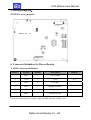
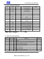
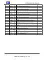
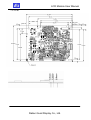
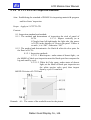
LCD MODULE SPECIFICATIONS
SPEC NO
GD56AUL
REV NO
Good Display
Good Display
Specifications
Type:
Model No.
Description:
Prepared:
Checked:
Approved:
Issue Date:
Standard
GD56AUL
5.6”, 320 x RGB x 234dots,
TFT LCD module.
With white LED backlight
VIDEO input.
Xiaoli Lan
Moon Wu
Boris Jen
2007.06.02
Dalian Good Display Co., Ltd.
Good Display
No.17 Gonghua Street, Shahekou District, Dalian 116021 China
Tel: +86-411-84619565 Fax: +86-411-84619585
E-mail: [email protected]
Website: www.good-lcd.com
www.good-lcd.com.cn
Dalian Good Display Co., Ltd.
1.03
LCD Module User Manual
Catalogue
Content
2
Version
3
1.Profile
4
2. Application
4
3. Main Parameter
4
4. Block Diagram、Product Picture
5
5. Wiring Diagram
6
6. Definition of Driver Board
6-8
7. Structural Diagram
9-10
8. 5.6" TFT- LCD PANEL Inspection Standard
11-12
9.Packing
13
10.Attention
13
Dalian Good Display Co., Ltd.
LCD Module User Manual
Version
Date
Version
Content
2007-3-23
VER: 1.00
The first
2007-5-13
VER: 1.01
The second
2007-6-2
VER: 1.03
The third
Dalian Good Display Co., Ltd.
LCD Module User Manual
1. Profile:
GD56AUL TFT LCD module is composed of GD56AUL driver board and
GTT056KDH01 panel. It provides users with VIDEO signal , with PAL and NTSC
system format(auto switch). It adopt IC to control power supply and backlight(LED backlight).
2. Application:
● Office Electric Equipment
● Instrument and Measure Equipment
● Machinery equipment
● Seeing and hearing equipment (Car display、Handy DVD、Long-distance terminal
and LCD TV)
● Family article for use (Seeing Doorbell, Seeing phone and digital camera)
● Don’t apply to high technology product that need dependable, stability and accuracy.
3. Main Parameter:
z
Product Name:5.6"TFT-LCD Module
z
Model:GD56AUL
z
Display:5.6" T F T p n a e l
z
z
Back light:LED
Pixel:320×3(RGB)×234
z
Vision bound:(U/D/L/R):(45/65/65/65)
z
Brightness:>250
z
System format:PAL/NTSC(Auto switch)
z
Signal input:1.0Vp-p 75 ohm
z
Voltage input:DC 12V±25%
z
Dimension of LCD (mm):113.28(W)×84.708(H)
z
Overall dimension of display (mm):126.5(W)×100(H)×5.7(D)
z
Structural dimension of PCB (mm):102.2(W)×82.4(H)×8.15(D)
z
Work temperature:- 3 0~ 8 5 ℃
z
Relative humidity:5~95% RH
z
Storage humidity:- 30℃~+ 8 5℃
cd/m2(put FPC line get off, you,just lighten backlight when test it.)
(12V
230mA±20mA)
Dalian Good Display Co., Ltd.
LCD Module User Manual
4. Block diagram:
Video decode
MCU
LCD
Driving
J201
Separate sync
VCOM
Color TFT LCD Module
Video
DC TO DC
DC TO DC
GD56AUL Module Picture:
Dalian Good Display Co., Ltd.
LED backlight
LCD Module User Manual
5. Wiring Diagram:
GD56AUL wiring diagram:
6. Connector Definition for Driver Board:
6.1J302 Connector Definition:
Pin no.
Symbol
In/Out
Description
1
COL-
I
Color reduce
2
COL
I
Color
3
COL+
I
Color plus
4
BRI-
I
Brightness reduce
5
BRI
I
Brightness
6
BRI+
I
Brightness plus
[Note1] It’s thick when the voltage is high, and thin when the voltage is low.
[Note2] It’s light when the voltage is high, and dark when the voltage is low.
Dalian Good Display Co., Ltd.
Remark
R:1
R:2
LCD Module User Manual
6.2 J201 Connector definition:
No.
Symbol
I/O
J201Pin description
1,2
+Vin
I
+12v power input
3,4
GND
-
Power ground
5
GNDS
-
Video signal ground
6
CONT
I
Contrast Input
7
VIDEO
I
Composite video signal input
8
BRI
I
Brightness control voltage
input
9
COL
I
Color control voltage input
10
L/R
I
Picture left/right inverse
control
11
TINT
I
Tint control voltage input
12
-HSY
O
Horizontal Sync Signal Input
13
-VSY
O
Vertical Sync Signal Input
14
Rin
I
Red Video Signal Input
15
Gin
I
Green Video Signal Input
16
Bin
I
Blue Video Signal Input
[Note] Usually use 4pin to
Remark
Note1
1、3、5、7 feet.
6.3 J401 Connector definition:
Pin No. Symbol
I/O
Function
1
GND
P
Ground
2
VCC
P
Supply voltage for logic control circuit scan driver
3
VGL
P
Negative power for scan driver
4
VGH
P
Positive power for scan driver
5
STVD
I/O
Vertical start pulse
6
STVU
I/O
Vertical start pulse
7
CKV
I
Shift clock input for scan driver
Dalian Good Display Co., Ltd.
Remar
LCD Module User Manual
8
U/D
I
UP/DOWN scan control input
9
OEV
I
Output enable control for scan driver
10
VCOM
I
Common electrode driving signal
11
VCOM
I
Common electrode driving signal
12
L/R
I
LEFT/RIGHT scan control input
13
MOD
I
Sequential sampling and simultaneous sampling setting
14
OEH
I
Output enable control for data driver
15
STHL
I/O
Start pulse for horizontal scan line
16
STHR
I/O
Start pulse for horizontal scan line
17
CPH3
I
Sampling and shifting clock pulse for data driver
18
CPH2
I
Sampling and shifting clock pulse for data driver
19
CPH1
I
Sampling and shifting clock pulse for data driver
20
VCC
P
Supply voltage for logic control circuit scan driver
21
GND
P
Ground
22
VR
I
Alternated video signal(Red)
23
VG
I
Alternated video signal(Green)
24
VB
I
Alternated video signal(Blue)
25
AVDD
P
Supply voltage for analog circuit
26
AVSS
P
Ground for analog circuit
Dalian Good Display Co., Ltd.
LCD Module User Manual
7. Structure Drawing:
7.1 LCD
Dalian Good Display Co., Ltd.
LCD Module User Manual
7.2 PCB:
Dalian Good Display Co., Ltd.
LCD Module User Manual
8. 5.6"TFT- LCD PANEL Inspection Standard:
Aim:Establishing the standard of PANLE for inspecting material & progress
and for clients’ inspection.
Scope:Apply to 5.6″TFT LCD
Content:
8.1. Inspection standard and method:
8.1.1. The method and determinant of inspecting the nick of panel of
LCD:
8.1.1.1. Inspect vertically (or at
45°angle from left/right)under the light tube (the power
is 20 W) in the distance of 30cm to the panel. If there is
no nick , it is “OK”. Otherwise “NG”.
8.1.2. The method and determinative for black & white & color spots for
the Panel of LCD:
8.1.2.1. Inspection methods
8.1.2.1.1. Black spots:under status of denote light,set
the MASK of black spot inspection near the black spot then compare the
big and small by eyes.
8.1.2.1.2. White & Color spots: under status of denote
light, set the Mask of black spot inspection on
the white spot(or color spot) then inspect
them by eyes if it can hide.
8.1.2.2. Division of LCD Panel
Remark:A1:The center of the available area for the picture
Dalian Good Display Co., Ltd.
LCD Module User Manual
A2:The edge of the available area for the picture(around the central area)
8.1.3. Determinant Choice
Allowed Area
Spot Diameter(mm)
A1
A2
Black d≤0.15
Irrespective
Irrespective
Spot
0.15<d≤0.3
4
4
0.3<d≤0.5
2
3
0.5<d≤0.8
0
2
White d≤0.15
Irrespective
Irrespective
or
0.15<d≤0.3
3
3
color
0.3<d≤0.5
1
2
spot
0.5<d≤0.8
0
1
Remark: 1. Size: Average Diameter=(Max. Diameter + Min. Diameter)/2
2. Using information above as a standard in order to judge while the spot
are dense.
3. Black & White spot:To judge the obvious spots through the change
of voltage by comparison。
4. Total quantity of Black & white & color spot: A1+A2 ≤ 4。
Dalian Good Display Co., Ltd.
LCD Module User Manual
9. Packing:
TBD
10. Attention:
1. The voltage of supply power don't exceed maxmium limit.
2. The connector can’t connect board in reverse, or the board will be burnt
and the products can't funtion well.
3. Please don’t touch it in order to keep your skin non-burn when you electrify
the board(there is high voltage on the board).
4. It is a electronic product, so you need to take anti-static measure when you
operate it.
5. 5.6”TFT-LCD panel is a glasswork, place carefully ,broken for fear.
6. The connection is “FPC”, which connect 5.6”TFT-LCD panel with PCB,
Please operate it carefully in order to keep it well.
7.Don't touch the pin of "variable resistor" when you adjust "VR".
Dalian Good Display Co., Ltd.