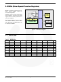
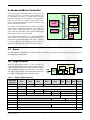
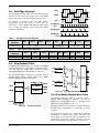
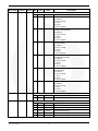
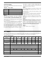
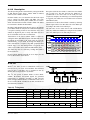
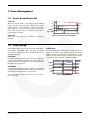
1
www.fairchildsemi.com AN-8202 FCM8531 User Manual Hardware Description 1. Summary The FCM8531 is an application-specific parallel-core processor for motor control that consists of an Advanced Motor Controller (AMC) processor and a MCS®51compatible MCU processor. The AMC is the core processor specifically designed for motor control, and more particularly it integrates a configurable processing core and peripheral circuits to perform Sensorless Field-Oriented Control (FOC) motor control. System control, user interface, communication interface, and input/output interface can be programmed through the embedded MCS®51 for different motor applications. The advantage of FCM8531’s parallel-core processors is that the two processors can work independently and complement each other. The AMC is dedicated for motor control applications, such as motor control algorithms, PWM control, current sensing, real-time over-current protection, and motor angle calculation. The embedded MCU provides motor control commands to the AMC to control motors through a communication interface. This approach reduces software burdens and simplifies control system programs because complex motor-control algorithms are executed in the AMC. Fairchild provides the Motor Control Development System (MCDS) IDE and MCDS Programming Kit for users to develop software, execute In System Programming (ISP), and perform online debugging. Figure 1 shows a typical application of the FCM8531. Advanced Motor Controller (AMC) Embedded MCU MCS®51 Compatible 63% of Instructions’ Execution Cycle < 3 System Clocks (3T) Memory Size: - 12K Bytes Flash Program Memory 256 +1K Bytes SRAM Data Memory Extended 16-Bit Multiplication / Division Unit (MDU) ≤17 General-Purpose Input / Output (GPIO) Pins Full Duplex Serial Interface (UART) I2C Interface Serial Peripheral Interface (SPI) Three External Interrupts Three 16-Bit Timers Programmable 15-Bit Watchdog Timer (WDT) Built-in Power-On Reset (POR) Built-in Clock Generator Two-Level Program Memory Lock ADC and DAC 8-Channel, 10-Bit ADC - Auto-Trigger Sample and Hold - Four Trigger Mode Selections - Three Pre-Amp Gain Selections 1 Channel, 8-Bit DAC Configurable Processing Core - Sensorless FOC with Speed Integral Method - Sensorless FOC with Sliding Mode - Hall Interface Space Vector Modulation (SVM) Sine-Wave and Square-Wave Generator Programmable Current Leading Phase Control Programmable Dead Time Protections Three-Level Over-Current Protection (OCP) Power Management IDLE Mode, STOP Mode, and SLEEP Mode Development Supports © 2013 Fairchild Semiconductor Corporation Rev. 1.0.0 • 2/18/13 In System Programming (ISP) On-Chip Debug Support (OCDS) www.fairchildsemi.com AN-8202 APPLICATION NOTE Figure 1. Application Block Diagram Figure 2. Block Diagram Figure 3. Pin Configuration © 2013 Fairchild Semiconductor Corporation Rev. 1.0.0 • 2/18/13 www.fairchildsemi.com 2 AN-8202 APPLICATION NOTE Table of Contents 1. Summary .............................................................................................................................................................. 1 2. MSFRs (Motor Special Function Registers) ........................................................................................................ 5 2.1. MSFRs Map ...............................................................................................................................................5 2.2. MSFRs Description ....................................................................................................................................6 3. Advanced Motor Controller ............................................................................................................................... 13 3.1. Reset .........................................................................................................................................................13 3.2. Angle Predictor ........................................................................................................................................13 3.2.2 Hall Signal Filter .........................................................................................................................14 3.2.3 Phase-Lock Loop (PLL)..............................................................................................................14 3.2.4 Leading Angle Shifter .................................................................................................................15 3.2.5 Angle Encoder.............................................................................................................................15 3.3. PWM Engine ............................................................................................................................................16 3.3.1 SAW Generator ...........................................................................................................................16 3.3.2 Square-Wave Mode.....................................................................................................................17 3.3.3 Sine-Wave Mode.........................................................................................................................19 3.3.4 Auto SAW Alignment Function..................................................................................................19 3.3.5 Dead Time ...................................................................................................................................19 3.4. Hall Edge Interrupt ...................................................................................................................................20 3.5. User-Defined Table ..................................................................................................................................20 3.5.1 User-Defined Square-Wave Table ..................................................................................................20 3.5.2 User-Defined Sine-Wave Table ..................................................................................................22 4. Embedded MCU ................................................................................................................................................ 23 4.1. Memory Organization ..............................................................................................................................23 4.1.1 Program Memory ........................................................................................................................23 4.1.2 Data Memory ..............................................................................................................................24 4.2. Reset .........................................................................................................................................................24 4.2.1 Power On Reset ...........................................................................................................................24 4.2.2 Hardware Reset ...........................................................................................................................25 4.2.3 Software Reset ............................................................................................................................25 4.3. SFRs (Special Function Registers)...........................................................................................................25 4.4. GPIO ........................................................................................................................................................38 4.4.1 GPIO Schematic ..........................................................................................................................38 4.4.2 Description ..................................................................................................................................38 4.5. Timer 0 .....................................................................................................................................................40 4.5.1 Block Diagram ............................................................................................................................40 4.5.2 Description ..................................................................................................................................40 4.6. Timer 1 .....................................................................................................................................................41 4.6.1 Block Diagrams...........................................................................................................................41 4.6.2 Description ..................................................................................................................................42 4.7. Timer 2 .....................................................................................................................................................42 4.7.1 Block Diagram ............................................................................................................................43 4.7.2 Description ..................................................................................................................................43 4.8. Interrupt ....................................................................................................................................................45 4.8.1 Description ..................................................................................................................................46 4.9. INT12 .......................................................................................................................................................48 4.9.1 Block Diagram ............................................................................................................................48 4.9.2 Description ..................................................................................................................................48 4.10. UART .......................................................................................................................................................49 4.10.1 Block Diagram ............................................................................................................................49 4.10.2 Description ..................................................................................................................................49 © 2013 Fairchild Semiconductor Corporation Rev. 1.0.0 • 2/18/13 www.fairchildsemi.com 3 AN-8202 5. 6. 7. 8. APPLICATION NOTE 4.11. SPI ............................................................................................................................................................51 4.11.1 Block Diagram ............................................................................................................................52 4.11.2 Description ..................................................................................................................................53 4.12. I2C ............................................................................................................................................................53 4.12.1 Block Diagram ............................................................................................................................54 4.12.2 Description ..................................................................................................................................54 4.13. MDU (Multiplication-Division Unit) .......................................................................................................55 4.13.1 Block Diagram ............................................................................................................................55 4.13.2 Description ..................................................................................................................................55 4.14. Watchdog .................................................................................................................................................57 4.14.1 Block Diagram ............................................................................................................................57 4.14.2 Description ..................................................................................................................................57 4.15. Mail Box ..................................................................................................................................................58 4.15.1 Block Diagram ............................................................................................................................58 4.15.2 Description ..................................................................................................................................58 4.16. Access MSFR ...........................................................................................................................................58 4.16.1 Description ..................................................................................................................................58 Analog Input / Output ........................................................................................................................................ 59 5.1. ADC .........................................................................................................................................................59 5.1.1 Block Diagram ............................................................................................................................59 5.1.2 Description ..................................................................................................................................60 5.2. DAC .........................................................................................................................................................61 5.2.1 Block Diagram ............................................................................................................................61 5.2.2 Description ..................................................................................................................................61 Protection ........................................................................................................................................................... 62 6.1. Fault Function ..........................................................................................................................................62 6.1.1 Block Diagram ............................................................................................................................62 6.1.2 Description ..................................................................................................................................62 6.2. Current Protection ....................................................................................................................................63 6.2.1 Block Diagram ............................................................................................................................63 6.2.2 Description ..................................................................................................................................63 Power Management ........................................................................................................................................... 65 7.1. Power On and Power Off .........................................................................................................................65 7.2. Power Saving ...........................................................................................................................................65 Development Supports ....................................................................................................................................... 66 8.1. MCDS (Motor Control Development System) ........................................................................................66 8.2. AMC Library............................................................................................................................................66 8.3. On-Chip Debug Support (OCDS) ............................................................................................................66 8.3.1 Description ..................................................................................................................................66 © 2013 Fairchild Semiconductor Corporation Rev. 1.0.0 • 2/18/13 www.fairchildsemi.com 4 AN-8202 APPLICATION NOTE 2. MSFRs (Motor Special Function Registers) MSFRs are registers used exclusively for motor control modules; those are accessed through SFRs. Parameters such as motor control, Hall signal configure, waveform type, PWM engine, and over-current protection level can be set in MSFRs. The Analog-to-Digital Converter (ADC) and controller statuses; such as Fault status, Hall status, and PWM status; can be obtained via MSFRs. Figure 4. MSFR Block Diagram 2.1. MSFRs Map Table 1. MSFRs Map Hex X000 X001 X010 X011 X100 X101 X110 X111 Hex 40 Reserved Reserved Reserved SLEEP OCH OCL SHORT DACO 47 38 Reserved Reserved Reserved Reserved Reserved Reserved ANGLE MSTAT 3F 30 ADC0L ADC0H ADC3L ADC3H 37 28 VAL VAH VBL VBH VCL VCH ADCINX Reserved 2F 20 IAL IAH IBL IBH ICL ICH OCCNTL OCSTA 27 18 HALMXU HALFLT HALSTA HALINT HPERL HPERM HPERH ADCCFG 1F 10 Reserved Reserved Reserved Reserved Reserved Reserved Reserved 17 08 PWMCFG SAWCNTL SPRDL SPRDH Reserved Reserved Reserved Reserved 0F 00 MCNTL ANGCTL AS ANGDET DUTYAL DUTYA Reserved Reserved 07 © 2013 Fairchild Semiconductor Corporation Rev. 1.0.0 • 2/18/13 www.fairchildsemi.com 5 AN-8202 2.2. APPLICATION NOTE MSFRs Description Table 2. Motor Special Function Registers (MSFRs) Byte Name Address Reset MCNTL 00h 00h ANGCTL AS ANGDET DUTYAL DUTYA PWMCFG 01h 02h 03h 04h 05h 08h © 2013 Fairchild Semiconductor Corporation Rev. 1.0.0 • 2/18/13 00h 00h 00h 00h Bit Type Name Motor Control 7 W 6 R/W 5 R/W Reserved AMC_RST SIN_TBL 4 R/W SQU_TBL 3:2 1 W R/W Reserved CW 0 R/W ST/FREE Angle Control 7 6 R/W Reserved ARNG 5 4:0 Reserved N/A W N/A Angle Shift 7 N/A 6:0 R/W N/A ANG Angle Predictor Configuration 7 R/W SIN_MAU 6 R/W SIN_EA 5 4:0 N/A W N/A Reserved Description Must Be Set to 0 Reset AMC Core, Active HIGH Sine-Wave Table Select 0: Default Sine-Wave Table 1: User-Defined Table Square-Wave Table Select 0: Default Square-Wave Table 1: User-Defined Table Must Be Set to 0 Rotation Direction 0: CCW 1: CW FREE or START 0: FREE 1: START Must Be Set to 0 Angle Predictor Range 0: Low-Speed 1: Normal Must Be Set to 0 N/A N/A Shift Angle 0 - 127 Mapping to 0 – 120° Sine-Wave Enable Mode 0: Automatically 1: Enabled by SIN_EA Sine-Wave Enable 0: Disabled 1: Enabled N/A Must Be Set to 0 DUTY Control 7:5 R/W DUTY[2:0] 4 3 2 1 0 N/A Reserved Reserved Reserved Reserved Square-Wave Mode: DUTY[2:0] Sine-Wave Mode: DUTY[2] N/A Must Be Set to 0 Must Be Set to 0 Must Be Set to 0 Must Be Set to 0 DUTY[10:3] DUTY[10:3] N/A W W W W 00h DUTY 7:0 R/W 00h PWM Configuration 7:6 R/W Reserved 5:4 R/W DT[1:0] Must Be Set to 0 Dead Time Setting www.fairchildsemi.com 6 AN-8202 Byte Name SAWCNTL SPRDL SPRDH APPLICATION NOTE Address Reset 09h 0Ah 0Bh 00h E0h FFh Bit Type Name 3 2 R/W R/W Reserved SYNCOFF 1 R/W WMC 0 W Reserved SAW Configuration 7 R/W ASCAL 00: 12 × tSYS (0.4 μs at 30 MHz) 01: 36 × tSYS (1.2 μs at 30 MHz) 10: 60 × tSYS (2.0 μs at 30 MHz) 11: 96 × tSYS (3.2 μs at 30 MHz) Must Be Set to 0 Synchronous Rectification (SR) 0: Enabled 1: Disabled Leading Angle Function in Square-Wave Mode 0: Disabled 1: Enabled Must Be Set to 0 Auto-scale 0: Disabled 1: Enabled SAW Mode 00: Disable 01: UP-DOWN Mode 10: UP Mode 11: DOWN Mode SAW Clock Pre-Scale 00: fSYS 01: fSYS/2 10: fSYS/4 11: fSYS/8 SAW Clock Post-Scale 000: 1 001: 1/2 010: 1/3 011: 1/4 100: 1/5 101: 1/6 110: 1/7 111: 1/8 6:5 R/W SAWMOD 4:3 R/W PRESCAL 2:0 R/W POSTCAL SAW Period 7:5 R/W 4:0 N/A SPRD[2:0] N/A SAW Period[2:0] N/A SAW Period 7:0 R/W SPRD[10:3] SAW Period[10:3] Must Be Set to 0 Must Be Set to 0 Reserved 0Ch - 11h 00h W Reserved Reserved 13h - 17h 00h W Reserved HALMUX 18h 00h © 2013 Fairchild Semiconductor Corporation Rev. 1.0.0 • 2/18/13 Description Hall Signal Inversion 7 N/A N/A 6 W Reserved 5 R/W HC_INV 4 R/W HB_INV 3 R/W HA_INV N/A Must Be Set to 1 Hall C Input Invert 0: Non-invert 1: Invert Hall B Input Invert 0: Non-invert 1: Invert Hall A Input Invert 0: Non-invert 1: Invert www.fairchildsemi.com 7 AN-8202 Byte Name APPLICATION NOTE Address Reset Bit 2:0 HALFLT HALSTA HALINT 19h 1Ah 1Bh 00h 00h 00h Type W Name Reserved Hall Configuration 7 R/W HAL_REG 6:4 R/W HAL_BNK 3 R/W HAL_AVG 2:0 R/W HAL_DEB Description Must Be Set to 0 Hall Regulation 0: Disabled 1: Enabled Hall Blanking Time 000: Disable 001: (5 - 6) × 1024 tSYS (170.7 - 204.8 μs at 30 MHz) 010: (9 - 10) × 1024 tSYS 011: (17 - 18) × 1024 tSYS 100: (33 - 34) × 1024 tSYS 101: (65 - 66) × 1024 tSYS 110: (129 - 130) × 1024 tSYS 111: (257 - 258) × 1024 tSYS Hall Period Average Mode 0: Disabled 1: Enabled Hall Debounce Time 000: Disabled (2 - 3 tSYS) 001: (2 - 3) × 64 tSYS (4.3 - 6.3 μs at 30 MHz) 010: (2 - 3) × 128 tSYS 011: (2 - 3) × 256 tSYS 100: (2 - 3) × 512 tSYS 101: (2 - 3) × 1024 tSYS 110: (2 - 3) × 2048 tSYS 111: (2 - 3) × 4096 tSYS Hall State 7:3 2 R 1 R Reserved HALL C_IN HALL B_IN Reserved Hall C Status In Angle Predictor Hall B Status In Angle Predictor 0 HALL A_IN Hall A Status In Angle Predictor R Hall Interrupt Configuration 7:4 N/A N/A 3:2 R/W HTMR_OUT 1:0 R/W HALL_INT N/A Hall Period Interrupt (EX8) 00: Disabled 01: If Hall Counter [17] = 1 10: If Hall Counter [18] = 1 11: If Hall Counter [19] = 1 Hall Edge Interrupt (EX10) 00: Disabled 01: Rise/Fall Edge 10: Rise Edge 11: Fall Edge HPERL 1Ch 00h Hall Period 7:0 R HPER [7:0] Hall Period [7:0] HPERM 1Dh 00h Hall Period 7:0 R HPER [15:8] Hall Period [15:8] Hall Period 7:4 N/A 3:0 R N/A HPER[19:16] N/A Hall Period [19:16] HPERH 1Eh © 2013 Fairchild Semiconductor Corporation Rev. 1.0.0 • 2/18/13 00h www.fairchildsemi.com 8 AN-8202 APPLICATION NOTE Byte Name Address Reset ADCCFG 1Fh 00h Bit Type Name ADC Configuration 7 W ADC_ST 6 5 N/A R/W N/A DAC_EA 4 R/W AD_CK 3:2 R/W FS_DIV 1:0 R/W ADC_TR Description ADC Signal Trigger Enable, ADC_TR= Timer Mode Only 0: N/A 1: ADC Convert Trigger (One Shot, Auto Clear) N/A DAC Output (To AOUT Pin) 0: Disabled 1: Enabled ADC Clock 0: fSYS/16 1: fSYS/32 Sampling Rate Divider 00: 1 01: 1/2 10: 1/4 11: 1/8 ADC Trigger Mode Select 00: SAW Top 01: SAW Bottom 10: TMR0 Overflow IAL 20h 0Ch ADC IA Configuration and ADC IA[1:0] 7:6 R IA [1:0] ADC IA [1:0] 5:4 N/A N/A N/A 3 W Reserved Must Be Set to 1 2 R/W Bias_A0 Bias Current 0: Disabled 1: Enabled 1:0 R/W GIA Pre-Amp Gain 00: ×1 01: ×2 10: ×4 IAH 21h 00h ADC IA[10:2] 7:0 R IBL 22h 0Ch ADC IB Configuration and ADC IB[1:0] 7:6 R IB [1:0] ADC IB [1:0] 5:4 N/A N/A N/A 3 W Reserved Must Be Set to 1 2 R/W Bias_B0 Bias Current 0: Disabled 1: Enabled 1:0 R/W GIB Pre-Amp Gain 00: ×1 01: ×2 10: ×4 IBH 23h 00h ADC IB[10:2] 7:0 R ICL 24h 0Ch ADC IC Configuration and ADC IC[1:0] 7:6 R IC [1:0] ADC IC [1:0] 5:4 N/A N/A N/A 3 W Reserved Must Be Set to 1 2 R/W Bias_C0 Bias Current 0: Disabled 1: Enabled © 2013 Fairchild Semiconductor Corporation Rev. 1.0.0 • 2/18/13 IA [10:2] IB [10:2] ADC IA [10:2] ADC IB [10:2] www.fairchildsemi.com 9 AN-8202 Byte Name APPLICATION NOTE Address Reset Bit 1:0 ICH 25h 00h Type R/W ADC IC[10:2] 7:0 R Name Description GIC Pre-Amp Gain 00: ×1 01: ×2 10: ×4 IC [10:2] ADC IC [10:2] OCCNTL 26h 00h Over-Current Protection Control Register 7:6 R/W OC_DEB OC Protection Debounce Time 00: 600 - 900 ns 01: 900 – 1200 ns 10: 1200 - 1500 ns 11: 1500 - 1800 ns 5 R/W OCCH_EA Phase C OCH Protection 0: Disabled 1: Enabled 4 R/W OCBH_EA Phase B OCH Protection 0: Disabled 1: Enabled 3 R/W OCAH_EA Phase A OCH Protection 0: Disabled 1: Enabled 2 R/W OCCL_EA Phase C OCL Protection 0: Disabled 1: Enabled 1 R/W OCBL_EA Phase B OCL Protection 0: Disabled 1: Enabled 0 R/W OCAL_EA Phase A OCL Protection 0: Disabled 1: Enabled OCSTA 27h 00h OC Protection State 7:6 N/A N/A 5 R OCCH 4 R OCBH 3 R OCAH 2 R OCCL 1 R OCBL 0 R OCAL N/A Phase C OCH Flag, Auto Clear after Read Phase B OCH Flag, Auto Clear after Read Phase A OCH Flag, Auto Clear after Read Phase C OCL Flag, Auto Clear after Read Phase B OCL Flag, Auto Clear after Read Phase A OCL Flag, Auto Clear after Read VAL 28h 00h ADC VA Configuration and ADC VA[1:0] 7:6 R VA [1:0] ADC VA[1:0] 5:2 N/A N/A N/A 1:0 R/W GVA Pre-Amp Gain 00: ×1 01: ×2 10: ×4 VAH 29h 00h ADC VA[10:2] 7:0 R 00h ADC VB Configuration and ADC VB[1:0] VBL 2Ah © 2013 Fairchild Semiconductor Corporation Rev. 1.0.0 • 2/18/13 VA [10:2] ADC VA[10:2] 7:6 R VB [1:0] ADC VB[1:0] 5:2 N/A N/A N/A www.fairchildsemi.com 10 AN-8202 Byte Name APPLICATION NOTE Address Reset Bit 1:0 VBH VCL VCH 2Bh 2Ch 2Dh 00h 00h 00h 2Eh 00h R/W ADC VB[10:2] 7:0 R 2Fh ADC0L 30h ADC0H 31h 00h 00h ADC3H 36h 37h 00h 00h 38h - 3Dh © 2013 Fairchild Semiconductor Corporation Rev. 1.0.0 • 2/18/13 00h Pre-Amp Gain 00: ×1 01: ×2 10: ×4 VB [10:2] ADC VB [10:2] VC [1:0] ADC VC [1:0] 5:2 N/A N/A N/A 1:0 R/W GVC Pre-Amp Gain 00: ×1 01: ×2 10: ×4 VC [10:2] ADC VC [10:2] ADC VC[10:2] R ADC Index Reserved Reserved 3:2 R AD_INX[3:2] Current ADC Channel Index 00: VA 01: VB 10: VC 11: ADC0 or ADC3 (need check AD_INX[1:0]) 1:0 R AD_INX[1:0] Index of ADC0/ADC3 00: ADC0 01: Reserved 10: Reserved 11: ADC3 Reserved Reserved ADC0 Configuration and ADC0[1:0] 7:6 R 5:2 N/A N/A N/A 1:0 R/W GADC0 Pre-Amp Gain 00: ×1 01: ×2 10: ×4 ADC0[1:0] ADC0[1:0] ADC0[10:2] ADC0[10:2] ADC0[10:2] R ADC3 Configuration and ADC3[1:0] 7:6 R 5:2 N/A N/A N/A 1:0 R/W GADC3 Pre-Amp Gain 00: ×1 01: ×2 10: ×4 ADC3[1:0] ADC3[1:0] ADC3 [10:2] 7:0 Reserved GVB R 7:0 ADC3L Description 7:6 7:4 Reserved Name ADC VC Configuration and ADC VC[1:0] 7:0 ADCINX Type R ADC3 [10:2] ADC3 [10:2] Reserved Reserved www.fairchildsemi.com 11 AN-8202 APPLICATION NOTE Byte Name Address Reset Bit ANGLE 3Eh 00h Angle Predictor Result 00h Motor Status 7:0 MSTAT 3Fh Type R VDD_TEST For Internal Testing R H_SLOW Hall Period Overflow 5 R SHORT_A IA SHORT 4 R SHORT_B IB SHORT 3 R SHORT_C IC SHORT 2 R H_ERR Hall Error (HA/HB/HC = 1/1/1 or 0/0/0) 1 R S_ACT 0 R DIR Operating Mode 0: Square-Wave 1: Sine-Wave Hall Direction Reserved SLEEP 43h 00h SLEEP Mode 7:3 N/A 2 W 1 W 0 R/W OCL SHORT DACO 45h 46h 47h © 2013 Fairchild Semiconductor Corporation Rev. 1.0.0 • 2/18/13 10h FFh 00h 0 - 191 Mapping to 0 – 360° R 00h FFh ANGLE 6 40 - 42h 44h Description 7 Reserved OCH Name N/A Reserved Reserved Sleep Positive OC Protection Level 7:0 R/W OCH Negative OC Protection Level 7:0 R/W OCL SHORT Detection Level 7:0 R/W SHORT AOUT Output Level 7:0 R/W DACO N/A Must Be Set to 1 Must Be Set to 0 SLEEP Mode 0: Disabled 1: Enabled Positive OC Protection Level (00h - FFh mapping to 0 – 4 V) Negative OC Protection Level (00h - FFh Mapping to 0 - 4 V) SHORT Detection Level (00h - FFh Mapping to 0 - 4 V) AOUT Output Level (00h - FFh Mapping to 0 4 V) www.fairchildsemi.com 12 AN-8202 APPLICATION NOTE 3. Advanced Motor Controller The Advanced Motor Controller (AMC) is used for driving motors that consist of several motor control modules, such as configurable processing core, PWM engine, and angle predictor. Depending on the application, the configurable processing core can be configured with suitable AMC library to perform different motor control algorithms, such as FOC and sensorless control. For example, if the Sensorless library is used as the control algorithm, the configurable processing core obtains the motor current via the internal ADC to estimate the rotor angle. After that, the PWM engine provides PWM output drive signals to set the correct rotor angle. If the configurable processing core is configured with the Hall Interface library, the rotor position information is inputted through the GPIO and the rotor angle is estimated by the angle predictor. The PWM engine can provide the appropriate PWM output drive signals for driving motors. Figure 5. AMC Block Diagram 3.1. Reset The AMC_RST bit of MSFR MCNTL (00h) is used to reset the AMC processing core. Resetting the AMC processing core in the initial stage is recommended. 3.2. Angle Predictor When the Hall Interface library is used for Sine-wave control, the Hall signal is used to accurately predict the rotor angle of the motor. This predicted angle provides the Space Vector Modulation (SVM) to generate space vector pulses. The angle predictor includes a Hall signal filter, Phase-Lock Loop (PLL), leading angle shifter, and angle encoder. Figure 6. Table 3. Angle Block Diagram Angle Predictor Registers Byte Name (Address) Bit 7 Bit 6 Bit 5 ANGCTL (01h) Reserved ARNG Reserved AS (02h) N/A ANGDET (03h) SIN_MAU SIN_EA N/A HALMUX (18h) N/A Reserved HC_INV HALFLT (19h) HAL_REG Bit 4 Bit 3 Bit 2 Bit 1 Bit 0 N/A 00h ANG HAL_BNK HALSTA (1Ah) HALINT (1Bh) © 2013 Fairchild Semiconductor Corporation Rev. 1.0.0 • 2/18/13 Reserved 00h HAL_AVG HAL_DEB 00h HALL_IN HTMR_OUT HPER[7:0] HPERM (1Dh) ANGLE (3Eh) 00h HA_INV Reserved N/A HPERL (1Ch) HPERH (1Eh) 00h Reserved HB_INV 00h 00h HPER[19:16] ANGLE 00h HALL_INT 00h HPER[15:8] N/A Reset 00h 00h www.fairchildsemi.com 13 AN-8202 APPLICATION NOTE 3.2.2 Hall Signal Filter Functions of the Hall signal filter, set by the MSFR HALFLT (19h), include the debounce, blanking, Hall signal regulation, Hall signal average, and Hall signal inversion. Debounce: Noises or bounces may be involved in input signals, usually resulting in incorrect angle prediction. The MSFR HALFLT (19h) can set the debounce time to filter out the involved noises. While the input signal is changing, the debounce function holds the signal for a debounce time until the change is confirmed (see Figure 7). e e Figure 9. Hall Regulation Figure 7. Hall Filter Debounce Average: The value stored in the Hall period register represents the time of the most recent 60-degree electrical angle based on the system clock. A digital filter is enabled by the average function to reduce the variation of periods. It is invoked by setting MSFR HALFLT (19h)[3]. Blanking: Users can set the blanking time through the HALFLT. Hall signals are not allowed to be updated for a blanking time once a change in the Hall signal is confirmed (see Figure 8). Invert: Set MSFR HALMUX (18h)[5:3] to invert the Hall signal before entering the PLL (see Figure 10). e e Figure 8. Hall Filter Blanking Regulation: This feature makes PWM outputs remain its current state if the Hall signals return to its previous state. Figure 10. Hall Invert Without Hall regulation; when Hall signals the return to the previous states (see Figure 9), the PWM output returns to previous state (corresponding to Hall state), so the PWM U output is off. However, with the Hall regulation, the PWM U remains in the current state and keeps outputting the PWM signal. 3.2.3 Phase-Lock Loop (PLL) The PLL uses Hall signals as input signals and detects changes in every 60-degree electrical angle to predict the rotor position. The motor starts in Square-Wave Mode then enters Sine-Wave Mode once the PLL locks the Hall signals. There are two modes for entering the Sine-wave driving. Automatic Mode (Default): MSFR ANGDET (03h)[7:6] = b’00. Once the rotation speed is stable and higher than the required minimum speed, the PWM drive signal is automatically changed from SquareWave Mode to Sine-Wave Mode. If the rotation speed is unstable or is below the required minimum speed, it exits Sine-Wave Mode. The enter/exit condition can be set by MSFR ANGDET (03h)[4:0]. © 2013 Fairchild Semiconductor Corporation Rev. 1.0.0 • 2/18/13 www.fairchildsemi.com 14 AN-8202 APPLICATION NOTE Manual Mode: MSFR ANGDET (03h)[7:6] = b’11. The PWM signal is forced to drive in Sine-Wave Mode. This mode is not recommended. Figure 11. There are two selectable frequency ranges for the Hall signal input: Low-Speed Mode (PLL clock = fSYS/64) and Normal Mode (PLL clock = fSYS/4). Fairchild recommends using Normal Mode for general motor applications. LowSpeed Mode can be selected for very low-speed operations. Table 4. Hall Period Register - 1 When Hall Frequency Range = Normal Mode PLL Clock Period → 4 / (30 × 106) = 0.133 (μs) (0.476 ms) / (0.133 μs) = 3578.94 (000DFAh) Angle Predictor Range (fSYS = 30 MHz) ANGCTL (01h)[6] Mode Hall Frequency 0 Low-Speed 0.1 – 360 Hz 1 Normal 1.5 – 1200 Hz Figure 12. The conversion between Hall frequency and motor speed is defined in the following formula: RPM 120 Hallfreq. Poles Hall Period Register – 2 3.2.4 Leading Angle Shifter As the motor is rotating, a phase lag ( θ) between current and Back Electromotive Force (BEMF) may occur because of the motor’s winding inductance. Generally, the phase lag gets larger as the speed increases and the phase lag affects motor efficiency. Usually, the best performance is achieved once the current and the BEMF are in phase (see Figure 13). (1) where poles is number of magnetic poles in the motor. The Hall Period register is a 20-bit counter that represents the time of the last 60-degree electrical angle based on the system clock. MSFR HPERL (1Ch) stores bits 0 - 7; MSFR HPERM (1Dh) stores bits 8 - 15; MSFR HPERH (1Eh) stores bits 16 - 19. An example is given below to show how a Hall period is converted to real rotation speed in RPM. Example: Hall Period Register = 000515h,System Clock = 30 MHz, Motor-Pole = 4 Hall Frequency Range = Low Speed Mode PLL Clock Period → 64 / (30 × 106) = 2.133 (μs) Hall Period Register 000515h = 1301 (Hexadecimal to Decimal) Figure 13. Phase Shift 1301 × 2.133 = 2.775033 (ms / 60°), 2.775033 × 6 = 16.650198 (ms / 360°) The leading angle shifter is capable of compensating the phase lag by shifting PWM ahead. MSFR AS (02h) is a 7bit register that can set the leading angle shifting from 0 to 120° ahead. 1 / 16.65 ≈ 60 (Hz), Hall Frequency = 60 (Hz) RPM 120 60 4 1800 RPM The resolution could be insufficient while the motor is rotating at very high speed; however, switching the frequency mode to the Normal Mode improves it by using higher PLL clock frequency. An example is given below to show the difference between the two modes. Example: System Clock=30 MHz, Hall Frequency = 350 Hz When Hall Frequency Range=Low Speed Mode Figure 14. Angle Shift PLL Clock Period → 64 / (30 × 106)=2.133 (μs) 3.2.5 Angle Encoder Hall Period = 1 / 350=2.857 (ms / 360°), 2.857 / 6=0.476 (ms / 60°) The PWM engine outputs PWM signals according to the angle encoder. The angle encoder sums the PLL calculation results and the leading angle shifter setting in one angle, MSFR ANGLE (3Eh). (0.476 ms) / (2.133 μs)=223.16 (0000DFh) © 2013 Fairchild Semiconductor Corporation Rev. 1.0.0 • 2/18/13 www.fairchildsemi.com 15 AN-8202 APPLICATION NOTE 3.3. PWM Engine The motor starts in Square-Wave Mode, and then enters into Sine-Wave Mode once the PLL locks the Hall signals. By setting the MSFR ANGDET (03h), users can determine whether the PWM engine is working in Square-Wave Mode or Sine-Wave Mode after the PLL is in lock (refer to Section 3.2.3.) The PWM engine includes four circuit modules: SAW generator, square-wave PWM generator, sine-wave PWM generator, and PWM MUX. Table 5. PWM Engine Registers Byte Name (Address) Bit 7 ANGDET (03h) SIN_MAU DUTYAL (04h) Bit 6 Bit 5 SIN_EA N/A DUTY[2:0] Bit 4 SAWCNTL (09h) SPRDL (0Ah) Bit 2 Bit 1 Bit 0 Reserved N/A 00h DUTY[10:3] Reserved ASCAL DT[1:0] SAWMOD Reserved 00h SYNCOFF PRESCAL SPRD[2:0] WMC Reserved POSTCAL N/A SPRDH (0Bh) SPRD[10:3] Figure 15. Reset 00h Reserved DUTYA (05h) PWMCFG (08h) Bit 3 00h 00h E0h FFh PWM Block Diagram 3.3.1 SAW Generator There are three modes of carrier waveforms: Up Mode, Down Mode, and Up-Down Mode; selected by the SAWMOD bit in MSFR SAWCNTL (09h) (see Figure 17). The clock source of the SAW generator is provided from the result of the system clock passing through two frequency dividers: pre-scale module and post-scale module. It provides the pulses (SAW clock) for the 11-bit counter inside the SAW generator (see Figure 16). Figure 17. SAW Mode In Up-Down Mode: fPWM = SAW Clock / (SAW Period × 2) (2) In Up Mode or Down Mode: fPWM = SAW Clock / SAW Period (3) Figure 16. Pre-Scale and Post-Scale © 2013 Fairchild Semiconductor Corporation Rev. 1.0.0 • 2/18/13 www.fairchildsemi.com 16 AN-8202 APPLICATION NOTE As shown in Figure 19, when a count value of the PWM ontime is the same as that of the SAW period, PWM has the largest on-time. The on-time setting should fall into the range of the SAW period. The SAW period is determined by MSFR SPRDH (0Bh) and MSFR SPRDL (0Ah) (11-bit, left aligned), as shown in Figure 18. Shift the actual SAW Period five bits left before writing it into the registers. The PWM duty ratio resolution is a ratio to SAW period. The resolution gets higher when SAW period increases. Figure 18. SAW Period Register Figure 19. PWM Output The pre-scale and the post-scale are set by MSFR SAWCNTL (09h)[4:0]. The formula and the description of SAWCNTL are: SAW Clock Frequency = fSYS / (Post-Scale × Pre-Scale) Appropriate PWM output signals are determined by the pattern of the Hall input signals or the Hall register, while direction is determined by the CW setting. (4) Table 6 shows PWM output signals in each Hall status regarding to CW. Example: To obtain an Up-Down Mode PWM frequency of 20 kHz when the system frequency is 30 MHz (from Equation (2)): Table 6. Defaulted Square-Wave PWM Output CW Hall Status (HA HB HC) U-V-W X-Y-Z X 000 000 000 X 111 000 000 1 001 P00 Pb 1 0 1 011 00P 0 1 Pb 3.3.2 Square-Wave Mode 1 010 00P 1 0 Pb The square-wave PWM generator generates square-wave PWM signals and its default pattern is based on the built-in default square-wave table. 1 110 0P0 1 Pb 0 1 100 0P0 0 Pb 1 SAW Period = 30 MHz / (20 kHz × 2) = 750 = 2EEh The SAW period corresponding to a 20 kHz PWM frequency, 750 (2EEh in hexadecimal), is determined. Shift “2EEh” five bits left and the result is “5DC0h”. Write 5Dh and C0h into registers SPRDH (0Bh) and SPRDL (0Ah) to complete the setting. In addition to generating default square-wave PWM output waveforms, a customizable user-define square-wave table is also provided so that users can define customized squarewave waveforms according to application requirements. The motor starts in Square-Wave Mode and remains in Square-Wave mode after PLL is in lock if the highest two bits of ANGDET (03h)[7:6] are set to b’10. 1 101 P00 Pb 0 1 0 101 00P 1 0 Pb 0 100 00P 0 1 Pb 0 110 P00 Pb 1 0 0 010 P00 Pb 0 1 0 011 0P0 0 Pb 1 0 001 0P0 1 Pb 0 Notes: 1. X: Don’t care 2. P: PWM 3. Pb: PWM inverse The PWM on-time in a PWM duty is proportional to a ratio of the DUTY[10:0] to the SAW period. For example, when the DUTY[10:0] = 200h and the SAW period = 400h; the PWM on-time = 50%. Similarly, the PWM on-time = 25% when the SAW period = 800h. The DUTY[10:0] in Square-Wave Mode is an 11-bit register, which is composed of DUTYA (05h) and the highest three bits of DUTYAL (04h). DUTYA is a high-order byte. © 2013 Fairchild Semiconductor Corporation Rev. 1.0.0 • 2/18/13 www.fairchildsemi.com 17 AN-8202 APPLICATION NOTE Figure 20. Square-Wave Mode (CW = 1) Figure 21. Square-Wave Mode (CW = 0) Figure 22. Sine-Wave Mode © 2013 Fairchild Semiconductor Corporation Rev. 1.0.0 • 2/18/13 www.fairchildsemi.com 18 AN-8202 APPLICATION NOTE In Table 6 above, the Pb (PWM inverse) can be turned off by disabling the Synchronous Rectification function. It is invoked by setting MSFR PWMCFG (08h)[2]. The default is enabled. 3.3.3 Sine-Wave Mode Figure 22 shows that the modulation waveform (blue curve) is generated from the SVM table according to the predicted angle. The modulation waveform is compared with the SAW to produce a sine-wave PWM signal. The amplitude of the modulation waveform is determined by DUTY[10:2] register. Unlike the Square-Wave Mode, the DUTY[1:0] is neglected in the Sine-Wave Mode. 3.3.4 Auto SAW Alignment Function If the auto SAW alignment feature is turned on in the MSFR SAWCNTL, DUTY’s highest bit (bit 10) aligns with the valid highest bit of the SAW period. It is convenient for users to control the duty ratio through only a byte of register, DUTYA, without shifting. Example: The SAW period is an 11-bit register. For simplicity, it is left-shifted five bits. For example, when SAW period = 3FFh, it becomes 7FE0h. So does DUTY[10:0] and 5-bit shifted DUTY[10:0] is called DUTY. When auto SAW alignment is turned off and the PWM mode is Square-Wave Mode; if the SAW period is 7FE0h, set DUTY= 7FE0h to get PWM output with the largest duty (see Figure 23). Figure 23. Auto SAW Alignment Disabled When the Auto SAW Alignment is turned on, however, users should set DUTY = FFC0h for the largest duty because DUTY is aligned to the first valid bit of the SAW Period (see Figure 24). Figure 25. Auto SAW Alignment Function 3.3.5 Dead Time Dead time is set in the MSFR PWMCFG (08h). This feature can prevent the inverter from burning out caused by cross conduction between high side and low side. The value of dead time is set according to rising/falling time of the inverter (FETs or IGBTs). Figure 24. Auto SAW Alignment Enabled When auto SAW alignment is on, the relationship between DUTY and the SAW is shown in Figure 25. Figure 26. Dead Time © 2013 Fairchild Semiconductor Corporation Rev. 1.0.0 • 2/18/13 www.fairchildsemi.com 19 AN-8202 3.4. APPLICATION NOTE Hall Edge Interrupt Through MSFR HALINT (1Bh), users can enable Hall edge interrupt and can choose three trigger types: rising/falling trigger, rising trigger, and falling trigger (see Figure 27). An interrupt is triggered when the Hall signal’s rising/falling matches the setting of HALL_INT. Set HALL_INT = b’00 to disable Hall Edge interrupt. Please note, to enable the interrupt, beside HALL_INT, EX10 should be enabled either. Figure 27. Hall Edge Interrupt Trigger Mode Table 7. Hall Signal Control Registers Byte Name (Address) Bit 7 Bit 6 HALINT (1Bh) Table 8. Bit 5 Bit 4 Bit 3 N/A HTMR_OUT Bit 1 Bit 0 HALL_INT Reset 00h User-Defined Table Registers Byte Name (Address) Bit 7 Bit 6 Bit 5 Bit 4 MCNTL (00h) Reserved AMC_RST SIN_TBL SQU_TBL 3.5. Bit 2 Bit 3 Bit 2 Reserved Bit 1 Bit 0 Reset CW ST/FREE 00h User-Defined Table In addition to the default square-wave and sine-wave PWM output waveforms, two customizable user-defined squarewave and sine-wave PWM output waveforms can be achieved through the user-defined table (see Table 8). The user-defined table is located in a particular area of program memory, 2F00h - 2FFEh, which is set by MSFR MCNTL (00h)[5:4], as shown in Figure 29. Figure 29. User-Defined Table Block Diagram 3.5.1 User-Defined Square-Wave Table User-defined square-wave table is located in 2FC0h 2FCDh, totally including 12 addresses. The first six addresses are corresponding to CW = 1 and the last six addresses are corresponding to CW = 0. Figure 28. User-Defined Table Each byte in the six bytes represents a particular 60-degree electrical angle corresponding to a Hall status, as shown in Table 9. The stored codes are from 0 to 5, which represent different combinations of high/low-side signals. The table only defines phase U, but signals for phase V and phase W are automatically generated by shifting 120-degree and 240degree electrical angle referring to phase U, respectively. © 2013 Fairchild Semiconductor Corporation Rev. 1.0.0 • 2/18/13 www.fairchildsemi.com 20 AN-8202 Table 9. APPLICATION NOTE User-Defined Square-Wave PWM Address CW Hall Status (HA HB HC) 2FC0h 1 001 2FC1h 1 011 2FC2h 1 010 2FC3h 1 110 2FC4h 1 100 Code High Side Low Side 2FC5h 1 101 0 OFF OFF 2FC6h 0 101 1 OFF ON 2FC7h 0 100 2 ON OFF 2FC8h 0 110 4 PWM /PWM 2FC9h 0 010 5 /PWM PWM 2FCAh 0 011 2FCBh 0 001 2FCCh X 000 2FCDh X 111 Code Example: The required PWM is shown in Figure 30. Figure 30. Required Waveforms Users can fill fields in the high-side/low-side with the required waveform in Table 10 according to appropriate Hall signals and the CW. Users can find code values corresponding to the combination of high-side and low-side PWM signals and fill the code value up in Table 9. These codes must be stored in program memory 2FC0h to 2FCDh. Table 10. User-Defined Square-Wave Table Address (Example) Address CW Hall Status (HA HB HC) Code High-Side Low-Side 2FC0h 1 001 2FC1h 1 011 2 ON OFF 0 OFF OFF 2FC2h 1 010 5 /PWM PWM 2FC3h 2FC4h 1 110 1 OFF ON 1 100 0 OFF OFF 2FC5h 1 101 4 PWM /PWM 2FC6h 0 101 1 OFF ON 2FC7h 0 100 0 OFF OFF 2FC8h 0 110 4 PWM /PWM 2FC9h 0 010 2 ON OFF 2FCAh 0 011 0 OFF OFF 2FCBh 0 001 5 /PWM PWM 2FCCh X 000 0 OFF OFF 2FCDh X 111 0 OFF OFF © 2013 Fairchild Semiconductor Corporation Rev. 1.0.0 • 2/18/13 www.fairchildsemi.com 21 AN-8202 APPLICATION NOTE 3.5.2 User-Defined Sine-Wave Table Therefore, the users can fill in the “Entered Values” column in Table 11 to describe required modulation waveform according to appropriate electrical angles. The user-defined sine-wave table is located in program memory 2F00h - 2FBFh and the 192 addresses are corresponding to the 360-degree electrical angles. The electrical angle 0º is located in 2F00h and aligned to the rising edge of Hall A. Table 11. User-Defined Sine-Wave Table Address (Example) Users can fill the addresses with the value 0 - 31 to describe the modulation waveform. The table only defines phase U, but signals for phase V and phase W are automatically generated by shifting 120-degrees and 240-degrees from phase U, respectively. Example: To output a trapezoidal waveform, the required modulation waveform is similar to Figure 31. Address Electrical Angle Entered Values Notes 2F00h - 2F1Fh 0 – 59° 0 No Amplitude 2F20h - 2F3Fh 60 – 119° 0 - 31 Increasing Step by Step 2F40h - 2F5Fh 120 – 179° 31 Maximum Amplitude 2F60h - 2F7Fh 180 - 239° 31 Maximum Amplitude 2F80h - 2F9Fh 240 - 299° 31 - 0 Decreasing Step by Step 2FA0h - 2FBFh 300 - 359° 0 No Amplitude These codes must be stored in program memory 2F00h to 2FBFh. Figure 31. Required Modulation Waveform © 2013 Fairchild Semiconductor Corporation Rev. 1.0.0 • 2/18/13 www.fairchildsemi.com 22 AN-8202 APPLICATION NOTE 4. Embedded MCU The instruction sets of the embedded MCU of FCM8531 are fully compatible with MCS®51. Users can develop software with standard 805x assemblers and compilers. The embedded MCU uses Advanced Instruction Architecture (AIA) to significantly enhance performance. Compared with a traditional 8051, 63% of AIA’s execution cycle are less than three (3) system clocks (3T). In addition to the existing 8051 MCU functions; such as GPIO, TIMER 0/1/2, ISR, and UART; other communication interfaces; such as SPI, I2C, and WDT (Watchdog Timer); are also integrated into the embedded MCU. In addition, the On-Chip Debug Support (OCDS), In-System Programming (ISP), and Improved Multiply-Divide Unit (MDU) modules are provided for system debugging, program downloading, and faster computing. The embedded MCU is capable of accessing data in MSFRs and transferring data to the AMC through the Special Function Registers (SFRs). Figure 32. Embedded MCU Block Diagram 4.1. Memory Organization 4.1.1 Program Memory Similar to the standard 8051, FCM8531 memory is divided into two parts: the program memory and the data memory. The 12 K-byte flash memory in the embedded MCU is with ISP functionality, which allows the program code to be updated online. The flash memory is divided into two parts, the program code area and special-purpose area. Addresses 0000h - 2EFFh define the program code area; addresses higher than 2EFFh define the special-purpose area, which includes the user-defined wave table and a lock byte. The OCDS function is disabled if the most significant bit of Lock byte is 0. The flash memory is encrypted when other bits in the Lock byte are 0. The embedded MCU has 12 K-byte of flash memory as the program memory. Internal data memory and external data memory are composed of 256-byte and 1 K-byte high-speed Static Random-Access Memory (SRAM). The data in flash memory must first be erased to FFh before being overwritten. Note: In the ISP mode, pins P12 and P13 become ISP functional pins. To assure running ISP properly, do not set the two pins as Direct Driver Mode. The capacitance on these two pins must be as small as possible. Although the SFR CKCON register can adjust the Wait State for program memory and data memory, the recommendation is to set the highest speed (CKCON = 00h) for the best performance. During power on or reset, the program starts at the program memory’s address to 0000h. The embedded MCU provides Figure 33. Memory Map of Embedded MCU © 2013 Fairchild Semiconductor Corporation Rev. 1.0.0 • 2/18/13 www.fairchildsemi.com 23 AN-8202 APPLICATION NOTE 4.1.2 Data Memory 16 interrupts. The vectors of the interrupt service routines are distributed over the program memory at addresses 0003h - 00ABh. When an interrupt occurs, the program automatically jumps to the appropriate interrupt vector to execute the interrupt service subroutine. Interrupt vectors are shown in Table 12: The data memory of the embedded MCU is divided into two parts: 256-byte internal data memory and 1 K-byte external data memory. The first 128 bytes (00h - 7Fh) in internal data memory are permitted to directly access address, which include four register banks, Bit Map Address, and a generalpurpose direct addressing area. The last 128 bytes (80h FFh) in data memory are overlapped with SFR to access the SFR when direct addressing; whereas it reads and writes the SRAM when indirect addressing. Table 12. Interrupt Vectors Interrupt Source Interrupt Vector Symbol External Interrupt 0 0003h EX0 Timer 0 Overflow 000Bh ET0 External Interrupt 1 0013h EX1 Timer 1 Overflow 001Bh ET1 Serial 0023h ES0 Timer 2 002Bh ET2 2 IC 0043h EX7 SPI 004Bh EX2 COM0 0053h EX3 COM1 005Bh EX4 COM2 0063h EX5 FAULT 008Bh EX8 ADC Ready 0093h EX9 Hall Edge 009Bh EX10 AMC 00A3h EX11 External Interrupt 12 00ABh EX12 The size of the external data memory is 1 K-byte. Use the MOVX instruction to indirectly address through the Data Pointer (DPTR) or R0/R1 (Page Mode) so that more instruction cycles are required to access the data. Figure 34. Data Memory 4.2. Reset There are three reset methods: Power On Reset (POR), software reset, and Reset by a high-level input on RST pin. After reset, P0[7:2] is set as PWM outputs and are in lowlevel initially. P1[7:0] and P2[6:4] are set as open-drain outputs and is pulled HIGH initially. The program begins executing from the address 0000h stored in the SFR PC. The accumulator and flags are cleared and other registers are set to the initial state. 4.2.1 Power On Reset When VDD exceeds VDD_ON, the operation of the voltage generator module begins to provide the required power to the internal circuitry of the FCM8531. Afterward, the Power On Reset (POR) functionality is enabled and the clock generator starts. About two milliseconds later, the reset status is removed and the MCU program begins executing. © 2013 Fairchild Semiconductor Corporation Rev. 1.0.0 • 2/18/13 Figure 35. Power-On Reset Sequence www.fairchildsemi.com 24 AN-8202 APPLICATION NOTE 4.2.2 Hardware Reset 4.2.3 Software Reset When the switch is pressed, the reset pin is set to HIGH and the FCM8531 enters Reset state, where the reset pin returns to LOW and the FCM8531 begins executing the program when the switch is released and the RC time has passed. Internal software reset functionality is set through SFR SRST (F7h) to reset the embedded MCU. Figure 36. Hardware Reset 4.3. SFRs (Special Function Registers) The SFRs in the embedded MCU of the FCM8531use direct addressing access. Table 13. Special Function Registers Map Hex X0h/X8h X1h/X9h X2h/XAh X3h/XBh X4h/XCh X5h/XDh X6h/XEh F8 P0_CFG IO_CFG INT12_CFG INT12_STA DRV0 DRV1 DRV2 F0 B E8 MD0 E0 ACC D8 ADCON D0 PSW C8 T2CON C0 IRCON B8 IEN1 B0 SPSTA MD1 MD2 MD3 SPCON SPDAT SPSSN I2CDAT I2CADR I2CCON MD4 MD5 X7h/XFh Hex FF SRST F7 ARCON EF E7 I2CSTA DF D7 CRCL CRCH TL2 TH2 CCEN CCL1 CCH1 CCL2 CCH2 IP1 SRELH MTX0 MTX1 MTX2 A8 IEN0 IP0 SRELL A0 P2 98 SCON 90 P1 88 TCON TMOD TL0 TL1 TH0 TH1 CKCON 80 P0 SP DPL DPH DPL1 DPH1 WDTREL MTX3 MRX0 MRX1 CF C7 MRX2 IRCON2 BF MRX3 B7 AF A7 SBUF IEN2 DPS © 2013 Fairchild Semiconductor Corporation Rev. 1.0.0 • 2/18/13 9F DPC MSFRADR MSFRDAT 97 8F PCON 87 www.fairchildsemi.com 25 AN-8202 APPLICATION NOTE Table 14. Special Function Register Description Byte Name Address Reset Bit P0 80h FFh Port 0 7:0 SP 81h 07h 82h 00h 83h 84h 85h PCON 86h 87h 88h DPH Data Pointer High Byte 00h Data Pointer 1 High Byte 08h 00h © 2013 Fairchild Semiconductor Corporation Rev. 1.0.0 • 2/18/13 Stack Point Data Pointer Low Byte 00h 00h Port 0 DPL R/W R/W R/W R/W DPL1 DPH1 Data Pointer 1 Low Byte Data Pointer 1 High Byte Watchdog Timer Reload Register 7 R/W WDPS 6:0 R/W WDTPER Pre-scale Select 0: Normal Scale 1: 1/16 Scale When set, the watchdog is clocked through an additional pre-scale (divide by 16) Watchdog Reload Value Reload value for the highest seven bits of the watchdog timer. This value is loaded to the watchdog timer when a refresh is triggered by a consecutive setting of bits WDT (IEN 0.6) and SWDT (IEN 1.6) Power Control 7 R/W SMOD 6 R/W WDT_TM 5 R/W ISR_TM 4:2 TCON SP Data Pointer 1 Low Byte 7:0 WDTREL R Data Pointer High Byte 7:0 DPH1 P0 [7:0] 00h 7:0 DPL1 R/W Description Data Pointer Low Byte 7:0 DPH Name Stack Point 7:0 DPL Type Reserved Serial Port Baud-Rate Select (Baud-Rate Double) 0: fSYS/64 1: fSYS/32 Watchdog Timer Test Mode Flag 0: Watchdog is clocked through a pre-scale (fSYS/12) 1: Skip pre-scale (Test Mode Only) Interrupt Service Routine Test Mode Flag Must Be Set to 0 1 R/W STOP STOP Mode Control 0 R/W IDLE IDLE Mode Control Timer/Counter Control Register 7 R/W TF1 6 R/W TR1 5 R/W TF0 4 R/W TR0 3 R/W IE1 Timer 1 Overflow Flag TF1 is set by hardware when Timer 1 overflows It can be cleared by software and is automatically cleared when entering interrupt Timer 1 Run Control 0: Stop 1: Run Timer 0 Overflow Flag TF0 is set by hardware when Timer 0 overflows. It can be cleared by software and is automatically cleared when entering interrupt. Timer 0 Run Control 0: Stop 1: Run External Interrupt 1 Flag 2 R/W IT1 External Interrupt 1 Type Control www.fairchildsemi.com 26 AN-8202 Byte Name TMOD TL0 APPLICATION NOTE Address 89h 8Ah Reset Bit 8Bh R/W IE0 0 R/W IT0 00h 8Ch 7 R/W GATE1 6 R/W C/T1 5:4 R/W T1MOD 3 R/W GATE0 2 R/W C/T0 1:0 R/W T0MOD 00h Timer 0, Low Byte 00h Timer 1, Low Byte 00h 8Dh 00h 8Eh 71h R/W R/W Timer 1 Gate Control 0: Disabled External Gate Control 1: Enabled External Gate Control (pin INT1). When INT1 is HIGH and TR1 is set, the counter 1 is increased every falling edge of pin T1. Timer 1 Counter / Timer Select 0: Timer Mode 1: Counter Mode (incremented every falling edge on T1 pin) Timer 1 Mode Control 00: 13-bit Counter / Timer, five lower bits in TL1, eight bits in TH1 01: 16-bit Counter / Timer 10: 8-bit Auto-Reload Counter / Timer. Reload value is TH1. 11: Timer 1 is stopped Timer 0 Gate Control 0: Disabled External Gate Control. 1: Enabled External Gate Control (pin INT0). When INT0 is HIGH and TR0 is set, the counter 0 is increased every falling edge of pin T0. Timer 0 Counter / Timer Select 0: Timer Mode 1: Counter Mode (incremented every falling edge on T0 pin) Timer 0 Mode Control 00: 13-bit Counter / Timer, with five lower bits in TL0 and eight bits in TH0 01: 16-bit Counter / Timer 10: 8-bit Auto-Reload Counter / Timer. The reload value is in TH0. 11: Timer 0 acts as two independent 8-bit Timer / Counter TL0,TH0 TL0 Timer 0, Low Byte TL1 Timer 1, Low Byte R/W TH0 Timer 0, High Byte R/W TH1 Timer 1, High Byte N/A Clock Control Register 7 N/A N/A 6:4 R/W PMCYC 3 N/A N/A 2:0 © 2013 Fairchild Semiconductor Corporation Rev. 1.0.0 • 2/18/13 External Interrupt 0 Type Control 0: Low-Level Trigger 1: Falling-Edge Trigger Timer 1, High Byte 7:0 CKCON 0: Low-Level Trigger 1: Falling-Edge Trigger External Interrupt 0 Flag Timer 0, High Byte 7:0 TH1 Description Timer Mode Control Register 7:0 TH0 Name 1 7:0 TL1 Type R/W XRAMCYC Program Memory Wait State Control N/A External Data Memory Stretch Cycle Control www.fairchildsemi.com 27 AN-8202 APPLICATION NOTE Byte Name Address Reset Bit P1 90h FFh Port 1 7:0 DPS 92h 00h MSFRADR 93h 96h 00h 00h 97h 00h 98h 00h © 2013 Fairchild Semiconductor Corporation Rev. 1.0.0 • 2/18/13 P1 [7:0] N/A Description Port 1 N/A N/A Bank Switch Enable (Enable RS0,RS1 of PSW) 3 R/W BSE R/W DPSEL2 DPSEL1 DPSEL0 Data Point Register Select Data Point Control Register 7:6 N/A N/A 5:3 R/W DPC[5:3] 2 R/W DPC[2] 1 R/W DPC[1] 0 R/W DPC[0] N/A Next Data Pointer Selection Auto-Modification Size 0: The current DPTR is automatically modified by 1 after each MOVX@DPTR instruction when DPC[0] = 1. 1: The current DPTR is automatically modified by 2 after each MOVX@DPTR instruction when DPC[0] = 1. Auto-Modification Direction 0: The current DPTR is automatically incremented after each MOVX@DPTR instruction when DPC[0] = 1. 1: The current DPTR is automatically decremented after each MOVX@DPTR instruction when DPC[0] = 1. Auto-Modification Enable When set, the current DPTR is automatically incremented after each MOVX@DPTR instruction. MSFR Address (00h - 7Fh) R/W MSFRADR MSFR Address (00h - 7Fh) Access MSFR Data 7:0 SCON R/W 2:0 7:0 MSFRDAT Name Data Pointer Select Register 7:4 DPC Type R/W MSFRDAT MSFR Data Serial Port, Control Register Serial Port Mode Select (SM0, SM1) 00: Shift Register, fSYS/12 (Mode 0) 01: 8-bit UART, Variable (Mode 1) 10: 9-bit UART (Mode 2) SMOD=0 fSYS/64, SMOD=1 fSYS/32 11: 9-bit UART, Variable (Mode 3) 7:6 R/W SM0 and SM1 5 R/W SM2 Multiprocessor Communication Enable 4 R/W REN 3 R/W TB8 2 R/W RB8 Serial Reception Enable 0: Disabled 1: Enabled Transmitter Bit 8 This bit is used while transmitting data through serial port in Mode 2 or Mode 3. The state of this bit corresponds with the state of the 9th transmitted bit, such as parity check or multiprocessor communication. It is controlled by software. Received Bit 8 This bit is used while receiving data through serial port in th Mode 2 or Mode 3. It reflects the state of the 9 received bit. In Mode 1, if multi-processor communication is enabled (SM2=0), this bit is the Stop bit. In Mode 0, this bit is not used. www.fairchildsemi.com 28 AN-8202 Byte Name SBUF APPLICATION NOTE Address 99h Reset 00h Bit Type Name Description 1 R/W TI 0 R/W RI Transmit Interrupt Flag It indicates completion of a serial transmission at serial port. It is set by hardware at the end of bit 8 in Mode 0 or at the beginning of a Stop bit in other modes. It must be cleared by software. Receive Interrupt Flag It is set by hardware after completion of a serial reception at serial port. It is set by hardware at the end of bit 8 in Mode 0 or in the middle of a Stop bit in other modes. It must be cleared by software. Serial Port, Data Buffer 7:0 IEN2 9Ah 00h R/W Reserved 5 R/W EX12 4 R/W EX11 3 R/W EX10 2 R/W EX9 1 R/W EX8 0 A0h FFh A8h 00h © 2013 Fairchild Semiconductor Corporation Rev. 1.0.0 • 2/18/13 Reserved Must Be Set to 0 External Interrupt 12 0: Disabled 1: Enabled AMC Interrupt (Interrupt 11) 0: Disabled 1: Enabled Hall Edge Interrupt (Interrupt 10) 0: Disabled 1: Enabled ADC Interrupt (Interrupt 9) 0: Disabled 1: Enabled Fault Interrupt (Interrupt 8) 0: Disabled 1: Enabled Must Be Set to 0 Port 2 7:0 IEN0 Serial Port, Data Buffer Interrupt Enable Register 2 7:6 P2 SBUF [7:0] R/W P2 [7:0] Port 2 Interrupt Enable Register 0 7 R/W EA 6 R/W WDT 5 R/W ET2 4 R/W ES0 3 R/W ET1 2 R/W EX1 1 R/W ET0 Interrupts Enable When set to 0, all interrupts are disabled. Otherwise, enable each interrupt by setting the corresponding Interrupt Enable bit. Watchdog Timer Refresh Flag Set to initiate / refresh the watchdog timer (see Section 4.14) Timer 2 Interrupt 0: Disabled 1: Enabled Serial Port Interrupt 0: Disabled 1: Enabled Timer 1 Overflow Interrupt 0: Disabled 1: Enabled External Interrupt 1 0: Disabled 1: Enabled Timer 0 Overflow Interrupt 0: Disabled www.fairchildsemi.com 29 AN-8202 Byte Name IP0 APPLICATION NOTE Address A9h Reset 00h Bit Type Name 0 R/W EX0 Description 1: Enabled External Interrupt 0 0: Disabled 1: Enabled Interrupt Priority Register 0 7 Reserved 6 R/W WDTS 5:0 R/W IP0 [5:0] Must Be Set to 0 Watchdog Timer Status Flag Set by hardware when the watchdog timer reset occurs Interrupt Priority See IP1 SRELL AAh D9h Serial Port Reload Register Low Byte (Baud-Rate generator) 7:0 R/W SREL[7:0] Serial Port Reload Register [7:0] MTX0 B0h 00h Data Sent to AMC 7:0 MTX1 B1h 00h B2h 00h B3h 00h B4h 00h B5h 00h B6h 00h B7h 00h B8h 00h R/W R R R R Data Sent to AMC MTX3 Data Sent to AMC MRX0 Data Received from AMC MRX1 Data Received from AMC MRX2 Data Received from AMC MRX3 Data Received from AMC Interrupt Enable Register 1 7 R/W EXEN2 Timer 2 External Reload Interrupt 0: Disabled 1: Enabled 6 R/W SWDT Watchdog Timer Start / Refresh Flag (see Section 4.14) 5 © 2013 Fairchild Semiconductor Corporation Rev. 1.0.0 • 2/18/13 MTX2 Data Received from AMC 7:0 IEN1 R/W Data Received from AMC 7:0 MRX3 Data Sent to AMC Data Received from AMC 7:0 MRX2 MTX1 Data Received from AMC 7:0 MRX1 R/W Data Sent to AMC 7:0 MRX0 Data Sent to AMC Data Sent to AMC 7:0 MTX3 MTX0 Data Sent to AMC 7:0 MTX2 R/W Reserved 4 R/W EX5 3 R/W EX4 2 R/W EX3 1 R/W EX2 0 R/W EX7 Must Be Set to 0 CC2 Interrupt 0: Disabled 1: Enabled CC1 Interrupt 0: Disabled 1: Enabled CC0 Interrupt 0: Disabled 1: Enabled SPI Interrupt 0: Disabled 1: Enabled 2 I C Interrupt 0: Disabled 1: Enabled www.fairchildsemi.com 30 AN-8202 APPLICATION NOTE Byte Name Address Reset IP1 B9h 00h Bit Type IRCON2 BAh BFh 03h 00h © 2013 Fairchild Semiconductor Corporation Rev. 1.0.0 • 2/18/13 Description Interrupt Priority Register 1 7:6 SRELH Name Reserved 5 R/W 4 R/W 3 R/W 2 R/W 1 R/W 0 R/W Must Be Set to 0 Timer 2 Interrupt / External Interrupt 12 Priority Setting. [IP1.5:IP0.5]= 00: Level 0, Lowest 01: Level 1 10: Level 2 11: Level 3, Highest Serial Port Interrupt / External Interrupt 5 / External Interrupt 11 Priority Setting. [IP1.4:IP0.4]= 00: Level 0, Lowest 01: Level 1 10: Level 2 11: Level 3, Highest Timer 1 Interrupt / External Interrupt 4 / External Interrupt 10 Priority Setting. [IP1.3:IP0.3]= 00: Level 0, Lowest 01: Level 1 10: Level 2 11: Level 3,Highest External Interrupt 1 / External Interrupt 3 / External Interrupt 9 Priority Setting. [IP1.2:IP0.2]= 00: Level 0, Lowest 01: Level 1 10: Level 2 11: Level 3, Highest Timer 0 Interrupt / External Interrupt 2 / External Interrupt 8 Priority Setting. [IP1.1:IP0.1]= 00: Level 0, Lowest 01: Level 1 10: Level 2 11: Level 3, Highest External Interrupt 0 / External Interrupt 7 Priority Setting. [IP1.0:IP0.0]= 00: Level 0, Lowest 01: Level 1 10: Level 2 11: Level 3, Highest Serial Port Reload Register High Byte (Baud-Rate Generator) 7:2 N/A N/A 1:0 R/W SREL [9:8] N/A Serial Port Reload Register [9:8] Interrupt Request Control 2 Register N/A 7:5 N/A N/A 4 R/W IEX12 External Interrupt 12 Flag 3 R/W IEX11 External Interrupt 11 Flag 2 R/W IEX10 External Interrupt 10 Flag 1 R/W IEX9 External Interrupt 9 Flag 0 R/W IEX8 External Interrupt 8 Flag www.fairchildsemi.com 31 AN-8202 APPLICATION NOTE Byte Name Address Reset IRCON C0h 00h Bit Type C1h 00h 7 R/W EXF2 6 R/W TF2 Reserved C2h C3h C4h External Interrupt 5 Flag 3 R/W IEX4 External Interrupt 4 Flag 2 R/W IEX3 External Interrupt 3 Flag 1 R/W IEX2 External Interrupt 2 Flag 0 R/W IEX7 External Interrupt 7 Flag Compare/Capture Enable Register C5h Reserved Must Be Set to 0 Compare / Capture Mode for CC2 Register 00: Compare / capture disable 01: Capture on rising edge at pin CC2 10: Compare enabled 11: Capture on write operation into register CC2 Compare / Capture Mode for CC1 Register 00: Compare / capture disable 01: Capture on rising edge at pin CC1 10: Compare enabled 11: Capture on write operation into register CC1 Compare / Capture Mode for CRC Register 00: Compare / capture disable 01: Capture on rising edge at pin CC0 10: Compare enabled 11: Capture on write operation into register CC0 5:4 R/W COCAH2 / COCAL2 3:2 R/W COCAH1 / COCAL1 1:0 R/W COCAH0 / COCAL0 00h Compare / Capture Register 1, Low Byte 00h Compare / Capture Register 1, High Byte 00h 00h C6 - C7h 00h T2CON C8h 00h CCH1 R/W CCL2 R/W CCH2 Reserved Compare / Capture Register 1, LOW Byte Compare / Capture Register 1, HIGH Byte Compare / Capture Register 2, LOW Byte Compare / Capture Register 2, HIGH Byte Must Be Set to 0 Timer 2 Control Register 7 R/W T2PS 6 R/W I3FR 5 R/W I2FR 4:3 R/W T2R[1:0] 2 © 2013 Fairchild Semiconductor Corporation Rev. 1.0.0 • 2/18/13 R/W CCL1 Compare / Capture Register 2, High Byte 7:0 Reserved R/W Compare / Capture Register 2, Low Byte 7:0 CCH2 Must Be Set to 0 IEX5 7:0 CCL2 Timer 2 Overflow Flag R/W 7:0 CCH1 Timer 2 External Reload Flag 4 7:6 CCL1 Description Interrupt Request Control Register 5 CCEN Name Reserved Pre-Scale Select 0: Timer 2 is cocked by fSYS /12 1: Timer 2 is clocked by fSYS /24 Active Edge Selection for External Interrupt 3 0: Falling Edge 1: Rising Edge Active Edge Selection for External Interrupt 2 0: Falling edge 1: Rise edge Timer 2 Reload Mode Selection 0X: Reload disabled 10: Mode 0 11: Mode 1 Must Be Set to 0 www.fairchildsemi.com 32 AN-8202 Byte Name CRCL APPLICATION NOTE Address CAh Reset 00h Bit Type Name Description 1:0 R/W T2I[1:0] Timer 2 Input Selection (T2I1,T2I0) 00: Timer 2 stopped 01: Input frequency = fSYS/12 or fSYS/24 10: Timer 2 is increased by falling edge of pin T2 11: Input frequency (fSYS/12 or fSYS/24) gated by pin EXT2 Compare/Reload/Capture Register, Low Byte 7:0 CRCH CBh CCh CDh 00h Timer 2, Low Byte 00h ADCON D0h D8h 00h 00h R/W R/W R/W DAh 00h I2CCON DBh DCh 00h 00h Timer 2, LOW Byte TH2 Timer 2, HIGH byte R/W CY Carry Flag 6 R/W AC Auxiliary Carry Flag General-Purpose Flag 0 5 R/W F0 4:3 R/W RS1 RS0 [RS1,RS0] Selection Register Bank Locations 00: bank 0 (00h - 07h) 01: bank 1 (08h - 0Fh) 10: bank 2 (10h - 17h) 11: bank 3 (18h - 1Fh) 2 R/W OV Overflow Flag 1 R/W F1 General-Purpose Flag 1 0 R P Parity Flag Serial Port Baud-Rate Select Register Serial Port Baud-Rate Selection (in Mode 1 and 3) 7 R/W BD When 1, additional internal baud-rate generator is used. Otherwise baud-rate is sourced by Timer 1. Reserved Must Be Set to 0 2 I C Data Register R/W I2CDAT I2C Data I2C Address 7:1 R/W I2C address 0 R/W GC I2C Address in Slave Mode Address Acknowledge 2 I C Control Register 7 R/W CR2 6 R/W ENS1 5 R/W 4 © 2013 Fairchild Semiconductor Corporation Rev. 1.0.0 • 2/18/13 TL2 7 7:0 I2CADR Compare / Reload / Capture Register, HIGH Byte Program Status Word Register 6:0 I2CDAT CRCH Timer 2, High byte 7:0 PSW Compare / Reload / Capture Register, LOW Byte Compare/Reload/Capture Register, High Byte 7:0 TH2 CRCL 00h 7:0 TL2 R/W R/W STA STO Clock Rate Bit 2 I2C Activate 0: Disabled 1: Enabled START Flag 2 2 When STA = 1, the I C component checks the I C bus status and if the bus is free, a START condition is generated. STOP Flag 2 When STO = 1, the I C interface is in Master Mode, a 2 STOP condition is transmitted to the I C bus. www.fairchildsemi.com 33 AN-8202 Byte Name I2CSTA ACC APPLICATION NOTE Address DDh E0h Reset F8h 00h Bit Type Name Description 3 R/W SI 2 R/W AA Serial Interrupt Flag The SI is set by hardware when one of 25 out of 26 2 possible I C states is entered. The only state that does not set the SI is F8h, which indicates that there is no available relevant state information. It must be cleared by software. Assert Acknowledge Flag Define Acknowledge level 0: LOW level 1: HIGH level 1 R/W CR1 Clock Rate Bit 1 0 R/W CR0 Clock Rate Bit 0 I2C Status Register R I2CSTA 2:0 N/A N/A N/A ACC Accumulator Serial Peripheral Data Transfer Flag Set by hardware upon data transfer completion. Cleared by hardware when data transfer is in progress. Can be also cleared by reading the SPSTA register with the SPIF bit set, then reading the SPDAT register. Write Collision Flag Set by hardware upon write collision to SPDAT. Cleared by hardware upon data transfer completion when no collision has occurred. Can be also cleared by an access to SPSTA register and an access to SPDAT register. Synchronous Serial Slave Error Flag Set by hardware when SPSSN input is deserted before the end of receive sequence. Cleared by disabling the SPI module (clearing SPEN bit in SPCON register). Accumulator 7:0 SPSTA E1h 00h R/W SPI Status Register 7 R SPIF 6 R WCOL 5 R SSERR 4:0 SPCON E2h Reserved 34h Must Be Set to 0 SPI Control Register 7 R/W SPR2 6 R/W SPEN SPI Clock Rate See SPR[1:0] SPI Activate 0: Disabled 1: Enabled Reserved Must Be Set to 0 5 © 2013 Fairchild Semiconductor Corporation Rev. 1.0.0 • 2/18/13 I2C Status Register 7:3 4 R/W MSTR 3 R/W CPOL 2 R/W CPHA SPI Mode 0: Slave Mode 1: Master Mode Clock Polarity 0: The SCK is set to 0 in Idle state. 1: The SCK is set to 1 in Idle state. Clock Phase 0: Data are sampled when the SCK leaves the Idle state 1: Data are sampled when the SCK returns to Idle state www.fairchildsemi.com 34 AN-8202 Byte Name SPDAT APPLICATION NOTE Address E3h Reset 00h Bit Type Name 1:0 R/W SPR[1:0] MD0 E4h E9h FFh 00h EAh 00h EBh 00h ECh 00h N/A N/A 0 R/W SSR SPI Slave Select Register Multiplication / Division Register 0 EDh 00h EEh 00h B EFh F0h 00h 00h P0_CFG F7h F8h 00h 00h © 2013 Fairchild Semiconductor Corporation Rev. 1.0.0 • 2/18/13 R/W MD1 Multiplication / Division Register 1 R/W MD2 Multiplication / Division Register 2 R/W MD3 Multiplication / Division Register 3 Multiplication / Division Register 4 R/W MD4 Multiplication / Division Register 4 Multiplication / Division Register 5 R/W MD5 Multiplication / Division Register 5 Arithmetic Control 7 R MDEF 6 R MDOV 5 R/W SLR 4:0 R/W SC[4:0] MDU Error Flag Indicates an improperly performed operation (when one of the arithmetic operations has been restarted or interrupted by a new operation). MDU Overflow Flag Overflow occurrence in the MDU operation Shift Direction 0: Left 1: Right Shift Counter ( SC[4]: MSB, SC[0]: LSB) SC[4:0] = 0, Normalize function SC[4:0] ≠ 0, Shift function B Register 7:0 SRST Multiplication / Division Register 0 Multiplication / Division Register 3 7:0 ARCON MD0 Multiplication / Division Register 2 7:0 MD5 R/W Multiplication / Division Register 1 7:0 MD4 SPI Data Register N/A 7:0 MD3 SPDAT 7:1 7:0 MD2 R/W SPI Slave Select Register 7:0 MD1 SPI Clock Rate [SPR2,SPR1,SPR0]= 010: fSYS/8 011: fSYS/16 100: fSYS/32 101: fSYS/64 110: fSYS/128 111: Master clock is not generated. SPI Data Register 7:0 SPSSN Description R/W B B Register Software Reset Register 7:1 N/A N/A 0 R/W SRSTREG N/A Software Reset Request P0 Configuration 7 R/W P07_IO 6 R/W P06_IO P07 IO Type 0: PWM Z Channel 1: GPIO P06 IO Type 0: PWM W Channel 1: GPIO www.fairchildsemi.com 35 AN-8202 Byte Name APPLICATION NOTE Address Reset Bit Type Name 5 R/W P05_IO 4 R/W P04_IO 3 R/W P03_IO 2 R/W P02_IO 1:0 IO_CFG INT12_CFG INT12_STA F9h FAh FBh 00h P05 IO Type 0: PWM Y Channel 1: GPIO P04 IO Type 0: PWM V Channel 1: GPIO P03 IO Type 0: PWM X Channel 1: GPIO P02 IO Type 0: PWM U Channel 1: GPIO Reserved Must Be Set to 0 IO Configuration 7:6 R/W 5:4 R/W 3:2 R/W 1:0 R/W EI_CFG[1:0] INT0, INT1 Pin Assignment 00: Reserved 01: Reserved 10: P24INT0, P25INT1 11: P26INT0 I12_CFG[1:0] INT12 Edge Trigger Type 00: Disable 01: Rising / Falling 10: Rising 11: Falling P2_CFG[1:0] P2 Configuration Refer to Table [P2_CFG1:P2CFG0] P1_CFG[1:0] P1 Configuration Refer to Table [P1_CFG1:P1_CFG0] 00h INT12 Sourced Pin Assignment 7 R/W ASI_OSC INT12 Assign to OSC Check 6 R/W ASI_P16 INT12 Assign to P16 5 R/W ASI_P15 INT12 Assign to P15 4 R/W ASI_P14 INT12 Assign to P14 3 R/W ASI_P13 INT12 Assign to P13 2 R/W ASI_P12 INT12 Assign to P12 1 R/W ASI_P11 INT12 Assign to P11 0 R/W ASI_P10 INT12 Assign to P10 00h © 2013 Fairchild Semiconductor Corporation Rev. 1.0.0 • 2/18/13 Description INT12 State, to identify INT12 trigger source 7 R ST_OSC INT12 is triggered by OSC Check 6 R ST_P16 INT12 is triggered by P16 5 R ST _P15 INT12 is triggered by P15 4 R ST _P14 INT12 is triggered by P14 3 R ST _P13 INT12 is triggered by P13 2 R ST _P12 INT12 is triggered by P12 1 R ST _P11 INT12 is triggered by P11 0 R ST _P10 INT12 is triggered by P10 www.fairchildsemi.com 36 AN-8202 Byte Name DRV0 APPLICATION NOTE Address FCh Reset 00h Bit Type DRV2 FDh FEh 00h 00h 7 R/W P07_DRV 6 R/W P06_DRV 5 R/W P05_DRV 4 R/W P04_DRV 3 R/W P03_DRV 2 R/W P02_DRV Reserved 0: Open drain with internal pull-down resistor 1: Direct drive 0: Open drain with internal pull-down resistor 1: Direct drive 0: Open drain with internal pull-down resistor 1: Direct drive 0: Open drain with internal pull-down resistor 1: Direct drive 0: Open drain with internal pull-down resistor 1: Direct drive 0: Open drain with internal pull-down resistor 1: Direct drive Must Be Set to 0 GPIO 1 Driver Mode Select 7 R/W P17_ DRV 6 R/W P16_ DRV 5 R/W P15_ DRV 4 R/W P14_ DRV 3 R/W P13_ DRV 2 R/W P12_ DRV 1 R/W P11_ DRV 0 R/W P10_ DRV 0: Open drain with internal pull-up resistor 1: Direct drive 0: Open drain with internal pull-up resistor 1: Direct drive 0: Open drain with internal pull-up resistor 1: Direct drive 0: Open drain with internal pull-up resistor 1: Direct drive 0: Open drain with internal pull-up resistor 1: Direct drive 0: Open drain with internal pull-up resistor 1: Direct drive 0: Open drain with internal pull-up resistor 1: Direct drive 0: Open drain with internal pull-up resistor 1: Direct drive GPIO 2 Driver Mode Select 7 Reserved Must Be Set to 0 0: Open drain with internal pull-up resistor 1: Direct drive 0: Open drain with internal pull-up resistor 1: Direct drive 0: Open drain with internal pull-up resistor 1: Direct drive 6 R/W P26_DRV 5 R/W P25_DRV 4 R/W P24_DRV 3:0 © 2013 Fairchild Semiconductor Corporation Rev. 1.0.0 • 2/18/13 Description GPIO 0 Driver Mode Select 1:0 DRV1 Name Reserved Must Be Set to 0 www.fairchildsemi.com 37 AN-8202 APPLICATION NOTE 4.4. GPIO The FCM8531 has three GPIO ports: P0[7:2], P1[7:0], and P2[6:4], which can be set as direct drive or open drain through DRV0, DRV1, and DRV2 of the SFR. P0[7:2] are pulled down to GND by internal resistors and other digital IOs are pulled up to 5 V with internal resistors. Table 15. GPIO Registers Byte Name (Address) Bit 7 Bit 6 Bit 5 Bit 4 Bit 3 Bit 2 P0 (80h) P07 P06 P05 P04 P03 P02 P13 P12 P1 (90h) P17 P16 P15 P14 P2 (A0h) Reserved P26 P25 P24 P0_CFG (F8h) P07_IO P06_IO P05_IO P04_IO P03_IO P02_IO IO_CFG (F9h) EI_CFG1 EI_CFG0 I12_CFG1 I12_CFG0 P2_CFG1 P2_CFG0 DRV0 (FCh) P07_DRV P06_DRV P05_DRV P04_DRV P03_DRV P02_DRV DRV1 (FDh) P17_DRV P16_DRV P15_DRV P14_DRV P13_DRV P12_DRV DRV2 (FEh) Reserved P26_DRV P25_DRV P24_DRV Bit 1 Bit 0 Reset Reserved P11 FFh P10 FFh Reserved FFh Reserved P1_CFG1 00h P1_CFG0 Reserved P11_DRV 00h 00h P10_DRV Reserved 00h 00h 4.4.1 GPIO Schematic Figure 37. GPIO 4.4.2 Description P0[7:2] can be defined as a GPIO or PWM output signal (U, V, W, X, Y, and Z) by using P0_CFG of the SFR. After reset, P0[7:2] is pre-set to a PWM output signal and other DIO pins are pre-set as the GPIO. Multi-functional pins P1[7:0] and P2[6:4] can be set through IO_CFG (F9h) of the SFR (see Table 16 and Table 17). Set SFR IO_CFG (F9h)[1:0] to configure P1[7:0] and distribute the serial bus (SPI Mode, I2C Mode, UART Mode). Table 16. P1_CFG[1:0] CFG[1:0] 00 (Default) 01 10 11 P17 P16 SCK MISO P15 P14 P13 MOSI SPSSN / TDO SDA SPI / OCDS SCK MISO SDA SCL MOSI TX P11 SCL TX I2C SPSSN / TDO TX RX SCK SPI / OCDS RX SDA MISO MOSI UART RX UART SDA RX SCL I2C SPSSN / TDO SPI / OCDS SCL I2C SCK MISO MOSI SPSSN / TDO SPI / OCDS P2[6:4] are set, by default, to be as GPIO pins. The DRV2 (FEh) register selects either open drain or direct driver. According to different purposes, the IO_CFG (F9h) register © 2013 Fairchild Semiconductor Corporation Rev. 1.0.0 • 2/18/13 P10 UART UART TX I2C P12 is set to distribute the timer input (Timer 0, Timer 1, Timer 2) pin assignment as shown in Table 17 below. www.fairchildsemi.com 38 AN-8202 APPLICATION NOTE Table 17. P2_CFG[1:0] CFG[1:0] P26 CC2 00 (Default) P25 P24 CC1 CC0 Capture and Compare CC2 01 CC1 CC0 Capture and Compare 10 11 T2 T1 T0 TMR2 TMR1 TMR0 T0 T2EX T2 TMR0 TMR2 P1[6:0] can also be configured as an input pin of External Interrupt 12 (see Table 18). Users can turn on INT12 and choose the Trigger Type by setting IO_CFG (F9h)[5:4]. Table 18. INT 12_CFG I12CFG[1:0] = 01, 10, 11 (Enable INT12) INT12_CFG [7:0] INT12_CFG [7] OSC check assigned to INT12 INT12_CFG [6] P16 assigned to INT12 INT12_CFG [5] P15 assigned to INT12 INT12_CFG [4] P14 assigned to INT12 INT12_CFG [3] P13 assigned to INT12 INT12_CFG [2] P12 assigned to INT12 INT12_CFG [1] P11 assigned to INT12 INT12_CFG [0] P10 assigned to INT12 P2[6:4] can also be configured as an input pin of External Interrupt 0 or External Interrupt 1 by SFR IO_CFG (F9h)[7:6] as shown in Table 19. Table 19. EI_CFG[1:0] CFG[1:0] P26 10 11 P25 P24 External Interrupt 1 External Interrupt 0 External Interrupt 0 The GPIO pins include P0[7:2], P1[7:0], and P2[6:4], and P1 and P2 pins are set as shown in Table 20. Table 20. All GPIO Configuration and Function Pin P1_CFG=00 P2_CFG=00 P1_CFG=01 P2_CFG=01 P1_CFG=10 P2_CFG=10 P1_CFG=11 P2_CFG=11 I12CFG[1:0]≠00 INT12_CFG=7Fh P10 RX SCL SPSSN SPSSN INT12 P11 TX SDA MOSI MOSI INT12 P12 SCL RX MISO MISO INT12 P13 SDA TX SCK SCK INT12 P14 SPSSN SPSSN RX SCL INT12 P15 MOSI MISO TX SDA INT12 P16 MISO MISO SCL RX INT12 P17 SCK SCK SDA TX © 2013 Fairchild Semiconductor Corporation Rev. 1.0.0 • 2/18/13 EI_CFG [1:0]= 10 EI_CFG [1:0]= 11 www.fairchildsemi.com 39 AN-8202 APPLICATION NOTE Pin P1_CFG=00 P2_CFG=00 P1_CFG=01 P2_CFG=01 P1_CFG=10 P2_CFG=10 P1_CFG=11 P2_CFG=11 P24 CC0 CC0 T0 T2 INT0 P25 CC1 CC1 T1 T2EX INT1 P26 CC2 CC2 T2 T0 4.5. Timer 0 Timer 0 is a 16-bit timer/counter determined in Timer Mode or Counter Mode by SFR TMOD (89h). In Timer Mode, its counter value is increased by one for every 12 system cycles. In Counter Mode, a counter value is Table 21. I12CFG[1:0]≠00 INT12_CFG=7Fh EI_CFG [1:0]= 10 EI_CFG [1:0]= 11 INT0 increased by one when each falling edge on the T0 pin. The maximum frequency on T0 cannot exceed fSYS/2 because a falling edge (HIGH-to-LOW) of the signal needs to be confirmed in two clocks. Timer Registers Byte Name (Address) Bit 7 Bit 6 Bit 5 Bit 4 Bit 3 Bit 2 Bit 1 Bit 0 Reset IEN0 (A8h) EA WDT ET2 ES0 ET1 EX1 ET0 EX0 00h TCON (88h) TF1 TR1 TF0 TR0 IE1 IT1 IE0 IT0 00h TMOD (89h) GATE1 C/T1 GATE0 C/T0 T1MOD T0MOD 00h TL0 (8Ah) Timer 0, LOW Byte 00h TH0 (8Ch) Timer 0, HIGH Byte 00h 4.5.1 Block Diagram C/ T0 0 C/ T0 1 C/ T0 0 C/ T0 1 INT0 INT0 Figure 38. Timer 0 in Mode 0 and Mode 1 Figure 40. Timer 0 in Mode 3 4.5.2 Description C/ T0 0 Timer 0 is set by SFR TMOD (89h) and SFR TCON (88h) in four modes. C/ T0 1 Table 22. Mode INT0 Figure 39. Timer 0 in Mode 2 © 2013 Fairchild Semiconductor Corporation Rev. 1.0.0 • 2/18/13 Timer 0 Mode Description 0 13-bit timer/counter 1 16-bit timer/counter 2 8-bit auto-reload timer/counter 3 Timer 1 is disabled. Timer 0 handles two 8-bit timer/counter www.fairchildsemi.com 40 AN-8202 APPLICATION NOTE When the Timer 0 is a counter, the counter is counted when a falling edge (HIGH-to-LOW) is detected on the T0 pin. Mode 0: When SFR TMOD (89h)[1:0] = b’00, Timer 0 becomes a 13-bit timer or counter. SFR TMOD (89h)[2] determines whether it is a timer (TMOD[2] = 0) or a counter (TMOD[2] = 1). In Mode 1, the 16 bits are composed of two 8-bit registers, TH0 and TL0. The TH0 is the HIGH byte, and TL0 is the LOW byte. Mode 2: When TMOD (89h)[1:0] = b’10, it automatically reloads an 8-bit interval value. It uses the lower byte TL0 as its counter register. Once TL0 overflows, TCON[5] flag is set and an interrupt is triggered. Upon overflow, TL0 loads data from TH0 and TL0 restarts its counting. When the Timer 0 is a timer, the counter frequency is equal to fSYS divided by 12. When the Timer 0 is a counter, the counter is counted when a falling edge (HIGH-to-LOW) is detected on the T0 pin. In Mode 0, the 13 bits are composed of two registers: eight bits at TH0 and five bits at TL0. TL0 is divided into two blocks: three most significant bits and the other five bits. The three most significant bits are ignored and TL0’s lower five bits and TH0’s eight bits compose a 13-bit timer or counter. Mode 3: When TMOD (89h)[1:0] = b’11, Timer 0 becomes an independent 8-bit counter or timer. In this mode, Timer 1 is inhibited because of occupation of the TF1 flag. Once TL0 overflows, the TCON[5] TF0 flag is set and Timer 0 interrupt is triggered. When TH0 overflows, the TCON[7] TF1 flag is set and Timer 1 interrupt is triggered. The TR0 bit in TCON controls the start/stop counting of TL0. The GATE0 bit sets whether to stop/continue counting when the External Interrupt 0 occurs. The TR1 bit in TCON controls the start/stop counting of TH0. In this mode, TH0 does not have the GATE function. Once Timer 0 / Counter 0 overflows, TCON[5] flag is set and a Timer 0 interrupt is triggered. The interrupt flag can be cleared by the hardware or software. Mode 1: When TMOD (89h)[1:0] = b’01, Timer 0 becomes a 16-bit counter or timer. TMOD (89h)[2] determines whether it is a timer or a counter. When the Timer 0 is a timer, the counter frequency is equal to fSYS divided by 12. 4.6. Timer 1 Timer 1 is a 16-bit timer / counter determined Mode or Counter Mode by SFR TMOD (89h). Mode, its counter value is increased by one for system cycles. In Counter Mode, the counter Table 23. in Timer In Timer every 12 value is increased by one in each falling edge on T1 pin. The maximum frequency on T1 cannot exceed fSYS/2 because a falling edge (HIGH-to-LOW) of signal needs to be confirmed in two clocks. Timer 1 Registers Byte Name (Address) Bit 7 Bit 6 Bit 5 Bit 4 Bit 3 Bit 2 Bit 1 Bit 0 Reset IEN0 (A8h) EA WDT ET2 ES0 ET1 EX1 ET0 EX0 00h TCON (88h) TF1 TR1 TF0 TR0 IE1 IT1 IE0 IT0 00h TMOD (89h) GATE1 C/T1 GATE0 C/T0 T1MOD T0MOD 00h TL1 (8Bh) Timer 1, LOW Byte 00h TH1 (8Dh) Timer 1, HIGH Byte 00h 4.6.1 Block Diagrams C/ T1 0 C/ T1 0 C/ T1 1 C/ T1 1 INT1 INT1 Figure 41. Timer 1 in Mode 0 and Mode 1 © 2013 Fairchild Semiconductor Corporation Rev. 1.0.0 • 2/18/13 Figure 42. Timer 1 in Mode 2 www.fairchildsemi.com 41 AN-8202 APPLICATION NOTE 4.6.2 Description Once Timer 1 / Counter 1 overflows, TCON[7] flag is set and a Timer 1 interrupt is triggered. The interrupt flag can be cleared by the hardware or software. Timer 1 is set by SFR TMOD (89h) and SFR TCON (88h) in three modes. Table 24. Mode 1: When TMOD (89h)[5:4] = b’01, Timer 1 becomes a 16-bit timer or counter. TMOD (89h)[6] determines whether it is a timer or a counter. Timer 1 Mode Mode Description 0 13-bit timer/counter 1 16-bit timer/counter 2 8-bit auto-reload timer/counter 3 Timer 1 is stopped When the Timer 1 is a timer, the counter frequency is equal to fSYS divided by 12. When the Timer 1 is a counter, the counter is counted when a falling edge (HIGH-to-LOW) is detected on the T1 pin. Mode 0: When SFR TMOD (89h)[5:4] = b’00, Timer 1 becomes a 13-bit timer or counter. TMOD (89h)[6] determines whether it is a timer (TMOD[6] = 0) or a counter (TMOD[6] = 1). In Mode 1, the 16 bits are composed of two 8-bit registers, TH1 and TL1. The TH1 is the HIGH byte and TL1 is the LOW byte. Mode 2: When TMOD (89h)[5:4] = b’10, Timer 1 becomes an 8-bit auto-reload timer or counter. It automatically reloads the 8bit timer or counter interval value. It uses the lower bytes’ TL1 as its counter register. Once TL1 overflows, TCON[7] flag is set and an interrupt is triggered. Upon overflow, TL1 loads data from TH1 and TL0, then restarts counting. When the Timer 1 is a timer, the counter frequency is equal to fSYS divided by 12. When the Timer 1 is a counter, the counter is counted when a falling edge (HIGH-to-LOW) is detected on the T1 pin. In Mode 0, the 13 bits are composed of two registers: eight bits at TH1 and five bits at TL1. TL1 is divided into two blocks: three most significant bits and five other bits. The three most significant bits are ignored and TL1’s lower five bits and TH1’s eight bits compose a 13-bit timer or counter. 4.7. Mode 3: In Timer 1 Mode 3, Timer 1 is stopped. Timer 2 Timer 2 is a 16-bit timer/counter can be configured in three modes: Timer Mode, Event Counter Mode, and Gated Timer Mode. Additionally, two reload modes are selectable in reload functions: Auto-Reload or External Reload. Table 25. Timer 2 Registers Byte Name (Address) Bit 7 Bit 6 Bit 5 Bit 4 Bit 3 Bit 2 Bit 1 Bit 0 Reset IEN0 (A8h) EA WDT ET2 ES0 ET1 EX1 ET0 EX0 00h IEN1 (B8h) EXEN2 SWDT Reserved EX5 EX4 EX3 EX2 EX7 00h IRCON (C0h) EXF2 TF2 Reserved IEX5 IEX4 IEX3 IEX2 IEX7 00h COCA H2 COCA L2 COCA H1 COCA L1 COCA H0 COCA L0 00h CCEN (C1h) Reserved CCL1 (C2h) Compare / Capture Register 1, LOW Byte 00h CCH1 (C3h) Compare / Capture Register 1, HIGH Byte 00h CCL2 (C4h) Compare / Capture Register 2, LOW Byte 00h CCH2 (C5h) Compare / Capture Register 2, HIGH Byte 00h T2CON (C8h) T2PS I3FR I2FR T2R1 T2R0 Reserved T2I1 T2I0 00h CRCL (CAh) Compare / Capture Register, LOW Byte 00h CRCH (CBh) Compare / Capture Register, HIGH Byte 00h TL2 (CCh) Timer 2, LOW Byte 00h TH2 (CDh) Timer 2, HIGH Byte 00h © 2013 Fairchild Semiconductor Corporation Rev. 1.0.0 • 2/18/13 www.fairchildsemi.com 42 AN-8202 APPLICATION NOTE 4.7.1 Block Diagram Figure 43. Timer 2 Block Diagram 4.7.2 Description Timer 2 can be configured in Timer Mode, Event Counter Mode, and Gate Timer Mode, as shown in Figure 44. Figure 44. Timer 2 Clock Source Timer Mode: This mode is invoked by setting SFR T2CON[1:0] = b’01. In this mode, the count rate is derived from fSYS, then passed through the pre-scale. The pre-scale is selectable between fSYS/12 and fSYS/24; the Timer 2 is incremented every 12 or 24 clock cycles, depending on pre-scale selection. When T2CON (C8h)[7] = 0 (T2PS), Timer 2 is incremented every 12 clock cycles; otherwise every 24 cycles. Figure 45. Timer 2 Reload Mode Auto-Reload: When TH2 and TL2 of Timer 2 overflow, values from CRCH and CRCL are automatically reloaded into the TH2 and TL2 registers. External Reload: Reload occurs when a negative signal transition (HIGH-toLOW) occurs at the T2 pin. Values from CRCH and CRCL are reloaded into the TH2 and TL2 registers. SFR IEN1 (B8h)[7], the EXEN2 bit have to be set. Timer 2 external reload flag (IRCON (C0h)[7]) EXF2 is cleared by software. Event Counter Mode: This mode is invoked by setting T2CON[1:0] = b’10. In this mode, the count rate is derived from the pin T2. It is incremented when the signal on the pin T2 changes its state from 1 to 0 (HIGH to LOW). The maximum frequency on the T2 pin cannot exceed fSYS/2. There are three compare functions for Timer 2: CRC, CC1, and CC2. CRC is enabled by setting CCEN (C1h)[1:0] = b’10 and enabling interrupt EX3. CC1 is enabled by setting CCEN[3:2] = b’10 and enabling interrupt EX4. CC2 is enabled by setting CCEN[5:4] = b’10 and enabling interrupt EX5. Once the value of the Timer 2 (composed of TH2 and TL2) equals to the value of compare register CRC, CC1, or CC2; a corresponding interrupt EX3, EX4, or EX5 is triggered and the corresponding pin CC0, CC1, or CC2 (P24 / P25 / P26) outputs HIGH level. The pin is driven back to LOW on Timer 2 overflow. Gate Timer Mode: This mode is invoked by setting T2CON[1:0] = b’11. In this mode, the Timer 2 is incremented every 12 or 24 clock cycles, depending on T2PS, but it is additionally gated by the pin T2. When T2 = 0, the Timer 2 is stopped; otherwise, the Timer 2 starts its increment. Timer 2 Reload Mode can be executed in Auto-Reload Mode or External Reload Mode, as shown in Figure 45. © 2013 Fairchild Semiconductor Corporation Rev. 1.0.0 • 2/18/13 www.fairchildsemi.com 43 AN-8202 APPLICATION NOTE Capture Mode 0: SFR CCEN[5:4] = b’01, CCEN[3:2] = b’01, or CCEN[1:0] = b’01 are correspondingly set to CC2, CC1, or CRC. In Mode 0, once a rising edge on input pin CC2, CC1, or CC0 is detected; the capture function is executed and the counter of Timer 2 begins counting until next the rising edge occurs. Values in TH2 and TL2 are then latched into appropriate capture registers. Those registers are CCHx, CCLx, CRCL, and CRCH. This function is useful for calculating a pulse width. In this mode, no interrupt request is generated. Figure 46. Timer 2 Compare Mode Figure 49. Capture Mode 0 Operation Capture Mode 1: This mode is invoked by setting appropriate register CCEN[5:4] = b’11, CCEN[3:2] = b’11, or CCEN[1:0] = b’11. Captured operation is executed by any writing into the low-order byte of the dedicated capture register. The written value to the capture register is irrelevant for this function. Values in TH2 and TL2 are then latched into appropriate capture registers once the written operation occurs. In this mode, no interrupt request is generated. Figure 47. Compare Mode Operation Timer 2 has three capture functions enabled by the SFR CCEN (C1h), very similar to the compare functions, besides setting the CCEN register. There are two capture modes: Figure 48. Timer 2 Capture Mode © 2013 Fairchild Semiconductor Corporation Rev. 1.0.0 • 2/18/13 www.fairchildsemi.com 44 AN-8202 APPLICATION NOTE 4.8. Interrupt 16 interrupt sources are available in the FCM8531 and they are divided into six groups. One of four priority levels can be assigned to each of the groups. SFR IP0 (A9h) and SFR IP1 (B9h) are used to prioritize the interrupt level. Each of the interrupt sources can be individually enabled or disabled by corresponding enable flag in SFR IEN0 (A8h), IEN1 (B8h), or IEN2 (9Ah). Additionally, all interrupts can be globally enabled or disabled by the EA bit in SFR IEN0. Each interrupt has its own interrupt request flag that can be read at SFR IRCON (C0h) or SFR IRCON2 (BFh). Some of interrupt sources are triggered by the detection of FCM8531 itself or motor status. For instance: ADC ready, Hall signal changing, Hall signal timeout, Hall signal error, and short-circuit detection. Table 26. Interrupt Vector Interrupt Source Interrupt Vector Symbol Trigger Interrupt No. *(Keil C) Falling / LOW 0 External Interrupt 0 (INT0) 0003h EX0 Timer 0 Overflow 000Bh ET0 External Interrupt 1 (INT1) 0013h EX1 Timer 1 Overflow 001Bh ET1 3 Serial 0023h ES0 4 Timer 2 002Bh ET2 5 I2 C 0043h EX7 8 SPI (INT2) 004Bh EX2 9 COM0 (INT3) 0053h EX3 Rising / Falling 10 COM1 005Bh EX4 Rising 11 COM2 0063h EX5 Rising 12 FAULT 008Bh EX8 Rising 17 1 Falling / LOW 2 ADC Ready 0093h EX9 Hall Edge 009Bh EX10 Rising / Falling / Rising and Falling 19 18 AMC 00A3h EX11 Rising 20 External Interrupt 12 (INT12) 00ABh EX12 Rising / Falling / Rising and Falling 21 Table 27. Interrupt Registers Byte Name (Address) IEN2 (9Ah) Bit 7 Bit 6 Bit 4 Bit 3 Bit 2 Bit 1 Bit 0 Reset EX12 EX11 EX10 EX9 EX8 Reserved 00h IEN0 (A8h) EA WDT ET2 ES0 ET1 EX1 ET0 EX0 00h IEN1 (B8h) EXEN2 SWDT Reserved EX5 EX4 EX3 EX2 EX7 00h IP0 (A9h) Reserved WDTS IP0.5 IP0.4 IP0.3 IP0.2 IP0.1 IP0.0 00h IP1.5 IP1.4 IP1.3 IP1.2 IP1.1 IP1.0 00h IEX12 IEX11 IEX10 IEX9 IEX8 00h IEX5 IEX4 IEX3 IEX2 IEX7 00h IP1 (B9h) Reserved Bit 5 Reserved IRCON2 (BFh) IRCON (C0h) Reserved EXF2 © 2013 Fairchild Semiconductor Corporation Rev. 1.0.0 • 2/18/13 TF2 Reserved www.fairchildsemi.com 45 AN-8202 APPLICATION NOTE Table 28. IO Configuration IO_CFG Address F9h 00h after reset Bit Type Name IO Configuration 7:6 R/W EI_CFG1 EI_CFG0 5:4 R/W I12_CFG1 I12_CFG0 3:2 R/W P2_CFG1 P2_CFG0 INT0, INT1 Pin Assignment 00: Reserved 01: Reserved 10: P24INT0, P25INT1 11: P26INT0 INT12 Edge Trigger Type 00: Disable 01: Rising / Falling 10: Rising 11: Falling P2 (TMR assignment) Refer to Table[P2_CFG1:P2CFG0] 1:0 R/W P1_CFG1 P1_CFG0 P1 (Serial bus assignment) Refer to Table[P1_CFG1:P1_CFG0] In I2C Mode, an external interrupt, EX7, is generated after completing the following: start, address and data transfer. This flag must be cleared in the interrupt service routine to avoid an external interrupt EX7 mistakenly triggering every time I2C’s status changes. 4.8.1 Description SFR IEN0 (A8h), IEN1 (B8h), and IEN2 (9Ah) are used to enable or disable 16 interrupts. Each interrupt has its own interrupt request flag and these interrupt request flags can be read at SFR IRCON (C0h) and SFR IRCON2 (BFh). Interrupt priorities are prioritized by SFR IP0 and IP1. Additionally, users may assign signal inputs of interrupt sources through SFR IO_CFG (F9h). Besides IO_CFG as shown in Table 28, the related P2_CFG and P1_CFG are as shown in Table 16 and Table 17. The ADC-ready interrupt is triggered by the SAW or by the Timer 0 overflow. It is set at SFR ADCCFG (1Fh). After sampling and conversion, the interrupt is triggered and the data in those ADC registers is available to be read. The highest ADC sampling frequency is about 30 kHz. The ADC triggering is synchronized with the SAW if the ADC ready interrupt is set according to the SAW. P24 or P26 pin may be assigned to be the source trigger input of the external interrupt 0 by setting the SFR IO_CFG (F9h). P25 pin may only be assigned to be the source trigger input of the external interrupt 1. These two interrupts are triggered by low level active or falling transaction with setting of SFR TCON (88h) bit 2 and bit 0. Hall interrupt is invoked by choosing a Hall edge type at the SFR HALINT (1Bh)[1:0]. The AMC detects GPIOs to obtain the Hall signals. At this time, a Hall signal transaction triggers an interrupt according to the selected Hall edge type. When Timer 0 or Timer 1 is in Timer Mode or Counter Mode, the TF0 or TF1 interrupt flag is set once it overflows. These flags can be cleared by software. A fault interrupt is triggered by any one of following conditions: the detection of Hall Slow, Hall Error, and any SHORT Circuit on the IA, IB, or IC pin. Reading SFR MSTAT (3Fh) in the interrupt service routine identifies the fault cause. The Hall Slow is the circumstance the Hall signal status has not changed for exceeding setting time and this causes an overflow in the counter of the Hall period. The SHORT protection mechanism senses the motor’s three-phase current by voltages on the IA, IB, and IC pins exceeding SHORT voltage. Hall Error detects abnormal combination of the Hall signals. For Timer 2, the TF2 or EXF2 may be set once it overflows or external reload is triggered. In the interrupt service routine, users must identify the set flag and clearing the flag must be accomplished in the interrupt service routine. The FCM8531 has three COMx interrupts. COMx is comprised of the Compare Mode interrupt and the Capture Mode interrupt. Enable Compare Mode or Capture Mode through the CCEN (C1h) register. Both modes use the same interrupt source and the same external trigger pins. Through the AMC interrupt, MCU is informed that AMC completes its data transmitting. The serial port interrupt yields two flags: RI and TI. Users must identify RI or TI in the interrupt service routine. These two flags must be cleared in the interrupt service routine. To distribute the interrupt 12 input signal, set SFR IO_CFG (F9h)[5:4] to choose INT12 trigger type. Then set the SFR INT12_CFG (FAh) to choose P1[6:0] pin(s) to be the interrupt source pin(s). Examine INT12_STA (F8h) to identify the trigger source pin. Once data is received / transmitted in SPI Mode, an external interrupt EX2 is generated. The data from the slave device can be correctly read in SFR SPDAT (E3h). © 2013 Fairchild Semiconductor Corporation Rev. 1.0.0 • 2/18/13 www.fairchildsemi.com 46 AN-8202 APPLICATION NOTE Interrupt Prioritization: Once an interrupt occurs, the interrupt service jumps to the specified address per the interrupt vector and executes the interrupt service routine. The currently running interrupt service routine can only be interrupted by an interrupt with a higher priority level. No interrupt with the same or lower priority level may interrupt the currently running interrupt service routine. The four interrupt priority levels run from level 3, the highest priority level, to Level 0, the lowest priority level. These are set in SFR IP0 (A9h) and SFR IP1 (B9h) and the setting of priority level is shown in Table 29. Table 29. Interrupt Priority Level Level Priority IP1.x IP0.x Level 0 Lowest 0 0 Level 1 0 1 Level 2 1 0 1 1 Level 3 Highest The 16 interrupts fall into six groups and the definitions of the six groups are shown in Table 30. Table 30. Interrupt Priority Groups Interrupt Group Highest Priority Group 0 External Interrupt 0 Group 1 Timer 0 Overflow Group 2 Middle Priority Lowest Priority Set Register Flag I2C IP1[0], IP0[0] FAULT SPI IP1[1], IP0[1] External Interrupt 1 ADC Ready COM0 IP1[2], IP0[2] Group 3 Timer 1 Overflow Hall Edge COM1 IP1[3], IP0[3] Group 4 Serial AMC COM2 IP1[4], IP0[4] Group 5 Timer 2 External Interrupt 12 IP1[5], IP0[5] Inside Table 30, interrupts sources from the second column have the highest priority in the group (row); sources from the third column have middle priority; and sources from the fourth column have the lowest priority. Inside the same group, the priority structure is fixed by hardware and there is no ability to change interrupt priority. Highest Lowest lowest. The priority level of interrupt groups can be set from 0 to 3 by changing SFR IP0 and IP1 in the fifth column. All priority types are taken into account when more than one interrupt is requested: the most important is the priority level set by IP0 and IP1 SFR, then the natural priority between groups (for the same priority level between groups), and last the priority inside each group. There is another priority level structure between groups. Group 0 has the highest priority level and Group 5 has the © 2013 Fairchild Semiconductor Corporation Rev. 1.0.0 • 2/18/13 Priority within Same Priority Level www.fairchildsemi.com 47 AN-8202 4.9. APPLICATION NOTE INT12 The input signal(s) of external interrupt 12 can be assigned by SFR INT12_CFG (FAh) register to the P1[6:0] pin(s). INT12_STA (FBh) register may identify the pin that triggers the interrupt. Additionally, the IO_CFG (F9h) register determines the interrupt edge type. Table 31. INT12 Registers Byte Name (Address) Bit 7 IEN2 (9Ah) IEN0 (A8h) Bit 5 Bit 4 Bit 3 Bit 2 Bit 1 Bit 0 Reset EX12 EX11 EX10 EX9 EX8 Reserved 00h ET2 ES0 ET1 EX1 ET0 EX0 00h Reserved IEX12 IEX11 IEX10 IEX9 IEX8 00h I12_CFG1 I12_CFG0 P2_CFG1 Reserved EA IRCON2 (BFh) IO_CFG (F9h) Bit 6 WDT EI_CFG1 EI_CFG0 P2_CFG0 P1_CFG1 P1_CFG0 00h INT12_CFG (FAh) ASI_OSC ASI_P16 ASI_P15 ASI_P14 ASI_P13 ASI_P12 ASI_P11 ASI_P10 00h INT12_STA (FBh) ST_P16 ST_P15 ST_P14 ST_P13 ST_P12 ST_P11 ST_P10 00h ST_OSC 4.9.1 Block Diagram Figure 50. INT12 Block Diagram 4.9.2 Description As a special interrupt, all pins of P1[6:0] can be the input signal source(s) of external interrupt 12. It is determined by setting the SFR INT12_CFG (FAh). In this circumstance, pin(s) defined by SFR INT12_CFG may trigger INT12 and identification is accomplished by reading SFR INT12_STA (FBh) and checking the triggering source. © 2013 Fairchild Semiconductor Corporation Rev. 1.0.0 • 2/18/13 External interrupt 12 provides three trigger types set by SFR IO_CFG (F9h)[5:4]. The three types are: Rising Trigger, Falling Trigger, and Rising/Falling Trigger. www.fairchildsemi.com 48 AN-8202 APPLICATION NOTE 4.10. UART The Universal Asynchronous Receiver/Transmitter ( UART ) is a flexible full-duplex synchronous / asynchronous receiver / transmitter. It is fully compatible with the MCS®51 serial port. Table 32. UART Registers Byte Name (Address) Bit 7 Bit 6 Bit 5 PCON (87h) SMOD WDT_TM ISR_TM SCON (98h) SM0 SM1 SM2 SBUF (99h) IEN0 (A8h) Bit 3 Bit 2 Reserved REN TB8 RB8 Bit 1 Bit 0 Reset STOP IDLE 08h TI RI 00h Serial Port, Data Buffer EA WDT SRELL (AAh) ET2 ES0 ET1 00h EX1 ET0 EX0 Reload Register Low Byte ( Baud-Rate Generator ) SRELH (BAh) ADCON (D8h) Bit 4 D9h Reload Register HIGH Byte (Baud-Rate Generator) Reserved BD 00h Reserved 03h 00h 4.10.1 Block Diagram Figure 51. Serial Port Block Diagram 4.10.2 Description UART includes one synchronous mode and three asynchronous modes set by bits SM0 and SM1 in SFR SCON (98h). Please refer to Table 33 for more details of the transmission format. There are two options to generate the baud rate: by Timer 1 and by the internal baud rate generator. The internal baud rate generator is set by SFR SRELH (BAh) and SFR SRELL (AAh). Table 33. Serial Port Mode vs. Baud-Rate SM0 SM1 Mode Description 0 0 Mode 0 Shift Register fSYS/12 0 1 Mode 1 8-Bit UART Variable (Timer 1 or Internal Baud-Rate Generator) 1 0 Mode 2 9-Bit UART fSYS/64 (SMOD=0), fSYS/32 (SMOD=1) 1 1 Mode 3 9-Bit UART Variable (Timer 1 or Internal Baud-Rate Generator) © 2013 Fairchild Semiconductor Corporation Rev. 1.0.0 • 2/18/13 Baud Rate www.fairchildsemi.com 49 AN-8202 APPLICATION NOTE Mode 2: In Mode 2, the serial port is operated as a 9-bit UART with fixed baud rate of fSYS/32 or fSYS/64, determined by bit SMOD of SFR PCON. Equations for baud-rate calculation (Mode 1 and Mode 3): From Timer 1: BaudRate 2 f 32 (5) By writing to the SFR SBUF (99h), transmission is started and data is output though the TxD pin. Transmitted data starts with a Start bit (always 0), then nine bits of data proceed, where the 9th bit is taken from bit TD8 of the SFR SCON (98h), after which it ends in a Stop bit (always 1). Timer1reloadfrequency From internal baud rate generator: BaudRate 2 64 2 f SREL (6) Data is input from the RxD pin. Starting data reception is triggered by a falling edge detected at the RxD pin and the data transmission synchronizes with the falling edge. Input data is available after completion of the reception in the SFR SBUF (99h) and the value of the 9th bit is available as the RB8 flag in SFR SCON (98h). During the reception, the SBUF and RB8 is not changed until reception is complete. Mode 0: Mode 0 is for synchronous 8-bit serial reception / transmission. TxD outputs the shift clock and RxD is for data input / output. The baud rate is fixed at fSYS/12. Before receiving, REN should be set and RI should be cleared in SFR SCON (98h) register. After receiving, RI is set and triggers a serial interrupt. Mode 3: There is only one difference between Mode 2 and Mode 3: in Mode 3, the baud rate is sourced by either the internal baud rate generator or Timer 1 overflows. Data is sent by writing the SBUF (99h) register. After sending data, the TI of SFR SCON (98h) register is set and triggers an interrupt. Mode 1: Mode 1 is for asynchronous 8-bit serial reception / transmission. The baud rate should be set in the software. The BD bit of SFR ADCON (D8h) chooses the baud rate type. When set, the additional internal baud-rate generator is used; otherwise, Timer 1 overflow is used. The frequency of the internal baud-rate generator is set by SFR SRELL (AAh) and SFR SRELH (BAh). Additionally, the baud rate can be doubled by setting the SMOD bit of SFR PCON (87h). The serial port is operated as a 9-bit the UART with programmable baud rate in Mode 3. By writing to SFR SBUF (99h), transmission is started and data is output through the TxD pin. Transmitted data starts with a Start bit (always 0), then eight bits of data, then it ends in a Stop bit (always 1). By writing to the SFR SBUF (99h), transmission is started and data is output through the TxD pin. Transmitted data starts with a Start bit (always 0), then nine bits of data proceed, where the 9th bit is taken from bit TD8 of the SFR SCON (98h), after which it ends in a Stop bit (always 1). The baud rate’s setting in Mode 3 is the same as Mode 1. Bit BD (ADCON[7]), SFR SRELH (BAh), and SFR SRELL (AAh) determine the baud rate source (Timer 0 overflow / internal baud rate generator) and frequency (internal baud rate generator only). The baud rate can be doubled by setting the SMOD bit of SFR PCON (87h). Data is input from the RxD pin. Starting data reception is triggered by a falling edge detected at the RxD pin and the data transmission synchronizes with the first falling edge. Input data is available after completion of the reception in SFR SBUF (99h) and the value of the Stop bit is available as the RB8 bit in SFR SCON (98h). During reception, the SBUF and RB8 is not changed until reception is complete. © 2013 Fairchild Semiconductor Corporation Rev. 1.0.0 • 2/18/13 Data is input from the RxD pin. Starting data reception is triggered by a falling edge detected at the RxD pin and the data transmission synchronizes with the first falling edge. Input data is available after completion of the reception in the SFR SBUF (99h) and the value of the 9th bit is available as the RB8 bit in SFR SCON (98h). During reception, the SBUF and RB8 is not changed until reception is complete. www.fairchildsemi.com 50 AN-8202 APPLICATION NOTE 4.11. SPI The FCM8531 provides a Serial Peripheral Interface (SPI) module, with full duplex and synchronous communicating protocol, for communication and it is able to work as a host in the Master Mode or as a slave in the Slave Mode. Figure 52. SPI Interface Table 34. SPI Registers Byte Name (Address) Bit 7 Bit 6 Bit 5 Bit 4 Bit 3 Bit 2 Bit 1 Bit 0 Reset IEN0 (A8h) EA WDT ET2 ES0 ET1 EX1 ET0 EX0 00h IEN1 (B8h) EXEN2 SWDT Reserved EX5 EX4 EX3 EX2 EX7 00h IRCON (C0h) EXF2 TF2 Reserved IEX5 IEX4 IEX3 IEX2 IEX7 00h SPSTA (E1h) SPIF WCOL SSERR SPCON (E2h) SPR2 SPEN Reserved SPDAT (E3h) SPSSN (E4h) © 2013 Fairchild Semiconductor Corporation Rev. 1.0.0 • 2/18/13 Reserved MSTR CPOL CPHA 00h SPR1 SPR0 34h SSR FFh SPI Data Register Reserved 00h www.fairchildsemi.com 51 AN-8202 APPLICATION NOTE 4.11.1 Block Diagram Figure 53. © 2013 Fairchild Semiconductor Corporation Rev. 1.0.0 • 2/18/13 SPI Block Diagram www.fairchildsemi.com 52 AN-8202 APPLICATION NOTE 4.11.2 Description Reception of SPI in Slave Mode is started once the SPSSN pin is LOW level. The data shift into the MOSI pin is synchronized to the serial clock on the SCK pin. Once reception is complete, the SPIF flag is set and interrupt EX2 is triggered; after which, the received data can be read from SFR SPDAT (E3h). The SPI operating mode is determined by setting bit MSTR of SFR SPCON (E2h): when 1, Master Mode is enabled; otherwise, Slave Mode is enabled. In Master Mode, users can determine the SPI clock output rate by setting bits SPR2, SPR1, and SPR0. The clock polarity (CPOL) and clock phase (CPHA) bits are used to define the transmission format of Master Mode. The SPEN bit can enable or disable the SPI module. Transmission of SPI in Slave Mode is started by detecting SPSSN signal LOW. The data shifts out to the MISO pin according to the serial clock on SCK pin. Bit SSR of SFR SPSSN (E4h) directly maps to the SPSSN pin in Master Mode to notify the slave that SPI transmission / reception is starting. If there is more than one slave, users should use digital IO pins to notify and enable the slave device with which users want to communicate. The SPI send / receive status can be read at SFR SPSTA (E1h). By default, the SPSSN pin is assigned to P14; MOSI pin to P15; MISO pin to P16; and SCK pin to P17. Transmission of the SPI in Master Mode is started by writing the data to SFR SPDAT (E3h). The data shifts out to the MOSI pin according to the serial clock pin on SCK. Simultaneously, a byte shifts in through the MISO pin. Once transmission is complete, flag SPIF (peripheral data transfer flag) is set and interrupt EX2 is triggered; after which, received data can be read from SFR SPDAT (E3h). The SPIF flag must be cleared by reading SFR SPSTA (E1h) in software. Figure 54. SPI Transmitter Frame Format In Slave Mode, SPSSN and SCK are set as input pins and receive data from the master device. 4.12. I2C With I2C, the MCU is able to communicate with two or more devices by two wires: SCL and SDA. The maximum speed of SCL is 400 kbps. SCL is assigned to P12 by default; SDA is assigned to P13 by default. The I2C can operate in Master Mode or Slave Mode. START, Re-START, and STOP signals are generated automatically by hardware according to SFR I2CCON (DCh) setting in Master Mode to communicate with a slave device. In Slave Mode; START, Re-START, and STOP are also detected by hardware. Figure 55. I2C Interface Table 35. I2C Registers Byte Name (Address) Bit 7 Bit 6 Bit 5 Bit 4 Bit 3 Bit 2 Bit 1 Bit 0 Reset IEN0 (A8h) EA WDT ET2 ES0 ET1 EX1 ET0 EX0 00h IEN1 (B8h) EXEN2 SWDT Reserved EX5 EX4 EX3 EX2 EX7 00h IRCON (C0h) EXF2 TF2 Reserved IEX5 IEX4 IEX3 IEX2 IEX7 00h I2CDAT (DAh) I2C Data Register 00h I2CSTA (DDh) 2 00h I2CCON (DCh) I2CADR (DBh) © 2013 Fairchild Semiconductor Corporation Rev. 1.0.0 • 2/18/13 I C Status Register CR2 ENS1 STA STO 2 I C Address SI AA CR1 CR0 00h GC 00h www.fairchildsemi.com 53 AN-8202 APPLICATION NOTE In Slave Receiver Mode, the SCL pin receives the serial 4.12.1 Block Diagram clock and the SDA pin receives serial data then shifts it into SFR I2CDAT. In Master Mode, set bit STA of SFR I2CCON (DCh) to start I2C transmission. The clock frequency divider is set by bits CR2, CR1, and CR0 of SFR I2CCON (DCh). When CR2=1, CR1=1, and CR0=1; the baud rate clock is generated as Timer 1 overflows; so the I2C Baud-Rate is controlled by Timer 1. In Slave Mode, the clock is sourced by host. The data flow on the SDA pin of I2C includes the start signal (START), device address (ADDRESS), read/write signal (R/W), two acknowledge signals (ACK), data (DATA), and stop signal (STOP). The SCL pin sources a synchronous clock (refer to Figure 57). I2C Block Diagram Figure 56. The synchronous clock is sourced by the master device. 4.12.2 Description START/STOP informs the slave devices of starting / ending transmission sent by the master device. 2 The I C Bus uses two signal lines, SCL and SDA, for data transferring and its protocol consists of device address and data. SCL is for clock output and SDA is for data transmission and reception. The data is read and stored in SFR I2CDAT (DAh). The value of SFR I2CADR (DBh) is used to select the slave device. SFR I2CSTA (DDh) indicates information of the transmission state of the I2C. I2CCON (DCh) is for choosing the work mode of I2C. There are four modes: 7-bit ADDRESS sent by the master device is used to compare with each own address of slave devices to access the chosen device. The ADDRESS is set in SFR I2CDAT (DAh)[7:1] in Master Mode. In Slave Mode, ADDRESS is set in I2CADR (DBh)[7:1] and hardware automatically compares whether input corresponds to the ADDRESS the user set or not. If yes, EX7 interrupt is triggered. R/W determines whether the master device is reading data from slave devices or writing data to them. R/W is set in the last bit of SFR I2CDAT (DAh) in Master Mode and automatically detected by hardware in Slave Mode. In Master Transmitter Mode, the SCL pin outputs the serial clock and the SDA pin transfers serial data. In Master Receiver Mode, the SCL pin outputs the serial clock and the SDA pin receives serial data then shifts it into SFR I2CDAT (DAh). In Slave Transmitter Mode, the SCL pin receives the serial clock and the SDA pin transfer serial data. DATA frame is as the data of the protocol and is able to be read from or written into SFR I2CDAT (DAh). Flag SI of SFR I2CCON (DCh) is set by interrupt EX7 and must be cleared by software. Table 36. I2C Clock Rate Bit Settings I2CCON [7] cr2 I2CCON [1:0] cr1 cr0 SCL Frequency (fSYS = 30 MHz) CLK Divided By 0 0 0 117.18 kHz 256 0 0 1 133.9 kHz 224 0 1 0 156.2 kHz 192 0 1 1 187.5 kHz 160 1 0 0 31.25 kHz 960 1 0 1 250 kHz 120 1 1 0 500 kHz (exceeds high-speed mode 400 kbps) 60 1 1 1 Clock input divided by 8 Figure 57. © 2013 Fairchild Semiconductor Corporation Rev. 1.0.0 • 2/18/13 I2C Frame www.fairchildsemi.com 54 AN-8202 APPLICATION NOTE 4.13. MDU (Multiplication-Division Unit) The MDU is an arithmetical co-processor embedded in the FCM8531 to provide 32-bit division, 16-bit division, 16-bit multiplication, and 32-bit shift and normalization. Figure 58. MDU (Multiplication-Division Unit) Table 37. MDU Registers Byte Name (Address) Bit 7 Bit 6 Bit 5 Bit 4 Bit 3 Bit 2 Bit 1 Bit 0 Reset MD0 (E9h) Multiplication / Division Register 0 00h MD1 (EAh) Multiplication / Division Register 1 00h MD2 (EBh) Multiplication / Division Register 2 00h MD3 (ECh) Multiplication / Division Register 3 00h MD4 (EDh) Multiplication / Division Register 4 00h MD5 (EEh) Multiplication / Division Register 5 00h ARCON (EFh) MDEF MDOV SLR Shift Count [4:0] 4.13.1 Block Diagram 00h Loading Fill SFR MD0 - MD5 with operands in specific sequences of arithmetic types. Calculating Users need to wait for a certain time to execute the calculation, and it depends on the type of the arithmetic. Reading While the calculation is completed, the result is stored in MD0 - MD5 and needs to be read in sequence. Operating instructions of the five computation types are shown below: Figure 59. MDU Block Diagram 32bit/16bit: 4.13.2 Description (MD3 MD2 MD1 MD0) / (MD5 MD4) = (MD3 MD2 MD1 MD0).(MD5 MD4) The MDU provides high-speed arithmetic of division computation (32-bit / 16-bit and 16-bit / 16- bit), multiplication computation (16-bit × 16-bit), shift functionality (32-bit shifting), and normalization functionality (32-bit normalizing). The type of executed arithmetic is determined by the writing sequences of MD0 MD5 and the executing duration depends on the type of the arithmetic. Please note: calculating result is valid until exceeding executing cycles (see Figure 58). There are three steps to execute a complete computation with the MDU. © 2013 Fairchild Semiconductor Corporation Rev. 1.0.0 • 2/18/13 Loading: Calculating: Executing time is 17 system clocks. Reading: Writing order is MD0MD1MD2MD3MD4MD 5; MD3 - MD0 is the dividend; MD5 MD4 is the divisor. Reading sequence is MD0 MD1 MD2 MD3 MD4 MD5; MD3MD0 is the quotient; MD5 - MD4 is the remainder. www.fairchildsemi.com 55 AN-8202 APPLICATION NOTE Shifting: 16bit / 16bit: (MD3 MD2 MD1 MD0) MD3 MD2 MD1 MD0 (MD1 MD0) / (MD5 MD4) = (MD1 MD0).(MD5 MD4) Loading: Calculating: Executing time is nine system clocks. Reading: Writing order is MD0 MD1 MD4 MD5; MD1 - MD0 is the dividend; MD5 - MD4 is the divisor. Reading sequence is MD0 MD1 MD4 MD5; MD1 - MD0 is the quotient; MD5 - MD4 is the remainder. Loading: Calculating: Executing time is 3 - 18 system clocks, determined by shift bits. Reading: 16bit ×16bit: (MD5 MD4) × (MD1 MD0) = (MD3 MD2 MD1 MD0) Loading: Writing order is MD0 MD4 MD1 MD5; MD5 - MD4 is the multiplicand; MD1 - MD0 are the multipliers. Calculating: Executing time is 11 system clocks. Reading: Writing order is MD0 MD1 MD2 MD3 ARCON. Left or right shift and the shift count are determined by ARCON (EFh). ARCON (EFh)[5] = 1, shifts to the right; ARCON (EFh)[5] = 0, shifts to the left; ARCON (EFh)[4:0] determines the shift counts. Reading sequence is MD0 MD1 MD2 MD3, where MD3 is the highest byte of the result and MD0 is the lowest. In the normalization and shifting functions, the number of shifting bits determines the necessary executing cycles. The number of shifting bits vs. the required time is shown in Table 38. Figure 60 below is a scheme of the sequence and executing cycles for the five modes in the MDU. Reading sequence is MD0 MD1 MD2 MD3; MD3 - MD0 is the product. Normalizing: (MD3 MD2 MD1 MD0) MD3 MD2 MD1 MD0 Loading: Calculating: Executing time is 4 - 19 system clocks, determined by shift bits (see Table 38). Reading: Writing order is MD0 MD1 MD2 MD3 ARCON = 00h; SFR ARCON (EFh) should be 00h to enable the normalization function. Reading sequence is MD0 MD1 MD2 MD3, where MD3 is the highest byte of the result, and MD0 is the lowest. Figure 60. Execution Flow of MDU Table 38. Executing Cycles Number of Shift Bits 1, 2 3, 4 5, 6 7, 8 9,10 11, 12 13, 14 15, 16 17, 18 19, 20 21, 22 23, 24 25, 26 27, 29, 30 31 28 Shift (System Cycles) 3 4 5 6 7 8 9 10 11 12 13 14 15 16 17 18 Normalize (System Cycles) 4 5 6 7 8 9 10 11 12 13 14 15 16 17 18 19 An error flag or overflow flag of SFR ARCON is set if any MDU fault occurs. For a detailed description, refer toTable 39. © 2013 Fairchild Semiconductor Corporation Rev. 1.0.0 • 2/18/13 www.fairchildsemi.com 56 AN-8202 APPLICATION NOTE Table 39. MDU Fault Flag ARCON Condition write data to MD0 - MD5 and ARCON during computation Error = 1 read data from MD0 - MD5 during computation divided by zero Overflow = 1 product is greater than FFFF0000h in multiplication input’s MSB is 1 in normalizing SFR ARCON (EFh)[7] is set as an error flag if writing or reading the MDx register before the MDU finishes calculating. The error flag is cleared automatically after reading. 4.14. Watchdog Watchdog Timer is a 15-bit counter increasing every 384 or 6144 system cycles progressively, which can be used to monitor the system to avoid software or hardware errors. Table 40. Watchdog Registers Byte Name (Address) Bit 7 Bit 6 Bit 5 Bit 4 Bit 3 Bit 2 Bit 1 Bit 0 Reset ET2 ES0 ET1 EX1 ET0 EX0 00h IEN0 (A8h) EA WDT IP0 (A9h) Reserved WDTS IEN1 (B8h) EXEN2 SWDT Reserved WDT_TM ISR_TM WDTREL (86h) WDPS PCON (87h) SMOD IP0[5:0] EX5 EX4 00h EX3 EX2 EX7 00h STOP IDLE 08h WDTPER Reserved 00h shown in Figure 61. Please note: if WDT_TM is set, the period of the watchdog is very short and it might cause unexpected problems. 4.14.1 Block Diagram Bit WDPS of SFR WDTREL (86h) sets the pre-scale. If WDPS is set, pre-scale divides the system frequency by 12 × 32 × 16 or by 12 × 32 otherwise. The Watchdog Timer is a 15-bit counter mapping to WDTL and WDTH registers. Bits WDTPER[6:0] of SFR WDTREL, the reload value, are written to WDTH when the Watchdog Timer is refreshed by WDT. Figure 61. Watchdog Block Diagram Bit WDT of SFR IEN1 (B8h) is set to activate / refresh the Watchdog Timer. Once WDT is set (the watchdog function enabled), set WDT again to refresh the Watchdog Timer and this bit is cleared by hardware immediately. Watchdog Timer Clock is enabled when bit SWDT of SFR IEN1 is set. The Watchdog Timer should be refreshed periodically or Watchdog resets the MCU when the counter overflows and sets bit WDTS of SFR IP0 (A9h). However, WDTS is not cleared by Watchdog reset and users can check this bit to identify if the system has had an error in the initial of software after reset. Bit WDT_TM of SFR PCON (87h) determines whether the clock feeding to counter is through pre-scale or not, as Care should be taken with the sequence of setting WDT and SWDT; WDT should be set before SWDT. 4.14.2 Description © 2013 Fairchild Semiconductor Corporation Rev. 1.0.0 • 2/18/13 www.fairchildsemi.com 57 AN-8202 APPLICATION NOTE 4.15. Mail Box Table 41. Mail Box Registers Byte Name (Address) IEN2 (9Ah) IEN0 (A8h) Bit 7 Bit 6 Reserved EA IRCON2 (BFh) WDT Bit 5 Bit 4 Bit 3 Bit 2 Bit 1 Bit 0 Reset EX12 EX11 EX10 EX9 EX8 Reserved 00h ET2 ES0 ET1 EX1 ET0 EX0 00h IEX12 IEX11 IEX10 IEX9 IEX8 00h N/A MTX0 (B0h) Data Sent to AMC 00h MTX1 (B1h) Data Sent to AMC 00h MTX2 (B2h) Data Sent to AMC 00h MTX3 (B3h) Data Sent to AMC 00h MRX0 (B4h) Data Received from AMC 00h MRX1 (B5h) Data Received from AMC 00h MRX2 (B6h) Data Received from AMC 00h MRX3 (B7h) Data Received from AMC 00h 4.15.1 Block Diagram 4.15.2 Description The FCM8531 provides eight registers, MTX0 (B0h) MTX3 (B3h) and MRX0 (B4h) - MRX3 (B7h) in SFR, for communicating between the MCU and AMC; MTX0 MTX3 for transmitting data to the AMC; and MRX0 MRX3 for receiving. Through the AMC interrupt, the MCU is acknowledged for the data from AMC is available. Figure 62. Mail Box Block Diagram 4.16. Access MSFR Table 42. Access MSFR Registers Byte Name (Address) Bit 7 Bit 6 Bit 5 Bit 4 Bit 3 Bit 2 Bit 1 Bit 0 Reset MSFRADR (96h) MSFR Address (00h - 7Fh) 00h MSFRDAT (97h) MSFR Data 00h 4.16.1 Description MSFR (Motor Special Function Registers) is for accessing special function blocks of motor control, i.e. PWM setting, ADC reading, etc. © 2013 Fairchild Semiconductor Corporation Rev. 1.0.0 • 2/18/13 To access MSFR, users should fill MSFRADR (96h) with the address first, then write/read the data to/from the MSFRDAT (97h). www.fairchildsemi.com 58 AN-8202 APPLICATION NOTE 5. Analog Input / Output There are eight channels of 10-bit ADC (Analog-to-Digital Converter) and one 8-bit DAC (Digital-to-Analog Converter) in the FCM8531. 5.1. ADC The analog signal input pins (IA, IB, IC, VA, VB, VC, ADC0, and ADC3 / AOUT) can be programmed for different purposes, such as current sensing, voltage feedback, speed control, over-temperature protection, or other analog signal inputs (depending on the application). The ADC3 / AOUT pin location can be used as a 0 – 4 V analog output. Output voltage is set via MSFR DACO (47h). Table 43. ADC Registers Byte Name (Address) Bit 7 Bit 6 Bit 5 Bit 4 ADCCFG (1Fh) ADC_ST N/A DAC_EA AD_CK IAL (20h) IA[1:0] N/A IAH (21h) IBL (22h) IB[1:0] N/A IC[1:0] N/A Bias_A0 N/A N/A 00h GIA 0Ch 00h Bias_B0 GIB 0Ch Bias_C0 GIC 0Ch 00h 00h GVA 00h 00h GVB 00h VB[10:2] VC[1:0] N/A 00h GVC 00h VC[10:2] ADC0[1:0] N/A 00h GADC0 ADC0[10:2] ADC3[1:0] ADC3H (37h) N/A ADC3[10:2] Reset ADC_TR VA[10:2] ADC0H (31h) ADC3L (36h) Reserved VB[1:0] VCH (2Dh) ADC0L (30h) Reserved VA[1:0] VBH (2Bh) VCL (2Ch) Reserved Bit 0 IC[10:2] VAH (29h) VBL (2Ah) FS_DIV Bit 1 IB[10:2] ICH (25h) VAL (28h) Bit 2 IA[10:2] IBH (23h) ICL (24h) Bit 3 00h 00h GADC3 00h 00h 5.1.1 Block Diagram Figure 63. ADC Block Diagram © 2013 Fairchild Semiconductor Corporation Rev. 1.0.0 • 2/18/13 www.fairchildsemi.com 59 AN-8202 APPLICATION NOTE 5.1.2 Description When ADC trigger signals occur, the sample-and-hold circuits retrieve the voltage to be converted. Then it goes through a pre-amplifier to a 10-bit Analog-to-Digital Converter (ADC). After conversion, it is stored in MSFR and an ADC-Ready interrupt is generated. The sampling rate of ADC must be less than 30 kHz, i.e. SAW frequency must be under 30 kHz in SAW Mode with ADCCFG (1Fh)[3:2] = b’00. If SAW frequency is higher than threshold frequency, 30 kHz, a sampling rate divider must be considered. Through setting MSFR ADCCFG [3:2], the sampling rate divider is activated (see Figure 65). ADC Trigger Mode has four sub-modes: SAW Peak, SAW Valley, Timer 0, and Manual Trigger. Figure 65. ADC Sample Mode The internal ADC is divided into three groups according to the speed of the sampling rate: IA, IB, and IC are the highest; VA, VB, and VC are the middle; ADC0 and ADC3 are the lowest. MSFR ADCINX (2Eh)[3:0] indicated the index of the latest updated ADC channel (see Table 44). Figure 64. ADC Trigger Mode SAW Generator must be activated first if SAW Peak or SAW Valley Trigger Mode is selected. Table 44. ADC Sampling Rate Sampling Rate Channel Convert Trigger High Speed IA, IB, IC Every 1 ADC Trigger Mid Speed VA, VB, VC Every 4 ADC Triggers Low Speed ADC0, ADC3 Every 16 ADC Triggers Figure 66. ADC Sampling Sequence The internal pre-amplifiers are able to amplify ADC input signals by ×1, ×2, and ×4 (see Figure 67). The magnification is set individually in the gain bits of each channel. For example: the gain bits of ADC channel IA are the GIA bits of MSFR IAL (20h)[1:0] (see Table 43 for other channels). Figure 67. ADC Pre-Amplifier © 2013 Fairchild Semiconductor Corporation Rev. 1.0.0 • 2/18/13 www.fairchildsemi.com 60 AN-8202 APPLICATION NOTE 5.2. DAC ADC3 / AOUT pin location can be used as 0 – 4 V analog output. The output voltage is set via MSFR DACO (47h). Table 45. DAC Output Registers Byte Name (Address) Bit 7 Bit 6 Bit 5 Bit 4 ADCCFG (1Fh) ADC_ST N/A DAC_EA AD_CK DACO (47h) Bit 3 Bit 2 FS_DIV Bit 1 Bit 0 ADC_TR DACO 5.2.1 Block Diagram Reset 00h 00h 5.2.2 Description Setting bit DAC_EA of MSFR ADCCFG (1Fh) switches the DAC onto pin ADC3 / AOUT (see Figure 68). Fill an 8-bit value of 00h - FFh into MSFR DACO (47h) to output voltage level of 0 – 4 V (see Figure 69). Figure 68. ADC3 / DAC Diagram Figure 69. Filled Code vs. DAC Output © 2013 Fairchild Semiconductor Corporation Rev. 1.0.0 • 2/18/13 www.fairchildsemi.com 61 AN-8202 APPLICATION NOTE 6. Protection 6.1. Fault Function A fault protection occurs when any one of following conditions occur: the detection of Hall Slow, Hall Error, and any SHORT circuit on the IA, IB or IC pin. cycle) and an interrupt EX8 is generated. With this interrupt, appropriate action can be taken to protect systems by software. Once a short circuit occurs (any input voltage of currentsense pins is higher than the SHORT voltage), PWM is immediately turned off until the next cycle (cycle-by- When a Hall signal error occurs, PWM is turned off automatically until the error status is all clear. Table 46. Fault and Protection Type Condition Action Hall Slow Hall Period Overflow Fault Interrupt SHORT A IA > ISHORT Fault Interrupt SHORT B IB > ISHORT Fault Interrupt SHORT C IC > ISHORT Fault Interrupt Hall Error Hall Sensor = 111 or 000 Fault Interrupt (PWM Off) OC High IA / IB / IC > IOCH PWM Cycle by Cycle Off OC LOW IA / IB / IC < IOCL PWM Cycle by Cycle Off Table 47. Protection Registers Byte Name (Address) Bit 7 Bit 6 HALINT (1Bh) MSTAT (3Fh) Bit 5 Bit 4 N/A VDD_TEST H_SLOW Bit 2 HTMR_OUT SHORT_A SHORT_B SHORT (46h) SHORT_C H_ERR Bit 1 Bit 0 HALL_INT S_ACT DIR SHORT IEN2 (9Ah) IEN0 (A8h) Bit 3 Reserved EA IRCON2 (BFh) WDT Reset 00h 00h FFh EX12 EX11 EX10 EX9 EX8 Reserved 00h ET2 ES0 ET1 EX1 ET0 EX0 00h IEX12 IEX11 IEX10 IEX9 IEX8 00h Reserved The conditions are described below: 6.1.1 Block Diagram VDD_TEST For internal testing only. Please ignore when detected. Hall Slow The Hall Slow is the circumstance when the Hall signal status does not change within a specific setting time and this causes an overflow in the counter of the Hall period. Hall Slow functionality is activated by HTMR_OUT of MSFR HALINT (1Bh). The setting of HTMR_OUT is described below: Figure 70. Fault Protection 6.1.2 Description HTMR_OUT = b’00: Functionality Disable HTMR_OUT = b’01: Interrupt EX8 if Hall Counter [17] = 1 HTMR_OUT = b’10: Interrupt EX8 if Hall Counter [18] = 1 HTMR_OUT = b’11: Interrupt EX8 if Hall Counter [19] = 1 Please see PLL section for reference. Three conditions: Hall Slow, SHORT, and Hall Error; normally trigger a fault interrupt of EX8 by hardware in the FCM8531 and the fault information is stored in MSFR MSTAT (3Fh) to identify the fault cause. Note: interrupt EX8 must be turned on for fault detection. © 2013 Fairchild Semiconductor Corporation Rev. 1.0.0 • 2/18/13 www.fairchildsemi.com 62 AN-8202 APPLICATION NOTE SHORT The protection mechanism is started if the phase current (IA, IB, IC) of the motor surges up to the OCH protection level. The hardware promptly detects and stops the PWM immediately within each cycle. Exceeding the short level set at MSFR SHORT (46h) triggers a fault interrupt. With this interrupt, appropriate actions can be taken to protect systems by software (shown in Figure 71). Hall Error Hall signal status of 111 or 000 is treated as abnormal input and indicates there could be a hardware issue. The error generates a Hall signal error interrupt and turns off the PWM output. However, output is automatically resumed once the error status disengaged. SHORT OCH IA/IB/IC VBIAS (2 V) OCL PWM Cycle by cycle limit Fault Interrupt Figure 71. Current Protection 6.2. Current Protection The FCM8531 has three types of current protection mechanisms. The protection level is set at the MSFR OCH (44h), OCL (45h), and SHORT (46h). These setting voltages are compared with the voltages on the current feedback input pins (IA, IB, IC). When voltage is over OCH or under OCL, the PWM is immediately turned off and turned on in next cycle start if the situation is disengaged (cycle-by-cycle). If the voltage exceeds the SHORT level, a fault interrupt is triggered (see Figure 71 and Figure 72). Table 48. Current-Sensing Registers Byte Name (Address) Bit 7 Bit 6 Bit 5 Bit 4 Bit 3 Bit 2 OCCNTL (26h) OC_DEB OCCH_EA OCBH_EA OCAH_EA OCSTA (27h) N/A OCCH OCBH OCAH Bit 1 Bit 0 Reset OCCL_EA OCBL_EA OCAL_EA OCCL OCBL OCAL 00h 00h OCH (44h) OCH FFh OCL (45h) OCL 10h SHORT (46h) SHORT FFh 6.2.1 Block Diagram VBIAS = IBIAS × RBIAS FCM8531 INVERTER IBIAS M 50uA SHORT Protect IA + - SHORT - OCH + OCL - RBIAS IB When voltage of a current-sensing pin is over OCH or under OCL, the PWM is immediately turned off and turned on in next cycle start if the situation is disengaged (cycle-by-cycle). IC + Cycle By Cycle Protect (7) The levels for positive and negative over-current protection and short-circuit detection are set at MSFR OCH (44h), MSFR OCL (45h), and MSFR SHORT (46h). The level range is 0 – 4 V. VP RS SHORT Figure 72. Current Feedback OCH IA/IB/IC 6.2.2 Description VBIAS OCL The current-sensing pin provides current feedback and overcurrent protection for a motor system. Each current-sensing pin (IA, IB, and IC) has an output of 50 µA of bias current. The recommended setting for the bias voltage is 2.0 V (RBIAS = 40 kΩ). © 2013 Fairchild Semiconductor Corporation Rev. 1.0.0 • 2/18/13 PWM Cycle by cycle limit Figure 73. Over-Current Protection www.fairchildsemi.com 63 AN-8202 APPLICATION NOTE Each protection mechanism is listed in Table 49. Set OC_DEB of MSFR OCCNTL (26h) to select the debounce time (600 – 1800 ns). Over-current protection raises a corresponding flag that can be read at MSFR OCSTA (27h) and is automatically cleared after read. Table 49. Over-Current Protection Square-Wave Sine-Wave EN/DIS Flag OCAH Cycle by Cycle PWM Duty Limit (High Gate Off) Cycle by Cycle Free (All Gate Off) Yes Yes OCAL Cycle by Cycle Free (All Gate Off) Cycle by Cycle Free (All Gate Off) Yes Yes OCBH Cycle by Cycle PWM Duty Limit (High Gate Off) Cycle by Cycle Free (All Gate Off) Yes Yes OCBL Cycle by Cycle Free (All Gate Off) Cycle by Cycle Free (All Gate Off) Yes Yes OCCH Cycle by Cycle PWM Duty Limit (High Gate Off) Cycle by Cycle Free (All Gate Off) Yes Yes OCCL Cycle by Cycle Free (All Gate Off) Cycle by Cycle Free (All Gate Off) Yes Yes © 2013 Fairchild Semiconductor Corporation Rev. 1.0.0 • 2/18/13 www.fairchildsemi.com 64 AN-8202 APPLICATION NOTE 7. Power Management 7.1. Power On and Power Off Power On When VDD exceeds VDD_ON, the voltage generator module begins operating and provides the required power to the internal circuitry of the FCM8531. Then the Power-On Reset (POR) is set and the clock generator begins. After about 2 ms, the reset status is removed and the MCU’s program begins executing. Power Off When VDD is under VDD_OFF, the FCM8531 is completely shut down. 7.2. Figure 74. Power On and Off Sequence Power Saving SLEEP Mode To enter SLEEP Mode, MSFR SLEEP (43h)[0] must be set. Figure 75 illustrates Sleep Mode operation. In SLEEP Mode, the MCU and AMC are both turned off. At that moment, the alarm timer begins to count. After a timeout (T_ALM), the MCU and AMC are turned on again. The FCM8531 has three power-saving modes: IDLE Mode, STOP Mode, and SLEEP Mode. The IDLE and STOP modes are set at SFR PCON (87h). SLEEP Mode is set at MSFR SLEEP (43h). IDLE Mode Execution of MCU programs pauses, but the peripheral I/O circuits; such as PWM, external interrupt, timing, and serial output: continue to work until there is an external interrupt (EX0/EX1) or a system reset. STOP Mode Execution of programs, digital I/O interfaces, and all digital circuits pause. This mode continues until the occurrence of an EX0/EX1 external interrupt or a system reset. Note: the external interrupt level must be set to LOW to have an interrupt. © 2013 Fairchild Semiconductor Corporation Rev. 1.0.0 • 2/18/13 Figure 75. SLEEP Mode www.fairchildsemi.com 65 AN-8202 APPLICATION NOTE 8. Development Supports 8.1. MCDS (Motor Control Development System) Fairchild provides the Motor Control Development System (MCDS) Integrated Development Environments (IDE) for the FCM8531. On Microsoft® Windows platforms, functions such as project building, program code generation, compilation, In System Programming (ISP), and On-Chip Debug Support (OCDS) are supported. This facilitates software development and debugging. For detailed information about MCDS, please see: AN-8207— User Guide for MCDS IDE of FCM8531. 8.2. AMC Library Advanced Motor Control (AMC) is used for motor driving. Depending on applications, the configurable processing core can be configured with a suitable AMC library to perform different motor control algorithms, such as Field-Oriented Control (FOC) or Sensorless. AN-8204 — AMC Library User Guide - Speed Integral for FCM8531 AN-8206 — AMC Library User Guide - Sliding Mode for FCM8531 AN-8205 — AMC Library User Guide - Hall Interface for FCM8531 For more information about AMC Library, please see: 8.3. On-Chip Debug Support (OCDS) 8.3.1 Description OCDS is for software program debugging and must be executed with the Keil μVision® software environment. It can overwrite and monitor the memory and registers of the FCM8531. It has functions such as start, stop, step execution, break point, etc. OCDS operates through the JTAG interface (IEEE 1149.1 port). It is enabled by the last byte of program memory. When it is set to 0, the OCDS is disabled (see Table 50). When OCDS is enabled, pins P14, P15, P16, and P17 are configured to JTAG function pins (see Table 51). Note: DO NOT set these pins as direct driver when OCDS is enabled. Table 50. Program Memory Last Byte Byte Name (Address) Bit 7 OCDS (2FFFh) OCDS_EN Bit 6 Bit 5 Bit 4 Bit 3 Bit 2 Bit 1 Lock Address Bit 0 Erase FFh Table 51. JTAG Interface Configuration JTAG Pin Description TCK P17 Test clock input TMS P16 Test mode select input TDI P15 Test data input TDO P14 Test data output © 2013 Fairchild Semiconductor Corporation Rev. 1.0.0 • 2/18/13 www.fairchildsemi.com 66 AN-8202 APPLICATION NOTE Related Datasheets FCM8531 — MCU Embedded and Configurable 3-Phase PMSM / BLDC Motor Controller AN-8203 — FCM8531 User Manual Instruction Set AN-8204 — FCM8531 AMC Library_Speed Integral AN-8205 — FCM8531 AMC Library: Hall-Interface AN-8206 — FCM8531 AMC Library: Sliding Mode AN-8207 — FCM8531 User Guide for MCDS IDE DISCLAIMER FAIRCHILD SEMICONDUCTOR RESERVES THE RIGHT TO MAKE CHANGES WITHOUT FURTHER NOTICE TO ANY PRODUCTS HEREIN TO IMPROVE RELIABILITY, FUNCTION, OR DESIGN. FAIRCHILD DOES NOT ASSUME ANY LIABILITY ARISING OUT OF THE APPLICATION OR USE OF ANY PRODUCT OR CIRCUIT DESCRIBED HEREIN; NEITHER DOES IT CONVEY ANY LICENSE UNDER ITS PATENT RIGHTS, NOR THE RIGHTS OF OTHERS. LIFE SUPPORT POLICY FAIRCHILD’S PRODUCTS ARE NOT AUTHORIZED FOR USE AS CRITICAL COMPONENTS IN LIFE SUPPORT DEVICES OR SYSTEMS WITHOUT THE EXPRESS WRITTEN APPROVAL OF THE PRESIDENT OF FAIRCHILD SEMICONDUCTOR CORPORATION. As used herein: 1. Life support devices or systems are devices or systems which, (a) are intended for surgical implant into the body, or (b) support or sustain life, or (c) whose failure to perform when properly used in accordance with instructions for use provided in the labeling, can be reasonably expected to result in significant injury to the user. © 2013 Fairchild Semiconductor Corporation Rev. 1.0.0 • 2/18/13 2. A critical component is any component of a life support device or system whose failure to perform can be reasonably expected to cause the failure of the life support device or system, or to affect its safety or effectiveness. www.fairchildsemi.com 67