1
APPLICATION NOTE
RH850/F1x
Low-Power Operations
R01AN1877ED0100
Rev.1.00
Dec. 23, 2013
Introduction
To reduce average current and conserve energy, the RH850/F1x series provides a probability of different low-power
operations.
This document declares the power supply, and describes implementations of standby modes as well as operations with
low-power sampler on the RH850/F1x microcontrollers.
It should be used in conjunction with the corresponding RH850/F1x series user manuals and data sheets.
Target Device
This application note is intended to describe the low-power operations of RH850/F1x series.
And in this document, the RH850/F1L-176 device R7F7010352 WS 2.0 is employed to implement the example
application. Still, the concept described in this document applies also to other members of the F1x series that feature the
low-power related Functions.
R01AN1877ED0100 Rev.1.00
Dec. 23, 2013
Page 1 of 82
RH850/F1x
Low-Power Operations
Contents
1.
Background ....................................................................................................................................... 5
2. Reference Documents....................................................................................................................... 6
2.1 User Manual ...................................................................................................................................... 6
2.2 Data Sheet ........................................................................................................................................ 6
3. Overview of power domains and power supply ................................................................................ 7
3.1 Power Supply Pins ............................................................................................................................ 7
3.2 Power Domains Arrangement ........................................................................................................... 7
4. Operation Modes ............................................................................................................................... 9
4.1 Overview ........................................................................................................................................... 9
4.2 Details ............................................................................................................................................. 10
4.2.1
HALT Mode ............................................................................................................................ 10
4.2.2
STOP Mode ............................................................................................................................ 11
4.2.3
DEEPSTOP Mode .................................................................................................................. 14
4.2.4
Cyclic RUN and Cyclic STOP Mode ...................................................................................... 17
4.3 Wake-up Factors ............................................................................................................................. 20
4.4 Configuration ................................................................................................................................... 23
5.
Clock Controller for Low Power Configuration ................................................................................ 24
6. Low-Power Sampler (LPS) .............................................................................................................. 25
6.1 Overview ......................................................................................................................................... 25
6.2 Operation Modes ............................................................................................................................. 26
6.2.1
Digital mode............................................................................................................................ 26
6.2.2
Analog Mode .......................................................................................................................... 29
6.2.3
Mixed Mode ............................................................................................................................ 31
6.3 Configuration ................................................................................................................................... 33
6.3.1
General Configuration for LPS application ............................................................................. 33
6.3.2
Digital mode............................................................................................................................ 34
6.3.3
Analog Mode .......................................................................................................................... 36
6.3.4
Mixed Mode ............................................................................................................................ 38
7.
7.1
7.2
7.3
Use Cases ....................................................................................................................................... 39
Digital and Analog ........................................................................................................................... 39
LIN Communication ......................................................................................................................... 40
Port Expander ................................................................................................................................. 42
8.
Summary ......................................................................................................................................... 44
Appendix A
Device Related Configuration ........................................................................................... 45
Appendix B
Sample Program ............................................................................................................... 47
Website and Support ............................................................................................................................... 82
Revision Record ........................................................................................................................................ 1
R01AN1877ED0100 Rev.1.00
Dec. 23, 2013
Page 2 of 82
RH850/F1x
Low-Power Operations
General Precautions in the Handling of MPU/MCU Products ................................................................... 2
R01AN1877ED0100 Rev.1.00
Dec. 23, 2013
Page 3 of 82
RH850/F1x
Low-Power Operations
Contents of Figures
Figure 4.1 State transition diagram of stand-by mode ...................................................................................... 9
Figure 4.2 Example of STOP mode transition ................................................................................................. 14
Figure 4.3 Example of DEEPSTOP mode transition ....................................................................................... 17
Figure 4.4 Example of Cyclic RUN mode transition ........................................................................................ 19
Figure 4.5 Example of Cyclic STOP mode transition ...................................................................................... 20
Figure 6.1 Block Diagram of the LPS .............................................................................................................. 25
Figure 6.2 Block Diagram for the Digital mode of LPS .................................................................................... 27
Figure 6.3 Operation of Digital Input Mode when the Input Value is not Changed (RUN Mode) .................... 28
Figure 6.4 Operation of Digital Input Mode when the Input Value is Changed (DEEPSTOP Mode) .............. 29
Figure 6.5 Operation of Analog Input Mode when the Conversion Result is within the Expected Range (RUN
Mode) ............................................................................................................................................................... 30
Figure 6.6 Operation of Analog Input Mode when the Conversion Result is not within the Expected Range
(DEEPSTOP Mode) ......................................................................................................................................... 31
Figure 6.7 Basic Flow chart of the Mixed Mode .............................................................................................. 32
Figure 7.1 Cyclic Wake-up Calculation of Digital and Analog Inputs .............................................................. 39
Figure 7.2 Cyclic Wake-up Calculation of the LIN Communication Example .................................................. 40
Figure 7.3 Flow Chart of the LIN Communication Example ............................................................................ 42
Figure 7.4 Example of Port Expander (63-bit) ................................................................................................. 43
R01AN1877ED0100 Rev.1.00
Dec. 23, 2013
Page 4 of 82
RH850/F1x
1.
Low-Power Operations
Background
The target of low-power operations is to reduce the average current consumption.
The typical low-power applications are digital and analog I/O mode, periodic LIN communication and port expander. In
these remained use cases, the following functionality is available:
Support the stop or power-off operation of certain macros when there is no active operation.
Support the usage of the cyclic RUN and STOP operation, which is permitted for all peripherals of AWO area and
RLIN3 only.
Support the I/O toggle for digital and analog mode, compare the inputs with recent thresholds.
This document introduces the related macros:
Power supply, described in section 3;
Stand-by controller, described in section 4;
Clock controller, described in section 5;
Low-power sampler, described in section 6.
The typical use cases of low-power application are represented in section 7.
R01AN1877ED0100 Rev.1.00
Dec. 23, 2013
Page 5 of 82
RH850/F1x
2.
Low-Power Operations
Reference Documents
This chapter contains information about the device reference documentation.
2.1
User Manual
The user manual provides information about the functional behavior of the device.
RH850/F1L User’s Manual: R01UH0390EJxxxx
RH850/F1M User’s Manual: TBD
RH850/F1H User’s Manual: TBD
2.2
Data Sheet
The data sheet provides information about the electrical behavior of the device.
RH850/F1L Data Sheet:
176 pin device: R01DS0170EJxxxx
144 pin device: R01DS0210EJxxxx
100 pin device: R01DS0211EJxxxx
80 pin device: R01DS0212EJxxxx
64 pin device: R01DS0213EJxxxx
48 pin device: R01DS0214EJxxxx
RH850/F1M Data Sheet: TBD
RH850/F1H Data Sheet: TBD
R01AN1877ED0100 Rev.1.00
Dec. 23, 2013
Page 6 of 82
RH850/F1x
3.
Low-Power Operations
Overview of power domains and power supply
The internal circuits of RH850/F1x are separated into two independent power domains:
Always-On Area (AWO)
Isolated Area (ISO)
These power domains are controlled by the power control of the AWO Area, which remains powered in all operating
modes. To reduce the overall power consumption, the power supply of the Isolated Area can be turned off based on the
operation mode.
A separate on-chip voltage regulator generates the internal supply voltage for each power domain. The device
RH850/F1x includes the following voltage supplies:
Power supply REGVCC for the on-chip voltage regulators. The output voltages of the voltage regulators supply the
digital circuits of its power domain.
Power supplies EVCC and BVCC for I/O port.
Power supplies A0VREF and A1VREF for the A/D Converters and the associated I/O ports.
3.1
Power Supply Pins
Table 3.1 lists all power supply pins and the related macros:
Table 3.1 Power Supply Pins
Power supply
Power Supply Pins
Power Supply for
Voltage Range
Power supply for internal
digital circuits
REGVCC
Voltage regulators for
supply of the AWO
area and Isolated
area
*1
Port Group IP0
2.8V - 5.5V
Port groups JP0,
P0, P1, P2, P8, P9,
P20
*1
Port groups P10,
P11, P12, P18
2.8V - 5.5V
AWOVCL
AWOVSS
ISOVCL
*2
ISOVSS
Power supply for I/O port
EVCC
EVSS
BVCC
BVSS
*1
*2
3V – 5.5V
Analog circuits of
ADCA0, port group
A0VSS
AP0
A1VREF
Analog circuits of
*1
ADCA1, port group
A1VSS
AP1
Notes: 1. The port groups in this table are related to RH850/F1L 176-pin device, for other RH850/F1L
devices please refer to Hardware User’s Manual R01UH0390EJxxxx section 2 ‘Pin Function’.
Power supply for A/D
converters
A0VREF
2. The maximum value of VPOC is 3.1V, for detailed information, please refer to Data Sheet section
1.26 ‘POC Characteristics’.
3.2
Power Domains Arrangement
Table 3.2 shows the functional distribution of the Power Domains:
R01AN1877ED0100 Rev.1.00
Dec. 23, 2013
Page 7 of 82
RH850/F1x
Low-Power Operations
Table 3.2 Functional modules and power domain
Power Domain
Functions
AWO Area
STBC, Reset Controller
Retention RAM
MainOsc, SubOsc, Low Speed IntOsc, High Speed IntOsc, CLMA0, CLMA1
WDTA0, RTCAn, TAUJ0, ADCA0
*1
Port groups JP0, P0, P1, P2, P8, AP0
ISO Area
CPU Subsystem
Code Flash, Data Flash, Primary Local RAM, Secondary Local RAM
PLL, CLMA2
*1
WDAT1, DCRAn, TAUDn, TAUBn, TAUJ1 , OSTMn, PWM-Diag, CSIGn, CSIHn,
*1
RSCANn, RLIN2m, RLIN3n, RIICn, ADCA1 , Motor Control, ENCAn, KRn
*1
Port groups P9, P10, P11, P12, P18, P20, AP1
Notes: 1. The functions in this table are related to RH850/F1L 176-pin device, for other RH850/F1L devices
please refer to Hardware User’s Manual R01UH0390EJxxxx.
R01AN1877ED0100 Rev.1.00
Dec. 23, 2013
Page 8 of 82
RH850/F1x
4.
Low-Power Operations
Operation Modes
The RH850/F1x device supports the following operation modes:
RUN mode
HALT mode
STOP mode
DEEPSTOP mode
Cyclic RUN mode
Cyclic STOP mode
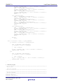
Figure 4.1 shows the transition of RUN mode and power-save modes.
Reset
AWO
ISO
Reset release
RUN
AWO
ISO
STBC0PSC.STBC0DISTRG = 1
STBC0STPT.STBC0STPTRG = 1
Wake-up factor 1
*2
occurred
Wake-up factor 1
occurred
STOP
AWO
*1
DEEPSTOP
ISO
AWO
HALT instruction
executed
Interrupt occurred
Wake-up factor 2
occurred
ISO
STBC0PSC.STBC0DISTRG = 1
Wake-up factor 1 occurred
HALT
AWO
Power Domain configuration
Cyclic RUN
ISO
HALT instruction executed
AWO
STBC0STPT.STBC0STPTRG = 1
Powered
ISO
Wake-up factor 1 or 2
occurred
Cyclic STOP
Not powered
AWO
ISO
Notes: 1. Set MainOsc or high-speed IntOsc as the CPU clock source.
2. To return from DEEPSTOP to RUN, ISO peripheral function registers must be set anew.
Figure 4.1 State transition diagram of stand-by mode
4.1
Overview
Table 4.1 lists the definition and mode transition trigger of the operation modes:
R01AN1877ED0100 Rev.1.00
Dec. 23, 2013
Page 9 of 82
RH850/F1x
Low-Power Operations
Table 4.1 List of operation modes
Operation Mode
Definition
1
RUN*
All functions are operational
CPU operation stopped
all clocks operation except clock for
CPU core continue
all areas are under power
Several clock supplies are stopped
HALT
STOP
DEEPSTOP
Power supply of ISO area is turned off
CPU clock is 8MHz HS-IntOSC or
MainOSC
instruction fetch from retention RAM
Cyclic STOP
All functions stopped
MOSC and RLIN3 still operating
Low-Power Sampler for cyclic
CPU operation stopped
2
wake-up*
Port polling and A/D conversion
executed by low-power sampler
Notes: 1. The RUN mode is not discussed in this application note.
Cyclic RUN
Mode Transition Trigger
HALT instruction
Register
Register
Wake-up factor (AWO
interrupts)
Register
TAUJ interrupt
2. For detailed information of low-power sampler, please see section 6.
4.2
Details
4.2.1
HALT Mode
During HALT mode the CPU operation and the clock supply to CPU core are stopped, while clocks sources and
peripherals (except ICU-S) continue to operate and all areas are under power.
HALT mode affects neither power domains nor clock domain.
According to Figure 4.1, the device can be transferred to HALT mode by HALT instruction executed on CPU.
The HALT state can be terminated and the device returns to RUN mode, after any interrupt requests and exceptions
such as debugging interrupts and relay breaks have been accepted.
Table 4.2 lists the operation status of the HALT mode.
Table 4.2 Operation status of HALT mode
Function
Port
AWO
ISO
CPU core
DMA
Interrupt Controller (INTC)
External Memory Controller (MEMC)
External Interrupt
R01AN1877ED0100 Rev.1.00
Dec. 23, 2013
HALT Mode
Port: Operable
Pin: Operable
Port: Operable
Pin: Operable
Stop
Operable
Operable
Stop
Operable
Page 10 of 82
RH850/F1x
ICU-S
Power
Clock
Memory
Timer
Communication
*2
Safety
A/D Converter
Key Return
Low-Power Operations
AWO
ISO
Main Oscillator
Sub Oscillator
High Speed Internal Oscillator (HS IntOsc)
Low Speed Internal Oscillator (LS IntOsc)
PLL0
CPUCLK
Code Flash
Data Flash
Local RAM (Primary)
Local RAM (Secondary)
Retention RAM
Operating System Timer (OSTM)
Window Watchdog Timer (WDTA0)
Window Watchdog Timer (WDTA1)
Timer Array Unit D (TAUD)
Timer Array Unit B (TAUB)
Timer Array Unit J0 (TAUJ0)
*1
Timer Array Unit J1 (TAUJ1)
Real-time Counter (RTCA)
Motor Control
Encoder Timer (ENCA)
PWM Diagnostic (PWM-Diag)
RLIN3
RLIN2
CSIG
CSIH
I2C Interface (RIIC)
CAN Interface (RS-CAN)
CLMA0
CLMA1
CLMA2
Data CRC (DCRA)
Core Voltage Monitor (CVM)
Power-On Clear (POC)
Low-Voltage Indicator (LVI)
AD-Converter (ADCA0)
*1
AD-Converter (ADCA1)
Key return (KR)
Stop
Power on
Power on
Oscillation enabled
Oscillation continues
Oscillation continues
Oscillation continues
Operable
Run
Operable
Operable
Operable
Operable
Operable
Operable
Operable
Operable
Operable
Operable
Operable
Operable
Operable
Operable
Operable
Operable
Operable
Operable
Operable
Operable
Operable
Operable
Operable
Operable
Operable
Operable
Operable
Operable
Operable
Operable
Operable
Operable
Notes: 1. The functions in this table are related to RH850/F1L 176-pin device, for other RH850/F1L devices
please refer to Hardware User’s Manual R01UH0390EJxxxx.
2. For the devices which support Temperature Sensor (TMPS), the TMPS is operable in HALT mode.
4.2.2
STOP Mode
In STOP mode, the clock supply to CPU ore and CPU subsystem is stopped. The PLL operation is stopped, while the
other clock sources can operate. In addition, all the related peripheral functions are stopped before the transition to
STOP mode is made.
R01AN1877ED0100 Rev.1.00
Dec. 23, 2013
Page 11 of 82
RH850/F1x
Low-Power Operations
The contents of local RAM and retention RAM before the transition to STOP mode are remained. Limited peripherals
on AWO and ISO area can operate.
The I/O buffers of areas in STOP mode (clock has been stopped) remain in the state before entering STOP mode (I/O
buffer hold state is not entered).
Before starting STOP or DEEPSTOP mode, the following setup is needed as the preparation for stand-by:
Stop all of the peripheral functions to which the clock supply is to be stopped.
Disable the interrupt handling by the CPU instruction “DI”.
Set the interrupt control registers.
Set the RFxxx bit of EI Level Interrupt Control register ICxxx to 0, clear the interrupt request flag.
Set the MKxxx bit of the corresponding EI Level Interrupt Control register ICxxx.
To mask the interrupt of non-wake-up factor, this bit must be set to 1; to release the interrupt of wake-up factor,
this bit must be set to 0.
Set the wake-up related registers.
Clear the wake-up factor flag by using the Wake-Up Factor Clear registers WUFC0 and WUFC_ISO0.
Configure the corresponding bit of the Wake-Up Factor Mask registers WUFMSK0 and WUFMSK_ISO0: set 1
to disable the wake-up event; set 0 to enable wake-up event.
Set the clock source related registers:
Set the xxxxSTPMSK bit of the corresponding Stop Mask registers CKSC_xxx_STPM.
To remain the clock domain of a macro in stand-by mode, this bit must be set to 1; to stop the clock domain of a
macro, this bit must be set to 0.
Designate each clock source for oscillation or for stopping. Configure the Stop Mask register MOSCSTPM for
MainOsc and ROSCSTPM for HS IntOsc to set the clock mask and select the clock source to be stopped or to
continue operation.
For MOSCSTPM.MOSCSTPMSK =1 or ROSCSTPM.ROSCSTPMSK=1, the STOP request signal is
masked, the corresponding clock source continues to operate in stand-by.
For MOSCSTPM.MOSCSTPMSK =0 or ROSCSTPM.ROSCSTPMSK=0, The STOP request signal is not
masked, the clock source is stopped in stand-by. It is automatically restarted after wake-up from stand-by if
was in operation before stand-by.
According to Figure 4.1, to shift the device into STOP mode, the STBC0STPT.STBC0STPTRG bit is set to 1.
The device can return to RUN mode from STOP mode, when a wake-up event is generated as configured in the
corresponding WUF register.
For the detailed information for the operation status of STOP mode, please refer to Table 4.3 in section 4.2.3.
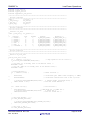
The transition procedure (example) to STOP mode is shown below in Figure 4.2.
R01AN1877ED0100 Rev.1.00
Dec. 23, 2013
Page 12 of 82
RH850/F1x
Low-Power Operations
RUN mode
STOP mode
Wake-up event*4
Stop all of the peripheral
functions to which the clock
supply is to be stopped*1
Interrupt enabled (EI)
Interrupt prohibited (DI)
Clear all interrupt flags
Interrupt processing
Clear all of the wake-up factors
and mask the wake-up
Interrupt handling*5
Mask the clock domain and the
source clock*2
Set STBC0STPT = 01H
RUN mode
Read STBC0STPT
Set STBC0STPT = 01H?
Yes
STOP mode*3
Notes: 1. Before the transition to STOP mode, all the peripheral functions whose clock supply will be
stopped, must be turned off. Otherwise the operation of the peripheral function may be incorrect.
2. The clock mask must be set before 01H is written to STBC0STPT.
3. The clock supply to the CPU is stopped and the operation shifts to the STOP mode while checking
that STBC0STPT = 01H.
4. STBC0STPT is set to 00H at the generation of a wake-up event. The generated wake-up event can
be checked by the WUF0 and WUF_ISO0 registers.
R01AN1877ED0100 Rev.1.00
Dec. 23, 2013
Page 13 of 82
RH850/F1x
Low-Power Operations
5. This processing is optional. It is required to execute the interrupt handling after the wake-up.
Figure 4.2 Example of STOP mode transition
4.2.3
DEEPSTOP Mode
In DEEPSTOP mode, the clock supply to all areas and the power supply to the Isolated Area are stopped. Select the
clock other than the PLL as the CPU operating clock, before the transition to DEEPSTOP mode is made.
The I/O buffers in DEEPSTOP mode are changing into I/O buffer hold state by default, i.e. the state of the buffer is
frozen. The input or output remains in the state before entering DEEPSTOP mode, no external or internal signal can
change its state until the I/O buffer hold state is terminated.
The preparation of DEEPSTOP mode is described in section 4.2.2.
According to Figure 4.1, if the STBC0PSC.STBC0DISTRG bit is set to 1, the device starts DEEPSTOP mode.
If a wake-up event is generated, the microcontroller returns from DEEPSTOP mode to RUN mode or Cyclic RUN
mode:
The wake-up factor 1 is determined by the wake-up factor flag WUF0 and WUF_ISO0.If a wake-up factor 1 is
detected, the device returns from DEEPSTOP mode to RUN mode, and the operation is started from the reset
address.
If a wake-up factor 2 is detected during DEEPSTOP mode, the device is transferred to Cyclic RUN mode.
The wake-up factor 1 is determined by the wake-up factor flag WUF0 and WUF_ISO0.
The wake-up factor 2 is determined by the wake-up factor flag WUF20.
If wake-up factor occurs, the ports in the isolated area maintain the I/O buffer hold state.
Release the hold state of I/O buffer in the following order.
Re-configure the peripheral functions and port functions.
IOHOLD.IOHOLD = 0
To execute an interrupt of the wake-up factor after the wake-up, evaluate the information of wake-up factor flag by
software and set the interrupt request flag in the interrupt control register. When an interrupt is enabled by the CPU
instruction “EI”, the generated wake-up interrupt is to be executed.
For the detailed information for the operation status of DEEPSTOP mode, please refer to table 4.3.
Table 4.3 Operation statuses of STOP and DEEPSTOP modes
Function
Port
AWO
ISO
CPU core
DMA
Interrupt Controller (INTC)
External Memory Controller (MEMC)
External Interrupt
R01AN1877ED0100 Rev.1.00
Dec. 23, 2013
STOP Mode
DEEPSTOP Mode
Port: State before STOP/DEEPSTOP mode was set is
retained
Pin: Operable
Port: State before STOP
Port: Power off
mode was set is retained
Pin: State before
Pin: Operable
DEEPSTOP mode was
set is retained
Stop
Power off
Stop
Power off
Stop
Power off
Stop
Power off
Operable
Operable for wake-up
Page 14 of 82
RH850/F1x
ICU-S
Power
Clock
Memory
Low-Power Operations
AWO
ISO
Main Oscillator
Sub Oscillator
High Speed Internal
Oscillator (HS IntOsc)
Low Speed Internal
Oscillator (LS IntOsc)
PLL0
CPUCLK
Code Flash
Data Flash
Local RAM (Primary)
Local RAM (Secondary)
Timer
Communication
*2
Safety
Retention RAM
Operating System Timer
(OSTM)
Window Watchdog Timer
(WDTA0)
Window Watchdog Timer
(WDTA1)
Timer Array Unit D
(TAUD)
Timer Array Unit B
(TAUB)
Timer Array Unit J0
(TAUJ0)
Timer Array Unit J1
*1
(TAUJ1)
Real-time Counter
(RTCA)
Motor Control
Encoder Timer (ENCA)
PWM Diagnostic (PWMDiag)
RLIN3
RLIN2
CSIG
CSIH
I2C Interface (RIIC)
CAN Interface (RS-CAN)
CLMA0
CLMA1
CLMA2
Data CRC (DCRA)
Core Voltage Monitor
(CVM)
Power-On Clear (POC)
Low-Voltage Indicator
(LVI)
R01AN1877ED0100 Rev.1.00
Dec. 23, 2013
Stop
Power on
Power on
Oscillation enabled
Oscillation continues
Oscillation enabled
Power off
Power on
Power off
Oscillation continues
Stop
Power off
Stop
Power off
Stop
Power off
Stop
Power off
State before STOP mode was Power off
set is retained
State before STOP mode was Power off
set is retained
State before STOP/DEEPSTOP mode was set is retained
STOP
Power off
Operable
Operable
Operable
Power off
STOP
Power off
STOP
Power off
Operable
Operable
STOP
Power off
Operable
Operable
STOP
STOP
STOP
Power off
Power off
Power off
Setting prohibited
Setting prohibited
STOP
STOP
STOP
Operable
Operable
Operable
STOP
STOP
STOP
Power off
Power off
Power off
Power off
Power off
Power off
Operable
Operable
Power off
Power off
STOP
Operable
Operable
Operable
Operable
Page 15 of 82
RH850/F1x
A/D Converter
Key Return
Low-Power Operations
AD-Converter (ADCA0)
*1
AD-Converter (ADCA1)
Key return (KR)
Setting prohibited
STOP
Operable
STOP
Power off
Power off
Notes: 1. The functions in this table are related to RH850/F1L 176-pin device, for other RH850/F1L devices
please refer to Hardware User’s Manual R01UH0390EJxxxx.
2. For the devices which support Temperature Sensor (TMPS), the TMPS is not operable in STOP
and DEEPSTOP mode.
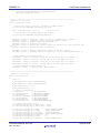
The transition procedure (example) to DEEPSTOP mode is shown below in Figure 4.2.
RUN mode
DEEPSTOP mode
Wake-up event*3
Stop all of the peripheral
functions to which the clock
supply is to be stopped*1
Check registers RESF, WUF0, and
WUF_ISO0
Interrupt prohibited (DI)
Port resetting in the ISO area
Clear all interrupt flags
Cancel the input/output hold
(IOHOLD = 0)
Clear all of the wake-up factors
and mask the wake-up
Interrupt enabled (EI)
Clear the RESF register
Set STBC0PSC = 02H*2
Interrupt processing
Interrupt handling*4
DEEPSTOP mode*2
R01AN1877ED0100 Rev.1.00
Dec. 23, 2013
RUN mode
Page 16 of 82
RH850/F1x
Low-Power Operations
Notes: 1. When the operation of the peripheral function is stopped during operating due to the transition to
the DEEPSTOP mode, the operation of the peripheral function may be incorrect. Therefore, before
the transition to the DEEPSTOP mode, all of the peripheral functions whose clock supply is to be
cut off, must be stopped.
2. After setting STBC0PSC = 02H, wait for the transition to the DEEPSTOP mode by the
unconditional loop.
3. The CPU starts the program from the reset vector after the generation of a wake-up event. The
return from the DEEPSTOP mode by a reset can be checked by the RESF register. In addition,
the generated wake-up event can be checked by the WUF0 and WUF_ISO0 registers.
4. This processing is optional. It is required to execute the interrupt handling after the wake-up.
Figure 4.3 Example of DEEPSTOP mode transition
4.2.4
Cyclic RUN and Cyclic STOP Mode
In Cyclic RUN mode, the functions except the CPU, AWO area peripheral function and RLIN3 are stopped.
In Cyclic STOP mode, the functions except the AWO area peripheral function and RLIN3 are stopped.
Before the transition to Cyclic RUN mode, the following preparation is necessary.
Set up interval timer (TAUJ0) to serve as periodic wake-up trigger.
Arrange the program for Cyclic RUN in the Retention RAM.
Set the wake-up related registers.
Clear the wake-up factor flag by writing 1 to the register WUFC20.
Configure the corresponding bit of the WUGMSK20 register: set 1 to disable the wake-up event; set 0 to enable
wake-up event.
Make the transition to DEEPSTOP mode. For details on how to transit to DEEPSTOP mode, please refer to Section
4.2.3, DEEPSTOP mode.
As is structured in Figure 4.1, the operation shifts to Cyclic RUN mode from DEEPSTOP at the generation of wake-up
factor 2, which is determined by the wake-up factor flag in register WUF20.
And the Cyclic RUN mode ends at the transition to the STOP mode by setting the STBC0STPT.STBC0STPTRG bit to
1, or the shift to the DEEPSTOP mode by setting the STBC0PSC.STBC0DISTRG bit to 1.
Table 4.4 lists the detailed operation status of Cyclic RUN mode.
Table 4.4 Operation Statuses of Cyclic RUN and Cyclic STOP modes
Function
Port
AWO
ISO
CPU core
DMA
R01AN1877ED0100 Rev.1.00
Dec. 23, 2013
Cyclic RUN Mode
Port: Operable
Pin: Operable
Port: Operable
Pin: Operable
Instruction execution from
retention RAM
Setting prohibited
Cyclic STOP Mode
Port: State before Cyclic
STOP mode was set is
retained
Pin: Operable
Port: Power off
Pin: State before Cyclic
STOP mode was set is
retained
Stop
Stop
Page 17 of 82
RH850/F1x
Low-Power Operations
Interrupt Controller (INTC)
External Memory Controller (MEMC)
External Interrupt
ICU-S
Power
AWO
ISO
Clock
Main Oscillator
Sub Oscillator
High Speed Internal
Oscillator (HS IntOsc)
Low Speed Internal
Oscillator (LS IntOsc)
PLL0
CPUCLK
Memory
Code Flash
Data Flash
Local RAM (Primary)
Local RAM (Secondary)
Retention RAM
Operable
Setting prohibited
Operable
Setting prohibited
Power on
Power on
Oscillation enabled
Oscillation continues
Oscillation enabled
Timer
Setting prohibited
Setting prohibited
Stop
Stop
Stop
Stop
Stop
State before Cyclic STOP
mode was set is retained
Setting prohibited
Operable
Stop or operation continues
STOP
STOP
Setting prohibited
Setting prohibited
Setting prohibited
Setting prohibited
Operable
Stop or operation continues
Setting prohibited
STOP
Operable
Stop or operation continues
Setting prohibited
Setting prohibited
Setting prohibited
Setting prohibited
Setting prohibited
Setting prohibited
Operable
Setting prohibited
Setting prohibited
Setting prohibited
Setting prohibited
Setting prohibited
Operable
Operable
Setting prohibited
Setting prohibited
Setting prohibited
Stop or operation continues
Setting prohibited
Setting prohibited
Setting prohibited
Setting prohibited
Setting prohibited
Operable
Operable
Setting prohibited
Setting prohibited
Setting prohibited
Operable
Operable
Communication
*2
Safety
Operating System Timer
(OSTM)
Window Watchdog Timer
(WDTA0)
Window Watchdog Timer
(WDTA1)
Timer Array Unit D
(TAUD)
Timer Array Unit B
(TAUB)
Timer Array Unit J0
(TAUJ0)
Timer Array Unit J1
*1
(TAUJ1)
Real-time Counter
(RTCA)
Motor Control
Encoder Timer (ENCA)
PWM Diagnostic (PWMDiag)
RLIN3
RLIN2
CSIG
CSIH
I2C Interface (RIIC)
CAN Interface (RS-CAN)
CLMA0
CLMA1
CLMA2
Data CRC (DCRA)
Core Voltage Monitor
(CVM)
Power-On Clear (POC)
R01AN1877ED0100 Rev.1.00
Dec. 23, 2013
Stop
Stop
Operable
Stop
Power on
Power off
Stop or oscillation continues
Setting prohibited
Oscillation continues
Setting prohibited
Run
Access prohibited
Access prohibited
Access prohibited
Access prohibited
Operable
Page 18 of 82
RH850/F1x
A/D Converter
Key Return
Low-Power Operations
Low-Voltage Indicator
(LVI)
AD-Converter (ADCA0)
*1
AD-Converter (ADCA1)
Key return (KR)
Operable
Operable
Operable
Setting prohibited
Setting prohibited
Operable
Setting prohibited
Setting prohibited
Notes: 1. The functions in this table are related to RH850/F1L 176-pin device, for other RH850/F1L devices
please refer to Hardware User’s Manual R01UH0390EJxxxx.
2. For the devices which support Temperature Sensor (TMPS), the TMPS is not operable in Cyclic
RUN and Cyclic STOP mode.
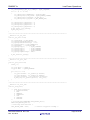
The transition procedure (example) to Cyclic RUN mode is shown below in Figure 4.4.
RUN mode
Allocate the program on the
retention RAM*1
Set wake-up factor 2 and make a
transition to the DEEPSTOP
mode*2
DEEPSTOP mode
Wake-up event*3
Check the WUF20 register
Cyclic RUN mode
Notes: 1. When the mode shifts from the Cyclic RUN mode to the RUN mode by a wake-up event, it is via
DEEPSTOP mode. The transition to the DEEPSTOP mode should be made in the processing of
the interrupt vector for the wake-up event. In that case, the interrupt processing program on the
retention RAM must be allocated.
2. Before the transition to the DEEPSTOP mode, clear the fag for wake-up factor 2 in the WUFC20
register and set wake-up factor 2 that is to be used by the WUFMSK20 register. All the other
processing for the transition to the DEEPSTOP mode is as usual.
3. The CPU starts the program from the top address on the retention RAM after the generation of a
wake-up event. The generated wake-up event can be checked by the WUF20 register.
Figure 4.4 Example of Cyclic RUN mode transition
R01AN1877ED0100 Rev.1.00
Dec. 23, 2013
Page 19 of 82
RH850/F1x
Low-Power Operations
For Cyclic STOP mode, the following setups must be done before the transition.
The transition to Cyclic RUN mode must be finished.
Set the wake-up related registers.
Clear the wake-up factor flag of the register WUFC20.
Configure the corresponding bit of the WUGMSK20 register: set 1 to disable the wake-up event; set 0 to enable
wake-up event.
Referring to Figure 4.1, the operation shifts to Cyclic STOP mode when STBC0STPT.STBC0STPTR bit is set to 1.
The Cyclic STOP mode ends and switches to the Cyclic RUN mode at the generation of wake-up factor 1 or 2.
The transition procedure (example) to Cyclic STOP mode is shown below in Figure 4.5.
Cyclic RUN mode
Set wake-up factors 1 and 2
and make a transition to STOP
mode*1
Cyclic STOP mode
Wake-up event*2
Check the WUF0, WUF20, and
WUF_ISO0 registers
Cyclic STOP mode
Cyclic RUN mode
Notes: 1. The wake-up factors 1 and 2 are set to make a transition to RUN mode and Cyclic RUN mode,
respectively. When the mode shifts to RUN mode by wake-up factor 1, the transition processing to
DEEPSTOP mode should be added in Cyclic RUN mode.
2. When a wake-up factor is generated in Cyclic STOP mode, the mode shifts to Cyclic RUN mode
and the operation starts immediately after the processing shifted to Cyclic STOP mode. The
generated wake-up factors can be checked by the WUF0, WUF20, and WUF_ISO0 registers.
Figure 4.5 Example of Cyclic STOP mode transition
4.3
Wake-up Factors
For different mode transition, the device provides different category of wake-up events. Table 4.5 shows an overview of
these wake-up factors and the operation after wake-up events.
Table 4.5 Overview of Wake-up Factors
Category
Mode Transiton
Wake-up Factor
Interrupt
HALT→RUN
All interrupt
factors
Wake-up 1
STOP→RUN
All wake-up
R01AN1877ED0100 Rev.1.00
Dec. 23, 2013
Operation after Wake-up
CPU Clock
Fetch Address
Clock setting before
Next address before HALT
HALT mode
mode was entered or
interrupt vector
Clock setting before
Next address before STOP
Page 20 of 82
RH850/F1x
Low-Power Operations
factors
Wake-up 2
RESET
STOP mode
DEEPSTOP→
Wake-up factors
RUN
of AWO area
Cyclic
All wake-up
RUN/STOP→
factors
RUN
DEEPSTOP→ Wake-up 2 factors
Cyclic RUN
of AWO area
Cyclic
All wake-up 2
STOP→Cyclic
factors
RUN
All states to
All RESET factors
RESET to RUN
Emergency Clock (8
MHz or 240 kHz)
Emergency Clock (8
MHz or 240 kHz)
Emergency Clock (8
MHz or 240 kHz)
Emergency Clock (8
MHz or 240 kHz)
Emergency Clock (8
MHz or 240 kHz)
mode was entered or
interrupt vector
RESET vector of code flash
RESET vector of code flash
RESET vector of retention
RAM
Next address before Cyclic
STOP mode was entered or
interrupt vector
RESET vector of code flash
The wake-up events for terminating a power save mode are controlled and monitored by the following Stand-by
Controller registers:
Wake-Up Mask registers: WUFMSK0, WUFMSK20, WUFMSK_ISO0
Each bit of these registers is assigned to a certain wake-up event. Wake-up by this event is enabled if the
corresponding mask bit is set to 0. Wake-up factor assigned to Wake-up factor 1 and 2 should not to be enabled at
the same mode.
Wake-Up Factor registers: WUF0, WUF20, WUF_ISO0
Upon occurrence of an unmasked wake-up event, the associated wake-up factor flag is set to 1.
The application program can identify the wake-up factor by using these registers.
Wake-Up Factor Clear registers: WUFC0, WUFC20, WUFC_ISO0
In order to clear an occurred Wake-up factor flag of a Wake-up factor register (WUF0, WUF20, WUF_ISO0), the
assigned bit of the related register has to be set to 1.
The Wake-up factor flags in the Wake-up factors registers (WUF0, WUF20, WUF_ISO0) indicate only the occurrence
of a Wake-up factor. Thus an asserted Wake-up factor flag does not mean that the transition from stand-by to normal
operation mode is already accomplished.
Table 4.6 and Table 4.7 list respectively the macros, which can return from stand-by mode by the corresponding wakeup factors 1 and 2.
For the same wake-up event, only wake-up factor 1 or wake-up factor 2 can be assigned, it is invalid to use both at the
same time.
Table 4.6 Wake-up Factors 1 and Registers Assignments
Wake-up factors 1
Unit
NMI
WDTA0NMI
INTLVIL
INTP0
INTP1
INTP2
INTWDTA0
INTP3
INTP4
Port
WDTA0
LVI
Port
Port
Port
WDTA0
Port
Port
R01AN1877ED0100 Rev.1.00
Dec. 23, 2013
Bit Position by
WUFx registers
WUF0
0
WUFMS
K0
1
2
WUFC0
5
6
7
8
9
10
STOP
→RUN
√
√
√
√
√
√
√
√
√
DEEPSTOP
→RUN
√
√
√
√
√
√
√
√
√
Cyclic RUN
*1
→RUN
√
√
√
√
√
√
√
√
√
Cyclic STOP
*1
→RUN
√
√
√
√
√
√
√
√
√
Page 21 of 82
RH850/F1x
Low-Power Operations
INTP5
Port
11 √
√
√
√
INTP10
Port
12 √
√
√
√
INTP11
Port
13 √
√
√
√
WUTRG1
LPS
14 √
√
√
√
INTTAUJ0I0
TAUJ0
15 √
√
√
√
INTTAUJ0I1
TAUJ0
16 √
√
√
√
INTTAUJ0I2
TAUJ0
17 √
√
√
√
INTTAUJ0I3
TAUJ0
18 √
√
√
√
WUTRG0
LPS
19 √
√
√
√
INTP6
Port
20 √
√
√
√
INTP7
Port
21 √
√
√
√
INTP8
Port
22 √
√
√
√
INTP12
Port
23 √
√
√
√
INTP9
Port
24 √
√
√
√
INTP13
Port
25 √
√
√
√
INTP14
Port
26 √
√
√
√
INTP15
Port
27 √
√
√
√
INTRTCA01S
RTCA0
28 √
√
√
√
INTRTCA0AL
RTCA0
29 √
√
√
√
INTRTCA0R
RTCA0
30 √
√
√
√
INTDCUTDI
JTAG
31 √
√
√
√
INTKR0
KR0
WUF_IS 1
√
*2
O0
INTRCANGRECC
RS-CAN
2
√
INTRCAN0REC*2
RS-CAN WUFMS 3
√
INTRCAN1REC*2
RS-CAN
4
√
K_ISO0
*2
INTRCAN2REC
RS-CAN
5
√
WUFC_I
INTRCAN3REC*2
RS-CAN
6
√
SO0
INTRCAN4REC*2
RS-CAN
7
√
*2
INTRCAN5REC
RS-CAN
8
√
Notes: 1. Returning to RUN from Cyclic RUN and Cyclic STOP, the transition is via DEEPSTOP.
2. By using the INTP external interrupt assigned to the alternate-function pin shared with the CAN
reception pin, wake-up from DEEPSTOP is possible.
Table 4.7 Wake-up Factors 2 and Registers Assignments
Wake-up factors 2
Unit
INTADCA0I0
INTADCA0I1
INTADCA0I2
INTRLIN30
INTTAUJ0I0
INTTAUJ0I1
INTTAUJ0I2
INTTAUJ0I3
INTRLIN31
INTRLIN32
INTRTCA01S
INTRTCA0AL
INTRTCA0R
ADCA0
ADCA0
ADCA0
RLIN30
TAUJ0
TAUJ0
TAUJ0
TAUJ0
RLIN31
RLIN32
RTCA0
RTCA0
RTCA0
R01AN1877ED0100 Rev.1.00
Dec. 23, 2013
Bit Position by
WUFx registers
WUF20
0
WUFMSK20
1
2
3
4
5
6
7
8
9
10
11
12
WUFC20
DEEPSTOP → Cyclic
RUN
√
√
√
√
√
√
√
Cyclic STOP →
Cyclic RUN
√
√
√
√
√
√
√
√
√
√
√
√
√
Page 22 of 82
RH850/F1x
INTRLIN33
INTRLIN34
INTRLIN35
Low-Power Operations
RLIN33
RLIN34
RLIN35
13
14
15
-
√
√
√
For device-dependent register assignments of the wake-up factors, please refer to Hardware User’s Manual section
11.2.2.2 ‘Settings of Wake-Up Factors’.
Furthermore, a wake-up event can also be generated by the On-Chip Debug (OCD) unit, if the microcontroller runs the
application program in the following cases:
the debugger issues a stop request
a breakpoint is hit
In both cases any stand-by mode is terminated, if the OCD debug wake-up event is enabled as a wake-up factor via the
WUFMSK0 register.
In addition, it is impossible to wake-up the microcontroller from stand-by mode by a manual stop via the debugger, if
the OCD wake-up event is disabled. Thus it is recommended to enable the OCD wake-up for terminating all standby
modes by setting WUFMSK0 [31] = 0.
4.4
Configuration
Depending on a certain application with stand-by operation, the clock source and clock supply which remain in powerdown mode must be designate, using the stop mask registers (further details is discussed in section 5):
MainOsc Stop Mask register MOSCSTPM,
HS IntOsc Stop Mask register ROSCSTPM.ROSCSTPMSK,
and Stop Mask registers CKSC_xxx_STPM for corresponding macros.
If the operation includes cyclic RUN mode, retention RAM must be arranged before the transition.
To switch the microcontroller into a power-save mode, the certain registers as follows must be configured:
Registers for wake-up events:
Wake-Up Factor registers WUF0, WUF20, WUF_ISO0.
Wake-Up Factor Mask registers WUFMSK0, WUFMSK20, WUFMSK_ISO0.
Write-protected registers for power-save control:
Power-Save Control register STBC0PSC for DEEPSTOP mode.
Power Stop Trigger register STBC0STPT for STOP or cyclic STOP mode.
After a wake-up event occurred, the relevant bits of the following registers must be released:
To clear the detected wake-up factors:
Wake-Up Factor Clear registers WUFC0, WUFC20, WUFC_ISO0.
To release the I/O buffer hold state:
Write-protected register IOHOLD.
R01AN1877ED0100 Rev.1.00
Dec. 23, 2013
Page 23 of 82
RH850/F1x
5.
Low-Power Operations
Clock Controller for Low Power Configuration
For the device RH850/F1x, clock operation is able to be configured according to different peripherals in stand-by mode.
The clock supply depends on target stand-by modes and if peripheral is located on AWO or ISO area. Clock gating is
applicable for the following peripherals:
AWO
WDTA0, TAUJ0, RTCA0, ADCA0, Clock output.
ISO
WDTA1, TAUD0, TAUJ1, ENCA0, TAUB, PWM-Diag, OSTM0, RLIN3n, RLIN2, RCAN, ADCA1.
According to section 4.2.2, if a clock source or peripheral is expected to be operable in stand-by mode, the following
configuration is necessary:
Select the clock source to be stopped or to continue. Configure the Stop Mask registers MOSCSTPM and
ROSCSTPM.
If the mask bit is set to 1, the STOP request signal is masked. The corresponding clock source continues to
operate in stand-by.
If the mask bit is 0, The STOP request signal is not masked. The clock source is stopped in stand-by. It is
automatically restarted after wake-up from stand-by if was in operation before stand-by.
Configure the Clock Divider registers CKSC_xxx_CTL for the related peripherals.
Configure the Stop Mask registers CKSC_xxx_STPM for clock divider.
If the mask bit is set to 1, the corresponding clock divider continues to operate in stand-by mode.
If the mask bit is 0, the clock divider is stopped in stand-by mode.
R01AN1877ED0100 Rev.1.00
Dec. 23, 2013
Page 24 of 82
RH850/F1x
6.
6.1
Low-Power Operations
Low-Power Sampler (LPS)
Overview
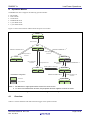
Low-power sampler provides a possibility for lowest power consumption of periodic input polling application, which
uses only macros of AWO area, and doesn’t require the CPU interaction.
To supervise the external input without consuming CPU resources, the low-power sampler (LPS) can check the digital
input ports and analog input ports without the CPU.
Each RH850/F1L 48-pin, 64-pin, 80-pin, 100-pin, 144pin and 176-pin device contents a low-power sampler, including
different channel configurations as is shown in Table 6.1.
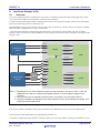
A complete LPS application is related to the following macros: LPS, ADCA0, TAUJ, STBC and clock controller.
Figure 6.1 shows a connection example (RH850/F1L 176-pin device) between the main components of the LPS and the
external circuit.
ADCA0I0
Analog Signal
Source
INTADCA0I0
ADCA0I1
ADCA0
...
ADCA0I15
INTADCA0I1
INTADCA0I2
activate
STBC
SEQADTRG
WUTRG0
APO
WUTRG1
DPO
INTCWEND
DPSEL0
DPSEL1
DPSEL2
LPS
DPIN0
activate
Digital Signal
Source
...
MUX
DPIN7
...
DPIN11
...
INTTAUJ0I0
INTTAUJ0I1
INTTAUJ0I2
TAUJ0
INTTAUJ0I3
DPIN23
Notes: 1. SEQADTRG is one of the Hardware triggers for A/D conversion. The APO is set to 1, after the
stabilization time which is configured by register CNTVAL, the LPS outputs a trigger to A/D
converter.
2. When the port input is acquired for the first time in a operation cycle, the DPO is set to 1.
3. DPSEL2 to DPSEL0 are assigned to the same alternate-function pins as DPIN10 to DPIN8. Thus
cannot be used simultaneously.
Figure 6.1 Block Diagram of the LPS
This section contains a description of the generic functions and configuration for the Low-Power Sampler (LPS).
In this section, the individual LPS units are identified by the index “n”.
The number of digital port input channels for LPS port polling, as well as the number of analog input channels for A/D
R01AN1877ED0100 Rev.1.00
Dec. 23, 2013
Page 25 of 82
RH850/F1x
Low-Power Operations
converter, is indicated by the index “m”.
The external multiplexer select output signal for digital port is indicated by the index “k”.
LPS sequence start trigger input signal is indicated by the index “x”.
For RH850/F1L devices, n = 0, k = 0 to 2 (for 48-Pin devices, k is not defined), x = 0 to 3. The index “m” is devicedependent, the detailed information is listed in the following Table.
Table 6.1 LPS Channels of RH850/F1L Devices
Channel Name
RH850/F1L Devices
48-PIN
64-PIN
80-PIN
100-PIN
144-PIN
176-PIN
Digital Port Input DPINm
3 Ch
8 Ch
12 Ch
17 Ch
24 Ch
24 Ch
Analog Port Input ADCA0Im
8 Ch
10 Ch
11 Ch
16 Ch
16 Ch
16 Ch
6.2
Operation Modes
A LPS operation is started by interval timer TAUJ0 by AWO area, and ended by the wake-up factors or sequencer end.
During the operation, the external events are checked periodically. There are 3 operation modes:
digital mode
analog mode
mixed mode
6.2.1
Digital mode
According to Figure 6.1, the digital input ports DPINm are connected to the digital source. Port DPSELk is used to
switch the external multiplexer (optional). The DPSELk output is switched for the number of times specified in the
SCTLR register.
If the low-power sampler is set to digital mode, and the operation is triggered by the interval set of TAUJ0, the port
check is then executed after the stabilization time as is set in register CNTVAL. The operation continues regardless
whether the mode is the RUN mode or power-save mode.
When the HS IntOSC stops in stand-by mode, the operation of the HS IntOSC will be resumed while the sequencer is
running.
R01AN1877ED0100 Rev.1.00
Dec. 23, 2013
Page 26 of 82
RH850/F1x
Low-Power Operations
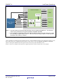
Low Power Sampler
DPO
WUTRG0
INTCWEND
DPSEL0
STBC
Event flag
DPSEL1
DPSEL2
DPIN0
activate
Digital Signal
Source
...
MUX
DPIN7
DPIN11
INTTAUJ0I1
Comparator
...
...
INTTAUJ0I0
Reference
value
Input value
INTTAUJ0I2
TAUJ0
INTTAUJ0I3
DPIN23
Notes: 1. The input values are stored in DPIN data input monitor registers DPDIMR0 to 7. The reference
value is set by DPIN data set registers DPDSR0, DPDSRM, DPDSRH.
2. The comparator compares the input value and the reference value, if the both values don’t match,
the event flag of register EVFR is set to 1, and the low-power sampler outputs a wake-up factor
WUTRG0 to the stand-by controller.
Figure 6.2 Block Diagram for the Digital mode of LPS (176-pin device)
At the completion of checking all ports that have been set, an INTCWEND interrupt occurs. Referring to Figure 6.2, the
input value of the port is compared with the reference value, which is set by the DPDSR0, DPDSRM, or DPDSRH
register. If the input is different from the expected value, the wake-up factor WUTRG0 occurs.
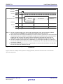
Figure 6.3 shows an example of the operation in digital input mode, when the input value is not changed.
R01AN1877ED0100 Rev.1.00
Dec. 23, 2013
Page 27 of 82
RH850/F1x
Low-Power Operations
SCTLR.DPEN
INTTAUJ0Ix
HS IntOSC
DPO
Stabilization time
SELDP[2:0]
001B 010B
000B
DPDSR0
a
DPDIMR1
b
111B
000B
a
b
...
...
DPDIMR7
h
DPDSR0
h
a
DPDSRM
edcb
DPDSRH
hgf
INTCWEND
WUTRG0
CPU
DEEPSTOP
1
2
3
4
5
6
Notes: 1. Set the SCTLR.DPEN bit to 1 by software to enable the digital input mode of the LPS.
2. When the INTTAUJ0Ix interrupt specified by the SCTLR.TJS bit is generated, the LPS enables the
HS IntOSC to start the oscillation, and outputs the high level from the DPO pin and waits for the
time specified by CNTVAL[7:0] to secure the stabilization of the external digital signal source.
3. After the completion of the signal source stabilization, the LPS stores the DPIN[7:0] input value to
the DPDIMR0 register and increments the SELDP[2:0] pins to switch the external multiplexer.
4. After the switching of the SELDP[2:0] pins, the sequencer sequentially stores the value to the
DPDIMR1 register and later and continues to increment the SELDP[2:0] pins.
5. After the value is stored up to the DPDIMR7 register, the INTCWEND interrupt is generated and
the value is compared with the expected value set in the DPDSR0, DPDSRM, and DPDSRH
registers.
6. When the value is not different from the expected value, the wake-up factor WRUTR0 is not
generated. The LPS stops the DPO output and returns to the waiting state for the trigger.
Figure 6.3 Operation of Digital Input Mode when the Input Value is not Changed (RUN Mode)
If the input value is changed, Figure 6.4 shows an example of the operation in this case.
R01AN1877ED0100 Rev.1.00
Dec. 23, 2013
Page 28 of 82
RH850/F1x
Low-Power Operations
SCTLR.DPEN
INTTAUJ0Ix
HS IntOSC
DPO
Stabilization time
DPDIMR0
a
DPDSR0
a
b
INTCWEND
WUTRG0
CPU
RUN
DEEPSTOP
1
2
3
RUN
4
5
6
Notes: 1. Set the STBC0PSC.STBC0DISTRG bit to 1 to shift to the DEEPSTOP mode, while the
SCTLR.DPEN bit is set to 1 by software to enable the digital input mode of the LPS.
2. When the INTTAUJ0Ix interrupt specified by the SCTLR.TJS bit is generated, the LPS enables the
HS IntOSC to start the oscillation.
3. After the completion of the HS IntOSC stabilization time, the LPS outputs the high level from the
DPO pin and waits for the time specified by CNTVAL[7:0] to secure the stabilization of the external
digital signal source.
4. After the completion of the signal source stabilization, the LPS stores the DPIN[23:0] input value to
the DPDIMR0 register and the INTCWEND interrupt is generated.
5. The value stored in the DPDIMR0 register is compared with the expected value set in the
DPDSR0 register. When the value is different from the expected value, the wake-up factor
WUTRG0 is generated.
6. The CPU returns to RUN mode at the generation of WUTRG0. The DPO pin is driven high until the
EVFR.DINEVF bit is cleared to 0 by software.
Figure 6.4 Operation of Digital Input Mode when the Input Value is Changed (DEEPSTOP Mode)
An overview of the LPS digital operation is illustrated in Figure 6.7 as a basic flow chart.
6.2.2
Analog Mode
In analog mode by LPS, the analog input ports which are connected to the analog source can be supervised.
After the operation is triggered by the interval set of TAUJ0, the port check is executed. The APO is set to 1, and the
LPS outputs an A/D conversion trigger to the ADCA0 after the stabilization time. The operation continues regardless
whether the mode is the RUN mode or power-save mode. When the HS IntOSC stops in stand-by mode, the operation
of the HS IntOSC will be resumed while the sequencer is running. Thus no other clock source is allowed for ADC0 as
LPS can only control HS IntOSC in stand-by mode.
The analog input is converted in ADCA0, and the conversion result is compared with the ADCA0 upper/lower. If the
input signal is not in the expected voltage range, an INTADCA0ERR interrupt is generated. Meanwhile, the wake-up
factor WUTRG1 occurs.
Figure 6.5 shows an example of the operation in analog input mode, when the conversion result is within the expected
voltage range.
R01AN1877ED0100 Rev.1.00
Dec. 23, 2013
Page 29 of 82
RH850/F1x
Low-Power Operations
SCTLR.ADEN
INTTAUJ0Ix
HS IntOSC
APO
A/D converter status
Power OFF
Power ON
A/D conversion
Power OFF
Stabilization time
INTADERR
WUTRG1
CPU
DEEPSTOP
1
2
3
4
Notes: 1. Set the conversion trigger, scan group, and expected range of the A/D converter by software.
Then, set the SCTLR.ADEN bit to 1 to enable the analog input mode of the LPS.
2. When the INTTAUJ0Ix interrupt specified by the SCTLR.TJS bit is generated, the LPS enables the
HS IntOSC to start the oscillation, and outputs the high level from the APO pin at the same time it
enables the A/D converter, and waits for the time specified by CNTVAL[15:8] to secure the
stabilization of the external analog signal source. Set the stabilization time not less than 1 μs.
3. After the completion of the signal source stabilization, the LPS triggers the start of conversion to
the A/D converter and then the A/D conversion of ADCA0Im (m = 0 to 15), set in the A/D converter
scan group, is started.
4. When the INTADCA0ERR interrupt is not generated as a result of A/D conversion, the LPS halts
the A/D converter and resets the APO pin.
Figure 6.5 Operation of Analog Input Mode when the Conversion Result is within the Expected Range
(RUN Mode)
Figure 6.6 shows an example of the operation in analog input mode, when the conversion result is not within the
expected voltage range.
R01AN1877ED0100 Rev.1.00
Dec. 23, 2013
Page 30 of 82
RH850/F1x
Low-Power Operations
SCTLR.ADEN
INTTAUJ0Ix
HS IntOSC
APO
Stabilization time
A/D converter status
Power OFF
Power ON
A/D conversion
Power ON
INTADERR
WUTRG1
CPU
RUN
1
DEEPSTOP
2
3
4
5
RUN
6
Notes: 1. Set the conversion trigger, scan group, and expected range of the A/D converter by software.
Then, set the SCTLR.ADEN bit to 1 to enable the analog input mode of the LPS.
2. Set the STBC0PSC.STBC0DISTRG bit to 1 by software to shift to the DEEPSTOP mode.
3. When the INTTAUJ0Ix interrupt specified by the SCTLR.TJS bit is generated, the LPS enables the
HS IntOSC to start the oscillation.
4. After the completion of the HS IntOSC stabilization, the LPS outputs the high level from the APO
pin at the same time it enables the A/D converter, and waits for the time specified by
CNTVAL[15:8] to secure the stabilization of the external analog signal source.
5. After the completion of the signal source stabilization, the LPS triggers the start of conversion to
the A/D converter and then the A/D conversion of ADCA0Im (m = 0 to 15), set in the A/D converter
scan group, is started.
6. When the INTADCA0ERR interrupt is generated as a result of A/D conversion, the wake-up factor
WUTRG1 is generated and the CPU returns to RUN mode. The APO pin is driven high until the
upper limit/lower limit error flag of the A/D converter is cleared to 0 by software. Set the conversion
trigger, scan group, and expected range of the A/D converter by software. Then, set the
SCTLR.ADEN bit to 1 to enable the analog input mode of the LPS.
Figure 6.6 Operation of Analog Input Mode when the Conversion Result is not within the Expected
Range (DEEPSTOP Mode)
For a generic flow chart of analog operation, please refer to Figure 6.7.
6.2.3
Mixed Mode
If digital mode and analog mode are both required in an application use case, the low-power sampler operates in the
mixed mode.
Figure 6.7 illustrates the basic flow chart of the LPS mixed mode.
R01AN1877ED0100 Rev.1.00
Dec. 23, 2013
Page 31 of 82
RH850/F1x
Low-Power Operations
TAUJ0 start
DEEPSTOP mode setting
ISO area power off
Trigger: INTTAUJ0
8MHz HS IntOSC start
HS IntOSC stabilization
Digital Operation
Port Polling Execution ?
No
Analog Operation
No
Yes
A/D Conversion Execution ?
DPO = 0 → 1
(external digital sensor on)
Yes
APO = 0 → 1
(external analog sensor on)
CNT for digital mode starts
(LPS dedicated counter)
CNT for analog mode starts
(LPS dedicated counter)
CNT Compare match wait
(Stabilization Time)
CNT Compare match
CNT Compare match wait
Read DPINm
CNT Compare match
A/D Conversion starts
Not match
Compare with the expected
data in DPDSRx
Wait for conversion end
Conversion end
Match
Compare with the upper/
lower limit
Check multiple read if
external multiplexer is used
(Max. 8)
Not match
No
Match
A/D convertion stop
Yes
DPO = 1 → 0
(external digital sensor off)
APO = 1 → 0
(external analog sensor off)
End
WUTRG0
WUTRG1
Wake up
Figure 6.7 Basic Flow chart of the Mixed Mode
R01AN1877ED0100 Rev.1.00
Dec. 23, 2013
Page 32 of 82
RH850/F1x
6.3
Low-Power Operations
Configuration
This section describes the general configuration of low-power sampler and the related macros for the basic LPS
application.
6.3.1
General Configuration for LPS application
According to Figure 6.1, a LPS application is related to the following macros: low-power sampler, Stand-by controller,
TAUJ0, ADAC0 (for analog or mixed mode) and pin functions.
TAUJ0 configuration:
The low-power sampler is started by the TAUJ0 trigger. To configure a TAUJ0 channel, the TAUJ0 registers listed
below must be specified:
TAUJ0 clock domain registers:
C_AWO_TAUJ Source Clock Selection register CKSC_ATAUJS_CTL,
C_AWO_TAUJ Clock Divider register CKSC_ATAUJD_CTL.
Both of these registers are write-protected registers.
TAUJ0 Prescaler clock Selection register TAUJ0TPS.
TAUJ0 Channel Modes OS Register TAUJ0CMORm and TAUJ0 Channel Mode User Register TAUJ0CMURm,
including the following bit setups:
Bit TAUJ0CMORm.TAUJ0MD[4:0]: selection of operation mode, here the interval timer mode is selected by
setting TAUJ0MD[4:0] to 0H;
Bit TAUJ0CMORm.TAUJ0COS[1:0]: decision of the timing to update the data register TAUJ0CDRm and
status register TAUJ0CSRm;
Bit TAUJ0CMORm.TAUJ0STS[2:0]: selection of external start trigger, in this application, the software trigger
is selected by setting TAUJ0STS[2:0] to 0H;
Bit TAUJ0CMORm.TAUJ0MAS: setup of master or slave channel if synchronous channel operation is required;
Bit TAUJ0CMORm.TAUJ0CKS[1:0] and TAUJ0CMORm.TAUJ0CCS[1:0]: selection of operation and count
clock, in this application, the TAUJ0CCS[1:0] is set to 0 H to specify the selected operation clock
(TAUJ0CKS[1:0]) as count clock;
Bit TAUJ0CMURm.TAUJ0TIS[1:0]: configuration of a valid edge of input signal TAUJTTINm.
TAUJ0 simultaneous rewrite registers:
TAUJ0 channel Reload Data Enable register TAUJ0RDE,
TAUJ0 channel Reload Data Mode register TAUJ0RDM,
TAUJ0 channel Reload Data Trigger register TAUJ0RDT.
TAUJ0 output registers:
TAUJ0 channel Output Enable register TAUJ0TOE,
TAUJ0 channel Output Mode register TAUJ0TOM,
TAUJ0 channel Output Configuration register TAUJ0TOC,
TAUJ0 channel Output Level register TAUJ0TOL,
TAUJ0 channel Output register TAUJ0TO.
For debug operation, i.e. breakpoint, TAUJ0 Emulation register TAUJ0EMU.
To start TAUJ0, set the corresponding bit of TAUJ0 Channel Start Trigger register TAUJ0TS to 1.
In a LPS application, the TAUJ0 is configured as an interval timer.
For detailed further information of TAUJ functions and configuration please refer to Hardware User’s Manual
R01UH0390EJxxxx (for RH850/F1L) section 10.4.3 ‘Clock Selector Control Register’ and section 24 ‘Timer Array
Unit J’.
R01AN1877ED0100 Rev.1.00
Dec. 23, 2013
Page 33 of 82
RH850/F1x
Low-Power Operations
Pin Functions configuration:
The LPS receives the input signals, while deriving the APO, DPO and DPSEL0 to 2 signals to the analog and digital
sources. All the related pins operate in software I/O control alternative mode.
Besides, the analog source signals are output to ADCA0. The I/O pins for ADCA0 are special alternative functions,
which are permanently connected to A/D module.
Therefore, the Pin functions must be specified before the application is started. The pin configuration is discussed
respectively for digital and analog mode, referring to section 6.3.2 and 6.3.3.
LPS general configuration:
For the general LPS configuration, the start trigger must be selected, by specifying the bit TJS[1:0] of the LPS Control
Register SCTLR.
6.3.2
Digital mode
In digital mode, the source signal, as well as the multiplexer selection signals is bounded to the low-power sampler,
where the digital sensor control signal DPO is output.
Pin Functions configuration:
To enable these LPS input and output, the related pins must operate in software I/O control alternative mode, which is
enabled by setting the following 2 registers:
Port Mode Control register PMCn:
The register specifies the operation mode of the corresponding pin.
For the related bit PMCn.PMCn_m = 0, the pin is switched to port mode;
For the related bit PMCn.PMCn_m = 1, the pin is switched to alternative mode.
Port IP Control register PIPCn:
The register specifies the I/O control mode.
For PIPCn.PIPCn_m = 0, the I/O mode of the relevant pin is selected by PMn register;
For PIPCn.PIPCn_m = 1, the I/O mode is selected by the peripheral function.
In this mode, the pins operate as alternative functions. The I/O direction is selected by setting the PMn_m bit of the
PMn register:
The pin operates in alternative output mode when PMn_m = 0,
The pin operates in alternative input mode when PMn_m = 1.
Table 6.2 shows the register setups for the 5 alternative functions, which can be selected using the port function control
registers below:
PFCn: Port Function Control register,
PFCEn: Port Function Control Expansion register,
PFCEAn: Port Function Control Additional Expansion register.
Table 6.2 Alternative Mode Selection Overview
AlternativeFunction
Output Mode 1
Register
PMC
PIPC
PM
PFCAE
PFCE
PFC
1
0
0
0
0
0
R01AN1877ED0100 Rev.1.00
Dec. 23, 2013
Page 34 of 82
RH850/F1x
Low-Power Operations
Input Mode 1
1
Output Mode 2
0
Input Mode 2
1
Output Mode 3
0
Input Mode 3
1
Output Mode 4
0
Input Mode 4
1
Output Mode 5
0
Input Mode 5
1
0
0
1
0
1
0
0
1
1
1
0
0
The necessary information to enable the LPS inputs and output ports in the device RH850/F1L can be found in
Appendix A:
Table A-1 lists the corresponding port functions and pin connections.
The digital mode input and output in Table A-1 must be configured. DPSEL2 to DPSEL0 cannot be used
simultaneously with DPIN10 to DPIN8, while they are assigned to the same alternate-function pins.
LPS configuration:
To switch the LPS into digital mode, the registers listed below must be specified:
DPIN Select registers DPSEL 0, DPSELM and DPSELH.
These registers specify the ports to be employed in the application.
DPIN Data Set registers DPDSR0, DPDSRM and DPDSRH.
These registers store the data to be compared with the data in Data Input registers DPDIMR0 to 7, which acquired
the digital port input in the operation.
Count Value registers CNTVAL:
This register specifies the stabilization time of the external circuits, i.e. the time when the DPO output is set to 1 to
the time when the port input is acquired for the first time.
Bit 7 to 0 should be set for digital signal source.
The stabilization time can be calculated like this: stabilizat ion time ( 1 / HS IntOSC ) 16 set value .
The typical stabilization time of digital mode is 50µs.
LPS Control register SCTLR:
This register specifies the digital mode of the corresponding pin.
Set bit SCTLR.TJS[1:0] to select the TAUJ0 channel, referring to section 6.3.1.
Set bit SCTLR.NUMDP[2:0] with the bit position 6 to 4, to specify the number of times the port is read in digital
mode.
These bits above must be setup before the sequence operation is started, i.e. when SCTLR.DPEN = 0,
SCTLR.ADEN = 0 and SOSTR.SOF = 0.
After all the LPS configuration is finished, the bit SCTLR.DPEN with the bit position 0 can be set to 1, to enable
digital input mode.
The LPS status of digital mode can be checked in the following registers:
LPS Operation State register SOSTR.
Bit SOSTR.SOF indicates the operating state of LPS:
SOSTR.SOF = 1 means that the operation is in progress,
SOSTR.SOF = 0 means that the operation is not started.
Event Flag register EVER.
Bit EVER.DINEVF indicates the compare result of LPS:
R01AN1877ED0100 Rev.1.00
Dec. 23, 2013
Page 35 of 82
RH850/F1x
Low-Power Operations
For EVER.DINEVF = 0, the result of comparison is match,
For EVER.DINEVF = 1, the result of comparison is mismatch.
For further detailed information, please see Hardware User’s Manual R01UH0390EJ0081 (for RH850/F1L) section
12.3 ‘Registers (LPS)’.
STBC Configuration:
A LPS Application is started in DEEPSTOP mode, and if a mismatch occurs, the microcontroller switches
automatically into RUN mode from DEEPSTOP mode.
Therefore, the STBC macro must be configured as is described below:
Set the Wake-Up Factor Mask registers WUFMSK0.
The wake-up factor WUTRG0 can be enabled by setting the bit WUFMSK0[19] of this register to 0.
Start DEEPSTOP mode using the Power Save Control register STBC0PSC.
After the operation mode of the MCU is switched into RUN mode:
Clear the wake-up factor by writing 1 to the corresponding bit of the Wake-Up Factor Clear register WUFC0.
Release the I/O hold state by writing 0 to the IOHOLD register.
6.3.3
Analog Mode
In analog mode, the input signals are connected to the A/D converter, the low-power sampler outputs the APO signal
and triggers the ADCA0, and the stand-by controller receives the wake-up factor WUTRG1 and INTADCA0ERR if the
input is out of the expected voltage range.
Pin Functions configuration:
To configure the LPS output signal APO, please refer to section 6.3.2 and Table A-1 in Appendix A.
Besides, the ADCA0 inputs are Special Alternative Pins, which are permanently connected to A/D module. Thus the
ADCA0 inputs are specified by directly connecting to the corresponding pins.
The pin assignments of the ADCA0 input channels and their related configuration used in this application note are listed
in Table A-2 of Appendix A.
ADCA0 Configuration:
The following setup is required for using the ADCA0:
ADCA0 clock configuration.
The clock signal for ADCA macro is selected in the clock controller through the Source Clock Selection register
CKSC_AADCAS_CTL and Clock Divider register CKSC_AADCAD_CTL.
In this application, the HS IntOsc is selected by setting register CKSC_AADCAS_CTL 01H.
For details to write these registers in RH850/F1L device, please refer to Hardware User’s Manual
R01UH0390EJxxxx section 10.4.3 ‘Clock Selector Control Register’.
ADCA0 basic configuration with following points:
Setting of conversion method,
Selection of 10-bit or 12-bit resolution,
Selection of the conversion result alignment control,
Configurations of the upper limit/lower limits; overwrite check for data registers; read and clear function for data
registers.
Table 6.3 lists the registers and related bit positions in which the mentioned functions can be configured.
ADCA0 scan group setups:
R01AN1877ED0100 Rev.1.00
Dec. 23, 2013
Page 36 of 82
RH850/F1x
Low-Power Operations
Configuration of start and end virtual channel of the scan group;
Setting of the scan mode, scan end interrupt enable, channel repeat times;
Specification of times for scanning, if the scan mode is selected for multicycle scan mode.
For detailed information, please refer to Table 6.3.
ADCA0 trigger setups:
In a LPS application, the ADCA0 is triggered by the low-power sampler, thus a hardware trigger is required for the
A/D converter:
Select hardware trigger mode by setting 1 to bit ADCA0SGCRx.TRGMD of the Scan Group x Control register
ADCA0SGCRx,
To set the LPS SEQADTRG trigger as the start trigger of the expected scan group x, the bit TxSEL4 of the A/D
Conversion Trigger Select Control register ADCA0SGTSELx must be set to 1.
Table 6.3 ADCA0 Configuration
*2
Function
Register
Bit Name
Bit Position
10-bit or 12-bit Resolution
ADCA0ADCR
CTYP
4
Left or Right Align
CRAC
5
Suspend Mode
SUSMTD[1:0]
1, 0
RDCLRE
4
Upper/lower Limit Error Interrupt
Disable/Enable
ULEIE
3
Overwrite Error Interrupt Disable/Enable
OWEIE
2
Read and Clear Disable/Enable
ADCA0SFTCR
Sampling Time
ADCA0SMPCR
SMPT[7:0]
7 to 0
Upper Limit
ADCA0ULLMTBR0 to 2
ULMTB[11:0]
31 to 20
LLMTB[11:0]
15 to 4
Lower Limit
Scan Group x Start Virtual Channel
ADCA0SGVCSPx
VCSP[5:0]
5 to 0
Scan Group x End Virtual Channel
ADCA0SGVCEPx
VCEP[5:0]
5 to 0
ADCA0SGMCYCRx
MCYC[1:0]
1 to 0
ADCA0SGCRx
SCANMD
5
Scan End Interrupt Disable/Enable
ADIE
4
Channel Repeat Times Selection
SCT[1:0]
3 to 2
Trigger Mode
TRGMD
0
TxSEL[8:0]
8 to 0
Number of scans for Multicycle Mode
Multicycle or Continuous Scan Mode
Hardware Trigger Selection
*1
ADCA0SGSELx
Notes: 1. Setup of this register is only required if the Multicycle scan mode is selected in register
ADCA0SGCRx.
2. The setup details for RH850/F1L devices are described in Hardware User’s Manual
R01UH0390EJ0081 section 29.3 ‘Registers (ADCA)’.
LPS configuration:
To switch the LPS into analog mode, the registers listed below must be specified:
Count Value registers CNTVAL:
This register specifies the stabilization time of the external circuits, i.e. the time when the APO output is set to 1 to
the time when the LPS outputs the A/D conversion trigger to ADCA0.
Bit 15 to 8 should be set for analog signal source.
R01AN1877ED0100 Rev.1.00
Dec. 23, 2013
Page 37 of 82
RH850/F1x
Low-Power Operations
The stabilization time can be calculated like this: stabilizat ion time ( 1 / HS IntOSC ) 16 set value .
The typical stabilization time of analog mode is 100µs.
LPS Control register SCTLR:
This register specifies the digital mode of the corresponding pin.
Set bit SCTLR.TJS[1:0] to select the TAUJ0 channel, referring to section 6.3.1.
These bits must be setup before the sequence operation is started, i.e. when SCTLR.DPEN = 0, SCTLR.ADEN = 0
and SOSTR.SOF = 0.
After all the LPS configuration is finished, the bit SCTLR.ADEN with the bit position 1 can be set to 1, to
enable analog input mode.
The LPS status of analog mode can be checked in the following registers:
LPS Operation State register SOSTR.
Bit SOSTR.SOF indicates the operating state of LPS:
SOSTR.SOF = 1 means that the operation is in progress,
SOSTR.SOF = 0 means that the operation is not started.
For further detailed information, please see Hardware User’s Manual R01UH0390EJ0081 (for RH850/F1L) section
12.3 ‘Registers (LPS)’.
STBC Configuration:
For analog mode, the STBC macro configuration is described below:
Set the Wake-Up Factor Mask registers.
The wake-up factor WUTRG1 can be enabled by setting WUFMSK0[14] = 0.
If a cyclic operation is required after the A/D conversion, the wake-up factor INTADCA0Ix of the scan group x,
which is employed for the application, can be enabled by setting 0 to the bit WUFMSK20[x] of register
WUFMSK20, where x = 0 to 2.
Start DEEPSTOP mode using the Power Save Control register STBC0PSC.
After the operation mode of the MCU is switched into RUN mode:
Clear the wake-up factor by writing 1 to the corresponding bit of the Wake-Up Factor Clear register WUFC0.
Release the I/O hold state by setting 0 to the IOHOLD register.
6.3.4
Mixed Mode
According to Figure 6.7, the mixed mode is an operation mode includes both digital and analog mode. Therefore, the
configuration of mixed mode is a combination of digital and analog mode.
For details, please refer to section 6.3.2 and 6.3.3.
R01AN1877ED0100 Rev.1.00
Dec. 23, 2013
Page 38 of 82
RH850/F1x
7.
Low-Power Operations
Use Cases
This section enumerates several examples of the low power operation in common use.
7.1
Digital and Analog
To present the cyclic wake-up example application, using both digital and analog mode of LPS, the following expected
conditions are used for the setups:
Cyclic Period: 40ms;
Retention RAM: Data Hold;
AWO: Peripheral operating, using LPS, TAUJ0 and ADCA0;
ISO: Power off;
Ta: 25 ºC;
Channels: 24 digital inputs and 8 analog inputs.
The flow chart of the application is illustrated in Figure 6.7.
Figure 7.1 shows the cyclic wake-up current calculation of digital and analog inputs.
I
IO acquisition,
Digital *3
Active mode, ADCA on
Active mode
Low power mode, basic operation
Start IO supply*1
About 50µs*2
IO acquisition,
Analog *5
Start IO supply*1
About 100µs*4
Low power mode, peripherals off
40ms*6
t
Notes: 1. Refferring to Figure 6.7, the I/O supply is started when the DPO or APO is set to 1.
2. The SEQ dedicated counter starts the count for a stabilisation time of about 50 µs for digital mode.
3. After the stabilization time, the LPS starts the I/O acquisition and data comparetion; when the
compare process is ended, if there is no mismatch of the input signal, the microcontroller returns
to low power mode before the analog excution.
4. The SEQ dedicated counter starts the count for a stabilisation time of about 100 µs for analog
mode.
5. After the stabilization time, the ADCA0 starts the I/O acquisition and conversion; if the input signals
are in the expected voltage range, the microcontroller returns to low power mode before the next
operation cycle starts.
6. In the 40 ms cyclic period, the microcontroller works firstly in DEEPSTOP mode before the I/O
supply is started; and then operates in DEEPSTOP mode with LPS Operation as is described in
Note 1, 2 and 3; after the LPS operation is finished, the MCU ends the period with TAUJ0 trigger,
and remains DEEPSTOP mode for the start of next period.
Figure 7.1 Cyclic Wake-up Calculation of Digital and Analog Inputs
The configuration of the following macros is required for this example, the setup details are described in section 6.3:
R01AN1877ED0100 Rev.1.00
Dec. 23, 2013
Page 39 of 82
RH850/F1x
Low-Power Operations
Clock domain,
Pin functions,
TAUJ0 timer,
Stand-by controller,
ADCA0,
Low-power sampler.
7.2
LIN Communication
A LIN Communication application with cyclic operation provides the possibility to reduce the power consumption
during LIN communication.
The test condition of the example software in this document is set as follows:
Cyclic Period: 800ms;
Retention RAM: Data Hold;
AWO: Peripheral operating, using TAUJ0 and RLIN3;
ISO: Power off & cyclic RUN;
Ta: 25 ºC.
Figure 7.2 shows the cyclic wake-up calculation of the LIN communication example, the flow chart of which is shown
in Figure 7.3.
I
Active mode
Low power mode, LIN on
Low power mode, crystal on
Start
Send LIN
*4
crystal*1 message1*2 Stop all
Start
crystal
Send LIN Send LIN
message2*5 message3
Duration of
LIN message*3
About 4ms
Send LIN
message4
Stop all
Duration of Duration of Duration of
LIN message LIN message LIN message
About 4ms
Low power mode, peripherals off
800ms
t
Notes: 1. In the 800 ms cyclic period, the microcontroller is firstly in DEEPSTOP mode before the oscillator
is started; and switches into cyclic RUN mode once the interval timer TAUJ0 (ch1, refer to Figure
7.3) triggers.
2. In Cyclic RUN mode, the LIN communication is excuted; after the LIN communication is started,
the operation mode is switched into Cyclic STOP mode by setting STBC0STPT.STBC0STPTRG
bit to 1.
3. During the LIN farme, the MCU works in cyclic STOP mode.
4. After the LIN communication is completed, the cyclic RUN mode is started to start the interval
timer TAUJ0 (ch2, refer to Figure 7.3); then the MCU is switched into DEEPSTOP mode; and
when the interval timer ch2 triggers, the similar operation starts as is discribed above.
5. After the LIN message2 is transmitted, the communication Number is checked, the LIN
conmmunication is repeated until all the required LIN messages are sent.
Figure 7.2 Cyclic Wake-up Calculation of the LIN Communication Example
R01AN1877ED0100 Rev.1.00
Dec. 23, 2013
Page 40 of 82
RH850/F1x
Low-Power Operations
TAUJ0 (ch1) start
DEEPSTOP mode setting
ISO area power off
Trigger: TAUJ0 (ch1)*1
ISO area power on*2
TAUJ0 (ch2) start
8MHz HS IntOSC start
DEEPSTOP mode setting*6
OSC stabilization
MOSC start*3
ISO area power off
Trigger: TAUJ0 (ch2)*7
LIN communication intitial setting
ISO area power on*8
MOSC stabilization
LIN communication start
MOSC start
STOP mode setting*4
TAUJ0 (ch2) stop
STOP
LIN communication intitial setting
Wake-up: LIN
communication finish
MOSC STOP*5
MOSC stabilization
LIN communication start
STOP mode setting
STOP
Wake-up: LIN
communication finish
Communication number
= 4 ? *9
No
Yes
MOSC STOP
Notes: 1. TAUJ0 works here as a interval timer, the TAUJ0 ch1 is used here as a interval timer with the
period of 800ms.
2. The MCU switches into cyclic RUN mode.
3. After the MainOsc is started, the LIN commnication intial setting is done during the stabilization
time of the MainOsc.
R01AN1877ED0100 Rev.1.00
Dec. 23, 2013
Page 41 of 82
RH850/F1x
Low-Power Operations
4. To conserve energy, the operation mode is set to cyclic STOP after the LIN communication is
started.
5. When the LIN communication is finished, the wake-up factor occurs, the operation mode is then
swtiched into cyclic RUN mode. Set stop to the MainOsc.
6. Start the interval timer ch2, and then the operation mode is set to DEEPSTOP.
7. Here, the period of the interval timer ch2 is set as 150ms.
8. The MCU switches into cyclic RUN mode once the interval timer ch2 istriggered. The MainOsc is
started and the interval timer ch2 is stopped for this cyclic period.
9. The SW checks if all LIN message are sent, if the compeletion of the LIN communication is
detected, the operation mode is set to cyclic STOP mode, the MainOsc is stopped; and then the
MCU is switched into DEEPSTOP mode.
Figure 7.3 Flow Chart of the LIN Communication Example
The following additional configuration is required for this application:
The setup of Wake-up factor:
Set the Wake-Up Factor Mask registers WUFMSK20, remove the wake-up mask of related TAUJ0 and LIN
channel.
The wake-up factors can be enabled by setting the corresponding bit of register WUFMSK20 to 0.
The configuration of LIN3:
In this application note, the LIN master mode is chosen for the software example. The following registers specify
the LIN master mode.
LIN Wake-Up Baud Rate Select registers RLIN3nLWBR;
LIN Baud Rate Prescaler registers RLIN3nLBRP0 and RLIN3nLBRP1;
LIN Mode register RLIN3nLMD;
LIN Break Field Configuration register RLIN3nLBFC, LIN Space Configuration register RLIN3nLSC, and
LIN Data Field Configuration register RLIN3nLDFC.
LIN Interrupt Enable register RLIN3nLIE and LIN Error Detection Enable register RLIN3nLEDE;
LIN Control register RLIN3nLCUC and LIN Transmission Control register RLIN3nLTRC;
LIN ID Buffer register RLIN3nLIDB and LIN Data Buffer registers RLIN3nLDBR1 to 8.
For detailed configuration, please refer to RH850/F1L Hardware User’s Manual R01UH0390EJ0081 section 17.3
‘Registers (RLIN3)’.
7.3
Port Expander
To implement port expansion by external multiplexer using low-power sampler, Figure 7.4 exemplify the general circuit
connection of 63-bit port polling.
R01AN1877ED0100 Rev.1.00
Dec. 23, 2013
Page 42 of 82
RH850/F1x
Low-Power Operations
DPO
Power Supply
DPSEL0
DPSEL1
DPSEL2
MUX
...
MUX
*1
Digital Signal 56 ch
Source (63 ch)
*2
7 ch
DPIN0
LPS
...
...
...
DPIN6
DPIN7
DPIN11
DPIN16
Notes: 1. The digital input DPIN0 to 6 are connected to seven mutiplexers, each multiplexer has 8 inputs
from the Digital Signal source. Thus there are
channels in total.
2. The DPIN8 to 10 canbe not used in this case. Therefore, the DPIN7 and DPIN11 to 16 (7
channels) are connected directly to the digital source.
The channels that canbe read here is altogether expended to 63.
Figure 7.4 Example of Port Expander (63-bit)
In this case, the low-power sampler operates in digital mode. The detailed configuration for this operation mode is
described in section 6.3.1 and 6.3.2.
R01AN1877ED0100 Rev.1.00
Dec. 23, 2013
Page 43 of 82
RH850/F1x
8.
Low-Power Operations
Summary
According to the description above, low-power operations provides a possibility to reduce the average current
consumption.
The macros: Power Supply, STBC, Clock Controller and LPS, are related to low-power operations.
The RH850/F1x series supports the following power-save modes:
HALT mode
STOP mode
DEEPSTOP mode
Cyclic RUN mode
Cyclic STOP mode
To implement the low-power operations, the corresponding macros must be configured according to the required
application.
R01AN1877ED0100 Rev.1.00
Dec. 23, 2013
Page 44 of 82
RH850/F1x
Low-Power Operations
Appendix A Device Related Configuration
Referring to Table 6.1 and Hardware User’s Manual R01UH0390EJxxxx section 2 ‘Pin Function’, the following tables
provide the information to set up LPS I/O functions for the RH850/F1L devices.
Table A-1 LPS Port Functions and PIN Connection
I/O function
Digital Input
Digital Mode
Output
Analog
Mode Output
Pin Name
(Pn_m)
AlternativeFunction
PIN Connection (x-Pin LQFP)
176
144
100
80
64
48
DPIN0
P8_1
Input Mode 2
81
65
43
36
28
24
DPIN1
P0_3
Input Mode 3
21
16
9
9
7
7
DPIN2
P8_2 /
P8_0
Input Mode 2
38 /
80
30 /
64
19 /
42
17 /
35
13 /
27
23
DPIN3
P8_3
Input Mode 2
82
66
44
37
29
-
DPIN4
P8_4
Input Mode 2
83
67
45
38
30
-
DPIN5
P0_7
Input Mode 2
70
58
40
34
-
-
DPIN6
P0_8
Input Mode 2
69
57
39
33
-
-
DPIN7
P0_9
Input Mode 2
68
56
38
32
-
-
DPIN8
P0_4
Input Mode 4
23
18
11
11
9
-
DPIN9
P0_5
Input Mode 2
24
19
12
12
10
-
DPIN10
P0_6
Input Mode 2
25
20
13
13
11
-
DPIN11
P0_10
Input Mode 2
67
55
37
31
-
-
DPIN12
P0_11
Input Mode 2
26
21
14
-
-
-
DPIN13
P0_12
Input Mode 2
27
22
15
-
-
-
DPIN14
P8_10
Input Mode 2
39
31
20
-
-
-
DPIN15
P8_11
Input Mode 2
40
32
21
-
-
-
DPIN16
P8_12
Input Mode 2
41
33
22
-
-
-
DPIN17
P1_5
Input Mode 2
74
62
-
-
-
-
DPIN18
P1_6
Input Mode 2
73
61
-
-
-
-
DPIN19
P1_7
Input Mode 2
72
60
-
-
-
-
DPIN20
P1_9
Input Mode 2
52
42
-
-
-
-
DPIN21
P1_10
Input Mode 2
51
41
-
-
-
-
DPIN22
P1_11
Input Mode 2
50
40
-
-
-
-
DPIN23
P1_3
Input Mode 2
33
28
-
-
-
-
DPO
P0_0 /
P0_2
Output Mode 4 /
Output Mode 5
18 /
20
13 /
15
6/8
6/8
4/6
4/6
SELDP0
P0_4
Output Mode 3
23
18
11
11
9
-
SELDP1
P0_5
Output Mode 2
24
19
12
12
10
-
SELDP2
P0_6
Output Mode 2
25
20
13
13
11
-
APO
P0_1
Output Mode 4
19
14
7
7
5
5
R01AN1877ED0100 Rev.1.00
Dec. 23, 2013
Page 45 of 82
RH850/F1x
Low-Power Operations
Table A-2 Analog Input Pin Functions and PIN Connection for LPS
ADCA0 Analog Input
Pin Name (Pn_m)
PIN Connection (x-Pin LQFP)
176
144
100
80
64
48
ADCA0I0
AP0_0
106
90
68
53
44
34
ADCA0I1
AP0_1
105
89
67
52
43
33
ADCA0I2
AP0_2
104
88
66
51
42
32
ADCA0I3
AP0_3
103
87
65
50
41
31
ADCA0I4
AP0_4
102
86
64
49
40
30
ADCA0I5
AP0_5
101
85
63
48
39
29
ADCA0I6
AP0_6
100
84
62
47
38
28
ADCA0I7
AP0_7
99
83
61
46
37
27
ADCA0I8
AP0_8
98
82
60
45
36
-
ADCA0I9
AP0_9
97
81
59
44
35
-
ADCA0I10
AP0_10
96
80
58
43
-
-
ADCA0I11
AP0_11
95
79
57
-
-
-
ADCA0I12
AP0_12
94
78
56
-
-
-
ADCA0I13
AP0_13
93
77
55
-
-
-
ADCA0I14
AP0_14
92
76
54
-
-
-
ADCA0I15
AP0_15
91
75
53
-
-
-
R01AN1877ED0100 Rev.1.00
Dec. 23, 2013
Page 46 of 82
RH850/F1x
Low-Power Operations
Appendix B Sample Program
The sample programs are based on the RH850/F1L device and the piggy board RH850-F1x-176PIN-MCU-Board-T1.
Digital and Analog
According to Section 7.1, for demonstration of the LPS function with mixed mode, the following setups are used in the
following program:
Cyclic Period: 5s (TAUJ0I0).
Cyclic Period for LPS operation with DEEPSTOP mode: 40ms (TAUJ0I1); after 40ms, test the LPS operation with
RUN and STOP mode, to compare the current difference.
The ADCA0 upper limit is set to FFFH, while the lower limit is 5FFH.
The software can be divided into the following 5 steps.
ADCA configuration and initialization:
/*******************************************************************************
Title: r_adc_init.c
Init ADCA macro of the device
*******************************************************************************/
/*******************************************************************************
Section: Includes
*******************************************************************************/
#include "device.h"
#include "dr7f701035_irq.h"
#include "icu_feret.h"
#include "r_adc_init.h"
#include <math.h>
/*******************************************************************************
Section: Global Variables
*******************************************************************************/
uint32_t r_adc_BaseAddr;
uint8_t r_adc_ChMax;
/*******************************************************************************
Section: Functions
*******************************************************************************/
/*******************************************************************************
Function: R_ADC_getAddr
Get the address of required ADC Unit
*/
uint32_t R_ADC_getAddr(uint8_t Unit)
{
uint32_t addr = 0;
switch (Unit)
{
case 0: addr = R_ADC0_BASE;
break;
case 1: addr = R_ADC1_BASE;
break;
default: break;
}
return addr;
}
/*******************************************************************************
Function: R_ADC_getChMax
Get the maximum channel number of the required ADC unit
*/
uint32_t R_ADC_getChMax(uint8_t Unit)
{
uint32_t chMax = 0;
switch (Unit)
{
case 0: chMax = R_ADC0_CHANNEL_MAX;
R01AN1877ED0100 Rev.1.00
Dec. 23, 2013
Page 47 of 82
RH850/F1x
Low-Power Operations
break;
chMax = R_ADC1_CHANNEL_MAX;
break;
default: break;
case 1:
}
return chMax;
}
/*******************************************************************************
Function: R_ADC_SetFrequency
Select ADC Frequency
*/
void R_ADC_SetFrequency(uint8_t Unit, /* select ADC Unit */
uint32_t ClkSourse, /* select the clock source */
uint32_t ClkDevide) /* select the clock divider */
{
if (ClkSourse <= 3 && ClkDevide <= 3){
switch (Unit){
case 0:
/* Set ADC0 PCLK
0 -> Disable
1 -> fRH (8MHz, default)
2 -> fX
3 -> fPLL/2 */
r_protected_write(PROTCMD0,CKSC_AADCAS_CTL,ClkSourse);
while(CKSC_AADCAS_ACT != ClkSourse);
/* Set ADC0 divider
0 -> Setting prohibited
1 -> /1 (default)
2 -> /2
3 -> Setting prohibited */
r_protected_write(PROTCMD0,CKSC_AADCAD_CTL,ClkDevide);
while(CKSC_AADCAD_ACT != ClkDevide);
break;
case 1: r_protected_write(PROTCMD1,CKSC_IADCAS_CTL,ClkSourse);
while(CKSC_IADCAS_ACT != ClkSourse);
r_protected_write(PROTCMD1,CKSC_IADCAD_CTL,ClkDevide);
while(CKSC_IADCAD_ACT != ClkDevide);
break;
default: break;
}
}
}
/*******************************************************************************
Function: R_ADC_Init
initialize ADC
*/
void R_ADC_Init(uint8_t
r_adc_Config_t *
{
r_adc_Group_t
ScanGroup;
uint8_t
VChannel;
r_adc_ULLimitCfg_t Ull_Num;
Unit,
Config)
r_adc_BaseAddr = R_ADC_getAddr(Unit);
r_adc_ChMax = R_ADC_getChMax(Unit);
if (Unit < R_ADC_UNIT_MAX)
{
R_ADC_Config(Unit, Config);
/* configuration of upper/lower limit */
for (Ull_Num = R_ADC_ULL_0; Ull_Num < R_ADC_ULL_LAST; Ull_Num++)
{
R_ADC_AssignULL(Unit, Ull_Num, Config);
}
/* configuration of virtual channel */
for (VChannel = 0; VChannel < r_adc_ChMax; VChannel ++)
{
R_ADC_ConfigVC (Unit, VChannel, Config);
}
/* configuration of scan groups and hardware triggers */
R01AN1877ED0100 Rev.1.00
Dec. 23, 2013
Page 48 of 82
RH850/F1x
Low-Power Operations
for (ScanGroup = R_ADC_SG_1; ScanGroup < R_ADC_SG_LAST; ScanGroup ++)
{
R_ADC_ConfigSG(Unit, ScanGroup, Config);
R_ADC_EnableHwTrigger(Unit, ScanGroup, Config);
}
}
else
{
}
}
/*******************************************************************************
Function: R_ADC_Config
Basic configuration of the ADC for PWM diagnostics
*/
void R_ADC_Config(uint8_t Unit, r_adc_Config_t *Config)
{
uint32_t
addr
= 0;
uint16_t
reg_val = 0;
if (Unit < R_ADC_UNIT_MAX)
{
addr
= r_adc_BaseAddr + R_ADC_ADCR;
reg_val = (Config->Align << 5) | (Config->Res << 4) | (Config->SuspendMode);
R_WRITE16(addr, reg_val);
addr
= r_adc_BaseAddr + R_ADC_SMPCR;
reg_val = Config->SmpTime;
R_WRITE16(addr, reg_val);
addr
= r_adc_BaseAddr + R_ADC_SFTCR;
reg_val = (Config->ResTreat << 4) | (Config->ULErrInfo << 3) | (Config->OWErrInfo << 2);
R_WRITE16(addr, reg_val);
}
else
{
}
}
/*******************************************************************************
Function: R_ADC_AssignULL
Assign the Upper/Lower limit (voltage) for the A/D Conversion
*/
void R_ADC_AssignULL(uint8_t
Unit,
r_adc_ULLimitCfg_t UllNum,
r_adc_Config_t *
Config)
{
uint32_t
addr
= 0;
uint32_t
reg_val = 0;
if (Unit < R_ADC_UNIT_MAX)
{
if (UllNum < R_ADC_ULL_LAST)
{
if ((Config->ULL[UllNum]).Upper_Limit == 0xfff && (Config->ULL[UllNum]).Lower_Limit ==
0)
{
/* do nothing, use the intial value if the Upper-Lower Limit is not set */
}
else
{
if ((Config->ULL[UllNum]).Upper_Limit > (Config->ULL[UllNum]).Lower_Limit)
{
reg_val = ((Config->ULL[UllNum]).Upper_Limit << 20) | ((Config>ULL[UllNum]).Lower_Limit << 4);
switch (UllNum)
{
case R_ADC_ULL_0: addr = r_adc_BaseAddr + R_ADC_ULLMTBR0;
R_WRITE32(addr, reg_val);
break;
case R_ADC_ULL_1: addr = r_adc_BaseAddr + R_ADC_ULLMTBR1;
R_WRITE32(addr, reg_val);
break;
case R_ADC_ULL_2: addr = r_adc_BaseAddr + R_ADC_ULLMTBR2;
R_WRITE32(addr, reg_val);
R01AN1877ED0100 Rev.1.00
Dec. 23, 2013
Page 49 of 82
RH850/F1x
Low-Power Operations
default
break;
: break;
}
}
else
{
}
}
}
}
else
{
}
}
/*******************************************************************************
Function: R_ADC_ConfigVC
Configuration of the ADC Virtual Channel
*/
void R_ADC_ConfigVC (uint8_t
Unit,
uint8_t
Channel,
r_adc_Config_t * ChCfg)
{
uint32_t
addr
= 0;
uint32_t
reg_val = 0;
if (Unit < R_ADC_UNIT_MAX)
{
addr = r_adc_BaseAddr + R_ADC_VCR(Channel);
if (Channel < r_adc_ChMax)
{
if ((ChCfg->VCh[Channel]).MPXEnable)
{
if ((((ChCfg->VCh[Channel]).MPXAddr) < 8) && (Unit == 0))
{
reg_val = ((ChCfg->VCh[Channel]).MPXEnable << 15) | ((ChCfg>VCh[Channel]).MPXAddr << 12);
}
else
{
}
}
if ((ChCfg->VCh[Channel]).phyChannel < r_adc_ChMax)
{
reg_val |= ((ChCfg->VCh[Channel]).INT_VCEnd << 8) | ((ChCfg->VCh[Channel]).ULLCheck
<< 6) | ((ChCfg->VCh[Channel]).phyChannel);
R_WRITE32(addr, reg_val);
if ((ChCfg->VCh[Channel]).phyChPD)
{
if ((ChCfg->VCh[Channel]).phyChannel <= 15)
{
addr
= r_adc_BaseAddr + R_ADC_PDCTL1;
reg_val = (ChCfg->VCh[Channel]).phyChPD << (ChCfg->VCh[Channel]).phyChannel;
R_WRITE32(addr, reg_val);
}
else if ((ChCfg->VCh[Channel]).phyChannel >= 16)
{
addr
= r_adc_BaseAddr + R_ADC_PDCTL2;
reg_val = (ChCfg->VCh[Channel]).phyChPD << ((ChCfg->VCh[Channel]).phyChannel
- 16);
R_WRITE32(addr, reg_val);
}
else
{
}
}
}
else
{
}
}
}
else
{
R01AN1877ED0100 Rev.1.00
Dec. 23, 2013
Page 50 of 82
RH850/F1x
Low-Power Operations
}
}
/*******************************************************************************
Function: R_ADC_ConfigSG
Configuration of the ADC Scan Group
*/
void R_ADC_ConfigSG(uint8_t
Unit,
r_adc_Group_t
ScanGroup,
r_adc_Config_t* Config)
{
uint32_t
addr
= 0;
uint32_t
reg_val = 0;
if (Unit < R_ADC_UNIT_MAX)
{
if (R_ADC_SG_1 <= ScanGroup && ScanGroup < R_ADC_SG_LAST)
{
addr
= r_adc_BaseAddr + R_ADC_SGCR((ScanGroup+1));
reg_val = ((Config->Group[ScanGroup]).Mode << 5) | ((Config->Group[ScanGroup]).Int_SGEnd
<< 4) | ((Config->Group[ScanGroup]).ConvNum << 2) | ((Config->Group[ScanGroup]).Trigger);
R_WRITE32(addr, reg_val);
if (!(Config->Group[ScanGroup]).Mode)
{
addr
= r_adc_BaseAddr + R_ADC_SGMCYCR((ScanGroup+1));
reg_val = (Config->Group[ScanGroup]).SGNum;
R_WRITE32(addr, reg_val);
}
if ((Config->Group[ScanGroup]).VcEnd < r_adc_ChMax && (Config->Group[ScanGroup]).VcStart
<= (Config->Group[ScanGroup]).VcEnd)
{
addr
= r_adc_BaseAddr + R_ADC_SGVCSP((ScanGroup+1));
reg_val = (Config->Group[ScanGroup]).VcStart;
R_WRITE32(addr, reg_val);
addr
= r_adc_BaseAddr + R_ADC_SGVCEP((ScanGroup+1));
reg_val = (Config->Group[ScanGroup]).VcEnd;
R_WRITE32(addr, reg_val);
}
else
{
}
}
else
{
}
}
else
{
}
}
/*******************************************************************************
Function: R_ADC_StartGroupConversion
Start the ADC Scan Group
*/
void R_ADC_StartGroupConversion(uint8_t
r_adc_Group_t
{
uint32_t
addr
= 0;
uint32_t
reg_val = 0;
Unit,
ChGr)
if (Unit < R_ADC_UNIT_MAX)
{
addr = r_adc_BaseAddr + R_ADC_SGSTR;
reg_val = (R_READ32(addr) >> (9 + ChGr)) & 0x1;
if (reg_val == 0)
{
switch (ChGr)
{
case R_ADC_SG_1
case R_ADC_SG_2
R01AN1877ED0100 Rev.1.00
Dec. 23, 2013
:
:
Page 51 of 82
RH850/F1x
Low-Power Operations
case R_ADC_SG_3 :
addr
= r_adc_BaseAddr + R_ADC_SGSTCR(ChGr + 1);
R_WRITE8(addr, 0x1);
break;
default :
break;
}
}
else
{
}
}
else
{
}
}
/*******************************************************************************
Function: R_ADC_Halt
Halt the ADC during conversion
*/
void R_ADC_Halt(uint8_t Unit)
{
uint32_t
addr
= 0;
if (Unit < R_ADC_UNIT_MAX)
{
addr
= r_adc_BaseAddr + R_ADC_ADHALTR;
R_WRITE32(addr, 0x1);
}
else
{
}
}
/*******************************************************************************
Function: R_ADC_EnableHwTrigger
Enable the hardware trigger for the corresponding scan group
*/
void R_ADC_EnableHwTrigger(uint8_t
Unit,
r_adc_Group_t
ChGr,
r_adc_Config_t * Config)
{
uint32_t
addr
= 0;
uint32_t
reg_val = 0;
if (Unit < R_ADC_UNIT_MAX)
{
addr
= r_adc_BaseAddr + R_ADC_SGCR(ChGr + 1);
reg_val = R_READ32(addr) | 0x01;
R_WRITE32(addr, reg_val);
addr
= r_adc_BaseAddr + R_ADC_SGTSEL(ChGr + 1);
switch (Unit)
{
case 0:
reg_val = (Config->HwTrg[ChGr]).HwTrg0;
R_WRITE32(addr, reg_val);
break;
case 1:
reg_val = (Config->HwTrg[ChGr]).HwTrg1;
R_WRITE32(addr, reg_val);
break;
default:
break;
}
}
else
{
}
}
/*******************************************************************************
Function: R_ADC_DisableHwTrigger
R01AN1877ED0100 Rev.1.00
Dec. 23, 2013
Page 52 of 82
RH850/F1x
Low-Power Operations
Disable the hardware trigger for the corresponding scan group
*/
void R_ADC_DisableHwTrigger(uint8_t
Unit,
r_adc_Group_t
Group)
{
uint32_t
addr
= 0;
uint32_t
reg_val = 0;
if (Unit < R_ADC_UNIT_MAX)
{
addr
= r_adc_BaseAddr + R_ADC_SGCR(Group + 1);
reg_val = R_READ32(addr) & (~0x01);
R_WRITE32(addr, reg_val);
addr
= r_adc_BaseAddr + R_ADC_SGTSEL(Group + 1);
R_WRITE32(addr, 0x0);
}
else
{
}
}
/*******************************************************************************
Function: R_ADC_SDiagInit
Initialize the ADCA self-diagnose function
*/
void R_ADC_SDiagInit (uint8_t
Unit,
r_adc_Config_t * SDCfg)
{
uint32_t
addr
= 0;
volatile uint32_t reg_val = 0;
uint8_t
Channel = 0;
if (Unit < R_ADC_UNIT_MAX)
{
addr
= r_adc_BaseAddr + R_ADC_ADCR;
reg_val
= R_READ32(addr);
if (SDCfg->SDVol_En)
{
reg_val |= 0x80;
R_WRITE32(addr, reg_val);
}
for (Channel = 0; Channel < r_adc_ChMax; Channel ++)
{
if ((SDCfg->VCh[Channel]).phyChannel <= 15)
{
/* Hold value mode is only for virtual channel 33-35 */
if (Channel >= 33)
{
addr
= r_adc_BaseAddr + R_ADC_VCR(Channel);
reg_val
= R_READ32(addr) | ((SDCfg->VCh[Channel]).SDparams.SDmode << 9);
if (reg_val != 0)
{
R_WRITE32(addr, reg_val);
}
}
/* select voltage mode and function input, if the voltage circuit is selected on */
if (SDCfg->SDVol_En)
{
addr
= r_adc_BaseAddr + R_ADC_DGCTL0;
reg_val = (SDCfg->VCh[Channel]).SDparams.volmode;
R_WRITE32(addr, reg_val);
if ((SDCfg->VCh[Channel]).SDparams.SDinput)
{
addr
= r_adc_BaseAddr + R_ADC_DGCTL1;
reg_val = R_READ32(addr);
reg_val |= (0x1 << ((SDCfg->VCh[Channel]).phyChannel));
R_WRITE32(addr, reg_val);
}
}
}
}
}
R01AN1877ED0100 Rev.1.00
Dec. 23, 2013
Page 53 of 82
RH850/F1x
Low-Power Operations
else
{
}
}
/*******************************************************************************
Function: R_ADC_SDiagDeInit
Deinitialize the ADCA self-diagnose function
*/
void R_ADC_SDiagDeInit(uint8_t Unit)
{
uint32_t
addr
= 0;
volatile uint32_t reg_val = 0;
uint8_t
Channel = 0;
if (Unit < R_ADC_UNIT_MAX)
{
addr
reg_val
= r_adc_BaseAddr + R_ADC_ADCR;
= R_READ32(addr);
reg_val &= 0x7f;
R_WRITE32(addr, reg_val);
for (Channel = 33; Channel < r_adc_ChMax; Channel++)
{
addr
= r_adc_BaseAddr + R_ADC_VCR(Channel);
reg_val
= R_READ32(addr);
reg_val
&= ~(0x1 << 9);
R_WRITE32(addr, reg_val);
}
/* select voltage mode and function input, if the voltage circuit is selected on */
addr
= r_adc_BaseAddr + R_ADC_DGCTL0;
R_WRITE32(addr, 0x0);
addr
= r_adc_BaseAddr + R_ADC_DGCTL1;
R_WRITE32(addr, 0x0);
}
else
{
}
}
/*******************************************************************************
Function: R_ADC_EnablePwmTrg
En/Disable the PWM trigger in ADC
*/
void R_ADC_EnablePwmTrg (uint8_t Unit, r_adc_PwmTrigger_t PwmEn)
{
uint32_t
addr
= 0;
uint32_t
reg_val = 0;
if (Unit < R_ADC_UNIT_MAX)
{
addr
= r_adc_BaseAddr + R_ADC_PWDSGCR;
reg_val = PwmEn;
R_WRITE32(addr, reg_val);
}
else
{
}
}
/*******************************************************************************
Function: R_ADC_DbgSVSTOP
Enable the Debug SVSTOP
*/
void R_ADC_DbgSVSTOP (uint8_t Unit, r_adc_Emu_t AdcEmu)
{
uint32_t addr = 0;
r_adc_BaseAddr = R_ADC_getAddr(Unit);
if (Unit < R_ADC_UNIT_MAX)
{
addr = r_adc_BaseAddr + R_ADC_EMUCR;
R01AN1877ED0100 Rev.1.00
Dec. 23, 2013
Page 54 of 82
RH850/F1x
Low-Power Operations
switch (AdcEmu)
{
case R_ADC_SVSTOP_EFECTIVE:
R_WRITE8(addr, 0x0);
addr = 0xffc58020;
R_WRITE8(addr, 0xc0);
break;
case R_ADC_SVSTOP_IGNORED:
R_WRITE8(addr, 0x80);
break;
default:
break;
}
}
else
{
}
}
/*******************************************************************************
Section: Interrupt Service Routines - ISR
*******************************************************************************/
/* Error interrupt initialization for the ADC */
void R_ADC_ISR_init (void)
{
ICADCA0ERR = 0x05;
/* set the priority of the ADC Error Interrupt */
ICADCA0ERR |= (0x01 << 6);
/* ADC0 Error Interrupt enable */
}
LPS configuration and initialization:
/*******************************************************************************
Title: r_lps_init.c
Init LPS macro of the device
*******************************************************************************/
/*******************************************************************************
Section: Includes
*******************************************************************************/
#include "device.h"
#include "r_lps_init.h"
/*******************************************************************************
Section: Global API Functions
*******************************************************************************/
/*******************************************************************************
Function: R_LPS_INIT
Initialize LPS
*/
void R_LPS_Init (r_lps_Cfg_t * LpsCfg)
{
uint32_t addr;
uint16_t count_val;
uint32_t reg_val;
uint8_t lpsCh;
r_lps_Multiplexer_t muxNum;
uint32_t muxTemp;
if ((LpsCfg->Mode) != 0)
{
/* Set the stabilization time for external digital & analog sensors */
if (((LpsCfg->StbTimeuS).DigitalT <= 510) && ((LpsCfg->StbTimeuS).AnalogT <= 510))
{
addr = R_LPS_BASE + R_LPS_CNTVAL;
count_val = (((LpsCfg->StbTimeuS).DigitalT) / 2) | ((((LpsCfg->StbTimeuS).AnalogT) / 2)
<< 8);
R_WRITE16(addr, count_val);
}
else
{
printf("\n Error: Invalid stabilization time for Digital or Analog source \n");
}
addr = R_LPS_BASE + R_LPS_SCTLR;
R01AN1877ED0100 Rev.1.00
Dec. 23, 2013
Page 55 of 82
RH850/F1x
Low-Power Operations
reg_val = ((LpsCfg->Mux) << 4) | ((LpsCfg->StrTrg) << 2);
R_WRITE32(addr, reg_val);
/* Enable the comparetion of the data */
for (lpsCh = 0; lpsCh < R_LPS_CHANNEL_MAX; lpsCh++)
{
reg_val |= ((LpsCfg->Comp[lpsCh]) << lpsCh);
}
addr = R_LPS_BASE + R_LPS_DPSELR0;
R_WRITE32(addr, reg_val);
addr = R_LPS_BASE + R_LPS_DPDSR0;
reg_val = (LpsCfg->CompRes).Comp0;
R_WRITE32(addr, reg_val);
if ((LpsCfg->Mux) != R_LPS_NO_MUX)
{
for (muxNum = 0; muxNum < R_LPS_MUX_LAST; muxNum++)
{
muxTemp |= ((LpsCfg->CompMux[muxNum]) << muxNum);
}
addr = R_LPS_BASE + R_LPS_DPSELR0;
reg_val = R_READ32(addr);
reg_val |= muxTemp;
R_WRITE32(addr, reg_val);
switch (LpsCfg->Mux)
{
case R_LPS_MUX_2CH:
addr = R_LPS_BASE + R_LPS_DPSELRM;
reg_val = muxTemp;
R_WRITE32(addr, reg_val);
break;
case R_LPS_MUX_3CH:
addr = R_LPS_BASE + R_LPS_DPSELRM;
reg_val = muxTemp | (muxTemp << 8);
R_WRITE32(addr, reg_val);
break;
case R_LPS_MUX_4CH:
addr = R_LPS_BASE + R_LPS_DPSELRM;
reg_val = muxTemp | (muxTemp << 8) |
R_WRITE32(addr, reg_val);
break;
case R_LPS_MUX_5CH:
addr = R_LPS_BASE + R_LPS_DPSELRM;
reg_val = muxTemp | (muxTemp << 8) |
R_WRITE32(addr, reg_val);
break;
case R_LPS_MUX_6CH:
addr = R_LPS_BASE + R_LPS_DPSELRM;
reg_val = muxTemp | (muxTemp << 8) |
R_WRITE32(addr, reg_val);
addr = R_LPS_BASE + R_LPS_DPSELRH;
reg_val = muxTemp;
R_WRITE32(addr, reg_val);
break;
case R_LPS_MUX_7CH:
addr = R_LPS_BASE + R_LPS_DPSELRM;
reg_val = muxTemp | (muxTemp << 8) |
R_WRITE32(addr, reg_val);
addr = R_LPS_BASE + R_LPS_DPSELRH;
reg_val = muxTemp | (muxTemp << 8);
R_WRITE32(addr, reg_val);
break;
case R_LPS_MUX_8CH:
addr = R_LPS_BASE + R_LPS_DPSELRM;
reg_val = muxTemp | (muxTemp << 8) |
R_WRITE32(addr, reg_val);
addr = R_LPS_BASE + R_LPS_DPSELRH;
reg_val = muxTemp | (muxTemp << 8) |
R_WRITE32(addr, reg_val);
break;
default:
break;
}
R01AN1877ED0100 Rev.1.00
Dec. 23, 2013
(muxTemp << 16);
(muxTemp << 16) | (muxTemp << 24);
(muxTemp << 16) | (muxTemp << 24);
(muxTemp << 16) | (muxTemp << 24);
(muxTemp << 16) | (muxTemp << 24);
(muxTemp << 16);
Page 56 of 82
RH850/F1x
Low-Power Operations
addr = R_LPS_BASE + R_LPS_DPDSRM;
reg_val = ((LpsCfg->CompRes).Comp1) | ((LpsCfg->CompRes).Comp2 << 8) | ((LpsCfg>CompRes).Comp3 << 16) | ((LpsCfg->CompRes).Comp4 << 24);
R_WRITE32(addr, reg_val);
addr = R_LPS_BASE + R_LPS_DPDSRH;
reg_val = ((LpsCfg->CompRes).Comp5) | ((LpsCfg->CompRes).Comp6 << 8) | ((LpsCfg>CompRes).Comp7 << 16);
R_WRITE32(addr, reg_val);
}
}
else
{
printf("\n Error: Invalid LPS Mode \n");
}
}
/*******************************************************************************
Function: R_LPS_Str
Start LPS
*/
void R_LPS_Str (r_lps_Cfg_t * LpsCfg)
{
uint32_t addr;
uint32_t reg_val;
if ((LpsCfg->Mode) != 0)
{
addr = R_LPS_BASE + R_LPS_SCTLR;
reg_val = R_READ32(addr);
reg_val |= (LpsCfg->Mode);
R_WRITE32(addr, reg_val);
}
else
{
printf("\n Error: Invalid LPS Mode \n");
}
}
/*******************************************************************************
Function: R_LPS_Stp
Stop LPS
*/
void R_LPS_Stp ()
{
uint32_t addr;
uint32_t reg_val;
addr = R_LPS_BASE + R_LPS_SCTLR;
reg_val = R_READ32(addr) & 0xfc;
R_WRITE32(addr, reg_val);
}
STBC configuration and initialization:
/*******************************************************************************
Title: r_stbc_init.c
Init STBC macro of the device
*******************************************************************************/
/*******************************************************************************
Section: Includes
*******************************************************************************/
#include "device.h"
#include "r_stbc_init.h"
/*******************************************************************************
Section: Functions
*******************************************************************************/
void R_STBC_Init (r_stbc_Mode_t Mode)
{
asm ("di");
/* disable ints globally */
R01AN1877ED0100 Rev.1.00
Dec. 23, 2013
Page 57 of 82
RH850/F1x
Low-Power Operations
/* clear wake up factors */
while ( (WUF0!=0) || (WUF20!=0) || (WUF_ISO0!=0) )
{
WUFC0
= 0xffffffff;
WUFC20
= 0xffffffff;
WUFC_ISO0 = 0xffffffff;
}
if (Mode == R_STBC_DEEPSTOP)
{
/* Configure wakeup sources for DEEPSTOP mode:
/* TAUJ0 channel 1: WUFMSK0[16]
WUFMSK0 = 0xFFFEFFFF;
0b11111111111111101111111111111111
TAUJ0 channel 1 and LPS DPIN change wakeup: WUFMSK0[15] + WUFMSK0[19]
WUFMSK0 = 0xFFF6FFFF;
0b11111111111101101111111111111111
ADCA0 INTADCA0ERR.: WUFMSK0[14]
WUFMSK0 = 0xFFFFBFFF;
0b11111111111111111011111111111111
TAUJ0 channel 1 + LPS DPIN change + ADCA0 INTADCA0ERR.: WUFMSK0[15] + WUFMSK0[19] +
WUFMSK0[14] */
WUFMSK0 = 0xFFF6BFFF;
/* 0b11111111111101100011111111111111 */
WUFMSK20 = 0xFFFFFFFF;
/* 0b11111111111111111111111111111111 -> no run on RRAM
here */
}
else if (Mode == R_STBC_STOP)
{
/* Configure wakeup sources for STOP mode:
/* TAUJ0 channel 0: WUFMSK0[15]
WUFMSK0 = 0xFFFF7FFF;
0b11111111111111110111111111111111
TAUJ0 channel 0 and LPS DPIN change wakeup: WUFMSK0[15] + WUFMSK0[19]
WUFMSK0 = 0xFFF77FFF;
0b11111111111101110111111111111111
ADCA0 INTADCA0ERR.: WUFMSK0[14]
WUFMSK0 = 0xFFFFBFFF;
0b11111111111111111011111111111111
TAUJ0 channel 0 + LPS DPIN change + ADCA0 INTADCA0ERR.: WUFMSK0[15] + WUFMSK0[19] +
WUFMSK0[14] */
WUFMSK0 = 0xFFF73FFF;
/* 0b11111111111101110011111111111111 */
WUFMSK20 = 0xFFFFFFFF;
/* 0b11111111111111111111111111111111 -> no run on RRAM
here */
}
else
{
}
ICTAUJ0I0 &= ~(1<<12);
P8 &= ~(1<<4);
/* reset interrupt request flag of TAUJ0 channel 0 */
/* clear pin P8_4 to indicate sleep */
/* trigger Standby and wait for CPU to fall asleep */
if(Mode == R_STBC_DEEPSTOP)
/* DeepStop mode or CR */
{
/* clock handling */
if((CKSC_CPUCLKS_ACT == 0x03)||(CKSC_CPUCLKS_ACT == 0x02))
{
/* switch CPU CLK to HS int. OSC */
r_protected_write(PROTCMD1,CKSC_CPUCLKS_CTL,0x01);
while(CKSC_CPUCLKS_ACT!=0x01);
}
/* Stop Main OSC */
do{
r_protected_write(PROTCMD0,MOSCE,0x00000002);
}while (MOSCS & (1<<2));
/* otherwise it will be active in RUN from RRAM! */
/* Standby trigger */
/* set the MCU to DEEPSTOP mode after the configuration of DEEPSTOP or Cyclic RUN mode */
r_protected_write(PROTCMD0,STBC0PSC ,0x02);
}
else if (Mode == R_STBC_STOP)
{
/* trigger Stop and wait for CPU to fall asleep */
r_protected_write(PROTCMD0,STBC0STPT,0x01);
}
else
{
}
/* leaves this loop on re-wake event */
while ( !(ICTAUJ0I0 &(1<<12)) );
R01AN1877ED0100 Rev.1.00
Dec. 23, 2013
Page 58 of 82
RH850/F1x
Low-Power Operations
}
Port configuration and initialization:
/*******************************************************************************
Title: port_init.c
Init Port Functions of the device
*******************************************************************************/
/*******************************************************************************
Section: Includes
*******************************************************************************/
#include "r_port_init.h"
/*******************************************************************************
Section: Functions
*******************************************************************************/
/*******************************************************************************
Function: R_Port_Cfg
see: <port_init.h> for details
*/
void R_Port_Cfg(uint8_t Unit, r_port_cfg_t* PortFunc)
{
uint32_t addr;
uint16_t reg_val;
if ((PortFunc -> Mode) == R_PORT_ALTMODE)
{
addr
= R_PORT_BASE + PORT_PMC(Unit);
reg_val = (R_READ16(addr) | (0x1 << (PortFunc -> PortPin)));
R_WRITE16(addr, reg_val);
addr
= R_PORT_BASE + PORT_PM(Unit);
switch ((PortFunc -> PortDirct))
{
case R_PORT_DIRCT_OUT:
reg_val = (R_READ16(addr) & ( ~(0x1 << (PortFunc -> PortPin))));
break;
case R_PORT_DIRCT_IN :
reg_val = (R_READ16(addr) | (0x1 << (PortFunc -> PortPin)));
break;
default:
break;
}
R_WRITE16(addr, reg_val);
switch ((PortFunc -> AltFunc))
{
case R_PORT_ALT_FUNC1:
addr
= R_PORT_BASE + PORT_PFC(Unit);
reg_val = (R_READ16(addr) & ( ~(0x1 << (PortFunc -> PortPin))));
R_WRITE16(addr, reg_val);
addr
= R_PORT_BASE + PORT_PFCE(Unit);
reg_val = (R_READ16(addr) & ( ~(0x1 << (PortFunc -> PortPin))));
R_WRITE16(addr, reg_val);
addr
= R_PORT_BASE + PORT_PFCAE(Unit);
reg_val = (R_READ16(addr) & ( ~(0x1 << (PortFunc -> PortPin))));
R_WRITE16(addr, reg_val);
break;
case R_PORT_ALT_FUNC2:
addr
= R_PORT_BASE + PORT_PFC(Unit);
reg_val = (R_READ16(addr) | (0x1 << (PortFunc -> PortPin)));
R_WRITE16(addr, reg_val);
addr
= R_PORT_BASE + PORT_PFCE(Unit);
reg_val = (R_READ16(addr) & ( ~(0x1 << (PortFunc -> PortPin))));
R_WRITE16(addr, reg_val);
addr
= R_PORT_BASE + PORT_PFCAE(Unit);
reg_val = (R_READ16(addr) & ( ~(0x1 << (PortFunc -> PortPin))));
R_WRITE16(addr, reg_val);
break;
case R_PORT_ALT_FUNC3:
addr
= R_PORT_BASE + PORT_PFC(Unit);
R01AN1877ED0100 Rev.1.00
Dec. 23, 2013
Page 59 of 82
RH850/F1x
Low-Power Operations
reg_val = (R_READ16(addr) & ( ~(0x1 << (PortFunc -> PortPin))));
R_WRITE16(addr, reg_val);
addr
= R_PORT_BASE + PORT_PFCE(Unit);
reg_val = (R_READ16(addr) | (0x1 << (PortFunc -> PortPin)));
R_WRITE16(addr, reg_val);
addr
= R_PORT_BASE + PORT_PFCAE(Unit);
reg_val = (R_READ16(addr) & ( ~(0x1 << (PortFunc -> PortPin))));
R_WRITE16(addr, reg_val);
break;
case R_PORT_ALT_FUNC4:
addr
= R_PORT_BASE + PORT_PFC(Unit);
reg_val = (R_READ16(addr) | (0x1 << (PortFunc -> PortPin)));
R_WRITE16(addr, reg_val);
addr
= R_PORT_BASE + PORT_PFCE(Unit);
reg_val = (R_READ16(addr) | (0x1 << (PortFunc -> PortPin)));
R_WRITE16(addr, reg_val);
addr
= R_PORT_BASE + PORT_PFCAE(Unit);
reg_val = (R_READ16(addr) & ( ~(0x1 << (PortFunc -> PortPin))));
R_WRITE16(addr, reg_val);
break;
case R_PORT_ALT_FUNC5:
addr
= R_PORT_BASE + PORT_PFC(Unit);
reg_val = (R_READ16(addr) & ( ~(0x1 << (PortFunc -> PortPin))));
R_WRITE16(addr, reg_val);
addr
= R_PORT_BASE + PORT_PFCE(Unit);
reg_val = (R_READ16(addr) & ( ~(0x1 << (PortFunc -> PortPin))));
R_WRITE16(addr, reg_val);
addr
= R_PORT_BASE + PORT_PFCAE(Unit);
reg_val = (R_READ16(addr) | (0x1 << (PortFunc -> PortPin)));
R_WRITE16(addr, reg_val);
break;
default:
break;
}
}
else if ((PortFunc -> Mode) == R_PORT_PORTMODE)
{
if ((PortFunc -> PortDirct) == R_PORT_DIRCT_IN)
{
addr = R_PORT_BASE + PORT_PIBC(Unit);
if ((PortFunc -> PSort) == R_PORT_AP)
{
addr += PORT_AP;
}
reg_val = (R_READ16(addr) | (0x1 << (PortFunc -> PortPin)));
R_WRITE16(addr, reg_val);
}
else
{
addr = R_PORT_BASE + PORT_PM(Unit);
if ((PortFunc -> PSort) == R_PORT_AP)
{
addr += PORT_AP;
}
reg_val = (R_READ16(addr) & ( ~(0x1 << (PortFunc -> PortPin))));
R_WRITE16(addr, reg_val);
}
}
}
Main test program:
/*******************************************************************************
Title: main.c
main test programm
*******************************************************************************/
/*******************************************************************************
Section: Includes
*******************************************************************************/
#include "device.h"
#include "r_adc_init.h"
R01AN1877ED0100 Rev.1.00
Dec. 23, 2013
Page 60 of 82
RH850/F1x
#include
#include
#include
#include
Low-Power Operations
"r_lps_init.h"
"r_stbc_init.h"
"r_port_init.h"
"Typedefs/r_test_def.h"
/*******************************************************************************
Section: Variables
*******************************************************************************/
uint8_t
r_loopCnt = 0;
r_adc_Config_t
loc_adcCfg;
r_lps_Cfg_t
loc_lpsCfg;
r_port_cfg_t
loc_port;
/*******************************************************************************
Section: Constants
*******************************************************************************/
/*******************************************************************************
Constant: loc_Test
*/
const r_test_Port_t loc_lpsPort[] =
{
/*
Function
Port
PortPin
AltFunc
PortDirct */
{/* DPIN0 */
8,
1,
R_PORT_ALT_FUNC2,
R_PORT_DIRCT_IN },
{/* DPIN1 */
0,
3,
R_PORT_ALT_FUNC3,
R_PORT_DIRCT_IN },
{/* DPIN2 */
8,
2,
R_PORT_ALT_FUNC2,
R_PORT_DIRCT_IN },
{/* DPIN3 */
8,
3,
R_PORT_ALT_FUNC2,
R_PORT_DIRCT_IN },
{/* DPO */
0,
0,
R_PORT_ALT_FUNC4,
R_PORT_DIRCT_OUT},
{/* APO */
0,
1,
R_PORT_ALT_FUNC4,
R_PORT_DIRCT_OUT},
{/* CSCXFOUT */
0,
7,
R_PORT_ALT_FUNC2,
R_PORT_DIRCT_OUT},
};
/*******************************************************************************
Section: Functions
*******************************************************************************/
/*******************************************************************************
Function: R_Clock_Init
*/
void R_Clock_Init (void)
{
if ( !(ROSCS & (1 << 2)) )
/* High speed int OSC not active? */
r_protected_write(PROTCMD0,ROSCE,0x01);
/* stop main osc in standby (this is the default value) */
MOSCSTPM = 0x02;
/* stop int. 8MHz osc in standby (this is the default value) */
ROSCSTPM = 0x02;
/* Prepare MainOsz */
if ( !(MOSCS &(1<<2)) )
{
MOSCC=0x05;
/* MOSCS inactive? */
/* Set MainOSC gain (8MHz < MOSC frequency =< 16MHz)
*/
MOSCST=0xFFFF;
/* Set MainOSC stabilization time to max (8,19 ms)
*/
r_protected_write(PROTCMD0,MOSCE,0x01);
/* Trigger Enable (protected write) */
while (MOSCS != 0x7);
/* Wait for stable MainOSC */
}
if ( !(PLLS &(1<<2)) )
/* PLL inactive? */
{
PLLC=0x00000227;
/* 8MHz Main OSC --> 80MHz PLL */
r_protected_write(PROTCMD1,PLLE,0x01);
/* enable PLL */
while(PLLS!=0x07);
/* Wait for stable PLL */
}
/* CPU Clock devider = /1 */
if (CKSC_CPUCLKD_ACT!=0x01)
{
r_protected_write(PROTCMD1,CKSC_CPUCLKD_CTL,0x01);
while(CKSC_CPUCLKD_ACT!=0x01);
}
/* CPU clock -> PLL */
if (CKSC_CPUCLKS_ACT!=0x03)
R01AN1877ED0100 Rev.1.00
Dec. 23, 2013
Page 61 of 82
RH850/F1x
Low-Power Operations
{
r_protected_write(PROTCMD1,CKSC_CPUCLKS_CTL,0x03);
while(CKSC_CPUCLKS_ACT!=0x03);
}
}
/*******************************************************************************
Function: loc_tauj0_init
*/
void loc_tauj0_init (void)
{
/* switch clock source to LS OSC - continues in Standby modes */
r_protected_write(PROTCMD0,CKSC_ATAUJS_CTL,0x03);
while (CKSC_ATAUJS_ACT != 0x3) {};
// Wait for sync
/* clock continues in standby modes in this domain */
r_protected_write(PROTCMD0,CKSC_ATAUJD_STPM,0x01);
TAUJ0TPS
TAUJ0TOM
TAUJ0TOC
TAUJ0TOL
TAUJ0TOE
P8_1) */
TAUJ0TO
=
=
=
=
=
0x0000; /*
0x0000; /*
0x0000; /*
0x0000; /*
0x0003; /*
Prescaler = PCLK / 2^0 for all (240kHz/(2^0) = 240kHz) */
Independent channel operation mode for output */
Channel output operation mode 1 */
Positive logic output */
Enables TOm (channel output bit) operation via count operation (P8_0 /
= 0x0000; /* Outputs low level on TOUTn pin */
TAUJ0RDE = 0x0000; /* Disables simultaneous rewrite of the data register */
TAUJ0RDM = 0x0000; /* TAUJ0RDM selects the signal that controls simultaneous rewrite */
/* Mode selection for interval timer */
TAUJ0CMOR0 = 0x0000; /* Prescaler output CK0 and SW trigger start for channel 0 */
TAUJ0CMUR0 = 0x0000; /* Detects a falling edge as the valid edge (not used) */
TAUJ0CMOR1 = 0x0000; /* Prescaler output CK0 and SW trigger start for channel 1 */
TAUJ0CMUR1 = 0x0000; /* Detects a falling edge as the valid edge (not used) */
/* enable interrupt for TAUJ0 channel 0*/
ICTAUJ0I0 = 0x0047; /*reference table jump enabled */
}
/*******************************************************************************
Function: loc_adc_init
*/
void loc_adc_init(void)
{
uint8_t i;
R_ADC_DbgSVSTOP(0, R_ADC_SVSTOP_EFECTIVE);
R_ADC_DbgSVSTOP(1, R_ADC_SVSTOP_EFECTIVE);
R_ADC_SetFrequency(0, 3, 1);
R_ADC_SetFrequency(1, 3, 1);
/* general configuration */
loc_adcCfg.Res
= R_ADC_12BIT_RES;
loc_adcCfg.ResTreat
= R_ADC_RESULT_CLEARED;
loc_adcCfg.Align
= R_ADC_RIGHT_ALIGNED;
loc_adcCfg.SuspendMode = R_ADC_SYNC_SUSPEND;
loc_adcCfg.SmpTime
= R_ADC_SLOW_SAMPLING;
loc_adcCfg.ULErrInfo
= R_ADC_GENERATE_ERR;
loc_adcCfg.OWErrInfo
= R_ADC_DONT_GENERATE_ERR;
/* configure Upper-lower limit */
loc_adcCfg.ULL[R_ADC_ULL_0].Upper_Limit = 0xfff;
loc_adcCfg.ULL[R_ADC_ULL_0].Lower_Limit = 0x5ff;
loc_adcCfg.Group[R_ADC_SG_1].Mode
loc_adcCfg.Group[R_ADC_SG_1].SGNum
loc_adcCfg.Group[R_ADC_SG_1].Trigger
loc_adcCfg.Group[R_ADC_SG_1].Int_SGEnd
loc_adcCfg.Group[R_ADC_SG_1].VcStart
loc_adcCfg.Group[R_ADC_SG_1].VcEnd
loc_adcCfg.Group[R_ADC_SG_1].ConvNum
R01AN1877ED0100 Rev.1.00
Dec. 23, 2013
=
=
=
=
=
=
=
R_ADC_CONTINUOUS_MODE;
R_ADC_SGCONV_ONCE;
R_ADC_HW_TRIGGER;
R_ADC_COVEND_EFECTIVE;
0;
3;
R_ADC_CONVERT_ONCE;
Page 62 of 82
RH850/F1x
Low-Power Operations
loc_adcCfg.HwTrg[R_ADC_SG_1].HwTrg0 = R_ADC_SEQADTRG;
for (i = 0; i < 4; i++)
{
loc_adcCfg.VCh[i].MPXEnable = R_ADC_NO_MPX;
loc_adcCfg.VCh[i].INT_VCEnd = R_ADC_COVEND_IGNORED;
loc_adcCfg.VCh[i].ULLCheck = R_ADC_ULL_0;
loc_adcCfg.VCh[i].phyChPD = R_ADC_PULLDN_OFF;
}
loc_adcCfg.VCh[0].phyChannel
loc_adcCfg.VCh[1].phyChannel
loc_adcCfg.VCh[2].phyChannel
loc_adcCfg.VCh[3].phyChannel
=
=
=
=
2;
3;
4;
5;
R_ADC_Init(0, &loc_adcCfg);
R_ADC_ISR_init();
}
/*******************************************************************************
Function: loc_lps_init
*/
void loc_lps_init (void)
{
loc_lpsCfg.Mode = R_LPS_MIXED;
loc_lpsCfg.StbTimeuS.DigitalT = 50;
loc_lpsCfg.StbTimeuS.AnalogT = 100;
loc_lpsCfg.StrTrg = R_LPS_INTTAUJ0I1;
loc_lpsCfg.Mux
= R_LPS_NO_MUX;
loc_lpsCfg.Comp[0]
= R_LPS_COMPARE;
loc_lpsCfg.Comp[1]
= R_LPS_COMPARE;
loc_lpsCfg.Comp[2]
= R_LPS_COMPARE;
loc_lpsCfg.Comp[3]
= R_LPS_COMPARE;
loc_lpsCfg.CompRes.Comp0 = 0x07;
R_LPS_Init(&loc_lpsCfg);
}
/*******************************************************************************
Function: loc_port_init
*/
void loc_port_init(void)
{
uint8_t i;
loc_port.PSort = R_PORT_P;
loc_port.Mode = R_PORT_ALTMODE;
for (i=0; i<7; i++)
{
loc_port.PortPin = loc_lpsPort[i].PortPin;
loc_port.AltFunc = loc_lpsPort[i].AltFunc;
loc_port.PortDirct = loc_lpsPort[i].PortDirct;
R_Port_Cfg((loc_lpsPort[i].Port), &loc_port);
}
}
/*******************************************************************************
Function: loc_fout_init
*/
void loc_fout_init()
{
/* FOUT Clock Selection:
0 Disable(Default)
1 MOSC
2 8MHzROSC
3 240kHzROSC
4 SOSC
5 CPLLCLK2
6 PPLLCLK4
*/
r_protected_write(PROTCMD0,CKSC_AFOUTS_CTL,2);
while(CKSC_AFOUTS_ACT!=2);
/* FOUT stop mask selection */
CKSC_AFOUTS_STPM = 0x03;
R01AN1877ED0100 Rev.1.00
Dec. 23, 2013
/* FOUT not stopped in standby */
Page 63 of 82
RH850/F1x
Low-Power Operations
/* FOUT Devider Setting: Selected Clock / FOUTDIV */
FOUTDIV = 10;
}
/*******************************************************************************
Section: Interrupt Service Routines - ISR
*******************************************************************************/
__interrupt void INTTAUJ0I0 (void)
{
asm("nop");
}
__interrupt void INTADCA0ERR (void)
{
asm("nop");
}
/*******************************************************************************
Section: Main function
*******************************************************************************/
void main(void)
{
/* CPU to 80MHz., MOSC and HSOSC stoped in standby */
R_Clock_Init();
/* see clock.c / device.h */
asm("ei");
/* enable interrupts */
/* in case of 1st startup after reset */
if ( (WUF0 == 0) && (WUF20 == 0) && (WUF_ISO0 == 0) )
{
PMSR8 = 0x1C0000;
/* P8_2 to P8_4 are output */
PMCSR8 = 0x1C0000;
/* P8_2 to P8_4 have port function */
loc_port_init();
loc_fout_init();
/* output clock on P0_7 (pin 70)*/
loc_tauj0_init();
/* interval timer on int. osc */
loc_adc_init();
/* ADCA0 on AWO area for LPS mixed mode */
TAUJ0CDR0 = (240000 * R_WAKEUP_INTERVAL_S) - 1; /* configure wake-up interval: n * s */
TAUJ0CDR1 = (240 * R_LPS_INTERVAL_MS) - 1;
/* LPS interval * ms */
/* LPS Config incl. port config for DPO and DPIN0-2 */
loc_lps_init();
/* n µs stabilization time for sampled inputs */
/* Start trigger of timer TAUJ0 channels 0 & 1 */
TAUJ0TS
= 0x0003;
r_loopCnt = 0;
/* global variable in RRAM */
}
else
/* not reset but wake-up from Standby */
{
if ( (WUF0 & (1<<15)) || (WUF20 & (1<<4)) ) /* woke up by TAUJ0 channel 0? */
{
TAUJ0CMOR0 = 0x00;
/* Clear MD0 bit of TAUJ0 channel 0 */
ICTAUJ0I0 &= ~(1<<12);
/* reset interrupt request flag of TAUJ0 channel 0 */
}
if(WUF0&(1<<14))
{
//while(1);
/* woke from DEEPSTOP by ADCA0 INTADCA0ERR? */
/* application specific code here (read ADCTL0ULER...)
*/
ADCA0ECR = 0x0008;
/* Upper Limit/Lower Limit Error (ADCTL0ULER.ULE) clear */
}
if(WUF0&(1<<19))
/* woke up from DEEPSTOP by LPS (DPIN change)? */
{
/* save new DPIN state reference value to LPS*/
EVFR = 0x00;
/* Reset event flag (DIN change was detected) */
}
}
while(1)
{
P8 |= (1<<4);
/* set pin P8_4 to indicate run */
R_LPS_Stp();
ICTAUJ0I0 &= ~(1<<12);
while ( !(ICTAUJ0I0 & (1<<12)) );
if (r_loopCnt == 0)
R01AN1877ED0100 Rev.1.00
Dec. 23, 2013
/* Stop Low Power Sequencer in RUN mode */
/* reset interrupt request flag of TAUJ0 channel 0 */
/* wait one timer cycle (= CPU RUN on 80MHz) */
/* 1st loop for lps operation with DEEPSTOP mode */
Page 64 of 82
RH850/F1x
Low-Power Operations
{
R_LPS_Str(&loc_lpsCfg);
/* Low Power Sequencer START */
r_loopCnt = 1;
R_STBC_Init(R_STBC_DEEPSTOP); /* Go to DEEPSTOP, the HS Osc cis resumed when LPS is
started */
}
if (r_loopCnt == 1)
/* 2st loop for lps operation with STOP and RUN mode */
{
P8 |= (1<<2);
/* indicate STOP mode entry */
R_LPS_Str(&loc_lpsCfg);
/* Low Power Sequencer START */
R_STBC_Init(R_STBC_STOP);
/* wake-up from STOP will continue here */
if( (WUF0&(1<<14)) || (WUF0&(1<<19)) ) /* check for wake up from STOP by LPS or ADC */
{
/* save new DPIN state reference value to LPS*/
EVFR = 0x00;
/* Reset event flag (DIN change was detected) */
ADCA0ECR = 0x0008; /* Upper Limit/Lower Limit Error (ADCTL0ULER.ULE) clear */
}
r_loopCnt = 0;
P8 &= ~(1<<2);
/* reset r_loopCnt */
/* indicate end of STOP mode */
}
}
}
LIN Communication
According to Section 7.2, for demonstration of the low-power LIN communication, the following setups are used in the
following program:
Cyclic Period: 800ms (TAUJ0I0).
Wait Period between the 1st and 2nd LIN operation: 150ms (TAUJ0I1).
RLIN30 master mode is configured for the test.
The software can be divided into the following 5 steps.
Cyclic RUN operation for RRAM:
/*******************************************************************************
Title: r_cyclicrun_main.c
Cyclic RUN operation code
*******************************************************************************/
/*******************************************************************************
Section: Includes
*******************************************************************************/
#include "device.h"
#include "r_cyclicrun_init.h"
#pragma ghs section text = ".CR_CODE_RRAM"
#pragma ghs section bss = ".rbss"
#pragma ghs section sbss = ".rsbss"
/*******************************************************************************
Section: Variables
*******************************************************************************/
/* global variables placed in RRAM (Variables needs to be initialized in user software) */
uint8_t loop_count;
/*******************************************************************************
Section: Functions
*******************************************************************************/
/*******************************************************************************
Function: R_CyclicRun_Main
This is the code loacted and executed in RRAM in cyclic run mode
*/
void R_CyclicRun_Main(void)
{
/* re-initialize clocks if needed */
R01AN1877ED0100 Rev.1.00
Dec. 23, 2013
Page 65 of 82
RH850/F1x
Low-Power Operations
if (WUF20 & (1<<4))
/* woke up by TAUJ0 channel 0? */
{
if (ROSCS != 0x07)
/* High speed int OSC not running? */
{
/* Restart High Speed INT OSC */
r_protected_write(PROTCMD0,ROSCE,0x01);
while(ROSCS != 0x07)
asm("nop");
}
P8 |= (1<<3);
/* set pin P8_3 to indicate cyclic run mode */
}
ICTAUJ0I0 &= ~(1<<12);
// reset interrupt request flag of TAUJ0
channel 0
while ( !(ICTAUJ0I0 & (1<<12)) ); // wait one timer cycle (= CPU RUN on 8MHz)
/* clear wake up factors */
while ( (WUF0!=0) || (WUF20!=0) || (WUF_ISO0!=0) )
{
WUFC0
= 0xffffffff;
WUFC20
= 0xffffffff;
WUFC_ISO0 = 0xffffffff;
}
/* Configure wakeup factor to return to RUN mode via DEEPSTOP */
WUFMSK20 = 0xFFFFFFFF;
/* 0b11111111111111111111111111111111 */
WUFMSK0 = 0xFFFF7FFF;
/* 0b11111111111111110111111111111111 TAUJ0 only */
P8 &= ~(1<<3);
/* clear pin P8_3 to indicate cyclic run mode leave */
/* trigger Standby and wait for CPU to fall asleep */
r_protected_write(PROTCMD0,STBC0PSC ,0x02); /*STBC0PSC.STBC0DISTRG */
while(1);
/* go to sleep */
}
Copy the code above to the RRAM when Cyclic RUN mode is required.
/*******************************************************************************
Title: r_cyclicrun_copy.c
Copy the operation code to RRAM
*******************************************************************************/
/*******************************************************************************
Section: Includes
*******************************************************************************/
#include "device.h"
#include "r_cyclicrun_init.h"
#pragma ghs section text = ".CR_CODE_ROM"
void R_CyclicRun_Copy(uint32_t destination)
{
uint32_t
curSrcAddr;
uint32_t
nextSrcAddr;
uint32_t
destAddr;
uint32_t
curSize;
uint32_t
nextSize;
destAddr = destination;
curSrcAddr = 0;
nextSrcAddr = 0;
curSize = 0;
nextSize = 0;
/* Copy sections */
r_cyclicrun_CRintvec_CalcRange(&curSrcAddr, &curSize );
if( curSize > 0 )
{
destAddr = R_CyclicRun_CopySec(curSrcAddr, destAddr, curSize);
}
r_cyclicrun_CRcode_CalcRange(&nextSrcAddr, &nextSize );
R01AN1877ED0100 Rev.1.00
Dec. 23, 2013
Page 66 of 82
RH850/F1x
Low-Power Operations
if( nextSize > 0 )
{
destAddr = R_CyclicRun_CopySec(nextSrcAddr, destAddr, nextSize);
}
}
uint32_t R_CyclicRun_CopySec(uint32_t addSrc_u32, uint32_t addDest_u32, uint32_t size_u32 )
{
/* Copy section */
size_u32 = ( size_u32 + 3 ) >> 2;
for( ; size_u32 > 0; size_u32-- )
{
*( (uint32_t *)addDest_u32 ) = *((uint32_t *)addSrc_u32);
addDest_u32 += 4;
addSrc_u32 += 4;
}
return addDest_u32;
}
#pragma asm
.section ".CR_CODE_RRAM",.text
.globl _r_cyclicrun_CRintvec_CalcRange
_r_cyclicrun_CRintvec_CalcRange:
/* calculate section start address */
movea
lo(___ghsbegin_CR_CODE_RRAM_intvec), zero, r10
movhi
hi(___ghsbegin_CR_CODE_RRAM_intvec), r10, r10
/* calculate section size */
movea
lo(___ghsend_CR_CODE_RRAM_intvec), zero, r11
movhi
hi(___ghsend_CR_CODE_RRAM_intvec), r11, r11
st.w
sub
st.w
r10, 0[r6]
r10, r11
r11, 0[r7]
jmp
lp
.section ".CR_CODE_RRAM",.text
.globl _r_cyclicrun_CRcode_CalcRange
_r_cyclicrun_CRcode_CalcRange:
/* calculate section start address */
movea
lo(___ghsbegin_CR_CODE_RRAM), zero, r10
movhi
hi(___ghsbegin_CR_CODE_RRAM), r10, r10
/* calculate section size */
movea
lo(___ghsend_CR_CODE_RRAM), zero, r11
movhi
hi(___ghsend_CR_CODE_RRAM), r11, r11
st.w
sub
st.w
r10, 0[r6]
r10, r11
r11, 0[r7]
jmp
lp
#pragma endasm
The assembler code for Cyclic RUN mode.
-------------------------------------------------------------------------------- Environment:
-Device:
R7F7010352AFP
-IDE:
GHS Multi for V800 V6.xx or later
------------------------------------------------------------------------------------------------------------------------------------------------------------------------- Selection of external interrupt service handler
------------- User modifiable section
------------- Please uncomment the required interrupt service handler
-------------------------------------------------------------------------------------------------------------------------------------------------------------
R01AN1877ED0100 Rev.1.00
Dec. 23, 2013
Page 67 of 82
RH850/F1x
Low-Power Operations
------------- Basic Initialisation of the controller
------------- User modifiable section
------------------------------------------------------------------------------.weak
___ghsbegin_sda_start
.weak ___lowinit
.section ".CR_CODE_RRAM_intvec",.text
.globl _cc_RESET
_cc_RESET:
-- Initialization of the global pointer
movhi hi(___ghsbegin_sdabase),zero,gp
movea lo(___ghsbegin_sdabase),gp,gp
-- Initialization of the text pointer
movhi hi(___ghsbegin_robase),zero,tp
movea lo(___ghsbegin_robase),tp,tp
-- Initialization of the stack pointer
movhi hi(___ghsend_stack-4),zero,sp
movea lo(___ghsend_stack-4),sp,sp
mov -4,r1
and r1,sp
mov
0, r28
-- Clear FP (to terminate stack traces).
jarl localpic, lp
localpic:
mov
lp,r29
-- Set up local PIC register r29.
mov
mov
mov
r8,r9
r7,r8
r6,r7
-- Shift args down by 1.
-- Use .sdabase by default
mov ___ghsbegin_sdabase, gp
cmp
zero,r5
be
got_sdabase
-- Use .sda_start/.sda_end
mov ___ghsbegin_sda_start, gp
noerr:
cmp
zero,r5
be
got_sdabase
-- Use .sda_start/.sda_end. Add the linker-time offset of __gp from
-- .sda_start to gp
mov __gp, r10
mov ___ghsbegin_sda_start, r5
sub
r5,r10
add
r10,gp
jr
gp_done
got_sdabase:
addi
0x4000,gp,gp
-- Point gp 32K past SDA start
addi
0x4000,gp,gp
gp_done:
-- even under a debug server, we initialize r5
mov __tp, r5
-- Jump to the initialisation functions of the library
-- and from there to main()
jr _R_CyclicRun_Main
-------------------------------------------------------------------------------
RLIN3 configuration and initialization:
/*******************************************************************************
Title: r_rlin3_init.c
Init RLIN3 macro of the device
*******************************************************************************/
/*******************************************************************************
Section: Includes
*/
#include "r_rlin3_init.h"
#include <stdio.h>
#include <math.h>
/*******************************************************************************
Section: Local Variables
R01AN1877ED0100 Rev.1.00
Dec. 23, 2013
Page 68 of 82
RH850/F1x
Low-Power Operations
*/
/*******************************************************************************
Section: Global Functions
*/
/*******************************************************************************
Function: R_SYS_RLIN3_BaseAddr
Get base address from RLIN3 macro
*/
uint32_t R_RLIN3_BaseAddr(uint8_t Unit)
{
uint32_t addr;
switch (Unit)
{
case0:
addr = R_RLIN3_BASE0;
break;
case1:
addr = R_RLIN3_BASE1;
break;
case2:
addr = R_RLIN3_BASE2;
break;
case3:
addr = R_RLIN3_BASE3;
break;
case4:
addr = R_RLIN3_BASE4;
break;
case5:
addr = R_RLIN3_BASE5;
break;
default: break;
}
return addr;
}
/*******************************************************************************
Function: R_RLIN3_SetFrequency
Select frequency for RLIN3
*/
void R_RLIN3_SetFrequency (uint8_t ClkSourse, /* select the clock source */
uint8_t ClkDevide) /* select the clock divider */
{
if (ClkSourse <= 3 && ClkDevide <= 3){
/* Set RLIN3 PCLK
0 -> Disable
1 -> CPUCLK2 (default)
2 -> fX
3 -> fPLL/2 */
r_protected_write(PROTCMD1,CKSC_ILINS_CTL,ClkSourse);
while(CKSC_ILINS_ACT != ClkSourse);
/* Set RLIN3 divider
0 -> Setting prohibited
1 -> /1 (default)
2 -> /4
3 -> /8 */
r_protected_write(PROTCMD1,CKSC_ILIND_CTL,ClkDevide);
while(CKSC_ILIND_ACT != ClkDevide);
}
}
/*******************************************************************************
Function: R_RLIN3_GetClock
Get the operation clock for RlIN3
*/
void R_RLIN3_GetClock (uint32_t clockMHz)
{
r_rlin3_CLK
= clockMHz;
}
/*******************************************************************************
Function: R_RLIN3_Init
Initialize RLIN3
*/
void R_RLIN3_Init (uint8_t Unit, r_rlin3_Parameter_t *Config)
{
uint32_t
base;
uint32_t
addr;
R01AN1877ED0100 Rev.1.00
Dec. 23, 2013
Page 69 of 82
RH850/F1x
uint8_t
uint32_t
uint32_t
uint8_t
uint8_t
uint8_t
uint8_t
Low-Power Operations
reg_val;
frq
baudrate
p0;
p1;
parity;
i;
= 0;
= 0;
/* macro frequency (clk_in/lprs)
/* resulting baudrate
*/
*/
base = R_RLIN3_BaseAddr(Unit);
if ((Unit < R_RLIN3_MACRO_NUM) && (base != 0))
{
R_RLIN3_Disable(Unit);
R_RLIN3_Reset(Unit);
R_RLIN3_ResetRelease(Unit);
addr
= base + R_RLIN3_LWBR;
reg_val = ((Config -> ClkDiv) << 1) | 0xf0;
R_WRITE8(addr, reg_val);
frq = (r_rlin3_CLK * pow (10, 6)) >> (Config -> ClkDiv);
baudrate = frq / ( 16 * (Config->Baudrate0)) - 1;
if (0 < baudrate < 256)
{
addr
= base + R_RLIN3_LBRP0;
reg_val = (uint8_t) baudrate;
R_WRITE8(addr, reg_val);
}
baudrate = frq / ( 16 * (Config->Baudrate1)) - 1;
if (0 < baudrate < 256)
{
addr
= base + R_RLIN3_LBRP1;
reg_val = (uint8_t) baudrate;
R_WRITE8(addr, reg_val);
}
addr
= base + R_RLIN3_LMD;
reg_val = (Config->Mode) | ((Config->SysClk) << 2) | ((Config->IntOutput) << 4) | ((Config>Filter) << 5);
R_WRITE8(addr, reg_val);
addr
= base + R_RLIN3_LBFC;
reg_val = ((Config->BreakField).BreakL) | (((Config->BreakField).BreakH) << 4);
R_WRITE8(addr, reg_val);
addr
= base + R_RLIN3_LSC;
reg_val = ((Config->SpaceCfg).SpaceHeader) | (((Config->SpaceCfg).Space) << 4);
R_WRITE8(addr, reg_val);
addr
= base + R_RLIN3_LIE;
reg_val = ((Config->InterruptEn).FrameWuTrans) | (((Config->InterruptEn).FrameWuRec) << 1) |
(((Config->InterruptEn).ErrorDet) << 2) | (((Config->InterruptEn).HeaderTrans) << 3);
R_WRITE8(addr, reg_val);
addr
= base + R_RLIN3_LEDE;
reg_val = ((Config->ErrDet).BitErr) | (((Config->ErrDet).PhysicalBusErr) << 1) | (((Config>ErrDet).TimeoutErr) << 2) | (((Config->ErrDet).FramingErr) << 3) | (((Config->ErrDet).Timeout) <<
7);
R_WRITE8(addr, reg_val);
addr
= base + R_RLIN3_LCUC;
reg_val = 0x1 | ((Config->OpMode) << 1);
R_WRITE8(addr, reg_val);
addr
= base + R_RLIN3_LDFC;
reg_val = ((Config->DataField).Length) | (((Config->DataField).Direction) << 4) | (((Config>DataField).ChecksumMode) << 5) | (((Config->DataField).FrameSep) << 6) | (((Config>DataField).IfLast) << 7);
R_WRITE8(addr, reg_val);
p0 = ((Config->ID) & 0x1) ^ (((Config->ID) >> 1) & 0x1) ^ (((Config->ID) >> 2) & 0x1) ^
(((Config->ID) >> 4) & 0x1);
p1 = ~((((Config->ID) >> 1) & 0x1) ^ (((Config->ID) >> 3) & 0x1) ^ (((Config->ID) >> 4) &
0x1) ^ (((Config->ID) >> 5) & 0x1));
parity = (p0 | (p1 << 1)) << 6;
addr
= base + R_RLIN3_LIDB;
R01AN1877ED0100 Rev.1.00
Dec. 23, 2013
Page 70 of 82
RH850/F1x
Low-Power Operations
reg_val = parity | (Config->ID);
R_WRITE8(addr, reg_val);
addr
= base + R_RLIN3_LDBR1;
for (i = 0; i < 8; i++)
{
reg_val = (Config->Buffer[i]);
R_WRITE8(addr, reg_val);
addr
+= 1;
}
}
}
/*******************************************************************************
Function: R_RLIN3_Reset
Reset RLIN3
*/
void R_RLIN3_Reset (uint8_t Unit)
{
uint32_t base;
base = R_RLIN3_BaseAddr(Unit);
if ((R_RLIN3_MACRO_NUM > Unit) && (0 != base)) /* OK - initiallised */
{
R_WRITE8((base + R_RLIN3_LCUC), 0);
}
}
/*******************************************************************************
Function: R_RLIN3_ResetRelease
Release reset for RLIN3
*/
void R_RLIN3_ResetRelease (uint8_t Unit)
{
uint32_t base;
base = R_RLIN3_BaseAddr(Unit);
if ((R_RLIN3_MACRO_NUM > Unit) && (0 != base)) /* OK - initiallised */
{
R_WRITE8((base + R_RLIN3_LCUC), 1);
/* wait for reset release */
while (1 != R_READ8(base + R_RLIN3_LMST))
{
}
}
}
/*******************************************************************************
Function: R_RLIN3_DeInit
Deinit RLIN3
*/
void R_RLIN3_DeInit (uint8_t Unit)
{
uint32_t base;
if (Unit < R_RLIN3_MACRO_NUM)
{
base = R_RLIN3_BaseAddr(Unit);
if (0 != base)
{
/* continue de-init only in case
R_RLIN3_Stp(Unit);
R_RLIN3_Reset(Unit);
R_WRITE8((base + R_RLIN3_LMD),
R_WRITE8((base + R_RLIN3_LBFC),
R_WRITE8((base + R_RLIN3_LSC),
R_WRITE8((base + R_RLIN3_LDFC),
R_WRITE8((base + R_RLIN3_LIE),
R_WRITE8((base + R_RLIN3_LEDE),
R_WRITE8((base + R_RLIN3_LIDB),
R_WRITE8((base + R_RLIN3_LWBR),
R_WRITE8((base + R_RLIN3_LBRP1),
R_WRITE8((base + R_RLIN3_LBRP0),
R_WRITE8((base + R_RLIN3_LMD),
R01AN1877ED0100 Rev.1.00
Dec. 23, 2013
the unit was already initialised) */
0);
0);
0);
0);
0);
0);
0);
0);
0);
0);
0);
Page 71 of 82
RH850/F1x
R_WRITE8((base
R_WRITE8((base
R_WRITE8((base
R_WRITE8((base
R_WRITE8((base
R_WRITE8((base
R_WRITE8((base
R_WRITE8((base
Low-Power Operations
+
+
+
+
+
+
+
+
R_RLIN3_LDBR1),
R_RLIN3_LDBR2),
R_RLIN3_LDBR3),
R_RLIN3_LDBR4),
R_RLIN3_LDBR5),
R_RLIN3_LDBR6),
R_RLIN3_LDBR7),
R_RLIN3_LDBR8),
0);
0);
0);
0);
0);
0);
0);
0);
/*Complete the de-intialisation in the device level */
R_RLIN3_DeInitInt(Unit);
}
}
}
/*******************************************************************************
Function: R_RLIN3_Stp
Stop RLIN3
*/
void R_RLIN3_Stp (uint8_t Unit)
{
uint32_t
base;
if (Unit < R_RLIN3_MACRO_NUM)
{
base = R_RLIN3_BaseAddr(Unit);
R_WRITE8((base + R_RLIN3_LTRC), 0);
}
}
/*******************************************************************************
Function: R_RLIN3_Str
Start RLIN3
*/
void R_RLIN3_Str (uint8_t Unit)
{
uint32_t
base;
uint8_t
reg_val;
if (Unit < R_RLIN3_MACRO_NUM)
{
base = R_RLIN3_BaseAddr(Unit);
reg_val = (R_READ(base + R_RLIN3_LCUC) >> 1);
switch (reg_val)
{
case 0:
R_WRITE8((base + R_RLIN3_LTRC), 0x1);
break;
case 1:
R_WRITE8((base + R_RLIN3_LTRC), 0x2);
break;
default:
break;
}
}
}
/*******************************************************************************
Function: R_RLIN3_InitInt
Initialize the interrupt for RLIN3
*/
void R_RLIN3_InitInt (uint8_t Unit)
{
switch (Unit)
{
case 0:
ICRLIN30
= 0x47;
ICRLIN30UR0 = 0x47;
ICRLIN30UR1 = 0x47;
ICRLIN30UR2 = 0x47;
break;
case 1:
ICRLIN31
= 0x47;
R01AN1877ED0100 Rev.1.00
Dec. 23, 2013
Page 72 of 82
RH850/F1x
ICRLIN31UR0
ICRLIN31UR1
ICRLIN31UR2
break;
case 2:
ICRLIN32
ICRLIN32UR0
ICRLIN32UR1
ICRLIN32UR2
break;
case 3:
ICRLIN33
ICRLIN33UR0
ICRLIN33UR1
ICRLIN33UR2
break;
case 4:
ICRLIN34
ICRLIN34UR0
ICRLIN34UR1
ICRLIN34UR2
break;
case 5:
ICRLIN35
ICRLIN35UR0
ICRLIN35UR1
ICRLIN35UR2
break;
default:
break;
Low-Power Operations
= 0x47;
= 0x47;
= 0x47;
=
=
=
=
0x47;
0x47;
0x47;
0x47;
=
=
=
=
0x47;
0x47;
0x47;
0x47;
=
=
=
=
0x47;
0x47;
0x47;
0x47;
=
=
=
=
0x47;
0x47;
0x47;
0x47;
}
}
/*******************************************************************************
Function: R_RLIN3_DeInitInt
DeInit the interrupt for RLIN3
*/
void R_RLIN3_DeInitInt(uint8_t Unit)
{
switch (Unit)
{
case 0:
ICRLIN30
= 0xc7;
ICRLIN30UR0 = 0xc7;
ICRLIN30UR1 = 0xc7;
ICRLIN30UR2 = 0xc7;
break;
case 1:
ICRLIN31
= 0xc7;
ICRLIN31UR0 = 0xc7;
ICRLIN31UR1 = 0xc7;
ICRLIN31UR2 = 0xc7;
break;
case 2:
ICRLIN32
= 0xc7;
ICRLIN32UR0 = 0xc7;
ICRLIN32UR1 = 0xc7;
ICRLIN32UR2 = 0xc7;
break;
case 3:
ICRLIN33
= 0xc7;
ICRLIN33UR0 = 0xc7;
ICRLIN33UR1 = 0xc7;
ICRLIN33UR2 = 0xc7;
break;
case 4:
ICRLIN34
= 0xc7;
ICRLIN34UR0 = 0xc7;
ICRLIN34UR1 = 0xc7;
ICRLIN34UR2 = 0xc7;
break;
case 5:
ICRLIN35
= 0xc7;
ICRLIN35UR0 = 0xc7;
ICRLIN35UR1 = 0xc7;
ICRLIN35UR2 = 0xc7;
R01AN1877ED0100 Rev.1.00
Dec. 23, 2013
Page 73 of 82
RH850/F1x
Low-Power Operations
break;
default:
break;
}
}
STBC configuration and initialization:
/*******************************************************************************
Title: r_stbc_init.c
Init STBC macro of the device
*******************************************************************************/
/*******************************************************************************
Section: Includes
*******************************************************************************/
#include "device.h"
#include "r_stbc_init.h"
/*******************************************************************************
Section: Functions
*******************************************************************************/
void R_STBC_Init (r_stbc_Mode_t Mode)
{
asm ("di");
/* disable ints globally */
/* clear wake up factors */
while ( (WUF0!=0) || (WUF20!=0) || (WUF_ISO0!=0) )
{
WUFC0
= 0xffffffff;
WUFC20
= 0xffffffff;
WUFC_ISO0 = 0xffffffff;
}
if (Mode == R_STBC_CYCLICSTOP)
{
WUFMSK0 = 0xFFFFFFFF;
/* RLIN30: WUFMSK20[3] */
WUFMSK20 = 0xFFFFFFF7;
/* 0b11111111111111111111111111110111 */
}
else if (Mode == R_STBC_DEEPSTOP || (Mode == R_STBC_CYCLICRUN))
{
/* Configure wakeup sources for DEEPSTOP mode:
/* TAUJ0 channel 0 + TAUJ0 channel 1: WUFMSK20[4] + WUFMSK20[5] */
WUFMSK0 = 0xFFFFFFFF;
WUFMSK20 = 0xFFFFFFCF;
/* 0b11111111111111111111111111001111 */
}
else
{
}
ICTAUJ0I0 &= ~(1<<12);
ICTAUJ0I1 &= ~(1<<12);
P8 &= ~(1<<4);
/* reset interrupt request flag of TAUJ0 channel 0 */
/* clear pin P8_4 to indicate sleep */
/* trigger Standby and wait for CPU to fall asleep */
if( (Mode == R_STBC_DEEPSTOP) || (Mode == R_STBC_CYCLICRUN))
{
/* clock handling */
if((CKSC_CPUCLKS_ACT == 0x03)||(CKSC_CPUCLKS_ACT == 0x02))
{
/* switch CPU CLK to HS int. OSC */
r_protected_write(PROTCMD1,CKSC_CPUCLKS_CTL,0x01);
while(CKSC_CPUCLKS_ACT!=0x01);
}
/* DeepStop mode or CR */
/* Stop Main OSC */
do{
r_protected_write(PROTCMD0,MOSCE,0x00000002);
}while (MOSCS & (1<<2));
/* otherwise it will be active in RUN from RRAM! */
/* Standby trigger */
/* set the MCU to DEEPSTOP mode after the configuration of DEEPSTOP or Cyclic RUN mode */
r_protected_write(PROTCMD0,STBC0PSC ,0x02);
R01AN1877ED0100 Rev.1.00
Dec. 23, 2013
Page 74 of 82
RH850/F1x
Low-Power Operations
}
else if ((Mode == R_STBC_STOP) || (Mode == R_STBC_CYCLICSTOP))
{
/* trigger Stop and wait for CPU to fall asleep */
r_protected_write(PROTCMD0,STBC0STPT,0x01);
}
else
{
}
}
Port function configuration and initialization:
/*******************************************************************************
Title: port_init.c
Init Port Functions of the device
*******************************************************************************/
/*******************************************************************************
Section: Includes
*******************************************************************************/
#include "r_port_init.h"
/*******************************************************************************
Section: Functions
*******************************************************************************/
/*******************************************************************************
Function: R_Port_Cfg
see: <port_init.h> for details
*/
void R_Port_Cfg(uint8_t Unit, r_port_cfg_t* PortFunc)
{
uint32_t addr;
uint16_t reg_val;
if ((PortFunc -> Mode) == R_PORT_ALTMODE)
{
addr
= R_PORT_BASE + PORT_PMC(Unit);
reg_val = (R_READ16(addr) | (0x1 << (PortFunc -> PortPin)));
R_WRITE16(addr, reg_val);
addr
= R_PORT_BASE + PORT_PM(Unit);
switch ((PortFunc -> PortDirct))
{
case R_PORT_DIRCT_OUT:
reg_val = (R_READ16(addr) & ( ~(0x1 << (PortFunc -> PortPin))));
break;
case R_PORT_DIRCT_IN :
reg_val = (R_READ16(addr) | (0x1 << (PortFunc -> PortPin)));
break;
default:
break;
}
R_WRITE16(addr, reg_val);
switch ((PortFunc -> AltFunc))
{
case R_PORT_ALT_FUNC1:
addr
= R_PORT_BASE + PORT_PFC(Unit);
reg_val = (R_READ16(addr) & ( ~(0x1 << (PortFunc -> PortPin))));
R_WRITE16(addr, reg_val);
addr
= R_PORT_BASE + PORT_PFCE(Unit);
reg_val = (R_READ16(addr) & ( ~(0x1 << (PortFunc -> PortPin))));
R_WRITE16(addr, reg_val);
addr
= R_PORT_BASE + PORT_PFCAE(Unit);
reg_val = (R_READ16(addr) & ( ~(0x1 << (PortFunc -> PortPin))));
R_WRITE16(addr, reg_val);
break;
case R_PORT_ALT_FUNC2:
addr
= R_PORT_BASE + PORT_PFC(Unit);
reg_val = (R_READ16(addr) | (0x1 << (PortFunc -> PortPin)));
R_WRITE16(addr, reg_val);
addr
= R_PORT_BASE + PORT_PFCE(Unit);
R01AN1877ED0100 Rev.1.00
Dec. 23, 2013
Page 75 of 82
RH850/F1x
Low-Power Operations
reg_val = (R_READ16(addr) & ( ~(0x1 << (PortFunc -> PortPin))));
R_WRITE16(addr, reg_val);
addr
= R_PORT_BASE + PORT_PFCAE(Unit);
reg_val = (R_READ16(addr) & ( ~(0x1 << (PortFunc -> PortPin))));
R_WRITE16(addr, reg_val);
break;
case R_PORT_ALT_FUNC3:
addr
= R_PORT_BASE + PORT_PFC(Unit);
reg_val = (R_READ16(addr) & ( ~(0x1 << (PortFunc -> PortPin))));
R_WRITE16(addr, reg_val);
addr
= R_PORT_BASE + PORT_PFCE(Unit);
reg_val = (R_READ16(addr) | (0x1 << (PortFunc -> PortPin)));
R_WRITE16(addr, reg_val);
addr
= R_PORT_BASE + PORT_PFCAE(Unit);
reg_val = (R_READ16(addr) & ( ~(0x1 << (PortFunc -> PortPin))));
R_WRITE16(addr, reg_val);
break;
case R_PORT_ALT_FUNC4:
addr
= R_PORT_BASE + PORT_PFC(Unit);
reg_val = (R_READ16(addr) | (0x1 << (PortFunc -> PortPin)));
R_WRITE16(addr, reg_val);
addr
= R_PORT_BASE + PORT_PFCE(Unit);
reg_val = (R_READ16(addr) | (0x1 << (PortFunc -> PortPin)));
R_WRITE16(addr, reg_val);
addr
= R_PORT_BASE + PORT_PFCAE(Unit);
reg_val = (R_READ16(addr) & ( ~(0x1 << (PortFunc -> PortPin))));
R_WRITE16(addr, reg_val);
break;
case R_PORT_ALT_FUNC5:
addr
= R_PORT_BASE + PORT_PFC(Unit);
reg_val = (R_READ16(addr) & ( ~(0x1 << (PortFunc -> PortPin))));
R_WRITE16(addr, reg_val);
addr
= R_PORT_BASE + PORT_PFCE(Unit);
reg_val = (R_READ16(addr) & ( ~(0x1 << (PortFunc -> PortPin))));
R_WRITE16(addr, reg_val);
addr
= R_PORT_BASE + PORT_PFCAE(Unit);
reg_val = (R_READ16(addr) | (0x1 << (PortFunc -> PortPin)));
R_WRITE16(addr, reg_val);
break;
default:
break;
}
}
else if ((PortFunc -> Mode) == R_PORT_PORTMODE)
{
if ((PortFunc -> PortDirct) == R_PORT_DIRCT_IN)
{
addr = R_PORT_BASE + PORT_PIBC(Unit);
if ((PortFunc -> PSort) == R_PORT_AP)
{
addr += PORT_AP;
}
reg_val = (R_READ16(addr) | (0x1 << (PortFunc -> PortPin)));
R_WRITE16(addr, reg_val);
}
else
{
addr = R_PORT_BASE + PORT_PM(Unit);
if ((PortFunc -> PSort) == R_PORT_AP)
{
addr += PORT_AP;
}
reg_val = (R_READ16(addr) & ( ~(0x1 << (PortFunc -> PortPin))));
R_WRITE16(addr, reg_val);
}
}
}
Main test program:
/*******************************************************************************
Title: main.c
R01AN1877ED0100 Rev.1.00
Dec. 23, 2013
Page 76 of 82
RH850/F1x
Low-Power Operations
main test programm
*******************************************************************************/
/*******************************************************************************
Section: Includes
*******************************************************************************/
#include "device.h"
#include "r_stbc_init.h"
#include "r_port_init.h"
#include "r_rlin3_init.h"
#include "r_cyclicrun_init.h"
#include "Typedefs/r_test_def.h"
/*******************************************************************************
Section: Variables
*******************************************************************************/
r_rlin3_Parameter_t
loc_rlin3Cfg;
r_port_cfg_t
loc_port;
uint8_t
r_loopCnt = 0;
uint8_t
r_loopFlag = 0;
/*******************************************************************************
Section: Functions
*******************************************************************************/
/*******************************************************************************
Function: R_Clock_Init
*/
void R_Clock_Init (void)
{
if ( !(ROSCS & (1 << 2)) )
/* High speed int OSC not active? */
r_protected_write(PROTCMD0,ROSCE,0x01);
/* stop main osc in standby (this is the default value) */
MOSCSTPM = 0x02;
/* stop int. 8MHz osc in standby (this is the default value) */
ROSCSTPM = 0x02;
/* Prepare MainOsz */
if ( !(MOSCS &(1<<2)) )
{
MOSCC=0x05;
/* MOSCS inactive? */
/* Set MainOSC gain (8MHz < MOSC frequency =< 16MHz)
*/
MOSCST=0xFFFF;
/* Set MainOSC stabilization time to max (8,19 ms)
*/
r_protected_write(PROTCMD0,MOSCE,0x01);
/* Trigger Enable (protected write) */
while (MOSCS != 0x7);
/* Wait for stable MainOSC */
}
if ( !(PLLS &(1<<2)) )
/* PLL inactive? */
{
PLLC=0x00000227;
/* 8MHz Main OSC --> 80MHz PLL */
r_protected_write(PROTCMD1,PLLE,0x01);
/* enable PLL */
while(PLLS!=0x07);
/* Wait for stable PLL */
}
/* CPU Clock devider = /1 */
if (CKSC_CPUCLKD_ACT!=0x01)
{
r_protected_write(PROTCMD1,CKSC_CPUCLKD_CTL,0x01);
while(CKSC_CPUCLKD_ACT!=0x01);
}
/* CPU clock -> PLL */
if (CKSC_CPUCLKS_ACT!=0x03)
{
r_protected_write(PROTCMD1,CKSC_CPUCLKS_CTL,0x03);
while(CKSC_CPUCLKS_ACT!=0x03);
}
}
/*******************************************************************************
Function: loc_tauj0_init
*/
void loc_tauj0_init (void)
{
/* switch clock source to LS OSC - continues in Standby modes */
R01AN1877ED0100 Rev.1.00
Dec. 23, 2013
Page 77 of 82
RH850/F1x
Low-Power Operations
r_protected_write(PROTCMD0,CKSC_ATAUJS_CTL,0x03);
while (CKSC_ATAUJS_ACT != 0x3) {};
// Wait for sync
/* clock continues in standby modes in this domain */
r_protected_write(PROTCMD0,CKSC_ATAUJD_STPM,0x01);
TAUJ0TPS
TAUJ0TOM
TAUJ0TOC
TAUJ0TOL
TAUJ0TOE
P8_1) */
TAUJ0TO
=
=
=
=
=
0x0000; /*
0x0000; /*
0x0000; /*
0x0000; /*
0x0003; /*
Prescaler = PCLK / 2^0 for all (240kHz/(2^0) = 240kHz) */
Independent channel operation mode for output */
Channel output operation mode 1 */
Positive logic output */
Enables TOm (channel output bit) operation via count operation (P8_0 /
= 0x0000; /* Outputs low level on TOUTn pin */
TAUJ0RDE = 0x0000; /* Disables simultaneous rewrite of the data register */
TAUJ0RDM = 0x0000; /* TAUJ0RDM selects the signal that controls simultaneous rewrite */
/* Mode selection for interval timer */
TAUJ0CMOR0 = 0x0000; /* Prescaler output CK0 and SW trigger start for channel 0 */
TAUJ0CMUR0 = 0x0000; /* Detects a falling edge as the valid edge (not used) */
TAUJ0CMOR1 = 0x0000; /* Prescaler output CK0 and SW trigger start for channel 1 */
TAUJ0CMUR1 = 0x0000; /* Detects a falling edge as the valid edge (not used) */
/* enable interrupt for TAUJ0 channel 0*/
ICTAUJ0I0 = 0x0047; /*reference table jump enabled */
}
/*******************************************************************************
Function: loc_rlin3_init
*/
void loc_rlin3_init (void)
{
loc_rlin3Cfg.ClkDiv
= R_RLIN3_DIV1;
loc_rlin3Cfg.Filter
= R_RLIN3_FILTER_ON;
loc_rlin3Cfg.IntOutput = R_RLIN3_INTRLIN3;
loc_rlin3Cfg.SysClk
= R_RLIN3_FA;
loc_rlin3Cfg.Baudrate0 = 16384;
loc_rlin3Cfg.Mode
= R_RLIN3_MASTER;
loc_rlin3Cfg.BreakField.BreakL
loc_rlin3Cfg.BreakField.BreakH
= R_RLIN3_BREAKL_13TB;
= R_RLIN3_BREAKL_2TB;
loc_rlin3Cfg.SpaceCfg.SpaceHeader = R_RLIN3_IBHS_2TB;
loc_rlin3Cfg.SpaceCfg.Space
= R_RLIN3_IBS_1TB;
loc_rlin3Cfg.DataField.IfLast
loc_rlin3Cfg.DataField.FrameSep
loc_rlin3Cfg.DataField.ChecksumMode
loc_rlin3Cfg.DataField.Direction
=
=
=
=
loc_rlin3Cfg.InterruptEn.HeaderTrans
loc_rlin3Cfg.InterruptEn.ErrorDet
loc_rlin3Cfg.InterruptEn.FrameWuRec
loc_rlin3Cfg.InterruptEn.FrameWuTrans
loc_rlin3Cfg.ErrDet.FramingErr
loc_rlin3Cfg.ErrDet.TimeoutErr
loc_rlin3Cfg.ErrDet.Timeout
loc_rlin3Cfg.ErrDet.PhysicalBusErr
loc_rlin3Cfg.ErrDet.BitErr
loc_rlin3Cfg.OpMode
=
=
=
=
=
R_RLIN3_LAST;
R_RLIN3_FRAMESEP_NO;
R_RLIN3_CHECKSUM_CLASSIC;
R_RLIN3_TRANSMISSION;
=
=
=
=
R_RLIN3_INT_DIS;
R_RLIN3_INT_EN;
R_RLIN3_INT_DIS;
R_RLIN3_INT_DIS;
R_RLIN3_ERR_DETECT_NO;
R_RLIN3_ERR_DETECT;
R_RLIN3_TIMEOUT_RESPONSE;
R_RLIN3_ERR_DETECT;
R_RLIN3_ERR_DETECT;
= R_RLIN3_OPERATION;
R_RLIN3_SetFrequency(1,1);
R_RLIN3_GetClock(40);
}
/*******************************************************************************
Function: loc_rlin3_init0
*/
void loc_rlin3_init0 (uint8_t Unit)
{
loc_rlin3Cfg.DataField.Length = R_RLIN3_BYTE_1;
R01AN1877ED0100 Rev.1.00
Dec. 23, 2013
Page 78 of 82
RH850/F1x
Low-Power Operations
loc_rlin3Cfg.ID
loc_rlin3Cfg.Buffer[0]
= 0x0;
= 0xf3;
R_RLIN3_Init(Unit, &loc_rlin3Cfg);
}
/*******************************************************************************
Function: loc_rlin3_init1
*/
void loc_rlin3_init1 (uint8_t Unit)
{
loc_rlin3Cfg.DataField.Length = R_RLIN3_BYTE_4;
loc_rlin3Cfg.ID
= 0x1;
loc_rlin3Cfg.Buffer[0]
loc_rlin3Cfg.Buffer[1]
loc_rlin3Cfg.Buffer[2]
loc_rlin3Cfg.Buffer[3]
=
=
=
=
0xf3;
0xc0;
0xaa;
0x75;
R_RLIN3_Init(Unit, &loc_rlin3Cfg);
}
/*******************************************************************************
Function: loc_port_init
*/
void loc_port_init(void)
{
uint8_t i;
loc_port.PSort = R_PORT_P;
loc_port.Mode = R_PORT_ALTMODE;
loc_port.PortPin = 2;
loc_port.AltFunc = R_PORT_ALT_FUNC2;
loc_port.PortDirct = R_PORT_DIRCT_OUT;
R_Port_Cfg(0, &loc_port);
}
/*******************************************************************************
Function: loc_fout_init
*/
void loc_fout_init()
{
/* FOUT Clock Selection:
0 Disable(Default)
1 MOSC
2 8MHzROSC
3 240kHzROSC
4 SOSC
5 CPLLCLK2
6 PPLLCLK4
*/
r_protected_write(PROTCMD0,CKSC_AFOUTS_CTL,2);
while(CKSC_AFOUTS_ACT!=2);
/* FOUT stop mask selection */
CKSC_AFOUTS_STPM = 0x03;
/* FOUT not stopped in standby */
/* FOUT Devider Setting: Selected Clock / FOUTDIV */
FOUTDIV = 10;
}
/*******************************************************************************
Section: Interrupt Service Routines - ISR
*******************************************************************************/
__interrupt void INTTAUJ0I0 (void)
{
asm("nop");
}
/*******************************************************************************
Section: Main function
*******************************************************************************/
void main(void)
{
/* CPU to 80MHz., MOSC and HSOSC stoped in standby */
R_Clock_Init();
/* see clock.c / device.h */
R01AN1877ED0100 Rev.1.00
Dec. 23, 2013
Page 79 of 82
RH850/F1x
asm("ei");
Low-Power Operations
/* enable interrupts */
/* in case of 1st startup after reset */
if ( (WUF0 == 0) && (WUF20 == 0) && (WUF_ISO0 == 0) )
{
R_CyclicRun_Copy(0xFEE00000);
PMSR8 = 0x1C0000;
/* P8_2 to P8_4 are output */
PMCSR8 = 0x1C0000;
/* P8_2 to P8_4 have port function */
loc_port_init();
loc_fout_init();
/* output clock on P0_7 (pin 70)*/
loc_tauj0_init();
/* interval timer on int. osc */
loc_rlin3_init();
TAUJ0CDR0 = (240 * R_WAKEUP1_INTERVAL_MS) - 1; /* configure wake-up interval1: n * ms */
TAUJ0CDR1 = (240 * R_WAKEUP2_INTERVAL_MS) - 1; /* configure wake-up interval2: n * ms */
/* Start trigger of timer TAUJ0 channels 0 & 1 */
TAUJ0TS
= 0x0001;
r_loopCnt = 0;
/* global variable in RRAM */
}
else
/* not reset but wake-up from Standby */
{
if (WUF20 & (1<<4))
/* woke up by TAUJ0 channel 0? */
{
TAUJ0CMOR0 = 0x00;
/* Clear MD0 bit of TAUJ0 channel 0 */
ICTAUJ0I0 &= ~(1<<12);
/* reset interrupt request flag of TAUJ0 channel 0 */
WUFC = 0x10;
}
}
while(1)
{
P8 |= (1<<4);
ICTAUJ0I0 &= ~(1<<12);
while ( !(ICTAUJ0I0 & (1<<12)) );
/* set pin P8_4 to indicate run */
/* reset interrupt request flag of TAUJ0 channel 0 */
/* wait one timer cycle (= CPU RUN on 80MHz) */
if (r_loopCnt == 0)
/* 1st loop for lps operation with DEEPSTOP mode */
{
if ((WUF20 == 0) && (r_loopFlag == 0))
{
r_loopFlag = 1;
R_STBC_Init(R_STBC_DEEPSTOP);
/* Go to DEEPSTOP, the HS Osc cis resumed when LPS
is started */
}
if (WUF20 == 0x10)
/* waked up by TAUJ0I0 */
{
WUFC20 = 0x10;
loc_rlin3_init0(0);
IOHOLD = 0x0;
/* release IOHOLD */
R_RLIN3_Str(0);
/* start rlin30 */
R_STBC_Init(R_STBC_CYCLICSTOP);
}
if (WUF20 == 0x08)
{
WUFC20
= 0x08;
r_loopCnt = 1;
TAUJ0TS |= 0x0002;
R_STBC_Init(R_STBC_DEEPSTOP);
}
/* waked up by RLIN30 */
/* start TAUJ0I1 */
}
if (r_loopCnt == 1)
/* 2st loop for lps operation with STOP and RUN mode */
{
if (WUF20 == 0x20)
{
WUFC20 = 0x20;
TAUJ0TT = 0x0002;
/* stop TAUJ0I1 */
loc_rlin3_init1(0);
IOHOLD = 0x0;
/* release IOHOLD */
R_RLIN3_Str(0);
R_STBC_Init(R_STBC_CYCLICSTOP);
}
R01AN1877ED0100 Rev.1.00
Dec. 23, 2013
Page 80 of 82
RH850/F1x
Low-Power Operations
if (WUF20 == 0x08)
{
WUFC20
= 0x08;
r_loopFlag = 0;
r_loopCnt = 0;
R_STBC_Init(R_STBC_DEEPSTOP);
}
/* waked up by RLIN30 */
/* reset r_loopCnt */
}
}
}
Port Expander
According to Section 7.3, the demonstration of digital port expander is based on the program ‘Digital and Analog’
above, the configuration for LPS should include the setups for multiplexer:
void loc_lps_init (void)
{
loc_lpsCfg.Mode = R_LPS_DIGITAL;
loc_lpsCfg.StbTimeuS.DigitalT = 50;
loc_lpsCfg.StrTrg = R_LPS_INTTAUJ0I1;
loc_lpsCfg.Mux
= R_LPS_MUX_7CH;
loc_lpsCfg.Comp[0]
loc_lpsCfg.Comp[1]
loc_lpsCfg.Comp[2]
loc_lpsCfg.Comp[3]
loc_lpsCfg.Comp[4]
loc_lpsCfg.Comp[5]
loc_lpsCfg.Comp[6]
loc_lpsCfg.Comp[7]
loc_lpsCfg.Comp[11]
loc_lpsCfg.Comp[12]
loc_lpsCfg.Comp[13]
loc_lpsCfg.Comp[14]
loc_lpsCfg.Comp[15]
loc_lpsCfg.Comp[16]
loc_lpsCfg. CompMux
loc_lpsCfg. CompMux
loc_lpsCfg. CompMux
loc_lpsCfg. CompMux
loc_lpsCfg. CompMux
loc_lpsCfg. CompMux
loc_lpsCfg. CompMux
=
=
=
=
=
=
=
=
=
=
=
=
=
=
[0]
[1]
[2]
[3]
[4]
[5]
[6]
loc_lpsCfg.CompRes.Comp0
loc_lpsCfg.CompRes.Comp1
loc_lpsCfg.CompRes.Comp2
loc_lpsCfg.CompRes.Comp3
loc_lpsCfg.CompRes.Comp4
loc_lpsCfg.CompRes.Comp5
loc_lpsCfg.CompRes.Comp6
R_LPS_COMPARE;
R_LPS_COMPARE;
R_LPS_COMPARE;
R_LPS_COMPARE;
R_LPS_COMPARE;
R_LPS_COMPARE;
R_LPS_COMPARE;
R_LPS_COMPARE;
R_LPS_COMPARE;
R_LPS_COMPARE;
R_LPS_COMPARE;
R_LPS_COMPARE;
R_LPS_COMPARE;
R_LPS_COMPARE;
=
=
=
=
=
=
=
R_LPS_COMPARE;
R_LPS_COMPARE;
R_LPS_COMPARE;
R_LPS_COMPARE;
R_LPS_COMPARE;
R_LPS_COMPARE;
R_LPS_COMPARE;
=
=
=
=
=
=
=
0x27;
0x01;
0x02;
0x03;
0x04;
0x05;
0x06;
R_LPS_Init(&loc_lpsCfg);
}
R01AN1877ED0100 Rev.1.00
Dec. 23, 2013
Page 81 of 82
RH850/F1x
Low-Power Operations
Website and Support
Renesas Electronics Website
http://www.renesas.com/
Inquiries
http://www.renesas.com/contact/
All trademarks and registered trademarks are the property of their respective owners.
R01AN1877ED0100 Rev.1.00
Dec. 23, 2013
Page 82 of 82
Revision Record
Rev.
1.0
Date
Dec. 23, 2013
Description
Page
Summary
Initial release
A-1
General Precautions in the Handling of MPU/MCU Products
The following usage notes are applicable to all MPU/MCU products from Renesas. For detailed usage notes on the
products covered by this manual, refer to the relevant sections of the manual. If the descriptions under General
Precautions in the Handling of MPU/MCU Products and in the body of the manual differ from each other, the
description in the body of the manual takes precedence.
1. Handling of Unused Pins
Handle unused pins in accord with the directions given under Handling of Unused Pins in the manual.
The input pins of CMOS products are generally in the high-impedance state. In operation with an
unused pin in the open-circuit state, extra electromagnetic noise is induced in the vicinity of LSI, an
associated shoot-through current flows internally, and malfunctions occur due to the false
recognition of the pin state as an input signal become possible. Unused pins should be handled as
described under Handling of Unused Pins in the manual.
2. Processing at Power-on
The state of the product is undefined at the moment when power is supplied.
The states of internal circuits in the LSI are indeterminate and the states of register settings and
pins are undefined at the moment when power is supplied.
In a finished product where the reset signal is applied to the external reset pin, the states of pins
are not guaranteed from the moment when power is supplied until the reset process is completed.
In a similar way, the states of pins in a product that is reset by an on-chip power-on reset function
are not guaranteed from the moment when power is supplied until the power reaches the level at
which resetting has been specified.
3. Prohibition of Access to Reserved Addresses
Access to reserved addresses is prohibited.
The reserved addresses are provided for the possible future expansion of functions. Do not access
these addresses; the correct operation of LSI is not guaranteed if they are accessed.
4. Clock Signals
After applying a reset, only release the reset line after the operating clock signal has become stable.
When switching the clock signal during program execution, wait until the target clock signal has
stabilized.
When the clock signal is generated with an external resonator (or from an external oscillator)
during a reset, ensure that the reset line is only released after full stabilization of the clock signal.
Moreover, when switching to a clock signal produced with an external resonator (or by an external
oscillator) while program execution is in progress, wait until the target clock signal is stable.
5. Differences between Products
Before changing from one product to another, i.e. to one with a different type number, confirm that the
change will not lead to problems.
The characteristics of MPU/MCU in the same group but having different type numbers may differ
because of the differences in internal memory capacity and layout pattern. When changing to
products of different type numbers, implement a system-evaluation test for each of the products.
Notice
1.
Descriptions of circuits, software and other related information in this document are provided only to illustrate the operation of semiconductor products and application examples. You are fully responsible for
the incorporation of these circuits, software, and information in the design of your equipment. Renesas Electronics assumes no responsibility for any losses incurred by you or third parties arising from the
use of these circuits, software, or information.
2.
Renesas Electronics has used reasonable care in preparing the information included in this document, but Renesas Electronics does not warrant that such information is error free. Renesas Electronics
3.
Renesas Electronics does not assume any liability for infringement of patents, copyrights, or other intellectual property rights of third parties by or arising from the use of Renesas Electronics products or
assumes no liability whatsoever for any damages incurred by you resulting from errors in or omissions from the information included herein.
technical information described in this document. No license, express, implied or otherwise, is granted hereby under any patents, copyrights or other intellectual property rights of Renesas Electronics or
others.
4.
You should not alter, modify, copy, or otherwise misappropriate any Renesas Electronics product, whether in whole or in part. Renesas Electronics assumes no responsibility for any losses incurred by you or
5.
Renesas Electronics products are classified according to the following two quality grades: "Standard" and "High Quality". The recommended applications for each Renesas Electronics product depends on
third parties arising from such alteration, modification, copy or otherwise misappropriation of Renesas Electronics product.
the product's quality grade, as indicated below.
"Standard": Computers; office equipment; communications equipment; test and measurement equipment; audio and visual equipment; home electronic appliances; machine tools; personal electronic
equipment; and industrial robots etc.
"High Quality": Transportation equipment (automobiles, trains, ships, etc.); traffic control systems; anti-disaster systems; anti-crime systems; and safety equipment etc.
Renesas Electronics products are neither intended nor authorized for use in products or systems that may pose a direct threat to human life or bodily injury (artificial life support devices or systems, surgical
implantations etc.), or may cause serious property damages (nuclear reactor control systems, military equipment etc.). You must check the quality grade of each Renesas Electronics product before using it
in a particular application. You may not use any Renesas Electronics product for any application for which it is not intended. Renesas Electronics shall not be in any way liable for any damages or losses
incurred by you or third parties arising from the use of any Renesas Electronics product for which the product is not intended by Renesas Electronics.
6.
You should use the Renesas Electronics products described in this document within the range specified by Renesas Electronics, especially with respect to the maximum rating, operating supply voltage
range, movement power voltage range, heat radiation characteristics, installation and other product characteristics. Renesas Electronics shall have no liability for malfunctions or damages arising out of the
use of Renesas Electronics products beyond such specified ranges.
7.
Although Renesas Electronics endeavors to improve the quality and reliability of its products, semiconductor products have specific characteristics such as the occurrence of failure at a certain rate and
malfunctions under certain use conditions. Further, Renesas Electronics products are not subject to radiation resistance design. Please be sure to implement safety measures to guard them against the
possibility of physical injury, and injury or damage caused by fire in the event of the failure of a Renesas Electronics product, such as safety design for hardware and software including but not limited to
redundancy, fire control and malfunction prevention, appropriate treatment for aging degradation or any other appropriate measures. Because the evaluation of microcomputer software alone is very difficult,
please evaluate the safety of the final products or systems manufactured by you.
8.
Please contact a Renesas Electronics sales office for details as to environmental matters such as the environmental compatibility of each Renesas Electronics product. Please use Renesas Electronics
products in compliance with all applicable laws and regulations that regulate the inclusion or use of controlled substances, including without limitation, the EU RoHS Directive. Renesas Electronics assumes
no liability for damages or losses occurring as a result of your noncompliance with applicable laws and regulations.
9.
Renesas Electronics products and technology may not be used for or incorporated into any products or systems whose manufacture, use, or sale is prohibited under any applicable domestic or foreign laws or
regulations. You should not use Renesas Electronics products or technology described in this document for any purpose relating to military applications or use by the military, including but not limited to the
development of weapons of mass destruction. When exporting the Renesas Electronics products or technology described in this document, you should comply with the applicable export control laws and
regulations and follow the procedures required by such laws and regulations.
10. It is the responsibility of the buyer or distributor of Renesas Electronics products, who distributes, disposes of, or otherwise places the product with a third party, to notify such third party in advance of the
contents and conditions set forth in this document, Renesas Electronics assumes no responsibility for any losses incurred by you or third parties as a result of unauthorized use of Renesas Electronics
products.
11. This document may not be reproduced or duplicated in any form, in whole or in part, without prior written consent of Renesas Electronics.
12. Please contact a Renesas Electronics sales office if you have any questions regarding the information contained in this document or Renesas Electronics products, or if you have any other inquiries.
(Note 1)
"Renesas Electronics" as used in this document means Renesas Electronics Corporation and also includes its majority-owned subsidiaries.
(Note 2)
"Renesas Electronics product(s)" means any product developed or manufactured by or for Renesas Electronics.
SALES OFFICES
http://www.renesas.com
Refer to "http://www.renesas.com/" for the latest and detailed information.
Renesas Electronics America Inc.
2880 Scott Boulevard Santa Clara, CA 95050-2554, U.S.A.
Tel: +1-408-588-6000, Fax: +1-408-588-6130
Renesas Electronics Canada Limited
1101 Nicholson Road, Newmarket, Ontario L3Y 9C3, Canada
Tel: +1-905-898-5441, Fax: +1-905-898-3220
Renesas Electronics Europe Limited
Dukes Meadow, Millboard Road, Bourne End, Buckinghamshire, SL8 5FH, U.K
Tel: +44-1628-651-700, Fax: +44-1628-651-804
Renesas Electronics Europe GmbH
Arcadiastrasse 10, 40472 Düsseldorf, Germany
Tel: +49-211-65030, Fax: +49-211-6503-1327
Renesas Electronics (China) Co., Ltd.
7th Floor, Quantum Plaza, No.27 ZhiChunLu Haidian District, Beijing 100083, P.R.China
Tel: +86-10-8235-1155, Fax: +86-10-8235-7679
Renesas Electronics (Shanghai) Co., Ltd.
Unit 204, 205, AZIA Center, No.1233 Lujiazui Ring Rd., Pudong District, Shanghai 200120, China
Tel: +86-21-5877-1818, Fax: +86-21-6887-7858 / -7898
Renesas Electronics Hong Kong Limited
Unit 1601-1613, 16/F., Tower 2, Grand Century Place, 193 Prince Edward Road West, Mongkok, Kowloon, Hong Kong
Tel: +852-2886-9318, Fax: +852 2886-9022/9044
Renesas Electronics Taiwan Co., Ltd.
13F, No. 363, Fu Shing North Road, Taipei, Taiwan
Tel: +886-2-8175-9600, Fax: +886 2-8175-9670
Renesas Electronics Singapore Pte. Ltd.
80 Bendemeer Road, Unit #06-02 Hyflux Innovation Centre Singapore 339949
Tel: +65-6213-0200, Fax: +65-6213-0300
Renesas Electronics Malaysia Sdn.Bhd.
Unit 906, Block B, Menara Amcorp, Amcorp Trade Centre, No. 18, Jln Persiaran Barat, 46050 Petaling Jaya, Selangor Darul Ehsan, Malaysia
Tel: +60-3-7955-9390, Fax: +60-3-7955-9510
Renesas Electronics Korea Co., Ltd.
11F., Samik Lavied' or Bldg., 720-2 Yeoksam-Dong, Kangnam-Ku, Seoul 135-080, Korea
Tel: +82-2-558-3737, Fax: +82-2-558-5141
© 2013 Renesas Electronics Corporation. All rights reserved.
Colophon 2.2