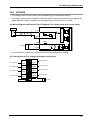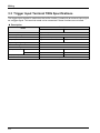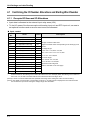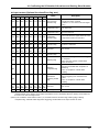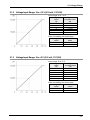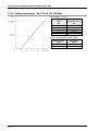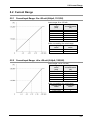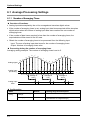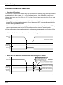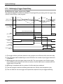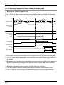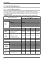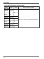
1
Safety Precautions Observe the following notices to ensure personal safety or to prevent accidents. To ensure that you use this product correctly, read this User’s Manual thoroughly before use. Make sure that you fully understand the product and information on safety. This manual uses two safety flags to indicate different levels of danger. WARNING If critical situations that could lead to user’s death or serious injury is assumed by mishandling of the product. -Always take precautions to ensure the overall safety of your system, so that the whole system remains safe in the event of failure of this product or other external factor. -Do not use this product in areas with inflammable gas. It could lead to an explosion. -Exposing this product to excessive heat or open flames could cause damage to the lithium battery or other electronic parts. CAUTION If critical situations that could lead to user’s injury or only property damage is assumed by mishandling of the product. -To prevent excessive exothermic heat or smoke generation, use this product at the values less than the maximum of the characteristics and performance that are assured in these specifications. -Do not dismantle or remodel the product. It could cause excessive exothermic heat or smoke generation. -Do not touch the terminal while turning on electricity. It could lead to an electric shock. -Use the external devices to function the emergency stop and interlock circuit. -Connect the wires or connectors securely. The loose connection could cause excessive exothermic heat or smoke generation. -Do not allow foreign matters such as liquid, flammable materials, metals to go into the inside of the product. It could cause excessive exothermic heat or smoke generation. -Do not undertake construction (such as connection and disconnection) while the power supply is on. It could lead to an electric shock. Copyright / Trademarks -This manual and its contents are copyrighted. -You may not copy this manual, in whole or part, without written consent of Panasonic Industrial Devices SUNX Co., Ltd. -Windows is a registered trademark of Microsoft Corporation in the United States and other countries. -All other company names and product names are trademarks or registered trademarks of their respective owners. PLC_ORG Introduction Thank you for buying a Panasonic product. Before you use the product, please carefully read the installation instructions and the users manual, and understand their contents in detail to use the product properly. Types of Manual • There are different types of users manual for the FP7 series, as listed below. Please refer to a relevant manual for the unit and purpose of your use. • The manuals can be downloaded on our website: http://industrial.panasonic.com/ac/e/dl_center/manual/ . Unit name or purpose of use Manual name Manual code FP7 CPU Unit Users Manual (Hardware) WUME-FP7CPUH FP7 CPU Unit Command Reference Manual WUME-FP7CPUPGR FP7 CPU Unit Users Manual (Logging Trace Function) WUME-FP7CPULOG FP7 CPU Unit Users Manual (Security Function) WUME-FP7CPUSEC FP7 CPU Unit Users Manual (LAN Port Communication) WUME-FP7LAN FP7 series Users Manual (SCU communication) WUME-FP7COM FP7 Extension Cassette (Communication) (Ethernet type) FP7 series Users Manual (Communication cassette Ethernet type) WUME-FP7CCET FP7 Extension (Function) Cassette Analog Cassette FP7 Analog Cassette Users Manual WUME-FP7FCA FP7 Digital Input/Output Unit FP7 Digital Input/Output Unit Users Manual WUME-FP7DIO FP7 Analog Input Unit FP7 Analog Input Unit Users Manual WUME-FP7AIH FP7 Analog Output Unit FP7 Analog Output Unit Users Manual WUME-FP7AOH FP7 Thermocouple Multianalog Input Unit FP7 Thermocouple Multi-analog Input Unit FP7 RTD Input Unit Users Manual WUME-FP7TCRTD FP7 Power Supply Unit FP7 CPU Unit Instructions for Built-in LAN Port Instructions for Built-in COM Port FP7 Extension Cassette (Communication) (RS-232C/RS485 type) FP7 RTD Input Unit FP7 High-speed counter Unit FP7 High-speed counter Unit Users Manual WUME-FP7HSC FP7 Pulse Output Unit FP7 Pulse Output Unit Users Manual WUME-FP7PG FP7 Positioning Unit FP7 Positioning Unit Users Manual WUME-FP7POSP FP7 Serial Communication Unit FP7 series Users Manual (SCU communication) WUME-FP7COM PHLS System PHLS System Users Manual WUME-PHLS Programming Software FPWIN GR7 FPWIN GR7 Introduction Guidance WUME-FPWINGR7 Table of Contents Table of Contents 1. Unit Functions and Restrictions ........................................ 1-1 1.1 Unit Functions and Operation................................................................. 1-2 1.1.1 Unit Type ................................................................................................. 1-2 1.1.2 Unit Type ................................................................................................. 1-3 1.2 Basic Operation of Analog Input Processing .......................................... 1-4 1.3 Restrictions on Units Combination ......................................................... 1-5 1.3.1 Restriction by Power Consumption ......................................................... 1-5 1.3.2 Applicable Versions of Unit and Software ............................................... 1-5 2. Names and Functions of Parts .......................................... 2-1 2.1 Analog Input Unit .................................................................................... 2-2 3. Wiring ................................................................................... 3-1 3.1 Wiring of Terminal Block ........................................................................ 3-2 3.2 Connecting Analog Input ........................................................................ 3-3 3.3 3.2.1 Precautions When Connecting Analog Input Signal ............................... 3-3 3.2.2 AFP7AD4H .............................................................................................. 3-3 3.2.3 AFP7AD8 ................................................................................................ 3-5 Trigger Input Terminal TRIG Specifications ........................................... 3-6 4. Unit Settings and data Reading ......................................... 4-1 4.1 ii Confirming the I/O Number Allocations and Starting Word Number............................ 4-2 Table of Contents 4.2 4.3 4.1.1 Occupied I/O Area and I/O Allocations ................................................... 4-2 4.1.2 Confirming the I/O Number Allocations ................................................... 4-5 Option settings ........................................................................................ 4-6 4.2.1 Configuration of Analog Input unit ........................................................... 4-6 4.2.2 Unit Setting and Conversion Processing Time ....................................... 4-9 Reading Analog Input Data................................................................... 4-10 4.3.1 4.4 Reading Analog Input Data ................................................................... 4-10 Data Acquisition Timing ........................................................................ 4-11 5. Conversion Characteristics of Analog Input Unit ............ 5-1 5.1 5.2 Voltage Range ........................................................................................ 5-2 5.1.1 Voltage Input Range: -10 to +10 V (0.32 mV, 1/62,500)......................... 5-2 5.1.2 Voltage Input Range: 0 to +10 V (0.32 mV, 1/31,250) ............................ 5-3 5.1.3 Voltage Input Range: 0 to +5 V (0.16 mV, 1/31,250) .............................. 5-3 5.1.4 Voltage input range: 1 to 5 V (0.16 mV, 1/25,000).................................. 5-4 Current Range ........................................................................................ 5-5 5.2.1 Current Input Range: 0 to +20 mA (0.64μA, 1/31,250) ........................... 5-5 5.2.2 Current Input Range: +4 to +20 mA (0.64μA, 1/25,000) ......................... 5-5 6. Optional Settings ................................................................. 6-1 6.1 Average Processing Settings.................................................................. 6-2 6.1.1 Number of Averaging Times ................................................................... 6-2 6.1.2 Time Average .......................................................................................... 6-3 6.1.3 Moving Average ...................................................................................... 6-4 6.2 Offset/Gain processing ........................................................................... 6-5 6.3 Scale Conversion.................................................................................... 6-7 6.4 Comparison for Upper and Lower Limits ................................................ 6-8 6.5 Holding Max./Min. Values ..................................................................... 6-11 iii Table of Contents 6.6 Disconnection detection ....................................................................... 6-14 6.7 Buffer Settings ...................................................................................... 6-16 6.8 6.7.1 Overview of Buffer Function .................................................................. 6-16 6.7.2 Buffering by Trigger Output Relay......................................................... 6-18 6.7.3 Buffering by External Input Trigger ....................................................... 6-20 6.7.4 Buffering Triggered by Value Change in Analog Input.......................... 6-22 Configuration by Programming ............................................................. 6-24 7. What to Do If an Error Occurs............................................ 7-1 7.1 What to Do If an Error Occurs (Analog Input) ........................................ 7-2 7.1.1 Failure in Reading Analog Input Data ..................................................... 7-2 7.1.2 Unstable Analog Input Conversion Value ............................................... 7-2 7.1.3 No Proper Conversion Values Obtained with Current Input ................... 7-2 8. Specifications ...................................................................... 8-1 8.1 Specifications ......................................................................................... 8-2 8.1.1 General Specifications ............................................................................ 8-2 8.1.2 Performance Specifications (AFP7AD4H) .............................................. 8-3 8.1.3 Performance Specifications (AFP7AD8) ................................................. 8-4 8.2 I/O Allocation .......................................................................................... 8-5 8.3 List of Unit Memories.............................................................................. 8-8 8.3.1 iv List of Unit Memory Number.................................................................... 8-8 8.4 List of Detailed Specifications of Unit Memories .................................. 8-10 8.5 Dimensions........................................................................................... 8-17 1 Unit Functions and Restrictions Unit Functions and Restrictions 1.1 Unit Functions and Operation 1.1.1 Unit Type Features of analog input unit The analog input unit receives various analog values (i.e., voltage, current, and temperature values) from laser analog sensors and pressure sensors and converts them internally into digital values. • The analog input unit can receive input through a number of channels. Analog input units: 4 channels (AD4H) / 8 channels (AD8) Six types of input ranges can be selected to support a variety of connecting equipment. • The speed of conversion, such as voltage/current range conversion, is as high as 25 μs/channel (non-isolated). • Converts input analog values into digital data with up to 16 bits in a resolution range of 1/25,000 to 1/62,500. 1-2 1.1 Unit Functions and Operation Various optional functions Functions to process loaded analog input data are provided. User programs can be simplified. Function Description Average processing settings Averages analog values obtained by sampling and stores them in the I/O area as digital values. It can be selected from No. of averaging times, time average and moving average. Offset/Gain processing settings Performs the correction of offset values (addition correct) or gain values (magnification correction), and stores the data after processing in the I/O area. Scale conversion setting This function is to scale-convert values to an easy-to-use data range. Converts values to digital values in the specified range (min. value and max. value), and stores the processed data in the I/O area. This function is convenient if used for unit conversion. Upper/lower limit value comparison setting This function compares acquired data with the upper limit and lower limit and turns ON the upper limit relay or lower limit relay if the acquired data exceeds the upper limit value or lower limit value. Max./Min. hold setting This function maintains the maximum and minimum values of acquired data. Holds the maximum and minimum digital conversion values when the maximum/minimum value hold setting is enabled, and stores the values in provided unit memories for each channel. Disconnection detection Turns ON the disconnection detection flag when input is disconnected or unconnected when selecting the range of 1-5 V 4-20 mA, and warns of the error state. Buffer function This function is to store digital conversion values loaded with a desired period. Any of the changes in user program, external digital input or analog input value can be selected as a trigger. 1.1.2 Unit Type Name Specifications Input 4ch Voltage input range: -10 to +10 V, 0 to +5 V, 1 to +5 V, -100 to +100 mV Input 8ch Current input range: 0 to +20 mA, 4 to +20 mA FP7 Analog I/O Unit Product no. AFP7AD4H AFP7AD8 1-3 Unit Functions and Restrictions 1.2 Basic Operation of Analog Input Processing Analog input is processed as explained below. Operation of analog input unit (1) Receiving analog input The analog input unit receives analog input data from analog devices, such as laser analog sensors and pressure sensors. (2) Digital conversion processing Analog input data received by the unit is converted into digital values in sequence automatically. (3) Storage of digital values A user program is used to read converted digital values as data in the input relay area (WX). Option setting The following option setting functions are provided for analog input processing. Any of the option setting functions can be set by writing the function to the unit memory (UM) by using the configuration menu of the FPWIN GR7 or a user program. • Average processing (number of times, time average, and moving average) • Scale conversion • Offset/Gain processing • Holding Max./Min. • Comparison for upper and lower limits • Disconnection detection • Buffering 1-4 1.3 Restrictions on Units Combination 1.3 Restrictions on Units Combination 1.3.1 Restriction by Power Consumption The unit has the following internal current consumption. Make sure that the total current consumption is within the capacity of the power supply with consideration of all other units used in combination with the analog input unit. Name Product no. Current consumption FP7 analog input unit (High-speed and High-accuracy type) AFP7AD4H 100 mA or less FP7 Analog Input Unit (Generalpurpose type) AFP7AD8 85 mA or less 1.3.2 Applicable Versions of Unit and Software For using the above units, the following versions of CPU units and software are required. Name Product no. FP7 Analog Input Unit (High-speed and Highaccuracy type) FP7 Analog Input Unit (General-purpose type) Applicable version CPU unit FPWINGR7 AFP7AD4H Ver.1.0 or later Ver.1.0 or later AFP7AD8 Ver.3.1 or later Ver.2.4 or later 1-5 Unit Functions and Restrictions 1-6 2 Names and Functions of Parts Names and Functions of Parts 2.1 Analog Input Unit Names and functions of parts (1) Operation monitor LEDs LED name LED color Contents - Blue Lit when the CPU unit is turned ON. ERROR Red Lit if the configuration settings are beyond the allowable range or A/D conversion is not possible. ALARM Red Lit if the hardware has an error. (2) Terminal block release lever To remove the analog input terminal block, push the release lever downward. (3) DIN rail attachment lever This lever is used to fix the unit to the DIN rail. (4) Unit Connector Connects to other I/O units and high-function units. (5) Analog input terminal block The terminal block is removable. Remove the terminal block before wiring. Solderless terminals for M3 can be used. (8) Fixing hook Used to secure the unit with another unit. 2-2 3 Wiring Wiring 3.1 Wiring of Terminal Block Suitable solderless terminals/wires M3 terminal screws are used for the terminal. The following suitable solderless terminals are recommended for the wiring to the terminals • Suitable solderless terminals Manufacturer Shape Part no. Suitable wires 1.25-MS3 1.25-B3A 2-MS3 2-N3A 0.25 to 1.65 mm 2 J.S.T. Mfg Co., Ltd. Round type Fork type Round type Fork type 1.04 to 2.63 mm 2 • Suitable wires Suitable wires 2 Tightening torque 2 AWG22 to 14 (0.3 mm to 2.0 mm ) 0.5 to 0.6N ∙m Connection to the terminal block Remove the terminal block before beginning the wiring operations. To remove the terminal block, push the release lever located at the top of the terminal block downward. Lock button <Bottom of unit> Install the terminal block by inserting it all the way to its original position and pressing the lock button on the bottom of the unit. Then confirm that the terminal block is securely attached and cannot be removed. 3-2 3.2 Connecting Analog Input 3.2 Connecting Analog Input 3.2.1 Precautions When Connecting Analog Input Signal • Use double-core twisted-pair shielded wires. It is recommended to ground them. However, depending on the conditions of the external noise, it may be better not to ground the shielding. • Do not have the analog input wiring close to AC wires, power wires, or load line from a device other than PLC. Also, do not bundle it with them. 3.2.2 AFP7AD4H • For the current input, connect the V and I terminals. • The trigger input terminal is used for using the buffer function with external input signals as trigger signals. It does not need to be connected when this function is not used. Wiring Diagram and Internal Circuit Diagram (For voltage input) Vn + In COMn Shield 250Ω 1MΩ TRIGn 24V DC T-COMn Internal circuit - PhotoMOS relay A/D conversion circuit Input device 910Ω 5.1kΩ Terminal layout (For voltage input) V1 For voltage input CH1 I1 COM1 V3 For voltage input CH3 I3 COM3 TRIG1 24V DC TRIG3 T-COM13 V0 I0 For voltage input CH0 COM0 V2 I2 For voltage input CH2 COM2 TRIG0 TRIG2 24V DC T-COM02 3-3 Wiring Wiring Diagram and Internal Circuit Diagram (For current input) Vn - In COMn Shield PhotoMOS relay 250Ω 1MΩ TRIGn 24V DC T-COMn Internal circuit + A/D conversion circuit Input device 910Ω 5.1kΩ (Note) For the current input, connect the V and I terminals. Terminal layout (For current input) V1 For current input CH1 I1 COM1 V3 For current input CH3 I3 COM3 TRIG1 24V DC TRIG3 T-COM13 V0 I0 For current input CH0 COM0 V2 I2 For current input CH2 COM2 TRIG0 TRIG2 24V DC T-COM02 (Note 1)TRIG0 to TRIG3 of AFP7AD4H indicate input terminal numbers. Note that they do not correspond to the analog inputs "CH0 to CH3". 3-4 3.2 Connecting Analog Input 3.2.3 AFP7AD8 • The voltage input and the current input switched by the configuration setting. • The trigger input terminal is used for using the buffer function with external input signals as trigger signals. It does not need to be connected when this function is not used. Wiring Diagram and Internal Circuit Diagram (For voltage input and current input) Vn / In + (*) - COMn TRIG 250Ω 2kΩ 24V DC Internal circuit Shield A/D conversion circuit Input device 680Ω T-COM (*) The connection of the circuit varies according to the configuration setting. Terminal layout (For voltage input and current input) For input CH1 For input CH3 For input CH5 For input CH7 V1 / I1 COM1 V3 / I3 COM3 V5 / I5 COM5 V7 / I7 COM7 T-COM V0 / I0 COM0 V2 / I2 COM2 V4 / I4 COM4 V6 / I6 COM6 TRIG For input CH0 For input CH2 For input CH4 For input CH6 24V DC 3-5 Wiring 3.3 Trigger Input Terminal TRIG Specifications The trigger input terminal is used when the buffer function is used with an external input signal as a trigger signal. This terminal needs not be connected if these functions are not used. Description Description Items AFP7AD4H AFP7AD8 Insulation system Optical coupler Rated input voltage 24 V DC Rated input current Approx. 4.5 mA (at 24 V) Approx. 12 mA (at 24 V) Input impedance Approx. 5.1kΩ Approx. 2kΩ Operating voltage range 21.6 to 26.4 V DC Min. ON voltage/Min. ON current 19.2 V/3.5 mA Max. OFF voltage/Max. OFF current 5 V/1.5 mA Response time OFF→ON 0.2 ms or less ON→OFF 0.1 ms or less 0.2 ms or less 0.1 ms or less Input points per common 2 point/1 common 1 point/1 common External connection method Terminal block connections (M3 terminal screws) 3-6 4 Unit Settings and data Reading Unit Settings and data Reading 4.1 Confirming the I/O Number Allocations and Starting Word Number 4.1.1 Occupied I/O Area and I/O Allocations • Input data is allocated to the external input relay areas (WX). • To the I/O areas of the thermocouple multi analog input unit and RTD input unit, an area to set optional functions and an area to reset errors are allocated. Input contact I/O area No. Name Default Description WX0 CH0 Analog conversion data K0 WX1 CH0 Optional function flag H0 WX2 CH1 Analog conversion data K0 WX3 CH1 Optional function flag H0 WX4 CH2 Analog conversion data K0 Digital converted values corresponding to the analog input is stored. WX5 CH2 Optional function flag H0 <Voltage range> WX6 CH3 Analog conversion data K0 -10 to +10 V: -31,250 to +31,250 0 to +10 V or 0 to +5 V: 0 to +31,250 Analgo conversion data area WX7 CH3 Optional function flag H0 WX8 CH4 Analog conversion data K0 +1 to +5 V: 0 to +25,000 <Current range> WX9 CH4 Optional function flag H0 WX10 CH5 Analog conversion data K0 WX11 CH5 Optional function flag H0 WX12 CH6 Analog conversion data K0 WX13 CH6 Optional function flag H0 WX14 CH7 Analog conversion data K0 WX15 CH7 Optional function flag H0 0 to +20 mA: 0 to +31,250 +4 to +20 mA: 0 to +25,000 Optional function flag area Refer to the table on the next page. (Note 1): The I/O numbers in the table indicates offset addresses. The I/O numbers actually allocated are the numbers based on the starting word number allocated to the unit. Example) When the starting word number for the unit is "10", the A/D conversion data of CH0 is WX10 and the error flag is X11F. (Note 2) It is A/D conversion data within the specified scale range when setting the scale conversion setting. (Note 3) The digital converted value corresponding to about 2 V of analog input is displayed for channels which are not connected to input when setting the voltage range with AFP7AD8. 4-2 4.1 Confirming the I/O Number Allocations and Starting Word Number Input contact (Optional functions/Error flag area) I/O No. CH0 CH1 CH2 CH3 CH4 CH5 CH6 CH7 Name Description X10 X30 X50 X70 X90 X110 X130 X150 Disconnection detection flag ON with disconnection detected and OFF with disconnection restored. (Valid for 1 to 5 V and 4 to 20 mA ranges only) X11 X31 X51 X71 X91 X111 X131 X151 Upper limit comparison relay Turns ON when the value exceeds the set upper limit. X12 X32 X52 X72 X92 X112 X132 X152 Lower limit comparison relay Turns OFF when the value drops below the set lower limit. X13 X33 X53 X73 Upper/Lower limit X93 X113 X133 X153 comparison execution flag Turns ON when the upper limit/lower limit comparison function is executed. X14 X34 X54 X74 X94 X114 X134 X154 Not used Do not use. Turns ON when the max./min. hold function is executed. Do not use. X15 X35 X55 X75 Max./Min. hold X95 X115 X135 X155 execution flag X16 to X17 X36 to X37 X56 to X57 X76 to X77 X96 X116 X136 X156 to to to Not used to X97 X117 X137 X157 X18 - - - - - - - Buffer function execution flag On when the buffer function is executed. X19 - - - - - - - Buffering flag ON when buffering starts after the trigger is accepted. OFF when the number of buffer data items is reached. X1A X1B - - - - - - - - - - - - - - Buffering completion flag Data before triggering enable flag ON when the shared memory has become accessible after completion of buffering. OFF on completion of buffer data reading. ON when the number of buffer data items before triggering has reached the set value. OFF on completion of buffer data reading. X1C to X1E X3C X5C X7C X9C X11C X13C X15C to to to to to to to Not used X3E X5E X7E X9E X11E X13E X15E Do not use. X1F X3F X5F X7F X9F X11F X13F X15F Error flag Turns ON when an error occurs (Note 1): The I/O numbers in the table indicates offset addresses. The I/O numbers actually allocated are the numbers based on the starting word number allocated to the unit. Example) When the starting word number for the unit is "10", the error flag is X11F. (Note 2) The conditions of the buffer function (i.e., the buffer function execution flag, buffering flag, buffering completion flag, and data enable flag before triggering) are allocated to the input contacts for CH0. 4-3 Unit Settings and data Reading Output contact (Optional functions/Error flag area) I/O No. CH0 CH1 CH2 CH3 CH4 CH5 CH6 CH7 Name Description Y0 Y10 Y20 Y30 Y40 Y50 Y60 Y70 Disconnection detection execution relay ON to execute the disconnection detection function. OFF to turn OFF the disconnection detection flag (Xn0). (Valid for 1 to 5 V and 4 to 20 mA ranges only) Y1 Y2 Y11 Y12 Y21 Y22 Y31 Y32 Y41 Y42 Y51 Y52 Y61 Y62 Y71 Y72 Not used Do not use. ON to execute the function to compare the upper and lower limits. OFF to turn OFF the upper limit comparison relay (Xn1) and lower limit comparison relay (Xn2). Y3 Y13 Y23 Y33 Y43 Y53 Y63 Y73 Upper/Lower limit comparison execution relay Y4 Y14 Y24 Y34 Y44 Y54 Y64 Y74 Not used Do not use. ON to execute the max./min. hold function. Do not use. Y5 Y15 Y25 Y35 Y45 Y55 Y65 Y75 Max./Min. hold execution relay Y6 Y16 Y26 Y36 Y46 Y56 Y66 Y76 Not used Y7 Y17 Y27 Y37 Y47 Y57 Y67 Y77 Not used Do not use. Y8 - - - - - - - Buffer execution relay When the buffer function is enabled, trigger acceptance will be permitted with the buffer execution relay turned ON.The internal state transition will be initialized with the buffer execution relay turned OFF. Y9 - - - - - - - Buffer trigger relay If "Trigger relay" is set in trigger setting, triggering will start with the trigger relay turned ON. Buffer data read completion relay ON for one scan upon completion of readign buffer data from the shared memory with a user program. Goes to the state of trigger acceptance permitted after clearing the buffer memory. YA - - - YB to YE Y1B to Y1E Y2B Y3B Y4B to to to Y2E Y3E Y4E Y5B Y6B Y7B to to to Y5E Y6E Y7E Not used Do not use. YF Y1F Y2F Y5F Error flag reset relay Resets an error flag. Y3F - Y4F - - Y6F - Y7F (Note 1): The I/O numbers in the table indicates offset addresses. The I/O numbers actually allocated are the numbers based on the starting word number allocated to the unit. Example) When the starting word number for the unit is "10", the disconnection detection execution relay of CH0 is Y100, and the error flag reset relay is Y10F. (Note 2) The operation of the buvver function (consisting of the buffer execution relay, buffer trigger relay, and buffer data read completion relay) is specified by the output contacts for CH0. 4-4 4.1 Confirming the I/O Number Allocations and Starting Word Number 4.1.2 Confirming the I/O Number Allocations • I/O numbers and base word numbers are always necessary when writing programs. Always check to see if the numbers match the design. • I/O numbers allocated to the analog input unit are determined by the first word number. Allocations to unit Take the following procedure to set the first word number. PROCEDURE 1. Select "Options" > "FP7 Configuration" > "I/O map" in the menu bar. The "I/O map" dialog box is displayed. 2. Double-click the target slot where the operating unit is to be inserted. 3. Select “Analog I/O” and “Input Unit” in the unit selection field. The following dialog box shows the case of AFP7AD4H. 4. Press the [OK] button. The first word number specified is set. 4-5 Unit Settings and data Reading 4.2 Option settings 4.2.1 Configuration of Analog Input unit Use the FPWIN GR7 configuration menu to make analog input unit settings, such as input range and isolation/non-isolation settings. Setting method The following steps are described on the condition that the analog input unit has been already allocated on the I/O map. PROCEDURE 1. Select “Options” > “FP7 Configuration” > “I/O map” from the menu bar. The "I/O map" dialog box is displayed. 2. Select the slot where the analog input unit is registered and press the [Advanced] button. The “Analog unit settings” dialog box is displayed. 3. Select a setting to be set from the left pain, and set desired items. The following explanation shows the case of CH0 setting. Displayed items vary depending on the unit types and selected items. 4. Press the [OK] button. The set value will become effective when the set value is downloaded together with a corresponding program as a project. 4-6 4.2 Option settings Settings (AFP7AD4H) Group Basic setting items (common to all channels) Basic setting items (per channel) Option setting items (per channel) Setting item Settings Default Isolation between channels Non-isolated/Isolated Non-isolated Buffer function Not use/Use Not use Trigger type Trigger input relay/rise of external input trigger/fall of external input trigger/rising time of analog input level/falling time of analog input level Trigger input relay External input trigger Unused/TRIG0/TRIG1/TRIG2/TRIG3 Not used Input level trigger CH Unused/CH0/CH1/CH2/CH3 Not used No. of buffer data items 1 to 10,000 1000 No. of data items before triggering 0 to 9,999 0 Trigger cycle 1 to 30,000 1 Analog input trigger level -31,250 to +31,250 0 Conversion processing Execute/Not execute Execute Range setting -10 to +10 V 0 to +10 V 0 to +5 V +1 to +5 V 0 to +20 mA +4 to +20 mA -10 to +10 V Average processing settings Not execute/No. of averaging times/time average/moving average Not execute Offset/Gain processing Not execute/Execute Not execute Scale conversion Not execute/Execute Not execute Comparison settings for upper and lower limits Not execute/Execute Not execute Max./Min. hold Not execute/Execute Not execute Disconnection detection settings Not execute/Execute Not execute Disconnection detection reset Auto/Manual Auto Averaging constant Times: 2 to 60,000 [times] Time (non-isolated): 1 to 1,500 [ms] Time (isolated): 200 to 60,000 [ms] Moviing average: 2 to 2,000 [times] 200 Offset value -3,000 to +3,000 0 Gain value +9,000 to +11,000 +10,000 Scale conversion max. value -30,000 to +30,000 10,000 Scale conversion min. value -30,000 to +30,000 0 Upper limit comparison ON level -31,250 to +31,250 0 Upper limit comparison OFF level -31,250 to +31,250 0 Lower limit comparison ON level -31,250 to +31,250 0 Lower limit comparison OFF level -31,250 to +31,250 0 4-7 Unit Settings and data Reading Settings (AFP7AD8) Group Setting item Isolation between channels Basic setting items (common to all channels) Basic setting items (per channel) Option setting items (per channel) 4-8 Settings Default Non-isolated only Non-isolated Buffer function Not use/Use Not use Trigger type Trigger input relay/rise of external input trigger/fall of external input trigger/rising time of analog input level/falling time of analog input level Trigger input relay Input level trigger CH Unused/CH0/CH1/CH2/CH3/HC4/ CH5/CH6/CH7 Not used No. of buffer data items 1 to 8,000 1000 No. of data items before triggering 0 to 7,999 0 Trigger cycle 1 to 30,000 1 Analog input trigger level -31,250 to +31,250 0 Conversion processing Execute/Not execute Execute Range setting -10 to +10 V 0 to +10 V 0 to +5 V +1 to +5 V 0 to +20 mA +4 to +20 mA -10 to +10 V Average processing settings Not execute/No. of averaging times/time average/moving average Not execute Offset/Gain processing Not execute/Execute Not execute Scale conversion Not execute/Execute Not execute Comparison settings for upper and lower limits Not execute/Execute Not execute Max./Min. hold Not execute/Execute Not execute Disconnection detection settings Not execute/Execute Not execute Disconnection detection reset Auto/Manual Auto Averaging constant Times: 2 to 60,000 [times] Time (non-isolated): 1 to 1,500 [ms] Time (isolated): 200 to 60,000 [ms] Moviing average: 2 to 2,000 [times] 200 Offset value -3,000 to +3,000 0 Gain value +9,000 to +11,000 +10,000 Scale conversion max. value -30,000 to +30,000 10,000 Scale conversion min. value -30,000 to +30,000 0 Upper limit comparison ON level -31,250 to +31,250 0 Upper limit comparison OFF level -31,250 to +31,250 0 Lower limit comparison ON level -31,250 to +31,250 0 Lower limit comparison OFF level -31,250 to +31,250 0 4.2 Option settings 4.2.2 Unit Setting and Conversion Processing Time Conversion time varies with the configuration setting conditions. Isolation setting and conversion processing time • Isolated: 5 ms/ch • Non-isolated: 25 μs/ch • The speed of A/D conversion processing will become faster if non-isolation is set. Each channel is isolated by switching the respective photo-MOS relays of the channels at the time of conversion. The photo-MOS relays are always turned ON at the time of non-isolation and the commons will be shared. • For AFP7AD8, only the non-isolated setting is available. Conversion processing execution/non-execution setting and conversion processing time Select the execution or non-execution of the conversion processing of analog input on a channel-by-channel basis. This can save the conversion time for channels that do not execute conversion processing. Example) Conversion time for four channels Converted in the order of ch0→ch1→ch2→ch3→ch0→ch1→ch2→ch3→.... (1 cycle = 100 μs at the time of non-isolation) Example) Conversion time for two channels (with CH2 and CH3 excluded). Conversion is executed in the order of ch0→ch1→ch0→ch1→ch0→ch1→ch0→ch1→... and the conversion time for CH2 and CH3, which are excluded, is saved. (1 cycle = 50 μs at the time of non-isolation) 4-9 Unit Settings and data Reading 4.3 Reading Analog Input Data 4.3.1 Reading Analog Input Data Basic Operation of Analog Input Processing (1) Receiving analog input The analog input unit receives analog input data from devices, such as laser analog sensors and pressure sensors. (2) Digital conversion processing Analog input data received by the unit is converted into digital values in sequence automatically in the unit. The converted digital value varies with the setting of the range. (3) Storage of digital values A user program is used to read converted digital values as data in the input relay area (WX). The specified area number varies depending on the installation position of the unit. V or I t Program to Acquire Converted Digital Values Reading the values in digital conversion value storage areas WX10, WX12, WX14, and WX16 to any areas of data registers ranging from DT100 to DT103. R0 4-10 MV.SS WX10 CH0 input DT100 MV.SS WX12 CH1 input DT101 MV.SS WX14 CH2 input DT102 MV.SS WX16 CH3 input DT103 Transferring the digital data in analog input areas WX10, WX12, WX14, and WX16 to data registers ranging from DT100 to DT103. 4.4 Data Acquisition Timing 4.4 Data Acquisition Timing Input conversion processing time of analog input unit Conversion processing time varies with the range and the number of channels in use. The conversion execution/non-execution channel function can save the conversion time for channels that do not execute conversion processing. Example of 2-channel conversion Converted in the order of ch0→ch1→ch0→ch1→.... Data acquisition timing of CPU unit • Digital values converted by the analog input unit are input into the CPU unit at the I/O refreshing timing of the CPU unit. • The conversion processing of the analog input unit is not synchronized with the I/O refreshing timing of the CPU unit. Therefore, the latest data is input into the operation memory of the CPU unit when the CPU unit implements I/O refreshing. • Example of 4-channel conversion b c a d Analog signal of ch0 Processing in the analog input part e Converts in the order of ch0→ch1→ch2→ch3 0 1 2 3 0 1 2 3 0 1 2 3 0 1 2 3 0 I/O refresh Processing in the CPU unit Data of ch0 to be read in the CPU unit a b c d 4-11 Unit Settings and data Reading • Example of 1-channel conversion Analog signal of ch0 a c b e d f g h i j k l m n o p q r Converts ch0 repeatedly Processing in the analog input part I/O refresh Processing in the CPU unit Data of ch0 to be read in the CPU unit 4-12 a c e g j l n p 5 Conversion Characteristics of Analog Input Unit Conversion Characteristics of Analog Input Unit 5.1 Voltage Range 5.1.1 Voltage Input Range: -10 to +10 V (0.32 mV, 1/62,500) Input range: -10 to +10 V Analog input value (V) Digital conveted value (K) +10 +8 +6 +4 +2 0 -2 -4 -6 -8 -10 +31,250 +25,000 +18,750 +12,500 +6,250 0 -6,250 -12,500 -18,750 -25,000 -31,250 When exceeding the rated range 5-2 Analog input value Converted value +10 V or more -10V or less +31,250 -31,250 5.1 Voltage Range 5.1.2 Voltage Input Range: 0 to +10 V (0.32 mV, 1/31,250) Input range: 0 to +10 V Analog input value (V) Digital conveted value (K) +10 +8 +6 +4 +2 0 +31,250 +25,000 +18,750 +12,500 +6,250 0 When exceeding the rated range Analog input value Converted value +10 V or more 0 V or less +31,250 0 5.1.3 Voltage Input Range: 0 to +5 V (0.16 mV, 1/31,250) Input range: 0 to +5 V Analog input value (V) Digital conveted value (K) +5 +4 +3 +2 +1 0 +31,250 +25,000 +18,750 +12,500 +6,250 0 When exceeding the rated range Analog input value Converted value +5 V or more 0 V or less +31,250 0 5-3 Conversion Characteristics of Analog Input Unit 5.1.4 Voltage input range: 1 to 5 V (0.16 mV, 1/25,000) Input range: 1 to 5 V Analog input value (V) Digital conveted value (K) 5 4 3 2 1 25,000 18,750 12,500 6,250 0 When exceeding the rated range 5-4 Analog input value Converted value 5 V or more 1 V or less 25,000 0 5.2 Current Range 5.2 Current Range 5.2.1 Current Input Range: 0 to +20 mA (0.64μA, 1/31,250) Input range: 0 to +20 mA Analog input value (mA) Digital conveted value (K) +20 +16 +12 +8 +4 0 +31,250 +25,000 +18,750 +12,500 +6,250 0 When exceeding the rated range Analog input value Converted value +20 mA or more 0 mA or less +31,250 0 5.2.2 Current Input Range: +4 to +20 mA (0.64μA, 1/25,000) Input range: +4 to +20 mA Analog input value (mA) Digital conveted value (K) +20 +16 +12 +8 +4 +25,000 +18,750 +12,500 +6,250 0 When exceeding the rated range Analog input value Converted value +20 mA or more +4 mA or less +25,000 0 5-5 Conversion Characteristics of Analog Input Unit 5-6 6 Optional Settings Optional Settings 6.1 Average Processing Settings 6.1.1 Number of Averaging Times Overview of functions • Analog input data sampled by the unit is averaged and stored as digital values. • If the number of averaging times is set, analog input data items acquired will be stored as digital values when the number of analog input data items reaches the set number of averaging times. • If the number of data items acquired is less than the number of averaging times, the acquired data will be stored in the I/O area. • Obtain the number of averaging times to be processed from the following input. Input: The sum of analog input data items for the number of averaging times Output: Number of averaging times value Processing during the number of averaging times Averaging setting example: The number of averaging times is set to 5. a b c e d f g h Analog signal i j k l m n o p q r Analog input processing Average of a to e Average of f to j Average of k to o Analog input data Configuration Name Function setting 6-2 Default Setting range and description Average processing settings Not execute Select “the number of averaging times.” Averaging constant K200 Number: 2 to 60,000 [times] (specified with an unsigned integer) 6.1 Average Processing Settings 6.1.2 Time Average Overview of functions • Analog input data sampled by the unit is averaged and stored as digital values. • If time average is set, analog input data items acquired will be stored as digital values when the acquisition period of the analog input data items reaches the set averaging time. • Obtain the time average to be processed from the following input. Input: The sum of analog input data items for the number of averaging time Output: Time average value Processing during time average Average setting example: Example of an averaging time of 5 ms Elapse of 5 ms A0 A1 An A2 Elapse of 5 ms C0 B0 Analog signal Analog input processing B1 C1 Bn C2 B2 ・・・・・ ・・・・・ ・・・・・ ・・・・・ ・・・・・ ・・・・・ Average of A0 to An Average of B0 to Bn Analog input data Configuration Name Function setting Default Setting range and description Average processing settings Not execute Select “time average.” Averaging constant K200 Time (non-isolated): 1 to 1,500 [ms] Time (isolated): 200 to 60,000 [ms] (For AD4H only) (Specified with an unsigned integer) 6-3 Optional Settings 6.1.3 Moving Average Overview of functions • Analog input data sampled by the unit is averaged and stored as digital values. • If moving average is set, analog input data items acquired will be stored as digital values when the number of analog input data items reaches the set number of moving average times. • Obtain the number of averaging times to be processed from the following input. Input: The number of average times, analog input data for the number of average times, the latest analog input data, and old analog input data Output: Moving average value Processing during moving average Averaging setting example: The number of averaging times is set to 15. a b c d e f g h i j Analog signal k l m n o p q r ・・・ Average of a to o Average of b to p Analog input processing Average of c to q Analog input data ・・・ ・・・ Configuration Name Function setting 6-4 Default Setting range and description Average processing settings Not execute Select “moving average.” Averaging constant K200 2 to 2,000 [times] (specified with an unsigned integer) 6.2 Offset/Gain processing 6.2 Offset/Gain processing Overview of Functions • Offset value (added correction) and gain value (magnification correction) adjustments are made to store processed data in the I/O area. Analog input data Offset processing Gain processing Analog postprocessing data • Offset value settings are used as a function (zero-point adjustment) to make offset error adjustments between load devices. If the analog conversion value is K50 when the analog input value is 0 V, the analog conversion data is corrected to 0 V based on K-50 as an offset value. (K) (K) 50 (V) (V) Offset processing • Gain value settings are used as a function to adjust delicate scale errors between load devices. The gain value slope can be changed in a range of x0.9 to x1.1. (K) (K) (V) Gain processing Gain x 1.1 Gain x 0.9 (V) • Offset/Gain processing is executed on a channel-by-channel basis. 6-5 Optional Settings Configuration Name Default Setting range and description Not execute Select “Execute.” Offset value K0 Set an offset value at the time of using the offset processing function. Gain value K10,000 Function setting Offset/Gain processing Setting range: -3,000 to +3,000 (specified with a signed integer) Set an gain value at the time of using the gain processing function. Setting range: +9,000 to 1+1,000 (0.9x to 1.1x: Specified with a signed integer) The offset value is corrected to a value corresponding to the resolution of the input range of the original value regardless of whether scale conversion is set or not. 6-6 6.3 Scale Conversion 6.3 Scale Conversion Overview of functions • This function is to scale-convert values to an easy-to-use data range. It converts values to digital values in the specified range (min. value and max. value), and stores the processed data in the I/O area. This function is convenient if used for unit conversion. • Scale conversion is executed on a channel-by-channel basis. • Conversion values read from the analog input unit include fractions. Therefore, convert the values to easy-to-handle figures if needed. (K) (K) 25000 10000 12500 Scale conversion 1 3 5 (V) 5000 1 3 5 (V) Configuration Name Default Setting range and description Not execute Select “Execute.” Minimum value of scale conversion K0 Set the minimum value at the time of using the scale conversion function. Maximum value of scale conversion K10,000 Function setting Scale conversion Setting range: -30,000 to +30,000 (specified with a signed integer) Set the maximum value at the time of using the scale conversion function. Setting range: -30,000 to +30,000 (specified with a signed integer) * If data outside the minimum or maximum scale is input, scale conversion will be disabled and the minimum or maximum scale value will be stored as a conversion value. 6-7 Optional Settings 6.4 Comparison for Upper and Lower Limits Overview of Functions This function compares acquired data with the upper limit and lower limit and turns ON the upper limit relay or lower limit relay if the acquired data exceeds the upper limit value or lower limit value. • Comparison for upper and lower limits is executed on a channel-by-channel basis. • The upper limit relay will turn ON if the digital conversion value is larger than the upper limit. • The lower limit relay will turn ON if the digital conversion value is smaller than the lower limit. • The function will be disabled with the comparison execution relay (Y) turned ON if the configuration-upper/lower limit comparison setting is not executed. (K) Upper limit comparison ON level (2) Upper limit comparison OFF level (3) Digital converted value Lower limit comparison OFF level Lower limit comparison ON level (4) (Flag) Comparison execution relay (*1) Upper limit comparison relay (*1) (1) (5) Lower limit comparison relay (*3) Comparison execution flag (*4 ) (t) (1) The upper/lower limit comparison function will be executed when the user program turns ON the comparison execution relay. (2) The upper limit comparison relay will turn ON if the upper limit comparison ON level or an upper level is detected (3) The upper limit comparison relay will turn OFF if the upper limit comparison OFF level or a lower level is detected. (4) The lower limit comparison relay will turn ON if the lower limit comparison ON level or a lower level is detected. (5) The upper/lower limit comparison relay and comparison execution flag will be forcibly turned OFF if the comparison execution relay is turned OFF. 6-8 6.4 Comparison for Upper and Lower Limits I/O Allocation The I/O numbers in the timing chart and program are shown on the condition that the first word number of the unit is 10. Actual I/O numbers allocated to the analog input unit are determined by the first word number. CH0 CH1 CH2 CH3 CH4 CH5 CH6 *1 Comparison execution relay Y103 Y113 Y123 Y133 *2 Upper limit comparison relay X111 X131 X151 X171 CH7 Y143 Y153 Y163 Y173 X191 X211 X231 X251 *3 Lower limit comparison relay X112 X132 X152 X172 X192 X212 X232 X252 *4 Comparison execution flag X113 X133 X153 X173 X193 X213 X233 X253 Configuration Name Default Setting range and description Not execute Select the desired function to be used. Upper/Lower limit comparison Upper limit comparison ON level K0 Set the upper limit to turn ON the output flag at the time of using the upper/lower limit comparison function. Upper/Lower limit comparison Upper limit comparison OFF level K0 Upper/Lower limit comparison Lower limit comparison OFF level K0 Upper/Lower limit comparison Lower limit comparison ON level K0 Function setting Upper limit / Lower limit comparison Setting range: -31,250 to +31,250 (specified with a signed integer) Set the upper limit to turn OFF the output flag at the time of using the upper/lower limit comparison function. Setting range: -31,250 to +31,250 (specified with a signed integer) Set the lower limit to turn OFF the output flag at the time of using the upper/lower limit comparison function. Setting range: -31,250 to +31,250 (specified with a signed integer) Set the lower limit to turn ON the output flag at the time of using the upper/lower limit comparison function. Setting range: -31,250 to +31,250 (specified with a signed integer) (Note) Make the following level settings for upper/lower limit comparison. Lower limit comparison ON level ≤ Lower limit comparison OFF level < Upper limit comparison OFF level ≤ Upper limit comparison ON level 6-9 Optional Settings Sample Program The digital conversion value on ch0 of the analog input unit is read to detect the upper limit and lower limit, and the desired output is turned ON with the upper or lower limit detected. R0 ( DF ) R1 X113 ( DF ) X111 Comparison Upper limit execution comparison flag relay X113 X112 Comparison Lower limit comparison execution relay flag 6-10 Y103 < SET > (CH0): Upper/Lower limit comparison execution relay Y103 < RST > (CH0): Upper/Lower limit comparison execution relay Y200 Y201 (CH0): Controls upper and lower limit comparison function R0 ON: Comparison execution R1 ON: Turns OFF comparison execution relay. (CH0): Turns ON Y200 when the value exceeds the upper limit. (CH0): Turns ON Y201 when the value drops below the lower limit. 6.5 Holding Max./Min. Values 6.5 Holding Max./Min. Values Overview of Functions This function maintains the maximum and minimum values of acquired data. When the maximum and minimum value hold settings are valid, the maximum and minimum digital conversion values will be maintained and stored in the following unit memories. • If the function has not been enabled with the configuration settings, the function will not work with the hold execution relay turned ON. • When the hold execution relay is turned ON, the values at that time will be preset as maximum and minimum values in the unit memories. • The maximum and minimum values will be stored in the unit memories even if the hold execution relay is turned OFF or the unit is set into PROG. mode. • The maximum and minimum values are held on a channel-by-channel basis. (K) Holds min. value in unit memory Holds max. value in unit memory Digital conversion value (Flag) Hold execution relay (*1) Hold execution flag (*2) Unit memory Refreshes max. value Refreshes min. value Refreshes min. value (t) 6-11 Optional Settings Hold data storage area Unit memory number (Hex) Name Default Setting range and description Holding max. value K0 The acquired maximum value will be held when the maximum and minimum value holding function is used. UM 00180 UM 00181 UM 00182 UM 00183 UM 00184 Setting range: -31,250 to 31,250 (specified with a signed integer) UM 00185 UM 00186 UM 00187 UM 00188 UM 00189 UM 0018A UM 0018B UM 0018C Holding min. value The acquired minimum value will be held when the maximum and minimum value holding function is used. K0 Setting range: -31,250 to 31,250 (specified with a signed integer) UM 0018D UM 0018E UM 0018F (Note) The unit memory numbers in the above table are listed for CH0 to CH7 in numerical order. I/O allocation The I/O numbers in the timing chart and program are shown on the condition that the first word number of the unit is 10. Actual I/O numbers allocated to the analog input unit are determined by the first word number. CH0 CH1 CH2 CH3 CH4 CH5 CH6 CH7 *1 Hold execution relay Y105 Y115 Y125 Y135 Y145 Y155 Y165 Y175 *2 Hold execution flag X115 X135 X155 X175 X195 X215 X235 X255 Configuration Name Default Setting range and description Not execute Select “Execute.” Holding min. value K0 Holding min. value (-31,250 to +31,250) Holding max. value K0 Holding max. value (-31,250 to +31,250) Function setting 6-12 Holding max./min. values 6.5 Holding Max./Min. Values Sample Program The analog data on ch0 of the analog input unit is read, and the data holding the maximum and minimum values will be read at the desired data register. R0 Y105 < SET > Max./Min. value hold execution relay Y105 < RST > Max./Min. value hold execution relay ( DF ) R1 ( DF ) X115 (CH0): Controls upper and lower limit comparison function. ON: Execute OFF: Don't execute MV.SS S1: UM00180 Unit memory specified for slot 1 DT0 (CH0): Copies max. value to DT0 MV.SS S1: UM00188 Unit memory specified for slot 1 DT1 (CH0): Copies min. value to DT1 Max./Min. value hold execution flag 6-13 Optional Settings 6.6 Disconnection detection Overview of Functions This function is to announce an error with the disconnection detection flag if the input is below a certain value in either range, +1 to +5V of voltage input or +4 to +20 mA of current input. Voltage input range of +1 to +5 V set: 0.7 V or less; Current input range of +4 to +20 mA set: 2.8 mA max. • If the input exceeds the above value while the disconnection detection execution relay is turned ON, the disconnection detection flag will be turned OFF automatically, provided that the auto setting has been made. • If the manual reset setting is made, the disconnection detection flag will be turned OFF by using a user program and turning OFF the disconnection detection execution relay. • If the configuration-disconnection detection setting has not been made, the function will be disabled with the disconnection detection execution relay turned ON. Action with the detection disconnection reset setting set to auto (V) Analog input value Disconnection threshold 0.7 V or 2.8 mA (Flag) Disconnection detection execution relay (*1) Disconnection detection flag (*2) (t) Action with the detection disconnection reset setting set to manual (V) Analog input value (Flag) Disconnection detection execution relay (*1) Disconnection detection flag (*2) While in manual mode, the disconnection detection flag (X) will not automatically turn OFF when the voltage is recovered. Disconnection threshold 0.7 V or 2.8 mA The disconnection detection flag (X) is turned OFF with the disconnection detection execution relay turned OFF. (t) 6-14 6.6 Disconnection detection I/O allocation The I/O numbers in the timing chart and program are shown on the condition that the first word number of the unit is 10. Actual I/O numbers allocated to the analog input unit are determined by the first word number. CH0 CH1 CH2 CH3 CH4 CH5 CH6 CH7 *1 Disconnection detection execution relay Y100 Y110 Y120 Y130 Y140 Y150 Y160 Y170 *2 Disconnection detection flag X110 X130 X150 X170 X190 X210 X230 X250 Configuration Name Function setting Default Setting range and description Disconnection detection Not execute Select “Execute.” Disconnection detection reset Auto Select “Auto.” Sample Program R0 ( DF ) R1 ( DF ) X110 Y100 < SET > Disconnection detection execution relay Y100 < RST > Y200 Disconnection detection flag (CH0): Controls disconnection detection execution function. ON: Execute OFF: Turns OFF disconnection detection flag. (CH0): Turns Y200 ON at the time of disconnection detection. Not executed unless a voltage input range of +1 to +5 V or current input range of +4 to +20 mA is set. 6-15 Optional Settings 6.7 Buffer Settings 6.7.1 Overview of Buffer Function This function stores digital conversion values acquired at a preset cycle into a unit memory. If a trigger is input while the buffer function is executed (with the buffer execution relay turned ON), digital conversion values for a specified number of data items will be stored in the buffer memory (unit memory) at a specified cycle. Specify execution conditions (trigger settings, the number of buffer data items, and cycle) Buffer function configuration Buffer function ON Starts the buffering of pre-trigger digital conversion values at the specified cycle Starts execution Trigger ON Starts the buffering of digital conversion values at the specified cycle Buffering Buffering completion Reads buffer data from the CPU unit Buffer data read Executes buffering Digital conversion value Analog input processing Buffer (Unit memory) Buffer trigger ・・・・・ Completion of acquisition ・・・・・ Pre-trigger data buffering Post-trigger data buffering Aligns and stores the contents in the shared memory on completion of acquisition CH0 CH1 CH2 CH3 CH0 buffer areas UM 00800 to UM 02F0F (10,000 words) CH1 buffer areas UM 03000 to UM 0570F (10,000 words) CH2 buffer areas UM 05800 to UM 07F0F (10,000 words) CH3 buffer areas UM 08000 to UM 0A70F (10,000 words) • If the configuration-disconnection detection setting has not been set to “not execute”, the function will be disabled even if the buffer execution relay is turned ON. 6-16 6.7 Buffer Settings Configuration Name Default Setting range and description Execution/Nonexecution settings Not use Select "Use" for the buffer function. Trigger setting H0 Select a trigger signal to start buffering when the buffer function is used. Buffer function Set the number of data items (words) to be stored in the buffer. No. of buffer data items K1000 Setting range: +1 to +10,000 (AFP7AD4H), +1 to +8,000 (AFP7AD8) * The number of buffer data items is the total sum of data items including the number of data items before triggering Set the number of data items (words) before triggering. No. of data items before triggering K0 Setting range: +1 to +9,999 (AFP7AD4H), +1 to +7,999 (AFP7AD8) * Set the number of data items before triggering to a value smaller than the number of buffer data items. Set the cycle enabling trigger input. The trigger period is obtained from the following formula. For AFP7AD8, only the non-isolated setting is available. Trigger cycle K1 At the time of isolation: Set value (1 to 3000) x Enabled number of channels x 5 [ms] At the time of non-isolation: Set value (1 to 3000) x Enabled number of channels x 0.025 [ms] Input level trigger K0 If “Input level” is selected for the trigger type, set an input level to enable triggering. Setting range: -31,250 to +31,250 Sample program Select the trigger input relay for the trigger setting, set the trigger cycle to 1, the number of data items before triggering to 1,000, and the number of buffer data items to 10,000. After completion of buffering, acquire analog data in the desired data area. R0 ( DF ) Buffer function execution condition R1 ( DF ) Buffer trigger condition X11A ( DF ) Buffer completion flag X11A ( DF ) Buffer completion flag Y108 < SET > Buffer execution relay Y109 Buffer trigger relay MV.UL BKMV.SS U9999 I0 S1:UM00800 S1:I0UM00800 DT0 Y10A Read completion relay Reads 10,000 words from buffer storage area UM00800 of the unit memory for slot 1 and stores the words beginning with DT0. Resets the buffer function. 6-17 Optional Settings 6.7.2 Buffering by Trigger Output Relay Buffering by trigger output relay (YXXX) The following sequence shows the operation of starting buffer processing with the trigger relay (YXXX) turned ON by a user program. (K) Digital converted value CH0 to CH3 (Flag/Data) Buffer execution relay (*1) (1) Starts buffering at specified cycle. Buffer (Unit memory) Pre-trigger buffering Buffering flag (*4) Buffering completion flag (*5) Read completion relay (*6) (6) (4) Pre-trigger (3)( 3) Trigger relay (*2) Pre-trigger data enabled (*3) Buffering (2) (5) Buffer read (t) (1) Pre-trigger buffering will start when the user program turns ON the buffer execution relay. (2) The pre-trigger data enabled flag is turned ON when the number of pre-trigger data items is reached. (3) Buffering starts with the trigger relay turned ON. The user program turns ON the trigger relay. Buffering will continue until the set number of buffer data items is reached after the trigger relay is turned ON. (4) Buffering is completed with the number of buffer data items obtained. (5) The user program reads the buffering data and turns ON the read completion relay. (6) The unit waits for the next trigger and repeat the sequence from pre-trigger buffering. 6-18 6.7 Buffer Settings I/O Allocation The I/O numbers in the timing chart and program are shown on the condition that the first word number of the unit is 10. Actual I/O numbers allocated to the analog input unit are determined by the first word number. The buffer function is allocated to I/O on CH0. CH1 to CH7 all operate simultaneously with the I/O on CH0. CH0 to CH7 *1 Buffer execution relay Y108 *2 Trigger relay Y109 *3 Pre-trigger data enabled X11B *4 Buffering flag X119 *5 Buffering completion flag X11A *6 Read completion relay Y10A • Trigger input will be prohibited with the buffer execution relay turned ON after trigger input. Input, if any, will be ignored. • It is possible to start buffering with the trigger input even if the number of pre-trigger data items has not reached a specified number. (The area where pre-trigger data is not acquired is 0). 6-19 Optional Settings 6.7.3 Buffering by External Input Trigger Using external input as trigger The following sequence shows the operation of buffer processing with input into the external trigger input terminal of the unit. (K) Digital converted value CH0 to CH3 (Flag/Data) Buffer execution relay (*1) (1) Starts buffering at specified cycle. Buffer (Unit memory) Pre-trigger buffering Buffering flag (*3) Buffering completion flag (*4) Read completion relay (*5) (6) (4) Pre-trigger (3) TRIG0 Pre-trigger data enabled (*2) Buffering (2) (5) Buffer read (t) (1) Pre-trigger buffering will start when the user program turns ON the buffer execution relay. (2) The pre-trigger data enabled flag is turned ON when the number of pre-trigger data items is reached. (3) Starts buffering with the rising of TRIG0. Buffering will continue until the preset number of buffer data items is reached from the rising of TRIG0. (4) Buffering is completed with the number of buffer data items obtained. (5) The user program reads the buffering data and turns ON the read completion relay. (6) The unit waits for the next trigger and repeat the sequence from pre-trigger buffering. 6-20 6.7 Buffer Settings I/O Allocation The I/O numbers in the timing chart and program are shown on the condition that the first word number of the unit is 10. Actual I/O numbers allocated to the analog input unit are determined by the first word number. The buffer function is allocated to I/O on CH0. CH1 to CH7 all operate simultaneously with the I/O on CH0. CH0 to CH3 *1 Buffer execution relay Y108 *2 Pre-trigger data enabled X11B *3 Buffering flag X119 *4 Buffering completion flag X11A *5 Read completion relay Y10A • Trigger input will be prohibited with the buffer execution relay turned ON after trigger input. Input, if any, will be ignored. • It is possible to start buffering with the trigger input even if the number of pre-trigger data items has not reached a specified number. (The area where pre-trigger data is not acquired is 0). • TRIG0 to TRIG3 for external input trigger selection show input terminal numbers. Keep in mind that none of them supports CH0 to CH3. • The buffer function will not be executed if “Not use” is selected with the external input trigger even if “External input trigger” is selected as “Trigger type” in the configuration menu of the FPWIN GR7. 6-21 Optional Settings 6.7.4 Buffering Triggered by Value Change in Analog Input Buffering by change in trigger input The following sequence shows the operation of starting buffer processing with the detection of a rise or fall of the digital converted value on a specified analog input channel. The example below shows a case where the level of analog input CH0 rises. (K) Digital converted value CH0 to CH3 Analog input trigger level (3) Digital converted value CH0 (Flag/Data) Buffer execution relay (*1) Buffer (Unit memory) Pre-trigger data enabled (*2) (1) Starts buffering at specified cycle. (6) (4) Pre-trigger buffering Buffering Pre-trigger (2) Buffering flag (*3) Buffering completion flag (*4) Read completion relay (*5) (5) Buffer read (t) (1) Pre-trigger buffering will start when the user program turns ON the buffer execution relay. (2) The pre-trigger data enabled flag is turned ON when the number of pre-trigger data items is reached. (3) Buffering will start because the preset digital conversion value on CH0 has risen above the trigger level. Buffering will continue until the set number of buffer data items is reached after the rise of the trigger level. (4) Buffering is completed with the number of buffer data items obtained. (5) The user program reads the buffering data and turns ON the read completion relay. (6) The unit waits for the next trigger and repeat the sequence from pre-trigger buffering. 6-22 6.7 Buffer Settings I/O allocation The I/O numbers in the timing chart and program are shown on the condition that the first word number of the unit is 10. Actual I/O numbers allocated to the analog input unit are determined by the first word number. The buffer function is allocated to I/O on CH0. CH1 to CH7 all operate simultaneously with the I/O on CH0. CH0 to CH7 *1 Buffer execution relay Y108 *2 Pre-trigger data enabled X11B *3 Buffering flag X119 *4 Buffering completion flag X11A *5 Read completion relay Y10A • Trigger input will be prohibited with the buffer execution relay turned ON after trigger input. Input, if any, will be ignored. • If analog input is selected, buffering will start at the rise (or fall) timing of the digital conversion value on the corresponding channel from a specified value. If the value exceeds a threshold value from the beginning, buffering will start at the moment the value exceeds the threshold value again after the value once falls below (or rises above) the set value. • Keep in mind that the analog input trigger will generate timing that disables trigger detection depending on the buffer cycle setting. • It is possible to start buffering with the trigger input even if the number of pre-trigger data items has not reached a specified number. (The area where pre-trigger data is not acquired is 0). • The buffer function will not be executed if “Not use” is selected for the selection of an external input trigger or the selection of input level trigger channel. • The buffer function will not be executed if “Not use” is selected for the input trigger channel even if “Analog input level” is selected as “Trigger type” in the configuration menu of the FPWIN GR7. 6-23 Optional Settings 6.8 Configuration by Programming Overview of functions • The FP7 analog input unit makes it possible to overwrite configuration information by programming. • The configuration information is refreshed by writing “55AA” to unit memory UM 00028 after the value is stored in the unit memory where a desired parameter is set. • The value of unit memory UM 00028 will be set to 0 when the configuration information is refreshed. Sample program Between channels: Isolated; Input range: 4 to 20 mA with CH0 and CH1 set as execution channels and CH2 and CH3 set as non-execution channels. R0 ( DF ) MV.US H0001 S1:UM00081 Unit memory specified for slot 1 MV.US R0 ( DF ) H0020 S1:UM00091 MV.US H0020 S1:UM000A1 MV.US H0000 S1:UM000B0 MV.US H0000 S1:UM000C0 MV.US H55AA S1:UM00028 R2 R2 R3 6-24 Input range: Set CH0 to CH1 to +4 to +20 mA Setting CH2 and CH3 to non-execute Setting update R1 Setting updating in progress R1 R1 Between channels: Isolated S1:UM00028 =.US R2 H0 ( DF ) < R3 SET MV.SS WX10 DT100 MV.SS WX11 DT101 Setting updated > Reading analog input data 7 What to Do If an Error Occurs What to Do If an Error Occurs 7.1 What to Do If an Error Occurs (Analog Input) 7.1.1 Failure in Reading Analog Input Data • Check again that I/O allocations are correct. • Check again the connections of the terminal block. • Check again the configuration settings. 7.1.2 Unstable Analog Input Conversion Value • Used a twisted pair shield wire and check that the wire is properly shielded. • Check that the analog input wiring is not placed close to AC lines or high-tension lines or bundled with the lines. • Check that there are no power lines, high-tension lines, high-capacity relays, or noisegenerating equipment, such as inverters, close to the analog input unit. • Check that the voltage or current for the range setting is set correctly. 7.1.3 No Proper Conversion Values Obtained with Current Input • Check again the connections of the terminal block. • Check again the connections of the output equipment. • Check that the range setting is the current mode. 7-2 8 Specifications Specifications 8.1 Specifications 8.1.1 General Specifications Items Description Operating ambient temperature 0°C to 55°C Storage ambient temperature -40°C to 70°C Operating ambient humidity 10% to 95% (RH) with no condensation (at 25°C) Storage ambient humidity 10% to 95% (RH) with no condensation (at 25°C) Between I/O terminals and power supply terminals of CPU unit/function earth 500 V AC for 1 minute Between analog input terminal channels 200 V AC for 1 minute Insulation resistance Between I/O terminals and power supply terminals of CPU unit/function earth 100 MΩ (Test voltage: 500 V DC) Vibration resistance Conforming to JIS B 3502 and IEC 61131-2 5 to 8.4 Hz, 3.5-mm-wide single amplitude 2 8.4 to 150 Hz, acceleration 9.8 m/s 10-time sweeping in X, Y, and Z directions (1 octave/min.) Shock resistance Conforming to JIS B 3502 and IEC 61131-2 2 147 m/s or more., 3 times each in X, Y, and Z directions Noise resistance 1,000 V DC (p-p) with pulse width of 50 ns/1 μs (by using a noise simulator) (Applied to the power supply of the CPU unit) Breakdown voltage (Note) Environment Free from corrosive gases and excessive dust. EU Directive applicable standard EMC Directive: EN61131-2 Overvoltage category Category II or lower Pollution degree Pollution degree 2 or lower (Note) Cutoff current: 5 mA (Factory default setting) 8-2 8.1 Specifications 8.1.2 Performance Specifications (AFP7AD4H) Items No. of input points Input range (resolution) Description 4 channels Voltage -10 to +10 V DC (Resolution: 1/62,500) 0 to +10 V DC (Resolution: 1/31,250) 0 to +5 V DC (Resolution: 1/31,250) +1 to +5 V DC (Resolution: 1/25,000) (see note 3) Current 0 to +20 mA (Resolution: 1/31,250) +4 to +20 mA (Resolution: 1/25,000) (see note 3) Conversion speed 25 μs/Ch (non-isolation); 5 ms/Ch (isolation) Total accuracy ±0.05% F.S. max. (at +25°C) and ±0.1% F.S. max. (at 0°C to +55°C) Input impedance Voltage input: Approximately 1MΩ; current input: Approximately 250Ω Absolute max. input Voltage input: -15 to +15 V; current input: -30 to +30 mA Insulation system Between input terminals and internal circuit: Photocoupler and isolated DC/DC converter Between channels: Photo-MOS relay Execution/Non-execution channel settings Possible to make non-converted channel settings. Input range selection Possible to make settings on a channel-by-channel basis Average processing settings Number of averaging times Setting range of 2 to 60,000 times Time average Time setting range of 1 to 1,500 ms (non-isolated) and 200 to 60,000 ms (isolated) Moving average Offset/Gain processing Setting range of 2 to 2,000 times A desired value within the digital output range can be set for the offset value. Setting range: -3,000 to +3,000 A desired value within the digital output range can be set for the offset value. Setting range: 9,000 to +11,000 (90% to 110%) Scale conversion settings A desired value within the digital input range can be set for the offset value. Setting range: -30,000 to +30,000 Comparison settings for upper and lower limits Output if the value is outside the preset upper and lower limits Holding max./min. values Holding max./min. values sampled Disconnection detection Disconnection detection is possible at the time of setting ranges of +1 to +5 V and +4 to +20 mA Possible to select auto or manual resetting. Buffer function The buffering of up to 10,000 words is possible on each channel. Sampling is performed with a change in desired input, external input, or analog input as a trigger. (Note 1) Set any of the following functions in the configuration menu of the tool software or a user program: Input range, selection of isolation and non-isolation, conversion execution/non-execution channel, averaging processing, offset/gain, scaling processing, upper/lower limit comparison, holding max./min. value, disconnection detection, and buffer. (Note 2) If not all channels are used, the conversion speed can be saved by setting non-execution channels with the function of setting the conversion execution/non-execution channels used. (Note 3) The full scale (F.S.) on the accuracy of an analog voltage input range from +1 to +5 V and that of an analog current input range from +4 to +20 mA are 0 to +5 V and 0 to +20 mA, respectively. 8-3 Specifications 8.1.3 Performance Specifications (AFP7AD8) Items No. of input points Input range (resolution) Description 8 channels Voltage -10 to +10 V DC (Resolution: 1/62,500) 0 to +10 V DC (Resolution: 1/31,250) 0 to +5 V DC (Resolution: 1/31,250) +1 to +5 V DC (Resolution: 1/25,000) (see note 3) Current 0 to +20 mA (Resolution: 1/31,250) +4 to +20 mA (Resolution: 1/25,000) (see note 3) Conversion speed 25 μs/Ch Total accuracy ±0.1% F.S. max. (at +25°C) and ±0.3% F.S. max. (at 0°C to +55°C) Input impedance Voltage input: Approximately 1MΩ; current input: Approximately 250Ω Absolute max. input Voltage input: -15 to +15 V; current input: -30 to +30 mA Insulation system Between input terminals and internal circuit: Photocoupler and isolated DC/DC converter Between channels: Photo-MOS relay Execution/Non-execution channel settings Possible to make non-converted channel settings. Input range selection Possible to make settings on a channel-by-channel basis Average processing settings Number of averaging times Setting range of 2 to 60,000 times Time average Time setting range of 1 to 1,500 ms Moving average Setting range of 2 to 2,000 times Offset/Gain processing A desired value within the digital output range can be set for the offset value. Setting range: -3,000 to +3,000 A desired value within the digital output range can be set for the offset value. Setting range: 9,000 to +11,000 (90% to 110%) Scale conversion settings A desired value within the digital input range can be set for the offset value. Setting range: -30,000 to +30,000 Comparison settings for upper and lower limits Output if the value is outside the preset upper and lower limits Holding max./min. values Holding max./min. values sampled Disconnection detection Disconnection detection is possible at the time of setting ranges of +1 to +5 V and +4 to +20 mA Possible to select auto or manual resetting. Buffer function The buffering of up to 8,000 words is possible on each channel. Sampling is performed with a change in desired input, external input, or analog input as a trigger. (Note 1) Set any of the following functions in the configuration menu of the tool software or a user program: Input range, selection of isolation and non-isolation, conversion execution/non-execution channel, averaging processing, offset/gain, scaling processing, upper/lower limit comparison, holding max./min. value, disconnection detection, and buffer. (Note 2) If not all channels are used, the conversion speed can be saved by setting non-execution channels with the function of setting the conversion execution/non-execution channels used. (Note 3) The full scale (F.S.) on the accuracy of an analog voltage input range from +1 to +5 V and that of an analog current input range from +4 to +20 mA are 0 to +5 V and 0 to +20 mA, respectively. 8-4 8.2 I/O Allocation 8.2 I/O Allocation Input contact I/O area No. Name Default Description WX0 CH0 Analog conversion data K0 WX1 CH0 Optional function flag H0 WX2 CH1 Analog conversion data K0 WX3 CH1 Optional function flag H0 WX4 CH2 Analog conversion data K0 Digital converted values corresponding to the analog input is stored. WX5 CH2 Optional function flag H0 <Voltage range> WX6 CH3 Analog conversion data K0 -10 to +10 V: -31,250 to +31,250 WX7 CH3 Optional function flag H0 0 to +10 V or 0 to +5 V: 0 to +31,250 WX8 CH4 Analog conversion data K0 +1 to +5 V: 0 to +25,000 WX9 CH4 Optional function flag H0 <Current range> WX10 CH5 Analog conversion data K0 WX11 CH5 Optional function flag H0 WX12 CH6 Analog conversion data K0 WX13 CH6 Optional function flag H0 WX14 CH7 Analog conversion data K0 WX15 CH7 Optional function flag H0 Analgo conversion data area 0 to +20 mA: 0 to +31,250 +4 to +20 mA: 0 to +25,000 Optional function flag area Refer to the table on the next page. (Note 1): The I/O numbers in the table indicates offset addresses. The I/O numbers actually allocated are the numbers based on the starting word number allocated to the unit. Example) When the starting word number for the unit is "10", the A/D conversion data of CH0 is WX10 and the error flag is X11F. (Note 2) It is A/D conversion data within the specified scale range when setting the scale conversion setting. (Note 3) The digital converted value corresponding to about 2 V of analog input is displayed for channels which are not connected to input when setting the voltage range with AFP7AD8. 8-5 Specifications Input contact (Optional functions/Error flag area) I/O No. CH0 CH1 CH2 CH3 CH4 CH5 CH6 CH7 Name Description X10 X30 X50 X70 X90 X110 X130 X150 Disconnection detection flag ON with disconnection detected and OFF with disconnection restored. (Valid for 1 to 5 V and 4 to 20 mA ranges only) X11 X31 X51 X71 X91 X111 X131 X151 Upper limit comparison relay Turns ON when the value exceeds the set upper limit. X12 X32 X52 X72 X92 X112 X132 X152 Lower limit comparison relay Turns OFF when the value drops below the set lower limit. X13 X33 X53 X73 Upper/Lower limit X93 X113 X133 X153 comparison execution flag Turns ON when the upper limit/lower limit comparison function is executed. X14 X34 X54 X74 X94 X114 X134 X154 Not used Do not use. Turns ON when the max./min. hold function is executed. Do not use. X15 X35 X55 X75 Max./Min. hold X95 X115 X135 X155 execution flag X16 to X17 X36 to X37 X56 to X57 X76 to X77 X96 X116 X136 X156 to to to Not used to X97 X117 X137 X157 X18 - - - - - - - Buffer function execution flag On when the buffer function is executed. X19 - - - - - - - Buffering flag ON when buffering starts after the trigger is accepted. OFF when the number of buffer data items is reached. X1A X1B - - - - - - - - - - - - - - Buffering completion flag Data before triggering enable flag ON when the shared memory has become accessible after completion of buffering. OFF on completion of buffer data reading. ON when the number of buffer data items before triggering has reached the set value. OFF on completion of buffer data reading. X1C to X1E X3C X5C X7C X9C X11C X13C X15C to to to to to to to Not used X3E X5E X7E X9E X11E X13E X15E Do not use. X1F X3F X5F X7F X9F X11F X13F X15F Error flag Turns ON when an error occurs (Note 1): The I/O numbers in the table indicates offset addresses. The I/O numbers actually allocated are the numbers based on the starting word number allocated to the unit. Example) When the starting word number for the unit is "10", the error flag is X11F. (Note 2) The conditions of the buffer function (i.e., the buffer function execution flag, buffering flag, buffering completion flag, and data enable flag before triggering) are allocated to the input contacts for CH0. 8-6 8.2 I/O Allocation Output contact (Optional functions/Error flag area) I/O No. CH0 CH1 CH2 CH3 CH4 CH5 CH6 CH7 Name Description Y0 Y10 Y20 Y30 Y40 Y50 Y60 Y70 Disconnection detection execution relay ON to execute the disconnection detection function. OFF to turn OFF the disconnection detection flag (Xn0). (Valid for 1 to 5 V and 4 to 20 mA ranges only) Y1 Y2 Y11 Y12 Y21 Y22 Y31 Y32 Y41 Y42 Y51 Y52 Y61 Y62 Y71 Y72 Not used Do not use. ON to execute the function to compare the upper and lower limits. OFF to turn OFF the upper limit comparison relay (Xn1) and lower limit comparison relay (Xn2). Y3 Y13 Y23 Y33 Y43 Y53 Y63 Y73 Upper/Lower limit comparison execution relay Y4 Y14 Y24 Y34 Y44 Y54 Y64 Y74 Not used Do not use. ON to execute the max./min. hold function. Y5 Y15 Y25 Y35 Y45 Y55 Y65 Y75 Max./Min. hold execution relay Y6 Y16 Y26 Y36 Y46 Y56 Y66 Y76 Not used Do not use. Y7 Y17 Y27 Y37 Y47 Y57 Y67 Y77 Not used Do not use. Y8 - - - - - - - Buffer execution relay When the buffer function is enabled, trigger acceptance will be permitted with the buffer execution relay turned ON.The internal state transition will be initialized with the buffer execution relay turned OFF. Y9 - - - - - - - Buffer trigger relay If "Trigger relay" is set in trigger setting, triggering will start with the trigger relay turned ON. Buffer data read completion relay ON for one scan upon completion of readign buffer data from the shared memory with a user program. Goes to the state of trigger acceptance permitted after clearing the buffer memory. YA - - - - - - - YB to YE Y1B Y2B to to Y1E Y2E Y3B Y4B Y5B to to to Y3E Y4E Y5E Y6B Y7B to to Y6E Y7E Not used Do not use. YF Y1F Y3F Y6F Error flag reset relay Resets an error flag. Y2F Y4F Y5F Y7F (Note 1): The I/O numbers in the table indicates offset addresses. The I/O numbers actually allocated are the numbers based on the starting word number allocated to the unit. Example) When the starting word number for the unit is "10", the disconnection detection execution relay of CH0 is Y100, and the error flag reset relay is Y10F. (Note 2) The operation of the buvver function (consisting of the buffer execution relay, buffer trigger relay, and buffer data read completion relay) is specified by the output contacts for CH0. 8-7 Specifications 8.3 List of Unit Memories 8.3.1 List of Unit Memory Number There is no need to set unit memory values, because unit memory values will be written automatically if they are set in the configuration menu of the FPWIN GR7 tool software. In the case of making program settings, specify the desired unit memory numbers and write the corresponding values. Setting monitoring items and allocation of unit memory numbers (CH0 to CH3) Setting monitoring item Unit memory no. CH0 CH1 Unit memory update UM 00028 Isolation between channels UM 00081 (AFP7AD4H only) Buffer function Execution/Non-execution settings UM 00088 Trigger type UM 00089 No. of buffer data items UM 0008A No. of data items before triggering UM 0008B Trigger cycle UM 0008C Analog input trigger level UM 0008D CH2 CH3 Conversion processing UM 00090 UM 000A0 UM 000B0 UM 000C0 Range setting UM 00091 UM 000A1 UM 000B1 UM 000C1 UM 00092 UM 000A2 UM 000B2 UM 000C2 UM 00093 UM 000A3 UM 000B3 UM 000C3 Averaging constant UM 00094 UM 000A4 UM 000B4 UM 000C4 Offset value UM 00095 UM 000A5 UM 000B5 UM 000C5 Function setting 1 Average processing settings Offset/Gain processing Scale conversion Comparison of upper and lower limits Function setting 2 Holding max./min. values Disconnection detection Disconnection detection reset Gain value Scale conversion Upper limit / Lower limit comparison Max./Min. value hold monitor area Buffer function 8-8 UM 00096 UM 000A6 UM 000B6 UM 000C6 Max. value UM 00097 UM 000A7 UM 000B7 UM 000C7 Min. Value UM 00098 UM 000A8 UM 000B8 UM 000C8 Upper limit comparison ON level UM 00099 UM 000A9 UM 000B9 UM 000C9 Upper limit comparison OFF level UM 0009A UM 000AA UM 000BA UM 000CA Lower limit comparison OFF level UM 0009B UM 000AB UM 000BB UM 000CB Lower limit comparison ON level UM 0009C UM 000AC UM 000BC UM 000CC Holding max. value UM 00180 UM 00181 UM 00182 UM 00183 Holding min. value UM 00188 UM 00189 UM 0018A UM 0018B Hold data storage area UM 00800 to UM 02F0F UM 03000 to UM 0570F UM 05800 to UM 07F0F UM 08000 to UM 0A70F 8.3 List of Unit Memories Setting monitoring items and allocation of unit memory numbers (CH4 to CH7) Setting monitoring item Unit memory no. CH4 Unit memory update UM 00028 Isolation between channels UM 00081 Execution/Non-execution settings Buffer function CH5 CH6 CH7 UM 00088 Trigger type UM 00089 No. of buffer data items UM 0008A No. of data items before triggering UM 0008B Trigger cycle UM 0008C Analog input trigger level UM 0008D Conversion processing UM 000D0 UM 000E0 UM 000F0 UM 00100 Range setting UM 000D1 UM 000E1 UM 000F1 UM 00101 UM 000D2 UM 000E2 UM 000F2 UM 00102 UM 000D3 UM 000E3 UM 000F3 UM 00103 Averaging constant UM 000D4 UM 000E4 UM 000F4 UM 00104 Offset value UM 000D5 UM 000E5 UM 000F5 UM 00105 Gain value UM 000D6 UM 000E6 UM 000F6 UM 00106 Max. value UM 000D7 UM 000E7 UM 000F7 UM 00107 Min. Value UM 000D8 UM 000E8 UM 000F8 UM 00108 Function setting 1 Function setting 2 Average processing settings Offset/Gain processing Scale conversion Comparison of upper and lower limits Holding max./min. values Disconnection detection Disconnection detection reset Scale conversion Upper limit comparison ON level UM 000D9 UM 000E9 UM 000F9 UM 00109 Upper limit / Lower limit comparison Upper limit comparison OFF level UM 000DA UM 000EA UM 000FA UM 0010A Lower limit comparison OFF level UM 000DB UM 000EB UM 000FB UM 0010B Lower limit comparison ON level UM 000DC UM 000EC UM 000FC UM 0010C Max./Min. value hold monitor area Holding max. value UM 00184 UM 00185 UM 00186 UM 00187 Holding min. value UM 0018C UM 0018D UM 0018E UM 0018F Hold data storage area UM 08100 to UM 0A03F UM 0A040 to UM 0BF7F UM 0BF80 to UM 0DEBF UM 0DEC0 to UM 0FDFF Buffer function 8-9 Specifications 8.4 List of Detailed Specifications of Unit Memories Common to All Channels Unit memory number (Hex) Name Default UM 00028 Unit memory update H0 UM 00081 Isolation between channels H0 UM 00088 Buffer function Execution/Nonexecution settings H0 Setting range and description This is used to rewrite configuration infromation using a user program. If the constant "55AA" is written to the unit memory UM 00028 after transferring a desired parameter to a unit memory, the settings will be updated. The value of unit memory UM 00028 will be set to 0 when the configuration information is refreshed. Select the insulation or non-insulation between analog input channels. H0: Non-isolated H1: Isolated Select the use of the buffer function. H0: Not use H1: Use Select a trigger signal to start buffering when the buffer function is used. UM 00089 8-10 Buffer function Trigger settings (AFP7AD4H) Bit Name Description 3-0 Trigger type H0 H1 H2 H4 H8 Trigger input relay Rise of external input trigger Fall of external input trigger input Rising time of analog input level Falling time of analog input level 7-4 External input trigger H0 H1 H2 H4 H8 Unused TRG0 TRG1 TRG2 TRG3 11-8 Input level trigger CH H0 H1 H2 H4 H8 Unused CH0 CH1 CH2 CH3 1512 Not used H0 8.4 List of Detailed Specifications of Unit Memories Unit memory number (Hex) Name Default Setting range and description Select a trigger signal to start buffering when the buffer function is used. UM 00089 Buffer function Trigger settings (AFP7AD8) H0 UM 0008A Buffer function No. of buffer data items K1,000 UM 0008B Buffer function No. of pre-trigger data items K0 Bit Name Description 3-0 Trigger type H0 H1 H2 H4 H8 Trigger input relay Rise of external input trigger Fall of external input trigger input Rising time of analog input level Falling time of analog input level 7-4 Note used 11-8 Input level trigger CH H0 H1 H2 H3 H4 H5 H6 H7 CH0 CH1 CH2 CH3 CH4 CH5 CH6 CH7 1512 Not used Set the number of data items (words) to be stored in the buffer. Setting range: +1 to +10,000 (AFP7AD4H), +1 to +8,000 (AFP7AD8) Set the number of data items (words) out of the number of buffer data items before triggering. Setting range: 0 to +9,999 (AFP7AD4H), 0 to +7,999 (AFP7AD8) UM 0008C Buffer function Trigger cycle K1 UM 0008D Buffer function Analog input Trigger level K0 Set the cycle enabling trigger input. The trigger cycle is obtained from the following formula. For AFP7AD8, only the non-isolated setting is available. Isolated: Set value (1 to 30,000) × No. of enabled channels × 5 [ms] Non-isolated: Set value (1 to 30,000) × No. of enabled channels × 0.025 [ms] If “Analog input level” is selected for the trigger type, set an input level to enable triggering. Setting range: -31,250 to +31,250 8-11 Specifications Individual setting area per channel Unit memory number (Hex) UM 00090 UM 000A0 UM 000B0 UM 000C0 UM 000D0 UM 000E0 UM 000F0 UM 00100 UM 00091 UM 000A1 UM 000B1 UM 000C1 UM 000D1 UM 000E1 UM 000F1 UM 00101 Name Conversion processing Execution/Nonexecution Default Setting range and description Select the conversion function to be used. H1 H0: Not execute H1: Execute Select the input range. Range setting H1 H1: Voltage input -10 to +10 V H2: Voltage input 0 to +10 V H4: Voltage input 0 to +5 V H8: Voltage input +1 to+ 5 V H10: Current input 0 to +20 mA H20: Current input +4 to +20 mA Select the desired function to be used. UM 00092 UM 000A2 UM 000B2 UM 000C2 UM 000D2 UM 000E2 UM 000F2 UM 00102 Function setting 1 Average processing settings Offset processing/ Gain processing H0 Scale conversion Bit Name Settings 3-0 Average processing H0 H1 H2 H4 Not execute No. of averaging times Time average Moving average 7-4 Offset/Gain processing H0 H1 Not execute Execute 11-8 Scale conversion H0 H1 Not execute Execute 1512 Not used Select the desired function to be used. UM 00093 UM 000A3 UM 000B3 UM 000C3 UM 000D3 UM 000E3 UM 000F3 UM 00103 Function setting 2 Bit Name Settings Comparison of upper and lower limits 3-0 Upper limit / Lower limit comparison H0 H1 Not execute Execute 7-4 Max./Min. values hold H0 H1 Not execute Execute Disconnection detection 11-8 Disconnection detection H0 H1 Not execute Execute Disconnection detection reset 1512 Disconnection detection reset H0 Auto (Auto reset for reconnection) Manual Holding max./min. values H0 H1 (Note) The unit memory numbers in the above table are listed for CH0 to CH7 in numerical order. 8-12 8.4 List of Detailed Specifications of Unit Memories Individual setting area per channel Unit memory number (Hex) Name Default Setting range and description Set constants for average processing. UM 00094 UM 000A4 UM 000B4 UM 000C4 UM 000D4 UM 000E4 UM 000F4 UM 00104 Averaging constant UM 00095 UM 000A5 UM 000B5 UM 000C5 UM 000D5 UM 000E5 UM 000F5 UM 00105 Offset value K0 UM 00096 UM 000A6 UM 000B6 UM 000C6 UM 000D6 UM 000E6 UM 000F6 UM 00106 Gain value K10,000 UM 00097 UM 000A7 UM 000B7 UM 000C7 UM 000D7 UM 000E7 UM 000F7 UM 00107 Scale conversion Max. value K10,000 UM 00098 UM 000A8 UM 000B8 UM 000C8 UM 000D8 UM 000E8 UM 000F8 UM 00108 Scale conversion Min. value K0 UM 00099 UM 000A9 UM 000B9 UM 000C9 UM 000D9 UM 000E9 UM 000F9 UM 00109 Upper limit comparison ON level K0 K200 Function used Settings Number of averaging times No. of averaging times 2 to 60,000 [times] Average time Non-isolated Isolated 1 to 1,500 [ms] 200 to 60,000 [ms] Moving average No. of moving average 2 to 2,000 [times] Set an offset value at the time of using the offset processing function. Setting range: -3,000 to +3,000 (specified with a signed integer) Set an offset value at the time of using the offset processing function. Setting range: +9,000 to +11,000 (0.9x to 1.1x: Specified with a signed integer) Set the maximum value at the time of using the scale conversion function. Setting range: -30,000 to +30,000 (specified with a signed integer) Set the minimum value at the time of using the scale conversion function. Setting range: -30,000 to +30,000 (specified with a signed integer) Set the upper limit to turn ON the output flag at the time of using the upper/lower limit comparison function. Setting range: -31,250 to +31,250 (specified with a signed integer) 8-13 Specifications Unit memory number (Hex) Name UM 0009A UM 000AA UM 000BA UM 000CA UM 000DA UM 000EA UM 000FA UM 0010A Upper limit comparison OFF level K0 UM 0009B UM 000AB UM 000BB UM 000CB UM 000DB UM 000EB UM 000FB UM 0010B Lower limit comparison OFF level K0 UM 0009C UM 000AC UM 000BC UM 000CC UM 000DC UM 000EC UM 000FC UM 0010C Lower limit comparison ON level K0 Default Setting range and description Set the upper limit to turn OFF the output flag at the time of using the upper/lower limit comparison function. Setting range: -31,250 to +31,250 (specified with a signed integer) Set the lower limit to turn OFF the output flag at the time of using the upper/lower limit comparison function. Setting range: -31,250 to +31,250 (specified with a signed integer) Set the lower limit to turn ON the output flag at the time of using the upper/lower limit comparison function. Setting range: -31,250 to +31,250 (specified with a signed integer) (Note) The unit memory numbers in the above table are listed for CH0 to CH7 in numerical order. 8-14 8.4 List of Detailed Specifications of Unit Memories Individual monitor area per channel Unit memory number (Hex) Name Default UM 00180 UM 00181 UM 00182 UM 00183 UM 00184 UM 00185 UM 00186 UM 00187 Holding max. value K0 UM 00188 UM 00189 UM 0018A UM 0018B UM 0018C UM 0018D UM 0018E UM 0018F Holding min. value K0 Setting range and description The acquired maximum value will be held when the maximum and minimum value holding function is used. Setting range: -31,250 to +31,250 (specified with a signed integer) The acquired minimum value will be held when the maximum and minimum value holding function is used. Setting range: -31,250 to +31,250 (specified with a signed integer) (Note) The unit memory numbers in the above table are listed for CH0 to CH7 in numerical order. Buffer data storage area per channel (AFP7AD4H) Unit memory number (Hex) Name Default UM 00800 to UM 02F0F CH0 Buffer area K0 UM 03000 to UM 0570F CH1 Buffer area K0 UM 05800 to UM 02F0F CH2 Buffer area K0 UM 08000 to UM 0A70F CH3 Buffer area K0 Setting range and description Stores buffer data when the buffer function is used. 10,000 words per channel Setting range: -31,250 to +31,250 (specified with a signed integer) 8-15 Specifications Buffer data storage area per channel (AFP7AD8) Unit memory number (Hex) Name Default UM 00400 to UM 0233F CH0 Buffer area K0 UM 02340 to UM 00427F CH1 Buffer area K0 UM 04280 to UM 061BF CH2 Buffer area K0 UM 061C0 to UM 080FF CH3 Buffer area K0 UM 08100 to UM 0A03F CH4 Buffer area K0 UM 0A040 to UM 0BF7F CH5 Buffer area K0 UM 0BF80 to UM 0DEBF CH6 Buffer area K0 UM 0DEC0 to UM 0FDFF CH7 buffer area K0 8-16 Setting range and description Stores buffer data when the buffer function is used. 8,000 words per channel Setting range: -31,250 to +31,250 (specified with a signed integer) 8.5 Dimensions 8.5 Dimensions (18) 80 4 90 28 8-17 Specifications 8-18 Record of changes Manual No. Date Record of Changes WUME-FP7AIH-01 Mar.2013 1st Edition WUME-FP7AIH-02 Aug.2014 2nd Edition - Added new model AFP7AD8 - Error correction