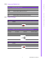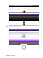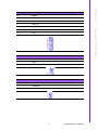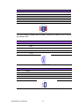
1
User Manual SOM-AB5510 Copyright The documentation and the software included with this product are copyrighted 2014 by Advantech Co., Ltd. All rights are reserved. Advantech Co., Ltd. reserves the right to make improvements in the products described in this manual at any time without notice. No part of this manual may be reproduced, copied, translated or transmitted in any form or by any means without the prior written permission of Advantech Co., Ltd. Information provided in this manual is intended to be accurate and reliable. However, Advantech Co., Ltd. assumes no responsibility for its use, nor for any infringements of the rights of third parties, which may result from its use. Acknowledgements Intel and Pentium are trademarks of Intel Corporation. Microsoft Windows and MS-DOS are registered trademarks of Microsoft Corp. All other product names or trademarks are properties of their respective owners. Product Warranty (2 years) Advantech warrants to you, the original purchaser, that each of its products will be free from defects in materials and workmanship for two years from the date of purchase. This warranty does not apply to any products which have been repaired or altered by persons other than repair personnel authorized by Advantech, or which have been subject to misuse, abuse, accident or improper installation. Advantech assumes no liability under the terms of this warranty as a consequence of such events. Because of Advantech’s high quality-control standards and rigorous testing, most of our customers never need to use our repair service. If an Advantech product is defective, it will be repaired or replaced at no charge during the warranty period. For outof-warranty repairs, you will be billed according to the cost of replacement materials, service time and freight. Please consult your dealer for more details. If you think you have a defective product, follow these steps: 1. Collect all the information about the problem encountered. (For example, CPU speed, Advantech products used, other hardware and software used, etc.) Note anything abnormal and list any onscreen messages you get when the problem occurs. 2. Call your dealer and describe the problem. Please have your manual, product, and any helpful information readily available. 3. If your product is diagnosed as defective, obtain an RMA (return merchandize authorization) number from your dealer. This allows us to process your return more quickly. 4. Carefully pack the defective product, a fully-completed Repair and Replacement Order Card and a photocopy proof of purchase date (such as your sales receipt) in a shippable container. A product returned without proof of the purchase date is not eligible for warranty service. 5. Write the RMA number visibly on the outside of the package and ship it prepaid to your dealer. SOM-AB5510 User Manual Part No. 2006551010 Edition 1 Printed in Taiwan July 2014 ii Declaration of Conformity CE This product has passed the CE test for environmental specifications. Test conditions for passing included the equipment being operated within an industrial enclosure. In order to protect the product from being damaged by ESD (Electrostatic Discharge) and EMI leakage, we strongly recommend the use of CE-compliant industrial enclosure products. FCC Class B Note: This equipment has been tested and found to comply with the limits for a Class B digital device, pursuant to part 15 of the FCC Rules. These limits are designed to provide reasonable protection against harmful interference in a residential installation. This equipment generates, uses and can radiate radio frequency energy and, if not installed and used in accordance with the instructions, may cause harmful interference to radio communications. However, there is no guarantee that interference will not occur in a particular installation. If this equipment does cause harmful interference to radio or television reception, which can be determined by turning the equipment off and on, the user is encouraged to try to correct the interference by one or more of the following measures: Reorient or relocate the receiving antenna. Increase the separation between the equipment and receiver. Connect the equipment into an outlet on a circuit different from that to which the receiver is connected. Consult the dealer or an experienced radio/TV technician for help. Technical Support and Assistance 1. 2. Visit the Advantech website at http://support.advantech.com where you can find the latest information about the product. Contact your distributor, sales representative, or Advantech's customer service center for technical support if you need additional assistance. Please have the following information ready before you call: – Product name and serial number – Description of your peripheral attachments – Description of your software (operating system, version, application software, etc.) – A complete description of the problem – The exact wording of any error messages iii SOM-AB5510 User Manual Warnings, Cautions and Notes Warning! Warnings indicate conditions, which if not observed, can cause personal injury! Caution! Cautions are included to help you avoid damaging hardware or losing data. e.g. There is a danger of a new battery exploding if it is incorrectly installed. Do not attempt to recharge, force open, or heat the battery. Replace the battery only with the same or equivalent type recommended by the manufacturer. Discard used batteries according to the manufacturer's instructions. Note! Notes provide optional additional information. Document Feedback To assist us in making improvements to this manual, we welcome comments and constructive criticism. Please send all such - in writing to: [email protected] Packing List Before setting up the system, check that the items listed below are included and in good condition. If any items are missing, please contact your dealer immediately. SOM-AB5510 Module 1x SOM-AB5510 (3.5” Application Board for COM-Express Mini module) 1x1700008894 (SATA Cable 7P 30CM) 1x1700018785 (SATA Power Cable 15P/1*4P-2.5 35CM) 1x1703100152 (Audio Cable 2*5P-2.0/JACK*3 20cm) SOM-AB5510 User Manual iv Safety Instructions 1. 2. 3. Read these safety instructions carefully. Keep this User Manual for later reference. Disconnect this equipment from any AC outlet before cleaning. Use a damp cloth. Do not use liquid or spray detergents for cleaning. 4. For plug-in equipment, the power outlet socket must be located near the equipment and must be easily accessible. 5. Keep this equipment away from humidity. 6. Put this equipment on a reliable surface during installation. Dropping it or letting it fall may cause damage. 7. The openings on the enclosure are for air convection. Protect the equipment from overheating. DO NOT COVER THE OPENINGS. 8. Make sure the voltage of the power source is correct before connecting the equipment to the power outlet. 9. Position the power cord so that people cannot step on it. Do not place anything over the power cord. 10. All cautions and warnings on the equipment should be noted. 11. If the equipment is not used for a long time, disconnect it from the power source to avoid damage by transient overvoltage. 12. Never pour any liquid into an opening. This may cause fire or electrical shock. 13. Never open the equipment. For safety reasons, the equipment should be opened only by qualified service personnel. 14. If one of the following situations arises, get the equipment checked by service personnel: The power cord or plug is damaged. Liquid has penetrated into the equipment. The equipment has been exposed to moisture. The equipment does not work well, or you cannot get it to work according to the user's manual. The equipment has been dropped and damaged. The equipment has obvious signs of breakage. 15. DO NOT LEAVE THIS EQUIPMENT IN AN ENVIRONMENT WHERE THE STORAGE TEMPERATURE MAY GO BELOW -20° C (-4° F) OR ABOVE 60° C (140° F). THIS COULD DAMAGE THE EQUIPMENT. THE EQUIPMENT SHOULD BE IN A CONTROLLED ENVIRONMENT. 16. CAUTION: DANGER OF EXPLOSION IF BATTERY IS INCORRECTLY REPLACED. REPLACE ONLY WITH THE SAME OR EQUIVALENT TYPE RECOMMENDED BY THE MANUFACTURER, DISCARD USED BATTERIES ACCORDING TO THE MANUFACTURER'S INSTRUCTIONS. The sound pressure level at the operator's position according to IEC 704-1:1982 is no more than 70 dB (A). DISCLAIMER: This set of instructions is given according to IEC 704-1. Advantech disclaims all responsibility for the accuracy of any statements contained herein. v SOM-AB5510 User Manual Safety Precaution - Static Electricity Follow these simple precautions to protect yourself from harm and the products from damage. To avoid electrical shock, always disconnect the power from your PC chassis before you work on it. Don't touch any components on the CPU card or other cards while the PC is on. Disconnect power before making any configuration changes. The sudden rush of power as you connect a jumper or install a card may damage sensitive electronic components. SOM-AB5510 User Manual vi Contents Chapter 1 General Information ............................1 1.1 1.2 Introduction ............................................................................................... 2 Connectors and Jumper Settings.............................................................. 3 1.2.1 Connector Location....................................................................... 3 Figure 1.1 Connector Location - Front side ................................. 3 Figure 1.2 Connector Location - Back side.................................. 3 1.2.2 I/O Connector Location ................................................................. 4 Figure 1.3 I/O Location-side ........................................................ 4 Figure 1.4 I/O Location-back ....................................................... 4 1.2.3 Button, Jumper and Switch location.............................................. 5 Figure 1.5 Button, Jumper and Switch location - Front side ........ 5 Figure 1.6 Button, Jumper and Switch location - Back side ........ 5 1.2.4 LED Location ................................................................................ 6 Figure 1.7 LED Location .............................................................. 6 1.2.5 Connector List............................................................................... 6 Table 1.1: Connector List ............................................................ 6 1.2.6 Jumper and Switch List................................................................. 7 Table 1.2: Jumper and Switch List .............................................. 7 1.2.7 Jumper Settings ............................................................................ 7 Table 1.3: (JUMP1) Selection Straps for LVDS Backlight Voltage .................................................................................... 7 Table 1.4: (JUMP2) Selection Straps for BIOS IC Boot Source .. 7 Table 1.5: (JRTC1) Clear COMS Jumper.................................... 7 Table 1.6: (PJUMP1) Selection Straps for AT/ATX Mode ........... 8 Table 1.7: (SW6) Selection Straps for Mini PCIe/mSATA Auto-detection ......................................................................... 8 1.2.8 Connector Pin Definition ............................................................... 8 Table 1.8: (JPS1) ATX 4 Pin 12 V in Connector.......................... 8 Table 1.9: (JPS2) Adapter 8.5V~20V in Connector..................... 8 Table 1.10: (JBAT1) Battery Connector ........................................ 9 Table 1.11: (JRTC2) Coin Battery Connector................................ 9 Table 1.12: (JPB1) Power Button Connector ................................ 9 Table 1.13: (JGPIO1) GPIO Pin Header ..................................... 10 Table 1.14: (JSMB1) SMBus Connector ..................................... 10 Table 1.15: (JI2C1) I2C Connector.............................................. 10 Table 1.16: (JLPC1) LPC Connector........................................... 11 Table 1.17: (JACK1) Line-in, Line-out and MIC Connector ......... 11 Table 1.18: (JFAN1) FAN Connector .......................................... 11 Table 1.19: (JFP1) Front Panel Pin Header ................................ 12 Table 1.20: (JLVDS1) LVDS Interface Connector ....................... 13 Table 1.21: (JLVDS2) LVDS Invertor Power Connector.............. 14 Table 1.22: (JSATA2) SATA 5V Power Connector ..................... 14 1.2.9 LED Instructions List .................................................................. 14 Table 1.23: LED Instructions List................................................. 14 Table 1.24: (LED7) DC IN Power Present / Absent..................... 15 Table 1.25: (LED8) 5V Standby Power Present / Absent............ 15 Table 1.26: (LED3) Sleep S3 Present / Absent ........................... 15 Table 1.27: (LED5) Sleep S4 Present / Absent ........................... 15 Table 1.28: (LED4) Sleep S5 Present / Absent ........................... 15 Table 1.29: (LED1) SATA data transfer Active / Inactive ............ 15 vii SOM-AB5510 User Manual SOM-AB5510 User Manual viii Chapter 1 1 General Information 1.1 Introduction SOM-AB5510 is an application board for COM-Express Mini Type 10 pin-out module with 3.5” form factor, which fully complies with the PCI Industrial Computer Manufactures PICMG COM Express standard. SOM-AB5510 has several popular features and rich I/O expansions, such as mSATA, USB3.0, USB Client, CAN Bus, Mini PCIe and more. In addition, SOM-AB5510 also supports wild voltage input (8.5~20V) and is compliant with Smart Battery Charger Specification V1.1 (SBS V1.1). All these features are designed to meet wide-ranged application of embedded products. Advantech also provides design reference for several features. Please contact your distributor, sales representative, or Advantech's customer service center for technical support. SOM-AB5510 User Manual 2 Chapter 1 1.2 Connectors and Jumper Settings 1.2.1 Connector Location JI2C1 SOM-AB1 JSATA1 JLVDS1 JSMB1 JLPC1 JSATA2 JLVDS2 JSDIO1 JBAT1 JPB1 JFAN1 JFP1 JPS1 JUSB2 JUSB3 JHDMI1 JLAN1 JCOM1 JSPI1 JUSB1 JPS2 JRTC2 Figure 1.1 Connector Location - Front side JMINI1 JSIM1 JMINI2 Figure 1.2 Connector Location - Back side 3 SOM-AB5510 User Manual General Information JGPIO1 JACK1 1.2.2 I/O Connector Location USB 2.0 PORT5 USB 2.0 PORT4 USB 3.0 PORT1 USB 3.0 PORT0 HDMI COM Port/ CAN Bus LAN USB Client Figure 1.3 I/O Location-side Mini PCIe Connector (Include USB2.0 Port2 and PCIe Port 0) Figure 1.4 I/O Location-back SOM-AB5510 User Manual 4 Mini PCIe Connector (Include USB2.0 Port3 and PCIe Port1) DC IN Chapter 1 1.2.3 Button, Jumper and Switch location JUMP1 LID Switch Sleep Button Reset Button Power Button JRTC1 JUMP2 Figure 1.5 Button, Jumper and Switch location - Front side SW6 Figure 1.6 Button, Jumper and Switch location - Back side 5 SOM-AB5510 User Manual General Information PJUMP1 1.2.4 LED Location DC IN Power LED 5V Standby Power LED Sleep S3 LED Sleep S4 LED Sleep S5 LED SATA data transfer LED Figure 1.7 LED Location 1.2.5 Connector List Table 1.1: Connector List Label Function JPS1 ATX 4 Pin 12 V in Connector JPS2 Adapter 8.5V~20V in connector SOM-AB1 COM Connector JUSB1 USB Client Connector JUSB2 USB2.0 Port 4 & 5 JUSB3 USB3.0 Port 0 & 1 JMINI1 Mini PCIe PORT 0 Connector (Include USB2.0 Port 2) JMINI2 Mini PCIe PORT 1 Connector (Include USB2.0 Port 3) JSIM1 SIM Card Socket JHDMI1 HDMI Connector JLVDS1 LVDS Interface Connector JLVDS2 LVDS Invertor Power Connector JSATA1 SATA Connector JSATA2 SATA 5V Power Connector JSDIO1 SDIO Connector JLPC1 LPC Connector JSMB1 SMBus Connector JI2C1 I2C Connector JGPIO1 GPIO Pin Header JPB1 Power Button Connector JBAT1 Battery Connector JRTC2 Coin Battery Connector JSPI1 SPI EEPROM Socket JFP1 Front Panel Pin Header JCOM1 COM Connector JACK1 Line-in, Line-out and MIC Connector JFAN1 FAN Connector JLAN1 LAN Connector SOM-AB5510 User Manual 6 Chapter 1 1.2.6 Jumper and Switch List Table 1.2: Jumper and Switch List Function JUMP1 Selection straps for LVDS Backlight Voltage JUMP2 Selection straps for BIOS IC boot source JRTC1 Clear COMS Jumper PJUMP1 Selection straps for AT/ATX Mode SW6 Selection straps for Mini PCIe/mSATA auto-detection 1.2.7 Jumper Settings Table 1.3: (JUMP1) Selection Straps for LVDS Backlight Voltage Pin Function 1-2 5V (Default) 2-3 3.3V Table 1.4: (JUMP2) Selection Straps for BIOS IC Boot Source J1 J2 SPI Descriptor Bios Entry No Jumper No Jumper COM SPI COM SPI (Default) 1-2 No Jumper COM SPI Carrier FWH No Jumper 3-4 Carrier SPI COM/Carrier SPI 1-2 3-4 COM SPI COM/Carrier SPI Table 1.5: (JRTC1) Clear COMS Jumper Pin Function 1-2 Clear CMOS 2-3 Normal Operation (Default) 7 SOM-AB5510 User Manual General Information Label Table 1.6: (PJUMP1) Selection Straps for AT/ATX Mode J3 J4 Power Mode 1-2 No Jumper AT POWER MODE No Jumper 3-4 ATX POWER MODE (Default) Table 1.7: (SW6) Selection Straps for Mini PCIe/mSATA Auto-detection S1 S2 Function ON OFF Auto-Detection (Default) OFF ON Mini PCIe OFF OFF mSATA ON ON Mini PCIe 1.2.8 Connector Pin Definition Table 1.8: (JPS1) ATX 4 Pin 12 V in Connector Pin Signal 1, 2 GND 3, 4 +VDC Table 1.9: (JPS2) Adapter 8.5V~20V in Connector Pin Signal 1 +VDC 2 GND SOM-AB5510 User Manual 8 Chapter 1 Table 1.10: (JBAT1) Battery Connector Signal 1, 2 +VDC 3 ID 4 SMB_CLK 5 SMB_DATA 6 THERMAL 7, 8 GND General Information Pin Table 1.11: (JRTC2) Coin Battery Connector Pin Signal 1 +VRTC 2 GND Table 1.12: (JPB1) Power Button Connector Pin Signal 1 PWRBTN# 2 GND 9 SOM-AB5510 User Manual Table 1.13: (JGPIO1) GPIO Pin Header Pin Signal Pin Signal 1 GPI0 6 GPO2* 2 GPO0 7 GPI3 3 GPI1 8 GPO3 4 GPO1 9 GND 5 GPI2 10 GND 1 3 5 7 9 JGPIO1 2 4 6 8 10 PH_5x2V_S2.54mm *GPO2 is used by charger alert in default. Optional to release GPO2 if removing charger alert. Table 1.14: (JSMB1) SMBus Connector Pin Signal 1 GND 2 SMB DATA 3 SMB CLOCK 4 +3.3V Table 1.15: (JI2C1) I2C Connector Pin Signal 1 GND 2 I2C DATA 3 I2C CLOCK 4 +3.3V 1 2 3 4 JI2C1 WB_4V_2.0mm SOM-AB5510 User Manual 10 Chapter 1 Table 1.16: (JLPC1) LPC Connector Signal Pin Signal 1 Clock 8 GND 2 LPC AD1 9 LPC AD2 3 PLTRST# 10 SMB Clock 4 LPC AD0 11 SERIRQ 5 LPC FRAME# 12 SMB DATA 6 +3.3V 13 +5V 7 LPC AD3 14 +5V 1 3 5 7 9 11 13 JLPC1 2 4 6 8 10 12 14 PH(F)_7x2V_2.00mm Table 1.17: (JACK1) Line-in, Line-out and MIC Connector Pin Signal Pin Signal 1 Right Line out 6 Left Line in 2 Right Line in 7 GND 3 GND 8 GND 4 GND 9 Right MIC in 5 Left Line out 10 Left MIC in Table 1.18: (JFAN1) FAN Connector Pin Signal 1 GND 2 +V_FAN 3 FANTACH 11 SOM-AB5510 User Manual General Information Pin Table 1.19: (JFP1) Front Panel Pin Header Pin Signal Pin Signal 1 NA 11 SATA LED 2 NA 12 Pull Up to +3.3V via 220 ohm 3 PWR LED 13 POWER BUTTON# 4 GND 14 GND 5 SPKR 15 NA 6 GND 16 NA 7 BUZZER 17 RESET BUTTON# 8 NA 18 GND 9 NA 19 Watch Dog LED 10 NA 20 GND Function Description PIN Function Description 3-4 Power LED Connector (Pin 3 is positive) For Power status LED 5-6 Buzzer Connector For external buzzer 5-7 Buzzer Jumper (Default) Enable on-board buzzer 11-12 SATA LED Connector (Pin 12 is positive) For SATA data transfer LED 13-14 Power Button Connector For power button 17-18 Reset Button Connector For system reset button 19-20 Watch Dog LED Connector (Pin 19 is positive) For watch dog timeout indication LED SOM-AB5510 User Manual 12 Chapter 1 Table 1.20: (JLVDS1) LVDS Interface Connector Signal Pin Signal 1 +LCDVDD 21 LVDS_D2+ 2 +LCDVDD 22 NA 3 GND 23 GND 4 GND 24 GND 5 +LCDVDD 25 LVDS_CLK- 6 +LCDVDD 26 NA 7 LVDS_D0- 27 LVDS_CLK+ 8 NA 28 NA 9 LVDS_D0+ 29 GND 10 NA 30 GND 11 GND 31 LVDS_DDC_CLK 12 GND 32 LVDS_DDC_DATA 13 LVDS_D1- 33 GND 14 NA 34 EDP_HDP 15 LVDS_D1+ 35 LVDS_D3- 16 NA 36 NA 17 GND 37 LVDS_D3+ 18 GND 38 NA 19 LVDS_D2- 39 Pull Down to ground via 4.7K ohm 20 NA 40 LVDS_CTRL 13 SOM-AB5510 User Manual General Information Pin Table 1.21: (JLVDS2) LVDS Invertor Power Connector Pin Signal 1 +5V 2 GND 3 LVDS Back Light Enable 4 Back Light Control 5 +5V Table 1.22: (JSATA2) SATA 5V Power Connector 1.2.9 Pin Signal 1 +5V 2 GND 3 NA 4 NA LED Instructions List Table 1.23: LED Instructions List LED Indication LED7 DC IN Power Present / Absent LED8 5V Standby Power Present / Absent LED3 Sleep S3 Present / Absent LED5 Sleep S4 Present / Absent LED4 Sleep S5 Present / Absent LED1 SATA data transfer Active / Inactive SOM-AB5510 User Manual 14 LED Signal Light Dark Description DC IN Power Present DC IN Power Absent Chapter 1 Table 1.24: (LED7) DC IN Power Present / Absent Table 1.25: (LED8) 5V Standby Power Present / Absent Light Dark Description 5V Standby Power Present 5V Standby Power Absent Table 1.26: (LED3) Sleep S3 Present / Absent LED Signal Light Dark Description Sleep S3 Present Sleep S3 Absent Table 1.27: (LED5) Sleep S4 Present / Absent LED Signal Light Dark Description Sleep S4 Present Sleep S4 Absent Table 1.28: (LED4) Sleep S5 Present / Absent LED Signal Light Dark Description Sleep S5 Present Sleep S5 Absent Table 1.29: (LED1) SATA data transfer Active / Inactive LED Signal Glisten Dark Description SATA data transfer Active SATA data transfer Inactive 15 SOM-AB5510 User Manual General Information LED Signal www.advantech.com Please verify specifications before quoting. This guide is intended for reference purposes only. All product specifications are subject to change without notice. No part of this publication may be reproduced in any form or by any means, electronic, photocopying, recording or otherwise, without prior written permission of the publisher. All brand and product names are trademarks or registered trademarks of their respective companies. © Advantech Co., Ltd. 2014