1
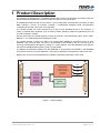
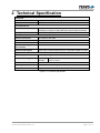
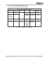
The Embedded I/O Company
TIP302
Multiprotocol Communication IP
(based on MC68302)
Version 1.0
User Manual
Issue 1.5
October 2008
TEWS TECHNOLOGIES GmbH
Am Bahnhof 7
Phone: +49-(0)4101-4058-0
25469 Halstenbek, Germany
Fax: +49-(0)4101-4058-19
www.tews.com
e-mail: [email protected]
TEWS TECHNOLOGIES LLC
9190 Double Diamond Parkway,
Suite 127, Reno, NV 89521, USA
www.tews.com
Phone: +1 (775) 850 5830
Fax: +1 (775) 201 0347
e-mail: [email protected]
TIP302-12
Multiprotocol Communication IP
(based on MC68302)
This document contains information, which is
proprietary to TEWS TECHNOLOGIES GmbH. Any
reproduction without written permission is forbidden.
TEWS TECHNOLOGIES GmbH has made any
effort to ensure that this manual is accurate and
complete. However TEWS TECHNOLOGIES GmbH
reserves the right to change the product described
in this document at any time without notice.
TEWS TECHNOLOGIES GmbH is not liable for any
damage arising out of the application or use of the
device described herein.
© 2002-2008 by TEWS TECHNOLOGIES GmbH
All trademarks mentioned are property of their respective owners.
TIP302 User Manual Issue 1.5
Page 2 of 21
Issue
Description
Date
1.0
Initial Issue
January 2002
1.1
General Revision
February 2002
1.2
Correction of Base Value in Basic Code Example
March 2002
1.3
New address TEWS LLC
September 2006
1.4
Supplement to Technical Specification
September 2007
1.5
Added weight to Technical Specification table
October 2008
TIP302 User Manual Issue 1.5
Page 3 of 21
Table of Contents
1
2
3
4
PRODUCT DESCRIPTION ......................................................................................... 6
TECHNICAL SPECIFICATION................................................................................... 7
ID PROM CONTENT .................................................................................................. 8
ADDRESS MAPS ....................................................................................................... 9
4.1 IP Bus Address Map .......................................................................................................................9
4.1.1 I/O Space Addressing ..........................................................................................................9
4.1.1.1 Reset Register............................................................................................................10
4.1.1.2 Interrupt Request Register .........................................................................................11
4.1.1.3 Interrupt Vector Register ............................................................................................12
4.1.1.4 Memory Enable Register ............................................................................................13
4.1.2 Memory Space Addressing ................................................................................................13
4.2 Local Bus Address Map ...............................................................................................................14
4.2.1 On board SRAM.................................................................................................................14
4.2.2 MC68302 System Block.....................................................................................................14
4.2.3 Interrupt Register ...............................................................................................................15
4.2.3.1 Interrupt Vector Register ............................................................................................15
4.2.3.2 Interrupt Request Register .........................................................................................15
4.2.4 Local Bus Address Map Example ......................................................................................16
5
PROGRAMMING ...................................................................................................... 17
5.1 IP Host CPU ...................................................................................................................................17
5.2 MC68302 Program Code...............................................................................................................17
5.2.1 Basic Code Example..........................................................................................................18
5.3 Getting Started ..............................................................................................................................19
6
I/O PIN ASSIGNMENT ............................................................................................. 20
TIP302 User Manual Issue 1.5
Page 4 of 21
Table of Figures
FIGURE 1-1: BLOCK DIAGRAM......................................................................................................................... 6
FIGURE 2-1: TECHNICAL SPECIFICATION...................................................................................................... 7
FIGURE 3-1: TIP302-12 V1.0 ID PROM CONTENTS ........................................................................................ 8
FIGURE 4-1: I/O SPACE REGISTERS............................................................................................................... 9
FIGURE 4-2: RESET REGISTER ..................................................................................................................... 10
FIGURE 4-3: INTERRUPT REQUEST REGISTER .......................................................................................... 11
FIGURE 4-4: INTERRUPT VECTOR REGISTER............................................................................................. 12
FIGURE 4-5: MEMORY ENABLE REGISTER.................................................................................................. 13
FIGURE 4-6 : LOCAL BUS ADDRESS MAP EXAMPLE .................................................................................. 16
FIGURE 6-1: I/O PIN ASSIGNMENT ................................................................................................................ 21
TIP302 User Manual Issue 1.5
Page 5 of 21
1 Product Description
The TIP302 is an IndustryPack® compatible module with a serial communication I/O interface using the
Motorola MC68302 Multiprotocol Communication Processor running at 25 MHz.
The MC68302 contains a 68K core processor, a micro-coded RISC communication processor, 6 serial
DMA channels, 3 timers, an interrupt controller, 3 independent full-duplex serial communication
controllers (SCCs) and 1152 bytes of on-chip RAM.
The TIP302 provides TTL level interface for all 3 SCC’s of the MC68302 at the IP I/O connector. A
variety of physical layer standards, such as RS232, RS422, RS485 or ISDN are supported by the use
of custom transition modules.
Internal microcode in the 68302 supports a variety of protocols, such as BISYNC, HDLC, SDLC, UART,
DDCMP, V.110, ISDN (2B+D) and transparent modes.
The TIP302 provides 1 Mbyte (512 Kbit x 16) of static RAM (SRAM) as dual-port memory for both,
MC68302 code and user data. The code is downloaded to the SRAM by the IP host CPU prior to
removing the MC68302 reset signal by writing to a control register. Once the MC68302 reset signal is
removed, the MC68302 starts fetching code from the SRAM.
The SRAM, the MC68302 registers and the MC68302 on-chip RAM are accessible by the MC68302
and by the IP host CPU through arbitration. The local bus arbitration is transparent to the IP host CPU.
Both the IP host CPU and the MC68302 are capable of generating interrupts to each other.
MC68302
FPGA
IP-Local
Interface
Register
ID-PROM
Multiprotocol
Communication
Processor
(25MHz)
SRAM
512Kbit x 16
Ch2
Ch3
GPIO
IndustryPack I/O Interface
IndustryPack logic Interface
Ch1
Figure 1-1: Block Diagram
TIP302 User Manual Issue 1.5
Page 6 of 21
2 Technical Specification
IP Interface
IP Interface
Single Size IndustryPack® Logic Interface
On board Devices
Processor
Motorola MC68302-PV (25 MHz)
Including 1152 byte on-chip RAM and Communication Processor
Memory
512 Kbit x 16 (1Mbyte) SRAM
I/O Interface
Interface Connector
50-conductor flat cable
Number of Serial Channels
3
Interface
TTL level interface for all 3 SCC’s
Serial Channel Signals
(per Channel)
RXD, TXD, RCLK, TCLK, CD, CTS, RTS, BRG
Additional I/O Signals
Timer Input, Interrupt Request Input, 4 General Purpose I/O Lines
Physical Data
Power Requirements
115mA typical @ + 5V DC
Temperature Range
Operating
Storage
MTBF
219183 h
Humidity
5 – 95 % non-condensing
Weight
27g
0 °C to +70 °C
-40°C to +85 °C
Figure 2-1: Technical Specification
TIP302 User Manual Issue 1.5
Page 7 of 21
3 ID PROM Content
ID_PROM CONTENT
Address
Function
Content
01h
ASCII ‘I’
49h
03h
ASCII ‘P’
50h
05h
ASCII ‘A’
41h
07h
ASCII ‘C’
43h
09h
Manufacturer ID
B3h
0Bh
Model Number
32h
0Ch
Revision
10h
0Fh
RESERVED
00h
11h
Driver-ID Low-Byte
00h
13h
Driver-ID High-Byte
00h
15h
Number of bytes used
0Ch
17h
CRC
1Eh
Figure 3-1: TIP302-12 V1.0 ID PROM Contents
TIP302 User Manual Issue 1.5
Page 8 of 21
4 Address Maps
4.1 IP Bus Address Map
The IP host CPU can access:
• Control/Status Registers in the IP I/O space
• 1 Mbyte on board SRAM in the IP memory space
(If MC68302 is in total-reset or if MC68302 is running and configured)
• MC68302 basic registers (BAR, SCR, CKCR) in the IP memory space
(If MC68302 is running)
• MC68302 4K system block in the IP memory space
(If MC68302 is running and configured)
4.1.1 I/O Space Addressing
The TIP302 provides four 8-bit wide registers accessible in the IP I/O space.
I/O SPACE REGISTERS
Register Name
Register
Symbol
Size
Address
Reset Register
RST_REG
8-bit
01h
Interrupt Request Register
IRQ_REG
8-bit
03h
Interrupt Vector Register
VEC_REG
8-bit
05h
Memory Enable Register
MEN_REG
8-bit
07h
Figure 4-1: I/O Space Registers
TIP302 User Manual Issue 1.5
Page 9 of 21
4.1.1.1 Reset Register
RESET REGISTER
Bit Number
Bit Symbol
Access
Description
7
(MSB)
-
-
1
HALT#
R/W
0 : Assert local bus HALT#
signal (reset value)
1 : De-assert local bus HALT#
signal
0
(LSB)
RESET#
R/W
0 : Assert local bus RESET#
signal (reset value)
1 : De-assert local bus
RESET# signal
Reads : Always 0b
Writes : No effect
6
5
4
3
2
Figure 4-2: Reset Register
The Reset Register is used to hold the MC68302 in a state called total-reset, where the MC68302 is
stopped from executing or fetching program code.
If both the HALT# and RESET# bits are clear (reset value), the MC68302 is held in the total-reset state.
If both the HALT# and RESET# bits are set, the MC68302 is running.
After power up or IP reset the MC68302 is held in the total-reset state.
The IP host CPU then can download program code to the on board SRAM.
After that, the IP host CPU can release the MC68302 by setting both the HALT# and RESET# bits (i.e.
writing 03h to the Reset Register).
Then the MC68302 starts fetching program code from the reset vector address.
(1)
The HALT# and the RESET# bit should always be set to identical bit values.
The user should either write 00h or 03h to the Reset Register.
TIP302 User Manual Issue 1.5
Page 10 of 21
4.1.1.2 Interrupt Request Register
INTERRUPT REQUEST REGISTER
Bit Number
Bit Symbol
Access
Description
7
(MSB)
-
-
2
IRQ1
R/S
Reads :
0 : No pending interrupt
request
1 : Pending interrupt request
Writes:
0 : No effect
1 : Generate MC68302 level 1
interrupt request
1
IRQ6
R/S
Reads :
0 : No pending interrupt
request
1 : Pending interrupt request
Writes:
0 : No effect
1 : Generate MC68302 level 6
interrupt request
0
(LSB)
IRQ7
R/S
Reads :
0 : No pending interrupt
request
1 : Pending interrupt request
Writes:
0 : No effect
1 : Generate MC68302 level 7
interrupt request
Reads : Always 0b
Writes : No effect
6
5
4
3
Figure 4-3: Interrupt Request Register
The Interrupt Request Register is used to generate interrupt requests to the MC68302.
The MC68302 must be configured to use the dedicated operational interrupt mode with auto-vectored
level sensitive interrupts.
The IP host CPU can generate interrupt requests to the MC68302 by writing 1b to the appropriate IRQ
bit in the Interrupt Request Register. Interrupt levels 1, 6, and 7 are available.
The IP host CPU can check the interrupt request status by reading the Interrupt Request Register. If an
IRQ bit is set to 1b, the interrupt request is still pending. Cleared IRQ bits indicate that the interrupt
request has been acknowledged by the MC68302.
TIP302 User Manual Issue 1.5
Page 11 of 21
The IRQ bits in the Interrupt Request Register are cleared by hardware during the MC68302 interrupt
acknowledge cycle.
Asserting a total-reset to the MC68302 will also clear the Interrupt Request Register.
The reset value of the Interrupt Request Register is 00h.
(1)
Prior setting an IRQ bit in the Interrupt Request Register, the user has to check that the IRQ bit
is clear.
4.1.1.3 Interrupt Vector Register
INTERRUPT VECTOR REGISTER
Bit Number
Bit Symbol
Access
Description
7
(MSB)
VEC_BYTE
R/W
Interrupt Vector for IP Host
CPU.
6
5
4
3
2
1
0
(LSB)
Figure 4-4: Interrupt Vector Register
The Interrupt Vector Register contains the interrupt vector for interrupts to the IP host CPU.
A write cycle is the only source which can generate an IP host CPU interrupt request to an Interrupt
Request Register in the local bus address map.
Only the IP INT0 interrupt channel is used. The IP INT1 interrupt channel is unused.
The Interrupt Vector Register can also be mapped to the local bus address map. Then it is accessible
on the local bus by both the IP host CPU and the MC68302.
The reset value of the Interrupt Vector Register is FFh.
Asserting a total-reset to the local CPU does not alter the content of the Interrupt Vector Register.
(1)
There is no arbitration between local bus writes and IP I/O Space writes to the Interrupt Vector
Register.
If the Interrupt Vector Register is written on both the local bus and in the IP I/O space, each write
to the Interrupt Vector Register should be verified by a read.
TIP302 User Manual Issue 1.5
Page 12 of 21
4.1.1.4 Memory Enable Register
MEMORY ENABLE REGISTER
Bit Number
Bit Symbol
Access
Description
7
(MSB)
MEN_BYTE
R/W
Must be set to value ADh to
enable IP Memory space
accesses, if on board jumper
is not installed.
6
5
4
Meaningless, if on board
jumper is installed.
3
2
1
0
(LSB)
Figure 4-5: Memory Enable Register
If the on board jumper is installed, the Memory Enable Register is meaningless.
If the on board jumper is not installed, the Memory Enable Register must be written with the value ADh
to enable IP memory space accesses. For other values the TIP302 will not acknowledge any IP
memory space access.
The reset value of the Memory Enable Register is 00h.
4.1.2 Memory Space Addressing
In IP memory space the IP host CPU can access the MC68302 basic registers (BAR, SCR, CKCR), the
MC68302 4K system block (on-chip RAM and internal registers) and the on board SRAM.
After power-up or IP reset or when the MC68302 is held in the total-reset state, all IP memory space
accesses will be directed to the on board SRAM.
When the MC68302 is taken out of the total-reset state, IP memory space accesses will address the
local bus address map as configured by the MC68302 chip select logic.
There is no address translation for IP memory space accesses to the local bus. The IP memory
address is directly transferred to the local bus.
The local bus arbitration is a hardware function and is transparent to the IP host CPU.
If the IP host CPU is the local bus master, the local bus A23 address line is always driven to A23 = 0.
As well, the local bus function code lines are driven to FC[2:0] = 101 (Supervisor Data) for local
addresses 0000FXh (MC68302 basic registers BAR, SCR, CKCR), and to FC[2:0] = 110 (Supervisor
Program) for all other local addresses.
TIP302 User Manual Issue 1.5
Page 13 of 21
4.2 Local Bus Address Map
The local bus address map consists of three main address regions.
• 1 Mbyte on board SRAM (zero-based, includes MC68302 Exception Vector Table)
• 4 Kbyte MC68302 system block (includes MC68302 on-chip RAM and internal registers)
• Local bus accessible interrupt registers
The local bus address map is configured by the program code in the on board SRAM. It programs the
MC68302 basic registers (BAR, SCR) and the MC68302 chip select logic registers (OR0, BR0, OR1,
BR1, OR3, BR3).
4.2.1 On board SRAM
The on board SRAM size is 1 Mbyte (512 Kbit x 16) and must be mapped to the address range 0h FFFFFh.
The chip select signals CS0 and CS1 of the MC68302 chip select logic are used for the on board
SRAM.
The CS0 chip select signal must be used and based to address 0h, so that it includes the MC68302
exception vector table (initial stack pointer, reset vector, etc.) and the initial program code section.
The remaining SRAM addresses can be split between the CS0 and CS1 chip select signal.
It is recommended to use the CS0 chip select signal for the code section and the CS1 chip select signal
for the data section.
For the MC68302 CS0 and CS1 chip select signals, internally generated DTACK with 6, 5, 4, 3, 2 or 1
wait states must be used. Internally generated DTACK with no wait-state or externally generated
DTACK options are not allowed.
IP reset or MC68302 total-reset do not alter the SRAM content.
4.2.2 MC68302 System Block
The base address of the MC68302 system block is defined by the MC68302 BAR register (word at
address 0F2h in supervisor data space). The MC68302 system block size is 4K. It resides at local bus
address range Base (BAR) - Base (BAR) + Fifth.
The MC68302 4K system block is divided into three sections:
• System RAM at base (BAR) + 0h (576 byte usable)
• Parameter RAM at base (BAR) + 400h (576 byte usable)
• Internal Registers at base (BAR) + 800h
The SAM bit and the EMWS bit in the MC68302 SCR register (long word at address 0F4h in supervisor
data space) must be cleared by the program code for proper IP host CPU access to the MC68302
system block.
TIP302 User Manual Issue 1.5
Page 14 of 21
4.2.3 Interrupt Register
Chip select signal CS3 of the MC68302 chip select logic is used for the local bus accessible interrupt
registers.
For the MC68302 CS3 chip select signal, internally generated DTACK with 6, 5, 4, 3, 2 or 1 wait states
must be used. Internally generated DTACK with no wait-state or externally generated DTACK options
are not allowed.
There are two 8-bit wide interrupt registers accessible on the local bus:
Base (CS3) + 01h: Interrupt Vector Register
Base (CS3) + 03h: Interrupt Request Register (IP host CPU Interrupt)
4.2.3.1 Interrupt Vector Register
This is the same Interrupt Vector Register, which is accessible by the IP host CPU in the IP I/O space.
A byte write to the Interrupt Vector Register at address base (CS3) + 01h must be performed to set the
IP bus interrupt vector.
A byte read from the Interrupt Vector Register at address base (CS3) + 01h must be performed to read
the actual IP bus interrupt vector.
(1)
The content of the Interrupt Vector Register may be overwritten by the IP host CPU in the IP I/O
space.
4.2.3.2 Interrupt Request Register
The Interrupt Request Register is used to generate an interrupt request on the IP bus.
Only the IP INT0 interrupt channel is used. The IP INT1 interrupt channel is unused.
A byte write to the Interrupt Request Register bit at address base (CS3) + 03h must be performed to
generate an interrupt request on the IP bus. The write data is meaningless.
If the actual or any previous interrupt request is still pending, the interrupt request status can be
checked by performing a byte read from address base (CS3) + 03h. Data line D0 indicates the status. If
D0 is read as Low there is no pending interrupt request. If D0 is read as High an interrupt request is
pending.
The Interrupt Request Register bit is cleared by hardware during the IP interrupt acknowledge cycle or
by IP reset.
(1)
Prior writing to the Interrupt Request Register the user has to check that the Interrupt Request
Register bit is clear.
TIP302 User Manual Issue 1.5
Page 15 of 21
4.2.4 Local Bus Address Map Example
The figure below shows a local bus address map example:
LOCAL BUS ADDRESS MAP EXAMPLE
Start
Address
End
Address
Size
Description
Access
Configuration
Register
0h
End of Code
Section
1Mbyte
SRAM
Code Section
MC68302 &
IP Host CPU
CS0 (BR0,
OR0)
Start of Data
Section
( = End of
Code Section
+ 1)
FFFFFh
SRAM
Data Section
MC68302 &
IP Host CPU
CS1 (BR1,
OR1)
100000h
101FFFh
8Kbyte
Interrupt
Register
MC68302 &
IP Host CPU
CS3 (BR3,
OR3)
102000h
102FFFh
4Kbyte
MC68302
System Block
(Including onchip RAM and
Internal
Registers)
MC68302 &
IP Host CPU
BAR
Figure 4-6 : Local Bus Address Map Example
TIP302 User Manual Issue 1.5
Page 16 of 21
5 Programming
5.1 IP Host CPU
After power-up the MC68302 is held in the total-reset state.
Then all IP memory space accesses are directed to the (zero-based) on board SRAM.
So after power-up the TIP302 is ready for downloading the MC68302 program code to the on board
SRAM.
The lowest address that can be used for the first command is address 400h, the address just above the
MC68302 exception vector table.
Besides downloading the program code, the IP host CPU must also set-up the initial SSP (long word at
address 000h) and the initial PC (long word at address 004h).
After that, the IP host CPU can get the MC68302 running by writing 03h to the Reset Register at
address 00h in the IP I/O space.
5.2 MC68302 Program Code
The MC68302 program should first mask off interrupts by programming the MC68302 SR register.
Then the MC68302 program code has to program:
the MC68302 BAR register (word at address 0F2h), to set the base address for the MC68302 4K
system block,
the MC68302 SCR register (long word at address 0F4h), to clear the SAM bit and the EMWS bit and
the MC68302 chip select registers in the following order: OR0, BR0, OR1, BR1, OR3, and BR3.
CS0 must be used for zero-based SRAM addresses, so the CS0 base address must be 0h.
CS0 is intended to be used for the code section so it can be configured to check for function code
supervisor program and to operate for reads only.
If CS1 is used for the SRAM data section, it has not to be configured to check the function code and to
operate for read and write operation.
If CS3 is used for the local bus interrupt register, it has not to be configured to check the function code
and to operate for read and write operation.
DTACK has to be programmed for internal DTACK generation with 1 wait-state for all CS0, CS1 and
CS3.
External DTACK or internal generated DTACK with no wait-state are not allowed to be used.
If interrupt requests to the MC68302 are used, the GIMR register must be programmed for: dedicated
interrupt mode, external (auto-) vector, level sensitive.
TIP302 User Manual Issue 1.5
Page 17 of 21
5.2.1 Basic Code Example
* Parameters and Registers
BASE
EQU
$102000
BAR
EQU
$0F2
SCR
EQU
$0F4
BR0
EQU
BASE+$0830
OR0
EQU
BASE+$0832
BR1
EQU
BASE+$0834
OR1
EQU
BASE+$0836
BR3
EQU
BASE+$083C
OR3
EQU
BASE+$083E
*
* Code Start Address
ORG
$00000400
*
* Status Register
*
Supervisor Mode
*
Mask Off Interrupts
MOVE.W
#$2700,SR
*
* Base Address Register
*
Base Address of 4K System Block = $102000
MOVE.W
#$0102,BAR
*
* System Control Register
* SAM = 0, EMWS = 0
MOVE.L
#0,SCR
*
* Chip Select 0
*
0h - 7FFFFh (512Kbyte)
*
1 WS
*
FC[2:0] = 110 (Supervisor Program)
*
Read Operation Only
MOVE.W
#$3F03,OR0
MOVE.W
#$C001,BR0
*
* Chip Select 1
*
80000h - FFFFFh (512Kbyte)
*
1 WS
*
Function Code Ignored
*
Read and Write Operation
MOVE.W
#$3F00,OR1
MOVE.W
#$C101,BR1
*
* Chip Select 3
*
100000h - 101FFFh (8Kbyte)
*
1 WS
*
Function Code Ignored
*
Read and Write Operation
MOVE.W
#$3FFC,OR3
MOVE.W
#$C201,BR3
*
TIP302 User Manual Issue 1.5
Page 18 of 21
* Write $FC to Interrupt Vector Register
MOVE.B
#$FC,$100001
*
* Write $ABCD to CS1 Block
LOOP
MOVE.W
#$ABCD,$80000
* Store same value to on-chip RAM
MOVE.W
$80000,$102000
* Loop
BRA.W
LOOP
During the MC68302 is busy executing this code, the IP host CPU can access:
• Program code at address range 0h - 7FFFFh as read only
• Program data at address range 80000h - FFFFFh as read / write
• MC68302 basic registers (BAR, SCR) at address range 0F2h and 0F4h
• MC68302 registers and on-chip RAM at address range 102000h - 102FFFh
• Interrupt Vector Register at byte address 100001h
(1)
In the code example above, an 8 Mbyte IP memory space is assumed.
For smaller IP memory space configurations it may be necessary to mask the higher address
lines in the MC68302 base or option registers.
5.3 Getting Started
CAUTION:
The component is an Electrostatic Sensitive Device (ESD). Use an anti-static mat connected to a
wristband when handling or installing the components.
1. Install the TIP302 on board jumper and power-up the TIP302 on an IP slot, enabled for 8 Mbyte of
IP memory space
2. Download the Basic Code Example of section 5.2.1 into the TIP302 SRAM, beginning at address
000400h.
As an alternative the code can be directly assembled to address 000400h.
3. Use the debugger, to write long words USP = 000F0000h to address 000000h and PC = 00000400h
to address 000004h.
4. Remove reset from the MC68302 by writing 03h to IP I/O address 01h (Reset Register). After that
the MC68302 will begin code fetching and execution.
5. Use the debugger, to read addresses 080000h (SRAM Data Section) and 102000h (MC68302 onchip RAM) and verify the value $ABCD. Write data to address 080002h (SRAM Data Section) and
read it back.
TIP302 User Manual Issue 1.5
Page 19 of 21
6 I/O Pin Assignment
All serial I/O lines of the MC68302 are routed directly (TTL level) to the local IP I/O connector.
I/O PIN ASSIGNMENT
I/O Pin Number
I/O Signal
MC68302 Pin Number
(144-Pin TQFP)
1
RXD1 / L1RXD
71
2
GND
3
TXD1 / L1TXD
4
GND
5
RCLK1 / L1RCLK
6
GND
7
TCLK1 / L1SY0 / SDS1
8
GND
9
CD1 / L1SY1
10
GND
11
CTS1 / L1GR
12
GND
13
RTS1 / L1RQ / GCIDCL
14
GND
15
BRG1 /
16
GND
17
RXD2 / PA0
18
GND
19
TXD2 / / PA1
20
GND
21
RCLK2 / PA2
22
GND
23
TCLK2 / PA3
24
GND
25
CTS2 / PA4
64
26
RTS2 / PA5
63
27
CD2 / PA6
62
28
BRG2 / SDS2 / PA7
61
29
GND
30
RXD3 / PA8
31
GND
32
TXD3 / PA9
TIP302 User Manual Issue 1.5
41
39
40
73
72
42
45
70
69
68
67
59
58
Page 20 of 21
I/O PIN ASSIGNMENT
I/O Pin Number
I/O Signal
MC68302 Pin Number
(144-Pin TQFP)
33
GND
34
RCLK3 / PA10
35
GND
36
TCLK3 / PA11
37
GND
38
CTS3 / SPRXD
74
39
RTS3 / SPTXD
43
40
CD3 / SPCLK
44
41
BRG3 / PA12
53
42
GND
43
TIN1 / PB3
44
GND
45
IRQ1
46
GND
47
PB8
142
48
PB9
141
49
PB10
140
50
PB11
139
57
56
6
Figure 6-1: I/O Pin Assignment
TIP302 User Manual Issue 1.5
Page 21 of 21