1
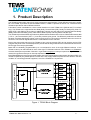
TIP866 8 Channel Serial Interface IP Version 1.0 Revision B User Manual Issue 1.2 18 December 1996 D75866802 TEWS DATENTECHNIK GmbH Am Bahnhof 7 D-25469 Halstenbek Germany Tel +49 (0)4101 4058-0 Fax +49 (0)4101 4058-19 7,3 8VHU 0DQXDO 9HUVLRQ TIP866-10 8 channel RS232 serial I/O TIP866-11 8 channel TTL serial I/O TIP866-20 8 channel RS422 serial I/O This manual covers all products This document contains information, which is proprietary to TEWS DATENTECHNIK GmbH. Any reproduction without written permission is forbidden. TEWS DATENTECHNIK GmbH has made any effort to ensure that this manual is accurate and complete. However TEWS DATENTECHNIK GmbH reserves the right to change the product described in this document at any time without notice. This product has been designed to operate with IndustryPackX compatible carriers. Connection to incompatible hardware is likely to cause serious damage. TEWS DATENTECHNIK GmbH is not liable for any damage arising out of the application or use of the device described herin. Issue Description Date 1.0 1.1 1.2 First issue Revision B Add RS422 Interface 29 August 1996 06 December 1996 18 December 1996 K1996 by TEWS DATENTECHNIK GmbH IndustryPack is a registered trademark of GreenSpring Computers, Inc 7,3 8VHU 0DQXDO 9HUVLRQ 1. Product Description . . . . . . . . . . . . . . . . . . . . . . . . . . . . . . . 5 2. Technical Specification . . . . . . . . . . . . . . . . . . . . . . . . . . . . . 6 3. ID Prom Contents . . . . . . . . . . . . . . . . . . . . . . . . . . . . . . . . . . 7 3.1. ID PROM Contents TIP866-xx V1.0 . . . . . . . . . . . . . . . . . . . . . . . . . 3.2. ID PROM Contents TIP866 Model Dependent . . . . . . . . . . . . . . . . 7 7 4. IP Addressing . . . . . . . . . . . . . . . . . . . . . . . . . . . . . . . . . . . . . . 8 4.1. TIP866 Register Map . . . . . . . . . . . . . . . . . . . . . . . . . . . . . . . . . . . . . 4.1.1. Register Set Channel 1 . . . . . . . . . . . . . . . . . . . . . . . . . . . . . . . . . . . 4.1.2. Register Set Channel 2 . . . . . . . . . . . . . . . . . . . . . . . . . . . . . . . . . . 4.1.3. Register Set Channel 3 . . . . . . . . . . . . . . . . . . . . . . . . . . . . . . . . . . . 4.1.4. Register Set Channel 4 . . . . . . . . . . . . . . . . . . . . . . . . . . . . . . . . . . . 4.1.5. Register Set Channel 5 . . . . . . . . . . . . . . . . . . . . . . . . . . . . . . . . . . 4.1.6. Register Set Channel 6 . . . . . . . . . . . . . . . . . . . . . . . . . . . . . . . . . . 4.1.7. Register Set Channel 7 . . . . . . . . . . . . . . . . . . . . . . . . . . . . . . . . . . 4.1.8. Register Set Channel 8 . . . . . . . . . . . . . . . . . . . . . . . . . . . . . . . . . . 4.2. Special Registers . . . . . . . . . . . . . . . . . . . . . . . . . . . . . . . . . . . . . . . . . 4.2.1. Interrupt Vector Register Address $0F . . . . . . . . . . . . . . . . . . . . . 4.2.2. FIFO Ready Status Register Channel 1-4 Address $1F . . . . . . 4.2.3. FIFO Ready Status Register Channel 5-8 Address $5F . . . . . . 9 9 10 11 12 13 14 15 16 17 17 18 19 5. Baud Rate Programming . . . . . . . . . . . . . . . . . . . . . . . . . . . . 20 5.1. Baud Rate Programming Formula . . . . . . . . . . . . . . . . . . . . . . . . . . . 20 6. I/O Pin Assignment . . . . . . . . . . . . . . . . . . . . . . . . . . . . . . . . . 21 6.1. 50 Pin I/O Connector TIP866-1x RS232/TTL . . . . . . . . . . . . . . . . . 6.2. 50 Pin I/O Connector TIP866-20 RS422 . . . . . . . . . . . . . . . . . . . . 21 22 7,3 8VHU 0DQXDO 9HUVLRQ Figure 1: TIP866 Block Diagram . . . . . . . . . . . . . . . . . . . . . . . . . . . . . . . . . Table 1: ID PROM Contents . . . . . . . . . . . . . . . . . . . . . . . . . . . . . . . . . . . . Table 2: ID PROM Contents Model Dependent . . . . . . . . . . . . . . . . . . . . Table 3: TIP866 I/O Address Map . . . . . . . . . . . . . . . . . . . . . . . . . . . . . . . Table 4: Register Set 1 Channel 1 . . . . . . . . . . . . . . . . . . . . . . . . . . . . . . . Table 5: Register Set 2 Channel 1 . . . . . . . . . . . . . . . . . . . . . . . . . . . . . . . Table 6: Register Set 1 Channel 2 . . . . . . . . . . . . . . . . . . . . . . . . . . . . . . . Table 7: Register Set 2 Channel 2 . . . . . . . . . . . . . . . . . . . . . . . . . . . . . . . Table 8: Register Set 1 Channel 3 . . . . . . . . . . . . . . . . . . . . . . . . . . . . . . . Table 9: Register Set 2 Channel 3 . . . . . . . . . . . . . . . . . . . . . . . . . . . . . . . Table 10: Register Set 1 Channel 4 . . . . . . . . . . . . . . . . . . . . . . . . . . . . . . Table 11: Register Set 2 Channel 4 . . . . . . . . . . . . . . . . . . . . . . . . . . . . . . Table 12: Register Set 1 Channel 5 . . . . . . . . . . . . . . . . . . . . . . . . . . . . . . Table 13: Register Set 2 Channel 5 . . . . . . . . . . . . . . . . . . . . . . . . . . . . . . Table 14: Register Set 1 Channel 6 . . . . . . . . . . . . . . . . . . . . . . . . . . . . . . Table 15: Register Set 2 Channel 6 . . . . . . . . . . . . . . . . . . . . . . . . . . . . . . Table 16: Register Set 1 Channel 7 . . . . . . . . . . . . . . . . . . . . . . . . . . . . . . Table 17: Register Set 2 Channel 7 . . . . . . . . . . . . . . . . . . . . . . . . . . . . . . Table 18: Register Set 1 Channel 8 . . . . . . . . . . . . . . . . . . . . . . . . . . . . . . Table 19: Register Set 2 Channel 8 . . . . . . . . . . . . . . . . . . . . . . . . . . . . . . Figure 2: INTVEC Interrupt Vector Register . . . . . . . . . . . . . . . . . . . . . . . Figure 3: FIFORDY1 Register . . . . . . . . . . . . . . . . . . . . . . . . . . . . . . . . . . . Figure 4: FIFORDY2 Register . . . . . . . . . . . . . . . . . . . . . . . . . . . . . . . . . . . Table 20: Baud Rate Programming Table . . . . . . . . . . . . . . . . . . . . . . . . . Table 21: I/O Pin Assignment TIP866-10/11 . . . . . . . . . . . . . . . . . . . . . . . Table 22: I/O Pin Assignment TIP866-20 . . . . . . . . . . . . . . . . . . . . . . . . . 7,3 8VHU 0DQXDO 9HUVLRQ 5 7 7 8 9 9 10 10 11 11 12 12 13 13 14 14 15 15 16 16 17 18 19 20 22 23 1. Product Description The TIP866 provides eight channels of a high performance serial interface. Three different versions are available. The TIP866-10 provides 8 channel RS232 interface, TIP866-11 provides 8 channel TTL interface and the TIP866-20 provides 8 channel RS422 Interface. Full modem control is available for 2 of the 8 serial interfaces on each TIP866-10/11 (RS232 and TTL Interface only). The TIP866-10/11 supports Receive Data (RxD), Transmit Data (TxD), Ready-To-Send (RTS), Clear-ToSend (CTS) and GND for each channel. Additionally channel one and channel two support Data-Set-Ready (DSR), Data-Terminal-Ready (DTR), Data-Carrier-Detect (DCD) and Ring-detect-Indicator (RI). The TIP866-20 provides RS422 signal levels by differential transmitters and receivers. Differential transmit data ( TxD +/- ) and receive data ( RxD +/- ) lines are provided, plus ground. The RS422 is preferred over RS232 because it provides significantly higher noise immunity and no ±12V power is required at either the receive or send end. The Receiver Signal termination is 120 between RxD+ and RxD-. Each of the eight serial channels of the TIP866-xx has a 64 byte transmit FIFO and an 64 byte receive FIFO to significantly reduce the overhead required to provide data to and get data from the transmitters and receivers. FIFO trigger level are programmable. Baud rate is individually programmable up to 115.2 Kbaud for each of the eight RS232 interfaces of the TIP866-10 and up to 460.8 Kbaud for each of the eight TTL/RS422 interfaces of the TIP866-11 or TIP866-20. Vectored interrupts are provided. Channels 1-4 generate interrupts on interrupt request line IP_INTREQ0 and channel 5-8 generate interrupts on interrupt request line IP_INTREQ1. Each RS232/RS422 receiver input and transmitter output is protected against electrostatic discharge (ESD). For TIP866-10 (RS232) only diodes places in series with ±12V supply leads will protect the line drivers in the fault condition of connecting powered equipment, even if the TIP866-10 is unpowered. 56 LQWHUIDFH LQWHUIDFH &RPPXQLFDWLRQ &RQWUROOHU ZLWK E\WH 75 ),)2 56 SHU FKDQQHO LQWHUIDFH &RQWURO ORJLF 56 LQWHUIDFH TIP866-10 RS232 only TIP866-20 RS422 only 56 LQWHUIDFH 56 FKDQQHO 6HULDO ,' 3520 LQWHUIDFH ,QGXVWU\3DFN ,2 LQWHUIDFH ,QGXVWU\3DFN ORJLF LQWHUIDFH 56 FKDQQHO 6HULDO &RPPXQLFDWLRQ &RQWUROOHU ZLWK E\WH 75 ),)2 SHU FKDQQHO 56 LQWHUIDFH 56 LQWHUIDFH Figure 1: TIP866 Block Diagram 7,3 8VHU 0DQXDO 9HUVLRQ 2. Technical Specification Logic Interface IndustryPack9 Logic Interface I/O Interface 50-conductor flat cable Size single wide IP Number of Channels Eight I/O Signals TIP866-10 (RS232) and TIP866-11 (TTL) TxD, RTS, RxD, CTS, GND DTR, DSR, DCD, RI additionally for channel 1 and channel 2 TIP866-20 (RS422) TxD+, TxD-, RxD+, RxD-, GND Termination 120 between RxD+ and RxD- of TIP866-20 ESD Protection RS232/422 Transmitter carge ±6kV IEC1000-4-2, Contact Dis±15kV IEC1000-4-2, Air-Gap Discarge RS232/422 Receiver carge ±8kV IEC1000-4-2, Contact Dis±15kV IEC1000-4-2, Air-Gap Discarge Serial Controller 2 * ST16C654 ( Quad UART ) FIFO 64 byte transmit FIFO, 64 byte receive FIFO per channel Baud Rates each channel individually programmable up to 115.2 Kbaud for RS232 Interface and up to 460.8 Kbaud for RS422 and TTL Interface. Interrupts Vectored interrupts Wait States no wait states Power Requirements 40mA @ +5V typical ( no serial channels connected) 1mA @ -12V typical ( no serial channels connected ) 1mA @ +12V typical ( no serial channels connected ) Temperature Range Operating 0EC to 70EC Storage -40EC to 125EC Humidity 5 - 95% non-condensing 7,3 8VHU 0DQXDO 9HUVLRQ IP_INTREQ0 for channel 1-4 IP_INTREQ1 for channel 5-8 3. ID Prom Contents 3.1. ID PROM Contents TIP866-xx V1.0 ADDRESS FUNCTION $ 01 $ 03 $ 05 $ 07 $ 09 $ 0B $ 0D $ 0F $ 11 $ 13 $ 15 $ 17 ASCII ’I’ ASCII ’P’ ASCII ’A’ ASCII ’C’ Manufacturer ID Model Number Revision RESERVED Driver-ID low-byte Driver-ID high-byte number of bytes CRC $ 49 $ 50 $ 41 $ 43 $ B3 $ 1D $ 10 $ 00 $ 00 $ 00 $ 0D $ see Table 2 $ 19 $ 1B ...... $3F Version-xx $ see Table 2 $ 00 ...... $ 00 not used Table 1: ID PROM Contents 3.2. ID PROM Contents TIP866 Model Depen` dent TIP866 CRC $17 Version $19 - 10 - 11 - 20 $ 07 $ 26 $ F8 $ 0A $ 0B $ 14 Table 2: ID PROM Contents Model Dependent 7,3 8VHU 0DQXDO 9HUVLRQ 4. IP Addressing All registers of the eight serial channels and the three special registers of the TIP866 are accessible in the I/O space: Channel 1 Channel 2 Channel 3 Channel 4 Channel 5 Channel 6 Channel 7 Channel 8 IP_I/O_base_address + ($00 to $0F) IP_I/O_base_address + ($10 to $1F) IP_I/O_base_address + ($20 to $2F) IP_I/O_base_address + ($30 to $3F) IP_I/O_base_address + ($40 to $4F) IP_I/O_base_address + ($50 to $5F) IP_I/O_base_address + ($60 to $6F) IP_I/O_base_address + ($70 to $7F) INTVEC FIFORDY1 FIFORDY2 IP_I/O_base_address + $0F IP_I/O_base_address + $1F IP_I/O_base_address + $5F Table 3: TIP866 I/O Address Map The three special registers INTVEC, FIFORDY1 and FIFORDY2 of the TIP866 are located inside the register sets of serial channel 1, 2 and 6. For more details on the ST16C654, its internal registers and its programming see the ST16C654 Data Sheet, which is part of the TIP866-EK engineering kit. 7,3 8VHU 0DQXDO 9HUVLRQ 4.1. TIP866 Register Map The TIP866 is accessed in the I/O space through the following registers of the two ST16C654 Quad Universal Asynchronous Receiver/Transmitter (QUART) Each of the eight serial channels consists of two register sets. Both register sets have a common register, the Line Control Register. Bit 7 of the Line Control Register is used to switch between the register sets of a channel. 4.1.1. Register Set Channel 1 Register Set 1 is accessible only if Bit7 of the Line Control Register (LCR, address $07) is set to ’0’. After RESET Register Set 1 is accessible. The special register INTVEC of the TIP866 is accessible within this register set. IP-I/O-Base+ READ MODE WRITE MODE SIZE $ 01 $ 03 $ 05 $ 07 $ 09 $ 0B $ 0D Receive Holding Reg. Interrupt Enable Reg. Interrupt Status Reg. Line Control Reg. Modem Control Reg. Line Status Reg. Modem Status Reg. Transmit Holding Reg. Interrupt Enable Reg. FIFO Control Reg. Line Control Reg. Modem Control Reg. - byte byte byte byte byte byte byte $ 0F Interrupt Vector Interrupt Vector byte Table 4: Register Set 1 Channel 1 To get access to Register Set 2 of channel 1 bit 7 of the Line Control Register (LCR, address $07) must be set to ’1’. The Enhance Feature Register, Xon-1,-2 and Xoff-1,-2 registers are accessible only when LCR is set to ’$BF’. IP-I/O-Base+ READ/WRITE SIZE Comment $ 01 $ 03 $ 05 $ 07 $ 09 $ 0B $ 0D $ 0F byte byte byte byte byte byte byte byte LCR bit-7 set to ’1’ LCR bit-7 set to ’1’ LCR is set to ’$ BF’ always accessible LCR is set to ’$ BF LCR is set to ’$ BF’ LCR is set to ’$ BF’ LCR is set to ’$ BF’ LSB of Divisor Latch MSB of Divisor Latch Enhanced Feature Reg. Line Control Register (LCR) Xon-1 Word Xon-2 Word Xoff-1 Word Xoff-2 Word Table 5: Register Set 2 Channel 1 7,3 8VHU 0DQXDO 9HUVLRQ 4.1.2. Register Set Channel 2 Register Set 1 is accessible only if Bit7 of the Line Control Register (LCR, address $17) is set to ’0’. After RESET Register Set 1 is accessible. The special register FIFORDY1 of the TIP866 is accessible within this register set. IP-I/O-Base+ READ MODE WRITE MODE SIZE $ 11 $ 13 $ 15 $ 17 $ 19 $ 1B $ 1D Receive Holding Reg. Interrupt Enable Reg. Interrupt Status Reg. Line Control Reg. Modem Control Reg. Line Status Reg. Modem Status Reg. Transmit Holding Reg. Interrupt Enable Reg. FIFO Control Reg. Line Control Reg. Modem Control Reg. - byte byte byte byte byte byte byte $ 1F FIFORDY1 Reg. FIFORDY1 Reg. byte Table 6: Register Set 1 Channel 2 To get access to Register Set 2 of channel 2 bit 7 of the Line Control Register (LCR, address $017) must be set to ’1’. The Enhance Feature Register, Xon-1,-2 and Xoff-1,-2 registers are accessible only when LCR is set to ’$BF’. IP-I/O-Base+ READ/WRITE SIZE Comment $ 11 $ 13 $ 15 $ 17 $ 19 $ 1B $ 1D $ 1F byte byte byte byte byte byte byte byte LCR bit-7 set to ’1’ LCR bit-7 set to ’1’ LCR is set to ’$ BF’ always accessible LCR is set to ’$ BF LCR is set to ’$ BF’ LCR is set to ’$ BF’ LCR is set to ’$ BF’ LSB of Divisor Latch MSB of Divisor Latch Enhanced Feature Reg. Line Control Register (LCR) Xon-1 Word Xon-2 Word Xoff-1 Word Xoff-2 Word Table 7: Register Set 2 Channel 2 7,3 8VHU 0DQXDO 9HUVLRQ 4.1.3. Register Set Channel 3 Register Set 1 is accessible only if Bit7 of the Line Control Register (LCR, address $27) is set to ’0’. After RESET Register Set 1 is accessible. IP-I/O-Base+ READ MODE WRITE MODE SIZE $ 21 $ 23 $ 25 $ 27 $ 29 $ 2B $ 2D $ 2F Receive Holding Reg. Interrupt Enable Reg. Interrupt Status Reg. Line Control Reg. Modem Control Reg. Line Status Reg. Modem Status Reg. not used Transmit Holding Reg. Interrupt Enable Reg. FIFO Control Reg. Line Control Reg. Modem Control Reg. not used byte byte byte byte byte byte byte byte Table 8: Register Set 1 Channel 3 To get access to Register Set 2 of channel 3 bit 7 of the Line Control Register (LCR, address $27) must be set to ’1’. The Enhance Feature Register, Xon-1,-2 and Xoff-1,-2 registers are accessible only when LCR is set to ’$BF’. IP-I/O-Base+ READ/WRITE SIZE Comment $ 21 $ 23 $ 25 $ 27 $ 29 $ 2B $ 2D $ 2F byte byte byte byte byte byte byte byte LCR bit-7 set to ’1’ LCR bit-7 set to ’1’ LCR is set to ’$ BF’ always accessible LCR is set to ’$ BF LCR is set to ’$ BF’ LCR is set to ’$ BF’ LCR is set to ’$ BF’ LSB of Divisor Latch MSB of Divisor Latch Enhanced Feature Reg. Line Control Register (LCR) Xon-1 Word Xon-2 Word Xoff-1 Word Xoff-2 Word Table 9: Register Set 2 Channel 3 7,3 8VHU 0DQXDO 9HUVLRQ 4.1.4. Register Set Channel 4 Register Set 1 is accessible only if Bit7 of the Line Control Register (LCR, address $37) is set to ’0’. After RESET Register Set 1 is accessible. IP-I/O-Base+ READ MODE WRITE MODE SIZE $ 31 $ 33 $ 35 $ 37 $ 39 $ 3B $ 3D $ 3F Receive Holding Reg. Interrupt Enable Reg. Interrupt Status Reg. Line Control Reg. Modem Control Reg. Line Status Reg. Modem Status Reg. not used Transmit Holding Reg. Interrupt Enable Reg. FIFO Control Reg. Line Control Reg. Modem Control Reg. not used byte byte byte byte byte byte byte byte Table 10: Register Set 1 Channel 4 To get access to Register Set 2 of channel 4 bit 7 of the Line Control Register (LCR, address $37) must be set to ’1’. The Enhance Feature Register, Xon-1,-2 and Xoff-1,-2 registers are accessible only when LCR is set to ’$BF’. IP-I/O-Base+ READ/WRITE SIZE Comment $ 31 $ 33 $ 35 $ 37 $ 39 $ 3B $ 3D $ 3F byte byte byte byte byte byte byte byte LCR bit-7 set to ’1’ LCR bit-7 set to ’1’ LCR is set to ’$ BF’ always accessible LCR is set to ’$ BF LCR is set to ’$ BF’ LCR is set to ’$ BF’ LCR is set to ’$ BF’ LSB of Divisor Latch MSB of Divisor Latch Enhanced Feature Reg. Line Control Register (LCR) Xon-1 Word Xon-2 Word Xoff-1 Word Xoff-2 Word Table 11: Register Set 2 Channel 4 7,3 8VHU 0DQXDO 9HUVLRQ 4.1.5. Register Set Channel 5 Register Set 1 is accessible only if Bit7 of the Line Control Register (LCR, address $47) is set to ’0’. After RESET Register Set 1 is accessible. IP-I/O-Base+ READ MODE WRITE MODE SIZE $ 41 $ 43 $ 45 $ 47 $ 49 $ 4B $ 4D $ 4F Receive Holding Reg. Interrupt Enable Reg. Interrupt Status Reg. Line Control Reg. Modem Control Reg. Line Status Reg. Modem Status Reg. not used Transmit Holding Reg. Interrupt Enable Reg. FIFO Control Reg. Line Control Reg. Modem Control Reg. not used byte byte byte byte byte byte byte byte Table 12: Register Set 1 Channel 5 To get access to Register Set 2 of channel 5 bit 7 of the Line Control Register (LCR, address $47) must be set to ’1’. The Enhance Feature Register, Xon-1,-2 and Xoff-1,-2 registers are accessible only when LCR is set to ’$BF’. IP-I/O-Base+ READ/WRITE SIZE Comment $ 41 $ 43 $ 45 $ 47 $ 49 $ 4B $ 4D $ 4F byte byte byte byte byte byte byte byte LCR bit-7 set to ’1’ LCR bit-7 set to ’1’ LCR is set to ’$ BF’ always accessible LCR is set to ’$ BF LCR is set to ’$ BF’ LCR is set to ’$ BF’ LCR is set to ’$ BF’ LSB of Divisor Latch MSB of Divisor Latch Enhanced Feature Reg. Line Control Register (LCR) Xon-1 Word Xon-2 Word Xoff-1 Word Xoff-2 Word Table 13: Register Set 2 Channel 5 7,3 8VHU 0DQXDO 9HUVLRQ 4.1.6. Register Set Channel 6 Register Set 1 is accessible only if Bit7 of the Line Control Register (LCR, address $57) is set to ’0’. After RESET Register Set 1 is accessible. The special register FIFORDY2 of the TIP866 is accessible within this register set. IP-I/O-Base+ READ MODE WRITE MODE SIZE $ 51 $ 53 $ 55 $ 57 $ 59 $ 5B $ 5D Receive Holding Reg. Interrupt Enable Reg. Interrupt Status Reg. Line Control Reg. Modem Control Reg. Line Status Reg. Modem Status Reg. Transmit Holding Reg. Interrupt Enable Reg. FIFO Control Reg. Line Control Reg. Modem Control Reg. - byte byte byte byte byte byte byte $ 5F FIFORDY2 Reg. FIFORDY2 Reg. byte Table 14: Register Set 1 Channel 6 To get access to Register Set 2 of channel 6 bit 7 of the Line Control Register (LCR, address $57) must be set to ’1’. The Enhance Feature Register, Xon-1,-2 and Xoff-1,-2 registers are accessible only when LCR is set to ’$BF’. IP-I/O-Base+ READ/WRITE SIZE Comment $ 51 $ 53 $ 55 $ 57 $ 59 $ 5B $ 5D $ 5F byte byte byte byte byte byte byte byte LCR bit-7 set to ’1’ LCR bit-7 set to ’1’ LCR is set to ’$ BF’ always accessible LCR is set to ’$ BF LCR is set to ’$ BF’ LCR is set to ’$ BF’ LCR is set to ’$ BF’ LSB of Divisor Latch MSB of Divisor Latch Enhanced Feature Reg. Line Control Register (LCR) Xon-1 Word Xon-2 Word Xoff-1 Word Xoff-2 Word Table 15: Register Set 2 Channel 6 7,3 8VHU 0DQXDO 9HUVLRQ 4.1.7. Register Set Channel 7 Register Set 1 is accessible only if Bit7 of the Line Control Register (LCR, address $67) is set to ’0’. After RESET Register Set 1 is accessible. IP-I/O-Base+ READ MODE WRITE MODE SIZE $ 61 $ 63 $ 65 $ 67 $ 69 $ 6B $ 6D $ 6F Receive Holding Reg. Interrupt Enable Reg. Interrupt Status Reg. Line Control Reg. Modem Control Reg. Line Status Reg. Modem Status Reg. not used Transmit Holding Reg. Interrupt Enable Reg. FIFO Control Reg. Line Control Reg. Modem Control Reg. not used byte byte byte byte byte byte byte byte Table 16: Register Set 1 Channel 7 To get access to Register Set 2 of channel 7 bit 7 of the Line Control Register (LCR, address $67) must be set to ’1’. The Enhance Feature Register, Xon-1,-2 and Xoff-1,-2 registers are accessible only when LCR is set to ’$BF’. IP-I/O-Base+ READ/WRITE SIZE Comment $ 61 $ 63 $ 65 $ 67 $ 69 $ 6B $ 6D $ 6F byte byte byte byte byte byte byte byte LCR bit-7 set to ’1’ LCR bit-7 set to ’1’ LCR is set to ’$ BF’ always accessible LCR is set to ’$ BF LCR is set to ’$ BF’ LCR is set to ’$ BF’ LCR is set to ’$ BF’ LSB of Divisor Latch MSB of Divisor Latch Enhanced Feature Reg. Line Control Register (LCR) Xon-1 Word Xon-2 Word Xoff-1 Word Xoff-2 Word Table 17: Register Set 2 Channel 7 7,3 8VHU 0DQXDO 9HUVLRQ 4.1.8. Register Set Channel 8 Register Set 1 is accessible only if Bit7 of the Line Control Register (LCR, address $77) is set to ’0’. After RESET Register Set 1 is accessible. IP-I/O-Base+ READ MODE WRITE MODE SIZE $ 71 $ 73 $ 75 $ 77 $ 79 $ 7B $ 7D $ 7F Receive Holding Reg. Interrupt Enable Reg. Interrupt Status Reg. Line Control Reg. Modem Control Reg. Line Status Reg. Modem Status Reg. not used Transmit Holding Reg. Interrupt Enable Reg. FIFO Control Reg. Line Control Reg. Modem Control Reg. not used byte byte byte byte byte byte byte byte Table 18: Register Set 1 Channel 8 To get access to Register Set 2 of channel 8 bit 7 of the Line Control Register (LCR, address $77) must be set to ’1’. The Enhance Feature Register, Xon-1,-2 and Xoff-1,-2 registers are accessible only when LCR is set to ’$BF’. IP-I/O-Base+ READ/WRITE SIZE Comment $ 71 $ 73 $ 75 $ 77 $ 79 $ 7B $ 7D $ 7F byte byte byte byte byte byte byte byte LCR bit-7 set to ’1’ LCR bit-7 set to ’1’ LCR is set to ’$ BF’ always accessible LCR is set to ’$ BF LCR is set to ’$ BF’ LCR is set to ’$ BF’ LCR is set to ’$ BF’ LSB of Divisor Latch MSB of Divisor Latch Enhanced Feature Reg. Line Control Register (LCR) Xon-1 Word Xon-2 Word Xoff-1 Word Xoff-2 Word Table 19: Register Set 2 Channel 8 7,3 8VHU 0DQXDO 9HUVLRQ 4.2. Special Registers 4.2.1. Interrupt Vector Register Address $0F The Interrupt Vector Register INTVEC is a byte wide read/write register. It is located within the Register Set 1 of channel 1. The Interrupt Vector Register is shared between both interrupt sources ( controller 1 for channel 1-4 and controller 2 for channel 5-8 ). Each controller generates an individual interrupt. ; :LOO UHDG DW LQWHUUXSW DV IRU FKDQQHO IRU FKDQQHO ,QWHUUXSW YHFWRU ORDGHG E\ VRIWZDUH Figure 2: INTVEC Interrupt Vector Register For an interrupt from controller 1 ( channel 1-4) bit 0 of the interrupt vector will read as ’0’. For an interrupt from controller 2 ( channel 5-8) bit 0 will read as ’1’. If the Interrupt Vector Register is for example loaded with ’$60’, controller1 will create an interrupt at vector ’$60’ and controller 2 will create an interrupt at vector ’$61’. In I/O space D0 of the interrupt vector register always read as ’1’. 1RWH &RQWUROOHU RI WKH 7,3 JHQHUDWH LQWHUUXSWV RQ LQWHUUXSW UHTXHVW OLQH ,175(4 DQG &RQWUROOHU RI WKH 7,3 JHQHUDWH LQWHUUXSWV RQ LQWHU UXSW UHTXHVW OLQH ,175(4 RI WKH ,3 EXV 7,3 8VHU 0DQXDO 9HUVLRQ 4.2.2. FIFO Ready Status Register Channel 1-4 Address $1F The FIFO Ready Status Register FIFORDY1 is a byte wide read only register. It is located within the Register Set 1 of channel 2. If a serial channel of controller 1 of the TIP866-xx is in FIFO mode (FIFO Control Register bit 0 set to 1 ) and bit 3 of the FIFO Control Register is set to 1 the corresponding TxRdy-bit of the FIFORDY1 register will be read as 1 when the transmit FIFO is completely full. It will be read as 0 if one or more transmit FIFO locations of the channel are empty. The corresponding RxRdy-bit of the FIFORDY1 register will become 0 when the FIFO trigger level has been reached. The RxRdy-bit of the FIFORDY1 register will be read as 1 when there are no more characters in the receive FIFO. If a serial channel of controller 1 of the TIP866-xx is in FIFO mode (FIFO Control Register bit 0 set to 1 ) and bit 3 of the FIFO Control Register is set to 0 or if the FIFO mode is disabled the TxRdy-bit of the FIFORDY1 register will be read as 0 when there are no characters in the transmit FIFO or transmit holding register. The TxRdy-bit of the FIFORDY1 register will be read as 1 after the first character is loaded into the transmit register. The corresponding RxRdy-bit of the FIFORDY1 register will be read as 0 when there is at least 1 character in the receive FIFO. The RxRdy-bit of the FIFORDY1 register will be read as 1 when there are no more characters in the receiver. Rxrdy 4 Rxrdy Rxrdy 3 2 Rxrdy Txrdy 1 4 Txrdy 3 Txrdy 2 Txrdy 1 TxRdy Channel 1 TxRdy Channel 2 TxRdy Channel 3 TxRdy Channel 4 RxRdy Channel 1 RxRdy Channel 2 RxRdy Channel 3 RxRdy Channel 4 Figure 3: FIFORDY1 Register 1RWH $IWHU 5(6(7 WKH ),)25'< UHJLVWHU ZLOO EH UHDG DV ) 7,3 8VHU 0DQXDO 9HUVLRQ 4.2.3. FIFO Ready Status Register Channel 5-8 Address $5F The FIFO Ready Status Register FIFORDY2 is a byte wide read only register. It is located within the Register Set 1 of channel 6. If a serial channel of controller 2 of the TIP866-xx is in FIFO mode (FIFO Control Register bit 0 set to 1 ) and bit 3 of the FIFO Control Register is set to 1 the corresponding TxRdy-bit of the FIFORDY2 register will be read as 1 when the transmit FIFO is completely full. It will be read as 0 if one or more transmit FIFO locations of the channel are empty. The corresponding RxRdy-bit of the FIFORDY2 register will become 0 when the FIFO trigger level has been reached. The RxRdy-bit of the FIFORDY1 register will be read as 1 when there are no more characters in the receive FIFO. If a serial channel of controller 2 of the TIP866-xx is in FIFO mode (FIFO Control Register bit 0 set to 1 ) and bit 3 of the FIFO Control Register is set to 0 or if the FIFO mode is disabled the TxRdy-bit of the FIFORDY2 register will be read as 0 when there are no characters in the transmit FIFO or transmit holding register. The TxRdy-bit of the FIFORDY2 register will be read as 1 after the first character is loaded into the transmit register. The corresponding RxRdy-bit of the FIFORDY2 register will be read as 0 when there is at least 1 character in the receive FIFO. The RxRdy-bit of the FIFORDY2 register will be read as 1 when there are no more characters in the receiver. Rxrdy 8 Rxrdy Rxrdy 7 6 Rxrdy Txrdy 5 8 Txrdy 7 Txrdy 6 Txrdy 5 TxRdy Channel 5 TxRdy Channel 6 TxRdy Channel 7 TxRdy Channel 8 RxRdy Channel 5 RxRdy Channel 6 RxRdy Channel 7 RxRdy Channel 8 Figure 4: FIFORDY2 Register 1RWH $IWHU 5(6(7 WKH ),)25'< UHJLVWHU ZLOO EH UHDG DV ) 7,3 8VHU 0DQXDO 9HUVLRQ 5. Baud Rate Programming Each of the eight serial channels of the TIP866-xx contains a programmable Baud Rate Generator. The clock of the ST16C654 can be divided by any Divisor from 1 to 216-1. The Divisor can be programmed by the LSB of Divisor Latch Register and MSB of Divisor Latch Register. After RESET the MCR Bit7 of each serial channel defaults to ’1’ and the value of LSB and MSB of Divisor Latch is $FFFF. 5.1. Baud Rate Programming Formula The basic formula of baud rate programming is: %DXG 5DWH 0+] ',9,625 0&5 %LW BAUD RATE MCR BIT7=0 BAUD RATE MCR BIT7=1 DIVISOR 200 50 $0900 300 75 $0600 600 150 $0300 1200 300 $0180 2400 600 $00C0 4800 1200 $0060 9600 2400 $0030 19.2K 4800 $0018 28.8K 7200 $0010 38.4K 9600 $000C 76.8K 19.2K $0006 153.6K 38.4K $0003 230.4K 57.6K $0002 460.8K 115.2K $0001 Table 20: Baud Rate Programming Table The highest data rate of the TIP866-10 is 115.2Kbaud because of the RS232 Line Drivers and Receivers. For using higher data rates (230.4K and 460.8K) the MCR Bit7 must be set to ’0’ (only for TIP866-11/20 with TTL or RS422 Interface). 7,3 8VHU 0DQXDO 9HUVLRQ 6. I/O Pin Assignment 6.1. 50 Pin I/O Connector TIP866-1x RS232/TTL 3LQ 1XPEHU 7,3 &RPPHQW *1' 7;' 5;' 576 &76 6LJQDO *URXQG DFWLYH ORZ DFWLYH ORZ DFWLYH KLJK DFWLYH KLJK *1' 7;' 5;' 576 &76 6LJQDO *URXQG DFWLYH ORZ DFWLYH ORZ DFWLYH KLJK DFWLYH KLJK *1' 7;' 5;' 576 &76 6LJQDO *URXQG DFWLYH ORZ DFWLYH ORZ DFWLYH KLJK DFWLYH KLJK *1' 7;' 5;' 576 &76 6LJQDO *URXQG DFWLYH ORZ DFWLYH ORZ DFWLYH KLJK DFWLYH KLJK *1' 7;' 5;' 576 &76 6LJQDO *URXQG DFWLYH ORZ DFWLYH ORZ DFWLYH KLJK DFWLYH KLJK *1' 7;' 5;' 576 &76 6LJQDO *URXQG DFWLYH ORZ DFWLYH ORZ DFWLYH KLJK DFWLYH KLJK *1' 7;' 5;' 576 &76 6LJQDO *URXQG DFWLYH ORZ DFWLYH ORZ DFWLYH KLJK DFWLYH KLJK *1' 7;' 5;' 576 6LJQDO *URXQG DFWLYH ORZ DFWLYH ORZ DFWLYH KLJK 7,3 8VHU 0DQXDO 9HUVLRQ 3LQ 1XPEHU 7,3 &RPPHQW &76 '&' '75 5, '65 DFWLYH KLJK DFWLYH KLJK DFWLYH KLJK DFWLYH KLJK DFWLYH KLJK '&' '75 5, '65 DFWLYH KLJK DFWLYH KLJK DFWLYH KLJK DFWLYH KLJK 9 *1' 6XSSO\ IRU 7UDQVLWLRQ 0RGXOH 6XSSO\ IRU 7UDQVLWLRQ 0RGXOH Table 21: I/O Pin Assignment TIP866-10/11 1RWH )RU 77/ ,QWHUIDFH 7,3 WKH VLJQDO DFWLYLW\ LV LQYHUVH 6.2. 50 Pin I/O Connector TIP866-20 RS422 3LQ 1XPEHU 7,3 &RPPHQW/HYHO *1' 7[' 7[' 5[' 5[' 6LJQDO *URXQG 56 56 56 56 *1' 7[' 7[' 5[' 5[' 6LJQDO *URXQG 56 56 56 56 *1' 7[' 7[' 5[' 5[' 6LJQDO *URXQG 56 56 56 56 *1' 7[' 7[' 5[' 5[' 6LJQDO *URXQG 56 56 56 56 7,3 8VHU 0DQXDO 9HUVLRQ 3LQ 1XPEHU 7,3 &RPPHQW/HYHO *1' 7[' 7[' 5[' 5[' 6LJQDO *URXQG 56 56 56 56 *1' 7[' 7[' 5[' 5[' 6LJQDO *URXQG 56 56 56 56 *1' 7[' 7[' 5[' 5[' 6LJQDO *URXQG 56 56 56 56 *1' 7[' 7[' 5[' 5[' 6LJQDO *URXQG 56 56 56 56 *1' 1& 6LJQDO *URXQG QR FRQQHFWLRQ Table 22: I/O Pin Assignment TIP866-20 1RWH 2Q ERDUG VLJQDO WHUPLQDWLRQ EHWZHHQ 5[' DQG 5[' LV IRU HDFK FKDQQHO 7,3 8VHU 0DQXDO 9HUVLRQ