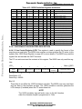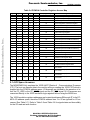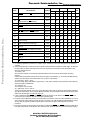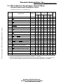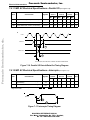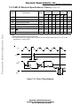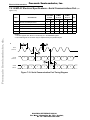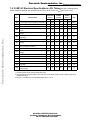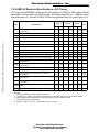
1
Freescale Semiconductor, Inc. Freescale Semiconductor, Inc... MC68PM302 Integrated Multiprotocol Processor with PCMCIA Reference Manual 1995 Motorola, Inc. All Rights Reserved For More Information On This Product, Go to: www.freescale.com Freescale Semiconductor, Inc. PREFACE The complete documentation package for the MC68PM302 consists of the MC68PM302RM/AD, MC68PM302 Low Power Integrated Multiprotocol Processor with PCMCIA Interface Reference Manual, M68000PM/AD, MC68000 Family Programmer’s Reference Manual, MC68302UM/AD, MC68302 Integrated Multiprotocol Processor User’s Manual, and the MC68PM302/D, MC68PM302 Low Power Integrated Multiprotocol Processor with PCMCIA Interface Product Brief. Freescale Semiconductor, Inc... The MC68PM302 Low Power Integrated Multiprotocol Processor with PCMCIA Interface Reference Manual describes the programming, capabilities, registers, and operation of the MC68PM302 that differ from the original MC68302; the MC68000 Family Programmer’s Reference Manual provides instruction details for the MC68PM302; and the MC68PM302 Low Power Integrated Multiprotocol Processor with PCMCIA Interface Product Brief provides a brief description of the MC68PM302 capabilities. The MC68302 Integrated Multiprotocol Processor User’s Manual User’s Manual is required, since the MC68PM302 Low Power Integrated Multiprotocol Processor with PCMCIA Interface Reference Manual only describes the new features of the MC68PM302. This user’s manual is organized as follows: Section 1 Section 2 Section 3 Section 4 Section 5 Section 6 Section 7 Section 8 Introduction Configuration, Clocking, Low Power Modes, and Internal Memory Map System Integration Block (SIB) Communications Processor (CP) PCMCIA Controller Signal Description Electrical Characteristics Mechanical Data And Ordering Information ELECTRONIC SUPPORT: The Technical Support BBS, known as AESOP (Application Engineering Support Through On-Line Productivity), can be reach by modem or the internet. AESOP provides commonly asked application questons, latest device errata, device specs, software code, and many other useful support functions. Modem: Call 1-800-843-3451 (outside US or Canada 512-891-3650) on a modem that runs at 14,400 bps or slower. Set your software to N/8/1/F emulating a vt100. Internet: This access is provided by telneting to pirs.aus.sps.mot.com [129.38.233.1] or through the World Wide Web at http://pirs.aus.sps.mot.com. — Sales Offices — For questions or comments pertaining to technical information, questions, and applications, please contact one of the following sales offices nearest you. iii MC68PM302 REFERENCE MANUAL For More Information On This Product, Go to: www.freescale.com Freescale Semiconductor, Inc. Freescale Semiconductor, Inc... UNITED STATES ALABAMA, Huntsville ARIZONA, Tempe CALIFORNIA, Agoura Hills CALIFORNIA, Los Angeles CALIFORNIA, Irvine CALIFORNIA, Rosevllle CALIFORNIA, San Diego CALIFORNIA, Sunnyvale COLORADO, Colorado Springs COLORADO, Denver CONNECTICUT, Wallingford FLORIDA, Maitland FLORIDA, Pompano Beach/ Fort Lauderdal FLORIDA, Clearwater GEORGlA, Atlanta IDAHO, Boise ILLINOIS, Chicago/Hoffman Estates INDlANA, Fort Wayne INDIANA, Indianapolis INDIANA, Kokomo IOWA, Cedar Rapids KANSAS, Kansas City/Mission MARYLAND, Columbia (305) 486-9776 (813) 538-7750 (404) 729-7100 (208) 323-9413 (708) 490-9500 (219) 436-5818 (317) 571-0400 (317) 457-6634 (319) 373-1328 (913) 451-8555 (410) 381-1570 CANADA BRITISH COLUMBIA, Vancouver ONTARIO, Toronto ONTARIO, Ottawa QUEBEC, Montreal (604) 293-7605 (416) 497-8181 (613) 226-3491 (514) 731-6881 INTERNATIONAL AUSTRALIA, Melbourne AUSTRALIA, Sydney BRAZIL, Sao Paulo CHINA, Beijing FINLAND, Helsinki Car Phone FRANCE, Paris/Vanves GERMANY, Langenhagen/ Hanover GERMANY, Munich GERMANY, Nuremberg GERMANY, Sindelfingen GERMANY,Wiesbaden HONG KONG, Kwai Fong Tai Po INDIA, Bangalore ISRAEL, Tel Aviv ITALY, Milan JAPAN, Aizu JAPAN, Atsugi JAPAN, Kumagaya JAPAN, Kyushu JAPAN, Mito JAPAN, Nagoya JAPAN, Osaka JAPAN, Sendai JAPAN, Tachikawa JAPAN, Tokyo JAPAN, Yokohama KOREA, Pusan KOREA, Seoul (205) 464-6800 (602) 897-5056 (818) 706-1929 (310) 417-8848 (714) 753-7360 (916) 922-7152 (619) 541-2163 (408) 749-0510 (719) 599-7497 (303) 337-3434 (203) 949-4100 (407) 628-2636 (61-3)887-0711 (61(2)906-3855 55(11)815-4200 86 505-2180 358-0-35161191 358(49)211501 33(1)40 955 900 49(511)789911 49 89 92103-0 49 911 64-3044 49 7031 69 910 49 611 761921 852-4808333 852-6668333 (91-812)627094 972(3)753-8222 39(2)82201 81(241)272231 81(0462)23-0761 81(0485)26-2600 81(092)771-4212 81(0292)26-2340 81(052)232-1621 81(06)305-1801 81(22)268-4333 81(0425)23-6700 81(03)3440-3311 81(045)472-2751 82(51)4635-035 82(2)554-5188 MASSACHUSETTS, Marborough MASSACHUSETTS, Woburn MICHIGAN, Detroit MINNESOTA, Minnetonka MISSOURI, St. Louis NEW JERSEY, Fairfield NEW YORK, Fairport NEW YORK, Hauppauge NEW YORK, Poughkeepsie/Fishkill NORTH CAROLINA, Raleigh OHIO, Cleveland OHIO, Columbus Worthington OHIO, Dayton OKLAHOMA, Tulsa OREGON, Portland PENNSYLVANIA, Colmar Philadelphia/Horsham TENNESSEE, Knoxville TEXAS, Austin TEXAS, Houston TEXAS, Plano VIRGINIA, Richmond WASHINGTON, Bellevue Seattle Access WISCONSIN, Milwaukee/Brookfield MALAYSIA, Penang MEXICO, Mexico City MEXICO, Guadalajara Marketing Customer Service NETHERLANDS, Best PUERTO RICO, San Juan SINGAPORE SPAIN, Madrid or SWEDEN, Solna SWITZERLAND, Geneva SWITZERLAND, Zurich TAlWAN, Taipei THAILAND, Bangkok UNITED KINGDOM, Aylesbury (508) 481-8100 (617) 932-9700 (313) 347-6800 (612) 932-1500 (314) 275-7380 (201) 808-2400 (716) 425-4000 (516) 361-7000 (914) 473-8102 (919) 870-4355 (216) 349-3100 (614) 431-8492 (513) 495-6800 (800) 544-9496 (503) 641-3681 (215) 997-1020 (215) 957-4100 (615) 690-5593 (512) 873-2000 (800) 343-2692 (214) 516-5100 (804) 285-2100 (206) 454-4160 (206) 622-9960 (414) 792-0122 60(4)374514 52(5)282-2864 52(36)21-8977 52(36)21-9023 52(36)669-9160 (31)49988 612 11 (809)793-2170 (65)2945438 34(1)457-8204 34(1)457-8254 46(8)734-8800 41(22)7991111 41(1)730 4074 886(2)717-7089 (66-2)254-4910 44(296)395-252 FULL LINE REPRESENTATIVES COLORADO, Grand Junction Cheryl Lee Whltely (303) 243-9658 KANSAS, Wichita Melinda Shores/Kelly Greiving (316) 838 0190 NEVADA, Reno Galena Technology Group (702) 746 0642 NEW MEXICO, Albuquerque S&S Technologies, lnc. (505) 298-7177 UTAH, Salt Lake City Utah Component Sales, Inc. (801) 561-5099 WASHINGTON, Spokane Doug Kenley (509) 924-2322 ARGENTINA, Buenos Aires Argonics, S.A. (541) 343-1787 HYBRID COMPONENTS RESELLERS Elmo Semiconductor (818) 768-7400 Minco Technology Labs Inc. (512) 834-2022 Semi Dice Inc. (310) 594-4631 MC68PM302 REFERENCE MANUAL For More Information On This Product, Go to: www.freescale.com Freescale Semiconductor, Inc. TABLE OF CONTENTS Freescale Semiconductor, Inc... Paragraph Number 1.1 1.2 1.3 1.4 Title Page Number Section 1 Introduction Block Diagram......................................................................................... 1-1 Features .................................................................................................. 1-1 PM302 Applications ................................................................................ 1-4 PM302 Differences from Other Devices.................................................. 1-4 Section 2 Configuration, Clocking, Low Power Modes, and Internal Memory Map 2.1 MC68PM302 and MC68302 Signal Differences ..................................... 2-1 2.2 IMP Configuration Control....................................................................... 2-2 2.2.1 Base Address Register (BAR)................................................................. 2-4 2.3 System Configuration Registers.............................................................. 2-4 2.4 Clock Generation and Low Power Control .............................................. 2-5 2.4.1 PLL and Oscillator Changes to IMP ........................................................ 2-5 2.4.1.1 Clock Control Register ............................................................................ 2-5 2.4.2 MC68PM302 System Clock Generation ................................................. 2-6 2.4.2.1 Default System Clock Generation ........................................................... 2-7 2.4.3 IMP System Clock Generation ................................................................ 2-8 2.4.3.1 System Clock Configuration.................................................................... 2-8 2.4.3.2 On-Chip Oscillator................................................................................... 2-8 2.4.3.3 Phase-Locked Loop (PLL) ...................................................................... 2-8 2.4.3.4 Frequency Multiplication ......................................................................... 2-8 2.4.3.4.1 Low Power PLL Clock Divider................................................................. 2-9 2.4.3.4.2 IMP PLL and Clock Control Register (IPLCR) ...................................... 2-10 2.4.3.5 IMP Internal Clock Signals .................................................................... 2-11 2.4.3.5.1 IMP System Clock................................................................................. 2-11 2.4.3.5.2 BRG Clock ............................................................................................ 2-11 2.4.3.5.3 PIT Clock............................................................................................... 2-12 2.4.3.6 IMP PLL Pins ........................................................................................ 2-12 2.4.3.6.1 VCCSYN ............................................................................................... 2-12 2.4.3.6.2 GNDSYN............................................................................................... 2-12 2.4.3.6.3 XFC ....................................................................................................... 2-12 2.4.3.6.4 MODCLK............................................................................................... 2-12 2.4.4 IMP Power Management....................................................................... 2-12 2.4.4.1 IMP Low Power Modes ......................................................................... 2-12 2.4.4.1.1 STOP Mode .......................................................................................... 2-13 2.4.4.1.2 DOZE Mode .......................................................................................... 2-13 2.4.4.1.3 STAND_BY Mode ................................................................................. 2-13 MC68PM302 REFERENCE MANUAL For More Information On This Product, Go to: www.freescale.com Table of Contents Freescale Semiconductor, Inc... Paragraph Number Freescale Semiconductor, Inc. Title Page Number 2.4.4.1.4 2.4.4.1.5 2.4.4.1.6 2.4.4.1.7 2.4.4.1.8 2.4.4.1.9 2.4.4.2 2.4.4.2.1 2.4.4.2.2 2.4.4.2.3 2.4.4.2.4 2.4.4.3 2.4.4.3.5 2.4.4.3.6 2.5 2.6 SLOW_GO Mode...................................................................................2-13 NORMAL Mode......................................................................................2-14 IMP Operation Mode Control Register (IOMCR) ...................................2-14 Low Power Drive Control Register (LPDCR) .........................................2-14 IMP Power Down Register (IPWRD) .....................................................2-15 Default Operation Modes, ......................................................................2-15 Low Power Support................................................................................2-15 Enter the SLOW_GO mode ...................................................................2-15 Entering the STOP/ DOZE/ STAND_BY Mode......................................2-15 IMP Wake-Up from Low Power STOP Modes .......................................2-17 IMP Wake-Up Control Register – IWUCR .............................................2-17 Fast Wake-Up ........................................................................................2-18 Ring Oscillator Control Register (RINGOCR) ........................................2-19 Ring Oscillator Event Register (RINGOEVR). .......................................2-20 MC68PM302 Dual Port RAM .................................................................2-20 Internal Registers Map...........................................................................2-23 3.1 3.1.1 3.1.2 3.1.3 3.1.4 3.1.5 3.2 3.2.1 3.2.2 3.3 3.4 3.4.1 3.4.1.1 3.4.1.2 3.4.1.3 3.4.1.4 3.4.1.5 3.4.1.6 3.4.2 3.5 3.5.1 3.5.1.1 3.5.2 3.5.2.1 3.5.2.2 3.5.2.3 Section 3 System Integration Block (SIB) System Control ........................................................................................3-1 System Control Register (SCR) ...............................................................3-2 System Status Bits...................................................................................3-3 System Control Bits .................................................................................3-4 Hardware Watchdog ................................................................................3-6 Freeze Control .........................................................................................3-6 Programmable Data Bus Size Switch ......................................................3-7 Enabling the Dynamic Bus Switch ...........................................................3-7 Basic Procedure:.....................................................................................3-7 Load Boot Code from an SCC .................................................................3-8 DMA Control ..........................................................................................3-11 68PM302 Differences ............................................................................3-11 Channel Mode Register (CMR)..............................................................3-11 Source Address Pointer Register (SAPR) .............................................3-13 Destination Address Pointer Register (DAPR).......................................3-13 Function Code Register (FCR) ..............................................................3-14 Byte Count Register (BCR)....................................................................3-14 Channel Status Register (CSR) .............................................................3-14 Interface Signals ....................................................................................3-14 Interrupt Controller .................................................................................3-15 Interrupt Controller Key Differences from the MC68302........................3-15 Interrupt Controller Overview .................................................................3-15 Interrupt Controller Programming Model................................................3-15 Global Interrupt Mode Register (GIMR) .................................................3-15 Interrupt Pending Register (IPR)............................................................3-16 Interrupt Mask Register (IMR)................................................................3-17 MC68PM302 REFERENCE MANUAL For More Information On This Product, Go to: www.freescale.com Freescale Semiconductor, Inc. Freescale Semiconductor, Inc... Paragraph Number Title Table of Contents Page Number 3.5.2.4 3.6 3.6.1 3.6.2 3.6.2.1 3.6.2.2 3.6.3 3.6.4 3.7 3.7.1 3.7.1.1 3.7.1.2 3.7.1.3 3.7.1.4 3.7.1.5 3.7.2 3.7.2.1 3.7.2.2 3.7.3 3.7.3.1 3.7.3.2 3.7.3.3 3.7.3.4 3.8 3.8.1 3.8.1.1 3.8.1.2 3.8.1.3 3.8.2 3.8.3 3.8.3.1 3.8.3.2 3.9 Interrupt In-Service Register (ISR) ........................................................ 3-17 Parallel I/O Ports ................................................................................... 3-17 Port A .................................................................................................... 3-17 Port B .................................................................................................... 3-18 PB7–PB0............................................................................................... 3-18 PB11–PB8............................................................................................. 3-19 Port D .................................................................................................... 3-19 Port Registers........................................................................................ 3-19 Timers ................................................................................................... 3-20 General Purpose Timers Programming Model...................................... 3-20 Timer Mode Register (TMR1, TMR2).................................................... 3-20 Timer Reference Registers (TRR1, TRR2) ........................................... 3-21 Timer Capture Registers (TCR1, TCR2) ............................................... 3-21 Timer Counter (TCN1, TCN2) ............................................................... 3-21 Timer Event Registers (TER1, TER2) ................................................... 3-21 Timer 3 - Software Watchdog Timer ..................................................... 3-22 Software Watchdog Reference Register (WRR) ................................... 3-22 Software Watchdog Counter (WCN) ..................................................... 3-22 Periodic Interrupt Timer (PIT)................................................................ 3-22 Overview ............................................................................................... 3-23 Periodic Timer Period Calculation ......................................................... 3-23 Using the Periodic Timer As a Real-Time Clock ................................... 3-24 Periodic Interrupt Timer Register (PITR)............................................... 3-24 External Chip-Select Signals and Wait-State Logic .............................. 3-25 Chip-Select Registers............................................................................ 3-26 Base Register (BR3–BR0) .................................................................... 3-26 Option Registers (OR3–OR0) ............................................................... 3-26 PCMCIA Protection Register (PPR) ...................................................... 3-27 Disable CPU Logic (M68000)................................................................ 3-28 Bus Arbitration Logic ............................................................................. 3-29 Internal Bus Arbitration.......................................................................... 3-29 External Bus Arbitration Using HALT .................................................... 3-30 Dynamic RAM Refresh Controller ......................................................... 3-30 4.1 4.2 4.2.1 4.3 4.3.1 4.3.1.1 4.3.2 4.3.3 4.3.4 4.3.5 Section 4 Communications Processor (CP) MC68PM302 Key Differences from the MC68302 .................................. 4-1 Serial Channels Physical Interface.......................................................... 4-2 Serial Interface Registers ........................................................................ 4-2 Serial Communication Controllers (SCCs) .............................................. 4-2 SCC Configuration Register (SCON) ...................................................... 4-2 Divide by 2 Input Blocks (New Feature) .................................................. 4-2 Baud Rate Generator Pins Register–BRGP............................................ 4-2 SCC Mode Register (SCM) ..................................................................... 4-3 SCC Data Synchronization Register (DSR) ............................................ 4-4 Buffer Descriptors Table.......................................................................... 4-4 MC68PM302 REFERENCE MANUAL For More Information On This Product, Go to: www.freescale.com Table of Contents Freescale Semiconductor, Inc... Paragraph Number 4.3.6 4.3.7 4.3.8 4.3.8.1 4.3.8.2 4.3.8.3 4.3.8.4 4.3.8.5 4.3.8.6 4.3.9 4.3.9.1 4.3.9.2 4.3.9.3 4.3.9.4 4.3.9.4.1 4.3.9.4.2 4.3.9.4.3 4.3.9.4.4 4.3.9.5 4.3.9.6 4.3.9.7 4.3.9.8 4.3.9.8.1 4.3.9.8.2 4.3.9.9 4.3.10 4.3.10.1 4.3.10.2 4.3.10.3 4.3.10.4 4.3.10.5 4.3.10.6 4.3.11 4.3.11.1 4.3.11.2 4.3.11.3 4.3.11.4 4.3.11.5 4.3.11.6 4.3.12 4.3.12.1 4.3.12.2 4.3.12.3 4.3.12.4 4.3.12.5 Freescale Semiconductor, Inc. Title Page Number SCC Parameter RAM Memory Map.........................................................4-5 Interrupt Mechanism ................................................................................4-5 UART Controller.......................................................................................4-6 UART Memory Map .................................................................................4-6 UART Mode Register...............................................................................4-6 UART Receive Buffer Descriptor (Rx BD) ...............................................4-6 UART Transmit Buffer Descriptor (Tx BD)...............................................4-7 UART Event Register...............................................................................4-7 UART MASK Register..............................................................................4-7 Autobaud Controller (New) ......................................................................4-7 Autobaud Channel Reception Process ....................................................4-8 Autobaud Channel Transmit Process ......................................................4-9 Autobaud Parameter RAM.....................................................................4-10 Autobaud Programming Model ..............................................................4-11 Preparing for the Autobaud Process......................................................4-11 Enter_Baud_Hunt Command.................................................................4-12 Autobaud Command Descriptor.............................................................4-12 Autobaud Lookup Table.........................................................................4-14 Lookup Table Example ..........................................................................4-15 Determining Character Length and Parity..............................................4-16 Autobaud Reception Error Handling Procedure.....................................4-16 Autobaud Transmission .........................................................................4-17 Automatic Echo......................................................................................4-17 Smart Echo ............................................................................................4-17 Reprogramming to UART Mode or Another Protocol ............................4-18 HDLC Controller.....................................................................................4-18 HDLC Memory Map ...............................................................................4-18 HDLC Mode Register.............................................................................4-19 HDLC Receive Buffer Descriptor (Rx BD) .............................................4-19 HDLC Transmit Buffer Descriptor (Tx BD).............................................4-19 HDLC Event Register.............................................................................4-20 HDLC Mask Register .............................................................................4-20 BISYNC Controller .................................................................................4-20 BISYNC Memory Map............................................................................4-20 BISYNC Mode Register .........................................................................4-20 BISYNC Receive Buffer Descriptor (Rx BD)..........................................4-21 BISYNC Transmit Buffer Descriptor (Tx BD) .........................................4-21 BISYNC Event Register .........................................................................4-21 BISYNC Mask Register..........................................................................4-21 Transparent Controller ...........................................................................4-21 Transparent Memory Map......................................................................4-21 Transparent Mode Register ...................................................................4-22 Transparent Receive Buffer Descriptor (RxBD).....................................4-22 Transparent Transmit Buffer Descriptor (Tx BD) ...................................4-23 Transparent Event Register ...................................................................4-23 MC68PM302 REFERENCE MANUAL For More Information On This Product, Go to: www.freescale.com Freescale Semiconductor, Inc. Freescale Semiconductor, Inc... Paragraph Number 4.3.12.6 4.4 4.4.1 4.4.2 4.4.2.1 4.4.3 4.4.4 4.4.4.1 4.4.4.1.1 4.4.4.1.2 4.4.4.1.3 4.4.4.1.4 4.4.4.1.5 4.4.4.1.6 4.4.4.1.7 4.4.4.1.8 4.4.4.1.9 4.4.4.1.10 4.4.4.1.11 4.4.4.1.12 4.4.5 4.4.5.1 4.4.5.2 4.4.5.3 4.4.5.4 4.4.5.4.1 4.4.5.4.2 4.4.5.5 4.4.5.5.1 4.4.5.6 4.4.5.6.1 4.4.5.7 4.4.5.8 4.4.5.9 4.4.5.9.1 4.4.5.9.2 4.4.5.10 4.4.5.11 4.4.5.12 4.4.5.13 4.4.5.14 4.5 4.5.1 4.5.2 4.6 Title Table of Contents Page Number Transparent Mask Register ................................................................... 4-23 16550 Emulation Controller (NEW feature)........................................... 4-23 16550 Emulation Controller Features.................................................... 4-23 16550 Emulation Controller Overview................................................... 4-24 16550 Emulation Controller FIFOs Overview........................................ 4-24 PC Accesses ......................................................................................... 4-24 PC Programmer Model.......................................................................... 4-26 16550 Emulation Registers Description ................................................ 4-27 Line Control Register (LCR) .................................................................. 4-27 Line Status Register (LSR) (Read Only) ............................................... 4-28 FIFO Control Register (FCR) (Write Only) ............................................ 4-29 Interrupt Identification Register (IIR) (Read Only) ................................. 4-30 Interrupt Enable Register (IER) ............................................................. 4-31 MODEM Control Register (MCR) .......................................................... 4-31 MODEM Status Register (MSR)............................................................ 4-33 Divisor Latch (LS) - DLL ........................................................................ 4-34 Divisor Latch (LM) - DLM ...................................................................... 4-34 Receive Buffer Register (RBR) ............................................................. 4-34 Transmit Holding Register (THR) .......................................................... 4-35 Scratchpad Register (SCR)................................................................... 4-35 68000 Programming Model ................................................................... 4-35 16550 Memory Map .............................................................................. 4-35 16550 Emulation Mode Register (EMR)................................................ 4-36 16550 Command Set ............................................................................ 4-38 16550 Transmit Commands .................................................................. 4-38 STOP TRANSMIT Command................................................................ 4-38 RESTART TRANSMIT Command......................................................... 4-39 16550 Receive Commands ................................................................... 4-39 ENTER HUNT MODE Command.......................................................... 4-39 16550 Control Characters (Receiver).................................................... 4-39 Transmission of Out-of-Sequence Characters (Transmitter) ................ 4-40 BREAK Support (Receiver) ................................................................... 4-41 Send Break (Transmitter) ...................................................................... 4-41 16550 Error Handling ............................................................................ 4-41 IDLE Sequence Receive ....................................................................... 4-41 BREAK Sequence ................................................................................. 4-42 16550 Rx Buffer Descriptor (Rx BD) ..................................................... 4-42 16550 Tx Buffer Descriptor (Tx BD) ...................................................... 4-43 16550 Event Register............................................................................ 4-45 16550 Mask Register ............................................................................ 4-47 16550 Status Register........................................................................... 4-47 Serial Communication Port (SCP)......................................................... 4-48 SCP Programming Model...................................................................... 4-49 SCP Transmit/Receive Buffer Descriptor .............................................. 4-49 Serial Management Controllers (SMCs)................................................ 4-49 MC68PM302 REFERENCE MANUAL For More Information On This Product, Go to: www.freescale.com Table of Contents Freescale Semiconductor, Inc... Paragraph Number Freescale Semiconductor, Inc. Title Page Number 4.6.1 4.6.2 4.6.2.1 4.6.2.2 4.6.2.3 4.6.2.4 SMC Programming Model......................................................................4-49 SMC Memory Structure and Buffers Descriptors...................................4-49 SMC1 Receive Buffer Descriptor ...........................................................4-49 SMC1 Transmit Buffer Descriptor ..........................................................4-50 SMC2 Receive Buffer Descriptor ...........................................................4-50 SMC2 Transmit Buffer Descriptor ..........................................................4-50 5.1 5.1.1 5.1.2 5.1.3 5.1.4 5.1.5 5.1.6 5.1.7 5.1.8 5.1.9 5.1.9.1 5.1.10 5.1.10.1 5.1.10.2 5.1.10.3 5.1.10.4 5.2 5.2.1 5.2.2 5.2.3 5.3 5.3.1 5.3.2 5.3.3 5.3.4 5.3.5 5.3.6 5.3.7 5.3.8 5.3.9 5.3.10 5.3.10.1 5.3.10.2 5.3.10.3 5.3.10.4 5.3.10.5 Section 5 PCMCIA Controller PCMCIA Controller Functional Overview.................................................5-2 Attribute Memory Accesses .....................................................................5-4 Configuration Registers ...........................................................................5-5 Card Information Structure.......................................................................5-6 I/O Space Accesses.................................................................................5-7 Common Memory and Direct Access Mode Accesses ............................5-8 Protecting Memory and Internal Space from PCMCIA Accesses ..........5-12 PCMCIA Controller Initialization.............................................................5-13 PCMCIA to 68000 Bus Access and Monitoring Options ........................5-13 PCMCIA Ring Indication ........................................................................5-15 Wake Up Using the PwrDwn Bit ............................................................5-16 Wake Up Options...................................................................................5-16 Wake Up on PCMCIA Access in STAND-BY Mode...............................5-17 Power Down and Wake Up Using the PwrDwn Bit ................................5-17 PCMCIA Host Interrupts ........................................................................5-17 The Ready Busy Signal (Rdy/Bsy).........................................................5-19 PCMCIA Pins .........................................................................................5-19 PCMCIA Pins Supported by the MC68PM302.......................................5-19 PCMCIA Pins Not Supported.................................................................5-19 Pullup Control Register (PUCR) ............................................................5-20 Programmer’s Model..............................................................................5-22 PCMCIA Controller Accesses ................................................................5-22 PCMCIA Mode Register(PCMR)............................................................5-22 PCMCIA Configuration Registers Write Event Register (PCRWER) .....5-26 PCMCIA Configuration Registers Write Mask Register (PCRWMR) .....5-27 PCMCIA Access Wake-Up Event Register(PCAWER)..........................5-27 PCMCIA Access Wake-up Mask Register(PCAWMR) ..........................5-28 PCMCIA Host (PC) Event Register(PCHER).........................................5-29 CIS Base Address Register(CISBAR) ...................................................5-29 Common Memory Space Base Address Register (CMBAR1,2) ............5-30 Card Configuration Registers.................................................................5-31 Configuration Option Register - COR ....................................................5-31 Card Configuration and Status Register (CCSR)...................................5-32 Pin Replacement Register Organization (PRR).....................................5-33 Socket and Copy Register (SCR) ..........................................................5-34 I/O Event Indication Register (IOEIR) ....................................................5-35 MC68PM302 REFERENCE MANUAL For More Information On This Product, Go to: www.freescale.com Freescale Semiconductor, Inc. Freescale Semiconductor, Inc... Paragraph Number 5.3.10.6 5.3.11 5.3.11.1 5.3.11.1.1 5.3.11.1.2 5.3.11.2 5.3.11.3 5.3.11.4 5.3.11.4.3 5.3.11.4.4 5.3.11.4.5 5.3.11.4.6 6.1 6.1.1 6.1.2 6.1.3 6.1.4 6.1.5 6.1.6 6.1.7 6.1.8 6.1.9 6.1.10 6.1.11 6.1.12 6.1.13 6.1.14 6.1.15 6.1.16 6.1.17 6.1.18 6.1.19 6.1.20 6.1.21 6.1.22 6.1.23 6.1.24 6.2 6.3 6.4 Title Table of Contents Page Number Reserved Registers............................................................................... 5-36 PCMCIA DMA Support.......................................................................... 5-36 PC DMA Operation Description............................................................. 5-36 Interrupt/Polling Mode: .......................................................................... 5-37 IDMA Mode: .......................................................................................... 5-37 Data Path and Swapping Issues: .......................................................... 5-37 Description of Pin Reassignment .......................................................... 5-38 Description of Registers for PC_DMA ................................................... 5-38 PCMCIA Access Wake-Up Event Register (PCAWER) ........................ 5-38 PCMCIA Access Wake-Up Mask Register (PCAWMR) ........................ 5-39 PCMCIA Mode Register (PCMR) (Additional Bits)................................ 5-39 PCMCIA DMA Data Register (PCDMAD) (Mapped at Address Base+$878)........................................................................................... 5-40 Section 6 Signal Description IMP Pins .................................................................................................. 6-1 Mode Pins ............................................................................................... 6-6 Clock Pins ............................................................................................... 6-8 System Control Pins................................................................................ 6-9 IMP Address Bus Pins (A23–A1) .......................................................... 6-11 IMP Data Bus Pins (D15—D0) .............................................................. 6-12 Bus Control Pins.................................................................................... 6-12 Interrupt Control or Bus Arbitration Pins................................................ 6-14 Chip-Select Pins.................................................................................... 6-15 No-Connect Pins ................................................................................... 6-16 PGA Package Pins................................................................................ 6-16 IMP Bus Interface Signal Summary ...................................................... 6-17 Physical Layer Serial Interface Pins...................................................... 6-18 Typical Serial Interface Pin Configurations ........................................... 6-18 NMSI1 or ISDN Interface Pins............................................................... 6-19 NMSI2 Port or Port A Pins or PCMCIA Data Bus.................................. 6-21 NMSI3 Port or Port A Pins or SCP Pins ................................................ 6-23 IDMA or Port A Pins or PCMCIA Pins ................................................... 6-24 IACK or PIO Port B Pins or PCMCIA .................................................... 6-25 Timer Pins ............................................................................................. 6-26 Parallel I/O Pins with Interrupt Capability .............................................. 6-27 PCMCIA or Port D Pins ......................................................................... 6-28 IMP Arbitration or PCMCIA Pins ........................................................... 6-29 IMP Bus Control or PCMCIA Pins ......................................................... 6-30 IMP Address and Function Codes or PCMCIA Data............................. 6-32 Summary of Pin Multiplexing................................................................. 6-32 Power and Ground Pins ........................................................................ 6-34 When to Use Pullup Resistors............................................................... 6-34 Section 7 MC68PM302 REFERENCE MANUAL For More Information On This Product, Go to: www.freescale.com Table of Contents Freescale Semiconductor, Inc... Paragraph Number Freescale Semiconductor, Inc. Title Page Number 7.6.11 7.6.12 7.6.13 7.6.14 7.6.15 7.6.16 7.6.17 7.6.18 7.6.19 Electrical Characteristics Maximum Ratings ....................................................................................7-1 Thermal Characteristics ...........................................................................7-1 Power Considerations..............................................................................7-2 Power Dissipation ....................................................................................7-2 Layout Practices ......................................................................................7-3 Power Dissipation Considerations. ..........................................................7-3 DC Electrical Characteristics ...................................................................7-4 DC Electrical Characteristics—NMSI1 in IDL Mode ................................7-5 IMP Characteristics..................................................................................7-6 IMP AC Electrical Specifications Control Timing .....................................7-6 AC Electrical Characteristics - IMP Phased Lock Loop (PLL) Characteristics .........................................................................................7-7 IMP DC Electrical Characteristics—NMSI1 in IDL Mode .........................7-7 AC Electrical Specifications—IMP Bus Master Cycles ............................7-8 IMP AC Electrical Specifications—DMA ................................................7-15 IMP AC Electrical Specifications—External Master Internal Asynchronous Read/Write Cycles ............................................7-18 IMP AC Electrical Specifications—External Master Internal Synchronous Read/Write Cycles ..............................................7-21 IMP AC Electrical Specifications—Internal Master Internal Read/Write Cycles ....................................................................7-25 IMP AC Electrical Specifications—Chip-Select Timing Internal Master .......................................................................................7-25 IMP AC Electrical Specifications—Chip-Select Timing External Master......................................................................................7-27 IMP AC Electrical Specifications—Parallel I/O ......................................7-28 IMP AC Electrical Specifications—Interrupts .........................................7-28 IMP AC Electrical Specifications—Timers .............................................7-29 IMP AC Electrical Specifications—Serial Communications Port............7-30 IMP AC Electrical Specifications—IDL Timing.......................................7-31 IMP AC Electrical Specifications—GCI Timing ......................................7-33 IMP AC Electrical Specifications—PCM Timing ....................................7-35 IMP AC Electrical Specifications—NMSI Timing ...................................7-37 AC Electrical Specifications—PCMCIA Interface...................................7-39 8.1 8.1.1 8.1.2 8.2 8.2.1 8.2.2 8.3 Section 8 Mechanical Data and Ordering Information Pin Assignments ......................................................................................8-1 Pin Grid Array (PGA) ...............................................................................8-1 Surface Mount (TQFP).............................................................................8-2 Package Dimensions ...............................................................................8-3 Pin Grid Array (PGA) ...............................................................................8-3 Surface Mount (TQFP).............................................................................8-5 Ordering Information ................................................................................8-6 7.1 7.2 7.3 7.4 7.4.1 7.4.2 7.4.3 7.5 7.6 7.6.1 7.6.2 7.6.3 7.6.4 7.6.5 7.6.6 7.6.7 7.6.8 7.6.9 7.6.10 MC68PM302 REFERENCE MANUAL For More Information On This Product, Go to: www.freescale.com Freescale Semiconductor, Inc. Freescale Semiconductor, Inc... SECTION 1 INTRODUCTION Motorola has developed a derivative version of the well-known MC68302 integrated multiprotocol processor (IMP) called the MC68PM302. The PM302 has two modes of operation. In the first mode, it functions as an enhanced MC68302 with a new static 68000 core, a new timer and low power modes, and additional parallel I/O pins. In the second mode, it functions as the same enhanced MC68302, but with PCMCIA and 16550 UART functionality instead of the additional parallel I/O pins. The PM302 is packaged in a low profile 144 TQFP that is suitable for use in Type II PCMCIA cards. The Personal Computer Memory Card International Association (PCMCIA) has implemented a set of specifications for small form-factor cards. These cards were previously specified by a version number of the spec to which they complied. After the specification 2.1, these cards were named “PC Cards.” The PCMCIA functionality on the PM302 is compliant with the specification approved in October 1994. In addition, the PM302 contains a parallel interface and register set identical to the 16550 UART used in IBM-compatible PCs. This functionality is available when the PCMCIA mode is enabled, and shares pins with the PCMCIA interface. The document fully describes all the differences between the PM302 and the regular 68302. Any feature not described in this document will operate as described in the MC68302 User’s Manual. In addition this document contains the full set of electrical descriptions for the PM302. 1.1 BLOCK DIAGRAM The block diagram is shown in Figure 1-1. 1.2 FEATURES The features of the PM302 are as follows. The items in bold face type show major differences from the MC68302, although a complete list of differences is given in section 1.4 on page 4. • On-Chip Static 68000 Core Supporting a 16- or 8-Bit M68000 Family-System • SIB Including: Independent Direct Memory Access (IDMA) Controller. Interrupt Controller with Two Modes of Operation Parallel Input/Output (I/O) Ports, some with Interrupt Capability On-Chip 1152-Byte Dual-Port RAM MC68PM302 REFERENCE MANUAL For More Information On This Product, Go to: www.freescale.com Freescale Semiconductor, Inc. Introduction LOW POWER CONTROL 1 GENERALPURPOSE DMA CHANNEL INTERRUPT CONTROLLER 20 ADDRESS 8/16 DATA PIT Freescale Semiconductor, Inc... RAM / ROM 68000 SYSTEM BUS STATIC M68000 CORE RISC CONTROLLER 3 TIMERS 4 CHIP SELECTS PIO 6 SDMA CHANNELS 1152 BYTES DUAL-PORT RAM PERIPHERAL BUS 3 SERIAL CHANNELS (SCCs) PCMCIA SLAVE INTERFACE & UART 16550 INTERFACE 11 ADDRESS 8/16 DATA SCP + 2 SMCs 68PM302 Figure 1-1. MC68PM302 Block Diagram Three Timers Including a Watchdog Timer New Periodic Interrupt Timer (PIT) Four Programmable Chip-Select Lines with Wait-State Generator Logic Programmable Address Mapping of the Dual-Port RAM and IMP Registers On-Chip Clock Generator with Output Signal Glueless Interface to EPROM, SRAM, Flash EPROM, and EEPROM Allows Boot in 8-Bit Mode, and Running Switch to 16-bit Mode Allows System Clock to be Generated from 32 kHz or 4 MHz Crystals in Addition to a Full Speed Clock Oscillator System Control: System Status and Control Logic Disable CPU Logic (Slave Mode Operation) Hardware Watchdog New Low-Power (Standby) Modes in µA Range With Wake-up From Two Pins or PIT Timer Freeze Control for Debugging DRAM Refresh Controller • CP Including: Main Controller (RISC Processor) MC68PM302 REFERENCE MANUAL For More Information On This Product, Go to: www.freescale.com Freescale Semiconductor, Inc. Introduction Three Independent Full-Duplex Serial Communications Controllers (SCCs) Supporting Various Protocols: High-Level/Synchronous Data Link Control (HDLC/SDLC) Universal Asynchronous Receiver Transmitter (UART) Binary Synchronous Communication (BISYNC) Transparent Modes Autobaud Support Instead of DDCMP and V.110 Boot from SCC Capability Six Serial DMA Channels for the Three SCCs Flexible Physical Interface Accessible by SCCs Including ISDN Support: Freescale Semiconductor, Inc... Motorola Interchip Digital Link (IDL) General Circuit Interface (GCI, Also Known as IOM1-2) Pulse Code Modulation (PCM) Highway Interface Nonmultiplexed Serial Interface (NMSI) Implementing Standard Modem Signals SCP for Synchronous Communication Two Serial Management Controllers (SMCs) To Support IDL and GCI Auxiliary Channels • PCMCIA Controller Supports Slave Interface Having 8 or 16-bit Data Pins Compatible with the PC Card Classic Specification Approved in October 1994 Support for Ring Detect and Other Indications Support for Power Down Modes and Automatic Wakeup on Host Access Card Information Structure (CIS) Size and Location In Memory Programmable Supports DMA Accesses as Defined by PCMCIA Supports Direct Access to Common Memory Space for High Speed Buffer Transfers Security Option to Prevent Host Accesses to Sensitive Address Ranges • 16550 Emulation Block Complete H/W and S/W Emulation of the 16550 UART DMA Supported for Transfer of 16550 Data Over 68K bus Speed of Data Transfer Can Be Matched to Traditional 16550 UART High Speed Data Transfer up to 2 Mbps Possible • Initial Offering Features 16.67 and 20 MHz Versions at 5V and 3.3V • 144 Pin Thin Quad Flat Pack (TQFP) Packaging 1.3 PM302 APPLICATIONS The PM302 excels in several applications areas. 1. IOM is a trademark of Siemens AG MC68PM302 REFERENCE MANUAL For More Information On This Product, Go to: www.freescale.com Introduction Freescale Semiconductor, Inc. Freescale Semiconductor, Inc... First, the PM302 excels in low power and portable applications. The inclusion of a static 68000 core coupled with the low power modes built into the device make it ideal for handheld, or other low power applications. The new 32 kHz or 4 MHz PLL option greatly reduces the total power budget of the designer’s board, and allows the PM302 to be an effective device in low power systems. The PM302 can then optionally generate a full frequency clock for use by the rest of the board. During low power modes, the new periodic interrupt timer (PIT) allows the device to be woken up at regular intervals. In addition, two pins allow the device to be woken up from low power modes. These features make the device useful as an upgrade to the existing 68302. Second, the performance, cost, and low power usage of the PM302 is an ideal processor to be used on PCMCIA cards. It will perform the controller functions of a V.34 fax/data modem in conjunction with a separate data pump. With its PCMCIA and ISDN functionality on-chip, it can be gluelessly connected to an S/T or U interface device to perform the functions of a ISDN terminal adaptor. It can be used as a MAC controller for IEEE 802.11 wireless LANs. It may also be used as a wireless WAN PCMCIA controller for CDPD, Ardis, Mobitex, or digital cellular data applications. 1.4 PM302 DIFFERENCES FROM OTHER DEVICES The PM302 can be considered as a superset of another derivative called the MC68LC302. The LC302 does not have the PCMCIA and 16550 features, and only contains 2 SCCs. The PM302 can also be considered to be a subset of the MC68356. The 356 adds a full 56002 DSP with memory and, in one of its versions, contains a full V.34 fax/data data pump running on the DSP. When the PM302 is operating in its PCMCIA mode, certain functions existing on the original 68302 are no longer available. The major differences are listed below. • External masters are not able to take the bus away from the PM302 except through a simple scheme using the HALT pin. This restriction does not apply to using the PM302 is in CPU disabled mode (slave mode), in which case BR, BG, and BGACK are all available. • Although the Independent DMA (IDMA) is still available, the external IDMA request pins (DACK, and DONE) have been eliminated. • The DDCMP and V.110 protocols have been removed. • Four address lines have been eliminated, giving a total of 20 address lines. However, the PM302 supports more than a 1 MB addressing range, since each of the four chip selects still decodes a 24-bit address. This allows a total of 4 MB to be addressed. • The UDS, LDS, and R/W pins are not available except in slave mode, where they replace the WEH, WEL, and OE pins. Instead, the new pins WEH, WEL, and OE have been defined for glueless interfacing to memory. • PA12 is now muxed with the MODCLK pin, which is associated with the 32 kHz or 4 MHz PLL. The MODCLK pin is sampled at reset, and then becomes the PA12 pin. • BCLR, RMC and BRG1 pins have been eliminated • New VCCsyn, GNDsyn, and XFC pins have been added in support of the on-chip PLL. MC68PM302 REFERENCE MANUAL For More Information On This Product, Go to: www.freescale.com Freescale Semiconductor, Inc. Introduction • For purposes of emulation support only, a special 180 PGA version is supported. This version adds back the FC2-0, IAC, FRZ, and AVEC pins. The FC2-0 pins allow bus cycles to be distinguished between program and data accesses, interrupt cycles, etc. The IAC, FRZ, and AVEC pins are provided so that emulation vendors can quickly retrofit their existing 68302 emulator designs to support the PM302. Freescale Semiconductor, Inc... When the PM302 is not used in its PCMCIA mode, most of the original 68302 pins are returned to the device. However, even though the 68302 is also offered in a 144 TQFP, it was not possible to make the PM302 exactly pin compatible with the original 68302. Thus, the PM302 should not be used as a drop-in replacement for the 68302 in a 144 TQFP. MC68PM302 REFERENCE MANUAL For More Information On This Product, Go to: www.freescale.com Freescale Semiconductor, Inc. Freescale Semiconductor, Inc... Introduction MC68PM302 REFERENCE MANUAL For More Information On This Product, Go to: www.freescale.com Freescale Semiconductor, Inc. Freescale Semiconductor, Inc... SECTION 2 CONFIGURATION, CLOCKING, LOW POWER MODES, AND INTERNAL MEMORY MAP The MC68PM302 integrates a high-speed M68000 processor with multiple communications peripherals. The provision of direct memory access (DMA) control and link layer management with the serial ports allows high throughput of data for communications-intensive applications, such as basic rate Integrated Services Digital Network (ISDN). The MC68PM302 can operate either in the full MC68000 mode with a 16-bit data bus or in the MC68008 mode with an 8-bit data bus by connecting the BUSW/PC_ABUF pin low during reset. NOTE The BUSW pin is static and is not intended to be used for dynamic bus sizing. Instead the BSW and BSWEN bits in the PPR register should be used to switch the bus width after reset. Refer to the MC68000UM/AD, M68000 8-/16-/32-Bit Microprocessors User's Manual, and the MC68302UM/AD, MC68302 Integrated Multiprotocol Processor User’s Manual, for complete details of the on-chip microprocessor including the programming model and instruction set summary. Throughout this manual, references may use the notation M68000, meaning all devices belonging to this family of microprocessors, or the notation MC68000, MC68008, meaning the specific microprocessor products. This section is intended to describe configuration of the MC68PM302 and the differences between thePM302 and the MC68000 and the MC68302.This section also includes tables that show the registers of the IMP portion of the MC68PM302. All of the registers are memory mapped into the 68000 space 2.1 MC68PM302 AND MC68302 SIGNAL DIFFERENCES When the PM302 is operating in its PCMCIA mode, certain functions existing on the original 68302 are no longer available. The major differences are listed below. • External masters are not able to take the bus away from the PM302 except through a simple scheme using the HALT pin. This restriction does not apply to using the PM302 is in CPU disabled mode (slave mode), in which case BR, BG, and BGACK are all available. • Although the Independent DMA (IDMA) is still available, the external IDMA pins (DACK and DONE) have been eliminated. MC68PM302 REFERENCE MANUAL For More Information On This Product, Go to: www.freescale.com Freescale Semiconductor, Configuration, Clocking, Low Power Modes, and Internal Memory Map Inc. • Four address lines have been eliminated, giving a total of 20 address lines. However, the PM302 supports more than a 1 MB addressing range, since each of the four chip selects still decodes a 24-bit address. This allows a total of 4 MB to be addressed. • The FC2-0 pins have been eliminated. In CPU disabled mode (slave mode), these signals are internally driven to a value of 5 (Supervisor Data function code). • The UDS, LDS, and R/W pins are not available except in slave mode, where they replace the WEH, WEL, and OE pins. The new pins WEH, WEL, and OE are available in enable CPU mode. Their functionalities have been defined for glueless interfacing to memory. • PA12 is now muxed with the MODCLK pin, which is associated with the 32 kHz or 4 MHz PLL. The MODCLK pin is sampled at reset, and then becomes the PA12 pin. Freescale Semiconductor, Inc... • New VCCsyn, GNDsyn, and XFC pins have been added in support of the on-chip PLL. • For purposes of emulation support only, a special 180 PGA version is supported. This version adds back the FC2-0, IAC, FRZ, and AVEC pins. • PA7 is sampled during reset to enable Boot from SCC. When the PM302 is not used in its PCMCIA mode, most of the original 68302 pins are returned to the device. However, even though the 68302 is also offered in a 144 TQFP, it was not possible to make the PM302 exactly pin compatible with the original 68302. Thus, the PM302 should not be used as a drop-in replacement for the 68302 in a 144 TQFP. 2.2 IMP CONFIGURATION CONTROL A number of reserved entries in the external M68000 exception vector table are used as addresses for internal system configuration registers. See Table 2-1, System Configuration Registers. The BAR entry contains the BAR described in this section. The SCR entry contains the SCR described in Section 3 System Integration Block (SIB). Figure 2-1 shows all the IMP on-chip addressable locations and how they are mapped into system memory. The on-chip peripherals, including those peripherals in both the communications processor (CP) and system integration block (SIB), require a 4K-byte block of address space. This 4Kbyte block location is determined by writing the intended base address to the BAR in supervisor data space (FC = 5). In slave mode the FC2-0 pins are internally driven by the MC68PM302 to supervisor data space. In enable CPU mode, the Status Register of the M68000 should be set to supervisor mode, in order to access the supervisor data space. After a total system reset, the on-chip peripheral base address is undefined, and it is not possible to access the on-chip peripherals at any address until BAR is written. The BAR and the SCR can always be accessed at their fixed addresses. NOTE The BAR and SCR registers are internally reset only when a total system reset occurs by the simultaneous assertion of RESET MC68PM302 REFERENCE MANUAL For More Information On This Product, Go to: www.freescale.com Freescale Semiconductor, Inc.and Internal Memory Map Configuration, Clocking, Low Power Modes, SYSTEM MEMORY MAP $0 EXCEPTION VECTOR TABLE IMP $0F0 PITR $0F2 BAR ENTRY $0F4 SCR ENTRY $0F7 WAKE-UP $0F8 IMP PLL 256 VECTOR ENTRIES $3FF BAR POINTS TO THE BASE $0FA IMP MODE CONTROL Freescale Semiconductor, Inc... $0FB IMP POWER DOWN 4K BLOCK BASE + $0 SYSTEM RAM (DUAL-PORT) $xxx000 = BASE 4K BLOCK BASE + $400 PARAMETER RAM (DUAL-PORT) BASE + $800 INTERNAL REGISTERS BASE + $FFF $FFFFFF Figure 2-1. IMP Configuration Control and HALT. The chip-select (CS) lines are not asserted on accesses to these locations. Thus, it is very helpful to use CS lines to select external ROM/RAM that overlaps the BAR and SCR register locations, since this prevents potential bus contention. NOTE In 8-bit system bus operation, IMP accesses are not possible until the low byte of the BAR is written. Since the MOVE.W instruction writes the high byte followed by the low byte, this instruction guarantees the entire word is written. Do not assign other devices on the system bus an address that falls within the address range of the peripherals defined by the BAR. If this happens, a BERR is generated to the core (if the address decode conflict enable (ADCE) bit is set) and the address decode conflict (ADC) bit in the SCR is set. MC68PM302 REFERENCE MANUAL For More Information On This Product, Go to: www.freescale.com Freescale Semiconductor, Configuration, Clocking, Low Power Modes, and Internal Memory Map Inc. 2.2.1 Base Address Register (BAR) The BAR is a 16-bit, memory-mapped, read-write register consisting of the high address bits, the compare function code bit, and the function code bits. Upon a total system reset, its value may be read as $BFFF, but its value is not valid until written by the user. The address of this register is fixed at $0F2 in supervisor data space. BAR cannot be accessed in user data space. 15 13 Freescale Semiconductor, Inc... FC2–FC0 12 CFC 11 0 23 22 21 20 BASEADDRESS 19 18 17 16 15 14 13 12 Bits 15–13—FC2–FC0 The FC2–FC0 field is contained in bits 15–13 of the BAR. These bits are used to set the address space of 4K-byte block of on-chip peripherals. The address compare logic uses these bits, dependent upon the CFC bit, to cause an address match within its address space. When the core is enabled, the function code bits will be driven by the core to indicate the type of cycle in process. In disable CPU mode, the FC pins are not present unless the PCMCIA is disabled (they are internally driven to 5). In this situation, the user does not have any control over how the FC signals are driven, and it is recommended that the user write these bits to zero and write the CFC bit to zero to disable the FC comparison. NOTE Do not assign this field to the M68000 core interrupt acknowledge space (FC2–FC0 = 7). CFC—Compare Function Code 0 = The FC bits in the BAR are ignored. Accesses to the IMP 4K-byte block occur without comparing the FC bits. 1 = The FC bits in the BAR are compared. The address space compare logic uses the FC bits to detect address matches. Bits 11–0—Base Address The high address field is contained in bit 11–0 of the BAR. These bits are used to set the starting address of the dual-port RAM. The address compare logic uses only the most significant bits to cause an address match within its block size. Even though A23-20 are signals are not available, they are driven internally by the core, or driven to zeroes in disable CPU mode or when HALT has been asserted by an external master. 2.3 SYSTEM CONFIGURATION REGISTERS Four entries in the M68000 exception vectors table (located in low RAM) are reserved for the addresses of system configuration registers (see Table 2-1). These registers have seven addresses within $0F0-$0FF. The MC68PM302 uses one of the IMP 32-bit reserved spaces for 3 registers added for the MC68PM302. These registers are used to control the MC68PM302 REFERENCE MANUAL For More Information On This Product, Go to: www.freescale.com Freescale Semiconductor, Inc.and Internal Memory Map Configuration, Clocking, Low Power Modes, PLL, clock generation and low power modes. See 2.4 Clock Generation and Low Power Control. Table 2-1. System Configuration Registers Freescale Semiconductor, Inc... Address $0F0 $0F2 $0F4 $0F7 $0F8 $0FA $0FB $0FC Name PITR BAR SCR IWUCR IPLCR IOMCR IPDR RES Width 16 16 24 8 16 8 8 32 Description Periodic Interrupt Timer Register Base Address Register System Control Register IMP Wake-Up Control Register IMP PLL Control Register IMP Operations Mode Control Register IMP Power Down Register Reserved Reset Value 0000 BFFF 0000 0F 00 00 00 2.4 CLOCK GENERATION AND LOW POWER CONTROL The MC68PM302 includes a clock circuit that consists of crystal oscillator drive circuit capable of driving either an external crystal or accepting an oscillator clock, a PLL clock synthesizer capable of multiplying a low frequency clock or crystal such as a 32-kHz watch crystal up to the maximum clock rate of each processor, and a low power divider which allows dynamic gear down and gear up of the system clock for each processor on the fly. • On-Chip Clock Synthesizers (with output system clocks) —Oscillator Drive Circuits and Pins —PLL Clock Synthesizer Circuits with Low Power Output Clock Divider Block. • Low Power Control Of IMP —Slow-Go Modes using PLL Clock Divider Blocks —Varied Low Power STOP Modes for Optimizing Wake-Up Time to Low Power Mode Power Consumption: Stand-By, Doze and STOP. 2.4.1 PLL and Oscillator Changes to IMP The oscillator that was on the MC68302 has been replaced by the new clock synthesizer described in this section. The registers related to the oscillator have been either removed or changed according to the description below. Several control bits are still available but have new locations. The low power modes on the MC68302 have changed completely and will be discussed later in 2.4.4.1 IMP Low Power Modes 2.4.1.1 CLOCK CONTROL REGISTER. The clock control register address $FA is not implemented on the MC68PM302. This register location has been reassigned to the IOMCR and ICKCR registers. The clock control register bits have been reassigned as follows: CLKO Drive Options (CLKOMOD1–2) These bits are now in the IMP clock control register (IPLCR) on the MC68PM302, see 2.4.3.4.2 IMP PLL and Clock Control Register (IPLCR). MC68PM302 REFERENCE MANUAL For More Information On This Product, Go to: www.freescale.com Freescale Semiconductor, Configuration, Clocking, Low Power Modes, and Internal Memory Map Inc. Three-State TCLK1 (TSTCLK1) This bit is now in the BRGP register on the MC68PM302, see section 4.3.2 Baud Rate Generator Pins Register–BRGP. Three-State RCLK1 (TSRCLK1) This bit is now in the BRGP register on the MC68PM302,see section 4.3.2 Baud Rate Generator Pins Register–BRGP. Disable BRG1 (DISBRG1) This bit has been removed since the BRG1 pin was removed. Freescale Semiconductor, Inc... 2.4.2 MC68PM302 System Clock Generation Figure 2-3, the MC68PM302 system clock schematic, shows the IMP clock synthesizer. The block includes an on-chip oscillator, a clock synthesizer, and a low-power divider, which allows a comprehensive set of options for generating the system clock. The choices offer many opportunities to save power and system cost, without sacrificing flexibility and control. In addition to performing frequency multiplication, the PLL block can also provide EXTAL to CLKO skew elimination, and dynamic low power divides of the output PLL system clock. Clock source and default settings are determined during the reset of the IMP. The MC68PM302 decodes the MODCLK and VCCSYN pins and the value of these pins determines the initial clocking for the part. Further changes to the clocking scheme can be made by software. After reset, the 68000 core can control the IMP clocking through the following registers: 1. IMP Operation Mode Control Register, IOMCR (2.4.4.1.6 IMP Operation Mode Control Register (IOMCR)). 2. IMP PLL and Clock Control Register, IPLCR (2.4.3.4 Frequency Multiplication). 3. IMP Interrupt Wake-Up Control Register, IWUCR (2.4.4.2.4 IMP Wake-Up Control Register – IWUCR). 4. Periodic Interrupt Timer Register, PITR (See Section 3 System Integration Block (SIB)). MC68PM302 REFERENCE MANUAL For More Information On This Product, Go to: www.freescale.com Freescale Semiconductor, Inc.and Internal Memory Map Configuration, Clocking, Low Power Modes, Fast Wake Up RINGO MULTIPLICATION FACTOR (MF11–MF0) EXTAL PIN DIVIDE FACTOR (DF3–DF0) CLKIN IMP OSC. IMP PLL XTAL PIN (0 – 25MHz) VCO OUT En MUX Freescale Semiconductor, Inc... MUX MUX CLK OUT IMP SYSTEM CLOCK BRG CLOCK DIVIDE BY 2 MUX PIT CLOCK Figure 2-2. MC68PM302 PLL Clock Generation Schematic 2.4.2.1 DEFAULT SYSTEM CLOCK GENERATION. During the assertion of hardware reset, the value of the MODCLK and VCCSYN input pins determine the initial PLL settings according to Table 2-2. After the deassertion of reset, these pins are ignored. The MODCLK and VCCSYN pins control the IMP clock selection at hardware reset. The IMP PLL can be enabled or disabled at reset only and the multiplication factor preset to support different industry standard crystals. After reset, the multiplication factor can be changed in the IPLCR register, and the IMP PLL divide factor can be set in the IOMCR register. NOTE The IMP input frequency ranges are limited to between 25 kHz and the maximum operating frequency, and the PLL output frequency range before the low power divider is limited to between 10 MHz and the maximum system clock frequency (25 MHz). Table 2-2. Default System Clock Generation CSelect 0 0 0 VCCSYN MODCLK 0X 10 11 Example IMP EXTAL Freq. 25 MHz 4.192 MHz 32.768 kHz IMP PLL Disabled Enabled Enabled IMP IMP System Clock MF+1 x 4 401 IMP EXTAL IMP EXTALx4 IMP EXTALx401 Note: By loading the IPLCR register the user can change the multiplication factor of the PLL after RESET. By loading the IOMCR register, the user can change the power saving divide factor of the IMP PLL. NOTE It is not possible to start the system with PLL disabled and then enable the PLL with software programming. MC68PM302 REFERENCE MANUAL For More Information On This Product, Go to: www.freescale.com Freescale Semiconductor, Configuration, Clocking, Low Power Modes, and Internal Memory Map Inc. 2.4.3 IMP System Clock Generation 2.4.3.1 SYSTEM CLOCK CONFIGURATION. The IMP has an on-chip oscillator and phased locked loop (Figure 2-2). These features provide flexible ways to save power and reduce system cost. The operation of the clock generation circuitry is determined by the following registers. The IMP Operation Mode Control Register, IOMCR in 2.4.4.1.6 IMP Operation Mode Control Register (IOMCR). The IMP PLL and Clock Control Register, IPLCR in 2.4.3.3 Phase-Locked Loop (PLL). Freescale Semiconductor, Inc... PIT CLOCK EXTAL PIN IMP OSC. IMP SYSTEM CLOCK (0 – 25 MHZ) CLKIN XTAL PIN BRG CLOCK DIVIDE BY 2 MUX Figure 2-3. IMP System Clocks Schematic - PLL disabled Figure 2-2 shows the IMP system clocks schematic with the IMP PLL enabled. Figure 2-3 shows the IMP system clocks schematic with the IMP PLL disabled. The clock generation features of the IMP are discussed in the following paragraphs. 2.4.3.2 ON-CHIP OSCILLATOR. A 32.768-kHz watch crystal provides an inexpensive reference, but the EXTAL reference crystal frequency can be any frequency from 25 kHz to 6.0 MHz. Additionally, the system clock frequency can be driven directly into the EXTAL pin. In this case, the EXTAL frequency should be the exact system frequency desired (0 to Maximum operating frequency), and the XTAL pin should be left floating. Figure 2-4 shows all the external connections required for the on-chip oscillator (as well as the PLL VCC and GND connections). 2.4.3.3 PHASE-LOCKED LOOP (PLL). The IMP PLL’s main function is frequency multiplication. The phase-locked loop takes the CLKIN frequency and outputs a high-frequency source used to derive the general system frequency of the IMP. The IMP PLL is comprised of a phase detector, loop filter, voltage-controlled oscillator (VCO), and multiplication block. 2.4.3.4 FREQUENCY MULTIPLICATION. The IMP PLL can multiply the CLKIN input frequency by any integer between 1 and 4096. The multiplication factor may be changed to the desired value by writing the MF11–MF0 bits in the IPLCR. When the IMP PLL multiplier is modified in software, the IMP PLL will lose lock, and the clocking of the IMP will stop until MC68PM302 REFERENCE MANUAL For More Information On This Product, Go to: www.freescale.com Freescale Semiconductor, Inc.and Internal Memory Map Configuration, Clocking, Low Power Modes, VCC ~390pf x MF 0.1µF 330K CRYSTAL 20pf 0.01µF 20pf 20M XTAL EXTAL XFC VCCSYN GNDSYN CRYSTAL OSCILLATOR VCC Freescale Semiconductor, Inc... ICLVCC CLOCK GENERATION ICLGND 0.1µF CLKO Figure 2-4. PLL External Components lock is regained (worst case is 2500 EXTAL clocks). If an alteration in the system clock rate is desired without losing IMP PLL lock, the value in the low-power clock divider can be to modified to lower the system clock rate dynamically. The low power clock divider bits are located in the IOMCR register. NOTE If IMP PLL is enabled, the multiplication value must be large enough to result in the VCO clock being greater than 10 MHz. 2.4.3.4.1 Low Power PLL Clock Divider. The output of the IMP VCO is sent to a low power divider block. The clock divider can divide the output frequency of the VCO before it generates the system clock. The clock for the baud rate generators (BRGs) bypasses this clock divider. The purpose of the clock divider is to allow the user to reduce and restore the operating frequency of the IMP without losing the IMP’s PLL lock. Using the clock divider, the user can still obtain full IMP operation, but at a slower frequency. The BRG is not affected by the low power divider circuitry so previous BRG divider settings will not have to be changed when the divide factors are changed. When the PLL low power divider bits (DF0–3) are programmed to a non-zero value, the IMP is in SLOW_GO mode. The selection and speed of the SLOW_GO mode may be changed at any time, with changes occurring immediately. MC68PM302 REFERENCE MANUAL For More Information On This Product, Go to: www.freescale.com Freescale Semiconductor, Configuration, Clocking, Low Power Modes, and Internal Memory Map Inc. NOTE The IMP low power clock divider is active only if the IMP PLL is active. The low-power divider block is controlled in the IOMCR. The default state of the low-power divider is to divide all clocks by 1. Freescale Semiconductor, Inc... If the low-power divider block is not used and the user is concerned that errant software could accidentally write the IOMCR, the user may set a write protection bit in IOMCR to prevent further writes to the register. 2.4.3.4.2 IMP PLL and Clock Control Register (IPLCR). IPLCR is a 16-bit read/write register used to control the IMP’s PLL, multiplication factor and CLKO drive strength. This register is mapped in the 68000 bus space at address $0F8. If the 68000 bus is set to 8 bits (BUSW grounded at reset), during 8-bit accesses, changes to the IPLCR will take effect in the IMP PLL after loading the high byte of IPLCR (the low byte is written first). The WP bit in IPLCR is used as a protect mechanism to prevent erroneous writing. When this bit is set further accesses to the IPLCR will be blocked. IMP PLL and Clock Control Register (IPLCR) 15 14 IPLWP 13 CLKOMOD0–1 $0F8 12 11 10 9 8 PEN MF11 MF10 MF9 MF8 RESET 0 0 0 VCCSYN 0 0 0 VCCSYN/ MODCLK 7 6 5 4 3 2 1 0 MF7 MF6 MF5 MF4 MF3 MF2 MF1 MF0 0 0 VCCSYN/ MODCLK 0 0 MODCLK MODCLK RESET VCCSYN/ MODCLK1 Read/Write MF 11–0—Multiplication Factor These bits define the multiplication factor that will be applied to the IMP PLL input frequency. The multiplication factor can be any integer from 1 to 4096. The system frequency is ((MF bits + 1) x EXTAL). The multiplication factor must be chosen to ensure that the resulting VCO output frequency will be in the range from 10 MHz to the maximum allowed clock input frequency (e.g. 20 MHz for a 20 MHz IMP). The value 000 results in a multiplier value of 1. The value $FFF results in a multiplier value of 4096. Any time a new value is written into the MF11–MF0 bits, the IMP PLL will lose the lock condition, and after a delay of 2500 EXTAL clocks, will relock. When the IMP PLL loses its lock condition, all the clocks that are generated by the IMP PLL are disabled. After hardware reset, the MF11–MF0 bits default to either 0, 3 or 400 ($190 hex) depending on the MODCLK and VCCSYN pins (giving a multiplication factor of 1, 4 or 401). If the multiplication factor is 401, then a standard 32.768 kHz crystal generates an initial general system clock of 13.14 MHz. If the multiplication factor is 4, then a standard 4.192 MHz MC68PM302 REFERENCE MANUAL For More Information On This Product, Go to: www.freescale.com Freescale Semiconductor, Inc.and Internal Memory Map Configuration, Clocking, Low Power Modes, crystal generates an initial general system clock of 16.768 MHz. The user would then write the MF bits or adjust the output frequency to the desired frequency. NOTE Freescale Semiconductor, Inc... Since the clock source for the periodic interrupt timer is CLKIN (see Figure 2-2), the PIT timer is not disturbed when the IMP PLL is in the process of acquiring lock. PEN—PLL Enable Bit The PEN bit indicates whether the IMP PLL is operating. This bit is written by the MC68PM302 based on the value of VCCSYN during reset. When the IMP PLL is disabled, the VCO is not operating in order to minimize power consumption. During hardware reset this bit is set if the VCCSYN pin specifies that the IMP PLL is enabled. The only way to clear PEN is to hold the VCCSYN pin low during a hardware reset. 0 = The IMP PLL is disabled. Clocks are derived directly from the EXTAL pin. 1 = The IMP PLL is enabled. Clocks are derived from the CLKOUT output of the PLL. CLKODM0–1—CLKO Drive Mode 0–1 These bits control the output buffer strength of the CLKO pin. Those bits can be dynamically changed without generating spikes on the CLKO pin. Disabling CLKO will save power and reduce noise. 00 = Clock Out Enabled, Full-Strength Output Buffer. 01 = Clock Out Enabled, 2/3-Strength Output Buffer 10 = Clock Out Enabled, 1/3-Strength Output Buffer 11 = Clock Out Disabled (CLKO is driven high by internal pullup) NOTE These IMP bits are in a different address location than in the MC68302, where they are located at address $FA (bits 15, 14). IPLWP—IMP PLL Control Write Protect Bit This bit prevents accidental writing into the IPLCR. After reset, this bit defaults to zero to enable writing. Setting this bit prevents further writing (excluding the first write that sets this bit). 2.4.3.5 IMP INTERNAL CLOCK SIGNALS. The following paragraphs describe the IMP internal clock signals. 2.4.3.5.1 IMP System Clock. The IMP system clock is supplied to all modules on the IMP (with the exception of the BRG clocks which are connected directly to the VCO output with the PLL enabled). The IMP can be programmed to operate with or without IMP PLL. If IMP PLL is active, the system clock will be driven by PLL clock divider output. If IMP PLL is not active, the system clock will be driven by the PLL input clock (CLKIN). 2.4.3.5.2 BRG Clock. The clock to the BRGs can be supplied from the IMP PLL input (CLKIN) when the IMP PLL is disabled, or from the IMP PLL VCO output (when the PLL is enabled). The BRG prescaler input clock may be optionally programmed to be divided by 2 MC68PM302 REFERENCE MANUAL For More Information On This Product, Go to: www.freescale.com Freescale Semiconductor, Configuration, Clocking, Low Power Modes, and Internal Memory Map Inc. to allow very low baud rates to be generated from the system clock by setting the BCD bit in the IOMCR. 2.4.3.5.3 PIT Clock. CLKIN is supplied to the periodic interrupt timer (PIT) submodule which allows the PIT clock to run independently of the system clock (refer to Figure 2-2 and Section 3 System Integration Block (SIB)). 2.4.3.6 IMP PLL PINS. The following pins are dedicated to the IMP PLL operation. Freescale Semiconductor, Inc... 2.4.3.6.1 VCCSYN. This pin is the VCC dedicated to the analog IMP PLL circuits. The voltage should be well regulated, and the pin should be provided with an extremely low-impedance path to the VCC power rail if the PLL is to be enabled. VCCSYN should be bypassed to GNDSYN by a 0.1-µF capacitor located as close as possible to the chip package. VCCSYN should be tied to ground if the PLL is to be disabled. 2.4.3.6.2 GNDSYN. This pin is the GND dedicated to the analog IMP PLL circuits. The pin should be provided with an extremely low-impedance path to ground. GDNSYN should be bypassed to VCCSYN by a 0.1 µF capacitor located as close as possible to the chip package. The user should also bypass GNDSYN to VCCSYN with a 0.01 µF capacitor as close as possible to the chip package. 2.4.3.6.3 XFC. This pin connects to the off-chip capacitor for the PLL filter. One terminal of the capacitor is connected to XFC; the other terminal is connected to IQVCC. 2.4.3.6.4 MODCLK. MODCLK specifies what the initial VCO frequency is after a hardware reset if VCCSYN is tied high. During the assertion of RESET, the value of the VCCSYN and MODCLK input pins causes the PEN bit and the MF11–0 bits of the IMP PLL and Clock Control Register (IPLCR) $0F8 to be appropriately written.VCCSYN and MODCLK also determines if the oscillator’s prescaler is used. After RESET is negated, the MODCLK pins is ignored and becomes PA12. Table 2-2 shows the combinations of VCCSYN and MODCLK pins with the corresponding default settings. 2.4.4 IMP Power Management The IMP portion of the MC68PM302 has several low power modes from which to choose. 2.4.4.1 IMP LOW POWER MODES. The MC68PM302 provides a number of low power modes for the IMP section. Each of the operation modes has different current consumption, wake-up time, and functionality characteristics. The state of the IMP’s 68000 data and address bus lines can be either driven high, low or high impedance during low power stop mode by programming the low power drive control register (LPDCR). NOTE For lowest current consumption, the SCCs and BRGs should be disabled before entering the low power modes. Current consumption for all operating modes is specified in Section 7 Electrical Characteristics. MC68PM302 REFERENCE MANUAL For More Information On This Product, Go to: www.freescale.com Freescale Semiconductor, Inc.and Internal Memory Map Configuration, Clocking, Low Power Modes, Freescale Semiconductor, Inc... Table 2-3. IMP Low Power Modes - IMP PLL Enabled Operation Mode Oscillator STOP Not Active Not active Not active DOZE Active Not active Not active STAND_BY Active SLOW_GO/ NORMAL Active Active (if enabled Active (if enabled) PLL Clock Not active Active Current IMP Consumption Method of Entry/ LPM bits Functionality (Approximate) 70000 osc. Stop instruction/ <0.1mA No clocks LPM1–0=11 2500 osc. Stop instruction/ About 500uA No clocks LPM1–0=10 2–5 system Stop instruction/ Partial (BRG About 5mA clock cycles LPM1–0=01 clock is active) Low, depends on Write to DF3–0 Full CLK freq. Wake_Up 2.4.4.1.1 STOP Mode. In STOP mode, all parts of IMP are inactive and the current consumption is less than 0.1mA. Both the crystal oscillator and the IMP PLL are shut down. Because both the oscillator and the PLL must start up, the wake-up time takes 70000 EXTAL clocks (for example, 70000 cycles of 32.768 kHz crystal will take about 2.2 seconds). The STOP mode is entered by executing the STOP instruction with the LPM0–1 bits in the IOMCR register set to 11. Refer to 2.4.4.2.2 Entering the STOP/ DOZE/ STAND_BY Mode for an example instruction sequence for use with the STOP instruction. 2.4.4.1.2 DOZE Mode. In DOZE mode, the oscillator is active in the IMP but the IMP PLL is shut down. The current consumption depends on the frequency of the external crystal but is on the order of 500 µa. In DOZE mode, the IMP is shut down. The wake-up time is 2500 cycles of the external crystal (for example, 2500 cycles of 32.768 kHz crystal will take about 80 milliseconds). Doze mode has faster wake-up time than the STOP mode, at the price of higher current consumption. The DOZE mode is entered by executing the STOP instruction with the LPM1–0 bits in the IOMCR register set to 10. Refer to 2.4.4.2.2 Entering the STOP/ DOZE/ STAND_BY Mode for an example instruction sequence for use with the STOP instruction. 2.4.4.1.3 STAND_BY Mode. In STAND_BY mode, the oscillator is active, and the IMP PLL, if enabled, is active but the IMP clock is not active and the IMP is shut down. Current consumption in STAND-BY mode is less than less than 5mA. The wake up time is a few IMP system clock cycles. The STAND_BY mode is entered by executing the STOP instruction with the LPM1–0 bits in the IOMCR register set to 01. Refer to 2.4.4.2.2 Entering the STOP/ DOZE/ STAND_BY Mode for an example instruction sequence for use with the STOP instruction. In STAND-BY mode, the PCMCIA interface is active and any access on the PCMCIA interface will cause the IMP to come out of STAND-BY mode. The STAND_BY mode is useful in applications which have time slots with no activity, and require a minimal wake-up time before IMP returns to NORMAL or SLOW-GO mode. 2.4.4.1.4 SLOW_GO Mode. In the SLOW-GO mode, the IMP is fully operational but the IMP PLL divider has been programmed with a value that is dividing the IMP PLL VCO output to the system clock in order to save power. The PLL output divider can only be used with MC68PM302 REFERENCE MANUAL For More Information On This Product, Go to: www.freescale.com Freescale Semiconductor, Configuration, Clocking, Low Power Modes, and Internal Memory Map Inc. the IMP PLL enabled. The divider value is programmed in the DF3–0 bits in the IOMCR. The clock may be divided by a power of 2 (20 – 215). No functionality is lost in SLOW-GO mode. 2.4.4.1.5 NORMAL Mode. In NORMAL mode the IMP part is fully operational and the system clock from the PLL is not being divided down. 2.4.4.1.6 IMP Operation Mode Control Register (IOMCR). IOMCR is a 8-bit read/ write register used to control the operation modes of the IMP. The WP bit in IOMCR is used as a protect mechanism to prevent erroneous writing of IOMCR. IOMCR $0FA Freescale Semiconductor, Inc... 7 IOMWP RESET: 0 6 DF3 5 DF2 4 DF1 3 DF0 2 BCD 1 LPM1 0 LPM0 0 0 0 0 0 0 0 Read/Write IOMWP—IMP Operation Mode Control Write Protect Bit This bit prevents accidental writing into the IOMCR. After reset, this bit defaults to zero to enable writing. Setting this bit prevents further writing (excluding the first write that sets this bit). DF 3–0—Divide Factor The Divide Factor Bits define the divide factor of the low power divider of the PLL. These bits specify a divide range between 20 and 215. Changing the value of these bits will not cause a loss of lock condition to the IMP PLL. BCD—BRG Clock Divide Control This bit controls whether the divide-by-two block shown in Figure 2-2 is enabled. 0 = The BRG clock is divided by 1. 1 = The BRG clock is divided by 2. LPM—Low Power Modes When the 68000 core executes the STOP instruction, the IMP will enter the specified mode. LPM1–0: 00 = 01 = 10 = 11 = Normal - the IMP PLL and clock oscillator will continue to operate normally. Stand_by Mode DOZE Mode Stop Mode 2.4.4.1.7 Low Power Drive Control Register (LPDCR). This register controls the state of the IMP’s 68000 address and data buses during the Standby, Doze, and Stop modes. By programming this register it is possible to minimize power consumption due to external pullups or pull downs, or floating inputs. MC68PM302 REFERENCE MANUAL For More Information On This Product, Go to: www.freescale.com Freescale Semiconductor, Inc.and Internal Memory Map Configuration, Clocking, Low Power Modes, LPDCR BAR+$82A 7 6 5 4 3 2 LPAL 1 LPDL 0 LPDEN RESET: 0 0 0 0 0 0 0 0 Read/Write LPDEN—Low Power Drive Enable 0 - The IMP 68000 data and address buses will be high impedance. 1 - The IMP 68000 data and address buses to be driven according to the LPDL bit. Freescale Semiconductor, Inc... LPDL—Low Power Drive Data Low 0 - The data bus will be driven high when the LPDEN bit is set. 1 - The data bus will be driven low when the LPDEN bit is set. LPAL—Low Power Drive Address Low 0 - The address bus will be driven high when the LPDEN bit is set. 1 - The address bus will be driven low when the LPDEN bit is set. NOTE In 8-bit, non-PCMCIA mode, A0 is also driven during low power. With the PGA package in non-PCMCIA mode, the FC2-FC0 pins are also driven during low power. With the TQFP package in non-PCMCIA mode, the PC_D1–PC_D7 pins are also driven during low power. 2.4.4.1.8 IMP Power Down Register (IPWRD). The IPWRD is a 8-bit read/ write register located at $0FB that is used to control the low power operation of the IMP. This register must be written with the same operand as the STOP instruction that follows. This tells the hardware what level of interrupt (and above) will stop the MC68PM302 from entering low power if it occurs while the clocks are being stopped. 2.4.4.1.9 Default Operation Modes. See 2.4.2.1 Default System Clock Generation. 2.4.4.2 LOW POWER SUPPORT. The following sections describe how to enter the various low power modes. 2.4.4.2.1 Enter the SLOW_GO mode. When the required IMP performance can be achieved with a lower clock rate, the user can reduce power consumption by dividing IMP PLL output clock that provides the IMP system clock. Switching between the NORMAL and SLOW_GO modes is achieved by changing the DF3–0 field in the IOMCR register to a nonzero value. The IMP PLL will not lose lock when the DF3–0 field in the IOMCR register is changed. 2.4.4.2.2 Entering the STOP/ DOZE/ STAND_BY Mode. Entering the STOP/ STAND_BY mode is achieved by the 68000 core executing the following code: nop move.b *+6(PC),$000000FB ;copy STOP operand high byte to addr 000000fb stop #$xxxx ;xxxx -> SR nop MC68PM302 REFERENCE MANUAL For More Information On This Product, Go to: www.freescale.com DOZE/ Freescale Semiconductor, Configuration, Clocking, Low Power Modes, and Internal Memory Map Inc. This code is position independent. The core must be in the supervisor state to execute the STOP instruction, therefore the write to $000000FB must be done in the supervisor state (function code 5, supervisor data). The core trace exception should be disabled, otherwise the low power control will not enter the STOP mode. To guarantee supervisor state and trace exceptions disabled, this code should be part of a TRAP routine. Upon entering the trap routine, examine the stacked status register. If it indicates the supervisor state, then execute this code to enter STOP mode. If not supervisor, do NOT execute this code (could perform some application-specific error): TRAP_x btst.b #5,(SP) beq.s NO_STOP ; supervisor? Freescale Semiconductor, Inc... nop ; flush execution, bus pipes move.b *+6(PC),$000000FB ;copy STOP operand high byte to addr 000000fb stop #$xxxx ; xxxx -> SR nop rte NO_STOP ... ; error routine? NOTE The RI/PB9, DTE/PB10 and PIT conditions will generate a level 4 interrupt. The PCMCIA will generate a level 1, 6, or 7 interrupt. The user should set the 68000 interrupt mask register to the appropriate level before executing this code. IMP’s low power control logic will: 1. Detect the write cycle. 2. Check if bit 5 = 1 (supervisor space) (if it is 0, the low power request will be ignored). 3. Sample the interrupt mask bits (bits 0–2). If during this process of stopping the clocks an interrupt of higher level than the mask is asserted to the core, this process will abort. 4. Wait for 16 clocks to guarantee the execution of the STOP command by the core. BG and BGACK will reset the 16-clock counter and it will restart its count. 5. Assert bus request signal to the core. 6. Wait for Bus Grant from the core 7. Force the IMP to the selected power-down mode, as defined in Table 2-3. If the IMP is in STAND_BY mode, any PCMCIA access will initiate a wake-up from STAND_BY mode (See All PCMCIA locations (registers, CIS memory, etc.) that can be accessed by the host may also be accessed by the 68000 core. Power Down Options). NOTE The RI (PB9), DTE (PB10) and periodic interrupt timer timeout interrupts conditions will generate level 4 interrupts. The PCM- MC68PM302 REFERENCE MANUAL For More Information On This Product, Go to: www.freescale.com Freescale Semiconductor, Inc.and Internal Memory Map Configuration, Clocking, Low Power Modes, CIA controller can be programmed to generate either level 1, 6, or 7 interrupts. The user should also set the 68000 interrupt mask in the status register (SR) to the appropriate level before executing the STOP command to ensure that the IMP will wake up to the desired events. 2.4.4.2.3 IMP Wake-Up from Low Power STOP Modes. The IMP can wake up from STOP/DOZE/STAND_BY mode to NORMAL/SLOW_GO mode in response to inputs from the following sources: 1. Asserting both RESET and HALT (hard reset) pins. Freescale Semiconductor, Inc... 2. Asserting (high to low transition) either RI (PB9) or DTE (PB10) pins (if these interrupts are enabled). 3. A timeout of the periodic interrupt timer (if the PIT interrupt is enabled). 4. Reset of the PwrDwn bit in the PCMCIA card configuration and status register when the PCMCIA controller is enabled. When one of these events occur (and the corresponding event bit is set), the IMP low power controller will asynchronously restart the IMP clocks. Then IMP low power control logic will release the 68000 bus and the IMP will return to normal operation. If one of the above wakeup events occurs during the execution of the STOP command, the low power control logic will abort the power down sequence and return to normal operation. NOTE The PB9, PB10, and periodic interrupt timer timeout interrupts conditions will generate level 4 interrupts.The user should also set the 68000 interrupt mask in the status register (SR) to the appropriate level before executing the STOP command to ensure that the IMP will wake up to the desired events. 2.4.4.2.4 IMP Wake-Up Control Register – IWUCR. The IWUCR contains control for the wake-up options. This register can be read and written by the 68000 core. IWUCR 7 0 RESET: 0 $0F7 6 PITE 5 PB10E 4 PB9Ev 3 0 2 PITEn 1 PB10En 0 PB9En 0 0 0 0 0 0 0 Read/Write PB9Ev—PB9 Event This bit will be set to one when there is a high to low transition on the PB9 pin. When PB9En is set and PB9Ev is set, the IMP will wake-up from the selected power down state, and a PB9 Interrupt will be generated. The IMP cannot enter the power-down mode if MC68PM302 REFERENCE MANUAL For More Information On This Product, Go to: www.freescale.com Freescale Semiconductor, Configuration, Clocking, Low Power Modes, and Internal Memory Map Inc. PB9Ev and PB9En are both set to one. PB9Ev is cleared by writing a one (writing a zero has no effect). In modem applications RI should be connected to the PB9 pin. Freescale Semiconductor, Inc... PB10Ev—PB10 Event This bit will be set to one when there is a high to low transition on the PB10 pin. When PB10En is set and PB10Ev is set, the IMP will wake-up from the selected power down state, and the PB10 Interrupt will be generated. The IMP cannot enter the power-down mode when PB10Ev and PB10En are both set to one. PB10Ev is cleared by writing a one (writing a zero has no effect). In modem applications the DTE TxD line may be connected to the PB10 pin. PITEv—PIT Event This bit will be set to one when there is a time-out on the periodic interrupt timer (PIT). When PITEn bit is set and a time-out occurs (PITEv is set), the IMP will wake-up from the selected power down, and a PIT Interrupt will be generated. The IMP cannot enter the power-down mode if PITEv and PITEn are both set to one. PITEv is cleared by writing a one (writing a zero has no effect). PB9En—PB9 Enable This bit, when set, enables the IMP to wake up from power down mode and generate an interrupt when the PB9 Event bit becomes set. PB10En—PB10 Enable This bit, when set, enables the IMP to wake up from power down mode and generate an interrupt when the PB10 Event bit becomes set. PITEn—PIT Enable This bit, when set, enables the IMP to wake up from power down mode and generate an interrupt when the PIT event bit becomes set, see 3.7.3 Periodic Interrupt Timer (PIT). 2.4.4.3 Fast Wake-Up In a system clocked with a 32-kHz oscillator, the wake-up recovery time from doze and stop modes may be too long for some applications. In order to shorten this time, an internal ring oscillator (called Ringo) can clock the chip (the term 'real clock' in the following discussion refers to the clock whose source is the external oscillator or crystal; the PLL can be either enabled or disabled). Two reasons for using the fast wake-up are: 1. To allow PC access to the IMP/system bus when there is no need to wake up the real clock (e.g. read status of 16550). In this case, only the internal oscillator is enabled for the duration of the access. The PLL and other clock logic are not awakened. 2. To allow PC accesses and other logic to operate in the time frame between the wakeup command and the actual real clock recovery (from the external crystal or oscillator). NOTE If the SCCs use the internal clock, or if they use external clock and the Ringo/external frequency ratio does not comply with the MC68PM302 REFERENCE MANUAL For More Information On This Product, Go to: www.freescale.com Freescale Semiconductor, Inc.and Internal Memory Map Configuration, Clocking, Low Power Modes, 1 / 2.5 maximum ration specification, then they cannot be enabled until the real clock has resumed operation. The criteria for enabling Ringo and waking up the CPU (by giving it an interrupt) are: — RINGOEN=1 and an unmasked event in the PCMCIA access wake-up event register (PCAWER) occurs. — RINGOEN=1 and an unmasked PITEv, PB10Ev, or PB9Ev event occurs (please refer to the IWUCR register) The internal ring oscillator is not enabled if the PLL is disabled. A system with the PLL disabled has to have an external oscillator connected in order to shorten the wake-up time. Freescale Semiconductor, Inc... There are two possible interrupts to the CPU from the Ringo logic: — Interrupt when Ringo is enabled; the CPU is always interrupted when Ringo starts oscillating (RINGOEN bit enables both ring oscillator and enables the interrupt to the CPU). Event bits for this interrupt are all wake-up events. — Maskable interrupt when the system clock switches to the real clock. The event bit for this interrupt is in the ring oscillator event register. The Ringo interrupts can be either at level 1, 6, or 7 according to RICR bits. If the CPU determines that the system needs the real clock, it programs the RECLMODE bits which enables the oscillator and PLL and interrupts if necessary; if it decides that the system can go back to sleep, it executes the normal power-down sequence which turns off Ringo. Upon switching to the real clock, the CPU can be interrupted by programming the RICR bits. (Note that Ringo is turned off either at the end of a power down sequence, or when the PLL has gained lock). If the RECLMODE bits are programmed to enable the PLL and the oscillator, the user is allowed to enter low power mode after the real clock has resumed. The chip will not operate correctly if the CPU enters the low power sequence while the PLL is waking up. Resetting of the RINGOEN bit is allowed only if the system is clocked by the real clock. The CLKO signal can be disabled by software if the user cannot operate the system at the Ringo frequency. 2.4.4.3.5 Ring Oscillator Control Register (RINGOCR) RINGOCR 7 BAR+$81A 6 5 4 3 2 RICR RESET: 0 0 0 0 1 0 RINGOEN 0 0 RECLMODE 0 0 Read/Write RINGOEN — Ring Oscillator Enable 0 = Ring oscillator is not used 1 = Ring oscillator is enabled MC68PM302 REFERENCE MANUAL For More Information On This Product, Go to: www.freescale.com Freescale Semiconductor, Configuration, Clocking, Low Power Modes, and Internal Memory Map Inc. RECLMODE — Real Clock Mode 00 = Do not enable the real clock 01 = Enable the real clock and switch the system clock from Ringo to the real clock once it is stable 10 = Enable the real clock and generate an interrupt to the CPU after the switch occurs 11 = Reserved RICR — Ring Oscillator Interrupt Control 00 = Connect Ringo Interrupts to 68k interrupt request level 1 01 = Connect Ringo Interrupts to 68k Interrupt request level 6 10 = Connect Ringo Interrupts to 68k interrupt request level 7 11 = Reserved Freescale Semiconductor, Inc... 2.4.4.3.6 Ring Oscillator Event Register (RINGOEVR). BAR+$81B RINGOEVR 7 6 5 4 RESERVED 3 2 1 0 RECLSEV RESET: 0 0 0 0 0 0 0 0 Read/Write RECLSEV — Real Clock Switch Event 0 = Event has not occurred 1 = Real clock is now the system clock (This bit is reset by writing 1) Bits 7-1 — Reserved 2.5 MC68PM302 DUAL PORT RAM The internal 1152-byte dual-port RAM has 576 bytes of system RAM (see Table 2-4) and 576 bytes of parameter RAM (see Table 2-5). Table 2-4. System RAM Address Base + 000 • • • Base + 23F Base +240 • • • Base + 3FF Width Block Description 576 Bytes RAM User Data Memory Reserved (Not Implemented) The parameter RAM contains the buffer descriptors for each of the three SCC channels, the 16550 channel or SCC2, the SCP, and the two SMC channels. The memory structures of the three SCC channels are identical. When any SCC, SCP, or SMC channel buffer descriptors or parameters are not used, their parameter RAM area can be used for additional memory. For detailed information about the use of the buffer descriptors and protocol parameters in a specific protocol, see Section 4 CP. Base + 67E contains the MC68PM302 revision number. MC68PM302 REFERENCE MANUAL For More Information On This Product, Go to: www.freescale.com Freescale Semiconductor, Inc.and Internal Memory Map Configuration, Clocking, Low Power Modes, Freescale Semiconductor, Inc... Table 2-5. Parameter RAM Address Base + 400 Base + 408 Base + 410 Base + 418 Base + 420 Base + 428 Base + 430 Base + 438 Base + 440 Base + 448 Base + 450 Base + 458 Base + 460 Base + 468 Base + 470 Base + 478 Base + 480 • • • Base + 4BF Base + 4C0 • • • Base + 4FF Base + 500 Base + 508 Base + 510 Base + 518 Base + 520 Base + 528 Base + 530 Base + 538 Base + 540 Base + 548 Base + 550 Base + 558 Base + 560 Base + 568 Base + 570 Base + 578 Base + 580 • • • Base + 5BF Base + 5C0 • • • Base + 5FF Base + 600 Base + 608 Base + 610 Base + 618 Base + 620 Base + 628 Base + 630 Base + 638 Base + 640 Base + 648 Base + 650 Base + 658 Base + 660 Base + 666 Base + 668 Base + 66A Base + 66C Base + 66E # Base + 67A Base + 67C Base + 67E # Width 4 Word 4 Word 4 Word 4 Word 4 Word 4 Word 4 Word 4 Word 4 Word 4 Word 4 Word 4 Word 4 Word 4 Word 4 Word 4 Word Block SCC1 SCC1 SCC1 SCC1 SCC1 SCC1 SCC1 SCC1 SCC1 SCC1 SCC1 SCC1 SCC1 SCC1 SCC1 SCC1 SCC1 Description Rx BD 0 Rx BD 1 Rx BD 2 Rx BD 3 Rx BD 4 Rx BD 5 Rx BD 6 Rx BD 7 Tx BD 0 Tx BD 1 Tx BD 2 Tx BD 3 Tx BD 4 Tx BD 5 Tx BD 6 Tx BD 7 Specific Protocol Parameters SCC1 Reserved (Not Implemented) 4 Word 4 Word 4 Word 4 Word 4 Word 4 Word 4 Word 4 Word 4 Word 4 Word 4 Word 4 Word 4 Word 4 Word 4 Word 4 Word SCC2, 16550 SCC2, 16550 SCC2, 16550 SCC2, 16550 SCC2, 16550 SCC2, 16550 SCC2, 16550 SCC2, 16550 SCC2, 16550 SCC2, 16550 SCC2, 16550 SCC2, 16550 SCC2, 16550 SCC2, 16550 SCC2, 16550 SCC2, 16550 SCC2 Rx BD 0 Rx BD 1 Rx BD 2 Rx BD 3 Rx BD 4 Rx BD 5 Rx BD 6 Rx BD 7 Tx BD 0 Tx BD 1 Tx BD 2 Tx BD 3 Tx BD 4 Tx BD 5 Tx BD 6/DRAM Refresh Tx BD 7/DRAM Refresh Specific Protocol Parameters SCC2 Reserved (Not Implemented) 4 Word 4 Word 4 Word 4 Word 4 Word 4 Word 4 Word 4 Word 4 Word 4 Word 4 Word 4 Word 3 Word Word Word Word Word 6 Word Word Word Word SCC3 SCC3 SCC3 SCC3 SCC3 SCC3 SCC3 SCC3 SCC3 SCC3 SCC3 SCC3 SMC SMC1 SMC1 SMC2 SMC2 SMC1–SMC2 SCP SCC1–SCC3 CP Rx BD 0 Rx BD 1 Rx BD 2 Rx BD 3 Rx BD 4 Rx BD 5 Rx BD 6 Rx BD 7 Tx BD 0 Tx BD 1 Tx BD 2 Tx BD 3 ## Reserved Rx BD Tx BD Rx BD Tx BD Internal Use Rx/Tx BD BERR Channel Number MC68PM302 Revision Number MC68PM302 REFERENCE MANUAL For More Information On This Product, Go to: www.freescale.com Freescale Semiconductor, Configuration, Clocking, Low Power Modes, and Internal Memory Map Inc. Table 2-5. Parameter RAM Base + 680 • • • Base + 6BF Base + 6C0 • • • Base + 7FF SCC3 Specific Protocol Parameters SCC3 Reserved (Not Implemented) Freescale Semiconductor, Inc... # Modified by the CP after a CP or system reset. ## Tx BD 4, 5, 6, and 7 are not initially available to SCC3. (4.3.5 Buffer Descriptors Table for information on how they may be regained.) In addition to the internal dual-port RAM, a number of internal registers support the functions of the various M68000 core peripherals. The internal registers (see Table 2-6) are memorymapped registers offset from the BAR pointer and are located on the internal M68000 bus. NOTE All undefined and reserved bits within registers and parameter RAM values written by the user in a given application should be written with zero to allow for future enhancements to the device. MC68PM302 REFERENCE MANUAL For More Information On This Product, Go to: www.freescale.com Freescale Semiconductor, Inc.and Internal Memory Map Configuration, Clocking, Low Power Modes, 2.6 INTERNAL REGISTERS MAP Table 2-6. Internal Registers Map Freescale Semiconductor, Inc... Address Base + 800 Base + 802 Base + 804 Base + 808 Base + 80C Base + 80E * Base + 80F Base + 810 Base + 811 Base + 812 # Base + 814 * Base + 816 Base + 818 * Base + 81A Base + 81B* Base + 81C Base + 81E # Base + 820 # Base + 822 # Base + 824 # Base + 826 # Base + 828 # Base + 82A Base + 82C Base + 82E Base + 830 # Base + 832 # Base + 834 # Base + 836 # Base + 838 # Base + 83A # Base + 83C # Base + 83E # Base + 840 Base + 842 Base + 844 Base + 846 Base + 848 Base + 849 * Base + 84A Base + 84C Base + 84E Base + 850 Base + 852 Base + 854 Base + 856 Base + 858 Name RES CMR SAPR DAPR BCR CSR RES FCR RES Width 16 16 32 32 16 8 8 8 8 Block IDMA IDMA IDMA IDMA IDMA IDMA IDMA IDMA IDMA GIMR IPR IMR ISR RINGOCR RINGOEVR RES PACNT PADDR PADAT PBCNT PBDDR PBDAT LPDCR PPR RES BR0 OR0 BR1 OR1 BR2 OR2 BR3 OR3 TMR1 TRR1 TCR1 TCN1 RES TER1 WRR WCN RES TMR2 TRR2 TCR2 TCN2 RES 16 16 16 16 8 8 16 16 16 16 16 16 16 8 8 16 16 16 16 16 16 16 16 16 16 16 16 16 8 8 16 16 16 16 16 16 16 8 Int Cont Int Cont Int Cont Int Cont Low Power Low Power Int Cont PIO PIO PIO PIO PIO PIO PIO CS CS CS0 CS0 CS1 CS1 CS2 CS2 CS3 CS3 Timer Timer Timer Timer Timer Timer WD WD Timer Timer Timer Timer Timer Timer Description Reserved Channel Mode Register Source Address Pointer Destination Address Pointer Byte Count Register Channel Status Register Reserved Function Code Register Reserved Global Interrupt Mode Register Interrupt Pending Register Interrupt Mask Register In-Service Register RINGO Control Register RINGO Event Register Reserved Port A Control Register Port A Data Direction Register Port A Data Register Port B Control Register Port B Data Direction Register Port B Data Register Low Power Drive Control Register PCMCIA protection register Reserved Base Register 0 Option Register 0 Base Register 1 Option Register 1 Base Register 2 Option Register 2 Base Register 3 Option Register 3 Timer Unit 1 Mode Register Timer Unit 1 Reference Register Timer Unit 1 Capture Register Timer Unit 1 Counter Reserved Timer Unit 1 Event Register Watchdog Reference Register Watchdog Counter Reserved Timer Unit 2 Mode Register Timer Unit 2 Reference Register Timer Unit 2 Capture Register Timer Unit 2 Counter Reserved MC68PM302 REFERENCE MANUAL For More Information On This Product, Go to: www.freescale.com Reset Value 0000 XXXX XXXX XXXX XXXX 00 XX 0000 0000 0000 0000 00 00 0000 0000 XXXX ## 0080 0000 XXXX ## 00 0000 C001 DFFD C000 DFFD C000 DFFD C000 DFFD 0000 FFFF 0000 0000 00 FFFF 0000 0000 FFFF 0000 0000 Freescale Semiconductor, Configuration, Clocking, Low Power Modes, and Internal Memory Map Inc. Table 2-6. Internal Registers Map Freescale Semiconductor, Inc... Address Base + 859 * Base + 85A Base + 85C Base + 85E Base + 860 Base + 861 Base + 86F Base + 870 Base + 871 Base + 872 Base + 873 Base + 874 Base + 875 Base + 876 Base + 877 Base + 878 Base + 87a Base + 87F Base + 880 Base + 882 Base + 884 Base + 886 Base + 888 * Base + 889 Base + 88A Base + 88B Base + 88C Base + 88D Base + 88E Base + 890 Base + 892 Base + 894 Base + 896 Base + 898 * Base + 899 Base + 89A Base + 89B Base + 89C Base + 89D Base + 89E Base + 8A0 Base + 8A2 Base + 8A4 Base + 8A6 Base + 8A8 * Name TER2 RES RES RES CR Width Block 8 Timer 16 Timer 16 Timer 16 Timer 8 CP Reserved COR CCSR PRR PSCR IOEIR RES1 RES2 RES3 PCDMAD 8 8 8 8 8 8 8 8 16 RES SCON1 SCM1 DSR1 SCCE1 RES SCCM1 RES SCCS1 RES RES RES SCON2 SCM2 16 16 16 16 8 8 8 8 8 8 16 16 16 16 DSR2 16 SCCE2, E550 RES SCCM2, M550 RES SCCS2, S550 RES RES RES SCON3 SCM3 DSR3 SCCE3 16 8 8 8 8 8 16 16 16 16 16 8 PC Cont PC Cont PC Cont PC Cont PC Cont PC Cont PC Cont PC Cont PC DMA Reserved SCC1 SCC1 SCC1 SCC1 SCC1 SCC1 SCC1 SCC1 SCC1 SCC1 SCC1 SCC2 SCC2 SCC2 SCC2 16550 SCC2 16550 SCC2 SCC2 16550 SCC2 SCC2 16550 SCC2 SCC2 SCC3 SCC3 SCC3 SCC3 SCC3 Description Timer Unit 2 Event Register Reserved Reserved Reserved Command Register Reset Value 00 00 Configuration Option Register 00 Card Configuration and Status Register 00 Pin Replacement Register 00 Socket and Copy Register XX I/O Event Indication register 00 Reserved1 00 Reserved2 00 Reserved3 00 PC DMA Data Register Reserved SCC1 Configuration Register SCC1 Mode Register SCC1 Data Sync. Register SCC1 Event Register Reserved SCC1 Mask Register Reserved SCC1 Status Register Reserved Reserved Reserved SCC2 Configuration Register SCC2 Mode Register SCC2 Data Sync. Register 0004 0000 7E7E 00 00 00 0004 0000 7E7E SCC2,16550 Emulation Event Register 0000 Reserved SCC2,16550 Emulation Mask Register 00 Reserved SCC2,16550 Emulation Status Regis- 0000 ter Reserved Reserved Reserved SCC3 Configuration Register SCC3 Mode Register SCC3 Data Sync. Register SCC3 Event Register MC68PM302 REFERENCE MANUAL For More Information On This Product, Go to: www.freescale.com 0004 0000 7E7E 00 Freescale Semiconductor, Inc.and Internal Memory Map Configuration, Clocking, Low Power Modes, Table 2-6. Internal Registers Map Freescale Semiconductor, Inc... Address Base + 8A9 Base + 8AA Base + 8AB Base + 8AC Base + 8AD Base + 8AE Name RES SCCM3 RES SCCS3 RES RES Width 8 8 8 8 8 16 Block SCC3 SCC3 SCC3 SCC3 SCC3 SCC3 Base + 8B0 SPMODE 16 SCM Base + 8B2 # Base + 8B4 # Base + 8B6 SIMASK SIMODE 16 16 PCMR 24 PCMCIA Base + 8C4 * PCRWER 8 PCMCIA Base + 8C5 * PCAWER 8 PCMCIA Base + 8C6 PCRWMR 8 PCMCIA Base + 8C7 PCAWMR 8 PCMCIA Base + 8C8 * Base + 8CC PCHER CISBAR 8 16 PCMCIA PCMCIA Base + 8D0 CMBAR1 16 PCMCIA Base + 8D4 CMBAR2 16 PCMCIA Base +8BF Base + 8C0 Base + 8D8 Base + 8DF Base + 8E0 Base + 8E2 Base + 8E4 Base + 8E6 Base + 8E8 Base + 8ED Base + 8EE Base + 8EF Base + 8F0 Base + 8F2 SI SI Reserved Description Reserved SCC3 Mask Register Reserved SCC3 Status Register Reserved Reserved SCP, SMC Mode and Clock Control Register Serial Interface Mask Register Serial Interface Mode Register Reset Value 00 00 0000 FFFF 0000 PCMCIA Mode Register 000000 PCMCIA Configuration Registers Write 00 Event Register PCMCIA Access Wake-up Event Reg- 00 ister PCMCIA Configuration Registers Write 00 Mask Register PCMCIA Access Wake-up Mask Regis- 00 ter PCMCIA Host (PC) Event Register 00 CIS Base Address Register 0000 Common Memory Space Base Ad0000 dress Register1 Common Memory Space Base Ad0000 dress Register2 Reserved PUCR RES RES PDDAT 8 16 16 16 Pull-Up Control Register Reserved Reserved Port D Data Register 00 XXXX* Baud Rate Generator Pins Register 0 Reserved BRGP 8 EMR LCR Reserve d 16 16550 8 16550 Base + 8F3 MSR 8 16550 Base + 8F4 Base + 8F5 Base + 8F6 Base + 8F7 DLM DLL LSR 8 8 8 16550 16550 16550 16550 Emulation Mode Register 0000 16550 Emulation Line Control Register 00 16550 Emulation Modem Status Regis- 00 ter 16550 Emulation Divisor Latch (MSB) XX 16550 Emulation Divisor Latch (LSB) XX 16550 Emulation Line Status Register 00 Reserved (Not implemented) Base + FFF # Reset only upon total system reset. (RESET and HALT assert together), but not on the execution of an M68000 RESET instruction. See the RESET pin description for details. ## The output latches are undefined at total system reset. * Event register with special properties. MC68PM302 REFERENCE MANUAL For More Information On This Product, Go to: www.freescale.com Inc. Freescale Semiconductor, Inc... Freescale Semiconductor, Configuration, Clocking, Low Power Modes, and Internal Memory Map MC68PM302 REFERENCE MANUAL For More Information On This Product, Go to: www.freescale.com Freescale Semiconductor, Inc. SECTION 3 SYSTEM INTEGRATION BLOCK (SIB) Freescale Semiconductor, Inc... The MC68PM302 contains an extensive SIB that simplifies the job of both the hardware and software designer. Most of the features are taken from the MC68302 without change, features that have been added or changed are highlighted in bold text. NOTE This section will only present the register descriptions for each block. For more information on the operation of each block, please refer to the MC68302 Users’ Manual. Items that are new or have changed will be described in detail. The SIB includes the following functions: • IDMA Controller with Three Handshake Signals: DREQ, DACK, and DONE • Interrupt Controller with Two Modes of Operation • More Parallel Input/Output (I/O) Ports, Some with Interrupt Capability • Pullup Resistors on Parallel Input and PCMCIA Input Pins • On-Chip 1152-Byte Dual-Port RAM • Four Timers Including a Watchdog Timer and Periodic Interrupt Timer • Four Programmable Chip-Select Lines with Wait-State Generator Logic • Glueless Interface to SRAM, EPROM, Flash EPROM, and EEPROM • System Control —System Status and Control Logic —Disable CPU Logic (M68000) —Bus Arbitration Logic with Low-Interrupt Latency Support —Hardware Watchdog for Monitoring Bus Activity —DRAM Refresh Controller —Programmable Bus Width • Boot from SCC 3.1 SYSTEM CONTROL The IMP system control consists of a System Control Register (SCR) that configures the following functions: • System Status and Control Logic MC68PM302 REFERENCE MANUAL For More Information On This Product, Go to: www.freescale.com Freescale System Integration Block (SIB) Semiconductor, Inc. • AS Control During Read-Modify-Write-Cycles • Disable CPU (M68000) Logic • Bus Arbitration Logic with Low-Interrupt Latency Support • Hardware Watchdog • Low-Power (Standby) Modes • Freeze Control Freescale Semiconductor, Inc... 3.1.1 System Control Register (SCR) The SCR is a 32-bit register that consists of system status and control bits, a bus arbiter control bit, and hardware watchdog control bits. Refer to Figure 3-1 and to the following paragraphs for a description of each bit in this register. The SCR is a memory-mapped read-write register. The address of this register is fixed at $0F4 in supervisor data space (FC = 5). MC68PM302 REFERENCE MANUAL For More Information On This Product, Go to: www.freescale.com Freescale Semiconductor, Inc. System Integration Block (SIB) $F4 31 30 29 28 27 26 25 24 EMEN 0 0 0 IPA HWT WPV ADC $F5 23 22 21 20 19 18 17 16 RME ERRE VGE WPVE RMCST EMWS ADCE BCLM $F6 15 14 13 12 11 FRZW FRZ2 FRZ1 SAM HWDEN 10 9 8 HWDCN2–HWDCN0 Freescale Semiconductor, Inc... Figure 3-1. System Control Register Table 3-1. SCR Register Bits Bit EMEN IPA HWT WPV ADC RME ERRE VGE WPVE RMCST EMWS ADCE BCLM FRZW FRZ1 FRZ2 SAM HWDEN HWDCN Name External Master Cycle Disabled Interrupt Priority Active Hardware Watchdog Timeout Write Protect Violation Address Decode Conflict Ram Microcode Enable External RISC Request Enable Vector Generation Enable Write Protect Violation Enable Read-Modify-Write Cycle Special Treatment External Master Wait State Address Decode Conflict Enable Bus Clear Mask Freeze Watch Dog Timer Enable Freeze Timer 1 Enable Freeze Timer 2 Enable Synchronous Access Mode Hardware Watchdog Enable Hardware Watchdog Count 3.1.2 System Status Bits Bits 27-24 of the SCR are used to report events recognized by the system control logic. On recognition of an event, this logic sets the corresponding bit in the SCR. The bits may be read at any time. A bit is reset by one and is left unchanged by zero. More than one bit may be reset at a time. For more information on these bits, please refer to the MC68302 Users’ Manual. MC68PM302 REFERENCE MANUAL For More Information On This Product, Go to: www.freescale.com Freescale System Integration Block (SIB) Semiconductor, Inc. IPA—Interrupt Priority Active This bit is set when the M68000 core has an unmasked interrupt request. NOTE If BCLM is set, an interrupt handler will normally clear IPA at the end of the interrupt routine to allow an alternate bus master to regain the bus; however, if BCLM is cleared, no additional action need be taken in the interrupt handler. Freescale Semiconductor, Inc... HWT—Hardware Watchdog Timeout This bit is set when the hardware watchdog (see 3.8.3 Bus Arbitration Logic) reaches the end of its time interval; BERR is generated following the watchdog timeout, even if this bit is already set. WPV—Write Protect Violation This bit is set when a bus master attempts to write to a location that has RW set to zero (read only) in its associated base register (BR3–BR0). ADC—Address Decode Conflict This bit is set when a conflict has occurred in the chip-select logic because two or more chip-select lines attempt assertion in the same bus cycle. 3.1.3 System Control Bits The system control logic uses seven control bits in the SCR. EMEN—External Master Cycle Using Halt Enable 0 = External master cycles using the HALT Arbitration are disabled. 1 = External master cycles using the HALT Arbitration are enabled. After system reset, this bit defaults to zero. This bit is used to enable the bus arbitration using HALT when the CPU is enabled and the PCMCIA interface is enabled. WPVE—Write Protect Violation Enable 0 = BERR is not asserted when a write protect violation occurs. 1 = BERR is asserted when a write protect violation occurs. RMCST—RMC Cycle Special Treatment 0 = The locked read-modify-write cycles of the TAS instruction will be identical to the M68000 (AS and CS will be asserted during the entire cycle). The arbiter will issue BG, regardless of the internal M68000 core RMC. If an IMP chip select is used, the DTACK generator will insert wait states on the read cycle only. 1 = The IMP uses the internal RMC to negate AS and CS at the end of the read portion of the RMC cycle and reasserts AS and CS at the beginning of the write portion. BG will not be asserted until the end of the write portion. If an IMP chip select is MC68PM302 REFERENCE MANUAL For More Information On This Product, Go to: www.freescale.com Freescale Semiconductor, Inc. System Integration Block (SIB) used, the DTACK generator will insert wait states on both the read and write portion of the cycles. Freescale Semiconductor, Inc... The assertion of the internal RMC by the M68000 core is seen by the arbiter and will prevent the arbiter from issuing bus grants until the completion of M68000-initiated locked read-modify-write activity. After system reset, this bit defaults to zero. EMWS—External Master Wait State (EMWS) (Valid only in Disable CPU Mode) When EMWS is set and an external master is using the chip-select logic for DTACK generation or is synchronously reading from the internal peripherals (SAM = 1), one additional wait state will be inserted in every memory cycle to external memory and peripherals and also in every cycle to internal memory and peripherals. When EMWS is cleared, all synchronous internal accesses will be with zero wait states, and the chip-select logic will generate DTACK after the exact programmed number of wait states. The chip-select lines are asserted slightly earlier for internal master memory cycles than for an external master. EMWS should be set whenever these timing differences will necessitate an additional wait state for external masters. After system reset, this bit defaults to zero. ADCE—Address Decode Conflict Enable 0 = BERR is not asserted by a conflict in the chip-select logic when two or more chipselect lines are programmed to overlap the same area. 1 = BERR is asserted by a conflict in the chip-select logic when two or more chip-select lines are programmed to overlap the same area. BCLM—Bus Clear Mask 0 = The arbiter does not use the M68000 core internal IPEND signal to assert the internal and external bus clear signals. 1 = The arbiter uses the M68000 core internal IPEND signal to assert the internal and external bus clear signals. SAM—Synchronous Access Mode (Valid only in Disable CPU Mode) This bit controls how external masters may access the IMP peripheral area. This bit is not relevant for applications that do not have external bus masters that access the IMP. In applications such as disable CPU mode, in which the M68000 core is not operating, the user should note that SAM may be changed by an external master on the first access of the IMP, but that first write access must be asynchronous with three wait states. (If DTACK is used to terminate bus cycles, this change need not influence hardware.) 0 = Asynchronous accesses. All accesses to the IMP internal RAM and registers (including BAR and SCR) by an external master are asynchronous to the IMP clock. Read and write accesses are with three wait states, and DTACK is asserted by the IMP assuming three wait-state accesses. This is the default value. 1 = Synchronous accesses. All accesses to the IMP internal RAM and registers (including BAR and SCR) must be synchronous to the IMP clock. Synchronous read accesses may occur with one wait state if EMWS is also set to one. MC68PM302 REFERENCE MANUAL For More Information On This Product, Go to: www.freescale.com Freescale System Integration Block (SIB) Semiconductor, Inc. RME—RAM Microcode Enable This bit is used to initiate the execution of Communication Processor microcode that has been loaded into the dual port RAM. 3.1.4 Hardware Watchdog The hardware watchdog logic is used to assert an internal BERR (BERR is driven externally wi the PCMCIA interface is disabled) and set HWT when a bus cycle is not terminated by DTACK and after a programmable number of clock cycles has elapsed. Freescale Semiconductor, Inc... The hardware watchdog logic uses four bits in the SCR. HWDEN—Hardware Watchdog Enable 0 = The hardware watchdog is disabled. 1 = The hardware watchdog is enabled. After system reset, this bit defaults to one to enable the hardware watchdog. HWDCN–HWDCN0—Hardware Watchdog Count 2–0 000 = BERR is asserted after 128 clock cycles (8 µs, 16-MHz clock) 001 = BERR is asserted after 256 clock cycles (16 µs, 16-MHz clock) 010 = BERR is asserted after 512 clock cycles (32 µs, 16-MHz clock) 011 = BERR is asserted after 1K clock cycles (64 µs, 16-MHz clock) 100 = BERR is asserted after 2K clock cycles (128 µs, 16-MHz clock) 101 = BERR is asserted after 4K clock cycles (256 µs, 16-MHz clock) 110 = BERR is asserted after 8K clock cycles (512 µs, 16-MHz clock) 111 = BERR is asserted after 16K clock cycles (1 ms, 16-MHz clock) After system reset, these bits default to all ones; thus, BERR will be asserted after 1 ms for a 16-MHz system clock. 3.1.5 Freeze Control Used to freeze the activity of selected peripherals, FRZ is useful for system debugging purposes. When FRZ is asserted (For more information on these bits, please refer to the MC68302 Users’ Manual): FRZ1 — Freeze Timer 1 Enable 0 = Freeze Timer 1 Logic is disabled 1 = Freeze Timer 1 Logic is enabled After system reset this bit defaults to zero. FRZ2 — Freeze Timer 2 Enable 0 = Freeze Timer 2Logic is disabled 1 = Freeze Timer 2Logic is enabled MC68PM302 REFERENCE MANUAL For More Information On This Product, Go to: www.freescale.com Freescale Semiconductor, Inc. System Integration Block (SIB) After system reset, this bit defaults to zero. FRZW — Freeze Watchdog Timer Enable 0 = Freeze Watchdog Timer Logic is disabled 1 = Freeze Watchdog Timer Logic is enabled After system reset this bit defaults to zero. 3.2 PROGRAMMABLE DATA BUS SIZE SWITCH The following procedure allows MC68PM302 to be booted in an 8 or 16 bit bus width and then switched to 16 or 8 bit bus width for future accesses. It does not implement true dynamic bus sizing, but allows a software reconfiguration of the BUSW pin. Freescale Semiconductor, Inc... 3.2.1 Enabling the Dynamic Bus Switch In order to enable the dynamic bus switch, the user must write the BSW bit in the PCMCIA Protection Register (See Section Section 3 System Integration Block (SIB)) and toggling the BSWEN bit in the PPR. 3.2.2 Basic Procedure: The MC68PM302 is booted in its 8-bit mode by externally connecting the BUSW pin to GND. It is expected that the MC68PM302 will be executing out of EPROM or Flash at this time, and that no external data memory is available in 8-bit mode. The MC68PM302 initializes the BAR register to place the 4K block of dual-port RAM and peripherals in an area that does not overlap the EPROM region. Note that this is part of a normal 302 initialization sequence. Also note that the CFC bit of the BAR register should NOT be set -- it must be cleared. At this time other desired initialization should be completed on the MC68PM302. No bus masters (IDMA, SDMA, or external) should be enabled. While in 8-bit mode, the MC68PM302 should initialize the external memory registers that control the16-bit external memory space. External memory refresh is not enabled at this time, but all other desired external memory control features should be enabled. Note that the MC68PM302 does not access the external memory itself yet, only the external memory control registers. The MC68PM302 now copies a special boot code to the user area of the internal dual-port RAM and then jumps to the start of that code. This code is copied as “data” to the dual-port RAM. To summarize, the procedure is then: • Boot up MC68PM302 • Perform required 8 bit operations • Write code to the Dual Port RAM for the bus width change • Jump to code in the dual port RAM MC68PM302 REFERENCE MANUAL For More Information On This Product, Go to: www.freescale.com Freescale System Integration Block (SIB) Semiconductor, Inc. • When ready to use 16 bit bus width, set the BUSW bit to 1 • Toggle the BWSEN bit from zero to one. • Allow time for bus arbitration and the instruction pipeline to clear • Initialize external memory • Copy boot code from EPROM to external memory space • Execute code from external memory space NOTE Freescale Semiconductor, Inc... The stack which is shared by both codes should be placed in the dual ported RAM. Copy the stack to dual port RAM after switching to the second RAM and change the stack pointer. 3.3 LOAD BOOT CODE FROM AN SCC The MC68PM302 provides the capability of downloading program code into SCC1 and beginning program execution in the dual port RAM. The boot function has two clocking options: external and internal. In the first mode, the user provides the chip with an external clock 16* the desired baud rate. In the second mode, the RISC processor programs the SCC into UART mode running at approximately 9600 baud (assuming the frequency of the clock to the chip has one of two nominal values 32.768 Khz or 4.192 Mhz). The first 576 bytes that are received into SCC1 are stored in the dual-port RAM. No error checking is performed on the incoming serial bit stream. The 68000 processor then begins executing from the first location of the dual-port RAM to complete the boot process. This function is not supported for SCC2 or SCC3. Three pins are sampled to determine the mode of operation and clock of the boot function: PA7–Sampled during Hard Reset (RESET and HALT asserted) 0 Boot from SCC is enabled 1 Boot from SCC is disabled PA5–Sampled within 100 clocks from the negation of RESET 0 Internal Clock 1 External Clock 16* the bit rate on TCLK1 and RCLK1 PA12 (MODCLK0) Sampled during Hard Reset (RESET and HALT asserted) 0 Nominal input frequency on EXTAL is 4.192 Mhz 1 Nominal input frequency on EXTAL is 32.768 Khz To enable the boot function, the PA7 pin must be pulled low during system reset. (System reset is defined by the RESET and HALT pins being asserted.) The PA7 pin must be pulled high during system reset, if boot mode is not to be enabled. Once the MC68PM302 detects that the PA7 pin is asserted, it internally keeps the HALT signal to the 68K core asserted MC68PM302 REFERENCE MANUAL For More Information On This Product, Go to: www.freescale.com Freescale Semiconductor, Inc. System Integration Block (SIB) after system reset is complete. This action prevents the 68000 from fetching the reset vector. NOTE PA7 needs to be either pulled UP or pulled DOWN. Do not leave this pin floating during reset. Once system reset is complete, the RISC processor programs the BAR register to $0000 to place the dual-port RAM at the low end of system memory. It then samples the PA5 pin to determine the clock source for the UART. Freescale Semiconductor, Inc... NOTE PA5 is expected to be valid for 100 clocks after the negation of RESET. If PA5 is pulled high, SCC1 is programmed for external clocks. In this mode, the user has to connect an external clock 16* the bit rate to TCLK1 and RCLK1. If PA5 is pulled low, the SCC is programmed for internal clocks and the TCLK1 and RCLK1 pins are programmed to three-state to avoid contention with user clocks. The RISC processor then programs the SCON register of the SCC based on PA12. The PA12 value sampled during reset (MODCLK0) is decoded in order to provide ~9600 bps with two input frequencies (4.192 Mhz and 32.768 Khz). • If MODCLK0 = GND, SCON1 is programmed to 0x00D8. • If MODCLK0 = VCC, SCON1 is programmed to 0x00A8. The following baud rates are achieved as a function of VCCSYN, MODCLK, and input clock: VCCSYN-MODCLK 00 20 Mhz 10 4.192 Mhz 10 4.8 Mhz 11 32.768 Khz 11467 bps (SCON1=0x00D8) 9614 bps (SCON1=0x00D8) 11009 bps (SCON1=0x00D8) 9662 bps (SCON1=0x00A8) The following paragraphs explain the boot process for the 32.768 Khz case in detail. If the clock provided to the MC68PM302 is 32.768 KHz, the system frequency is multiplied by 401 to get 13.139968 MHz. The CD10-CD0 bits of the SCON are programmed to 84 decimal giving a UART frequency of 9662. In summary, 13.139968 MHz / (84 + 1) / 16 = 9662. If the starting frequency is exactly 32.000 KHz, the UART frequency is 9435. NOTE The autobaud function cannot be used in the boot download process. Values in bit CD10:0 in SCON are not relevant if PA5=1 MC68PM302 REFERENCE MANUAL For More Information On This Product, Go to: www.freescale.com Freescale System Integration Block (SIB) Semiconductor, Inc. The RISC processor then programs the SCM register to $013D to program the SCC to UART mode with both the receiver and the transmitter enabled, software operation mode (CD and CTS are don't cares), 8-bit data characters, and no parity. The RISC processor then begins receiving data into the dual-port RAM beginning with location $0 of the dual-port RAM. Every character that is received is “echoed” back out of the TXD1 pin. The MC68PM302 UART must be sent 576 bytes of data from the external UART since the MC68PM302 will not leave the boot mode until 576 bytes are received. If the boot program is less than 576 bytes, the user is suggested to write $00 into the remaining locations. Freescale Semiconductor, Inc... After 576 bytes are received, the RISC programs the SCM register to $0, which clears the ENR and ENT bits to disable the UART (returns to its reset value). The RISC processor next negates the HALT signal to the core internally. The 68000 then reads the reset vector from the first location of the dual-port RAM. In most cases, the code that is downloaded will enable the chip selects of the MC68PM302, initialize the MC68PM302 receive buffer descriptors of SCC1 to continue receiving additional boot code into external system RAM, and re-initialize the UART receiver. NOTE The first 576 bytes also overlays the exception vector table, meaning that exception vectors will not work unless the user carefully maps the code around certain desired vectors and points those vectors into the 576 byte code space. In addition the stack pointer must point into the 576 bytes if any exceptions are to be taken within the boot code. All 68000 accesses to the dual port RAM are visible externally on the address and data pins so program execution in the 576 byte code space can be monitored. After the boot process is completed by the user, it is suggested that the user issue the CP Reset command to the CP command register (CR) before reinitializing the SCCs. This will return the CP to its original state and eliminate any possible inconsistencies in the initialization process. The RISC cannot return to boot mode unless a system reset is executed with the PA7 pin asserted low. Toggling of the PA7 pin when the device is not in system reset is allowed, and in this mode the PA7 pin can be used in its alternate functions. NOTE The user may wish to disable the software watchdog timer (Timer 3) in the initial boot code if a long delay (i.e. more than 10 seconds) can occur between the initial boot download and the rest of the download process. MC68PM302 REFERENCE MANUAL For More Information On This Product, Go to: www.freescale.com Freescale Semiconductor, Inc. System Integration Block (SIB) At the end of the Boot from SCC function, the following registers contain values that differ from their default reset values: ICR = 0xc000 BAR = 0x0000 SCON1 = depends on mode. The SCM1 register is reprogrammed to its reset value of 0x0 NOTE Freescale Semiconductor, Inc... During the boot from SCC procedure no external master should acquire the bus. 3.4 DMA CONTROL The IMP includes seven on-chip DMA channels, six serial DMA (SDMA) channels for the three serial communications controllers (SCCs) and one IDMA. 3.4.1 68PM302 Differences The DREQ, DACK, and DONE pins have been removed unless the PCMCIA interface is disabled. The user should not program the IDMA should for external request generation. If the PCMCIA interface is disabled, then the DREQ pin is available on PA13. If the PCMCIA Interface is enabled, then the DREQ pin is available on PB8 (see 6.2 Summary of Pin Multiplexing for more details on pin muxing). The external bus exceptions, BERR and retry, have been removed unless the PCMCIA interface is disabled. Only HALT or an internal BERR generated by the hardware watchdog timer or CS logic is supported. The rest of the functionality remains the same as for the MC68302. For details on the bus operation, please refer to the MC68302 User’s Manual. 3.4.1.1 Channel Mode Register (CMR). The CMR, a 16-bit register, is reset to $0000. 15 14 13 12 — ECO INTN INTE 11 10 REQG 9 8 SAPI DAPI 7 6 SSIZE 5 4 DSIZE 3 2 BT 1 RST 0 STR Bit 15—Reserved for future use. ECO—External Control Option (Only supported if the PCMCIA is disabled) 0 = If the request generation is programmed to be external in the REQG bits, the control signals (DACK and DONE) are used in the source (read) portion of the transfer since the peripheral is the source. 1 = If the request generation is programmed to be external in the REQG bits, the control signals (DACK and DONE) are used in the destination (write) portion of the transfer since the peripheral is the destination. MC68PM302 REFERENCE MANUAL For More Information On This Product, Go to: www.freescale.com Freescale System Integration Block (SIB) Semiconductor, Inc. INTN—Interrupt Normal 0 = When the channel has completed an operand transfer without error conditions as indicated by DONE, the channel does not generate an interrupt request to the IMP interrupt controller. The DONE bit remains set in the CSR. 1 = When the channel has completed an operand transfer without error conditions as indicated by DONE, the channel generates an interrupt request to the IMP interrupt controller and sets DONE in the CSR. NOTE Freescale Semiconductor, Inc... An interrupt will only be generated if the IDMA bit is set in the interrupt mask register (IMR). INTE—Interrupt Error 0 = If a bus error occurs during an operand transfer either on the source read (BES) or the destination write (BED), the channel does not generate an interrupt to the IMP interrupt controller. The appropriate bit remains set in the CSR. 1 = If a bus error occurs during an operand transfer either on BES or BED, the channel generates an interrupt to the IMP interrupt controller and sets the appropriate bit (BES or BED) in the CSR. NOTE An interrupt will only be generated if the IDMA bit is set in the IMR. REQG—Request Generation 00 = Internal request at limited rate (limited burst bandwidth) set by burst transfer (BT) bits 01 = Internal request at maximum rate (one burst) 10 = External request burst transfer mode-DREQ level sensitive 11 = External request cycle steal-DREQ edge sensitive NOTE The settings 10 and 11 will not work since the DREQ pin is not present. SAPI—Source Address Pointer (SAP) Increment 0 = SAP is not incremented after each transfer. 1 = SAP is incremented by one or two after each transfer, according to the source size (SSIZE) bits and the starting address. DAPI—Destination Address Pointer (DAP) Increment 0 = DAP is not incremented after each transfer. 1 = DAP is incremented by one or two after each transfer, according to the destination size (DSIZE) bits and the starting address. MC68PM302 REFERENCE MANUAL For More Information On This Product, Go to: www.freescale.com Freescale Semiconductor, Inc. System Integration Block (SIB) SSIZE—Source Size 00 = Reserved 01 = Byte 10 = Word 11 = Reserved Freescale Semiconductor, Inc... DSIZE—Destination Size 00 = Reserved 01 = Byte 10 = Word 11 = Reserved BT—Burst Transfer 00 = IDMA gets up to 75% of the bus bandwidth. 01 = IDMA gets up to 50% of the bus bandwidth. 10 = IDMA gets up to 25% of the bus bandwidth. 11 = IDMA gets up to 12.5% of the bus bandwidth. RST—Software Reset 0 = Normal operation 1 = The channel aborts any external pending or running bus cycles and terminates channel operation. Setting RST clears all bits in the CSR and CMR. STR—Start Operation 0 = Stop channel; clearing this bit will cause the IDMA to stop transferring data at the end of the current operand transfer. The IDMA internal state is not altered. 1 = Start channel; setting this bit will allow the IDMA to start (or continue if previously stopped) transferring data. NOTE STR is cleared automatically when the transfer is complete. 3.4.1.2 Source Address Pointer Register (SAPR) 31 24 23 0 RESERVED SOURCEADDRESSPOINTER The SAPR is a 32-bit register. Note that A23-A20 must be initialized by the user. They are driven internally by the IDMA and can be used by the chip selects for address comparison. 3.4.1.3 Destination Address Pointer Register (DAPR). The DAPR is a 32-bit register. 31 24 RESERVED 23 0 DESTINATIONADDRESSPOINTER Note that A23-A20 must be initialized by the user. They are driven internally by the IDMA and can be used by the chip selects for address comparison. MC68PM302 REFERENCE MANUAL For More Information On This Product, Go to: www.freescale.com Freescale System Integration Block (SIB) Semiconductor, Inc. 3.4.1.4 Function Code Register (FCR). The FCR is an 8-bit register. 7 6 1 4 DFC 3 2 1 0 SFC The function codes must e initialized by the user. The function code value programmed into the FCR is placed on pins FC2–FC0 during a bus cycle to further qualify the address bus value. NOTE Freescale Semiconductor, Inc... This register is undefined following power-on reset. The user should always initialize it and should not use the function code value “111” in this register. 3.4.1.5 Byte Count Register (BCR). This 16-bit register specifies the amount of data to be transferred by the IDMA; up to 64K bytes (BCR = 0) is permitted. 3.4.1.6 Channel Status Register (CSR). The CSR is an 8-bit register used to report events recognized by the IDMA controller. On recognition of an event, the IDMA sets its corresponding bit in the CSR (regardless of the INTE and INTN bits in the CMR). 7 4 RESERVED 3 2 1 0 DNS BES BED DONE Bits 7–4—These bits are reserved for future use. DNS—Done Not Synchronized (Only Valid if the PCMCIA is disabled) This bit is set if operand packing is performed between 16-bit memory and an 8-bit peripheral and the DONE signal is asserted as an input to the IDMA (i.e., by the peripheral) during the first access of the 8-bit peripheral. BES—Bus Error Source This bit indicates that the IDMA channel terminated with an error during the read cycle. BED—Bus Error Destination This bit indicates that the IDMA channel terminated with an error during the write cycle. DONE—Normal Channel Transfer Done This bit indicates that the IDMA channel has terminated normally. 3.4.2 Interface Signals When the PCMCIA interface is disabled, the IDMA channel has three dedicated control signals: DMA request (DREQ), DMA acknowledge (DACK), and end of IDMA transfer (DONE). The IDMA’s use of the bus arbitration signals is described in the MC68302 Users’ Manual. IDMA Operational Description MC68PM302 REFERENCE MANUAL For More Information On This Product, Go to: www.freescale.com Freescale Semiconductor, Inc. System Integration Block (SIB) NOTE For details on the IDMA programming and bus operation, please refer to Section 3 of the MC68302 Users’ Manual 3.5 INTERRUPT CONTROLLER The IMP interrupt controller accepts and prioritizes both internal and external interrupt requests and generates a vector number during the CPU interrupt acknowledge cycle. Freescale Semiconductor, Inc... 3.5.1 Interrupt Controller Key Differences from the MC68302 Since the function code pins are not connected externally unless the PCMCIA interface is disabled (or the PGA Package is used), the 68PM302 should be programmed to Dedicated Mode and to internally generate the vectors for Levels 1, 6, and 7. An external device will not easily be able to decode an IACK cycle and provide an vector back to the 68PM302. In Disable CPU mode with the PCMCIA interface enabled, the IRQ1, IRQ6, and IRQ7 become the BR, BGACK, and BG signals. With the core disabled, the MC68PM302 will not be able to decode an external CPU’s interrupt acknowledge cycle. The user must poll the Interrupt Pending Register (IPR) during interrupt handling to determine which peripheral caused the interrupt. If the PCMCIA interface is disabled, then the MC68PM302 can use the function codes to decode the interrupt acknowledge cycle and provide a vector back to the host CPU. 3.5.1.1 Interrupt Controller Overview. In addition to the MC68302 internal sources, the interrupt controller receives interrupts from the PCMCIA Controller and from the Fast WakeUp Ring Oscillator (see 2.4.4.3 Fast Wake-Up). These interrupts are additional sources to IRQ7, IRQ6, and IRQ1. (programmable in PCMR, DCOR and RINGOCR registers). With PCMCIA Interrupts it is possible to work in Normal or Dedicated mode for the three external interrupt requests pins. The chip ORs all sources at the same level and asserts the interrupt to the 68000 core. Interrupts at the same level (1,6 or 7) are not prioritized. 3.5.2 Interrupt Controller Programming Model The user communicates with the interrupt controller using four registers. The global interrupt mode register (GIMR) defines the interrupt controller's operational mode. The interrupt pending register (IPR) indicates which INRQ interrupt sources require interrupt service. The interrupt mask register (IMR) allows the user to prevent any of the INRQ interrupt sources from generating an interrupt request. The interrupt in-service register (ISR) provides a capability for nesting INRQ interrupt requests. 3.5.2.1 Global Interrupt Mode Register (GIMR). The user normally writes the GIMR soon after a total system reset. The GIMR is initially $0000 and is reset only upon a total system reset. 15 14 13 12 11 10 9 8 MOD IV7 IV6 IV1 — ET7 ET6 ET1 7 5 4 V7–V5 MC68PM302 REFERENCE MANUAL For More Information On This Product, Go to: www.freescale.com 0 RESERVED Freescale System Integration Block (SIB) Semiconductor, Inc. MOD—Mode 0 = Normal operational mode. Interrupt request lines are configured as IPL2–IPL0. 1 = Dedicated operational mode. Interrupt request lines are configured as IRQ7, IRQ6, and IRQ1. IV7—Level 7 Interrupt Vector 0 = Internal vector. 1 = External vector Freescale Semiconductor, Inc... IV6—Level 6 Interrupt Vector 0 = Internal vector. 1 = External vector. IV1—Level 1 Interrupt Vector 0 = Internal vector. 1 = External vector. ET7—IRQ7 Edge-/Level-Triggered 0 = Level-triggered. An interrupt is made pending when IRQ7 is low. 1 = Edge-triggered. An interrupt is made pending when IRQ7 changes from one to zero (falling edge). ET6—IRQ6 Edge-/Level-Triggered 0 = Level-triggered. An interrupt is made pending when IRQ6 is low. 1 = Edge-triggered. An interrupt is made pending when IRQ6 changes from one to zero (falling edge). ET1—IRQ1 Edge-/Level-Triggered 0 = Level-triggered. An interrupt is made pending when IRQ1 is low. 1 = Edge-triggered. An interrupt is made pending when IRQ1 changes from one to zero (falling edge). V7–V5—Interrupt Vector Bits 7–5 These three bits are concatenated with five bits provided by the interrupt controller, which indicate the specific interrupt source, to form an 8-bit interrupt vector number. If these bits are not written, the vector $0F is provided. NOTE: These three bits should be greater than or equal to ‘010’ in order to put the interrupt vector in the area of the exception vector table for user vectors. Bits 11 and 4–0—Reserved for future use. 3.5.2.2 Interrupt Pending Register (IPR). Each bit in the 16-bit IPR corresponds to an INRQ interrupt source. When an INRQ interrupt is received, the interrupt controller sets the corresponding bit in the IPR. MC68PM302 REFERENCE MANUAL For More Information On This Product, Go to: www.freescale.com Freescale Semiconductor, Inc. System Integration Block (SIB) 15 PB11 14 PB10 13 SCC1 12 SDMA 11 IDMA 10 SCC2 9 TIMER1 8 SCC3 7 PB9 6 TIMER2 5 SCP 4 TIMER3 3 SMC1 2 SMC2 1 PB8 0 ERR Freescale Semiconductor, Inc... 3.5.2.3 Interrupt Mask Register (IMR). Each bit in the 16-bit IMR corresponds to an INRQ interrupt source. The user masks an interrupt source by clearing the corresponding bit in the IMR. 15 PB11 14 PB10 13 SCC1 12 SDMA 11 IDMA 10 SCC2 9 TIMER1 8 SCC3 7 PB9 6 TIMER2 5 SCP 4 TIMER3 3 SMC1 2 SMC2 1 PB8 0 — 3.5.2.4 Interrupt In-Service Register (ISR) . Each bit in the 16-bit ISR corresponds to an INRQ interrupt source. In a vectored interrupt environment, the interrupt controller sets the ISR bit when the vector number corresponding to the INRQ interrupt source is passed to the core during an interrupt acknowledge cycle. The user's interrupt service routine should clear this bit during the servicing of the interrupt. 15 14 13 12 11 10 9 8 PB11 PB10 SCC1 SDMA IDMA SCC2 TIMER1 SCC3 7 6 5 4 3 2 1 0 PB9 TIMER2 SCP TIMER3 SMC1 SMC2 PB8 0 3.6 PARALLEL I/O PORTS The IMP supports three general-purpose I/O ports, port A, port B, and port D whose pins can be general-purpose I/O pins or dedicated peripheral interface pins. Some port B pins are always maintained as four general-purpose I/O pins, each with interrupt capability. 3.6.1 Port A Each of the 16 port A pins are independently configured as a general-purpose I/O pin if the corresponding port A control register (PACNT) bit is cleared. NOTE PA7-0 are only available if the PCMCIA interface is disabled or the PCMCIA data bus is only 8 bits wide. PA15-13 are only available when the PCMCIA interface is disabled. Port A pins are configured as dedicated on-chip peripheral pins if the corresponding PACNT bit is set. When acting as a general-purpose I/O pin, the signal direction for that pin is determined by the corresponding control bit in the port A data direction register (PADDR). (Note MC68PM302 REFERENCE MANUAL For More Information On This Product, Go to: www.freescale.com Freescale System Integration Block (SIB) Semiconductor, Inc. that these port pins do not have internal pullup resistors for non-PCMCIA mode). If a port A pin is selected as a general-purpose I/O pin, it may be accessed through the port A data register (PADAT). Freescale Semiconductor, Inc... Table 3-2. Port A Pin Functions PACNT Bit = 1 Pin Function RXD2 TXD2 RCLK2 TCLK2 CTS2 RTS2 CD2 SDS2/BRG2 RXD3 TXD3 RCLK3 TCLK3 BRG3 DREQ DACK PACNT Bit = 0 Pin Function PAO PA1 PA2 PA3 PA4 PA5 PA6 PA7 PA8 PA9 PA10 PA11 PA12 PA13 PA14 DONE PA15 Input to SCC2/SCC3/IDMA GND — GND RCLK2 # GND — GND — GND — GND RCLK3 # — GND — VDD # Allows a single external clock source on the RCLK pin to clock both the SCC receiver and transmitter. 3.6.2 Port B Port B has 12 pins. PB7–PB0 may be configured as general-purpose I/O pins or as dedicated peripheral interface pins; whereas, PB11–PB8 are always maintained as four generalpurpose pins, each with interrupt capability. NOTE PB2-0, and PB4 are only available when the PCMCIA interface is disabled. 3.6.2.1 PB7–PB0. Each port B pin may be configured as a general-purpose I/O pin or as a dedicated peripheral interface pin. PB7–PB0 functions exactly like PA15–PA0, except that PB7–PB0 is controlled by the port B control register (PBCNT), the port B data direction register (PBDDR), and the port B data register (PBDAT), and PB7 is configured as an opendrain output (WDOG) upon total system reset. Table 3-3 shows the dedicated function of each pin. The third column shows the input to the peripheral when the pin is used as a general-purpose I/O pin. MC68PM302 REFERENCE MANUAL For More Information On This Product, Go to: www.freescale.com Freescale Semiconductor, Inc. System Integration Block (SIB) Freescale Semiconductor, Inc... Table 3-3. Port B Pin Functions PBCNT Bit = 1 Pin Function PBCNT Bit = 0 Pin Function Input to Interrupt Control and Timers IACK7 PB0 — IACK6 PB1 — IACK1 PB2 — TIN1 PB3 GND TOUT1 PB4 — TIN2 PB5 GND TOUT2 PB6 — WDOG PB7 — 3.6.2.2 PB11–PB8. PB11–PB8 are four general-purpose I/O pins continuously available as general-purpose I/O pins and, therefore, are not referenced in the PBCNT. PB8 operates like PB11–PB9 except that it can also be used as the DRAM refresh controller request pin, as selected in the system control register (SCR). NOTE If the PIT is enabled, then the PB8 pin will not generate an interrupt, since the PIT uses the PB8 interrupt in the IPR, IMR, and ISR. 3.6.3 Port D When the PCMCIA interface is disabled (PC_EN tied to GND), 7 general purpose INPUT ONLY pins are available as port D.These pins also have optional internal pull-up resistors (see Pullup Control Register (PUCR) on page 20). Port D may be accessed through the Port D data register (PDDAT). When PDDAT is read, the state of the input pins is read. 3.6.4 Port Registers The I/O port consists of three memory-mapped read-write 16-bit registers for port A and three memory-mapped read-write 16-bit registers for port B. Refer to Figure 3-2 for the I/O port registers. The reserved bits are read as zeros. Port A Control Register (PACNT) 15 14 13 12 11 10 9 8 7 6 5 4 3 2 1 0 CA CA CA CA CA CA CA CA CA CA CA CA CA CA CA CA 0 = I/O 1 = Peripheral Port A Data Direction Register (PADDR) 15 14 13 12 11 10 9 8 7 6 5 4 3 2 1 0 DA DA DA DA DA DA DA DA DA DA DA DA DA DA DA DA 0 = Input 1 = Output MC68PM302 REFERENCE MANUAL For More Information On This Product, Go to: www.freescale.com Freescale System Integration Block (SIB) Semiconductor, Inc. Port A Data Register (PADAT) 15 14 13 12 11 10 9 8 7 6 5 4 3 2 1 0 PA PA PA PA PA PA PA PA PA PA PA PA PA PA PA PA Port B Control Register (PBCNT) 15 8 RESERVED 0 = I/O 7 6 5 4 3 2 1 0 CB CB CB CB CB CB CB CB 1 = Peripheral Port B Data Direction Register (PBDDR) 15 12 Freescale Semiconductor, Inc... RESERVED 0 = Input 11 10 9 8 7 6 5 4 3 2 1 0 DB DB DB DB DB DB DB DB DB DB DB DB 11 10 9 8 7 6 5 4 3 2 1 0 PB PB PB PB PB PB PB PB PB PB PB PB 1 = Output Port B Data Register (PBDAT) 15 12 RESERVED Port D Data Register (PDDAT) 15 14 13 12 11 10 9 8 7 6 5 4 3 2 1 0 0 PD PD PD PD PD PD PD 0 0 0 0 0 0 0 0 Figure 3-2. Parallel I/O Port Registers 3.7 TIMERS The MC68PM302 includes four timer units: two identical general-purpose timers, a software watchdog timer, and a periodic interrupt timer (PIT). Each general-purpose timer consists of a timer mode register (TMR), a timer capture register (TCR), a timer counter (TCN), a timer reference register (TRR), and a timer event register (TER). The TMR contains the prescaler value programmed by the user. The software watchdog timer, which has a watchdog reference register (WRR) and a watchdog counter (WCN), uses a fixed prescaler value. 3.7.1 General Purpose Timers Programming Model 3.7.1.1 Timer Mode Register (TMR1, TMR2). TMR1 and TMR2 are identical 16-bit registers. TMR1 and TMR2, which are memory-mapped read-write registers to the user, are cleared by reset. 15 8 PRESCALERVALUE(PS) 7 6 CE 5 4 3 OM ORI FRR MC68PM302 REFERENCE MANUAL For More Information On This Product, Go to: www.freescale.com 2 1 ICLK 0 RST Freescale Semiconductor, Inc. System Integration Block (SIB) RST—Reset Timer 0 = Reset timer (software reset), includes clearing the TMR, TRR, and TCN. 1 = Enable timer ICLK—Input Clock Source for the Timer 00 = Stop count 01 = Master clock 10 = Master clock divided by 16 11 = Corresponding TIN pin, TIN1 or TIN2 (falling edge) Freescale Semiconductor, Inc... FRR—Free Run/Restart 0 = Free run—timer count continues to increment after the reference value is reached. 1 = Restart—timer count is reset immediately after the reference value is reached. ORI—Output Reference Interrupt Enable 0 = Disable interrupt for reference reached 1 = Enable interrupt upon reaching the reference value OM—Output Mode 0 = Active-low pulse for one CLKO clock cycle (60 ns at 16.67 MHz) 1 = Toggle output CE—Capture Edge and Enable Interrupt 00 = Capture function is disabled 01 = Capture on rising edge only and enable interrupt on capture event 10 = Capture on falling edge only and enable interrupt on capture event 11 = Capture on any edge and enable interrupt on capture event PS—Prescaler Value The prescaler is programmed to divide the clock input by values from 1 to 256. The value 00000000 divides the clock by 1; the value 11111111 divides the clock by 256. 3.7.1.2 Timer Reference Registers (TRR1, TRR2). Each TRR is a 16-bit register containing the reference value for the timeout. TRR1 and TRR2 are memory-mapped read-write registers. 3.7.1.3 Timer Capture Registers (TCR1, TCR2). Each TCR is a 16-bit register used to latch the value of the counter during a capture operation when an edge occurs on the respective TIN1 or TIN2 pin. TCR1 and TCR2 appear as memory-mapped read-only registers to the user. 3.7.1.4 Timer Counter (TCN1, TCN2). TCN1 and TCN2 are 16-bit up-counters. Each is memory-mapped and can be read and written by the user. A read cycle to TCN1 and TCN2 yields the current value of the timer and does not affect the counting operation. 3.7.1.5 Timer Event Registers (TER1, TER2). Each TER is an 8-bit register used to report events recognized by any of the timers. On recognition of an event, the timer will set the MC68PM302 REFERENCE MANUAL For More Information On This Product, Go to: www.freescale.com Freescale System Integration Block (SIB) Semiconductor, Inc. appropriate bit in the TER, regardless of the corresponding interrupt enable bits (ORI and CE) in the TMR. TER1 and TER2, which appear to the user as memory-mapped registers, may be read at any time. A bit is cleared by writing a one to that bit (writing a zero does not affect a bit's value). 7 2 RESERVED 1 0 REF CAP Freescale Semiconductor, Inc... CAP—Capture Event The counter value has been latched into the TCR. The CE bits in the TMR are used to enable the interrupt request caused by this event. REF—Output Reference Event The counter has reached the TRR value. The ORI bit in the TMR is used to enable the interrupt request caused by this event. Bits 7–2—Reserved for future use. 3.7.2 Timer 3 - Software Watchdog Timer A watchdog timer is used to protect against system failures by providing a means to escape from unexpected input conditions, external events, or programming errors. Timer 3 may be used for this purpose. Once started, the watchdog timer must be cleared by software on a regular basis so that it never reaches its timeout value. Upon reaching the timeout value, the assumption may be made that a system failure has occurred, and steps can be taken to recover or reset the system. No changes have been made to the software watchdog timer. Please refer to the MC68302 Users’ Manual for more information. 3.7.2.1 Software Watchdog Reference Register (WRR). WRR is a 16-bit register containing the reference value for the timeout. The EN bit of the register enables the timer. WRR appears as a memory-mapped read-write register to the user. 15 1 REFERENCEVALUE 0 EN 3.7.2.2 Software Watchdog Counter (WCN). WCN, a 16-bit up-counter, appears as a memory-mapped register and may be read at any time. Clearing EN in WRR causes the counter to be reset and disables the count operation. A read cycle to WCN causes the current value of the timer to be read. A write cycle to WCN causes the counter and prescaler to be reset. A write cycle should be executed on a regular basis so that the watchdog timer is never allowed to reach the reference value during normal program operation. 3.7.3 Periodic Interrupt Timer (PIT) The MC68PM302 provides a timer to generate periodic interrupts for use with a real-time operating system or the application software. The periodic interrupt time period can vary from 122 µs to 128 s (assuming a 32.768-kHz crystal is used to generate the general system clock). This function can be disabled. MC68PM302 REFERENCE MANUAL For More Information On This Product, Go to: www.freescale.com Freescale Semiconductor, Inc. System Integration Block (SIB) 3.7.3.1 Overview. The periodic interrupt timer consists of an 11-bit modulus counter that is loaded with the value contained in the PITR. The modulus counter is clocked by the CLKIN signal derived from the IMP EXTAL pin. See Figure 2-3. The clock source is divided by four before driving the modulus counter (PITCLK). When the modulus counter value reaches zero, an interrupt request signal is generated to the IMP interrupt controller. The value of bits 11–1 in the PITR is then loaded again into the modulus counter, and the counting process starts over. A new value can be written to the PITR only when the PIT is disabled. Freescale Semiconductor, Inc... The PIT interrupt replaces the IMP PB8 interrupt and is mapped to the PB8 interrupt priority level 4. The PIT interrupt can be masked using the corresponding bit in the IMR. NOTE When the PIT is enabled, PB8 can still be used as parallel I/O, DREQ, PC_DREQ pin or as DRAM refresh controller request pin, but PB8 will not be capable of generating interrupts. 3.7.3.2 Periodic Timer Period Calculation. The period of the periodic timer can be calculated using the following equation: PITR count value+1 periodic interrupt timer period = ----------------------------------------------------------------( ( EXTAL ) ⁄ ( 1 or 512 ) ) ----------------------------------------------------------------( 4) Solving the equation using a crystal frequency of 32.768 kHz with the prescaler disabled gives: PITR count value+1 periodic interrupt timer period = ----------------------------------------------------32768 ⁄ 1 ---------------------22 PITR count value periodic interrupt timer period = ------------------------------------------8192 This gives a range from 122 µs, with a PITR value of $0, to 250 ms, with a PITR value of $7FF (assuming a 32.768Khz at the EXTAL pin. MC68PM302 REFERENCE MANUAL For More Information On This Product, Go to: www.freescale.com Freescale System Integration Block (SIB) Semiconductor, Inc. Solving the equation with the prescaler enabled (PTP=1) gives the following values: PITR count value periodic interrupt timer period = ---------------------------------------------( 32768 ⁄ 512 ) ----------------------------------22 PITR count value periodic interrupt timer period = ---------------------------------------------16 This gives a range from 62.5 ms, with a PITR value of $0 to 128 s, with a PITR value of $7FF. Freescale Semiconductor, Inc... For a fast calculation of periodic timer period using a 32.768-kHz crystal, the following equations can be used: With prescaler disabled: programmable interrupt timer period = PITR (122 µs) With prescaler enabled: programmable interrupt timer period = PITR (62.5 ms) 3.7.3.3 Using the Periodic Timer As a Real-Time Clock. The periodic interrupt timer can be used as a real-time clock interrupt by setting it up to generate an interrupt with a onesecond period. When using a 32.768-kHz crystal, the PITR should be loaded with a value of $0F with the prescaler enabled to generate interrupts at a one-second rate. The interrupt is generated, in this case, at a precise 1 second rate, even if the interrupt is not serviced immediately. A true real time clock is obtained if the current interrupt is serviced completely before the next one occurs. 3.7.3.4 Periodic Interrupt Timer Register (PITR). The PITR contains control for prescaling the periodic timer as well as the count value for the periodic timer. This register can be read or written only during normal operational mode. Bits 14–13 are not implemented and always return a zero when read. A write does not affect these bits. PITR $0F0 15 14 13 12 11 10 9 8 PTEN 0 0 PTP PITR10 PITR9 PITR8 PITR7 RESET 0 0 0 0 0 0 0 0 7 6 5 4 3 2 1 0 PITR6 PITR5 PITR4 PITR3 PITR2 PITR1 PITR0 RES RESET 0 0 0 0 0 0 0 0 Read/Write MC68PM302 REFERENCE MANUAL For More Information On This Product, Go to: www.freescale.com Freescale Semiconductor, Inc. System Integration Block (SIB) PTEN—Periodic Timer Enable This bit contains the enable control for the periodic timer. 0 = Periodic timer is disabled 1 = Periodic timer is enabled Freescale Semiconductor, Inc... PTP—Periodic Timer Prescaler Control This bit contains the prescaler control for the periodic timer. 0 = Periodic timer clock is not prescaled 1 = Periodic timer clock is prescaled by a value of 512 PITR10–0—Periodic Interrupt Timer Register Bits These bits of the PITR contain the remaining bits of the PITR count value for the periodic timer. These bits may be written only when the PIT is disabled (PTEN=0) to modify the PIT count value. NOTE If the PIT is enabled with the PTP bit is set, the first interrupt can be up to 512 clocks early, depending on the prescaler counter value when the PIT is enabled. 3.8 EXTERNAL CHIP-SELECT SIGNALS AND WAIT-STATE LOGIC The IMP provides a set of four programmable chip-select signals. Each chip-select signal has an identical internal structure. For each memory area, the user may also define an internally generated cycle termination signal (DTACK). This feature eliminates board space that would be necessary for cycle termination logic. The chip-select logic is active for memory cycles generated by internal bus masters (M68000 core, IDMA, SDMA, DRAM refresh, PCMCIA controller) or external bus masters (A23-A20 are driven to zero internally and FC2-0 are driven to 5). These signals are driven externally on the falling edge of AS and are valid shortly after AS goes low. NOTE For more information on the operation of the Chip Selects, please refer to Section 3 of the MC68302 Users’ Manual. Also, note that A23-20 and FC2-0 are not driven externally unless the PCMCIA interface is disabled; however, these signals are still used internally by the chip selects for comparison. In Disable CPU mode or for external bus masters, A23-A20 are internally driven to zero, so the user must program the corresponding bits in the Chip Select registers to zero, or mask them off. Also FC2-0 are driven to 5, so we suggest that the function code comparison be turned off. MC68PM302 REFERENCE MANUAL For More Information On This Product, Go to: www.freescale.com Freescale System Integration Block (SIB) Semiconductor, Inc. 3.8.1 Chip-Select Registers Each of the four chip-select units has two registers that define its specific operation. These registers are a 16-bit base register (BR) and a 16-bit option register (OR) (e.g., BR0 and OR0). The BR should normally be programmed after the OR since the BR contains the chipselect enable bit. 3.8.1.1 Base Register (BR3–BR0). These 16-bit registers consist of a base address field, a read-write bit, and a function code field. 15 13 12 Freescale Semiconductor, Inc... FC2–FC0 2 BASEADDRESS(A23–A13) 1 0 RW EN FC2–FC0 —Function Code Field This field is contained in bits 15–13 of each BR. These bits are used to set the address space function code. Because of the priority mechanism and the EN bit, only the CS0 line is active after a system reset. Bits 12–2—Base Address These bits are used to set the starting address of a particular address space. RW—Read/Write 0 = The chip-select line is asserted for read operations only. 1 = The chip-select line is asserted for write operations only. EN—Enable 0 = The chip-select line is disabled. 1 = The chip-select line is enabled. After system reset, only CS0 is enabled; CS3–CS1 are disabled. In disable CPU mode, CS3–CS0 are disabled at system reset. The chip select does not require disabling before changing its parameters. 3.8.1.2 Option Registers (OR3–OR0). These four 16-bit registers consist of a base address mask field, a read/write mask bit, a compare function code bit, and a DTACK generation field. 15 13 DTACK 12 2 BASEADDRESSMASK(M23–M13) 1 0 MRW CFC Bits 15–12—DTACK Field These bits are used to determine whether DTACK is generated internally with a programmable number of wait states or externally by the peripheral. MC68PM302 REFERENCE MANUAL For More Information On This Product, Go to: www.freescale.com Freescale Semiconductor, Inc. System Integration Block (SIB) Table 3-4. DTACK Field Encoding Freescale Semiconductor, Inc... Bits Description 15 14 13 0 0 0 No Wait State 0 0 1 1 Wait State 0 1 0 2 Wait States 0 1 1 3 Wait States 1 0 0 4 Wait States 1 0 1 5 Wait States 1 1 0 6 Wait States 1 1 1 External DTACK Bits 12–2—Base Address Mask These bits are used to set the block size of a particular chip-select line. The address compare logic uses only the address bits that are not masked (i.e., mask bit set to one) to detect an address match. 0 = The address bit in the corresponding BR is masked. 1 = The address bit in the corresponding BR is not masked. MRW—Mask Read/Write Should be disabled in enable CPU - enable PCMCIA mode if an external master uses the CS logic for its memory space. 0 = The RW bit in the BR is masked. 1 = The RW bit in the BR is not masked. CFC—Compare Function Code Should be disabled in PCMCIA mode if an external master uses the CS logic for its memory space. 0 = The FC bits in the BR are ignored. 1 = The FC bits on the BR are compared. 3.8.1.3 PCMCIA Protection Register (PPR). This register controls the PCMCIA protection mechanism that blocks the chip select mechanism for external PCMCIA accesses made to the block of memory covered by the protected chip select. It also includes the Protect Internal Registers (PIR) bit that controls the protection mechanism to block PCMCIA accesses to the internal registers and dual port RAM. This register is located at BAR+82C. This reg15 0 14 0 13 0 12 0 11 0 10 0 9 0 8 0 7 0 6 BSW 5 BSWEN 4 PIR 3 PCS3 2 PCS2 1 PCS1 0 PCS0 ister is cleared at reset. PCS(3-0)—Protect Chip Select Each of these bits when set will disable the corresponding chip select for PCMCIA accesses. When a PCMCIA controller access is made to a protected memory space, the chip select line will not assert and the DTACK line will also not be asserted. This will result in MC68PM302 REFERENCE MANUAL For More Information On This Product, Go to: www.freescale.com Freescale System Integration Block (SIB) Semiconductor, Inc. a 68000 bus error and an Interrupt to the PCMCIA (if the BERRIE bit is set in the PCMR register). Freescale Semiconductor, Inc... PIR—Protect Internal Registers This bit when set will block PCMCIA accesses to internal registers and the internal dual port ram. When a PCMCIA access is made to an internal register or memory location while the PIR bit is set, the register will not be addressed and the DTACK line will not be asserted. This will result in a 68000 bus error and an Interrupt to the PCMCIA (if the BERRIE bit is set in the PCMR register). BSWEN - Bus Width Switch Enable When this bit is toggled from a zero to a one, the bus width switch mechanism is enabled. From the point this bit is toggled, the bus width is determined by the BSW bit of this register. If another bus width switch is necessary, this bit must be toggled back to zero and then one again. This bit is zero following a power up reset. Setting this bit enables a hardware state machine that arbitrates the internal bus away from the 302 core, changes the BUSW pin internally and then gives the bus back to the 302 core). BSW - Bus Width This bit determines the bus width after the bus width switch is performed. 0 - Data Bus width is 8 bits 1 - Data Bus width is 16 bits. 3.8.2 Disable CPU Logic (M68000) The IMP can be configured to operate solely as a peripheral to an external processor. In this mode, the on-chip M68000 CPU should be disabled by strapping DISCPU high during system reset (RESET and HALT asserted simultaneously). The internal accesses to the IMP peripherals and memory may be asynchronous or synchronous. During synchronous reads, one wait state may be used if required (EMWS bit set). The following pins change their functionality in this mode: 1. THE IPL0 pin becomes BR and is an output from the IDMA and SDMA to the external M68000 bus. 2. The IPL2 pin becomes BG and is an input to the IDMA and SDMA from the external M68000 bus. When BG is sampled as low by the IMP, it waits for AS, HALT, and BGACK to be negated, and then asserts BGACK and performs one or more bus cycles. 3. The IPL1 pin becomes BGACK and is an output from the IDMA and SDMA to indicate bus ownership. 4. The IPL2-0 lines are no longer encoded interrupt lines.The interrupt controller will output the 68PM302’s interrupt request on IOUT2. CS0, which is multiplexed with IOUT2 is not available in this mode. 5. The WEH and WEL signals become UDS and LDS respectively. 6. The OE becomes R/W. MC68PM302 REFERENCE MANUAL For More Information On This Product, Go to: www.freescale.com Freescale Semiconductor, Inc. System Integration Block (SIB) NOTE If the PCMCIA interface is disabled, then the IPL2-0, WEH, WEL, and OE signals are available along with BR, BG, BGACK, UDS, LDS, and R/W. DISCPU should remain continuously high during disable CPU mode operation. Although the CS0 pin is not available as an output from the device in disable CPU mode, it may be enabled to provide DTACK generation. In disable CPU mode, BR0 is initially $C000. Freescale Semiconductor, Inc... In Disable CPU mode, accesses by an external master to the IMP RAM and registers may be asynchronous or synchronous to the IMP clock. See the SAM and EMWS bits in the SCR for details. In Disable CPU Mode, the PM302 can interrupt an external CPU with the CS0/IOUT2 signal only (IOUT1 and IOUT0 have been deleted). IOUT2 is asserted for interrupts of Level 4, 6, 7 which are generated by internal Blocks. VGE—Vector Generation Enable This bit should be cleared unless the PCMCIA interface is disabled. Otherwise the MC68PM302 cannot decode an interrupt acknowledge cycle without the function code pins. 0 = In disable CPU mode, the IMP will not output interrupt vectors during interrupt acknowledge cycles. 1 = In disable CPU mode, the IMP will output interrupt vectors for internal level 4 interrupts (and for levels 1, 6, and/or 7 as enabled in the interrupt controller) during interrupt acknowledge cycles. 3.8.3 Bus Arbitration Logic Both internal and external bus arbitration are discussed in the following paragraphs. 3.8.3.1 Internal Bus Arbitration. In disable CPU mode, or when the PCMCIA interface is disabled, the IMP bus arbiter supports three bus request sources in the following standard priority: 1. External bus master (BR pin if the PCMCIA interface is disabled or in Disable CPU mode) 2. SDMA for the SCCs (six channels) 3. IDMA (one channel) 4. PCMCIA Controller In the enable CPU mode if the PCMCIA Interface is enabled, External Master can acquire the bus by asserting HALT rather than using the normal arbitration mechanism. In the disable CPU mode, the PM302 makes requests for the bus rather than granting the bus. In such a system, the IMP functions as an external master, and the external processor MC68PM302 REFERENCE MANUAL For More Information On This Product, Go to: www.freescale.com Freescale System Integration Block (SIB) Semiconductor, Inc. (e.g., an MC68030) does not assert BGACK as it accesses the IMP's on-chip RAM and registers. 3.8.3.2 External Bus Arbitration Using HALT. Freescale Semiconductor, Inc... When the CPU is enabled and the PCMCIA interface is enabled, an external bus master may gain ownership of the M68000 bus by asserting the HALT signal. In order to enable external bus arbitration in this mode, the EMEN bit in the SCR should be set. Assertion of the HALT signal will cause the PM302 bus master (M68000 core, SDMA, IDMA or PCMCIA) to stop at the completion of the current bus cycle; the external bus master must wait until AS is negated, plus 2 additional system clocks, before accessing the bus (to allow the PM302 to threestate all of the bus signals). After gaining ownership, the external master can not access the internal IMP registers or RAM. Chip select logic and system control functions, such as the hardware watchdog, continue to operate. When an external master desires to gain ownership, the following bus arbitration protocol should be used: 1. Assert HALT. 2. If bit FAST=0 in PCMR wait two system clocks. If bit FAST=1 in PCMR wait three system clocks. 3. If AS is negated go to step 5. 4. Wait for AS negation. Wait two additional system clocks. 5. Execute Access (now the bus is guaranteed to be threestated). 6. When done, threestate bus and Negate HALT. NOTE The RMCST bit in the SCR should be zero for this arbitration procedure to work correctly. Also, the external master cannot access the internal address space of the 68PM302. NOTE WEH, WEL and OE are threestated when HALT is asserted by external master. 3.9 DYNAMIC RAM REFRESH CONTROLLER The communications processor (CP) main (RISC) controller may be configured to handle the dynamic RAM (DRAM) refresh task without any intervention from the M68000 core. Use of this feature requires a timer or SCC baud rate generator (either from the IMP or externally), the I/O pin PB8, and two transmit buffer descriptors from SCC2 (Tx BD6 and Tx BD7). MC68PM302 REFERENCE MANUAL For More Information On This Product, Go to: www.freescale.com Freescale Semiconductor, Inc. System Integration Block (SIB) Freescale Semiconductor, Inc... No changes have been made to the DRAM controller. For more information, please refer to the MC68302 Users’ Manual. MC68PM302 REFERENCE MANUAL For More Information On This Product, Go to: www.freescale.com Semiconductor, Inc. Freescale Semiconductor, Inc... Freescale System Integration Block (SIB) MC68PM302 REFERENCE MANUAL For More Information On This Product, Go to: www.freescale.com Freescale Semiconductor, Inc. SECTION 4 COMMUNICATIONS PROCESSOR (CP) The CP includes the following modules: • Main Controller (RISC Processor) Freescale Semiconductor, Inc... • Six Serial Direct Memory Access (SDMA) Channels • A Command Set Register • Serial Channels Physical Interface Including: —Motorola Interchip Digital Link (IDL) —General Circuit Interface (GCI), Also Known as IOM-2 —Pulse Code Modulation (PCM) Highway Interface —Nonmultiplexed Serial Interface (NMSI) Implementing Standard Modem Signals • Three Independent Full Duplex Serial Communication Controllers (SCCs) Supporting the Following Protocols: —High-Level/Synchronous Data Link Control (HDLC/SDLC) —Universal Asynchronous Receiver Transmitter (UART) —Binary Synchronous Communication (BISYNC) —Transparent Modes —Uart 16550 Hardware and Software Emulation • Serial Communication Port (SCP) for Synchronous Communication • Two Serial Management Controllers (SMCs) to Support the IDL and GCI Management Channels 4.1 MC68PM302 KEY DIFFERENCES FROM THE MC68302 • SCC2 Is Only Available when the PCMCIA Is Used in 8-Bit Data Operation and the 16550 Channel Is Disabled. • The DDCMP and V.110 Protocols Were Removed. • The Autobaud Function Was Added for Detecting the Baud Rate of the Incoming Asynchronous Bit Stream. This section only presents a description of features and registers that have changed or been added. Features that have not changed such as UART, HDLC, BISYNC Transparent, the SMCs, and the SCP will not be discussed. For more information on any function not discussed in this section, please refer to the MC68302 User’s Manual. This section assumes that the user is familiar with the different protocols. For more information on a specific protocol implementation, please refer to the MC68302 User’s Manual MC68PM302 REFERENCE MANUAL For More Information On This Product, Go to: www.freescale.com Communications ProcessorFreescale (CP) Semiconductor, Inc. 4.2 SERIAL CHANNELS PHYSICAL INTERFACE The serial channels physical interface joins the physical layer serial lines to the three SCCs and the two SMCs. (The separate three-wire SCP interface is described in Serial Communication Port (SCP) on page 48.) The IMP supports five different external physical interfaces from the SCCs: 1. NMSI—Nonmultiplexed Serial Interface 2. PCM—Pulse Code Modulation Highway 3. IDL—Interchip Digital Link 4. GCI—General Circuit Interface Freescale Semiconductor, Inc... 5. UART 16550 physical register set through the PCMCIA interface 4.2.1 Serial Interface Registers There are two serial interface registers: SIMODE and SIMASK. The SIMODE register is a 16-bit register used to define the serial interface operation modes. The SIMASK register is a 16-bit register used to determine which bits are active in the B1 and B2 channels of ISDN. For more information on these two registers, please refer to the MC68302 Users’ Manual. 4.3 SERIAL COMMUNICATION CONTROLLERS (SCCS) The IMP contains three independent SCCs, each of which can implement different protocols. This configuration provides the user with options for controlling up to three independent full-duplex lines implementing bridges or gateway functions or multiplexing up to three SCCs onto the same physical layer interface to implement a 2B + D ISDN basic rate channel or three channels of a PCM highway. Each protocol-type implementation uses identical buffer structures to simplify programming. 4.3.1 SCC Configuration Register (SCON) Each SCC controller has a configuration register that controls its operation and selects its clock source and baud rate. This register has not been changed from the MC68302. 15 14 WOMS EXTC 13 12 11 10 9 8 7 6 5 4 3 2 1 0 TCS RCS CD10 CD9 CD8 CD7 CD6 CD5 CD4 CD3 CD2 CD1 CD0 DIV4 4.3.1.1 DIVIDE BY 2 INPUT BLOCKS (NEW FEATURE). The SCC Baud Rate Generators have 2 divide by 2 blocks added to them. With the divide by 2 blocks enabled, the VCO Output from the PLL and the TIN1 input clock can be divided by 2 before they are used by the BRG to generate the serial clocks. The divide by two blocks can be enabled by setting the BCD bit in the IOMCR register if the BRG clock source is derived from the IMP system clock, or by setting the BRGDIV bit in the DISC register if the BRG clock source is derived from the TIN pin. 4.3.2 Baud Rate Generator Pins Register–BRGP This 8 bit register controls: (1) enabling the divide by 2 prescaler for the baud rate generator from the TIN1 pin, and (2) options for three stating the BRG1, TCLK1, and RCLK1 pins. MC68PM302 REFERENCE MANUAL For More Information On This Product, Go to: www.freescale.com Freescale Semiconductor,Communications Inc. Processor (CP) BRGP Base+$8EE 15 14 13 12 11 10 9 8 TSTCLK1 TSRCLK1 TSTBRG1 BRGDIV RES RES RES RES RESET: 0 0 0 0 0 0 0 0 TSTBRG1—Disable BRG1 0 = When the PCMCIA interface is not enabled, the BRG1 clock is driven on the BRG1 pin. 1 = When the PCMCIA interface is not enabled, the BRG1 output is three-stated. Freescale Semiconductor, Inc... In order to allow the baud rate generator output clocks (which will be driven on TCLK1 and RCLK1 when an internal baud rate generator is used for SCC1) to be disabled, the following bits are provided. TSRCLK1 0 = RCLK1 is driven on its pin when SCC1 RCLK is the baud rate generator output. 1 = RCLK1 is three-state. TSTCLK1 0 = TCLK1 is driven on its pin when SCC1 RCLK is the baud rate generator output. 1 = TCLK1 is three-state. BRGDIV Enables and disables the divide by two block between the TIN1 pin and the BRG1 prescaler input. 0 = The divide by two block is disabled. 1 = The divide by two block is enabled. 4.3.3 SCC Mode Register (SCM) Each SCC has a mode register. The functions of bits 5–0 are common to each protocol. The function of the specific mode bits varies according to the protocol selected by the MODE1– MODE0 bits. They are described in the relevant sections for each protocol type. Each SCM is a 16-bit, memory-mapped, read-write register. The SCMs are cleared by reset. Only the Mode bits have changed functionality. For more information on the other bits, please refer to the MC68302 Users’ Manual. 15 6 SPECIFICMODE BITS 5 4 3 2 DIAG1 DIAG0 ENR ENT DIAG1–DIAG0—Diagnostic Mode 00 = Normal operation (CTS, CD lines under automatic control) 01 = Loopback mode 10 = Automatic echo 11 = Software operation (CTS, CD lines under software control) MC68PM302 REFERENCE MANUAL For More Information On This Product, Go to: www.freescale.com 1 0 MODE1 MODE0 Communications ProcessorFreescale (CP) Semiconductor, Inc. ENR—Enable Receiver When ENR is set, the receiver is enabled. When it is cleared, the receiver is disabled, and any data in the receive FIFO is lost. If ENR is cleared during data reception, the receiver aborts the current character. ENR may be set or cleared regardless of whether serial clocks are present. To restart reception, the ENTER HUNT MODE command should be issued before ENR is set again. Freescale Semiconductor, Inc... ENT—Enable Transmitter When ENT is set, the transmitter is enabled; when ENT is cleared, the transmitter is disabled. If ENT is cleared, the transmitter will abort any data transmission, clear the transmit data FIFO and shift register, and force the TXD line high (idle). Data already in the transmit shift register will not be transmitted. ENT may be set or cleared regardless of whether serial clocks are present. MODE1–MODE0—Channel Mode 00 = HDLC 01 = Asynchronous (UART) 10 = UART 16550 (only on SCC2 when the PCMCIA is enabled) 11 = BISYNC, Promiscuous Transparent, and Autobaud 4.3.4 SCC Data Synchronization Register (DSR) Each DSR is a 16-bit, memory-mapped, read-write register. DSR specifies the pattern used in the frame synchronization procedure of the SCC in the synchronous protocols. In the UART protocol it is used to configure fractional stop bit transmission. After reset, the DSR defaults to $7E7E (two FLAGs); thus, no additional programming is necessary for the HDLC protocol. For BISYNC the contents of the DSR should be written before the channel is enabled. . 15 8 SYN2 7 0 SYN1 4.3.5 Buffer Descriptors Table Data associated with each SCC channel is stored in buffers. Each buffer is referenced by a buffer descriptor (BD). BDs are located in each channel's BD table (located in dual-port RAM). There are two such tables for each SCC channel: one is used for data received from the serial line; the other is used to transmit data. The format of the BDs is the same for each SCC mode of operation (HDLC, UART, UART 16550, BISYNC, and transparent) and for MC68PM302 REFERENCE MANUAL For More Information On This Product, Go to: www.freescale.com Freescale Semiconductor,Communications Inc. Processor (CP) both transmit or receive. Only the first field (containing status and control bits) differs for each protocol. The BD format is shown in Figure 4-1. 15 0 OFFSET + 0 OFFSET + 2 OFFSET + 4 OFFSET + 6 STATUS AND CONTROL DATA LENGTH HIGH-ORDERDATABUFFERPOINTER (only lower 8 bits use, upper 8 bits must be 0) LOW-ORDER DATA BUFFER POINTER Figure 4-1. SCC Buffer Descriptor Format Freescale Semiconductor, Inc... NOTE Even though the address bus is only 20 bits, the full 32-bit pointer must be Bits 24-32 must be zero, and bits 20-23 are used in the Chip Select address comparison, so they should be programmed to a value which will assert the desired chip select. 4.3.6 SCC Parameter RAM Memory Map Each SCC maintains a section in the dual-port RAM called the parameter RAM. Each SCC parameter RAM area begins at offset $80 from each SCC base area ($400, $500, or $600) and continues through offset $BF. Part of each SCC parameter RAM (offset $80–$9A), which is identical for each protocol chosen, is shown in Table 4-1. Offsets $9C–$BF comprise the protocol-specific portion of the SCC parameter RAM and are discussed relative to the particular protocol chosen. The SCC parameters have not changed functionality from the MC68302. Table 4-1. SCC Parameter RAM Memory Map Address SCC Base + 80 # SCC Base + 81 # SCC Base + 82 # SCC Base + 84 ## SCC Base + 86 ## SCC Base + 87 ## SCC Base + 88 SCC Base + 8C SCC Base + 8E SCC Base + 90 ## SCC Base + 92 ## SCC Base + 93 ## SCC Base + 94 SCC Base + 98 SCC Base + 9A SCC Base + 9C SCC Base + BF Name RFCR TFCR MRBLR RBD# TBD# Width Byte Byte Word Word Byte Byte 2 Words Word Word Word Byte Byte 2 Words Word Word Description Rx Function Code Tx Function Code Maximum Rx Buffer Length Rx Internal State Reserved Rx Internal Buffer Number Rx Internal Data Pointer Rx Internal Byte Count Rx Temp Tx Internal State Reserved Tx Internal Buffer Number Tx Internal Data Pointer Tx Internal Byte Count Tx Temp First Word of Protocol-Specific Area Last Word of Protocol-Specific Area # Should be Initialized by the user (M68000 core). ## Modified by the CP following a CP or system reset. 4.3.7 Interrupt Mechanism The interrupt mechanism for each SCC is the same as the MC68302. MC68PM302 REFERENCE MANUAL For More Information On This Product, Go to: www.freescale.com Communications ProcessorFreescale (CP) Semiconductor, Inc. 4.3.8 UART Controller The functionality of the UART controller has not changed. The new Autobaud feature is discussed in 4.3.9 Autobaud Controller (New). For any additional information on parameters, registers, and functionality, please refer to the MC68302 Users’ Manual. 4.3.8.1 UART MEMORY MAP. When configured to operate in UART mode, the IMP overlays the structure (see Table 4-2) onto the protocol-specific area of that SCC's parameter RAM. Refer to 2.3 System Configuration Registers for the placement of the three SCC parameter RAM areas and to Table 4-1 for the other parameter RAM values. Table 4-2. UART Specific Parameter RAM Address Freescale Semiconductor, Inc... Name MAX_IDL IDLC BRKCR Width SCC Base + 9C # SCC Base + 9E SCC Base + A0 # Word Word Word Maximum IDLE Characters (Receive) Temporary Receive IDLE Counter Break Count Register (Transmit) Description SCC Base + A2 # SCC Base + A4 # SCC Base + A6 # SCC Base + A8 # SCC Base + AA # SCC Base + AC # SCC Base + AE SCC Base + B0 # SCC Base + B2 # SCC Base + B4 # SCC Base + B6 # SCC Base + B8 # SCC Base + BA # SCC Base + BC # SCC Base + BE # PAREC FRMEC NOSEC BRKEC UADDR1 UADDR2 RCCR CHARACTER1 CHARACTER2 CHARACTER3 CHARACTER4 CHARACTER5 CHARACTER6 CHARACTER7 CHARACTER8 Word Word Word Word Word Word Word Word Word Word Word Word Word Word Word Receive Parity Error Counter Receive Framing Error Counter Receive Noise Counter Receive Break Condition Counter UART ADDRESS Character 1 UART ADDRESS Character 2 Receive Control Character Register CONTROL Character 1 CONTROL Character 2 CONTROL Character 3 CONTROL Character 4 CONTROL Character 5 CONTROL Character 6 CONTROL Character 7 CONTROL Character 8 # Initialized by the user (M68000 core). 4.3.8.2 UART MODE REGISTER . Each SCC mode register is a 16-bit, memory- mapped, read-write register that controls the SCC operation. The read-write UART mode register is cleared by reset. 15 14 13 12 11 10 9 8 7 6 TPM1 TPM0 RPM PEN UM1 UM0 FRZ CL RTSM SL 5 0 COMMON SCC MODE BITS 4.3.8.3 UART RECEIVE BUFFER DESCRIPTOR (RX BD) . The CP reports information about each buffer of received data by its BDs. The Rx BD is shown in Figure 4-2. OFFSET + 0 OFFSET + 2 OFFSET + 4 15 E 14 X 13 W 12 I 11 C 10 A 9 M 8 7 ID — DATA LENGTH 6 — 5 BR 4 FR RXBUFFERPOINTER(24-bits used, upper 8 bits must be 0) OFFSET +6 Figure 4-2. UART Receive Buffer Descriptor MC68PM302 REFERENCE MANUAL For More Information On This Product, Go to: www.freescale.com 3 PR 2 — 1 OV 0 CD Freescale Semiconductor,Communications Inc. Processor (CP) 4.3.8.4 UART TRANSMIT BUFFER DESCRIPTOR (TX BD) . Data is presented to the CP for transmission on an SCC channel by arranging it in buffers referenced by the channel's Tx BD table. The Tx BD shown in Figure 4-3. OFFSET + 0 OFFSET + 2 15 R 14 X 13 W 12 I OFFSET + 4 OFFSET +6 11 CR 10 A 9 P 8 7 — — DATA LENGTH 6 — 5 — 4 — 3 — 2 — 1 — 0 CT TX BUFFERPOINTER(24-bits used, upper 8 bits must be 0) Figure 4-3. UART Transmit Buffer Descriptor Freescale Semiconductor, Inc... 4.3.8.5 UART EVENT REGISTER . The SCC event register (SCCE) is called the UART event register when the SCC is operating as a UART. 7 CTS 6 CD 5 IDL 4 BRK 3 CCR 2 BSY 1 TX 0 RX 4.3.8.6 UART MASK REGISTER . The SCC mask register (SCCM) is referred to as the UART mask register when the SCC is operating as a UART. If a bit in the UART mask register is a one, the corresponding interrupt in the event register will be enabled. If the bit is zero, the corresponding interrupt in the event register will be masked. This register is cleared upon reset. 4.3.9 Autobaud Controller (New) The autobaud function determines the baud rate and format of an asynchronous data stream starting with a known character. This controller may be used to implement the standard AT command set or other characters. In order to use the autobaud mode, the serial communication controller (SCC) is initially programmed to BISYNC mode. The SCC receiver then synchronizes on the falling edge of the START bit. Once a START bit is detected, each bit received is processed by the autobaud controller. The autobaud controller measures the length of the START bit to determine the receive baud rate and compares the length to values in a user supplied lookup table. After the baud rate is determined, the autobaud controller assembles the character and compares it against two user-defined characters. If a match is detected, the autobaud controller interrupts the host and returns the determined nominal start value from the lookup table. The autobaud controller continues to assemble the characters and interrupt the host until the host stops the reception process. The incoming message should contain a mixture of even and odd characters so that the user has enough information to decide on the proper character format (length and parity). The host then uses the returned nominal start value from the lookup table, modifies the SCC configuration register (SCON) to generate the correct baud rate, and reprograms the SCC to UART mode. Many rates are supported including: 150, 300, 600, 1200, 2400, 4800, 9600, 14.4K, 19.2K, 38.4K, 57.6K, 64K, 96K, and 115.2K. To estimate the performance of the autobaud mode, the performance table in Appendix A can be used. The maximum full-duplex rate for a MC68PM302 REFERENCE MANUAL For More Information On This Product, Go to: www.freescale.com Communications ProcessorFreescale (CP) Semiconductor, Inc. BISYNC channel is one-tenth of the system clock rate. So a 20 MHz IMP can support 115.2K autobaud rate with 2 low-speed channels. The performance can vary depending on system loading, configuration, and echoing mode. It is important that the highest priority SCC be used for the autobaud function, since it is running at a very high rate. Any SCC that is guaranteed to be idle during the search operation of the autobaud process will not impact the performance of autobaud in an application. Idle is defined as not having any transmit or receive requests to/from the SCC FIFOs. Freescale Semiconductor, Inc... 4.3.9.1 AUTOBAUD CHANNEL RECEPTION PROCESS. The interface between the autobaud controller and the host processor is implemented with shared data structures in the SCC parameter RAM and in external memory and through the use of a special command to the SCC. The autobaud controller uses receive buffer descriptor number 7 (Rx BD7) for the autobaud command descriptor. This Rx BD is initialized by the host to contain a pointer to a lookup table residing in the external RAM (contains the maximum and nominal START bit length for each baud rate). The host also prepares two characters against which the autobaud controller will compare the received character (usually these characters are ‘a’ and ‘A’) and the host initializes a pointer to a buffer in external memory where the assembled characters will be stored until the host stops the autobaud process. Finally, the host initializes the SCC data synchronization register (DSR) to $7FFF in order to synchronize on the falling edge of the START bit. Once the data structures are initialized, the host programs the SCON register to provide a sampling clock that is 16X the maximum supported baud rate. The host then issues the Enter_Baud_Hunt command and enables the SCC in the BISYNC mode. The autobaud controller reception process begins when the START bit arrives. The autobaud controller then begins to measure the START bit length. With each byte received from the SCC that “belongs” to the START bit, the autobaud controller increments the start length counter and compares it to the current lookup table entry. If the start length counter passed the maximum bit length defined by the current table entry, the autobaud controller switches to the next lookup table entry (the next slower baud rate). This process goes on until the autobaud controller recognizes the end of the START bit. Then, the autobaud controller starts the character assembly process. The character assembly process uses the nominal bit length, taken from the current lookup table entry, to sample each incoming bit in it’s center. Each bit received is stored to form an 8-bit character. When the assembly process is completed (a STOP bit is received), the character is compared against two user-defined characters. If the received character does not match any of the two user defined characters, the autobaud controller re-enters the Enter_Baud_Hunt process. The host is not notified until a match is encountered. If a match is found, the character is written to the received control character register (RCCR) with the corresponding status bit set in Rx BD7. The channel will generate the control character received (CCR) interrupt (bit 3 in the SCCE), if enabled. If the character matched, but MC68PM302 REFERENCE MANUAL For More Information On This Product, Go to: www.freescale.com Freescale Semiconductor,Communications Inc. Processor (CP) a framing error was detected on the STOP bit, the autobaud controller will also set the framing error status bit in Rx BD7. Freescale Semiconductor, Inc... The autobaud controller then continues to assemble the incoming characters and to store them in the external data buffer. The host receives a CCR interrupt after each character is received.The host is responsible for determining the end of the incoming message (for example, a carriage return), stopping the autobaud process, and reprogramming the SCC to UART mode. The autobaud controller returns the nominal START bit length value for the detected baud rate from the lookup table and a pointer to the last character received that was written to the external data buffer. The host must be able to handle each character interrupt in order to determine parity and character length (this information may be overwritten when the next character interrupt is presented to the host). The host uses the two received characters to determine 1) whether a properly formed “at” or “AT” was received, and 2) the proper character format (character length, parity). Once this is decided, three possible actions can result. First, the host may decide that the data received was not a proper “at” or “AT”, and issue the Enter_Baud_Hunt command to cause the autobaud controller to resume the search process. Second, the host may decide the “at” or “AT” is proper and simply continue to receive characters in BISYNC mode. Third, the M68000 core may decide that the “at” or “AT” is proper, but a change in character length or parity is required. 4.3.9.2 AUTOBAUD CHANNEL TRANSMIT PROCESS. The autobaud microcode package supports two methods for transmission. The first method is automatic echo which is supported directly in the SCC hardware, and the second method is a smart echo or software transmit which is supported with an additional clock and software. Automatic echo is enabled by setting the DIAG bits in the SCC mode register (SCM) to ‘10’ and asserting the CD pin (externally on SCC1 and on SCC2 and SCC3, either externally or by leaving the pin as a general purpose input). The ENT bit of the SCC should remain cleared. The transmitter is not used, so this echoing method does not impact performance. The smart echo or software transmit requires use of an additional clock and the transmitter, so the overall performance could be affected if other SCCs are running. This method requires an additional clock for sampling the incoming bit stream since the baud rate generator (BRG) must be used to provide the correct frequency for transmission. The user needs to provide the sampling clock that will be used for the autobaud function on the RCLK pin (for example, a 1.8432 MHz clock for 115.2K). The clock that will be used for the SCC transmission can be provided to the BRG from the system clock or on TIN1.The TIN1 and RCLK1 pins can be tied together externally. After the first two characters have been received and character length and parity determined, the host programs the DSR to $FFFF, enables the transmitter (by setting ENT), and programs the transmit character descriptor (overlays CONTROL Character 8). The host is interrupted after each character is transmitted. For modem applications with the MC68PM302, SCC2 will be used as the DTE interface and autobauding to the DTE baud rate will often be required. If use of the smart echo feature is desired, the receive clock can be provided by the baud rate generator 2 (BRG2) internally by resetting the RCS bit in the SCON2 register to zero. The separate transmit clock can be MC68PM302 REFERENCE MANUAL For More Information On This Product, Go to: www.freescale.com Communications ProcessorFreescale (CP) Semiconductor, Inc. provided externally to the TCLK2 pin through a hardwire connection to either of the other baud rate generator pin (BRG3). The TCS bit in the SCON2 register should be set to one to enable the external clock source. After autobauding is complete, both the transmit and receive clock sources can be derived internally from BRG2 and the external pin connected to TCLK2 should be three stated to assure that it does not contend with the TCLK2 pin. This can be done by programming the BRG3 pin to a general purpose input by resetting bit 12 in the PACNT register to zero and resetting bit 12 in the PADDR register. 4.3.9.3 AUTOBAUD PARAMETER RAM. When configured to operate in the autobaud mode, the IMP overlays some entries of the UART-specific parameter RAM as illustrated in Table 4-3. Freescale Semiconductor, Inc... Table 4-3. Autobaud Specific Parameter Address SCC Base + 9C * SCC Base + 9E SCC Base + A0 SCC Base + A2 * SCC Base + A4 * SCC Base + A6 * SCC Base + A8 * SCC Base + AA * SCC Base + AC * SCC Base + AE SCC Base + B0 * SCC Base + B2 * SCC Base + B4 * SCC Base + B6 * SCC Base + B8 * SCC Base + BA * SCC Base + BC * SCC Base + BE * Name MAX_IDL MAX_BIT NOM_START PAREC FRMEC NOSEC BRKEC ABCHR1 ABCHR2 RCCR CHARACTER1 CHARACTER2 CHARACTER3 CHARACTER4 CHARACTER5 CHR6/RxPTR CHR7RxPTR CHR8/TxBD Width Word Word Word Word Word Word Word Word Word Word Word Word Word Word Word Word Word Word Description Maximum IDLE Characters Current Maximum START Bit Length Current Nom. START Bit (used to determine baud rate) Receive Parity Error Counter Receive Framing Error Counter Receive Noise Counter Receive Break Error Counter User Defined Character1 User Defined Character2 Receive Control Character Register CONTROL Character1 CONTROL Character2 CONTROL Character3 CONTROL Character4 CONTROL Character5 CONTRChar6/MSW of pointer to external Rx Buffer CONTRChar7/LSW of pointer to external Rx Buffer CONTROL Character8/Transmit BD * These values should be initialized by the user (M68000 core). Note the new parameters that have been added to the table. They are MAX_BIT, NOM_START, ABCHR1, ABCHR2, RxPTR (2 words), and TxBD. These parameters are of special importance to the autobaud controller. They must be written prior to issuing the Enter_Baud_Hunt command. When the channel is operating in the autobaud hunt mode, the MAX_BIT parameter is used to hold the current maximum START bit length. The NOM_START location contains the current nominal start from the lookup table. After the autobaud is successful and the first character is matched, the user should use the NOM_START value from the autobaud specific parameter RAM to determine which baud rate from the lookup table was detected. Also the Tx internal data pointer (at offset SCC Base + 94) will point to the last character received into external data buffer. MC68PM302 REFERENCE MANUAL For More Information On This Product, Go to: www.freescale.com Freescale Semiconductor,Communications Inc. Processor (CP) NOTE When the channel is operating in the UART mode, the NOM_START_/BRKCR is used as the break count register and must be initialized before a STOP_TRANSMIT command is issued. Freescale Semiconductor, Inc... The characters ABCHR1 and ABCHR2 are the autobaud characters that should be searched for by the autobaud controller. Typically these are ‘a’ and ‘A’ (i.e. $0061 and $0041) if using the Hayes command set. These characters must be odd in order for the autobaud controller to correctly determine the length of the START bit. Characters are transmitted and received least significant bit first, so the autobaud controller detects the end of the START bit by the least significant bit of the character being a ‘1’. The RxPTR is a 2 word location that contains a 32-bit pointer to a buffer in external memory used for assembling the received characters and must be initialized before the Enter_Baud_Hunt command is issued. NOTE Since a length for this external buffer is not given, the user must provide enough space in memory for characters to be assembled and written until the autobaud process is to avoid overwriting other data in memory. This location is not used as the CHARACTER7 value in the control character table until the channel operates in normal UART mode. After reception begins in normal UART mode (i.e. the “a” or “A” is found), this entry is available again as a control character table entry. The TxBD entry is used as the transmit character descriptor for smart echo or software transmit. This location is not used as the CHARACTER8 value in the control character table until the channel operates in normal UART mode. After reception begins in normal UART mode (i.e. the “a” or “A” is found), this entry is available again as a control character table entry. 4.3.9.4 AUTOBAUD PROGRAMMING MODEL. The following sections describe the details of initializing the autobaud microcode, preparing for the autobaud process, and the memory structures used. 4.3.9.4.1 Preparing for the Autobaud Process. The host begins preparation for the autobaud process with the following steps. Steps 1 and 2 are required if the SCC has been used after reset or after UART mode in order to re-enable the process. 1. Disable the SCC by clearing the ENR and ENT bits. (The host may wish to precede this action with the STOP_TRANSMIT commands to abort transmission in an orderly way). 2. Issue the ENTER_HUNT_MODE command to the SCC (This ensures that an open buffer descriptor is closed). 3. Set up all the autobaud parameters in the autobaud specific parameter RAM shown in MC68PM302 REFERENCE MANUAL For More Information On This Product, Go to: www.freescale.com Communications ProcessorFreescale (CP) Semiconductor, Inc. Table 4-3, the autobaud command descriptor shown in Table 4-4, and the lookup table shown in Table 4-4. Of these three areas, the autobaud controller only modifies the autobaud specific parameter RAM and the first word of the autobaud command descriptor during its operation. 4. Write the SCON to configure the SCC to use the baud rate generator clock of 16x the maximum supported baud rate. A typical value is $4000 assuming a 1.8432 MHz clock rate on TIN1 and a maximum baud rate of 115.2K, but this can change depending on the maximum baud rate and the EXTAL frequency. 5. Write the DSR of the SCC with the value $7FFF in order to detect the START bit. Freescale Semiconductor, Inc... 6. The host initiates the autobaud search process by issuing the Enter_Baud_Hunt command 7. Write the SCM of the SCC with $1133 to configure it for BISYNC mode, with the REVD and RBCS bits set, software operation mode, and the transmitter disabled. After a few characters have been received, the transmitter can be enabled, and the software echo function may be performed after issuing the RESTART TRANSMIT command. In general, the autobaud controller uses the same data structure as that of the UART controller. The first character (if matched) is stored in the receiver control character register and the external data buffer, and the status of that character is reported in the autobaud command descriptor. After the first character, each incoming character is then stored in the buffer pointed to by RxPTR, and the status is updated in the autobaud command autobaud descriptor. The Tx internal data pointer (at offset SCC Base + 94) is updated to point to the last character stored in the external data buffer. 4.3.9.4.2 Enter_Baud_Hunt Command. This command instructs the autobaud controller to begin searching for the baud rate of a user predefined character. Prior to issuing the command the M68000 prepares the autobaud command descriptor to contain the lookup table size and pointer. The Enter_Baud_Hunt uses the GCI command with opcode = 10, and the channel number set for the corresponding SCC. For example, with SCC1, the value written to the command register would be $61. 4.3.9.4.3 Autobaud Command Descriptor. The autobaud controller uses the receive buffer descriptor number 7 (Rx BD7) as an autobaud command descriptor. The autobaud command descriptor is used by the M68000 core to transfer command parameters to the autobaud controller, and by the autobaud controller to report information concerning the received character. MC68PM302 REFERENCE MANUAL For More Information On This Product, Go to: www.freescale.com Freescale Semiconductor,Communications Inc. Processor (CP) The structure of the autobaud command descriptor for the autobaud process is shown in Table 4-4. The first word of the descriptor or the status word is updated after every character is received. Offset 0 2 4 8 15 14 13 12 11 10 FE 9 M2 8 7 6 M1 LOOKUPTABLESIZE 5 4 3 EOT 2 1 OV 0 CD FUNCTIONCODE LOOKUPTABLEPOINTER Freescale Semiconductor, Inc... Table 4-4. Autobaud Command Descriptor FE – Framing Error (Bit 10) If this bit is set, a character with a framing error was received. A framing error is detected by the autobaud controller when no STOP bit is detected in the received data. FE will be set for a 9-bit character (8 bits + parity) if the parity bit is ‘0’. NOTE The user must clear this bit when it is set. M2 – Match Character2 (Bit 9) When this bit is set, the character received matched the User Defined Character 2. The received character is written into the receive control character register (RCCR). M1 – Match Character1 (Bit 8) When this bit is set, the character received matched the User Defined Character 1. The received character is written into the receive control character register (RCCR). EOT – End Of Table (bit 3) When this bit is set, the autobaud controller measured start length exceeded the maximum start length of the last entry in the lookup table (lowest baud rate). NOTE The user must clear this bit when it is set. OV – Overrun (bit 1) If this bit is set, a receiver overrun occurred during autobaud reception. NOTE The user must clear this bit when it is set. CD – Carrier Detect Lost (bit 0) If this bit is set, the carrier detect signal was negated during autobaud reception. NOTE The user must clear this bit when it is set. MC68PM302 REFERENCE MANUAL For More Information On This Product, Go to: www.freescale.com Communications ProcessorFreescale (CP) Semiconductor, Inc. Lookup Table Size - Lookup table size is the number of baud rate entries in the external lookup table. Lookup Table Pointer - The lookup table pointer is the address in the external RAM where the lookup table begins. NOTE The lookup table cannot cross a 64k memory block boundary. Freescale Semiconductor, Inc... 4.3.9.4.4 Autobaud Lookup Table. The autobaud controller uses an external lookup table to determine the baud rate while in the process of receiving a character. The lookup table contains two entries for each supported baud rate. The first entry is the maximum start length for the particular baud rate, and the second entry is the nominal length for a 1/2 START bit. To determine the two values for each table entry, first calculate the autobaud sampling rate (EQ 2). To do this EQ 1 must be used until EQ 2 is satisfied. The sampling rate is the lowest speed baud rate that can be generated by the SCC baud rate generator that is over a threshold defined in EQ 2. BRG Clk Rate = System Clock or TIN1 / ((Clock Divider bits in SCON) + 1) (EQ 1) assuming that the DIV bit in SCON is set to 0, (otherwise an additional “divide-by-4” must be included). Sampling Rate = BRG Clk Rate, where BRG Clk rate >= (Max Desired UART Baud Rate) x 16 (EQ 2) For instance, if a 115.2K baud rate is desired, with a 16.67 MHz system clock, the minimum sampling rate possible is 1.843 MHz = 115.2K x 16. This exact frequency can be input to RCLK1 or TIN1 as the sample clock. If the system clock is to be used, a 16.67 MHz system clock cannot produce an exact baud rate clock of 1.843 MHz. The lowest one that can be used is Baud Rate = 16.67 MHz / (7+1) = 2.083 MHz. Thus, 2.083 MHz is the sampling rate, and the SCON should be set to $000E to produce this. Once the sampling rate is known, the other two equations follow easily. The maximum START bit length is calculated by the following equation: Maximum start length = (Sampling Rate/Recognized baud rate) x 1.05 (EQ 3) Thus, for the first entry in the table, the maximum start length is 1.8432 Mhz/115200 x 1.05 = 17 for an external sample clock. The value 1.05 is a suggested margin that allows characters 5% larger than the nominal character rate to be accepted. In effect, the margin determines the “split point” between what is considered to be a 56.7K character rate and what is a 38.4K character rate. The margin should not normally be less than 1.03 due to clocking differences between UARTs. The nominal START bit length is calculated by: Nominal start length = (Sampling Rate/Recognized baud rate) / 2 MC68PM302 REFERENCE MANUAL For More Information On This Product, Go to: www.freescale.com (EQ 4) Freescale Semiconductor,Communications Inc. Processor (CP) For the 115.2K example in the first table entry, this would be 1.8432 MHz/115.2K/2 = 8. The structure of the lookup table is shown in Table 4-5. The table starts with the maximum UART baud rate supported and ends with the minimum UART baud rate supported. Freescale Semiconductor, Inc... Table 4-5. Autobaud Lookup Table Format OFFSET from Lookup Table Pointer 0 2 4 6 • • (Lookup Table Size - 1) * 4 [(Lookup Table Size - 1) * 4] + 2 DESCRIPTION Maximum Start Length Nominal Start Length Maximum Start Length Nominal Start Length Maximum Start Length Nominal Start Length Maximum Start Length Nominal Start Length NOTE If less margin is used in the calculation of the maximum start length above, it is possible to distinguish between close UART rates such as 64K and 57.6K. However variations in RS232 drivers of up to 4%, plus nominal clocking rate variations of 3%, plus the fact that the sampling rate may not perfectly divide into the desired UART rate, can make this distinction difficult to achieve in some scenarios. 4.3.9.5 LOOKUP TABLE EXAMPLE. Table 4-6 is an example autobaud lookup table. The maximum start and nominal start values are derived assuming a 1.8432 MHz sampling clock on TIN1 or RCLK and a shift factor of 5%. Table 4-6. Lookup Table Example Desired Baud Rate 115200 57600 38400 28800 19200 14400 12000 9600 7200 4800 2400 1200 600 300 110 Maximum Start Nominal Start 19 36 54 6a 10a 13a 166 208 270 410 810 1630 3240 6470 17600 8 16 24 32 48 64 77 96 128 192 384 768 1536 3072 8378 MC68PM302 REFERENCE MANUAL For More Information On This Product, Go to: www.freescale.com Communications ProcessorFreescale (CP) Semiconductor, Inc. 4.3.9.6 DETERMINING CHARACTER LENGTH AND PARITY. Table 4-7 shows the different possible character lengths and parity that will be discussed. The following paragraphs will discuss for each case how to determine the parity. Table 4-7. Character Lengths and Parity Cases 1 Character Length 7-bit 2 7-bit 3 8-bit 4 8-bit 5 8-bit Freescale Semiconductor, Inc... Case # Parity No parity, 1 STOP bit Even parity Odd parity Parity=1 Parity=0 No parity Even parity Odd parity Parity=0 Parity=1 Notes Not Supported Parity is indicated by the most significant bit of the byte Same as 7-bit, parity=0 Parity is indicated by which characters generate a FE interrupt Not Supported • Case 1– This case cannot be supported because the autobaud can not separate the first character from the second character. • Case 2– As each character is assembled, it is stored into a complete byte. Assuming that the characters are ASCII characters with 7-bit codes, the 8th bit of the byte will contain the parity bit. If the parity is either even or odd, then after receiving an odd character and an even character, the 8th bit should be different for the odd and even characters. The parity can be determined by the setting of the parity bit for one of the two characters. If the 8th bit is always a 1, this is the same as a 7-bit character, no parity and at least 2 STOP bits or a 7-bit character with force 1 parity. If the 8th bit is always a zero, then either the character is a 7-bit character with force 0 parity, or the character is a 8bit character with no parity. • Case 3– This case is the same as 7-bit character with force 0 parity. The 8th bit of the byte will always be zero. • Case 4–This case assumes a 8-bit character with the 8th bit of the character equal to a 0 (ASCII character codes define the 8th bit as zero). If the parity is either even or odd, then after receiving an odd and an even character, a framing error (FE) interrupt should have been generated for one of them (the interrupt is generated when the parity bit is zero). The user can determine the parity by which character generated a FE interrupt (if the odd character did, then the parity is odd). If a framing error occurs on every character, then the character is 8-bits with force 0 parity. If no framing error occurs, than this is the same as Case 5. • Case 5– This case is not supported, because it can not be differentiated from 7-bit force 0 parity and 8-bit no parity. If the 9th bit is a 1, then it will be interpreted as a STOP bit. 4.3.9.7 AUTOBAUD RECEPTION ERROR HANDLING PROCEDURE. The autobaud controller reports reception error conditions using the autobaud command descriptor. Three types of errors are supported: • Carrier Detect Lost during reception MC68PM302 REFERENCE MANUAL For More Information On This Product, Go to: www.freescale.com Freescale Semiconductor,Communications Inc. Processor (CP) When this error occurs and the channel is not programmed to control this line with software, the channel terminates reception, sets the carrier detect lost (CD) bit in the command descriptor, and generates the CCR interrupt, if enabled. CCR is bit 3 of the SCCE register. • Overrun Error When this error occurs, the channel terminates reception, sets the overrun (OV) bit in the command descriptor, and generates the CCR interrupt, if enabled. • End Of Table Error Freescale Semiconductor, Inc... When this error occurs, the channel terminates reception, sets the end of table (EOT) bit in the command descriptor, and generates the CCR interrupt, if enabled. Any of these errors will cause the channel to abort reception. In order to resume autobaud operation after an error condition, the M68000 should clear the status bits and issue the Enter_Baud_Hunt command again. 4.3.9.8 AUTOBAUD TRANSMISSION. The autobaud package supports two methods for echoing characters or transmitting characters. The two methods are automatic echo and smart echo. 4.3.9.8.1 Automatic Echo. This method uses the SCC hardware to automatically echo the characters back on the TxD pin. The automatic echo is enabled by setting the DIAG bits in the SCM to ‘10’. The transmitter should not be enabled. The hardware echo is done automatically. The CD pin needs to be asserted in order for the characters to be transmitted back. On SCC1, the external CD pin must be tied low. On SCC2 and SCC3, either the external CD pin must be tied low or the CD pins should be left configured as general purpose input pins (the CD signal to the SCC is then connected to ground internally). Using the automatic echo, the receiver still autobauds correctly and performance is not affected. The SCC echoes the received data with a few nanoseconds delay. 4.3.9.8.2 Smart Echo. This method requires addition hardware and software to implement. The user must provide two clock sources. One clock source is the sample clock which is input on RCLK and cannot be divided down. The BRG is used to divide the second clock down to provide the clock used for transmit. The second clock can be either the system clock or a clock connected to TIN1. The TIN1 and RCLK pins can be connected to each other externally. After the first character is received, the user must take the following steps: 1. Determine the baud rate from the returned NOM_START value and program SCON to (input frequency/baud rate)-1, where the input frequency is either the system clock or the clock on TIN1. 2. Program the DSR to $FFFF. The DSR will need to be programmed back to $7FFF before the Enter_Baud_Hunt command is issued again. 3. Set the ENT bit in the mode register. MC68PM302 REFERENCE MANUAL For More Information On This Product, Go to: www.freescale.com Communications ProcessorFreescale (CP) Semiconductor, Inc. 4. Program the transmit character BD as show in Table 4-8. 15 R 14 13 CL 12 11 PE 10 PM 9 8 7 6 5 4 3 CHAR 2 1 0 Table 4-8. Transmit Character BD R (Ready Bit) 0 = Character is not ready 1 = Character is ready to transmit Freescale Semiconductor, Inc... CL (Character Len) 0 = 7 bits + parity or 8 bits with no parity 1 = 8 bits + parity PE (Parity Enable) 0 = No parity 1 = Parity PM (Parity Mode) 0 = Even parity 1 = Odd parity The autobaud controller issues a Tx interrupt after each character is transmitted. 4.3.9.9 REPROGRAMMING TO UART MODE OR ANOTHER PROTOCOL. The following steps should be followed in order to switch the SCC from autobaud to UART mode or to another protocol. • Disable the SCC by clearing ENR and ENT. • Issue the Enter_Hunt_Mode command. • Initialize the SCC parameter RAM (specifically, the Rx and Tx internal states and the words containing the Rx and Tx BD#s) to the state immediately after reset and initialize the protocol specific parameter area for the new protocol. • Re-enable the SCC with the new mode. 4.3.10 HDLC Controller The functionality of the HDLC controller has not changed. For any additional information on parameters, registers, and functionality, please refer to the MC68302 Users’ Manual. 4.3.10.1 HDLC MEMORY MAP. When configured to operate in HDLC mode, the IMP overlays the structure shown in Table 4-9 onto the protocol-specific area of that SCC parameter RAM. Refer to System Configuration Registers on page 4 for the placement of the three SCC parameter RAM areas and to Table 4-1 for the other parameter RAM values. MC68PM302 REFERENCE MANUAL For More Information On This Product, Go to: www.freescale.com Freescale Semiconductor,Communications Inc. Processor (CP) Table 4-9. HDLC-Specific Parameter RAM Address Freescale Semiconductor, Inc... Name Width SCC Base + 9C SCC Base + 9E SCC Base + A0 # SCC Base + A2 # SCC Base + A4 SCC Base + A6 RCRC_L RCRC_H C_MASK_L C_MASK_H TCRC_L TCRC_H Word Word Word Word Word Word Temp Receive CRC Low Temp Receive CRC High Constant ($F0B8 16-Bit CRC, $DEBB 32-Bit CRC) Constant ($XXXX 16-Bit CRC, $20E3 32-Bit CRC) Temp Transmit CRC Low Temp Transmit CRC High Description SCC Base + A8 # SCC Base + AA # SCC Base + AC # SCC Base + AE # SCC Base + B0 # DISFC CRCEC ABTSC NMARC RETRC Word Word Word Word Word Discard Frame Counter CRC Error Counter Abort Sequence Counter Nonmatching Address Received Counter Frame Retransmission Counter SCC Base + B2 # SCC Base + B4 MFLR MAX_cnt Word Word Max Frame Length Register Max_Length Counter SCC Base + B6 # SCC Base + B8 # SCC Base + BA # SCC Base + BC # SCC Base + BE # HMASK HADDR1 HADDR2 HADDR3 HADDR4 Word Word Word Word Word User-Defined Frame Address Mask User-Defined Frame Address User-Defined Frame Address User-Defined Frame Address User-Defined Frame Address # Should be initialized by the user (M68000 core). 4.3.10.2 HDLC MODE REGISTER . Each SCC mode register is a 16-bit, memory-mapped, read-write register that controls the SCC operation. The term HDLC mode register refers to the protocol-specific bits (15–6) of the SCC mode register when that SCC is configured for HDLC. The read-write HDLC mode register is cleared by reset. 15 14 13 12 11 10 9 8 7 6 NOF3 NOF2 NOF1 NOF0 C32 FSE — RTE FLG ENC 5 0 COMMON SCC MODE BITS 4.3.10.3 HDLC RECEIVE BUFFER DESCRIPTOR (RX BD). The HDLC controller uses the Rx BD to report information about the received data for each buffer. The Rx BD is shown in Figure 4-4. OFFSET + 0 OFFSET + 2 15 E 14 X 13 W 12 I OFFSET + 4 OFFSET +6 11 L 10 F 9 — 8 7 — — DATA LENGTH 6 — 5 LG 4 NO 3 AB 2 CR 1 OV 0 CD RXBUFFER POINTER (24-bits used, upper 8 bits must be 0) Figure 4-4. HDLC Receive Buffer Descriptor 4.3.10.4 HDLC TRANSMIT BUFFER DESCRIPTOR (TX BD) . Data is presented to the HDLC controller for transmission on an SCC channel by arranging it in buffers referenced by the channel's Tx BD table. The HDLC controller confirms transmission (or indicates error conditions) using the BDs to inform the M68000 core that the buffers have been serviced. The Tx BD is shown in Figure 4-5. OFFSET + 0 OFFSET + 2 OFFSET + 4 OFFSET + 6 15 R 14 X 13 W 12 I 11 L 10 TC 9 — 8 7 6 5 4 — — — — — DATA LENGTH TXBUFFER POINTER (24-bits used, upper 8 bits must be 0) Figure 4-5. HDLC Transmit Buffer Descriptor MC68PM302 REFERENCE MANUAL For More Information On This Product, Go to: www.freescale.com 3 — 2 — 1 UN 0 CT Communications ProcessorFreescale (CP) Semiconductor, Inc. 4.3.10.5 HDLC EVENT REGISTER . The SCC event register (SCCE) is called the HDLC event register when the SCC is operating as an HDLC controller. It is an 8-bit register used to report events recognized by the HDLC channel and to generate interrupts. Upon recognition of an event, the HDLC controller sets its corresponding bit in the HDLC event register. Interrupts generated by this register may be masked in the HDLC mask register.This register is cleared at reset. Freescale Semiconductor, Inc... 7 CTS 6 CD 5 IDL 4 TXE 3 RXF 2 BSY 1 TXB 0 RXB 4.3.10.6 HDLC MASK REGISTER. The SCC mask register (SCCM) is referred to as the HDLC mask register when the SCC is operating as an HDLC controller. It is an 8-bit readwrite register that has the same bit formats as the HDLC event register. If a bit in the HDLC mask register is a one, the corresponding interrupt in the event register will be enabled. If the bit is zero, the corresponding interrupt in the event register will be masked. This register is cleared upon reset. 4.3.11 BISYNC Controller The functionality of the BISYNC controller has not changed. For any additional information on parameters, registers, and functionality, please refer to the MC68302 Users’ Manual. 4.3.11.1 BISYNC MEMORY MAP . When configured to operate in BISYNC mode, the IMP overlays the structure listed in Table 4-10 onto the protocol-specific area of that SCC parameter RAM. Refer to System Configuration Registers on page 4 for the placement of the three SCC parameter RAM areas and Table 4-1 for the other parameter RAM values. Table 4-10. BISYNC Specific Parameter RAM Address SCC Base + 9C SCC Base + 9E SCC Base + A0 # SCC Base + A2 SCC Base + A4 # SCC Base + A6 SCC Base + A8 SCC Base + AA # SCC Base + AC # SCC Base + AE # SCC Base + B0 # SCC Base + B2 # SCC Base + B4 # SCC Base + B6 # SCC Base + B8 # SCC Base + BA # SCC Base + BC # SCC Base + BE # Name RCRC CRCC PRCRC TCRC PTCRC RES RES PAREC BSYNC BDLE CHARACTER1 CHARACTER2 CHARACTER3 CHARACTER4 CHARACTER5 CHARACTER6 CHARACTER7 CHARACTER8 Width Word Word Word Word Word Word Word Word Word Word Word Word Word Word Word Word Word Word Description Temp Receive CRC CRC Constant Preset Receiver CRC 16/LRC Temp Transmit CRC Preset Transmitter CRC 16/LRC Reserved Reserved Receive Parity Error Counter BISYNC SYNC Character BISYNC DLE Character CONTROL Character 1 CONTROL Character 2 CONTROL Character 3 CONTROL Character 4 CONTROL Character 5 CONTROL Character 6 CONTROL Character 7 CONTROL Character 8 # Should be initialized by the user (M68000 core). 4.3.11.2 BISYNC MODE REGISTER. Each SCC mode register is a 16-bit, memorymapped, read-write register that controls the SCC operation. The term BISYNC mode register refers to the protocol-specific bits (15–6) of the SCC mode register when that SCC is configured for BISYNC. The read-write BISYNC mode register is cleared by reset. 15 14 13 12 11 10 9 8 7 6 PM EXSYN NTSYN REVD BCS — RTR RBCS SYNF ENC MC68PM302 REFERENCE MANUAL For More Information On This Product, Go to: www.freescale.com 5 0 COMMON SCC MODE BITS Freescale Semiconductor,Communications Inc. Processor (CP) 4.3.11.3 BISYNC RECEIVE BUFFER DESCRIPTOR (RX BD). The CP reports information about the received data for each buffer using BD. The Rx BD is shown in Figure 4-6. OFFSET + 0 OFFSET +2 OFFSET +4 OFFSET + 6 15 E 14 X 13 W 12 I 11 C 10 B 9 — 8 7 6 5 4 — — — — DL DATA LENG RXBUFFER POINTER (24-bits used, upper 8 bits must be 0) 3 PR 2 CR 1 OV 0 CD Figure 4-6. BISYNC Receive Buffer Descriptor Freescale Semiconductor, Inc... 4.3.11.4 BISYNC TRANSMIT BUFFER DESCRIPTOR (TX BD). Data is presented to the CP for transmission on an SCC channel by arranging it in buffers referenced by the channel's Tx BD table. The Tx BD is shown in Figure 4-7. OFFSET + 0 OFFSET + 2 OFFSET+4 15 R 14 X 13 W 12 I 11 L 10 TB 9 B 8 7 BR TD DATA LENGTH 6 TR 5 — 4 — 3 — 2 — 1 UN 0 CT TXBUFFER POINTER (24-bits used, upper 8 bits must be 0) OFFSET +6 Figure 4-7. BISYNC Transmit Buffer Descriptor 4.3.11.5 BISYNC EVENT REGISTER. The SCC event register (SCCE) is referred to as the BISYNC event register when the SCC is programmed as a BISYNC controller. It is an 8-bit register used to report events recognized by the BISYNC channel and to generate interrupts. On recognition of an event, the BISYNC controller sets the corresponding bit in the BISYNC event register. Interrupts generated by this register may be masked in the BISYNC mask register. This register is cleared at reset. 7 CTS 6 CD 5 — 4 TXE 3 RCH 2 BSY 1 TX 0 RX 4.3.11.6 BISYNC MASK REGISTER. The SCC mask register (SCCM) is referred to as the BISYNC mask register when the SCC is operating as a BISYNC controller. It is an 8-bit readwrite register that has the same bit format as the BISYNC event register. If a bit in the BISYNC mask register is a one, the corresponding interrupt in the event register will be enabled. If the bit is zero, the corresponding interrupt in the event register will be masked. This register is cleared upon reset. 4.3.12 Transparent Controller The functionality of the transparent controller has not changed. For any additional information on parameters, registers, and functionality, please refer to the MC68302 Users’ Manual. 4.3.12.1 TRANSPARENT MEMORY MAP. When configured to operate in transparent mode, the IMP overlays the structure illustrated in Table 4-11 onto the protocol specific area of that SCC parameter RAM. Refer to System Configuration Registers on page 4 for the MC68PM302 REFERENCE MANUAL For More Information On This Product, Go to: www.freescale.com Communications ProcessorFreescale (CP) Semiconductor, Inc. placement of the three SCC parameter RAM areas and Table 4-1 for the other parameter RAM values. Freescale Semiconductor, Inc... Table 4-11. Transparent-Specific Parameter RAM Address SCC BASE + 9C SCC BASE + 9E SCC BASE + A0 SCC BASE + A2 SCC BASE + A4 SCC BASE + A6 SCC BASE + A8 SCC BASE + AA SCC BASE + AC SCC BASE + AE SCC BASE + B0 SCC BASE + B2 SCC BASE + B4 SCC BASE + B6 SCC BASE + B8 SCC BASE + BA SCC BASE + BC SCC BASE + BE Name RES RES RES RES RES RES RES RES RES RES RES RES RES RES RES RES RES RES Width WORD WORD WORD WORD WORD WORD WORD WORD WORD WORD WORD WORD WORD WORD WORD WORD WORD WORD Description Reserved Reserved Reserved Reserved Reserved Reserved Reserved Reserved Reserved Reserved Reserved Reserved Reserved Reserved Reserved Reserved Reserved Reserved 4.3.12.2 TRANSPARENT MODE REGISTER. Each SCC mode register is a 16-bit, memory-mapped, read-write register that controls the SCC operation. The term transparent mode register refers to the protocol-specific bits (15–6) of the SCC mode register when that SCC is configured for transparent mode. The transparent mode register is cleared by reset. All undefined bits should be written with zero. 15 14 13 12 11 10 9 8 7 6 — EXSYN NTSYN REVD — — — — — — 5 0 COMMON SCC MODE BITS 4.3.12.3 TRANSPARENT RECEIVE BUFFER DESCRIPTOR (RXBD). The CP reports information about the received data for each buffer using BD. The RxBD is shown in Figure 4-8. OFFSET + 0 OFFSET + 2 OFFSET + 4 15 E 14 X 13 W 12 I 11 — 10 — 9 — 8 7 — — DATA LENGTH 6 — 5 — 4 — RXBUFFER POINTER (24-bits used, upper 8 bits must be 0) OFFSET +6 Figure 4-8. Transparent Receive Buffer Descriptor MC68PM302 REFERENCE MANUAL For More Information On This Product, Go to: www.freescale.com 3 — 2 — 1 OV 0 CD Freescale Semiconductor,Communications Inc. Processor (CP) 4.3.12.4 TRANSPARENT TRANSMIT BUFFER DESCRIPTOR (TX BD). Data is presented to the CP for transmission on an SCC channel by arranging it in buffers referenced by the channel's Tx BD table. The Tx BD is shown in Figure 4-9. OFFSET + 0 OFFSET + 2 OFFSET + 4 15 R 14 X 13 W 12 I 11 L 10 — 9 — 8 7 — — DATA LENGTH 6 — 5 — 4 — 3 — 2 — 1 UN 0 CT TXBUFFER POINTER (24-bits used, upper 8 bits must be 0) OFFSET +6 Freescale Semiconductor, Inc... Figure 4-9. Transparent Transmit Buffer Descriptor 4.3.12.5 TRANSPARENT EVENT REGISTER . The SCC event register (SCCE) is referred to as the transparent event register when the SCC is programmed as a transparent controller. It is an 8-bit register used to report events recognized by the transparent channel and to generate interrupts. On recognition of an event, the transparent controller sets the corresponding bit in the transparent event register. Interrupts generated by this register may be masked in the transparent mask register. This register is cleared at reset. 7 CTS 6 CD 5 — 4 TXE 3 RCH 2 BSY 1 TX 0 RX 4.3.12.6 TRANSPARENT MASK REGISTER. The SCC mask register (SCCM) is referred to as the transparent mask register when the SCC is operating as a transparent controller. It is an 8-bit read-write register that has the same bit format as the transparent event register. If a bit in the transparent mask register is a one, the corresponding interrupt in the event register will be enabled. If the bit is zero, the corresponding interrupt in the event register will be masked. This register is cleared at reset. 4.4 16550 EMULATION CONTROLLER (NEW FEATURE) 4.4.1 16550 Emulation Controller Features • Contains PC port side that implements the full register set, external pins, external pin timing, and interrupt structure of the 16550. • The 16550 UART registers are accessible from the PCMCIA port in any page of I/O space. • The emulation controller can optionally scale the transfer rates to and from the PC to match the speeds of a real 16550. • The interface to the 68000 core maintains the standard 68302 programming model of a normal SCC in UART mode. • Data is transferred between the 68000 bus and the 16550 emulation controller using SDMA transfers under RISC control. • Data transfers are never serialized in the emulation controller. MC68PM302 REFERENCE MANUAL For More Information On This Product, Go to: www.freescale.com Communications ProcessorFreescale (CP) Semiconductor, Inc. 4.4.2 16550 Emulation Controller Overview Freescale Semiconductor, Inc... The 16550 emulation controller has the complete register set of the 16550 with the same FIFO and interrupt structure. The data transfer between the PC and the 68000 core consists of parallel transfers of data. There is no parallel to serial (shift-register) transformation of the data. The 16550 emulation controller transfers modem status written by the PC via hardware registers visible to the 68000 core. The 68000 core transfers data and modem status bits to the 16550 emulation controller though register visible to both the 68000 core and the PC. Data transfers to and from the 16550 FIFO or holding registers are routed to IMP memory using the RISC controller and the SDMA channels. Data transfers to and from the PC take place through the PCMCIA interface. The 16550 emulation controller uses SCC2 parameter RAM space and its baud rate generator (BRG) when enable and therefore the SCC2 serial channel cannot be used simultaneously with the 16550 emulation. The 16550 controller uses the same data structures as a typical IMP SCC in UART mode and supports multi-buffer operation. Two 4-bit counters and a BRG control the data transfer rate of the 16550 emulation controller, the FIFO emulation time-out, and the 302 idle emulation. 4.4.2.1 16550 EMULATION CONTROLLER FIFOS OVERVIEW. The 16550 controller has separate transmit and receive FIFO’s for implementing 16550 mode which is enabled by setting the FIFO enable bit in the FIFO control register. Figure 4-11 shows the receiver FIFO which transfers data from the CP 16550 transmit buffer descriptors via the communication processor’s peripheral bus to the PC via the PCMCIA bus. The FIFO is 16 bytes deep and includes three error bits that are attached to each byte and are decoded in the line status register as each byte reaches the top of the FIFO. The data is never serialized in the process. The baud rate clock is provided by BRG2 and can be divided down further by a 4 bit counter. The 4 bit counter is useful to slow the baud rate clock down to a rate that emulates the serial transfer rates of a true 16550 while allowing the baud rate generator itself to be programmed with traditional values used for serial UART rates. This will keep the receive interrupt rate to the PC at the level it is used to handling and prevent the PC from being inundated with bursts of fast interrupts. 4.4.3 PC Accesses The PC accesses the 16550 emulation registers through the PCMCIA interface using I/O space accesses. These read and write cycles are synchronized with the IMP clock. The IMP clock rate affects the synchronization time and the cycle length. When using low rate clocks, WAIT should be asserted on the PCMCIA cycle to delay the completion of the cycle. This can be done by making sure that the NWAIT bit in the 16550 emulation mode register is reset. MC68PM302 REFERENCE MANUAL For More Information On This Product, Go to: www.freescale.com Freescale Semiconductor,Communications Inc. Processor (CP) PCMCIA 68000 BUS LINE STATUS REGISTER 16550 EMULATION MODE REGISTER Bus LINE CONTROL REGISTER 16550 MASK REGISTER INTERRUPT CONTROL LOGIC 16550 STATUS REGISTER RTS,DTR,OUT1,OUT2 CTS,DSR,DCD,RI DIVISOR LATCH (LSB) INTERRUPT ENABLE REGISTER ID MODEM CONTROL REGISTER MODEM STATUS REGISTER SELECT PERIPHERAL LATCH (MSB) INTERRUPT REGISTER BUS TRANSMITTER HOLDING REGISTER TRANSMITTER FIFO FIFO CONTROL REGISTER SELECT Freescale Semiconductor, Inc... 16550 EVENT REGISTER DIVISOR RECEIVER FIFO RECEIVER HOLDING REGISTER Figure 4-10. 16550 Emulation Controller Block Diagram MC68PM302 REFERENCE MANUAL For More Information On This Product, Go to: www.freescale.com IREQ AND INTR BIT IN CCSR Communications ProcessorFreescale (CP) Semiconductor, Inc. Peripheral PCMCIA Bus 16x8 Data Bits FIFO Read 8 Write Pointer Pointer FIFO Control RISC Request IRQ EMR Freescale Semiconductor, Inc... RISC Data Bus Write Buffer Read Buffer 8 4 4-Bit Counter BRG Figure 4-11. 16550 Emulation Controller Transmitter FIFO 4.4.4 PC Programmer Model The PC programmer model is identical to the standard 16550. All software packages that support the 16650 can be executed without any modification. MC68PM302 REFERENCE MANUAL For More Information On This Product, Go to: www.freescale.com Freescale Semiconductor,Communications Inc. Processor (CP) Freescale Semiconductor, Inc... Table 4-12. 16550 Emulation Registers Addresses REG L CE1 L IORD L IOWR H DLAB 0 A25 0 A2 0 A1 0 L L H L 0 0 0 0 L L L L L L L L L L L L L L L L L L L L L L L L L L L L L L L L L H L H L H L H L L L H L H L H H L H L H L H L H H H L H L H L 0 0 x x x x x x x x x x 1 1 1 1 0 0 0 0 0 0 0 0 0 0 0 0 0 0 0 0 0 0 0 0 0 0 1 1 1 1 1 1 0 0 0 0 0 0 1 1 1 1 0 0 0 1 1 1 0 0 0 0 A0 Register 0 Receiver buffer (read) holding register 0 Transmitter (write) 1 Interrupt enable (read) 1 Interrupt enable (write) 0 Interrupt identification (read) 0 FIFO control (write) 1 Line control (read) 1 Line control (write) 0 MODEM control (read) 0 MODEM control (write) 1 Line status (read) 0 MODEM status (read) 1 Scratch (read) 1 Scratch (write) 0 Divisor latch (LS) (read) 0 Divisor latch (LS) (write) 1 Divisor latch (MS) (read) 1 Divisor latch (MS) (write) 4.4.4.1 16550 EMULATION REGISTERS DESCRIPTION. 4.4.4.1.1 Line Control Register (LCR). This register is used to specify the format of the asynchronous serial data. The 68000 core receives an interrupt when the PC writes to this register (See 16550 Event Register on page 45 for more details). The 68000 may read the register bits and emulate the UART functions. The PC can write and read the contents of this register. The 68000 can only read this register. LCR Base + $8F2 7 6 DLAB SET BREAK RESET 0 O 5 4 3 STICK PARITY EVEN PARITY PARITYENABLE 0 0 0 2 STOP BIT LENGTH 0 1 0 CHARACTER LENGTH 0 0 Read/Write—PC Read-Only—68000 Bits 0-5 These bits do not affect the 16550 emulation controller. The 68000 core may read them and use them in the emulation process. The 16550 emulation controller generates the LCR interrupt (if enabled) when the PC writes these bits. NOTE The 16550 emulation logic will write a zero to the bit 8 location when the character length is programmed to 7-bits. MC68PM302 REFERENCE MANUAL For More Information On This Product, Go to: www.freescale.com Communications ProcessorFreescale (CP) Semiconductor, Inc. Set Break—Break Control Bit When the PC sets this bit to one, the 16550 emulation controller will transfer the receive break indication to the 68000 core. It is done by incrementing the BRKEC counter, closing the receive buffer, setting the BR bit (if a buffer is currently open) and generating the BRK interrupt (if enabled). In addition, the 16550 emulation controller generates the LCR interrupt (if enabled). When the PC clears this bit, the 16550 emulation controller generates the LCR interrupt (if enabled). This enables the 68000 core to measure the BREAK length. Freescale Semiconductor, Inc... DLAB—Divisor Latch Access Bit The PC must set this bit to one to access the divisor latches during a read or write operation. The PC must set this bit to zero to access the receiver buffer, the transmitter holding register, or the interrupt enable register. 4.4.4.1.2 Line Status Register (LSR) (Read Only). LSR Base + $8F6 7 6 5 4 3 2 1 0 RX FIFO ERROR TRANSMITTE R EMPTY TRANSMITTE R HOLDING REGISTER BREAK INTERRUPT FRAMING ERROR PARITY ERROR OVERRUN ERROR DATA READY RESET 0 O 0 0 0 0 0 0 Read-Only by the PC—68000 can set the Overrun bit Data Ready 0 = The receiver data register or FIFO is empty 1 = A character has been transferred by the RISC controller into the receiver data register or FIFO. Overrun This bit is set by the 68000 core when the transmit buffer has not been transmitted for a long period of time. It is done to emulate the 16550 Rx FIFO overrun. This bit is reset when the PC reads the LSR. Parity Error This bit is set by the 68000 core, by setting the P bit in the transmit buffer descriptor. This bit is reset when the PC reads the LSR. In FIFO mode, the parity error bit will be set when the character associated with the parity error moves to the top of the FIFO. Framing Error This bit is set by the 68000 core indirectly when the 68000 core sets the FR bit in the transmit buffer descriptor. This bit is reset when the PC reads the LSR register. In FIFO mode, the framing error bit is set when the character associated with the framing error moves to the top of the FIFO. Break Interrupt (BI) This bit is set by the 68000 core by issuing the STOP TRANSMIT command. This bit is reset when the PC reads the LSR register. In FIFO mode, this error bit will be set when MC68PM302 REFERENCE MANUAL For More Information On This Product, Go to: www.freescale.com Freescale Semiconductor,Communications Inc. Processor (CP) the character associated with the error moves to the top of the FIFO. When break occurs, only one character is written into the FIFO. NOTE Bits 1-4 are error bits that produce a receiver line status interrupt whenever one of these bits is set and the interrupt is enabled. Freescale Semiconductor, Inc... Transmitter Holding Register Empty (THRE) 0 = The transmitter holding register is written by the PC. In the FIFO mode at least one byte is written to the FIFO. 1 = The transmitter is ready to accept a new character. A character is transferred from the transmitter holding register to the transmitter shift register emulation. In the FIFO mode, the Tx FIFO is empty. Transmitter Empty (TEMT) 0 = The transmitter holding register contains a character. In the FIFO mode at least one byte is written to the FIFO. 1 = The transmitter holding register and the transmitter shift register emulation are both empty. In the FIFO mode, the Tx FIFO is empty. LSR7 In the NS16450 mode this bit is 0. In the FIFO mode, this bit is set when there is at least one parity error, framing error, or break indication in the FIFO. It is cleared when the PC reads the LSR, if there are no subsequent errors in the FIFO. 4.4.4.1.3 FIFO Control Register (FCR) (Write Only). FCR PC Access Only 7 6 RX FIFO TRIGGER RESET 0 O 5 4 3 RESERVED RESERVED DMA MODE 0 0 0 2 1 0 XMITFIFO RST RCVRFIFORST FIFO ENABLE 0 0 Write-Only—PC FIFO Enable 0 = Clear all bytes in XMIT and RCVR FIFOs. 1 = Enables both FIFOs. NOTE When changing from FIFO mode to NS16450 mode and vice versa, data is automatically cleared from the FIFOs. This bit must be one when other FCR bits are written. MC68PM302 REFERENCE MANUAL For More Information On This Product, Go to: www.freescale.com 0 Communications ProcessorFreescale (CP) Semiconductor, Inc. Receiver FIFO Reset When the PC writes a one to this bit, all bytes are cleared in the RCVR FIFO, and the RCVR FIFO counter is reset. The one that is written to this bit is cleared immediately (i.e. it is not latched). Transmitter FIFO Reset When the PC writes a one to this bit, all bytes in the XMIT FIFO are cleared and the XMIT FIFO counter is reset.The one that is written to this bit is cleared immediately (i.e. it is not latched). Freescale Semiconductor, Inc... DMA Mode Select This bit is not implemented because the DMA mode is not supported. Receiver FIFO trigger These bits are used to set the trigger level for the receiver FIFO interrupt. Table 4-13. Receiver FIFO Trigger Level (Bytes) FCR7 FCR6 0 0 1 1 0 1 0 1 RCVR FIFO Trigger Level (Bytes) 01 04 08 14 4.4.4.1.4 Interrupt Identification Register (IIR) (Read Only). The interrupts are prioritized into four levels and recorded in the interrupt identification register (IIR). The four levels of interrupt conditions in order of priority are: receiver line status, received data ready, transmitter holding register empty, and MODEM status. When the PC accesses the IIR, the contents of the register and all pending interrupts are frozen. Any new interrupts will be recorded and updated after the current access is terminated. IIR PC Access Only 7 6 FIFO ENABLES RESET 0 O 5 4 RESERVED RESERVED 0 0 3 2 1 INTERRUPT PENDING INTERRUPT ID 0 0 0 0 0 Read-Only–PC Interrupt Pending 0 = An interrupt is pending and the IIR contents may be used as a pointer to the appropriate interrupt routine. 1 = No interrupt is pending Interrupt ID These bits are used to identify the highest priority interrupt pending, as indicated in Table 4-14. MC68PM302 REFERENCE MANUAL For More Information On This Product, Go to: www.freescale.com Freescale Semiconductor,Communications Inc. Processor (CP) Bits 4 and 5—These bits are always 0. Bits 6 and 7—These bits are set when FCR0=1. In the 16450 mode they are always 0. Table 4-14. Interrupt Control Functions Freescale Semiconductor, Inc... FIFO Mode Only Interrupt Identification Reg Interrupt Set and Reset Functions Bit 3 Bit 2 Bit 1 Bit 0 0 0 0 1 Priority Level - 0 1 1 0 Highest 0 1 0 0 Second 1 1 0 0 Second 0 0 1 0 Third 0 0 0 0 Fourth Interrupt Type Interrupt Reset Control Interrupt Source None None Overrun or parity error or Rx line the line status framing error or break in- Reading register status terrupt Reading the Rx buffer Data available or trig- register or the FIFO Rx data available Rx ger level reached drops below the trigger level. No characters have been removed or input to Character the Rx FIFO during the Reading the receiver timeout last 4 character times and buffer register. indication there was at least 1 character in it during this time. Reading the IIR register Tx holding regis- Tx Holding register empty (if source of interrupt) or ter empty writing into the transmitter holding register. CTS, DSR, ring indicaReading the MODEM MODEM status tion, or CD status register 4.4.4.1.5 Interrupt Enable Register (IER). PC Access Only 7 6 5 4 3 2 1 0 0 0 0 0 EDSSI ELSI ETBEI ERBFI RESET 0 O 0 0 0 0 0 0 Read/Write–PC ERBFI—Enable Received Data Available Interrupt This bit enables the received data available interrupt to the PC (and timeout interrupts in the FIFO mode), when set to one. ETBEI—Enable Transmitter Holding Register Empty Interrupt This bit enables the transmitter holding register empty interrupt to the PC, when set to one. ELSI —Enable Receiver Line Status Interrupt This bit enables the receiver line status interrupt to the PC, when set to one. EDSSI—Enable MODEM Status Interrupt This bit enables the MODEM status interrupt to the PC, when set to one. Bits 4 to 7—These bits are always 0. 4.4.4.1.6 MODEM Control Register (MCR). MC68PM302 REFERENCE MANUAL For More Information On This Product, Go to: www.freescale.com Communications ProcessorFreescale (CP) Semiconductor, Inc. MCR PC Access Only 7 6 5 4 3 2 1 0 0 0 0 Loop Out2 Out1 RTS DTR RESET 0 O 0 0 0 0 0 0 Read/Write–PC Freescale Semiconductor, Inc... DTR—Data Terminal Ready When this bit is set, the DTR status bit in the 16550 status register is forced to 1. When this bit is reset, the DTR status bit in the 16550 status register is forced to 0. DTR status change interrupt may be generated. See 4.4.5.12 16550 Event Register for more details. RTS—Request To Send When this bit is set, the RTS status bit in the 16550 status register is forced to 1. When this bit is reset, the RTS status bit in the 16550 status registers forced to 0. RTS status change interrupt may be generated. See 4.4.5.12 16550 Event Register for more details. Out 1 When this bit is set, the Out 1 status bit in the 16550 status register is forced to 1. When this bit is reset, the Out 1 status bit in the 16550 status register is forced to 0. An Out 1 status change interrupt may be generated. See 4.4.5.12 16550 Event Register for more details. Out 2 When this bit is set, the Out 2 status bit in the 16550 status register is forced to 1. When this bit is reset, the Out 2 status bit in the 16550 status register is forced to 0. Out 2 status change interrupt may be generated. See 4.4.5.12 16550 Event Register for more details. Loop—Loopback Mode When this pin is set to one the 16550 emulation controller is forced into the local loopback diagnostic feature. The following occurs: The four MODEM control outputs (DTR, RTS, OUT 1, OUT 2) are internally connected to the four MODEM control inputs (DSR, CTS, RI and DCD). The 68000 core will receive the loop interrupt (See Loop—Loopback Mode on page 47) and will have to transfer data between the TxBDs and the RxBD to emulate the loopback feature. The buffer length should only be one byte. NOTE To emulate the local loopback diagnostic, the slowdown mechanism should be enabled. It should be enabled by the user, otherwise the loopback will be done too quickly. MC68PM302 REFERENCE MANUAL For More Information On This Product, Go to: www.freescale.com Freescale Semiconductor,Communications Inc. Processor (CP) Bits 5-7 —Always 0. 4.4.4.1.7 MODEM Status Register (MSR). MSR Base + $8F3 7 6 5 4 3 2 1 0 DCD RI DSR CTS DDCD TERI DDSR DCTS RESET 0 O 0 0 0 0 0 0 Read-Only–PC Write-68000 Freescale Semiconductor, Inc... DCTS—Delta Clear to Send This bit indicates that the CTS bit has changed state since the last time it was read by the PC. This bit is reset to logic 0 whenever the PC reads the MSR register. DDSR—Delta Data Set Ready This bit indicates that the DSR bit has changed state since the last time it was read by the PC. This bit is reset to logic 0 whenever the PC reads the MSR register. TERI—Trailing Edge of Ring Indicator This bit indicates that the RI bit has changed from high to low state. This bit is reset to logic 0 whenever the PC reads the MSR register. DDCD—Delta Data Carrier Detect This bit indicates that the DCD bit has changed state. This bit is reset to logic 0 whenever the PC reads the MSR register. NOTE Whenever bits 0, 1, 2 or 3 are set to one, a MODEM status interrupt is generated to the PC. MC68PM302 REFERENCE MANUAL For More Information On This Product, Go to: www.freescale.com Communications ProcessorFreescale (CP) Semiconductor, Inc. CTS—Clear To Send This bit emulates the complement of the CTS input. The 68000 core writes this bit. If bit 4 (loop) of the MCR is set to 1, this bit is equivalent to RTS in the MCR. DSR—Data Set Ready This bit emulates the complement of the DSR input. The 68000 core writes this bit. If bit 4 (loop) of the MCR is set to 1, this bit is equivalent to DTR in the MCR. Freescale Semiconductor, Inc... RI—Ring Indicator This bit emulates the complement of the RI input. The 68000 core writes this bit. If bit 4 (loop) of the MCR is set to 1, this bit is equivalent to OUT 1 in the MCR. DCD—Data Carrier Detect This bit emulates the complement of the DCD input. The 68000 core writes this bit. If bit 4 (loop) of the MCR is set to 1, this bit is equivalent to OUT 2 in the MCR. 4.4.4.1.8 Divisor Latch (LS) - DLL. This register contains the low byte of the baud rate generator divisor latch. When the PC writes this register, the DLL interrupt (if enabled) will be generated to the 68000 core. See 4.4.5.12 16550 Event Register for more details. The 68000 core can read this register value and program SCC2 BRG according to this value. NOTE The 16550 requires a baud rate multiplied by one clock instead of the baud rate multiplied by sixteen clock used in the standard 68302 SCC in UART mode (i.e. to generate a 16550 9600 baud clock at 16.67MHZ, the clock divider bits in the SCON register should be programmed to 1735 instead of 108). The 4 bit dividers for the TX and RX FIFOs should also be programmed to match the number of bits per character being transferred to slow down the PC interrupt rate to a level to emulate a serialized UART. 4.4.4.1.9 Divisor Latch (LM) - DLM. This register contains the high byte of the baud rate generator divisor latch. When the PC writes this register, the DLM interrupt (if enabled) will be generated to the 68000 core. See 4.4.5.12 16550 Event Register for more details. The 68000 core can read the register value at program SCC2 BRG. 4.4.4.1.10 Receive Buffer Register (RBR). When the 68000 core has data to deliver to the PC, it prepares a buffer descriptor with associated data buffer. The RISC controller will deliver the data buffer characters into the receive buffer register. An interrupt will be generated to the PC if the receive data available interrupt is enabled and the ready bit is set. Also, the 68000 core may set the FE and P error bits in the transmit buffer descriptor (TxBD) and the RISC will transfer them with the data to the FIFO or the line status register. To slow down the transfer rate to the PC and emulate the same rate as a serial 16550, the PC interrupt request rate may be slowed by programming the EMR RX divider bits (see 4.4.5.2 16550 Emulation Mode Register (EMR)). MC68PM302 REFERENCE MANUAL For More Information On This Product, Go to: www.freescale.com Freescale Semiconductor,Communications Inc. Processor (CP) 4.4.4.1.11 Transmit Holding Register (THR). When the PC writes to the transmit holding register, the RISC controller receives a request from the 16550 emulation logic. The RISC controller, when servicing the request, will read the register and will transfer the data into the Rx data buffer. When the RISC reads the register, the transmit holding register empty flag is set. To slow down the transfer rate and emulate the same rate as the serial 16550, the RISC controller request may be delayed by programming the EMR TX divider bits (see 4.4.5.2 16550 Emulation Mode Register (EMR)). 4.4.4.1.12 Scratchpad Register (SCR). This 8-bit read/write register does not control the 16550 in any way. It is intended as a scratchpad register to be used by the PC to hold data temporarily. Freescale Semiconductor, Inc... 4.4.5 68000 Programming Model SCC2 can be configured as a 16550 emulation controller by programming its mode register (SCM) into UART16550 mode (MODE1-MODE0 = 11). BRG2 should be programmed to the appropriate rate after reading the 16550 emulation divisor latch. It uses the same data structure as the SCCs in the other modes. The 16550 data structure supports multi-buffer operation. The user can program the 16550 emulation controller to accept or reject control characters. If a control character is rejected, an interrupt may be generated. The 16550 emulation controller enables the user to transfer break sequences, parity and framing errors to the PC via the buffer descriptor table. An indication of the status of the 16550 emulation transmit FIFO (IDLE) is reported through the status register, and a maskable interrupt is generated upon a status change. In its simplest form, the 16550 can function in a characteroriented environment. Each character is transmitted with accompanied stop bits and parity (as configured by the user), and received into separate one byte buffers. Reception of each buffer may generate a maskable interrupt. 4.4.5.1 16550 MEMORY MAP. When the 16550 emulation controller is enabled, the 68PM302 overlays the structure illustrated in Table 4-2, with the 16550 emulation controller specific parameters, described in Table 4-15. Table 4-15. 16550 Specific Parameter RAM Address SCC2 Base+9C SCC2 Base+9E SCC2 Base+A0 SCC2 Base+A2 SCC2 Base+A4 SCC2 Base+A6 SCC2 Base+A8 SCC2 Base+AA SCC2 Base+AC SCC2 Base+AE SCC2 Base+B0 SCC2 Base+B2 SCC2 Base+B4 SCC2 Base+B6 SCC2 Base+B8 SCC2 Base+BA Name MAX_IDL IDLC BRKCR res res res BRKEC res res RCCR CHARCTER1 CHARCTER2 CHARCTER3 CHARCTER4 CHARCTER5 CHARCTER6 Width Word Word Word Word Word Word Word Word Word Word Word Word Word Word Word Word Description Maximum IDLE characters Temporary IDLE counter Break count register (transmit) Receive break condition counter Receive control character register CONTROL character 1 CONTROL character 2 CONTROL character 3 CONTROL character 4 CONTROL character 5 CONTROL character 6 MC68PM302 REFERENCE MANUAL For More Information On This Product, Go to: www.freescale.com Communications ProcessorFreescale (CP) Semiconductor, Inc. Table 4-15. 16550 Specific Parameter RAM Address SCC2 Base+BC SCC2 Base+BE Name CHARCTER7 CHARCTER8 Width Word Word Description CONTROL character 7 CONTROL character 8 Freescale Semiconductor, Inc... The items above in bold face should be initialized by the user. MAX_IDL. The 16550 emulation TX FIFO is polled by the RISC controller every programmable amount of time. When the Tx FIFO is empty, the RISC controller assumes reception of an IDLE character. Once a character of data is received, the RISC controller counts any idle characters received. If a MAX_IDL number of idle characters are received before the next data character is received, and idle timeout occurs, the buffer is closed. This, in turn, can produce an interrupt request to the 68000 core to receive the data from the buffer. Thus, MAX_IDL provides a convenient way to demarcate frames in the 16550 mode. NOTE Program MAX_IDL to $0001 for the minimum timeout value; program MAX_IDL to $0000 for the maximum timeout value. IDLC This value is used by the RISC to store the current idle emulation counter value in the MAX_IDL timeout process. IDLC is a down counter. It does not need to be initialized or accessed by the user. BRKCR. The 16550 emulation controller will send an a break character sequence towards the PC whenever a STOP TRANSMIT command is given. The Break Interrupt bit in the emulation line status register will be set. (See Line Status Register (LSR) (Read Only) on page 28 for more details). The data sent towards the 16550 emulation receiver is the data written in character8 in the control characters table. The number of break characters sent by the 16550 emulation controller is determined by the value in BRKCR. RCCR,CHARACTER8-1. These characters define the receive control characters, on which interrupts may be generated. 4.4.5.2 16550 EMULATION MODE REGISTER (EMR). This register programmed by the 68000 core is used to enable the RISC controller reception and transmission processes. In addition, this register is used to program the counters used for reception, to slow down transmissions, for timeout in the 16550 emulation Rx FIFO, and the Rx buffer descriptor IDLE count. EMR Base + $8F0 15 14 13 12 11 10 RES RES NWAIT FRZ ENT ENR RESET 0 0 0 0 9 8 TX DIVIDER 0 0 MC68PM302 REFERENCE MANUAL For More Information On This Product, Go to: www.freescale.com 0 0 Freescale Semiconductor,Communications Inc. Processor (CP) 0 7 6 5 4 TX DIVIDER RESET 0 3 2 RX DIVIDER 0 0 0 0 0 1 0 TSDE RSDE 0 0 Read/Write–68000 The 16550 controller uses the SCC2 interrupt event and mask registers and the SCC2 parameter RAM. The 16550 controller BRG uses the SCC2 SCON register to set the BRG clock frequency which can be further divided by the two 4-bit counters. A divide by two block can be enabled from either the system clock source or the TIN pin depending on where the baud rate clock is supplied. Freescale Semiconductor, Inc... NOTE IMP clock to 16550 BRG rate should not exceed a ratio of 3:1. NWAIT—PCMCIA No WAIT Cycle The PC accesses the 16550 emulation registers through the PCMCIA interface on I/O space. These read and write cycles are synchronized with the IMP clock. The IMP clock rate affects the synchronization time and the cycle length. When using lower rate IMP clocks, WAIT should be asserted on the PCMCIA cycle to delay the completion of the cycle. 0 = WAIT will be asserted. 1 = WAIT will not be asserted. The 302 clock rate should be equal or higher than 25 Mhz, otherwise the data will not be read or written correctly. FRZ—Freeze Transmission This bit allows the user to halt the 68000 data transfer into the 16550 emulation receive FIFO. Data transfer will continue from the next character in the buffer when this bit is reset to zero. 0 = Normal operation (or resume transmission after FRZ is set) 1 = The RISC controller completes the current transfer into the 16550 emulation receive FIFO and then stops transferring data. ENT—Enable Transmitter 0 = The RISC controller transmission process is disabled. 1 = The RISC controller transmission process is enabled ENR—Enable Receiver 0 = The RISC controller reception process is disabled. 1 = The RISC controller reception process is enabled Tx Divider This 4-bit value is loaded into a 4-bit countdown counter. This counter divides BRG2 input clock. The 16550 emulation transmit FIFO will request the RISC controller to transfer data into memory when the counter reaches zero and the FIFO is not empty. This mechanism will slow down the transfer rate and emulate the PC interrupts rate as if the data transfer MC68PM302 REFERENCE MANUAL For More Information On This Product, Go to: www.freescale.com Communications ProcessorFreescale (CP) Semiconductor, Inc. was done serially. When the FIFO is empty, the RISC controller will identify the request as an IDLE reception for use by the close BD mechanism (See 16550 Rx Buffer Descriptor (Rx BD) on page 42). NOTE Freescale Semiconductor, Inc... In this case, the PC is transmitting to the 68000 core. Rx Divider This 4-bit value is loaded into a 4-bit countdown counter. This counter divides the BRG2 input clock. The 16550 emulation receive FIFO requests the RISC controller to poll its Tx BD. When the BD is not empty, it will transfer data from memory into the FIFO, when the counter reaches zero and the FIFO is not full. This mechanism slows down the transfer rate and emulates the PC interrupt rate as if the data transfer was done serially. This counter is also used for the 16550 Rx FIFO time-out interrupt emulation. NOTE In this case, the 68000 is transmitting to the PC core. TSDE—Transmitter Slowdown Enable When set, this bit enables the transmitter slow-down mechanism. When cleared, the transmit counter is used only for IDLE emulation and the transfer rate is as fast as the RISC controller and the PC can operate. NOTE In this case, the PC is transmitting to the 68000 core. RSDE—Receiver Slowdown Enable When set, this bit enables the receiver slow-down mechanism. When cleared, the receive counter is used only for FIFO time-out interrupt emulation and the transfer rate is as fast as the RISC controller and the PC can transfer. In this case, transfers will probably be limited by PC software, rather than the RISC and SDMA channels on the 68K bus. The IMP transmitter will poll the transmit BD ready bit every Tx counter time-out. When the buffer is ready, data will be transferred at the maximal rate. NOTE In this case, the 68000 is transmitting to the PC core. 4.4.5.3 16550 COMMAND SET. The following commands can be issued to the command register (CR). 4.4.5.4 16550 TRANSMIT COMMANDS. 4.4.5.4.1 STOP TRANSMIT Command . After a hardware or software reset, and after the channel has been enabled by setting the transmit enable bit in the EMR register, the channel will be in the transmit enable mode and will start polling the first buffer in the table every programmable number of clocks (as programmed by the Tx Divider bits in the EMR). The channel STOP TRANSMIT command disables the transmission of characters to the 16550 emulation receive FIFO. MC68PM302 REFERENCE MANUAL For More Information On This Product, Go to: www.freescale.com Freescale Semiconductor,Communications Inc. Processor (CP) The 16550 transmitter will transmit a programmable number of break sequences to the 16550 emulation receive FIFO and then stop transmission. The number of break sequences (which may be zero) should be written to the break count register (BRKCR) before this command is issued to the 16550 Controller. 4.4.5.4.2 RESTART TRANSMIT Command. The channel RESTART TRANSMIT command enables the transmission of characters on the 16550 emulation receive FIFO. This command is expected by the 16550 controller after disabling the channel in the mode register (EMR), and after a STOP TRANSMIT command. The 16550 controller will resume transmission from the current transmitter buffer in the Tx BD Table. Freescale Semiconductor, Inc... 4.4.5.5 16550 RECEIVE COMMANDS. 4.4.5.5.1 ENTER HUNT MODE Command. After a hardware or software reset, and after the channel has been enabled by setting the receive enable bit in the EMR register, the channel will be in the transmit enable mode and will use the first buffer in the table. The ENTER HUNT MODE command is used to force the 16550 controller to close the current Rx BD (if data is being received using it). The command generates an RX interrupt (if enabled) as the buffer is closed. The 16550 controller will resume reception using the next BD once a single IDLE character is received. 4.4.5.6 16550 CONTROL CHARACTERS (RECEIVER). The 16550 controller has the capability to recognize special control characters transferred from the PC to the card. These characters may be used when the 16550 functions in a message oriented environment. Up to eight control characters may be defined by the user in the control characters table. Each of these characters may be either written to the receive buffer (upon which the buffer is closed and a new receive buffer taken) or rejected. If rejected, the character is written to the received control character register (RCCR) in internal RAM and a maskable interrupt is generated. This method is useful for notifying the user of the arrival of control characters (e.g. XOFF) that are not part of the received messages. The 16550 uses a table of 16-bit entries to support control character recognition. Each entry consists of the control character, a valid bit, and a reject character bit. The control characters table is described in Table 4-16. Table 4-16. 16550 Control Character Table 15 14 13 12 11 10 9 8 7 6 5 OFFSET + 0 4 3 RCCR OFFSET + 2 E R CHARACTER1 OFFSET + 4 E R CHARACTER2 OFFSET + 6 • • • OFFSET + 10 E R REA I CT 0 0 0 MC68PM302 REFERENCE MANUAL For More Information On This Product, Go to: www.freescale.com CHARACTER8 2 1 0 Communications ProcessorFreescale (CP) Semiconductor, Inc. RCCR Received Control Character Register Upon a control character match for which the Reject bit is set, the 16550 controller will write the control character into the RCCR and generate a maskable interrupt. The core must process the interrupt and read the RCCR before a second control character arrives. Failure to do so will result in the 16550 controller overwriting the first control character. CHARACTER8-1 =T Control Character Values These fields define control characters that should be compared to the incoming character. Freescale Semiconductor, Inc... E—End of table 0 = This entry is valid. The lower 8 bits will be checked against the incoming character. 1 = The entry is not valid. This must be the last entry in the control characters table. NOTE In tables with 8 control characters, this bit is always 0. R—Reject character 0 = The character is not rejected but written into the receive buffer. The buffer is then closed and a new receive buffer is used if there is more data in the message. A maskable (I-bit in the receive BD) interrupt is generated. 1 = If this character is recognized it will not be written to the receive buffer. Instead, it is written to the received control characters register (RCCR) and a maskable interrupt is generated. The current buffer is not closed when a control character is received with R set. 4.4.5.6.1 Transmission of Out-of-Sequence Characters (Transmitter). Transmission of out-of-sequence characters to the PC is also supported by the 16550 controller, and is normally used for the transmission of flow control characters such as XON or XOFF. This is performed using the last (eight) entry in the control characters table. The 16550 controller will poll this character whenever the transmitter is enabled for 16550 controller operation. This includes during buffer transmission, and when no buffer is ready for transmission. The character is transmitted at a higher priority than the other characters in the transmit buffer (if any), but does not preempt characters already in the 16550 receiver emulation FIFO. MC68PM302 REFERENCE MANUAL For More Information On This Product, Go to: www.freescale.com Freescale Semiconductor,Communications Inc. Processor (CP) E—Empty Must be one to use this entry as a flow control transmission character. To use this entry instead as a receive control characters entry, this E bit (and all other E bits in the table) should be zero. R—Reject Must be zero to use this entry as flow control transmission character. For receive control characters entry, it maintains its functionality as previously defined. Freescale Semiconductor, Inc... REA—Ready This bit is set by the 68000 core when the character is ready for transmission and will remain one while the character is being transmitted. The CP clears this bit after transmission. I—Interrupt If set, the core will be interrupted when this character has been transmitted. (The TX bit will be set in the 16550 event register.) CHARACTER8—Flow Control Character Value This value contains the character to be transmitted. This value may be modified only while the REA bit is cleared. 4.4.5.7 BREAK SUPPORT (RECEIVER). The 16550 controller offers very flexible BREAK emulation support for the receiver. See 4.4.5.9.2 BREAK Sequence for more details. 4.4.5.8 SEND BREAK (TRANSMITTER). A break is an all-zeros character without a stop bit(s). A break emulation is transferred to the PC by issuing the STOP TRANSMIT command. The 16550 controller sends a programmable number of break characters according to the break count register (BRKCR), and then reverts to idle or sends data if the RESTART TRANSMIT command was given before completion. The break characters do not pre-empt characters already in the 16550 receiver emulation FIFO. 4.4.5.9 16550 ERROR HANDLING . The 16550 controller reports character reception and transmission error conditions via the channel buffer descriptors, the error counters, and the 16550 event register. The modem interface lines can be monitored by the port C pins. 4.4.5.9.1 IDLE Sequence Receive. An IDLE is detected when one character consisting of all ones is received. The 16550 controller emulates IDLE reception. The 16550 emulation TX FIFO is polled by the RISC controller every programmable amount of time. When the Tx FIFO is empty, the RISC controller assumes reception of an IDLE character. When the 16550 is receiving data into a receive buffer, and an IDLE is received, the channel counts the number of consecutive IDLE characters received. If the count reaches the value programmed into MAX_IDL, the buffer is closed and an RX interrupt is generated. If no receive buffer is open, this event does not generate an interrupt or any status information. The internal idle counter (IDLC) is reset every time a character is received. MC68PM302 REFERENCE MANUAL For More Information On This Product, Go to: www.freescale.com Communications ProcessorFreescale (CP) Semiconductor, Inc. 4.4.5.9.2 BREAK Sequence. The 16550 controller offers very flexible BREAK support for the receiver. When the PC sets the Set Break bit in the LCR register or a BREAK sequence is received, the 16550 controller increments the break error counter (BRKEC), and issues the break (BRK) event in the 16550 event register, which can generate an interrupt if enabled. If the 16550 controller was currently in the process of receiving characters when the BREAK was received, it will also close the receive buffer and set the BR bit in the Rx BD, and write the RX bit in the event register, which can generate an interrupt if enabled. A long break sequence only increments the counter once. Error Counter Freescale Semiconductor, Inc... BRKEC - Break Error Counter 4.4.5.10 16550 RX BUFFER DESCRIPTOR (RX BD). The CP reports information concerning the received data on a per buffer basis via buffer descriptors. The CP closes the current buffer, generates a maskable interrupt, and starts to receive data to the next buffer due to these events: 1. Reception of a user-defined control character (when the Reject bit = 0 in the control character table entry). 2. Detection of the receive buffer being full. 3. Reception of a MAX_IDL number of consecutive IDLE characters. 4. Issuing the ENTER HUNT MODE command The first word of the Rx BD contains control and status bits. Its format is detailed below. OFFSET + 0 OFFSET + 2 OFFSET + 4 15 E 14 X 13 W 12 I 11 C 10 — 9 — 8 7 ID — DATA LENGTH 6 — 5 BR 4 — 3 — 2 — 1 — 0 — RXDATABUFFERPOINTER OFFSET +6 E—Empty 0 = The data buffer associated with this BD has been filled with received data, or data reception has been aborted due to an error condition. The core is free to examine or write to any fields of this Rx BD. The CP will not use this BD again while the empty bit remains zero. 1 = The data buffer associated with this BD is empty, or reception is currently in progress. This Rx BD and its associated receive buffer are owned by the CP. Once the E bit is set, the 68000 core should not write any fields of this Rx BD. X—External Buffer 0 = The buffer associated with this BD is in internal dual-port RAM. 1 = The buffer associated with this BD is in external memory. MC68PM302 REFERENCE MANUAL For More Information On This Product, Go to: www.freescale.com Freescale Semiconductor,Communications Inc. Processor (CP) W—Wrap (Final BD in Table) 0 = This is not the last buffer descriptor in the Rx BD table. 1 = This is the last buffer descriptor in the Rx BD table. After this buffer has been used, the CP will receive incoming data into the first BD in the table, allowing the user to use fewer than eight BDs to conserve internal RAM. NOTE Freescale Semiconductor, Inc... The user is required to set the wrap bit in one of the first eight BDs; otherwise, erratic behavior may occur. I—Interrupt 0 = No interrupt is generated after this buffer has been filled. 1 = The RX bit in the 16550 event register will be set when this buffer has been completely filled by the CP, indicating the need for the 68000 core to process the buffer. The RX bit can cause an interrupt. C—Control Character 0 = This buffer does not contain a control character. 1 = This buffer contains a control character. The last byte in the buffer is one of the user defined control characters. ID—Buffer Closed on Reception of Idles The buffer was closed due to the reception of the programmable number of consecutive IDLE sequences (defined in MAX_IDL). BR—Break Received A break sequence was received while receiving data into this buffer. Data Length Data length is the number of octets written by the CP into this BD’s data buffer. It is written by the CP once as the BD is closed. NOTE The actual amount of memory allocated for this buffer should be greater than or equal to the contents of the maximum receive buffer length register (MRBLR). Rx Buffer Pointer The receive buffer pointer, which always points to the first location of the associated data buffer, may be even or odd. The buffer may reside in either internal or external memory. 4.4.5.11 16550 TX BUFFER DESCRIPTOR (TX BD). Data is presented to the CP for transmission on the 16550 channel by arranging it in buffers referenced by the channel’s transmit buffer descriptor table. The CP confirms transmission via the buffer descriptors to inform the processor that the buffers have been serviced. The first word contains status and control bits. MC68PM302 REFERENCE MANUAL For More Information On This Product, Go to: www.freescale.com Communications ProcessorFreescale (CP) OFFSET + 0 OFFSET + 2 OFFSET + 4 15 R 14 X 13 W 12 I 11 10 ERR Semiconductor, Inc. 9 0 8 7 — — DATALENGTH 6 — 5 — 4 — 3 — 2 — 1 — 0 — TXDATABUFFERPOINTER OFFSET +6 Freescale Semiconductor, Inc... R—Ready 0 = The data buffer associated with this BD is not currently ready for transmission. The user is free to manipulate this BD or its associated data buffer. The CP clears this bit after the buffer has been transmitted or after an error condition is encountered. 1 = The data buffer, which has been prepared for transmission by the user, has not been transmitted or is currently being transmitted. No fields of this BD may be written by the user once this bit is set. X—External Buffer 0 = The buffer associated with this BD is in internal dual-port RAM. 1 = The buffer associated with this BD is in external memory. W—Wrap (Final BD in Table) 0 = This is not the last buffer descriptor in the Tx BD table. 1 = This is the last buffer descriptor in the Tx BD table. After this buffer has been used, the CP will transmit data from the first BD in the table, allowing the user to use fewer than eight BDs to conserve internal RAM. NOTE The user is required to set the wrap bit in one of the first eight BDs; otherwise, erratic behavior may occur. I—Interrupt 0 = No interrupt is generated after this buffer has been serviced. 1 = The TX bit in the 16550 event register will be set when this buffer has been serviced by the CP, which can cause an interrupt. Err—Parity and Framing Error 00 = No error is written into the 16550 emulation FIFO for the PC. 01 = Framing error is associated with the buffer’s characters. The framing error will be set in the 16550 emulation line status register when the PC reads this character. 10 = When the transmit Slow Down is disabled (See TSDE—Transmitter Slowdown Enable on page 38) the next buffer transmission will be delayed by the counter time-out. 11 = A parity error is associated with the buffer’s character. The parity error will be set in the 16550 emulation line status register when the PC reads this character. NOTE When parity error is transmitted to the PC, the buffer will only contain a single character. MC68PM302 REFERENCE MANUAL For More Information On This Product, Go to: www.freescale.com Freescale Semiconductor,Communications Inc. Processor (CP) NOTE When error is transmitted to the PC, and the transmit Slow Down is disabled (See TSDE—Transmitter Slowdown Enable on page 38) the next buffer transmission will be delayed by the counter time-out. Data Length The data length is the number of octets that the CP should transmit from this BD’s data buffer. It is never modified by the CP. This value should be normally greater than zero. Freescale Semiconductor, Inc... Tx Buffer Pointer The Tx Buffer Pointer, which always points to the first location of the associated data buffer, may be even or odd. The buffer may reside in either internal or external memory. 4.4.5.12 16550 EVENT REGISTER. The 16550 event register (SCCE) is called the 16550 event register when the 16550 is enabled. It is a 16-bit register used to report events to the 68000 core recognized by the 16550 emulation controller and is also used generate interrupts. On recognition of an event, the 16550 controller will set the corresponding bit in the 16550 event register. Interrupts to the 68000 core generated by this register may be masked in the 16550 mask register. The 16550 event register is a memory-mapped register that may be read by the 68000 at any time. A bit is cleared by writing a one (writing a zero does not affect a bit’s value). More than one bit may be cleared at a time. All unmasked bits must be cleared before the CP will clear the internal interrupt request. This register is cleared at reset. MC68PM302 REFERENCE MANUAL For More Information On This Product, Go to: www.freescale.com Communications ProcessorFreescale (CP) Semiconductor, Inc. E550 Base + $898 15 14 13 12 11 10 9 8 RES RES RES BRK CCR BSY TX RX RESET 0 0 0 0 0 0 0 0 7 6 5 4 3 2 1 0 IDL LCR LOOP DL OUT2 OUT1 RTS DTR RESET 0 0 0 0 0 0 0 0 Read/Write Freescale Semiconductor, Inc... Bits 15-13—Reserved. Should be written with zeros. BRK—Break This bit is set when a break character is received. This is the first break of a break sequence. Multiple break events will not be generated if a long break sequence is received. CCR—Control Character Received This bit is set when a control character was received (with reject character bit in the control character table (R bit = 1) and stored in the receive control character register (RCCR). BSY—Busy Condition This bit is set when a character was received and discarded due to lack of buffers. Reception continues as soon as an empty buffer is provided. TX—Tx Buffer This bit is set when a buffer has been transmitted over the 16550 channel. If CR = 1 in the Tx BD, this bit is set no sooner than when the last stop bit of the last character in the buffer begins to be transmitted. If CR = 0, this bit is set after the last character was written to the transmit FIFO. RX—Rx Buffer This bit is set when a buffer has been received over the 16550 channel. This event occurs no sooner than the middle of the first stop bit of the character that causes the buffer to be closed. IDL—IDLE Sequence Status Changed This bit is set when a change in the status of the serial line is detected on the 16550 channel. The real-time status of the line may be read in SCCS. Idle is entered when 16550 emulation FIFO has been empty for at least one full character time. It is exited when a character is received. LCR—Line Control Register Write This bit is set when the PC writes to the 16550 LCR emulation register. MC68PM302 REFERENCE MANUAL For More Information On This Product, Go to: www.freescale.com Freescale Semiconductor,Communications Inc. Processor (CP) DL—Divisor Latch This bit is set when the PC writes to the 16550 divisor latch (either DLL or DLM) emulation registers Loop—Loopback Mode This bit is set when the PC changes the loop signal level by writing to the 16550 MODEM control emulation register. The status register may be read to determine loop current status. Freescale Semiconductor, Inc... Out2—Out2 Status Changed This bit is set when the PC changes the Out2 signal level by writing to the 16550 MODEM control emulation register. The status register may be read to determine Out2 current status. Out1—Out1 Status Changed This bit is set when the PC changes the Out1 signal level by writing to the 16550 MODEM control emulation register. The status register may be read to determine Out1 current status. RTS—RTS Status Changed This bit is set when the PC changes the RTS signal level by writing to the 16550 MODEM control emulation register. The status register may be read to determine RTS current status. DTR—DTR Status Changed This bit is set when the PC changes the DTR signal level by writing to the 16550 MODEM control emulation register. The status register may be read to determine DTR current status. 4.4.5.13 16550 MASK REGISTER. The 16550 mask register is a 16-bit read-write register with the same bit formats as the 16550 event register. If a bit in the 16550 mask register is a one, the corresponding interrupt in the event register will be enabled. If the bit is zero, the corresponding interrupt in the event register will be masked. This register is cleared upon reset. 4.4.5.14 16550 STATUS REGISTER. The 16550 status register is a 16-bit read-only register which allows the user to monitor real-time status conditions set by the PC. MC68PM302 REFERENCE MANUAL For More Information On This Product, Go to: www.freescale.com Communications ProcessorFreescale (CP) Semiconductor, Inc. S550 Base + $8AC 15 14 13 12 11 10 9 8 RES RES RES RES RES RES RES RES RESET 0 0 0 0 0 0 0 0 7 6 5 4 3 2 1 0 RES RES Loop ID OUT2 OUT1 RTS DTR RESET 0 0 0 0 0 0 0 0 Freescale Semiconductor, Inc... Read/Write Out2—Out1 Status This bit reflects the current status of the Out2 bit in the 16550 MODEM control emulation register. Out1—Out1 Status This bit reflects the current status of the Out1 bit in the 16550 MODEM control emulation register. RTS—RTS Status This bit reflects the current status of the RTS bit in the 16550 MODEM control emulation register. DTR—DTR Status This bit reflects the current status of the DTR bit in the 16550 MODEM control emulation register. ID—Idle Status The ID bit is set when the 16550 emulation FIFO has been empty for at least one full character time. 0 = The line is not currently idle. 1 = The line is currently idle. Loop—Loopback Mode This bit reflects the current status of the Loop bit in the 16550 MODEM control emulation register. 4.5 SERIAL COMMUNICATION PORT (SCP) The functionality of the SCP has not changed. For any additional information on parameters, registers, and functionality, please refer to the MC68302 Users’ Manual. MC68PM302 REFERENCE MANUAL For More Information On This Product, Go to: www.freescale.com Freescale Semiconductor,Communications Inc. Processor (CP) 4.5.1 SCP Programming Model The SCP mode register consists of the upper eight bits of SPMODE. The SCP mode register, an internal read-write register that controls both the SCP operation mode and clock source, is cleared by reset. 15 STR 14 LOOP 13 CI 12 PM3 11 PM2 10 PM1 9 PM0 8 EN Freescale Semiconductor, Inc... 4.5.2 SCP Transmit/Receive Buffer Descriptor The transmit/receive BD contains the data to be transmitted (written by the M68000 core) and the received data (written by the SCP). The done (D) bit indicates that the received data is valid and is cleared by the SCP. 15 D 14 8 7 0 RESERVED DATA 4.6 SERIAL MANAGEMENT CONTROLLERS (SMCS) The functionality of the SMCs has not changed. For any additional information on parameters, registers, and functionality, please refer to the MC68302 Users’ Manual. 4.6.1 SMC Programming Model The operating mode of both SMC ports is defined by SMC mode, which consists of the lower eight bits of SPMODE. As previously mentioned, the upper eight bits program the SCP. 7 — 6 5 4 3 2 SMD3 SMD2 SMD1 SMD0 LOOP 1 EN2 0 EN1 4.6.2 SMC Memory Structure and Buffers Descriptors The CP uses several memory structures and memory-mapped registers to communicate with the M68000 core. All the structures detailed in the following paragraphs reside in the dual-port RAM of the IMP. The SMC buffer descriptors allow the user to define one data byte at a time for each transmit channel and receive one data byte at a time for each receive channel. 4.6.2.1 SMC1 RECEIVE BUFFER DESCRIPTOR. The CP reports information about the received byte using this (BD). 15 E 14 L 13 ER 12 MS 11 10 — 9 AB 8 EB 7 MC68PM302 REFERENCE MANUAL For More Information On This Product, Go to: www.freescale.com 0 DATA Communications ProcessorFreescale (CP) Semiconductor, Inc. 4.6.2.2 SMC1 TRANSMIT BUFFER DESCRIPTOR. The CP reports information about this transmit byte through the BD. 15 14 13 R L AR 12 10 — 9 8 AB EB 7 0 DATA 4.6.2.3 SMC2 RECEIVE BUFFER DESCRIPTOR. In the IDL mode, this BD is identical to the SMC1 receive BD. In the GCI mode, SMC2 is used to control the C/I channel. Freescale Semiconductor, Inc... 15 E 14 6 5 RESERVED 2 C/I 1 0 0 0 4.6.2.4 SMC2 TRANSMIT BUFFER DESCRIPTOR. In the IDL mode, this BD is identical to the SMC1 transmit BD. In the GCI mode, SMC2 is used to control the C/I channel. 15 R 14 6 5 RESERVED 2 C/I 1 0 0 0 R—Ready 0 = This bit is cleared by the CP after transmission to indicate that the BD is now available to the M68000 core. 1 = This bit is set by the M68000 core to indicate that the data associated with this BD is ready for transmission. Bits 14–6—Reserved for future use; should be set to zero by the user. C/I—Command/Indication Channel Data Bits 1–0—These bits should be written with zeros by the M68000 core. MC68PM302 REFERENCE MANUAL For More Information On This Product, Go to: www.freescale.com Freescale Semiconductor, Inc. SECTION 5 PCMCIA CONTROLLER CIS MEMORY 68000BUS MC68PM302 68000/8 PCMCIA PC DMA DATA REGISTER CONFIGURATION REGISTERS COMMON MEMORY DIRECTACCESS AND PC DMA LOGIC 16550 REGISTERS AND FIFO PERIPHERALBUS Freescale Semiconductor, Inc... The MC68PM302 includes a PCMCIA interface, implemented including the registers and signal pins necessary to provide a fully functional PC Card slave interface. In addition, there is a mechanism which allows the PC to directly access resources on the 68000 bus. RISC CONTROLLER SCCS Figure 5-1. PCMCIA Architecture MC68PM302 REFERENCE MANUAL For More Information On This Product, Go to: www.freescale.com PCMCIA Controller Freescale Semiconductor, Inc. The following are PCMCIA controller key features: • Fully Supports PCMCIA Standard 2.1 • Supports Five Configuration Registers —Configuration Option Register —Card Configuration and Status Register —Pin Replacement Register —Socket and Copy Register —I/O Event Indication Register Freescale Semiconductor, Inc... • Supports Attribute, Common Memory and I/O Space Access with Optional WAIT Handshake Mechanism • Common Memory Spaces Are Mapped into 68000 Space Using either of Two Common Memory Base Address Registers —Base Address Registers Are Programmable by either the PC or 68000 Core —Base Register Can Be Used as Transmit and Receive Buffer Pointers for Ultra-Fast Communication Data Transfers —Supports Cycle Steal Transfers and Burst Transfers Arbitration Scheme for Common Memory Accesses • Supports Full 64 Megabytes of Attribute Memory Space Addressing —Card Information Structure Mapped into 68000 Space with Special Base Address Register • UART 16550 Registers and FIFO Mapped into I/O Space for x86 PC Compatibility —I/O Pin Definitions Supported • Supports Pull-Up/Pull-Down Resistors on PCMCIA Pins (PUCR Register) • Supports Two Ring Indication Handling Methods: —I/O Event Indication Register RI Enable and Event Bits —Direct Connection to STSCHG Signal • Supports PC power management of the card • Internal Register and Chip Select Lockout of PCMCIA Accesses • Supports PCMCIA DMA Cycles According to ‘DMA Change Pages Document 0035, release 004’ • ExCA Compatible 5.1 PCMCIA CONTROLLER FUNCTIONAL OVERVIEW The PCMCIA controller fully supports PCMCIA standard 2.1. The block diagram of the MC68PM302 PCMCIA controller is shown in Figure 5-2. The PCMCIA controller interfaces between the PCMCIA bus, and both the 68000 bus and the UART16550 registers. Depending on the memory access mode, the controller will handle the transfer of data from or to the appropriate source or destination. Attribute memory accesses are supported for both the MC68PM302 REFERENCE MANUAL For More Information On This Product, Go to: www.freescale.com Freescale Semiconductor, Inc. PCMCIA Controller card configuration registers and the card information structure (CIS) memory. The CIS is located in external 68000 memory space. I/O accesses are relayed directly to the UART 16550 registers (Section 4 Communications Processor (CP)). Common memory accesses are mapped into 68000 memory. There is a unique common memory burst access mode which allows a much higher data transfer rate between the PC and the card because it eliminates the WAIT signal handshaking. NOTE Freescale Semiconductor, Inc... In this section, the PCMCIA master, or the computer to which the MC68PM302 slave interface will be plugged into and will communicate with, is referred to as the “PC”. The PCMCIA controller also supports low power modes. The PC can place the card into one of the three supported STOP modes through the use of the PwrDwn bit in the CCSR. The PCMCIA controller is capable of waking up the MC68PM302 from the stand-by STOP mode when any access is made on the PCMCIA bus. Setting the power down bit can also cause a wake-up from any of the three stop modes. The PCMCIA controller also supports the ring and packet indication for modem and other I/ O cards. In addition to being able to wake up from low power modes when ring indicate (RI) is asserted, the MC68PM302 can optionally directly notify the PC without waking-up through a direct connection of RI to the STSCHG pin. This chapter is structured to cover, first, the three memory space accesses specified by the PCMCIA committee: the attribute, I/O, and common memory spaces. The low power modes and wake up options are covered next, followed by the descriptions of all of the PCMCIA controller registers. Finally the PCMCIA card software initialization procedures are covered. MC68PM302 REFERENCE MANUAL For More Information On This Product, Go to: www.freescale.com Freescale Semiconductor, Inc. PCMCIA Controller PCMCIA CIS CSN MEMORY CARDCONFIGURATION REGISTERS PC DMA DATA REGISTER IRQ1,6,7 MODE,STATUSANDMASK REGISTERS COMMONMEMORY SPACEBASE ADDRESS1 68000BUS Freescale Semiconductor, Inc... COMMONMEMORY SPACEBASE ADDRESS2 CISMEMORYBASE ADDRESS FC,A23-A12 COMMON MEMORY CSN CONTROL PC_DREQ PC_STSCHG PC_WAIT PC_RDY/IREQ BERR BCLR,DTACK BGACK BG BR A11-A1 PC_REG PCMCIATO68000 INTERFACE PC_CE1,2 PC_WE LOGIC PC_OE PC_IOWR AS, UDS, LDS/A0 PC_IORD DACK,DONE PC_A25 DREQ PC_A11-0 SWAPPER D0-15 PC_D0-15 PC_A2-0 PC_D0-7 16550REGS PERIPHERAL 16550FIFO PC_D0-7 BUS Figure 5-2. PCMCIA Controller Block Diagram 5.1.1 Attribute Memory Accesses Attribute memory space accesses are used to access the configuration registers and the card information structure (CIS). Attribute memory accesses are generated when the PC asserts the PC_REG pin as shown in Table 5-1 and Table 5-2. As shown in Table 5-3, A25 selects between accessing the CIS with the CIS base address register (CISBAR), and direct MC68PM302 REFERENCE MANUAL For More Information On This Product, Go to: www.freescale.com Freescale Semiconductor, Inc. PCMCIA Controller asynchronous accesses to the card configuration registers and MC68PM302 PCMCIA controller registers. Attribute accesses can only be byte wide and memory locations and accesses must be at even addresses only. See Table 5-1, Table 5-2, and Table 5-3 for signal states and bus validity for the attribute memory read and write function. 5.1.2 Configuration Registers The card configuration registers are built into the PCMCIA controller hardware. These registers, along with additional PCMCIA controller specific registers, are visible to the PCMCIA bus and have PCMCIA addresses in the attribute space as shown in Table 5-4. Accesses to these registers are asynchronous with respect to the system clock. Freescale Semiconductor, Inc... Table 5-1 Attribute Memory Read Function Mode PC_D15PC_D8 PC_REG PC_CE2 PC_CE1 PC_A0 PC_OE PC_WE PC_D7-PC_D0 Standby Mode x H H x x x High-Z High-Z Byte Access L L H H L L L H L L H H High-Z High-Z Even- Byte Not Valid Word Access L L L x L H Not Valid Even-Byte Odd Byte Only Access L L H x L H Not Valid High-Z Table 5-2 Attribute Memory Write Function Mode PC_REG PC_CE2 PC_CE1 PC_A0 PC_OE PC_WE PC_D15PC_D8 PC_D7-PC_D0 Standby Mode x H H x x x xxx High-Z Byte Access L L H H L L L H H H L L xxx xxx Even- Byte xxx Word Access L L L x H L xxx Even-Byte Odd Byte Only Access L L H x H L xxx xxx Table 5-3 Attribute Memory Space Map PC_CE1 PC_REG PC_OE PC_WE PC_A25 PC_A0 68000 Address Selected Register or Space L L L H L L CIS Base Reg (FC,A23-A11) || PCMCIA Address (A0-A10) CIS Memory Read L L H L L L CIS Base Reg (FC,A23-A11) || PCMCIA Address (A0-A10) CIS Memory Write L L L H H L PCMCIA Address (A0-A7) Configuration Registers Read L L H L H L PCMCIA Address (A0-A7) Configuration Registers Write MC68PM302 REFERENCE MANUAL For More Information On This Product, Go to: www.freescale.com Freescale Semiconductor, Inc. PCMCIA Controller 5.1.3 Card Information Structure Freescale Semiconductor, Inc... The card information structure is a data structure at address $0 of attribute space in the card that contains information about the card and its capabilities. The CIS will be located in 68000 bus memory space. Location $0 of the CIS is pointed to by CISBAR. Referring to Table 53, accesses to the CIS in attribute space are mapped into the 68000 address space with the concatenation of the CIS base address register (CISBAR=> A23-A12) and the low address bits taken from the PCMCIA address lines (PC_A11 - PC_A0). A25 must be equal to zero for CIS accesses to occur. When the PC accesses the CIS by performing an attribute space read cycle to address 0 through $1FFFFFF (A25=0) the PCMCIA controller detects the cycle, asserts the WAIT signal on the PCMCIA lines and arbitrates for the 68000 bus. When granted, the controller generates the cycle on the 68000 bus. The high address bits and FC are taken from the CIS base address register, the low address bits are taken from the PCMCIA address lines. When the cycle is terminated with DTACK, the 68000 bus will be released, data will be transferred to the PCMCIA data lines, and the WAIT signal will be negated. NOTE The PCMCIA attribute space accesses are only 8-bit. The external CIS memory must be at 68000 even addresses only 68000 memory PCMCIA TO 68K BUS I/F CISBAR(A23-A12) CIS $0 * CISBAR +PC_A11-0 D0 - D7 PCMCIA Connector PC_A25 = 0 REG=L PC_D0 - PC_D7 CISBAR:PC_A11-A0 PC_A11 - PC_A0 * This maps to location zero in attribute space. Figure 5-3. CIS Mapped into 68000 Space MC68PM302 REFERENCE MANUAL For More Information On This Product, Go to: www.freescale.com Freescale Semiconductor, Inc. PCMCIA Controller . Table 5-4 PCMCIA Controller Registers Access Map Freescale Semiconductor, Inc... PC_CE1 PC_REG PC_OE PC_WE PC_A25 Offset(PC_A7-PC_A0) Selected Register or Space L L L H H 00 Configuration Option Register L L H L H 00 Configuration Option Register L L L H H 02 Card Configuration and Status Register L L H L H 02 Card Configuration and Status Register L L L H H 04 Pin Replacement Register L L H L H 04 Pin Replacement Register L L L H H 06 Socket and Copy Register L L H L H 06 Socket and Copy Register L L L H H 08 Reserved1 (for future PCMCIA Definition) L L H L H 08 Reserved1 (for future PCMCIA Definition) L L L H H 0A Reserved2 (for future PCMCIA Definition) L L H L H 0A Reserved2 (for future PCMCIA Definition) L L L H H 0C Reserved3 (for future PCMCIA Definition) L L H L H 0C Reserved3 (for future PCMCIA Definition) L L L H H 0E Reserved4 (for future PCMCIA Definition) L L H L H 0E Reserved4 (for future PCMCIA Definition) L L L H H 20 PCMCIA Mode Register Read L L H L H 20 PCMCIA Mode Register Write L L L H H 2A PCMCIA Event Register Read L L H L H 2A PCMCIA Event Register Write L L L H H 30 CIS Base Address Register Read L L H L H 30 CIS Base Address Register Write L L L H H 38 Common Memory Space Base Address Register 1 Read L L H L H 38 Common Memory Space Base Address Register 1 Write L L L H H 40 Common Memory Space Base Address Register 2 Read L L H L H 40 Common Memory Space Base Address Register 2 Write 5.1.4 I/O Space Accesses The MC68PM302 fully emulates the 16550 UART (Section 4 - Communications Processor (CP)). The host can transfer data to the card by writing or reading the 16550 FIFO which is mapped into the PCMCIA address space. I/O accesses are initiated by the assertion of either the PC_IORD or the PC_IOWR signal and the PC_REG signal. All I/O accesses are connected directly to the 16550 emulation logic registers without using the 68000 bus. The 16550 emulation registers addresses are located at addresses $0 through $7 in the PCMCIA I/O address space, therefore PCMCIA address lines 3 to 25 are ignored for I/O accesses. (See Table 5-7). Refer to Table 5-5 and Table 5-6 for signal states and bus validity for the I/O read and write function. MC68PM302 REFERENCE MANUAL For More Information On This Product, Go to: www.freescale.com Freescale Semiconductor, Inc. PCMCIA Controller Table 5-5 I/O Input Accesses Freescale Semiconductor, Inc... Function Mode PC_D15PC_D8 PC_REG PC_CE2 PC_CE1 PC_A0 PC_IORD PC_IOWR PC_D7-PC_D0 Standby Mode x H H x x x High-Z High-Z Byte Access L L H H L L L H L L H H High-Z High-Z Even- Byte Odd-Byte Word Access L L L x L H Odd-Byte Even-Byte I/O inhibit (during DMA) H X X X L H High-Z High-Z High Byte Only L L H x L H Odd-Byte High-Z Table 5-6 I/O Output Accesses Function Mode PC_REG PC_CE2 PC_CE1 PC_A0 PC_D15PC_D8 PC_IORD PC_IOWR PC_D7-PC_D0 Standby Mode x H H x x x xxx xxx Byte Access L L H H L L L H H H L L xxx xxx Even- Byte Odd-Byte Word Access L L L x H L I/O Inhibit (during DMA) H X X X H L High Byte Only L L H x H L Odd-Byte Even-Byte xxx xxx Odd-Byte XXX . Table 5-7 Card I/O Space Address Map PC_REG PC_CE1 PC_CE2 PC_IORD PC_IOWR PC_A0 - PC_A2 Selected Register or Space L L H L H 0-7* 16550 - 8 bytes read L L H H L 0-7* 16550 - 8 bytes write *See Table 2-6 for specific 16550 register address locations. 5.1.5 Common Memory and Direct Access Mode Accesses Common memory reads and writes are initiated by the PC when it does a normal access by not asserting the PC_IORD, PC_IOWR, or the PC_REG pins. See Table 5-8 and Table 5-9 for signal states for reads and writes. Common memory reads and writes are mapped directly onto the 68000 bus using a concatenation of the lower 12 address lines from the PCMCIA address bus and upper address lines from either of the two common memory base address registers (CMBAR1,2). The base address register to be used is selected by A25 (CMBAR1 is used when A25=1, and CMBAR2 is used when A25=0). Both the PC and the 68000 can program the CMBARs. See Table 5-10. MC68PM302 REFERENCE MANUAL For More Information On This Product, Go to: www.freescale.com Freescale Semiconductor, Inc. PCMCIA Controller Freescale Semiconductor, Inc... In addition to the being able to perform single common memory accesses between the PCMCIA bus and the 68000 bus there is also a feature that allows the PCMCIA controller to hold onto the 68000 bus and perform multiple reads or writes without having to rearbitrate for the 68000 bus. This allows the PCMCIA side access cycles to be carried out without having to assert the WAIT signal for each access. This mechanism works as follows: When the PC initiates a common memory space cycle on the PCMCIA interface, the PCMCIA controller will assert the WAIT signal on the PCMCIA lines and arbitrate for the 68000 bus. When granted, the PCMCIA controller will generate the cycle on the 68000 bus. When the cycle is terminated with DTACK, the PCMCIA controller may be programmed to maintain the bus ownership for the next cycle or release the bus. For burst access cycles (FAST=1 in PCMR register) bus ownership will be retained. Data is transferred to the PCMCIA data lines and the WAIT signal will be negated and the next cycle can take place without WAIT being reasserted. Subsequent accesses can occur until the PC has completed the burst and the PCMCIA bus is idle for a programmable number of 68000 bus clocks (CLKO) as specified by the ArbIDL bit in the PCMR. The PCMCIA controller may be programmed to automatically increment the CMBAR when the PC reaches the current 4K page boundary defined by CMBAR (i.e. A11-A0=FFF). This mechanism is useful when the PC is using a DMA cycle to transfer data to or from the card because it eliminates the need to reprogram the base address register each time a page boundary is reached. The two common memory base address registers (CMBARs) can be used to read and write to separate spaces in 68K memory, forming pointers to transmit and receive buffers. This can be especially useful in high speed communication cards where it is possible to bypass the use of the UART 16550 and simply transfer data directly to and from 68000 memory. Figure 5-4 shows how the CMBARs can be used as transmit and receive data buffer pointers. Once the data transfer begins, the PC can burst transfer data into 68K memory, incrementing the lower addresses for each transfer and using the A25 line to select between transmit and receive buffers. The CMBAR auto increment feature is also useful in this case if the buffer size needs to be larger than 4 Kbytes. By using this method, data transfer rates are limited only by the 68000 bus cycle rate or the PC bus transfer rate. MC68PM302 REFERENCE MANUAL For More Information On This Product, Go to: www.freescale.com PCMCIA Controller Freescale Semiconductor, Inc. 68K Memory Map Transmit Data DMA Block 2K Window ADDRESS Freescale Semiconductor, Inc... PC PCMCIA BUS Common Memory Base Address Register 1 (Transmit Data) Common Memory Base Address Register 2 (Receive Data) ADDRESS Receive Data DMA Block 2K Window Figure 5-4. Use of the CMBARs for Fast Mode Transmit and Receive Data Transfers. To eliminate paging entirely, the PCMCIA controller may be programmed not to drive the high address lines from the base register, but rather drive the ABUF pin which has the appropriate timing to control external address buffers. This address buffer control line is connected to external address buffer circuitry that interfaces the upper PCMCIA address bus lines to the 68000 bus. This feature is enabled by setting the ABUF bit in the PCMR register (See Figure 5-5) MC68PM302 REFERENCE MANUAL For More Information On This Product, Go to: www.freescale.com Freescale Semiconductor, Inc. PCMCIA Controller . MC68PM302 ABUF G PC_A25, PCA23-PC_A0 Freescale Semiconductor, Inc... A23-A12 PC_A11-PC_A0 PC_A25 Figure 5-5. PCMCIA Direct Addressing Using ABUF To summarize, common memory accesses can occur using two different modes: • Normal mode (FAST =0): The PCMCIA controller will assert the WAIT signal on the PCMCIA lines and generate a 68000 cycle. When the cycle is terminated with DTACK, data will be transferred to the PCMCIA data lines and the WAIT signal will be negated. The next normal mode cycle can then be initiated. • Fast mode(FAST=1): This mode is used to eliminate the WAIT on the PCMCIA interface and perform fast direct access transfers. The first cycle (with arbitration) is as described above. From the second cycle until the burst is terminated, the PCMCIA controller will not assert the WAIT signal on the PCMCIA line. The cycle on the 68000 bus will use the memory interface signals WE and OE but not DS. The cycle will be terminated when the PCMCIA cycle is terminated (DTACK and BERR are ignored in this mode). The PCMCIA controller will release the 68000 bus when the (PC) does not access the card for a programmable number of clocks. NOTE FAST mode accesses are not allowed for PC accesses to the IMP internal space. Erratic operation will result. MC68PM302 REFERENCE MANUAL For More Information On This Product, Go to: www.freescale.com Freescale Semiconductor, Inc. PCMCIA Controller Table 5-8 Common Memory Read Function Mode PC_REG PC_CE2 PC_CE1 PC_A0 PC_OE PC_WE PC_D15PC_D8 PC_D7-PC_D0 Standby Mode x H H x x x High-Z High-Z Byte Access H H H H L L L H L L H H High-Z High-Z Even- Byte Odd-Byte Word Access H L L x L H Odd-Byte Even-Byte Odd Byte Only Access H L H x L H Odd-Byte High-Z Table 5-9 Common Memory Write Freescale Semiconductor, Inc... Function Mode PC_REG PC_CE2 PC_CE1 PC_A0 PC_OE PC_WE PC_D15PC_D8 PC_D7-PC_D0 Standby Mode x H H x x x xxx xxx Byte Access H H H H L L L H H H L L xxx xxx Even- Byte Odd-Byte Word Access H L L x H L Odd-Byte Even-Byte Odd Byte Only Access H L H x H L Odd-Byte XXX Table 5-10 Card Common Memory Space Address Map PC_REG PC_CE1 PC_CE2 PC_OE PC_WE H L H L H L H L H/L* H/L* H/L* H/L* PCMCIA Offset Address 68000 Base Address Selected Register or Space L H A25=1; Common memory base reg1 FC,A23-11 Common memory read accesses into 68000 bus H L A25=1; Common memory base reg1 FC,A23-11 Common memory write accesses into 68000 bus L H A25=0; Common memory base reg2 FC,A23-11 Common memory read accesses into 68000 bus H L A25=0; Common memory base reg2 FC,A23-11 Common memory write accesses into 68000 bus *PC_CE2 will remain unasserted during byte accesses. 5.1.6 Protecting Memory and Internal Space from PCMCIA Accesses Each chip select can be set to block PCMCIA accesses to its memory space. When the chip select protection bit is set, the external PCMCIA host cannot access the memory block. The protection for each chip select block can be enabled by setting the PCS(3-0) bits in the PCMCIA protection register (PPR). In addition, internal IMP registers and dual port RAM access from the PCMCIA bus can also be disabled using the PIR bit in the PPR. For more information see 3.8.1.3 PCMCIA Protection Register (PPR). MC68PM302 REFERENCE MANUAL For More Information On This Product, Go to: www.freescale.com Freescale Semiconductor, Inc. PCMCIA Controller 5.1.7 PCMCIA Controller Initialization Freescale Semiconductor, Inc... After hardware reset the PCMCIA controller assumes the default “memory only” card configuration, with the RDY/BSY signal being low to indicate the busy condition. The 68000 core should initialize the CIS base address register with the high address of the external CIS memory address. The CIS memory may be located in external IMP RAM/ROM which is pointed to by the CIS base address register (CISBAR). The MC68PM302 has five configuration registers, according to the PCMCIA standard, plus the three registers reserved for future use. These registers are located on the PCMCIA attribute address space and can be accessed by the PC when A25 is high (PCMCIA attribute addresses $2000000 or higher). The CIS’s configuration tuple TPCC_RADR should have the base address of these registers (PCMCIA attribute addresses $2000000 or higher). The 68000 core software may then signal that the card is ready by setting the RDY/BSY line in the pin replacement register (PRR). The host reads the CIS from attribute memory. This is done by the host performing an attribute space read cycle to address 0. The PCMCIA controller detects the cycle, asserts the WAIT signal on the PCMCIA lines and arbitrates for the 68000 bus. When granted, the controller generates the cycle on the 68000 bus. The high address bits and FC are taken from the CIS base address register, the low address bits are taken from the PCMCIA address lines. When the cycle is terminated with DTACK, the 68000 bus will be released, data will be transferred to the PCMCIA data lines, and the WAIT signal will be negated. The host reads the CIS by this mechanism. The host can then initialize the configuration registers. The host can access these registers directly without using the 68000 bus. When A25 is high on an attribute space cycle, the PCMCIA controller can asynchronously access the configuration registers. Those registers can also be accessed by the 68000 core. The 68000 core can read and write these registers like any other register in the 68000 address space. The PCMCIA controller may also generate an interrupt to the 68000 core when one of the registers is written by the PC. After the initialization is completed, the MC68356 is configured for either PCMCIA common memory or I/O transfers depending on the value written in the configuration index of the configuration option register (COR). If the configuration index is non-zero, the card will respond to I/O cycles and the I/O pin functionality replaces the memory -card-only pin configuration. I/O data transfers are used to read and write the 16550 registers. 5.1.8 PCMCIA to 68000 Bus Access and Monitoring Options The PCMCIA controller can be programmed to allow the SDMA, the core interrupt acknowledge routine, and external peripherals to use the 68000 bus between PCMCIA transfers by setting the BCLR bit in the PCMR register. The PCMCIA controller can also be programmed to generate a bus clear signal and gain mastership of the bus when it is not immediately granted upon request. This feature is enabled by setting the BCLROE bit in the PCMR. If a PCMCIA to 68000 bus cycle is terminated with BERR, the PCMCIA controller can be programmed to assert an interrupt to the PC through the INTRL bit in the PCMR. The BERR status bit can be read by the PC through the BERR bit in the PCHER register. MC68PM302 REFERENCE MANUAL For More Information On This Product, Go to: www.freescale.com PCMCIA Controller Freescale Semiconductor, Inc. There is also a PCMCIA bus watchdog timer which can issue an interrupt to the PC as well as the 68000 core. The counter will count the WAIT length and, if expired, the PCMCIA cycle will be terminated and the PTIE interrupt to the PC will be generated (if enabled). The interrupt will be generated to the PC through the PTIE bit in the PCHER if the TIEn bit is set in the PCMR. The five-bit counter-preset is programmed through the TValue bits in the PCMR. The prescaler value is programmed in the TPres bits in the PCMR. The PCMCIA bus watchdog timer signal source is the IMP system clock. NOTE The features described in the above three paragraphs also apply for CIS accesses in attribute space. Freescale Semiconductor, Inc... NOTE All PCMCIA locations (registers, CIS memory, etc.) that can be accessed by the host may also be accessed by the 68000 core. Power Down Options The PC can place the MC68PM302 into low power mode by setting the power down (PwrDwn) bit in the CCSR. When the PC sets the PwrDwn bit, the PCMCIA controller will generate an interrupt to the 68000 core (if enabled through the INTRL bits in the PCMR). The IMP interrupt routine should place the devices on the card in a low power mode and then place itself into one of the low power modes listed in Table 2-3. NOTE The host should not change the PwrDwn bit in the CCSR while the card is busy. (i.e. The RDY/Bsy bit in the PRR is zero). If the 68000 core is in a stand-by mode when the PwrDwn bit is set, the 68000 core will come out of stand-by mode to process the PwrDwn interrupt as above. Setting the PwrDwn bit will reset the RDY/Bsy bit in the pin replacement register (PRR) to zero. This bit will be set to one (RDY) when the IMP completes its transition to the power-down (STOP) mode. Of the three different power down modes, the STAND_BY mode is the only one in which a normal host PCMCIA interface access will cause the IMP to resume operation (see 5.1.10.1 Wake Up on PCMCIA Access in STAND-BY mode). The 68000 core can also place the card into one of four different low power modes when the card is idle for long periods of time and it is desired to conserve power (Table 2-3) even if the PC does not initiate the power down transition. The PC can access the configuration registers while in power-down. MC68PM302 REFERENCE MANUAL For More Information On This Product, Go to: www.freescale.com Freescale Semiconductor, Inc. PCMCIA Controller Freescale Semiconductor, Inc... Table 5-11 IMP Low Power Modes Low Power Mode Method of Entry Comments Slow Go Write to DF3 -DF0 in IOMCR Stand-by STOP, LPM = 01 The imp can detect any PCMCIA access and wakeup. 2-5 cycle wake-up time. Doze STOP, LPM = 10 The IMP wakes up on setting of PwrDwn bit in CCSR, 2500 cycle wake-up time. Stop STOP, LPM = 11 The IMP wakes up on setting of PwrDwn bit in CCSR, 70000 max. cycle wake-up time. PCMCIA I/F functional, no wake up time, higher power consumption than other STOP mode. In addition to placing itself in a STOP mode, the 68000 core can also lower the system clock frequency to save power by writing a higher value divide factor to the PLL clock divider. In this mode, the IMP and PCMCIA interface is fully functional. For more information see 2.4.4.2 Low Power Support. 5.1.9 PCMCIA Ring Indication The MC68PM302 PCMCIA interface has several options for handling the ring indicate RI (or PB9) signal either by automatically passing the indication to the PC or by first allowing the 68000 core to process it. Figure 5-6 shows a diagram of possible routings of the ring indicate signal. Note that the IMP can be programmed to wake up from any of the three stop modes upon assertion of the RI signal. IMP Interrupt and Wake-up Circuitry RingEn (CCSR) From Card To Host RI(PB8) P O R T B RIEvt (IOEIR) RISWDIS RIEnab (IOEIR) Mux _STSCHG Changed (CCSR) SigChg (CCSR) Figure 5-6. Ring Indicate (PB9) Connection Options The MC68PM302 can transfer the RI (PB9) to the host using either of three programmable methods: 1. Pass the RI signal directly to the PC through the RIEvt bit in the I/O event indication register (IOEIR) which also will set the changed bit in the card configuration and status MC68PM302 REFERENCE MANUAL For More Information On This Product, Go to: www.freescale.com PCMCIA Controller Freescale Semiconductor, Inc. register (CCSR) and can also optionally assert the STSCHG pin (if the SigChg bit is set in the CCSR). When the RI (PB9) is asserted, the RIEvt bit in the I/O event indication register(IOEIR) will be set to one. If the RIEnab has been set by the PC, the changed bit in the CCSR will be set. If the SigChg bit in the CCSR has been set to one also, the STSCHG pin will be driven low. In addition, the PC may poll the RIEvt bit in the IOEIR register, or the changed bit in the CCSR at all times. When the host detects the RI, it should clear out the RIEvt bit. Freescale Semiconductor, Inc... 2. The 68000 may poll or take an interrupt off of the RI in the port B data register (PB9) and update the RIEvt bit in the IOEIR. This allows the 68000 software to debounce or otherwise process the RI signal to detect a valid ring signal before passing it on to the PC. The RISWDIS bit in the PCMR register should be set which will break the direct connection of the RI signal to the RIEvt bit in the IOEIR register (see Figure 5-6). 3. Connect the RI directly to the STSCHG pin by setting RingEn bit in the CCSR. This mode complies with Intel ExCA specification for host RI using STSCHG. When the RingEn bit in the CCSR register is set to one by the PC, the STSCHG line reflects the state of the RI (PB9) pin, all other status change events are disabled. When the RingEn bit is zero this function is disabled. 5.1.9.1 Wake Up Using the PwrDwn Bit The host can wake up the card from any of the three STOP modes by resetting the PwrDwn bit in the CCSR. The IMP system clocks will start up, and the 68000 core will receive an interrupt. Resetting the PwrDwn bit will set the RDY/Bsy bit to zero in the pin replacement register. The 68000 core should set the RDY/Bsy bit to one upon completing its wake-up routine. NOTE The user should reset enable and event bits in the IMP wake-up control register – IWUCR after it has recovered from STOP mode. (See 2.4.4.2.3 IMP Wake-Up from Low Power STOP Modes.) 5.1.10 Wake Up Options There are several methods that allow the PC to wake up the IMP. The IMP will wake-up when: 1. The PC accesses the card and the IMP is in STAND-by mode. 2. The PwrDwn bit is reset. 3. The modem RI(PB9) or the PB10 signal is asserted, if enabled (See 2.4.4.2.3 IMP Wake-Up from Low Power STOP Modes.) 4. The (PIT) timer is enabled and expires, if enabled (See 2.4.4.2.3 IMP Wake-Up from Low Power STOP Modes.) 5. The IMP RESET and HALT is asserted. MC68PM302 REFERENCE MANUAL For More Information On This Product, Go to: www.freescale.com Freescale Semiconductor, Inc. PCMCIA Controller 5.1.10.1 Wake Up on PCMCIA Access in STAND-BY mode The IMP will wake up on any of five different types of accesses to the PCMCIA interface if it is in the STAND-BY low power mode. The PCMCIA write event register (PCAWER) indicates the type of access that has taken place to wake-up the IMP. The PCMCIA write event mask registers (PCAWMR) is used to enable the wake-up mechanism for a particular type of PCMCIA access. The following accesses can be programmed as described above to wake up the IMP from the STANDY-BY mode: • I/O space access. • Attribute space Access Freescale Semiconductor, Inc... • Common memory space access (1 or 2) • Mode registers write access (when one of the PCMCIA registers accessible by the PC is written to). 5.1.10.2 Power Down and Wake Up Using the PwrDwn Bit The Rdy/Bsy bit is reset to zero (busy) by the PCMCIA logic if the host writes a one to the PwrDwn bit in the CCSR, and will stay in the busy state until the IMP has completed its transition to one of the low power STOP modes or can be set back to one by software (if it is not desired by the card to enter STOP mode). Once the IMP has entered low power mode, the Rdy/Bsy bit will be set to ready. When the host writes a zero to the PwrDwn bit while the IMP is in low power mode, the Rdy/Bsy bit will again be reset to busy while the IMP wakes up. IMP software should set the Rdy/Bsy bit to one when it has finished recovering from low power mode. Refer to Figure 5-7 for a more detailed description of the transition to, and wake up from low power stop mode using the PwrDwn bit. 5.1.10.3 PCMCIA Host Interrupts The host can be interrupted by the PCMCIA controller in I/O mode through the IREQ pin which is the Rdy/Bsy pin in memory-only mode. The IREQ pin’s status is always reflected by the INTR bit in the CCSR for PCMCIA interrupts: 1. The PCMCIA controller will set the INTR bit and the IREQ pin in I/O mode if the PTIE or BERR bit in the PCHER register is set AND the PTIEn and BERRIE bits in the PCMR register are set respectively. 2. The 68000 core can set the INTR bit in the CCSR by setting the SW bit in the PCHER which will cause the IREQ pin to assert. 3. When an unmasked 16550 interrupt is issued from the 16550 controller, the INTR bit in the CCSR will be set and the IREQ pin will be asserted. MC68PM302 REFERENCE MANUAL For More Information On This Product, Go to: www.freescale.com The changed bit also gets set. When PwrDwn bit is set the PCMCIA Controller resets the Rdy Bsy bit and MC68PM302 REFERENCE MANUAL For More Information On This Product, Go to: www.freescale.com Figure 5-7. Using the PwrDwn bit to Enter and Exit Low Power Mode Now the PC can reset the changed bit by writing into PRR. Changed bit is set again because the RdyBsy bit changed The 68000 sets Rdy/Bsy bit and finishes the IRQ routine. The LP hardware wakes up the IMP and generates an interrupt. The RdyBsy bit is reset to busy. The PC resets the PwrDwn bit. The STOP instruction is issued and the low power control circuitry transitions the IMP to low The 68000 is interrupted power STOP mode. During this transition by the PCMCIA H/W the RdyBsy bit is set to ready. (if enabled). PC sets Pwr Dwn bit in CCSR reg PC cannot reset the Changed bit because the RdyBsy bit is busy. But it can read PRR to monitor negation of RdyBsy. PC_Changed bit PC Software resets this bit (Changed=1) Rdy/Bsy bit in CCSR Transition to low power STOP Internal IRQ1,6, or 7 (From PCMCIA to IMP) PwrDwn bit in (CCSR) IMP CLKO Freescale Semiconductor, Inc... PCMCIA Controller Freescale Semiconductor, Inc. Freescale Semiconductor, Inc. PCMCIA Controller 5.1.10.4 The Ready Busy Signal (Rdy/Bsy) The ready busy signal can be passed to the host through the Rdy/Bsy (IREQ in I/O mode) pin in memory only mode, and the Rdy/Bsy bit in the pin replacement register (PRR) in I/O mode.The RDY/BSY pin can be controlled by the 68000 by writing to the Rdy/Bsy bit in the PRR. The state of the Rdy/Bsy pin can be monitored in the PRR (even though the PCMCIA interface is configured as a memory only interface). The RdyBsy bit is also controlled during the transitions to and from the three low power STOP modes. See 5.1.10.2 Power Down and Wake Up Using the PwrDwn Bit for more details. 5.2 PCMCIA PINS Freescale Semiconductor, Inc... 5.2.1 PCMCIA Pins Supported by the MC68PM302 The pin descriptions for the MC68PM302 PCMCIA pins are given in Section 6 Signal Description. The MC68PM302 will read the PC_EN pin at IMP reset and if this pin is strapped to Vcc it will configure the pins with PCMCIA functionality as PCMCIA pins. If it is strapped to ground, the pins will revert to their non-PCMCIA functions. Most PCMCIA pins have internal pullup or pulldown resistors (see 5.2.3 Pullup Control Register (PUCR)). NOTE The PCMCIA pins are denoted in the signal description (Section 2) as PC_SIGNALNAME. 5.2.2 PCMCIA Pins Not Supported The following pins are not implemented on the MC68PM302 and should be supported with external circuitry. Write Protect (WP) This output signal reflects the status of the card’s write protect switch. When a card or socket is configured for the I/O interface, the write protect status may be available in the pin replacement register, and the signal is replaced in the interface by the I/O Port IS 16 bits (IOIS16) signal. I/O IS 16 Bit Port (IOIS16) This output signal is asserted when the address at the socket corresponds to an I/O address to which the card responds, and the I/O port being accessed is capable of 16-bit access. When this signal is not asserted during a 16-bit I/O access, the system will generate 8-bit references to the even and odd bytes of the 16-bit port being accessed. MC68PM302 REFERENCE MANUAL For More Information On This Product, Go to: www.freescale.com PCMCIA Controller Freescale Semiconductor, Inc. NOTE The MC68PM302 PCMCIA controller does not support 16-bit I/ O accesses. Therefore this pin should be tied high (not asserted) on the card. Input Acknowledge (INPACK) [I/O Operation] This output signal is asserted when the card is selected and the card can respond to an I/O read cycle at the address on the address bus. Freescale Semiconductor, Inc... NOTE If enabled for I/O mode accesses, the MC68PM302 PCMCIA controller responds to I/O read cycles at all addresses. All I/O accesses are routed to the 16550 registers. This signal may thus be asserted whenever the card enable (CE1 and CE2) and the REG inputs are true. Audio Digital Waveform (SPKR) [replace BVD2] Binary audio output signal. Card Reset (RESET) This signal clears the card configuration option register thus placing the card in an unconfigured (memory only interface) state. A card remains in the unconfigured state until the card configuration register has been written. In most cases this signal should trigger a reset sequence in the IMP. External circuitry such as a one shot circuit will typically be required to assure that the IMP reset is asserted long enough to meet the 68000 minimum reset specifications (see Section 7 Electrical Characteristics) when the card is reset.The card reset signal should be an input to the external reset circuitry in order to guarantee that the reset polarity and pulse times meet the requirements of the IMP. 5.2.3 Pullup Control Register (PUCR) The PUCR contains control for the optional pullup resistors on pins with PCMCIA functionality. This register can be read and written by the 68000 core. A set bit disables the pullup for a particular block of pins. A cleared bit enables the pullups in a particular block. Some pins have pull-ups available for non-PCMCIA functionality and some do not as noted in the bit descriptions. MC68PM302 REFERENCE MANUAL For More Information On This Product, Go to: www.freescale.com Freescale Semiconductor, Inc. PUCR PCMCIA Controller 68000 Address: BAR ++$8E0 7 6 5 4 3 2 1 0 3.3VM PUC6 PUC5 PUC4 PUC3 PUC2 PUC1 Reserved RESET: 0 0 0 0 0 0 0 0 Read/Write Freescale Semiconductor, Inc... 3.3VM—3.3V Mode This bit should be set when the operating the MC68PM302 at 3.3V to ensure proper pullup resistance values. 0 = 5 V. Mode. 1 = 3 V. Mode. PUC6 This bit, when cleared, will enable a 100K ohm pulldown resistor for each of these PCMCIA address pins. Setting this bit will disable the pulldowns. 0 = PC_A0,1,2,6,7,8,9 are pulled down PC_A3,4,5,10,11,25 are pulled down only if PC_EN=1. 1 = All pulldowns are disabled. PUC5 This bit, when cleared, will enable a 10K ohm pullup resistor for each of the PCMCIA control pins. Setting this bit will disable the pullups. 0 = PC_CE1, PC_CE2, PC_REG, PC_IORD are pulled up. 1 = All pullups are disabled. PUC4 This bit, when cleared, will enable a 10K ohm pullup resistor for these pins when PCMCIA is disabled. Setting this bit will disable the pullups. 0 = PC_RDY/RW, PC_STSCHG/BR, PC_WAIT/BG, are pulled up only if PC_EN=0. 1 = All pullups are disabled. PUC3 This bit, when cleared, will enable a 10K ohm pullup resistor for each of the PCMCIA control pins. Setting this bit will disable the pullups. 0 = PC_WE, PC_IOWR, PC_OE are pulled up. 1 = All pullups are disabled. PUC2 This bit, when cleared, will enable a 100K ohm pulldown resistor for each of the PCMCIA data pins. Setting this bit will disable the pulldowns. 0 = PC_D7-0 are pulled down only if PC_EN=1. 1 = All pulldowns are disabled. MC68PM302 REFERENCE MANUAL For More Information On This Product, Go to: www.freescale.com Freescale Semiconductor, Inc. PCMCIA Controller PUC1 This bit, when cleared, will enable a 100K ohm pulldown resistor for each of the PCMCIA data pins. Setting this bit will disable the pulldowns. 0 = PC_D15-8 are pulled down only if PC_EN=1. 1 = All pulldowns are disabled. PUC0 – Reserved. 5.3 PROGRAMMER’S MODEL The PCMCIA controller contains a number of registers, described in the following paragraphs. Those registers can be accessed by the host and the 68000 core. Freescale Semiconductor, Inc... 5.3.1 PCMCIA Controller Accesses 5.3.2 PCMCIA Mode Register(PCMR) PCMR PCMCIA Address:A25=1;$20 68000 Address: BAR + $8C0 31 30 29 28 27 26 TIEn BERRIE BCLROE CLRIE SWAP FAST RESET 0 0 0 0 0 0 25 24 ArbIDL 0 0 PCMCIA Address:A25=1;$22 68000 Address: BAR + $8C1 23 22 21 20 19 18 RESET 0 0 0 17 TPres TValue 0 0 0 16 Ten 0 0 PCMCIA Address:A25=1;$24 68000 Address: BAR + $8C2 15 14 13 12 RISDIS AINC2 AINC1 Res RESET 0 0 0 0 11 10 INTRL 0 0 9 8 16bit ABUF 0 0 PCMCIA Not Accessible 68000 Address: BAR + $8C3 7 6 5 4 Res Res PC_DREQEN PCDSWP RESET 0 0 0 0 3 2 PCDDIR 0 0 1 0 IDOI PCSTR 0 0 Read/Write ArbIDL—Arbitration IDLE Time These bits are used to indicate when to release the 68000 bus after a common memory space transfer has terminated. MC68PM302 REFERENCE MANUAL For More Information On This Product, Go to: www.freescale.com Freescale Semiconductor, Inc. PCMCIA Controller NOTE Freescale Semiconductor, Inc... This mechanism is implemented only for PCMCIA common memory space accesses that are transferred into the 68000 bus. Attribute space cycles are always made on a cycle steal basis. I/O space cycles are mode to the 16550 registers only. 00 = Cycle steal mode. The 68000 bus is released after the cycle has been terminated. The arbitration logic will arbitrate for the 68000 bus when next cycle starts (CE active) 01 = Burst mode. The arbitration logic waits for 4 idle 68000 bus clocks on the PCMCIA bus before releasing the 68000 bus. 10 = Burst mode. The arbitration logic waits for 8 idle 68000 bus clocks on the PCMCIA bus before releasing the 68000 bus. 11 = Burst mode. The arbitration logic waits for 16 idle 68000 bus clocks on the PCMCIA bus before releasing the 68000 bus. FAST—Fast Burst Mode Setting this bit enables fast, burst mode PCMCIA common memory accesses without the WAIT signal (except for the first access). When the PCMCIA controller is programmed to burst mode by setting the ArbIDL1-0 bits to non-zero, the burst can be done in two different modes. The first cycle with arbitration is identical in both modes. 0 = Normal mode When the PCMCIA controller is granted control of the 68000 bus and the PC initiates a common memory space cycle, the PCMCIA controller asserts the WAIT signal on the PCMCIA line. It then generates a 68000 cycle. When the cycle is terminated with DTACK, data is transferred to the PCMCIA data lines and the WAIT signal is negated. 1 = Fast mode This mode is used to minimize the usage of the WAIT signal on the PCMCIA interface, allowing fast direct access transfers to be performed. In this mode, when the PCMCIA controller is granted control of the 68000 bus and the PC initiates a common memory space cycle, the PCMCIA controller will not assert the WAIT signal on the PCMCIA line. The cycle on the 68000 bus will use the memory interface signals WE and OE, but not the DS. The cycle will be terminated when the PCMCIA cycle is terminated. The PCMCIA controller timing ignores DTACK and BERR so if 68000 bus cycles are not complete when the PCMCIA bus cycle is terminated garbage data will result (68000 Bus Errors can be reported to the host by setting the BERRIE bit in the PCMR). Fast mode accesses are only allowed for external memory space accesses. Accesses to internal memory space will result in erratic operation. INTRL—Interrupt Level The PCMCIA control logic will generate an interrupt to the 68000 core when the host writes one of the configuration registers if its interrupt mask bit is set in the PCMCIA Con- MC68PM302 REFERENCE MANUAL For More Information On This Product, Go to: www.freescale.com PCMCIA Controller Freescale Semiconductor, Inc. figuration Registers Write Mask Register (PCRWMR). The interrupt level generated as a result of one of the accesses can be programmed to the following 68000 interrupt levels: 00 = No interrupt is generated. 01 = The interrupt is generated on level 1. 10 = The interrupt is generated on level 6. 11 = The interrupt is generated on level 7. NOTE Freescale Semiconductor, Inc... The interrupt will be generated as level triggered. The user should program the GIMR register to generate the interrupt vector. BCLROE—Bus Clear Output Enable When this bit is set the PCMCIA controller will assert the BCLR signal when requesting the bus and it is not granted. The IDMA, when programed to work under software control, will release the bus at the end of its current transfer. BCLRIE—Bus Clear Input Enable When this bit is set, the PCMCIA controller will release the 68000 bus when BCLR is asserted and the current cycle is terminated, regardless of the ArbIDL value. BCLR can be asserted for the following reasons: 1. The SDMA requests the 68000 bus. 2. An external master requests the 68000 bus. 3. A 68000 interrupt is pending and the BCLM bit is set in the SCR. BERRIE—Bus Error Interrupt Enable When this bit is set, the PCMCIA control logic will generate an interrupt to the PC when a PCMCIA bus cycle results in a 68000 bus error. SWAP—Swapper Enable This bit, when set, enables the swapping function for direct read and write PCMCIA accesses. The PCMCIA logic swaps the high and low bytes of 16 bit words when doing direct read or write accesses. Both the PCMCIA interface and the 68000 bus must be set to 16-bit wide for the swapper to be enabled. TEn—Timer Enable The PCMCIA direct access mechanism has a bus monitor (hardware watchdog) timer to prevent excessively long cycles, or hung state conditions on the PCMCIA interface. The timer is activated when a PCMCIA interface cycle begins. The WAIT signal is negated and a maskable interrupt is generated when the timer expires before the cycle is terminated. 0 = The PCMCIA interface bus monitor timer is disabled. 1 = The PCMCIA interface bus monitor timer is enabled. MC68PM302 REFERENCE MANUAL For More Information On This Product, Go to: www.freescale.com Freescale Semiconductor, Inc. PCMCIA Controller TIEn—PCMCIA Watchdog Timer Interrupt Enable This bit, when set, enables interrupt generation to the PC from the PCMCIA bus monitor timer. A PTIE interrupt is generated to the PC when this bit is set and the PCMCIA bus monitor timer expires. Freescale Semiconductor, Inc... TPres—PCMCIA Watchdog Timer Prescaler The PCMCIA watchdog timer uses this prescaler value. The PCMCIA watchdog timer uses the prescaler output clock as an input to its 5-bit down counter. 00 = Divide by 1. 01 = Divide by 4. 10 = Divide by 8. 11 = Divide by 16. TValue—Timer Value The PCMCIA watchdog timer is a 5-bit down counter with the programmable TValue preset. The counter has a programmable prescaler. The counter will count the WAIT length and, if expired, the PCMCIA cycle will be terminated and the PTIE interrupt to the PC will be generated (if enabled). ABUF—Address Buffer Control This bit, when set, enables the address buffer control output function. The PCMCIA controller will not drive the high address lines (A12-A23) as programmed in the base registers but instead will drive an address buffer control line with the appropriate timing. This mechanism is useful when the paging is not sufficient for the system design requirements. External address buffers must be implemented on the card. 16Bit—PCMCIA Interface is 16-Bit 0 = The PCMCIA interface is 8 data bits wide. The D8-D15 and CE2 pins can be muxed for their alternative functions. 1 = The PCMCIA interface is 16 data bits wide. AINC1,2—Auto Increment When set, the corresponding common memory base address register will auto-increment when the last entry in the page is accessed. The last entry differs depending on the PCMCIA bus width programmed in bit 16 in the PCMCR register. For PCMCIA 8 bit mode (16bit=0 in PCMR) the last entry is PC_A11:PC_A0=fff; for PCMCIA 16 bit mode (16bit=1 in PCMR) the last entry in the page is PC_A11:PC_A1=7ff, and CE2_=0 (word access) or PC_A0=1 (byte access). This mechanism is useful during burst mode accesses because it eliminates the need to reprogram the base address register when crossing a page boundary. RISWDIS—Ring Indicate Software Disable 0 = The RIEvt bit in the IOEIR register will be set when RI is asserted. 1 = The RIEvt bit in the IOEIR is not set when RI is asserted. This mechanism is useful to allow the 68000 core to either integrate or debounce the RI signal by software before updating the RIEvt bit (the RI(PB9) pin can be read by the 68000 core MC68PM302 REFERENCE MANUAL For More Information On This Product, Go to: www.freescale.com Freescale Semiconductor, Inc. PCMCIA Controller through the port B data register). Refer to Figure 5-6. Ring Indicate (PB9) Connection Options. For bits PCSTR, IDOI, PCDDIR, PCDSWP, PC_DREQEN (See 5.3.11 PCMCIA DMA Support) 5.3.3 PCMCIA Configuration Registers Write Event Register (PCRWER) Freescale Semiconductor, Inc... PCRWER PCMCIA Address: Not accessible 68000 Address: BAR + $8C4 7 6 5 4 3 2 1 0 RES3 RES2 ES1 IOIEIR SCR PRR CCSR COR RESET 0 O 0 0 0 0 0 0 Read/Write The PCMCIA configuration registers write event register is an 8-bit register that reports PC writes to one of the PCMCIA configuration registers. The appropriate event bit is set depending on the location of host write, regardless of the corresponding mask bit in the PCRWMR. If the corresponding mask bit is set and the INTRL0-1 bits in the PCMR register are nonzero, an interrupt will be generated. In order to generate an interrupt, the INTRL0-1 bits in the PCMR register must be set to a non-zero value. The PCRWER is a memory mapped register that may be read at any time. A bit can be reset by writing a one and is left unchanged by writing a zero. More than one bit may be reset at a time. All bits are cleared by reset. CCR—Card Configuration Register This bit is set when the PC writes to the card configuration option register. The 68000 core may monitor writes to this register to detect SRESET and changes to the configuration index field (to determine if the host has enabled or disable the I/O card). This bit can be cleared by writing a one to it. CCSR—Card Configuration and Status Register This bit is set when the PC writes to the card configuration and status register. The 68000 core may monitor writes to this register to detect if the PC has requested to place the card in the power-down state by setting the PwrDwn bit. This bit can be cleared by writing a one to it. PRR—Pin Replacement Register This bit is set when the PC writes to the pin replacement register. This bit can be cleared by writing a one to it. SCR—Socket and Copy Register This bit is set when the PC writes to the socket and copy register. This bit can be cleared by writing a one to it. MC68PM302 REFERENCE MANUAL For More Information On This Product, Go to: www.freescale.com Freescale Semiconductor, Inc. PCMCIA Controller IOEIR—IO Event Indication Register This bit is set when the PC writes to the IO event indication register. This bit can be cleared by writing a one to it. Res1—Reserved1 Register This bit is set when the PC writes to the reserved1 register. This bit can be cleared by writing a one to it. Freescale Semiconductor, Inc... Res2—Reserved2 Register This bit is set when the PC writes to the reserved2 register. This bit can be cleared by writing a one to it. Res3—Reserved3 Register This bit is set when the PC writes to the reserved3 register. This bit can be cleared by writing a one to it. 5.3.4 PCMCIA Configuration Registers Write Mask Register (PCRWMR) The PCRWMR is 8-bit memory-mapped, read-write register that has the same bit format as the PCRWER. If a bit in the PCRWMR is a one, the corresponding interrupt in the PCRWER will be enabled. If the bit is zero, the corresponding interrupt in the PCRWMR will be disabled. PCRWMR is cleared at reset. 5.3.5 PCMCIA Access Wake-Up Event Register(PCAWER) PCAWER PCMCIA Address: Not accessible 68000 Address: BAR + $8C5 7 6 5 4 3 2 1 0 PCDRDY PCTC – MRW CMS2 CMS1 ATS IOS RESET 0 O 0 0 0 0 0 0 Read/Write The 68000 core may program the IMP into stand-by mode when there is no activity on the card for long periods of time. PC accesses to the card will wake-up the IMP. The PCAWER is an 8-bit register used to report which type of PC write access was made to the card to wake the IMP up from STAND-BY mode. The 68000 core will receive an interrupt if: 1. It is awakened by a PCMCIA access, and 2. The INTRL bits in the PCMR are non-zero (PCMCIA interrupts enabled), and 3. The corresponding mask bit for the access type is set in the PCAWMR. NOTE Read accesses by the PC to one of the PCMCIA configuration registers will not wake up the IMP. MC68PM302 REFERENCE MANUAL For More Information On This Product, Go to: www.freescale.com PCMCIA Controller Freescale Semiconductor, Inc. The appropriate event bit will be set, regardless of the corresponding mask bit in the PCRWMR. If the corresponding mask bit is set, an interrupt will be generated. The PCAWER is a memory mapped register that may be read at any time. A bit is reset by writing a one and is left unchanged by writing a zero. More than one bit may be reset at a time, and the register is cleared by reset. Freescale Semiconductor, Inc... IOS—IO Space Access This bit is set when the PC accesses the 16550 emulation module (an I/O space access is made). When the IMP is in stand-by mode, the IMP will resume its operation. An interrupt may be generated if the corresponding mask bit is set. This bit is cleared by writing one. ATS—Attribute Space Access This bit is set when the PC accesses the CIS memory. When the IMP is in stand-by mode, the IMP will resume its operation. An interrupt may be generated if the corresponding mask bit is set. This bit is cleared by writing one. NOTE PC writes to one of the PCMCIA configuration registers while the IMP is in stand-by mode will also resume operation. The 68000 will be able to detect it by the 5.3.5 PCMCIA Access Wake-Up Event Register(PCAWER). CMSI1—Common Memory Space Access This bit is set when the PC accessing common memory space with A25=1 (CMBAR1 is selected). When the IMP is in stand-by mode, the IMP will resume its operation. An interrupt may be generated if the corresponding mask bit is set. This bit is cleared by writing one. CMSI2—Common Memory Space Access This bit is set when the PC accessing common memory space with A25=0 (CMBAR2 is selected). When the IMP is in stand-by mode, the IMP will resume its operation and an interrupt may be generated if the corresponding mask bit is set. This bit is cleared by writing one. MRW—Mode Registers Write. This bit is set when the PC writes to one of the PCMCIA mode or base registers in the attribute space. When the IMP is in stand-by mode, the IMP will resume its operation. An interrupt may be generated if the corresponding mask bit is set. This bit is cleared by writing one. Bits PCTC and PCDRDY are described in 5.3.11 PCMCIA DMA Support 5.3.6 PCMCIA Access Wake-up Mask Register(PCAWMR) The PCAWMR is an 8-bit memory-mapped, read-write register that has the same bit format as the PCAWER. If a bit in the PCAWMR is a one, the corresponding interrupt in the PCAW- MC68PM302 REFERENCE MANUAL For More Information On This Product, Go to: www.freescale.com Freescale Semiconductor, Inc. PCMCIA Controller ER will be enabled. If the bit is zero, the corresponding interrupt in the PCRWMR will be disabled. PCAWMR is cleared at reset. Bits PCTC and PCDRDY are described in Section 5.3.11 5.3.7 PCMCIA Host (PC) Event Register(PCHER) Freescale Semiconductor, Inc... PCHER PMCIA Address:A25 = 1; $2A 68000 Address: BAR + $8C8 7 6 5 4 3 2 1 0 – – – – – SW PTIE BERR RESET 0 O 0 0 0 0 0 0 Read/Write BERR—Bus Error This bit is set when a cycle is terminated by bus error. An interrupt to the PC will be generated if the BERRIE bit is set. This bit is cleared by writing one. PTIE—PCMCIA Timer Expired This bit is set when a cycle is terminated by a PCMCIA watchdog timer expiration. An interrupt to the PC will be generated if the TIEn bit is set. This bit is cleared by writing a one. SW—68000 Software Interrupt The 68000 S/W may set this bit to generate an interrupt to the PC. This bit is cleared by the PC writing a one. 5.3.8 CIS Base Address Register(CISBAR) CISBAR PCMCIA Address: A25 = 1; $30 68000 Address: BAR + $8CC 15 14 13 12 11 10 9 8 BA23 BA22 BA21 BA20 BA19 BA18 BA17 BA16 0 0 0 RESET 0 0 0 0 0 7 6 5 4 3 2 1 0 BA15 BA14 BA13 BA12 FC2 FC1 FC0 V RESET 0 0 0 0 0 0 0 0 PMCIA Address: A25 = 1; $32 Read/Write This register is used to locate PCMCIA CIS accesses to the 68000 bus. The CIS must be located in memories (RAM, EEPROM etc.) on the 68000 bus. The 68000 core should program the starting address of the CIS memory structure into this register. MC68PM302 REFERENCE MANUAL For More Information On This Product, Go to: www.freescale.com Freescale Semiconductor, Inc. PCMCIA Controller NOTE Since the PCMCIA attribute space accesses are only 8-bits and A0 should be always 0, the CIS memory should be on the 68000 even addresses only. NOTE Freescale Semiconductor, Inc... This register is in the PCMCIA attribute space and this 24-bit register address will be 3 bytes on even addresses only. V—Valid Bit This bit indicates that the contents of the base register is valid. The PCMCIA attribute space cycle (REG is asserted and A25=0) will not be transferred to the 68000 bus until the V-bit is set. 0 = This CIS base address register is invalid. 1 = This CIS base address register is valid. BA12-23—Base address The base address field should contain the upper address bits of the CIS data structure address on the 68000 bus. The lower address bits will be taken from the PCMCIA address lines. FC0-2—Function Code The function code field should contain the function code of the CIS data structure address on the 68000 bus. 5.3.9 Common Memory Space Base Address Register (CMBAR1,2) CMBAR1, CIMBAR2 PCMCIA Address: A25 = 1; $38, $40 68000 Address: BAR + $8D0, $8D4 15 14 13 12 11 10 9 8 BA23 BA22 BA21 BA20 BA19 BA18 BA17 BA16 RESET 0 0 0 0 0 0 0 0 7 6 5 4 3 2 1 0 BA15 BA14 BA13 BA12 FC2 FC1 FC0 V RESET 0 0 0 0 0 0 0 0 PCMCIA Address: A25 = 1; $3A, $42 Read/Write There are two identical registers to map common memory accesses into the 68000 bus. This mechanism will enable the card designer to use memories (SRAM, DRAM etc.) or peripherals on the 68000 bus and access them by the host. The 68000 core or the PC should program the starting 68000 address of the memory or peripheral into these registers. A25 will distinguish between the two base registers. When A25=1 CMBAR1 will be selected and when A25=0 CMBAR2. MC68PM302 REFERENCE MANUAL For More Information On This Product, Go to: www.freescale.com Freescale Semiconductor, Inc. PCMCIA Controller NOTE Since the PCMCIA attribute space accesses are only 8-bits, this 16-bit register address will be 2 bytes on even addresses only. V—Valid Bit This bit indicates that the contents of the base register is valid. The PCMCIA common memory space cycle will not be transferred into the 68000 bus until the V-bit is set. Freescale Semiconductor, Inc... 0 = This register base address is invalid. 1 = This register base address is valid. BA12-23—Base Address The base address field should contain the upper address bits of the I/O memory address on the 68000 bus. The lower address bits will be taken from the PCMCIA address lines. NOTE The 2Kbyte block defined by this base address should not contain any internal addresses (internal dual-port RAM, internal registers, etc.) if it is desired to use the fast mode accesses. Fast mode accesses (Fast Mode=1) to internal memory locations will result in erratic operation. FC0-2—Function Code The function code field should contain the function code of the common memory address on the 68000 bus. 5.3.10 Card Configuration Registers 5.3.10.1 Configuration Option Register - COR COR PCMCIA Address: A25 = 1; $0 68000 Address: BAR + $870 7 6 SRESET LevIREQ 0 0 5 4 0 0 3 2 1 0 0 0 Configuration Index 0 0 Read/Write The 68000 core will receive an interrupt when this register is written by the PC. See 5.3.5 PCMCIA Access Wake-Up Event Register(PCAWER). SRESET—Reset Card When this bit is set to one, the 68PM302 enters a hardware reset state. The RESET pin is asserted and the CPU is reset. The 68PM302 stays in the reset state until the PCMCIA resets the bit. This bit is also cleared by asserting RESET and HALT simultaneously. MC68PM302 REFERENCE MANUAL For More Information On This Product, Go to: www.freescale.com Freescale Semiconductor, Inc. PCMCIA Controller LevIREQ—Level Mode Interrupts The MC68356 PCMCIA controller supports the interrupt level mode only. (Regardless of this bit value) NOTE The pulse mode may be supported by the 68000 software. Configuration Index This field is written with the index number of the entry in the card’s configuration table which corresponds to the configuration which the system chooses for the card. When the configuration index is 0, the card’s I/O is disabled and will not respond to any I/O cycles, and will use the memory only interface. Freescale Semiconductor, Inc... 5.3.10.2 Card Configuration and Status Register (CCSR) CCSR PCMCIA Address: A25 = 1; $2 68000 Address: BAR + $871 7 6 5 4 3 2 1 0 Changed SigChg IOis8 RingEn Audio PwrDwn Intr Res(0) Read/Write The 68000 core will receive an interrupt when this register is written by the PC. See 5.3.5 PCMCIA Access Wake-Up Event Register(PCAWER). Changed This bit indicates that one or more of the pin replacement register bits CBVD1, CBVD2, CRdyBSY, CWProt is set to one or when one or more of the I/O event indication register event bits are set and its corresponding enable bit is also set. When this bit is set, the STSCHG(BVD1) pin is held low if the SigChg bit is 1 and the card is configured as I/O. SigChg 1 = When the card is configured for I/O interface, the changed bit controls the STSCHG signal and is called the changed status signal. 0 = The BVD1 (STSCHG) line will be held high while the card is configured as I/O. RingEn 0 = The state of the STSCHG is controlled by the SigChg bit as described above. 1 = The STSCHG signal is used to indicate the state of the ring indicate signal. STSCHG is asserted (low) whenever ringing is present on the RI (PB9) pin. STSCHG is negated (high) when there is no ringing. IOis8 1 = The host can provide I/O cycles only with 8-bit D0-D7 data path. Accesses to 16bit registers will occur as two byte accesses. 0 = The host can provide I/O cycles with 16-bit data path. Audio This bit is set to one to enable audio information on BVD2 pin while the card is configured. MC68PM302 REFERENCE MANUAL For More Information On This Product, Go to: www.freescale.com Freescale Semiconductor, Inc. PCMCIA Controller Freescale Semiconductor, Inc... PwrDwn This bit is set to one to request the card enter a powerdown state. The 68000 core will receive an interrupt (if enabled) when this register is written (see 5.3.4 PCMCIA Configuration Registers Write Mask Register (PCRWMR)) and should check the state of this bit to determine if the PC has placed the card into power down mode. If it has, the 68000 should place the card into power down mode. When this bit is reset while the IMP is in any of the three STOP modes, the 68000 core will be waked up (the PC can access the configuration registers while in powerdown mode). Intr This bit represents the state of the interrupt request. This value is available whether or not interrupts have been configured. This signal should remain true until the condition which caused the interrupt request has been serviced. See 5.1.10.3 PCMCIA Host Interrupts for more information on the functionality of this bit. 5.3.10.3 Pin Replacement Register Organization (PRR) PRR PCMCIA Address: A25 = 1; $4 68000 Address: BAR +$872 7 6 5 4 3 2 1 0 CBVD1 CBVD2 CRdy/Bsy CWProt RBVD1 RBVD2 RRdy/Bsy RWProt Read/Write The 68000 core will receive an interrupt when this register is written by the PC. See 5.3.5 PCMCIA Access Wake-Up Event Register(PCAWER). CBVD1,CBVD2 These bits are set to one when the corresponding bits change state. These bits may also be written by the host. CRdy/Bsy This bit is set to one when the corresponding bit changes state. These bits may also be written by the host. CWProt This bit is set to one when the corresponding bit changes state. These bits may also be written by the host. RBVD1, RBVD2 When read these bits represent the internal state of the corresponding signals. When this bit is written as one, the corresponding changed bit is also written.Since the MC68PM302 does not support this pin directly, external circuitry should be used to implement this pin. MC68PM302 REFERENCE MANUAL For More Information On This Product, Go to: www.freescale.com Freescale Semiconductor, Inc. PCMCIA Controller NOTE The 68000 should write the state of this signal into this location. The corresponding changed bit will be updated according to the written data. RRdy/Bsy When read, this bit represents the internal state of the corresponding signal. When this bit is written as one, the corresponding changed bit is also written. See 5.1.10.4 The Ready Busy Signal (Rdy/Bsy) for more information on the functionality of this bit. Freescale Semiconductor, Inc... NOTE The 68000 core should write the state of this signal into this location. The corresponding changed bit will be updated according to the written data.The 68000 core should set this bit to one after initializing the PCMCIA controller to signal ready (high) to the host. When set to zero, the PCMCIA controller will signal busy. After reset, the PCMCIA controller will set the RRdy/Bsy pin low and clear this bit. NOTE In I/O mode the RDY/BSY pin becomes the IREQ pin. RWProt When read, this bit represents the internal state of the corresponding external signal. When this bit is written as one, the corresponding changed bit is also written. Since the MC68PM302 does not support this pin directly, external circuitry should be used to monitor the state of this signal. NOTE The 68000 should write the state of this signal into this location. The corresponding changed bit will be updated according to the written data. 5.3.10.4 Socket and Copy Register (SCR) SCR PCMCIA Address: A25 = 1; $6 68000 Address: BAR + 873 7 Res 6 5 Copy Number 4 3 2 1 0 Socket Number Read/Write This register can be R/W accessed by the PC and the 68000 core. The 68000 core will receive an interrupt when this register is written by the PC. See 5.3.5 PCMCIA Access WakeUp Event Register(PCAWER). MC68PM302 REFERENCE MANUAL For More Information On This Product, Go to: www.freescale.com Freescale Semiconductor, Inc. PCMCIA Controller NOTE This is an optional register which the card may use to distinguish between similar cards installed in a system. 5.3.10.5 I/O Event Indication Register (IOEIR) IOEIR PCMCIA Address: A25 = 1; $8 68000 Address: BAR + $874 7 6 5 4 3 2 1 0 ResEvt3 ResEvt2 Pievt RIEvt ResEnab3 ResEnab2 PIEnab RIEnab Freescale Semiconductor, Inc... Read/Write The 68000 core will receive an interrupt when this register is written by the PC. See 5.3.5 PCMCIA Access Wake-Up Event Register(PCAWER). This is an optional register that contains information about the changes in the card status. Its bit assignments are defined below. This register may be read or written. The upper four bits are latched to a one when the corresponding IO event occurs on the PC card. When one of these upper four bits is latched and the corresponding enable bit in the lower nibble has also previously been set, the changed bit in the card configuration and status register (CCSR) is set to a one, and the STSCHG pin will be driven low (if enabled by the SigChg bit in the CCSR). The host can clear any one of the upper four bits by writing a one to that bit. Writing a zero to these bits will have no effect. All bits of this register are cleared by an IMP reset. ResEvt3 Reserved for future expansion/definition. Set to zero. ResEvt3 Reserved for future expansion/definition. Set to zero. PIEvt This bit is latched to a one by the card (the 68000 core can set this bit) after the receipt of a valid incoming packet over a modem channel. When this bit is set to a one and the PIEnab bit is set to a one, the changed bit in the card configuration and status register will also be set to a one. If the SigChg bit in the card configuration and status register has also been set by the host, then the STSCHG pin will be driven low. Writing one to this bit will clear it to zero. Writing a zero to this bit has no effect. RIEvt This bit is latched to a one by the MC68PM302 on the start of each cycle of the ring frequency on the phone line. When this bit is set to a one, and the RIEnab bit will be set to a one the changed bit in the card configuration and status register will also be set to a one. If the SigChg bit in the card configuration and status register (CCSR) has also been set by the PC, then the STSCHG pin will be driven low. Writing one to this bit will clear it to zero. Writing a zero to this bit has no effect. MC68PM302 REFERENCE MANUAL For More Information On This Product, Go to: www.freescale.com PCMCIA Controller Freescale Semiconductor, Inc. NOTE If it is desired to have the 68000 core debounce or otherwise process the RI signal before passing it to the host, the RISDIS bit can be set in the PCMR register which will disconnect the direct connection to the RIEvt bit (See Figure 5-6). ResEnab3 Reserved for future expansion/definition. Set to zero. Freescale Semiconductor, Inc... ResEnab2 Reserved for future expansion/definition. Set to zero. PIEnab Setting this bit to a one enables setting the changed bit in the card configuration and status register when the PIEvt bit is set. When this bit is cleared to a zero, this feature is disabled. The state of PIEvt bit is not affected by this bit. RIEnab Setting this bit to a one enables setting the changed bit in the card configuration and status register when the RIEvt bit is set. When this bit is cleared to a zero, this feature is disabled. The state of RIEvt bit is not affected by this bit. 5.3.10.6 Reserved Registers The MC68PM302 implements additional 3 card configuration registers. Those 8-bits registers can be read/written by both the 68000 core and the PC. They are reserved for future use. 5.3.11 PCMCIA DMA Support The PCMCIA Controller supports DMA transfers between the PC Host and PCMCIA Card. Compliant with DMA Change Pages PCMCIA document 0035 Release 004. 5.3.11.1 PC DMA Operation Description As a preface, it useful to clear right away that in the PCMCIA specification on a “DMA Read cycle” the data flows from the PC Host to the PC Card (PC_IOWR_ is asserted); on a “DMA Write cycle” the data flows from the PC Card to the PC Host (PC_IORD_ is asserted). On the DMA transfers the data between the PC Host and the Card is latched internally in the chip in the 16 bit PCDMAD (PC DMA Data) Register. The Data transfer to the 68k bus can be performed by the 68k CPU (Interrupt driven) or by the on chip IDMA (according to IDOI bit in PCMR register). NOTE The PC DMA Logic is not affected by the contents of the COR register. MC68PM302 REFERENCE MANUAL For More Information On This Product, Go to: www.freescale.com Freescale Semiconductor, Inc. PCMCIA Controller 5.3.11.1.1 Interrupt/Polling Mode: In this mode the 68k CPU can either poll PCDRDY bit, or enable its interrupt. When PCDRDY event occurs, the 68K CPU transfers data to/from PCDMAD Register. The PCDRDY event is reset by writing 1 to the bit. NOTE Freescale Semiconductor, Inc... Accessing the PCDMAD Register by the 68k when PCDRDY=0 may result in erroneous behavior. 5.3.11.1.2 IDMA Mode: Software programs the IDMA in the chip to external request (edge sensitive). For DMA Read cycles, SAPI=0 and the Source Operand Address is the address of PCDMAD (PC DMA Data mapped at Base+878) Register; for DMA Write cycles DAPI=0 and the Destination Operand Address is the address of PCDMAD Register. The byte count has to be equal or longer to the transfer length. Software enables PC_DMA and data flow direction in PCDMA Register. When the PCSTR bit is set by software the PC_DMA hardware starts transfers. If the data flows from the PC Host to the 68k bus (DMA Read cycle), the chip asserts PC_DREQ_ to the PC Host. The PC Host executes a DMA Read cycle to the card. The data is latched in the chip. The chip then internally asserts DREQ_ signal to the IDMA. The IDMA executes a source operand read from PCDMAD and a Destination operand write to Memory or External IO device on 68k bus. If the data flows from the PC Card to the PC Host (DMA Write cycle), the chip internally asserted DREQ_ signal to the IDMA. The IDMA executes a source operand read from the 68k bus (Memory or IO device) and a destination operand write to PCDMAD register. The chip then asserts PC_DREQ_ to the PC Host, which in turn it executes a PC DMA Write cycle to the card. The block transfer is terminated in two ways: If the PC turns on during a transfer, PC_DREQ_ or IDMA DREQ_ are not asserted any more, and an interrupt is issued to the 68k if enabled (event is in PCAWER Register). If the IDMA Transfer Count is exhausted it internally asserts DONE_ and no more PC_DREQ_ or IDMA DREQ_ will be issued, until the IDMA and the PC DMA registers are reprogrammed. PCSTR is automatically reset upon termination. In addition to those hardware events, the CPU can reset the PCSTR bit and terminate the transfer. NOTE After software reset of the PCSTR, the PC DMA hardware completes the transfer. 5.3.11.2 Data Path and Swapping Issues: The PC DMA specification does not define a byte transfer on PCD15:8. Byte transfers occur only on PCD7:0. With this constrain we assume that the specification is tailored only for Intel type masters. Furthermore, we assume that a PC Host with 16 bit data bus, does not initiate a DMA block transfer at an odd address (by doing so the Host would have to implement byte swapping from its high byte to its low byte). MC68PM302 REFERENCE MANUAL For More Information On This Product, Go to: www.freescale.com PCMCIA Controller Freescale Semiconductor, Inc. The following combinations of data bus width are supported: 1. 68k-8bit PC-8bit 2. 68k-16bit PC-16bit 3. 68k-16bit PC-8bit In all systems, the user programs the DMA Operand Address for the PC to 878 hex. Freescale Semiconductor, Inc... 1. In this system, BUSW pin = 0, and 16BIT = 0 in the PCMR register. The PCDSWP bit in PCMR is not used (don't care). The data flows from ID7:0 to PCD7:0. 2. In this system, BUSW pin = 1 and 16BIT = 1 in the PCMR register. If the data is word oriented, there is no need to swap it; therefore PCDSWP = 0 in PCMR (Note that in this case no byte transfers occur). If the data transferred is byte oriented, the user needs to swap it (PCDSWP = 1 in PCMR). PCDMAD bits 7:0 are transferred into ID bits 15:8, and PCDMAD bits 15:8 are transferred into ID bits 7:0. If an uneven number of bytes is transferred, The data on ID7:0 is swapped to PCD15:8. (Note that according to our assumption above, all accesses in 16 bit systems are aligned to even addresses). 3. In this system BUSW pin = 1 and 16BIT = 0 in the PCMR register. The user programs the operand size for the PC and for the 68k to 8 bits (SSIZE or DSIZE) and PCDSWP = 1 in PCMR. The data flows from ID15:8 to PCD7:0. In Interrupt/Polling mode, the CPU has to perform packing and unpacking of the data. 5.3.11.3 Description of Pin Reassignment For transfers from the PC Host to the 68K bus, DMA support requires replacement of I/O interface pins with DMA signals. This specification describes the replacements as they apply to the MC68PM302; however, it is up to the user to connect the pins of the chip to the correct signals on the PCMCIA connector. The pins of the MC68PM302 are redefined as follows (only redefined pins that affect present specification are mentioned here; left-most functions are new): 1. IDREQ_/PC_DREQ_/PB8 (PCMCIA DMA Request) in PC DMA mode this pin is an output; the user should connect it either to SPKR or INPACK or IOIS16 signals on the PCMCIA Connector. 5.3.11.4 Description of Registers for PC_DMA The following sections describe the registers used for the PC_DMA. 5.3.11.4.3 PCMCIA Access Wake-Up Event Register (PCAWER) bit 6 - PCTC (PCMCIA Terminal Count) 0 No event has occurred 1 PCTC (PCMCIA Terminal Count) This event is asserted if the PC Host asserted TC signal on the PC DMA transfer (bit is reset by writing one) MC68PM302 REFERENCE MANUAL For More Information On This Product, Go to: www.freescale.com Freescale Semiconductor, Inc. PCMCIA Controller bit 7 - PCDRDY (PCDMAD Register Ready) 0 PCDMAD register is busy 1 PCDMAD register is ready for 68K bus During “DMA Write cycle”: Bit is set when data is read from PCDMAD (by PC Host) During “DMA Read cycle”: Bit is set when data is written into PCDMAD (by PC Host). In both cases, bit is reset by writing 1 to it. NOTE On “DMA Read cycle” (PC_WE_ active), if Terminal Count is active, both PCTC and PCDRDY bits are set. Freescale Semiconductor, Inc... On “DMA Write cycle” (PC_OE_ active) if Terminal Count is active, only PCTC bit is set. 5.3.11.4.4 PCMCIA Access Wake-Up Mask Register (PCAWMR) bit 6 - PCTC (PCMCIA Terminal Count Mask) 0 Mask interrupt to CPU 1 Do not mask interrupt bit 7 - PCDRDY (PCDMAD Register Busy Mask) This bit is automatically reset when a block transfer is terminated. 0 Mask interrupt to CPU 1 Do not mask interrupt 5.3.11.4.5 PCMCIA Mode Register (PCMR) (Additional Bits) bit 0 - PCSTR (PCMCIA DMA Start Operation) 0 Stop PC DMA Controller 1 Start the operation on the PC DMA controller bit 1 - IDOI (IDMA Mode or Interrupt Mode) 0 IDMA mode 1 68k Interrupt mode bit 2 - PCDDIR (PCMCIA DMA Direction) 0 'DMA write cycle' the data flows from the PC card to the PC host 1 'DMA read cycle' the data flows from the PC host to the PC card bit 3 - PCDSWP (PCMCIA Data Swap) 0 Do not swap data bytes 1 Swap data bytes bit 4 - PC_DREQEN (PCMCIA DMA Request Enable) 0 PC_DREQ_/IDREQ_/PB8 pin is connected to IDMA PBIO8 and Interrupt Controller The pin functions as interrupt if unmasked in interrupt controller, as IDREQ_ if MC68PM302 REFERENCE MANUAL For More Information On This Product, Go to: www.freescale.com PCMCIA Controller 1 Freescale Semiconductor, Inc. IDMA is programmed for external request, and as Parallel IO. Its direction is determined by PBIO register programming. PC_DREQ_/IDREQ_/PB8 pin is output and functions as PC_DREQ_. The user should connect the pin either to SPKR or INPACK or IOIS16. NOTES: Do not program PC_DREQEN=1 and PCSTR=1, during the same write cycle. First program PC_DREQEN=1, then PCSTR=1. (Software sequence will be provided). Freescale Semiconductor, Inc... If pin PC_EN=0, the DREQ_ to the IDMA is connected to PA13/ DREQ_ pin and this pin acts as PB8 (parallel IO, or Interrupt if PIT is disabled). 5.3.11.4.6 PCMCIA DMA Data Register (PCDMAD) (Mapped at Address Base+$878) The PCDMAD is a 16 bit register that buffers the data between the PC Host and the PC Card on PC DMA transfers. PCMCIA 8 bit transfer (PC_CE2=1, pc_CE1=0) writes data to D7-0 of PCDMAD Register. If PCDSWP is set the DMA operand address for PCDMAD has to be base+$878; if reset the DMA operand address for the PCDMAD has to be base+$879. MC68PM302 REFERENCE MANUAL For More Information On This Product, Go to: www.freescale.com Freescale Semiconductor, Inc. SECTION 6 SIGNAL DESCRIPTION This section defines the MC68PM302 signals (Figure 6-1). For more detail on each signal, refer to the paragraph named for the signal. Freescale Semiconductor, Inc... 6.1 IMP PINS Some of the pins allotted to the IMP portion of the MC68PM302 are multiplexed between the normal IMP signals and the PCMCIA signals. The pin multiplexing is organized so the user has all the corresponding IMP pins available when not using PCMCIA. In fact, when not using the PCMCIA interface, additional PIO ports are available. The following signals are listed in two functional groups, because they are sampled at reset and change function after reset: TRIS/TIN2/PB5, BUSW/PC_ABUF, MODCLK/BRG3/PA12, PC_EN/TOUT2/PB6, BOOT/BRG2/SDS2/PA7. Table 6-1, Table 6-2, and Table 6-3 show the MC68PM302 signals in their functional groups. Each table includes a note describing in which modes (PCMCIA enable or Disable CPU) specific signals are available. Table 6-13 defines the actual function of the pins as a function of the mode of operation. The following paragraphs describe all the IMP signals and their functionality. The PCMCIA signals are described following those paragraphs. Please refer to Table 6-1, Table 6-2, and Table 6-3 for when a signal is available. The PCMCIA interface is enabled by connecting the PC_EN pin high during reset. After reset, the PC_EN pin becomes TOUT2/PB6. The CPU is disabled by connecting the DISCPU pin to VCC. The IMP uses a M68000 like bus for communication between both on-chip and external peripherals. This bus is a single, continuous bus existing both on-chip and off-chip. Any access made internal to the device is visible externally. Any access made external is visible internally. Thus, when the M68000 core accesses the dual-port RAM, the bus signals are driven externally. Likewise, when an external device accesses an area of external system memory, the chip-select logic can be used to generate the chip-select signal and DTACK. MC68PM302 REFERENCE MANUAL For More Information On This Product, Go to: www.freescale.com Signal Description Freescale Semiconductor, Inc. . NMSI1/ ISDN I/F Address Bus RXD1/L1RXD TXD1/L1TXD RCLK1/L1CLK TCLK1/L1SY0/SDS1 CD1/L1SY1 CTS1/L1GR RTS1/L1RQ/GCIDCL A1-A19 Chip Select CS0/IOUT2 CS3-CS1 Freescale Semiconductor, Inc... NMSI2/ PAIO/ PCMCIA-DATA Data Bus D0-D15 RXD2/PA0/PC_D8 TXD2/PA1/PC_D9 RCLK2/PA2/PC_D10 TCLK2/PA3/PC_D11 CTS2/PA4/PC_D12 RTS2/PA5/PC_D13 CD2/PA6/PC_D14 BOOT/BRG2/SDS2/PA7/PC_15 RXD3/PA8 NMSI3/PAIO/ TXD3/PA9 SCP RCLK3/PA10 TCLK3/PA11 CTS3/SPRXD RTS3/SPTXD CD3/SPCLK MODCK0/BRG3/PA12 Bus Control AS WEH/A0 (UDS/A0) WEL/WE (LDS/DS) OE (R/W) DTACK System Control PCHIP 144 Pins RESET HALT BUSW/PC_ABUF DISCPU Interrupt Control IPL0/IRQ1 (BR) IPL1/IRQ6 (BGACK) TIMER/PBIO TIN1/PB3 TRIS/TIN2/PB5 PC_EN/TOUT2/PB6 WDOG/PB7 IPL2/IRQ7 (BG) CLKO EXTAL XTAL XFC DREQ/PC_DREQ/PB8 RI / PB9 PB10 PB11 CLOCK VCCSYN PCMCIA / Port D PC_IORD/DREQ/PA13 PCMCIA PC_IOWR/DACK/PA14 PC_WE/DONE/PA15 PC_REG/UDS/A0 PC_OE/BGACK PC_CE1/LDS/DS PC_CE2/IACK1/PB2 PC_A25/IACK6/PB1 PC_A11/IACK7/PB0 PC_A10/TOUT1/PB4 PC_A9-PC_A6 / PDI14-PDI11 PC_A5/FRZ PC_A4/AVEC PC_A3/BERR PC_A2-PC_A0 / PDI10-PDI8 PC_D0 PC_D3-1/FC2-0 PC_D7-4/A23-A20 PC_WAIT/BG PC_STSCHG/BR PC_RDY/PC_IREQ/RW NC1 NC2 Pins available in PGA Package FC2-0 FRZ IAC (In PGA package, these signals are only available on the new pins and are not driven on any of the muxed pins). AVEC Note: Signals in parenthesis () are only valid in a system where DISCPU = PC_EN = 1 (PCMCIA is enabled and the CPU is disabled). Figure 6-1. Functional Signal Groups MC68PM302 REFERENCE MANUAL For More Information On This Product, Go to: www.freescale.com Freescale Semiconductor, Inc. Signal Description . Table 6-1. IMP System Bus Pins Mnemonic (See Note) I/O Threestate * TRIS/TIN2/PB5 I/O# Bus Width * BUSW/PC_ABUF I/O# PCMICA Enable * PC_EN/TOUT2/PB6 I/O# Boot from SCC * Group Mode Pins Signal Name BOOT/BRG2/SDS2/PA7 I/O# Disable CPU DISCPU I VCCSYN (Enable PLL) VCCSYN I MODCLK/BRG3/PA12 I/O# EXTAL, XTAL I O XFC I Clock Mode Select* Crystal Oscillator Freescale Semiconductor, Inc... Clock External Filter Capacitor Clock Out CLKO O RESET I/O# HALT I/O I/O System Control Reset Address Address Bus A19-A1 Data Bus 15-0 D15-D0 I/O Address Strobe AS I/O OE (R/W) I/O Write Enable High/A0 (Upper Data Strobe / Address 0) WEH/A0 (UDS/A0) I/O Write Enable Low (Lower Data Strobe / Data Strobe) WEL/WE (LDS/DS) I/O DTACK I/O IPL0/IRQ1 (BR) I/O IPL1/IRQ6 (BGACK) I/O Data Bus Control Halt Output Enable (Read/Write) Data Transfer Acknowledge Interrupt Control Bus Arbitration Chip Select Spare Power Interrupt Priority Level 0/Int. Request 1(Bus Request) Interrupt Priority Level 1/Int. Request 6(Bus Grant) IPL2/IRQ7 (BG) I CS0/IOUT2 O Chip Select 1-3 CS1-CS3 O Not Connected NC1-2 Interrupt Priority Level 2 /Int.Request 7(Bus Grant Acknowledge) Chip Select 0 / Interrupt Output 2 Clock Synthesizer Ground System Power Supply and Return GNDSYN I VCC, GND I Note: Signal Names in Parentheses are only valid when the CPU is Disabled and the PCMCIA is enabled (DISCPU=PC_EN=1). When the PCMCIA is disabled, these signals are available on the PCMCIA pins and these pins retain their primary functionality. When the CPU is enabled and the PCMCIA interface is enabled, these signals are not available. # Input buffer has a Schmitt Trigger * Pins sampled during RESET and change function after RESET MC68PM302 REFERENCE MANUAL For More Information On This Product, Go to: www.freescale.com Freescale Semiconductor, Inc. Signal Description Table 6-2. Additional Pins in PGA Package Group Signal Name (see Note) Internal Access Mnemonic I/O IAC O Autovector AVEC I Function Codes FC2-0 I/O FRZ I# Freeze Pin for Timers Note: In the PGA package, these signals are only available on these additional pins. They will not be driven onto any other pins that they are muxed with. Freescale Semiconductor, Inc... # Input buffer has a Schmitt Trigger MC68PM302 REFERENCE MANUAL For More Information On This Product, Go to: www.freescale.com Freescale Semiconductor, Inc. Signal Description Table 6-3. IMP Peripheral Pins Mnemonic (See Note) I/O Receive Data / Layer 1 Receive data RXD1/L1RXD I# Transmit Data / Layer 1 Transmit data TXD1/L1TXD O Receive Clock / Layer 1 clock RCLK1/L1CLK I/O# Transmit Clock / PCM Sync / Serial Data Strobe 1 TCLK1/L1SY0/SDS1 I/O# Carrier Detect / Layer 1 Sync CD1/L1SY1 I# Clear To Send / Layer 1 Grant CTS1/L1GR I# Group NMSI1 or ISDN Signal Name RTS1/L1RQ/GCIDCL O Receive Data / Port A / PCMCIA Data RXD2/PA0/PC_D8 I/O# Transmit Data / Port A / PCMCIA Data TXD2/PA1/PC_D9 I/O# Receive Clock / Port A / PCMCIA Data RCLK2/PA2/PC_D10 I/O# Freescale Semiconductor, Inc... Request To Send / Layer 1 Request / GCI Clock Out NMSI2 or PORT A or PCMCIA Data NMSI3 or PORT A or SCP Pins Transmit Clock / Port A / PCMCIA Data TCLK2/PA3/PC_D11 I/O# Clear To Send / Port A / PCMCIA Data CTS2/PA4/PC_D12 I/O# Request To Send / Port A / PCMCIA Data RTS2/PA5/PC_D13 I/O# Carrier Detect / Port A / PCMCIA Data CD2/PA6/PC_D14 I/O# Baud Rate Generator 2 Output / Port A / PCMCIA Data/BOOT BOOT/BRG2/PA7/ PC_D15 I/O# Receive Data / Port A RXD3/PA8 I/O# Transmit Data / Port A TXD3/PA9 I/O# Receive Clock / Port A RCLK3/PA10 I/O# Transmit Clock / Port A TCLK3/PA11 I/O# SCP Receive Serial Data / Clear To Send SPRXD/CTS3 I# SCP Transmit Serial Data / Request To Send SPTXD/RTS3 O SPCLK/CD3 I/O# SCP Clock / Carrier Detect PCMCIA or IDMA Pins or PORT A PCMCIA or IACK or PORT B Mode Clock Select/Baud Rate Generator 3 Output / Port A MODCLK/BRG3/PA12/ I/O# PCMCIA IO Read / DMA Request / Port A PC_IORD/DREQ/PA13 I/O PCMCIA IO Write / DMA Acknowledge / Port A PC_IOWR/DACK/PA14 I/O PCMCIA IO Write Enable / DMA Done / Port A PC_WE/DONE/PA15 I/O PCMCIA Address / Interrupt Acknowledge / Port B PC_A11/IACK7/PB0 I/O# PCMCIA Address /Interrupt Acknowledge / Port B PC_A25/IACK6/PB1 I/O# PCMCIA Card Enable 2 / Interrupt Acknowledge / Port B PC_CE2IACK1/PB2 I/O# PC_STSCHG/BR O PC_WAIT/BG I/O PC_OE/BGACk I/O PC_RDY/PC_IREQ/RW I/O PCMCIA REG / Upper Data Strobe / Address 0 PC_REG/UDS/A0 I/O PCMCIA Card Enable 1 / Lower Data Strobe / Data Strobe PC_CE1/LDS/DS I/O PC_A5/FRZ I# PCMCIA Address / Autovector PC_A4/AVEC I# PCMCIA Address / Bus Error PC_A3/BERR I# PCMCIA Status Change / Bus Request PCMCIA or Arbitration PCMCIA Wait / Bus Grant PCMCIA Output Enable / Bus Grant Acknowledge PCMCIA Ready / PCMICA Interrupt Request / Read Write PCMCIA or 68k Bus PCMCIA Address / Freeze MC68PM302 REFERENCE MANUAL For More Information On This Product, Go to: www.freescale.com Signal Description Freescale Semiconductor, Inc. Table 6-3. IMP Peripheral Pins Mnemonic (See Note) I/O TIN1/PB3 I/O# PC_A10/TOUT1/PB4 I/O# TRIS/TIN2/PB5 I/O# PC_EN/TOUT2/PB6 I/O# WDOG/PB7 I/O# DREQ/PC_DREQ/PB8 I/O# PB9/RI I/O# Port B PB10 I/O# Port B PB11 I/O# PC_D0 I/O# PC_D3-1 / FC2-0 I/O# PCMCIA Low Data Bus / Address bus PC_D7-4 / A23-A20 I/O# PCMCIA Address / Port D PC_A9-A6/PDI14-11 I# PCMCIA Address / Port D PC_A2-PC_A0/PDI10-8 I# Group Signal Name Timer 1 Input / Port B PCMCIA Address / Timer 1 Output / Port B / PCMCIA or TIMER pins Threestate/Timer 2 Input / Port B PCMCIA Enable / Timer 2 Output / Port B / Watchdog / Port B PC_DMA PCMCIA DMA Request / IDMA Request / Port B Port B / Ring Indicate Port B I/O Freescale Semiconductor, Inc... PCMCIA Low Data Bus PCMCIA or IMP Signals PCMCIA or Port D PCMCIA Low Data Bus / Function Codes Note: Signals in bold are enabled when the PCMCIA interface is enabled (PC_EN=1). If the PCMCIA interface is not enabled, then these pin are avaible as their secondary functions. # Input buffer has a Schmitt Trigger All pins except EXTAL and CLKO support TTL levels. EXTAL, when used as an input clock, requires CMOS levels. CLKO supplies a CMOS level output. All outputs (except CLKO) can drive up to 100 pF. CLKO is designed to drive up to 50 pF. 6.1.1 Mode Pins TRIS - Three State This input is sampled during total system reset (RESET and HALT asserted). When asserted high, TRIS three-states all of the 68PM302 pins. This pin must be valid as long as RESET and HALT are asserted and have a hold time of 5ns after RESET and HALT are negated. After reset, this pin becomes TIN2/PB5. BUSW—Bus Width Select This input defines the M68000 processor mode (MC68000 or MC68008) and the data bus width (16 bits or 8 bits, respectively). This pin must be valid as long as RESET and HALT are asserted and have a hold time of 5ns after RESET and HALT are negated. After reset, this pin becomes PC_ABUF. In 16-bit mode, all accesses to internal and external memory by the M68000 core, the IDMA, the SDMA, and any external masters may be 16 bits. In 8-bit mode, all M68000 core and IDMA accesses to internal and external memory are limited to 8 bits. Also in 8-bit mode, SDMA accesses to external memory are limited to 8 bits, but CP accesses to the CP side of the dual-port RAM continue to be 16 bits. In 8-bit mode, external accesses to internal memory are also limited to 8 bits at a time. MC68PM302 REFERENCE MANUAL For More Information On This Product, Go to: www.freescale.com Freescale Semiconductor, Inc. Signal Description Low = 8-bit data bus, MC68008 core processor High = 16-bit data bus, MC68000 core processor NOTE The system bus can be changed dynamically by changing the BSW and BSWEN bits in the PPR register (See 3.2 Programmable Data Bus Size Switch Freescale Semiconductor, Inc... PC_EN/TOUT2/PB6 The PCMCIA interface is enabled by connecting the PC_EN pin high during reset (with 5ns hold time after negation of RESET and HALT). After reset, the PC_EN pin becomes TOUT2/PB6. If PC_EN is low during reset, the PM302 regains most of the functions of the MC68302. BOOT/SDS2/PA7/BRG2 - Boot From SCC PA7 and PA5 pins are sampled at initialization to determine the boot mode. To enable Boot from SCC2 mode, PA7 has to be pulled LOW during Reset (with 5ns hold time after negation of RESET and HALT). If Boot mode is enabled, PA5 determines the Clock source to SCC2. This pin has to be valid for 100 clocks after the negation of RESET and HALT. The user can pull it HIGH or LOW with an external resistor. If Boot mode is not enabled, then PA5 is not sampled at initialization (See 3.3 Load Boot Code from an SCC). DISCPU—Disable CPU (M68000 Core) The 68PM302 can be configured to work solely with an external CPU. In this mode the on-chip M68000 core CPU should be disabled by asserting the DISCPU pin high during a total system reset (RESET and HALT asserted). DISCPU may only be changed on a total system reset. The DISCPU pin, for instance, allows use of several IMP family devices to provide more than three SCC channels without the need for bus isolation techniques. Only one of the IMP M68000 cores is active and services the other IMPs as peripherals (with their respective cores disabled). Refer to 3.8.2 Disable CPU Logic (M68000) for more details. MODCLK/BRG3/PA12—Clock Mode Select During reset, if VCCSYN is connected to VCC, the state of this input signal determines the frequency of the external clock that is to be used by the phase locked loop (PLL) in the clock synthesizer to generate the system clocks. This pin must be valid as long as RE- MC68PM302 REFERENCE MANUAL For More Information On This Product, Go to: www.freescale.com Freescale Semiconductor, Inc. Signal Description SET and HALT are asserted and have a hold time of 5ns after RESET and HALT are negated. After reset, this pin becomes BRG3/PA12. Table 6-4 shows the default values of the PLL. When the PLL is disabled (VCCSYN=0), this pin functions as PA12. When the PLL is enabled (VCCSYN1), this pin is sampled as MODCLK at reset. After reset, MODCLK/PA12 is a general purpose I/O pin. Table 6-4. Default Operation Mode of the PLL PLL Freescale Semiconductor, Inc... VCCSYN MODCLK Multi. factor (MF+1) EXTAL freq. (examples) CLKIN to the PLL PM302 System Clock 0 X Disabled x - =EXTAL =EXTAL 1 0 Enabled 4 4.192MHz 4.192MHz 16.768 MHz 1 1 Enabled 401 32.768KHz 32.768KHz 13.14 MHz VCCSYN—Analog PLL Circuit Power This pin is dedicated to the PM302 analog PLL circuits and determines whether the PLL is enabled or not. When this pin is connected to Vcc, the PLL is enabled, and when this pin is connected to ground, the PLL is disabled. The voltage should be well regulated and the pin should be provided with an extremely low impedance path to the VCC power rail. VCCSYN should be bypassed to GND by a 0.1µF capacitor located as close as possible to the chip package. 6.1.2 Clock Pins The clock pins are shown in Figure 6-2. EXTAL XTAL CLKO XFC MODCLK VCCSYN GNDSYN Figure 6-2. Clock Pins EXTAL—External Clock/Crystal Input This input provides two clock generation options (crystal and external clock). EXTAL may be used (with XTAL) to connect an external crystal to the on-chip oscillator and clock generator. If an external clock is used, the clock source should be connected to EXTAL, and MC68PM302 REFERENCE MANUAL For More Information On This Product, Go to: www.freescale.com Freescale Semiconductor, Inc. Signal Description XTAL should be left unconnected. The oscillator uses an internal frequency equal to the external crystal frequency. The frequency of EXTAL may range from 0 Mhz to 20 MHz (or the maximum rated frequency, whichever is higher). When an external clock is used, it must provide a CMOS level at this input frequency. In this manual, many references to the frequency “16.67 MHz” are made when the maximum operating frequency of the MC68PM302 is discussed. When using faster versions of the MC68PM302, such as 20 MHz, all references to 16.67 MHz may be replaced with 20 MHz. Note, however, that resulting parameters such as baud rates and timer periods change accordingly. Freescale Semiconductor, Inc... XTAL—Crystal Output This output connects the on-chip oscillator output to an external crystal. If an external clock is used, XTAL should be left unconnected. CLKO—Clock Out This output clock signal is derived from the on-chip clock oscillator. This clock signal is internally connected to the clock input of the M68000 core, the communication processor, and system integration block. All M68000 bus timings are referenced to the CLKO signal. CLKO supports both CMOS and TTL output levels. The output drive capability of the CLKO signal is programmable to one-third, two-thirds, or full strength, or this output can be disabled. XFC—IMP External Filter Capacitor This pin is a connection for an external capacitor to filter the PLL. GNDSYN—Analog PLL Circuits’ Ground This pin is dedicated to the IMP analog PLL circuits. The pin should be provided with an extremely low impedance path to ground. GNDSYN should be bypassed to VCCSYN by a 0.1µF capacitor located as close as possible to the chip package. 6.1.3 System Control Pins The system control pins are shown in Figure 6-3. RESET HALT PC_A3/BERR Figure 6-3. System Control Pins RESET — Reset This bidirectional, open-drain signal, acting as an input and asserted along with the HALT pin, starts an initialization sequence called a total system reset that resets the entire IMP. MC68PM302 REFERENCE MANUAL For More Information On This Product, Go to: www.freescale.com Signal Description Freescale Semiconductor, Inc. RESET and HALT should remain asserted for at least 100 ms at power-on reset, and at least 10 clocks otherwise. The on-chip system RAM is not initialized during reset except for several locations initialized by the CP. NOTE With a 32.768KHz external crystal the minimum RESET length is 2.3 seconds Freescale Semiconductor, Inc... An internally generated reset, from the M68000 RESET instruction, causes the RESET line to become an output for 124 clocks. In this case, the M68000 core is not reset; however, the communication processor is fully reset, and the system integration block is almost fully reset (refer to 2.6 Internal Registers Map for a list of the unaffected registers). The user may also use the RESET output signal in this case to reset all external devices. During a total system reset, the address, data, and bus control pins are all three-stated, except for CS3–CS0, WEH, WEL, and OE, which are high, and IAC, which is low. The BG pin output is the same as that on the BR input. The general-purpose I/O pins are configured as inputs except for WDOG, which is an open-drain output. The NMSI1 pins are all inputs, except for RTS1 and TXD1, which output a high value. RTS3 is high and CLKO is active. NOTE The RESET pin should not be asserted externally without also asserting the HALT pin. To reset just the internal IMP peripherals, the RESET instruction may be used. Besides the total system reset and the RESET instruction, some of the IMP peripherals have reset bits in one of their registers that cause that particular peripheral to be reset to the same state as a total system reset or the RESET instruction. Reset bits may be found in the CP (in the CR), the IDMA (in the CMR), timer 1 (in the TMR1), and timer 2 (in the TMR2). HALT—Halt When this bidirectional, open-drain signal is driven by an external device, it will cause the IMP bus master (M68000 core, SDMA, or IDMA) to stop at the completion of the current bus cycle. In PC_EN=1 DISCPU=0 mode, the external device can take ownership of the bus (See section 3.8.3 Bus Arbitration Logic). If the processor has stopped executing instructions due to a double-fault condition, this line is driven by the processor to indicate to external devices that the processor has stopped. An example of a double-fault condition is the occurrence of a bus error followed by a second bus error during the bus error exception stacking process. This signal is asserted with the RESET signal to cause a total IMP system reset. If BERR is asserted with the HALT signal, a retry cycle is performed. PC_A3/BERR–PCMCIA Address 3/Bus Error When PC_EN=0 (PCMCIA is disabled), this pin functions as the input signal BERR which informs the bus master that there is a problem with the cycle currently being executed. MC68PM302 REFERENCE MANUAL For More Information On This Product, Go to: www.freescale.com Freescale Semiconductor, Inc. Signal Description This signal is generated externally; however an internal BERR signal can be asserted by the on-chip hardware watchdog (bus timeout because of no DTACK), by the chip-select logic (address conflict or write protect violation), or by external circuitry. If BERR is asserted with the HALT signal, a retry cycle is performed. 6.1.4 IMP Address Bus Pins (A23–A1) The address bus pins are shown in Figure 6-4. Freescale Semiconductor, Inc... A23 - A1 Figure 6-4. Address Bus Pins A23—A1 form a 24-bit address bus when combined with WEH/(UDS)/A0. The address bus is a bidirectional, three-state bus capable of addressing 16M bytes of data (including the IMP internal address space). It provides the address for bus operation during all cycles except CPU space cycles. In CPU space cycles, the CPU reads a peripheral device vector number. These lines are outputs when the IMP (M68000 core, SDMA or IDMA) is the bus master and are inputs otherwise. NOTE When PCMCIA mode is enabled (pin PC_EN=1), A23-A20 signals are not available to the user. Internally they are driven by the current bus master, and the CS logic compares those signals. In this way, the address space is comprised of 4 banks of 1Mbyte. When an External master has ownership of the bus, A23-A20 are internally driven LOW. NOTE When PCMCIA mode is disabled PC_D7-PC_D4 become A23A20. MC68PM302 REFERENCE MANUAL For More Information On This Product, Go to: www.freescale.com Signal Description Freescale Semiconductor, Inc. 6.1.5 IMP Data Bus Pins (D15—D0) D15 - D0 Freescale Semiconductor, Inc... Figure 6-5. Data Bus Pins This 16-bit, bidirectional, three-state bus is the general-purpose data path. It can transmit and accept data in either word or byte lengths. For all 16-bit IMP accesses, byte 0, the high-order byte of a word, is available on D15–D8, conforming to the standard M68000 format. When working with an 8-bit bus (BUSW is low), the data is transferred through the loworder byte (D7–D0). The high-order byte (D15–D8) is not used for data transfer, but D8D15 are outputs during write cycles and are not three-stated. 6.1.6 Bus Control Pins The bus control pins are shown in Figure 6-6. AS OE (R/W) WEH/A0 (UDS/A0) WEL/WE (LDS/DS) DTACK Figure 6-6. Bus Control Pins AS—Address Strobe This bidirectional signal indicates that there is a valid address on the address bus. This line is an output when the IMP (M68000 core, SDMA or IDMA) is the bus master and is an input otherwise. MC68PM302 REFERENCE MANUAL For More Information On This Product, Go to: www.freescale.com Freescale Semiconductor, Inc. Signal Description OE (R/W)— Output Enable (Read/Write) This pin functions as R/W in Slave Mode and PCMCIA Enable mode (DISCPU=1 and PC_EN=1). In all other cases it functions as OE. As OE, this output is active during a read cycle and indicates that an external device should place valid data on the bus. As R/W, this bidirectional signal defines the data bus transfer as a read or write cycle. It is an output when the PM302 is the bus master and is an input otherwise. NOTE Freescale Semiconductor, Inc... This pin is high impedance when External Master acquires the Bus with HALT. WEH (UDS/A0)—Write Enable High (Upper Data Strobe/Address 0) This pin functions as UDS in Slave Mode and PCMCIA Enable (DISCPU=1 and PC_EN=1). In all other cases it functions as WEH. WEH/A0 is active during a write cycle to indicate that an external device should expect data on the D15-D8 of the data bus. When using an 8-bit data bus this pin acts as A0. UDS controls the flow of data on the data bus. When using a 16-bit data bus, this pin functions as upper data strobe (UDS). When using an 8-bit data bus, this pin functions as A0. When used as A0 (i.e., the BUSW pin is low), the pin takes on the timing of the other address pins, as opposed to the strobe timing. This line is an output when the PM302 is the bus master and is an input otherwise. NOTE This pin is high impedance when External Master acquires the Bus with HALT. WEL (LDS/DS)—Write Enable Low (Lower Data Strobe/Data Strobe) This pin functions as LDS in Slave Mode and PCMCIA Enable (DISCPU=1 and PC_EN=1). In all other cases it functions as WEL. WEL is active during a write cycle to indicate that an external device should expect data on the D7-D0 of the data bus. LDS controls the flow of data on the data bus. When using a 16-bit data bus, this pin functions as lower data strobe (LDS). When using an 8-bit data bus, this pin functions as DS. This line is an output when the PM302 (M68000 core, SDMA or IDMA) is the bus master and is an input otherwise. NOTE This pin is high impedance when External Master acquires the Bus with HALT MC68PM302 REFERENCE MANUAL For More Information On This Product, Go to: www.freescale.com Signal Description Freescale Semiconductor, Inc. DTACK—Data Transfer Acknowledge This bidirectional signal indicates that the data transfer has been completed. DTACK can be generated internally in the chip-select logic either for an IMP bus master or for an external bus master access to an external address within the chip-select ranges. It will also be generated internally during any access to the on-chip dual-port RAM or internal registers. If DTACK is generated internally, then it is an output. It is an input when the IMP accesses an external device not within the range of the chip-select logic or when programmed to be generated externally. Freescale Semiconductor, Inc... 6.1.7 Interrupt Control or Bus Arbitration Pins IPL0/IRQ1/(BR) IPL1/IRQ6/(BG) IPL2/IRQ7/(BGACK) Figure 6-7. Interrupt Control and Bus Arbitration Pins NOTE These pins function as Arbitration only in Slave Mode and PCMCIA (DISCPU=1 and PC_EN=1). IPL0/IRQ1/BR—Bus Request The Bus Request pin is an open-drain output request signal from the IDMA and SDMA when the internal M68000 core is disabled. As IPL2-IPL0 (normal mode), these input pins indicate the encoded priority level of the external device requesting an interrupt. Level 7 is the highest (nonmaskable) priority; while, level 0 indicates that no interrupt is requested. The least significant bit is IPL0, and the most significant bit is IPL2. These lines must remain stable until the M68000 core signals an interrupt acknowledged through FC2–FC0 and A19–A16 to ensure that the interrupt is properly recognized. The IRQ1, IRQ6, and IRQ7 (dedicated mode) inputs indicate to the IMP that an external device is requesting an interrupt. Level 7 is the highest level and cannot be masked. Level 1 is the lowest level. Each one of these inputs (except for level 7) can be programmed to be either level-sensitive or edge-sensitive. The M68000 always treats a level 7 interrupt as edge sensitive. NOTE These pins function as bus arbitration pins only in Slave Mode and PCMCIA (DISCPU=1 and PC_EN=1). Table 6-13 specifies in what mode each function is available. MC68PM302 REFERENCE MANUAL For More Information On This Product, Go to: www.freescale.com Freescale Semiconductor, Inc. Signal Description IPL1/IRQ6/BG—Bus Grant The Bus Grant pin is an input to the IDMA, SDMA and PCMCIA Controller when the internal M68000 core is disabled. During total system reset, BG = BR. For Interrupt functionality see the description under Bus Request. IPL2/IRQ7BGACK—Bus Grant Acknowledge BGACK bidirectional signal indicates that some Master has taken ownership of the bus. This signal is an input when an external device owns the bus. This signal is an output when the IDMA, SDMA or PCMCIA Controller has become the master of the bus. If the SDMA steals a cycle from the IDMA, the BGACK pin will remain asserted continuously. Freescale Semiconductor, Inc... NOTE BGACK should always be used in the external bus arbitration process. See 3.8.3 Bus Arbitration Logic for more details. For Interrupt functionality see description under Bus Request. 6.1.8 Chip-Select Pins The chip-select pins are shown in Figure 6-8. CS0/IOUT2 CS3–CS1 Figure 6-8. Chip-Select Pins CS0/IOUT2—Chip-Select 0/Interrupt Output 2 In normal operation, this pin functions as CS0. CS0 is one of the four active-low output pins that function as chip selects for external devices or memory. It does not activate on accesses to the internal RAM or registers (including the BAR, SCR, or CKCR registers). When the M68000 core is disabled, this pin operates as IOUT2. When the M68000 core is disabled IOUT2 provides the interrupt request output signal from the IMP interrupt controller to an external CPU. This signal is asserted if an internal Interrupt of level 4, 6, 7 is generated. CS3–CS1—Chip Selects 3–1 These three active-low output pins function as chip selects for external devices or memory. CS3—CS0 do not activate on accesses to the internal RAM or registers (including the BAR, SCR, or CKCR registers). MC68PM302 REFERENCE MANUAL For More Information On This Product, Go to: www.freescale.com Signal Description Freescale Semiconductor, Inc. 6.1.9 No-Connect Pins NC1–NC2 are reserved for future use and should not be connected. 6.1.10 PGA Package Pins . FRZ Freescale Semiconductor, Inc... IAC FC0 FC1 FC2 AVEC Figure 6-9. PGA Package Pins FRZ - Freeze Activity The FRZ pin is used to freeze the activity of selected peripherals. This is useful for systems debugging purposes. See section 3.1.5 Freeze Control for more details. FRZ should be continuously negated during total system reset. IAC—Internal Access The IAC signal is only available in the PGA package. This output indicates that the current bus cycle accesses an on-chip location. This includes the on-chip 4K byte block of internal RAM and registers (both real and reserved locations) and the system configuration registers ($0F0–$0FF). The above-mentioned bus cycle may originate from the M68000 core, the IDMA, or an external bus master. Note that, if the SDMA accesses the internal dualport RAM, it does so without arbitration on the M68000 bus; therefore, the IAC pin is not asserted in this case. The timing of IAC is identical to that of the CS3–CS0 pins. IFC2–FC0—Function Codes 2–0 These bidirectional signals indicate the state and the cycle type currently being executed. The information indicated by the function code outputs is valid whenever AS is active. These lines are outputs when the IMP (M68000 core, SDMA, or IDMA) is the bus master and are inputs otherwise. The function codes output by the M68000 core are predefined; whereas, those output by the SDMA and IDMA are programmable. The function code lines are inputs to the chip-select logic and IMP internal register decoding in the BAR. AVEC— Autovector When asserted during an interrupt acknowledge cycle, this pin indicates that the M68000 core should use automatic vectoring for an interrupt. This pin operates like VPA on the MC68PM302 REFERENCE MANUAL For More Information On This Product, Go to: www.freescale.com Freescale Semiconductor, Inc. Signal Description MC68000, but is used for automatic vectoring only. AVEC instead of DTACK should be asserted during autovectoring and should be high otherwise 6.1.11 IMP Bus Interface Signal Summary Table 6-5 and Table 6-5 summarize all bus signals discussed in the previous paragraphs. They show the direction of each pin for the following bus masters: M68000 core, IDMA, SDMA (includes DRAM refresh), PCMCIA Controller and External. Each bus master can access either internal dual-port RAM and registers or an external device or memory. When an external bus master accesses the internal dual-port RAM or registers, the access may be synchronous or asynchronous. Freescale Semiconductor, Inc... When the M68000 core is disabled, BR and BG change their direction. Table 6-5. Bus Signal Summary—Core and External Master M68000 Core Master Access To External Master Access To Pin Type Internal Memory Space External Memory Space Internal Memory Space External Memory Space A23–A1, FC2–FC0, AS, UDS, LDS, R/W I/O O O I I WEH,WEL,OE O O O O* O* IAC (available only in PGA) O O O O O D15–D0 Read I/O O I O I D15–D0 Write I/O O O I I Signal Name I/O O ** O ** BR I/O Open Drain I I I I BG I/O O O O O BGACK I/O I I I I HALT I/O Open Drain I/O I/O I I RESET I/O Open Drain I/O I/O I I BERR I I*** I*** I*** I*** IPL2–IPL0 I I I I I DTACK AVEC I I I I I IOUT2 O O O O O * WEH,WEL,OE are high impedance when External Master Acquires the Bus with HALT ** If DTACK is generated automatically (internally) by the chip-select logic, then it is an output. Otherwise, it is an input. ***BERR is input only in 68PM302; an internal BERR may be asserted by the IMP when the hardware watchdog is used or when the chip-select logic detects address conflict or write protect violation. BERR may be asserted by external logic in all cases. MC68PM302 REFERENCE MANUAL For More Information On This Product, Go to: www.freescale.com Freescale Semiconductor, Inc. Signal Description 6.1.12 Physical Layer Serial Interface Pins The physical layer serial interface has 23 pins, and all of them have multiple functionality. The pins can be used in a variety of configurations in ISDN or non-ISDN environments. Table 6-6 shows the functionality of each group of pins and their internal connection to the three SCC and one SCP controller. The physical layer serial interface can be configured for non-multiplexed operation (NMSI) or multiplexed operation that includes IDL, GCI, and PCM highway modes. IDL and GCI are ISDN interfaces. When working in one of the multiplexed modes, the NMSI1/ISDN physical interface can be connected to all three SCC controllers. Freescale Semiconductor, Inc... Table 6-6. Serial Interface Pin Functions First Function Connected To Second Function Connected To NMSI1 (8) SCC1 Controller ISDN Interface SCC1/SCC2/SCC3 NMSI2 (8) SCC2 Controller PIO—Port A Parallel I/O NMSI3 (5) SCC3 Controller PIO—Port A Parallel I/O NMSI3 (3) SCC3 Controller SCP SCP Controller NOTE: Each one of the parallel I/O pins can be configured individually. 6.1.13 Typical Serial Interface Pin Configurations Table 6-7 shows typical configurations of the physical layer interface pins for an ISDN environment. Table 6-8 shows potential configurations of the physical layer interface pins for a non-ISDN environment. The IDMA, IACK, and timer pins can be used in all applications either as dedicated functions or as PIO pins. Table 6-7. Typical ISDN Configurations Pins Connected To NMSI1 or ISDN I/F SCC1 and SCC3 NMSI2 Used As SCC1 Used as ISDN D-ch SCC3 Used as ISDN B2-ch SCC2 SCC2 is Connected to Terminal PA12–PA8 PIO (Extra Modem Signals and SCP Select Signals) Status/Control Exchange NMSI3 SCP NOTES: 1. ISDN environment with SCP port for status/control exchange and with existing terminal (for rate adaption). 2. D-ch is used for signaling. 3. B1-ch is used for voice (external CODEC required). 4. B2-ch is used for data transfer. Table 6-8. Typical Generic Configurations Pins Connected To Used As NMSI1 or ISDN I/F SCC1 Terminal with Modem NMSI2 SCC2 Terminal with Modem NMSI3 (5) SCC3 Terminal without Modem NMSI3 (3) SCP Status/Control Exchange NOTE: Generic environment with three SCC ports (any protocol) and the SCP port. SCC3 does not use modem control signals. MC68PM302 REFERENCE MANUAL For More Information On This Product, Go to: www.freescale.com Freescale Semiconductor, Inc. Signal Description 6.1.14 NMSI1 or ISDN Interface Pins The NMSI1 or ISDN interface pins are shown in Figure 6-10. RXD1/L1RXD TXD1/L1TXD RCLK1/L1CLK TCLK1/L1SY0 CD1/L1SY1 CTS1/L1GR Freescale Semiconductor, Inc... RTS1/L1RQ/GCIDCL Figure 6-10. NMSI1 or ISDN Interface Pins These seven pins can be used either as NMSI1 in nonmultiplexed serial interface (NMSI) mode or as an ISDN physical layer interface in IDL, GCI, and PCM highway modes. Table 6-9 shows the functionality of each pin in NMSI, GCI, IDL, and PCM highway modes. Table 6-9. Mode Pin Functions Signal Name RXD1/L1RXD NMSI1 I GCI IDL PCM RXD1 I L1RXD I L1RXD I L1RXD TXD1/L1TXD O TXD1 O L1TXD O L1TXD O L1TXD RCLK1/L1CLK I/O RCLK1 I L1CLK I L1CLK I L1CLK TCLK1/L1SY0 I/O TCLK1 O SDS1 O SDS1 I L1SY0 CD1/L1SY1 I CD1 I L1SYNC I L1SYNC I L1SY1 CTS1/L1GR I CTS1 I L1GR I L1GR RTS1/L1RQ O RTS1 O GCIDCL O L1RQ O RTS NOTES: 1. In IDL and GCI mode, SDS2 is output on the PA7 pin. 2. CD1 may be used as an external sync in NMSI mode. 3. RTS is the RTS1, RTS2, or RTS3 pin according to which SCCs are connected to the PCM highway. RXD1/L1RXD—Receive Data/Layer-1 Receive Data This input is used as the NMSI1 receive data in NMSI mode and as the receive data input in IDL, GCI, and PCM modes. TXD1/L1TXD—Transmit Data/Layer-1 Transmit Data This output is used as NMSI1 transmit data in NMSI mode and as the transmit data output in IDL, GCI, and PCM modes. TXD1 may be configured as an open-drain output in NMSI mode. L1TXD in IDL and PCM mode is a three-state output. In GCI mode, it is an opendrain output. MC68PM302 REFERENCE MANUAL For More Information On This Product, Go to: www.freescale.com Freescale Semiconductor, Inc. Signal Description RCLK1/L1CLK—Receive Clock/Layer-1 Clock This pin is used as an NMSI1 bidirectional receive clock in NMSI mode or as an input clock in IDL, GCI, and PCM modes. In NMSI mode, this signal is an input when SCC1 is working with an external clock and is an output when SCC1 is working with its baud rate generator. The RCLK1 output can be three-stated by setting bit 14 in the DISC register. TCLK1/L1SY0/SDS1—Transmit Clock/PCM Sync/Serial Data Strobe 1 Freescale Semiconductor, Inc... This pin is used as an NMSI1 bidirectional transmit clock in NMSI mode, as a sync signal in PCM mode, or as the SDS1 output in IDL/GCI modes. In NMSI mode, this signal is an input when SCC1 is working with an external clock and is an output when SCC1 is working with its baud rate generator. The TCLK1 output can be three--stated by setting bit 15 in the DISC register. NOTE When using SCC1 in the NMSI mode with the internal baud rate generator operating, the TCLK1 and RCLK1 pins will always output the baud rate generator clock unless disabled in the CKCR register. Thus, if a dynamic selection between an internal and external clock source is required in an application, the clock pins should be disabled first in the CKCR register before switching the TCLK1 and RCLK1 lines. On SCC2 and SCC3, contention may be avoided by disabling the clock line outputs in the PACNT register. In PCM mode, L1SY1–L1SY0 are encoded signals used to create channels that can be independently routed to the SCCs. Table 6-10. PCM Mode Signals L1SY1 L1SY0 Data (L1RXD, L1TXD) is Routed to SCC 0 0 L1TXD is Three-Stated, L1RXD is Ignored 0 1 CH-1 1 0 CH-2 1 1 CH-3 NOTE: CH-1, 2, and 3 are connected to the SCCs as determined in the SIMODE register. In IDL/GCI modes, the SDS2–SDS1 outputs may be used to route the B1 and/or B2 channels to devices that do not support the IDL or GCI buses. This is configured in the serial interface mode (SIMODE) and serial interface mask (SIMASK) registers. CD1/L1SY1—Carrier Detect/Layer-1 Sync This input is used as the NMSI1 carrier detect (CD) pin in NMSI mode, as a PCM sync signal in PCM mode, and as an L1SYNC signal in IDL/GCI modes. If the CD1 pin has changed for more than one receive clock cycle, the IMP asserts the appropriate bit in the SCC1 event register. If the SCC1 channel is programmed not to sup- MC68PM302 REFERENCE MANUAL For More Information On This Product, Go to: www.freescale.com Freescale Semiconductor, Inc. Signal Description port CD1 automatically (in the SCC1 mode register), then this pin may be used as an external interrupt source. The current value of CD1 may be read in the SCCS1 register. CD1 may also be used as an external sync in NMSI mode. CD1 will be grounded internally when this pin is used for an alternate function. CTS1/L1GR—Clear to Send/Layer-1 Grant This input is the NMSI1 CTS signal in the NMSI mode or the grant signal in the IDL/GCI mode. If this pin is not used as a grant signal in GCI mode, it should be connected to VCC. Freescale Semiconductor, Inc... If the CTS1 pin has changed for more than one transmit clock cycle, the IMP asserts the appropriate bit in the SCC1 event register and optionally aborts the transmission of that frame. If SCC1 is programmed not to support CTS1 (in the SCC1 mode register), then this pin may be used as an external interrupt source. The current value of the CTS1 pin may be read in the SCCS1 register. RTS1/L1RQ/GCIDCL—Request to Send/Layer-1 Request/GCI Clock Out This output is the NMSI1 RTS signal in NMSI mode or PCM Highway mode, the IDL request signal in IDL mode, or the GCI data clock output in GCI mode. In PCM Highway mode, RTS1 is asserted high. RTS1 is asserted when SCC1 (in NMSI mode) has data or pad (flags or syncs) to transmit. In GCI mode this pin is used to output the GCI data clock. 6.1.15 NMSI2 Port or Port A Pins or PCMCIA Data Bus The NMSI2 port or port A pins are shown in Figure 6-11. The PCMCIA function of these pins is shown in italics. NOTE Those pins function as PAIO/NMSI2 when PCMCIA is disabled (PC_EN=0) or when PCMCIA is configured to 8 bit memory (16bit=0 in PCMR). In non PCMCIA mode these eight pins can be used either as the NMSI2 port or as a generalpurpose parallel I/O port. Each one of these pins can be configured individually to be general-purpose I/O pins or a dedicated function in NMSI2. When they are used as NMSI2 pins, they function exactly as the NMSI1 pins in NMSI mode. MC68PM302 REFERENCE MANUAL For More Information On This Product, Go to: www.freescale.com Freescale Semiconductor, Inc. Signal Description RXD2/PA0/PC_D8 TXD2/PA1/PC_D9 RCLK2/PA2/PC_D10 TCLK2/PA3/PC_D11 CTS2/PA4/PC_D12 RTS2/PA5/PC_D13 CD2/PA6/PC_D14 BOOT/BRG2/SDG2/PA7/PC_D15 Freescale Semiconductor, Inc... Figure 6-11. NMSI2 Port or Port A Pins The PA7 signal in dedicated mode becomes serial data strobe 2 (SDS2) in IDL and GCI modes. In IDL/GCI modes, the SDS2–SDS1 outputs may be used to route the B1 and/or B2 channels to devices that do not support the IDL or GCI buses. This is configured in the SIMODE and SIMASK registers. If SCC2 is in NMSI mode, this pin operates as BRG2, the output of the SCC2 baud rate generator, unless SDS2 is enabled to be asserted during the B1 or B2 channels of ISDN (bits SDC2–SDC1 of SIMODE). SDS2/BRG2 may be temporarily disabled by configuring it as a general-purpose output pin. TCLK2 acts as the SCC2 baud rate generator output if SCC2 is in one of the multiplexed modes. • RXD2/PA0/PC_D8 • TXD2/PA1/PC_D9 • RCLK2/PA2/PC_D10 • TCLK2/PA3/PC_D11 • CTS2/PA4/PC_D12 • RTS2/PA5/PC_D13 • CD2/PA6/PC_D14 • BOOT/SDS2/PA7/BRG2/PC_D15 Table 6-11. Baud Rate Generator Outputs Source NMSI GCI IDL PCM SCC2 BRG2 TCLK2 TCLK2 TCLK2 SCC3 BRG3 TCLK3 TCLK3 TCLK3 SCC1 NOTE: In NMSI mode, the baud rate generator outputs can also appear on the RCLK and TCLK pins as programmed in the SCON register. PC_D15–PC_D8—PCMCIA Data Bus The bidirectional PCMCIA card interfaces data bus. When the MC68PM302 is not enabled for PCMCIA, these pins are used for SCC2 signals. MC68PM302 REFERENCE MANUAL For More Information On This Product, Go to: www.freescale.com Freescale Semiconductor, Inc. Signal Description 6.1.16 NMSI3 Port or Port A Pins or SCP Pins The NMSI3 port or port A pins or SCP pins are shown in Figure 6-12. RXDB/PA8 TXD3/PA9 RCLK3/PA10 TCLK3/PA11 CTS3/SPRXD RTS3/SPTXD Freescale Semiconductor, Inc... CD3/SPCLK MODCLK/BRG3/PA12 Figure 6-12. NMSI3 Port or Port A Pins or SCP Pins These eight pins can be used either as the NMSI3 port or as the NMSI3 port (less three modem lines) and the SCP port. If the SCP is enabled (EN bit in SPMODE register is set), then the three lines are connected to the SCP port. Otherwise, they are connected to the SCC3 port. Each of the port A I/O pins can be configured individually to be general-purpose I/O pins or a dedicated function in NMSI3. When they are used as the NMSI3 pins, they function exactly as the NMSI1 pins (see the previous description). TCLK3 acts as the SCC3 baud rate generator output if SCC3 is in one of the multiplexed modes. • RXD3/PA8 • TXD3/PA9 • RCLK3/PA10 • TCLK3/PA11 SPRXD/CTS3—SCP Receive Serial Data/NMSI3 Clear-to-Send Pin This signal functions as the SCP receive data input or may be used as the NMSI3 CTS input pin. SPTXD/RTS3—SCP Transmit Serial Data/NMSI3 Request-to-Send Pin This output is the SCP transmit data output or may be used as the NMSI3 RTS pin. SPCLK/CD3—SCP Clock/NMSI3 CD Pin This bidirectional signal is used as the SCP clock output or the NMSI3 CD3 input pin. MODCLK/PA12/BRG3—Port A Bit 12/SCC3 Baud Rate Generator This pin functions as bit 12 of port A or may be used as the SCC3 baud rate generator output clock when SCC3 is operating in NMSI mode. MC68PM302 REFERENCE MANUAL For More Information On This Product, Go to: www.freescale.com Signal Description Freescale Semiconductor, Inc. NOTE This pin is sampled at reset. Refer to section 6.1.1 for further details. 6.1.17 IDMA or Port A Pins or PCMCIA Pins The IDMA or port A pins are shown in Figure 6-13. DREQ/PA13/PC_IORD DACK/PA14/PC_IOWR Freescale Semiconductor, Inc... DONE/PA15/PC_WE Figure 6-13. IDMA or Port A Pins Each of these three pins can be used either as dedicated pins for the IDMA signals or as general-purpose parallel I/O port A pins. Note that even if one or more of the IDMA pins are used as general-purpose I/O pins, the IDMA can still be used. For example, if DONE is not needed by the IDMA, it can be configured as a general-purpose I/O pin. If the IDMA is used for memory-to-memory transfers only, then all three pins can be used as general-purpose I/O pins. NOTE These pins function as PCMCIA if PC_EN=1 DREQ/PA13/PC_IORD—DMA Request or Parallel IO or PCMCIA IO Read DMA Request input is asserted by a peripheral device to request an operand transfer between that peripheral device and memory. In the cycle steal request generation mode, this input is edge-sensitive. In burst mode, it is level-sensitive. PCMCIA I/O Read (IORD) signal is made active to read data from the card’s I/O space. The REG signal and at least one of CE1 or CE2 must also be active. A PC card will not respond to the IORD signal until it has been configured for I/O operation by the system. DACK/PA14/PC_IOWR—DMA Acknowledge or Parallel IO or PCMCIA IO Write DMA Acknowledge output, asserted by the IDMA, signals to the peripheral that an operand is being transferred in response to a previous transfer request. PCMCIA IO Write (IOWR) signal is made active to write data to the card’s I/O space. The REG signal and at least one of CE1 or CE2 must also be active. A PC card will not respond to the IORD signal until it has been configured for I/O operation by the system. MC68PM302 REFERENCE MANUAL For More Information On This Product, Go to: www.freescale.com Freescale Semiconductor, Inc. Signal Description DONE/PA15/PC_WE—DONE or Parallel IO or PCMCIA Write Enable/Program DONE is a bidirectional, open-drain signal asserted by the IDMA or by a peripheral device during any IDMA bus cycle to indicate that the data being transferred is the last item in a block. The IDMA asserts this signal as an output during a bus cycle when the byte count register is decremented to zero. Otherwise, this pin is an input to the IDMA to terminate IDMA operation. PCMCIA Write Enable/Program the WE/PGM input is used for strobing memory write data into the memory card. 6.1.18 IACK or PIO Port B Pins or PCMCIA Freescale Semiconductor, Inc... The IACK or PIO port B pins are shown in Figure 6-14. IACK7/PB0/PC_A11 IACK6/PB1/PC_A25 IACK1/PB2/PC_CE2 Figure 6-14. IACK or PIO Port B Pins In non PCMCIA Mode each one of these three pins can be used either as an interrupt acknowledge signal or as a general-purpose parallel I/O port. NOTE These pins function as PCMCIA if PC_EN=1 NOTE The IMP interrupt controller does not require the use of the IACK pins when it supplies the interrupt vector for the external source. IACK7/PB0/PC_A11—Interrupt Acknowledge or Port B I/O or PCMCIA Address IACK7 is an active low output signal that indicates to the external device that the IMP is executing an interrupt acknowledge cycle. The external device must then place its vector number on the lower byte of the data bus or use AVEC for autovectoring (unless internal vector generation is used). The PC_A11 input is driven by the PCMCIA card interface. (See Section 5 PCMCIA Controller) IIACK6/PB1/PC_A25—Interrupt Acknowledge or Port B I/O or PCMCIA Address IACK6 is an active low output signal that indicates to the external device that the IMP is executing an interrupt acknowledge cycle. The external device must then place its vector MC68PM302 REFERENCE MANUAL For More Information On This Product, Go to: www.freescale.com Signal Description Freescale Semiconductor, Inc. number on the lower byte of the data bus or use AVEC for autovectoring (unless internal vector generation is used). The PC_A25 (PCMCIA card interface) input address line is used together with the PC_REG signal to identify different memory regions (See Section 5 PCMCIA Controller). IACK1/PB2/PC_CE2—Interrupt Acknowledge or Port B I/O or PCMCIA Control Freescale Semiconductor, Inc... IACK1 is an active low output signal that indicates to the external device that the IMP is executing an interrupt acknowledge cycle. The external device must then place its vector number on the lower byte of the data bus or use AVEC for autovectoring (unless internal vector generation is used). The PC_CE2 interfaces to the PCMCIA Connector, and is asserted by the PC Host when it selects the Card. 6.1.19 Timer Pins The timer pins are shown in Figure 6-15. TIN1/PB3 PC_A10/TOUT1/PB4 TRIS/TIN2/PB5 PC_EN/TOUT2/PB6 WDOG/PB7 Figure 6-15. Timer Pins Each of these five pins can be used either as a dedicated timer function or as a generalpurpose port B I/O port pin. Note that the timers do not require the use of external pins. TIN1/PB3—Timer 1 Input or Parallel IO This input is used as a timer clock source for timer 1 or as a trigger for the timer 1 capture register. TIN1 may also be used as the external clock source for any or all three SCC baud rate generators. TOUT1/PB4/PC_A10—Timer 1 Output or Parallel IO or PCMCIA Address The TOUT1 output is used as an active-low pulse timeout or an event overflow output (toggle) from timer 1. The PC_A10 input is driven by the PCMCIA card interface. (See Section 5 PCMCIA Controller) MC68PM302 REFERENCE MANUAL For More Information On This Product, Go to: www.freescale.com Freescale Semiconductor, Inc. Signal Description TIN2/PB5—Timer 2 Input or Parallel IO This input can be used as a timer clock source for timer 2 or as a trigger for the timer 2 capture register. TOUT2/PB6—Timer 2 Output This output is used as an active-low pulse timeout or as an event overflow output (toggle) from timer 2. Freescale Semiconductor, Inc... WDOG/PB7—Watchdog Output This active-low, open-drain output indicates expiration of the watchdog timer. WDOG may be externally connected to the RESET and HALT pins to reset the IMP. When WDOG is asserted, it will remain asserted for 16 IMP system clock cycles (if the IMP PLL is not enabled by the MODCLK pins), or 16 clock cycles after the PLL locks (if the PLL is enabled by the MODCLK pins). WDOG is never asserted by the on-chip hardware watchdog (see the BERR signal description). The WDOG pin function is enabled after a total system reset. It may be reassigned as the PB7 I/O pin in the PBCNT register. 6.1.20 Parallel I/O Pins with Interrupt Capability The four parallel I/O pins with interrupt are shown in Figure 6-16. IDREQ/PC_DREQ/PB8 RI/(PB9) PB10 PB11 Figure 6-16. Port B Parallel I/O Pins with Interrupt PB11 and PB8—Port B Parallel I/O Pins These four pins may be configured as a general-purpose parallel I/O ports with interrupt capability. Each of the pins can be configured either as an input or an output. When configured as an input, each pin can generate a separate, maskable interrupt on a high-tolow transition. PB8 may also be used to request a refresh cycle from the DRAM refresh controller rather than as an I/O pin. IDREQ/PC_DREQ/PB8 If the PC_DMA function is enabled, this pin is an output and functions as PC_DREQ. The user can connect it to SPKR, INPACK or IOIS16 pins on the PCMCIA Connector (see PCMCIA Draft on DMA). If the PC_DMA function is not enabled, this pin may be configured as a general-purpose parallel I/O port with interrupt capability (if enabled in the Interrupt Controller) or as DREQ input to the IDMA (if enabled in the IDMA). The user should enable either the Interrupt or IDMA. This pin can be configured either as an input or an out- MC68PM302 REFERENCE MANUAL For More Information On This Product, Go to: www.freescale.com Signal Description Freescale Semiconductor, Inc. put. When configured as an input, this pin can generate a separate, maskable interrupt on a high-to-low transition. Refer to section 5.3.11 for further details on this pin muxing. NOTE It is possible to enable Wake-Up from Low Power when PIT is expired (which replaces PB8 interrupt) and have DREQ or PC_DREQ at the same system. PB9(RI) Freescale Semiconductor, Inc... This pin may be configured as a general-purpose parallel I/O port with interrupt capability and wake-up capability.This pin can be configured either as an input or an output. When configured as an input, this pin can generate a separate, maskable interrupt on a high-tolow transition. This pin can also wake-up the IMP from low power STOP, DOZE, or STAND-BY mode when a high to low transition occurs on this pin when configured as an input. See 2.4.4.2.3 IMP Wake-Up from Low Power STOP Modes for more information. In addition, when the MC68PM302 is configured for the PCMCIA interface, this pin can be connected internally to the PCMCIA I/O Event Indication Register or directly to the PC_STSCHG pin. For more details on this feature refer to 5.1.9 PCMCIA Ring Indication. PB10 This pin may be configured as a general-purpose parallel I/O port with interrupt capability and wake-up capability.This pin can be configured either as an input or an output. When configured as an input, this pin can generate a separate, maskable interrupt on a high-tolow transition. This pin can also wake-up the IMP from low power STOP, DOZE, or STAND-BY mode when a high to low transition occurs on this pin when configured as an input. See 2.4.4.2.3 IMP Wake-Up from Low Power STOP Modes for more information. 6.1.21 PCMCIA or Port D Pins The PCMCIA or port D pins are shown in Figure 6-17. When the PCMCIA is disabled, 7 of the PCMCIA pins become input only port pins. The PCMCIA function of these pins is shown in italics. Refer to 6.1.23 IMP Bus Control or PCMCIA Pins for PCMCIA pin description. MC68PM302 REFERENCE MANUAL For More Information On This Product, Go to: www.freescale.com Freescale Semiconductor, Inc. Signal Description PC_A9/PDI14 PC_A8/PDI13 PC_A7/PDI12 PC_A6/PDI11 PC_A2/PDI10 PC_A1/PDI9 PC_A0/PDI8 Figure 6-17. Port D Pins Freescale Semiconductor, Inc... 6.1.22 IMP Arbitration or PCMCIA Pins NOTE These pins take their PCMCIA function if PC_EN=1 PC_STSCHG/BR PC_WAIT/BG PC_OE/BGACK Figure 6-18. PCMCIA Signals PC_WAIT/BG—PCMCIA Extend Bus Cycle or Bus Request The Bus Grant (in Enable CPU Mode) output indicates to all external bus masters devices that the processor will release the bus control at the end of the current bus cycle. In Slave Mode, this signal is an input to the IDMA, SDMA or PCMCIA Controller. During total system reset BR=BG. PC Wait, the WAIT signal, is asserted by the MC68PM302 to delay the memory space accesses or I/O space accesses. PC_STSCHG/BR—PCMCIA Status Changed [replace BVD1] or Bus Grant The Bus Request (in Enable CPU Mode) input indicates to the on-chip bus arbiter that an external device desires to become Bus Master. In Slave Mode this signal is an open-drain output request from the IDMA, SDMA or PCMCIA Controller. STSCHG is an optional signal used to alert the system to changes in the ready/busy (RDY/BSY), write protect (WP), or battery voltage (BV) conditions of the card while the I/ O interface is configured. This signal is inactive (high) when this function is not supported by the card or when the SigChg bit in the card status register is false (logic 0). When the SigChg bit is true (logic MC68PM302 REFERENCE MANUAL For More Information On This Product, Go to: www.freescale.com Signal Description Freescale Semiconductor, Inc. 1) this signal is active when the changed bit in the card status register is true (logic 1). The changed bit is logical OR of the individual changed bits - CBVD1, CBVD2, CWP, and CRDBSY - in the pin replacement register. PC_OE/BGACK—PCMCIA Output Enable or Bus Grant Acknowledge The BGACK bidirectional signal indicates that some other device besides the M68000 core has become the bus master. This signal is an input when an external device or the M68000 core owns the bus. This signal is an output when the IDMA, SDMA or the PCMCIA Controller has become master of the bus. If the SDMA steals a cycle from the IDMA, the BGACK pin will remain asserted continuously. Freescale Semiconductor, Inc... PC Output Enable (PC_OE line) is an active low, input signal used to gate memory read data from the memory card. 6.1.23 IMP Bus Control or PCMCIA Pins These pins are muxed and therefore replace other pins described in the previous paragraphs. The replaced signal is indicated in each description. NOTE These pins take their PCMCIA function if PC_EN=1 PC_RDY/PC_IREQ/RW PC_REG/UDS/A0 PC_CE1/LDS/DS PC_A5/FRZ PC_A4/AVEC PC_A3/BERR Figure 6-19. PCMCIA Signals or IMP Bus Control PC_RDY/PC_IREQ/RW—PCMCIA Ready/Busy/PCMCIA Interrupt Request or 68K Read/Write In PCMCIA Mode the Ready/Busy (RDY/BSY) function is provided by this signal only when the card and the host are configured for the memory-only interface. When a host socket and the card inserted into it are both configured for the I/O interface, this function is provided by the RDY/BSY status bit in the card’s pin replacement register. This signal is available as PCMCIA Interrupt Request (PC_IREQ) only when the card and the interface are configured for the I/O and memory interface. The interrupt request is level only. This pin serves as RDY/BSY in memory-only cards, and as PC_IREQ for I/O MC68PM302 REFERENCE MANUAL For More Information On This Product, Go to: www.freescale.com Freescale Semiconductor, Inc. Signal Description cards. This pin is used as RDY/BSY while an I/O capable card is configured for the memory-only interface. In Non-PCMCIA Mode this pin functions as R/W (see section 6.1.6 Bus Control Pins). PC_REG/UDS/A0—PCMCIA Attribute Memory Select or Upper Data Strobe/Address In PCMCIA Mode this input is kept inactive (high) for all common memory accesses. When this signal is active, access is limited to attribute memory (OE or WE active) and to the I/O space (IORD or IOWR active). In Non-PCMCIA Mode this pin functions as UDS/A0 (see section 6.1.6 Bus Control Pins). Freescale Semiconductor, Inc... PC_CE1/LDS—PCMCIA Card Enable or Lower Data Strobe The PC_CE2 pin interfaces to the PCMCIA Connector, and is asserted by the PC Host when it selects the Card. In Non-PCMCIA Mode this pin functions as LDS (see section 6.1.6 Bus Control Pins). PC_A5/FRZ—PCMCIA Address or Freeze Activity The PC_A5 input is driven by the PCMCIA card interface. (See Section 5 PCMCIA Controller) The FRZ pin is used to freeze the activity of selected peripherals. This is useful for systems debugging purposes. FRZ should be continuously negated during total system reset (See section 3.6.6 for more information about this function). PC_A4/AVEC—PCMCIA Address or Autovector The PC_A4 input is driven by the PCMCIA card interface. (See Section 5 PCMCIA Controller) AVEC, when asserted during an interrupt acknowledge cycle, indicates that the M68000 core should use automatic vectoring for an interrupt. This pin operates like VPA on the MC68000, but is used for automatic vectoring only. AVEC instead of DTACK should be asserted during autovectoring and should be high otherwise. PC_A3/BERR—PCMCIA Address or Bus Error The PC_A4 input is driven by the PCMCIA card interface. (See Section 5 PCMCIA Controller.) The Bus Error input signal informs the bus master (M68000 core, SDMA, IDMA, or external bus master) that there is a problem with the cycle currently being executed. The onchip hardware watchdog (bus timeout because of no DTACK) and the chip-select logic (address conflict or write-protect violation), can assert the internal bus error signal to the current bus master. If BERR is asserted with the HALT signal, a retry cycle is performed. MC68PM302 REFERENCE MANUAL For More Information On This Product, Go to: www.freescale.com Signal Description Freescale Semiconductor, Inc. 6.1.24 IMP Address and Function Codes or PCMCIA Data NOTE These pins take their PCMCIA function if PC_EN=1. PC_D3-PC_D1/FC2-FC0 PC_D7-PC_D4/FC2-FC0 PC_D0 Freescale Semiconductor, Inc... Figure 6-20. PCMCIA Data Bus or IMP Address/FC PC_D15–PC_D0/FC2-FC0—PCMCIA Data Bus or Function Codes In PCMCIA mode this bidirectional Data Bus interfaces to the Card Connector. As FC2-FC0, these bidirectional signals indicate the state and the cycle type currently being executed. The information indicated by the function code outputs is valid whenever AS is active. These lines are outputs when the IMP (M68000 core, SDMA,IDMA or PCMCIA Controller) is the bus master and are inputs otherwise. The function codes output by the M68000 core are predefined; whereas, those output by the SDMA and IDMA are programmable. The function code lines are inputs to the chip-select logic and IMP internal register decoding in the BAR.The bidirectional PCMCIA card interfaces to the data bus. When the MC68PM302 is not enabled for PCMCIA, these pins are used for SCC2 signals, function codes, and additional address lines A23-A20. 6.2 SUMMARY OF PIN MULTIPLEXING The following table defines the actual function of the pins as a function of the mode of operation. On the left column the pin is identified with all its possible functions. In the table cells the actual function of the pin is specified according to the mode defined in the column header. This table specifies pin muxing determined by mode pins PC_EN and DISCPU and by the Package type (TQFP or PGA); it does not specify muxing determined by software programming of registers. MC68PM302 REFERENCE MANUAL For More Information On This Product, Go to: www.freescale.com Freescale Semiconductor, Inc. Signal Description Table 6-12. Pin Muxing Pin Name PC_D7-PC_D4/A23A20 PC_D7PC_D4 PC_D7PC_D4 PC_D7PC_D4 PC_D7PC_D4 A23-A20 A23-A20 A23-A20 A23-A20 PC_D3-PC_D1/FC2FC0 PC_D3PC_D1 PC_D3PC_D1 PC_D3PC_D1 PC_D3PC_D1 FC2-FC0 - FC2-FC0 - PC_D15-PC_D8/ NMSI2/PA7-PA0 PC_WAIT/BG Freescale Semiconductor, Inc... PC_EN=1 PC_EN=1 PC_EN=1 PC_EN=1 PC_EN=0 PC_EN=0 PC_EN=0 PC_EN=0 DISCPU=0 DISCPU=0 DISCPU=1 DISCPU=1 DISCPU=0 DISCPU=0 DISCPU=1 DISCPU=1 TQFP PGA TQFP PGA TQFP PGA TQFP PGA PC_STSCHG/BR If 16bit=0 in If 16bit=0 in If 16bit=0 in If 16bit=0 in PCMR PCMR PCMR PCMR NMSI2/PA7- NMSI2/PA7- NMSI2/PA7- NMSI2/PA7PA0 PA0 PA0 PA0 NMSI2/PA7- NMSI2/PA7- NMSI2/PA7- NMSI2/PA7PA0 PA0 PA0 PA0 If 16bit=1 in If 16bit=1 in If 16bit=1 in If 16bit=1 in PCMR PCMR PCMR PCMR PC_D15PC_D15PC_D15PC_D15PC_D8 PC_D8 PC_D8 PC_D8 PC_WAIT PC_WAIT PC_WAIT PC_WAIT PC_STSCH PC_STSCH PC_STSCH PC_STSCH G G G G BG BG BG BG BR BR BR BR RW RW RW RW PC_RDY/RW PC_RDY PC_RDY PC_RDY PC_RDY PC_IOWR/DACK/PA14 PC_IOWR PC_IOWR PC_IOWR PC_IOWR DACK/PA14 DACK/PA14 DACK/PA14 DACK/PA14 DONE/PA15 DONE/PA15 DONE/PA15 DONE/PA15 PC_WE/DONE/PA15 PC_WE PC_WE PC_WE PC_WE PC_REG/UDS/A0 PC_REG PC_REG PC_REG PC_REG UDS/A0 UDS/A0 UDS/A0 UDS/A0 PC_OE/BGACK PC_OE PC_OE PC_OE PC_OE BGACK BGACK BGACK BGACK PC_CE1/LDS/DS PC_CE1 PC_CE1 PC_CE1 PC_CE1 LDS/DS LDS/DS LDS/DS LDS/DS PC_CE2/IACK1/PB2 PC_CE2 PC_CE2 PC_CE2 PC_CE2 IACK1/PB2 IACK1/PB2 IACK1/PB2 IACK1/PB2 PC_A25/IACK6/PB1 PC_A25 PC_A25 PC_A25 PC_A25 /IACK6/PB1 /IACK6/PB1 /IACK6/PB1 /IACK6/PB1 PC_A11/IACK7/PB0 PC_A11 PC_A11 PC_A11 PC_A11 IACK7/PB0 PC_A10/TOUT1/PB4 PC_A10 PC_A10 PC_A10 PC_A10 TOUT1/PB4 TOUT1/PB4 TOUT1/PB4 TOUT1/PB4 IACK7/PB0 PC_A9-PC_A6/PDI14PDI11 PC_A9PC_A6 PC_A9PC_A6 PC_A9PC_A6 PC_A9PC_A6 PC_A5/FRZ PC_A5 PC_A5 PC_A5 PC_A4/AVEC PC_A4 PC_A4 PC_A4 PDI14PDI11 PDI14PDI11 PC_A5 FRZ PC_A4 AVEC BERR PC_A3/BERR PC_A3 PC_A3 PC_A3 PC_A3 PC_A2-PC_A0/PDI10PDI8 PC_A2PC_A0 PC_A2PC_A0 PC_A2PC_A0 PC_A2PC_A0 PC_DREQ/DREQ/PB8 PC_DREQ/ DREQ/PB8 PC_DREQ/ DREQ/PB8 PC_DREQ/ DREQ/PB8 PC_DREQ/ DREQ/PB8 IACK7/PB0 IACK7/PB0 PDI14PDI11 PDI14PDI11 - FRZ - - AVEC - BERR BERR BERR PDI10-PDI8 PDI10-PDI8 PDI10-PDI8 PDI10-PDI8 PB8 PB8 PB8 PB8 PC_IORD/DREQ/PA13 PC_IORD PC_IORD PC_IORD PC_IORD IPL0/IRQ1/BR IPL0/IRQ1 IPL0/IRQ1 BR BR DREQ/PA13 DREQ/PA13 DREQ/PA13 DREQ/PA13 IPL0/IRQ1 IPL0/IRQ1 IPL0/IRQ1 IPL0/IRQ1 IPL1/IRQ6/BGACK IPL1/IRQ6 IPL1/IRQ6 BGACK BGACK IPL1/IRQ6 IPL1/IRQ6 IPL1/IRQ6 IPL1/IRQ6 IPL2/IRQ7/BG IPL2/IRQ7 IPL2/IRQ7 BG BG IPL2/IRQ7 IPL2/IRQ7 IPL2/IRQ7 IPL2/IRQ7 WEH/UDS/A0 WEH/A0 WEH/A0 UDS/A0 UDS/A0 WEH* WEH* WEH* WEH* WEL/LDS/DS WEL WEL LDS/DS LDS/DS WEL WEL WEL WEL OE/RW OE OE RW RW OE OE OE OE FC2-FC0 (PGA) - FC2-FC0 - FC2-FC0 - FC2-FC0 - FC2-FC0 FRZ (PGA) - FRZ - FRZ - FRZ - FRZ AVEC (PGA) - AVEC - AVEC - AVEC - AVEC IAC (PGA) - IAC - IAC - IAC - IAC *This pin is not used in 8-bit mode MC68PM302 REFERENCE MANUAL For More Information On This Product, Go to: www.freescale.com Signal Description Freescale Semiconductor, Inc. 6.3 POWER AND GROUND PINS The MC68PM302 has power supply pins throughout the outer four rows/columns and VCC pins on the VCC ring located on the perimeter of the inner ground pins. Special attention should be paid to connecting the IMP PLL power pins designated by VCCSYN and GNDSYN respectively (see 2.4.3.6 IMP PLL Pins). Careful attention has been paid to reducing IMP noise, potential cross-talk, and RF radiation from the output drivers. Inputs may be +5 V when VCC is 0 V without damaging the device. 6.4 WHEN TO USE PULLUP RESISTORS Freescale Semiconductor, Inc... Pins that are input-only or output-only do not require external pullups. The bidirectional bus control signals require pullups since they are three-stated by the processor when they are not being driven. Open-drain signals always require pullups. Unused inputs should not be left floating. If they are input-only, they may be tied directly to VCC or ground, or a pullup or pulldown resistor may be used. Unused outputs may be left unconnected. Unused I/O pins may be configured as outputs after reset and left unconnected. If the IMP is to be held in reset for extended periods of time in an application (other than what occurs in normal power-on reset or board test sequences) due to a special application requirement (such as VCC dropping below required specifications, etc.), then three-stated signals and inputs should be pulled up or down. This decreases stress on the device transistors and saves power. See the RESET pin description for the condition of all pins during reset. MC68PM302 REFERENCE MANUAL For More Information On This Product, Go to: www.freescale.com Freescale Semiconductor, Inc. SECTION 7 ELECTRICAL CHARACTERISTICS Freescale Semiconductor, Inc... The AC specifications presented consist of output delays, input setup and hold times, and signal skew times. All signals are specified relative to an appropriate edge of the clock (CLKO pin) and possibly to one or more other signals. VERY IMPORTANT NOTE REGARDING SIGNALS A few signals have been added to and removed from the 68PM302 or their functionality has changed. Several signals are only available when 68302 is in CPU disable mode or when the PCMCIA interface is disabled. The IAC signal is only available on the PGA package. The RMC and BCLR signals have been removed (please ignore any reference to these two signals).The following diagrams and tables show the timing for all available signals. For complete information on which signals are available in which modes (CPU disable and/or PCMCIA disable), please refer to Section 6 Signal Description. 7.1 MAXIMUM RATINGS Rating Symbol Value Unit Supply Voltage VDD – 0.3 to + 7.0 V Input Voltage Vin – 0.3 to + 7.0 V excluding VCC and VSS mA 0 to 70 – 40 to 85 °C – 55 to + 150 °C Current Drain per Pin Operating Temperature Range MC68PM302 MC68PM302C Storage Temperature Range TA Tstg This device contains circuitry to protect the inputs against damage due to high static voltages or electric fields; however, it is advised that normal precautions be taken to avoid application of any voltage higher than maximum-rated voltages to his high-impedance circuit. Reliability of operation is enhanced if unused inputs are tied to an appropriate logic voltage level (e.g., either GND or VDD) 7.2 THERMAL CHARACTERISTICS TJ = TA + (PD PD = (VDD •θJA) • IDD) + PI/O where: PI/O is the power dissipation on pins. MC68PM302 REFERENCE MANUAL For More Information On This Product, Go to: www.freescale.com Electrical Characteristics Freescale Semiconductor, Inc. 7.3 POWER CONSIDERATIONS The average chip-junction temperature, TJ, in °C can be obtained from: TJ = TA + (PD • qJA)(1) where: TA=Ambient Temperature, ∞C qJA=Package Thermal Resistance, Junction to Ambient, ∞C/W PD=PINT + PI/O Freescale Semiconductor, Inc... PINT=IDD x VDD, Watts—Chip Internal Power PI/O=Power Dissipation on Input and Output Pins—User Determined For most applications PI/O < 0.3 • PINT and can be neglected. If PI/O is neglected, an approximate relationship between PD and TJ is PD=K ∏ (TJ + 273∞C)(2) Solving equations (1) and (2) for K gives: K=PD • (TA + 273∞C) + qJA • PD2(3) where K is a constant pertaining to the particular part. K can be determined from equation (3) by measuring PD (at equilibrium) for a known TA. Using this value of K, the values of PD and TJ can be obtained by solving equations (1) and (2) iteratively for any value of TA. 7.4 POWER DISSIPATION (SEE NOTE) 5 Volt Characteristic Power Dissipation Symbol Unit Typ Max Normal Mode at 20 MHz PD(I) 70 TBD mA Normal Mode at 16 MHz PD(I) 60 TBD mA Low Power Standby Mode PDSB(I) 7 TBD mA Low Power Doze Mode PDDZ(I) 500 TBD µA Low Power Stop Mode PDSP(I) 100 TBD µA Note: These values are preliminary estimates. Test values are TBD. MC68PM302 REFERENCE MANUAL For More Information On This Product, Go to: www.freescale.com Freescale Semiconductor, Inc.Electrical Characteristics Freescale Semiconductor, Inc... 7.4.1 Layout Practices Each VCC pin on the MC68PM302 should be provided with a low-impedance path to the board’s supply. Each GND pin should likewise be provided with a low-impedance path to ground. The power supply pins drive distinct groups of logic on chip. The VCC power supply should be bypassed to ground using at least four 0.1 µF by-pass capacitors located as close as possible to the four sides of the package. The capacitor leads and associated printed circuit traces connecting to chip VCC and GND should be kept to less than 1/2” per capacitor lead. A four-layer board is recommended, employing two inner layers as VCC and GND planes. All output pins on the MC68PM302 have fast rise and fall times. Printed circuit (PC) trace interconnection length should be minimized in order to minimize undershoot and reflections caused by these fast output switching times. Maximum PC trace lengths on the order of 6" are recommended. Capacitance calculations should consider all device loads as well as parasitic capacitances due to the PC traces. Attention to proper PCB layout and bypassing becomes especially critical in systems with higher capacitive loads because these loads create higher transient currents in the VCC and GND circuits. Pull up all unused inputs or signals that will be inputs during reset. Special care should be taken to minimize the noise levels on the PLL supply pins. 7.4.2 Power Dissipation Considerations. Power dissipation is a key issue in portable applications. Some of the factors which affect current consumption are described in this section. Most of the current consumed by CMOS devices is alternating current (AC) which is charging and discharging the capacitances of the pins and internal nodes. Therefore, the total current consumption is the sum of these internal and external currents. This current consumption is described by the formula: I=CVf whereC=node/pin capacitance V=voltage swing and f=frequency of node/pin toggle. Example: For a pin loaded with a 50pF capacitance, operating at 5.5V and with a toggling rate of 10MHz, the current consumption is: I=50•10–12•5.5•10•106 = 2.75mA The maximum internal current value (ICCI-max), reflects the maximum possible switching of the internal buses, which is not necessarily a real application case. The typical internal current value (ICCI-typ) reflects the average switching of the internal buses. For applications which require very low current consumption it is recommended to: a) minimize external memory accesses, and use internal memory accesses instead; b) minimize the number of pins which are switching; c) minimize the capacitive load on the pins; d) connect the unused inputs to pull-up or pull-down resistors. MC68PM302 REFERENCE MANUAL For More Information On This Product, Go to: www.freescale.com Electrical Characteristics Freescale Semiconductor, Inc. 7.4.3 DC Electrical Characteristics Symbol Min Max Unit Input High Voltage (Except pins noted below) VIH 2.0 VDD V Input High Voltage(PC_A2-PC_A11, PC_A25,PC_CE2, PC_D7PC_D0, CTS1, CD1, RXD1, TCLK1, BRG1, RCLK1, RTS1, RXD2, TXD2, RCLK2, TCLK2, CTS2, RTS2, CD2, BRG2, RXD3, CD3, RCLK3, TCLK3, PA12, RTS3, TXD3, CTS3, TOUT2, TOUT1, TIN2, TIN1, WDOG, PB8-11,PC_ABUF,FRZ_) (These pins have schmitt trigger inputs) VIH 2.5 VDD V Input Low Voltage VIL VSS – 0.3 0.8 V Input Undershoot Voltage VCIL - -0.8 V VCIH .8 * VDD VDD V VIHR 2.5 VDD V Input Leakage Current: IIN — 20 µA Input Capacitance All Pins CIN — 15 pF Three-State Leakage Current (2.4/0.5 V) ITSI – 20 20 µA Open Drain Leakage Current (2.4 V) IOD — 20 µA Output High Voltage (IOH = 400 µA) (see Note) VOH 2.4 — V Output Low Voltage (IOL = 3.2 mA) A1–A23, PB0–PB11, FC0–FC2, CS0–CS3, IACK, BG, RCLK1, RCLK2, RCLK3, TCLK1, TCLK2, TCLK3, RTS1, RTS2, RTS3, SDS2, PA12, RXD2, RXD3, CTS2, CD2, CD3, DREQ, BRG1 (IOL = 5.3 mA) AS, UDS, LDS, R/W, BERR BGACK, DTACK, DACK, D0–D15, RESET (IOL = 7.0 mA) TXD1, TXD2, TXD3 (IOL = 8.9 mA) DONE, HALT, BR (as output) (IOL = 3.2 mA) CLKO (IOL = 3.2 mA) All other pins VOL — 0.5 — 0.5 — — — — 0.5 0.5 0.4 0.5 Characteristic Input High Voltage (EXTAL) 3.3 Volt or 5 Volt Part Freescale Semiconductor, Inc... Input High Voltage (RESET) V Output Drive CLKO Output Drive Except CLKO) OCLK OALL — — 50 100 pF pF Output Drive Derating Factor for CLKO of 0.030 ns/pF Output Drive Derating Factor for CLKO of 0.025 ns/pF Output Drive Derating Factor for All Other Pins 0.025 ns/pF Output Drive Derating Factor for All Other Pins 0.05 ns/pF OKF OKF OKF OKF 20 50 20 100 50 130 100 200 pF pF pF pF Power VDD 4.5 3.0 5.5 3.6 V VSS 0 0 V Common 5.0 Volt Part 3.3 Volt Part NOTE:The maximum IOH for a given pin is one-half the IOL rating for that pin. For an IOH between 400 µA and IOL/2 mA, the minimum VOH is calculated as: VDD – (1 +.05 V/mA(IOH –.400 mA)). MC68PM302 REFERENCE MANUAL For More Information On This Product, Go to: www.freescale.com Freescale Semiconductor, Inc.Electrical Characteristics 7.5 DC ELECTRICAL CHARACTERISTICS—NMSI1 IN IDL MODE Characteristic Symbol Min Max Unit Condition Input Pin Characteristics: L1CLK, L1SY1, L1RXD, L1GR Input Low Level Voltage VIL -10% + 20% V (% of VDD) Input High Level Voltage VIH VDD - 20% VDD + 10% V Input Low Level Current IIL — ± 10 µA Vin = Vss Input High Level Current IIH — ± 10 µA Vin = VDD Output Pin Characteristics: L1TXD, SDS1- SDS2, L1RQ VOL 0 1.0 V IOL = 5.0 mA Output High Level Voltage VOH VDD - 1.0 VDD V IOH = 400 µA Freescale Semiconductor, Inc... Output Low Level Voltage MC68PM302 REFERENCE MANUAL For More Information On This Product, Go to: www.freescale.com Electrical Characteristics Freescale Semiconductor, Inc. 7.6 IMP CHARACTERISTICS 7.6.1 IMP AC ELECTRICAL SPECIFICATIONS CONTROL TIMING (GND = 0 Vdc, TA = 0 to 70°C; The electrical specifications in this document are preliminary; See Figure 7-1) 16.67 MHz Num. Characteristic 25 MHz Symbol Min Max Min Max Min Max Unit System Frequency fsys dc1 16.67 dc1 20.00 dc 25.00 MHz Crystal Frequency fXTAL 25 6000 25 6000 25 6000 kHz On-Chip VCO System Frequency fsys 10 16.67 10 20 10 25 MHz Start-up Time With external clock (oscillator disabled) or after changing the multiplication factor MF. With external crystal oscillator enabled. Freescale Semiconductor, Inc... 20 MHz tpll 2500 2500 2500 tosc 75,000 75,000 75,000 clks CLKO stability ∆ CLK TBD TBD TBD TBD TBD TBD % CLKO Period tcyc 60 — 50 — 40 - ns 1A EXTAL Duty Cycle tdcyc 40 60 40 60 40 60 % 1C External Clock Input Period tEXTcyc 60 — 50 — 40 - ns 2, 3 CLKO Pulse Width (measured at 1.5v) tCW1 TBD — TBD — TBD - ns 4, 5 CLKO Rise and Fall Times (full drive) tCrf1 — 5 — 4 - 4 ns 5B EXTAL to CLKO skew (PLL Disabled) tEXTP1 2 11 2 9 2 7 ns EXTAL Rise and Fall Times (PLL Disabled) tEXTRF — 5 — 5 — 5 ns 1 5C, 5D Note: The minimum VCO frequency and the PLL default values put some restrictions on the minimum system frequency. 1A 1C EXTAL (INPUT) VOLTAGE MIDPOINT 1 5B CLKO (OUTPUT) 4 2 3 5 Figure 7-1. Clock Timing MC68PM302 REFERENCE MANUAL For More Information On This Product, Go to: www.freescale.com Freescale Semiconductor, Inc.Electrical Characteristics 7.6.2 AC Electrical Characteristics - IMP Phased Lock Loop (PLL) Characteristics Characteristics VCO frequency when PLL enabled PLL external capacitor (XFC pin to VCCSYN) Expression Min Max Unit MF * Ef 10 f (Note 1.) MHz MF * 340 MF * 380 MF * 480 MF * 970 pF MF * CXFC (Note 1.) @ MF < 5 @ MF > 5 1. f is the maximum operating frequency. Ef is EXTAL frequency. CXFC is the value of the PLL capacitor (connected between XFC pin and VCCSYN) for MF=1. The recommended value for CXFC is 400pF for MF < 5 and 540pF for MF> 5. The maximum VCO frequency is limited to the internal operation frequency, as defined above. Freescale Semiconductor, Inc... Examples: 1. VCCSYN = MODCK = 1 2. Crystal is 32.768 KHz (or 4.192 MHz), initial MF = 401, initial frequency = 13.14 MHz; later, MF is changed to 762 to support a frequency of 25 MHz. Minimum cXFC is: 762 x 380 = 289 nF, maximum cXFC is: 401 x 970 = 390 nF. The recommended cXFC for 25 MHz is: 762 x 540 = 414 nF. 289 nF < cXFC < 390 nF and closer to 414 nF. The proper available value for cXFC is 390 nF. 3. In order to get higher range, higher crystal frequency can be used (i.e. 50 KHz), in this case: Minimum cXFC is: 667 x 380 = 253 nF. Maximum cXFC is: 401 x 970 = 390 nF. Therefore 253 nF < cXFC < 390 nF. 7.6.3 IMP DC Electrical Characteristics—NMSI1 in IDL Mode Characteristic Symbol Min Max Unit Condition Input Pin Characteristics: L1CLK, L1SY1, L1RXD, L1GR Input Low Level Voltage VIL –10% + 20% V (% of VDD) Input High Level Voltage VIH VDD – 20% VDD + 10% V Input Low Level Current IIL — ± 10 µA Vin = Vss Input High Level Current IIH — ± 10 µA Vin = VDD Output Pin Characteristics: L1TXD, SDS1– SDS2, L1RQ Output Low Level Voltage VOL 0 1.0 V IOL = 5.0 mA Output High Level Voltage VOH VDD – 1.0 VDD V IOH = 400 µA MC68PM302 REFERENCE MANUAL For More Information On This Product, Go to: www.freescale.com Electrical Characteristics Freescale Semiconductor, Inc. 7.6.4 AC Electrical Specifications—IMP Bus Master Cycles (see Figure 7-2, Figure 7-3, Figure 7-4, and Figure 7-5)) Freescale Semiconductor, Inc... Num. Characteristic Symbol 16.67 MHz @5.0 V 20 MHz @5.0 V 25 MHz @5.0 V Unit Min Max Min Max Min Max tCHFCADV 0 45 0 40 0 30 ns 6 Clock High to FC, Address Valid 7 Clock High to Address, Data Bus High Impedance (Maximum) tCHADZ — 50 — 42 — 33 ns 8 Clock High to Address, FC Invalid (Minimum) tCHAFI 0 — 0 — 0 — ns 9 Clock High to AS, DS Asserted (see Note 1) tCHSL 3 30 3 25 3 20 ns 11 Address, FC Valid to AS, DS Asserted (Read) AS Asserted Write (see Note 2) tAFCVSL 15 — 12 — 10 — ns 12 Clock Low to AS, DS Negated (see Note 1) tCLSH — 30 — 25 — 20 ns 13 AS, DS Negated to Address, FC Invalid (see Note 2) tSHAFI 15 — 12 — 10 — ns 14 AS (and DS Read) Width Asserted (see Note 2) tSL 120 — 100 — 80 — ns 14A DS Width Asserted, Write (see Note 2) tDSL 60 — 50 — 40 — ns 15 AS, DS Width Negated (see Note 2) tSH 60 — 50 — 40 — ns 16 Clock High to Control Bus High Impedance tCHCZ — 50 — 42 — 33 ns 17 AS, DS Negated to R/W Invalid (see Note 2) tSHRH 15 — 12 — 10 — ns 18 Clock High to R/W High (see Note 1) tCHRH — 30 — 25 — 20 ns 20 Clock High to R/W Low (see Note 1) tCHRL — 30 — 25 — 20 ns 20A AS Asserted to R/W Low (Write) (see Notes 2 and 6) tASRV — 10 — 10 — 7 ns 21 Address FC Valid to R/W Low (Write) (see Note 2) tAFCVRL 15 — 12 — 10 — ns 22 R/W Low to DS Asserted (Write) (see Note 2) tRLSL 30 — 25 — 20 — ns 23 Clock Low to Data-Out Valid tCLDO — 30 — 25 — 20 ns 25 AS, DS, Negated to Data-Out Invalid (Write) (see Note 2) tSHDOI 15 — 12 — 10 — ns 26 Data-Out Valid to DS Asserted (Write) (see Note 2) tDOSL 15 — 12 — 10 — ns 27 Data-In Valid to Clock Low (Setup Time on Read) (see Note 5) tDICL 7 — 6 — 5 — ns 28 AS, DS Negated to DTACK Negated (Asynchronous Hold) (see Note 2) tSHDAH 0 110 0 95 0 75 ns 29 AS, DS Negated to Data-In Invalid (Hold Time on Read) tSHDII 0 — 0 — — — ns 30 AS, DS Negated to BERR Negated tSHBEH 0 — 0 — 0 — ns 31 DTACK Asserted to Data-In Valid (Setup Time) (see Notes 2 and 5) tDALDI — 50 — 42 — 33 ns 32 HALT and RESET Input Transition Time tRHr, tRHf — 150 — 150 — 150 ns 33 Clock High to BG Asserted tCHGL — 30 — 25 — 20 ns 34 Clock High to BG Negated tCHGH — 30 — 25 — 20 ns 35 BR Asserted to BG Asserted (see Note 11) tBRLGL 2.5 4.5 2.5 4.5 2.5 4.5 clks 36 BR Negated to BG Negated (see Note 7) tBRHGH 1.5 2.5 1.5 2.5 1.5 2.5 clks MC68PM302 REFERENCE MANUAL For More Information On This Product, Go to: www.freescale.com Freescale Semiconductor, Inc.Electrical Characteristics 16.67 MHz Num. 20 MHz 25 MHz Symbol Unit Min Max Min Max Min Max BGACK Asserted to BG Negated tGALGH 2.5 4.5 2.5 4.5 2.5 4.5 clks 37A BGACK Asserted to BR Negated (see Note 8) tGALBRH 10 1.5 10 1.5 10 1.5 ns/ clks 38 BG Asserted to Control, Address, Data Bus High Impedance (AS Negated) tGLZ — 50 — 42 — 33 ns 39 BG Width Negated tGH 1.5 — 1.5 — 1.5 — clks 40 BGACK Asserted to Address Valid tGALAV 15 — 15 — 15 — ns 41 BGACK Asserted to AS Asserted tGALASA 30 — 30 — 20 — ns 44 AS, DS Negated to AVEC Negated tSHVPH 0 50 0 42 0 33 ns 1.5 — 1.5 — 1.5 — clks 37 Freescale Semiconductor, Inc... Characteristic 46 BGACK Width Low tGAL 47 Asynchronous Input Setup Time (see Note 5) tASI 10 — 10 — 7 — ns 48 BERR Asserted to DTACK Asserted (see Notes 2 and 3) tBELDAL 10 — 10 — 7 — ns 53 Data-Out Hold from Clock High tCHDOI 0 — 0 — 0 — ns 55 R/W Asserted to Data Bus Impedance Change tRLDBD 0 — 0 — 0 — ns 56 HALT/RESET Pulse Width (see Note 4) tHRPW 10 — 10 — 10 — clks 57 BGACK Negated to AS, DS, R/W Driven tGASD 1.5 — 1.5 — 1.5 — clks BGACK Negated to FC tGAFD 1 — 1 — 1 — clks BR Negated to AS, DS, R/W Driven (see Note 7) tRHSD 1.5 — 1.5 — 1.5 — clks 57A 58 tRHFD 58A BR Negated to FC (see Note 7) 1 — 1 — 1 — clks NOTES: 1. For loading capacitance of less than or equal to 50 pF, subtract 4 ns from the value given in the maximum columns. 2. Actual value depends on clock period since signals are driven/latched on different CLKO edges. To calculate the actual spec for other clock frequencies, the user may derive the formula for each specification. First, derive the margin factor as: M = N(P/2) – Sa where N is the number of one-half CLKO periods between the two events as derived from the timing diagram, P is the rated clock period of the device for which the specs were derived (e.g., 40 ns with a 25-MHz device), and Sa is the actual spec in the data sheet. Thus, for spec 14 at 25 MHz: M = 5(40 ns/2) – 80 ns = 20 ns. Once the margin (M) is calculated for a given spec, a new value of that spec (Sn) at another clock frequency with period (Pa) is calculated as: Sn = N(Pa/2) – M Thus for spec 14 at 12.5 MHz: Sn = 5(80 ns/2) – 20 ns = 180 ns. These two formulas assume a 50% duty cycle. Otherwise, if N is odd, the previous values N(P/2) and N(Pa/ 2) must be reduced by X, where X is the difference between the nominal pulse width and the minimum pulse width of the EXTAL input clock for that duty cycle. 3. If #47 is satisfied for both DTACK and BERR, #48 may be ignored. In the absence of DTACK, BERR is a synchronous input using the asynchronous input setup time (#47). 4. For power-up, the IMP must be held in the reset state for a minimum 100 ms to allow stabilization of on-chip circuit. This time could be longer to allow the PLL to lock (see 7.6.1 IMP AC Electrical Specifications Control Timing. After the system is powered up, #56 refers to the minimum pulse width required to reset the processor. 5. If the asynchronous input setup (#47) requirement is satisfied for DTACK, the DTACK asserted to data setup time (#31) requirement can be ignored. The data must only satisfy the data-in to clock low setup time (#27) MC68PM302 REFERENCE MANUAL For More Information On This Product, Go to: www.freescale.com Electrical Characteristics Freescale Semiconductor, Inc. Freescale Semiconductor, Inc... for the following clock cycle. 6. When AS and R/W are equally loaded (±20%), subtract 5 ns from the values given in these columns. 7. The MC68PM302 will negate BG and begin driving the bus if external arbitration logic negates BR before asserting BGACK. 8. The minimum value must be met to guarantee proper operation. If the maximum value is exceeded, BG may be reasserted. MC68PM302 REFERENCE MANUAL For More Information On This Product, Go to: www.freescale.com Freescale Semiconductor, Inc.Electrical Characteristics S0 S1 S2 S3 S4 S5 S6 S7 CLKO FC2–FC0 8 6 A23–A1 12 7 14 AS 15 9 Freescale Semiconductor, nc... I 13 11 174 CS, OE 151 150 175 152 173 LDS–UDS 18 17 176 R/W 47 28 DTACK 171 48 27 29 178 31 DATA IN 47 BERR / BR (NOTE 2) 30 47 47 32 32 HALT / RESET 56 47 ASYNCHRONOUS INPUTS (NOTE 1) NOTES: 1. Setup time for the asynchronous inputs IPL2–IPL0 guarantees their recognition at the next falling edge of the clock. 2. BR need fall at this time only to insure being recognized at the end of the bus cycle. 3. Timing measurements are referenced to and from a low voltage of 0.8 volt and a high voltage of 2.0 volts, unless otherwise noted. The voltage swing through this range should start outside and pass through the range such that the rise or fall is linear between 0.8 volts and 2.0 volts. Figure 7-2. Read Cycle Timing Diagram MC68PM302 REFERENCE MANUAL For More Information On This Product, Go to: www.freescale.com Electrical Characteristics Freescale Semiconductor, Inc. S0 S1 S2 S3 S4 S5 S6 S7 CLKO FC2-FC0 8 6 A23-A1 12 7 14 AS 15 9 Freescale Semiconductor, Inc... 13 11 174 9 14A LDS-UDS, 151 150 150 152 CS, 175 173 WEL, WEH 20A 18 17 177 20 176 22 R/W 21 28 47 55 DTACK 26 7 53 23 48 172 25 DATA OUT 47 30 BERR / BR (NOTE 2) 47 47 32 HALT / RESET 32 56 47 ASYNCHRONOUS INPUTS (NOTE 1) NOTES: 1. Timing measurements are referenced to and from a low voltage of 0.8 volt and a high voltage of 2.0 volts, unless otherwise noted. The voltage swing through this range should start outside and pass through the range such that the rise or fall is linear between between 0.8 volt and 2.0 volts. 2. Because of loading variations, R/W may be valid after AS even though both are initiated by the rising edge of S2 (specification #20A) 3. Each wait state is a full clock cycle inserted between S4 and S5. Figure 7-3. Write Cycle Timing Diagram MC68PM302 REFERENCE MANUAL For More Information On This Product, Go to: www.freescale.com Freescale Semiconductor, Inc.Electrical Characteristics S0 S1 S2 S3 S4 S5 S6 S7 S8 S9 S10 S11 S12 S13 S14 S15 S16 S17 S18 S19 CLKO 12 AS (NOTE 2) (OUTPUT) 9 9 12 AS (NOTE 3) (OUTPUT) 9 Freescale Semiconductor, Inc... UDS–LDS (OUTPUT) 20 18 18 R/W (OUTPUT) DTACK 27 23 25 29 D15–D0 DATA IN DATA OUT INDIVISIBLE CYCLE NOTES: 1. For other timings than indivisible cycles, see Figures 7-2 and 7-3. 2. RMCST = 0 in the SCR. 3. RMCST = 1 in the SCR. 4. Wait states may be inserted between S4 and S5 during the write cycle and between S16 and S17 during the read cycle. 5. Read-modify-write cycle is generated only by the TAS instruction. Figure 7-4. Read-Modify-Write Cycle Timing Diagram MC68PM302 REFERENCE MANUAL For More Information On This Product, Go to: www.freescale.com 35 33 38 40 41 37 34 46 37A 39 47 36 58 57 NOTE: Setup time to the clock (#47) for the asynchronous inputs BERR, BGACK, BR, DTACK, AND IPL2–IPL0 guarantees their recognition at the next falling edge of the clock. CLKO BG (OUTPUT) BGACK (I/O) BR (INPUT) STROBES AND R/W Freescale Semiconductor, Inc... 58A 57A Electrical Characteristics Freescale Semiconductor, Inc. Figure 7-5. Bus Arbitration Timing Diagram MC68PM302 REFERENCE MANUAL For More Information On This Product, Go to: www.freescale.com Freescale Semiconductor, Inc.Electrical Characteristics 7.6.5 IMP AC Electrical Specifications—DMA (see Figure 7-6 and Figure 7-7) Freescale Semiconductor, Inc... Num. Characteristic 16.67 MHz at 5.0 V. 20 MHz at 5.0 V 25 MHz at 5.0 V Min Max Min Max Min Max tREQASI 15 — 15 — 10 — ns tREQL 2 — 2 — 2 — clks Symbol Unit 80 REQ Asynchronous Setup Time (see Note 1) 81 REQ Width Low (see Note 2) 82 REQ Low to BR Low (see Notes 3 and 4) tREQLBRL — 2 — 2 — 2 clks 83 Clock High to BR Low (see Notes 3 and 4) tCHBRL — 30 — 25 — 20 ns 84 Clock High to BR High Impedance (see Notes 3 and 4) tCHBRZ — 30 — 25 — 20 ns 85 BGACK Low to BR High Impedance (see Notes 3 and 4) tBKLBRZ 30 — 25 — 20 — ns 86 Clock High to BGACK Low tCHBKL — 30 — 25 — 20 ns 87 AS and BGACK High (the Latest One) to BGACK Low (when BG Is Asserted) tABHBKL 1.5 2.5 +30 1.5 2.5 +25 1.5 2.5 +20 clks ns 88 BG Low to BGACK Low (No Other Bus Master) (see Notes 3 and 4) tBGLBKL 1.5 2.5 +30 1.5 2.5 +25 1.5 2.5 +20 clks ns 89 BR High Impedance to BG High (see Notes 3 and 4) tBRHBGH 0 — 0 — 0 — ns 90 Clock on which BGACK Low to Clock on which AS Low tCLBKLAL 2 2 2 2 2 2 clks 91 Clock High to BGACK High tCHBKH — 30 — 25 — 20 ns 92 Clock Low to BGACK High Impedance tCLBKZ — 15 — 15 — 10 ns 93 Clock High to DACK Low tCHACKL — 30 — 25 — 20 ns 94 Clock Low to DACK High tCLACKH — 30 — 25 — 20 ns 95 Clock High to DONE Low (Output) tCHDNL — 30 — 25 — 20 ns 96 Clock Low to DONE High Impedance tCLDNZ — 30 — 25 — 20 ns 97 DONE Input Low to Clock High (Asynchronous Setup) tDNLTCH 15 — 15 — 10 — ns NOTES: 1. DREQ is sampled on the falling edge of CLK in cycle steal and burst modes. 2. If #80 is satisfied for DREQ, #81 may be ignored. 3. BR will not be asserted while AS, HALT, or BERR is asserted. 4. Specifications are for DISABLE CPU mode only. 5. DREQ, DACK, and DONE do not apply to the SDMA channels. 6. DMA and SDMA read and write cycle timing is the same as that for the M68000 core. MC68PM302 REFERENCE MANUAL For More Information On This Product, Go to: www.freescale.com Figure 7-6. DMA Timing Diagram (IDMA) MC68PM302 REFERENCE MANUAL For More Information On This Product, Go to: www.freescale.com 80 83 82 81 47 87 88 86 85 84 90 S1 89 S3 S4 S5 S6 S7 SEE M68000 READ CYCLES FOR ADDITIONAL BUS SIGNALS AND TIMING. S2 NOTES: 1. BR and BG shown above are only active in disable CPU mode; otherwise, they do not apply to the diagram. 2. Assumes the ECO bit in the CMR = 1. 3. For the case when DONE is an input, assumes ECO bit in the CMR = 1. DONE (I/O) (NOTE 3) DACK (OUTPUT) (NOTE 2) R/W (OUTPUT) AS (OUTPUT) BGACK (I/O) BG (INPUT) NOTE 1 BR (OUTPUT) NOTE 1 DREQ (INPUT) CLKO S0 S0 95 Freescale Semiconductor, nc... I S1 S3 S4 S5 S6 S7 93 97 SEE M68000 WRITE CYCLES FOR ADDITIONAL BUS SIGNALS AND TIMING. S2 94 96 92 91 Electrical Characteristics Freescale Semiconductor, Inc. MC68PM302 REFERENCE MANUAL For More Information On This Product, Go to: www.freescale.com 83 60 88 87 47 86 85 90 6 S1 89 S2 S4 S5 S6 SEE M68000 READ/WRITE CYCLES FOR ADDITIONAL BUS SIGNALS AND TIMING. S3 NOTES: 1. DRAM refresh controller timing is identical to SDMA timing. 2. BR and BG shown above are only active in disable CPU mode; otherwise they do not apply to the diagram. AS (OUTPUT) BGACK (I/O) BG (INPUT) (NOTE 2) BR (OUTPUT) (NOTE 2) BCLR (OUTPUT) CLKO S0 Freescale Semiconductor, Inc... S7 92 91 Freescale Semiconductor, Inc.Electrical Characteristics Figure 7-7. DMA Timing Diagram (SDMA) Electrical Characteristics Freescale Semiconductor, Inc. 7.6.6 IMP AC Electrical Specifications—External Master Internal Asynchronous Read/Write Cycles (see Figure 7-8 and Figure 7-9) Num. Symbol 20 MHz at 5.0 V 25 MHz at 5.0 V Min Max Min Max Min Max Unit R/W Valid to DS Low tRWVDSL 0 — 0 — 0 — ns 101 DS Low to Data-In Valid tDSLDIV — 30 — 25 — 20 ns 102 DTACK Low to Data-In Hold Time tDKLDH 0 — 0 — 0 — ns 103 AS Valid to DS Low tASVDSL 0 — 0 — 0 — ns 104 DTACK Low to AS, DS High tDKLDSH 0 — 0 — 0 — ns 105 DS High to DTACK High tDSHDKH — 45 — 40 — 30 ns 106 DS Inactive to AS Inactive tDSIASI 0 — 0 — 0 — ns 107 DS High to R/W High tDSHRWH 0 — 0 — 0 — ns 108 DS High to Data High Impedance tDSHDZ — 45 — 40 — 30 ns 108A DS High to Data-Out Hold Time (see Note) tDSHDH 0 — 0 — 0 — ns 109A Data Out Valid to DTACK Low tDOVDKL 15 — 15 — 10 — ns 100 Freescale Semiconductor, Inc... Characteristic 16.67 MHz at 5.0 V NOTE: If AS is negated before DS, the data bus could be three-stated (spec 126) before DS is negated. MC68PM302 REFERENCE MANUAL For More Information On This Product, Go to: www.freescale.com 108 104 105 106 S6 S5 122 Sw Sw 125 109A Sw Sw Sw Sw 47 119 S4 103 S3 S2 110 114 129 S1 DTACK (OUTPUT) D15-D0 (OUTPUT) R/W (INPUT) UDS LDS (INPUT) IAC (OUTPUT) AS (INPUT) A23-A1 (INPUT) CLKO (OUTPUT) S0 Freescale Semiconductor, nc... I 108A S7 128 S0 120 124 Freescale Semiconductor, Inc.Electrical Characteristics Figure 7-8. External Master Internal Asynchronous Read Cycle Timing Diagram MC68PM302 REFERENCE MANUAL For More Information On This Product, Go to: www.freescale.com Freescale Semiconductor, Inc. 102 104 S5 S4 Sw 122 Sw Sw 47 101 Sw Sw 103 119 100 S4 S3 110 129 S2 114 S1 DTACK (OUTPUT) D15-D0 (INPUT) R/W (INPUT) UDS LDS (INPUT) IAC (OUTPUT) AS (INPUT) A23-A1 (INPUT) CLKO (OUTPUT) S0 Freescale Semiconductor, Inc... S6 105 S7 113 107 120 124 Electrical Characteristics Figure 7-9. External Master Internal Asynchronous Write Cycle Timing Diagram MC68PM302 REFERENCE MANUAL For More Information On This Product, Go to: www.freescale.com Freescale Semiconductor, Inc.Electrical Characteristics 7.6.7 IMP AC Electrical Specifications—External Master Internal Synchronous Read/Write Cycles (see Figure 7-10, Figure 7-11, and Figure 7-12) Num. 20 MHz at 5.0 V 25 MHz at 5.0 V Min Max Min Max Min Max Unit Address Valid to AS Low tAVASL 15 — 12 — 10 — ns 111 AS Low to Clock High tASLCH 30 — 25 — 20 — ns 112 Clock Low to AS High tCLASH — 45 — 40 — 30 ns 113 AS High to Address Hold Time on Write tASHAH 0 — 0 — 0 — ns 114 AS Inactive Time tASH 1 — 1 — 1 — clk 115 UDS/LDS Low to Clock High (see Note 2) tSLCH 40 — 33 — 27 — ns 116 Clock Low to UDS/LDS High tCLSH — 45 — 40 — 30 ns 117 R/W Valid to Clock High (see Note 2) tRWVCH 30 — 25 — 20 — ns 118 Clock High to R/W High tCHRWH — 45 — 40 — 30 ns 119 AS Low to IAC High tASLIAH — 40 — 35 — 27 ns 120 AS High to IAC Low tASHIAL — 40 — 35 — 27 ns 121 AS Low to DTACK Low (0 Wait State) tASLDTL — 45 — 40 — 30 ns 122 Clock Low to DTACK Low (1 Wait State) tCLDTL — 30 — 25 — 20 ns — 45 — 40 — 30 ns 110 Freescale Semiconductor, Inc... Characteristic 16.67 MHz at 5.0 V Symbol 123 AS High to DTACK High tASHDTH 124 DTACK High to DTACK High Impedance tDTHDTZ — 15 — 15 — 10 ns 125 Clock High to Data-Out Valid tCHDOV — 30 — 25 — 20 ns 126 AS High to Data High Impedance tASHDZ — 45 — 40 — 30 ns 127 AS High to Data-Out Hold Time tASHDOI 0 — 0 — 0 — ns 128 AS High to Address Hold Time on Read tASHAI 0 — 0 — 0 — ns 129 UDS/LDS Inactive Time tSH 1 — 1 — 1 — clk 130 Data-In Valid to Clock Low tCLDIV 30 — 25 — 20 — ns 131 Clock Low to Data-In Hold Time tCLDIH 15 — 12 — 10 — ns NOTES: 1. Synchronous specifications above are valid only when SAM = 1 in the SCR. 2. It is required that this signal not be asserted prior to the previous rising CLKO edge (i.e., in the previous clock cycle). It must be recognized by the IMP no sooner than the rising CLKO edge shown in the diagram. MC68PM302 REFERENCE MANUAL For More Information On This Product, Go to: www.freescale.com Electrical Characteristics S0 Freescale Semiconductor, Inc. S1 S2 S3 S4 S5 S6 S0 S7 CLKO (OUTPUT) 128 A23-A1 (INPUT) 110 112 111 AS (INPUT) 114 119 120 Freescale Semiconductor, nc... I IAC (OUTPUT) 116 115 UDS LDS (INPUT) 129 R/W (INPUT) 126 125 127 D15–D0 (OUTPUT) 121 123 124 DTACK (OUTPUT) Figure 7-10. External Master Internal Synchronous Read Cycle Timing Diagram MC68PM302 REFERENCE MANUAL For More Information On This Product, Go to: www.freescale.com Freescale Semiconductor, Inc.Electrical Characteristics S0 S1 S2 S3 S4 Sw Sw S5 S6 S7 S0 CLKO (OUTPUT) 128 A23–A1 (INPUT) 110 112 111 AS (INPUT) 114 119 120 Freescale Semiconductor, Inc... IAC (OUTPUT) 116 115 UDS LDS (INPUT) 129 R/W (INPUT) 126 125 127 D15–D0 (OUTPUT) 124 122 123 DTACK (OUTPUT) Figure 7-11. External Master Internal Synchronous Read Cycle Timing Diagram (One Wait State) MC68PM302 REFERENCE MANUAL For More Information On This Product, Go to: www.freescale.com Electrical Characteristics Freescale Semiconductor, Inc. S0 S1 S2 S3 S4 S5 S6 S7 S0 CLKO A23–A1 (INPUT) 110 112 111 AS (INPUT) 113 114 120 119 IAC (OUTPUT) Freescale Semiconductor, Inc... 116 UDS LDS (INPUT) 115 129 118 117 R/W (INPUT) 130 131 D0–D15 (INPUT) DTACK (OUTPUT) 121 123 124 Figure 7-12. External Master Internal Synchronous Write Cycle Timing Diagram MC68PM302 REFERENCE MANUAL For More Information On This Product, Go to: www.freescale.com Freescale Semiconductor, Inc.Electrical Characteristics 7.6.8 IMP AC Electrical Specifications—Internal Master Internal Read/Write Cycles (see Figure 7-13) Num. Symbol 16.67 MHz at 5.0 V 20 MHz at 5.0 V 25 MHz at 5.0 V Min Max Min Max Min Max Unit 140 Clock High to IAC High tCHIAH — 40 — 35 — 27 ns 141 Clock Low to IAC Low tCLIAL — 40 — 35 — 27 ns 142 Clock High to DTACK Low tCHDTL — 45 — 40 — 30 ns 143 Clock Low to DTACK High tCLDTH — 40 — 35 — 27 ns 144 Clock High to Data-Out Valid tCHDOV — 30 — 25 — 20 ns AS High to Data-Out Hold Time tASHDOH 0 — 0 — 0 — ns 145 Freescale Semiconductor, nc... I Characteristic S0 S1 S2 S3 S4 S5 S6 S7 S0 CLKO (OUTPUT) A23-A1 (OUTPUT) AS (OUTPUT) 141 140 IAC (OUTPUT) UDS LDS (OUTPUT) R/W (OUTPUT) 145 144 D15-D0 (OUTPUT) 142 143 DTACK (OUTPUT) Figure 7-13. Internal Master Internal Read Cycle Timing Diagram 7.6.9 IMP AC Electrical Specifications—Chip-Select Timing Internal Master (see Figure 7-14) NOTE: 1.This specification is valid only when the ADCE or WPVE bits in the SCR are set. 2.For loading capacitance less than or equal to 50 pF, subtract 4 ns from the maximum value given. 3.Since AS and CS are asserted/negated on the same CLKO edges, no AS to CS relative timings can be MC68PM302 REFERENCE MANUAL For More Information On This Product, Go to: www.freescale.com Electrical Characteristics Freescale Semiconductor, Inc... Num. Freescale Semiconductor, Inc. Characteristic 16.67 MHz at 5.0 V Symbol 20 MHz at 5.0 V 25 MHz at 5.0 V Min Max Min Max Min Max Unit 150 Clock High to CS, IACK, OE, WEL, WEH Low (see Note 2) tCHCSIAKL 0 40 0 35 0 27 ns 151 Clock Low to CS, IACK, OE, WEL, WEH High (see Note 2) tCLCSIAKH 0 40 0 35 0 27 ns 152 CS Width Negated tCSH 60 — 50 — 40 — ns 153 Clock High to DTACK Low (0 Wait State) tCHDTKL — 45 — 40 — 30 ns 154 Clock Low to DTACK Low (1–6 Wait States) tCLDTKL — 30 — 25 — 20 ns 155 Clock Low to DTACK High tCLDTKH — 40 — 35 — 27 ns 156 Clock High to BERR Low (see Note 1) tCHBERL — 40 — 35 — 27 ns 157 Clock Low to BERR High Impedance (see Note 1) tCLBERH — 40 — 35 — 27 ns 158 DTACK High to DTACK High Impedance tDTKHDTKZ — 15 — 15 — 10 ns 171 Input Data Hold Time from S6 Low tIDHCL 5 — 5 — 5 — ns 172 CS Negated to Data-Out Invalid (Write) tCSNDOI 10 — 10 — 7 — ns 173 Address, FC Valid to CS Asserted tAFVCSA 15 — 15 — 15 — ns 174 CS Negated to Address, FC Invalid tCSNAFI 15 — 15 — 12 — ns 175 CS Low Time (0 Wait States) tCSLT 120 — 100 — 80 — ns 176 CS Negated to R/W Invalid tCSNRWI 10 — 10 — 7 — ns 177 CS Asserted to R/W Low (Write) tCSARWL — 10 — 10 — 8 ns CS Negated to Data-In Invalid (Hold Time tCSNDII 0 — 0 — 0 — ns on Read) specified. However, CS timings are given relative to a number of other signals, in the same manner as AS. See Figure 7-2 and Figure 7-3 for diagrams. 178 S0 S1 S2 S3 S4 S5 S6 S7 S0 S1 S2 S3 S4 Sw Sw S5 CLKO (OUTPUT) 150 CS0–CS3, OE, IACK1, IACK6, IACK7, 152 151 150 WEH, WEL (OUTPUT) 153 154 155 DTACK (OUTPUT) 158 156 157 BERR (OUTPUT) Figure 7-14. Internal Master Chip-Select Timing Diagram MC68PM302 REFERENCE MANUAL For More Information On This Product, Go to: www.freescale.com S6 S7 S0 Freescale Semiconductor, Inc.Electrical Characteristics 7.6.10 IMP AC Electrical Specifications—Chip-Select Timing External Master (see Figure 7-15) Freescale Semiconductor, Inc... Num. 20 MHz at 5.0 V 16.67 MHz at 5.0 V Symbol Characteristic 25 MHz at 5.0 V Min Max Min Max Min Max Unit 154 Clock Low to DTACK Low (1–6 Wait States) tCLDTKL — 30 — 25 — 20 ns 160 AS Low to CS Low tASLCSL — 30 — 25 — 20 ns 161 AS High to CS High tASHCSH — 30 — 25 — 20 ns 162 Address Valid to AS Low tAVASL 15 — 12 — 10 — ns 163 R/W Valid to AS Low (see Note 1) tRWVASL 15 — 12 — 10 — ns 164 AS Negated to Address Hold Time tASHAI 0 — 0 — 0 — ns 165 AS Low to DTACK Low (0 Wait State) tASLDTKL — 45 — 40 — 30 ns 167 AS High to DTACK High tASHDTKH — 30 — 25 — 20 ns 168 AS Low to BERR Low (see Note 2) tASLBERL — 30 — 25 — 20 ns 169 AS High to BERR High Impedance (see Note 2) tASHBERH — 30 — 25 — 20 ns NOTES: 1. The minimum value must be met to guarantee write protection operation. 2. This specification is not applicable to the 68PM302. BERR_ is only an input pin. The BERR_ signal is internally asserted to the CPU if ADCE or WPVE bits in the SCR are set. S0 S1 S2 S3 S4 S5 S6 S7 S0 CLKO 164 A23-A1 (INPUT) 162 AS (INPUT) 161 160 CS3-CS0, OE 150 WEH, WEL, (OUTPUT) 163 R/W (INPUT) 165 167 158 DTACK (OUTPUT) 168 169 BERR (OUTPUT) Figure 7-15. External Master Chip-Select Timing Diagram MC68PM302 REFERENCE MANUAL For More Information On This Product, Go to: www.freescale.com Freescale Semiconductor, Inc. Electrical Characteristics 7.6.11 IMP AC Electrical Specifications—Parallel I/O (see Figure 7-16) Num. Characteristic Symbol 16.67 MHz at 5.0 V 20 MHz at 5.0 V 25 MHz at 5.0 V Min Max Min Max Min Max Unit 180 Input Data Setup Time (to Clock Low) tDSU 20 — 20 — 14 — ns 181 Input Data Hold Time (from Clock Low) tDH 10 — 10 — 19 — ns 182 Clock High to Data-Out Valid (CPU Writes Data, Control, or Direction) tCHDOV — 35 — 30 — 24 ns Freescale Semiconductor, nc... I CLKO DATA IN 180 181 DATA OUT 182 CPU WRITE (S6) OF PORT DATA, CONTROL, OR DIRECTION REGISTER Figure 7-16. Parallel I/O Data-In/Data-Out Timing Diagram 7.6.12 IMP AC Electrical Specifications—Interrupts (see Figure 7-17) Num. Characteristic 190 Interrupt Pulse Width Low IRQ (Edge Triggered Mode) 191 Minimum Time Between Active Edges Symbol 16.67 MHz at 5.0 V 20 MHz at 5.0 V 25 MHz at 5.0 V Unit Min Max Min Max Min Max tIPW 50 — 42 — 34 — ns tAEMT 3 — 3 — 3 — clk NOTE: Setup time for the asynchronous inputs IPL2–IPL0 and AVEC guarantees their recognition at the next falling edge of the clock. IRQ (INPUT) 190 191 Figure 7-17. Interrupts Timing Diagram MC68PM302 REFERENCE MANUAL For More Information On This Product, Go to: www.freescale.com Freescale Semiconductor, Inc.Electrical Characteristics 7.6.13 IMP AC Electrical Specifications—Timers (see Figure 7-18) Freescale Semiconductor, Inc... Num. Characteristic Symbol 16.67 MHz at 5.0 V 20 MHz at 5.0 V 25 MHz at 5.0 V Min Max Min Max Min Max Unit 200 Timer Input Capture Pulse Width tTPW 50 — 42 — 34 — ns 201 TIN Clock Low Pulse Width tTICLT 50 — 42 — 34 — ns 202 TIN Clock High Pulse Width and Input Capture High Pulse Width tTICHT 2 — 2 — 2 — clk 203 TIN Clock Cycle Time tcyc 3 — 3 — 3 — clk 204 Clock High to TOUT Valid tCHTOV — 35 — 30 — 24 ns 205 FRZ Input Setup Time (to Clock High) (see Note 1) tFRZSU 20 — 20 — 14 — ns 206 FRZ Input Hold Time (from Clock High) tFRZHT 10 — 10 — 7 — ns NOTES: 1. FRZ should be negated during total system reset. 2. The TIN specs above do not apply to the use of TIN1 as a baud rate generator input clock. In such a case, specifications 1–3 may be used. CLKO TOUT (OUTPUT) 204 TIN (INPUT) 201 200 202 203 205 FRZ (INPUT) Figure 7-18. Timers Timing Diagram MC68PM302 REFERENCE MANUAL For More Information On This Product, Go to: www.freescale.com 206 Electrical Characteristics Freescale Semiconductor, Inc. 7.6.14 IMP AC Electrical Specifications—Serial Communications Port (see Figure 7-19). Freescale Semiconductor, nc... I Num. 16.67 MHz at 5.0 V Characteristic 20 MHz at 5.0 V 20 MHz at 5.0 V Unit Min Max Min Max Min Max 250 SPCLK Clock Output Period 4 64 4 64 4 64 clks 251 SPCLK Clock Output Rise/Fall Time 0 15 0 10 0 8 ns 252 Delay from SPCLK to Transmit (see Note 1) 0 40 0 30 0 24 ns 253 SCP Receive Setup Time (see Note 1) 40 — 30 — 24 — ns 254 SCP Receive Hold Time (see Note 1) 10 — 8 — 7 — ns NOTES: 1. This also applies when SPCLK is inverted by CI in the SPMODE register. 2. The enable signals for the slaves may be implemented by the parallel I/O pins. 250 251 SPCLK (OUTPUT) 252 SPTXD (OUTPUT) 1 2 3 4 5 6 7 8 6 7 8 253 254 SPRXD (INPUT) 1 2 3 4 5 Figure 7-19. Serial Communication Port Timing Diagram MC68PM302 REFERENCE MANUAL For More Information On This Product, Go to: www.freescale.com Freescale Semiconductor, Inc.Electrical Characteristics 7.6.15 IMP AC Electrical Specifications—IDL Timing (All timing measurements, unless otherwise specified, are referenced to the L1CLK at 50% point of VDD) (see Figure 7-20) Freescale Semiconductor, Inc... Num. Characteristic 16.67 MHz at 5.0 V 20 MHz at 5.0 V 25 MHz at 5.0 V Min Max Min Max Min Max Unit 260 L1CLK (IDL Clock) Frequency (see Note 1) — 6.66 — 8 — 10 MHz 261 L1CLK Width Low 55 — 45 — 37 — ns 262 L1CLK Width High (see Note 3) P+10 — P+10 — P+10 — ns 263 L1TXD, L1RQ, SDS1–SDS2 Rising/Falling Time — 20 — 17 — 14 ns 264 L1SY1 (sync) Setup Time (to L1CLK Falling Edge) 30 — 25 — 20 — ns 265 L1SY1 (sync) Hold Time (from L1CLK Falling Edge) 50 — 40 — 34 — ns 266 L1SY1 (sync) Inactive Before 4th L1CLK 0 — 0 — 0 — ns 267 L1TxD Active Delay (from L1CLK Rising Edge) 0 75 0 65 0 50 ns 268 L1TxD to High Impedance (from L1CLK Rising Edge) (see Note 2) 0 50 0 42 0 34 ns 269 L1RxD Setup Time (to L1CLK Falling Edge) 50 — 42 — 34 — ns 270 L1RxD Hold Time (from L1CLK Falling Edge) 50 — 42 — 34 — ns 271 Time Between Successive IDL syncs 20 — 20 — 20 — L1CLK 272 L1RQ Valid before Falling Edge of L1SY1 1 — 1 — 1 — L1CLK 273 L1GR Setup Time (to L1SY1 Falling Edge) 50 — 42 — 34 — ns 274 L1GR Hold Time (from L1SY1 Falling Edge) 50 — 42 — 34 — ns 275 SDS1–SDS2 Active Delay from L1CLK Rising Edge 10 75 10 65 7 50 ns 276 SDS1–SDS2 Inactive Delay from L1CLK Falling Edge 10 75 10 65 7 50 ns NOTES: 1. The ratio CLKO/L1CLK must be greater than 2.5/1. 2. High impedance is measured at the 30% and 70% of VDD points, with the line at VDD/2 through 10K in parallel with 130 pF. 3. Where P = 1/CLKO. Thus, for a 25-MHz CLKO rate, P = 40 ns. MC68PM302 REFERENCE MANUAL For More Information On This Product, Go to: www.freescale.com Figure 7-20. IDL Timing Diagram MC68PM302 REFERENCE MANUAL For More Information On This Product, Go to: www.freescale.com L1GR (INPUT) L1RQ (OUTPUT) SDS1–SDS2 (OUTPUT) L1RXD (INPUT) L1TXD (OUTPUT) L1CLK (INPUT) L1SY1 (INPUT) 267 270 1 262 264 269 273 272 275 B17 B17 2 265 B16 B16 3 4 B15 B15 261 260 263 B14 B14 5 266 274 B13 B13 6 B12 B12 7 B11 B11 8 B10 B10 9 276 D1 D1 10 A A 11 12 B27 268 B27 271 B26 B26 B25 B25 13 B24 B24 14 Freescale Semiconductor, Inc... B23 B23 15 B22 B22 16 B21 B21 17 B20 B20 18 D2 D2 19 M M 20 Electrical Characteristics Freescale Semiconductor, Inc. Freescale Semiconductor, Inc.Electrical Characteristics 7.6.16 IMP AC Electrical Specifications—GCI Timing GCI supports the NORMAL mode and the GCI channel 0 (GCN0) in MUX mode. Normal mode uses 512 kHz clock rate (256K bit rate). MUX mode uses 256 x n – 3088 kbs (clock rate is data rate x 2). The ratio CLKO/L1CLK must be greater than 2.5/1 (see Figure 7-21). Num. Characteristic Freescale Semiconductor, Inc... L1CLK GCI Clock Frequency (Normal Mode) (see Note 1) 16.67 MHz at 5.0 V 20 MHz at 5.0 V 25 MHz at 5.0 V Min Max Min Max Min Max — 512 — 512 — 512 Unit kHz 280 L1CLK Clock Period Normal Mode (see Note 1) 281 L1CLK Width Low/High Normal Mode 840 1450 840 1450 840 1450 ns 282 L1CLK Rise/Fall Time Normal Mode (see Note 4) — — — — — — ns L1CLK (GCI Clock) Period (MUX Mode) (see Note 1) — 6.668 — 6.668 — 280 L1CLK Clock Period MUX Mode (see Note 1) 150 — 150 — 150 — ns 281 L1CLK Width Low MUX Mode 55 — 55 — 55 — ns P+10 — P+10 — P+10 — ns — — — — — 281A L1CLK Width High MUX Mode (see Note 5) 1800 2100 1800 2100 1800 2100 ns 6.668 MHz 282 L1CLK Rise/Fall Time MUX Mode (see Note 4) — ns 283 L1SY1 Sync Setup Time to L1CLK Falling Edge 30 — 25 — 20 — ns 284 L1SY1 Sync Hold Time from L1CLK Falling Edge 50 — 42 — 34 — ns 285 L1TxD Active Delay (from L1CLK Rising Edge) (see Note 2) 0 100 0 85 0 70 ns 286 L1TxD Active Delay (from L1SY1 Rising Edge) (see Note 2) 0 100 0 85 0 70 ns 287 L1RxD Setup Time to L1CLK Rising Edge 20 — 17 — 14 — ns 288 L1RxD Hold Time from L1CLK Rising Edge 50 — 42 — 34 — ns 289 Time Between Successive L1SY1in Normal SCIT Mode 64 192 — — 64 192 — — 64 192 — — L1CLK L1CLK 290 SDS1–SDS2 Active Delay from L1CLK Rising Edge (see Note 3) 10 90 10 75 7 60 ns 291 SDS1–SDS2 Active Delay from L1SY1 Rising Edge (see Note 3) 10 90 10 75 7 60 ns 292 SDS1–SDS2 Inactive Delay from L1CLK Falling Edge 10 90 10 75 7 60 ns 293 GCIDCL (GCI Data Clock) Active Delay 0 50 0 42 0 34 ns NOTES: 1. The ratio CLKO/L1CLK must be greater than 2.5/1. 2. Condition CL = 150 pF. L1TD becomes valid after the L1CLK rising edge or L1SY1, whichever is later. 3. SDS1–SDS2 become valid after the L1CLK rising edge or L1SY1, whichever is later. 4. Schmitt trigger used on input buffer. 5. Where P = 1/CLKO. Thus, for a 25-MHz CLKO rate, P = 40 ns. MC68PM302 REFERENCE MANUAL For More Information On This Product, Go to: www.freescale.com Freescale Semiconductor, Inc. 289 281 293 291 Figure 7-21. GCI Timing Diagram MC68PM302 REFERENCE MANUAL For More Information On This Product, Go to: www.freescale.com GCIDCL (OUTPUT) SDS1–SDS2 (OUTPUT) L1RXD (INPUT) 286 L1TXD (OUTPUT) 285 L1SY1 (INPUT) L1CLK (INPUT) 287 283 290 284 288 280 282 Freescale Semiconductor, Inc... 292 Electrical Characteristics Freescale Semiconductor, Inc.Electrical Characteristics 7.6.17 IMP AC Electrical Specifications—PCM Timing There are two sync types: Short Frame—Sync signals are one clock cycle prior to the data Long Frame—Sync signals are N-bits that envelope the data, N > 0; see Figure 7-22 and Figure 7-23). Freescale Semiconductor, Inc... Num. Characteristic 16.67 MHz at 5.0 V 20 MHz at 5.0 V 25 MHz at 5.0 V Min Max Min Max Min Max Unit 300 L1CLK (PCM Clock) Frequency (see Note 1) — 6.66 — 8.0 — 10.0 MHz 301 L1CLK Width Low 55 — 45 — 37 — ns P+10 — P+10 — P+10 — ns 301A L1CLK Width High (see Note 4) 302 L1SY0–L1SY1 Setup Time to L1CLK Rising Edge 0 — 0 — 0 — ns 303 L1SY0–L1SY1 Hold Time from L1CLK Falling Edge 40 — 33 — 27 — ns 304 L1SY0–L1SY1 Width Low 1 — 1 — 1 — L1CLK 305 Time Between Successive Sync Signals (Short Frame) 8 — 8 — 8 — L1CLK 306 L1TxD Data Valid after L1CLK Rising Edge (see Note 2) 0 70 0 60 0 47 ns 307 L1TxD to High Impedance (from L1CLK Rising Edge) 0 50 0 42 0 34 ns 308 L1RxD Setup Time (to L1CLK Falling Edge) (see Note 3) 20 — 17 — 14 — ns 309 L1RxD Hold Time (from L1CLK Falling Edge) (see Note 3) 50 — 42 — 34 — ns NOTES: 1. The ratio CLK/L1CLK must be greater than 2.5/1. 2. L1TxD becomes valid after the L1CLK rising edge or the sync enable, whichever is later, if long frames are used. 3. Specification valid for both sync methods. 4. Where P = 1/CLKO. Thus, for a 25-MHz CLKO rate, P =40 ns. MC68PM302 REFERENCE MANUAL For More Information On This Product, Go to: www.freescale.com Freescale Semiconductor, Inc. Electrical Characteristics L1CLK (INPUT) 2 1 4 3 n-1 5 n 303 302 302 L1SY0/1 (INPUT) 306 307 L1TXD (OUTPUT) 1 2 3 n-1 n 2 3 n-1 n Freescale Semiconductor, nc... I 308 309 L1RXD (INPUT) 1 Figure 7-22. PCM Timing Diagram (SYNC Envelopes Data) L1CLK (INPUT) 1 2 3 5 4 6 7 8 303 302 L1SY0/1 (INPUT) 304 (*) 305 307 306 L1TXD (OUTPUT) 1 2 3 4 5 6 7 8 2 3 4 5 6 7 8 308 309 L1RXD (INPUT) 1 NOTE: (*) If L1SYn is guaranteed to make a smooth low to high transition (no spikes) while the clock is high, setup time can be defined as shown (min 20 ns). Figure 7-23. PCM Timing Diagram (SYNC Prior to 8-Bit Data) MC68PM302 REFERENCE MANUAL For More Information On This Product, Go to: www.freescale.com Freescale Semiconductor, Inc.Electrical Characteristics 7.6.18 IMP AC Electrical Specifications—NMSI Timing The NMSI mode uses two clocks, one for receive and one for transmit. Both clocks can be internal or external. When the clock is internal, it is generated by the internal baud rate generator and it is output on TCLK or RCLK. All the timing is related to the external clock pin. The timing is specified for NMSI1. It is also valid for NMSI2 and NMSI3 (see Figure 7-24). 16.67 MHz 16.67 MHz Num . Internal Clock Characteristic External Clock 20 MHz 20 MHz 25 MHz 25 MHz Internal Clock External Clock Internal Clock External Clock Unit Freescale Semiconductor, Inc... Min Max Min Max Min Max Min Max Min Max Min Max 315 RCLK1 and TCLK1 Frequency (see Note 1) — 5.55 — 6.66 8 — 6.66 — 8 — 8.33 — 10 MHz 316 RCLK1 and TCLK1 Low (see Note 4) 65 — P+1 0 — 55 — P+1 0 — 45 — P+1 0 — ns 316a RCLK1 and TCLK1 High 65 — 55 — 55 — 45 — 45 — 35 — ns 317 RCLK1 and TCLK1 Rise/ Fall Time (see Note 3) — 20 — — — 17 — — — 14 — — ns 318 TXD1 Active Delay from TCLK1 Falling Edge 0 40 0 70 0 30 0 50 0 25 0 40 ns 319 RTS1 Active/Inactive Delay from TCLK1 Falling Edge 0 40 0 100 0 30 0 80 0 25 0 65 ns 320 CTS1 Setup Time to TCLK1 Rising Edge 50 — 10 — 40 — 7 — 35 — 7 — ns 321 RXD1 Setup Time to RCLK1 Rising Edge 50 — 10 — 40 — 7 — 35 — 7 — ns 322 RXD1 Hold Time from RCLK1 Rising Edge (see Note 2) 10 — 50 — 7 — 40 — 7 — 35 — ns 323 CD1 Setup Time to RCLK1 Rising Edge 50 — 10 — 40 — 7 — 35 — 7 — ns NOTES: 1. The ratio CLKO/TCLK1 and CLKO/RCLK1 must be greater than or equal to 2.5/1 for external clock. The input clock to the baud rate generator may be either an internal clock or TIN1, and may be as fast as EXTAL. However, the output of the baud rate generator must provide a CLKO/TCLK1 and CLKO/RCLK1 ratio greater than or equal to 3/1. In asynchronous mode (UART), the bit rate is 1/16 of the TCLK1/RCLK1 clock rate. 2. Also applies to CD hold time when CD is used as an external sync in BISYNC or totally transparent mode. 3. Schmitt triggers used on input buffers. 4. Where P = 1/CLKO. Thus, for a 25-MHz CLKO rate, P =40 ns. MC68PM302 REFERENCE MANUAL For More Information On This Product, Go to: www.freescale.com Freescale Semiconductor, Inc. 315 315 Figure 7-24. NMSI Timing Diagram MC68PM302 REFERENCE MANUAL For More Information On This Product, Go to: www.freescale.com CD1 (SYNC INPUT) CD1 (INPUT) RXD1 (INPUT) RCLK1 CTS1 (INPUT) RTS1 (OUTPUT) TXD1 (OUTPUT) TCLK1 317 321 322 317 316 319 318 316 317 317 Freescale Semiconductor, nc... I 320 323 322 319 Electrical Characteristics Freescale Semiconductor, Inc.Electrical Characteristics 7.6.19 AC Electrical Specifications—PCMCIA Interface 5.0 V Num. Characteristic Unit Freescale Semiconductor, Inc... Min Max 324 PC Address Setup before PC_OE or PC_WE Low 10 ns 325 PC_CE Setup before PC_OE or PC_WE Low 0 ns 326 PC_CE Hold from PC_WE or PC_OE High (See Note 1) 20 ns 327 PC_Address Hold from PC_OE or PC_WE High (See Note 1) 20 ns 2.5+ 20 clk ns 328a PC_WE or PC_OE Low to AS Low (only for FAST Burst Mode) 1 328b Asynchronous Input Setup 10 ns 329 Minimum PC_OE or PC_WE Width (only for FAST Burst Mode) (See Note 2) 3.5 clk 330 AS, LDS, UDS Hold from PC_OE or PC_WE High (only for FAST Burst Mode) 331 0 20 ns PC_OE High to OE High (only for FAST Burst Mode) or PC_WE High to WEH, WEL High (only for FAST Burst Mode) 25 ns 332 68k Data Bus Valid to PC_Data Bus Valid (See Note 3) 25 ns 333 PC_OE or PC_WE High to 68k Address Bus Invalid (only for FAST Burst Mode) 25 ns 334 PC_Address Hold from PC_OE or PC_WE High (See Note 4) 20 ns 335 PC_CE Hold from PC_OE or PC_WE High (See Note 4) 20 ns 336 Clock High to PC_ABUF Low 20 ns 337 Clock High to PC_ABUF High 20 ns 338 PC_OE or PC_WE Low to 68k Address Bus Valid (only for FAST Burst Mode) 30 ns 339 AS Low to 68k Data Out (only for FAST Burst Mode) 20 ns 340 PC_Data Valid to 68k Data Valid 25 ns 341 WEL,WEH High to 68k Data Invalid (only for FAST Burst Mode) 0 ns 342 PC_Data Setup before PC_WE High 30 ns 345 PC_Data Bus Hold Time from PC_OE High 20 ns 0 346 PC_OE or PC_WE or PC_IORD or PC_IOWR Low to PC_WAIT Low 347 PC_OE or PC_WE or PC_IORD or PC_IOWR High from PC_WAIT High (See Note 5) 348 Clock High to PC_WAIT High 349 PC_OE Low to PC_Data Driven 5 350 PC_OE High to PC_Data Invalid 0 351 PC_Data High-Z from PC_OE High 352 PC_Address Setup before IOWR or IORD 5 ns 353 PC_CE and PC_REG Setup before IOWR or IORD 5 ns 354 PC_OE Low to PC_Data Valid 40 ns 355 Clock Low to PC_Data Valid 25 ns 356 Minimum Pulse Width of PC_IOWR 2.5 clk 357 PC_WAIT High to PC_Data Valid (See note 6) 0 ns 358 PC_IORD High to PC_Data Invalid 1.5+ 30 clk ns 359 PC_IORD Low to PC_Data Valid MC68PM302 REFERENCE MANUAL For More Information On This Product, Go to: www.freescale.com 30 ns 20 ns 0 ns ns 30 0 ns ns Electrical Characteristics Freescale Semiconductor, Inc. 360 PC_IORD High to PC_data High-Z 30 361 PC_Data Setup before PC_IOWR Low 0 ns 362 PC_Data Hold from PC_IOWR High 0 ns 363 PC_Address, PC_CE Hold from PC_IORD or PC_IOWR High 10 ns 364 PC_REG Hold from PC_IORD or PC_IOWR High 0 ns Freescale Semiconductor, Inc... NOTES: 1. Hold Time Required for Register Accesses Only 2. If the Asynchronous Input Setup (#328) is met this value is 1.5 clks+10ns 3. Delay through chip assuming chip is driving PC_Data Bus 4. Hold Time Required for PCMCIA to 68k Bus Accesses 5. Max is Determined by PC Host Timing 6. PC_IO Cycles with PC_WAIT Enabled CLKO (OUTPUT) 334 PC_A23–PC_A11 (INPUT) (NOTE 1) 324 PC_CE2, PC_CE1 (INPUT) 325 335 338 PC_OE (INPUT) 328a 333 A23–A12 (OUTPUT) A11–A0 (OUTPUT) (NOTE 3) 329 328b 330 AS, LDS, UDS (OUTPUT) 9 331 OE (OUTPUT) 150 D15–D0 (INPUT) 349 350 332 PC_D15–PC_D0 (OUTPUT) 351 NOTES: 1. PC_A11 is input if ABUF/PC_A11 bit in PCMR = 0 2. Asynchronous input; if set-up is met AS is asserted as shown 3. If ABUF/A11 = 1 in PCMR A23–A12 are input to chip Figure 7-25. PCMCIA to 68K Fast Burst Read MC68PM302 REFERENCE MANUAL For More Information On This Product, Go to: www.freescale.com ns Freescale Semiconductor, Inc.Electrical Characteristics CLKO (OUTPUT) 334 PC_A11–PC_A0 (INPUT) (NOTE 1) 324 329 PC_CE2, PC_CE1 (INPUT) 325 335 Freescale Semiconductor, Inc... PC_WE (INPUT) A23–A12 (OUTPUT) A11–A0 (OUTPUT) (NOTE 3) 328a 333 338 328b 330 AS (OUTPUT) 9 9 LDS, UDS (OUTPUT) 331 150 WEH, WEL (OUTPUT) 341 339 D15–D0 (OUTPUT) 345 340 PC_D15–PC_D0 (INPUT) NOTES: 1. PC_A11 is input if ABUF/PC_A11 bit in PCMR = 0 2. Asynchronous input; if set-up is met AS is asserted as shown 3. If ABUF/A11 = 1 in PCMR A23–A12 are input to chip Figure 7-26. PCMCIA to 68K Fast Burst Write MC68PM302 REFERENCE MANUAL For More Information On This Product, Go to: www.freescale.com Electrical Characteristics Freescale Semiconductor, Inc. 327 PC_A11–PC_A0 REG_ (INPUT) 324 PC_CE2, PC_CE1 (INPUT) 326 325 Freescale Semiconductor, Inc... PC_OE (INPUT) WAIT (OUTPUT) 350 349 PC_D15–PC_D0 (OUTPUT) 354 351 Figure 7-27. PCMCIA Register Read 327 PC_A11–PC_A0 REG_ (INPUT) 324 PC_CE2, PC_CE1 (INPUT) 325 326 PC_WE (INPUT) WAIT 342 PC_D15–PC_D0 (INPUT) Figure 7-28. PCMCIA Register Write MC68PM302 REFERENCE MANUAL For More Information On This Product, Go to: www.freescale.com 345 Freescale Semiconductor, Inc.Electrical Characteristics S0 S1 S2 S3 S4 S5 S6 S7 S0 S1 S2 CLKO (OUTPUT) 334 PC_A23–A12 (INPUT) PC_A11–A0 (INPUT) (NOTE 2) 324 335 PC_CE2, PC_CE1 (INPUT) 325 PC_OE (INPUT) 348 WAIT (OUTPUT) 347 Freescale Semiconductor, Inc... 346 7 6 A23–A12 (OUTPUT) A11–A0 (OUTPUT) (NOTE 2) 12 AS LDS, UDS, (OUTPUT) 9 151 CS, OE (OUTPUT) 150 178 D15–D0 (INPUT) 350 27 PC_D15–D0 (OUTPUT) 349 153 351 355 DTACK (OUTPUT) 155 Figure 7-29. PCMCIA Normal Read MC68PM302 REFERENCE MANUAL For More Information On This Product, Go to: www.freescale.com Electrical Characteristics Freescale Semiconductor, Inc. S0 S1 S2 S3 S4 S5 S6 S7 S0 CLKO (OUTPUT) 334 PC_A23–PC_A12 (INPUT) PC_A11–PC_A0 (INPUT) (NOTE 2) 324 335 PC_CE2, PC_CE1 (INPUT) 325 PC_WE (INPUT) 348 Freescale Semiconductor, Inc... WAIT (OUTPUT) A23–A12 (OUTPUT) A11–A0 (OUTPUT) (NOTE 2) 347 346 7 6 12 AS (OUTPUT) 9 9 LDS, UDS, (OUTPUT), 12 150 WEH, WEL, (OUTPUT) 151 151 CS (OUTPUT) 150 53 D15–D0 (OUTPUT) 345 26 PC_D15–PC_D0 (INPUT) 153 DTACK (OUTPUT) NOTES: 1. PC_A11 is input if ABUF/PC_A11 bit in PCMR=0 2. If ABUF/A11=1 in pcmr A23–A12 are input to chip 3. Asserted if ABUF/A11 = 1 in PCMR Figure 7-30. PCMCIA Normal Write MC68PM302 REFERENCE MANUAL For More Information On This Product, Go to: www.freescale.com 155 Freescale Semiconductor, Inc.Electrical Characteristics CLKO (OUTPUT) 363 PC_A11–PC_A0 (INPUT) REG (INPUT) 353 364 PC_CE2,PC_CE1 (INPUT) 363 353 356 PC_IORD_ (INPUT) Freescale Semiconductor, Inc... 352 348 WAIT (OUTPUT) 347 346 357 358 PC_D15–PC_D0 (OUTPUT) 359 360 Figure 7-31. PCMCIA I/O (16550 Emulation) Read CLKO (OUTPUT) 363 PC_A11–PC_A0 (INPUT) REG (INPUT) 353 364 PC_CE2, PC_CE1 (INPUT) 353 363 356 PC_IOWR_ (INPUT) 352 348 WAIT (OUTPUT) 347 346 362 PC_D15–PC_D0 (INPUT) 361 Figure 7-32. PCMCIA I/O (16550 Emulation) Write MC68PM302 REFERENCE MANUAL For More Information On This Product, Go to: www.freescale.com Electrical Characteristics Freescale Semiconductor, Inc. CLKO (OUTPUT) PC_CE2, PC_CE1 (INPUT) 325 PC_OE (INPUT) WAIT (OUTPUT) 346 85 BR 83 47 89 BG 91 88 Freescale Semiconductor, Inc... BGACK 86 PC_ABUF 336 337 Figure 7-33. PCMCIA to 68K Arbitration MC68PM302 REFERENCE MANUAL For More Information On This Product, Go to: www.freescale.com Freescale Semiconductor, Inc. INDEX Freescale Semiconductor, Inc... Numerics 16550 16550 Command Set 4-38 16550 Specific Parameter RAM 4-35 16550 Transmit Commands 4-38 Memory Map 4-35 16550 Emulation Controller 4-23 16550 Control Characters 4-39 16550 Control Characters (Receiver) 439 16550 Error Handling 4-41 16550 Event Register 4-45 16550 Mask Register 4-47 16550 Receive Commands 4-39 16550 Rx Buffer Descriptor 4-42 16550 Status Register 4-47 16550 Tx Buffer Descriptor 4-43 68000 Programming Model 4-35 Access through the PCMCIA Interface 424 Block Diagram 4-25 BREAK Support (Receiver) 4-41 BRG 4-37 Configuring SCC2 for 16550 Mode 4-35 Divisor Latch (LM) - DLM 4-34 Divisor Latch (LS) - DLL 4-34 Emulation Mode Register - EMR 4-36 ENTER HUNT MODE Command 4-39 Features 4-23 FIFO Control Register FCR 4-29 FIFOs 4-24 IDLE Sequence Receive 4-41 Interrupt Control Functions 4-31 Interrupt Enable Register (IER) 4-31 Interrupt Identification Register (IIR) 4-30 Line Control Register (LCR) 4-27 Line Status Register (LSR) 4-28 Minimizing Host Interrupt Rate 4-24 MODEM Control Register (MCR) 4-31 MODEM Status Register 4-33 Overview 4-24 PC Accesses 4-24 PC Programmer Model 4-26 Receive Buffer Register - RBR 4-34 RESTART TRANSMIT Command 4-39 Scratchpad Register - SCR 4-35 STOP TRANSMIT Command 4-38 Transmission of Out-of-Sequence Characters (Transmitter) 4-40 Transmit Holding Register - THR 4-35 Transmitter FIFO 4-26 Use of SCC2 Resources 4-24 Using Low Rate Clocks 4-24 68000 Bus 6-1 A Address AS 3-25 Decode Conflict 2-3, 3-4, 3-5 AS 3-4, 3-25, 7-27 AT Command Set 4-7 Autobaud Controller 4-7 Autobaud Command Descriptor 4-12 Autobaud Lookup Table Format 4-15 Autobaud Sampling Rate 4-14 Autobaud Transmission 4-17 Automatic Echo 4-17 Carrier Detect Lost 4-16 Channel Reception Process 4-8 Determining Character Length and Parity 4-16 End of Table Error 4-17 Enter_Baud_Hunt Command 4-12 Lookup Table 4-14 Lookup Table Example 4-15 Lookup Table Pointer 4-14 Lookup Table Size 4-14 Maximum START bit length 4-14 Overrun Error 4-17 Parameter RAM 4-10 MC68PM302 REFERENCE MANUAL For More Information On This Product, Go to: www.freescale.com Freescale Semiconductor, Inc. Index Freescale Semiconductor, Inc... Performance 4-7 Preparing for the Autobaud Process 4-11 Programming Model 4-11 Reception Error Handling Procedure 416 Reprogramming to UART Mode or Another Protocol 4-18 Smart Echo 4-9, 4-17 Smart Echo Hardware Setup 4-9 START bit 4-7 Transmit Process 4-9 Automatic Echo 4-3 B Baud Rate Generator 6-22 BCR 3-14 BERR 2-3, 3-4, 3-5, 3-6 BERR See Signals BG 3-28, 6-15 BGACK 6-15 BISYNC Controller 4-20 BISYNC Event Register 4-21 BISYNC Mask Register 4-21 BISYNC Memory Map 4-20 BISYNC Mode Register 4-20 BISYNC Receive Buffer Descriptor 4-21 BISYNC Transmit Buffer Descriptor 4-21 MODE Register 4-20 Tx BD 4-21 Bootstrap 3-7 BR 3-28, 3-30, 6-14 BRG 2-11 BRG Divide by two System Clock 2-14 BRG1 Disabling 4-3 BRGP 4-2 Buffer Buffer Descriptor 4-4 Descriptors 2-20, 3-30 Buffer Descriptor 4-4 Buffer Descriptors Table 4-4 Bus Arbitration 6-15 Bandwidth 3-13 Error 2-3 Grant (BG) 6-15 Grant Acknowledge (BGACK) 6-15 Master 3-29 Request (BR) 6-14 Signal Summary 6-17 Bus Arbitration Logic 3-29 Bus Arbitration Pins 6-14 Bus Control Pins 6-12 Bus States during Low Power Modes 68000 2-14 BUSW 2-1, 6-6 C CCSR 5-32 Changes to IMP and DSP CLKO Drive Options 2-5 Tri-State RCLK1 2-6 Tri-State TCLK1 2-6 Chip-Select 2-3 AS 3-25 Base Address 3-27 Base Register 3-26 CS0 3-26, 3-28, 6-15 DTACK 3-26 Option Register 3-26 Chip-Select Pins 6-15 Chip-Select Registers 3-26 Chip-Select Timing 7-25 CIS Base Address Register - CISBAR 5-29 CISBAR 5-29 CLKO 6-6 Output Buffer Strength 2-11 Clock CLKO 6-9 Clock Pins 6-8 CMBAR1,2 5-30 CMR 3-11 Communications Processor 4-1 Configuration MC68302 IMP Control 2-3 CQFP 8-2 Crystal Oscillator 2-8 Crystal Oscillator Circuit (IMP) 2-9 CS0 3-26, 3-28, 6-15 CS3–CS1 6-15 CSelect 2-7 CSR 3-14 MC68PM302 REFERENCE MANUAL For More Information On This Product, Go to: www.freescale.com Freescale Semiconductor, Inc. Freescale Semiconductor, Inc... D DACK 6-24 DAPR 3-13 Default System Clock Generation 2-7 DF0–3 2-9 Disable CPU 6-7 BG 3-28 BR 3-28 CS0 3-28 DTACK 3-29 EMWS 3-29 SAM 3-29 Disable CPU Logic 3-28 DISC 4-2 DISCPU 3-28, 6-7 Divide by Two Block From Tin1 Pin 4-3 DMA Control 3-11 DONE 6-25 DOZE 2-13, 2-15 DRAM Refresh Buffer Descriptors 3-30 PB8 3-19 DREQ 6-24 DSR 4-4 DTACK 3-4, 3-5, 3-26, 3-29, 6-17, 6-31 Dynamic RAM Refresh Controller 3-30 Index Freeze Control 3-6 Function Codes 3-14, 6-16, 6-32 Comparison 2-4 FC2-FC0 2-4, 6-16 Register 3-14 G GCI 4-2, 6-18, 6-19 GCI See Signals GIMR 3-15 GNDSYN 2-12 H HALT 2-3, 6-10, 6-27 HALT See Signals Hardware Watchdog 3-6 BERR 3-6 HDLC HDLC Memory Map 4-18 HDLC Controller 4-18 HDLC Event Register 4-20 HDLC Mask Register 4-20 HDLC Mode Register 4-19 HDLC Receive Buffer Descriptor 4-19 HDLC Transmit Buffer Descriptor 4-19 Tx BD 4-19 HDLC Receive Buffer Descriptor 4-19 E I EMR 4-36 Emulation Controller 4-23 EMWS (External Master Wait State) 3-5, 329 Enable Receive 4-4 Enable Transmitter 4-4 Exception PB8 3-30 EXTAL 6-6, 6-8 External Bus Master 3-30 Master Wait State (EMWS) 3-5 External Bus Arbitration Using HALT 3-30 External Master Wait State 3-5 IACK or PIO Port B Pins 6-25 IACK7 6-25, 6-26 IDL 4-2, 6-18, 6-19 IDL See Signals IDMA (Independent DMA Controller) 6-14, 624 DONE 3-12, 3-14 DREQ 3-12 IDMA or Port A Pins or PCMCIA Pins 6-24 IER 4-31 IIR 4-30 IMP Address and Function Codes or PCMCIA Data 6-32 IMP Bus Control Pins 6-30 IMP Data Bus Pins 6-12 IMP Features CP 1-2, 1-3 IMP Operation Mode Control Register F FCR 3-14, 4-29 MC68PM302 REFERENCE MANUAL For More Information On This Product, Go to: www.freescale.com Freescale Semiconductor, Inc. Freescale Semiconductor, Inc... Index (IOMCR) 2-14, 2-15 IMP Peripheral Pins 6-5 IMP Peripheral Pins 6-5 IMP PLL 6-27 IMP PLL and Clock Control Register (IPLCR) 2-10 IMP System Clocks Schematic PLL Disabled 2-8 IMP Wake-Up from Low Power STOP Modes 2-17 IMR 3-17 Internal Bus Arbitration 3-29 Internal Registers 2-22 Internal Registers Map 2-23 Interrupt Acknowledge 2-4 Control Pins 6-14 Controller 3-15 IACK7 6-25, 6-26 IPR 3-16 IRQ1 3-15 IRQ6 3-15 IRQ7 3-15 ISR 3-17 Interrupt Control Pins 6-14 Interrupt Controller 3-15 IOEIR 5-35 IOMCR 2-6, 2-7, 2-8, 2-9, 2-10, 2-15 IPL0/IRQ1 6-16 IPL2-IPL0 6-14 IPLCR 2-6, 2-7, 2-8, 2-10 IPR 3-16 IRQ1 3-15, 6-14 IRQ1 See Interrupt IRQ1 See Signals IRQ6 3-15 IRQ6 See Interrupt IRQ6 See Signals IRQ7 3-15 IRQ7 See Interrupt IRQ7 See Signals ISDN 6-18 ISR 3-17 IWUCR 2-6 L LM 4-34 Load Boot Code from an SCC 3-8 Loopback Mode 4-3 Low Power 2-5, 2-12 68000 bus 2-12 Low Power Drive Control Register (LPDCR) 2-12, 2-14 Low Power Modes IMP 2-12 Low Power Stop STOP/ DOZE/ STAND_BY Mode 2-15 Low Power Support IWUCR 2-17 Low-Power Clock Divider 2-9 LPDCR 2-14 LPM1–0 2-14 LS 4-34 LSR 4-28 M MC68000/MC68008 Modes 2-1 MC68PM302 Dual Port RAM 2-20 MCR 4-31 MF 11–0 2-10 MODCLK 2-7, 2-12 MODCLK1–0 2-7 Mode Pin Functions 6-19 Mode Pins 6-6 MSR 4-33 Multiplication Factor 2-10 N NC1 6-16 NC1 See Signals NMSI 4-2, 6-18 CD1 6-20 CTS1 6-21 NMSI1 6-19 NMSI2 6-21 NMSI3 6-23 RTS1 6-21 NMSI1 or ISDN Interface Pins 6-19 NMSI2 Port or Port A Pins or PCMCIA Data Bus 6-21 NMSI3 Port or Port A Pins or SCP Pins 6-23 No-Connect Pins 6-16 LCR 4-27 MC68PM302 REFERENCE MANUAL For More Information On This Product, Go to: www.freescale.com Freescale Semiconductor, Inc. O OR3–OR0 3-26 Oscillator 2-8 Freescale Semiconductor, Inc... P PACNT 3-19 PADAT 3-20 PADDR 3-19 Parallel I/O Pins with Interrupt Capability 627 Parallel I/O Port PB11 3-18, 3-19 PB8 3-19, 3-30 Port A 3-17, 6-21, 6-23, 6-24 Control Register 3-17 Port B 3-17, 6-25, 6-27 Control Register 3-18 Data Direction Register (PBDDR) 318 Parallel I/O Ports 3-17 Parameter RAM 2-21 PB10 6-28 PB11 3-18, 3-19, 6-27 PB11 See DRAM Refresh PB11 See Parallel I/O Port PB8 3-19, 3-30, 6-27 PBCNT 3-20 PBDAT 3-20 PBDDR 3-20 PC Programmer Model 4-26 PC_A25 6-31 PC_CE1 6-31 PC_CE2 6-31 PC_D15–PC_D0 6-30 PC_IORD 6-24 PC_IOWR 6-24 PC_OE 6-30 PC_RDY/IREQ 6-32 PC_STSCHG 6-29 PC_WAIT 6-32 PC_WE 6-25 PCAWER 5-27, 5-38 PCAWMR 5-28, 5-39 PCDMAD 5-40 PCHER 5-29 PCM 4-2 PCM Highway 6-18, 6-19 Index PCMCIA 5-1 Card Configuration and Status Register CCSR 5-32 Card Configuration Registers 5-3 Changed Bit 5-32 Common Memory Space Base Address Register - CMBAR1,2 5-30 Configuration Index 5-32 Configuration Option Register - COR 531 DMA Support 5-36 Enabling on Reset 6-1, 6-7 I/O Event Indication Register - IOEIR 535 Internal Bus Arbitration 3-29 Interrupts 3-15 Level Mode Interrupts 5-32 PC_A0–PC_A10 6-31 PC_A25 6-31 PC_CE1 6-31 PC_CE2 6-31 PC_D15–PC_D0 6-30 PCMCIA Access Wake-Up Event Register - PCAWER 5-27 PCMCIA Access Wake-up Mask Register - PCAWMR 5-28 Pin Replacement Register Organization - PRR 5-33 PwrDwn 5-33 Rdy/Bsy 5-34 Reserved Registers 5-36 Ring Indicate (PB9) Connection Options 5-15 RingEn Bit 5-32 SigChg Bit 5-32 Socket and Copy Register - SCR 5-34 SRESET 5-31 STAND-BY 2-13 STSCHG pin 5-16 PCMCIA Controller 5-1 68000 Bus Arbitration Options 5-13 ABUF pin 5-10 Attribute 5-2 Attribute Memory Accesses 5-4 Attribute Memory Read 5-5 Attribute Memory Space Map 5-5 Attribute Memory Write 5-5 MC68PM302 REFERENCE MANUAL For More Information On This Product, Go to: www.freescale.com Freescale Semiconductor, Inc... Index Freescale Semiconductor, Inc. Auto-Increment 5-25 BERR 5-13 Block Diagram 5-1 Burst Access Cycles 5-9 Bus Watchdog Timer 5-14 Card Common Memory Space Address Map 5-12 Card Configuration Registers 5-5, 5-31 Card Information Structure 5-6 CIS 5-3 Common Memory Accesses 5-8, 5-11 Common Memory Burst Access Mode 53 Common Memory Read 5-12 Common Memory Write 5-12 Configuration Registers 5-5 Configuration Registers Write Event Register ( PCRWER) 5-26 Configuring for I/O Mode 5-13 Controller Block Diagram 5-4 Direct Access Mode Accesses 5-8 Direct Addressing Using ABUF 5-11 Functional Overview 5-2 Host Interrupts 5-17 I/O Space Accesses 5-7 IORD 5-7 IOWR 5-7 IREQ Pin 5-17 Key Features 5-1 Memory Space Protection 5-12 PCMCIA Controller Accesses 5-22 PCMCIA Controller Initialization 5-13 PCMCIA Host (PC) Event Register PCHER 5-29 PCMCIA Host Interrupts 5-17 PCMCIA Pins 5-19 PCMCIA Ring Indication 5-15 PCMCIA to 68000 Bus Access and Monitoring Options 5-13 PCMR 5-22 Pins 5-19 Pins Not Supported 5-19 Power Down Options 5-14 PwrDwn 5-3, 5-17 PwrDwn Bit 5-14 Rdy/Bsy Signal 5-19 Registers Access Map 5-7 Reset 5-20 STAND_BY 5-14 STOP 5-14 Tuple TPCC_RADR 5-13 UART 16550 Registers 5-3 WAIT Signal 5-9 Wake Up from STAND-BY Mode 5-17 Wake Up Options 5-16 Wake Up using the PwrDwn Bit 5-16 PCMCIA or Port D Pins 6-28 PCMCIA Pins 6-29, 6-30 PCMCIA Protection Register (PPR) 3-27 PCMR 5-22, 5-39 PCRWER 5-26 PCRWMR 5-27 PDDAT 3-20 Periodic Timer Period Calculation 3-23 PGA Package Pins 6-16 Pin Assignments 8-1 Pin Grid Array 8-1 Pin Multiplexing Summary 6-32 Pins IMP System Bus 6-3, 6-4 Pins, IMP 6-1 Pins, IMP Peripheral 6-5 PIT 2-11, 2-12, 3-22 As a Real-Time Clock 3-24 Period Calculation 3-23 PITR 2-6, 3-24 PLL 2-9 PLL and Oscillator Changes to IMP and DSP 2-5 CLKO Drive Options 2-5 PLL Clock Divider 2-9 PLL External Components 2-9 PLL Pins IMP 2-12 pgnd 6-9 pinit 2-7 Port A 3-17 Port A Pin Functions 3-18 Port A/B Parallel I/O 3-17 Port B 3-18 Port B Pin Functions 3-19 Power and Ground Pins 6-34 Power Dissipation 7-2 MC68PM302 REFERENCE MANUAL For More Information On This Product, Go to: www.freescale.com Freescale Semiconductor, Inc. PPR 3-27 Programmable Data Bus Size Switch 3-7 Enabling the Dynamic Bus Switch 3-7 Protocol Parameters 2-20 PRR 5-33 PUCR 5-20 Pullup Control Register – PUCR 5-20 Pullup Resistors 6-34 Freescale Semiconductor, Inc... R RBR 4-34 RCLK1 Disabling 4-3 Read-Modify-Write Cycle 7-13, 7-14 Real-Time Clock 3-24 Registers Internal 2-22 Interrupt In-Service (ISR) 3-17 Interrupt Pending (IPR) 3-16 Port A Control (PACNT) 3-17 Port B Control (PBCNT) 3-18 Data Direction Register (PBDDR) 318 System Configuration 2-2 System Control (SCR) 2-3 Reprogramming to UART Mode or Another Protocol 4-18 RESET 6-9, 6-10, 6-27 Instruction 2-2 Reset SMC Memory Structure 4-49 Total System 2-2 Revision Number 2-20 RI ExCA complient 5-16 RI(PB9 6-28 Ring Indication 5-3 RINGOCR 2-19 RINGOEVR 2-20 RMC 3-4 Rx BD 4-21 S SAM 3-5, 3-29 SAPR 3-13 Index SCC 2-20 Buffer Descriptor 4-4 DSR 4-4 Normal Operation 4-3 SCON 4-2 Software Operation 4-3 TIN1/TIN2 6-26 SCC Mode Register 4-3 SCC Parameter RAM 4-5 SCC Parameter RAM Memory Map 4-5 SCCs 4-2 SCM 4-3 SCON 4-2 SCP 2-20 Serial Communication Port 4-48 SCP Port 6-23 SCR 3-2, 4-35, 5-34 SCR (System Control Register) 2-3 SCR Register Bits 3-3 SDMA (Serial DMA Controller) 6-14 Serial Channels Physical Interface 4-2 Serial Communication 4-48 SMC1 Receive Buffer Descriptor 4-49 SMC1 Transmit Buffer Descriptor 4-50 SMC2 Receive Buffer Descriptor 4-50 SMC2 Transmit Buffer Descriptor 4-50 Serial Communication Controllers 4-2 Serial Communication Port 4-48, 7-30 Serial Management Controllers 4-49 Signals AS 3-4, 3-25 AS—Address Strobe 6-12 BERR 2-3, 3-4, 3-5, 3-6 BG 3-28, 6-15 BGACK 6-15 BR 3-28, 3-30, 6-14 BUSW 2-1, 6-6 CD1 6-20 CLKO 6-9 CS 2-3, 3-4 CS0 3-26, 3-28, 6-15 CS3–CS1 6-15 CTS1 6-21 DACK 6-24 DISCPU 3-28, 6-7 DONE 3-12, 3-14, 6-25 DREQ 3-12, 6-24 MC68PM302 REFERENCE MANUAL For More Information On This Product, Go to: www.freescale.com Freescale Semiconductor, Inc... Index Freescale Semiconductor, Inc. DTACK 3-4, 3-5, 3-26, 3-29, 6-14, 6-17, 631 EXTAL 6-8 FC2-FC0 6-16 GCI 6-19 HALT 2-3, 6-10 IAC 6-16 IACK7 6-25, 6-26 IDL 6-19, 6-22 IDMA 6-24 ILP0 6-14 IPL0/IRQ1 6-16 IRQ1 3-15, 6-14 IRQ6 3-15 IRQ7 3-15 NC1 6-16 NMSI2 6-21 NMSI3 6-23 PB11 6-27 PB8 6-27 PC_A25 6-31 PC_CE2 6-31 PC_D15–PC_D0 6-30 PC_IORD 6-24 PC_IOWR 6-24 PC_OE 6-30 PC_RDY/IREQ 6-32 PC_STSCHG 6-29 PC_WAIT 6-32 PC_WE 6-25 PCM Highway 6-19 Port A 6-21, 6-23, 6-24 Port B 6-25, 6-27 R/W—Read/Write 6-13 RESET 2-2, 6-9, 6-10, 6-27 RI(PB9 6-28 RMC 3-4 RTS1 6-21 SCP 6-23 TIN1/TIN2 6-26 TOUT1/TOUT2 6-26 TRIS 6-11 WDOG 3-18, 6-27 XTAL 6-9 SIMASK 4-2 SIMODE 4-2 SLOW_GO 2-9, 2-13, 2-15 SMC 2-20 Serial Management Controllers 4-49 SMC Memory Structure 4-49 Software Operation 4-3 Software Watchdog Timer 3-22 STAND_BY 2-13, 2-15 STOP 2-13, 2-15 Supervisor Data Space 2-2 System Configuration Registers 2-2 Control Registers (SCR) 2-3 System Clock IMP 2-11 System Control 3-1 System Control Bits 3-4 System Control Pins 6-9 System Control Register (SCR) 3-2 System Status Bits 3-3 T TCLK1 Disabling 4-3 TCN1, TCN2 3-21 TCR1, TCR2 3-21 TER1, TER2 3-21 THR 4-35 Timer PIT 3-22 Timer 3 3-22 Timer Pins 6-26 Timers 3-20 Prescaler 3-21 TIN1/TIN2 6-26 TOUT1/TOUT2 6-26 WDOG 3-18, 3-22 TIN1/TIN2 6-26 TIN1/TIN2 See SCC TMR1, TMR2 3-20 TOUT1/TOUT2 6-26 Transparent Controller 4-21 Event Register 4-23 Mask Register 4-23 Transmit Buffer Descriptor 4-23 Transparent Memory Map 4-21 Transparent Mode Register 4-22 Transparent Receive Buffer Descriptor MC68PM302 REFERENCE MANUAL For More Information On This Product, Go to: www.freescale.com Freescale Semiconductor, Inc. 4-22 TRIS 6-11 TRR1, TRR2 3-21 Freescale Semiconductor, Inc... U UART Controller 4-6 Memory Map 4-6 Rx BD 4-6 SCCE 4-7 SCCM 4-7 Tx BD 4-7 UART Event Register 4-7 UART Mask Register 4-7 UART Mode Register 4-6 V Value 3-21 VCCSYN 2-7, 2-12 VCO 2-9, 2-10 Vector Generation Enable 3-6, 3-29 W Wake_Up Clock Cycles, IMP 2-13 Wake-up PB10 2-18 PIT 2-18 PIT Event 2-18 Watchdog (WDOG) 3-18, 6-27 Hardware 3-6 Timer 3-22 Watchdog (WDOG) See Signals Watchdog (WDOG) See Timers WCN 3-22 Write Protect Violation 3-4 X XFC 2-12 XTAL 6-9 MC68PM302 REFERENCE MANUAL For More Information On This Product, Go to: www.freescale.com Index Freescale Semiconductor, Inc... Index Freescale Semiconductor, Inc. Home Page: www.freescale.com email: [email protected] USA/Europe or Locations Not Listed: Freescale Semiconductor Technical Information Center, CH370 1300 N. Alma School Road Chandler, Arizona 85224 (800) 521-6274 480-768-2130 [email protected] Europe, Middle East, and Africa: Freescale Halbleiter Deutschland GmbH Technical Information Center Schatzbogen 7 81829 Muenchen, Germany +44 1296 380 456 (English) +46 8 52200080 (English) +49 89 92103 559 (German) +33 1 69 35 48 48 (French) [email protected] Japan: Freescale Semiconductor Japan Ltd. Headquarters ARCO Tower 15F 1-8-1, Shimo-Meguro, Meguro-ku Tokyo 153-0064, Japan 0120 191014 +81 2666 8080 [email protected] Asia/Pacific: Freescale Semiconductor Hong Kong Ltd. Technical Information Center 2 Dai King Street Tai Po Industrial Estate, Tai Po, N.T., Hong Kong +800 2666 8080 [email protected] For Literature Requests Only: Freescale Semiconductor Literature Distribution Center P.O. Box 5405 Denver, Colorado 80217 (800) 441-2447 303-675-2140 Fax: 303-675-2150 LDCForFreescaleSemiconductor @hibbertgroup.com Information in this document is provided solely to enable system and software implementers to use Freescale Semiconductor products. There are no express or implied copyright licenses granted hereunder to design or fabricate any integrated circuits or integrated circuits based on the information in this document. Freescale Semiconductor reserves the right to make changes without further notice to any products herein. Freescale Semiconductor makes no warranty, representation or guarantee regarding the suitability of its products for any particular purpose, nor does Freescale Semiconductor assume any liability arising out of the application or use of any product or circuit, and specifically disclaims any and all liability, including without limitation consequential or incidental damages. “Typical” parameters which may be provided in Freescale Semiconductor data sheets and/or specifications can and do vary in different applications and actual performance may vary over time. All operating parameters, including “Typicals” must be validated for each customer application by customer’s technical experts. Freescale Semiconductor does not convey any license under its patent rights nor the rights of others. Freescale Semiconductor products are not designed, intended, or authorized for use as components in systems intended for surgical implant into the body, or other applications intended to support or sustain life, or for any other application in which the failure of the Freescale Semiconductor product could create a situation where personal injury or death may occur. Should Buyer purchase or use Freescale Semiconductor products for any such unintended or unauthorized application, Buyer shall indemnify and hold Freescale Semiconductor and its officers, employees, subsidiaries, affiliates, and distributors harmless against all claims, costs, damages, and expenses, and reasonable attorney fees arising out of, directly or indirectly, any claim of personal injury or death associated with such unintended or unauthorized use, even if such claim alleges that Freescale Semiconductor was negligent regarding the design or manufacture of the part. MC68PM302 REFERENCE MANUAL For More Information On This Product, Go to: www.freescale.com Information in this document is provided solely to enable system and software implementers to use Freescale Semiconductor products. There are no express or implied copyright licenses granted hereunder to design or fabricate any integrated circuits or integrated circuits based on the information in this document. Freescale Semiconductor reserves the right to make changes without further notice to any products herein. Freescale Semiconductor makes no warranty, representation or guarantee regarding the suitability of its products for any particular purpose, nor does Freescale Semiconductor assume any liability arising out of the application or use of any product or circuit, and specifically disclaims any and all liability, including without limitation consequential or incidental damages. “Typical” parameters which may be provided in Freescale Semiconductor data sheets and/or specifications can and do vary in different applications and actual performance may vary over time. All operating parameters, including “Typicals” must be validated for each customer application by customer’s technical experts. Freescale Semiconductor does not convey any license under its patent rights nor the rights of others. Freescale Semiconductor products are not designed, intended, or authorized for use as components in systems intended for surgical implant into the body, or other applications intended to support or sustain life, or for any other application in which the failure of the Freescale Semiconductor product could create a situation where personal injury or death may occur. Should Buyer purchase or use Freescale Semiconductor products for any such unintended or unauthorized application, Buyer shall indemnify and hold Freescale Semiconductor and its officers, employees, subsidiaries, affiliates, and distributors harmless against all claims, costs, damages, and expenses, and reasonable attorney fees arising out of, directly or indirectly, any claim of personal injury or death associated with such unintended or unauthorized use, even if such claim alleges that Freescale Semiconductor was negligent regarding the design or manufacture of the part.