1
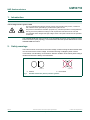
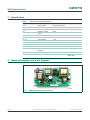
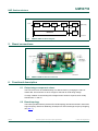
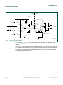
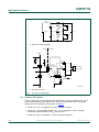
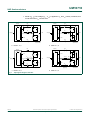
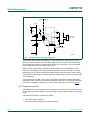
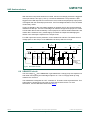
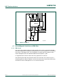
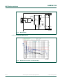
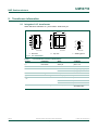
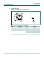
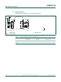
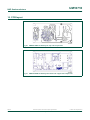
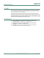
UM10710 UBA20270DB1122 - 35 W/46 V/690 mA LED driver demo board Rev. 2 — 25 September 2013 User manual Document information Info Content Keywords UBA20270DB1122, demo board, LED, non-dimmable, PFC Abstract The UBA20270DB1122 is a non-dimmable 230 V mains 35 W LED driver demo board. It uses a passive PFC topology driving a 46 V/690 mA LED string. Key features: 35 W, isolated, low ripple, small output Electrolytic capacitors UM10710 NXP Semiconductors UBA20270DB1122 - 35 W/46 V/690 mA LED driver demo board Revision history Rev Date Description v.2 20130925 new, updated issue • Modifications: v.1 20130612 Text and graphics updated throughout this user manual. first issue Contact information For more information, please visit: http://www.nxp.com For sales office addresses, please send an email to: [email protected] UM10710 User manual All information provided in this document is subject to legal disclaimers. Rev. 2 — 25 September 2013 © NXP B.V. 2013. All rights reserved. 2 of 25 UM10710 NXP Semiconductors UBA20270DB1122 - 35 W/46 V/690 mA LED driver demo board 1. Introduction WARNING Lethal voltage and fire ignition hazard The non-insulated high voltages that are present when operating this product, constitute a risk of electric shock, personal injury, death and/or ignition of fire. This product is intended for evaluation purposes only. It shall be operated in a designated test area by personnel qualified according to local requirements and labor laws to work with non-insulated mains voltages and high-voltage circuits. This product shall never be operated unattended. The UBA20270DB1122 demo board is a non-dimmable LED driver using a passive Power Factor Correction (PFC) topology. This manual describes the specification and use of the UBA20270DB1122 board. 2. Safety warnings The board must be connected to the mains voltage. Avoid touching the demo board while it is connected to the mains voltage. An isolated housing is obligatory when used in uncontrolled, non-laboratory environments. Galvanic isolation of the mains phase using a variable transformer is always recommended. 019aab174 019aab173 a. Isolated Fig 1. UM10710 User manual b. Not isolated Variable transformer (Variac) isolation symbols All information provided in this document is subject to legal disclaimers. Rev. 2 — 25 September 2013 © NXP B.V. 2013. All rights reserved. 3 of 25 UM10710 NXP Semiconductors UBA20270DB1122 - 35 W/46 V/690 mA LED driver demo board 3. Specification Table 1. Specification for the demo board Symbol Parameter Values Vmains mains voltage 200 V to 260 V (AC) Iinrush inrush current 12 A 230 V (AC) 230 V (AC) td(on) turn-on delay time 30 ms Po(max) maximum output power 50 W Vo output voltage 40 V to 50 V (AC) Description Io output current 0.690 A Io/Vmains line regulation <3% 230 V (AC) Io/Vo load regulation <2% efficiency 86 % PF power factor 0.96 230 V (AC) THD total harmonic distortion 22 % 230 V (AC) Pi input power 35 W 230 V (AC) T temperature 20 C to +85 C operating range; 230 V (AC) 230 V (AC) 4. Board photograph and block diagram Fig 2. UM10710 User manual UBA20270DB1122 board photograph All information provided in this document is subject to legal disclaimers. Rev. 2 — 25 September 2013 © NXP B.V. 2013. All rights reserved. 4 of 25 UM10710 NXP Semiconductors UBA20270DB1122 - 35 W/46 V/690 mA LED driver demo board (0, ),/7(5 PDLQV 3)& +% /& 7$1. /(' 287387 /('VWULQJ LVRODWLRQ 8%$ /(' 287387 DDD Fig 3. UBA20270DB1122 block diagram 5. Board connections Fig 4. UBA20270DB1122 board connections 6. Functional description 6.1 Output stage component values The LED current can be modified easily to a desired value by changing the value of resistor R6. The board has a 20 % margin to deal with an LED string voltage. If a large variation to the existing LED voltage/current values is required, then modify transformers T1 and T2. 6.2 Board topology The board operates with the passive PFC DCM topology described in detail in Advanced High-Frequency Electronic Ballasting Techniques for Gas Discharge Lamps by Fengfeng Tao (Ref. 1). UM10710 User manual All information provided in this document is subject to legal disclaimers. Rev. 2 — 25 September 2013 © NXP B.V. 2013. All rights reserved. 5 of 25 UM10710 NXP Semiconductors UBA20270DB1122 - 35 W/46 V/690 mA LED driver demo board SULPDU\ VHFRQGDU\ 9%86 ' 1 & ) 9 ' 1 ' 1 9LQ &G Q) 4 9$&PDLQV &UHV 7$ ' P+ - [+ /S + ' /SXPS &B(0, /B(0, 9LQ &G Q) ' 1 7 ( + &21VFUHZ IHHGEDFNFRQWURO ' 1 &B2XW + 4 + /('VWULQJ 9P$ ' 5VHQVH 1 DDD Fig 5. Large signal path of board The voltages Vin1, Vin2 are each half the value of the momentary rectified mains input voltage. The circuit can be seen as split into two separate circuits, one circuit that acts as PFC and one that drives the LED string. They run on the same frequency because they share the half-bridge. In a conventional two stage solution, the PFC and the load each have their own separate operating frequency. UM10710 User manual All information provided in this document is subject to legal disclaimers. Rev. 2 — 25 September 2013 © NXP B.V. 2013. All rights reserved. 6 of 25 UM10710 NXP Semiconductors UBA20270DB1122 - 35 W/46 V/690 mA LED driver demo board ' LLQUHF &HOO 9LQ 6 ' /E 9LQUHF 9% &HOO 6 9LQ ' ' DDD a. Board PFC large signal path SULPDU\ VHFRQGDU\ 9%86 & ) 9 4 7$ &UHV ' P+ - [+ /S + ' + &B2XW + /('VWULQJ 9P$ &21VFUHZ 4 7 ( + IHHGEDFNFRQWURO 5VHQVH DDD b. LED load LLC tank Fig 6. PLC and LLC separated 6.3 Passive PFC boost The PFC stage can be considered as two DCM boost converters operated 180 out of phase and sharing the boost inductor. For the PFC stage, there are four topological stages over one switching cycle as shown in Figure 7. • Mode 1 [t0, t1] Vin1 is applied to Lb and iLb linearly increases • Mode 2 [t1, t2] The negative voltage (Vb Vin1) is applied to Lb and iLb linearly decreases, this mode ends when iLb reaches zero • Mode 3 [t2, t3] Vin2 is applied to Lb and iLb linearly decreases UM10710 User manual All information provided in this document is subject to legal disclaimers. Rev. 2 — 25 September 2013 © NXP B.V. 2013. All rights reserved. 7 of 25 UM10710 NXP Semiconductors UBA20270DB1122 - 35 W/46 V/690 mA LED driver demo board • Mode 4 [t3, t4] The voltage (Vb Vin2) is applied to Lb and iLb linearly increases, this mode ends when iLb reaches zero ' LLQUHF ' LLQUHF 9LQ 6 9LQ ' /E 9LQUHF 9/E 6 9% L/E 6 9LQ 9LQUHF 9/E ' 9% L/E 6 9LQ ' ' ' DDD DDD a. Mode 1: t0, t1 b. Mode 2: t1, t2 ' LOQUHF 6 9LQ ' 9/E L/E 9OQUHF ' LLQUHF 9OQ 9% 6 9OQ ' 6 9/E 9LQUHF ' L/E 9% 6 9LQ ' ' ' G>WW@ DDD c. Mode 3: t2, t3 Fig 7. ' /E DDD d. Mode 4: t3, t4 Topological stages of the PFC UM10710 User manual All information provided in this document is subject to legal disclaimers. Rev. 2 — 25 September 2013 © NXP B.V. 2013. All rights reserved. 8 of 25 UM10710 NXP Semiconductors UBA20270DB1122 - 35 W/46 V/690 mA LED driver demo board 9/E 9LQUHF W 9%9LQUHF L/E ,SN W WF WG LLQUHF W W Fig 8. W W W W DDD Key switching waveform of the PFC The exact equations for the input power versus Vmains, Vb, frequency and the value of Lb can be found in Advanced High-Frequency Electronic Ballasting Techniques for Gas Discharge Lamps by Fengfeng Tao (Ref. 1). For 35 W input power, 230 V and 45 kHz the inductor must have a value of 1.2 mH as on the board. If a higher power is required, the inductor must be lowered in value. If less power is given to the LED load, the inductor value must be increased. In the passive PFC topology, the bus voltage and frequency stabilize at a point where the input power equals the output power + losses. Changing the pump inductor value for 20 % of the nominal power is not required. The UBA20270 feedback control system can increase or decrease the operating frequency to compensate for the different load. 6.4 LLC resonant tank The LED string is driven with a so called LLC half-bridge resonant tank topology. UM10710 User manual All information provided in this document is subject to legal disclaimers. Rev. 2 — 25 September 2013 © NXP B.V. 2013. All rights reserved. 9 of 25 UM10710 NXP Semiconductors UBA20270DB1122 - 35 W/46 V/690 mA LED driver demo board SULPDU\ VHFRQGDU\ 9%86 & ) 9 4 7$ &UHV ' P+ - [+ /S + ' + &B2XW + /('VWULQJ 9P$ &21VFUHZ 4 7 ( + IHHGEDFNFRQWURO 5VHQVH DDD Fig 9. Resonant tank for driving the LED string The resonant tank consists of transformer T1 and capacitor C2. More primary current flowing through T1 means more secondary (LED) current is flowing. The resonant tank current depends on the bus voltage and the frequency. Transformer T1 has a relatively large leakage inductance dominating the current. What is unique in this design compared to other LED drivers is the feedback control. Instead of a secondary circuit with operational amplifiers and an optocoupler, a current transformer (T2) is used to generate a feedback signal of the actual LED current. Using resistor R6, the LED current is transformed into a voltage for the current sense input (CSI) of the UBA20270. The equations for the LED current versus bus voltage, transformer leakage inductance and transfer ratio, frequency and resonant capacitor value can be found in Multi-Channel Constant Current (MC3) LED Driver for Indoor LED Luminaries by Haoran Wu (Ref. 2). 6.5 Protection circuits The UBA20270 IC has two inputs that can be used for protection. One is pulling down the CP pin causing a latched standby. The other option is pulling down the DCI pin causing a reset. There are two protection circuits on the board: • LED overvoltage protection • Bus (electrolytic capacitor) overvoltage protection UM10710 User manual All information provided in this document is subject to legal disclaimers. Rev. 2 — 25 September 2013 © NXP B.V. 2013. All rights reserved. 10 of 25 UM10710 NXP Semiconductors UBA20270DB1122 - 35 W/46 V/690 mA LED driver demo board With the board component values as mounted, the bus overvoltage protection is triggered if the input mains is too high (> 270 V). It resets the UBA20270. The protection is also triggered if an LED output short circuit event occurs, because the pumped up input power is far higher than the used output power then. If an overvoltage situation occurs, the board continuously resets. If going to standby in this overvoltage situation is required, the CP pin can be pulled low instead of the DCI pin. The LED overvoltage can also be configured via jumper 3 to cause a reset rather than a latched standby. For this purpose, the board contains diode D21 and resistor R21. Otherwise every restart slightly increases the output level damaging the diodes or the electrolytic capacitor in the output circuit. For LED output short circuit protection, mount diodes D19 and D20. The diodes avoid a voltage spike on the CSI pin of the UBA20270 at start-up which is too high. - MXPSHU &3 5 9'' 1 5 Nȍ ' '&, 9 7% ((3 & Q) 9 & Q) 9 5 Nȍ 5 Nȍ 4 1 5 5 5 Nȍ Nȍ Nȍ ' 5 Nȍ ' ' 9 Nȍ 9 4 1 9EXV 5 Nȍ 5 Nȍ & Q) 9 8%$UHVHWV RQSULPDU\ RYHUYROWDJH DDD Fig 10. Protection circuit 6.6 UBA20270 circuit The low-voltage VDD of the UBA20270 is generated with a charge pump via capacitor C5 and diode D15 requiring the half-bridge output to run. The VDD supply starts up using resistors R11 and R13. The UBA20270 is designed as a CFL controller IC. Therefore it has a preheat timer. This preheat time is shortened to just a few ms using the R10/C20 circuit. For more information, see the UBA20270 data sheet (Ref. 3). UM10710 User manual All information provided in this document is subject to legal disclaimers. Rev. 2 — 25 September 2013 © NXP B.V. 2013. All rights reserved. 11 of 25 UM10710 NXP Semiconductors UBA20270DB1122 - 35 W/46 V/690 mA LED driver demo board 7%) 9 QP 6/6 */6 3*1' &) 0', &, 9'' & S) 9 5 ȍ 8 & 5 Nȍ 5 Nȍ 55() & Q) 9 '&, *+6 +%2 &6, 6*1' &% &3 '&, &6, )6 8%$ & Q)9 & S) 9 & Q) 9 5 Nȍ & Q) 9 DDD Fig 11. UBA20270 subcircuit 6.7 ElectroMagnetic Interference (EMI) filter 6.7.1 EMI circuit The ground of the bridge rectifier is not the ground of the circuit. A common-mode filter with more suppression is required for this passive PFC circuit compared to a conventional active PFC + half-bridge circuit. The combination of resistor R22 and capacitor C26 is used to dissipate some of the differential EMI noise that passes L_EMI. L2 suppresses the common-mode noise using capacitors C1 and C25. The board requires either the protective earth to be connected, to be used on top of a conducting plate or inside a metal box. One of the corners has a track that ensures easy connection to such a metal plate at 1 cm to 3 cm from the PCB. UM10710 User manual All information provided in this document is subject to legal disclaimers. Rev. 2 — 25 September 2013 © NXP B.V. 2013. All rights reserved. 12 of 25 UM10710 NXP Semiconductors UBA20270DB1122 - 35 W/46 V/690 mA LED driver demo board - [P+ ) IXVH & Q) 9$& / ' 1 & Q) 9$& ' 1 5 ȍ & Q) 9$& /B(0, P+ & Q) 9 & S) N9 ' 1 ' 1 DDD Fig 12. EMI subcircuit 6.7.2 Conducted EMI results Fig 13. EMI with PE connected; no metal shielding UM10710 User manual All information provided in this document is subject to legal disclaimers. Rev. 2 — 25 September 2013 © NXP B.V. 2013. All rights reserved. 13 of 25 UM10710 NXP Semiconductors UBA20270DB1122 - 35 W/46 V/690 mA LED driver demo board Fig 14. EMI in a metal box Fig 15. EMI in a metal box with the board running on a lower frequency As can be seen in the EMI plot, the third harmonic of the operating frequency is crossing the limit line. For this purpose, the operating frequency must be lowered. Small capacitors over diodes D1and D2 at the input stage avoid ringing of inductor LBoost which causes EMI. A small resistor/capacitor combination over the output Schottky diodes D8 and D10 stops ringing in the LLC secondary stage. UM10710 User manual All information provided in this document is subject to legal disclaimers. Rev. 2 — 25 September 2013 © NXP B.V. 2013. All rights reserved. 14 of 25 UM10710 NXP Semiconductors UBA20270DB1122 - 35 W/46 V/690 mA LED driver demo board 6.8 Mains harmonic distortion The board is compliant to Class C. However, it must be made to operate at 35 kHz to 45 kHz instead of 45 kHz to 55 kHz as it is now (see Section 11). Table 2. Harmonic distortion at 35 kHz to 45 kHz Harmonic distortion (%) Class C limit (%) Measured value (%) 3 30 * = 28.8 19.9 5 10 7.6 7 7 4.5 9 5 3.7 11 3 2.7 13 3 2.7 15 to 39 <3 < 2.3 The 11/13 harmonics are marginal. They can be further improved by reducing the capacitance in the EMI filter. 6.9 Measuring on the board Use fully mains isolated measurement equipment (battery operated or differential mode) when evaluating/modifying the board. The ground connection of a normal oscilloscope to the ground connection of the UBA20270 circuit adds a charge pump to the circuit modifying its properties. The addition of a charge pump is related to the Y-cap (1 nF to 2.2 nF) present in every oscilloscope. UM10710 User manual All information provided in this document is subject to legal disclaimers. Rev. 2 — 25 September 2013 © NXP B.V. 2013. All rights reserved. 15 of 25 xxxxxxxxxxxxxxxxxxxxx xxxxxxxxxxxxxxxxxxxxxxxxxx xxxxxxx x x x xxxxxxxxxxxxxxxxxxxxxxxxxxxxxx xxxxxxxxxxxxxxxxxxx xx xx xxxxx xxxxxxxxxxxxxxxxxxxxxxxxxxx xxxxxxxxxxxxxxxxxxx xxxxxx xxxxxxxxxxxxxxxxxxxxxxxxxxxxxxxxxxx xxxxxxxxxxxx x x xxxxxxxxxxxxxxxxxxxxx xxxxxxxxxxxxxxxxxxxxxxxxxxxxxx xxxxx xxxxxxxxxxxxxxxxxxxxxxxxxxxxxxxxxxxxxxxxxxxxxxxxxx xxxxxxxx xxxxxxxxxxxxxxxxxxxxxxxxx xxxxxxxxxxxxxxxxxxxx xxx NXP Semiconductors UM10710 User manual 7. Schematic SULPDU\ ; FKDVVLV - ) IXVH [P+ ' 1 / & Q) 9$& & Q) 9$& ' 1 & Q) 9$& P+ & ' P+ [+ /S + + 5 Nȍ ȍ + & ) 9 + $ - & Q) 9 QP ' 9 5 ȍ /('VWULQJ 9 P$ &21 VFUHZ Q) 9 &6, ' 9'' 9 QP ' 5 ȍ ' 9 9 QP QP 6/6 */6 3*1' &) 0', &, 9'' & S) 9 5 ȍ 8 1 5 ȍ /B(0, 6736 & 5 + & ' 5 5 Nȍ ' QP 5 QP 7 ( SODFHZLUHSLQ QP & S) 9 ' 55() & Q) 9 ' 4 63$1& ȍ ' & QP 1 ; VKLHOG & Q) 9 & Q) 9 7$ ((3 & ) 9 9'' 5 ȍ 6736 ORZORVV 4 63$1& S) 9 ' 1 9%86 & Q) 9 & Q) 9 VHFRQGDU\ & Q) N9 <FDS *+6 )6 +%2 &6, 6*1' &% &3 &6, '&, 8%$ - MXPSHU & '&, Q)9 & S) 9 5 Nȍ & Q) 9 ' 5 Nȍ & 7% Q) ((3 9 1 5 9'' Nȍ '&, & Q) 9 ' 9 5 Nȍ 5 Nȍ 4 1 5 5 Nȍ Nȍ 9%86 ' 9 4 1 ' 5 Nȍ 9 5 Nȍ 5 Nȍ & Q) 9 8%$ZLOOUHVHW RQSULPDU\ RYHUYROWDJH DDD UM10710 16 of 25 © NXP B.V. 2013. All rights reserved. 8%$ZLOOUHVHWRU VZLWFKWRVWDQGE\RQ VHFRQGDU\RYHUYROWDJH Fig 16. UBA20270DB1122 schematic diagram 9'' NȍQP Nȍ 5 1QP & Q) 9 ' 5 UBA20270DB1122 - 35 W/46 V/690 mA LED driver demo board Rev. 2 — 25 September 2013 All information provided in this document is subject to legal disclaimers. & ' S) 1 N9 & Q) 9 /B(0, & Q) 9 & S) 9 P+ OUPV P$(( ' S)9 & Q) 9 1 ' 5 ȍ /SXPS UM10710 NXP Semiconductors UBA20270DB1122 - 35 W/46 V/690 mA LED driver demo board 8. Bill Of Material (BOM) Table 3. Bill of material Reference Description and values Part number Manufacturer C1; C13 C2 capacitor; 2.2 nF; 20 %; 250 V; X1/Y2 DE2E3KY222MA3BM02 Murata capacitor; 18 nF; 10 %; 600 V B32672L1183K EPCOS C3; C7; C16 capacitor; 100 nF; 5 %; 450 V ECWF2W104JAQ Panasonic C4 capacitor; 10 F; 10 %; 450 V ECA2WM100 Panasonic C5 capacitor; 330 pF; 10 %; 630 V; 1206; X7R MCCA000760 Multicomp C6 capacitor; 470 nF; 10 %; 50 V; 1206; X7R ESD55C474K4T2A-26 AVX C8 capacitor; not mounted - - C9; C10 capacitor; 1 nF; 10 %; 200 V; 0603; X7R 06032C102KAT2A AVX C12 capacitor; 100 F; 100 V; 10 % ECA-2AM101 Panasonic C14 capacitor; 10 nF; 10 %; 16 V; 0603; X7R MC0603B103M160CT Multicomp C15; C26 capacitor; 47 nF; 10 %; 275 V BFC233820473 Vishay C17 capacitor; 100 nF; +80 %/20 %; 50 V; 0603; Y5V MC0603F104Z500CT Multicomp C18 capacitor; 22 nF; 10 %; 25 V; 0603; X7R MCCA000169 Multicomp C19 capacitor; 47 nF; 10 %; 50 V; 0603; X7R MC0603B473K500CT Multicomp C20; C22 capacitor; 100 pF; 5 %; 50 V; 0603; NP0 MCCA000204 Multicomp C21 capacitor; 47 nF; 10 %; 25 V; 0603; X7R 06033C473JAT2A C23; C24 capacitor; 3.3 pF; 10 %; 500 V; 0805; C0G MC0805N3R3C501CT Multicomp C25 capacitor; 470 pF; 10 %; 2 kV DEHR33D471KA3B Murata C27 capacitor; 47 nF; 20 %; 275 V (AC) ECQ-U2A473ML Panasonic C30 capacitor; 1 nF; 20 %; 50 V; 0603 MC0603B102M500CT Multicomp C31 capacitor; 10 nF; 50 V 06031C103JAT2A AVX D1; D2; D3; D4; D6; D7 fast diode; 1 A; 600 V 1N4937G Multicomp D8; D10 Schottky diode; 150 V; 1 A STPS1150 ST D13; D15 high-speed diode; SOD-80C PMLL4148L NXP Semiconductors D16 Zener diode; 0.5 W; 13 V BZV55-C13 NXP Semiconductors D17 Zener diode; 0.5 W; 3.3 V PDZ3.3B,115 NXP Semiconductors D18; D22 Zener diode; 0.5 W; 5.6 V BZV55-C5V6 NXP Semiconductors D21 Zener diode; 68 V; 1 W 1SMA4760 Multicomp F1 fast fuse; 2 A 0034.6017 SCHURTER J1 connector; mains inlet CTB5000/3 Camdenboss J2 connector; LED output CTB5000/2 Camdenboss J3 header SL 11/190/ 20/G Fischer Elektronik L2 choke; common-mode; 2 33 mH 7448640405 Würth Elektronik L_EMI choke; 1.5 mH 744772152 Würth Elektronik AVX Lpump choke; 1.2 mH 750313755 Würth Elektronik Q1; Q2 MOSFET-N; 600 V; 7.3 A SPA07N60C3 Infineon Q3; Q4 MOSFET-N; 60 V; 0.19 A; SOT23 NX7002AK NXP Semiconductors UM10710 User manual All information provided in this document is subject to legal disclaimers. Rev. 2 — 25 September 2013 © NXP B.V. 2013. All rights reserved. 17 of 25 UM10710 NXP Semiconductors UBA20270DB1122 - 35 W/46 V/690 mA LED driver demo board Table 3. Bill of material …continued Reference Description and values R01; R02 wire Part number Manufacturer R1 resistor; not mounted - - R2; R18 resistor; 47 ; SMD - - R3 resistor; 330 ; SMD - - R4 resistor; 33 k; SMD - - R5 resistor; 0.22 film; 5 %; 500 mW 1622600-1 TE Connectivity R6 resistor; 8.2 ; 1 %; 250 mW; SMD - - R7 resistor; 2.2 k; SMD - - R8; R20 resistor; 10 k; SMD - - R9 resistor; 1.8 k; SMD - - R10 resistor; 68 k; SMD - - R11 resistor; 110 k - - R13; R16 resistor; 220 k; SMD - - R14 resistor; 27 k; SMD - - R15 resistor; 100 k; SMD - - R17 resistor; 6.2 k; SMD - - R19 resistor; 0 ; SMD - - R21 resistor; 22 ; SMD - - R22 resistor; 120 ; SMD - - R23 resistor; 22 k; SMD - - T1 LLC transformer 750313753_01 Würth Elektronik T2 sense transformer 750313754 Würth Elektronik U1 IC half-bridge controller UBA20270T NXP Semiconductors UM10710 User manual All information provided in this document is subject to legal disclaimers. Rev. 2 — 25 September 2013 © NXP B.V. 2013. All rights reserved. 18 of 25 UM10710 NXP Semiconductors UBA20270DB1122 - 35 W/46 V/690 mA LED driver demo board 9. Transformer information 9.1 Integrated LLC transformer Wurth Electronics Midcom Inc.; part number: 750313753_01. PD[ PD[ SUL VHF VHF DX[ 'LPHQVLRQVDUHLQPP ORWFRGH DDD DDD a. Side view b. Top view DDD c. Winding pinout Fig 17. LLC transformer Table 4. LLC transformer electrical specifications Symbol Parameter Value Condition Lp inductance 3400 H pins 1 to 2 Isat saturation current 1.27 A N turns ratio 4.25 (1-2):(6-7) (1-2):(6-7) 6.18 (1-2):(3-4) Llk leakage inductance 870 H tie 6 + 7 + 8 V dielectric rating 1250 V (AC) pins 1 to 8 RDC DC resistance 1590 m pins 1 to 2 238 m pins 6 to 7 and 7 to 8 720 m pins 3 to 4 1250 V (AC) between primary and secondary side dielectric rating UM10710 User manual All information provided in this document is subject to legal disclaimers. Rev. 2 — 25 September 2013 © NXP B.V. 2013. All rights reserved. 19 of 25 UM10710 NXP Semiconductors UBA20270DB1122 - 35 W/46 V/690 mA LED driver demo board 9.2 Sense transformer Wurth Electronics Midcom Inc.; part number 750313754 GRWORFDWHVWHUP PD[ PD[ SUL VHF VHF 'LPHQVLRQVDUHLQPP DDD DDD a. Top view b. Winding pinout Fig 18. Sense transformer Table 5. UM10710 User manual Sense transformer electrical specifications Symbol Parameter Value Condition Lp inductance 150 H pins 1 to 3 Llk leakage inductance < 4 H tie pins (5 + 6 + 7 + 8) N turns ratio 6.666 (1-3):(5-7); (1-3):(6-8) RDC DC resistance 470 m pins 1 to 3 15 m pins 5 to 7 15 m pins 6 to 8 All information provided in this document is subject to legal disclaimers. Rev. 2 — 25 September 2013 © NXP B.V. 2013. All rights reserved. 20 of 25 UM10710 NXP Semiconductors UBA20270DB1122 - 35 W/46 V/690 mA LED driver demo board 9.3 Pump inductor Wurth Electronics Midcom Inc.; part number 750313755 GRWORFDWHVWHUP $ PD[ PD[ PD[ ORWFRGHDQGGDWHFRGH 'LPHQVLRQVDUHLQPP DDD a. Top/side view DDD b. Winding pinout Fig 19. Pump inductor Table 6. UM10710 User manual Sense transformer electrical specifications Symbol Parameter Value Condition Lp inductance 1200 H pins 1 to 10 Isat saturation current 1A RDC DC resistance 510 m All information provided in this document is subject to legal disclaimers. Rev. 2 — 25 September 2013 pins 1 to 10 © NXP B.V. 2013. All rights reserved. 21 of 25 UM10710 NXP Semiconductors UBA20270DB1122 - 35 W/46 V/690 mA LED driver demo board 10. PCB layout Fig 20. UBA20270DB1122 PCB layout: top side components Fig 21. UBA20270DB1122 PCB layout bottom side copper and components UM10710 User manual All information provided in this document is subject to legal disclaimers. Rev. 2 — 25 September 2013 © NXP B.V. 2013. All rights reserved. 22 of 25 UM10710 NXP Semiconductors UBA20270DB1122 - 35 W/46 V/690 mA LED driver demo board 11. Errata With the current PCB, it can happen that the ballast does not start at a quick on/off/on cycle. To fix this issue, connect the VDD start-up resistor R13 to the anode of D2. At the same time increase resistor R11 to 220 k. The board EMI spectrum shows a peak at 150 kHz which is on the edge of the limit (depending on the exact load and mains voltage). Its 11th and 13th harmonic are also on the limit. Both problems can be solved by running the board on a lower frequency. To run the board on a lower frequency, increase the LBoost to 1.4 mH. At the same time increase capacitor C22 (CF pin UBA20270) from 100 pF to 120 pF. 12. References UM10710 User manual [1] Advanced High-Frequency Electronic Ballasting Techniques for Gas Discharge Lamps — Fengfeng Tao, 19 December 2001 [2] Multi-Channel Constant Current (MC3) LED Driver for Indoor LED Luminaries — Haoran Wu, 14 November 2011 [3] UBA20270 — 600 V Driver IC for dimmable compact fluorescent lamps; 8 September 2011; Copyright: NXP Semiconductors All information provided in this document is subject to legal disclaimers. Rev. 2 — 25 September 2013 © NXP B.V. 2013. All rights reserved. 23 of 25 UM10710 NXP Semiconductors UBA20270DB1122 - 35 W/46 V/690 mA LED driver demo board 13. Legal information 13.1 Definitions Draft — The document is a draft version only. The content is still under internal review and subject to formal approval, which may result in modifications or additions. NXP Semiconductors does not give any representations or warranties as to the accuracy or completeness of information included herein and shall have no liability for the consequences of use of such information. Export control — This document as well as the item(s) described herein may be subject to export control regulations. Export might require a prior authorization from competent authorities. 13.2 Disclaimers Limited warranty and liability — Information in this document is believed to be accurate and reliable. However, NXP Semiconductors does not give any representations or warranties, expressed or implied, as to the accuracy or completeness of such information and shall have no liability for the consequences of use of such information. NXP Semiconductors takes no responsibility for the content in this document if provided by an information source outside of NXP Semiconductors. In no event shall NXP Semiconductors be liable for any indirect, incidental, punitive, special or consequential damages (including - without limitation - lost profits, lost savings, business interruption, costs related to the removal or replacement of any products or rework charges) whether or not such damages are based on tort (including negligence), warranty, breach of contract or any other legal theory. Notwithstanding any damages that customer might incur for any reason whatsoever, NXP Semiconductors’ aggregate and cumulative liability towards customer for the products described herein shall be limited in accordance with the Terms and conditions of commercial sale of NXP Semiconductors. Right to make changes — NXP Semiconductors reserves the right to make changes to information published in this document, including without limitation specifications and product descriptions, at any time and without notice. This document supersedes and replaces all information supplied prior to the publication hereof. Suitability for use — NXP Semiconductors products are not designed, authorized or warranted to be suitable for use in life support, life-critical or safety-critical systems or equipment, nor in applications where failure or malfunction of an NXP Semiconductors product can reasonably be expected to result in personal injury, death or severe property or environmental damage. NXP Semiconductors and its suppliers accept no liability for inclusion and/or use of NXP Semiconductors products in such equipment or applications and therefore such inclusion and/or use is at the customer’s own risk. Applications — Applications that are described herein for any of these products are for illustrative purposes only. NXP Semiconductors makes no representation or warranty that such applications will be suitable for the specified use without further testing or modification. Customers are responsible for the design and operation of their applications and products using NXP Semiconductors products, and NXP Semiconductors accepts no liability for any assistance with applications or customer product design. It is customer’s sole responsibility to determine whether the NXP Semiconductors product is suitable and fit for the customer’s applications and products planned, as well as for the planned application and use of customer’s third party customer(s). Customers should provide appropriate design and operating safeguards to minimize the risks associated with their applications and products. UM10710 User manual NXP Semiconductors does not accept any liability related to any default, damage, costs or problem which is based on any weakness or default in the customer’s applications or products, or the application or use by customer’s third party customer(s). Customer is responsible for doing all necessary testing for the customer’s applications and products using NXP Semiconductors products in order to avoid a default of the applications and the products or of the application or use by customer’s third party customer(s). NXP does not accept any liability in this respect. Evaluation products — This product is provided on an “as is” and “with all faults” basis for evaluation purposes only. NXP Semiconductors, its affiliates and their suppliers expressly disclaim all warranties, whether express, implied or statutory, including but not limited to the implied warranties of non-infringement, merchantability and fitness for a particular purpose. The entire risk as to the quality, or arising out of the use or performance, of this product remains with customer. In no event shall NXP Semiconductors, its affiliates or their suppliers be liable to customer for any special, indirect, consequential, punitive or incidental damages (including without limitation damages for loss of business, business interruption, loss of use, loss of data or information, and the like) arising out the use of or inability to use the product, whether or not based on tort (including negligence), strict liability, breach of contract, breach of warranty or any other theory, even if advised of the possibility of such damages. Notwithstanding any damages that customer might incur for any reason whatsoever (including without limitation, all damages referenced above and all direct or general damages), the entire liability of NXP Semiconductors, its affiliates and their suppliers and customer’s exclusive remedy for all of the foregoing shall be limited to actual damages incurred by customer based on reasonable reliance up to the greater of the amount actually paid by customer for the product or five dollars (US$5.00). The foregoing limitations, exclusions and disclaimers shall apply to the maximum extent permitted by applicable law, even if any remedy fails of its essential purpose. Safety of high-voltage evaluation products — The non-insulated high voltages that are present when operating this product, constitute a risk of electric shock, personal injury, death and/or ignition of fire. This product is intended for evaluation purposes only. It shall be operated in a designated test area by personnel that is qualified according to local requirements and labor laws to work with non-insulated mains voltages and high-voltage circuits. The product does not comply with IEC 60950 based national or regional safety standards. NXP Semiconductors does not accept any liability for damages incurred due to inappropriate use of this product or related to non-insulated high voltages. Any use of this product is at customer’s own risk and liability. The customer shall fully indemnify and hold harmless NXP Semiconductors from any liability, damages and claims resulting from the use of the product. Translations — A non-English (translated) version of a document is for reference only. The English version shall prevail in case of any discrepancy between the translated and English versions. 13.3 Trademarks Notice: All referenced brands, product names, service names and trademarks are the property of their respective owners. All information provided in this document is subject to legal disclaimers. Rev. 2 — 25 September 2013 © NXP B.V. 2013. All rights reserved. 24 of 25 UM10710 NXP Semiconductors UBA20270DB1122 - 35 W/46 V/690 mA LED driver demo board 14. Contents 1 2 3 4 5 6 6.1 6.2 6.3 6.4 6.5 6.6 6.7 6.7.1 6.7.2 6.8 6.9 7 8 9 9.1 9.2 9.3 10 11 12 12.1 12.2 12.3 13 Introduction . . . . . . . . . . . . . . . . . . . . . . . . . . . . 3 Safety warnings . . . . . . . . . . . . . . . . . . . . . . . . . 3 Specification. . . . . . . . . . . . . . . . . . . . . . . . . . . . 4 Board photograph and block diagram. . . . . . . 4 Board connections . . . . . . . . . . . . . . . . . . . . . . 5 Functional description . . . . . . . . . . . . . . . . . . . 5 Output stage component values . . . . . . . . . . . . 5 Board topology . . . . . . . . . . . . . . . . . . . . . . . . . 5 Passive PFC boost . . . . . . . . . . . . . . . . . . . . . . 7 LLC resonant tank . . . . . . . . . . . . . . . . . . . . . . 9 Protection circuits . . . . . . . . . . . . . . . . . . . . . . 10 UBA20270 circuit . . . . . . . . . . . . . . . . . . . . . . 10 ElectroMagnetic Interference (EMI) filter . . . . 11 EMI circuit . . . . . . . . . . . . . . . . . . . . . . . . . . . . 11 Conducted EMI results . . . . . . . . . . . . . . . . . . 12 Mains harmonic distortion. . . . . . . . . . . . . . . . 14 Measuring on the board . . . . . . . . . . . . . . . . . 14 Schematic . . . . . . . . . . . . . . . . . . . . . . . . . . . . . 15 Bill Of Material (BOM) . . . . . . . . . . . . . . . . . . . 16 Transformer information . . . . . . . . . . . . . . . . . 18 Integrated LLC transformer . . . . . . . . . . . . . . 18 Sense transformer . . . . . . . . . . . . . . . . . . . . . 19 Pump inductor . . . . . . . . . . . . . . . . . . . . . . . . 20 PCB layout . . . . . . . . . . . . . . . . . . . . . . . . . . . . 21 Errata. . . . . . . . . . . . . . . . . . . . . . . . . . . . . . . . . 22 Legal information. . . . . . . . . . . . . . . . . . . . . . . 23 Definitions . . . . . . . . . . . . . . . . . . . . . . . . . . . . 23 Disclaimers . . . . . . . . . . . . . . . . . . . . . . . . . . . 23 Trademarks. . . . . . . . . . . . . . . . . . . . . . . . . . . 23 Contents . . . . . . . . . . . . . . . . . . . . . . . . . . . . . . 24 Please be aware that important notices concerning this document and the product(s) described herein, have been included in section ‘Legal information’. © NXP B.V. 2013. All rights reserved. For more information, please visit: http://www.nxp.com For sales office addresses, please send an email to: [email protected] Date of release: 25 September 2013 Document identifier: UM10710