1
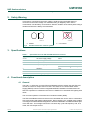
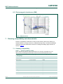
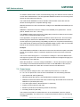
UM10560 230 V 7 W flyback converter SSL2101 reference board Rev. 1 — 20 August 2012 User manual Document information Info Content Keywords SSL2101, dimmable, LED driver, flyback converter, GU10 Abstract This document describes the operation of a 230 V 7 W dimmable LED driver featuring SSL2101 and using a flyback topology. The SSL2101DB1069 reference board has a form factor that is compatible with the base of a GU10 LED lamp fitting used in Solid-State Lighting (SSL) applications. UM10560 NXP Semiconductors 230 V 7 W flyback converter SSL2101 reference board Revision history Rev Date Description v.1 20120820 first issue Contact information For more information, please visit: http://www.nxp.com For sales office addresses, please send an email to: [email protected] UM10560 User manual All information provided in this document is subject to legal disclaimers. Rev. 1 — 20 August 2012 © NXP B.V. 2012. All rights reserved. 2 of 22 UM10560 NXP Semiconductors 230 V 7 W flyback converter SSL2101 reference board 1. Introduction WARNING Lethal voltage and fire ignition hazard The non-insulated high voltages that are present when operating this product, constitute a risk of electric shock, personal injury, death and/or ignition of fire. This product is intended for evaluation purposes only. It shall be operated in a designated test area by personnel qualified according to local requirements and labor laws to work with non-insulated mains voltages and high-voltage circuits. This product shall never be operated unattended. This document describes the operation of a 230 V 7 W dimmable LED driver featuring the SSL2101. The SSL2101DB1069 reference board has a GU10 LED lamp compatible form factor. The flyback converter topology provides a simple and efficient solution for mains dimmable LED recessed light applications. The total input power (VA) to the board is 230 V/52 mA = 11.9 W. The SSL2101DB1069 reference board is designed to drive a 5-LED load, delivering an output power of 6.7 W with 16.3 V/410 mA. The Power Factor (PF) is 0.75 which gives an actual input power of 0.75 11.9 W = 8.9 W and the resulting efficiency is 75 %. The SSL2101DB1069 reference board complies with EMI and safety regulations. The SSL2101DB1069 reference board is designed so the components allow enough headroom for the board to fit into a GU10 lamp base. The board dimensions are shown in Figure 1.The assembled top board view is shown in Figure 2 and the bottom board view in Figure 3. PP PP PP PP PP DDD Fig 1. UM10560 User manual SSL2101DB1069 Reference board dimensions All information provided in this document is subject to legal disclaimers. Rev. 1 — 20 August 2012 © NXP B.V. 2012. All rights reserved. 3 of 22 UM10560 NXP Semiconductors 230 V 7 W flyback converter SSL2101 reference board UM10560 User manual Fig 2. SSL2101DB1069 Reference board (top view) Fig 3. SSL2101DB1069 Reference board (bottom view) All information provided in this document is subject to legal disclaimers. Rev. 1 — 20 August 2012 © NXP B.V. 2012. All rights reserved. 4 of 22 UM10560 NXP Semiconductors 230 V 7 W flyback converter SSL2101 reference board 2. Safety Warning This board is connected to the mains voltage. Avoid touching the board while it is connected to the mains voltage. An isolated housing is obligatory when used in uncontrolled, non-laboratory environments. Galvanic isolation of the mains phase using a variable transformer is always recommended. 019aab174 019aab173 a. isolated Fig 4. b. non-isolated Variable transformer isolation symbols 3. Specifications Table 1. Specifications for the SSL2101DB1069 reference board Symbol Parameter Value Vmains AC mains supply voltage 230 V VO output voltage 16.3 V IO output current 410 mA Io/Vo output voltage rejection 22.5 mA/V (2.5 % at nominal IO = 410 mA) efficiency 75 % PF Power Factor 0.75 fSW switching frequency 55 kHz 4. Functional description 4.1 General The 230 V, 7 W flyback converter SSL2101DB1069 reference board uses the SSL2101 control IC to drive an output load of 5-LEDs. The SSL2101 is a Switch Mode Power Supply (SMPS) control IC with an integrated MOSFET. Detailed information about the SSL2101 operation is contained in the SSL2101 SMPS IC for dimmable LED lighting data sheet. The converter operates in Discontinuous Conduction Mode (DCM). The SSL2101DB1069 reference board is triac dimmable and can be used in combination with most leading and trailing-edge dimmers. During dimming, the rectified mains voltage is averaged and attenuated and supplied to both the PWMLIMIT and BRIGHTNESS pins of the SSL2101. This voltage reduces the converter duty cycle and frequency and, as a result, the LED output current. UM10560 User manual All information provided in this document is subject to legal disclaimers. Rev. 1 — 20 August 2012 © NXP B.V. 2012. All rights reserved. 5 of 22 UM10560 NXP Semiconductors 230 V 7 W flyback converter SSL2101 reference board Dimming compatibility performance has been tested with a selection of 30 leading/trailing-edge dimmers as shown in Section 7. 5. SSL2101DB1069 reference board connections The GU10 LED driver SSL2101DB1069 reference board takes a 230 V, 50 Hz mains supply and supports a 5-LED load. The board connection is shown in Figure 5. Remark: Make all connections with the input power is switched off. • Connect the 5-LED load as output load together with power meter at both inputs and outputs. • Connect VIN (230 V/50 Hz) using an isolating transformer to the input connection points of the buck converter. Alternatively use an AC power supply with limited output current capability (for example; 200 mA). • Increase VIN to 230 V and measure the different parameters as shown in Table 2. • When testing dimmer compatibility, connect a leading or trailing edge dimmer between VIN and the buck converter input connection points. Remark: Use protective a shield over application and never touch the board when measuring or testing. Table 2. Input/output parameters VIN (V) II (mA) PF PIN (W) VO (V) IO (mA) PO (W) 230 52 0.75 8.9 16.3 410 6.7 0.75 /('V P$ / 9 1 DDD Fig 5. UM10560 User manual Connection to the SSL2101DB1069 reference board All information provided in this document is subject to legal disclaimers. Rev. 1 — 20 August 2012 © NXP B.V. 2012. All rights reserved. 6 of 22 UM10560 NXP Semiconductors 230 V 7 W flyback converter SSL2101 reference board 6. Performance data The performance was measured with 5 LEDs connected as output load. The performance data is shown in Figure 6 to Figure 10. 6.1 Efficiency DDD Ș Fig 6. 9,19 Efficiency as a function of AC mains input voltage 6.2 Line regulation (0.5 %/V) DDD ,2 P$ Fig 7. UM10560 User manual 9,19 Output current as a function of AC mains input voltage All information provided in this document is subject to legal disclaimers. Rev. 1 — 20 August 2012 © NXP B.V. 2012. All rights reserved. 7 of 22 UM10560 NXP Semiconductors 230 V 7 W flyback converter SSL2101 reference board 6.3 Power factor DDD 3) Fig 8. 9,19 Power factor as a function of AC mains input voltage 6.4 Load regulation (2.5 % per volt for nominal IO = 410 mA) DDD ,2 P$ Fig 9. UM10560 User manual 929 Output current as a function of output voltage All information provided in this document is subject to legal disclaimers. Rev. 1 — 20 August 2012 © NXP B.V. 2012. All rights reserved. 8 of 22 UM10560 NXP Semiconductors 230 V 7 W flyback converter SSL2101 reference board 6.5 Electromagnetic Interference (EMI) Fig 10. EMI performance 7. Dimming compatibility and characteristic Dimming compatibility is defined as having smooth dimming without any flashing or flickering effects occurring across the complete dimming range. The SSL2101DB1069 reference board has tested with a selection of trailing and leading-edge dimmers as shown in Table 3. 7.1 Dimming compatibility Table 3. Selection of dimmers tested Due to different manufacturer dimmer specifications, the dimming compatibility may vary With no triac (no dimming) the LED output current is 410 mA which represents 100 % Manufacturer Dimming range Dimming compatibility Leading-edge UM10560 User manual Opus 852390 0.25 % to 100 % good Opus 852392 0.25 % to 100 % good Bush 2250U 0.1 % to 100 % good Bush 2247U 5 % to 100 % good Bush 6519U 23 % to 100 % good Gira 118400 0.25 % to 100 % good EverFlourish PF0700DA 1.2 % to 100 % good HET 3901 0.25 % to 100 0 good Legrand CXM03 0.1 % to100 % good Varilight 1103034 0.1 % to 100 % good Chinese dimmer 1 0.8 % to 100 % good Chinese dimmer 2 0.9 % to 100 % good All information provided in this document is subject to legal disclaimers. Rev. 1 — 20 August 2012 © NXP B.V. 2012. All rights reserved. 9 of 22 UM10560 NXP Semiconductors 230 V 7 W flyback converter SSL2101 reference board Table 3. Selection of dimmers tested …continued Due to different manufacturer dimmer specifications, the dimming compatibility may vary With no triac (no dimming) the LED output current is 410 mA which represents 100 % Manufacturer Dimming range Dimming compatibility Legrand V051 0.1 % to100 % good Chinese dimmer 3 6.5 % to 100 % good Chinese dimmer 4 6 % to 100 % good 11 % to 100 % good Trailing-edge Drespatronic 0817 Drespatronic 0815 5 % to 100 % flicker Berker 286170 9 % to 100 % good Berker 2874 10 % to 100 % good Bush 6591U 0.25 % to 100 % triac on/off Bush 6513U 23 % to 100 % good Jung 225TDE 9 % to 100 % good Jung 243EX 10 % to 100 % good Gira 030700 10 % to 100 % good PEH433HAB 11 % to 100 % good Niko 23 % to 100 % good Legrand CXM02 5 % to 100 % triac on/off at 100 % Legrand 78402 7 % to 100 % good Varilight 1106037 3 % to 100 % good CLIPSAL Universal dimmer 7 % to 100 % good 7.2 Dimming characteristic At 230 V input mains, the voltage divider sets the voltage on the BRIGHTNESS and PWMLIMIT pins and therefore the converter frequency and duty cycle. This divider consists of resistors R7, R8 and R9, together with capacitor C9 for filtering, During dimming, the voltage on the BRIGHTNESS and PWMLIMIT pins decreases. This decrease reduces the converter frequency and duty cycle respectively. The dimming curve of IO against the triac conduction angle for leading and trailing edge dimmers is shown in Figure 11. UM10560 User manual All information provided in this document is subject to legal disclaimers. Rev. 1 — 20 August 2012 © NXP B.V. 2012. All rights reserved. 10 of 22 UM10560 NXP Semiconductors 230 V 7 W flyback converter SSL2101 reference board DDD ,2 P$ &RQGXFWLRQDQJOHPV (1) Leading-edge dimmer (2) Trailing-edge dimmer Fig 11. Dimming curve - LED current as a function of triac conduction angle The SSL2101DB1069 reference board uses the feedback loop on the secondary side to limit the LED output current. Resistors R18 and R18a sense the LED current IO. A current mirror using the BC847S compares ILED to a reference current IREF. VO, R21, R24 and R23 set this current. When IO > IREF, the extra current in the optocoupler limits the on time of the converter. The same feedback loop is also used for overvoltage protection (OVP). OVP begins once VO is greater than the Zener voltage of D8, which here is 20 V. The dimming voltage is detected by sensing the average rectified voltage. After R and R8 limit the double bridge rectifier and the input peak current, capacitors C2 and C3 determine the triac latch current. The mains voltage and current waveforms for a leading-edge dimmer for a conduction angle of 8 ms ( = 4 / 5) are shown in Figure 12. Fig 12. Mains voltage/current waveforms UM10560 User manual All information provided in this document is subject to legal disclaimers. Rev. 1 — 20 August 2012 © NXP B.V. 2012. All rights reserved. 11 of 22 UM10560 NXP Semiconductors 230 V 7 W flyback converter SSL2101 reference board To maintain sufficient triac current over the dimming range, the SSL2101 has two internal current sinks called bleeders. The strong bleeder SBLEED resets the zero crossing of the dimmer and also helps triac latching. The weak bleeder WBLEED is used to maintain sufficient hold current after the triac latches and throughout the complete dimming range. SBLEED is switched on when the maximum voltage on the WBLEED and SBLEED pins is below 52 V. WBLEED is switched on when the voltage on the ISENSE pin is greater than 100 mV (that is, between 0 mV and 100 mV). The ISENSE voltage is derived from the voltage drop across R17 and thus the converter current return to the double bridge rectifier. In this application, an optional circuit is included for extra hold current. The hold current flows through Q1 and R6 when WBLEED is on. The resistor R6 determines the extra current required for good dimming compatibility but there is a compromise with efficiency. The weak bleeder is switched off when the ISENSE voltage exceeds 250 mV. The weak bleeder is also switched off when the strong bleeder is switched on. Example: The weak bleeder is switched on when the current in the converter return path is less than 20 mA. This condition could be a minimum requirement for the hold current of the triac dimmer. The 20 mA current through R17 = 10 results in a voltage of 250 mV at RGND node with respect to ground. R15, R16 and C9 attenuate and filter this voltage and supply it to the ISENSE pin of the SSL2101. When R15 and R16 = 10 k, the voltage at ISENSE is 100 mV with respect to ground. This voltage is the internal threshold level to switch on the WBLEED. In this case, the weak bleeder is switched on when the converter current is less than 20 mA. 7.3 Power losses For an input mains voltage of 230 V, the measured powers are PIN = 8.9 W and PO = 6.7 W. The power loss is 2.2 W which is distributed over the following elements: • input resistors R and R8 (300 mW) • SBLEED resistor R3 when the internal SBLEED is operational (50 mW) • WBLEED resistors R4 and R5 and extra current through Q1 and R6 when the internal WBLEED is operational (600 mW) • • • • core and copper losses in the transformer T1 (400 mW) snubber circuit D2 and D3 (100 mW) MOSFET (conduction and switching losses are 300 mW) secondary diode D4 (450 mW) The hotspot of the PCB is at resistor R6 which is an extra bleeder current to improve dimming compatibility. The value here is a compromise between efficiency and dimming compatibility. UM10560 User manual All information provided in this document is subject to legal disclaimers. Rev. 1 — 20 August 2012 © NXP B.V. 2012. All rights reserved. 12 of 22 UM10560 NXP Semiconductors 230 V 7 W flyback converter SSL2101 reference board The measured temperature of R6 is 75C at 25 C ambient. Reduction in temperature is possible by replacing R6 with a series or parallel connection of two resistors having the same total equivalent resistance value. The measured temperature of the transformer is 55 C at 25C ambient. Finally, the power loss as a function of triac conduction angle for a leading-edge dimmer over the complete dimming range is shown in Figure 13. DDD 3ORVV : FRQGXFWLRQDQJOHPV Fig 13. Power losses as a function of conduction angle UM10560 User manual All information provided in this document is subject to legal disclaimers. Rev. 1 — 20 August 2012 © NXP B.V. 2012. All rights reserved. 13 of 22 xxxx xxxxxxxxxxxxxxxxxxxxxxxxxxxxxx x xxxxxxxxxxxxxx xxxxxxxxxx xxx xxxxxx xxxxxxxxxxxxxxxxxxxxxxx xxxxxxxxxxxxxxxxxxxxxx xxxxx xxxxxx xx xxxxxxxxxxxxxxxxxxxxxxxxxxxxx xxxxxxxxxxxxxxxxxxxxxx xxxxxxxxxxx xxxxxxx xxxxxxxxxxxxxxxxxxx xxxxxxxxxxxxxxxx xxxxxxxxxxxxxx xxxxxx xx xxxxxxxxxxxxxxxxxxxxxxxxxxxxxxxx xxxxxxxxxxxxxxxxxxxxxxxx xxxxxxx xxxxxxxxxxxxxxxxxxxxxxxxxxxxxxxxxxxxxxxxxxxxxx xxxxxxxxxxx xxxxx x x / / 5 P+ ȍ 5 1 / P+ 86*) & Q) 9 5*1' & Q) 9 ' 7 60%%7 ZXUWK ' (6*) ȍ 5 4 =7; Nȍ 8 5 6%/((' Nȍ 5 Nȍ Nȍ 9&& :%/((' 9&& *1' 5 Nȍ *1' 5 5 Nȍ Nȍ %5,*+71(66 5 Nȍ 5 Nȍ & ) 9 5 Nȍ 5& 5& 66/ & S) 9 5 67368 & ) 9 &D ) 9 5 /('6 P$ Pȍ 5D Pȍ '5$,1 *1' *1' 5 ȍ *1' & Q) N9 5 ȍ 5 Nȍ 5 Nȍ 5 Nȍ 6285&( $8; ,6(16( 5 5 Nȍ ' %=9& Nȍ 5 ȍ 3:0/,0,7 ' 30/// ' %$9 5 Nȍ 5 ȍ ' 8 %&%6 9&& & S) 9 5 Nȍ & ) 9 ' %=9& ȍ 5 ȍ 5*1' 8 )2'& Fig 14. Schematic diagram: 230 V 7 W flyback converter using the SSL2101 UM10560 14 of 22 © NXP B.V. 2012. All rights reserved. DDD 230 V 7 W flyback converter SSL2101 reference board Rev. 1 — 20 August 2012 All information provided in this document is subject to legal disclaimers. 5*1' 5 7.4 Schematic & Q) 9 ;FODVV 9 +] NXP Semiconductors UM10560 User manual ' %' %6* UM10560 NXP Semiconductors 230 V 7 W flyback converter SSL2101 reference board 8. Bill of Materials (BOM) Table 4. Bill of Materials Part Reference Description Manufacturer/part number BD1 bridge rectifier; 600 V, 0.8 A Comchip Tech; B6S-G C1 0.010 F; 305 V (AC); 630 V (DC); 20 %; X2 class; EPCOS; B32921C3103M radial; long lead C2 0.47 F; 450 V (DC); 10 %; epoxy coated ceramic; Murata; RDED72W474K5B1 radial C3 0.47 F; 450 V (DC); 10 %; epoxy coated ceramic; Murata; RDED72W474K5B1 radial C6 4.7 F; 50 V; 10 %; X5R ceramic; 1206 Taiyo Yuden; UMK316BJ475KL-T C7 10 F; 25 V; 10 %; X7R ceramic; 1206 Taiyo Yuden; TMK316B7106KL-TD C8 330 pF; 25 V; 5 %; COG (NPO); 0603 AVX; 06033A331JAT2A C9 330 pF; 25 V; 5 %; COG (NPO); 0603 AVX; 06033A331JAT2A C10 1000 F; 25 V; 20 %; electrolytic; radial (10x16) Panasonic - EEUHD1E102 C10a 1000 F; 25 V; 20 %; electrolytic; radial (10x16) Panasonic - EEUHD1E102 C11 2.2 nF; 2 kV; 10 %; radial Murata; DEBB33D222KA2B D1 fast diodes; 400 V, 1 A; DO214 AC Diodes Inc.; US1G-13-F D2 fast diodes; 400 V, 1 A; DO214 AC Diodes Inc.; ES1G-13-F D3 Zener; 160 V; 3 W; SMD On-Semi; 1SMB5954BT3 D4 Schottky; 150 V; 3 A; SMB STM; STPS3150U D5 switching diode; SOD80C NXP Semiconductors; PMLL4148L D6 small signal diode; SOD80C NXP Semiconductors; BAV103 D7 Zener diode; 27 V, 500 mW; SOD80C NXP Semiconductors; BZV55-C27 D8 Zener diode; 20 V, 500 mW; SOD80C NXP Semiconductors; BZV55-C20 J1 wire connection; 0.6 mm - J2 wire connection; 0.6 mm - J3 wire connection; 0.6 mm - J4 wire connection; 0.6 mm - J5 receptacle 2.54 mm single 6-way SAMTEC; SSW-106-02-G-S-RA J6 MKDSN 2.5/2-5.08 PHOENIX CONTACT; 1888687 L1 1 mH; radial Murata; 22R105C 1 mH; radial (alternative) Würth Elektronik; 744732102 3.3 mH; radial NXP Semiconductors; SSL2101 3.3 mH; radial (alternative) Würth Elektronik; 7447724332 L2 Q1 PNP 400 V, 200 MA TO92-3 Diodes/Zetex; ZTX558 R1 51 ; 0.6 W; 1 %; axial Vishay; MRS25000C5109FCT00 R2 51 ; 0.6 W; 1 %; axial Vishay; MRS25000C5109FCT00 R3 2.7 k; 0.25 W; 5 %; axial Panasonic - ECG; ERD-S2TJ272V R4 4.7 k; 0.1 W; 5 %; 0603 Panasonic - ECG; ERJ-3GEYJ472V R5 220 k; 0.25 W; 5 %; axial Panasonic - ECG; ERD-S2TJ224V R6 27 k; 2 W; 5 %; axial Vishay; PR02000202702FR500 UM10560 User manual All information provided in this document is subject to legal disclaimers. Rev. 1 — 20 August 2012 © NXP B.V. 2012. All rights reserved. 15 of 22 UM10560 NXP Semiconductors 230 V 7 W flyback converter SSL2101 reference board Table 4. Bill of Materials …continued Part Reference Description Manufacturer/part number R7 10 k; 0.1 W; 5 %; 0603 Panasonic - ECG; ERJ-3GEYJ103V R8 750 k; 0.25 W; 1 %; 1206 WELWYN; WCR1206-750KFI R9 750 k; 0.25 W; 1 %; 1206 WELWYN; WCR1206-750KFI R10 15 k; 0.1 W; 5 %; 0603 Panasonic - ECG; ERJ3GEYJ153V R11 100 k; 0.1 W; 5 %; 0603 Panasonic - ECG; ERJ-3GEYJ104V R12 2.2 ; 0.25 W; 1 %; 1206 Vishay; CRCW12062R20JNEAIF R13 33 k; 0.1 W; 5 %; 0603 Panasonic - ECG; ERJ-3GEYJ333V R14 10 k; 0.1 W; 5 %; 0603 Panasonic -ECG; ERJ-3GEYJ100V R15 10 k; 0.1 W; 1 %; 0603 Panasonic - ECG; ERJ-3EKF1002V R16 20 k; 0.1 W; 1 %; 0603 Panasonic - ECG; ERJ-3EKF1002V R17 10 k; 0.5 W; 5 %; 1210 Panasonic - ECG; ERJ-14YJ100U R18 680 k; 0.5 W; 1 %; 1206 YAGEO; RL1206FR-7W0R68LI R18a 680 k; 0.5 W; 1 %; 1206 YAGEO; RL1206FR-7W0R68LI R19 10 k; 0.25 W; 1 %; 0603 Vishay; CRCW060310K0FKEAHP R20 20 k; 0.1 W; 1 %; 0603 Vishay; CRCW060320K0FKEA R21 10 k; 0.25 W; 1 %; 0603 Vishay; CRCW060310K0FKEAHP R22 2.2 ; 0.25 W; 1 %; 1206 Vishay; CRCW12062R20JNEAIF R23 330 ; 0.25 W; 1 %; 0603 Vishay; CRCW0603330RFKEAHP R24 10 k; 0.25 W; 1 %; 0603 Vishay; CRCW060310K0FKEAHP R37 470 ; 0.1 W; 5 %; 0603 Bourns; CR0603-JW-471GLF R38 75 k; 0.1 W; 1 %; 0603 Multicomp; MC 0.063 W 0603 1 % 75 K T1 Lpri = 1.67 mH; npri/sec = 7.438; npri/aux = 5.789 Würth Elektronik; 750312568 U1 SMPS controller IC for driving LED applications; SO16 NXP Semiconductors; SL2101 U2 optocoupler; 300 % CTR; Through pin Fairchild; FOD817C U3 NPN/NPN transistor; SOT363 NXP Semiconductors; BC847BS UM10560 User manual All information provided in this document is subject to legal disclaimers. Rev. 1 — 20 August 2012 © NXP B.V. 2012. All rights reserved. 16 of 22 UM10560 NXP Semiconductors 230 V 7 W flyback converter SSL2101 reference board 9. PCB layout The board has a star connection for the different return grounds paths back to the ground plane of SSL2101, therefore avoiding ground loops. A PCB layout example is shown in Figure 15 and the actual PCB layout is shown in Figure 16 and Figure 17. Important aspects of layout: • Connection of power and signal ground must be at the ground plane of SSL2101 (all the GND pins) and with sufficient vias. • The primary current loop area is minimized and consists of: – C2, L2, C3 bus line to the RC pin of the transformer – pin 6 of the transformer to the BRIGHTNESS pin of SSL2101 – source resistor R12, R22 to ground plane at IC – power ground plane return to C2, L2, and C3 The DRAIN pin of SSL2101 must be very near to pin 6 of the transformer. The pin also requires a separate power ground return from source resistor R12 and R22 to C2 and C3. • Snubber diodes D2 and D3 must be very close in parallel to pins 8 and 6 of the transformer also resulting in a minimum current loop. • The secondary current loop area is minimized and consists of: – pins 1 and 2 of transformer to diode D4 – diode D4 to capacitors C10 and C10a – ground of capacitors C10 and C10a to secondary ground plane at pins 4 and 5 of the transformer. • Place the oscillator components R10, R11 and C8 close between the oscillator pins RC2 and RC, and the GND pins (4, 5) of the IC. • Separate return path from SSL2101 ground plane using the R17 resistor to ground of the bridge rectifier. • Separate ground return path of the auxiliary winding (pin 10 of T1) to SSL2101 ground plane and minimize this current loop. • Separate ground return of R7 and C7 to SSL2101 ground plane. • ISENSE components C9 and R16 have separate ground return to SSL2101 ground plane. • Place optocoupler U2 and isolation capacitor C11 close to each side of the transformer. The optocoupler signal and ground are supplied symmetrically to pins 9, 4 and 5 respectively. If possible, use a separate ground return path from the optocoupler ground to the GND pins of the SSL2101. The Y2 capacitor C11 must have a separate ground return path to power ground. UM10560 User manual All information provided in this document is subject to legal disclaimers. Rev. 1 — 20 August 2012 © NXP B.V. 2012. All rights reserved. 17 of 22 UM10560 NXP Semiconductors 230 V 7 W flyback converter SSL2101 reference board ' / & / 9 +] & &D ' & ' & ;FODVV 1 & 5 9,$6 5 & 5 5 5 EULGJHJURXQG SULPDU\SRZHUJURXQG 66/ SULPDU\VLJQDOJURXQG VHFRQGDU\JURXQG DDD Fig 15. PCB layout example DDD Fig 16. PCB layout (top view) UM10560 User manual All information provided in this document is subject to legal disclaimers. Rev. 1 — 20 August 2012 © NXP B.V. 2012. All rights reserved. 18 of 22 UM10560 NXP Semiconductors 230 V 7 W flyback converter SSL2101 reference board DDD Fig 17. PCB layout (bottom view) 10. Inductor specification The SSL2101DB1069 reference board is designed for functional isolation. An EE13/6/6 coil former is used to allow sufficient headroom when the SSL2101DB1069 reference board is mounted into a GU10 lamp base fitting. When testing or doing measurements, use a protective shield over the application and never touch the board. If transformer reinforced isolation is required, the following methods can be adopted: • flying secondary leads with triple-isolated wire • elevated transformer with triple-isolated wire • EE13/12/6 coil former (bobbin) with triple-isolated wire Remark: The PCB design has reinforced insulation by having a 1 mm air gap on the PCB between the primary and secondary of the transformer. UM10560 User manual All information provided in this document is subject to legal disclaimers. Rev. 1 — 20 August 2012 © NXP B.V. 2012. All rights reserved. 19 of 22 UM10560 NXP Semiconductors 230 V 7 W flyback converter SSL2101 reference board FXVWRPHUWHUPLQDO 5R+6 OHDG3EIUHH 6Q$J \HV \HV >@ SDUWPXVWLQVHUWIXOO\WR VXUIDFH$LQUHFRPPHQGHGJULG 64; >@ $ GRWLQGHQWORFDWHVWHUP PD[ >@ PD[ >@ WHUPQR VIRUUHIRQO\ 6(& 9P$ ORWFRGHDQGGDWHFRGH [ >@ 35, 9 N+] >@ [ >@ 6(& 9P$ FXVWRPHUWRWLHWHUPLQDOV DQGLQWHUQDOO\RQ3&% PD[ >@ UHFRPPHQGHG SFSDWWHUQFRPSRQHQWVLGH DDD Fig 18. Inductor Specification Table 5. Electrical specification All values are specified at 25 C unless otherwise specified. All values without tolerance are typical values. Functional insulation for a primary circuit at a working voltage of 400 V (DC) Parameter Value Comment DCR (6 to 8) 2.9 , 10 % - DCR (1 to 5) 78 m, 10 % short-circuit 1 to 2 and short 4 to 5 DCR (9 to 10) 520 m, 10 % - Primary Inductance (6-8) 1.67 mH, 10 % 100 mV, 10 kHz Leakage Inductance (6-8) 13 H, 10 % short-circuit1 to 2 to 4 to 5 and short-circuit 9 to 10 100 mV, 10 kHz UM10560 User manual Primary saturation current 400 mA - Turns ratio 6 to 7: 7 to 8 1 : 1.017, 1 % - Turns ratio 6 to 8: 1 to 4 7.438 : 1, 1 % - Turns ratio 6 to 8: 2 to 5 7.438 : 1, 1 % - Turns ratio 6 to 8: 9 to10 7 : 1, 1 % - Dielectric rating primary to secondary (1 to 10) 4 kV applied for 1 s Short 4 to 5 and 8 to 9 All information provided in this document is subject to legal disclaimers. Rev. 1 — 20 August 2012 © NXP B.V. 2012. All rights reserved. 20 of 22 UM10560 NXP Semiconductors 230 V 7 W flyback converter SSL2101 reference board 11. Legal information 11.1 Definitions Draft — The document is a draft version only. The content is still under internal review and subject to formal approval, which may result in modifications or additions. NXP Semiconductors does not give any representations or warranties as to the accuracy or completeness of information included herein and shall have no liability for the consequences of use of such information. 11.2 Disclaimers Limited warranty and liability — Information in this document is believed to be accurate and reliable. However, NXP Semiconductors does not give any representations or warranties, expressed or implied, as to the accuracy or completeness of such information and shall have no liability for the consequences of use of such information. NXP Semiconductors takes no responsibility for the content in this document if provided by an information source outside of NXP Semiconductors. In no event shall NXP Semiconductors be liable for any indirect, incidental, punitive, special or consequential damages (including - without limitation - lost profits, lost savings, business interruption, costs related to the removal or replacement of any products or rework charges) whether or not such damages are based on tort (including negligence), warranty, breach of contract or any other legal theory. Notwithstanding any damages that customer might incur for any reason whatsoever, NXP Semiconductors’ aggregate and cumulative liability towards customer for the products described herein shall be limited in accordance with the Terms and conditions of commercial sale of NXP Semiconductors. Right to make changes — NXP Semiconductors reserves the right to make changes to information published in this document, including without limitation specifications and product descriptions, at any time and without notice. This document supersedes and replaces all information supplied prior to the publication hereof. Suitability for use — NXP Semiconductors products are not designed, authorized or warranted to be suitable for use in life support, life-critical or safety-critical systems or equipment, nor in applications where failure or malfunction of an NXP Semiconductors product can reasonably be expected to result in personal injury, death or severe property or environmental damage. NXP Semiconductors and its suppliers accept no liability for inclusion and/or use of NXP Semiconductors products in such equipment or applications and therefore such inclusion and/or use is at the customer’s own risk. Applications — Applications that are described herein for any of these products are for illustrative purposes only. NXP Semiconductors makes no representation or warranty that such applications will be suitable for the specified use without further testing or modification. Customers are responsible for the design and operation of their applications and products using NXP Semiconductors products, and NXP Semiconductors accepts no liability for any assistance with applications or customer product UM10560 User manual design. It is customer’s sole responsibility to determine whether the NXP Semiconductors product is suitable and fit for the customer’s applications and products planned, as well as for the planned application and use of customer’s third party customer(s). Customers should provide appropriate design and operating safeguards to minimize the risks associated with their applications and products. NXP Semiconductors does not accept any liability related to any default, damage, costs or problem which is based on any weakness or default in the customer’s applications or products, or the application or use by customer’s third party customer(s). Customer is responsible for doing all necessary testing for the customer’s applications and products using NXP Semiconductors products in order to avoid a default of the applications and the products or of the application or use by customer’s third party customer(s). NXP does not accept any liability in this respect. Export control — This document as well as the item(s) described herein may be subject to export control regulations. Export might require a prior authorization from competent authorities. Evaluation products — This product is provided on an “as is” and “with all faults” basis for evaluation purposes only. NXP Semiconductors, its affiliates and their suppliers expressly disclaim all warranties, whether express, implied or statutory, including but not limited to the implied warranties of non-infringement, merchantability and fitness for a particular purpose. The entire risk as to the quality, or arising out of the use or performance, of this product remains with customer. In no event shall NXP Semiconductors, its affiliates or their suppliers be liable to customer for any special, indirect, consequential, punitive or incidental damages (including without limitation damages for loss of business, business interruption, loss of use, loss of data or information, and the like) arising out the use of or inability to use the product, whether or not based on tort (including negligence), strict liability, breach of contract, breach of warranty or any other theory, even if advised of the possibility of such damages. Notwithstanding any damages that customer might incur for any reason whatsoever (including without limitation, all damages referenced above and all direct or general damages), the entire liability of NXP Semiconductors, its affiliates and their suppliers and customer’s exclusive remedy for all of the foregoing shall be limited to actual damages incurred by customer based on reasonable reliance up to the greater of the amount actually paid by customer for the product or five dollars (US$5.00). The foregoing limitations, exclusions and disclaimers shall apply to the maximum extent permitted by applicable law, even if any remedy fails of its essential purpose. Translations — A non-English (translated) version of a document is for reference only. The English version shall prevail in case of any discrepancy between the translated and English versions. 11.3 Trademarks Notice: All referenced brands, product names, service names and trademarks are the property of their respective owners. All information provided in this document is subject to legal disclaimers. Rev. 1 — 20 August 2012 © NXP B.V. 2012. All rights reserved. 21 of 22 UM10560 NXP Semiconductors 230 V 7 W flyback converter SSL2101 reference board 12. Contents 1 2 3 4 4.1 5 6 6.1 6.2 6.3 6.4 6.5 7 7.1 7.2 7.3 7.4 8 9 10 11 11.1 11.2 11.3 12 Introduction . . . . . . . . . . . . . . . . . . . . . . . . . . . . 3 Safety Warning. . . . . . . . . . . . . . . . . . . . . . . . . . 5 Specifications. . . . . . . . . . . . . . . . . . . . . . . . . . . 5 Functional description . . . . . . . . . . . . . . . . . . . 5 General . . . . . . . . . . . . . . . . . . . . . . . . . . . . . . . 5 SSL2101DB1069 reference board connections 6 Performance data. . . . . . . . . . . . . . . . . . . . . . . . 7 Efficiency . . . . . . . . . . . . . . . . . . . . . . . . . . . . . 7 Line regulation (0.5 %/V) . . . . . . . . . . . . . . . . . 7 Power factor . . . . . . . . . . . . . . . . . . . . . . . . . . . 8 Load regulation (±2.5 % per volt for nominal IO = 410 mA) . . . . . . . . . . . . . . . . . . . . 8 Electromagnetic Interference (EMI) . . . . . . . . . 9 Dimming compatibility and characteristic. . . . 9 Dimming compatibility. . . . . . . . . . . . . . . . . . . . 9 Dimming characteristic . . . . . . . . . . . . . . . . . . 10 Power losses . . . . . . . . . . . . . . . . . . . . . . . . . 12 Schematic . . . . . . . . . . . . . . . . . . . . . . . . . . . . 14 Bill of Materials (BOM). . . . . . . . . . . . . . . . . . . 15 PCB layout . . . . . . . . . . . . . . . . . . . . . . . . . . . . 17 Inductor specification . . . . . . . . . . . . . . . . . . . 19 Legal information. . . . . . . . . . . . . . . . . . . . . . . 21 Definitions . . . . . . . . . . . . . . . . . . . . . . . . . . . . 21 Disclaimers . . . . . . . . . . . . . . . . . . . . . . . . . . . 21 Trademarks. . . . . . . . . . . . . . . . . . . . . . . . . . . 21 Contents . . . . . . . . . . . . . . . . . . . . . . . . . . . . . . 22 Please be aware that important notices concerning this document and the product(s) described herein, have been included in section ‘Legal information’. © NXP B.V. 2012. All rights reserved. For more information, please visit: http://www.nxp.com For sales office addresses, please send an email to: [email protected] Date of release: 20 August 2012 Document identifier: UM10560