1
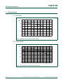
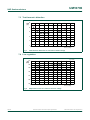
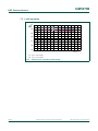
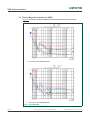
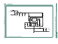
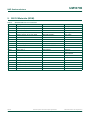
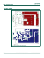
UM10796 SSL5031CDB1210 18 W universal non-isolated buck LED driver demo board Rev. 1.1 — 17 December 2014 User manual Document information Info Content Keywords SSL5031CDB1210, buck, universal input, fixture application Abstract This user manual describes the performance, technical data, and the connection of the SSL5031CDB1210 demo board, using non-isolated buck topology. The SSL5031CTS is an NXP Semiconductors driver IC in TSOP6 package. It is intended to provide a low-cost, small form factor LED driver design. This SSL5031CDB1210 demo board is designed for fixture applications. It operates at a universal input range (90 V (AC)to 265 V (AC). The output voltage is approximately 53 V. UM10796 NXP Semiconductors SSL5031CDB1210 18 W universal non-isolated buck LED driver Revision history Rev Date Description v.1.1 20141217 updated issue v.1 20141027 first issue Contact information For more information, please visit: http://www.nxp.com For sales office addresses, please send an email to: [email protected] UM10796 User manual All information provided in this document is subject to legal disclaimers. Rev. 1.1 — 17 December 2014 © NXP Semiconductors N.V. 2014. All rights reserved. 2 of 18 UM10796 NXP Semiconductors SSL5031CDB1210 18 W universal non-isolated buck LED driver 1. Introduction WARNING Lethal voltage and fire ignition hazard The non-insulated high voltages that are present when operating this product, constitute a risk of electric shock, personal injury, death and/or ignition of fire. This product is intended for evaluation purposes only. It shall be operated in a designated test area by personnel qualified according to local requirements and labor laws to work with non-insulated mains voltages and high-voltage circuits. This product shall never be operated unattended. This user manual describes the operation of the SSL5031CDB1210 demo board featuring the Solid-State-Lighting (SSL) LED driver SSL5031CTS in a universal input/18 W non-isolated application. The SSL5031CDB1210 demo board is designed for driving LED loads from 35 V to 60 V. The nominal load is 53 V. The PCB dimensions are compatible with fixture application. The SSL5031CDB1210 demo board provides a simple and effective solution with a high Power Factor (PF), low Total Harmonic Distortion (THD), and high efficiency for Solid-State Lighting (SSL) applications. 1.1 Features • • • • • • • • Compact design with a low component count High efficiency: 90.3 % at 120 V (AC) and 88.7 % at 230 V (AC) Excellent line and load regulation Power factor > 0.9; A-THD: < 17.2 % at 120 V (AC) and < 20.8 % at 230 V (AC) Fixture applications Open LED string protection/short LED string protection Compliant with EN55015 conducted EMI Compliant with 2.5 kV ring wave and 2 kV combination wave line surge Figure 3 shows the assembled top and bottom views. UM10796 User manual All information provided in this document is subject to legal disclaimers. Rev. 1.1 — 17 December 2014 © NXP Semiconductors N.V. 2014. All rights reserved. 3 of 18 UM10796 NXP Semiconductors SSL5031CDB1210 18 W universal non-isolated buck LED driver 2. Safety warning The demo board input is connected to the 90 V to 265 V (AC) mains. Avoid touching the board while it is connected to the mains voltage and when it is in operation. An isolated housing is obligatory when used in uncontrolled, non-laboratory environments. Galvanic isolation from the mains phase using a fixed or variable transformer is always recommended. Figure 1 shows the symbols on how to recognize these devices. 019aab174 019aab173 a. Isolated Fig 1. UM10796 User manual b. Not isolated Isolation symbols All information provided in this document is subject to legal disclaimers. Rev. 1.1 — 17 December 2014 © NXP Semiconductors N.V. 2014. All rights reserved. 4 of 18 UM10796 NXP Semiconductors SSL5031CDB1210 18 W universal non-isolated buck LED driver 3. Specifications Table 1 lists the specification of the SSL5031CDB1210 demo board. Table 1. SSL5031CDB1210 specifications Symbol Parameter Value Vmains AC mains supply voltage 90 V to 265 V (AC) Pout output power 15.9 W VLED output voltage 35 V to 60 V (53 V nominal) ILED output current 300 mA Iripple output current ripple 42 % (peak-to-peak) ILED/Vmains line regulation 0.057 mA/V; 1.7 % ILED/VLED load regulation 0.16 mA/V; 0.3 % at 10 % VLED efficiency 90.3 % at 120 V (AC)/60 Hz 88.7 % at 230 V (AC)/50 Hz PF power factor 0.98 at 120 V (AC)/60 Hz 0.95 at 230 V (AC)/50 Hz THD total harmonic distortion 17.2 % at 120 V (AC)/60 Hz 20.8 % at 230 V (AC)/50 Hz Toper operating temperature 40 C to +50 C - board dimensions 49 mm 28 mm - conducted electrostatic Interference (EMI) EN55015 Figure 2 shows the dimensions of the demo board. Fig 2. UM10796 User manual SSL5031CDB1210 demo board dimensions All information provided in this document is subject to legal disclaimers. Rev. 1.1 — 17 December 2014 © NXP Semiconductors N.V. 2014. All rights reserved. 5 of 18 UM10796 NXP Semiconductors SSL5031CDB1210 18 W universal non-isolated buck LED driver 4. Board photographs a. Top view b. Bottom view Fig 3. UM10796 User manual SSL5031CDB1210 demo board photographs All information provided in this document is subject to legal disclaimers. Rev. 1.1 — 17 December 2014 © NXP Semiconductors N.V. 2014. All rights reserved. 6 of 18 UM10796 NXP Semiconductors SSL5031CDB1210 18 W universal non-isolated buck LED driver 5. Board connections The SSL5031CDB1210 demo board is optimized for a 90 V to 265 V (AC) mains supply. It is designed to work with multiple LEDs or an LED module. Under the expected conditions, the output current is 300 mA when using an LED string with a forward voltage (VF) from 35 V to 60 V. The current can be adjusted using resistors R1 and R2. J1 and J2 are the connections for the mains voltage. J3 (LED+) and J4 (LED) are the connections for the LED load. Figure 4 shows the connections. Fig 4. UM10796 User manual SSL5031CDB1210 board connections All information provided in this document is subject to legal disclaimers. Rev. 1.1 — 17 December 2014 © NXP Semiconductors N.V. 2014. All rights reserved. 7 of 18 UM10796 NXP Semiconductors SSL5031CDB1210 18 W universal non-isolated buck LED driver 6. Functional description 6.1 Input filtering Capacitors C1 and C2 and inductor L1 filter the switching current from the buck converter to the line. Capacitors C1 and C2 also provide a low-impedance path for the switching current. To retain a power factor > 0.9, the value of capacitors C1 and C2 must be kept low. Varistor MOV1 across the AC line and the Transient Voltage Suppressor (TVS) diode on Vbus provide protection against transient surge voltages. 6.2 Setting the output current The LED output current is the primary parameter to set in an LED driver. It is regulated and sensed using Rsense resistors R1 and R2. The LED output current can be calculated with Equation 1: V reg AV ISNS I LED = ----------------------------R sense (1) Where: • Vreg(AV)ISNS = 0.4 V V ISNS max Remark: I peak max = ------------------------- determines the maximum peak. R sense 6.3 Output OverVoltage Protection (OVP) Output OVP is implemented by measuring the voltage at the DEMOVP pin during the secondary stroke. The DEMOVP pin senses the output voltage through resistive divider (R5, R6, and R7) connected between the LEDP node and the DEMOVP pin. When it reaches V(th)ovp in an open-load condition, OVP is triggered and IC restarts when the VCC voltage is discharged internally. To prevent false OVP detection, an internal counter ensures that the OVP level is reached in three continuous cycles, triggering the OVP protection. So, to dissipate the energy from those three cycles during every restart, an output resistor (R8) is required. Remark: In SSL5031BTS version, DEMOVP pin is also used for thermal foldback protection. For more information, see the SSL5031BTS data sheet. UM10796 User manual All information provided in this document is subject to legal disclaimers. Rev. 1.1 — 17 December 2014 © NXP Semiconductors N.V. 2014. All rights reserved. 8 of 18 UM10796 NXP Semiconductors SSL5031CDB1210 18 W universal non-isolated buck LED driver 7. Performance 7.1 Efficiency DDD Ș Fig 5. 9PDLQV9$& Efficiency as a function of mains voltage 7.2 Power factor DDD 3) Fig 6. UM10796 User manual 9PDLQV9$& Power factor as a function of mains voltage All information provided in this document is subject to legal disclaimers. Rev. 1.1 — 17 December 2014 © NXP Semiconductors N.V. 2014. All rights reserved. 9 of 18 UM10796 NXP Semiconductors SSL5031CDB1210 18 W universal non-isolated buck LED driver 7.3 Total harmonic distortion DDD 7+' Fig 7. 9PDLQV9$& Total harmonic distortion as a function of mains voltage 7.4 Line regulation DDD ,/(' P$ Fig 8. UM10796 User manual 9PDLQV9$& Output LED current as a function of mains voltage All information provided in this document is subject to legal disclaimers. Rev. 1.1 — 17 December 2014 © NXP Semiconductors N.V. 2014. All rights reserved. 10 of 18 UM10796 NXP Semiconductors SSL5031CDB1210 18 W universal non-isolated buck LED driver 7.5 Load regulation DDD ,/(' P$ 9/('9 (1) Vmains = 230 V (AC) (2) Vmains = 120 V (AC) Fig 9. UM10796 User manual LED current as a function of LED voltage All information provided in this document is subject to legal disclaimers. Rev. 1.1 — 17 December 2014 © NXP Semiconductors N.V. 2014. All rights reserved. 11 of 18 UM10796 NXP Semiconductors SSL5031CDB1210 18 W universal non-isolated buck LED driver 7.6 ElectroMagnetic Interference (EMI) Figure 11 shows the conducted EMI result of the SSL5031CDB1210 demo board. a. 120 V/60 Hz and EN55015B limits b. 230 V/50 Hz and EN55015B limits Fig 10. Conducted EMI UM10796 User manual All information provided in this document is subject to legal disclaimers. Rev. 1.1 — 17 December 2014 © NXP Semiconductors N.V. 2014. All rights reserved. 12 of 18 xxxxxxxxxxxxxxxxxxxxx xxxxxxxxxxxxxxxxxxxxxxxxxx xxxxxxx x x x xxxxxxxxxxxxxxxxxxxxxxxxxxxxxx xxxxxxxxxxxxxxxxxxx xx xx xxxxx xxxxxxxxxxxxxxxxxxxxxxxxxxx xxxxxxxxxxxxxxxxxxx xxxxxx xxxxxxxxxxxxxxxxxxxxxxxxxxxxxxxxxxx xxxxxxxxxxxx x x xxxxxxxxxxxxxxxxxxxxx xxxxxxxxxxxxxxxxxxxxxxxxxxxxxx xxxxx xxxxxxxxxxxxxxxxxxxxxxxxxxxxxxxxxxxxxxxxxxxxxxxxxx xxxxxxxx xxxxxxxxxxxxxxxxxxxxxxxxx xxxxxxxxxxxxxxxxxxxx xxx NXP Semiconductors UM10796 User manual 8. Schematic ) - 567 9$& 029 (5=9' - %' %6* / P+ & Q) 9 5 Nȍ ' 60$-&$ 5 Nȍ 4 $2,1 8 ,616 9&& 6: 5 Nȍ 5 Nȍ 66/&7 & QP &203 *1' '(0293 5 ȍ 5 Nȍ 5 ȍ & Q) 9 / + & ) 9 *1' - 5 Nȍ & ) 9 9 P$ - DDD Fig 11. SSL5031CDB1210 demo board schematic UM10796 13 of 18 © NXP Semiconductors N.V. 2014. All rights reserved. ' (6 SSL5031CDB1210 18 W universal non-isolated buck LED driver Rev. 1.1 — 17 December 2014 All information provided in this document is subject to legal disclaimers. & Q) 9 UM10796 NXP Semiconductors SSL5031CDB1210 18 W universal non-isolated buck LED driver 9. Bill Of Materials (BOM) Table 2. SSL5031CDB1210 bill of materials Reference Description and values Part number Manufacturer BD1 bridge rectifier; 1000 V; 0.8 A B10S-G Comchip Tech C1 capacitor; 0.1 F; 450 V ECW-F2W104JAQ Panasonic C2 capacitor; 0.22 F; 450 V ECW-F2W224JAQ Panasonic C3 capacitor; 1 F; 50 V; X7R; 0805 CL21B105KBFNNNE Samsung C4 capacitor; 220 nF; 50 V; X7R; 0603 UMK212B7224KG-T Taiyo Yuden C5 capacitor; 390 F; 63 V EKZE630ELL391MK25S Chemi-Con D1 diode; fast; 600 V; 2 A ES2J-LTP Micro Commercial D2 diode; TVS; 400 V SMAJ400CA Littelfuse F1 fuse; 250 V (AC) RST 3.15 Bel Fuse L1 inductor; 3300 H RL‐5480HC‐3‐3300 Renco L2 inductor, 680 H MSS1210-684KEB Coilcraft MOV1 varistor; 387 V ERZ-V10D431 Panasonic Q1 N-MOSFET; 650 V; 7 A AOI7N65 Alpha & Omega Semiconductor R1 resistor; 1.5 ; 1206; 1 % CRCW12061R50FKEA Vishay R2 resistor; 14 W; 1206, 1 % ERJ-8ENF14R0V Panasonic R3; R4 resistor; 105 k, 1206; 1 % ERJ-8ENF1053V Panasonic R5; R6 resistor; 78.7 k; 1206; 1 % ERJ-8ENF7872V Panasonic R7 resistor, 4.53 k; 0603; 1 % ERJ-3EKF4531V Panasonic R8 resistor; 40.2 k; 0805 RMCF0805FT40K2 Stackpole Electronics U1 IC; SSL5031CTS; TSOP6 SSL5031CTS NXP Semiconductors UM10796 User manual All information provided in this document is subject to legal disclaimers. Rev. 1.1 — 17 December 2014 © NXP Semiconductors N.V. 2014. All rights reserved. 14 of 18 UM10796 NXP Semiconductors SSL5031CDB1210 18 W universal non-isolated buck LED driver 10. Board layout a. Top view b. Bottom view Fig 12. SSL5031CDB1210 demo board layout UM10796 User manual All information provided in this document is subject to legal disclaimers. Rev. 1.1 — 17 December 2014 © NXP Semiconductors N.V. 2014. All rights reserved. 15 of 18 UM10796 NXP Semiconductors SSL5031CDB1210 18 W universal non-isolated buck LED driver 11. Abbreviations Table 3. Abbreviations Acronym Description EMI ElectroMagnetic Interference LED Light-Emitting Diode OCP OverCurrent Protection OTP OverTemperature Protection PF Power Factor SSL Solid-State Lighting 12. References [1] UM10796 User manual SSL5031CTS data sheet — Compact high power factor/low-THD buck LED driver IC All information provided in this document is subject to legal disclaimers. Rev. 1.1 — 17 December 2014 © NXP Semiconductors N.V. 2014. All rights reserved. 16 of 18 UM10796 NXP Semiconductors SSL5031CDB1210 18 W universal non-isolated buck LED driver 13. Legal information 13.1 Definitions Draft — The document is a draft version only. The content is still under internal review and subject to formal approval, which may result in modifications or additions. NXP Semiconductors does not give any representations or warranties as to the accuracy or completeness of information included herein and shall have no liability for the consequences of use of such information. NXP Semiconductors does not accept any liability related to any default, damage, costs or problem which is based on any weakness or default in the customer’s applications or products, or the application or use by customer’s third party customer(s). Customer is responsible for doing all necessary testing for the customer’s applications and products using NXP Semiconductors products in order to avoid a default of the applications and the products or of the application or use by customer’s third party customer(s). NXP does not accept any liability in this respect. Export control — This document as well as the item(s) described herein may be subject to export control regulations. Export might require a prior authorization from competent authorities. 13.2 Disclaimers Limited warranty and liability — Information in this document is believed to be accurate and reliable. However, NXP Semiconductors does not give any representations or warranties, expressed or implied, as to the accuracy or completeness of such information and shall have no liability for the consequences of use of such information. NXP Semiconductors takes no responsibility for the content in this document if provided by an information source outside of NXP Semiconductors. In no event shall NXP Semiconductors be liable for any indirect, incidental, punitive, special or consequential damages (including - without limitation - lost profits, lost savings, business interruption, costs related to the removal or replacement of any products or rework charges) whether or not such damages are based on tort (including negligence), warranty, breach of contract or any other legal theory. Notwithstanding any damages that customer might incur for any reason whatsoever, NXP Semiconductors’ aggregate and cumulative liability towards customer for the products described herein shall be limited in accordance with the Terms and conditions of commercial sale of NXP Semiconductors. Right to make changes — NXP Semiconductors reserves the right to make changes to information published in this document, including without limitation specifications and product descriptions, at any time and without notice. This document supersedes and replaces all information supplied prior to the publication hereof. Suitability for use — NXP Semiconductors products are not designed, authorized or warranted to be suitable for use in life support, life-critical or safety-critical systems or equipment, nor in applications where failure or malfunction of an NXP Semiconductors product can reasonably be expected to result in personal injury, death or severe property or environmental damage. NXP Semiconductors and its suppliers accept no liability for inclusion and/or use of NXP Semiconductors products in such equipment or applications and therefore such inclusion and/or use is at the customer’s own risk. Applications — Applications that are described herein for any of these products are for illustrative purposes only. NXP Semiconductors makes no representation or warranty that such applications will be suitable for the specified use without further testing or modification. Customers are responsible for the design and operation of their applications and products using NXP Semiconductors products, and NXP Semiconductors accepts no liability for any assistance with applications or customer product design. It is customer’s sole responsibility to determine whether the NXP Semiconductors product is suitable and fit for the customer’s applications and products planned, as well as for the planned application and use of customer’s third party customer(s). Customers should provide appropriate design and operating safeguards to minimize the risks associated with their applications and products. Evaluation products — This product is provided on an “as is” and “with all faults” basis for evaluation purposes only. NXP Semiconductors, its affiliates and their suppliers expressly disclaim all warranties, whether express, implied or statutory, including but not limited to the implied warranties of non-infringement, merchantability and fitness for a particular purpose. The entire risk as to the quality, or arising out of the use or performance, of this product remains with customer. In no event shall NXP Semiconductors, its affiliates or their suppliers be liable to customer for any special, indirect, consequential, punitive or incidental damages (including without limitation damages for loss of business, business interruption, loss of use, loss of data or information, and the like) arising out the use of or inability to use the product, whether or not based on tort (including negligence), strict liability, breach of contract, breach of warranty or any other theory, even if advised of the possibility of such damages. Notwithstanding any damages that customer might incur for any reason whatsoever (including without limitation, all damages referenced above and all direct or general damages), the entire liability of NXP Semiconductors, its affiliates and their suppliers and customer’s exclusive remedy for all of the foregoing shall be limited to actual damages incurred by customer based on reasonable reliance up to the greater of the amount actually paid by customer for the product or five dollars (US$5.00). The foregoing limitations, exclusions and disclaimers shall apply to the maximum extent permitted by applicable law, even if any remedy fails of its essential purpose. Safety of high-voltage evaluation products — The non-insulated high voltages that are present when operating this product, constitute a risk of electric shock, personal injury, death and/or ignition of fire. This product is intended for evaluation purposes only. It shall be operated in a designated test area by personnel that is qualified according to local requirements and labor laws to work with non-insulated mains voltages and high-voltage circuits. The product does not comply with IEC 60950 based national or regional safety standards. NXP Semiconductors does not accept any liability for damages incurred due to inappropriate use of this product or related to non-insulated high voltages. Any use of this product is at customer’s own risk and liability. The customer shall fully indemnify and hold harmless NXP Semiconductors from any liability, damages and claims resulting from the use of the product. Translations — A non-English (translated) version of a document is for reference only. The English version shall prevail in case of any discrepancy between the translated and English versions. 13.3 Trademarks Notice: All referenced brands, product names, service names and trademarks are the property of their respective owners. GreenChip — is a trademark of NXP Semiconductors N.V. UM10796 User manual All information provided in this document is subject to legal disclaimers. Rev. 1.1 — 17 December 2014 © NXP Semiconductors N.V. 2014. All rights reserved. 17 of 18 UM10796 NXP Semiconductors SSL5031CDB1210 18 W universal non-isolated buck LED driver 14. Contents 1 1.1 2 3 4 5 6 6.1 6.2 6.3 7 7.1 7.2 7.3 7.4 7.5 7.6 8 9 10 11 12 13 13.1 13.2 13.3 14 Introduction . . . . . . . . . . . . . . . . . . . . . . . . . . . . 3 Features . . . . . . . . . . . . . . . . . . . . . . . . . . . . . . 3 Safety warning . . . . . . . . . . . . . . . . . . . . . . . . . . 4 Specifications. . . . . . . . . . . . . . . . . . . . . . . . . . . 5 Board photographs . . . . . . . . . . . . . . . . . . . . . . 6 Board connections . . . . . . . . . . . . . . . . . . . . . . 7 Functional description . . . . . . . . . . . . . . . . . . . 8 Input filtering . . . . . . . . . . . . . . . . . . . . . . . . . . . 8 Setting the output current . . . . . . . . . . . . . . . . . 8 Output OverVoltage Protection (OVP) . . . . . . . 8 Performance . . . . . . . . . . . . . . . . . . . . . . . . . . . . 9 Efficiency . . . . . . . . . . . . . . . . . . . . . . . . . . . . . 9 Power factor . . . . . . . . . . . . . . . . . . . . . . . . . . . 9 Total harmonic distortion. . . . . . . . . . . . . . . . . 10 Line regulation . . . . . . . . . . . . . . . . . . . . . . . . 10 Load regulation . . . . . . . . . . . . . . . . . . . . . . . . 11 ElectroMagnetic Interference (EMI) . . . . . . . . 12 Schematic . . . . . . . . . . . . . . . . . . . . . . . . . . . . . 13 Bill Of Materials (BOM) . . . . . . . . . . . . . . . . . . 14 Board layout . . . . . . . . . . . . . . . . . . . . . . . . . . . 15 Abbreviations . . . . . . . . . . . . . . . . . . . . . . . . . . 16 References . . . . . . . . . . . . . . . . . . . . . . . . . . . . 16 Legal information. . . . . . . . . . . . . . . . . . . . . . . 17 Definitions . . . . . . . . . . . . . . . . . . . . . . . . . . . . 17 Disclaimers . . . . . . . . . . . . . . . . . . . . . . . . . . . 17 Trademarks. . . . . . . . . . . . . . . . . . . . . . . . . . . 17 Contents . . . . . . . . . . . . . . . . . . . . . . . . . . . . . . 18 Please be aware that important notices concerning this document and the product(s) described herein, have been included in section ‘Legal information’. © NXP Semiconductors N.V. 2014. All rights reserved. For more information, please visit: http://www.nxp.com For sales office addresses, please send an email to: [email protected] Date of release: 17 December 2014 Document identifier: UM10796