1
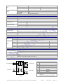
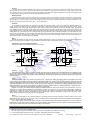
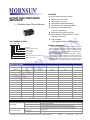
FEATURES
l 2-port isolation (input and output)
ACTIVE HIGH PRECISION
AMPLIFIER
——Detection type TExxxxN series
l
l
l
l
l
High accuracy (0.1% F.S.)
High linearity (0.1% F.S.)
High isolation voltage(2KVAC/60s)
Low ripple & noise: ≤30mVpp (20MHz)
Extremely low temperature drift
(-25~+71℃:≤35PPM/℃)
l Small size: DIP18 (26*9.5*12.5mm)
l ESD protection (IEC/EN61000-4-2 contact
±4KV perf. Criteria B)
l With load ability:
≥2KΩ (@MAX SIGNAL OUTPUT @10V)
PART NUMBER SYSTEM
TEXXXXN
GENERAL DESCRIPTION
Package
Isolation power output
Power supply
Signal output
Signal input
Double isolation detection type
Isolation amplifier
The TExxxxN series is with preceding voltage/current signal
input and backward voltage signal output, and with an inner high
efficiency isolated micro-power source. It can provide isolation
power to peripheral circuit at the same time of providing power to
internal signal processing circuit.
Adopting electromagnetism isolation technology, therefore
compared with photo-coupler isolation, it has higher accuracy and
lower temperature drift. This module is two-port isolation (input
and output). There are external functions for the series as zeros
and full adjustment, convenient for customer to design and adjust.
SELECTION GUIDE
Model
Power Supply
Input
Output
TE5534N
24V
0~10V
0~10V
Isolation Power Output
15V
Channels
1
TE5544N
15V
0~10V
0~10V
15V
1
TE5554N
12V
0~10V
0~10V
15V
1
TE5634N
24V
0~10V
0~5V
15V
1
TE6634N
24V
0~5V
0~5V
15V
1
TE6644N
15V
0~5V
0~5V
15V
1
TE6654N
12V
0~5V
0~5V
15V
1
TE6664N
5V
0~5V
0~5V
15V
1
TE1433N
24V
4~20mA
1-5V
24V
1
TE1533N
24V
4~20mA
0~10V
24V
1
TE1530N
24V
4~20mA
0~10V
NONE
1
TE1550N
12V
4~20mA
0~10V
NONE
1
TE1633N
24V
4~20mA
0~5V
24V
1
TE1630N
24V
4~20mA
0~5V
NONE
1
TE1660N
5V
4~20mA
0~5V
NONE
1
ELECTRICAL SPECIFICATIONS
Power Supply
Isolation Power Output
Power Supply
(Nominal power supply)±5%
Input Power
≤1.0W(No isolation power output) ≤1.5W(No isolation power output)
Power Protection
Reverse protection(The product of 5V power input is without this function )
Output Voltage
(Nominal)±10%
Output Current
≤25mA
The copyright and authority for the interpretation of the products are reserved by MORNSUN
TExxxxN
2013.07.25-wip
Page 1 of 6
Input
Output
Input Signal
Refer to the above selection guide
Input Impedance
≥10MΩ(Max. voltage signal input) ≤250mV(Max. current signal input)
Over-load
≤30V(Voltage signal input)
Output Signal
Refer to the above selection guide
With Load Ability
≥2kΩ
Ripple & Noise
≤30mVpp(20MHz bandwidth)
≤50mA(Current signal input)
TRANSMISSION SPECIFICATIONS
Zero Offset
0.1%F.S.
Accuracy
0.1%F.S.
Temperature Drift
35PPM/℃(-25~+71℃); 50PPM/℃(-40~+85℃)
Adjustable Function
Full Degree Regulation
Can be adjusted within ±5% output signal range
Zero Regulation
Can be adjusted within ±5% output signal range
Bandwidth
≥2KHz
Response Time
≤1mS
Frequency Response
ISOLATION SPECIFICATIONS
Power input and the signal output are on the common ground. Power output and the signal input are on the common ground.
Electrical Isolation
Isolated between power input and the signal output or power input and power distribution output.
Isolation voltage
2.0KVAC(Tested for 1minute, leakage current<1mA, humidity <70%)
Insulation Resistance
100MΩ(500VDC)
EMC SPECIFICATIONS
EMI
EMS
CE
CISPR22/EN55022
CLASS A (Recommended Circuit Refer to Figure 1)
RE
CISPR22/EN55022
CLASS A
ESD
IEC/EN61000-4-2
Contact ±4KV
perf. Criteria B
RS
IEC/EN61000-4-3
10V/m
perf. Criteria A
EFT
IEC/EN61000-4-4
Power port ±2KV (Recommended Circuit Refer to Figure 1)
perf. Criteria B
Surge
IEC/EN61000-4-5
Power port ±1KV/±2KV (Recommended Circuit Refer to Figure 1)
perf. Criteria B
CS
IEC/EN61000-4-6
3 Vr.m.s
perf. CriteriaA
OTHER SPECIFICATIONS
Operating temperature:- 40~+85℃
Ambient Temperature
Transport and storage temperature: -50~+105℃
Package
DIP18
Weight
8g (typ.)
Application Environment
Dust-free, fierce shocking, impulsion and corrosive gas
APPLICATION CIRCUIT DIAGRAM
Power distributionC1
10 +
18+
D1
D2
11 −
17 −
16
15
9+
Signal input
C2
R1
Power
supply
supply
Power
R5
R2
1+
D3
D4
8−
Signal output
2−
R3
R4
3
C1
C2
R1
100uF/35V
100uF/35V
①
Negative zero adjustment resistance
R2
Positive zero adjustment resistance
①
①
R3
Positive gain adjustment resistance
R4
Negative gain adjustment resistance
R5
D1
D2
D3
D4
Positive zero adjustment resistance
SMCJ30A
SMCJ28A
SMBJ15A
SMBJ15A
①
①②
Note: ① Adjustment resistance is choosed according to the
requirement.
② R5 is only used for regulation of 24V input product.
(Figure 1)
The copyright and authority for the interpretation of the products are reserved by MORNSUN
TExxxxN
2013.07.25-wip
Page 2 of 6
APPLICATION
1.Schematic diagram
ISO Power
Out
ISO Power
Power
in
Power In
OSC
AMP
Signal
In
MOD
DEMOD
Offset Trim
AMP
Signal
Out
Gain Trim
2.Typical application——Multi-channel signal acquisition
Application circuit for typical multi-channel signal acquisition is as below:
ISOVCC
VCC
A0
ISOVCC
VCC
ISOVCC
A1
VCC
Sin1
X0
A0
Y0
A1
ISOVCC
VCC
Pin+
Pout+
X1
Sin2
Y1
4052
X2
Sin3
Sout+
Sin+
X
Sout-/ Pin-
Sin-/ Pout-
Y
Signal out
Y2
X3
Sin4
TE - N 双隔离变送器
TE_N amplifier
INHIBIT
Y3
VSS
VEE
Multi-channel signal acquisition application circuit
Function
In the figure,Sin1~Sin4 are external input signal,A0~A1 are strobe signal, and signal out is an external input signal of control system to accept.
The optocoupler in the circuit implements the isolated transmission of strobe signals. Amplifier of TE-N series implem ents the isolated
transmission of signals and isolated power supplement. The multi-channel strobe chips 4052 implements selective transmission of multiplex
signals.
Working principle
When the circuit works, the control system sends out the strobe signal A0~A1. Optical coupling isolation circuit transfers strobe signal to
multi-channel strobe chips 4052, and control the chip to correspond channel. External signal Sin1~Sin4 input to multi-channel strobe chips 4052.
After a chip strobe, strobe signal transfers to the signal input of TE _ N transmitter. TE_ N transmitter output the isolated input signal to control
system, thus it implements the control system and the external signal isolation circuit. Input power of TE_N transmitter and the input Vcc of strobe
signal transmission circuit are provided by control system. After strobe signal is isolated, transmission circuit power and multi-channel strobe chips
4052 power supply ISOVCC are provided by power distribution output Pout+.
3.Typical application ——Isolated transmission for electrical signals
Typical application of isolated transmission for electrical signals is below.
Pin+
Pout+
VCC
R1
Sout+
Sin+
Signal in
R4
R2
431
Sin-/ Pout-
Signal out
C1 R5
Sout-/ Pin-
R3
10V
10V
5V
5V
5V
-5V
Isolated transmission for electrical signals application
The copyright and authority for the interpretation of the products are reserved by MORNSUN
TExxxxN
2013.07.25-wip
Page 3 of 6
Function
In the figure, Signal in is detected electrical signals, Signal out is electrical signals for control system of isolation transmission. VCC is isolated power
supply provided from control system. Typical power signal is positive and negative sine wave signal. 431 R1 R2 and R3 is voltage stabilizing circuit in the
circuit, and they can achieve zero adjustment of the input signal. Amplifier of TE_N series achieve signal transmission function and power supply function
of voltage stabilizing circuit. R4,R5,C1 achieve DC output signal filtering functions.
Working principle
Supposing detected signal is 5V sine wave signal. When the input signal is passed through stabilizing circuit which is composed of 431,R1,R2 and R3,
input signal of TE_N transmitter become 0~10V sine wave signal. If the amplifier is the one which has 0~10V input and 0~10V output, TE_N transmitter output
would be output 0~10 v sine wave signal at this time. After passed through filter circuit which is composed of R4,R5 and C1, the DC component of 0~10V
sine wave signal is filtered, and the output only have ±5V sine wave signal.
Parameter
In the application, typical values of R1, R2 and R3 are 10KΩ, and reference Voltage of 413 is 2.5V. Component regulated voltage is 5V.
Voltage accuracy can achieve a variety of application requirements of high precision according to the resistance tolerance precision. Typical
application range of R4 is 2KΩ~5KΩ. Because signal output voltage is positive and negative, there will be a transmitter output signal current
return-irrigation phenomenon when the voltage signal output is negative.R4 should choose a smaller value in order to reduce the influence of the
return-irrigation current. C1 should be chosen low internal resistance capacitance. Normally ceramic capacitor with volume more than 10uF will be
suitable. Because C1 achieves the function of getting through AC and preventing DC. Large capacitance resistance and small capacitance value
can make AC signal distorted. The recommended value of R5 should be more than 100KΩ, and implem ents a DC signal to zero in the circuit. The
increase of value of R5 can make the time of DC signal to zero longer, and make the startup time longer. If load in circuit is too small, then the load
for AC will be increased, so that AC signal will be distorted.
Notice
Because the transmitter of TE_N series can not input negative voltage signal, it need to pay attention to narrow signal voltage amplitude and
have the necessary margin in the design. It can guarantee the normal work of the circuit and reduce the risk of signal distortion.
4.Application—Zero and full adjustment function
Zero and full adjustment recommended setting circuit is as shown
C1
10 +
18 +
D1
D2
11 −
17 −
Power distribution
output
9+
D5
8−
C1
Power input
16
Zero adjustment
Power distribution
potentiometer
output
Power output
Full adjustment
3
Power input
Zero adjustment
16
9+
2−
Singal input
17 −
potentiometer
1+
D4
C2
D2
D1
11−
15
D3
18 +
10 +
C2
D3
D5
1+
D4
8−
2−
Singal input
3
potentiometer
Routine zero and full adjustment circuit
Power output
Full adjustment
potentiometer
24 V power input zero and full adjustment circuit
Function
Zero adjustment function by setting up adjustment resistor at the zero point can change the zero signal transmission, which makes the output
signal overall migration. Full adjustment function is also called the gain adjustment function, and it can change the ratio of signal transmission
through the set up corresponding adjust resistance at the full adjustment, and the isolation transmission proportion of input and output signal value
would be changed.
Usage
Adding and reducing negative zero resistance can reduce the zero of signal output. Adding and reducing positive zero resistance can increase
the zero of signal output. Adding and reducing negative full adjustable resistance can reduce the ratio of signal transmission, Adding and reducing
negative full adjustable resistance can increase the ratio of signal transmission. You can use potentiometer to adjust the output signal of zero and
full in practical application. As shown in the figure, the terminal of full or zero adjustment is connected to the sliding of potentiometer, and the both
ends of potentiom eter is to the zero or full reference of positive and negative regulating reference . Sliding potentiometer to adjust signal full or
changing the ratio of rise and fall can also adjust zero and full of the output signal.
As shown in the figure, zero positive reference adjusting is different between 24V input product and other power input products, so the zero
adjustment circuit is also different. Adjusting the potentiometer to positive can increase zero or full of the corresponding signal. Adjusting the
potentiometer to negative can reduce zero or full of the corresponding signal. The maximum recommended range of potentiometer is 10KΩ~1MΩ,
detail resistance selection according to the adjustment accuracy. Choose larger resistance potentiometer for high precision fine-tuning. Choose
smaller resistance potentiometer for a wide range of rough adjustment.
Notice
The accuracy of transmitter of TE_N series is already 0.1%FS during production and before shipment, using the function of zero and full
adjustment will affect original accuracy. Due to the effect on temperature drift of external adjustment resistor and the stability of the potentiometer,
temperature drift of product will be changed, too.
The 1:1 ratio for positive resistance and negative resistance of full adjustment potentiometer is desired full adjustment. For the zero adjustment
potentiometer, the ratio between positive resistance and negative resistance, which makes the zero point of different products predetermined Zero
point is diverse. Please set the value of potentiometer according to actual situation.
NOTICE
1.
2.
3.
4.
Please read the user manual carefully before using. If any question please contact our FAE.
Please do not use this product in hazardous area.
The power supply of this product should be 24VDC power source. It is forbidden to use 220VAC power supply.
To avoid invalid explosion protection function, or any failure, disassembling this product is forbidden.
The copyright and authority for the interpretation of the products are reserved by MORNSUN
TExxxxN
2013.07.25-wip
Page 4 of 6
AFTER-SALES SERVICE
1. Products are carefully inspected and quality controlled during production and before shipment. If they operated abnormally or there was anything
wrong, please contact our agent from which you purchased or MORNSUN FAE as soon as possible.
2. MORNSUN warranty our product for 3 years from manufacturing date. During this period, MORNSUN will repair or replace the product if product
was found to have manufacturing defect.
APPLICATION CIRCUIT
Please check “ A APPLICATION GUIDE TO ISOLATION TRANSMITTER”
DIMENSIONS, RECOMMENDED FOOTPRINT & PACKAGING
Note:
1. All specifications measured at Ta=25°C, humidity<75%, nominal input voltage and rated output load unless otherwise specified.
2. In this datasheet, all the test setup and methods are based on our corporate standards.
3. All characteristics are for listed models, and non-standard models may perform differently. Please contact our technical support for more details.
4. Contact us for your specific requirement.
5. Specifications of this product are subject to changes without prior notice.
MORNSUN Science & Technology Co.,Ltd.
Address: No. 5, Kehui St. 1, Kehui development center, Science Ave., Guangzhou Science City, Luogang district, Guangzhou,P.R.China.
Tel: 86-20-38601850
Fax:86-20-38601272
E-mail: [email protected]
Http://www.mornsun-power.com
The copyright and authority for the interpretation of the products are reserved by MORNSUN
TExxxxN
2013.07.25-wip
Page 5 of 6