1
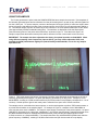
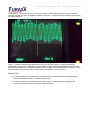
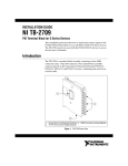
808 Gilman Street
Berkeley, CA., 94710
p:925.253.2960
www.furaxa.com
SAMPULSE50GHz and SAMPULSE70GHzANT
PULSER/SAMPLER DEMO BOARD
REV B. PRELIMINARY USER MANUAL
2/25/15
Figure 1. Connections to SAMPULSE50GHz (left) or SAMPULSE70GHzANT (right).
INTRODUCTION:
The SAMPULSE50GHz and SAMPULSE70GHzANT are demonstration boards for Furaxa InP single channel
sampler/pulser ICs. The SAMPULSE50GHz model contains a 2.4mm combined TDR input/output connector to
the common sampler/pulser node in the IC. The SAMPULSE70GHzANT is similar, except that instead of a
single-ended 2.4mm connector, the sampler IC’s differential inputs are fed from a bowtie antenna. In both
models, the IC's differential sampler output is converted, using an AD8009 op amp, into a single-ended groundreferenced output that is sent to an SMA jack labeled SAMPLER OUTPUT.
The sampler clock input is fed into the SMA jack labeled SAMPLER CLOCK, and should ideally be a square
wave with rise time under 150pS and amplitude of approximately 1V to 1.5V p-p. It may be set to any frequency
from 1 MHz to 3GHz (a +12dBm sine wave input with approximately a 50% duty cycle may be substituted for the
square wave for frequencies above 200MHz), causing the board take samples at rates from 1 million to 3 billion
per second. Amplitude of either sine or square wave sampler clock input should be approximately +12dBm
(~850mV RMS). The module is calibrated at the factory using a 1GHz sampler clock frequency. If
changing sampler frequency outside the 1GSPS to 2GSPS range, it will be necessary to readjust
potentiometer SVG3 as shown in Figure 2.
An optional pulser clock input is fed into the SMA jack labeled PULSER CLOCK IN, and may be set to any
frequency from 1 MHz to 3GHz. It should ideally be a 1V p-p square wave with rise time under 150pS and duty
cycle of approximately 50% (a +6dBm to +12dBm sine wave input may be substituted for the square wave for
frequencies above 200MHz). Each PCLK transition causes the board to produce a pulse on the sampler/pulser
node, which then appears at the 2.4mm sampler/pulser TDR input/output connector where it can be used to
stimulate an external device-under-test (DUT), while the board’s sampler can concurrently view this pulse and its
reflections, as well as any additional signal emitted from the external DUT. When the pulser is not used, the
board’s negative power supply should be reduced to -5V (from its default value of -7V) so as not to
couple in any noise that is generated by the pulser in the absence of a valid pulser clock.
808 Gilman Street
Berkeley, CA., 94710
p:925.253.2960
www.furaxa.com
SAMPLER SPECIFICATIONS:
Sample rate: 1MSPS to 3000MSPS (SVG3 must be adjusted for rates significantly different than 1GSPS)
Sampler clock input: AC-coupled, sine wave of amplitude +12dBm. Rise and fall times must be <150ps.
Sampler clock input waveshape: Sine wave of 200MHz to 3000MHz or Squarewave with frequency of 1MHz to
3GHz and risetime (10% to 80%) of 150ps or less. Duty cycle may be 40/60% to 60/40%
(50/50 preferred)
Number of channels: 1
Full Scale Input range: +/- 200mV – DO NOT EXCEED +/- 300mV or unit will be damaged.
3dB Input Bandwidth: 50 GHz for Sampulse50GHz model (70GHz for Sampulse70GHzAnt model)
6dB Input Bandwidth: 70 GHz for Sampulse50Ghz model
Usable Bandwidth while maintaining 50dB SNR: 70 GHz
Dynamic Range: 85dB typical, 2MHz to 50 GHz. Does not include coherent Fsample noise at output.
SFDR: Approximately 30dB at maximum input level. SVG3 and SVG2 may be adjusted to optimize SFDR.
Input connector type: 2.4MM Jack for Sampulse50GHz model, antenna for Sampulse70GHzAnt model
Clock input connector type: SMA Jack
Output connector type: SMA Jack
Output (IF) signal +/- 1V peak into 50 ohms (can produce up to +/-2.5V when sampler input is fed with
strong signal – Please note that some external circuitry may be damaged by these voltage levels).
IF output bandwidth: DC to 100MHz.
PULSER SPECIFICATIONS:
Pulser clock inputs: AC-coupled, amplitude 500mV p-p to 1200mV p-p.
Pulser clock input waveshape: Sine wave of 200MHz to 3000MHz or Squarewave with frequency of 1MHz to
3GHz and risetime (10% to 80%) of 150ps or less. Duty cycle may be 40/60% to 60/40%
(50/50 preferred)
Pulse repetition rate: 1MPPS to 2000MPPS (clock sources under 200MHz must be square wave with <150ps
rise time – slower rise times will result in broader, or nonexistent, output pulse and/or added jitter)
Pulse amplitude): Adjustable from approximately 30mV to 300mV. Pulser may be disabled by ensuring that
PCLK is not driven, and reducing negative power supply to -5V to prevent residual noise.
Pulse width, at 2.4mm input/output connector: Approximately 12ps, viewed on HP 54750/54752A scope,
approx. 7ps internal to IC when optimally adjusted using pot PVG3 and viewed directly by sampler on IC.
Demo Board Power Requirements:
+4.6V (may use +5V) at 80mA (typical), -5V at 150mA (typ.) when using sampler only (no pulser). Negative
supply must be set to -7V, and valid pulser clock applied, if using pulser.
Cooling Requirements:
Light Fan cooling recommended: 20LFPM minimum.
SETUP DIRECTIONS:
1) Verify that voltages on external power supply are set to +4.6V and -5V (-7V if using pulser). Turn off
external power supply, and connect both Orange and Red power input cable wires to grounds
(common) on external power supply. Connect +4.6 to +5V output to +5V wire on power cable.
Connect -5V (or -7V) output to wire labeled -5V(-7v if pulser). If not using pulser, then this wire
should instead be fed with -5V.
2) Using a high quality flexible 50 GHz microwave cable with 2.4MM connectors, connect the 2.4mm jack
to the desired RF signal source to be sampled or studied using the TDR capabilities of the
Sampulse50GHz. Board is fragile – do not apply excessive torque when tightening cables on
connectors on the SAMPULSE50GHz (a light finger tight connection is adequate on all cable
connections). 2.4MM CONNECTOR MUST NEVER BE CONNECTED TO ANY INPUT THAT
CONTAINS A VOLTAGE OF OVER +/-300mV, OR THE UNIT MAY BE DESTROYED - A FAILURE
NOT COVERED BY WARRANTY.
808 Gilman Street
Berkeley, CA., 94710
p:925.253.2960
www.furaxa.com
3) Using flexible cables, connect a square wave clock source of 500 – 1200mV p-p, with rise time <150ps,
to the SCLK (and optionally PCLK) connectors. For initial testing as a TDR, use a +12dBm sine wave or
square wave, with a frequency of 1000 MHz for PCLK and a frequency of 999.98MHz for SCLK. As the
output pulses are narrow (7ps) and may be difficult to find, it is most convenient to use as high a clock
frequency as possible for initial testing. If using SCLK frequencies significantly different than
1GHz, it will be necessary to readjust SVG3, and possibly SVG2 as shown in Figure 2. Similarly if
using PCLK frequencies significantly different than 1GHz, it will be necessary to readjust PVG3.
4) Connect the SMA SAMPLER OUTPUT signal to an oscilloscope, set for 10us per division, 50 ohm input
impedance and a vertical scale of 500mV or 1V per division.
5) Turn on the power supply and clock sources.
6) If you are using both the sampler and pulser, you should see a pulse with some ringing on the
oscilloscope, as shown in figure 4. Please refer to section “USING THE SAMPLER” for more details.
IMPORTANT: The samplers have been adjusted at the factory for optimal operation at
approximately 1GHz. When using significantly different sampling clock (SCLK) frequencies you
may need to adjust the SVG3 potentiometer (and possibly SVG2) slightly for optimal linearity and
bandwidth. For sampling rates significantly below 1GSPS, it may be necessary to adjust SVG3
for the sampler to function.
Figure 2. Adjusting sampling aperture for optimal bandwidth using SVG3 potentiometer. Necessary when
using SCLK frequencies significantly different than 1GHz.
808 Gilman Street
Berkeley, CA., 94710
p:925.253.2960
www.furaxa.com
USING THE SAMPLER.
The IC that generates the pulse inside the SAMPULSE50GHz has a sampler that can take ~7ps snapshots of
the internally generated pulse and its reflections from the device being driven, as well as any external signals fed
into the 2.4mm jack. To use the sampler, connect to the Sampler Clock Input (SCLK) a continuous square wave
having a frequency that differs from that of the continuous pulser clock (PCLK) input by approximately 20KHz or
so. The sampler output may then be viewed by an A/D converter or on a low-speed oscilloscope or ADC board
(with approximately 20 MHz bandwidth limiting filter). The waveform so displayed will be the heterodyned
(downconverted) picture of the pulse and its reflections, as shown in figure 3. Note that in this figure, the
sampler output shows the downconverted pulse and its reflection from the unconnected 2.4mm connector.
IMPORTANT: The sampler has been adjusted at the factory for optimal operation at 1000 MSPS. When
using different sampling clock frequencies (input to SCLK), you may need to adjust the SVG3, and
possibly the SVG2 potentiometer slightly for optimal linearity and bandwidth, or even for any sampler
operation at all.
Figure 3. TDR using sampler and pulser concurrently. Sampler output displayed shows heterodyne of train of
internally generated pulses spaced ~1ns apart (990 MPPS), generated by on-chip pulser. Sampler is run at
989.98 MSPS, resulting in 20,000 waveforms/second (50 microseconds of scope display corresponds to ~1ns of
real time). Smaller pulse to right of each main pulse is reflection from open end of 2.4mm connector.
The sampler can be used without the internal pulser, or can be used together to perform TDR measurements, or
to provide fiducial marks on the sampled signal. For example in Figure 4, a sampler clock of 989.98MHz is
used, and the pulser clock is 990MHz. The sampler output shows a heterodyne of the pulses spaced ~1ns apart
(990 MPPS), generated by on-chip pulser. Additionally, a 19.972GHz external signal is transmitted through air to
the attached bowtie antenna on A Sampulse70GHzAnt model (it may similarly be instead inputted via the
2.4GHz connector on a Sampulse50GHz). The sampler therefore runs at 989.98 MSPS (20KHz lower than the
pulser frequency of 990MHz), resulting in 20,000 waveforms/second (50 microseconds of scope display
808 Gilman Street
Berkeley, CA., 94710
p:925.253.2960
www.furaxa.com
corresponds to ~1ns of real time). As can be seen in Figure 4, approximately 20 cycles of the 19.972GHz
externally inputted sine wave are displayed between each of the ~1ns-separated pulses internally generated by
the sampler/pulser IC.
Figure 4. Sampler output showing heterodyne of pulse train of pulses spaced ~1ns apart (990 MPPS),
generated by on-chip pulser. Additionally, a superimposed 19.972GHz signal is transmitted through air to the
attached bowtie antenna on A Sampulse70GHzAnt model. Sampler is run at 989.98 MSPS, resulting in 20,000
waveforms/second (50 microseconds of scope display corresponds to ~1ns of real time).
KNOWN BUGS:
1) DC control voltages SVG3 (and sometimes SVG2) need to be readjusted when changing sampling
frequency outside the 1GSPS – 2GSPS frequency range.
2) DC control voltages PVG3 (and sometimes PVG2) need to be readjusted when changing pulse
repetition frequency from factory-calibrated 1GPPS frequency.