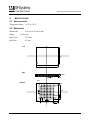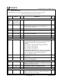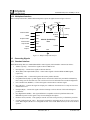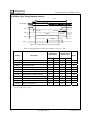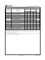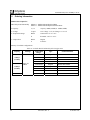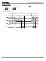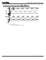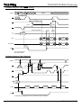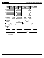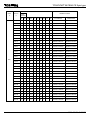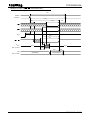
1
DiskOnChip-Based MCP with Mobile DiskOnChip Plus, CMOS (NOR) Flash, and PSRAM Data Sheet, Nov. 2003 Highlights DiskOnChip-based MCP (Multi-Chip Package) is a complete memory solution. Efficiently packed in a small Fine-Pitch Ball Grid Array (FBGA) package, it is ideal for data and code storage inside 2.5G and 3G mobile handsets and Personal Digital Assistants (PDAs). DiskOnChip-based MCP consists of: M-Systems’ Mobile DiskOnChip Toshiba’s CMOS (NOR) flash Toshiba’s PSRAM (Pseudo Static RAM) General Features Small 9x12x1.4 mm, 107-ball FBGA package 128Mbit (16MByte) Mobile DiskOnChip Plus 128Mbit (16MByte) Toshiba NOR flash 64Mbit (8MByte) Toshiba PSRAM High performance 16-bit interface to all devices Deep Power-Down mode for low power consumption Operating voltage: 2.7V to 3.3V Operating temperature: -30°C to +85°C 1 Mobile DiskOnChip Plus Mobile DiskOnChip Plus 128Mbit (16MByte) is the industry’s most efficient code and storage solution, with the fastest write performance, the smallest die size and the highest level of reliability and flash endurance. Additionally, Mobile DiskOnChip Plus offers advanced data protection and security-enabling options. Mobile DiskOnChip Plus features: Exceptional write, read, and erase performance Advanced protection and security-enabling features for data and code NAND-based flash technology that enables high density and small die size Proprietary TrueFFS technology for full hard disk emulation, high data integrity and maximum flash lifetime Programmable Boot Block with eXecute In Place (XIP) functionality using 16-bit access, with download support for more code to enable CPU initialization Platform initialization OS boot Data integrity with Reed-Solomon-based Error Detection Code/Error Correction Code (EDC/ECC) Data Sheet, Rev. 0.4 91-SR-001-53-8L DiskOnChip-Based MCP (MS01-D7N7P6-B1) Deep Power-Down mode for reduced power consumption Support for all major mobile operating systems (OSs), including Symbian OS Smartphone 2002/3 Pocket PC 2002/3 Windows CE/CE.NET Linux Nucleus Palm Easy-to-integrate configurable interface Simple SRAM-like interface Compatible with all major CPUs, including Texas Instruments OMAP Intel StrongARM/XScale Motorola MX1 Texas Instruments TMS320VC55x DSP NeoMagic MiMagic AMD Alchemy ARM-based CPUs Mode-control compatible with JEDEC standard commands Boot block architecture THPV067Z02BABD: top boot block THPV067Z03BABD: bottom boot block PSRAM Organization: 4M x 16 bits Power dissipation Operating: 50 mA max Standby: 100 µA max Deep Power-Down: 5 µA max Access time Random: 70 ns, CL = 30 pF Page: 30 ns, CL = 30 pF Modes Page read operation (8 words/page) Deep Power-Down NOR Flash Organization: 8M x 16 bits Power dissipation Read: 50 mA max Address increment read: 11 mA max Page read: 5 mA max Program/Erase: 15 mA max Standby: 10 µA max Access time Random: 65 ns, CL = 30 pF 70 ns, CL = 100 pF Page: 30 ns, CL = 30 pF 35 ns, CL = 100 pF Functions Simultaneous read/write Automatic operations: program, page program, chip erase, block erase Block erase architecture: 8x8KB/255x64KB Modes Fast program Acceleration 2 Data Sheet, Rev. 0.4 91-SR-001-53-8L DiskOnChip-Based MCP (MS01-D7N7P6-B1) REVISION HISTORY 1 Revision Date 0.4 November 2003 Change Description Added ID Code table Data Sheet, Rev. 0.4 Reference Section 1.5 91-SR-001-53-8L DiskOnChip-Based MCP (MS01-D7N7P6-B1) TABLE OF CONTENTS 1. Product Overview ...................................................................................................................... 3 1.1 Ballout................................................................................................................................. 3 1.2 Signal Descriptions............................................................................................................. 4 1.3 Internal Interconnections .................................................................................................... 5 1.4 Block Diagram .................................................................................................................... 8 1.5 128Mbit CMOS (NOR) Flash Memory ID Code Table........................................................ 9 2. Specifications .......................................................................................................................... 10 2.1 Environmental................................................................................................................... 10 2.2 Mechanical ....................................................................................................................... 10 3. Ordering Information............................................................................................................... 11 4. Markings................................................................................................................................... 11 Appendix A: 128Mbit Mobile DiskOnChip Plus Data Sheet Appendix B: 128Mbit CMOS (NOR) Flash Memory Data Sheet Appendix C: 64Mbit CMOS Pseudo Static RAM (PSRAM) Data Sheet 2 Data Sheet, Rev. 0.4 91-SR-001-53-8L DiskOnChip-Based MCP (MS01-D7N7P6-B1) 1. PRODUCT OVERVIEW 1.1 Ballout M-Systems’ DiskOnChip-based MCP is packaged in a 107-ball FBGA 9x12 mm package. See Figure 1 for the preliminary ball assignments. Important! The ball assignment information in this section replaces and supersedes the assignment information in the individual data sheets from M-Systems and Toshiba, provided as part of this data sheet. A 1 2 NC NC B 3 4 5 6 7 8 9 10 NC NC NC NC NC NC NC NC NC NC NC C NC NC A7 LB# WP#/ACC WE# A8 A11 NC NC D NC A3 A6 UB# RESET# CE2ps A19 A12 A15 NC E CEm# A2 A5 A18 RY/BY# A20 A9 A13 A21 NC F VCCm A1 A4 A17 CEf2# BUSY# A10 A14 NC VCCqm G VSS A0 VSS DQ1 NC NC DQ6 NC A16 RSTIN# H NC CEf1# OE# DQ9 DQ3 DQ4 DQ13 DQ15 VSS NC J NC CE1ps# DQ0 DQ10 VCCf VCCps DQ12 DQ7 VSS NC K NC NC DQ8 DQ2 DQ11 NC DQ5 DQ14 NC NC L NC NC NC NC LOCK# NC NC NC NC NC M NC NC NC NC Figure 1: DiskOnChip-Based MCP Ball Diagram – Top View 3 Data Sheet, Rev. 0.4 91-SR-001-53-8L DiskOnChip-Based MCP (MS01-D7N7P6-B1) 1.2 Signal Descriptions Table 1 contains signal descriptions based on the ball diagram in Figure 1. Table 1: DiskOnChip-Based MCP Signal Descriptions Signal A0-A22 Description Address bus: Signal Type Input A1-A11 (used by Mobile DiskOnChip Plus) A0-A21 (used by NOR flash); A22 reserved for future NOR expansion A0-A20 (used by PSRAM) CEm# CEf1#, CEf2# CE1ps#, CE2ps DQ0-DQ15 Input Chip Enable 1,2, active low (NOR flash) Chip Enable 1 active low, Chip Enable 2 active high (PSRAM) Data bus Input/Output OE# Output Enable, active low Input WE# Write Enable, active low Input Data Byte control, active low (PSRAM) Input LB#, UB# RY/BY# Ready, active high/Busy, active low (NOR flash) multiplexed with IRQ# interrupt request (Mobile DiskOnChip Plus) Output BUSY# Busy, active low (Mobile DiskOnChip Plus) Output Write Protect, active low / program acceleration (NOR flash) Input RESET# Reset, active low (NOR flash) Input RSTIN# Reset, active low (Mobile DiskOnChip Plus) Input LOCK# Lock, active low (Mobile DiskOnChip Plus). When active, provides full hardware data protection of selected partitions. Input WP#/ACC Power supply (PSRAM, NOR flash) Supply Power supply (Mobile DiskOnChip Plus), (VCCm=VCCQm) Supply VSS Ground. These balls must be connected. Supply NC Not Connected. VCCps, VCCf VCCm, VCCQm 4 Chip Enable, active low (Mobile DiskOnChip Plus) Data Sheet, Rev. 0.4 91-SR-001-53-8L DiskOnChip-Based MCP (MS01-D7N7P6-B1) 1.3 Internal Interconnections Every component in the DiskOnChip-based MCP behaves as if it were a separate device. Each component has a separate ball for its Chip Enable (CE#) signal, as well as a separate ball for power supply. Table 2 shows the internal connections. Note: Some signals described in the individual data sheets have been internally connected to VSS or VCC. Other signals are shared and therefore have been renamed. Table 2: Internal Connections Internal Connections 5 128Mb NOR FBGA Location Signal F10 VCCQm H2 CE f1# F6 BUSY# J2 CE1ps# F5 CEf2# C4 LB# F1 VCCm H3 OE# OE# D5 RESET# RESET# D4 UB# C6 WE# WE# C5 WP#/ACC WP#/ACC D6 CE2ps G6 NC G8 NC E5 RY/BY# 64Mb PSRAM 128Mb Mobile DiskOnChip Plus Comments VCCQ CE1# BUSY# CE1# CE2# LB# VCC OE# OE# UB# WE# WE# CE2 RY/BY# IRQ# G2 A0 A0 A0 A1 F2 A1 A1 A1 A2 E2 A2 A2 A2 A3 D2 A3 A3 A3 A4 F3 A4 A4 A4 A5 E3 A5 A5 A5 A6 D3 A6 A6 A6 A7 C3 A7 A7 A7 A8 C7 A8 A8 A8 A9 Data Sheet, Rev. 0.4 A1 of Mobile DiskOnChip Plus is connected to A0 for 16-bit word support 91-SR-001-53-8L DiskOnChip-Based MCP (MS01-D7N7P6-B1) Internal Connections 6 FBGA Location Signal 128Mb NOR 64Mb PSRAM 128Mb Mobile DiskOnChip Plus E7 A9 A9 A9 A10 F7 A10 A10 A10 A11 C8 A11 A11 A11 A12 D8 A12 A12 A12 E8 A13 A13 A13 F8 A14 A14 A14 D9 A15 A15 A15 G9 A16 A16 A16 F4 A17 A17 A17 E4 A18 A18 A18 D7 A19 A19 A19 E6 A20 A20 A20 E9 A21 A21 A21 Comments Currently not connected – reserved for future NOR expansion F9 A22 J3 D0 DQ0 D0 D0 G4 D1 DQ1 D1 D1 K4 D2 DQ2 D2 D2 H5 D3 DQ3 D3 D3 H6 D4 DQ4 D4 D4 K7 D5 DQ5 D5 D5 G7 D6 DQ6 D6 D6 J8 D7 DQ7 D7 D7 K3 D8 DQ8 D8 D8 H4 D9 DQ9 D9 D9 J4 D10 DQ10 D10 D10 K5 D11 DQ11 D11 D11 J7 D12 DQ12 D12 D12 H7 D13 DQ13 D13 D13 K8 D14 DQ14 D14 D14 H8 D15 DQ15 D15 D15 J5 VCCf VDD J6 VCCps G5 NC VCC Data Sheet, Rev. 0.4 91-SR-001-53-8L DiskOnChip-Based MCP (MS01-D7N7P6-B1) Internal Connections 128Mb NOR 64Mb PSRAM FBGA Location Signal L5 LOCK# K6 NC H9 VSS A0 G10 RSTIN# RSTIN# G3 VSS VSS VSS VSS J9 VSS VSS VSS VSS E1 CEm# G1 VSS Comments LOCK# AO of the DiskOnChip must be connected externally to VSS CE# VSS VSS BYTE# 7 128Mb Mobile DiskOnChip Plus Data Sheet, Rev. 0.4 VSS ID0, ID1, BHE# Internally connected to VSS IF_CFG Internally connected to VCC 91-SR-001-53-8L DiskOnChip-Based MCP (MS01-D7N7P6-B1) 1.4 Block Diagram Figure 2 shows a block diagram of all components that comprise the DiskOnChip-based MCP, including their special and interconnected signals. VCCf VSS A0-A22 A0-A22 WP#/ACC RESET# CEf1# CEf2# 128Mbit NOR Flash Memory RY/BY# VCCps VSS DQ0-DQ15 A0-A21 CE1ps# CE2ps UB# LB# A0-A11 WE# OE# CEm# LOCK# 64Mbit Pseudo SRAM VCCm VCCqm VSS 128Mbit Mobile DiskOnChip Plus RSTIN# BUSY# Figure 2: DiskOnChip-Based MCP Block Diagram 8 Data Sheet, Rev. 0.4 91-SR-001-53-8L DiskOnChip-Based MCP (MS01-D7N7P6-B1) 1.5 128Mbit CMOS (NOR) Flash Memory ID Code Table Table 3: ID Code Table Type A21-A12 A6 A1 A0 Code (Hex) * L L L 0098H THPV067Y02BABD * L L H 0074H THPV067Y03BABD * L L H 0084H L H L Data2 Manufacturer Code Device Code Verify Block Protect BA 1 * VIH or VIL, L = VIL, H = VIH 9 1. BA: Block Address 2. 0001H: Protected block, 0000H: Unprotected block Data Sheet, Rev. 0.4 91-SR-001-53-8L DiskOnChip-Based MCP (MS01-D7N7P6-B1) 2. SPECIFICATIONS 2.1 Environmental Temperature Range -30°C to +85°C 2.2 Mechanical Dimensions Height 9.0±0.20 x 12.0±0.20 mm 1.4±0.1 mm Ball Count 107 balls Ball Pitch 0.8 mm Top 9.00 12.00 Side 1.40MAX 0.26 0.46 INDEX Bottom 0.90 0.8 7.20 0.8 0.8 7.2 10 0.8 0.8 Data Sheet, Rev. 0.4 2.4 91-SR-001-53-8L DiskOnChip-Based MCP (MS01-D7N7P6-B1) 3. ORDERING INFORMATION MS01- D7N7P6-B1 MS01: M-Systems DiskOnChip-based MCP D7: Mobile DiskOnChip Plus 128Mbit (2^7 Mbit) N7: NOR flash 128Mbit (2^7 Mbit) P6: PSRAM 64Mbit (2^6 Mbit) B1: 107-ball FBGA; 9x12x1.4 mm 4. MARKINGS First row: Product name: DiskOnChip MCP Second row: Ordering information Third row: Production information yyww: Year and week zzz: Product status: Engineering samples (ES), customer samples (CS) or FAB marking $$$$$$$$ - Internal marking DiskOnChip® MCP MS01-D7N7P6-B1 JAPAN yywwzzz$$$$$$$ 11 Data Sheet, Rev. 0.4 91-SR-001-53-8L DiskOnChip-Based MCP (MS01-D7N7P6-B1) APPENDIX A: 128MBIT MOBILE DISKONCHIP PLUS DATA SHEET Note: Information regarding packaging, ball assignment and package-level specifications does not apply to DiskOnChip-based MCP. For DiskOnChip-based MCP specifications, refer to Sections 1 and 2 of this data sheet. Data Sheet, Rev. 0.4 91-SR-001-53-8L Data Sheet Mobile DiskOnChip® Plus 16/32MByte 1.8V I/O Flash Disk, Protection and Security-Enabling Features Highlights Mobile DiskOnChip Plus 16/32MByte (128/256Mbit) is one of the industry’s most efficient storage solutions, with the fastest write rates, the smallest size and lowest power consumption. Additionally, it offers advanced data protection and security-enabling features. Based on a monolithic (dual-die) chip that utilizes Toshiba’s 0.16 µ NAND technology, Mobile DiskOnChip Plus attains levels of reliability that surpass competing products. These characteristics make Mobile DiskOnChip Plus ideal for meeting the growing demand for secure and reliable data storage in mobile multimedia devices, such as mobile phones and Personal Digital Assistants (PDAs). Mobile DiskOnChip Plus 16/32MByte features: Exceptional read, write and erase performance Advanced protection and security-enabling features for data and code Low voltage: Core – 3V I/O – 1.8V/3V auto-detect Small form factor: 69-ball 9x12 mm Fine-Pitch Ball Grid Array (FBGA) NAND-based flash technology that enables high density and small die size Proprietary TrueFFS® technology for full hard disk emulation, high data reliability and maximum flash lifetime Single-die chip: 16MByte Dual -die chip: 32MByte with device cascade options for up to 64MByte (512MBit) capacity Programmable Boot Block with eXecute In Place (XIP) functionality using 16-bit access, with download support for more code Configurable for 8/16/32-bit bus interface Data integrity with Reed-Solomon-based Error Detection Code/Error Correction Code (EDC/ECC) Deep Power-Down mode for reduced power consumption Support for all major mobile OSs, including: Symbian OS, Windows CE, Smartphone 2002/3, Pocket PC, Nucleus, OSE, and Linux 1 Performance Burst read/write: 13.3 MB/sec Sustained read: 1.7 MB/sec Sustained write: 0.86 MB/sec Protection and Security Enabling Features 16-byte Unique Identification (UID) number 6KByte user-configurable One Time Programmable (OTP) area Two configurable write-protected and read-protected partitions for data and boot code Hardware data and code protection: Protection key and LOCK# signal Sticky Lock option for lock of boot partition Protected Bad Block Table Boot Capability Programmable Boot Block with XIP functionality to replace boot ROM: 1KB for 16MB devices 2KB for 32MB devices Download Engine (DE) for automatic download of boot code from Programmable Boot Block Boot capabilities: CPU initialization Platform initialization OS boot Asynchronous Boot mode to boot CPUs that wake up in burst mode The following abbreviations are used in this document: MB for MByte, Mb for Mbit. Data Sheet, Rev. 1.7 95-SR-000-10-8L Mobile DiskOnChip Plus 16/32MByte 1.8V I/O Support for all major OS environments, including: Symbian OS Windows CE Pocket PC Smartphone OSE ATI Nucleus Linux Reliability On-the-fly Reed-Solomon Error Detection Code/Error Correction Code (EDC/ECC) Guaranteed data integrity, even after power failure Transparent bad-block management Dynamic and static wear-leveling Support for OS-less environments Hardware Compatibility Configurable interface: simple SRAM-like or multiplexed A/D interface 8KByte memory window Power Requirements Compatible with all major CPUs, including: ARM-based CPUs Texas Instruments OMAP Intel StrongARM/XScale AMD Alchemy Motorola PowerPC™ MPC8xx Motorola DragonBall MX1 Philips PR31700 Hitachi SuperH™ SH-x NEC VR Series 8-bit, 16-bit and 32-bit bus architecture support Operating voltage Core: 2.5 to 3.6V I/O (auto-detect): 1.65 - 1.95V or 2.5V - 3.6V Current Active: 25 mA (Typ.) Deep Power-Down (Typ.): 10 µA (16MB) 20 µA (32MB) Capacities 16MB (128Mb) with device-cascading option for up to 64MB (512Mb) TrueFFS Software Full hard-disk read/write emulation for transparent file system management 32MB (256Mb) with device cascading option for up to 64MB (512Mb) Identical software for all DiskOnChip capacities Patented methods to extend flash lifetime, including: Dynamic virtual mapping Dynamic and static wear-leveling 2 Packaging 69-ball FBGA: 9 x 12 x 1.4 mm (max) Data Sheet, Rev. 1.7 95-SR-000-10-8L Mobile DiskOnChip Plus 16/32MByte 1.8V I/O Table of Contents 1. Introduction ......................................................................................................................... 7 2. Product Overview ................................................................................................................ 8 2.1 Product Description ...................................................................................................................... 8 2.2 Standard Interface ........................................................................................................................ 9 2.2.1 Ball Diagram.............................................................................................................................. 9 2.2.2 System Interface ..................................................................................................................... 10 2.2.3 Signal Description ................................................................................................................... 11 2.3 Multiplexed Interface................................................................................................................... 13 2.3.1 Ball Diagram............................................................................................................................ 13 2.3.2 System Interface ..................................................................................................................... 14 2.3.3 Signal Description ................................................................................................................... 15 3. Theory of Operation .......................................................................................................... 17 3.1 Overview..................................................................................................................................... 17 3.2 System Interface......................................................................................................................... 18 3.3 Configuration Interface ............................................................................................................... 18 3.4 Protection and Security-Enabling Features ................................................................................ 18 3.4.1 Read/Write Protection ............................................................................................................. 18 3.4.2 Unique Identification (UID) Number ........................................................................................ 19 3.4.3 One-Time Programmable (OTP) Area .................................................................................... 19 3.5 Programmable Boot Block with eXecute In Place (XIP) Functionality ....................................... 19 3.6 Download Engine (DE) ............................................................................................................... 19 3.7 Error Detection Code/Error Correction Code (EDC/ECC).......................................................... 20 3.8 Data Pipeline .............................................................................................................................. 20 3.9 Control & Status.......................................................................................................................... 20 3.10 Flash Architecture....................................................................................................................... 20 4. Hardware Protection ......................................................................................................... 22 4.1 Method of Operation ................................................................................................................... 22 4.2 Low-Level Structure of the Protected Area ................................................................................ 23 5. Modes of Operation........................................................................................................... 24 5.1 Normal Mode .............................................................................................................................. 25 5.2 Reset Mode ................................................................................................................................ 25 5.3 Deep Power-Down Mode ........................................................................................................... 25 6. TrueFFS Technology......................................................................................................... 26 6.1 General Description .................................................................................................................... 26 6.1.1 Built-In Operating System Support ......................................................................................... 26 6.1.2 TrueFFS Software Development Kit (SDK) ............................................................................ 27 6.1.3 File Management .................................................................................................................... 27 6.1.4 Bad-Block Management.......................................................................................................... 27 6.1.5 Wear-Leveling ......................................................................................................................... 27 6.1.6 Power Failure Management.................................................................................................... 28 6.1.7 Error Detection/Correction ...................................................................................................... 28 6.1.8 Special Features through I/O Control (IOCTL) Mechanism.................................................... 28 3 Data Sheet, Rev. 1.7 95-SR-000-10-8L Mobile DiskOnChip Plus 16/32MByte 1.8V I/O 6.1.9 Compatibility............................................................................................................................ 28 6.2 8KB Memory Window in Mobile DiskOnChip Plus 16MB........................................................... 29 6.3 8KB Memory Window for Mobile DiskOnChip Plus 32MB ......................................................... 30 7. Register Descriptions ....................................................................................................... 31 7.1 Definition of Terms...................................................................................................................... 31 7.2 Reset Values .............................................................................................................................. 31 7.3 Chip Identification (ID) Register.................................................................................................. 31 7.4 No Operation (NOP) Register..................................................................................................... 32 7.5 Test Register .............................................................................................................................. 32 7.6 DiskOnChip Control Register/Control Confirmation Register..................................................... 33 7.7 Device ID Select Register........................................................................................................... 34 7.8 Configuration Register ................................................................................................................ 34 7.9 Output Control Register .............................................................................................................. 35 7.10 Interrupt Control.......................................................................................................................... 35 7.11 Toggle Bit Register ..................................................................................................................... 36 8. Booting from Mobile DiskOnChip Plus ........................................................................... 37 8.1 Introduction ................................................................................................................................. 37 8.2 Boot Procedure in PC-Compatible Platforms ............................................................................. 37 8.3 Boot Replacement ...................................................................................................................... 38 8.3.1 PC Architectures ..................................................................................................................... 38 8.3.2 Non-PC Architectures ............................................................................................................. 38 8.3.3 Using Mobile DiskOnChip Plus in Asynchronous Boot Mode................................................. 39 9. Design Considerations ..................................................................................................... 40 9.1 Design Environment ................................................................................................................... 40 9.2 System Interface......................................................................................................................... 41 9.2.1 Standard Interface................................................................................................................... 41 9.2.2 Multiplexed Interface ............................................................................................................... 42 9.3 Connecting Signals..................................................................................................................... 42 9.3.1 Standard Interface................................................................................................................... 42 9.3.2 Multiplexed Interface ............................................................................................................... 43 9.4 Implementing the Interrupt Mechanism ...................................................................................... 43 9.4.1 Hardware Configuration .......................................................................................................... 43 9.4.2 Software Configuration ........................................................................................................... 43 9.5 Platform-Specific Issues ............................................................................................................. 44 9.5.1 Wait State................................................................................................................................ 44 9.5.2 Big and Little Endian Systems ................................................................................................ 44 9.5.3 Busy Signal ............................................................................................................................. 44 9.5.4 Working with 8/16/32-Bit Systems with a Standard Interface ................................................. 44 9.6 Device Cascading....................................................................................................................... 46 9.6.1 Standard Interface................................................................................................................... 46 9.6.2 Multiplexed Interface ............................................................................................................... 46 9.6.3 Memory Map in a Cascaded Configuration ............................................................................ 47 10. Product Specifications ..................................................................................................... 48 4 Data Sheet, Rev. 1.7 95-SR-000-10-8L Mobile DiskOnChip Plus 16/32MByte 1.8V I/O 10.1 Environmental Specifications ..................................................................................................... 48 10.1.1 Operating Temperature Ranges ............................................................................................. 48 10.1.2 Thermal Characteristics .......................................................................................................... 48 10.1.3 Humidity .................................................................................................................................. 48 10.1.4 Endurance............................................................................................................................... 48 10.2 Disk Capacity.............................................................................................................................. 48 10.3 Electrical Specifications .............................................................................................................. 49 10.3.1 Absolute Maximum Ratings .................................................................................................... 49 10.3.2 Capacitance ............................................................................................................................ 49 10.3.3 DC Electrical Characteristics Over Operating Range ............................................................. 50 10.3.4 AC Operating Conditions ........................................................................................................ 52 10.4 Timing Specifications.................................................................................................................. 53 10.4.1 Read Cycle Timing Standard Interface ................................................................................... 53 10.4.2 Write Cycle Timing Standard Interface ................................................................................... 56 10.4.3 Read Cycle Timing Multiplexed Interface ............................................................................... 58 10.4.4 Write Cycle Timing Multiplexed Interface ............................................................................... 60 10.4.5 Power-Up Timing .................................................................................................................... 62 10.4.6 Interrupt Timing ....................................................................................................................... 63 10.5 Mechanical Dimensions.............................................................................................................. 64 11. Ordering Information......................................................................................................... 65 5 Data Sheet, Rev. 1.7 95-SR-000-10-8L Mobile DiskOnChip Plus 16/32MByte 1.8V I/O Revision History 6 Revision Date 1.7 February 2003 Description Reference ID[0:1], AVD# and VCCQ - description detailed Section 2.2.3 Ordering info table updated to reflect Pb-free ordering info Section 11 Data Sheet, Rev. 1.7 95-SR-000-10-8L Mobile DiskOnChip Plus 16/32MByte 1.8V I/O 1. Introduction This data sheet includes the following sections: Section 1: Overview of data sheet contents Section 2: Product overview, including a brief product description, pin and ball diagrams and signal descriptions Section 3: Theory of operation for the major building blocks Section 4: Hardware Protection mechanism Section 5: Modes of operation Section 6: TrueFFS technology, including power failure management and 8Kbyte memory window Section 7: Register description Section 8: Using Mobile DiskOnChip Plus as a boot device Section 9: Hardware and software design considerations Section 10: Environmental, electrical, timing and product specifications Section 11: Information on ordering Mobile DiskOnChip Plus Appendix A: Sample code for verifying Mobile DiskOnChip Plus operation To contact M-Systems’ worldwide offices for general information and technical support, please see the listing on the back cover, or visit M-Systems’ website (www.m-sys.com). 7 Data Sheet, Rev. 1.7 95-SR-000-10-8L Mobile DiskOnChip Plus 16/32MByte 1.8V I/O 2. Product Overview 2.1 Product Description Mobile DiskOnChip Plus 16/32MB is a member of M-Systems’ DiskOnChip product series. It is a based on a single die (16MB) or dual die (32MB) with an embedded flash controller and flash memory, providing a complete, easily integrated flash disk for highly reliable data storage. Mobile DiskOnChip Plus also offers advanced features for hardware-protected data and code and security-enabling features for both data and code storage. With superior read and write performance, small size and low power consumption, it is optimized for the high-end handset, multimedia handset and PDA markets. These markets require fast read and write rates, minimum weight and space, and low power consumption to support the large and growing pool of data-rich applications. Mobile DiskOnChip Plus protection and security features offer unique benefits. Two write- and read-protected partitions, with both software- and hardware-based protection, can be configured independently for maximum design flexibility. The 16-byte Unique ID (UID) identifies each flash device, used with security and authentication applications, eliminating the need for a separate ID device (i.e. EEPROM) on the motherboard. The user-configurable One Time Programmable (OTP) area, written to once and then locked to prevent data and code from being altered, is ideal for storing customer and product-specific information. In addition, the Bad Block Table is hardware protected, ensuring that it will not be damaged or accidentally changed to ensure maximum reliability. Mobile DiskOnChip Plus devices have a simple SRAM-like interface, for easy integration. It can also be configured to work with a multiplexed interface. Multiplexing data and address lines can save board space, reduce RF noise effects and more. Mobile DiskOnChip Plus is based on Toshiba’s cutting-edge 0.16 µ NAND flash technology. This technology enables Mobile DiskOnChip Plus to provide unmatched physical and performance-related benefits. It has the highest flash density in the smallest die size available on the market, for the best cost structure and the smallest real estate. Mobile DiskOnChip Plus devices use 8-bit internal flash access, featuring unrivaled write and read performance. Mobile DiskOnChip Plus is a cost-effective solution for code storage as well as data storage. A Programmable Boot Block with eXecute In Place (XIP) functionality can store boot code, replacing the boot ROM to function as the only non-volatile memory on board. The Programmable Boot Block is 1KB for 16MB devices, and 2KB for 32MB devices. This reduces hardware expenditures and board real estate. M-Systems’ Download Engine (DE) is an automatic bootstrap mechanism that expands the functionality of the Programmable Boot Block to enable CPU and platform initialization directly from Mobile DiskOnChip Plus. M-Systems’ patented TrueFFS software technology fully emulates a hard disk to manage the files stored on Mobile DiskOnChip Plus. This transparent file system management enables read/write operations that are identical to a standard, sector-based hard disk. In addition, TrueFFS employs various patented methods, such as dynamic virtual mapping, dynamic and static wear-leveling, and automatic bad-block management to ensure high data reliability and to maximize flash lifetime. TrueFFS binary drivers are available for a wide range of popular OSs, including Symbian OS, Pocket PC, Smartphone, Windows CE/.NET, OSE, Nucleus, and Linux. Customers developing for target platforms not supported by TrueFFS binary drivers can use the TrueFFS Software Development Kit (SDK) developer guide. For customized boot solutions, M-Systems provides the DiskOnChip Boot Software Development Kit (BDK) developer guide. Mobile DiskOnChip Plus is designed for compatibility and easy scalability. All capacities of Mobile DiskOnChip Plus have the same ballout and are interchangeable. Greater capacities may easily be obtained by cascading up to four 16MB devices or two 32MB devices with no additional glue logic. This upgrade path provides a flash disk of up to 64MB (512Mb), while remaining totally transparent to the file system and user. 8 Data Sheet, Rev. 1.7 95-SR-000-10-8L Mobile DiskOnChip Plus 16/32MByte 1.8V I/O 2.2 Standard Interface 2.2.1 Ball Diagram See Figure 1 for the Mobile DiskOnChip Plus standard interface FBGA ball diagram. To ensure proper device functionality, balls marked RSRVD are reserved for future use and should not be connected. 1 A B 2 3 4 5 6 7 8 9 10 M M M A C M A7 RSRVD RSRVD WE# A8 A11 D A3 A6 RSRVD RSTIN# RSRVD RSRVD A12 RSRVD E A2 A5 BHE# BUSY# RSRVD A9 LOCK# RSRVD IF_CFG A10 ID0 IRQ# M D6 RSRVD ID1 M F M A1 A4 G M A0 VSS D1 H CE# OE# D9 D3 D4 D13 D15 RSRVD J RSRVD D0 D10 VCC VCCQ D12 D7 VSS D8 D2 D11 RSRVD D5 D14 K L M M M M M Figure 1: Standard Interface FBGA Ball Diagram (Top View) 9 Data Sheet, Rev. 1.7 95-SR-000-10-8L Mobile DiskOnChip Plus 16/32MByte 1.8V I/O 2.2.2 System Interface See Figure 2 for a simplified I/O diagram for a standard interface. CE#, OE#, WE# RSTIN# A[12:0] Host SystemBus Mobile DiskOnChip Plus BHE# BUSY# IRQ# D[15:0] ID[1:0] SystemInterface IF_CFG Configuration LOCK# Control Figure 2: Standard Interface Simplified I/O Diagram 10 Data Sheet, Rev. 1.7 95-SR-000-10-8L Mobile DiskOnChip Plus 16/32MByte 1.8V I/O 2.2.3 Signal Description The ball designations are listed in the signal descriptions, presented in logic groups, in Table 1. Table 1: Standard Interface Signal Descriptions Signal A[12:11] A[10:8] A[7:4] A[3:0] Ball No. D8, C8 F7, E7, C7 C3, D3, E3, F3 D2, E2, F2, G2 Input Type ST Signal Type Description System Interface Address bus. Input BHE# E4 ST, R8 Byte High Enable, active low. When low, data transaction on D[15:8] is enabled. Not used and may be left floating when IF_CFG is set to 0 (8-bit mode). Input CE# H2 ST, R Chip Enable, active low. Input D[7:0] J8, G7, K7, H6, H5, K4, G4, J3 D[15:8] H8, K8, H7, J7, K5, J4, H4, K3 IN Input/ Output Data bus, low byte. IN, R8 Data bus, high byte. Not used and may be left floating when IF_CFG is set to 0 (8-bit mode). Input/ Output OE# H3 ST Output Enable, active low Input WE# C6 ST Write Enable, active low Input G9, F8 ST IF_CFG F4 ST Interface Configuration, 1 for 16-bit interface mode, 0 for 8-bit interface mode. Input LOCK# E8 ST Lock, active low. When active, provides full hardware data protection of selected partitions. Input BUSY# E5 OD IRQ# F9 - RSTIN# D5 ST VCCQ J6 ID[1:0] 11 Configuration Input Identification. For Mobile DiskOnChip 16MB, up to four chips can be cascaded in the same memory window, according to the following assignment: Chip 1 = ID1, ID0 = VSS, VSS (0,0); required for single chip Chip 2 = ID1, ID0 = VSS, VCC (0,1) Chip 3 = ID1, ID0 = VCC, VSS (1,0) Chip 4 = ID1, ID0 = VCC, VCC (1,1) For Mobile DiskOnChip 32MB, up to two chips can be cascaded in the same memory window, according to the following assignment: Chip 1 : ID1=VSS, ID0 = VSS ;required for single chip Chip 2 : ID1=VSS, ID0 = VCC Control Busy, active low, open drain. Indicates that DiskOnChip is Output initializing and should not be accessed. A 10 KΩ pull-up resistor is required even if the ball is not used. Interrupt Request. Requires a 10 KΩ pull-up resistor. Output Reset, active low. Input Power I/O power supply. Sets the logic ‘1’ voltage level range of I/O balls/pins. VCCQ may be either 2.5V to 3.6V or 1.65V to 2.0V. Requires a 10 nF and 0.1 µF capacitor. Supply Data Sheet, Rev. 1.7 95-SR-000-10-8L Mobile DiskOnChip Plus 16/32MByte 1.8V I/O Ball No. Input Type VCC J5 - Device supply. Requires a 10 nF and 0.1 µF capacitor. Supply VSS G3, J9 - Ground. All VSS balls must be connected. Supply K6 - Reserved Reserved signal that is not connected internally. Signal RSRVD Signal Type Description Note: Future DiskOnChip devices will use this pin as a clock input. To be forward compatible, this pin can already be connected to the system CLK or to VCC when the clock input feature is not required. Other. See Figure 1 - All reserved signals are not connected internally and must be left floating to guarantee forward compatibility with future products. They should not be connected to arbitrary signals. Mechanical - M - Mechanical. These balls are for mechanical placement, and are not connected internally. - A - Alignment. This ball is for device alignment, and is not connected internally. The following abbreviations are used: IN Standard (non-Schmidt) input ST Schmidt Trigger input OD Open drain R8 Nominal 22 KΩ pull-up resistor, enabled only for 8-bit interface mode (IF_CFG input is 0) R 3.7 MΩ nominal pull-up resistor Note: For forward compatibility with future DiskOnChip 7x10 FBGA products, additional pads are required. Please refer to application note AP-DOC-067, Preparing Your PCB Footprint for the DiskOnChip BGA Migration Path, for detailed information. 12 Data Sheet, Rev. 1.7 95-SR-000-10-8L Mobile DiskOnChip Plus 16/32MByte 1.8V I/O 2.3 Multiplexed Interface 2.3.1 Ball Diagram See Figure 3 for the Mobile DiskOnChip Plus multiplexed interface FBGA ball diagram. To ensure proper device functionality, balls marked RSRVD are reserved for future use and should not be connected. 1 A B 2 3 4 5 6 7 8 9 M M M M A C VSS RSRVD RSRVD WE# VSS VSS D VSS VSS RSRVD RSTIN# RSRVD RSRVD VSS RSRVD E VSS VSS VSS BUSY# RSRVD VSS LOCK# RSRVD F M VSS VSS VCCQ VSS ID0 IRQ# G M VSS VSS AD1 AD6 RSRVD AVD# H CE# OE# AD9 AD3 AD4 AD13 AD15 RSRVD J RSRVD AD0 AD10 VCC VCCQ AD12 AD7 VSS AD8 AD2 AD11 RSRVD AD5 AD14 K 10 L M M M M M Figure 3: Multiplexed Interface Mobile DiskOnChip Plus 16MB FBGA Ball Diagram (Top View) 13 Data Sheet, Rev. 1.7 95-SR-000-10-8L Mobile DiskOnChip Plus 16/32MByte 1.8V I/O 2.3.2 System Interface See Figure 4 for a simplified I/O diagram. RSTIN# CE#, OE#, WE# Mobile DiskOnChip Plus Host System Bus AD[15:0] IRQ# ID0 System Interface BUSY# AVD# Configuration LOCK# Control Figure 4: Multiplexed Interface Simplified I/O Diagram 14 Data Sheet, Rev. 1.7 95-SR-000-10-8L Mobile DiskOnChip Plus 16/32MByte 1.8V I/O 2.3.3 Signal Description The ball designations are listed in the signal descriptions, presented in logic groups, in Table 2. Table 2: Multiplexed Interface Signal Descriptions Signal Ball No. Input Type Signal Type Description System Interface AD[15:12] AD[11:8] AD[7:4] AD[3:0] H8, K8, H7, J7, K5, J4, H4, K3, J8, G7, K7, H6, H5, K4, G4, J3 IN Input/ Output Multiplexed bus. Address and data signals. CE# H2 ST, R Chip Enable, active low. Input OE# H3 ST Output Enable, active low. Input WE# C6 ST Write Enable, active low. Input Configuration AVD# G9 (For Mobile DiskOnChip 16MB only) ST Sets multiplexed interface. Multiplexed mode is automatically entered when a rising edge is detected on this ball. Input ID0 F8 (For Mobile DiskOnChip 16MB only) ST Identification. For Mobile DiskOnChip 16MB, up to two chips can be cascaded in the same memory window, according to the following assignment: Chip 1: ID0 = VSS; required for single chip Chip 2: ID0 = VCC Input LOCK# E8 ST Lock, active low. When active, provides full hardware data protection of selected partitions. Input BUSY# E5 OD Busy, active low, open drain. Indicates that DiskOnChip is Output initializing and should not be accessed. A 10 KΩ pull-up resistor is required even if the ball is not used. IRQ# F9 - RSTIN# D5 ST Control Interrupt Request. Requires a 10 KΩ pull-up resistor. Output Reset, active low. Input Power VCCQ F4, J6 I/O power supply. Sets the logic ‘1’ voltage level range of I/O balls/pins. VCCQ may be either 2.5V to 3.6V or 1.65V to 2.0V. Requires a 10 nF and 0.1 µF capacitor. Supply VCC J5 - Device supply. All VCC balls must be connected; each VCC ball requires a 10 nF and a 0.1 µF capacitor. Supply VSS C3, C7, C8, D2, D3, D8, E2, E3, E4, E7, F2, F3, F7, G2, G3, J9 - Ground. All VSS balls must be connected. Supply 15 Data Sheet, Rev. 1.7 95-SR-000-10-8L Mobile DiskOnChip Plus 16/32MByte 1.8V I/O Signal Ball No. Input Type Signal Type Description Reserved RSRVD K6 - Reserved signal that is not connected internally. Note: Future DiskOnChip devices will use this pin as a clock input. To be forward compatible, this pin can already be connected to the system CLK or to VCC when the clock input feature is not required. Other. See Figure 3 - Reserved signal that is not connected internally and must be left floating to guarantee forward compatibility with future products. It should not be connected to arbitrary signals. Mechanical - M - Mechanical. These balls are for mechanical placement, and are not connected internally. - A - Alignment. This ball is for device alignment, and is not connected internally. The following abbreviations are used: IN Standard (non-Schmidt) input ST Schmidt Trigger input OD Open drain R8 Nominal 22 KΩ pull-up resistor, enabled only for 8-bit interface mode (IF_CFG input is 0) R 3.7 MΩ nominal pull-up resistor Note: For forward compatibility with future DiskOnChip 7x10 FBGA products, additional pads are required. Please refer to Application Note AP-DOC-067, Preparing your PCB Footprint for the DiskOnChip BGA Migration Path, for detailed information. 16 Data Sheet, Rev. 1.7 95-SR-000-10-8L Mobile DiskOnChip Plus 16/32MByte 1.8V I/O 3. Theory of Operation 3.1 Overview Mobile DiskOnChip Plus consists of the following major functional blocks, as shown in Figure 5. • System Interface for host interface • Configuration Interface for configuring Mobile DiskOnChip Plus to operate in 8/16-bit mode, cascaded configuration and hardware write protection. • Protection and Security-Enabling containing write/read protection and One-Time Programming (OTP), for advanced data/code security and protection. • Programmable Boot Block with XIP capability enhanced with a Download Engine (DE) for system initialization capability. • Reed-Solomon-based Error Detection and Error Correction Code (EDC/ECC) for on-the-fly error handling. • Data Pipeline through which the data flows from the system to the NAND flash arrays. • Control & Status block that contains registers responsible for transferring the address, data and control information between the TrueFFS driver and the flash media. • Flash Interface consists of a single 16MB NAND flash array (Figure 5). Mobile DiskOnChip Plus achieves a 32MB capacity using two stacked 16MB devices in a dual-die package. • Bus Control for translating the host bus address, data and control signals into valid NAND flash signals. • Address Decoder to enable the relevant unit inside the DiskOnChip controller, according to the address range received from the system interface. Figure 5: Standard Interface Simplified Block Diagram 17 Data Sheet, Rev. 1.7 95-SR-000-10-8L Mobile DiskOnChip Plus 16/32MByte 1.8V I/O 3.2 System Interface The system interface block provides an easy-to-integrate SRAM-like (also EEPROM-like) interface to Mobile DiskOnChip Plus, enabling it to interface with various CPU interfaces, such as a local bus, ISA bus, SRAM interface, EEPROM interface or any other compatible interface. In addition, the EEPROM-like interface enables direct access to the Programmable Boot Block to permit XIP functionality during system initialization. A 13-bit wide address bus enables access to the DiskOnChip 8KB memory window (as shown in Section 6.2). The 16-bit data bus permits 16-bit wide access to the host. The internal access to the flash is 8-bit. The Chip Enable (CE#), Write Enable (WE#) and Output Enable (OE#) signals trigger read and write cycles. A write cycle occurs while both the CE# and the WE# inputs are asserted. Similarly, a read cycle occurs while both the CE# and OE# inputs are asserted. Note that Mobile DiskOnChip Plus does not require a clock signal. Mobile DiskOnChip Plus features a unique analog static design, optimized for minimal power consumption. The CE#, WE# and OE# signals trigger the controller (e.g., system interface block, bus control and data pipeline) and flash access. The Reset In (RSTIN#) and Busy (BUSY#) control signals are used in the reset phase. See Section 5.2 for further details. The Interrupt Request (IRQ#) signal can be used when long I/O operations, such as Block Erase, delay the CPU resources. The signal is also asserted when a Data Protection violation has occurred. When this signal is implemented, the CPU can run other tasks and only returns to continue read/write operations with Mobile DiskOnChip Plus after the IRQ# signal has been asserted and an Interrupt Handling Routine (implemented in the OS) has been called to return control to the TrueFFS driver. 3.3 Configuration Interface The Configuration Interface block enables the designer to configure Mobile DiskOnChip Plus to operate in different modes. The identification signals (ID[1:0]) are used for identifying the relevant DiskOnChip device in a cascaded configuration (see Section 9.6 on cascading for further details). The Lock (LOCK#) signal enables hard-wire hardware-controlled protection of code and data, as described below. For a standard interface, the Interface Configuration (IF_CFG) signal configures Mobile DiskOnChip Plus for 16-bit or 8-bit data access (see Section 9.5.4). 3.4 Protection and Security-Enabling Features The protection and security-enabling block, consisting of read/write protection, UID and OTP area, enables advanced data and code security and protection. Located on the main route of traffic between the host and the flash, this block monitors and controls all data and code transactions to and from Mobile DiskOnChip Plus. 3.4.1 Read/Write Protection Data and code protection is implemented through a Protection State Machine (PSM). The user can configure one or two independently programmable areas of the flash memory as read protected, write protected, or read/write protected. A protection area may be protected by either/both of these hardware mechanisms: • 64-bit protection key • Hard-wired LOCK# signal The size and location of each area is user-defined to provide maximum flexibility for the target platform and application requirements. The configuration parameters of the protected areas are stored on the flash media and are automatically downloaded from the flash to the PSM upon power-up, to enable robust protection throughout the flash lifetime. In the event of an attempt to bypass the protection mechanism, illegally modify the protection key or in any way sabotage the configuration parameters, the entire DiskOnChip becomes both read and write protected, and is completely inaccessible. For further information on the hardware protection mechanism, refer to Section 4. 18 Data Sheet, Rev. 1.7 95-SR-000-10-8L Mobile DiskOnChip Plus 16/32MByte 1.8V I/O 3.4.2 Unique Identification (UID) Number Each Mobile DiskOnChip Plus is assigned a 16-byte UID number. Burned onto the flash during production, the UID cannot be altered and is unique worldwide. The UID is essential in security-related applications, and can be used to identify end-user products in order to fight fraudulent duplication by imitators. The UID on Mobile DiskOnChip Plus eliminates the need for an additional on-board ID device, such as a dedicated EEPROM. 3.4.3 One-Time Programmable (OTP) Area The 6KB OTP area is user-programmable for complete customization. The user can write to this area once, after which it is automatically locked permanently. After it is locked, the OTP area becomes read only, just like a ROM device. Typically, the OTP area is used to store customer and product information such as: product ID, software version, production data, customer ID and tracking information. 3.5 Programmable Boot Block with eXecute In Place (XIP) Functionality During boot, code must be executed directly from the flash media, rather than first copied to the host RAM and then executed from there. This direct XIP code execution functionality is essential for booting. The Programmable Boot Block with XIP functionality enables Mobile DiskOnChip Plus to act as a boot ROM device in addition to being a flash disk. This unique design enables the user to benefit from the advantages of NOR flash, typically used for boot and code storage, and NAND flash, typically used for data storage. No other boot device is required on the motherboard. Mobile DiskOnChip Plus 16MB contains a 1KB Programmable Boot Block, whereas Mobile DiskOnChip Plus 32MB contains a 2KB Programmable Boot Block. The Download Engine (DE) described in the next section expands the functionality of this block by copying the boot code from the flash into the boot block. When the maximum number of Mobile DiskOnChip Plus devices are cascaded, the Programmable Boot Block provides 4KB of boot block area. The Programmable Boot Block of each device is mapped to a unique address space. 3.6 Download Engine (DE) Upon power up or when the RSTIN# signal is asserted high, the DE automatically downloads the Initial Program Loader (IPL) from the flash to the Programmable Boot Block. The IPL is responsible for starting the boot process. The download process is quick (1.3 ms max) and is designed so that when the CPU accesses Mobile DiskOnChip Plus for code execution, the IPL code is already located in the Programmable Boot Block. In addition, the DE downloads the Data Protection Structures (DPS) from the flash to the Protection State Machines (PSMs), so that Mobile DiskOnChip Plus is secure and protected from the first moment it is active. During the download process, Mobile DiskOnChip Plus asserts the BUSY# signal to indicate to the system that it is not yet ready to be accessed. After BUSY# is negated, the system can access Mobile DiskOnChip Plus. A failsafe mechanism prevents improper initialization due to a faulty VCC or invalid assertion of the RSTIN# input. Another failsafe mechanism is designed to overcome possible NAND flash data errors. It prevents internal registers from powering up in a state that bypasses the intended data protection. In addition, in any attempt to sabotage the data structures causes the entire Mobile DiskOnChip Plus to become both read- and write-protected and completely inaccessible. 19 Data Sheet, Rev. 1.7 95-SR-000-10-8L Mobile DiskOnChip Plus 16/32MByte 1.8V I/O 3.7 Error Detection Code/Error Correction Code (EDC/ECC) NAND flash, being an imperfect memory, requires error handling. Mobile DiskOnChip Plus implements Reed-Solomon Error Detection Code (EDC). A hardware-generated, 6-byte error detection signature is computed each time a page (512 bytes) is written to or read from Mobile DiskOnChip Plus. The TrueFFS driver implements complementary Error Correction Code (ECC). Unlike error detection, which is required on every cycle, error correction is relatively seldom required, hence implemented in software. The combination of Mobile DiskOnChip Plus’s built-in EDC mechanism and the TrueFFS driver ensures highly reliable error detection and correction, while providing maximum performance. The following detection and correction capability is provided for each 512 bytes: • Corrects up to two 10-bit symbols, including two random bit errors. • Corrects single bursts up to 11 bits. • Detects single bursts up to 31 bits and double bursts up to 11 bits. • Detects up to 4 random bit errors. 3.8 Data Pipeline Mobile DiskOnChip Plus uses a two-stage pipeline mechanism, designed for maximum performance while enabling on-the-fly data manipulation, such as read/write protection and Error Detection/Error Correction. 3.9 Control & Status The Control & Status block contains registers responsible for transferring the address, data and control information between the DiskOnChip TrueFFS driver and the flash media. Additional registers are used to monitor the status of the flash media (ready/busy) and of the DiskOnChip controller. For further information on the Mobile DiskOnChip Plus registers, refer to Section 6.3). 3.10 Flash Architecture A 16MB flash bank consists of 1024 blocks organized in 32 pages, as follows: • Page – Each page contains 512 bytes of user data and a 16-byte extra area that is used to store flash management and EDC/ECC signature data, as shown in Figure 6. A page is the minimal unit for read/write operations. • Block – Each block contains 32 pages (total of 16KB), as shown in Figure 7. A block is the minimal unit that can be erased, and is sometimes referred to as an erase block. User Data 512 Bytes Flash Management & ECC/EDC Signature 16 Bytes 0.5 KB Figure 6: Page Structure 20 Data Sheet, Rev. 1.7 95-SR-000-10-8L Mobile DiskOnChip Plus 16/32MByte 1.8V I/O 512 Bytes 16 Bytes Page 0 Page 1 16 KB Page 30 Page 31 Figure 7: Block Structure Mobile DiskOnChip Plus 32MB consists of two stacked 16MB devices, each designed with a single-bank 16MB flash array, consisting of 1024 blocks organized in 32 pages. 21 Data Sheet, Rev. 1.7 95-SR-000-10-8L Mobile DiskOnChip Plus 16/32MByte 1.8V I/O 4. Hardware Protection 4.1 Method of Operation Mobile DiskOnChip Plus enables the user to define two partitions that are protected (in hardware) against any combination of read or write operations. The two protected areas can be configured as read protected or writeprotected, and are protected by a protection key (i.e. password) defined by the user. Each of the protected areas can be configured separately and can function separately, providing maximal flexibility for the user. The size and protection attributes (protection key/read/write/changeable/lock) of the protected partition are defined in the media formatting stage (DFORMAT utility or the format function in the TrueFFS SDK). In order to set or remove a read/write protection, the protection key (i.e., password) must be used, as follows: • Insert the protection key to remove read/write protection. • Remove the protection key to set read/write protection. Mobile DiskOnChip Plus has an additional hardware safety measurement. If the Lock option is enabled (by means of software) and the LOCK# ball is asserted, the protected partition has an additional hardware lock that prevents read/write access to the partition, even with the use of the correct protection key. The LOCK# ball must be asserted during DFORMAT (and later when the partition is defined as changeable) to enable the additional hard-wired safety lock. It is possible to set the Lock option for one session only, that is, until the next power-up or reset. This Sticky Lock feature can be useful when the boot code in the boot partition must be read/write protected. Upon power-up, the boot code must be unprotected so the CPU can run it directly from Mobile DiskOnChip Plus. At the end of the boot process, protection can be set until the next power-up or reset. Setting the Sticky Lock (SLOCK) bit in the Output Control register to 1 has the same effect as asserting the LOCK# ball. Once set, SLOCK can only be cleared by asserting the RSTIN# input. Like the LOCK# input, the assertion of this bit prevents the protection key from disabling the protection for a given partition. For more information, see Section 7.9. The target partition does not have to be mounted before calling a hardware protection routine. Only one partition can be defined as “changeable”; i.e., its password and attributes are fully configurable at any time (from read to write, both or none and visa versa). Note that “un-changeable” partition attributes cannot be changed unless the media is reformatted. A change of any of the protection attributes causes a reset of the protection mechanism and consequently the removal of all device protection keys. That is, if the protection attributes of one partition are changed, the other partition will lose its key-protected read/write protection. The only way to read or write from a read or write protected partition is to use the insert key call (even DFORMAT does not remove the protection). This is also true for modifying its attributes (key, read, write and lock enable state). Read/write protection is disabled in each one of the following events: • Power-down • Change of any protection attribute (not necessarily in the same partition) • Write operation to the IPL area • Removal of the protection key. For further information on hardware protection, please refer to the TrueFFS Software Development Kit (SDK) developer guide or application note AP-DOC-057, Protection and Security-Enabling Features in DiskOnChip Plus. 22 Data Sheet, Rev. 1.7 95-SR-000-10-8L Mobile DiskOnChip Plus 16/32MByte 1.8V I/O 4.2 Low-Level Structure of the Protected Area The first three blocks on Mobile DiskOnChip Plus contain foundry information, the Data Protect structures, IPL code, and bad-block mapping information. See Figure 8. Bad Block Table and Factory-Programmed UID Pages 0-5 Block 0 OTP Pages 7-12 Data Protect Structure 0 Data Protect Structure 1 and IPL Code Block 1 Block 2 Figure 8: Low Level Structure of Mobile DiskOnChip Plus Blocks 0, 1 and 2 in Mobile DiskOnChip Plus contain the following information: Block 0 • Bad Block Table (page 2). Contains the mapping information to unusable Erase units on the flash media. • UID (16 bytes). This number is written during the manufacturing stage, and cannot be altered at a later time. • Customer OTP (occupies pages 26-31). The OTP area is written once and then locked. Block 1 • Data Protect Structure 0. This structure contains configuration information on one of the two user-defined protected partitions. Block 2 23 • Data Protect Structure 1. This structure contains configuration information on one of the two user-defined protected partitions. • IPL Code (1KB). This is the boot code that is downloaded by the DE to the internal boot block. Data Sheet, Rev. 1.7 95-SR-000-10-8L Mobile DiskOnChip Plus 16/32MByte 1.8V I/O 5. Modes of Operation Mobile DiskOnChip Plus has three modes of operation: • Reset • Normal • Deep Power-Down Mode changes can occur due to any of the following events, as shown in Figure 9: • Assertion of the RSTIN# signal sets the device in Reset mode. • During power-up, boot detector circuitry sets the device in Reset mode. • A valid write sequence to Mobile DiskOnChip Plus sets the device in Normal mode. This is done automatically by the TrueFFS driver on power-up (reset sequence end). • Switching back from Normal mode to Reset mode can be done by a valid write sequence to Mobile DiskOnChip Plus, or by triggering the boot detector circuitry (by soft reset). • Power-down. • A valid write sequence, initiated by software, sets the device from Normal mode to Deep Power-Down mode. Four read cycles from offset 0x1FFF set the device back to Normal mode. Alternately, the device can be set back to Normal mode with an extended access time during a read from the Programmable Boot Block (see Section 10.4.1 for read cycle timing). • Asserting the RSTIN# signal and holding it in this state while in Normal mode puts the device in Deep Power-Down mode. When the RSTIN# signal is released, the device is set in Reset mode. Power-Up Reset Mode Power Off Power-Down Power-Down Power-Down Assert RSTIN#, Boot Detect or Software Control Assert RSTIN# Reset Sequence End Release RSTIN# Deep Power-Down Mode 4x Read Cycles from offset 0x1FFF or extended read cycle Normal Mode Assert RSTIN# Software Control Figure 9: Operation Modes and Related Events 24 Data Sheet, Rev. 1.7 95-SR-000-10-8L Mobile DiskOnChip Plus 16/32MByte 1.8V I/O 5.1 Normal Mode This is the mode in which standard operations involving the flash memory are performed. Normal mode is automatically entered when a valid write sequence is sent to the DiskOnChip Control register and Control Confirmation register. The boot detector circuit triggers the software to set the device to Normal mode. A write cycle occurs when both the CE# and WE# inputs are asserted. Similarly, a read cycle occurs when both the CE# and OE# inputs are asserted. Because the flash controller generates its internal clock from these CPU cycles and some read operations return volatile data, it is essential that the specified timing requirements contained in Section 10.4.1 be met. It is also essential that read and write cycles are not interrupted by glitches or ringing on the CE#, WE#, OE# address inputs. All inputs to Mobile DiskOnChip Plus are Schmidt Trigger types to improve noise immunity. In Normal mode, Mobile DiskOnChip Plus responds to every valid hardware cycle. When there is no activity, it is possible to reduce the power consumption to a typical deep-power-down current of 10 µA (16MB) or 20 µA (32MB) by setting the device in Deep Power-Down mode. 5.2 Reset Mode In Reset mode, Mobile DiskOnChip Plus ignores all write cycles, except for those to the DiskOnChip Control register and Control Confirmation register. All register read cycles return a value of 00H. Before attempting to perform a register read operation, the device is set to Normal mode by the TrueFFS software. 5.3 Deep Power-Down Mode In Deep Power-Down mode, Mobile DiskOnChip Plus internal high current voltage regulators are disabled to reduce quiescent power consumption to 10 µA (16MB) or 20 µA (32MB) (Typ.). The following signals are also disabled in this mode: • Standard interface: input buffers A[12:0], BHE#, WE#, D[15:0] and OE# (when CE# is negated) • Multiplexed interface: input buffers AD[15:0], AVD#,WE# and OE# (when CE# is negated). To enter Deep Power-Down mode, a proper sequence must be written to the DiskOnChip Control registers and DiskOnChip Control Confirmation register, and the CE# input must be negated (CE# = VCC). All other inputs should be VSS or VCC. An additional option for setting the device into Deep Power-Down mode, when in Normal mode, is by asserting the RSTIN# signal and holding it in the low state (see the dotted line in Figure 9). When the RSTIN# signal is released, the device is set in Reset mode. In Deep Power-Down mode, write cycles have no effect and read cycles return indeterminate data (Mobile DiskOnChip Plus does not drive the data bus). Entering Deep Power-Down mode and then returning to the previous mode does not affect the value of any register. To exit Deep Power-Down mode, perform the following sequence: • Read four times from address 1FFFH. The data returned is undefined. (This option is valid for both standard and multiplexed interfaces). • Perform a single read cycle from the Programmable Boot Block with an extended access time and address hold time as specified in Section 10.4.1. The data returned will be correct. Applications that require both Deep Power-Down mode and boot detection require BIOS support to ensure that Mobile DiskOnChip Plus exits from Power-Down mode prior to the expansion ROM scan. Similarly, applications that use Mobile DiskOnChip Plus as a boot ROM must ensure that the device is not in Deep Power-Down mode before reading the boot vector/instructions, either by pulsing RSTIN# to the asserted state and waiting for the BUSY# output to be negated, or by entering Reset mode via software. 25 Data Sheet, Rev. 1.7 95-SR-000-10-8L Mobile DiskOnChip Plus 16/32MByte 1.8V I/O 6. TrueFFS Technology 6.1 General Description M-Systems’ patented TrueFFS technology was designed to maximize the benefits of flash memory while overcoming inherent flash limitations that would otherwise reduce its performance, reliability and lifetime. TrueFFS emulates a hard disk, making it completely transparent to the OS. In addition, since it operates under the OS file system layer (see Figure 10), it is completely transparent to the application. Application OS File System TrueFFS DiskOnChip Figure 10: TrueFFS Location in System Hierarchy TrueFFS technology support includes: • Binary driver support for all major OSs • TrueFFS Software Development Kit (SDK) developer guide • DiskOnChip Boot Software Development Kit (BDK) developer guide • Support for all major CPUs, including 8-, 16- and 32-bit bus architectures TrueFFS technology features: • Block device API • Flash file system management • Bad-block management • Dynamic virtual mapping • Dynamic and static wear-leveling • Power failure management • Implementation of Reed-Solomon EDC/ECC • Performance optimization • Compatibility with all DiskOnChip products 6.1.1 Built-In Operating System Support The TrueFFS driver is integrated into all major OSs, including Symbian OS, Windows CE, Pocket PC, Smartphone, OSE, Nucleus, and others. For a complete listing of all available drivers, please refer to M-Systems’ website http://www.m-sys.com. It is advised to use the latest driver versions that can be downloaded from the Mobile DiskOnChip Plus web page on the M-Systems site. 26 Data Sheet, Rev. 1.7 95-SR-000-10-8L Mobile DiskOnChip Plus 16/32MByte 1.8V I/O 6.1.2 TrueFFS Software Development Kit (SDK) The basic TrueFFS Software Development Kit (SDK) provides the source code of the TrueFFS driver. It can be used in an OS-less environment or when special customization of the driver is required for proprietary OSs. When using Mobile DiskOnChip Plus as the boot replacement device, the TrueFFS SDK also incorporates in its source code the BDK, software that is required for this configuration (this package is also available separately). Please refer to the DiskOnChip Boot Software Development Kit (BDK) developer guide for further information on using this software package. 6.1.3 File Management TrueFFS accesses the flash memory within Mobile DiskOnChip Plus through an 8KB window in the CPU memory space. It provides block device API, by using standard file system calls, identical to those used by a mechanical hard disk, to enable reading from and writing to any sector on Mobile DiskOnChip Plus. This makes it compatible with any file system and file system utilities such as diagnostic tools and applications. When using the File Allocation Table (FAT) file system, the data stored on Mobile DiskOnChip Plus uses FAT-16. Note: Mobile DiskOnChip Plus is shipped unformatted and contains virgin media. 6.1.4 Bad-Block Management As NAND flash is an imperfect storage media, it contains some bad blocks that cannot be used for storage because of their high error rates. TrueFFS automatically detects and maps bad blocks upon system initialization, ensuring that they are not used for storage. This management process is completely transparent to the user, who remains unaware of the existence and location of bad blocks, while remaining confident of the integrity of data stored. The Bad Block Table on Mobile DiskOnChip Plus is hardware-protected for ensured reliability. 6.1.5 Wear-Leveling Flash memory can be erased a limited number of times. This number is called the erase cycle limit or write endurance limit and is defined by the flash array vendor. The erase cycle limit applies to each individual erase block in the flash device. In Mobile DiskOnChip Plus, the erase cycle limit of the flash is 300,000 erase cycles. This means that after approximately 300,000 erase cycles, the erase block begins to make storage errors at a rate significantly higher than the error rate that is typical to the flash. In a typical application and especially if a file system is used, a specific page or pages are constantly updated (e.g., the page/s that contain the FAT, registry etc.). Without any special handling, these pages would wear out more rapidly than other pages, reducing the lifetime of the entire flash. To overcome this inherent deficiency, TrueFFS uses M-Systems’ patented wear-leveling algorithm. The wear-leveling algorithm ensures that consecutive writes of a specific sector are not written physically to the same page in the flash. This spreads flash media usage evenly across all pages, thereby maximizing flash lifetime. TrueFFS wear-leveling extends the flash lifetime 10 to 15 years beyond the lifetime of a typical application. Dynamic Wear-Leveling TrueFFS uses statistical allocation to perform dynamic wear-leveling on newly written data. This not only minimizes the number of erase cycles per block, it also minimizes the total number of erase cycles. Because a block erase is the most time-consuming operation, dynamic wear-leveling has a major impact on overall performance. This impact cannot be noticed during the first write to flash (since there is no need to erase blocks beforehand), but it is more and more noticeable as the flash media becomes full. 27 Data Sheet, Rev. 1.7 95-SR-000-10-8L Mobile DiskOnChip Plus 16/32MByte 1.8V I/O Static Wear-Leveling Areas on the flash media may contain static files, characterized by blocks of data that remain unchanged for very long periods of time, or even for the whole device lifetime. If wear-leveling were only applied on newly written pages, static areas would never be cycled. This limited application of wear-leveling would lower life expectancy significantly in cases where flash memory contains large static areas. To overcome this problem, TrueFFS forces data transfer in static areas as well as in dynamic areas, thereby applying wear-leveling to the entire media. 6.1.6 Power Failure Management TrueFFS uses algorithms based on “erase after write” instead of "erase before write" to ensure data integrity during normal operation and in the event of a power failure. Used areas are reclaimed for erasing and writing the flash management information into them only after an operation is complete. This procedure serves as a check on data integrity. The “erase after write” algorithm is also used to update and store mapping information on the flash memory. This keeps the mapping information coherent even during power failures. The only mapping information held in RAM is a table pointing to the location of the actual mapping information. This table is reconstructed during power-up or after reset from the information stored in the flash memory. To prevent data from being lost or corrupted, TrueFFS uses the following mechanisms: • When writing, copying, or erasing the flash device, the data format remains valid at all intermediate stages. Previous data is never erased until the operation has been completed and the new data has been verified. • A data sector cannot exist in a partially written state. Either the operation is successfully completed, in which case the new sector contents are valid, or the operation has not yet been completed or has failed, in which case the old sector contents remain valid. 6.1.7 Error Detection/Correction TrueFFS implements a Reed-Solomon Error Correction Code (ECC) algorithm to ensure data reliability. Refer to Section 3.7 for further information on the EDC/ECC mechanism. 6.1.8 Special Features through I/O Control (IOCTL) Mechanism In addition to standard storage device functionality, the TrueFFS driver provides extended functionality. This functionality goes beyond simple data storage capabilities to include features such as: format the media, read/write protect, binary partition(s) access, flash defragmentation and other options. This unique functionality is available in all TrueFFS-based drivers through the standard I/O control command of the native file system. For further information, please refer to the Extended Functions of the TrueFFS Driver for DiskOnChip developer guide. 6.1.9 Compatibility The TrueFFS driver supports all released DiskOnChip products. Upgrading from one product to another requires no additional software integration. When using different drivers (e.g. TrueFFS SDK, BDK, BIOS extension firmware, etc.) to access Mobile DiskOnChip Plus, the user must verify that all software is based on the same code base version. It is also important to use only tools (e.g. DFORMAT, DINFO, GETIMAGE, etc.) derived from the same version as the firmware version and the TrueFFS drivers used in the application. Failure to do so may lead to unexpected results, such as lost or corrupted data. The driver and firmware version can be verified by the sign-on messages displayed, or by the version information stored in the driver or tool. Note: When a new M-Systems DiskOnChip product with new features is released, a new TrueFFS version is required. 28 Data Sheet, Rev. 1.7 95-SR-000-10-8L Mobile DiskOnChip Plus 16/32MByte 1.8V I/O 6.2 8KB Memory Window in Mobile DiskOnChip Plus 16MB TrueFFS utilizes an 8KB memory window in the CPU address space consisting of four 2KB sections, as depicted in Figure 11. When in Reset mode, the Programmable Boot Block in sections 0 and 3 will show the IPL (1KB), aliased twice, to support systems that search for a checksum at the boot stage from the top and bottom of memory. Read cycles from sections 1 and 2 always return the value 00H to create a fixed and known checksum. When in Normal mode, sections 1 and 2 are used for the internal registers. The addresses described here are relative to the absolute starting address of the 8KB memory window. Normal Mode Reset Mode 000H Programmable Boot Block [000H-3FFH] (2 aliases) Section 0 Programmable Boot Block [000H-3FFH] (2 aliases) 800H Flash area window (+ aliases) 00H Section 1 00H Section 2 Control Registers (+ aliases) Section 3 Programmable Boot Block [000H-3FFH] (2 aliases) 1000H 1800H Programmable Boot Block [000H-3FFH] (2 aliases) Figure 11: Mobile DiskOnChip Plus 16MB Memory Map 29 Data Sheet, Rev. 1.7 95-SR-000-10-8L Mobile DiskOnChip Plus 16/32MByte 1.8V I/O 6.3 8KB Memory Window for Mobile DiskOnChip Plus 32MB TrueFFS utilizes an 8KB memory window in the CPU address space consisting of four 2KB sections, as depicted in Figure 11. When in Reset mode, the Programmable Boot Block in sections 0 and 3 will show the IPL (1KB) of the first 16MB of the dual die, aliased twice. Read cycles from sections 1 and 2 always return the value 00H to create a fixed and known checksum. After setting the MAX_ID field in the Configuration register (done by IPL0), the second copy of IPL0 is replaced with the IPL of the second 16MB device of the dual die, thereby creating a 2KB Programmable Boot Block. When in Normal mode, sections 1 and 2 are used for the internal registers. The Programmable Boot Block in section 0 contains IPL0 and IPL1. Section 3 contains IPL0 aliased twice. The addresses described here are relative to the absolute starting address of the 8KB memory window. 000H Reset Mode Normal Mode Programmable boot block [IPL] (2 aliases) Programmable boot block [IPL0, IPL1] Section 0 800H Flash area window (+ aliases) 00H Section 1 00H Section 2 Control Registers (+ aliases) Section 3 Programmable boot block [IPL0, IPL1] (2 aliases) 1000H 1800H Programmable boot block [000H-3FFH] (2 aliases) Figure 12: Mobile DiskOnChip Plus 32MB Memory Map 30 Data Sheet, Rev. 1.7 95-SR-000-10-8L Mobile DiskOnChip Plus 16/32MByte 1.8V I/O 7. Register Descriptions This section describes various Mobile DiskOnChip Plus registers and their functions, as listed in Table 3. This section can be used to enable the designer to better evaluate DiskOnChip technology. Table 3: Mobile DiskOnChip Plus Registers Address (Hex) 1000 1002 1004 1006 1008 100A 100C 100E 1046 1076 7.1 Register Name Chip Identification (ID) No Operation (NOP) Test DiskOnChip Control Device ID Select Configuration Output Control Interrupt Control Toggle Bit DiskOnChip Control Confirmation Definition of Terms The following abbreviations and terms are used within this section: RFU Reserved for future use. This bit is undefined during a read cycle and “don’t care” during a write cycle. RFU_0 Reserved for future use; when read, this bit always returns the value 0; when written, software should ensure that this bit is always set to 0. RFU_1 Reserved for future use; when read, this bit always returns the value 1; when written, software should ensure that this bit is always set to 1. Reset Value Refers to the value immediately present after exiting from Reset mode to Normal mode. 7.2 Reset Values All registers return 00H while in Reset mode. The Reset value written in the register description is the register value after exiting Reset mode and entering Normal mode. Some register contents are undefined at that time (N/A). 7.3 Chip Identification (ID) Register Description: This register is used to identify the device residing on the host platform. It always returns 41H when read. Address (hex): 1000 Type: Read only Reset Value: 41H Bit 7 Bit 6 Bit 5 Bit 4 Bit 3 Bit 2 Bit 1 Bit 0 41H 31 Data Sheet, Rev. 1.7 95-SR-000-10-8L Mobile DiskOnChip Plus 16/32MByte 1.8V I/O 7.4 No Operation (NOP) Register Description: A call to this register results in no operation. To aid in code readability and documentation, software should access this register when performing cycles intended to create a time delay. Address (hex): 1002 Type: Write Reset Value: None 7.5 Test Register Description: This register enables software to identify multiple Mobile DiskOnChip Plus devices or multiple aliases in the CPUs memory space. Data written is stored but does not affect the behavior of Mobile DiskOnChip Plus. Address (hex): 1004 Type: Read/Write Reset Value: 00H Bit 7 Bit 6 Bit 5 Bit 4 Bit 3 Bit 2 Bit 1 Bit 0 D[7:0] Bit No. 0-7 32 Description D[7:0]: Data bits Data Sheet, Rev. 1.7 95-SR-000-10-8L Mobile DiskOnChip Plus 16/32MByte 1.8V I/O 7.6 DiskOnChip Control Register/Control Confirmation Register Description: These two registers are identical and contain information on the operation mode of Mobile DiskOnChip Plus. After writing the required value to the DiskOnChip Control register, the complement of that data byte must also be written to the Control Confirmation register. The two writes cycles must not be separated by any other read or write cycles to the Mobile DiskOnChip Plus memory space, except for reads from the Programmable Boot Block space. Address (hex): 1006/1076 Type: Read/Write Reset Value: 10H Bit 7 Bit 6 Bit 5 RFU_0 Bit No. 0-1 Bit 3 Bit 2 RST_LAT BDET MDWREN Bit 1 Bit 0 Mode[1:0] Description Mode. These bits select the mode of operation, as follows: 00: Reset 01: Normal 10: Deep Power-Down 2 MDWREN (Mode Write Enable). This bit must be set to 1 before changing the mode of operation. 3 BDET (Boot Detect). This bit is set whenever the device has entered Reset mode as a result of the Boot Detector triggering. It is cleared by writing a 1 to this bit. 4 RST_LAT (Reset Latch). This bit is set whenever the device has entered the Reset mode as a result of the RSTIN# input signal being asserted or the internal voltage detector triggering. It is cleared by writing a 1 to this bit. 5-7 33 Bit 4 Reserved for future use Data Sheet, Rev. 1.7 95-SR-000-10-8L Mobile DiskOnChip Plus 16/32MByte 1.8V I/O 7.7 Device ID Select Register Description: In a cascaded configuration, this register controls which device provides the register space. The value of bits ID[0:1] is compared to the value of the ID configuration input balls, as defined in Section 9.6. The device whose ID input balls matches the value of bits ID[0:1] responds to read and write cycles to register space. Address (hex): 1008 Type: Read/Write Reset Value: 00H Bit 7 Bit 6 Bit 5 Bit 4 Bit 3 Bit 2 Bit 1 RFU_0 ID[1:0] Bit No. 7.8 Bit 0 Description 0-1 ID[1:0] (Identification). The device whose ID input balls matches the value of bits ID[0:1] responds to read and write cycles to register space. 2-7 Reserved for future use Configuration Register Description: This register indicates the current configuration of the device. Unless otherwise noted, the bits are reset only by a hardware reset, and not upon boot detection or any other entry to Reset mode. Address (hex): 100A Type: Read/Write (except bit 7, which is Read Only) Reset Value: X0000X10 Bit 7 Bit 6 IF_CFG RFU_0 Bit 5 Bit No. 0-3, 6 4-5 7 34 Bit 4 Bit 3 MAX_ID Bit 2 RFU Bit 1 Bit 0 RFU_0 Description Reserved for future use MAX_ID (Maximum Device ID). This field controls the RAM address mapping when multiple devices are used in a cascaded configuration, using the ID[1:0] inputs. It should be programmed to the highest ID value that is found by software in order to map all available boot blocks into usable address space. IF_CFG (Interface Configuration). Reflects the state of the IF_CFG input pin. Data Sheet, Rev. 1.7 95-SR-000-10-8L Mobile DiskOnChip Plus 16/32MByte 1.8V I/O 7.9 Output Control Register Description: This register controls the behavior of certain output balls. Address (hex): 100C Type: Read/Write Reset Value: 01H Bit 7 Bit 6 Bit 5 Bit 4 RFU_0 Bit No. 0-2, 4-7 3 Bit 3 Bit 2 Bit 1 Bit 0 SLOCK RFU_1 RFU_0 RFU_1 Description Reserved for future use. SLOCK [Sticky Lock]. Setting this bit to a 1 has the same effect as asserting the LOCK# input, up until the next power-up or reset. Once set, this bit can only be cleared by asserting the RSTIN# input. Like the LOCK# input, the assertion of this bit prevents the protection key from disabling the protection for a given partition if the value of the LOCK bit in its respective Data Protect Structure is set. When read, this bit always returns the value 0. Setting this bit affects the state of the LOCK# bit in the Protection Status register. Note: For further information on the Output Control and Protection Status registers, refer to the addendum to this data sheet, Mobile DiskOnChip Plus/DIMM Plus Register Description. 7.10 Interrupt Control Description: Interrupts may be generated when the flash transitions from the busy state to the ready state, or by a data protection violation. Address (hex): 100E Type: Read/Write Reset Value: 00H 35 Bit 7 Bit 6 Bit 5 Bit 4 Bit 3 RFU_0 IRQ_P IRQ_F EDGE PROT_T Bit 2 Bit 1 Bit 0 FRDY_T[2:0 Bit No. Description 0-2 FRDY_T[2:0] (Flash Ready Trigger). This field determines if an interrupt will be generated when the flash array of Mobile DiskOnChip Plus is ready, as follows: 000: Interrupts are disabled – Holds the IRQ# output in the negated state. 001: Interrupt when flash array is ready. 3 PROT_T (Protection Trigger). When set, an interrupt is generated upon a data protection violation. 4 EDGE (Edge-sensitive interrupt) 0: Specifies level-sensitive interrupts in which the IRQ# output remains asserted until the interrupt is cleared. 1: Specifies edge-sensitive interrupts in which the IRQ# output pulses low. 5 IRQ_F: (Interrupt Request when flash array is ready) Indicates that the IRQ# output has been asserted due to an indication that the flash array is ready. Writing 1 to this bit clears its value, Data Sheet, Rev. 1.7 95-SR-000-10-8L Mobile DiskOnChip Plus 16/32MByte 1.8V I/O negates the IRQ# output and permits subsequent interrupts to occur. 6 IRQ_P (Interrupt Request on Protection Violation). Indicates that the IRQ# output has been asserted due to a data protection violation. Writing a 1 to this bit clears its value, negates the IRQ# output and permits subsequent interrupts to occur. 7 Reserved for future use. 7.11 Toggle Bit Register Description: This register identifies the presence of the device. Address (hex): 1046 Type: Read Only Reset Value: 82H Bit 7 Bit 6 Bit 5 RFU Bit No. 0, 1, 3-7 2 36 Bit 4 Bit 3 Bit 2 Bit 1 Bit 0 RFU_0 RFU TOGGLE RFU_1 RFU Description Reserved for future use. TOGGLE. This read-only bit toggles on consecutive reads and identifies the presence of the device. Data Sheet, Rev. 1.7 95-SR-000-10-8L Mobile DiskOnChip Plus 16/32MByte 1.8V I/O 8. Booting from Mobile DiskOnChip Plus 8.1 Introduction Mobile DiskOnChip Plus can function both as a flash disk and the system boot device. If DiskOnChip is configured as a flash disk, it can operate as the OS boot device. DiskOnChip default firmware contains drivers to enable it to perform as the OS boot device under DOS (see Section 8.2). For other OSs, please refer to the readme file of the TrueFFS driver. If Mobile DiskOnChip Plus is configured as a flash disk and as the system boot device, it contains the boot loader, an OS image and a file system. In such a configuration, Mobile DiskOnChip Plus can serve as the only non-volatile device on board. Refer to Section 8.3.2 for further information on boot replacement. 8.2 Boot Procedure in PC-Compatible Platforms When used in PC-compatible platforms, Mobile DiskOnChip Plus is connected to an 8KB memory window in the BIOS expansion memory range, typically located between 0C8000H to 0EFFFFH. During the boot process, the BIOS loads the TrueFFS firmware into the PC memory and installs Mobile DiskOnChip Plus as a disk drive in the system. When the operating system is loaded, Mobile DiskOnChip Plus is recognized as a standard disk. No external software is required to boot from Mobile DiskOnChip Plus. Figure 13 illustrates the location of the Mobile DiskOnChip Plus memory window in the PC memory map. Extended Memory 0FFFFFH BIOS 1M 0F0000H 8k DiskOnChip 0C8000H Display 0B0000H 640k RAM 0 Figure 13: Mobile DiskOnChip Plus Memory Window in PC Memory Map After reset, the BIOS code first executes the Power On Self-Test (POST) and then searches for all expansion ROM devices. When Mobile DiskOnChip Plus is located, the BIOS code executes from it the IPL code, located in the XIP portion of the Programmable Boot Block. This code loads the TrueFFS driver into system memory, installs Mobile DiskOnChip Plus as a disk in the system, and then returns control to the BIOS code. The operating system subsequently identifies Mobile DiskOnChip Plus as an available disk. TrueFFS responds by emulating a hard disk. From this point onward, Mobile DiskOnChip Plus appears as a standard disk drive. It is assigned a drive letter and can be used by any application, without any modifications to either the BIOS set-up or the autoexec.bat/ config.sys files. Mobile DiskOnChip Plus can be used as the only disk in the system, with or without a floppy drive, and with or without hard disks. 37 Data Sheet, Rev. 1.7 95-SR-000-10-8L Mobile DiskOnChip Plus 16/32MByte 1.8V I/O The drive letter assigned depends on how Mobile DiskOnChip Plus is used in the system, as follows: • If Mobile DiskOnChip Plus is used as the only disk in the system, the system boots directly from it and assigns it drive C. • If Mobile DiskOnChip Plus is used with other disks in the system: • 8.3 o Mobile DiskOnChip Plus can be configured as the last drive (the default configuration). The system assigns drive C to the hard disk and drive D to Mobile DiskOnChip Plus. o Alternatively, Mobile DiskOnChip Plus can be configured as the system’s first drive. The system assigns drive D to the hard disk and drive C to Mobile DiskOnChip Plus. If Mobile DiskOnChip Plus is used as the OS boot device when configured as drive C, it must be formatted as a bootable device by copying the OS files onto it. This is done by using the SYS command when running DOS. Boot Replacement 8.3.1 PC Architectures In current PC architectures, the first CPU fetch (after reset is negated) is mapped to the boot device area, also known as the reset vector. The reset vector in PC architectures is located at address FFFF0, by using a Jump command to the beginning of the BIOS chip (usually F0000 or E0000). The CPU executes the BIOS code, initializes the hardware and loads Mobile DiskOnChip Plus software using the BIOS expansion search routine (e.g. D0000). Refer to Section 8.2 for a detailed explanation on the boot sequence in PC-compatible platforms. Mobile DiskOnChip Plus implements both disk and boot functions when it replaces the BIOS chip. To enable this, Mobile DiskOnChip Plus requires a location at two different addresses: • After power-up, Mobile DiskOnChip Plus must be mapped in F segment, so that the CPU fetches the reset vector from address FFFF0, where Mobile DiskOnChip Plus is located. • After the BIOS code is loaded into RAM and starts execution, Mobile DiskOnChip Plus must be reconfigured to be located in the BIOS expansion search area (e.g. D0000) so it can load the TrueFFS software. This means that the CS# signal must be remapped between two different addresses. For further information on how to achieve this, refer to application note AP-DOC-047, Designing DiskOnChip as a Flash Disk and Boot Device Replacement. 8.3.2 Non-PC Architectures In non-PC architectures, the boot code is executed from a boot ROM, and the drivers are usually loaded from the storage device. When using Mobile DiskOnChip Plus as the system boot device, the CPU fetches the first instructions from the Mobile DiskOnChip Plus Programmable Boot Block, which contains the IPL. Since in most cases this block cannot hold the entire boot loader, the IPL runs minimum initialization, after which the Secondary Program Loader (SPL) is copied to RAM from flash. The remainder of the boot loader code then runs from RAM. The IPL and SPL are located in a separate (binary) partition on Mobile DiskOnChip Plus, and can be hardware protected if required. For further information on software boot code implementation, refer to application note AP-DOC-044, Writing an IPL for DiskOnChip Plus 16MByte Devices. 38 Data Sheet, Rev. 1.7 95-SR-000-10-8L Mobile DiskOnChip Plus 16/32MByte 1.8V I/O 8.3.3 Using Mobile DiskOnChip Plus in Asynchronous Boot Mode Platforms that host CPUs that wake up in burst mode should use Asynchronous Boot mode when using Mobile DiskOnChip Plus as the system boot device. During platform initialization, certain CPUs wake up in 32-bit mode and issue instruction fetch cycles continuously. An XScale CPU, for example, initiates a 16-bit read cycle, but after the first word is read, it continues to hold CE# and OE# asserted while it increments the address and reads additional data as a burst. A StrongARM CPU wakes up in 32-bit mode and issues double-word instruction fetch cycles. Since Mobile DiskOnChip Plus derives its internal clock signal from the CE#, OE# and WE# inputs, it cannot distinguish between these burst cycles. To support this type of access, Mobile DiskOnChip Plus needs to be set in Asynchronous Boot mode. To set Mobile DiskOnChip Plus in Asynchronous Boot mode, set the byte RAM MODE SELECT to 8FH. This can be done through the Mobile DiskOnChip Plus format utility or by customizing the IPL code. For more information on the format utility, refer to the DiskOnChip Software Utilities user manual or the TrueFFS Software Development Kit (SDK) developer guide. For further details on customizing the IPL code, refer to application note AP-DOC-044, Writing an IPL for DiskOnChip Plus 16MByte. Once in Asynchronous Boot mode, the CPU can fetch its instruction cycles from the Mobile DiskOnChip Plus Programmable Boot Block. After reading from this block and completing boot, Mobile DiskOnChip Plus returns to derive its internal clock signal from the CE#, OE# and WE# inputs. Please refer to Section 10.4 for read timing specifications for Asynchronous Boot mode. 39 Data Sheet, Rev. 1.7 95-SR-000-10-8L Mobile DiskOnChip Plus 16/32MByte 1.8V I/O 9. Design Considerations 9.1 Design Environment Mobile DiskOnChip Plus provides a complete design environment consisting of: • Evaluation Boards (EVB) for enabling software integration and development with Mobile DiskOnChip Plus, even before the target platform is available. An EVB with Mobile DiskOnChip Plus soldered on it is available with an ISA standard connector and a PCI standard connector for immediate plug-and-play usage. • Programming solutions: o GANG programmer o Programming house o On-board programming • TrueFFS Software Development Kit (SDK) and BDK • DOS utilities: o DFORMAT o GETIMG/PUTIMG o DINFO • Documentation: o Data sheet o Application notes o Technical notes o Articles o White papers Please visit the M-Systems website (www.m-sys.com) for the most updated documentation, utilities and drivers. 40 Data Sheet, Rev. 1.7 95-SR-000-10-8L Mobile DiskOnChip Plus 16/32MByte 1.8V I/O 9.2 System Interface 9.2.1 Standard Interface Mobile DiskOnChip Plus uses an SRAM-like interface that can easily be connected to any microprocessor bus. With a standard interface, it requires 13 address lines, 8 data lines and basic memory control signals (CE#, OE#, WE#), as shown in Figure 14 below. Typically, Mobile DiskOnChip Plus can be mapped to any free 8KB memory space. In a PC compatible platform, it is usually mapped into the BIOS expansion area. If the allocated memory window is larger than 8KB, an automatic anti-aliasing mechanism prevents the firmware from being loaded more than once during the ROM expansion search. 1.8V/3.3V 3.3 V 10 nF 0.1 uF 10 nF 0.1 uF 1-20KOhm Address Data Output Enable VCCQ A[12:0] VCC BUSY# D[15:0] IRQ Write Enable Mobile DiskOnChip Plus WE# Chip Enable CE# Reset Chip ID Busy OE# LOCK# BHE# IF_CFG RSTIN# ID[1:0] VSS Figure 14: Standard System Interface Notes: 1. 41 The 0.1 µF and the 10 nF low-inductance high-frequency capacitors must be attached to each of the device’s VCC and VSS balls. These capacitors must be placed as close as possible to the package leads. 2. Mobile DiskOnChip Plus is an edge-sensitive device. CE#, OE# and WE# should be properly terminated (according to board layout, serial parallel or both terminations) to avoid signal ringing. 3. All capacities support the standard interface. Data Sheet, Rev. 1.7 95-SR-000-10-8L Mobile DiskOnChip Plus 16/32MByte 1.8V I/O 9.2.2 Multiplexed Interface With a multiplexed interface, Mobile DiskOnChip Plus requires the signals shown in Figure 15 below. 1.8V/3.3V 3.3 V . 10 nF 0.1 uF 0.1 uF 10 nF 1-20KOhm Address/Data AVD# Output Enable AD[15:0] VCC OE# W E# Chip Enable CE# Chip ID BUSY# AVD# W rite Enable Reset VCCQ IRQ# Busy . Mobile DiskOnChip Plus LOCK# RSTIN# ID0 . VSS Figure 15: Multiplexed System Interface 9.3 Connecting Signals 9.3.1 Standard Interface Mobile DiskOnChip Plus uses standard SRAM-like control signals, which should be connected as follows: 42 • Address (A[12:0]) – Connect these signals to the host address bus. • Data (D[15:0]) – Connect these signals to the host data bus. • Write (WE#) and Output Enable (OE#) – Connect these signals to the host WR# and RD# signals, respectively. • Chip Enable (CE#) – Connect this signal to the memory address decoder. • Chip Identification (ID[0:1]) –Both signals must be connected to GND if only one Mobile DiskOnChip Plus is being used. If more than one, refer to Section 9.6 for more information on cascaded configuration. • Power-On Reset In (RSTIN#) – Connect this signal to the host Power-On Reset signal. • Busy (BUSY#) – Connect this signal to an input port. It indicates when the device is ready for first access after hardware reset. • Interrupt (IRQ#) – Connect this signal to the host interrupt to release the host of this task and improve performance. • Byte High Enable (BHE#) – This signal definition is compatible with 16 bit platforms that use the BHE#/BLE# protocol. This signal is only relevant during the boot phase. • Hardware Lock (LOCK#) – This signal prevents the use of the write protect key to disable the protection. • 8/16 Bit Configuration (IF_CFG) – This signal is required for configuring the device for 8 or 16-bit access mode. When negated, the device is configured for 8-bit access mode. When asserted, 16-bit access mode is operative. Data Sheet, Rev. 1.7 95-SR-000-10-8L Mobile DiskOnChip Plus 16/32MByte 1.8V I/O Mobile DiskOnChip Plus derives its internal clock signal from the CE#, OE# and WE# inputs. Since access to Mobile DiskOnChip Plus’ registers is volatile, much like a FIFO or UART, ensure that these signals have clean rising and falling edges, and are free from ringing that can be interpreted as multiple edges. PC board traces for these three signals must either be kept short or properly terminated to guarantee proper operation. 9.3.2 Multiplexed Interface Mobile DiskOnChip Plus can also be configured to work with a multiplexed interface where data and address line are multiplexed. In this configuration, AVD# input is driven by the host's AVD# signal, and the D[15:0] pins, used for both address and data, are connected to the host AD[15:0] bus. DiskOnChip address lines A[12:0] and BHE# should be connected to VSS. IF_CFG should be connected to VCC. Note: When used in a multiplexed interface, it is not possible to cascade Mobile DiskOnChip Plus 32MB. This mode is automatically entered when a falling edge is detected on AVD# input. This edge must occur after RSTIN# is negated and before OE# and CE# are both asserted, i.e. the first read cycle made to Mobile DiskOnChip Plus must observe the multiplex mode protocol. Please refer to Section 2.3 for pinout and signal descriptions and to Section 10.4.3 for timing specifications for a multiplexed interface. 9.4 Implementing the Interrupt Mechanism 9.4.1 Hardware Configuration To configure the hardware, connect the IRQ# pin to the host interrupt input. Note: A nominal 10 KΩ pull-up resistor must be connected to this pin. 9.4.2 Software Configuration Configuring the software to support the IRQ# interrupt is performed in two stages. Stage 1 Configure the software so that upon system initialization, the following steps occur: 1. The correct value is written to the Interrupt Control register to configure Mobile DiskOnChip Plus for: • Interrupt source: Flash ready and/or data protection • Output sensitivity: Either edge or level triggered Note: Refer to Section 7.10 for further information on the value to be written to this register. 2. The host interrupt is configured to the selected input sensitivity, either edge or level. 3. The handshake mechanism between the interrupt handler and the OS is initialized. 4. The interrupt service routine to the host interrupt is connected and enabled. Stage 2 Configure the software so that for every long flash I/O operation, the following steps occur: 1. The correct value is written to the Interrupt Control register to enable the IRQ# interrupt. Note: Refer to Section 7.10 for further information on the value to be written to this register. 2. The flash I/O operation starts. 3. Control is returned to the OS to continue other tasks. When the IRQ# interrupt is received, other interrupts are disabled and the OS is flagged. 43 Data Sheet, Rev. 1.7 95-SR-000-10-8L Mobile DiskOnChip Plus 16/32MByte 1.8V I/O 4. The OS either returns control immediately to the TrueFFS driver, or waits for the appropriate condition to return control to the TrueFFS driver. For further information on implementing the interrupt mechanism, please refer to application note AP-DOC-063, Improving the Performance of DiskOnChip Plus Devices Using the IRQ# Pin. 9.5 Platform-Specific Issues The following section describes hardware design issues. 9.5.1 Wait State Wait states can be implemented only when Mobile DiskOnChip Plus is designed in a bus that supports a Wait state insertion, and supplies a WAIT signal. 9.5.2 Big and Little Endian Systems Power PC, ARM, and other RISC processors can use either Big or Little Endian systems. Mobile DiskOnChip Plus uses the Little Endian system. Therefore, bytes D[7:0] are its Least Significant Byte (LSB) and bytes D[15:8] are its Most Significant Byte (MSB). Within the bytes, bit D0 and bit D8 are the least significant bits of their respective byte. When connecting Mobile DiskOnChip Plus to a device that supports the Big Endian system, make sure to that the bytes of the CPU and Mobile DiskOnChip Plus match. Note: Processors like the Power PC also change the bit ordering within the bytes. Failing to follow these rules results in improper connection of Mobile DiskOnChip Plus and prevents the TrueFFS driver from identifying Mobile DiskOnChip Plus. For further information on how to connect Mobile DiskOnChip Plus to support CPUs that use the Big Endian system, refer to the application note for the relevant CPU. 9.5.3 Busy Signal The Busy signal (BUSY#) indicates that Mobile DiskOnChip Plus has not yet completed internal initialization. After reset, BUSY# is asserted while the IPL is downloaded into the internal boot block and the Data Protection Structures (DPS) are downloaded to the Protection State Machines. After the download process is completed, BUSY# is negated. It can be used to delay the first access to Mobile DiskOnChip Plus until it is ready to accept valid cycles. Note: The TrueFFS driver does NOT use this signal to indicate that the flash is in busy state (e.g. program, read, or erase). 9.5.4 Working with 8/16/32-Bit Systems with a Standard Interface When using a standard interface, Mobile DiskOnChip Plus can be configured for 8-bit, 16-bit or 32-bit bus operations. 8-Bit (Byte) Data Access Mode When configured for 8-bit operation, IF_CFG should be negated. Data should then be driven only on the low data bus signals D[7:0]. D[15:8] and BHE# are internally pulled up and may be left floating. 16-Bit (Word) Data Access Mode When configured for 16-bit operation, IF_CFG should be asserted. The following definition is compatible with 16-bit platforms using the BHE#/BLE# protocol: 44 • When the host BLE# signal asserts Mobile DiskOnChip Plus A0, data is valid on D[7:0]. • When the host BHE# signal asserts Mobile DiskOnChip Plus BHE#, data is valid on D[15:8]. • When both A[0] and BHE# are at logic 0, data is valid on D[15:0]. Data Sheet, Rev. 1.7 95-SR-000-10-8L Mobile DiskOnChip Plus 16/32MByte 1.8V I/O • No data is transferred when both BHE# and A0 are logic 1. • 16-bit hosts that do not support byte transfers may hardwire the A0 and BHE# inputs to logic 0. Table 4 shows the active data bus lanes in 16-bit configuration. Table 4: Active Data Bus Lanes in 16-bit Configuration Inputs Data Bus Activity D[7:0] Transfer Type BHE# A0 D[15:8] 0 0 Word 0 1 Odd Byte 1 0 Even Byte 1 1 No Operation Note: Although Mobile DiskOnChip Plus 16/32MB uses 8-bit access to the internal flash, it can be connected to a 16-bit bus. The TrueFFS driver handles all the issues regarding routing data to and from Mobile DiskOnChip Plus. The Programmable Boot Block is accessed as a true 16-bit device. It responds with the appropriate data when the CPU issues either an 8-bit or 16-bit read cycle. 32-Bit (Word) Data Access Mode In a 32-bit bus system that cannot execute byte- or word-aligned accesses, the system address lines SA0 and SA1 are always zero. Consecutive long-words (32-bit) are differentiated by SA2 toggling. Therefore, in 32-bit systems that support only 32-bit data access cycles, DiskOnChip A1 is connected to the first system address bit that toggles, i.e. SA2. DiskOnChip A0 is connected to VSS to configure it for 16-bit operation (see Table 4). System Host SA13 SA12 SA11 SA10 SA9 SA8 SA7 SA6 SA5 SA4 SA3 SA2 SA1 A12 A11 A10 A9 A8 A7 A6 A5 A4 A3 A2 A1 A0 SA0 DiskOnChip Figure 16: 32-Bit (Word) Data Access Mode Note: The prefix “S” indicates system host address lines TrueFFS Driver Modifications TrueFFS supports a wide range of OSs (see Section 6.1.1). The TrueFFS driver is set to work in 8-bit data access mode as the default. To support 16-bit/32-bit data access modes and their related memory window allocations, TrueFFS must be modified. In Windows CE and Windows NT Embedded, these changes can be implemented through the Registry Entries. In all other cases, some minor customization is required in the driver. Please refer to the readme of each specific driver for further information. 45 Data Sheet, Rev. 1.7 95-SR-000-10-8L Mobile DiskOnChip Plus 16/32MByte 1.8V I/O 9.6 Device Cascading 9.6.1 Standard Interface When using a standard interface, up to four Mobile DiskOnChip Plus 16MB or up to two Mobile DiskOnChip Plus 32MB devices can be cascaded, for up to 64MB capacity. No external decoding circuitry or system redesign is required. ID[1:0] ball values determine the identity of each device. Systems with only one device must configure it as device 0 by setting ID[1:0] to 00H. Additional devices should be configured as device 1, device 2 and device 3 by setting ID[1:0] to 01H, 10H and 11H, respectively. Note: As Mobile DiskOnChip Plus 32MB is a dual die comprised of two internally stacked Mobile DiskOnChip Plus 16MB devices, only two Mobile DiskOnChip Plus 32MB devices may be cascaded.(Only ID0 is used). When devices are cascaded, all I/O balls must be wired in common, including the BUSY# output. The ID input balls should be strapped to VCC or VSS, according to the location of each device. To communicate with a particular device, its ID must be written into the Device ID Select register (see Section 7.7). Only the device whose ID corresponds with this value responds to read or write cycles to registers. Figure 17 illustrates the configuration required to cascade four devices on the host bus. Only the relevant cascading signals are included in this figure, although all other signals must also be connected. VSS VSS ID0 ID1 CE# OE# WE# VCC VSS VSS VCC 1st CE# OE# WE# ID0 ID1 2nd CE# OE# WE# VCC VCC ID0 ID1 3rd CE# OE# WE# ID0 ID1 4th CE# OE# WE# Figure 17: Cascading Configuration for Four Devices 9.6.2 Multiplexed Interface When using a multiplexed interface, up to two Mobile DiskOnChip Plus 16MB devices can be cascaded, for up to 32MB capacity. No external decoding circuitry or system redesign is required. The ID0 ball value determines the identity of each device. Systems with only one device must configure it as device 0 by connecting ID0 to VSS. The second device should be configured as device 1 by connecting ID0 to VCC. When two devices are cascaded, all I/O balls must be wired in common, including the BUSY# output. To communicate with a particular device, its ID must be written into the Device ID Select register (see Section 7.7). Only the device whose ID corresponds with this value responds to read or write cycles to registers. Note: Mobile DiskOnChip Plus 32MB devices cannot be cascaded in a multiplexed interface. 46 Data Sheet, Rev. 1.7 95-SR-000-10-8L Mobile DiskOnChip Plus 16/32MByte 1.8V I/O 9.6.3 Memory Map in a Cascaded Configuration When cascading Mobile DiskOnChip Plus devices, the Programmable Boot Block size is enlarged by 1KB for each additional 16MB device in the configuration. When four 16MB devices (or two 32MB devices) are connected in a cascaded configuration, a boot block size of 4KB is available. The MAX_ID field of the Configuration register can be programmed with the maximum ID value used to enable access to the boot block of each device in a separate address space. Initially at power-up, only device 0 responds to reads from the boot block address space with its 1KB of data aliased at addresses 0K, 1K, 6K and 7K. Figure 18 shows the memory map when the maximum number of devices are connected in a cascaded configuration, and the location of each IPL. Normal Mode (after setting MAX_ID) Reset Mode 0000H IPL 0 Section 0 IPL 0 Programmable Boot Block Section 1 0800H 00H 1000H 1800H 00H IPL 0 IPL 0 Section 2 Section 3 Programmable Boot Block IPL 0 IPL 1 Flash Area Window Control Registers IPL 2 IPL 3 Figure 18: Memory Map in a Cascaded Configuration 47 Data Sheet, Rev. 1.7 95-SR-000-10-8L Mobile DiskOnChip Plus 16/32MByte 1.8V I/O 10. Product Specifications 10.1 Environmental Specifications 10.1.1 Operating Temperature Ranges Commercial Temperature Range: 0°C to 70°C Extended Temperature Range: -40°C to +85°C 10.1.2 Thermal Characteristics Table 5: Thermal Characteristics Thermal Resistance (°C/W) Junction to Case (θJC): 30 Junction to Ambient (θJA): 85 10.1.3 Humidity 10% to 90% relative, non-condensing. 10.1.4 Endurance Mobile DiskOnChip Plus is based on NAND flash technology, which guarantees a minimum of 300,000 erase cycles. Due to the TrueFFS wear-leveling algorithm, the life span of all DiskOnChip products is significantly prolonged. M-Systems’ website (www.m-sys.com) provides an online life-span calculator to facilitate applicationspecific endurance calculations. 10.2 Disk Capacity Table 6: Disk Capacity 16MB (in bytes) DOS 6.22 VxWorks Formatted Capacity Sectors Formatted Capacity Sectors 16,302,080 31,840 16,367,616 31,968 Table 7: Disk Capacity 32MB (in bytes) DOS 6.22 48 VxWorks Formatted Capacity Sectors Formatted Capacity Sectors 32,800,768 64,064 32,724,992 63,916 Data Sheet, Rev. 1.7 95-SR-000-10-8L Mobile DiskOnChip Plus 16/32MByte 1.8V I/O 10.3 Electrical Specifications 10.3.1 Absolute Maximum Ratings Table 8: Absolute Maximum Ratings Parameter DC Core Supply Voltage Symbol Rating1 Units Notes VCC -0.6 to 4.6 V VCCQ3 -0.6 to 4.6 V Input Pin Voltage VIN2 -0.6 to VCCQ+0.3, 4.6V max V Input pin Current IIN -10 to 10 mA Storage Temperature TSTG -55 to 150 °C Lead Temperature TLEAD 260 °C 10 sec TSUPPLY 500 mS See Note 3 DC I/O Supply Voltage Maximum duration of applying VCCQ without VCC or VCC without VCCQ 25 °C 1. Permanent device damage may occur if absolute maximum ratings are exceeded. Exposure to absolute maximum rating conditions for extended periods may affect device reliability. 2. The voltage on any pin may undershoot to -2.0 V or overshoot to 6.6V for less than 20 ns. 3. When operating DiskOnChip with separate power supplies for VCC and VCCQ, it is desirable to turn both supplies on and off simultaneously. Providing power separately (either at power-on or power-off) can cause excessive power dissipation. Damage to the device may result if this condition persists for more than 1 second. 10.3.2 Capacitance Table 9: Capacitance (16MB) Parameter Symbol Conditions Input Capacitance CIN Output Capacitance COUT Min Typ Max Unit VIN = 0V 10 pF VOUT = 0V 10 pF Max Unit Capacitance is not 100% tested. Table 10: Capacitance (32MB) Parameter Symbol Conditions Input Capacitance CIN Min Typ VIN = 0V 20 pF Output Capacitance COUT VOUT = 0V 20 pF Capacitance is not 100% tested. 49 Data Sheet, Rev. 1.7 95-SR-000-10-8L Mobile DiskOnChip Plus 16/32MByte 1.8V I/O 10.3.3 DC Electrical Characteristics Over Operating Range Table 11: DC Characteristics, 1.65V to 1.95V I/O Parameter Core Supply Voltage Symbol Conditions Min Typ Max Unit VCC 2.5 3.3 3.6 V VCCQ 1.65 1.8 1.95 V High-level Input Voltage VIH VCCQ -0.4V Low-level Input Voltage VIL High-level Output Voltage VOH I/O Supply Voltage Low-level Output Voltage VOL Input Leakage Current1,2 IILK Output Leakage Current IIOLK Active Supply Current3 ICC Standby Supply Current VCC Pins4 ICCS Standby Supply Current VCCQ Pins ICCQS V 0.4 VCCQ -0.1V IOh = -100 µA V V D[15:0] Iol = 100 µA 0.1 IRQ#, BUSY# 4 mA 0.3 V ±10 µA ±10 µA Cycle Time = 100 ns (16MB) 25 45 Cycle Time = 100 ns (32MB) 50 90 Deep Power-Down mode5 (16MB) 10 40 µA 5 Deep Power-Down mode (32MB) mA 20 80 All inputs 0V or VCCQ 16MB 1.7 6 All inputs 0V or VCCQ 32MB 3.4 12 µA 1. The CE# input includes a pull-up resistor which sources 0.3~1.4 µA at Vin=0V 2. The D[15:8] and BHE# inputs each include a pull-up resistor which sources 58 ~ 234 µA at Vin = 0V when IF_CFG is a logic-0 3. VCC = 3.3V, VCCQ = 1.8V, Outputs open 4. If DiskOnChip is not set to Deep Power-Down mode and is not accessed for read/write operation, standby supply current is 400 µA (typ.) to 600 µA (max.) 5. Deep Power-Down mode is achieved by asserting RSTIN# (when in Normal mode) or writing the proper write sequence to the DiskOnChip registers, and asserting the CE# input = VCCQ. See Section 5.3 for further details. 50 Data Sheet, Rev. 1.7 95-SR-000-10-8L Mobile DiskOnChip Plus 16/32MByte 1.8V I/O Table 12: DC Characteristics, 2.5V-3.6 I/O Parameter Symbol Min Typ Max Unit VCC 2.5 3.3 3.6 V VCCQ 2.5 3.3 3.6 V High-level Input Voltage VIH 2.1 Low-level Input Voltage VIL High-level Output Voltage VOH IOh = IOhmax Low-level Output Voltage VOL IOl = IOlmax High-level Output Current IOHM AX Low-level Output Current IOHMAX Core Supply Voltage I/O Supply Voltage Conditions V 0.7 2.4 V 0.4 3.0V < VCCQ < 3.6V -4 2.5V < VCCQ < 3.0V -4 3.0V < VCCQ < 3.6V 8 2.5V < VCCQ < 3.0V 5 V V mA mA Input Leakage Current1, IILK ±10 µA Output Leakage Current IIOLK ±10 µA Active Supply Current3 ICC Standby Supply Current VCC Pins4 ICCS Cycle Time = 100 ns (16MB) 25 45 Cycle Time = 100 ns (32MB) 50 90 Deep Power-Down mode5 (16MB) 10 40 Deep Power-Down mode5 (32MB) 20 80 mA µA 1. The CE# input includes a pull-up resistor which sources 0.3~1.4 uA at Vin=0V 2. The D[15:8] and BHE# inputs each include a pull-up resistor which sources 58 ~ 234 µA at Vin = 0V when IF_CFG is a logic-0 3. VCC = VCCQ = 3.3V, Outputs open 4. If DiskOnChip is not set to Deep Power-Down mode and is not accessed for read/write operation, standby supply current is 400 µA (typ.) to 600 µA (max.) 5. Deep Power-Down mode is achieved by asserting RSTIN# (when in Normal mode) or writing the proper write sequence to the DiskOnChip registers, and asserting the CE# input = VCCQ. See Section 5.3 for further details. 51 Data Sheet, Rev. 1.7 95-SR-000-10-8L Mobile DiskOnChip Plus 16/32MByte 1.8V I/O 10.3.4 AC Operating Conditions Environmental and timing specifications are based on the following conditions. Table 13: AC Test Conditions Parameter Ambient Temperature (TA) Supply Voltage VCCQ=2.5-3.6V -40°C to +85°C -40°C to +85°C 2.5V to 3.6V 2.5V to 3.6V 0.2V to VCCQ-0.2V 0V to 2.5V Input Rise and Fall Times 3 ns 3 ns Input Timing Levels 0.9V 1.5V Input Pulse Levels 52 VCCQ=1.65 to1.95V1 Output Timing Levels 0.9V 1.5V Output Load 30 pF 100 pF Data Sheet, Rev. 1.7 95-SR-000-10-8L Mobile DiskOnChip Plus 16/32MByte 1.8V I/O 10.4 Timing Specifications 10.4.1 Read Cycle Timing Standard Interface THO(A) TSU(A) A[12:0], BHE# CE# THO(CE1) TSU(CE0) TSU(CE1) THO(CE0) OE# TREC(OE) TACC WE# THIZ(D) TLOZ(D) D[15:0] Figure 19: Standard Interface Read Cycle Timing THO(A) TSU(A) A[12:0], BHE# AX AY CE# THO(CE1) TSU(CE0) TSU(CE1) THO(CE0) OE# TACC(A) TACC TREC(OE) WE# TLOZ(D) D[15:0] THO(A-D) DX THIZ(D) DY Figure 20: Standard Interface Read Cycle Timing – Asynchronous Boot Mode 53 Data Sheet, Rev. 1.7 95-SR-000-10-8L Mobile DiskOnChip Plus 16/32MByte 1.8V I/O Table 14: Standard Interface Read Cycle Timing Parameters (VCC=2.5-3.6V) Symbol VCCQ=VCC VCC=2.5-3.6V Description Min Tsu(A) Address to OE# Tho(A) OE# Tsu(CE0) CE# setup time to Address hold time 1 Min Units Max -2 -2 ns 28 28 ns to OE# setup time — — ns to CE# 2 — — ns 6 6 ns 6 6 ns 20 20 ns Tho(CE0) OE# Tho(CE1) OE# or WE# Tsu(CE1) CE# Trec(OE) OE# negated to start of next cycle hold time to CE# to WE# hold time or OE# setup time 3,4,5 Tacc Max VCCQ=1.65-1.9V VCC=2.5-3.6V Read access time (RAM) 3 Read access time (all other addresses) Tloz(D) OE# to D driven6 Thiz(D) OE# to D Hi-Z delay 107 116 ns 87 96 ns 15 15 ns 23 27 ns 93 101 ns Asynchronous Boot Mode tacc(A) tho(A-D) RAM Read access time from A[9:1] Data hold time from A[9:1] (RAM) 0 0 ns Note: When designing your board to support DiskOnChip Plus 32MB or 64MB devices, it is not possible to use VCC=2.5-3.6V, as these devices only support VCC=2.7-3.6V. Table 15: Standard Interface Read Cycle Timing Parameters (VCC=2.7-3.6V) Symbol VCCQ=VCC VCC=2.7-3.6V Description Min Tsu(A) Address to OE# Tho(A) OE# setup time to Address hold time 1 Max VCCQ=1.65-1.9V VCC=2.7-3.6V Min Units Max -2 -2 ns 28 28 ns Tsu(CE0) CE# to OE# setup time — — ns Tho(CE0) OE# to CE# hold time2 — — ns Tho(CE1) OE# or WE# 6 6 ns 6 6 ns 20 20 ns to WE# to CE# hold time Tsu(CE1) CE# Trec(OE) OE# negated to start of next cycle or OE# setup time 3,4,5 Tacc Read access time (RAM) 3 Read access time (all other addresses) 6 Tloz(D) OE# to D driven Thiz(D) OE# to D Hi-Z delay 101 111 ns 82 92 ns 15 15 23 ns 27 ns 98 ns Asynchronous Boot Mode tacc(A) tho(A-D) RAM Read access time from A[9:1] Data hold time from A[9:1] (RAM) 89 0 0 ns 1. CE# may be asserted any time before or after OE# is asserted. If CE# is asserted after OE#, all timing relative to when OE# was asserted will be referenced to the time CE# was asserted. 2. CE# may be negated any time before or after OE# is negated. If CE# is negated before OE#, all timing relative to when OE# was negated will be referenced to the time CE# was negated. 54 Data Sheet, Rev. 1.7 95-SR-000-10-8L Mobile DiskOnChip Plus 16/32MByte 1.8V I/O 3. The boot block is located at addresses 0000~07FFH and 1800H~1FFFH. Registers located at addresses 0800H~17FFH have a faster access time than the boot block. Access to the boot block is not required after the boot process has completed. 4. Systems that do not access the boot block may implement only the read access timing for “all other registers”. This will increase the systems performance, however it will prevent access to the boot block. 5. Add 260 ns on the first read cycle when exiting Power-Down mode. See Section 5.3 for more information. 6. No load (CL = 0 pF). 55 Data Sheet, Rev. 1.7 95-SR-000-10-8L Mobile DiskOnChip Plus 16/32MByte 1.8V I/O 10.4.2 Write Cycle Timing Standard Interface tTWCYC TSU(A) THO(A) A[12:0], BHE# THO(CE1 CE# TSU(CE0) TSU(CE1 THO(CE0) OE# TREC(WE) Tw(WE) WE# tSU(D) THO(D) D[15:0] Figure 21: Standard Interface Write Cycle Timing Table 16: Standard Interface Write Cycle Parameters (VCC=2.5-3.6V) Symbol VCCQ=VCC VCC=2.5-3.6V Description Min TSU (A) Address to WE# Tho(A) WE# Tw(WE) TWCYC Tsu (CE0) Min Units Max -2 -2 ns 28 28 ns WE# asserted width 50 49 ns Write Cycle Time 83 83 ns CE# setup time Max VCCQ=1.65-1.9V VCC=2.5-3.6V to Address hold time 1 to WE# setup time -- -- ns to CE# 2 -- -- ns 6 6 ns 6 6 ns 20 20 ns 29 29 ns 0 0 Tho (CE0) WE# Tho (CE1) OE# or WE# Tsu (CE1) CE# to WE# Trec (WE) WE# to start of next cycle Tsu(D) D to WE# Tho (D) WE# hold time to CE# hold time or OE# setup time setup time to D hold time Note: When designing your board to support also DiskOnChip Plus 32MB or 64MB devices, it is not possible to use VCC=2.5-3.6V, as these devices only support VCC=2.7-3.6V. 56 Data Sheet, Rev. 1.7 95-SR-000-10-8L Mobile DiskOnChip Plus 16/32MByte 1.8V I/O Table 17: Standard Interface Write Cycle Parameters (VCC=2.7V-3.6V) Symbol VCCQ=VCC VCC=2.7-3.6V Description Min TSU (A) Address to WE# Tho(A) WE# Tw(WE) TWCYC Tsu (CE0) Tho (CE0) Max Min Units Max -2 -2 ns 28 28 ns WE# asserted width 49 48 ns Write Cycle Time 79 79 ns CE# WE# setup time VCCQ=1.65-1.9V VCC=2.7-3.6V to Address hold time 1 to WE# setup time -- -- ns to CE# 2 -- -- ns 6 6 ns 6 6 ns 20 20 ns 27 28 ns 0 0 hold time Tho (CE1) OE# or WE# Tsu (CE1) CE# to WE# Trec (WE) WE# to start of next cycle Tsu(D) D to WE# Tho (D) WE# to CE# hold time or OE# setup time setup time to D hold time 1. CE# may be asserted any time before or after WE# is asserted. If CE# is asserted after WE#, all timing relative to WE# asserted should be referenced to the time CE# was asserted. 2. CE# may be negated any time before or after WE# is negated. If CE# is negated before WE#, all timing relative to WE# negated will be referenced to the time CE# was negated. 57 Data Sheet, Rev. 1.7 95-SR-000-10-8L Mobile DiskOnChip Plus 16/32MByte 1.8V I/O 10.4.3 Read Cycle Timing Multiplexed Interface Tw(AVD) AVD# THO(AVD) TSU(AVD) ADDR AD[15:0] DATA THIZ(D) TACC TSU(CE0) CE# THO(CE1) THO(CE0) TSU(CE1) OE# TREC(OE) WE# Figure 22: Multiplexed Interface Read Cycle Timing Table 18: Multiplexed Interface Read Cycle Parameters (VCC 2.5-3.6V) Symbol VCCQ=VCC VCC=2.5-3.6V Description Min Max VCCQ=1.65-1.9V VCC=2.5-3.6V Min Units Max tsu(AVD) Address to AVD# setup time 5 5 ns tho(AVD) Address to AVD# hold time 7 7 ns 12 12 ns Tw(AVD) tsu(CE0) 1 AVD# low pulse width CE# 1 to OE# setup time — — to CE# hold time2 — — ns 6 6 ns 6 ns 20 ns tho(CE0) 2 OE# tho(CE1) OE# or WE# tsu(CE1) CE# trec(OE) OE# negated to start of next cycle Tacc Read access time (all other addresses) to CE# hold time to WE# or OE# time setup 6 20 Read access time (RAM) tloz(D) 3 Thiz(D) OE# OE# to D driven 107 116 87 15 to D Hi-Z delay 15 23 ns 96 ns 27 ns Note: When designing your board to support also DiskOnChip Plus 32MB or 64MB devices, it is not possible to use VCC=2.5-3.6V, as these devices only support VCC=2.7-3.6V. 58 Data Sheet, Rev. 1.7 95-SR-000-10-8L Mobile DiskOnChip Plus 16/32MByte 1.8V I/O Table 19: Multiplexed Interface Read Cycle Parameters (VCC=2.7V-3.6V) Symbol VCCQ=VCC VCC=2.7-3.6V Description Min tsu(AVD) Address to AVD# setup time tho(AVD) Address to AVD# hold time Tw(AVD) AVD# low pulse width tsu(CE0) 1 tho(CE0) CE# 2 to OE# OE# to CE# setup time1 2 hold time tho(CE1) OE# or WE# tsu(CE1) CE# trec(OE) OE# negated to start of next cycle Tacc tloz(D) 3 Thiz(D) to CE# hold time to WE# or OE# time setup Max 5 Max ns 7 7 ns 12 ns — — — — ns 6 6 ns 6 ns 20 ns 6 20 Read access time (all other addresses) 82 OE# Units 12 101 to D driven Min 5 Read access time (RAM) OE# VCCQ=1.65-1.9V VCC=2.7-3.6V 15 to D Hi-Z delay 111 92 15 23 ns ns 27 ns 1. CE# may be asserted any time before or after OE# is asserted. If CE# is asserted after OE#, all timing relative to OE# asserted will be referenced instead to the time of CE# asserted. 2. CE# may be negated any time before or after OE# is negated. If CE# is negated before OE#, all timing relative to OE# negated will be referenced instead to the time of CE# negated. 3. No load (CL = 0 pF). 59 Data Sheet, Rev. 1.7 95-SR-000-10-8L Mobile DiskOnChip Plus 16/32MByte 1.8V I/O 10.4.4 Write Cycle Timing Multiplexed Interface Tw(AVD) AVD# THO(AVD) TSU(AVD) TREC(WE-AVD) ADDR AD[15:0] DATA NEXT ADDR TSU(D) THO(CE1) CE# THO(D) TSU(AVD-WE) TSU(CE0) TSU(CE1) THO(CE0) OE# TREC(WE) Tw(WE) WE# TWCYC Figure 23: Multiplexed Interface Write Cycle Timing Table 20: Multiplexed Interface Write Cycle Parameters (VCC=2.5V-3.6V) Symbol VCCQ=VCC VCC=2.5-3.6V Description Min Max VCCQ=1.65-1.9V VCC=2.5-3.6V Min Units Max tsu(AVD) Address to AVD# setup time 5 5 ns tho(AVD) Address to AVD# hold time 7 7 ns AVD# low pulse width 12 12 ns AVD# to WE# 4 4 WE# to AVD# Tw(AVD) tsu(AVD-WE) 1 Trec(WE-AVD) tw(WE) Twcyc setup time 29 30 WE# asserted width (RAM)3 in next cycle 51 50 WE# asserted width (all other addresses) 50 49 Write Cycle Time ns ns 83 83 ns tsu(CE0) 1 CE# to WE# setup time — — ns tho(CE0) 2 WE# to CE# hold time — — ns 6 6 ns tho(CE1) OE# or WE# tsu(CE1) CE# to WE# trec(WE) WE# to start of next cycle Tsu(D) D to WE# Tho(D) WE# to CE# hold time or OE# setup time setup time (RAM) to D hold time 6 6 ns 20 20 ns 29 29 ns 0 0 ns Note: When designing your board to support also DiskOnChip Plus 32MB or 64MB devices, it is not possible to use VCC=2.5-3.6V, as these devices only support VCC=2.7-3.6V. 60 Data Sheet, Rev. 1.7 95-SR-000-10-8L Mobile DiskOnChip Plus 16/32MByte 1.8V I/O Table 21: Multiplexed Interface Write Cycle Parameters (VCC=2.7-3.6V) Symbol VCCQ=VCC VCC=2.7-3.6V Description Min Max VCCQ=1.65-1.9V VCC=2.7-3.6V Min Units Max tsu(AVD) Address to AVD# setup time 5 5 ns tho(AVD) Address to AVD# hold time 7 7 ns AVD# low pulse width 12 12 ns AVD# to WE# 4 4 WE# to AVD# Tw(AVD) tsu(AVD-WE) 1 Trec(WE-AVD) tw(WE) Twcyc tsu(CE0) 1 tho(CE0) 2 setup time 28 30 WE# asserted width (RAM)3 in next cycle 48 47 ns WE# asserted width (all other addresses) 49 48 Write Cycle Time 79 79 ns ns CE# to WE# setup time — — ns WE# to CE# hold time — — ns 6 6 ns tho(CE1) OE# or WE# tsu(CE1) CE# to WE# trec(WE) WE# to start of next cycle Tsu(D) D to WE# Tho(D) WE# to CE# hold time or OE# setup time setup time (RAM) to D hold time 6 6 ns 20 20 ns 27 28 ns 0 0 ns 1. CE# may be asserted any time before or after WE# is asserted. If CE# is asserted after WE#, all timing relative to WE# asserted will be referenced instead to the time of CE# asserted. 2. CE# may be negated any time before or after WE# is negated. If CE# is negated before WE#, all timing relative to WE# negated will be referenced instead to the time of CE# negated. 3. WE# may be asserted before or after the rising edge of AVD#. The beginning of the WE# asserted pulse width spec is measured from the later of the falling edge of WE# or the rising edge of AVD#. 61 Data Sheet, Rev. 1.7 95-SR-000-10-8L Mobile DiskOnChip Plus 16/32MByte 1.8V I/O 10.4.5 Power-Up Timing Mobile DiskOnChip Plus is reset by assertion of the RSTIN# input. When this signal is negated, DiskOnChip initiates a download procedure from the flash memory into the internal Programmable Boot Block. During this procedure, Mobile DiskOnChip Plus does not respond to read or write accesses. Host systems must therefore observe the requirements described below for first access to Mobile DiskOnChip Plus. Any of the following methods may be employed to guarantee first-access timing requirements: a. Use a software loop to wait at least Tp (BUSY1) before accessing the device after the reset signal is negated. b. Poll the state of the BUSY# output. c. Use the BUSY# output to hold the host CPU in wait state before completing the first access. Host systems that boot from Mobile DiskOnChip Plus must employ option c), or use another method to guarantee the required timing for first-time access. VCC = 2.5V VCCQ = 1.65 or 2.5V VCC TREC(VCC-RSTIN) TW(RSTIN) RSTIN# TP(BUSY1) TP(VCC-BUSY0) BUSY# THO(BUSY-A) A[12:0], BHE# TP(BUSY0) VALID THO(BUSY-CS) CE#, OE#, WE# TSU(D-BUSY1) D (Read cycle) THO(RSTIN-AVD) AVD# (Muxed Mode Only) Figure 24: Reset Timing 62 Data Sheet, Rev. 1.7 95-SR-000-10-8L Mobile DiskOnChip Plus 16/32MByte 1.8V I/O Table 22: Power-Up Timing Parameters Symbol Description 1 TREC (VCC-RSTIN) VCC/VCCQ stable to RSTIN# 1 VCC/VCCQ stable to BUSY# Tp (VCC-BUSY0) TW (RSTIN) RSTIN# asserted pulse width Min Max Units 500 µs 500 30 µs ns TP (BUSY0) RSTIN# to BUSY# 50 ns TP (BUSY1)2 RSTIN# to BUSY# 1.3 ms THO (BUSY-CE)3 BUSY# 3 TSU (D-BUSY1) to CE# Data valid to BUSY# 4 Tho(RSTIN-AVD) RSTIN# to AVD# low hold 0 ns 0 ns 70 ns 1. Specified from the final positive crossing of Vcc above 2.5V and VCCQ above 1.65 or 2.5V. 2. If the assertion of RSTIN# occurs during a flash erase cycle, this time could be extended by up to 500 µS. 3. Normal read/write cycle timing applies. This parameter applies only when the cycle is extended until the negation of the BUSY# signal. 4. Applies to multiplexed interface only. 5. When operating DiskOnChip with separate power supplies for VCC and VCCQ, it is recommended to turn both power supplies on and off simultaneously. Providing power separately (either at power-on or power-off) can cause excessive power dissipation. Damage to the device may result if this condition persists for more than 1 second. 10.4.6 Interrupt Timing The interrupt timing is illustrated in Figure 25, and described in Table 23. Tw(IRQ) IRQ# Figure 25: IRQ# Pulse Width in Edge Mode Table 23: Interrupt Timing 63 Symbol Description Min Max Units Tw(IRQ) IRQ# asserted pulse width (edge mode) 300 800 nS Data Sheet, Rev. 1.7 95-SR-000-10-8L Mobile DiskOnChip Plus 16/32MByte 1.8V I/O 10.5 Mechanical Dimensions See Figure 26 for the mechanical dimensions of the FBGA package. FBGA Dimensions (16MB): 9.0±0.20 mm x 12.0±0.20 mm x 1.2±0.1 mm FBGA Dimensions (32MB): 9.0±0.20 mm x 12.0±0.20 mm x 1.4±0.1 mm Ball Pitch: 0.8mm 9.0 1.2/ 1.4 0.90 7.20 0.80 0.33±0.05 0.80 0.40 2.40 M L K J H 0.47±0.05 G 12.0 7.20 F 0.40 E D C B 0.80 A 0.80 1 2 3 4 5 6 7 8 9 10 Figure 26: Mechanical Dimensions of the FBGA Package 64 Data Sheet, Rev. 1.7 95-SR-000-10-8L Mobile DiskOnChip Plus 16/32MByte 1.8V I/O 11. Ordering Information MD3x31-Dxx-V3Q18-T-C MD: M-Systems DiskOnChip MD3831 – Mobile DiskOnChip Plus FBGA MD3331 – Mobile DiskOnChip Plus dual-die FBGA D: Capacity 16, 32 Capacity: 32MB (256Mb) or 16MB (128Mb) V: Voltage V3Q18 Core Voltage: 3.3V, I/O Voltage: 1.8 or 3.3V T: Temperature Range Blank Commercial: 0°C to +70°C X Extended: –40°C to +85°C Blank Regular P Lead-free C: Composition Summary of available configurations: Table 24: Available Mobile DiskOnChip Plus Configurations Capacity Package 16 MByte (128 Mbit) 9x12 mm FBGA 32 MByte (256 Mbit) N/A 65 Temperature Range1 Type Commercial Regular Order Information MD3831-D16-V3Q18 Extended Regular MD3831-D16-V3Q18-X Commercial Lead-free MD3831-D16-V3Q18-P Extended Lead-free MD3831-D16-V3Q18-X-P Commercial Regular MD3331-D32-V3Q18 Extended Regular MD3331-D32-V3Q18-X Commercial Lead-free MD3331-D32-V3Q18-P Extended Lead-free MD3331-D32-V3Q18-X-P N/A Daisy-Chain Data Sheet, Rev. 1.7 MD3831-D00-DAISY 95-SR-000-10-8L DiskOnChip-Based MCP (MS01-D7N7P6-B1) APPENDIX B: 128MBIT CMOS (NOR) FLASH MEMORY DATA SHEET Note: Information regarding packaging, ball assignment and package-level specifications does not apply to DiskOnChip-based MCP. For DiskOnChip-based MCP specifications, refer to Sections 1 and 2 of this data sheet. Data Sheet, Rev. 0.4 91-SR-001-53-8L TC58FVM7T2A/7B2A CE 2pin type 128 Mbits NOR FLASH MEMORY TC58FVM7TA/7BA CE 2pin type Organization : 8M × 16bits / 16M × 8bits 2002-08-07 F-1/57 TC58FVM7T2A/7B2A CE 2pin type COMMAND SEQUENCES BUS FIRST BUS SECOND BUS THIRD BUS FOURTH BUS FIFTH BUS SIXTH BUS COMMAND WRITE WRITE CYCLE WRITE CYCLE WRITE CYCLE WRITE CYCLE WRITE CYCLE WRITE CYCLE SEQUENCE CYCLES Addr. Addr. Addr. Data XXXh F0h REQ’D Read/Reset Read/Reset 1 Word 555h 3 AAh Addr. 2AAh Byte AAAh 555h Word 555h 2AAh Data 55h Addr. 555h Auto-Program 3 AAh AAAh 555h Word 555h 2AAh 4 Byte Auto Word PageProgram Byte AAh AAAh 11 Program Suspend Program Resume Auto Chip Word Erase Byte Auto Block Word Erase Byte Block Erase Suspend AAAh 1 BK (3) 1 BK (3) 555h 6 555h (3) BK (3) AAh (3) AAh 555h BK 30h XXXh 60h Fast Program Word Set Byte 555h 2AAh 2AAh (9) BPA 55h AAAh 555h 55h 555h 60h 555h XXXh AAh AAAh 2AAh (6) A0h PA Fast Program Reset 2 XXXh 90h XXXh Byte Hidden ROM Word Program Byte Hidden ROM Word Erase Byte Hidden ROM Word Mode Exit Byte Query Word Command Byte 555h 3 AAh AAAh 555h 4 555h AAh 555h AAh (3) + 55h (3) +AAh BK BK (6) (7) PD (6) PA (7) PD (6) PA (7) PD 555h AAh AAAh 80h 2AAh 55h 555h 555h AAh AAAh 2AAh 555h 10h AAAh (8) 55h BA 55h BA 30h 555h 2AAh 2AAh 2AAh AAh 2AAh CA (11) BPA 90h BPA (10) BPD + (9) (10) BPD 555h 20h (7) PD (13) F0h 55h 555h 88h AAAh 55h 555h A0h (6) PA (7) PD AAAh 55h 555h 80H AAAh 55h 555h 98h (3) (9) 40h AAAh 555h AAAh 2 55h 555h AAAh 4 (7) PD AAAh 555h AAAh 6 (6) + 555h BK 555h XXXh Word BK 555h 2 Mode Entry 80h AAAh 55h Fast Program Hidden ROM PA AAAh 2AAh AAh 3 E6h (5) ID AAAh (3) Byte PA (4) B0h 1 3 A0h 555h 55h 555h 4 Protect + AAAh 555h Block Protect 2 Word IA (2) RD 30h Block Erase Resume Verify Block 90h (1) Data B0h AAAh 1 55h 555h AAAh 6 RA Data AAAh 2AAh AAh F0h Data + 555h BK 555h 555h 19 BK 55h Byte Addr. AAAh (3) ID Read Data 555h 555h AAh AAAh 90H XXXh 2AAh (8) 30h 555h 00h AAAh (12) CD Notes: The system should generate the following address patterns: Word Mode: 555H or 2AAH on address pins A10~A0 DQ8~DQ15 are ignored in Word Mode. Byte Mode: AAAH or 555H on address pins A10~A-1 (1) RA: Read Address (2) RD: Read Data (7) PD: Program Data (8) BA: Block Address = A21~A12 (9) BPA: Block Address and ID Read Address (A6, A1, A0) Block Address = A21~A12 ID Read Address = (0, 1, 0) (10) BPD: Verify Data (11) CA: CFI Address (12) CD: CFI Data (13) F0H: 00H is valid too BK: Bank Address = A21,A20 IA : Bank Address and ID Read Address (A6, A1, A0) Bank Address = A21,A20 Manufacturer Code = (0, 0, 0) Device Code = (0, 0, 1) (5) ID : ID Data (6) PA: Program Address ( Input continuous 8 address from (A0,A1,A2)=(0,0,0) to (A0,A1,A2)=(1,1,1) in Page program.) (3) (4) 2002-08-07 F-2/57 TC58FVM7T2A/7B2A CE 2pin type CE1 / CE2 OPERATION MODE TC58FVM7T2A/B2A have two CE pins ( CE1 and CE2 ). Two CE pins enable the device to use like 64Mbits x 2pcs. Therefore, this device is useful for the system 128Mbit address is no supported. The table below shows CE1 / CE2 operation mode. CE1 CE2 Operation modes L L Prohibition H L or (1) L or H (1) BANK0,1 is selected H BANK2,3 is selected H Standby mode Notes: L = VIL, H = VIH (1) Pulse input SIMULTANEOUS READ/WRITE OPERATION The TC58FVM7T2A/B2A CE 2pin type features a Simultaneous Read/Write operation. The Simultaneous Read/Write operation enables the device to simultaneously write data to or erase data from a bank while reading data from another bank. The TC58FVM7T2A/B2A CE 2pin type has a total of four banks (16Mbits : 48Mbits : 48Mbits : 16Mbits ). Banks can be switched between using the bank addresses (A21,A20) , CE1 and CE2 . For a description of bank blocks and addresses, please refer to the Block Address Table and Block Size Table. The Simultaneous Read/Write operation cannot perform multiple operations within a single bank. The table below shows the operation modes in which simultaneous operation can be performed. Note that during Auto-Program execution or Auto Block Erase operation, the Simultaneous Read/Write operation cannot read data from addresses in the same bank which have not been selected for operation. Data from these addresses can be read using the Program Suspend or Erase Suspend function, however. SIMULTANEOUS READ/WRITE OPERATION STATUS OF BANK ON WHICH OPERATION IS BEING PERFORMED STATUS OF OTHER BANKS Read Mode ID Read Mode (1) Auto-Program Mode Auto-Page Program Mode (2) Fast Program Mode Program Suspend Mode Read Mode Auto Block Erase Mode Auto Multiple Block Erase Mode (3) Erase Suspend Mode Program during Erase Suspend Program Suspend during Erase Suspend CFI Mode (1) Only Command Mode is valid. (2) Including times when Acceleration Mode is in use. (3) If the selected blocks are spread across all nine banks, simultaneous operation cannot be carried out. 2002-08-07 F-3/57 TC58FVM7T2A/7B2A CE 2pin type OPERATION MODES In addition to the Read, Write and Erase Modes, the TC58FVM7T2A/B2A CE 2pin type features many functions including block protection and data polling. When incorporating the device into a deign, please refer to the timing charts and flowcharts in combination with the description below. READ MODE ( PAGE READ ) To read data from the memory cell array, set the device to Read Mode. In Read Mode the device can perform high-speed random access and Page Read as asynchronous ROM. The device is automatically set to Read Mode immediately after power-on or on completion of automatic operation. A software reset releases ID Read Mode and the lock state which the device enters if automatic operation ends abnormally, and sets the device to Read Mode. A hardware reset terminates operation of the device and resets it to Read Mode. When reading data without changing the address immediately after power-on, either input a hardware Reset or change CE1 (or CE2 ) from H to L. ID Read Mode ID Read Mode is used to read the device maker code and device code. The mode is useful in that it allows EPROM programmers to identify the device type automatically. Input command sequence With this method simultaneous operation can be performed. Inputting an ID Read command sets the specified bank to ID Read Mode. Banks are specified by inputting the bank address (BK) in the third Bus Write cycle of the Command cycle. To read an ID code, the bank address as well as the ID read address must be specified. The maker code is output from address BK + 00; the device code is output from address BK + 01. From other banks data are output from the memory cells. Inputting a Reset command releases ID Read Mode and returns the device to Read Mode. Access time in ID Read Mode is the same as that in Read Mode. For a list of the codes, please refer to the ID Code Table. Standby Mode There are two ways to put the device into Standby Mode. (1) Control using CE1 , CE2 and RESET With the device in Read Mode, input VDD ± 0.3 V to CE1 , CE2 and RESET . The device will enter Standby Mode and the current will be reduced to the standby current (IDDS1). However, if the device is in the process of performing simultaneous operation, the device will not enter Standby Mode but will instead cause the operating current to flow. (2) Control using RESET only With the device in Read Mode, input VSS ± 0.3 V to RESET . The device will enter Standby Mode and the current will be reduced to the standby current (IDDS1). Even if the device is in the process of performing simultaneous operation, this method will terminate the current operation and set the device to Standby Mode. This is a hardware reset and is described later. In Standby Mode DQ is put in High-Impedance state. Auto-Sleep Mode This function suppresses power dissipation during reading. If the address input does not change for 150 ns, the device will automatically enter Sleep Mode and the current will be reduced to the standby current (IDDS2). However, if the device is in the process of performing simultaneous operation, the device will not enter Standby Mode but will instead cause the operating current to flow. Because the output data is latched, data is output in Sleep Mode. When the address is changed, Sleep Mode is automatically released, and data from the new address is output. Output Disable Mode Inputting VIH to OE disables output from the device and sets DQ to High-Impedance. 2002-08-07 F-4/57 TC58FVM7T2A/7B2A CE 2pin type Command Write The TC58FVM7T2A/B2A CE 2pin type uses the standard JEDEC control commands for a single-power supply E2PROM. A Command Write is executed by inputting the address and data into the Command Register. The command is written by inputting a pulse to WE with CE1 (or CE2 ) = VIL and OE = VIH ( WE control). The command can also be written by inputting a pulse to CE1 (or CE2 ) with WE = VIL ( CE1 (or CE2 ) control). The address is latched on the falling edge of either WE or CE1 (or CE2 ). The data is latched on the rising edge of either WE or CE1 (or CE2 ). DQ0~DQ7 are valid for data input and DQ8~DQ15 are ignored. To abort input of the command sequence use the Reset command. The device will reset the Command Register and enter Read Mode. If an undefined command is input, the Command Register will be reset and the device will enter Read Mode. Software Reset Apply a software reset by inputting a Read/Reset command. A software reset returns the device from ID Read Mode or CFI Mode to Read Mode, releases the lock state if automatic operation has ended abnormally, and clears the Command Register. Hardware Reset A hardware reset initializes the device and sets it to Read Mode. When a pulse is input to RESET for tRP, the device abandons the operation which is in progress and enters Read Mode after tREADY. Note that if a hardware reset is applied during data overwriting, such as a Write or Erase operation, data at the address or block being written to at the time of the reset will become undefined. After a hardware reset the device enters Read Mode if RESET = VIH or Standby Mode if RESET = VIL. The DQ pins are High-Impedance when RESET = VIL. After the device has entered Read Mode, Read operations and input of any command are allowed. Comparison between Software Reset and Hardware Reset ACTION SOFTWARE RESET HARDWARE RESET Releases ID Read Mode or CFI Mode. True True Clears the Command Register. True True Releases the lock state if automatic operation has ended abnormally. True True Stops any automatic operation which is in progress. False True Stops any operation other than the above and returns the device to Read Mode. False True BYTE/Word Mode BYTE is used select Word Mode (16 bits) or Byte Mode (8 bits) for the TC58FVM7T2A/B2A CE 2pin type. If VIH is input to BYTE , the device will operate in Word Mode. Read data or write commands using DQ0~DQ15. When VIL is input to BYTE , read data or write commands using DQ0~DQ7. DQ15/A-1 is used as the lowest address. DQ8~DQ14 will become High-Impedance. 2002-08-07 F-5/57 TC58FVM7T2A/7B2A CE 2pin type Auto-Program Mode The TC58FVM7T2A/B2A CE 2pin type can be programmed in either byte or word units. Auto-Program Mode is set using the Program command. The program address is latched on the falling edge of the WE signal and data is latched on the rising edge of the fourth Bus Write cycle (with WE control). Auto programming starts on the rising edge of the WE signal in the fourth Bus Write cycle. The Program and Program Verify commands are automatically executed by the chip. The device status during programming is indicated by the Hardware Sequence flag. To read the Hardware Sequence flag, specify the address to which the Write is being performed. During Auto Program execution, a command sequence for the bank on which execution is being performed cannot be accepted. To terminate execution, use a hardware reset. Note that if the Auto-Program operation is terminated in this manner, the data written so far is invalid. Any attempt to program a protected block is ignored. In this case the device enters Read Mode 3 µs after the rising edge of the WE signal in the fourth Bus Write cycle. If an Auto-Program operation fails, the device remains in the programming state and does not automatically return to Read Mode. The device status is indicated by the Hardware Sequence flag. Either a Reset command or a hardware reset is required to return the device to Read Mode after a failure. If a programming operation fails, the block which contains the address to which data could not be programmed should not be used. The device allows 0s to be programmed into memory cells which contain a 1. 1s cannot be programmed into cells which contain 0s. If this is attempted, execution of Auto Program will fail. This is a user error, not a device error. A cell containing 0 must be erased in order to set it to 1. Auto-Page Program Mode Auto-Page Program is a function which enables to simultaneously program 8words or 16bytes data. In this mode Program time for 128M bit is less than 60% compare with Auto program mode. In word mode, input page program command during first bus write cycle to third bus write cycle. Input program data and address of (A0,A1,A2)=(0,0,0) in forth bus write cycle. Input increment address and program data during fifth bus write cycle to eleventh bus write cycle. After input eleventh bus write cycle , page program operation start. In byte mode, input increment address and program data of (A-1,A0,A1,A2)=(0,0,0,0)--- (A-1,A0,A1,A2)=(1,1,1,1) during fifth bus write cycle to nineteenth bus write cycle. Fast Program Mode Fast Program is a function which enables execution of the command sequence for the Auto Program to be completed in two cycles. In this mode the first two cycles of the command sequence, which normally requires four cycles, are omitted. Writing is performed in the remaining two cycles. To execute Fast Program, input the Fast Program command. Write in this mode uses the Fast Program command but operation is the same at that for ordinary Auto-Program. The status of the device is indicated by the Hardware Sequence flag and read operations can be performed as usual. To exit this mode, the Fast Program Reset command must be input. When the command is input, the device will return to Read Mode. Acceleration Mode The TC58FVM7T2A/B2A CE 2pin type features Acceleration Mode which allows write time to be reduced. Applying VACC to WP or ACC automatically sets the device to Acceleration Mode. In Acceleration Mode, Block Protect Mode changes to Temporary Block Unprotect Mode. Write Mode changes to Fast Program Mode. Modes are switched by the WP/ACC signal; thus, there is no need for a Temporary Block Unprotect operation or to set or reset Fast Program Mode. Operation of Write is the same as in Auto-Program Mode. Removing VACC from WP/ACC terminates Acceleration Mode. 2002-08-07 F-6/57 TC58FVM7T2A/7B2A CE 2pin type Program Suspend/Resume Mode Program Suspend is used to enable Data Read by suspending the Write operation. The device accepts a Program Suspend command in Write Mode (including Write operations performed during Erase Suspend) but ignores the command in other modes. When the command is input, the address of the bank on which Write is being performed must be specified. After input of the command, the device will enter Program Suspend Read Mode after tSUSP. During Program Suspend, Cell Data Read, ID Read and CFI Data Read can be performed. When Data Write is suspended, the address to which Write was being performed becomes undefined. ID Read and CFI Data Read are the same as usual. After completion of Program Suspend input a Program Resume command to return to Write Mode. When inputting the command, specify the address of the bank on which Write is being performed. If the ID Read or CFI Data Read functions is being used, abort the function before inputting the Resume command. On receiving the Resume command, the device returns to Write Mode and resumes outputting the Hardware Sequence flag for the bank to which data is being written. Program Suspend can be run in Fast Program Mode or Acceleration Mode. However, note that when running Program Suspend in Acceleration Mode, VACC must not be released. Auto Chip Erase Mode The Auto Chip Erase Mode is set using the Chip Erase command. An Auto Chip Erase operation starts on the rising edge of WE in the sixth bus cycle. All memory cells are automatically preprogrammed to 0, erased and verified as erased by the chip. The device status is indicated by the Hardware Sequence flag. Command input is ignored during an Auto Chip Erase. A hardware reset can interrupt an Auto Chip Erase operation. If an Auto Chip Erase operation is interrupted, it cannot be completed correctly. Hence an additional Erase operation must be performed. Any attempt to erase a protected block is ignored. If all blocks are protected, the Auto Erase operation will not be executed and the device will enter Read mode 400 µs after the rising edge of the WE signal in the sixth bus cycle. If an Auto Chip Erase operation fails, the device will remain in the erasing state and will not return to Read Mode. The device status is indicated by the Hardware Sequence flag. Either a Reset command or a hardware reset is required to return the device to Read Mode after a failure. In this case it cannot be ascertained which block the failure occurred in. Either abandon use of the device altogether, or perform a Block Erase on each block, identify the failed block, and stop using it. The host processor must take measures to prevent subsequent use of the failed block. 2002-08-07 F-7/57 TC58FVM7T2A/7B2A CE 2pin type Auto Block Erase / Auto Multi-Block Erase Modes The Auto Block Erase Mode and Auto Multi-Block Erase Mode are set using the Block Erase command. The block address is latched on the falling edge of the WE signal in the sixth bus cycle. The block erase starts as soon as the Erase Hold Time (tBEH) has elapsed after the rising edge of the WE signal. When multiple blocks are erased, the sixth Bus Write cycle is repeated with each block address and Auto Block Erase command being input within the Erase Hold Time (this constitutes an Auto Multi-Block Erase operation). If a command other than an Auto Block Erase command or Erase Suspend command is input during the Erase Hold Time, the device will reset the Command Register and enter Read Mode. The Erase Hold Time restarts on each successive rising edge of WE . Once operation starts, all memory cells in the selected block are automatically preprogrammed to 0, erased and verified as erased by the chip. The device status is indicated by the setting of the Hardware Sequence flag. When the Hardware Sequence flag is read, the addresses of the blocks on which auto-erase operation is being performed must be specified. If the selected blocks are spread across all nine banks, simultaneous operation cannot be carried out. All commands (except Erase Suspend) are ignored during an Auto Block Erase or Auto Multi-Block Erase operation. Either operation can be aborted using a Hardware Reset. If an auto-erase operation is interrupted, it cannot be completed correctly; therefore, a further erase operation is necessary to complete the erasing. Any attempt to erase a protected block is ignored. If all the selected blocks are protected, the auto-erase operation is not executed and the device returns to Read Mode 400 µs after the rising edge of the WE signal in the last bus cycle. If an auto-erase operation fails, the device remains in Erasing state and does not return to Read Mode. The device status is indicated by the Hardware Sequence flag. After a failure either a Reset command or a Hardware Reset is required to return the device to Read Mode. If multiple blocks are selected, it will not be possible to ascertain the block in which the failure occurred. In this case either abandon use of the device altogether, or perform a Block Erase on each block, identify the failed block, and stop using it. The host processor must take measures to prevent subsequent use of the failed block. Erase Suspend / Erase Resume Modes Erase Suspend Mode suspends Auto Block Erase and reads data from or writes data to an unselected block. The Erase Suspend command is allowed during an auto block erase operation but is ignored in all other oreration modes. When the command is input, the address of the bank on which Erase is being performed must be specified. In Erase Suspend Mode only a Read, Program or Resume command can be accepted. If an Erase Suspend command is input during an Auto Block Erase, the device will enter Erase Suspend Read Mode after tSUSE. The device status (Erase Suspend Read Mode) can be verified by checking the Hardware Sequence flag. If data is read consecutively from the block selected for Auto Block Erase, the DQ2 output will toggle and the DQ6 output will stop toggling and RY/ BY will be set to High-Impedance. Inputting a Write command during an Erase Suspend enables a Write to be performed to a block which has not been selected for the Auto Block Erase. Data is written in the usual manner. To resume the Auto Block Erase, input an Erase Resume command. On input of the command, the address of the bank on which the Write was being performed must be specified. On receiving an Erase Resume command, the device returns to the state it was in when the Erase Suspend command was input. If an Erase Suspend command is input during the Erase Hold Time, the device will return to the state it was in at the start of the Erase Hold Time. At this time more blocks can be specified for erasing. If an Erase Resume command is input during an Auto Block Erase, Erase resumes. At this time toggle output of DQ6 resumes and 0 is output on RY/ BY . 2002-08-07 F-8/57 TC58FVM7T2A/7B2A CE 2pin type BLOCK PROTECTION Block Protection is a function for disabling writing and erasing specific blocks. Applying VID to RESET and inputting the Block Protect 2 command also performs block protection. The first cycle of the command sequence is the Set-up command. In the second cycle, the Block Protect command is input, in which a block address and A1 = VIH and A0 = A6 = VIL are input. Now the device writes to the block protection circuit. There is a wait of tPPLH until this write is completed; however, no intervention is necessary during this time. In the third cycle the Verify Block Protect command is input. This command verifies the write to the block protection circuit. Read is performed in the fourth cycle. If the protection operation is complete, 01H is output. If a value other than 01H is output, block protection is not complete and the Block Protect command must be input again. Removing the VID input from RESET exits this mode. Temporary Block Unprotection The TC58FVM7T2A/B2A CE 2pin type has a temporary block unprotection feature which disables block protection for all protected blocks. Unprotection is enabled by applying VID to the RESET pin. Now Write and Erase operations can be performed on all blocks except the boot blocks which have been protected by the Boot Block Protect operation. The device returns to its previous state when VID is removed from the RESET pin. That is, previously protected blocks will be protected again. Verify Block Protect The Verify Block Protect command is used to ascertain whether a block is protected or unprotected. Verification is performed either by inputting the Verify Block Protect command, as for ID Read Mode, and setting the block address = A0 = A6 = VIL and A1 = VIH. If the block is protected, 01H is output. If the block is unprotected, 00H is output. Boot Block Protection Boot block protection temporarily protects certain boot blocks using a method different from ordinary block protection. Neither VID nor a command sequence is required. Protection is performed simply by inputting VIL on WP/ACC . The target blocks are the two pairs of boot blocks. The top boot blocks are BA261 and BA262; the bottom boot blocks are BA0 and BA1. Inputting VIH on WP/ACC releases the mode. From now on, if it is necessary to protect these blocks, the ordinary Block Protection Mode must be used. 2002-08-07 F-9/57 TC58FVM7T2A/7B2A CE 2pin type Hidden ROM Area The TC58FVM7T2A/B2A CE 2pin type features a 64-Kbyte hidden ROM area which is separate from the memory cells. The area consists of one block. Data Read, Write and Protect can be performed on this block. Because Protect cannot be released, once the block is protected, data in the block cannot be overwritten. The hidden ROM area is located in the address space indicated in the HIDDEN ROM AREA ADDRESS TABLE. To access the Hidden ROM area, input a Hidden ROM Mode Entry command. The device now enters Hidden ROM Mode, allowing Read, Write, Erase and Block Protect to be executed. Write and Erase operations are the same as auto operations except that the device is in Hidden ROM Mode. However, regarding write operation, Accelaration mode can not be performed during Hidden ROM Mode. To protect the hidden ROM area, use the block protection function. The operation of Block Protect here is the same as a normal Block Protect except that VIH rather than VID is input to RESET . Once the block has been protected, protection cannot be released, even using the temporary block unprotection function. Use Block Protect carefully. Note that in Hidden ROM Mode, simultaneous operation cannot be performed for BANK3 in top boot type and for BANK0 in bottom boot type. To exit Hidden ROM Mode, use the Hidden ROM Mode Exit command. This will return the device to Read Mode. HIDDEN ROM AREA ADDRESS TABLE BYTE MODE WORD MODE BOOT BLOCK ARCHITECTURE CE1 CE2 ADDRESS RANGE SIZE ADDRESS RANGE SIZE TOP BOOT BLOCK L H 7F0000h~7FFFFFh 64 Kbytes 3F8000h~3FFFFFh 32 Kwords BOTTOM BOOT BLOCK H L 000000H~00FFFFh 64 Kbytes 000000H~007FFFh 32 Kwords Notes: L = VIL, H = VIH 2002-08-07 F-10/57 TC58FVM7T2A/7B2A CE 2pin type COMMON FLASH MEMORY INTERFACE (CFI) The TC58FVM7T2A/B2A conforms to the CFI specifications. To read information from the device, input the Query command followed by the address. In Word Mode DQ8~DQ15 all output 0s. To exit this mode, input the Reset command. CFI CODE TABLE ADDRESS A6~A0 DATA DQ15~DQ0 DESCRIPTION 10h 11h 12h 0051h 0052h 0059h ASCII string “QRY” 13h 14h 0002h 0000h Primary OEM command set 2: AMD/FJ standard type 15h 16h 0040h 0000h Address for primary extended table 17h 18h 0000h 0000h Alternate OEM command set 0: none exists 19h 1Ah 0000h 0000h Address for alternate OEM extended table 1Bh 0023h VDD (min) (Write/Erase) DQ7~DQ4: 1 V DQ3~DQ0: 100 mV 1Ch 0036h VDD (max) (Write/Erase) DQ7~DQ4: 1 V DQ3~DQ0: 100 mV 1Dh 0000h VPP (min) voltage 1Eh 0000h VPP (max) voltage 1Fh 0004h Typical time-out per single byte/word write (2 µs) 20h 0000h Typical time-out for minimum size buffer write (2 µs) 21h 000Ah Typical time-out per individual block erase (2 ms) 22h 0000h Typical time-out for full chip erase (2 ms) 23h 0005h Maximum time-out for byte/word write (2 times typical) 24h 0000 Maximum time-out for buffer write (2 times typical) 25h 0004h Maximum time-out per individual block erase (2 times typical) 26h 0000 Maximum time-out for full chip erase (2 times typical) 27h 0018h Device Size (2 byte) 28h 29h 0002h 0000h Flash device interface description 2: ×8/×16 2Ah 2Bh 0004h 0000h Maximum number of bytes in multi-byte write (2 ) N N N N N N N N N N 2002-08-07 F-11/57 TC58FVM7T2A/7B2A CE 2pin type ADDRESS A6~A0 DATA DQ15~DQ0 DESCRIPTION 2Ch 0002h Number of erase block regions within device 2Dh 2Eh 2Fh 30h 0007h 0000h 0020h 0000h Erase Block Region 1 information Bits 0~15: y = block number Bits 16~31: z = block size (z × 256 bytes) 31h 32h 33h 34h 00FEh 0000h 0000h 0001h Erase Block Region 2 information 40h 41h 42h 0050h 0052h 0049h ASCII string “PRI” 43h 0031h Major version number, ASCII 44h 0031h Minor version number, ASCII 45h 0000h Address-Sensitive Unlock 0: Required 1: Not required 46h 0002h Erase Suspend 0: Not supported 1: For Read-only 2: For Read & Write 47h 0001h Block Protect 0: Not supported X: Number of blocks per group 48h 0001h Block Temporary Unprotect 0: Not supported 1: Supported 49h 0004h Block Protect/Unprotect scheme 4Ah 0001h Simultaneous operation 0: Not supported 1: Supported 4Bh 0000h Burst Mode 0: Not supported 4Ch 0001h Page Mode 0: Not supported 4Dh 0085h VACC (min) voltage DQ7~DQ4: 1 V DQ3~DQ0: 100 mV 4Eh 0095h VACC (max) voltage DQ7~DQ4: 1 V DQ3~DQ0: 100 mV 4Fh 000Xh Top/Bottom Boot Block Flag 2: Bottom Boot 3: Top Boot 50h 0001h Program Suspend 0: Not supported 1: Supported 2002-08-07 F-12/57 TC58FVM7T2A/7B2A CE 2pin type ADDRESS A6~A0 DATA DQ15~DQ0 57h 0004h 内容 Bank Organization 00h : Data at 4Ah is zero X: Number of Banks 58h 00XXh 59h 00XXh 5Ah 00XXh 5Bh 00XXh Bank1 Region information X = Number of blocs Bank1 TOP:20h BOTTOM:27h Bank2 Region information X = Number of blocks in Bank1 TOP:60h BOTTOM:60h Bank3 Region information X = Number of blocks in Bank1 TOP:60h BOTTOM:60h Bank4 Region information X = Number of blocks in Bank1 TOP:27h BOTTOM:20h 2002-08-07 F-13/57 TC58FVM7T2A/7B2A CE 2pin type HARDWARE SEQUENCE FLAGS The TC58FVM7T2A/B2A has a Hardware Sequence flag which allows the device status to be determined during an auto mode operation. The output data is read out using the same timing as that used when CE1 (or CE2 ) = OE = VIL in Read Mode. The RY/ BY output can be either High or Low. The device re-enters Read Mode automatically after an auto mode operation has been completed successfully. The Hardware Sequence flag is read to determine the device status and the result of the operation is verified by comparing the read-out data with the original data. DQ7 DQ6 DQ5 DQ3 DQ2 RY/BY DQ7 (4) Toggle 0 0 1 0 Data Data Data Data Data High-Z 0 Toggle 0 0 Toggle 0 0 Toggle 0 0 1 0 Selected 0 Toggle 0 1 Toggle 0 Not-selected 0 Toggle 0 1 1 0 Selected 1 1 0 0 Toggle High-Z Not-selected Data Data Data Data Data High-Z Selected DQ7 Toggle 0 0 Toggle 0 Toggle 0 0 1 0 DQ7 Toggle 1 0 1 0 0 Toggle 1 1 NA 0 DQ7 Toggle 1 0 NA 0 STATUS Auto Programming / Auto Page Programming (1) Read in Program Suspend (2) Selected Erase Hold Time (3) Not-selected In Auto Erase In Progress Auto Erase Read In Erase Suspend Programming Not-selected Auto Programming / Auto Page Programming Time Limit Exceeded Auto Erase Programming in Erase Suspend DQ7 (4) Notes:DQ outputs cell data and RY/BY goes High-Impedence when the operation has been completed. DQ0 and DQ1 pins are reserved for future use. 0 is output on DQ0, DQ1 and DQ4. (1) Data output from an address to which Write is being performed is undefined. (2) Output when the block address selected for Auto Block Erase is specified and data is read from there. During Auto Chip Erase, all blocks are selected. (3) Output when a block address not selected for Auto Block Erase of same bank as selected block is specified and data is read from there. (4) In case of Page program operation is program data of (A0,A1,A2)=(1,1,1) in eleventh bus write cycle in word mode. Program data of (A-1,A0,A1,A2)=(1,1,1,1) in nineteenth bus write cycle in byte mode. DQ7 ( DATA polling) During an Auto-Program or auto-erase operation, the device status can be determined using the data polling function. DATA polling begins on the rising edge of WE in the last bus cycle. In an Auto-Program operation, DQ7 outputs inverted data during the programming operation and outputs actual data after programming has finished. In an auto-erase operation, DQ7 outputs 0 during the Erase operation and outputs 1 when the Erase operation has finished. If an Auto-Program or auto-erase operation fails, DQ7 simply outputs the data. When the operation has finished, the address latch is reset. Data polling is asynchronous with the OE signal. 2002-08-07 F-14/57 TC58FVM7T2A/7B2A CE 2pin type DQ6 (Toggle bit 1) The device status can be determined by the Toggle Bit function during an Auto-Program or auto-erase operation. The Toggle bit begins toggling on the rising edge of WE in the last bus cycle. DQ6 alternately outputs a 0 or a 1 for each OE access while CE1 (or CE2 ) = VIL while the device is busy. When the internal operation has been completed, toggling stops and valid memory cell data can be read by subsequent reading. If the operation fails, the DQ6 output toggles. If an attempt is made to execute an Auto Program operation on a protected block, DQ6 will toggle for around 3 µs. It will then stop toggling. If an attempt is made to execute an auto erase operation on a protected block, DQ6 will toggle for around 400 µs. It will then stop toggling. After toggling has stopped the device will return to Read Mode. DQ5 (internal time-out) If the internal timer times out during a Program or Erase operation, DQ5 outputs a 1. This indicates that the operation has not been completed within the allotted time. Any attempt to program a 1 into a cell containing a 0 will fail (see Auto-Program Mode). In this case DQ5 outputs a 1. Either a hardware reset or a software Reset command is required to return the device to Read Mode. DQ3 (Block Erase timer) The Block Erase operation starts 50 µs (the Erase Hold Time) after the rising edge of WE in the last command cycle. DQ3 outputs a 0 for the duration of the Block Erase Hold Time and a 1 when the Block Erase operation starts. Additional Block Erase commands can only be accepted during the Block Erase Hold Time. Each Block Erase command input within the hold time resets the timer, allowing additional blocks to be marked for erasing. DQ3 outputs a 1 if the Program or Erase operation fails. DQ2 (Toggle bit 2) DQ2 is used to indicate which blocks have been selected for Auto Block Erase or to indicate whether the device is in Erase Suspend Mode. If data is read continuously from the selected block during an Auto Block Erase, the DQ2 output will toggle. Now 1 will be output from non-selected blocks; thus, the selected block can be ascertained. If data is read continuously from the block selected for Auto Block Erase while the device is in Erase Suspend Mode, the DQ2 output will toggle. Because the DQ6 output is not toggling, it can be determined that the device is in Erase Suspend Mode. If data is read from the address to which data is being written during Erase Suspend in Programming Mode, DQ2 will output a 1. RY/BY (READY/ BUSY ) TC58FVM7T2A/B2A has a RY/ BY signal to indicate the device status to the host processor. A 0 (Busy state) indicates that an Auto-Program or auto-erase operation is in progress. A 1 (Ready state) indicates that the operation has finished and that the device can now accept a new command. RY/ BY outputs a 0 when an operation has failed. RY/ BY outputs a 0 after the rising edge of WE in the last command cycle. During an Auto Block Erase operation, commands other than Erase Suspend are ignored. RY/ BY outputs a 1 during an Erase Suspend operation. The output buffer for the RY/ BY pin is an open-drain type circuit, allowing a wired-OR connection. A pull-up resistor must be inserted between VDD and the RY/ BY pin. 2002-08-07 F-15/57 TC58FVM7T2A/7B2A CE 2pin type DATA PROTECTION The TC58FVM7T2A/B2A includes a function which guards against malfunction or data corruption. Protection against Program/Erase Caused by Low Supply Voltage To prevent malfunction at power-on or power-down, the device will not accept commands while VDD is below VLKO. In this state, command input is ignored. If VDD drops below VLKO during an Auto Operation, the device will terminate Auto-Program execution. In this case, Auto operation is not executed again when VDD return to recommended VDD voltage Therefore, command need to be input to execute Auto operation again. When VDD > VLKO, make up countermeasure to be input accurately command in system side please. Protection against Malfunction Caused by Glitches To prevent malfunction during operation caused by noise from the system, the device will not accept pulses shorter than 3 ns (Typ.) input on WE , CE1 (or CE2 ) or OE . However, if a glitch exceeding 3 ns (Typ.) occurs and the glitch is input to the device malfunction may occur. The device uses standard JEDEC commands. It is conceivable that, in extreme cases, system noise may be misinterpreted as part of a command sequence input and that the device will acknowledge it. Then, even if a proper command is input, the device may not operate. To avoid this possibility, clear the Command Register before command input. In an environment prone to system noise, Toshiba recommend input of a software or hardware reset before command input. Protection against Malfunction at Power-on To prevent damage to data caused by sudden noise at power-on, when power is turned on with WE = CE1 (or CE2 ) = VIL the device does not latch the command on the first rising edge of WE or CE1 (or CE2 ). Instead, the device automatically Resets the Command Register and enters Read Mode. 2002-08-07 F-16/57 TC58FVM7T2A/7B2A CE 2pin type AC CHARACTERISTICS AND OPERATING CONDITIONS (Ta = −30° to 85°C, VDD = 2.7 to 3.3 V) Output load capacitance (CL) 30 pF 100 pF Symbol Unit Parameter Min Max Min Max tRC Read Cycle Time 65 70 ns tPRC Page Read Cycle Time 25 30 ns tACC Address Access Time 65 70 ns tCE CE1 , CE2 Access Time 65 70 ns tOE OE Access Time 25 30 ns tPACC Page Access Time 25 30 ns tCEE CE1 , CE2 to Output Low-Z 0 0 ns tOEE OE to Output Low-Z 0 0 ns tOH Output Data Hold Time 0 0 ns tDF1 CE1 , CE2 to Output High-Z 25 25 ns tDF2 OE to Output High-Z 25 25 ns BLOCK PROTECT SYMBOL PARAMETER MIN MAX UNIT tVPT VID Transition Time 4 µs tVPS VID Set-up Time 4 µs tCESP CE1 , CE2 Set-up Time 4 µs tVPH OE Hold Time 4 µs tPPLH WE Low-Level Hold Time 100 µs MIN TYP. MAX UNIT Auto-Program Time (Byte Mode) 8 300 µs Auto-Program Time (Word Mode) 11 300 µs tPPAW Auto-Page program time 45 2400 µs tPCEW Auto Chip Erase Time 184 2630 s tPBEW Auto Block Erase Time 0.7 10 s Cycles PROGRAM AND ERASE CHARACTERISTICS Symbol Parameter tPPW tEW Erase/Program Cycle 10 5 * Auto Chip Erase Time and Auto Block Erase Time include internal pre program time . 2002-08-07 F-17/57 TC58FVM7T2A/7B2A CE 2pin type COMMAND WRITE/PROGRAM/ERASE CYCLE SYMBOL PARAMETER MIN MAX UNIT tCMD Command Write Cycle Time 65 ns tAS Address Set-up Time / BYTE Set-up Time 0 ns tAH Address Hold Time / BYTE Hold Time 30 ns tAHW Address Hold Time from WE High level 20 ns tDS Data Set-up Time 30 ns tDH Data Hold Time 0 ns tWELH WE Low-Level Hold Time ( WE Control) 30 ns tWEHH WE High-Level Hold Time ( WE Control) 20 ns tCES CE1 , CE2 Set-up Time to WE Active ( WE Control) 0 ns tCEH CE1 , CE2 Hold Time from WE High Level ( WE Control) 0 ns tCELH CE1 , CE2 Low-Level Hold Time ( CE1 , CE2 Control) 30 ns tCEHH CE1 , CE2 High-Level Hold Time ( CE1 , CE2 Control) 20 ns tWES WE Set-up time to CE1 , CE2 Active ( CE1 , CE2 Control) 0 ns tWEH WE Hold Time from CE1 , CE2 High Level ( CE1 , CE2 Control) 0 ns tOES OE Set-up Time 0 ns tOEHP OE Hold Time (Toggle, Data Polling) 10 ns tOEHT OE High-Level Hold Time (Toggle) 20 ns tAHT Address Hold Time (Toggle) 0 ns tAST Address Set-up Time (Toggle) 0 ns tBEH Erase Hold Time 50 µs tVDS VDD Set-up Time 500 µs Program/Erase Valid to RY/BY Delay 90 ns Program/Erase Valid to RY/BY Delay during Suspend Mode 300 ns 500 ns tBUSY tRP RESET Low-Level Hold Time tREADY RESET Low-Level to Read Mode 20 µs tRB RY/BY Recovery Time 0 ns tRH RESET Recovery Time 50 ns tCEBTS CE1 , CE2 Set-up time BYTE Transition 5 ns tBTD BYTE to Output High-Z 30 ns tSUSP Program Suspend Command to Suspend Mode 1.6 µs tSUSPA Page Program Suspend Command to Suspend Mode 2.0 µs tRESP Program Resume Command to Program Mode 1 µs tSUSE Erase Suspend Command to Suspend Mode 15 µs tRESE Erase Resume Command to Erase Mode 1 µs 2002-08-07 F-18/57 TC58FVM7T2A/7B2A CE 2pin type TIMING DIAGRAMS The timing which is described in the following pages is the same as the timing CE2 is used. VIH or VIL Data invalid Read / ID Read Operation tRC Address tACC tOH tCE CE1 tOE tDF1 tOEE OE tAHW WE DOUT tCEE tDF2 tOEH Hi-Z Output data Valid Hi-Z 2002-08-07 F-19/57 TC58FVM7T2A/7B2A CE 2pin type Page Read Operation Address(A3-21))) tPRC tRC Address(0-2) tACC tCE CE1 tOE OE WE tPACC DOUT Hi-Z DOUT DOUT DOUT DOUT DOUT DOUT DOUT DOUT Hi-Z Read after command input ( Only Hidden Rom / CFI Read) Address Last command address CE OE WE tWEHH+tACC DOUT Command data Hi-Z DOUT valid Hi-Z 2002-08-07 F-20/57 TC58FVM7T2A/7B2A CE 2pin type Command Write Operation This is the timing of the Command Write Operation. The timing which is described in the following pages is essentially the same as the timing shown on this page. • WE Control tCMD Address Command address tAS tAH CE1 tCES tCEH WE tWEHH tWEL tDS DIN • tDH Command data CE1 (or CE2 )Control tCMD Address Command address tAS tAH CE1 tCELH tCEHH tWES tWEH WE tDS DIN tDH Command data 2002-08-07 F-21/57 TC58FVM7T2A/7B2A CE 2pin type • CE1 Control First Bus Write Cycle tCMD Address Command address tAS tAH CE1 tCELH tCEHH CE2 tCES tWES tWEH WE tDS DIN • tDH Command data CE1 Control Last Bus Write Cycle tCMD Address Command address tAS tAH CE1 tCELH tCEHH CE2 tCEHH tWES tWEH WE tDS DIN tDH Command data 2002-08-07 F-22/57 TC58FVM7T2A/7B2A CE 2pin type ID Read Operation (input command sequence) Address 555h 2AAh BK + 555h tCMD BK + 00h BK + 01h tRC CE1 OE tOES WE DIN AAh 55h 90h Manufacturer code DOUT Device code Hi-Z ID Read Mode Read Mode (input of ID Read command sequence) (Continued) Address 555h 2AAh 555h tCMD CE1 OE WE DIN DOUT AAh 55h F0h Hi-Z ID Read Mode (input of Reset command sequence) Read Mode Note: Word Mode address shown. BK: Bank address 2002-08-07 F-23/57 TC58FVM7T2A/7B2A CE 2pin type Auto-Program Operation (WE Control) Address 555h 2AAh 555h PA PA tCMD CE1 OE tOEHP tOES tPPW WE AAh DIN 55h DOUT A0h Hi-Z PD DQ7 DOUT tVDS VDD Note: Word Mode address shown. PA: Program address PD: Program data 2002-08-07 F-24/57 TC58FVM7T2A/7B2A CE 2pin type Auto Page Program Operation ( WE Control) PA Address(A3-21) PA tCMD 555h Address(A0-2) 2AAh 555h 0h 1h 2h 3h 4h 5h 6h 7h 7h CE1 tOEHP OE tOES ] tPPAW WE AAh DIN 55h E6h PD1 DOUT PD2 PD3 Hi-Z PD4 PD5 PD6 PD7 PD8 DQ7 DOUT tVDS VDD Note: Word Mode address shown. PA: Program address PD: Program Data 2002-08-07 F-25/57 TC58FVM7T2A/7B2A CE 2pin type Auto Chip Erase / Auto Block Erase Operation ( WE Control) Address 555H 2AAH 555H 555H 2AAH 555H/BA tCMD CE1 OE tOES WE DIN AAH 55H 80H AAH 55H 10H/30H tVDS VDD Note: Word Mode address shown. BA: Block address for Auto Block Erase operation Auto-Program Operation (CE1 (or CE2) Control) Address 555H 2AAH 555H PA PA tCMD CE1 tPPW OE tOEHP tOES WE DIN AAH 55H DOUT A0H Hi-Z PD DQ7 DOUT tVDS VDD Note: Word Mode address shown. PA: Program address PD: Program data 2002-08-07 F-26/57 TC58FVM7T2A/7B2A CE 2pin type Auto Page Program Operation (CE1 (or CE2) Control) PA Address(A3-21) PA tCMD 555H Address(A0-2) 2AAH 555H 0H 1H 2H 3H 4H 5H 6H 7H 7H CE1 tOEHP OE tOES tPPAW WE AAH DIN 55H E6H PD1 DOUT PD2 PD3 Hi-Z PD4 PD5 PD6 PD7 PD8 DQ7 DOUT tVDS VDD Note: Word Mode address shown. PA: Program address PD: Program data 2002-08-07 F-27/57 TC58FVM7T2A/7B2A CE 2pin type Auto Chip Erase / Auto Block Erase Operation (CE1 (or CE2) Control) Address 555h 2AAh 555h 555h 2AAh 555h/BA tCMD CE1 OE tOES WE DIN AAh 55h 80h AAh 55h 10h/30h tVDS VDD Note: Word Mode address shown. BA: Block address for Auto Block Erase operation 2002-08-07 F-28/57 TC58FVM7T2A/7B2A CE 2pin type Program/Erase Suspend Operation Address BK RA CE1 OE WE tOE DIN B0H tCE DOUT Hi-Z DOUT Hi-Z tSUSP/tSUSE RY/BY Program/Erase Mode Suspend Mode RA: Read address Program/Erase Resume Operation Address RA BK PA/BA CE1 OE tOES WE tRESP/tRESE tDF1 tDF2 tOE DIN 30h tCE DOUT DOUT Hi-Z Flag Hi-Z RY/BY Suspend Mode Program/Erase Mode PA: Program address BK: Bank address BA: Block address RA: Read address Flag: Hardware Sequence flag 2002-08-07 F-29/57 TC58FVM7T2A/7B2A CE 2pin type RY/BY during Auto Program/Erase Operation CE1 Command input sequence WE tBUSY During operation RY / BY Hardware Reset Operation WE tRB RESET tRP tREADY RY/BY Read after RESET tRC Address tRH RESET tACC DOUT Hi-Z tOH Output data valid 2002-08-07 F-30/57 TC58FVM7T2A/7B2A CE 2pin type BYTE during Read Operation CE1 tCEBTS OE BYTE tBTD DQ0~DQ7 Data Output DQ8~DQ14 Data Output Data Output tACC DQ15/A-1 Data Output Address Input BYTE during Write Operation CE1 WE tAS BYTE tAH 2002-08-07 F-31/57 TC58FVM7T2A/7B2A CE 2pin type Hardware Sequence Flag ( DATA Polling) Address Last Command Address tCMD PA/BA CE1 tCE tOE tDF1 OE tOEHP tDF2 WE tACC tPPW/tPCEW/tPBEW tOH Last Command Data DIN DQ7 DQ0~DQ6 DQ7 Valid Valid Invalid Valid Valid tBUSY RY/BY PA: Program address BA: Block address Hardware Sequence Flag (Toggle bit) Address tAST tAST tAHT CE1 tOEHT tCE tAHT OE tOEHP WE tOE DIN Last Command Data DQ2/6 Toggle Toggle Toggle Stop* Toggle Valid tBUSY RY/BY *DQ2/DQ6 stops toggling when auto operation has been completed. 2002-08-07 F-32/57 TC58FVM7T2A/7B2A CE 2pin type Block Protect Operation Address BA tCMD BA tCMD BA tCMD BA + 1 tRC A0 A1 A6 CE1 OE tPPLH WE tVPS VID VIH RESET DIN 60h 60h 40h 60h tOE DOUT Hi-Z 01H* BA: Block address BA + 1: Address of next block *: 01hindicates that block is protected. 2002-08-07 F-33/57 TC58FVM7T2A/7B2A CE 2pin type FLOWCHARTS Auto-Program Start Auto-Program Command Sequence (see below) DATA Polling or Toggle Bit Address = Address + 1 No Last Address? Yes Auto-Program Completed Auto-Program Command Sequence (address/data) 555h/AAh 2AAh/55h 555h/A0h Program Address/ Program Data Note: The above command sequence takes place in Word Mode. 2002-08-07 F-34/57 TC58FVM7T2A/7B2A CE 2pin type Auto-Page Program START Auto page program command sequence ( see below ) DATA Polling or Toggle Bit Address = Address + 1 No Last address ? Yes Auto-Program スタート Completed 555h/AAh 2AAh/55h 555h/E6h Program address (A2=0,A1=0,A0=0) / Program data Program address (A2=1,A1=0,A0=0) / Program data Program address (A2=0,A1=0,A0=1) / Program data Program address (A2=1,A1=0,A0=1) / Program data Program address (A2=0,A1=1,A0=0) / Program data Program address (A2=1,A1=1,A0=0) / Program data Program address (A2=0,A1=1,A0=1) / Program data Program address (A2=1,A1=1,A0=1) / Program data 2002-08-07 F-35/57 TC58FVM7T2A/7B2A CE 2pin type Fast Program Start Fast Program Set Command Sequence (see below) Fast Program Command Sequence (see below) DATA Polling or Toggle Bit Address = Address + 1 No Last Address? Yes Program Sequence (see below) Fast Program Completed Fast Program Set Command Sequence (address/data) Fast Program Command Sequence (address/data) Fast Program Reset Command Sequence (address/data) 555h/AAh XXXh/A0h XXXh/90h 2AAh/55h Program Address/ Program Data XXXh/F0h 555h/20h 2002-08-07 F-36/57 TC58FVM7T2A/7B2A CE 2pin type Auto Erase Start Auto Erase Command Sequence (see below) DATA Polling or Toggle Bit Auto Erase Completed Auto Chip Erase Command Sequence (address/data) Auto Block / Auto Multi-Block Erase Command Sequence (address/data) 555h/AAh 555h/AAh 2AAh/55h 2AAh/55h 555h/80h 555h/80h 555h/AAh 555h/AAh 2AAh/55h 2AAh/55h 555h/10h Block Address/30h Block Address/30h Block Address/30h Additional address inputs during Auto Multi-Block Erase Note: The above command sequence takes place in Word Mode. 2002-08-07 F-37/57 TC58FVM7T2A/7B2A CE 2pin type DQ7 DATA Polling Start Read Byte (DQ0~DQ7) Addr. = VA Yes DQ7 = Data? No No DQ5 = 1? Yes 1) : DQ7 must be rechecked even if DQ5 = 1 because DQ7 may change at the same time as DQ5. 1) Read Byte (DQ0~DQ7) Addr. = VA Yes DQ7 = Data? No Fail Pass DQ6 Toggle Bit Start Read Byte (DQ0~DQ7) Addr. = VA No DQ6 = Toggle? Yes No DQ5 = 1? Yes 1) : DQ6 must be rechecked even if DQ5 = 1 because DQ6 may stop toggling at the same time that DQ5 changes to 1. 1) Read Byte (DQ0~DQ7) Addr. = VA DQ6 = Toggle? No Yes Fail Pass VA: Byte address for programming Any of the addresses within the block being erased during a Block Erase operation “Don’t care” during a Chip Erase operation Any address not within the current block during an Erase Suspend operation 2002-08-07 F-38/57 TC58FVM7T2A/7B2A CE 2pin type Block Protect Start RESET = VID Wait for 4 µs PLSCNT = 1 Block Protect 2 Command First Bus Write Cycle (XXXH/60H) Set up Address Addr. = BPA Block Protect 2 Command Second Bus Write Cycle (BPA/60H) Wait for 100 µs Block Protect 2 Command Third Bus Write Cycle (XXXH/40H) PLSCNT = PLSCNT + 1 Verify Block Protect No Data = 01H? No Yes Yes Protect Another Block? PLSCNT = 25? Yes Remove VID from RESET No Remove VID from RESET Reset Command Reset Command Device Failed Block Protect Complete BPA: Block Address and ID Read Address (A6, A1, A0) ID Read Address = (0, 1, 0) 2002-08-07 F-39/57 TC58FVM7T2A/7B2A CE 2pin type BLOCK ADDRESS TABLES (1) Top boot block BLOCK ADDRESS BANK BLOCK # # ADDRESS RANGE BANK ADDRESS A21 A20 A19 A18 A17 A16 A15 A14 A13 A12 BYTE MODE WORD MODE BA0 L L L L L L L * * * 000000h~00FFFFh 000000h~007FFFh BA1 L L L L L L H * * * 010000h~01FFFFh 008000h~00FFFFh BA2 L L L L L H L * * * 020000h~02FFFFh 010000h~017FFFh BA3 L L L L L H H * * * 030000h~03FFFFh 018000h~01FFFFh BA4 L L L L H L L * * * 040000h~04FFFFh 020000h~027FFFh BA5 L L L L H L H * * * 050000h~05FFFFh 028000h~02FFFFh BA6 L L L L H H L * * * 060000h~06FFFFh 030000h~037FFFh BA7 L L L L H H H * * * 070000h~07FFFFh 038000h~03FFFFh BA8 L L L H L L L * * * 080000h~08FFFFh 040000h~047FFFh BA9 L L L H L L H * * * 090000h~09FFFFh 048000h~04FFFFh BA10 L L L H L H L * * * 0A0000h~0AFFFFh 050000h~057FFFh BA11 L L L H L H H * * * 0B0000h~0BFFFFh 058000h~05FFFFh BA12 L L L H H L L * * * 0C0000h~0CFFFFh 060000h~067FFFh BA13 L L L H H L H * * * 0D0000h~0DFFFFh 068000h~06FFFFh BA14 L L L H H H L * * * 0E0000h~0EFFFFh 070000h~077FFFh BA15 L L L H H H H * * * 0F0000h~0FFFFFh 078000h~07FFFFh BA16 L L H L L L L * * * 100000h~10FFFFh 080000h~087FFFh BA17 L L H L L L H * * * 110000h~11FFFFh 088000h~08FFFFh BA18 L L H L L H L * * * 120000h~12FFFFh 090000h~097FFFh BA19 L L H L L H H * * * 130000h~13FFFFh 098000h~09FFFFh BA20 L L H L H L L * * * 140000h~14FFFFh 0A0000h~0A7FFFh BA21 L L H L H L H * * * 150000h~15FFFFh 0A8000h~0AFFFFh BA22 L L H L H H L * * * 160000h~16FFFFh 0B0000h~0B7FFFh BA23 L L H L H H H * * * 170000h~17FFFFh 0B8000h~0BFFFFh BA24 L L H H L L L * * * 180000h~18FFFFh 0C0000h~0C7FFFh BA25 L L H H L L H * * * 190000h~19FFFFh 0C8000h~0CFFFFh BA26 L L H H L H L * * * 1A0000h~1AFFFFh 0D0000h~0D7FFFh BA27 L L H H L H H * * * 1B0000h~1BFFFFh 0D8000h~0DFFFFh BA28 L L H H H L L * * * 1C0000h~1CFFFFh 0E0000h~0E7FFFh BA29 L L H H H L H * * * 1D0000h~1DFFFFh 0E8000h~0EFFFFh BA30 L L H H H H L * * * 1E0000h~1EFFFFh 0F0000h~0F7FFFh BA31 L L H H H H H * * * 1F0000h~1FFFFFh 0F8000h~0FFFFFh BK0 2002-08-07 F-40/57 TC58FVM7T2A/7B2A CE 2pin type BLOCK ADDRESS BANK BLOCK # # ADDRESS RANGE BANK ADDRESS A21 A20 A19 A18 A17 A16 A15 A14 A13 A12 BYTE MODE WORD MODE BA32 L H L L L L L * * * 200000h~20FFFFh 100000h~107FFFh BA33 L H L L L L H * * * 210000h~21FFFFh 108000h~10FFFFh BA34 L H L L L H L * * * 220000h~22FFFFh 110000h~117FFFh BA35 L H L L L H H * * * 230000h~23FFFFh 118000h~11FFFFh BA36 L H L L H L L * * * 240000h~24FFFFh 120000h~127FFFh BA37 L H L L H L H * * * 250000h~25FFFFh 128000h~12FFFFh BA38 L H L L H H L * * * 260000h~26FFFFh 130000h~137FFFh BA39 L H L L H H H * * * 270000h~27FFFFh 138000h~13FFFFh BA40 L H L H L L L * * * 280000h~28FFFFh 140000h~147FFFh BA41 L H L H L L H * * * 290000h~29FFFFh 148000h~14FFFFh BA42 L H L H L H L * * * 2A0000h~2AFFFFh 150000h~157FFFh BA43 L H L H L H H * * * 2B0000h~2BFFFFh 158000h~15FFFFh BA44 L H L H H L L * * * 2C0000h~2CFFFFh 160000h~167FFFh BA45 L H L H H L H * * * 2D0000h~2DFFFFh 168000h~16FFFFh BA46 L H L H H H L * * * 2E0000h~2EFFFFh 170000h~177FFFh BA47 L H L H H H H * * * 2F0000h~2FFFFFh 178000h~17FFFFh BA48 L H H L L L L * * * 300000h~30FFFFh 180000h~187FFFh BA49 L H H L L L H * * * 310000h~31FFFFh 188000h~18FFFFh BA50 L H H L L H L * * * 320000h~32FFFFh 190000h~197FFFh BA51 L H H L L H H * * * 330000h~33FFFFh 198000h~19FFFFh BA52 L H H L H L L * * * 340000h~34FFFFh 1A0000h~1A7FFFh BA53 L H H L H L H * * * 350000h~35FFFFh 1A8000h~1AFFFFh BA54 L H H L H H L * * * 360000h~36FFFFh 1B0000h~1B7FFFh BA55 L H H L H H H * * * 370000h~37FFFFh 1B8000h~1BFFFFh BA56 L H H H L L L * * * 380000h~38FFFFh 1C0000h~1C7FFFh BA57 L H H H L L H * * * 390000h~39FFFFh 1C8000h~1CFFFFh BA58 L H H H L H L * * * 3A0000h~3AFFFFh 1D0000h~1D7FFFh BA59 L H H H L H H * * * 3B0000h~3BFFFFh 1D8000h~1DFFFFh BA60 L H H H H L L * * * 3C0000h~3CFFFFh 1E0000h~1E7FFFh BA61 L H H H H L H * * * 3D0000h~3DFFFFh 1E8000h~1EFFFFh BA62 L H H H H H L * * * 3E0000h~3EFFFFh 1F0000h~1F7FFFh BA63 L H H H H H H * * * 3F0000h~3FFFFFh 1F8000h~1FFFFFh BK1 2002-08-07 F-41/57 TC58FVM7T2A/7B2A CE 2pin type BLOCK ADDRESS BANK BLOCK # # ADDRESS RANGE BANK ADDRESS A21 A20 A19 A18 A17 A16 A15 A14 A13 A12 BYTE MODE WORD MODE BA64 H L L L L L L * * * 400000h~40FFFFh 200000h~207FFFh BA65 H L L L L L H * * * 410000h~41FFFFh 208000h~20FFFFh BA66 H L L L L H L * * * 420000h~42FFFFh 210000h~217FFFh BA67 H L L L L H H * * * 430000h~43FFFFh 218000h~21FFFFh BA68 H L L L H L L * * * 440000h~44FFFFh 220000h~227FFFh BA69 H L L L H L H * * * 450000h~45FFFFh 228000h~22FFFFh BA70 H L L L H H L * * * 460000h~46FFFFh 230000h~237FFFh BA71 H L L L H H H * * * 470000h~47FFFFh 238000h~23FFFFh BA72 H L L H L L L * * * 480000h~48FFFFh 240000h~247FFFh BA73 H L L H L L H * * * 490000h~49FFFFh 248000h~24FFFFh BA74 H L L H L H L * * * 4A0000h~4AFFFFh 250000h~257FFFh BA75 H L L H L H H * * * 4B0000h~4BFFFFh 258000h~25FFFFh BA76 H L L H H L L * * * 4C0000h~4CFFFFh 260000h~267FFFh BA77 H L L H H L H * * * 4D0000h~4DFFFFh 268000h~26FFFFh BA78 H L L H H H L * * * 4E0000h~4EFFFFh 270000h~277FFFh BA79 H L L H H H H * * * 4F0000h~4FFFFFh 278000h~27FFFFh BA80 H L H L L L L * * * 500000h~50FFFFh 280000h~287FFFh BA81 H L H L L L H * * * 510000h~51FFFFh 288000h~28FFFFh BA82 H L H L L H L * * * 520000h~52FFFFh 290000h~297FFFh BA83 H L H L L H H * * * 530000h~53FFFFh 298000h~29FFFFh BA84 H L H L H L L * * * 540000h~54FFFFh 2A0000h~2A7FFFh BA85 H L H L H L H * * * 550000h~55FFFFh 2A8000h~2AFFFFh BA86 H L H L H H L * * * 560000h~56FFFFh 2B0000h~2B7FFFh BA87 H L H L H H H * * * 570000h~57FFFFh 2B8000h~2BFFFFh BA88 H L H H L L L * * * 580000h~58FFFFh 2C0000h~2C7FFFh BA89 H L H H L L H * * * 590000h~59FFFFh 2C8000h~2CFFFFh BA90 H L H H L H L * * * 5A0000h~5AFFFFh 2D0000h~2D7FFFh BA91 H L H H L H H * * * 5B0000h~5BFFFFh 2D8000h~2DFFFFh BA92 H L H H H L L * * * 5C0000h~5CFFFFh 2E0000h~2E7FFFh BA93 H L H H H L H * * * 5D0000h~5DFFFFh 2E8000h~2EFFFFh BA94 H L H H H H L * * * 5E0000h~5EFFFFh 2F0000h~2F7FFFh BA95 H L H H H H H * * * 5F0000h~5FFFFFh 2F8000h~2FFFFFh BK1 2002-08-07 F-42/57 TC58FVM7T2A/7B2A CE 2pin type BLOCK ADDRESS BANK BLOCK # # ADDRESS RANGE BANK ADDRESS A21 A20 A19 A18 A17 A16 A15 A14 A13 A12 BYTE MODE WORD MODE BA96 H H L L L L L * * * 600000h~60FFFFh 300000h~307FFFh BA97 H H L L L L H * * * 610000h~61FFFFh 308000h~30FFFFh BA98 H H L L L H L * * * 620000h~62FFFFh 310000h~317FFFh BA99 H H L L L H H * * * 630000h~63FFFFh 318000h~31FFFFh BA100 H H L L H L L * * * 640000h~64FFFFh 320000h~327FFFh BA101 H H L L H L H * * * 650000h~65FFFFh 328000h~32FFFFh BA102 H H L L H H L * * * 660000h~66FFFFh 330000h~337FFFh BA103 H H L L H H H * * * 670000h~67FFFFh 338000h~33FFFFh BA104 H H L H L L L * * * 680000h~68FFFFh 340000h~347FFFh BA105 H H L H L L H * * * 690000h~69FFFFh 348000h~34FFFFh BA106 H H L H L H L * * * 6A0000h~6AFFFFh 350000h~357FFFh BA107 H H L H L H H * * * 6B0000h~6BFFFFh 358000h~35FFFFh BA108 H H L H H L L * * * 6C0000h~6CFFFFh 360000h~367FFFh BA109 H H L H H L H * * * 6D0000h~6DFFFFh 368000h~36FFFFh BA110 H H L H H H L * * * 6E0000h~6EFFFFh 370000h~377FFFh BA111 H H L H H H H * * * 6F0000h~6FFFFFh 378000h~37FFFFh BA112 H H H L L L L * * * 700000h~70FFFFh 380000h~387FFFh BA113 H H H L L L H * * * 710000h~71FFFFh 388000h~38FFFFh BA114 H H H L L H L * * * 720000h~72FFFFh 390000h~397FFFh BA115 H H H L L H H * * * 730000h~73FFFFh 398000h~39FFFFh BA116 H H H L H L L * * * 740000h~74FFFFh 3A0000h~3A7FFFh BA117 H H H L H L H * * * 770000h~75FFFFh 3A8000h~3AFFFFh BA118 H H H L H H L * * * 760000h~76FFFFh 3B0000h~3B7FFFh BA119 H H H L H H H * * * 770000h~77FFFFh 3B8000h~3BFFFFh BA120 H H H H L L L * * * 780000h~78FFFFh 3C0000h~3C7FFFh BA121 H H H H L L H * * * 790000h~79FFFFh 3C8000h~3CFFFFh BA122 H H H H L H L * * * 7A0000h~7AFFFFh 3D0000h~3D7FFFh BA123 H H H H L H H * * * 7B0000h~7BFFFFh 3D8000h~3DFFFFh BA124 H H H H H L L * * * 7C0000h~7CFFFFh 3E0000h~3E7FFFh BA125 H H H H H L H * * * 7D0000h~7DFFFFh 3E8000h~3EFFFFh BA126 H H H H H H L * * * 7E0000h~7EFFFFh 3F0000h~3F7FFFh BA127 H H H H H H H * * * 7F0000h~7FFFFFh 3F8000h~3FFFFFh BK1 2002-08-07 F-43/57 TC58FVM7T2A/7B2A CE 2pin type BLOCK ADDRESS BANK BLOCK # # ADDRESS RANGE BANK ADDRESS A21 A20 A19 A18 A17 A16 A15 A14 A13 A12 BYTE MODE WORD MODE BA128 L L L L L L L * * * 000000h~00FFFFh 000000h~007FFFh BA129 L L L L L L H * * * 010000h~01FFFFh 008000h~00FFFFh BA130 L L L L L H L * * * 020000h~02FFFFh 010000h~017FFFh BA131 L L L L L H H * * * 030000h~03FFFFh 018000h~01FFFFh BA132 L L L L H L L * * * 040000h~04FFFFh 020000h~027FFFh BA133 L L L L H L H * * * 050000h~05FFFFh 028000h~02FFFFh BA134 L L L L H H L * * * 060000h~06FFFFh 030000h~037FFFh BA135 L L L L H H H * * * 070000h~07FFFFh 038000h~03FFFFh BA136 L L L H L L L * * * 080000h~08FFFFh 040000h~047FFFh BA137 L L L H L L H * * * 090000h~09FFFFh 048000h~04FFFFh BA138 L L L H L H L * * * 0A0000h~0AFFFFh 050000h~057FFFh BA139 L L L H L H H * * * 0B0000h~0BFFFFh 058000h~05FFFFh BA140 L L L H H L L * * * 0C0000h~0CFFFFh 060000h~067FFFh BA141 L L L H H L H * * * 0D0000h~0DFFFFh 068000h~06FFFFh BA142 L L L H H H L * * * 0E0000h~0EFFFFh 070000h~077FFFh BA143 L L L H H H H * * * 0F0000h~0FFFFFh 078000h~07FFFFh BA144 L L H L L L L * * * 100000h~10FFFFh 080000h~087FFFh BA145 L L H L L L H * * * 110000h~11FFFFh 088000h~08FFFFh BA146 L L H L L H L * * * 120000h~12FFFFh 090000h~097FFFh BA147 L L H L L H H * * * 130000h~13FFFFh 098000h~09FFFFh BA148 L L H L H L L * * * 140000h~14FFFFh 0A0000h~0A7FFFh BA149 L L H L H L H * * * 150000h~15FFFFh 0A8000h~0AFFFFh BA150 L L H L H H L * * * 160000h~16FFFFh 0B0000h~0B7FFFh BA151 L L H L H H H * * * 170000h~17FFFFh 0B8000h~0BFFFFh BA152 L L H H L L L * * * 180000h~18FFFFh 0C0000h~0C7FFFh BA153 L L H H L L H * * * 190000h~19FFFFh 0C8000h~0CFFFFh BA154 L L H H L H L * * * 1A0000h~1AFFFFh 0D0000h~0D7FFFh BA155 L L H H L H H * * * 1B0000h~1BFFFFh 0D8000h~0DFFFFh BA156 L L H H H L L * * * 1C0000h~1CFFFFh 0E0000h~0E7FFFh BA157 L L H H H L H * * * 1D0000h~1DFFFFh 0E8000h~0EFFFFh BA158 L L H H H H L * * * 1E0000h~1EFFFFh 0F0000h~0F7FFFh BA159 L L H H H H H * * * 1F0000h~1FFFFFh 0F8000h~0FFFFFh BK2 2002-08-07 F-44/57 TC58FVM7T2A/7B2A CE 2pin type BLOCK ADDRESS BANK BLOCK # # ADDRESS RANGE BANK ADDRESS A21 A20 A19 A18 A17 A16 A15 A14 A13 A12 BYTE MODE WORD MODE BA160 L H L L L L L * * * 200000h~20FFFFh 100000h~107FFFh BA161 L H L L L L H * * * 210000h~21FFFFh 108000h~10FFFFh BA162 L H L L L H L * * * 220000h~22FFFFh 110000h~117FFFh BA163 L H L L L H H * * * 230000h~23FFFFh 118000h~11FFFFh BA164 L H L L H L L * * * 240000h~24FFFFh 120000h~127FFFh BA165 L H L L H L H * * * 250000h~25FFFFh 128000h~12FFFFh BA166 L H L L H H L * * * 260000h~26FFFFh 130000h~137FFFh BA167 L H L L H H H * * * 270000h~27FFFFh 138000h~13FFFFh BA168 L H L H L L L * * * 280000h~28FFFFh 140000h~147FFFh BA169 L H L H L L H * * * 290000h~29FFFFh 148000h~14FFFFh BA170 L H L H L H L * * * 2A0000h~2AFFFFh 150000h~157FFFh BA171 L H L H L H H * * * 2B0000h~2BFFFFh 158000h~15FFFFh BA172 L H L H H L L * * * 2C0000h~2CFFFFh 160000h~167FFFh BA173 L H L H H L H * * * 2D0000h~2DFFFFh 168000h~16FFFFh BA174 L H L H H H L * * * 2E0000h~2EFFFFh 170000h~177FFFh BA175 L H L H H H H * * * 2F0000h~2FFFFFh 178000h~17FFFFh BA176 L H H L L L L * * * 300000h~30FFFFh 180000h~187FFFh BA177 L H H L L L H * * * 310000h~31FFFFh 188000h~18FFFFh BA178 L H H L L H L * * * 320000h~32FFFFh 190000h~197FFFh BA179 L H H L L H H * * * 330000h~33FFFFh 198000h~19FFFFh BA180 L H H L H L L * * * 340000h~34FFFFh 1A0000h~1A7FFFh BA181 L H H L H L H * * * 350000h~35FFFFh 1A8000h~1AFFFFh BA182 L H H L H H L * * * 360000h~36FFFFh 1B0000h~1B7FFFh BA183 L H H L H H H * * * 370000h~37FFFFh 1B8000h~1BFFFFh BA184 L H H H L L L * * * 380000h~38FFFFh 1C0000h~1C7FFFh BA185 L H H H L L H * * * 390000h~39FFFFh 1C8000h~1CFFFFh BA186 L H H H L H L * * * 3A0000h~3AFFFFh 1D0000h~1D7FFFh BA187 L H H H L H H * * * 3B0000h~3BFFFFh 1D8000h~1DFFFFh BA188 L H H H H L L * * * 3C0000h~3CFFFFh 1E0000h~1E7FFFh BA189 L H H H H L H * * * 3D0000h~3DFFFFh 1E8000h~1EFFFFh BA190 L H H H H H L * * * 3E0000h~3EFFFFh 1F0000h~1F7FFFh BA191 L H H H H H H * * * 3F0000h~3FFFFFh 1F8000h~1FFFFFh BK2 2002-08-07 F-45/57 TC58FVM7T2A/7B2A CE 2pin type BLOCK ADDRESS BANK BLOCK # # ADDRESS RANGE BANK ADDRESS A21 A20 A19 A18 A17 A16 A15 A14 A13 A12 BYTE MODE WORD MODE BA192 H L L L L L L * * * 400000h~40FFFFh 200000h~207FFFh BA193 H L L L L L H * * * 410000h~41FFFFh 208000h~20FFFFh BA194 H L L L L H L * * * 420000h~42FFFFh 210000h~217FFFh BA195 H L L L L H H * * * 430000h~43FFFFh 218000h~21FFFFh BA196 H L L L H L L * * * 440000h~44FFFFh 220000h~227FFFh BA197 H L L L H L H * * * 450000h~45FFFFh 228000h~22FFFFh BA198 H L L L H H L * * * 460000h~46FFFFh 230000h~237FFFh BA199 H L L L H H H * * * 470000h~47FFFFh 238000h~23FFFFh BA200 H L L H L L L * * * 480000h~48FFFFh 240000h~247FFFh BA201 H L L H L L H * * * 490000h~49FFFFh 248000h~24FFFFh BA202 H L L H L H L * * * 4A0000h~4AFFFFh 250000h~257FFFh BA203 H L L H L H H * * * 4B0000h~4BFFFFh 258000h~25FFFFh BA204 H L L H H L L * * * 4C0000h~4CFFFFh 260000h~267FFFh BA205 H L L H H L H * * * 4D0000h~4DFFFFh 268000h~26FFFFh BA206 H L L H H H L * * * 4E0000h~4EFFFFh 270000h~277FFFh BA207 H L L H H H H * * * 4F0000h~4FFFFFh 278000h~27FFFFh BA208 H L H L L L L * * * 500000h~50FFFFh 280000h~287FFFh BA209 H L H L L L H * * * 510000h~51FFFFh 288000h~28FFFFh BA210 H L H L L H L * * * 520000h~52FFFFh 290000h~297FFFh BA211 H L H L L H H * * * 530000h~53FFFFh 298000h~29FFFFh BA212 H L H L H L L * * * 540000h~54FFFFh 2A0000h~2A7FFFh BA213 H L H L H L H * * * 550000h~55FFFFh 2A8000h~2AFFFFh BA214 H L H L H H L * * * 560000h~56FFFFh 2B0000h~2B7FFFh BA215 H L H L H H H * * * 570000h~57FFFFh 2B8000h~2BFFFFh BA216 H L H H L L L * * * 580000h~58FFFFh 2C0000h~2C7FFFh BA217 H L H H L L H * * * 590000h~59FFFFh 2C8000h~2CFFFFh BA218 H L H H L H L * * * 5A0000h~5AFFFFh 2D0000h~2D7FFFh BA219 H L H H L H H * * * 5B0000h~5BFFFFh 2D8000h~2DFFFFh BA220 H L H H H L L * * * 5C0000h~5CFFFFh 2E0000h~2E7FFFh BA221 H L H H H L H * * * 5D0000h~5DFFFFh 2E8000h~2EFFFFh BA222 H L H H H H L * * * 5E0000h~5EFFFFh 2F0000h~2F7FFFh BA223 H L H H H H H * * * 5F0000h~5FFFFFh 2F8000h~2FFFFFh BK2 2002-08-07 F-46/57 TC58FVM7T2A/7B2A CE 2pin type BLOCK ADDRESS BANK BLOCK # # ADDRESS RANGE BANK ADDRESS A21 A20 A19 A18 A17 A16 A15 A14 A13 A12 BK3 BYTE MODE WORD MODE BA224 H H L L L L L * * * 600000h~60FFFFh 300000h~307FFFh BA225 H H L L L L H * * * 610000h~61FFFFh 308000h~30FFFFh BA226 H H L L L H L * * * 620000h~62FFFFh 310000h~317FFFh BA227 H H L L L H H * * * 630000h~63FFFFh 318000h~31FFFFh BA228 H H L L H L L * * * 640000h~64FFFFh 320000h~327FFFh BA229 H H L L H L H * * * 650000h~65FFFFh 328000h~32FFFFh BA230 H H L L H H L * * * 660000h~66FFFFh 330000h~337FFFh BA231 H H L L H H H * * * 670000h~67FFFFh 338000h~33FFFFh BA232 H H L H L L L * * * 680000h~68FFFFh 340000h~347FFFh BA233 H H L H L L H * * * 690000h~69FFFFh 348000h~34FFFFh BA234 H H L H L H L * * * 6A0000h~6AFFFFh 350000h~357FFFh BA235 H H L H L H H * * * 6B0000h~6BFFFFh 358000h~35FFFFh BA236 H H L H H L L * * * 6C0000h~6CFFFFh 360000h~367FFFh BA237 H H L H H L H * * * 6D0000h~6DFFFFh 368000h~36FFFFh BA238 H H L H H H L * * * 6E0000h~6EFFFFh 370000h~377FFFh BA239 H H L H H H H * * * 6F0000h~6FFFFFh 378000h~37FFFFh BA240 H H H L L L L * * * 700000h~70FFFFh 380000h~387FFFh BA241 H H H L L L H * * * 710000h~71FFFFh 388000h~38FFFFh BA242 H H H L L H L * * * 720000h~72FFFFh 390000h~397FFFh BA243 H H H L L H H * * * 730000h~73FFFFh 398000h~39FFFFh BA244 H H H L H L L * * * 740000h~74FFFFh 3A0000h~3A7FFFh BA245 H H H L H L H * * * 770000h~75FFFFh 3A8000h~3AFFFFh BA246 H H H L H H L * * * 760000h~76FFFFh 3B0000h~3B7FFFh BA247 H H H L H H H * * * 770000h~77FFFFh 3B8000h~3BFFFFh BA248 H H H H L L L * * * 780000h~78FFFFh 3C0000h~3C7FFFh BA249 H H H H L L H * * * 790000h~79FFFFh 3C8000h~3CFFFFh BA250 H H H H L H L * * * 7A0000h~7AFFFFh 3D0000h~3D7FFFh BA251 H H H H L H H * * * 7B0000h~7BFFFFh 3D8000h~3DFFFFh BA252 H H H H H L L * * * 7C0000h~7CFFFFh 3E0000h~3E7FFFh BA253 H H H H H L H * * * 7D0000h~7DFFFFh 3E8000h~3EFFFFh BA254 H H H H H H L * * * 7E0000h~7EFFFFh 3F0000h~3F7FFFh 2002-08-07 F-47/57 TC58FVM7T2A/7B2A CE 2pin type BLOCK ADDRESS BANK BLOCK # # ADDRESS RANGE BANK ADDRESS A21 A20 A19 A18 A17 A16 A15 A14 A13 A12 BK3 BYTE MODE WORD MODE BA255 H H H H H H H L L L 7F0000h~7F1FFFh 3F8000h~3F8FFFh BA256 H H H H H H H L L H 7F2000h~7F3FFFh 3F9000h~3F9FFFh BA257 H H H H H H H L H L 7F4000h~7F5FFFh 3FA000h~3FAFFFh BA258 H H H H H H H L H H 7F6000h~7F7FFFh 3FB000h~3FBFFFh BA259 H H H H H H H H L L 7F8000h~7F9FFFh 3FC000h~3FCFFFh BA260 H H H H H H H H L H 7FA000h~7FBFFFh 3FD000h~3FDFFFh BA261 H H H H H H H H H L 7FC000h~7FDFFFh 3FE000h~3FEFFFh BA262 H H H H H H H H H H 7FE000h~7FFFFFh 3FF000h~3FFFFFh (2) Bottom boot block BLOCK ADDRESS BANK BLOCK # # ADDRESS RANGE BANK ADDRESS A21 A20 A19 A18 A17 A16 A15 A14 A13 A12 BK0 BYTE MODE WORD MODE BA0 L L L L L L L L L L 000000h~001FFFh 000000h~000FFFh BA1 L L L L L L L L L H 002000h~003FFFh 001000h~001FFFh BA2 L L L L L L L L H L 004000h~005FFFh 00200h~002FFFh BA3 L L L L L L L L H H 006000h~007FFFh 003000h~003FFFh BA4 L L L L L L L H L L 008000h~009FFFh 004000h~004FFFh BA5 L L L L L L L H L H 00A000h~00BFFFh 005000h~005FFFh BA6 L L L L L L L H H L 00C000h~00DFFFh 006000h~006FFFh BA7 L L L L L L L H H H 00E000h~00FFFFh 007000h~007FFFh 2002-08-07 F-48/57 TC58FVM7T2A/7B2A CE 2pin type BLOCK ADDRESS BANK BLOCK # # ADDRESS RANGE BANK ADDRESS A21 A20 A19 A18 A17 A16 A15 A14 A13 A12 BK0 BYTE MODE WORD MODE BA8 L L L L L L H * * * 010000h~01FFFFh 008000h~00FFFFh BA9 L L L L L H L * * * 020000h~02FFFFh 010000h~017FFFh BA10 L L L L L H H * * * 030000h~03FFFFh 018000h~01FFFFh BA11 L L L L H L L * * * 040000h~04FFFFh 020000h~027FFFh BA12 L L L L H L H * * * 050000h~05FFFFh 028000h~02FFFFh BA13 L L L L H H L * * * 060000h~06FFFFh 030000h~037FFFh BA14 L L L L H H H * * * 070000h~07FFFFh 038000h~03FFFFh BA15 L L L H L L L * * * 080000h~08FFFFh 040000h~047FFFh BA16 L L L H L L H * * * 090000h~09FFFFh 048000h~04FFFFh BA17 L L L H L H L * * * 0A0000h~0AFFFFh 050000h~057FFFh BA18 L L L H L H H * * * 0B0000h~0BFFFFh 058000h~05FFFFh BA19 L L L H H L L * * * 0C0000h~0CFFFFh 060000h~067FFFh BA20 L L L H H L H * * * 0D0000h~0DFFFFh 068000h~06FFFFh BA21 L L L H H H L * * * 0E0000h~0EFFFFh 070000h~077FFFh BA22 L L L H H H H * * * 0F0000h~0FFFFFh 078000h~07FFFFh BA23 L L H L L L L * * * 100000h~10FFFFh 080000h~087FFFh BA24 L L H L L L H * * * 110000h~11FFFFh 088000h~08FFFFh BA25 L L H L L H L * * * 120000h~12FFFFh 090000h~097FFFh BA26 L L H L L H H * * * 130000h~13FFFFh 098000h~09FFFFh BA27 L L H L H L L * * * 140000h~14FFFFh 0A0000h~0A7FFFh BA28 L L H L H L H * * * 150000h~15FFFFh 0A8000h~0AFFFFh BA29 L L H L H H L * * * 160000h~16FFFFh 0B0000h~0B7FFFh BA30 L L H L H H H * * * 170000h~17FFFFh 0B8000h~0BFFFFh BA31 L L H H L L L * * * 180000h~18FFFFh 0C0000h~0C7FFFh BA32 L L H H L L H * * * 190000h~19FFFFh 0C8000h~0CFFFFh BA33 L L H H L H L * * * 1A0000h~1AFFFFh 0D0000h~0D7FFFh BA34 L L H H L H H * * * 1B0000h~1BFFFFh 0D8000h~0DFFFFh BA35 L L H H H L L * * * 1C0000h~1CFFFFh 0E0000h~0E7FFFh BA36 L L H H H L H * * * 1D0000h~1DFFFFh 0E8000h~0EFFFFh BA37 L L H H H H L * * * 1E0000h~1EFFFFh 0F0000h~0F7FFFh BA38 L L H H H H H * * * 1F0000h~1FFFFFh 0F8000h~0FFFFFh 2002-08-07 F-49/57 TC58FVM7T2A/7B2A CE 2pin type BLOCK ADDRESS BANK BLOCK # # ADDRESS RANGE BANK ADDRESS A21 A20 A19 A18 A17 A16 A15 A14 A13 A12 BYTE MODE WORD MODE BA39 L H L L L L L * * * 200000h~20FFFFh 100000h~107FFFh BA40 L H L L L L H * * * 210000h~21FFFFh 108000h~10FFFFh BA41 L H L L L H L * * * 220000h~22FFFFh 110000h~117FFFh BA42 L H L L L H H * * * 230000h~23FFFFh 118000h~11FFFFh BA43 L H L L H L L * * * 240000h~24FFFFh 120000h~127FFFh BA44 L H L L H L H * * * 250000h~25FFFFh 128000h~12FFFFh BA45 L H L L H H L * * * 260000h~26FFFFh 130000h~137FFFh BA46 L H L L H H H * * * 270000h~27FFFFh 138000h~13FFFFh BA47 L H L H L L L * * * 280000h~28FFFFh 140000h~147FFFh BA48 L H L H L L H * * * 290000h~29FFFFh 148000h~14FFFFh BA49 L H L H L H L * * * 2A0000h~2AFFFFh 150000h~157FFFh BA50 L H L H L H H * * * 2B0000h~2BFFFFh 158000h~15FFFFh BA51 L H L H H L L * * * 2C0000h~2CFFFFh 160000h~167FFFh BA52 L H L H H L H * * * 2D0000h~2DFFFFh 168000h~16FFFFh BA53 L H L H H H L * * * 2E0000h~2EFFFFh 170000h~177FFFh BA54 L H L H H H H * * * 2F0000h~2FFFFFh 178000h~17FFFFh BA55 L H H L L L L * * * 300000h~30FFFFh 180000h~187FFFh BA56 L H H L L L H * * * 310000h~31FFFFh 188000h~18FFFFh BA57 L H H L L H L * * * 320000h~32FFFFh 190000h~197FFFh BA58 L H H L L H H * * * 330000h~33FFFFh 198000h~19FFFFh BA59 L H H L H L L * * * 340000h~34FFFFh 1A0000h~1A7FFFh BA60 L H H L H L H * * * 350000h~35FFFFh 1A8000h~1AFFFFh BA61 L H H L H H L * * * 360000h~36FFFFh 1B0000h~1B7FFFh BA62 L H H L H H H * * * 370000h~37FFFFh 1B8000h~1BFFFFh BA63 L H H H L L L * * * 380000h~38FFFFh 1C0000h~1C7FFFh BA64 L H H H L L H * * * 390000h~39FFFFh 1C8000h~1CFFFFh BA65 L H H H L H L * * * 3A0000h~3AFFFFh 1D0000h~1D7FFFh BA66 L H H H L H H * * * 3B0000h~3BFFFFh 1D8000h~1DFFFFh BA67 L H H H H L L * * * 3C0000h~3CFFFFh 1E0000h~1E7FFFh BA68 L H H H H L H * * * 3D0000h~3DFFFFh 1E8000h~1EFFFFh BA69 L H H H H H L * * * 3E0000h~3EFFFFh 1F0000h~1F7FFFh BA70 L H H H H H H * * * 3F0000h~3FFFFFh 1F8000h~1FFFFFh BK1 2002-08-07 F-50/57 TC58FVM7T2A/7B2A CE 2pin type BLOCK ADDRESS BANK BLOCK # # ADDRESS RANGE BANK ADDRESS A21 A20 A19 A18 A17 A16 A15 A14 A13 A12 BYTE MODE WORD MODE BA71 H L L L L L L * * * 400000h~40FFFFh 200000h~207FFFh BA72 H L L L L L H * * * 410000h~41FFFFh 208000h~20FFFFh BA73 H L L L L H L * * * 420000h~42FFFFh 210000h~217FFFh BA74 H L L L L H H * * * 430000h~43FFFFh 218000h~21FFFFh BA75 H L L L H L L * * * 440000h~44FFFFh 220000h~227FFFh BA76 H L L L H L H * * * 450000h~45FFFFh 228000h~22FFFFh BA77 H L L L H H L * * * 460000h~46FFFFh 230000h~237FFFh BA78 H L L L H H H * * * 470000h~47FFFFh 238000h~23FFFFh BA79 H L L H L L L * * * 480000h~48FFFFh 240000h~247FFFh BA80 H L L H L L H * * * 490000h~49FFFFh 248000h~24FFFFh BA81 H L L H L H L * * * 4A0000h~4AFFFFh 250000h~257FFFh BA82 H L L H L H H * * * 4B0000h~4BFFFFh 258000h~25FFFFh BA83 H L L H H L L * * * 4C0000h~4CFFFFh 260000h~267FFFh BA84 H L L H H L H * * * 4D0000h~4DFFFFh 268000h~26FFFFh BA85 H L L H H H L * * * 4E0000h~4EFFFFh 270000h~277FFFh BA86 H L L H H H H * * * 4F0000h~4FFFFFh 278000h~27FFFFh BA87 H L H L L L L * * * 500000h~50FFFFh 280000h~287FFFh BA88 H L H L L L H * * * 510000h~51FFFFh 288000h~28FFFFh BA89 H L H L L H L * * * 520000h~52FFFFh 290000h~297FFFh BA90 H L H L L H H * * * 530000h~53FFFFh 298000h~29FFFFh BA91 H L H L H L L * * * 540000h~54FFFFh 2A0000h~2A7FFFh BA92 H L H L H L H * * * 550000h~55FFFFh 2A8000h~2AFFFFh BA93 H L H L H H L * * * 560000h~56FFFFh 2B0000h~2B7FFFh BA94 H L H L H H H * * * 570000h~57FFFFh 2B8000h~2BFFFFh BA95 H L H H L L L * * * 580000h~58FFFFh 2C0000h~2C7FFFh BA96 H L H H L L H * * * 590000h~59FFFFh 2C8000h~2CFFFFh BA97 H L H H L H L * * * 5A0000h~5AFFFFh 2D0000h~2D7FFFh BA98 H L H H L H H * * * 5B0000h~5BFFFFh 2D8000h~2DFFFFh BA99 H L H H H L L * * * 5C0000h~5CFFFFh 2E0000h~2E7FFFh BA100 H L H H H L H * * * 5D0000h~5DFFFFh 2E8000h~2EFFFFh BA101 H L H H H H L * * * 5E0000h~5EFFFFh 2F0000h~2F7FFFh BA102 H L H H H H H * * * 5F0000h~5FFFFFh 2F8000h~2FFFFFh BK1 2002-08-07 F-51/57 TC58FVM7T2A/7B2A CE 2pin type BLOCK ADDRESS BANK BLOCK # # ADDRESS RANGE BANK ADDRESS A21 A20 A19 A18 A17 A16 A15 A14 A13 A12 BYTE MODE WORD MODE BA103 H H L L L L L * * * 600000h~60FFFFh 300000h~307FFFh BA104 H H L L L L H * * * 610000h~61FFFFh 308000h~30FFFFh BA105 H H L L L H L * * * 620000h~62FFFFh 310000h~317FFFh BA106 H H L L L H H * * * 630000h~63FFFFh 318000h~31FFFFh BA107 H H L L H L L * * * 640000h~64FFFFh 320000h~327FFFh BA108 H H L L H L H * * * 650000h~65FFFFh 328000h~32FFFFh BA109 H H L L H H L * * * 660000h~66FFFFh 330000h~337FFFh BA110 H H L L H H H * * * 670000h~67FFFFh 338000h~33FFFFh BA111 H H L H L L L * * * 680000h~68FFFFh 340000h~347FFFh BA112 H H L H L L H * * * 690000h~69FFFFh 348000h~34FFFFh BA113 H H L H L H L * * * 6A0000h~6AFFFFh 350000h~357FFFh BA114 H H L H L H H * * * 6B0000h~6BFFFFh 358000h~35FFFFh BA115 H H L H H L L * * * 6C0000h~6CFFFFh 360000h~367FFFh BA116 H H L H H L H * * * 6D0000h~6DFFFFh 368000h~36FFFFh BA117 H H L H H H L * * * 6E0000h~6EFFFFh 370000h~377FFFh BA118 H H L H H H H * * * 6F0000h~6FFFFFh 378000h~37FFFFh BA119 H H H L L L L * * * 700000h~70FFFFh 380000h~387FFFh BA120 H H H L L L H * * * 710000h~71FFFFh 388000h~38FFFFh BA121 H H H L L H L * * * 720000h~72FFFFh 390000h~397FFFh BA122 H H H L L H H * * * 730000h~73FFFFh 398000h~39FFFFh BA123 H H H L H L L * * * 740000h~74FFFFh 3A0000h~3A7FFFh BA124 H H H L H L H * * * 770000h~75FFFFh 3A8000h~3AFFFFh BA125 H H H L H H L * * * 760000h~76FFFFh 3B0000h~3B7FFFh BA126 H H H L H H H * * * 770000h~77FFFFh 3B8000h~3BFFFFh BA127 H H H H L L L * * * 780000h~78FFFFh 3C0000h~3C7FFFh BA128 H H H H L L H * * * 790000h~79FFFFh 3C8000h~3CFFFFh BA129 H H H H L H L * * * 7A0000h~7AFFFFh 3D0000h~3D7FFFh BA130 H H H H L H H * * * 7B0000h~7BFFFFh 3D8000h~3DFFFFh BA131 H H H H H L L * * * 7C0000h~7CFFFFh 3E0000h~3E7FFFh BA132 H H H H H L H * * * 7D0000h~7DFFFFh 3E8000h~3EFFFFh BA133 H H H H H H L * * * 7E0000h~7EFFFFh 3F0000h~3F7FFFh BA134 H H H H H H H * * * 7F0000h~7FFFFFh 3F8000h~3FFFFFh BK1 2002-08-07 F-52/57 TC58FVM7T2A/7B2A CE 2pin type BLOCK ADDRESS BANK BLOCK # # ADDRESS RANGE BANK ADDRESS A21 A20 A19 A18 A17 A16 A15 A14 A13 A12 BYTE MODE WORD MODE BA135 L L L L L L L * * * 000000h~00FFFFh 000000h~007FFFh BA136 L L L L L L H * * * 010000h~01FFFFh 008000h~00FFFFh BA137 L L L L L H L * * * 020000h~02FFFFh 010000h~017FFFh BA138 L L L L L H H * * * 030000h~03FFFFh 018000h~01FFFFh BA139 L L L L H L L * * * 040000h~04FFFFh 020000h~027FFFh BA140 L L L L H L H * * * 050000h~05FFFFh 028000h~02FFFFh BA141 L L L L H H L * * * 060000h~06FFFFh 030000h~037FFFh BA142 L L L L H H H * * * 070000h~07FFFFh 038000h~03FFFFh BA143 L L L H L L L * * * 080000h~08FFFFh 040000h~047FFFh BA144 L L L H L L H * * * 090000h~09FFFFh 048000h~04FFFFh BA145 L L L H L H L * * * 0A0000h~0AFFFFh 050000h~057FFFh BA146 L L L H L H H * * * 0B0000h~0BFFFFh 058000h~05FFFFh BA147 L L L H H L L * * * 0C0000h~0CFFFFh 060000h~067FFFh BA148 L L L H H L H * * * 0D0000h~0DFFFFh 068000h~06FFFFh BA149 L L L H H H L * * * 0E0000h~0EFFFFh 070000h~077FFFh BA150 L L L H H H H * * * 0F0000h~0FFFFFh 078000h~07FFFFh BA151 L L H L L L L * * * 100000h~10FFFFh 080000h~087FFFh BA152 L L H L L L H * * * 110000h~11FFFFh 088000h~08FFFFh BA153 L L H L L H L * * * 120000h~12FFFFh 090000h~097FFFh BA154 L L H L L H H * * * 130000h~13FFFFh 098000h~09FFFFh BA155 L L H L H L L * * * 140000h~14FFFFh 0A0000h~0A7FFFh BA156 L L H L H L H * * * 150000h~15FFFFh 0A8000h~0AFFFFh BA157 L L H L H H L * * * 160000h~16FFFFh 0B0000h~0B7FFFh BA158 L L H L H H H * * * 170000h~17FFFFh 0B8000h~0BFFFFh BA159 L L H H L L L * * * 180000h~18FFFFh 0C0000h~0C7FFFh BA160 L L H H L L H * * * 190000h~19FFFFh 0C8000h~0CFFFFh BA161 L L H H L H L * * * 1A0000h~1AFFFFh 0D0000h~0D7FFFh BA162 L L H H L H H * * * 1B0000h~1BFFFFh 0D8000h~0DFFFFh BA163 L L H H H L L * * * 1C0000h~1CFFFFh 0E0000h~0E7FFFh BA164 L L H H H L H * * * 1D0000h~1DFFFFh 0E8000h~0EFFFFh BA165 L L H H H H L * * * 1E0000h~1EFFFFh 0F0000h~0F7FFFh BA166 L L H H H H H * * * 1F0000h~1FFFFFh 0F8000h~0FFFFFh BK2 2002-08-07 F-53/57 TC58FVM7T2A/7B2A CE 2pin type BLOCK ADDRESS BANK BLOCK # # ADDRESS RANGE BANK ADDRESS A21 A20 A19 A18 A17 A16 A15 A14 A13 A12 BYTE MODE WORD MODE BA167 L H L L L L L * * * 200000h~20FFFFh 100000h~107FFFh BA168 L H L L L L H * * * 210000h~21FFFFh 108000h~10FFFFh BA169 L H L L L H L * * * 220000h~22FFFFh 110000h~117FFFh BA170 L H L L L H H * * * 230000h~23FFFFh 118000h~11FFFFh BA171 L H L L H L L * * * 240000h~24FFFFh 120000h~127FFFh BA172 L H L L H L H * * * 250000h~25FFFFh 128000h~12FFFFh BA173 L H L L H H L * * * 260000h~26FFFFh 130000h~137FFFh BA174 L H L L H H H * * * 270000h~27FFFFh 138000h~13FFFFh BA175 L H L H L L L * * * 280000h~28FFFFh 140000h~147FFFh BA176 L H L H L L H * * * 290000h~29FFFFh 148000h~14FFFFh BA177 L H L H L H L * * * 2A0000h~2AFFFFh 150000h~157FFFh BA178 L H L H L H H * * * 2B0000h~2BFFFFh 158000h~15FFFFh BA179 L H L H H L L * * * 2C0000h~2CFFFFh 160000h~167FFFh BA180 L H L H H L H * * * 2D0000h~2DFFFFh 168000h~16FFFFh BA181 L H L H H H L * * * 2E0000h~2EFFFFh 170000h~177FFFh BA182 L H L H H H H * * * 2F0000h~2FFFFFh 178000h~17FFFFh BA183 L H H L L L L * * * 300000h~30FFFFh 180000h~187FFFh BA184 L H H L L L H * * * 310000h~31FFFFh 188000h~18FFFFh BA185 L H H L L H L * * * 320000h~32FFFFh 190000h~197FFFh BA186 L H H L L H H * * * 330000h~33FFFFh 198000h~19FFFFh BA187 L H H L H L L * * * 340000h~34FFFFh 1A0000h~1A7FFFh BA188 L H H L H L H * * * 350000h~35FFFFh 1A8000h~1AFFFFh BA189 L H H L H H L * * * 360000h~36FFFFh 1B0000h~1B7FFFh BA190 L H H L H H H * * * 370000h~37FFFFh 1B8000h~1BFFFFh BA191 L H H H L L L * * * 380000h~38FFFFh 1C0000h~1C7FFFh BA192 L H H H L L H * * * 390000h~39FFFFh 1C8000h~1CFFFFh BA193 L H H H L H L * * * 3A0000h~3AFFFFh 1D0000h~1D7FFFh BA194 L H H H L H H * * * 3B0000h~3BFFFFh 1D8000h~1DFFFFh BA195 L H H H H L L * * * 3C0000h~3CFFFFh 1E0000h~1E7FFFh BA196 L H H H H L H * * * 3D0000h~3DFFFFh 1E8000h~1EFFFFh BA197 L H H H H H L * * * 3E0000h~3EFFFFh 1F0000h~1F7FFFh BA198 L H H H H H H * * * 3F0000h~3FFFFFh 1F8000h~1FFFFFh BK2 2002-08-07 F-54/57 TC58FVM7T2A/7B2A CE 2pin type BLOCK ADDRESS BANK BLOCK # # ADDRESS RANGE BANK ADDRESS A21 A20 A19 A18 A17 A16 A15 A14 A13 A12 BYTE MODE WORD MODE BA199 H L L L L L L * * * 400000h~40FFFFh 200000h~207FFFh BA200 H L L L L L H * * * 410000h~41FFFFh 208000h~20FFFFh BA201 H L L L L H L * * * 420000h~42FFFFh 210000h~217FFFh BA202 H L L L L H H * * * 430000h~43FFFFh 218000h~21FFFFh BA203 H L L L H L L * * * 440000h~44FFFFh 220000h~227FFFh BA204 H L L L H L H * * * 450000h~45FFFFh 228000h~22FFFFh BA205 H L L L H H L * * * 460000h~46FFFFh 230000h~237FFFh BA206 H L L L H H H * * * 470000h~47FFFFh 238000h~23FFFFh BA207 H L L H L L L * * * 480000h~48FFFFh 240000h~247FFFh BA208 H L L H L L H * * * 490000h~49FFFFh 248000h~24FFFFh BA209 H L L H L H L * * * 4A0000h~4AFFFFh 250000h~257FFFh BA210 H L L H L H H * * * 4B0000h~4BFFFFh 258000h~25FFFFh BA211 H L L H H L L * * * 4C0000h~4CFFFFh 260000h~267FFFh BA212 H L L H H L H * * * 4D0000h~4DFFFFh 268000h~26FFFFh BA213 H L L H H H L * * * 4E0000h~4EFFFFh 270000h~277FFFh BA214 H L L H H H H * * * 4F0000h~4FFFFFh 278000h~27FFFFh BA215 H L H L L L L * * * 500000h~50FFFFh 280000h~287FFFh BA216 H L H L L L H * * * 510000h~51FFFFh 288000h~28FFFFh BA217 H L H L L H L * * * 520000h~52FFFFh 290000h~297FFFh BA218 H L H L L H H * * * 530000h~53FFFFh 298000h~29FFFFh BA219 H L H L H L L * * * 540000h~54FFFFh 2A0000h~2A7FFFh BA220 H L H L H L H * * * 550000h~55FFFFh 2A8000h~2AFFFFh BA221 H L H L H H L * * * 560000h~56FFFFh 2B0000h~2B7FFFh BA222 H L H L H H H * * * 570000h~57FFFFh 2B8000h~2BFFFFh BA223 H L H H L L L * * * 580000h~58FFFFh 2C0000h~2C7FFFh BA224 H L H H L L H * * * 590000h~59FFFFh 2C8000h~2CFFFFh BA225 H L H H L H L * * * 5A0000h~5AFFFFh 2D0000h~2D7FFFh BA226 H L H H L H H * * * 5B0000h~5BFFFFh 2D8000h~2DFFFFh BA227 H L H H H L L * * * 5C0000h~5CFFFFh 2E0000h~2E7FFFh BA228 H L H H H L H * * * 5D0000h~5DFFFFh 2E8000h~2EFFFFh BA229 H L H H H H L * * * 5E0000h~5EFFFFh 2F0000h~2F7FFFh BA230 H L H H H H H * * * 5F0000h~5FFFFFh 2F8000h~2FFFFFh BK2 2002-08-07 F-55/57 TC58FVM7T2A/7B2A CE 2pin type BLOCK ADDRESS BANK BLOCK # # ADDRESS RANGE BANK ADDRESS A21 A20 A19 A18 A17 A16 A15 A14 A13 A12 BYTE MODE WORD MODE BA231 H H L L L L L * * * 600000h~60FFFFh 300000h~307FFFh BA232 H H L L L L H * * * 610000h~61FFFFh 308000h~30FFFFh BA233 H H L L L H L * * * 620000h~62FFFFh 310000h~317FFFh BA234 H H L L L H H * * * 630000h~63FFFFh 318000h~31FFFFh BA235 H H L L H L L * * * 640000h~64FFFFh 320000h~327FFFh BA236 H H L L H L H * * * 650000h~65FFFFh 328000h~32FFFFh BA237 H H L L H H L * * * 660000h~66FFFFh 330000h~337FFFh BA238 H H L L H H H * * * 670000h~67FFFFh 338000h~33FFFFh BA239 H H L H L L L * * * 680000h~68FFFFh 340000h~347FFFh BA240 H H L H L L H * * * 690000h~69FFFFh 348000h~34FFFFh BA241 H H L H L H L * * * 6A0000h~6AFFFFh 350000h~357FFFh BA242 H H L H L H H * * * 6B0000h~6BFFFFh 358000h~35FFFFh BA243 H H L H H L L * * * 6C0000h~6CFFFFh 360000h~367FFFh BA244 H H L H H L H * * * 6D0000h~6DFFFFh 368000h~36FFFFh BA245 H H L H H H L * * * 6E0000h~6EFFFFh 370000h~377FFFh BA246 H H L H H H H * * * 6F0000h~6FFFFFh 378000h~37FFFFh BA247 H H H L L L L * * * 700000h~70FFFFh 380000h~387FFFh BA248 H H H L L L H * * * 710000h~71FFFFh 388000h~38FFFFh BA249 H H H L L H L * * * 720000h~72FFFFh 390000h~397FFFh BA250 H H H L L H H * * * 730000h~73FFFFh 398000h~39FFFFh BA251 H H H L H L L * * * 740000h~74FFFFh 3A0000h~3A7FFFh BA252 H H H L H L H * * * 770000h~75FFFFh 3A8000h~3AFFFFh BA253 H H H L H H L * * * 760000h~76FFFFh 3B0000h~3B7FFFh BA254 H H H L H H H * * * 770000h~77FFFFh 3B8000h~3BFFFFh BA255 H H H H L L L * * * 780000h~78FFFFh 3C0000h~3C7FFFh BA256 H H H H L L H * * * 790000h~79FFFFh 3C8000h~3CFFFFh BA257 H H H H L H L * * * 7A0000h~7AFFFFh 3D0000h~3D7FFFh BA258 H H H H L H H * * * 7B0000h~7BFFFFh 3D8000h~3DFFFFh BA259 H H H H H L L * * * 7C0000h~7CFFFFh 3E0000h~3E7FFFh BA260 H H H H H L H * * * 7D0000h~7DFFFFh 3E8000h~3EFFFFh BA261 H H H H H H L * * * 7E0000h~7EFFFFh 3F0000h~3F7FFFh BA262 H H H H H H H * * * 7F0000h~7FFFFFh 3F8000h~3FFFFFh BK3 2002-08-07 F-56/57 TC58FVM7T2A/7B2A CE 2pin type BLOCK SIZE TABLE (1) Top boot block BLOCK SIZE BYTE MODE WORD MODE CE1 CE2 BANK # BA0~BA31 64 Kbytes 32 Kwords H L BA32~BA127 64 Kbytes 32 Kwords H BA128~BA223 64 Kbytes 32 Kwords BA224~BA254 64 Kbytes BA255~BA262 8 Kbytes BLOCK # BANK SIZE BLOCK COUNT BYTE MODE WORD MODE BK0 2048 Kbytes 1024 Kwords 32 L BK1 6144 Kbytes 3072 Kwords 96 L H BK2 6144 Kbytes 3072 Kwords 96 32 Kwords L H BK3 1984 Kbytes 992 Kwords 31 4 Kwords L H BK3 64 Kbytes 32 Kwords 8 (2) Bottom boot block BLOCK # BLOCK SIZE BYTE MODE WORD MODE CE1 CE2 BANK # BA0~BA7 8 Kbytes 4 Kwords H L BA8~BA38 64 Kbytes 32 Kwords H BA39~BA134 64 Kbytes 32 Kwords BA135~BA230 64 Kbytes BA231~BA262 64 Kbytes BANK SIZE BLOCK COUNT BYTE MODE WORD MODE BK0 64 Kbytes 32 Kwords 8 L BK0 1984 Kbytes 992 Kwords 31 H L BK1 6144 Kbytes 3072 Kwords 96 32 Kwords L H BK2 6144 Kbytes 3072 Kwords 96 32 Kwords L H BK3 2048 Kbytes 1024 Kwords 32 2002-08-07 F-57/57 DiskOnChip-Based MCP (MS01-D7N7P6-B1) APPENDIX C: 64MBIT CMOS PSEUDO STATIC RAM (PSRAM) DATA SHEET Note: Information regarding packaging, ball assignment and package-level specifications does not apply to DiskOnChip-based MCP. For DiskOnChip-based MCP specifications, refer to Sections 1 and 2 of this data sheet. Data Sheet, Rev. 0.4 91-SR-001-53-8L TC51WHM616A 64 Mbits PSEUDO STATIC RAM TC51WHM616A Organization : 4M × 16bits 2002-05-22 P-1/7 TC51WHM616A AC CHARACTERISTICS AND OPERATING CONDITIONS (Ta = −30°C to 85°C, VDD = 2.7 to 3.3 V) (See Note 5 to 11) SYMBOL PARAMETER MIN MAX UNIT tRC Read Cycle Time 70 10000 ns tACC Address Access Time 70 ns tCO Chip Enable ( CE1 ) Access Time 70 ns tOE Output Enable Access Time 25 ns tBA Data Byte Control Access Time 25 ns tCOE Chip Enable Low to Output Active 10 ns tOEE Output Enable Low to Output Active 0 ns tBE Data Byte Control Low to Output Active 0 ns tOD Chip Enable High to Output High-Z 20 ns tODO Output Enable High to Output High-Z 20 ns tBD Data Byte Control High to Output High-Z 20 ns tOH Output Data Hold Time 10 ns tPM Page Mode Time 70 10000 ns tPC Page Mode Cycle Time 30 ns tAA Page Mode Address Access Time 30 ns tAOH Page Mode Output Data Hold Time 10 ns tWC Write Cycle Time 70 10000 ns tWP Write Pulse Width 50 ns tCW Chip Enable to End of Write 70 ns tBW Data Byte Control to End of Write 60 ns tAW Address Valid to End of Write 60 ns tAS Address Set-up Time 0 ns tWR Write Recovery Time 0 ns tODW WE Low to Output High-Z 20 ns tOEW WE High to Output Active 0 ns tDS Data Set-up Time 30 ns tDH Data Hold Time 0 ns tCS CE2 Set-up Time 0 ns tCH CE2 Hold Time 300 µs tDPD CE2 Pulse Width 10 ms tCHC CE2 Hold from CE1 0 ns tCHP CE2 Hold from Power On 30 µs AC TEST CONDITIONS PARAMETER CONDITION Output load 30 pF + 1 TTL Gate Input pulse level VDD − 0.2 V, 0.2 V Timing measurements VDD × 0.5 Reference level VDD× 0.5 tR, tF 5 ns 2002-05-22 P-2/7 TC51WHM616A TIMING DIAGRAMS READ CYCLE tRC Address A0 to A21 tACC tOH tCO CE1 Fix-H CE2 tOE tOD OE tODO WE tBA UB , LB tBE DOUT tBD tOEE Hi-Z VALID DATA OUT tCOE I/O1 to I/O16 Hi-Z INDETERMINATE PAGE READ CYCLE (8 words access) tPM Address A0 to A2 tRC tPC tPC tPC Address A3 to A21 CE1 Fix-H CE2 OE WE UB , LB tOE tBA DOUT I/O1 to I/O16 tOD tBD tAOH tOEE tAOH tAOH tOH tBE DOUT Hi-Z tCOE tCO tACC DOUT tAA DOUT tAA DOUT Hi-Z tODO tAA * Maximum 8 words 2002-05-22 P-3/7 TC51WHM616A WRITE CYCLE 1 ( WE CONTROLLED) (See Note 8) tWC Address A0 to A21 tAW tAS tWP tWR WE tCW tWR tBW tWR CE1 tCH CE2 UB , LB tODW DOUT tOEW (See Note 10) Hi-Z I/O1 to I/O16 tDS DIN (See Note 9) (See Note 11) tDH VALID DATA IN (See Note 9) I/O1 to I/O16 WRITE CYCLE 2 ( CE CONTROLLED) (See Note 8) tWC Address A0 to A21 tAW tAS tWP tWR WE tCW tWR CE1 tCH CE2 tBW tWR UB , LB tBE DOUT tODW Hi-Z I/O1 to I/O16 Hi-Z tCOE tDS DIN (See Note 9) tDH VALID DATA IN I/O1 to I/O16 2002-05-22 P-4/7 TC51WHM616A WRITE CYCLE 3 ( UB , LB CONTROLLED) (See Note 8) tWC Address A0 to A21 tAW tAS tWP tWR WE tCW CE1 tCH CE2 tCW tBW UB , LB tBE DOUT tODW Hi-Z I/O1 to I/O16 Hi-Z tCOE tDS DIN (See Note 9) tDH VALID DATA IN I/O1 to I/O16 2002-05-22 P-5/7 TC51WHM616A Deep Power-down Timing CE1 tDPD CE2 tCS tCH Power-on Timing VDD VDD min CE1 tCHC CE2 tCH tCHP Provisions of Address Skew Read In case, multiple invalid address cycles shorter than tRCmin sustain over 10µs in a active status, as least one valid address cycle over tRCmin must be needed during 10µs. over 10µs CE1 WE Address tRCmin Write In case, multiple invalid address cycles shorter than tWCmin sustain over 10µs in a active status, as least one valid address cycle over tWCmin with tWPmin must be needed during 10µs. over 10µs CE1 tWPmin WE Address tWCmin 2002-05-22 P-6/7 TC51WHM616A Notes: (1) Stresses greater than listed under “Absolute Maximum Ratings” may cause permanent damage to the device. (2) All voltages are reference to GND. (3) IDDO depends on the cycle time. (4) IDDO depends on output loading. Specified values are defined with the output open condition. (5) AC measurements are assumed tR, tF = 5 ns. (6) Parameters tOD, tODO, tBD and tODW define the time at which the output goes the open condition and are not output voltage reference levels. (7) Data cannot be retained at deep power-down stand-by mode. (8) If OE is high during the write cycle, the outputs will remain at high impedance. (9) During the output state of I/O signals, input signals of reverse polarity must not be applied. (10) If CE1 or LB / UB goes LOW coincident with or after WE goes LOW, the outputs will remain at high impedance. (11) If CE1 or LB / UB goes HIGH coincident with or before WE goes HIGH, the outputs will remain at high impedance. 2002-05-22 P-7/7 DiskOnChip-Based MCP (MS01-D7N7P6-B1) HOW TO CONTACT US USA China M-Systems Inc. 8371 Central Ave, Suite A Newark CA 94560 Phone: +1-510-494-2090 Fax: +1-510-494-5545 M-Systems China Ltd. Room 121-122 Bldg. 2, International Commerce & Exhibition Ctr. Hong Hua Rd. Futian Free Trade Zone Shenzhen, China Phone: +86-755-8348-5218 Fax: +86-755-8348-5418 Japan Europe M-Systems Japan Inc. Asahi Seimei Gotanda Bldg., 3F 5-25-16 Higashi-Gotanda Shinagawa-ku Tokyo, 141-0022 Phone: +81-3-5423-8101 Fax: +81-3-5423-8102 M-Systems Ltd. 7 Atir Yeda St. Kfar Saba 44425, Israel Tel: +972-9-764-5000 Fax: +972-3-548-8666 Taiwan Internet M-Systems Asia Ltd. Room B, 13 F, No. 133 Sec. 3 Min Sheng East Road Taipei, Taiwan R.O.C. Tel: +886-2-8770-6226 Fax: +886-2-8770-6295 http://www.m-sys.com General Information [email protected] Sales and Technical Information [email protected] This document is for information use only and is subject to change without prior notice. M-Systems Flash Disk Pioneers Ltd. assumes no responsibility for any errors that may appear in this document. No part of this document may be reproduced, transmitted, transcribed, stored in a retrievable manner or translated into any language or computer language, in any form or by any means, electronic, mechanical, magnetic, optical, chemical, manual or otherwise, without prior written consent of M-Systems. M-Systems products are not warranted to operate without failure. Accordingly, in any use of the Product in life support systems or other applications where failure could cause injury or loss of life, the Product should only be incorporated in systems designed with appropriate and sufficient redundancy or backup features. Contact your local M-Systems sales office or distributor, or visit our website at www.m-sys.com to obtain the latest specifications before placing your order. ©2003 M-Systems Flash Disk Pioneers Ltd. All rights reserved. M-Systems, DiskOnChip, DiskOnChip Millennium, DiskOnKey, DiskOnKey MyKey, FFD, Fly-By, iDiskOnChip, iDOC, mDiskOnChip, mDOC, Mobile DiskOnChip, Smart DiskOnKey, SuperMAP, TrueFFS, uDiskOnChip and uDOC are trademarks or registered trademarks of MSystems Flash Disk Pioneers, Ltd. Other product names or service marks mentioned herein may be trademarks or registered trademarks of their respective owners and are hereby acknowledged. All specifications are subject to change without prior notice. Data Sheet, Rev. 0.4 91-SR-001-53-8L