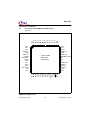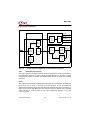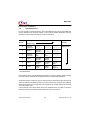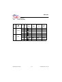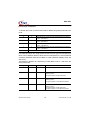
1
0LFURFRPSXWHU&RPSRQHQWV &KLS7HOHWH[WGHFRGHUZLWKHPEHGGHG%LWX& ICs for Consumer Electronics Confidential Preliminary User’s Manual TVTEXT PRO SDA 55xx Version 1.21 July 99 797(;7352 5HYLVLRQ+LVWRU\ 8VHU¶V0DQXDO9HUVLRQ-XO\ Previous Releases: Version 1.1 Dec. 98, Version 1.2 April 99 3DJH 6XEMHFWV See Chapter List of Changes. (GLWLRQ-XO\ 3XEOLVKHGE\,QILQHRQ7HFKQRORJLHV%HUHLFK+DOEOHLWHU0DUNHWLQJ.RPPXQLNDWLRQ %DODQVWUDH'0QFKHQ © Infneon Technologies 1999. All Rights Reserved. As far as patents or other rights of third parties are concerned, liability is only assumed for components per se, not for applications, processes and circuits implemented within components or assemblies. The information describes the type of component and shall not be considered as assured characteristics. Terms of delivery and rights to change design reserved. For questions on technology, delivery and prices please contact the Offices of Infineon Technologies in Germany or Infineon Technologies Companies and Representatives worldwide. Due to technical requirements components may contain dangerous substances. For information on the type in question please contact your nearest Infineon Technolgies Office. SDA 55xx Preliminary & Confidential 1 1.1 1.2 1.3 1.4 1.5 1.6 1.7 Overview . . . . . . . . . . . . . . . . . . . . . . . . . . . . . . . . . . . . . . . . . . . . . . . . . . . .9 Preface . . . . . . . . . . . . . . . . . . . . . . . . . . . . . . . . . . . . . . . . . . . . . . . . . . . . .9 Organization of this document . . . . . . . . . . . . . . . . . . . . . . . . . . . . . . . . . . . .9 Related Documentation . . . . . . . . . . . . . . . . . . . . . . . . . . . . . . . . . . . . . . . .10 Introduction . . . . . . . . . . . . . . . . . . . . . . . . . . . . . . . . . . . . . . . . . . . . . . . . .11 Features . . . . . . . . . . . . . . . . . . . . . . . . . . . . . . . . . . . . . . . . . . . . . . . . . . . .12 Logic Symbol . . . . . . . . . . . . . . . . . . . . . . . . . . . . . . . . . . . . . . . . . . . . . . . .15 Block diagram . . . . . . . . . . . . . . . . . . . . . . . . . . . . . . . . . . . . . . . . . . . . . . .16 2 2.1 2.2 2.3 Package and Pinning . . . . . . . . . . . . . . . . . . . . . . . . . . . . . . . . . . . . . . . . .17 Pin Functions (ROM and ROMless Version) . . . . . . . . . . . . . . . . . . . . . . . .17 Additional Pins or Functions for ROMless Version . . . . . . . . . . . . . . . . . . .20 Port Alternate functions . . . . . . . . . . . . . . . . . . . . . . . . . . . . . . . . . . . . . . . .22 3 3.1 SFR Overview . . . . . . . . . . . . . . . . . . . . . . . . . . . . . . . . . . . . . . . . . . . . . . .27 Additional registers . . . . . . . . . . . . . . . . . . . . . . . . . . . . . . . . . . . . . . . . . . .30 4 4.1 4.2 Clock System . . . . . . . . . . . . . . . . . . . . . . . . . . . . . . . . . . . . . . . . . . . . . . .33 General Function . . . . . . . . . . . . . . . . . . . . . . . . . . . . . . . . . . . . . . . . . . . . .33 Register Description . . . . . . . . . . . . . . . . . . . . . . . . . . . . . . . . . . . . . . . . . .35 5 5.1 5.2 5.2.1 5.2.2 5.3 5.4 5.4.1 5.4.2 5.4.3 5.5 5.5.1 5.5.2 Slicer and Acquisition . . . . . . . . . . . . . . . . . . . . . . . . . . . . . . . . . . . . . . . .39 General Function . . . . . . . . . . . . . . . . . . . . . . . . . . . . . . . . . . . . . . . . . . . . .39 Slicer Architecture . . . . . . . . . . . . . . . . . . . . . . . . . . . . . . . . . . . . . . . . . . . .39 Distortion Processing . . . . . . . . . . . . . . . . . . . . . . . . . . . . . . . . . . . . . . . .40 Data Separation . . . . . . . . . . . . . . . . . . . . . . . . . . . . . . . . . . . . . . . . . . . .41 H/V-Synchronization . . . . . . . . . . . . . . . . . . . . . . . . . . . . . . . . . . . . . . . . . .41 Acquisition Interface . . . . . . . . . . . . . . . . . . . . . . . . . . . . . . . . . . . . . . . . . .42 FC-Check . . . . . . . . . . . . . . . . . . . . . . . . . . . . . . . . . . . . . . . . . . . . . . . . .42 Interrupts . . . . . . . . . . . . . . . . . . . . . . . . . . . . . . . . . . . . . . . . . . . . . . . . .43 VBI Buffer and Memory Organization . . . . . . . . . . . . . . . . . . . . . . . . . . .43 Register Description . . . . . . . . . . . . . . . . . . . . . . . . . . . . . . . . . . . . . . . . . .46 RAM Registers . . . . . . . . . . . . . . . . . . . . . . . . . . . . . . . . . . . . . . . . . . . . .48 Recommended Parameter Settings . . . . . . . . . . . . . . . . . . . . . . . . . . . . .57 6 6.1 6.1.1 6.1.2 6.1.3 6.2 6.3 6.3.1 6.3.2 6.3.3 Microcontroller . . . . . . . . . . . . . . . . . . . . . . . . . . . . . . . . . . . . . . . . . . . . . .59 Architecture . . . . . . . . . . . . . . . . . . . . . . . . . . . . . . . . . . . . . . . . . . . . . . . . .59 CPU-Hardware . . . . . . . . . . . . . . . . . . . . . . . . . . . . . . . . . . . . . . . . . . . .60 CPU Timing . . . . . . . . . . . . . . . . . . . . . . . . . . . . . . . . . . . . . . . . . . . . . . .63 Addressing Modes . . . . . . . . . . . . . . . . . . . . . . . . . . . . . . . . . . . . . . . . . .63 Ports and I/O-Pins . . . . . . . . . . . . . . . . . . . . . . . . . . . . . . . . . . . . . . . . . . . .65 Instruction Set . . . . . . . . . . . . . . . . . . . . . . . . . . . . . . . . . . . . . . . . . . . . . . .68 Notes on Data Addressing Modes . . . . . . . . . . . . . . . . . . . . . . . . . . . . . .68 Notes on Program Addressing Modes . . . . . . . . . . . . . . . . . . . . . . . . . . .68 Instruction Set Description . . . . . . . . . . . . . . . . . . . . . . . . . . . . . . . . .69 Semiconductor Group 3 User’s Manual July 99 SDA 55xx Preliminary & Confidential 6.3.4 Instruction Opcodes in Hexadecimal Order . . . . . . . . . . . . . . . . . . . . . . . 74 7 7.1 7.2 7.3 7.4 7.4.1 7.5 7.6 7.6.1 7.7 7.8 7.9 7.10 7.11 7.12 7.13 7.14 7.15 7.16 Interrupts . . . . . . . . . . . . . . . . . . . . . . . . . . . . . . . . . . . . . . . . . . . . . . . . . . 83 Interrupt System . . . . . . . . . . . . . . . . . . . . . . . . . . . . . . . . . . . . . . . . . . . . . 83 Interrupt Sources . . . . . . . . . . . . . . . . . . . . . . . . . . . . . . . . . . . . . . . . . . . . . 83 Overview . . . . . . . . . . . . . . . . . . . . . . . . . . . . . . . . . . . . . . . . . . . . . . . . . . .84 Enabling interrupts . . . . . . . . . . . . . . . . . . . . . . . . . . . . . . . . . . . . . . . . . . . . 85 Interrupt Enable registers (IE0 IE1 IE2 IE3) . . . . . . . . . . . . . . . . . . . . . . 85 Interrupt source registers . . . . . . . . . . . . . . . . . . . . . . . . . . . . . . . . . . . . . . . 87 Interrupt priority . . . . . . . . . . . . . . . . . . . . . . . . . . . . . . . . . . . . . . . . . . . . . .90 Interrupt Priority registers (IP0 IP1) . . . . . . . . . . . . . . . . . . . . . . . . . . . . .91 Interrupt Vectors . . . . . . . . . . . . . . . . . . . . . . . . . . . . . . . . . . . . . . . . . . . . . 92 Interrupt and memory extension . . . . . . . . . . . . . . . . . . . . . . . . . . . . . . . . . 93 Interrupt Handling . . . . . . . . . . . . . . . . . . . . . . . . . . . . . . . . . . . . . . . . . . . . 93 Interrupt Latency . . . . . . . . . . . . . . . . . . . . . . . . . . . . . . . . . . . . . . . . . . . . . 94 Interrupt Flag Clear . . . . . . . . . . . . . . . . . . . . . . . . . . . . . . . . . . . . . . . . . . . 94 Interrupt return . . . . . . . . . . . . . . . . . . . . . . . . . . . . . . . . . . . . . . . . . . . . . . . 94 Interrupt Nesting . . . . . . . . . . . . . . . . . . . . . . . . . . . . . . . . . . . . . . . . . . . . . 94 External Interrupts . . . . . . . . . . . . . . . . . . . . . . . . . . . . . . . . . . . . . . . . . . . . 95 Extension of Standard 8051 Interrupt Logic . . . . . . . . . . . . . . . . . . . . . . . . 95 Interrupt Task Function . . . . . . . . . . . . . . . . . . . . . . . . . . . . . . . . . . . . . . . .97 8 8.1 8.2 8.3 8.4 8.5 Power Saving modes . . . . . . . . . . . . . . . . . . . . . . . . . . . . . . . . . . . . . . . .99 Power Save mode registers . . . . . . . . . . . . . . . . . . . . . . . . . . . . . . . . . . . . 99 Idle mode . . . . . . . . . . . . . . . . . . . . . . . . . . . . . . . . . . . . . . . . . . . . . . . . . .103 Power down mode . . . . . . . . . . . . . . . . . . . . . . . . . . . . . . . . . . . . . . . . . . .104 Power save mode . . . . . . . . . . . . . . . . . . . . . . . . . . . . . . . . . . . . . . . . . . .104 Slow down mode . . . . . . . . . . . . . . . . . . . . . . . . . . . . . . . . . . . . . . . . . . . .104 9 9.1 9.2 9.3 9.4 9.5 9.6 9.7 9.8 9.9 9.10 9.10.1 9.10.2 Reset . . . . . . . . . . . . . . . . . . . . . . . . . . . . . . . . . . . . . . . . . . . . . . . . . . . . .105 Reset sources . . . . . . . . . . . . . . . . . . . . . . . . . . . . . . . . . . . . . . . . . . . . . .105 Reset filtering . . . . . . . . . . . . . . . . . . . . . . . . . . . . . . . . . . . . . . . . . . . . . . .105 Reset duration . . . . . . . . . . . . . . . . . . . . . . . . . . . . . . . . . . . . . . . . . . . . . .105 Registers . . . . . . . . . . . . . . . . . . . . . . . . . . . . . . . . . . . . . . . . . . . . . . . . . .105 Functional blocks . . . . . . . . . . . . . . . . . . . . . . . . . . . . . . . . . . . . . . . . . . . .105 RAMs . . . . . . . . . . . . . . . . . . . . . . . . . . . . . . . . . . . . . . . . . . . . . . . . . . . . .105 Analog blocks . . . . . . . . . . . . . . . . . . . . . . . . . . . . . . . . . . . . . . . . . . . . . .106 Processor . . . . . . . . . . . . . . . . . . . . . . . . . . . . . . . . . . . . . . . . . . . . . . . . .106 Ports . . . . . . . . . . . . . . . . . . . . . . . . . . . . . . . . . . . . . . . . . . . . . . . . . . . . .106 Initialization phase . . . . . . . . . . . . . . . . . . . . . . . . . . . . . . . . . . . . . . . . . . .106 Acquisition . . . . . . . . . . . . . . . . . . . . . . . . . . . . . . . . . . . . . . . . . . . . . . .106 Display . . . . . . . . . . . . . . . . . . . . . . . . . . . . . . . . . . . . . . . . . . . . . . . . . .106 10 10.1 Memory Organization . . . . . . . . . . . . . . . . . . . . . . . . . . . . . . . . . . . . . . .107 Program Memory . . . . . . . . . . . . . . . . . . . . . . . . . . . . . . . . . . . . . . . . . . . .107 Semiconductor Group 4 User’s Manual July 99 SDA 55xx Preliminary & Confidential 10.2 10.2.1 10.2.2 10.3 10.3.1 10.3.2 10.3.3 10.3.4 10.3.5 10.3.6 10.3.7 10.3.8 10.3.9 10.3.10 Internal Data RAM . . . . . . . . . . . . . . . . . . . . . . . . . . . . . . . . . . . . . . . . . . .108 CPU RAM . . . . . . . . . . . . . . . . . . . . . . . . . . . . . . . . . . . . . . . . . . . . . . .108 Extended Data RAM(XRAM) . . . . . . . . . . . . . . . . . . . . . . . . . . . . . . . . .109 Memory Extension . . . . . . . . . . . . . . . . . . . . . . . . . . . . . . . . . . . . . . . . . . .109 Memory extension registers . . . . . . . . . . . . . . . . . . . . . . . . . . . . . . . . . .110 Reset value . . . . . . . . . . . . . . . . . . . . . . . . . . . . . . . . . . . . . . . . . . . . . .112 Program memory Banking (LJMP) . . . . . . . . . . . . . . . . . . . . . . . . . . . .112 CALLs and Interrupts . . . . . . . . . . . . . . . . . . . . . . . . . . . . . . . . . . . . . . .113 Stack Full . . . . . . . . . . . . . . . . . . . . . . . . . . . . . . . . . . . . . . . . . . . . . . . .113 Timing . . . . . . . . . . . . . . . . . . . . . . . . . . . . . . . . . . . . . . . . . . . . . . . . . .113 Interfacing Extended memory . . . . . . . . . . . . . . . . . . . . . . . . . . . . . . . .114 Interfacing Extended stack . . . . . . . . . . . . . . . . . . . . . . . . . . . . . . . . . .114 Application Examples . . . . . . . . . . . . . . . . . . . . . . . . . . . . . . . . . . . . . .114 ROM and ROMless version. . . . . . . . . . . . . . . . . . . . . . . . . . . . . . . . . .116 11 11.1 11.2 UART . . . . . . . . . . . . . . . . . . . . . . . . . . . . . . . . . . . . . . . . . . . . . . . . . . . . .117 Modes . . . . . . . . . . . . . . . . . . . . . . . . . . . . . . . . . . . . . . . . . . . . . . . . . . . .117 Multiprocessor Communication . . . . . . . . . . . . . . . . . . . . . . . . . . . . . . . . .119 12 12.1 12.1.1 12.1.2 12.1.3 General Purpose Timers/Counters . . . . . . . . . . . . . . . . . . . . . . . . . . . .121 Timer/Counter 0: Mode Selection . . . . . . . . . . . . . . . . . . . . . . . . . . . . . . .121 Configuring the Timer/Counter Input . . . . . . . . . . . . . . . . . . . . . . . . . . .122 Timer/Counter Mode Register . . . . . . . . . . . . . . . . . . . . . . . . . . . . . . . .123 Timer/Counter Control Register . . . . . . . . . . . . . . . . . . . . . . . . . . . . . . .124 13 13.1 13.2 13.3 13.3.1 13.3.2 13.3.3 13.3.4 13.3.5 13.3.6 13.3.7 13.3.8 13.3.9 13.3.10 13.3.11 13.3.12 13.4 13.5 13.6 Capture reload timer . . . . . . . . . . . . . . . . . . . . . . . . . . . . . . . . . . . . . . . .125 Input clock . . . . . . . . . . . . . . . . . . . . . . . . . . . . . . . . . . . . . . . . . . . . . . . . .125 Reset values . . . . . . . . . . . . . . . . . . . . . . . . . . . . . . . . . . . . . . . . . . . . . . .125 Functional description . . . . . . . . . . . . . . . . . . . . . . . . . . . . . . . . . . . . . . . .125 Port pin . . . . . . . . . . . . . . . . . . . . . . . . . . . . . . . . . . . . . . . . . . . . . . . . .125 Slow down mode . . . . . . . . . . . . . . . . . . . . . . . . . . . . . . . . . . . . . . . . . .125 Run . . . . . . . . . . . . . . . . . . . . . . . . . . . . . . . . . . . . . . . . . . . . . . . . . . . .126 Overflow . . . . . . . . . . . . . . . . . . . . . . . . . . . . . . . . . . . . . . . . . . . . . . . . .126 Modes . . . . . . . . . . . . . . . . . . . . . . . . . . . . . . . . . . . . . . . . . . . . . . . . . .126 Normal Capture mode . . . . . . . . . . . . . . . . . . . . . . . . . . . . . . . . . . . . . .126 Polling mode . . . . . . . . . . . . . . . . . . . . . . . . . . . . . . . . . . . . . . . . . . . . .127 Capture mode with spike suppression at the start of a telegram . . . . . .127 First event . . . . . . . . . . . . . . . . . . . . . . . . . . . . . . . . . . . . . . . . . . . . . . .127 Second event . . . . . . . . . . . . . . . . . . . . . . . . . . . . . . . . . . . . . . . . . . . . .127 CRT Interrupt. . . . . . . . . . . . . . . . . . . . . . . . . . . . . . . . . . . . . . . . . . . . .128 Counter Stop . . . . . . . . . . . . . . . . . . . . . . . . . . . . . . . . . . . . . . . . . . . . .128 Idle and power down mode. . . . . . . . . . . . . . . . . . . . . . . . . . . . . . . . . . . . .128 Registers . . . . . . . . . . . . . . . . . . . . . . . . . . . . . . . . . . . . . . . . . . . . . . . . . .128 Time resolution . . . . . . . . . . . . . . . . . . . . . . . . . . . . . . . . . . . . . . . . . . . . .131 Semiconductor Group 5 User’s Manual July 99 SDA 55xx Preliminary & Confidential 13.7 Block diagram . . . . . . . . . . . . . . . . . . . . . . . . . . . . . . . . . . . . . . . . . . . . . .132 14 14.1 14.2 14.3 14.4 14.4.1 14.4.2 14.5 14.6 14.7 14.8 Pulse Width Modulation Unit . . . . . . . . . . . . . . . . . . . . . . . . . . . . . . . . .133 Reset Values . . . . . . . . . . . . . . . . . . . . . . . . . . . . . . . . . . . . . . . . . . . . . . .133 Input clock . . . . . . . . . . . . . . . . . . . . . . . . . . . . . . . . . . . . . . . . . . . . . . . . .133 Port pins . . . . . . . . . . . . . . . . . . . . . . . . . . . . . . . . . . . . . . . . . . . . . . . . . .133 Functional description . . . . . . . . . . . . . . . . . . . . . . . . . . . . . . . . . . . . . . . .134 8 bit PWM . . . . . . . . . . . . . . . . . . . . . . . . . . . . . . . . . . . . . . . . . . . . . . .134 14 bit PWM . . . . . . . . . . . . . . . . . . . . . . . . . . . . . . . . . . . . . . . . . . . . . .135 Cycle time . . . . . . . . . . . . . . . . . . . . . . . . . . . . . . . . . . . . . . . . . . . . . . . . .136 Power down, idle and Power save mode. . . . . . . . . . . . . . . . . . . . . . . . . .136 Timer . . . . . . . . . . . . . . . . . . . . . . . . . . . . . . . . . . . . . . . . . . . . . . . . . . . . .136 Control registers . . . . . . . . . . . . . . . . . . . . . . . . . . . . . . . . . . . . . . . . . . . .137 15 15.1 15.2 15.3 15.4 15.5 15.6 15.7 15.8 Watchdog Timer . . . . . . . . . . . . . . . . . . . . . . . . . . . . . . . . . . . . . . . . . . .141 Input clock . . . . . . . . . . . . . . . . . . . . . . . . . . . . . . . . . . . . . . . . . . . . . . . . .141 Starting WDT . . . . . . . . . . . . . . . . . . . . . . . . . . . . . . . . . . . . . . . . . . . . . . .141 Refresh . . . . . . . . . . . . . . . . . . . . . . . . . . . . . . . . . . . . . . . . . . . . . . . . . . .141 WDT reset . . . . . . . . . . . . . . . . . . . . . . . . . . . . . . . . . . . . . . . . . . . . . . . . .142 Power down mode . . . . . . . . . . . . . . . . . . . . . . . . . . . . . . . . . . . . . . . . . . .142 Time period . . . . . . . . . . . . . . . . . . . . . . . . . . . . . . . . . . . . . . . . . . . . . . . .143 Block Diagram . . . . . . . . . . . . . . . . . . . . . . . . . . . . . . . . . . . . . . . . . . . . . .144 WDT as general purpose timer. . . . . . . . . . . . . . . . . . . . . . . . . . . . . . . . . .145 16 16.1 16.2 Analog Digital Converter (CADC) . . . . . . . . . . . . . . . . . . . . . . . . . . . . . .147 Power Down and Wake Up . . . . . . . . . . . . . . . . . . . . . . . . . . . . . . . . . . . .147 Register Description . . . . . . . . . . . . . . . . . . . . . . . . . . . . . . . . . . . . . . . . .147 17 17.1 17.1.1 17.1.2 17.2 Sync System . . . . . . . . . . . . . . . . . . . . . . . . . . . . . . . . . . . . . . . . . . . . . .153 General Description . . . . . . . . . . . . . . . . . . . . . . . . . . . . . . . . . . . . . . . . . .153 Screen Resolution. . . . . . . . . . . . . . . . . . . . . . . . . . . . . . . . . . . . . . . . .153 Sync Interrupts . . . . . . . . . . . . . . . . . . . . . . . . . . . . . . . . . . . . . . . . . . .155 Register Description . . . . . . . . . . . . . . . . . . . . . . . . . . . . . . . . . . . . . . . . .156 18 18.1 18.2 18.3 18.3.1 18.3.2 18.3.3 18.3.4 18.4 18.4.1 18.4.2 Display . . . . . . . . . . . . . . . . . . . . . . . . . . . . . . . . . . . . . . . . . . . . . . . . . . .170 Display Features . . . . . . . . . . . . . . . . . . . . . . . . . . . . . . . . . . . . . . . . . . . .170 Display Memory . . . . . . . . . . . . . . . . . . . . . . . . . . . . . . . . . . . . . . . . . . . . .171 Parallel Character Attributes . . . . . . . . . . . . . . . . . . . . . . . . . . . . . . . . . . .172 Access of Characters . . . . . . . . . . . . . . . . . . . . . . . . . . . . . . . . . . . . . .173 Flash . . . . . . . . . . . . . . . . . . . . . . . . . . . . . . . . . . . . . . . . . . . . . . . . . . .176 Character Individual Double Height . . . . . . . . . . . . . . . . . . . . . . . . . . . .176 Character Individual Double Width . . . . . . . . . . . . . . . . . . . . . . . . . . . .178 Global OSD Attributes . . . . . . . . . . . . . . . . . . . . . . . . . . . . . . . . . . . . . . . .179 Character Display Area Resolution . . . . . . . . . . . . . . . . . . . . . . . . . . . .183 Cursor . . . . . . . . . . . . . . . . . . . . . . . . . . . . . . . . . . . . . . . . . . . . . . . . . .184 Semiconductor Group 6 User’s Manual July 99 SDA 55xx Preliminary & Confidential 18.4.3 18.4.4 18.4.5 18.4.6 18.4.7 18.4.8 18.4.9 18.4.10 18.5 18.5.1 18.6 18.6.1 18.6.2 18.6.3 18.6.4 18.6.5 Border Color . . . . . . . . . . . . . . . . . . . . . . . . . . . . . . . . . . . . . . . . . . . . .187 Full Screen Double Height . . . . . . . . . . . . . . . . . . . . . . . . . . . . . . . . . . .188 Flash Rate Control . . . . . . . . . . . . . . . . . . . . . . . . . . . . . . . . . . . . . . . . .190 Transparency of Boxes . . . . . . . . . . . . . . . . . . . . . . . . . . . . . . . . . . . . .191 CLUT . . . . . . . . . . . . . . . . . . . . . . . . . . . . . . . . . . . . . . . . . . . . . . . . . . .194 Character Resolution . . . . . . . . . . . . . . . . . . . . . . . . . . . . . . . . . . . . . . .199 Shadowing . . . . . . . . . . . . . . . . . . . . . . . . . . . . . . . . . . . . . . . . . . . . . . .201 Progressive Scan . . . . . . . . . . . . . . . . . . . . . . . . . . . . . . . . . . . . . . . . . .202 DRCS characters . . . . . . . . . . . . . . . . . . . . . . . . . . . . . . . . . . . . . . . . . . . .203 Memory Organization of DRCS characters . . . . . . . . . . . . . . . . . . . . . .203 Memory Organization . . . . . . . . . . . . . . . . . . . . . . . . . . . . . . . . . . . . . . . .206 Character Display Area . . . . . . . . . . . . . . . . . . . . . . . . . . . . . . . . . . . . .208 CLUT Area . . . . . . . . . . . . . . . . . . . . . . . . . . . . . . . . . . . . . . . . . . . . . . .208 Global Display Word/Cursor . . . . . . . . . . . . . . . . . . . . . . . . . . . . . . . . .208 1-bit/2-bit/4-bit DRCS character . . . . . . . . . . . . . . . . . . . . . . . . . . . . . . .209 Overview on the SFR registers . . . . . . . . . . . . . . . . . . . . . . . . . . . . . . .210 19 19.1 D/A Converter . . . . . . . . . . . . . . . . . . . . . . . . . . . . . . . . . . . . . . . . . . . . . .211 Register Description . . . . . . . . . . . . . . . . . . . . . . . . . . . . . . . . . . . . . . . . .211 20 20.1 20.2 20.3 20.4 20.5 Electrical Characteristics . . . . . . . . . . . . . . . . . . . . . . . . . . . . . . . . . . . .215 Absolute Maximum Ratings . . . . . . . . . . . . . . . . . . . . . . . . . . . . . . . . . . . .215 Operating Range . . . . . . . . . . . . . . . . . . . . . . . . . . . . . . . . . . . . . . . . . . . .215 DC Characteristics . . . . . . . . . . . . . . . . . . . . . . . . . . . . . . . . . . . . . . . . . . .215 Timings . . . . . . . . . . . . . . . . . . . . . . . . . . . . . . . . . . . . . . . . . . . . . . . . . . .221 Package Outlines . . . . . . . . . . . . . . . . . . . . . . . . . . . . . . . . . . . . . . . . . . . .224 21 Glossary . . . . . . . . . . . . . . . . . . . . . . . . . . . . . . . . . . . . . . . . . . . . . . . . . .225 22 Index . . . . . . . . . . . . . . . . . . . . . . . . . . . . . . . . . . . . . . . . . . . . . . . . . . . . .226 23 List of changes since last edition . . . . . . . . . . . . . . . . . . . . . . . . . . . . .227 Semiconductor Group 7 User’s Manual July 99 SDA 55xx Preliminary & Confidential Semiconductor Group 8 User’s Manual July 99 SDA 55xx Overview Preliminary & Confidential 1 Overview 1.1 Preface TVText Pro is a 8-bit controller based on SIEMENS Enhanced 8051 core with embedded teletext, On screen Display and TV controller functions. TVText Pro can be used for a wide range of TV and OSD applications. This document provides complete reference information of the TVText Pro system. 1.2 Organization of this document • Chapter 1, Overview Gives a general description of the product and lists the key features. • Chapter 2, Package and Pinning Lists pin locations with associated signals, categorizes signals according to function, and describes signals. • Chapter 3, SFR Overview List of the registers. • Chapter 4, Clock System Describes Clock system and it’s distribution • Chapter 5, Slicer and Acquisition Describes slicer and acquisiton interface • Chapter 6, Microcontroller Describes microcontroller, instruction set, ports • Chapter 7, Interrupts Describes interrupts, priorities, sources, enhancements to standard 8051 interrupt logic. • Chapter 8, Power Saving modes Describes the four power saving modes of the device. • Chapter 9, Reset Describes reset requirements and behavior of the device • Chapter 10, Memory Organization Describes internal/external RAM, ROM and Memory extension • Chapter 11, UART Describes peripheral UART • Chapter 12, General Purpose Timers/Counters Describes peripherals Timer0 and timer 1 Semiconductor Group 9 User’s Manual July 99 SDA 55xx Overview Preliminary & Confidential • Chapter 13, Capture reload timer Describes peripheral CRT • Chapter 14, Pulse Width Modulation Unit Describes peripheral PWM • Chapter 15, Watchdog Timer Describes peripheral Watchdog timer • Chapter 16, Analog to Digital converter Describes ADC functionality. • Chapter 17, Sync System Screen resolution, sync mechanism • Chapter 18, Display Display features, modes and their usage • Chapter 19, Digital to Anaog converter Describes DAC operation • Chapter 20, Electrical Characteristics Lists all important AC and DC Values and the maximum operating conditions of SDA55xx. • Chapter 21,22 &23 Glossary, Index and List of changes since last edition Provides a list of used terms and abbreviations, their explanation and where to find them in that document and changes since last edition 1.3 Related Documentation For easier understanding of this specification it is recommended to read the documentation listed in the following table. Document Name Semiconductor Group Document Purpose 10 User’s Manual July 99 SDA 55xx Overview Preliminary & Confidential 1.4 Introduction The SDA 55xx is a single chip teletext decoder for decoding World System Teletext data as well as Video Programming System (VPS), Program Delivery Control (PDC), and Wide Screen Signalling (WSS) data used for PAL plus transmissions (line 23). The device provides an integrated general-purpose, fully 8051-compatible Microcontroller with television specific hardware features. Microcontroller has been enhanced to provide powerful features such as memory banking, data pointers and additional interrupts etc. The on-chip display unit for displaying Level 1.5 teletext data can also be used for customer defined on-screen displays. Internal XRAM consists of up to 16 KBytes. Device has an internal ROM of up to 128 KBytes. ROMless versions can access up to 1MByte of external RAM and ROM. The SDA 55xx supports a wide range of standards including PAL, NTSC and contains a digital slicer for VPS, WSS, PDC, and TTX, an accelerating acquisition hardware module, a display generator for Level 1.5 TTX data and powerful On screen Display capabilities based on parallel attributes, and Pixel oriented characters (DRCS) The 8 bit Microcontroller runs at 360 ns. cycle time (min.). Controller with dedicated hardware does most of the internal TTX acquisition processing, transfers data to/from the external memory interface and receives/transmits data via I2C-firmware userinterface. The slicer combined with dedicated hardware stores TTX data in a VBI buffer of 1 Kilobyte. The Microcontroller firmware performs all the acquisition tasks (hamming- and parity-checks, page search and evaluation of header control bits) once per field. Additionally, the firmware can provide high-end Teletext-features like Packet-26handling, FLOF, TOP and list-pages. The interface to the user software is optimized for minimal overhead. SDA 55xx is realized in 0.25 micron technology with 2.5V supply voltage and 3.3V I/O (TTL compatible). The software and hardware development environment (TEAM) is available to simplify and speed up the development of the software and On Screen Display. TEAM stands for: TVT Expert Application Maker. It improves the TV controller software quality in following aspects: • • • • • • • Shorter time to market Re-usability Target independent development Verification and validation before targeting General test concept Graphical interface design requiring minimum programming and controller know how Modular and open tool chain, configurable by customer Semiconductor Group 11 User’s Manual July 99 SDA 55xx Overview Preliminary & Confidential CMOS 1.5 Features General • Feature selection via special function register • Simultaneous reception of TTX, VPS, PDC, and WSS (line 23) • Supply Voltage 2.5 and 3.3 V • ROM version package P-SDIP 52, P-MQFP64 • Romless version package P-MQFP100,P-LCC84 P-SDIP-52 External Crystal and Programmable clock speed • Single external 6MHz crystal, all necessary clocks are generated internally • CPU clock speed selectable via special function registers. • Normal Mode 33.33 Mhz CPU clock, Power Save mode 8.33 Mhz P-MQFP-64 Microcontroller Features • • • • • • • • • 8bit 8051 instruction set compatible CPU. 33.33-MHz internal clock (max.) 0.360 µs (min.) instruction cycle Two 16-bit timers Watchdog timer Capture compare timer for infrared remote control decoding Pulse width modulation unit (2 channels 14 bit, 6 channels 8 bit) ADC (4 channels, 8 bit) UART Type Package TVTEXT PRO (ROM) P-SDIP-52, P-MQFP-64 TVTEXT PRO (ROMless) P-MQFP-100, P-LCC-84 Semiconductor Group 12 User’s Manual July 99 SDA 55xx Overview Preliminary & Confidential Memory • • • • • • • Non-multiplexed 8-bit data and 16 … 20-bit address bus (ROMless Version) Memory banking up to 1Mbyte (Romless version) Up to 128 Kilobyte on Chip Program ROM Eight 16-bit data pointer registers (DPTR) 256-bytes on-chip Processor Internal RAM (IRAM) 128bytes extended stack memory. Display RAM and TXT/VPS/PDC/WSS-Acquisition-Buffer directly accessible via MOVX • UP to 16KByte on Chip Extended RAM(XRAM) consisting of; - 1 Kilobyte on-chip ACQ-buffer-RAM (access via MOVX) - 1 Kilobyte on-chip extended-RAM (XRAM, access via MOVX) for user software - 3 Kilobyte Display Memory Display Features • • • • • • • • • • • • • • • • • • • ROM Character Set Supports all East and West European Languages in single device Mosaic Graphic Character Set Parallel Display Attributes Single/Double Width/Height of Characters Variable Flash Rate Programmable Screen Size (25 Rows x 33...64 Columns) Flexible Character Matrixes (HxV) 12 x 9...16 Up to 256 Dynamical Redefinable Characters in standard mode; 1024 Dynamical Redefinable Characters in Enhanced Mode CLUT with up to 4096 color combinations Up to 16 Colors per DRCS Character One out of Eight Colors for Foreground and Background Colors for 1-bit DRCS and ROM Characters Shadowing Contrast Reduction Pixel by Pixel Shiftable Cursor With up to 4 Different Colors Support of Progressive Scan and 100 Hz. 3 X 4Bits RGB-DACs On-Chip Free Programmable Pixel Clock from 10 MHZ to 32MHz Pixel Clock Independent from CPU Clock Multinorm H/V-Display Synchronization in Master or Slave Mode Semiconductor Group 13 User’s Manual July 99 SDA 55xx Overview Preliminary & Confidential Acquisition Features • • • • • • • • • • • Multistandard Digital Data Slicer Parallel Multi-norm Slicing (TTX, VPS, WSS, CC, G+) Four Different Framing Codes Available Data Caption only Limited by available Memory Programmable VBI-buffer Full Channel Data Slicing Supported Fully Digital Signal Processing Noise Measurement and Controlled Noise Compensation Attenuation Measurement and Compensation Group Delay Measurement and Compensation Exact Decoding of Echo Disturbed Signals Ports • • • • • One 8-bit I/O-port with open drain output and optional I2C Bus emulation suport(Port0) Two 8-bit multifunction I/O-ports (Port1, Port3) One 4-bit port working as digital or analog inputs for the ADC (Port2) One 2-bit I/O port with secondary functions (P4.2, 4.3, 4.7) One 4-bit I/O-port with secondary function (P4.0, 4.1, 4.4) (Not available in P-SDIP 52) Semiconductor Group 14 User’s Manual July 99 SDA 55xx Overview Preliminary & Confidential 1.6 Logic Symbol vcc(2.5,3.3) vss XTAL1 Address 20 bit XTAL2 STOP Data 8 bit ENE OCF CVBS Port 0 8 bit ALE PSEN R G Port 1 8 bit TVTEXT PRO B Port 2 4 bit COR_BLA HSYNC/SSC Port 3 8 bit VSYNC RD WR RST Semiconductor Group Port 4 6 bit 15 User’s Manual July 99 Semiconductor Group 16 6)5V 8$57 3RUW/RJLF 3:0 &DSWXUHFRQWURO :'7 6\VWHP 6\QF &ORFN ,QWHUIDFH %XV 3HULSKHUDO LQWHUIDFH $'& ; ,5$0 Counter 1 Counter 0 ; 0HPRU\ ([WHQVLRQ 6WDFN A[16 to A20] Interrupt Controller Core 06 Memory Extension Unit ADCX4 .; 3URJUDP520 $'& $'& CVBS Display Regs DAC’s FIFO CLUT 'LVSOD\*HQHUDWRU Display logic RAM/ROM Interface $UELWHU %XV $FTXLVLWLRQLQWHUIDFH $FTXLVLWLRQ 6OLFHU R 65$0 ;5$0 Imran Hajimusa HL IV CE COR_BLA H V .; &KDUDFWHU 520 .[ELW 1.7 B Preliminary & Confidential G $QDORJ0X[ SDA 55xx Overview Block diagram User’s Manual July 99 A[0 to 15] D[0 to 7] ALE PSEN RD WR P[0 to 4] SDA 55xx Package and Pinning Preliminary & Confidential 2 Package and Pinning 2.1 Pin Functions (ROM and ROMless Version) 6\PERO )XQFWLRQ 33 Type Additional reference I/O Available: SDIP52,MQFP64, MQFP100,PLCC84 Port 0 is a 8-bit open drain bidirectional I/O-port. Port 0 pins that have 1 written to them float; in this state they can be used as high impedance inputs (e.g. for software driven I 2C Bus support). 33 3:0 33 $'& 33 Type Additional reference I/O Available: SDIP52,MQFP64, MQFP100,PLCC84 Port 1 is a 8-bit bidirectional multifunction I/O port with internal pull-up resistors. Port 1 pins that have 1 written to them are pulled high by the internal pull-up resistors and in that state can be used as inputs. The secondary functions of port 1 pins are: Port bits P1.0 - P1.5 contain the 6 output channels of the 8-bit pulse width modulation unit. Port bits P1.6 - P1.7 contain the two output channels of the 14bit pulse width modulation unit. Type Additional reference I Available: SDIP52,MQFP64, MQFP100,PLCC84 Port 2 is a 4-bit input port without pull-up resistors. Port 2 also works as analog input for the 4-channel-ADC. Type Additional reference I/O Available: SDIP52,MQFP64, MQFP100,PLCC84 Port 3 is an 8-bit bidirectional I/O port with internal pull-up resistors. Port 3 pins that have 1 written to them are pulled high by the internal pull-up resistors and in that state can be used as inputs. To use the secondary functions of Port 3, the corresponding output latch must be programmed to a one (1) for that function to operate. The secondary functions are as follows: $OWHUQDWHIXQFWLRQ Semiconductor Group P3.0: ODD/EVEN indicate output P3.1: external extra interrupt 0 (INTX0)/UART(TXD) P3.2: interrupt 0 input/timer 0 gate control input (INT0) P3.3: interrupt 1 input/timer 1 gate control input (INT1) P3.4: counter 0 input (T0) P3.5: counter 1 input (T1) or In master mode HS or VCS output. P3.7 external extra interrupt 0 (INTX1)/UART(RXD) 17 User’s Manual July 99 SDA 55xx Package and Pinning Preliminary & Confidential 6\PERO )XQFWLRQ 333 Type Additional reference I/O Available: SDIP52,MQFP64, MQFP100,PLCC84 Port 4 is a bidirectional I/O port with internal pull-up resistors. Port 4 pins that have 1 written to them are pulled high by the internal pull-up resistors and in that state can be used as inputs. Secondary functions P4.2: RD, Read line. This signal is same as the to output of the pin RD available in some packages. P4.3: WR, write line. This signal is same as the output of the pin WR, which is only available in some package. P4.7: VS, Vertical sync: ODD/Even, Odd/even field indicator. 567 Type Additional reference Available: SDIP52,MQFP64, MQFP100,PLCC84 I A low level on this pin resets the device. An internal pull-up resistor permits power-on reset using only one external capacitor connected to VSS. 9 9 '' 9 '' 66 Type Additional reference PS Available: SDIP52,MQFP64, MQFP100,PLCC84 Input/output (3.3V) Supply voltage (2.5V) Ground (0 V) V V V '' '' VV V V ''$ 66$ Type Additional reference PS Available: SDIP52,MQFP64, MQFP100,PLCC84 Supply voltage for analog components. Ground for analog components. &9%6 Type Additional reference I Available: SDIP52,MQFP64, MQFP100,PLCC84 CVBS input for the acquisition circuit. +66& Type Additional reference I Available: SDIP52,MQFP64, MQFP100,PLCC84 In slave mode Horizontal sync input or sandcastle input for display synchronization.In master mode HS or VCS output. ;7$/ Type Additional reference I Available: SDIP52,MQFP64, MQFP100,PLCC84 Input of the inverting oscillator amplifier. Semiconductor Group 18 User’s Manual July 99 SDA 55xx Package and Pinning Preliminary & Confidential 6\PERO )XQFWLRQ ;7$/ Type Additional reference O Available: SDIP52,MQFP64, MQFP100,PLCC84 Output of the inverting oscillator amplifier. 963 Type Additional reference I/O Available: SDIP52,MQFP64, MQFP100,PLCC84 Vertical sync input/output for display synchronization. Can also be used as digital input P4.7. Furthermore this pin can be selected as an ODD/EVEN indicator alternatively to P3.0. 5*% Type Additional reference O Available: SDIP52,MQFP64, MQFP100,PLCC84 Red, Green, Blue &25B%/$ Type Additional reference O Available: SDIP52,MQFP64, MQFP100,PLCC84 Contrast reduction and blanking Semiconductor Group 19 User’s Manual July 99 SDA 55xx Package and Pinning Preliminary & Confidential 2.2 Additional Pins or Functions for ROMless Version 6\PERO )XQFWLRQ $$ Type Additional reference Available: O MQFP100, PLCC84 Address bus for external program memory or data RAM $$ 333 Type Additional reference Available: I/O MQFP100, PLCC84 After power-on P4.0, P4.1, P4.4 work as additional address lines A17...A19. In port mode, these port lines act as bidirectional I/O port with internal pull-up resistors. Port pins that have ’1’ written to them are pulled high by the internal pull-up resistors and in that state can be used as inputs. '' Type Additional reference Available: I/O MQFP100, PLCC84 Data bus for external memory or data RAM 6723 Type Additional reference I Available: MQFP100 STOP Emulation control line; Driving a low level during the input phase freezes the real time relevant internal peripherals such as timers and interrupt controller. 2&) Type Additional reference O Available: MQFP100 Opcode Fetch Emulation control line; A high level driven by the controller during output phase indicates the beginning of a new instruction. (1( Type Additional reference I Available: MQFP100 Enable Emulation Only if this pin is set to zero externally, STOP and OCF are operational. ENE has an internal pull-up resistor which switches automatically to non-emulation mode if ENE is not connected. Semiconductor Group 20 User’s Manual July 99 SDA 55xx Package and Pinning Preliminary & Confidential 6\PERO )XQFWLRQ 5' Type Additional reference O Available: MQFP100, PLCC84 Control output; indicates a read access to the internal XRAM; can be used for latching data from the data bus into an external data RAM by a MOVX instruction. This signal is also available as P4.2. :5 Type Additional reference O Available: MQFP100, PLCC84 Control output; indicates a write access to the internal XRAM; can be used as a write strobe for writing data into an external data RAM by a MOVX instruction. This signal is also available as P4.3 $/( Type Additional reference O Available: MQFP100 Address Latch Enable 36(1 Type Additional reference O Available: MQFP100, PLCC84 Program Store Enable is a control output signal which is usually connected to OE input line of the external program memory to enable the data output. ;520 Type I Additional Reference Available: MQFP100, PLCC84 This pin must be pulled low to access external ROM. )/B[[ Type I Additional Reference Available: MQFP100 All the pins prefix by FL_ are test pins which must be left open.. Semiconductor Group 21 User’s Manual July 99 SDA 55xx Package and Pinning Preliminary & Confidential 2.3 Port Port Alternate functions I/O Default function Alternate Function 2 Alternate Function 3 Toggle Function Toggle Function Control bit Function Control bit Function P0(0..7) I/O Port pin P1(0) I/O Port pin PWME(E0) PWM 8 bit channel 0 P1(1) I/O Port pin PWME(E1) PWM 8 bit channel 1 P1(2) I/O Port pin PWME(E2) PWM 8 bit channel 2 P1(3) I/O Port pin PWME(E3) PWM 8 bit channel 3 P1(4) I/O Port pin PWME(E4) PWM 8 bit channel 4 P1(5) I/O Port pin PWME(E5) PWM 8 bit channel 5 P1(6) I/O Port pin PWME(E6) PWM 14 bit channel 0 P1(7) I/O Port pin PWME(E7) PWM 14 bit channel 1 P2(0) I Port pin CADCCO(AD0) ADC channel 0 P2(1) I Port pin CADCCO(AD1) ADC channel 1 P2(2) I Port pin CADCCO(AD2) ADC channel 2 P2(3) I Port pin CADCCO(AD3) ADC channel 3 P3(0) I/O Port pin CSCR0(O_E_P3_0) ODD/Even indicator P3(1) I/O Port pin Port input mode External extra Int 0 P3(2) I/O Port pin Port input mode External interrupt 0 P3(3) I/O Port pin Port input mode External interrupt 1 P3(4) I/O Port pin Port input mode Timer/counter 0 input P3(5) I/O Port pin Port input mode Timer/counter 0 input P3(6) I/O Port pin P3(7) I/O Port pin Port input mode External extra Int 1 P4(0)1) I/O A17 CSCR1(A17_P4_0) Port pin P4(1)1) I/O A18 CSCR1(A18_P4_1) Port pin P4(2) I/O Port pin CSCR1(ENARW) Read signal P4(3) I/O Port pin CSCR1(ENARW) Write signal P4(4)1) I/O A19 CSCR1(A19_P4_4) Port pin P4(7) I/O Port/VS in CSCR0(VS_OE, P4_7_ALT) VS output Port output mode TXD Port input mode RXD CSCR0( VS_OE, OddEven output P4_7_ALT) 1) Not available in SDIP52 Semiconductor Group 22 User’s Manual July 99 SDA 55xx Package and Pinning Preliminary & Confidential 3LQ&RQILJXUDWLRQ36',35209HUVLRQ (top view) P0.0 P0.1 P0.2 P0.3 P0.4 P0.5 P0.6 P0.7 VDD 2.5 VSS VDD 3.3 CVBS VDDA 2.5 VSSA P2.0 P2.1 P2.2 P2.3 HS / SSC VS P3.0 P3.1 P3.2 P3.3 P3.4 P3.5 1 36',3 52 2 51 3 50 4 49 5 48 6 47 7 46 8 45 9 44 10 43 11 12 13 14 42 797(;7352 6'$;; 36',3 41 40 39 15 38 16 37 17 36 18 35 19 34 20 33 21 32 22 31 23 30 24 29 25 28 26 27 P1.7 P1.6 P1.5 P1.4 P1.3 P1.2 P1.1 P1.0 VDD 3.3 VSS VDD 2.5 BLANK / COR B G R VDDA 2.5 VSSA XTAL1 XTAL2 RST P4.3 P4.2 VDD 3.3 VSS P3.7 P3.6 )LJXUH 36',35209HUVLRQRI6'$[[ Semiconductor Group 23 User’s Manual July 99 SDA 55xx Package and Pinning Preliminary & Confidential 3LQ&RQILJXUDWLRQ304)35209HUVLRQ (top view) N.C. P0.6 P0.5 P0.4 P0.3 P0.2 P0.1 P0.0 P1.7 P1.6 P1.5 P1.4 P1.3 P1.2 N.C. N.C. 304)3 N.C. N.C. P0.7 VDD 2.5 VSS VDD 3.3 CVBS VDDA 2.5 VSSA P2.0 P2.1 P2.2 P2.3 HS / SSC VS N.C. N.C. N.C. P3.0 P3.1 P3.2 P3.3 P3.4 P3.5 P3.6 P3.7 VSS VDD 3.3 P4.2 P4.3 RST N.C. TVTEXT PRO SDA 55XX P-MQFP-64 N.C. P1.1 P1.0 VDD 3.3 VSS VDD 2.5 BLANK / COR B G R VDDA 2.5 VSSA XTAL1 XTAL2 N.C. N.C. )LJXUH 304)35209HUVLRQ Semiconductor Group 24 User’s Manual July 99 SDA 55xx Package and Pinning Preliminary & Confidential 3LQ&RQILJXUDWLRQ304)3520OHVV9HUVLRQ (top view) D5 D0 D6 A0 D7 FL_CE A1 A2 VDD 3.3 VSS A10 A3 PSEN ALE A4 A11 A5 A9 A6 A8 D1 D4 D2 D3 XROM VDD 2.5 VSS VDD 3.3 P0.0 P0.1 P0.2 P0.3 P0.4 P0.5 P0.6 P0.7 ENE STOP OCF EXTIF CVBS VDDA 2.5 VSSA P2.0 P2.1 P2.2 P2.3 FL_RST A7 A13 A12 A14 VDD 3.3 VSS VDD 2.5 FL_PGM A15 A17 A16 A18 A19 TVTEXT PRO SDA 55XX P-MQFP-100 RD WR P1.7 BLANK / COR B G R VDDA 2.5 VSSA XTAL1 XTAL2 P3.0 P3.1 P3.2 P3.3 P3.4 P3.5 P3.6 P3.7 VSS VDD 3.3 P1.0 P1.1 P1.2 P1.3 P1.4 P1.5 P1.6 P4.2 P4.3 RST HS / SSC VS )LJXUH 304)3520OHVV9HUVLRQ Semiconductor Group 25 User’s Manual July 99 SDA 55xx Package and Pinning Preliminary & Confidential 3LQ&RQILJXUDWLRQ3/&&520OHVV9HUVLRQ (top view) D2 D4 D1 D5 D0 D6 A0 D7 A1 A2 VDD 3.3 VSS A10 A3 PSEN A4 A11 A5 A9 A6 A8 D3 XROM VDD 2.5 VSS VDD 3.3 P0.0 P0.1 P0.2 P0.3 P0.4 P0.5 P0.6 P0.7 CVBS VDDA 2.5 VSSA P2.0 P2.1 P2.2 P2.3 HS / SSC A7 A13 A12 A14 VDD 3.3 VSS VDD 2.5 A15 A17 A16 A18 A19 P1.7 BLANK / COR B G R VDDA 2.5 VSSA XTAL1 XTAL2 VS P3.0 P3.1 P3.2 P3.3 P3.4 P3.5 P3.6 P3.7 VSS VDD 3.3 P1.0 P1.1 P1.2 P1.3 P1.4 P1.5 P1.6 P4.2 P4.3 RST TVTEXT PRO SDA 55XX P-LCC-84 )LJXUH 3/&&520OHVV9HUVLRQ Semiconductor Group 26 User’s Manual July 99 SDA 55xx SFR Overview Preliminary & Confidential 3 Add SFR Overview Long name Short Name Bit Add Reset Value Location Bit7 Bit 6 Bit 5 Bit 4 Bit 3 Bit 2 Bit1 Bit 0 80 Port 0 P0 Yes FF Port P0_7 P0_6 P0_5 P0_4 P0_3 P0_2 P0_1 P0_0 81 Stack pointer SP No 07 Micro SP_7 SP_6 SP_5 SP_4 SP_3 SP_2 SP_1 SP_0 82 Data Pointer Low DPL No 00 Micro DPL_7 DPL_6 DPL_5 DPL_4 DPL_3 DPL_2 DPL_1 DPL_0 83 Data Pointer High DPH No 00 Micro DPH_7 DPH_6 DPH_5 DPH_4 DPH_3 DPH_2 DPH_1 DPH_0 84 Data Pointer Select DPSEL No 00 Micro DPSEL_2 DPSEL_1 DPSEL_0 No 00 85 86 No 00 87 Power control PCON No 00 Micro SMOD PDS IDLS SD GF1 GF0 PDE IDLE 88 Tmr/Ctr control TCON Yes 00 Micro TF1 TR1 TF0 TR0 IE1 IT1 IE0 IT0 89 Tmr/Ctr Mode Ctrl TMOD No 00 Micro GATE1 C/NT1 M1(1) M0(1) GATE0 C/NT0 M1(0) M0(0) 8A Tmr/Ctr 0 Low byte TL0 No 00 Micro TL0_7 TL0_6 TL0_5 TL0_4 TL0_3 TL0_2 TL0_1 TL0_0 8B Tmr/Ctr 1 Low byte TL1 No 00 Micro TL1_7 TL1_6 TL1_5 TL1_4 TL1_3 TL1_2 TL1_1 TL1_0 8C Tmr/Ctr 0 High byte TH0 No 00 Micro TH0_7 TH0_6 TH0_5 TH0_4 TH0_3 TH0_2 TH0_1 TH0_0 8D Tmr/Ctr 1 High byte TH1 No 00 Micro TH1_7 TH1_6 TH1_5 TH1_4 TH1_3 TH1_2 TH1_1 TH1_0 No 00 No 00 Yes FF Port P1_7 P1_6 P1_5 P1_4 P1_3 P1_2 P1_1 P1_0 91 No 00 92 No 00 93 No 00 8E 8F 90 Port 1 P1 94 Memory Ext Reg 1 MEX1 No 00 Micro CB19 CB18 CB17 CB16 NB19 NB18 NB17 NB16 95 Memory Ext Reg 2 MEX2 No 00 Micro MM MB18 MB17 MB16 IB19 IB18 IB17 IB16 96 Memory Ext Reg 3 MEX3 No 00 Micro MB19 UB3 UB4 MX19 MXM MX18 MX17 MX16 97 Memory Ext stack Ptr MEXSP No 00 Micro -- SP6 SP5 SP4 SP3 SP2 SP1 SP0 98 Serial control register 6&21 Yes 00 99 Serial Data Buffer SBUF No 00 9A No 00 9B No 00 9C No 00 9D No 00 9E No 00 9F No 00 A0 P2 Yes FF A1 No 00 A2 No 00 A3 No 00 A4 No 00 A5 No 00 Port 2 Semiconductor Group UART UART Port SM0 SM1 SM2 REN TB8 RB8 T1 RI D7 D6 D5 D4 D3 D2 D1 D0 P2_7 P2_6 27 P2_5 P2_4 P2_3 P2_2 P2_1 P2_0 User’s Manual July 99 SDA 55xx SFR Overview Preliminary & Confidential Add Long name Short Name Bit Add Reset Value A6 No 00 A7 No 00 Location Bit7 Bit 6 Bit 5 Bit 4 Bit 3 Bit 2 Bit1 Bit 0 A8 Interrupt enable Reg 0 IE0 Yes 00 Interrupt EAL - EAD EU ET1 EX1 ET0 A9 Interrupt enable 1 IE1 No 00 Interrupt - - EDV EAV EXX1 EWT EXX0 EX0 -- AA Interrupt enable 2 IE2 No 00 Interrupt - - EDH EAH ECC EPW -- -- AB Interrupt enable 3 IE3 No 00 Interrupt - - EADW E24 -- -- -- -- AC Interrupt Priority 1 IP1 No 00 Interrupt - - G5P0 G4P0 G3P0 G2P0 G1P0 G0P0 AD Interrupt control reg IRCON No 05 Interrupt EXX1R EXX1F EXX0R EXX0F EX1R EX1F EX0R EX0F No 00 AE AF No 00 P3 Yes FF P3_7 P3_6 P3_5 P3_4 P3_3 P3_2 P3_1 P3_0 Watchdog Reload WDT_rel No 00 WDT WDTrel_7 WDTrel_6 WDTrel_5 WDTrel_4 WDTrel_3 WDTrel_2 WDTrel_1 WDTrel_0 B2 Watchdog control WDT_ctrl No 00 WDT WDT_in WDT_start WDT_nars t WDT_rst -- -- -- -- B3 Watchdog refresh WDT_refersh No 00 WDT WDT_ref WDT_tmr WTmr_strt WTmr_ov -- -- -- -- B4 WDT timer low byte WDT_low No 00 WDT WDTlow_7 WDTlow_6 WDTlow_5 WDTlow_4 WDTlow_3 WDTlow_2 WDTlow_1 WDTlow_0 B5 WDT timer high byte WDT_high No 00 WDT WDThi_7 WDThi_6 WDThi_5 WDThi_4 WDThi_3 WDThi_2 WDThi_1 WDThi_0 No 00 RelL_7 RelL_6 RelL_5 RelL_4 RelL_3 RelL_2 RelL_1 RelL_0 B0 Port 3 B1 B6 B7 CRT reload low byte B8 Interrupt priority 0 B9 CRT reload high byte CRT_rell No 00 CRT IP0 Yes 00 Micro CRT_relh No 00 CRT RelH_7 RelH_6 RelH_5 RelH_4 RelH_3 RelH_2 RelH_1 RelH_0 CapL_0 - - G5P1 G4P1 G3P1 G2P1 G1P1 G0P1 BA CRT capture low byte CRT_capl No 00 CRT CapL_7 CapL_6 CapL_5 CapL_4 CapL_3 CapL_2 CapL_1 BB CRT capture high byte CRT_caph No 00 CRT CapH_7 CapH_6 CapH_5 CapH_4 CapH_3 CapH_2 CapH_1 CapH_0 BC CRT min capture low CRT_mincapl No 00 CRT MinL_7 MinL_6 MinL_5 MinL_4 MinL_3 MinL_2 MinL_1 MinL_0 BD CRT min capture high CRT_mincaph No 00 CRT MinH_7 MinH_6 MinH_5 MinH_4 MinH_3 MinH_2 MinH_1 MinH_0 BE CRT control 0 CRTCON0 No 00 CRT OV PR PLG REL RUN RISE FALL SEL PR1 First Start BF CRT control 1 CRTCON1 No 00 CRT C0 Central int service 0 CISR0 Yes 00 Interrupt - - - - - L24 ADC WTmr AVS DVS PWtmr AHS C1 PWM 8bit compare 0 PWM_comp8_0 No 00 DHS PWM PC80_7 PC80_6 PC80_5 PC80_4 PC80_3 PC80_2 PC80_1 PC80_0 C2 PWM 8bit compare 1 PWM_comp8_1 No C3 PWM 8bit compare 2 PWM_comp8_2 No 00 PWM PC81_7 PC81_6 PC81_5 PC81_4 PC81_3 PC81_2 PC81_1 PC81_0 00 PWM PC82_7 PC82_6 PC82_5 PC82_4 PC82_3 PC82_2 PC82_1 C4 PWM 8bit compare 3 PWM_comp8_3 PC82_0 No 00 PWM PC83_7 PC83_6 PC83_5 PC83_4 PC83_3 PC83_2 PC83_1 C5 PWM 8bit compare 4 PC83_0 PWM_comp8_4 No 00 PWM PC84_7 PC84_6 PWC84_5 PC84_4 PC84_3 PC84_2 PC84_1 C6 PC84_0 PWM 8bit compare 5 PWM_comp8_5 No 00 PWM PC85_7 PC85_6 PC85_5 PC85_4 PC85_3 PC85_2 PC85_1 PC85_0 C7 PWM 14bit compare 0 PWM_comp14_0 No 00 PWM PC1400_6 PC140_5 PC140_4 PC140_3 PC140_2 C8 Central int service 1 CISR1 Yes 00 Interrupt PC140_7 CC ADW PC140_1 IEX1 PC140_0 IEX0 C9 PWM 14bit compare 1 PWM_comp14_1 No 00 PWM PC141_7 PC141_6 PC141_5 PC141_4 PC141_3 PC141_2 PC141_1 PC141_0 CA PWM 14bit comp ext 0 PWM_compext14_0 No 00 PWM PCX140_7 PCX140_6 PCX140_5 PCX140_4 PCX140_3 PCX140_2 PCX140_1 PCX140_0 CB PWM 14bit comp ext 1 PWM_compext14_1 No 00 PWM PCX141_7 PCX141_6 PCX141_5 PCX141_4 PCX141_3 PCX141_2 PCX141_1 PCX141_0 CC PWM counter low byte PWM_cl No 00 PWM PWC_7 PWC_6 PWC_5 PWC_4 PWC_3 PWC_ 2 PWC_1 PWC_0 CD PWM counter high byte PWM_ch No 00 PWM PWM_Tmr OV PWC_13 PWC_12 PWC_11 PWC_10 PWC_ 9 PWC_ 8 CE PWM channel enable PWM_En No 00 PE7 PE6 PE5 PE4 PE3 PE2 PE1 PE0 Semiconductor Group PWM 28 User’s Manual July 99 SDA 55xx SFR Overview Preliminary & Confidential Add Long name Short Name Bit Add Reset Value Location Bit7 Bit 6 Bit 5 Bit 4 Bit 3 Bit 2 Bit1 Bit 0 CF D0 Program Status Word PSW Yes 00 Micro CY AC F0 RS1 RS0 OV F1 P D1 ADC channel 0 result CADC0 No 00 ADC CADC0(7) CADC0(6) CADC0(5) CADC0(4) CADC0(3) CADC0(2) CADC0(1) CADC0(0) D2 ADC channel 1 result CADC1 No 00 ADC CADC1(7) CADC1(6) CADC1(5) CADC1(4) CADC1(3) CADC1(2) CADC1(1) CADC1(0) D3 ADC channel 2 result CADC2 No 00 ADC CADC2(7) CADC2(6) CADC2(5) CADC2(4) CADC2(3) CADC2(2) CADC2(1) CADC2(0) D4 ADC channel 3 result CADC3 No 00 ADC CADC3(7) CADC3(6) CADC3(5) CADC3(4) CADC3(3) CADC3(2) CADC3(1) CADC3(0) D5 ADC Configuration CADCCO No 00 ADC ADWULE AD3 AD2 AD1 AD0 No 00 D6 D7 Power save Extra Reg PSAVEX No 00 PSave -- -- -- -- -- CLK_SRC PLL_RST D8 Power Save Register PSAVE Yes 00 PSave -- -- -- CADC WAKUP SLI_ACQ DISP PERI D9 Config ACQ & Slicer STRVBI No 00 Acq Reserved ACQSTA -- VBIADR_3 VBIADR_2 VBIADR_1 VBIADR_0 DA DTO pixel freq factor 0 PCLK0 No 01 DTO DB DTO pixel freq factor 1 PCLK1 No 48 DTO No 00 DD Central Special ctrl 0 CSCR 0 No 00 DE Central Special ctrl 1 CSCR 1 No 00 DF Sandcastle SNDCSTL No 00 DSYNC E0 Accumulator Yes 00 Micro E1 DSync control 1 SCR1 No A0 E2 DSync control 0 SCR0 No 00 E3 DSync V delay 1 SDV1 No 00 DSync E4 DSync V delay 0 SDV0 No 20 DSync E5 DSync H delay 1 SDH1 No 00 DSync E6 DSync H delay 0 SDH0 No 48 DSync SDH_7 SDH_6 SDH_5 E7 DSync H clamp begin HCR1 No 08 DSync EHCR_7 EHCR_6 EHCR_5 E8 Port 4 P4 Yes EC Port P4_7 P4_6 BHCR_7 BHCR_6 DC ACQON -- PF(9) PF(8) PF(5) PF(4) PF(3) PF(2) PF(1) PF(0) -- Reserved Reserved P4_7_Alt VS_OE O_E_P3_0 O_E_Pol IntSrc0 -- -- ENARW A19_P4_4 A18_P4_1 A17_P4_0 HYS SND_V_2 SND_V_1 SND_V_0 SND_H_2 SND_H_1 SND_H_0 A_7 A_6 A_5 A_4 A_3 A_2 A_1 A_0 DSync BW_CON RGB_G_1 RGB_G_0 COR_BL VSU_3 VSU_2 VSU_1 VSU_0 DSync RGB_D(1) RGB_D(0) HP VP INT SNC VCS MAST SDV_9 SDV_8 PF(7) PF(6) IntSrc1 E9 DSync H clamp end HCR0 No 00 DSync EA DSync V clamp begin 1 BVCR1 No 00 DSync EB DSync V clamp begin 0 BVCR0 No 00 DSync EC DSync V clamp end 1 EVCR1 No 00 DSync ED DSync V clamp end 0 EVCR0 No 00 DSync EE DSync Vetical line 1 VLR1 No 02 DSync EF DSync Vetical line 0 F0 B register F1 -- SDV_7 BVCR_7 EVCR_7 SDV_6 BVCR_6 -- SDV_5 -- PF(10) SDV_3 SDV_2 SDV_1 SDV_0 SDH_11 SDH_10 SDH_9 SDH_8 SDH_4 SDH_3 SDH_2 SDH_1 SDH_0 EHCR_4 EHCR_3 EHCR_2 EHCR_1 EHCR_0 P4_5 P4_4 P4_3 P4_2 P4_1 P4_0 BHCR_5 BHCR_4 BHCR_3 BHCR_2 BVCR_5 SDV_4 -- PLLS BVCR_4 BVCR_3 BVCR_2 BHCR_1 BHCR_0 BVCR_9 BVCR_8 BVCR_1 BVCR_0 EVCR_9 EVCR_8 EVCR_6 EVCR_5 EVCR_4 EVCR_3 EVCR_2 EVCR_1 EVCR_0 Odd_Ev VSU_3 VSU_2 VSU_1 VSU_0 VL_9 VL_8 VLR0 No 71 DSync VL_7 VL_6 VL_5 VL_4 VL_3 VL_2 VL_1 VL_0 B Yes 00 Micro B_7 B_6 B_5 B_4 B_3 B_2 B_1 B_0 DSync Horiz period 1 HPR1 No 08 DSync HPR_11 HPR_10 HPR_9 HPR_8 F2 DSync Horiz period 0 HPR0 No 55 DSync F3 Display Ptr 1 high byte PointArray1_1 No 00 Display F4 Display Ptr 1 low byte PointArray1_0 No 00 Display F5 Display Ptr 0 high byte PointArray0_1 No 00 Display F6 Display Ptr 0 low byte PointArray0_0 No 00 Display No 00 F7 Semiconductor Group -HPR_7 -Point1_7 -Point0_7 29 HPR_6 -Point1_6 -Point0_6 HPR_5 HPR_4 HPR_3 HPR_2 HPR_1 HPR_0 Point1_13 Point1_12 Point1_11 Point1_10 Point1_9 Point1_8 Point1_5 Point1_4 Point1_3 Point1_2 Point1_1 Point1_0 Point0_13 Point0_12 Point0_11 Point0_10 Point0_9 Point0_8 Point0_5 Point0_4 Point0_3 Point0_2 Point0_1 Point0_0 User’s Manual July 99 SDA 55xx SFR Overview Preliminary & Confidential Add Long name Short Name Bit Add OSD_ctrl Reset Value Location Display F8 Display OSD control Yes 00 F9 Reserved** TAP No 00 FA Reserved** TAP No 00 FB No 00 FC No 00 No 80 No 00 No 0F FD Reserved** Optimize OPTI0 Reserved** MSIZ FE FF Micro Bit7 Bit 6 Bit 5 Bit 4 FREQSEL(1) FREQSEL(0) OSCPD MSIZ_7 MSIZ_6 MSIZ_5 MSIZ_4 Bit 3 Bit 2 Bit1 Bit 0 En_Ld_Cu r En_DGOut Dis_Cor Dis_Blank MSIZ_3 MSIZ_2 MSIZ_1 MSIZ_0 * Red addresses are controller fix addresses. ** These registers are for internal use of the device. Do not write in these locations. All the bits marked with -- and "Reserved" are reserved. As a general rule. Software should always only write to the bits which it wants to change all other bits implemented or not should be masked in order to avoid problems with future versions. 3.1 Additional registers &6&5 Default after reset: 00H SFR Address DDH (MSB) -- (LSB) -- ENETCLK ENERCLK P4_7_Alt ENETCLK ENERCLK P4_7_Alt VS_OE O_E_P3_0 O_E_Pol Not used UART baud rate clk source bits Selects between 6 MHZ and system clock. See test documentation. For internal use only. Selects the output function of the port 0: Port function is selected 1: Port 4.7 alternate function is selected (see VS_OE) For inut port mode or slave mode VS input mode, port must be switched to input mode by writing 1 to the port latch VS_OE Semiconductor Group 0: P4.7 alternate output mode, Odd/Even selected 1: P4.7 alternate output mode, Vertical Sync selected. Refer to display chapter, register SCR0, for Vertical Sync details 30 User’s Manual July 99 SDA 55xx SFR Overview Preliminary & Confidential O_E_P3_0 0: Port 3.0 port mode selected 1: Port 3.0 works as a Odd/even output P_E_POL 0: Odd =1, Even = 0 1: Odd=0, Even = 1 Note polarity is true for both P3.0 and P4.7 Semiconductor Group 31 User’s Manual July 99 SDA 55xx SFR Overview Preliminary & Confidential &6&5 Default after reset: 00H SFR Address DEH (MSB) IntSrc1 (LSB) IntSrc0 IntSrc0 -- -- ENARW A19_P4_4 A18_P4_1 A17_P4_0 0: Port 3.3 is the source of the interrupt 1: SSU is the source of interrupt, (Application note: Use with SEL = 1) IntSrc1 0: Port 3.2 is the source of the interrupt 1: SSU is the source of interrupt, (Application note: Use with SEL = 0) -- Not used -- Not used ENARW 0: Port P4.2 and P4.3 function as port pins. 1: Port P4.2 and P4.3 function as RD and WR signal outputs. A19_P4_4 0: Pin functions as Address line 1: Pin function as port. A18_P4_1 0: Pin functions as Address line 1: Pin function as port. A17_P4_0 0: Pin functions as Address line 1: Pin function as port. Semiconductor Group 32 User’s Manual July 99 SDA 55xx Clock System Preliminary & Confidential 4 Clock System 4.1 General Function The on-chip clock generator provides the TVTpro with its basic clock signals that controls all activities of the hardware. Its oscillator runs with an external crystal and appropriate oscillator circuitry (refer to “Application Diagram”). For applications with low accuracy requirements (RTC is not used) the external oscillator circuit can also be a ceramic resonator. Depending on the absolute tolerance of the resonator the slicer may not work correctly. Moreover the display timings and baudrate prescaler have to be adapted in appropriate way. In some applications the timing reference given by the horizontal frequency of the CVBS signal can be used to measure the timing tolerance and to adjust the programming. 6 ' 3 RU RU 0+] 0+] :2 ;73$',1 OSC ;73$'287 0+] PLL :n 0+] RU 0+] I V\V 0+] RURU 0+]RU H[WFON &/.BVUF 26&&/. 6' 6 / / 3 U R 6 ' 3 V H U B / / 3 0+] uC uC-Periph. Ports Sync ADC Slicer DG CLUTs Display-FIFO DTO DAC I 3,; ([WSL[HOFORFN 0+] +LQ &/.( 3) Figure 5 Clock System of TVTpro The on-chip phase locked loop (PLL) which is internally running at 300 MHz is fed by the oscillator or can be bypassed to reduce the power consumption. If it is not required to wake up immediately the PLL can also be switched off. Semiconductor Group 33 User’s Manual July 99 SDA 55xx Clock System Preliminary & Confidential From the output frequency of the PLL two clock systems are derived: The 33.33 MHz system clock (fCPU) provides the processor, all processor related peripherals, the sync timing logic, the A/D converters, the slicer, the DG and the CLUTs. It will be possible to use 8.33MHz (1/4 of 33.33MHz) for the system clock domain (slow down mode). Moreover the user is able to send the PLL into a power save mode (SFR-bit PLLS=1). Attention: Before the PLL is switched to power save mode (PLLS=1), the software has to switch the clock source from 200MHz PLL-clock to the 3MHz oscillator-clock (SFR bit CLK_src=1). In this mode the Slicer, Acquisition, DAC and Display Generator are switched off. To switch back, the software has to end the PLL power save mode (SFR-bit PLLS=0), reset the PLL for 10µs (3 machin cycles, SFR bit PLL_res=’1’, then ’0’ again), then wait 150µs (38 machine cycles) and switch back to the PLL clock (SFR-bit PLL_src=0). If Power Down Mode is activated, PLL and Oscillator are send to sleep (SFR bit PDS=1; refer to chapter ’Power Saving Modes’) Furthermore there are additional possibilities to disable the clocks for the peripherals. Please refer to chapter ’Power Saving Modes’. The second clock system is the pixel clock (fPIX), which is programmable in a range from 10.. 32MHz. It serves the output part of the display FIFO and the D/A converters. The pixel clock is derived from the high frequent output of the PLL and line by line phase shifted to the positive edge of the horizontal sync signal (normal polarity). Because the final display clock is derived from a DTO (digital time oscillator) it has no equidistant clock periods although the average frequency is exact. The pixel clock can also be inserted by an external source which has a fixed and stable phase to an external horizontal sync. This pixel clock generation system has several advantages: • The frequency of the pixel clock can be programmed independently from the horizontal line period. • Because the input of the PLL is already a signal with a relative high frequency, the resulting pixel frequency has an extremely low jitter. • The resulting pixel clock follows the edge of the H-sync impulse without any delay and has always the same quality than the sync timing of the deflection controller. Semiconductor Group 34 User’s Manual July 99 SDA 55xx Clock System Preliminary & Confidential 4.2 Register Description 3&/. Default after reset: 01H SFR-Address DA (MSB) (LSB) PF(10) PF(10..8): PF(9) PF(8) 3L[HO)UHTXHQF\IDFWRU06%V for detailed information refer to PCLK0 3&/. Default after reset: 48H SFR-Address DB (MSB) PF(7) (LSB) PF(6) PF(7..0): PF(5) PF(4) PF(3) PF(2) PF(1) PF(0) 3L[HO)UHTXHQF\IDFWRU/6%V This register defines the relation between the output pixel frequency and the frequency of the crystal. The pixel frequency does not depend on the line frequency. It can be calculated by the following formula: fpixel = PF * 300MHz / 8192 The pixel frequency can be adjusted in steps of 36,6 KHz. After power-on this register is set to 328D. So, the default pixel frequency is set to 12.01 MHz. Attention: Register values greater then 874 generate pixel frequencies which are outside of the specified boundaries. Semiconductor Group 35 User’s Manual July 99 SDA 55xx Clock System Preliminary & Confidential 3&21 Default after reset: 00h SFR-Address 87H (MSB) SMOD (LSB) PDS IDLS SD GF1 GF0 PDE IDLE 602' refer to power saving modes 3'6 3RZHU'RZQ6WDUW%LW 0: Power Down Mode not started 1: Power Down Mode started The instruction that sets this bit is the last instruction before entering power down mode. Additionally, this bit is protected by a delay cycle. Power down mode is entered, if and only if bit PDE was set by the previous instruction. Once set, this bit is cleared by hardware and always reads out a 0. 3//DQG2VFLOODWRUDUHVZLWFKHGRIIGXULQJ3RZHU'RZQ ,'/6 refer to power saving modes 6' refer to power saving modes *)[ refer to power saving modes 3'( refer to power saving modes ,'/( refer to power saving modes Semiconductor Group 36 User’s Manual July 99 SDA 55xx Clock System Preliminary & Confidential Default after reset: 00h PSAVEX SFR-Address D7H (MSB) (LSB) CLK_src 3//6 PLL_res PLLS 0: PLL is running 1: PLL is disabled. The system clock is switched to the 6MHz oscillator clock. The slicer acquisition and the display generator are switched off. Note: Bit PLLS can only be set, if bit CLK_src=1. 3//BUVW 0: no PLL reset 1: PLL hold in reset &/.BVUF 0: System clock (33.3MHz) derived from 200MHz PLL-clock 1: System clock (3MHz) derived from 6MHz oscillator clock Note: Before the PLL is switched to power save mode (PLLS=1), the SW has to switch the clock source from 200MHz PLL-clock to the 3MHz oscillator-clock (CLK_src=1). In this mode the Slicer, Acquisition, DAC and Display Generator are switched off. To switch back, the SW has to end the PLL power save mode (PLLS=0), reset the PLL for 10µs (3 machin cycles, PLL_res=’1’, then ’0’ again), then wait 150µs (38 machine cycles) and switch back to the PLL clock (CLK_src=0). Semiconductor Group 37 User’s Manual July 99 SDA 55xx Clock System Preliminary & Confidential Semiconductor Group 38 User’s Manual July 99 SDA 55xx Slicer and Acquisition Preliminary & Confidential 5 Slicer and Acquisition 5.1 General Function TVTpro provides a full digital slicer including digital H- and V-sync separation and digital sync processing. The acquisition interface is capable to process on all known data services starting from line 6 to line 23 for TV (Teletext, VPS, CC, G+, WSS). Four different framing codes (two of them programmable from field to field) are available for each field. Digital signal processing algorithms are applied to compensate various disturbance mechanisms. These are: • Noise measurement and compensation. • Attenuation measurement and compensation. • Group delay measurement and compensation. Note: Thus, TVTpro is optimized for precise data clock recovery and error free reception of data widely unaffected from noise and the currently valid channel characteristics. The CVBS input contains an on-chip clamping circuit. The integrated A/D converter is a 7 bit video converter running at the internal frequency of 33.33 MHz. The sliced data is synchronized to the clock frequency given by the clock-run-in and to the framing code of the data stream, framing code checked and written to a programmable VBI buffer. After line 23 is received an interrupt can be given to the microcontroller. The microcontroller starts to process the data of this buffer. That means, the data is error checked by software and stored in the memory. To improve the signal quality the slicer control logic generates horizontal and vertical windows in which the reception of the framing code is allowed. The framing code can be programmed for each line individually, so that in each line a different service can be received. For VPS and WSS the framing code is hardwired. All follow up acquisition tasks are performed by the internal controller, so in principal the data of every data service can be acquired. 5.2 Slicer Architecture The slicer is composed of three main blocks: • The slicer • The H/V synchronization for the slicer • The acquisition interface Semiconductor Group 39 User’s Manual July 99 SDA 55xx Slicer and Acquisition Preliminary & Confidential 6\QF 6OLFHU HS1_IR VS1_IR H/V Sync Sep. + Timing H-PLL L23_IR CC_IR Dataseperation $FTXLVLWLRQ,QWHUIDFH &9%6 NoiseAttenua.Group-D.Compen. FC-Check & S/P Converter 5.2.1 Address Decoder D-PLL Parameter Buffer NoiseAttenua.Group-D.Measur. Figure 6 to Memory Block Diagram of Digital Slicer and Acquisition Interface Distortion Processing After A/D conversion the digital CVBS bit stream is applied to a circuitry which corrects for transmission distortion. In order to apply the right algorithm for correcting, a signal measurement is done in parallel. This measurement device can detect the following distortions. Noise The value of the back porch is called black level and known to the system. Therefore the back porch can be used to measure the noise distortion by just measuring the differences between the black value and the actual sampled value at the back porch. A flag is set as soon as this differences over several TV lines are greater than a specified value. This flag is used to switch on the noise suppression algorithm in the data correcting circuit. Semiconductor Group 40 User’s Manual July 99 SDA 55xx Slicer and Acquisition Preliminary & Confidential Frequency Attenuation During signal transmission the CVBS is attenuated severely. This attenuation normally is frequency depending. That means that the higher the frequency the stronger the attenuation. As the clock-run-in (from now on CRI) for teletext represents the highest possible frequency (3.5MHz) it can be used to measure the attenuation. As only strong negative attenuation causes problems during data slicing a flag is needed to notify highly negative attenuation. If this flag is set a special peaking filter is switched on in the correcting circuit part. Group Delay Quite often the data stream is corrupted because of group delay distortion introduced by the transmission channel. The teletext framing code (E4H) is used as a reference for measurement. The delay of the edges inside this code can be used to measure the group delay distortion. The measurement is done every teletext line and filtered over several lines. It can be detected whether the signal has positive, negative or no group delay distortions. Two flags are set accordingly. By means of this two flags an allpass contained in the correcting circuit is configured to compensate the positive or negative group delays. 5.2.2 Data Separation Parallel to the signal analyses and distortion compensation a filter is calculating the slicing level. The slicing level is the mean-value of the CRI. As the teletext is coded using the NRZ format, the slicing level can not be calculated outside the CRI and is therefore frozen after CRI. Using this slicing level the data is separated from the digital CVBS signal. The result is a stream of zeros and ones. In order to find the logical zeros and ones which have been transmitted, the data clock needs to be recovered. Therefore a digital data PLL (D-PLL) is synchronized to the data clock during CRI using the transitions in the sliced data stream. This D-PLL is also frozen after CRI. Timing informations for freezing the slicing level, stopping the D-PLL and other actions are generated by the timing circuit. It generates all control signals which are synchronized to the data start. 5.3 H/V-Synchronization Slicer and acquisition interface need a lot of signals which have to be synchronized to the incoming CVBS (e.g. line number, field or line start). Therefore a sync slicing level is calculated and the sync signal is sliced from the filtered digital CVBS signal. Using digital integration vertical and horizontal sync pulses are separated. The horizontal pulses are fed into a digital H-PLL which has flywheel functionality. The H-PLL includes a counter which is used to generate all the necessary horizontal control signals. The vertical sync Semiconductor Group 41 User’s Manual July 99 SDA 55xx Slicer and Acquisition Preliminary & Confidential is used to synchronize the line counter, which is used to generate the vertical control signals. The synchronization block includes a watchdog which keeps control of the actual lock condition of the H-PLL. The watchdog can produce an interrupt (CC_IR) if synchronization has been lost. It could therefore be an indication for a channel change or missing input signal. 5.4 Acquisition Interface The acquisition interface manages the data transfer between both slicers and memory. First of all a bit synchronization is performed (FC-check). Following this, the data is paralleled and as 8bit words shifted into memory. In the other direction parameters are loaded from memory to the slicer. This parameter down loading takes place after the vertical sync and after horizontal sync. The parameters are used for slicer configuration. The data acquisition supports several features. The FC-check is able to handle four different framing codes for one field. Two of this framing codes are programmable and could therefore be changed from field to field. The acquisition can be switched from normal mode (line 6 to 23) to full channel mode (line 6 to end of field). 5.4.1 FC-Check There are four FC’s which are compared to the incoming signal. The first one is 8-bit wide and is loaded down with the field parameters. The second one is 16-bit wide and fixed to the FC of VPS. The third one is 16-bit wide as well, but can be loaded with the field parameters. If the third one is used, the user can specify not only the FC but also a don’tcare mask. The fourth FC is reserved for WSS. The actual FC can be changed line by line. FC1 This FC should be used for all services with 8-bit framing codes (e.g. for TTX). The actual framing code is loaded down each field. The check can be done without any error tolerance or with a one bit error tolerance. FCVPS This FC is fixed to that of VPS. Only an error free signal will enable the reception of the VPS data line. Note: If VPS should be sliced in field 1 and TTX in field 2 the appropriate line parameters for line 16 have to be changed dynamically from field to field. Semiconductor Group 42 User’s Manual July 99 SDA 55xx Slicer and Acquisition Preliminary & Confidential FC3 This 16-bit framing code is loaded with the field parameters as well as a don’t care mask. The incoming signal is compared with both, framing code and don’t care mask. Further reception is enabled if all bits which are not don’t care match the incoming data stream. FCWSS This FC is fixed to that of WSS. Only an error free signal will enable the reception of the WSS data line. FC-Check Select There is a two bit line parameter called FCSEL. By means of this parameter the user will be able to select which FC-Check is used for the actual line. If NORM is set to WSS the WSS FCcheck is used independently of FCSEL. 5.4.2 Interrupts Some events which occur inside the slicer, sync separation or acquisition interface should cause an interrupt. They are summarized in register CISR0 and CISR1. The hardware sets the associated interrupt flag which must be manually reset by software before the next interrupt can be accepted. 5.4.3 VBI Buffer and Memory Organization Slicer and acquisition interface need parameters for configuration and produce status information for the CPU. Some of these parameters and status bits are constant for a field. Those parameters are called field parameters. They are downloaded after the vertical sync. Other parameters and status bits may change from line to line (e.g. data service depending values). Those parameters are called line parameters. They are downloaded after each horizontal sync impulse. The start address of the VBI buffer can be configured with a special function register ’STRVBI’. 9 bytes are needed for the field parameter. 47 byte should be reserved for every sliced data line. If 18 lines of data (in full channel mode 314) have been send to memory no further acquisition takes place until the next vertical pulse appears and the H-PLL is still locked. That means if at least 855 Bytes (14767 Bytes in full channel mode) are reserved for the VBI buffer no VBI overflow is possible. The acquisition can be started and stopped by the controller using bit ’ACQON’ of register STRVBI. The acquisition is stopped as soon as this bit changed to ’0’. If the bit is changed back to ’1’ the acquisition starts again with the next V-pulse (only if STAB=1). The start address (Bit Semiconductor Group 43 User’s Manual July 99 SDA 55xx Slicer and Acquisition Preliminary & Confidential 3..0 of register STRVBI) of the VBI buffer should only be changed if the acquisition is switched off. Semiconductor Group 44 User’s Manual July 99 SDA 55xx Slicer and Acquisition Preliminary & Confidential ACQFP0 6759%, send to slicer after V-pulse send to slicer after H-pulse )LHOG3DUDPHWHUV ACQFP1 )LHOG3DUDPHWHUV ACQFP2 )LHOG3DUDPHWHUV ACQFP3 )LHOG3DUDPHWHUV ACQFP4 )LHOG3DUDPHWHUV ACQFP5 )LHOG3DUDPHWHUV ACQFP6 )LHOG6WDWXV,QIRUPDWLRQ write to memory ACQFP7 after V-pulse ACQFP8 9%,VWDUWOLQH 7 0 )LHOG6WDWXV,QIRUPDWLRQ )LHOG6WDWXV,QIRUPDWLRQ ACQLP0 /LQH3DUDPHWHUV ACQLP1 /LQH3DUDPHWHUV ACQLP2 /LQH3DUDPHWHUV ACQLP3 /LQH3DUDPHWHUV ACQLP4 /LQH6WDWXV 'DWD%\WH 'DWD%\WH send to memory 47 Byte 'DWD%\WH 'DWD%\WH send to slicer after H-pulse ACQLP0 /LQH3DUDPHWHUV ACQLP1 /LQH3DUDPHWHUV ACQLP2 /LQH3DUDPHWHUV ACQLP3 /LQH3DUDPHWHUV ACQLP4 /LQH6WDWXV 'DWD%\WH send to memory 'DWD%\WH 'DWD%\WH 'DWD%\WH Figure 7 VBI Buffer: General Structure Semiconductor Group 45 User’s Manual July 99 SDA 55xx Slicer and Acquisition Preliminary & Confidential 5.5 Register Description The acquisition interface has only two SFR Registers. The line and field parameters are stored in the RAM (RAM Registers). They have to be initialized by software before starting the acquisition. Special Function Registers: 6759%, Default after reset: 00H SFR-Address D9H (MSB) ACQON (LSB) reserved ACQSTA VBIADR VBIADR VBIADR VBIADR VBIADR: Defines the 4 MSB’s of the start address of the VBI buffer (the LSB’s are fixed to ’0’ by hardware). The VBI buffer location can be aligned to any 1 KByte memory segment. ACQSTA )LUVW)UDPLQJFRGHDIWHUYHUWLFDOV\QF 0: No framing code after vertical sync has been detected 1: Framing code after vertical sync has been detected. Note: The bit is set by hardware and cleared by software. ACQON: Semiconductor Group (QDEOH$FTXLVLWLRQ 0: The ACQ interface does not access memory (immediately inactive) 1: The ACQ interface is active and writes data to memory (switching on is synchronous to V) 46 User’s Manual July 99 SDA 55xx Slicer and Acquisition Preliminary & Confidential &,65ELWDGUHVVDEOH Default after reset: 00H SFR Address C0H (MSB) L24 (LSB) ADC WTmr AVS DVS PWtmr AHS DHS L24 1: Line 24 start interrupt occurred, source bit set by hardware, source bit must be reset by software after entering the interrupt service routine 0: No Line 24 start interrupt has occurred. ADC refer to chapter Interrupt WTmr refer to chapter Interrupt AVS 1: Acquisition vertical sync interrupt source bit set by hardware 0:Acquisition vertical sync interrupt source bit must be reset by software DVS refer to chapter Interrupt PWtmr refer to chapter Interrupt AHS 1: Acquisition horizontal sync interrupt source bit set by hardware 0:Acquisition horizontal sync interrupt source bit must be reset by software DHS refer to chapter Interrupt Semiconductor Group 47 User’s Manual July 99 SDA 55xx Slicer and Acquisition Preliminary & Confidential &,65ELWDGUHVVDEOH Default after reset: 00H SFR Address C8H (MSB) (LSB) CC ADW IEX1 IEX0 CC 1: Channel change interrupt source bit set by hardware 0:Chanel change interrupt source bit must be reset by software ADW refer to chapter Interrupt IEX1 refer to chapter Interrupt IEX0 refer to chapter Interrupt Note: The interrupt request flags of the ACQ interrupt subnode have to be cleared by software inside the interrupt service routine. 5.5.1 RAM Registers Field Parameters All field parameters are updated once in a field. That means the status information written from the acquisition interface to the memory represent only a snapshot of the status. $&4)3 Default after reset: 00H (MSB) FC3(15) (LSB) FC3(14) FC3(15..8): Semiconductor Group FC3(13) FC3(12) FC3(11) FC3(10) FC3(9) FC3(8) )UDPLQJFRGH+LJK%\WH Bit 15: First received bit of FC. 48 User’s Manual July 99 SDA 55xx Slicer and Acquisition Preliminary & Confidential $&4)3 Default after reset: 00H (MSB) FC3(7) (LSB) FC3(6) FC3(5) FC3(4) FC3(3) FC3(2) FC3(1) )UDPLQJFRGH/RZ%\WH Bit 0: Last received bit of FC. FC3(7..0): $&4)3 Default after reset: 00H (MSB) FC3MASK (15) FC3(0) (LSB) FC3MASK (14) FC3MASK (13) FC3MASK (12) FC3MASK FC3MASK (11) (10) FC3MASK (9) FC3MASK (8) FC3MASK(15..8) 0DVNIRU)UDPLQJFRGH+LJK%\WH Bit 15: Mask for first received bit of FC. $&4)3 Default after reset: 00H (MSB) FC3MASK (7) (LSB) FC3MASK (6) FC3MASK (5) FC3MASK (4) FC3MASK FC3MASK (3) (2) FC3MASK (1) FC3MASK (0) FC3MASK(7..0): 0DVNIRU)UDPLQJFRGH/RZ%\WH Bit 0: Mask for last received bit of FC. Semiconductor Group 49 User’s Manual July 99 SDA 55xx Slicer and Acquisition Preliminary & Confidential $&4)3 Default after reset: 00H (MSB) FC1(7) (LSB) FC1(6) FC1(5) FC1(4) FC1(3) FC1(2) FC1(1) )UDPLQJFRGH Bit 7: First received bit of FC Bit 0: Last received bit of FC FC1(7..0): $&4)3 Default after reset: 00H (MSB) AGDON FC1(0) (LSB) AFRON FULL: 0: 1: ANOON GDPON GDNON FREON NOION FULL Full channel mode off Full channel mode on Note: Don’t forget to reserve enough memory for the VBI buffer and to initialized the appropriate line parameters. NOION: 0: 1: Noise compensation depends on ANOON Noise compensation is always on FREON: 0: 1: Frequency depending attenuation compensation depends on AFRON Frequency depending attenuation compensation is always on GDNON: 0: 1: Group delay compensation depends on AGDON Negative group delay compensation is always on GDPON: 0: 1: Group delay compensation depends on AGDON Positive group delay compensation is always on ANOON: Automatic noise compensation 0: Compensation Off 1: Compensation On (Automatic: measurement depending compensation) Semiconductor Group 50 User’s Manual July 99 SDA 55xx Slicer and Acquisition Preliminary & Confidential AFRON: Automatic frequency depending attenuation 0: Compensation Off 1: Compensation On (Automatic: measurement depending compensation) AGDON: Automatic group delay 0: Compensation Off 1: Compensation On (Automatic: Measurement Depending Compensation) $&4)3 Default after reset: 00H (MSB) (LSB) CC STAB VDOK FIELD NOISE GRDON GRDSIGN GRDSIGN: Group delay detector 0: If group delay distortion has been detected it was positive. 1: If group delay distortion has been detected it was negative. (Written to memory by ACQ-interface) GRDON: Group delay detector 0: No group delay distortion detected. 1: Group delay distortion detected. (Written to memory by ACQ-interface) NOISE: Noise detector 0: No noise detected. 1: Noise detected. (Written to memory by ACQ-interface) FIELD: Field detector 0: Actual field is field 1 1: Actual field is field 2 (Written to memory by ACQ-interface) Semiconductor Group 51 User’s Manual July 99 SDA 55xx Slicer and Acquisition Preliminary & Confidential VDOK: Vertical sync watchdog 0: There was no vertical sync during stable horizontal synchronization 1: There was at least one vertical sync during stable horizontal synchronization (Written to memory by ACQ-interface) 67$% Horizontal sync watchdog 0: H-PLL of not locked. 1: H-PLL of locked. (Written to memory by ACQ-interface) && Vertical sync watchdog of slicer 1. 0: The number of lines between two vertical syncs is stable. 1: The number of lines between two vertical syncs changed suddenly. (Written to memory by ACQ-interface) $&4)3 Default after reset: 00H (MSB) (LSB) LEOFLI (11) LEOFLI(11..8): LEOFLI (10) LEOFLI (9) /HQJWKRIOLQH06%¶V Bit 3: MSB $&4)3 Default after reset: 00H (MSB) LEOFLI (7) LEOFLI (8) (LSB) LEOFLI (6) LEOFLI(7..0): Semiconductor Group LEOFLI (5) LEOFLI (4) LEOFLI (3) LEOFLI (2) LEOFLI (1) LEOFLI (0) /HQJWKRIOLQH/6%¶V Bit 0: LSB 52 User’s Manual July 99 SDA 55xx Slicer and Acquisition Preliminary & Confidential Line Parameters $&4/3 Default after reset: 00H (MSB) (LSB) DINCR(15) DINCR(14) DINCR(13) DINCR(12) DINCR(11) DINCR(10) DINCR(15..8): DINCR(9) Data PLL Frequency Select (High Byte) Specifies the frequency of the D-PLL of slicer 1. This parameter is used to configure the D-PLL output frequency according to the service used. ',1&5 IGDWD 0+] IGDWD>0+]@ ',1&5 6.9375 5.7273 5.0 1.006993 54559 45041 39321 7920 $&4/3 Default after reset: 00H (MSB) DINCR(7) DINCR(8) (LSB) DINCR(6) DINCR(7..0): Semiconductor Group DINCR(5) DINCR(4) DINCR(3) DINCR(2) DINCR(1) DINCR(0) Data PLL Frequency Select (Low Byte) (refer to ACQLP0) 53 User’s Manual July 99 SDA 55xx Slicer and Acquisition Preliminary & Confidential $&4/3 Default after reset: 00H (MSB) NORM(2) (LSB) NORM(1) NORM(0) FCSEL(1) FCSEL(0) FC1ER VCR MATCH MATCH: The data start recognition matches the incoming data with a sequence of three data bits. MATCH decides whether this matching sequence is alternating or steady. 0: Alternating (a ’010’ or ’101’ triggers data start). 1: Steady (’111’ triggers data start). VCR: This bit is used to change the behavior of the D-PLL. (corresponds to slicer 1) 0: D-PLL tuning is stopped after CRI. 1: D-PLL is tuned throughout the line FC1ER: If this bit is ’1’ the FC1 check is performed with one bit error tolerance. 0: no error tolerance for FC1-check 1: one bit error tolerance for FC1-check FCSEL(1..0) There are three different framing codes which can be used for each field. The framing code used for the actual line is selected with FCSEL (corresponds to slicer 1). NORM(2..0) Semiconductor Group )&6(/ )& 00 01 10 11 FC1 FC2 FC3 No FC-check Most timing signals are closely related to the actual data service used. Therefore 3 bits are reserved to specify the timing for the service used in the actual line. (corresponds to slicer 1) 1250 6HUYLFH 000 001 010 011 100 101 110 111 TXT NABTS VPS WSS CC G+ reserved no data service 54 User’s Manual July 99 SDA 55xx Slicer and Acquisition Preliminary & Confidential $&4/3 Default after reset: 00H (MSB) (LSB) MLENGTH MLENGTH MLENGTH (2) (1) (0) CLKDIV(1..0): ALENGTH (1) ALENGTH (0) CLKDIV (2) CLKDIV (1) CLKDIV (0) The slicing level filter needs to find the DC value of the CVBS during CRI. In order to do this it should suppress at least the CRI frequency. As different services use different data frequencies the CRI frequency will be different as well. Therefore the filter characteristic needs to be shifted. This can be done by using different clocks for the filter. The filter itself shows sufficient suppression for frequencies between 0.0757*SLCLK and 0.13*SLCLK (SLCLK is the actual filter clock and corresponds to slicer 1) &/.',9 6/&/. 000 001 010 011 100 101 110 111 1*fs 1/2*fs 1/3*fs 1/4*fs 1/5*fs 1/6*fs 1/7*fs 1/8*fs Note: fs = 33.33MHz ALENGTH(2..0): If noise has been detected or if NOISEON=1 the output of the slicing level filter is further averaged by means of an accumulation (arithmetic averaging). ALENGTH specifies the number of slicing level filter output values used for averaging. The accumulation clock depends on CLKDIV. $/(1*7+ 1XPEHURI6OLFLQJ/HYHO2XWSXW 9DOXHVXVHGIRU$YHUDJLQJ 2 4 8 16 00 01 10 11 Semiconductor Group 55 User’s Manual July 99 SDA 55xx Slicer and Acquisition Preliminary & Confidential MLENGTH(2..0): For noise suppression reasons a median filter has been introduced after the actual data separation because of over sampling successive samples could be averaged. Therefore an odd number of sliced successive samples is taken and if the majority are ’1’ a ’1’ is sliced otherwise a ’0’. MLENGTH specifies how many samples are taken. (Corresponds to slicer 1) MLENGTH 000 001 010 011 100 101 110 111 Default after reset: 00H Number of samples 1 3 5 7 9 11 13 15 $&4/3 (MSB) (LSB) FCOK FCOK: Semiconductor Group Framing Code Received. 0: No framing code has been detected (no new data has been written to memory) 1: The selected framing code has been detected (new data has been written to memory 56 User’s Manual July 99 SDA 55xx Slicer and Acquisition Preliminary & Confidential 5.5.2 Recommended Parameter Settings TTX VPS WSS CC G+ AGDON 1 0 0 0 0 AFRON 1 0 0 0 0 ANOON 1 1 1 1 1 GDPON 0 0 0 0 0 GDNON 0 0 0 0 0 FREON 0 0 0 0 0 NOION 0 0 0 0 0 DINCR 54559 39321 39321 7920 7920 FC1E 0 0 0 0 0 MLENGTH 1 2 7 7 7 ALENGTH 2 2 2 2 2 CLKDIV 0 0 2 5 5 NORM 0 2 3 4 5 FCSEL 0 1 2 2 2 VCR 0 0 0 0 0 MATCH 0 0 0 0 0 FC1 228 don’t care don’t care don’t care don’t care FC3 don’t care don’t care don’t care 3 1261 FC3MASK don’t care don’t care don’t care 63 2047 Semiconductor Group 57 User’s Manual July 99 SDA 55xx Slicer and Acquisition Preliminary & Confidential Semiconductor Group 58 User’s Manual July 99 SDA 55xx Microcontroller Preliminary & Confidential 6 Microcontroller 6.1 Architecture Every cpu machine cycle consists of 12 internal cpu clock period. The CPU manipulates operands in two memory spaces: the program memory space, and the data memory space. The program memory address space is provided to accommodate relocatable code. The data memory address space is divided into the 256-byte internal data RAM, XRAM (extended data memory, accessible with MOVX instructions) and the 128-byte Special Function Register (SFR) address spaces. Four register banks (each bank has eight registers), 128 addressable bits, and the stack reside in the internal data RAM. The stack depth is limited only by the available internal data RAM. Its location is determined by the 8-bit stack pointer. All registers except the program counter and the four 8-register banks reside in the special function register address space. These memory mapped registers include arithmetic registers, pointers, I/O-ports, registers for the interrupt system, timers, pulse width modulator, capture control unit, watchdog timer, UART, display, acquisition control etc. Many locations in the SFR address space are addressable as bits. Note that reading from unused locations within data memory will yield undefined data. Conditional branches are performed relative to the 16 bit program counter. The registerindirect jump permits branching relative to a 16-bit base register with an offset provided by an 8-bit index register. Sixteen-bit jumps and calls permit branching to any location in the memory address space. The processor has five methods for addressing source operands: register, direct, register-indirect, immediate, and base register plus index register-indirect addressing. The first three methods can be used for addressing destination operands. Most instructions have a ‘destination, source’ field that specifies the data type, addressing methods and operands involved. For operations other than moves, the destination operand is also a source operand. Registers in the four 8-register banks can be accessed through register, direct, or register-indirect addressing; the lower 128 bytes of internal data RAM through direct or register-indirect addressing, the upper 128 bytes of internal data RAM through registerindirect addressing; and the special function registers through direct addressing. Lookup tables resident in program memory can be accessed through base register plus index register-indirect addressing. Semiconductor Group 59 User’s Manual July 99 SDA 55xx Microcontroller Preliminary & Confidential 6.1.1 CPU-Hardware 6.1.1.1 Instruction Decoder Each program instruction is decoded by the instruction decoder. This unit generates the internal signals that control the functions of each unit within the CPU section. These signals control the sources and destination of data, as well as the function of the Arithmetic/Logic Unit (ALU). 6.1.1.2 Program Control Section The program control section controls the sequence in which the instructions stored in program memory are executed. The conditional branch logic enables conditions internal and external to the processor to cause a change in the sequence of program execution. The 16-bit program counter holds the address of the instruction to be executed. It is manipulated with the control transfer instructions listed in chapter ‘Instruction Set’. 6.1.1.3 Internal Data RAM The internal data RAM provides a 256-byte scratch pad memory, which includes four register banks and 128 direct addressable software flags. Each register bank contains registers R0 … R7. The addressable flags are located in the 16-byte locations starting at byte address 20H and ending with byte location 2FH of the RAM address space. In addition to this standard internal data RAM the processor contains an extended internal RAM. It can be considered as a part of an external data memory. It is referenced by MOVX instructions (MOVX A, @DPTR), the memory organization is explained in the chapter Memory. 6.1.1.4 Arithmetic/Logic Unit (ALU) The arithmetic section of the processor performs many data manipulation functions and includes the Arithmetic/Logic Unit (ALU) and the A-, B- and PSW registers. The ALU accepts 8-bit data words from one or two sources and generates an 8-bit result under the control of the instruction decoder. The ALU performs the arithmetic operations of add, subtract, multiply, divide, increment, decrement, BCD-decimal-add adjust and compare, and the logic operations of and, or, exclusive-or, complement and rotate (right, left, or nibble swap). The A-register is the accumulator, the B-register is dedicated during multiply and divide and serves as both a source and a destination. During all other operations the B-register is simply another location of the special function register space and may be used for any purpose. Semiconductor Group 60 User’s Manual July 99 SDA 55xx Microcontroller Preliminary & Confidential 6.1.1.5 Boolean Processor The Boolean processor is an integral part of the processor architecture. It is an independent bit processor with its own instruction set, its own accumulator (the carry flag) and its own bit-addressable RAM and I/O. The bit manipulation instructions allow the direct addressing of 128 bits within the internal data RAM and several bits within the special function registers. The special function registers which have addresses exactly divisible by eight contain directly addressable bits. The Boolean processor can perform, on any addressable bit, the bit operations of ‘set’, ‘clear’, ‘complement’, ‘jump-if-set’, ‘jump-if-not-set’, ‘jump-if-set then-clear’ and ‘move to/ from carry’. Between any addressable bit (or its complement) and the carry flag it can perform the bit operation of logical AND or logical OR with the result returned to the carry flag. 6.1.1.6 Program Status Word Register (PSW) The PSW flags record processor status information and control the operation of the processor. The carry (CY), auxiliary carry (AC), two user flags (F0 and F1), register bank select (RS0 and RS1), overflow (OV) and parity (P) flags reside in the program status word register. These flags are bit-memory-mapped within the byte-memory-mapped PSW. The CY, AC, and OV flags generally reflect the status of the latest arithmetic operations. The CY flag is also the Boolean accumulator for bit operations. The P-flag always reflects the parity of the A-register. F0 and F1 are general purpose flags which are pushed onto the stack as part of a PSW save. The two register bank select bits (RS1 and RS0) determine which one of the four register banks is selected as follows: 7DEOH RS1 RS0 Register Bank Register Location 0 0 1 1 0 1 0 1 0 1 2 3 00H … 07H 08H … 0FH 10H … 17H 18H … 1FH Reset: 00h Program Status Word 36: SFR Address D0H (MSB) CY 6.1.1.7 (LSB) AC F0 RS1 RS0 OV F1 P Stack Pointer (SP) The 8-bit stack pointer contains the address at which the last byte was pushed onto the stack. This is also the address of the next byte that will be popped. The SP is Semiconductor Group 61 User’s Manual July 99 SDA 55xx Microcontroller Preliminary & Confidential incremented during a push. SP can be read or written to under software control. The stack may be located anywhere within the internal data RAM address space and may be as large as 256 bytes. Note that for memory above 64K, mmeory extension stack is used, refer to Chapter Memory Extension. 6.1.1.8 Data Pointer Register (DPTR) The 16-bit Data Pointer Register DPTR is the concatenation of registers DPH (high-order byte) and DPL (low-order byte). The DPTR is used in register-indirect addressing to move program memory constants and to access the extended data memory. DPTR may be manipulated as one 16-bit register or as two independent 8-bit registers DPL and DPH. Eight data pointer registers are available, the active one is selected by a special function register (DPSEL). '3/ Default after reset: 00H SFR Address 84H (MSB) DPL_7 (LSB) DPL_6 DPL_X DPL_5 DPL_4 DPL_3 DPL_2 DPL_1 Data Pointer low byte '3+ Default after reset: 00H SFR Address 84H (MSB) DPH_7 DPL_0 (LSB) DPH_6 DPH_X DPH_5 DPH_4 DPh_3 DPH_2 DPH_1 Data Pointer high byte Default after reset: 00H '36(/ SFR Address 84H (MSB) (LSB) DPSEL_2 DPSEL_X Semiconductor Group DPH_0 DPSEL_1 DPSEL_0 Selects one of the eight Data Pointers 62 User’s Manual July 99 SDA 55xx Microcontroller Preliminary & Confidential 6.1.2 CPU Timing Timing generation is completely self-contained, except for the frequency reference which can be a crystal or external clock source. The on-board oscillator is a parallel antiresonant circuit. The XTAL2 pin is the output of a high-gain amplifier, while XTAL1 is its input. A crystal connected between XTAL1 and XTAL2 provides the feedback and phase shift required for oscillation. In slowdown mode, processor runs at one fourth the normal frequency. This mode is useful when power consumption needs to be reduced. Slow down mode is entered by setting the bit SD in PCON register. 1RWH $Q\6ORZGRZQPRGHVKRXOGRQO\EHXVHGLIWHOHWH[WUHFHSWLRQDQGWKHGLVSOD\DUH GLVDEOHG2WKHUZLVHSURFHVVLQJRIWKHLQFRPLQJWH[WGDWDPLJKWEHLQFRPSOHWHDQG WKH GLVSOD\ VWUXFWXUH ZLOO EH FRUUXSWHG )RU GLVDEOLQJ DFTXLVLWRQ DQG GLVSOD\ JHQHUDWRUUHIHUWRFKDSWHUPower saving modes 6.1.3 Addressing Modes There are five general addressing modes operating on bytes. One of these five addressing modes, however, operates on both bytes and bits: • • • • • Register Direct (both bytes and bits) Register-indirect Immediate Base register plus index-register indirect The following table summarizes, which memory spaces may be accessed by each of the addressing modes: Register Addressing R0 … R7 ACC, B, CY (bit), DPTR Direct Addressing RAM (low part) Special Function Registers Register-indirect Addressing RAM (@R1, @R0, SP) Semiconductor Group 63 User’s Manual July 99 SDA 55xx Microcontroller Preliminary & Confidential Immediate Addressing Program Memory Base Register plus Index-Register Indirect Addressing Program Memory (@DPTR + A, @PC + A) 6.1.3.1 Register Addressing Register addressing accesses the eight working registers (R0 … R7) of the selected register bank. The PSW register flags RS1 and RS0 determine which register bank is enabled. The least significant three bits of the instruction opcode indicate which register is to be used. ACC, B, DPTR and CY, the Boolean processor accumulator, can also be addressed as registers. 6.1.3.2 Direct Addressing Direct byte addressing specifies an on-chip RAM location (only low part) or a special function register. Direct addressing is the only method of accessing the special function registers. An additional byte is appended to the instruction opcode to provide the memory location address. The highest-order bit of this byte selects one of two groups of addresses: values between 00H … 7FH access internal RAM locations, while values between 80H … 0FFH access one of the special function registers. 6.1.3.3 Register-indirect Addressing Register-indirect addressing uses the contents of either R0 or R1 (in the selected register bank) as a pointer to locations in the 256 bytes of internal RAM. Note that the special function registers are not accessible by this method. Execution of PUSH and POP instructions also use register-indirect addressing. The stack pointer may reside anywhere in internal RAM. 6.1.3.4 Immediate Addressing Immediate addressing allows constants to be part of the opcode instruction in program memory. An additional byte is appended to the instruction to hold the source variable. In the assembly language and instruction set, a number sign (#) precedes the value to be used, which may refer to a constant, an expression, or a symbolic name. 6.1.3.5 Base Register plus Index Register-indirect Addressing Base register plus index register-indirect addressing allows a byte to be accessed from program memory via an indirect move from the location whose address is the sum of a Semiconductor Group 64 User’s Manual July 99 SDA 55xx Microcontroller Preliminary & Confidential base register (DPTR or PC) and index register, ACC. This mode facilitates accessing to look-up table resident in program memory. 6.2 Ports and I/O-Pins There are 34 Port pins available, out of which are 24 I/O-pins are configured as three 8bit ports P0, P1, and P3. Port 4, consists of 6 I/O bits, out of which 3 are available in SDIP52, all 6 bits are available in rest of the packages. Each pin can be individually and independently programmed as input or output and each can be configured dynamically. One 4-bit-port P2 is input only. An instruction that uses a port’s bit/byte as a source operand reads a value that is the logical AND of the last value written to the bit/byte and the polarity being applied to the pin/pins by an external device (this assumes that none of the processor’s electrical specifications are being violated). An instruction that reads a bit/byte, operates on the content, and writes the result back to the bit/byte, reads the last value written to the bit/ byte instead of the logic level at the pin/pins. Pins comprising a single port can be made a mixed collection of inputs and outputs by writing a ‘one’ to each pin that is to be an input. Each time an instruction uses a port as the destination, the operation must write ‘ones’ to those bits that correspond to the input pins. An input to a port pin needs not to be synchronized to the oscillator. All the port latches have ‘one’ s written to them by the reset function. If a ‘zero’ is subsequently written to a port latch, it can be reconfigured as an input by writing a ‘one’ to it. The instructions that perform a read of, operation on, and write to a port’s bit/byte are INC, DEC, CPL, JBC, SETB, CLR, MOV P.X, CJNE, DJNZ, ANL, ORL, and XRL. The source read by these operations is the last value that was written to the port, without regard to the levels being applied at the pins. This insures that bits written to a ‘one’ (for use as inputs) are not inadvertently cleared. Port 0 has an open-drain output. Writing a ‘one’ to the bit latch leaves the output transistor off, so the pin floats. In that condition it can be used as a high-impedance input. Port 0 is considered ‘true bidirectional’, because when configured as an input it floats. Ports 1, 3 and 4 have ‘quasi-bidirectional’ output drivers. In ports P1, P3 and P4 the output drivers provide source current for one system clock period if, and only if, software updates the bit in the output latch from a ‘zero’ to an ‘one’. Sourcing current only on ‘zero to one’ transition prevents a pin, programmed as an input, from sourcing current into the external device that is driving the input pin. Semiconductor Group 65 User’s Manual July 99 SDA 55xx Microcontroller Preliminary & Confidential Port I/O Default function Alternate Function 2 Alternate Function 3 Toggle Function Toggle Function Control bit Function Control bit Function P0(0..7) I/O Port pin P1(0) I/O Port pin PWME(E0) PWM 8 bit channel 0 P1(1) I/O Port pin PWME(E1) PWM 8 bit channel 1 P1(2) I/O Port pin PWME(E2) PWM 8 bit channel 2 P1(3) I/O Port pin PWME(E3) PWM 8 bit channel 3 P1(4) I/O Port pin PWME(E4) PWM 8 bit channel 4 P1(5) I/O Port pin PWME(E5) PWM 8 bit channel 5 P1(6) I/O Port pin PWME(E6) PWM 14 bit channel 0 P1(7) I/O Port pin PWME(E7) PWM 14 bit channel 1 P2(0) I Port pin CADCCO(AD0) ADC channel 0 P2(1) I Port pin CADCCO(AD1) ADC channel 1 P2(2) I Port pin CADCCO(AD2) ADC channel 2 P2(3) I Port pin CADCCO(AD3) ADC channel 3 P3(0) I/O Port pin CSCR0(O_E_P3_0) ODD/Even indicator P3(1) I/O Port pin Port input mode External extra Int 0 P3(2) I/O Port pin Port input mode External interrupt 0 P3(3) I/O Port pin Port input mode External interrupt 1 P3(4) I/O Port pin Port input mode Timer/counter 0 input P3(5) I/O Port pin Port input mode Timer/counter 0 input P3(6) I/O Port pin P3(7) I/O Port pin Port input mode External extra Int 1 P4(0)1) I/O A17 CSCR1(A17_P4_0) Port pin P4(1)1) I/O A18 CSCR1(A18_P4_1) Port pin P4(2) I/O Port pin CSCR1(ENARW) Read signal P4(3) I/O Port pin CSCR1(ENARW) Write signal P4(4)1) I/O A19 CSCR1(A19_P4_4) Port pin P4(7) I/O Port/VS in CSCR0(VS_OE, P4_7_ALT) VS output Port output mode TXD Port input mode RXD CSCR0( VS_OE, OddEven output P4_7_ALT) 1) Not available in SDIP52 Semiconductor Group 66 User’s Manual July 99 SDA 55xx Microcontroller Preliminary & Confidential It is not allowed to drive Port 3.6 to logic low level while reset state changes from the active to inactive state otherwise a special test mode is activated. Secondary functions can be selected individually and independently for the pins of port 1 and 3. Further information on port 1's secondary functions is given in chapter ‘Pulse Width Modulation Unit’. P3 generates the secondary control signals automatically as long as the pin corresponding to the appropriate signal is programmed as an input, i. e. if the corresponding bit latch in the P3 special function register contains a ‘one’. Read Modify-Write Feature ‘Read-modify-write’ commands are instructions that read a value, possibly change it, and then rewrite it to the latch. When the destination operand is a port or a port bit, these instructions read the latch rather than the pin. The read-modify-write instructions are listed in table 8. The read-modify-write instructions are directed to the latch rather than the pin in order to avoid a possible misinterpretation of the voltage level at the pin. For example, a port bit might be used to drive the base of a transistor. When a ‘one’ is written to the bit, the transistor is turned on. If the CPU then reads the same port bit at the pin rather than the latch, it will read the base voltage of the transistor and interpret it as a 0. Reading the latch rather than the pin will return the correct value of ‘one’. Timer/Counter 0 Mode 3: Two 8-Bit Counters Figure 8 Read-Modify-Write Instructions Mnemonic Description Example ANL ORL XRL JBC CPL INC DEC DJNZ MOV PX.Y, C1) CLR PX.Y1) SET PX.Y1) logical AND logical OR logical EX – OR jump if bit = 1 and clear bit complement bit increment decrement decrement and jump if not zero move carry bit to bit Y of Port X clear bit Y of Port X set bit Y of Port X ANL P1, A ORL P2, A XRL P3, A JBC P1.1, LABEL CPL P3.0 INC P1 DEC P1 DJNZ P3, LABEL MOV P1.7, C CLR P2.6 SET P3.5 1) The instruction reads the port byte (all 8 bits), modifies the addressed bit, then writes the new byte back to the latch Semiconductor Group 67 User’s Manual July 99 SDA 55xx Microcontroller Preliminary & Confidential 6.3 Instruction Set The assembly language uses the same instruction set and the same instruction opcodes as the 8051 microcomputer family. 6.3.1 Notes on Data Addressing Modes Rn – Working register R0 – R7. direct– 128 internal RAM-locations, any I/O-port, control or status register. @Ri– Indirect internal RAM-location addressed by register R0 or R1. #data– 8-bit constant included in instruction. #data 16–16-bit constant included as bytes 2 & 3 of instruction. bit – 128 software flags, any I/O-pin, control or status bit in special function registers. Operations working on external data memory (MOVX …) are used to access the extended internal data RAM (XRAM). 6.3.2 Notes on Program Addressing Modes addr 16– Destination address for LCALL & LJMP may be anywhere within the program memory address space. addr 11– Destination address for ACALL & AJMP will be within the same 2 Kbyte of the following instruction. rel – SJMP and all conditional jumps include an 8-bit offset byte. Range is + 127/ – 128 bytes relative to first byte of the following instruction. Semiconductor Group 68 User’s Manual July 99 SDA 55xx Microcontroller Preliminary & Confidential 6.3.3 Instruction Set Description Figure 9 Arithmetic Operations Mnemonic Description Byte ADDA, Rn Add register to Accumulator 1 ADDA, direct Add direct byte to Accumulator 2 ADDA, @Ri Add indirect RAM to Accumulator 1 ADDA, #data Add immediate data to Accumulator 2 ADDCA, Rn Add register to Accumulator with Carry flag 1 ADDCA, direct Add direct byte to A with Carry flag 2 ADDCA, @Ri Add indirect RAM to A with Carry flag 1 ADDCA, #data Add immediate data to A with Carry flag 2 SUBBA, Rn Subtract register from A with Borrow 1 SUBBA, direct Subtract direct byte from A with Borrow 2 SUBBA, @Ri Subtract indirect RAM from A with Borrow 1 SUBBA, #data Subtract immediate data from A with Borrow 2 INCA Increment Accumulator 1 INCRn Increment register 1 INCdirect Increment direct byte 2 INC@Ri Increment indirect RAM 1 DECA Decrement Accumulator 1 DECRn Decrement register 1 DECdirect Decrement direct byte 2 DEC@Ri Decrement indirect RAM 1 INCDPTR Increment Data Pointer 1 MULAB Multiply A & B 1 DIVAB Divide A & B 1 DAA Decimal Adjust Accumulator 1 Semiconductor Group 69 User’s Manual July 99 SDA 55xx Microcontroller Preliminary & Confidential Figure 10 Logical Operations Mnemonic Description Byte ANLA, Rn AND register to Accumulator 1 ANLA, direct AND direct byte to Accumulator 2 ANLA, @Ri AND indirect RAM to Accumulator 1 ANLA, #data AND immediate data to Accumulator 2 ANLdirect, A AND Accumulator to direct byte 2 ANLdirect, #data AND immediate data to direct byte 3 ORLA, Rn OR register to Accumulator 1 ORLA, direct OR direct byte to Accumulator 2 ORLA, @Ri OR indirect RAM to Accumulator 1 ORLA, #data OR immediate data to Accumulator 2 ORLdirect, A OR Accumulator to direct byte 2 ORLdirect, #data OR immediate data to direct byte 3 XRLA, Rn Exclusive-OR register to Accumulator 1 XRLA, direct Exclusive-OR direct byte to Accumulator 2 XRLA, @Ri Exclusive-OR indirect RAM to Accumulator 1 XRLA, #data Exclusive-OR immediate data to Accumulator 2 XRLdirect, A Exclusive-OR Accumulator to direct byte 2 XRLdirect, #data Exclusive-OR immediate data to direct 3 CLRA Clear Accumulator 1 CPLA Complement Accumulator 1 RLA Rotate Accumulator left 1 RLCA Rotate A left through the Carry flag 1 RRA Rotate Accumulator right 1 RRCA Rotate A right through Carry flag 1 SWAPA Swap nibbles within the Accumulator 1 Semiconductor Group 70 User’s Manual July 99 SDA 55xx Microcontroller Preliminary & Confidential Figure 11 Data Transfer Operations Mnemonic Description Byte MOVA, Rn Move register to Accumulator 1 MOVA, direct Move direct byte to Accumulator 2 MOVA, @Ri Move indirect RAM to Accumulator 1 MOVA, #data Move immediate data to Accumulator 2 MOVRn, A Move Accumulator to register 1 MOVRn, direct Move direct byte to register 2 MOVRn, #data Move immediate data to register 2 MOVdirect, A Move Accumulator to direct byte 2 MOVdirect, Rn Move register to direct byte 2 MOVdirect, direct Move direct byte to direct 3 MOVdirect, @Ri Move indirect RAM to direct byte 2 MOVdirect, #data Move immediate data to direct byte 3 MOV@Ri, A Move Accumulator to indirect RAM 1 MOV@Ri, direct Move direct byte to indirect RAM 2 MOV@Ri, #data Move immediate data to indirect RAM 2 MOVDPTR, #data 16 Load Data Pointer with a 16-bit constant 3 MOVCA@A + DPTR Move Code byte relative to DPTR to Accumulator 1 MOVCA@A + PC Move Code byte relative to PC to Accumulator MOVXA, @Ri Move External RAM (8-bit addr) to Accumulator MOVXA, @DPTR Move External RAM (16-bit addr) to Accumulator 1 MOVX@Ri, A Move A to External RAM (8-bit addr)1) 1 MOVX@DPTR, A Move A to External RAM (16-bit addr) 1 PUSHdirect Push direct byte onto stack 2 POPdirect Pop direct byte from stack 2 XCHA, Rn Exchange register with Accumulator 1 XCHA, direct Exchange direct byte with Accumulator 2 XCHA, @Ri Exchange indirect RAM with Accumulator XCHDA, @Ri Exchange low-order digital indirect RAM with A 1) 1 1) 1 1 1) 1 not applicable Semiconductor Group 71 User’s Manual July 99 SDA 55xx Microcontroller Preliminary & Confidential Figure 12 Boolean Variable Manipulation Mnemonic Description &/5 & Clear Carry flag 1 &/5 ELW Clear direct bit 2 6(7% & Set Carry flag 1 6(7% ELW Set direct bit 2 &3/ & Complement Carry flag 1 &3/ ELW Complement direct bit 2 $1/ &ELW AND direct bit to Carry flag 2 $1/ &ELW AND complement of direct bit to Carry 2 25/ &ELW OR direct bit to Carry flag 2 25/ &ELW OR complement of direct bit to Carry 2 029 &ELW Move direct bit to Carry flag 2 029 ELW& Move Carry flag to direct bit 2 Semiconductor Group Byte 72 User’s Manual July 99 SDA 55xx Microcontroller Preliminary & Confidential Figure 13 Program and Machine Control Operations Mnemonic Description Byte $&$// DGGU Absolute subroutine call 2 /&$// DGGU Long subroutine call 3 5(7 Return from subroutine 1 5(7, Return from interrupt 1 DGGU Absolute jump 2 /-03 DGGU Long jump 3 6-03 UHO Short jump (relative addr) 2 -03 #$ '375 Jump indirect relative to the DPTR 1 -= UHO Jump if Accumulator is zero 2 -1= UHO Jump if Accumulator is not zero 2 -& UHO Jump if Carry flag is set 2 -1& UHO Jump if Carry flag is not set 2 -% ELWUHO Jump if direct bit set 3 -1% ELWUHO Jump if direct bit not set 3 -%& ELWUHO Jump if direct bit is set and clear bit 3 &-1( $GLUHFWUHO Compare direct to A and jump if not equal 3 &-1( $GDWDUHO Compare immediate to A and jump if not equal 3 &-1( 5QGDWDUHO Compare immediate to register and jump if not equal 3 &-1( #5LGDWDUHO Compare immediate to indirect and jump if not equal 3 '-1= 5QUHO Decrement register and jump if not zero 2 '-1= GLUHFWUHO Decrement direct and jump if not zero 3 No operation 1 $-03 123 Semiconductor Group 73 User’s Manual July 99 SDA 55xx Microcontroller Preliminary & Confidential 6.3.4 Instruction Opcodes in Hexadecimal Order Figure 14 Instruction Opcodes in Hexadecimal Order Hex Code Number of Bytes Mnemonic Operands 00 1 NOP 01 2 AJMP code addr 02 3 LJMP code addr 03 1 RR A 04 1 INC A 05 2 INC data addr 06 1 INC @R0 07 1 INC @R1 08 1 INC R0 09 1 INC R1 0A 1 INC R2 0B 1 INC R3 0C 1 INC R4 0D 1 INC R5 0E 1 INC R6 0F 1 INC R7 10 3 JBC bit addr, code addr 11 2 ACALL code addr 12 3 LCALL code addr 13 1 RRC A 14 1 DEC A 15 2 DEC data addr 16 1 DEC @R0 17 1 DEC @R1 18 1 DEC R0 19 1 DEC R1 1A 1 DEC R2 1B 1 DEC R3 1C 1 DEC R4 Semiconductor Group 74 User’s Manual July 99 SDA 55xx Microcontroller Preliminary & Confidential Figure 14 Instruction Opcodes in Hexadecimal Order (cont’d) Hex Code Number of Bytes Mnemonic Operands 1D 1 DEC R5 1E 1 DEC R6 1F 1 DEC R7 20 3 JB bit addr, code addr 21 2 AJMP code addr 22 1 RET 23 1 RL A 24 2 ADD A, #data 25 2 ADD A, data addr 26 1 ADD A, @R0 27 1 ADD A, @R1 28 1 ADD A, R0 29 1 ADD A, R1 2A 1 ADD A, R2 2B 1 ADD A, R3 2C 1 ADD A, R4 2D 1 ADD A, R5 2E 1 ADD A, R6 2F 1 ADD A, R7 30 3 JNB bit addr, code addr 31 2 ACALL code addr 32 1 RETI 33 1 RLC A 34 2 ADDC A, #data 35 2 ADDC A, data addr 36 1 ADDC A, @R0 37 1 ADDC A, @R1 38 1 ADDC A, R0 39 1 ADDC A, R1 3A 1 ADDC A, R2 Semiconductor Group 75 User’s Manual July 99 SDA 55xx Microcontroller Preliminary & Confidential Figure 14 Instruction Opcodes in Hexadecimal Order (cont’d) Hex Code Number of Bytes Mnemonic Operands 3B 1 ADDC A, R3 3C 1 ADDC A, R4 3D 1 ADDC A, R5 3E 1 ADDC A, R6 3F 1 ADDC A, R7 40 2 JC code addr 41 2 AJMP code addr 42 2 ORL data addr., A 43 3 ORL data addr, #data 44 2 ORL A, #data 45 2 ORL A, data addr 46 1 ORL A, @R0 47 1 ORL A, @R1 48 1 ORL A, R0 49 1 ORL A, R1 4A 1 ORL A, R2 4B 1 ORL A, R3 4C 1 ORL A, R4 4D 1 ORL A, R5 4E 1 ORL A, R6 4F 1 ORL A, R7 50 2 JNC code addr 51 2 ACALL code addr 52 2 ANL data addr, A 53 3 ANL data addr, #data 54 2 ANL A, #data 55 2 ANL A, data addr 56 1 ANL A, @R0 57 1 ANL A, @R1 58 1 ANL A, R0 Semiconductor Group 76 User’s Manual July 99 SDA 55xx Microcontroller Preliminary & Confidential Figure 14 Instruction Opcodes in Hexadecimal Order (cont’d) Hex Code Number of Bytes Mnemonic Operands 59 1 ANL A, R1 5A 1 ANL A, R2 5B 1 ANL A, R3 5C 1 ANL A, R4 5D 1 ANL A, R5 5E 1 ANL A, R6 5F 1 ANL A, R7 60 2 JZ code addr 61 2 AJMP code addr. 62 2 XRL data addr, A 63 3 XRL data addr, #data 64 2 XRL A, #data 65 2 XRL A, data addr 66 1 XRL A, @R0 67 1 XRL A, @R1 68 1 XRL A, R0 69 1 XRL A, R1 6A 1 XRL A, R2 6B 1 XRL A, R3 6C 1 XRL A, R4 6D 1 XRL A, R5 6E 1 XRL A, R6 6F 1 XRL A, R7 70 2 JNZ code addr 71 2 ACALL code addr 72 2 ORL C, bit addr 73 1 JMP @A + DPTR 74 2 MOV A, #data 75 3 MOV data addr, #data 76 2 MOV @R0, #data Semiconductor Group 77 User’s Manual July 99 SDA 55xx Microcontroller Preliminary & Confidential Figure 14 Instruction Opcodes in Hexadecimal Order (cont’d) Hex Code Number of Bytes Mnemonic Operands 77 2 MOV @R1, #data 78 2 MOV R0, #data 79 2 MOV R1, #data 7A 2 MOV R2, #data 7B 2 MOV R3, #data 7C 2 MOV R4, #data 7D 2 MOV R5, #data 7E 2 MOV R6, #data 7F 2 MOV R7, #data 80 2 SJMP code addr 81 2 AJMP code addr 82 2 ANL C, bit addr 83 1 MOVC A, @A + PC 84 1 DIV AB 85 3 MOV data addr, data addr 86 2 MOV data addr, @R0 87 2 MOV data addr, @R1 88 2 MOV data addr, R0 89 2 MOV data addr, R1 8A 2 MOV data addr, R2 8B 2 MOV data addr, R3 8C 2 MOV data addr, R4 8D 2 MOV data addr, R5 8E 2 MOV data addr, R6 8F 2 MOV data addr, R7 90 3 MOV DPTR, #data 16 91 2 ACALL code addr 92 2 MOV bit addr, C 93 1 MOVC A, @A + DPTR 94 2 SUBB A, #data Semiconductor Group 78 User’s Manual July 99 SDA 55xx Microcontroller Preliminary & Confidential Figure 14 Instruction Opcodes in Hexadecimal Order (cont’d) Hex Code Number of Bytes 95 2 SUBB A, data addr 96 1 SUBB A, @R0 97 1 SUBB A, @R1 98 1 SUBB A, R0 99 1 SUBB A, R1 9A 1 SUBB A, R2 9B 1 SUBB A, R3 9C 1 SUBB A, R4 9D 1 SUBB A, R5 9E 1 SUBB A, R6 9F 1 SUBB A, R7 A0 2 ORL C, /bit addr A1 2 AJMP code addr A2 2 MOV C, bit addr A3 1 INC DPTR A4 1 MUL AB A5 Mnemonic Operands reserved A6 2 MOV @R0, data addr A7 2 MOV @R1, data addr A8 2 MOV R0, data addr A9 2 MOV R1, data addr AA 2 MOV R2, data addr AB 2 MOV R3, data addr AC 2 MOV R4, data addr AD 2 MOV R5, data addr AE 2 MOV R6, data addr AF 2 MOV R7, data addr B0 2 ANL C, /bit addr B1 2 ACALL code addr B2 2 CPL bit addr Semiconductor Group 79 User’s Manual July 99 SDA 55xx Microcontroller Preliminary & Confidential Figure 14 Instruction Opcodes in Hexadecimal Order (cont’d) Hex Code Number of Bytes Mnemonic Operands B3 1 CPL C B4 3 CJNE A, #data, code addr B5 3 CJNE A, data addr, code addr B6 3 CJNE @R0, #data, code addr B7 3 CJNE @R1, #data, code addr B8 3 CJNE R0, #data, code addr B9 3 CJNE R1, #data, code addr BA 3 CJNE R2, #data, code addr BB 3 CJNE R3, #data, code addr BC 3 CJNE R4, #data, code addr BD 3 CJNE R5, #data, code addr BE 3 CJNE R6, #data, code addr BF 3 CJNE R7, #data, code addr C0 2 PUSH data addr C1 2 AJMP code addr C2 2 CLR bit addr C3 1 CLR C C4 1 SWAP A C5 2 XCH A, data addr C6 1 XCH A, @R0 C7 1 XCH A, @R1 C8 1 XCH A, R0 C9 1 XCH A, R1 CA 1 XCH A, R2 CB 1 XCH A, R3 CC 1 XCH A, R4 CD 1 XCH A, R5 CE 1 XCH A, R6 CF 1 XCH A, R7 D0 2 POP data addr Semiconductor Group 80 User’s Manual July 99 SDA 55xx Microcontroller Preliminary & Confidential Figure 14 Instruction Opcodes in Hexadecimal Order (cont’d) Hex Code Number of Bytes Mnemonic Operands D1 2 ACALL code addr D2 2 SETB bit addr D3 1 SETB C D4 1 DA A D5 3 DJNZ data addr, code addr D6 - not applicable D7 - not applicable D8 2 DJNZ R0, code addr D9 2 DJNZ R1, code addr DA 2 DJNZ R2, code addr DB 2 DJNZ R3, code addr DC 2 DJNZ R4, code addr DD 2 DJNZ R5, code addr DE 2 DJNZ R6, code addr DF 2 DJNZ R7, code addr E0 1 MOVX A, @DPTR E1 2 AJMP code addr E2 - not applicable E3 - not applicable E4 1 CLR A E5 2 MOV A, data addr E6 1 MOV A, @R0 E7 1 MOV A, @R1 E8 1 MOV A, R0 E9 1 MOV A, R1 EA 1 MOV A, R2 EB 1 MOV A, R3 EC 1 MOV A, R4 ED 1 MOV A, R5 EE 1 MOV A, R6 Semiconductor Group 81 User’s Manual July 99 SDA 55xx Microcontroller Preliminary & Confidential Figure 14 Instruction Opcodes in Hexadecimal Order (cont’d) Hex Code Number of Bytes Mnemonic Operands EF 1 MOV A, R7 F0 1 MOVX @DPTR, A F1 2 ACALL code addr F2 - not applicable F3 - not applicable F4 1 CPL A F5 2 MOV data addr, A F6 1 MOV @R0, A F7 1 MOV @R1, A F8 1 MOV R0, A F9 1 MOV R1, A FA 1 MOV R2, A FB 1 MOV R3, A FC 1 MOV R4, A FD 1 MOV R5, A FE 1 MOV R6, A FF 1 MOV R7, A Semiconductor Group 82 User’s Manual July 99 SDA 55xx Interrupts Preliminary & Confidential 7 Interrupts 7.1 Interrupt System External events and the real-time on-chip peripherals require CPU service asynchronous to the execution of any particular section of code. To couple the asynchronous activities of these functions to normal program execution, a sophisticated multiple-source, four-priority-level, nested interrupt system is provided. 7.2 Interrupt Sources The TVT processor is capable of handling upto 24 interrupt sources. In SDA55xx 17 interrupts are implemented rest are reserved for future use. Processor acknowledges interrupt requests from 17 sources. Two external sources via the INT0 and INT1 pins and two additional external interrupts INTX0 and INTX1 are provided. Peripherals also use interrupts. One from each of the two internal counters, one from the analog digital converter and one from UART. In addition there are four Acquisition related interrupts, two display related interrupts and one interrupt indicating change of channel, two interrupts are generated by WDT and PWM overflow in timer mode. Timer 0 and Timer 1 interrupts are generated byTCON.TF0 and TCON.TF1 following a rollover in their respective registers (except in Mode 3 when TCON.TH0 controls the Timer 1 interrupt). The external interrupts INT0 and INT1 are either level or edge triggered depending on bits in TCON and IRCON. Other external interrupts are level sensitive and active high. Any edge triggering will need to be taken care of by individual peripherals. INTX0 and INTX1 can be programed to be either negative or positive edge trigerred. The analog digital converter interrupt is generated on completion of the analog digital conversion. Semiconductor Group 83 User’s Manual July 99 SDA 55xx Interrupts Preliminary & Confidential 7.3 Overview A simple overview of the interrupt handling is shown in Figure below. Highest Priority Level Interrrupt Request IENO.x Lowest Priority Level 3 R O O L Q J Interrrupt Request IEN1.x Interrrupt Request 6 H T X H Q F H IEN2.x Interrrupt Request IEN3.x EAL IEN0. 7 IP1.x IP0.x 1RWH[ WR Semiconductor Group 84 User’s Manual July 99 SDA 55xx Interrupts Preliminary & Confidential 7.4 Enabling interrupts Interrupts are enabled through a set of Interrupt Enable registers (IE0, IE1, IE2 and IE3). Bits 0 to 5 of the Interrupt Enable registers each individually enable/disable a particular interrupt source. Overall control is provided by bit 7 of IE0 (EAL). When EAL is set to "0", all interrupts are disabled: when EAL is set to "1", interrupts are individually enabled or disabled through the other bits of the Interrupt Enable Registers. EAL may however be overridden by the DISINT signal which provides a global disable signal for the interrupt controller. 7.4.1 Interrupt Enable registers (IE0 IE1 IE2 IE3) The processor has 4 Interrupt Enable registers.The details of the registers are as follows. For each bit in these registers, a 1 enables the corresponding interrupt and a 0 disables it. ,(ELWDGGUHVVHEOH Default after reset: 00H SFR Address A8H (MSB) EAL (LSB) -- EAD EU ET1 EX1 ET0 EX0 EAL Enable All Interrupts. When set to "0", all interrupts are disabled. When set to "1", interrupts are individually enabled/disabled according to their respective bit selection. -- Reserved EAD Enable or disable Analog to digital convertor Interrupt . EU Enable or disable UART nterrupt. ET1 Enable or disable Timer 1 Overflow Interrupt. EX1 Enable or disable External Interrupt 1. ET0 Enable or disable Timer 0 Overflow Interrupt. EX0 Enable or disable External Interrupt 0. Semiconductor Group 85 User’s Manual July 99 SDA 55xx Interrupts Preliminary & Confidential ,( Default after reset: 00H SFR Address A9H (MSB) - (LSB) - EDV EAV EXX1 EWT -- Not implemented. Return "0" when read. EDV Enable or disable Display V-Snc EAV Enable or disable Acquisition V-Snc EXX1 Enable or disable extra external interrupt 1 EWT Enable or disable Watchdog in timer mode EXX0 Enable or disable extra External Interrupt 0. EX6 Reserved ,( Default after reset: 00H EXX0 SFR Address AAH (MSB) - EX6 (LSB) - EDH EAH ECC EPW -- Not implemented. Return "0" when read. EDH Enable or disable Display H-Snc EAH Enable or disable Acquisition H-Snc ECC Enable or disable channel change interrupt EPW Enable or disable PWM in timer mode EX13 Reserved EX12 Reserved Semiconductor Group 86 EX13 EX12 User’s Manual July 99 SDA 55xx Interrupts Preliminary & Confidential ,( Default after reset: 00H SFR Address ABH (MSB) - (LSB) - EADW E24 EX21 EX20 EX19 -- Not implemented. Return "0" when read. EADW Enable or disable Analog to digital wake up unit E24 Enable or disable line 24 interrupt EX21 Reserved EX20 Reserved EX19 Reserved EX18 Reserved 7.5 EX18 Interrupt source registers All the interupts except for timer 0, timer1, external interrupt 0 , external interrupt1, external extra interrupt 0 and external extra interrupt 1 are generated by the respective blocks and are positive edge trigered. They are sampled in a central interrupt source register, corresponding bit must be cleared by the software after entering the interrupt service routine. Semiconductor Group 87 User’s Manual July 99 SDA 55xx Interrupts Preliminary & Confidential Default after reset: 00H &,65ELWDGGUHVVHEOH SFR Address C0H (MSB) L24 (LSB) ADC WTmr AVS DVS PWtmr AHS DHS L24 1: Line 24 start interrupt occured, source bit set by hardware, Source bit must be reset by software after servicing the interupt. 0:Interrupt has not occurred. ADC 1: Analog to digital conversion complete source bit set by hardware Source bit must be reset by software after servicing the interupt. 0:Interrupt has not occurred. WTmr 1: Watchdog in timer mode overflow source bit set by hardware Source bit must be reset by software after servicing the interupt. 0:Interrupt has not occurred. On reset this bit is intialized to 0, however if timer mode is selected and timer is running, every over flow of timer will set this bit.Therefore software must clear this bit before enabling the corresponding interrupt. AVS 1: Acquisition vertical sync interrupt source bit set by hardware Source bit must be reset by software after servicing the interupt. 0:Interrupt has not occurred. DVS 1: Display Vertical sync interrupt source bit set by hardware Source bit must be reset by software after servicing the interupt. 0:Interrupt has not occurred. PWtmr 1: PWM in timer mode overflow interrupt source bit set by hardware Source bit must be reset by software after servicing the interupt. 0:Interrupt has not occurred. On reset this bit is intialized to 0,however if timer mode is selected and timer is running, every over flow of timer will set this bit. Therefore software must clear this bit before enabling the corresponding interrupt. AHS 1: Acquisition horizental sync interrupt source bit set by hardware Source bit must be reset by software after servicing the interupt. 0:Interrupt has not occurred. Semiconductor Group 88 User’s Manual July 99 SDA 55xx Interrupts Preliminary & Confidential DHS 1: Display horizental sync interrupt source bit set by hardware Source bit must be reset by software after servicing the interupt. 0:Interrupt has not occurred. Default after reset: 00H &,65ELWDGGUHVVHEOH SFR Address C8H (MSB) CC (LSB) ADW IEX1 IEX0 CC 1: Chanel change interrupt source bit set by hardware Source bit must be reset by software after servicing the interupt. 0:Interrupt has not occurred. ADW 1: ADC wake up interrupt source bit set by hardware Source bit must be reset by software after servicing the interupt. 0:Interrupt has not occurred. IEX1 External Extra Interrupt 1 edge flag. Set by hardware when external interrupt edge detected. Must be cleared by software. Note that port P3.7 must be in input mode to use this interupt. IEX0 External Extra Interrupt 0 edge flag. Set by hardware when external interrupt edge detected. Must be cleared by software.Note that port P3.1 must be in input mode to use this interupt. Semiconductor Group 89 User’s Manual July 99 SDA 55xx Interrupts Preliminary & Confidential 7.6 Interrupt priority For the purposes of assigning priority, the 24 possible interrupt sources are divided into groups determined by their bit position in the Interrupt Enable Registers and their respective requests are scanned in the order shown below. ,QWHUUXSW *URXS ,QWHUUXSWVLQ*URXS *URXS 3ULRULW\ +LJK3ULRULW\ External Interrupt 0 External Interrupt 6* External Interrupt 12* External Interrupt 18* Timer 0 ExternalX Interrupt 0 External Interrupt 13* External Interrupt 19* External Interrupt 1 WT Timer PW Timer External Interrupt 20* Timer 1 ExternalX Interrupt 1 Channel Change External Interrupt 21* UART Acquisition V-Sync Acquisition H-Sync Line 24 Start A to D Display V-Sync Display H-Sync A to D Wake up +LJK3ULRULW\ * Not implemented Each interrupt group may individually be assigned to one of four priority levels by writing to the IP0 and IP1 Interrupt Priority registers at the corresponding bit position. An interrupt service routine may only be interrupted by an interrupt of higher priority level and if two interrupts of different priority occur at the same time, the higher level interrupt will be serviced first. An interrupt cannot be interrupted by another interrupt of the same or a lower priority level. If two interrupts of the same priority level occur simultaneously, the order in which the interrupts are serviced is determined by the scan order shown above. Semiconductor Group 90 User’s Manual July 99 SDA 55xx Interrupts Preliminary & Confidential 7.6.1 Interrupt Priority registers (IP0 IP1) The Interrupt Priority registers are structured as follows. ,3ELWDGGUHVVHEOH Default after reset: 00H SFR Address B8H (MSB) -- (LSB) -- G5P0 G4P0 G3P0 G2P0 ,3 Default after reset: 00H G1P0 SFR Address ACH (MSB) - G0P0 (LSB) - G5P1 G4P1 G3P1 G2P1 IP1.7-IP1.6, IP0.7-IP0.6 Not implemented. Return "0" when read. GxP1,GxP0 (x=0 to 5) Interrupt Group Priority Level as follows: G1P1 G0P1 0 0: Interrupt Group x is set to priority level 0 (lowest) 0 1: Interrupt Group x is set to priority level 1 1 0: Interrupt Group x is set to priority level 2 1 1: Interrupt Group x is set to priority level 3 (highest) Semiconductor Group 91 User’s Manual July 99 SDA 55xx Interrupts Preliminary & Confidential 7.7 Interrupt Vectors When an interrupt is serviced, a long call instruction is executedto one of the locations listed in the following table: Interrupt Sources Interrupt Enable Register Vector Address (hex) Bit Interrupt Request Flag External Interrupt 0 IEN0 EX0 0003 IE0 (TCON.1) Timer 0 Overflow IEN0 ET0 000B TF0 (TCON.5) External Interrupt 1 IEN0 EX1 0013 IE1 (TCON.3) Timer 1 Overflow IEN0 ET1 001B TF1 (TCON.7) UART IEN0 EU 0023 R1(SCON.0) and T1(SCON.1) A to D IEN0 EAD 002B ADC(CISR0.6) External Interrupt 6 IEN1 EX6 0033 Reserved ExternalX Interrupt 0 IEN1 EXX0 003B CISR1(IEX0) Watchdog in timer IEN1 EWT 0043 WTmr(CISR0.5) External X Interrupt 1 IEN1 EXX1 004B CISR1(IEX1) Acquisition V-Sync IEN1 EAV 0053 AVS(CISR0.4) Display V-Sync IEN1 EDV 005B DVS(CISR0.3) External Interrupt 12 IEN2 EX12 0063 Reserved External Interrupt 13 IEN2 EX13 006B Reserved PWM in timer mode IEN2 EPW 0083 PWtmr(CISR0.2) Channel Change IEN2 ECC 008B CC(CISR1.7) Acquisition H-Sync IEN2 EAH 0093 AHS(CISR0.1) Display H-Sync IEN2 EDH 009B DHS(CISR0.0) External Interrupt 18 IEN3 EX18 00A3 Reserved External Interrupt 19 IEN3 EX19 00AB Reserved External Interrupt 20 IEN3 EX20 00B3 Reserved External Interrupt 21 IEN3 EX21 00BB Reserved Line 24 Start IEN3 E24 00C3 L24(CISR0.7) A to D Wake up IEN3 EADW 00CB ADW(CISR1.6) Semiconductor Group 92 User’s Manual July 99 SDA 55xx Interrupts Preliminary & Confidential 7.8 Interrupt and memory extension When an interrupt occurs, the Memory Management Unit (MMU) carries out the following sequence of actions: 1. The MEX1 register bits are made available on SDATAO [7:0]. 2. The MEXSP register bits are made available on SADD[7:0]. 3. The Stack read and write signals are set for a write operation. 4. A write is performed to External memory. 5. The MEXSP Stack Pointer is incremented. 6. The Interrupt Bank bits IB19 - IB16 (MEX2.3 - MEX2.0) are copied to both the NB19 - NB16 and the CB19 - CB16 bits in the MEX1. Then on return from the interrupt service routine: 1. The MEXSP Stack Pointer is decremented. 2. The MEXSP register bits are made available on SADD [7:0]. 3. The Stack read and write signals are set for a read operation. 4. A read is performed on External memory. 5. SDATAI [7:0] is copied to the MEX1 register. This action allows the user to place interrupt service routines on specific banks. 7.9 Interrupt Handling Exteranl interrupt 0, external interrupt 1, timer 0, timer 1 abd UART interrupt are handled as following. Interrupts are sampled at S5P2 in each machine cycle and the sampled interrupts polled during the following machine cycle. If an interrupt is set when it is sampled, it will be serviced provided: • An interrupt of an equal or higher priority is not currently being serviced • The polling cycle is not the final cycle of a multi-cycle instruction, and • The current instruction is neither a RETI nor a write either to one of Interrupt Enable registers or to one of the Interrupt Priority registers. Semiconductor Group 93 User’s Manual July 99 SDA 55xx Interrupts Preliminary & Confidential Note: Active interrupts are only stored for one machine cycle. As a result, if an interrupt was active for one or more polling cycles but not serviced for one of the reasons given above, the interrupt will not be serviced. For all other interupts interrupt request is stored as an interrupt flag in CISR0 and CISR1. These request bits must be cleared by software while servicing the interrupt. These interrupts always gets serviced once raised regardless of number of polling cycles required to service them. The rest of the functionality with regards to sampling from controller and requirements to start the service are same as discussed above. 7.10 Interrupt Latency The response time in a single interrupt system is between 3 and 9 machine cycles. 7.11 Interrupt Flag Clear . In case of external interrupt 0 and external interrupt 1, If the external interrupts are edge triggered, the interrupt flag is cleared on vectoring to the service routine but if they are level triggered, the flag is controlled by the external signal. Timer/counter flags are cleared on vectoring to the interrupt service routine. All other interrupt flag, including external extra interrupt 0 and 1 are not cleared by hardware. They must be cleared by software. 7.12 Interrupt return For the proper operation of the interrupt controller. It is necessary that all interrupt routines end with a RETI instruction. 7.13 Interrupt Nesting The process whereby a higher-level interrupt request interrupts a lower-level interrupt service program is called nesting. In this case the address of the next instruction in the lower-priority service program is pushed onto the stack, the stack pointer is incremented by two and processor control is transferred to the program memory location of the first instruction of the higher-level service program. The last instruction of the higher-priority interrupt service program must be a RETI-instruction. This instruction clears the higher ‘priority-level-active’ flip-flop. RETI also returns processor control to the next instruction of the lower-level interrupt service program. Since the lower ‘priority-level-active’ flip-flop Semiconductor Group 94 User’s Manual July 99 SDA 55xx Interrupts Preliminary & Confidential has remained set, higher priority interrupts are re-enabled while further lower-priority interrupts remain disabled. 7.14 External Interrupts The external interrupt request inputs (NINT0 and NINT1) can be programmed for either transition- activated or level-activated operation. Control of the external interrupts is provided in the TCON register. 7&21 Default after reset: 00H SFR Address 88H (MSB) TF1 (LSB) TR1 TF0 TR0 IE1 IT1 IE0 IT0 IE1 Interrupt 1 edge flag. Set by hardware when external interrupt edge detected. Cleared when interrupt processed. IT1 Interrupt 1 type control bit. Set/cleared by software to specify falling edge/low level triggered external interrupts. IT1 = 1 selects transition-activated external interrupts. IE0 Interrupt 0 edge flag. Set by hardware when external interrupt edge detected. Cleared when interrupt processed. IT0 Interrupt 0 type control bit. Set/cleared by software to specify falling edge/low level triggered external interrupts. IT0 = 1 selects transition-activated external interrupts. TCON.7-4 See chapter ‘General Purpose Timers/Counters’ 7.15 Extension of Standard 8051 Interrupt Logic For more flexibility, the SDA545x family provides a new feature in detection EX0 and EX1 in edge-triggered mode. Now there is the possibility to trigger an interrupt on the falling and / or rising edge at the dedicated Port3-Pin. In order to use this feature respective IT0 and IT1 bits in the TCON register must be set to activate edge triggering mode. Table below shows combination for Interupt 0,however description is trueforinterupt 1 also. ,7 (;5 Semiconductor Group (;) ,QWHUUXSW 'LVDEOHG 95 User’s Manual July 99 SDA 55xx Interrupts Preliminary & Confidential /RZOHYHO +LJKOHYHO 'LVDEOHG 'LVDEOHG 1HJDWLYHHGJHWULJJHUHG 3RVLWLYHHGJHWULJJHUHG 3RVLWLYHDQGQHJDWLYHHGJHWULJJHUHG ,5&21 Default after reset: 05H SFR Address ADH (MSB) EXX1R (LSB) EXX1F EXX0R EXX0F EX1R EX1F EX0R EX0F (;;5 if set, ExternalX 1-interrupt detection on rising edge at Pin P3.7 (;;) if set, ExternalX 1-interrupt detection on falling edge at Pin P3.7 (;;5 if set, ExternalX 0-interrupt detection on rising edge at Pin P3.1 (;;) if set, ExternalX 0-interrupt detection on falling edge at Pin P3.1 (;5 if set, External 1-interrupt detection on rising edge at Pin P3.3 (;) if set, External 1-interrupt detection on falling edge at Pin P3.3 (;5 if set, External 0-interrupt detection on rising edge at Pin P3.2 (;) if set, External 0-interrupt detection on falling edge at Pin P3.2 Development Note: In order to implement the edge triggering functionality, IT0 and IT1 are mirrore outside the core. Note: if both EXxR and EXxF are set both rising and falling edges would generate interrupt. Minimmum delay between the interrupts should be ensured by the software.If both the EXxR and EXxF are reset to 0. Interrupt is disabled. Note External extra interupts EX1 and EX2 are edge triggered interrupts only. Note:When int0 or int1 is used together with capture reload timer, it is possible to generate interupt through CRT. For further details refer to the chapter CRT. Semiconductor Group 96 User’s Manual July 99 SDA 55xx Interrupts Preliminary & Confidential Please refer to the chapter "Additional registers" register bits Intsrc0 and Intsrc1 for further description of external interrupt ( 0 and 1) source selection. 7.16 Interrupt Task Function The processor records the active priority level(s) by setting internal flip-flop(s). Each interrupt level has its own flip-flop. The flip-flop corresponding to the interrupt level being serviced is reset when the processor executes a RETI-instruction. The sequence of events for an interrupt is: • A source provokes an interrupt by setting its associated interrupt request bit to let the processor know an interrupt condition has occurred. • The interrupt request is conditioned by bits in the interrupt enable and interrupt priority registers. • The processor acknowledges the interrupt by setting one of the four internal ‘prioritylevel active’ flip-flops and performing a hardware subroutine call. This call pushes the PC (but not the PSW) onto the stack and, for some sources, clears the interrupt request flag. • The service program is executed. • Control is returned to the main program when the RETI-instruction is executed. The RETI- instruction also clears one of the internal ‘priority-level active’ flip-flops. The interrupt request flags IE0, IE1, TF0 and TF1 are cleared when the processor transfers control to the first instruction of the interrupt service program. Semiconductor Group 97 User’s Manual July 99 SDA 55xx Interrupts Preliminary & Confidential Semiconductor Group 98 User’s Manual July 99 SDA 55xx Power Saving modes Preliminary & Confidential 8 Power Saving modes The controller provides four modes in which power consumption can be significantly reduced. • Idle mode: The CPU is gated off from the oscillator. All peripherals except WDT(in watch dog mode) are still provided with the clock and are able to work. • Power-down mode: Operation of the controller is turned off. This mode is used to save the contents of internal RAM with a very low standby current. • Power save mode: In this mode display generator, Slicer_acq_sync, VADC, CADC, ADC_wakeup, PWM, CRT, WDT, DAC, PLL, and Display(display, pixel clock and D sync) can be turned off. • Slow down mode: In this mode the system frequency is reduced by one fourth. All modes are entered by software. Special function register is used to enter one of these modes. 8.1 Power Save mode registers Default after reset: 00h PSAVE bit addressable SFR-Address D8H (MSB) -- (LSB) -- -- CADC WAKUP SLI_ACQ DISP PERI 1RWXVHG &$'& &RQWUROOHU$'& 0: Power save Mode not started 1: Power save Mode started In Power save mode all 4 controller ADC channels are disabled. :$.83 :DNHXSRI&$'& 0: Power save Mode not started 1: Power save Mode started In Power save mode ADC wake up unit of CADC is disabled. Note that Power save mode of wake up unit is only useful in saving power when CADC bit is set. Semiconductor Group 99 User’s Manual July 99 SDA 55xx Power Saving modes Preliminary & Confidential 6/,B$&4 6OLFHUDQG$FTXLVLWLRQ 0: Power save Mode not started 1: Power save Mode started In Power save mode Video A to D, Slicer , sync unit and acquisition are disabled. All the pending bus requests are masked off. ',63 'LVSOD\XQLW 0: Power save Mode not started 1: Power save Mode started In Power save mode display generator, pixel clock unit ,display sync unit , sandcastle decoder and COR_BLA are disabled. All the pending bus request are masked off. DAC is also switched off and it outputs the values defined for DAC off. COR_BLA output their reset value. 3(5, 3HULSKHUDOV:DWFKGRJWLPHULQWLPHUPRGH3:0DQG&57 0: Power save Mode not started 1: Power save Mode started In Power save mode WDT (in timer mode), PWM and CRT are disabled. It is only possible to enterthis power save mode if watchdog is not started in a watchdog mode. Default after reset: 00h PSAVEX bit addressable SFR-Address D7H (MSB) -- (LSB) -- -- -- -- Clk_Src PLL_rst PLLS 1RWXVHG &/.B6UF &/RFN6RXUFH 0: 200 Mhz PLL (33.33Mhz system clock) selected. 1: PLL is bypassed oscillator clock 6 MHz (3Mhz system clock selected) In this mode slicer, acquisition, DAC and display generator are disabled. Semiconductor Group 100 User’s Manual July 99 SDA 55xx Power Saving modes Preliminary & Confidential 3//BUVW 3//UHVHW 0: PLL not reset 1: PLL reset PLL reset sequence requires that PLL_rst = 1 for 10 micro second then PLL_rst = 0, after that 150 microsecond are required till PLL is locked. 3//6 3//6OHHS 0: Power save Mode not started 1: Power save Mode started Before the PLL is switched to power save mode (PLLS = 1), the SW has to switch the clock source from 200 Mhz PLL clock to the 6 MHZ oscillator clock (CLK_Src = 1). To switch back to the normal mode, software has to end the PLL power save mode(PLLS=0), reset the PLL for 10 micro second ( 3 machine cycles), PLL_rst = 1 the back to 0, wait for 150 micro seconds (38 machine cycles) and then switch back to the PLL clock. Semiconductor Group 101 User’s Manual July 99 SDA 55xx Power Saving modes Preliminary & Confidential 3&21 Default after reset: 00h SFR-Address 87H (MSB) SMOD (LSB) PDS IDLS SD GF1 GF0 PDE IDLE 602' 8657EDXGUDWH 0: Normal baudrate 1: Double baud rate 3'6 3RZHU'RZQ6WDUW%LW 0: Power Down Mode not started 1: Power Down Mode started The instruction that sets this bit is the last instruction before entering power down mode. Additionally, this bit is protected by a delay cycle. Power down mode is entered, if and only if bit PDE was set by the previous instruction. Once set, this bit is cleared by hardware and always reads out a 0. ,'/6 ,GOH6WDUW%LW 0:Idle Mode not started 1:Idle Mode started The instruction that sets this bit is the last instruction before entering idle mode. Additionally, this bit is protected by a delay cycle. Idle mode is entered, if and only if bit IDLE was set by the previous instruction. Once set, this bit is cleared by hardware and always reads out a 0. 6' 6ORZ'RZQ%LW 0:Slow down mode is disabled 1:Slow down mode is enabled This bit is set to indicate the external clock generating circuitry to slow down the frequency. This bit is not protected by a delay cycle. *)[ *HQHUDOSXUSRVHIODJELWV For user. Semiconductor Group 102 User’s Manual July 99 SDA 55xx Power Saving modes Preliminary & Confidential 3'( 3RZHU'RZQ0RGH(QDEOH%LW When set, a delay cycle is started. The following instruction can then set the device into power down mode. Once set, this bit is cleared by hardware and always reads out a 0. ,'/( ,GOH0RGH(QDEOH%LW When set, a delay cycle is started. The following instruction can then set the device into idle mode. Once set, this bit is cleared by hardware and always reads out a 0. 3&21 Default after reset: 00h SFR-Address 87H (MSB) -- 8.2 (LSB) PDS IDLS SD – – PDE IDLE Idle mode Entering the idle mode is done by two consecutive instructions immediately following each other. The first instruction has to set bit IDLE (PCON.0) and must not set bit IDLS (PCON.5). The following instruction has to set bit IDLS (PCON.5) and must not set bit IDLE (PCON.0). Bits IDLE and IDLS will automatically be cleared after having been set. This double-instruction sequence is implemented to minimize the chance of unintentionally entering the idle mode. The following instruction sequence may serve as an example: ORLPCON,#00000001B ;Set bit IDLE, bit IDLS must not be set. ORLPCON,#00100000B ;Set bit IDLS, bit IDLE must not be set. The instruction that sets bit IDLS is the last instruction executed before going into idle mode. Concurrent setting of the enable and the start bits does not set the device into the respective power saving mode. The idle mode can be terminated by activation of any enabled interrupt (or a hardware reset). The CPU-operation is resumed, the interrupt will be serviced and the next instruction to be executed after RETI-instruction will be the one following the instruction that set the bit IDLS. The port state and the contents of SFRs are held during idle mode. Entering Idle mode disables, VADC, Acquisition, Slicer, Display, CADC and DAC. However note that CADC Wake up unit is still operational. Leaving idle mode brings them to thier orginal power save configuration (See Power save mode). Semiconductor Group 103 User’s Manual July 99 SDA 55xx Power Saving modes Preliminary & Confidential 8.3 Power down mode Entering the power-down mode is done by two consecutive instructions immediately following each other. The first instruction has to set bit PDE (PCON.1) and must not set bit PDS (PCON.6). The following instruction has to set bit PDS (PCON.6) and must not set bit PDE (PCON.1). Bits PDE and PDS will automatically be cleared after having been set. This double-instruction sequence is implemented to minimize the chance of unintentionally entering the power-down mode. The following instruction sequence may serve as an example: ORLPCON,#00000010B ;Set bit PDE, bit PDS must not be set. ORLPCON,#01000000B ;Set bit PDS, bit PDE must not be set. The instruction that sets bit PDS is the last instruction executed before going into powerdown mode. Concurrent setting of the enable and the start bits does not set the device into the respective power saving mode. If idle mode and power-down mode are invoked simultaneously, the power-down mode takes precedence. The only exit from power-down mode is a hardware reset. The reset will redefine all SFRs, but will not change the contents of internal RAM. 8.4 Power save mode Bits in the PSave register individually enable and disable different major blocks in the IC. Note that Power save mode is independent of Idle and power down mode. In case of idle mode, blocks which are in power save mode remains in power save mode. Entering the power down mode with Power save mode is possible. However leaving the power down mode (reset) would intialize all the power save register bits. Note that Power save mode has a higher priority then idle mode. 8.5 Slow down mode SD bit in PCON register when sets divides the system frequency by 4. During the normal operation TVT Pro is running with 33.33Mhz and in SD mode TVT Pro runs with 8.33MHZ. In slow down mode the slicer, Acquisiton and display are disabled regardless of Power save mode or other modes. All the pending request to the bus by these blocks are masked off. Leaving slow down mode restores the original status of these blocks. Semiconductor Group 104 User’s Manual July 99 SDA 55xx Reset Preliminary & Confidential 9 Reset 9.1 Reset sources TVText Pro can be reset by two sources. 1) Externally by pulling down the reset pin RST . 2) Internally by Watch dog timer reset. Note that both the reset signals use the same path however Watchdog reset doesnot reset the PLL. 9.2 Reset filtering RST pin uses a filterwith delay element , which suppresses the jitter and spikes in the range of 25 nsec to 75 nsec. 9.3 Reset duration With the active edge of the RST an internal signal resets all the flip flops asynchrounsly. The internal signal is released synchronusly to the internal clock when it is stable as described below. Duration of the external reset depends on the time required for crystal oscilator to stablize and is dependend on the crystal used. During the period when the RST pin is held low, the PLL is initialized and it gets locked. The high going reset pulse then initiates a sequence which requires one machine cycle (12 clock cycles) to initialize the processor and all other registers and peripherals. 9.4 Registers Upon reset, all the registers are initialized to the values as defined in Register overview chapter. 9.5 Functional blocks All the blocks to a known a known state. Processor, Acquisiton and display will not have any pending bus requests after reset. 9.6 RAMs Reset hardware does not intialize any RAMs. Semiconductor Group 105 User’s Manual July 99 SDA 55xx Reset Preliminary & Confidential 9.7 Analog blocks After the power up/reset DAC will output a fix value. ADC and ADC wake up unit does not generate any interrupts till the 12 cycle reset sequence is completed. 9.8 Processor After the reset sequence program counter intializes to 0000h and starts execution from this location in the ROM. Location 0000h to 0002h is reserved for intialization routine. 9.9 Ports With the reset all the ports are set in to the input mode. Except Port 4.0, 4.1 and 4.4, which by default are reset tooutput address lines A17, A18, A19. 9.10 Initialization phase 9.10.1 Acquisition After the reset Acquisition will not generate any memory accesses to the RAM, as Acq_start bit is initialized to 0. Processor should then initialize the VBI buffer and set the ACQ_start bit (software). Acquisiton will also not generate any accesses to the RAM if the synchonisation is not achieved. 9.10.2 Display After the reset DAC will output a fix value as defined by En_DGOut, which is reset to 0. COR_BLA is reset to a level indicating COR = 0 and BLank = 1. Processor should initialize the display memoryand set the En_DGOut(OCD_Ctrl) bit. Semiconductor Group 106 User’s Manual July 99 SDA 55xx Memory Organization Preliminary & Confidential 10 Memory Organization The processor has separate Program and Data memory space. Memory spaces can be further classified as; •Program Memory •Internal Data Memory 256 Bytes (CPU RAM) •Internal Extended Data Memory (XRAM) A 16-bit program counter and a dedicated banking logic provide the processor with 1 MByte addressing capability (for ROM-less versions, up to 20 address lines are available). The program counter allows the user to execute calls and branches to any location within the program memory space. Data pointers allows to move data to and from Extended Data RAM. There are no instructions that permit program execution to move from the program memory space to any of the data memory space. 10.1 Program Memory Program ROM consists of 128KByte on chip ROM. Certain locations in program memory are reserved for specific programs. Locations ‘0000’ through ‘0002’ are reserved for the initialization program. Following reset, the CPU always begins execution at location ‘0000’. Locations ‘0003’ through ‘00CB’ are reserved for the interrupt-request service programs. ,QWHUUXSW6RXUFH 9HFWRU$GGUHVV ([WHUQDO,QWHUUXSW 7LPHU2YHUIORZ % ([WHUQDO,QWHUUXSW 7LPHU2YHUIORZ % 8$57 $'& % 5HVHUYHG ([WHUQDO;,QWHUUXSW % :DWFKGRJWLPHU ([WHUQDO;,QWHUUXSW % $FTXLVLWLRQ96\QF 'LVSOD\9V\QF % 5HVHUYHG Semiconductor Group 107 User’s Manual July 99 SDA 55xx Memory Organization Preliminary & Confidential ,QWHUUXSW6RXUFH 9HFWRU$GGUHVV 5HVHUYHG % 5HVHUYHG 5HVHUYHG % 3:0LQWLPHUPRGH &KDQQHO&KDQJH % $FT+6\QF 'LVSOD\+6\QF % 5HVHUYHG $ 5HVHUYHG $% 5HVHUYHG % 5HVHUYHG %% /LQHVWDUW & $WR'ZDNHXS &% 10.2 Internal Data RAM Internal Data RAM is split into CPU RAM and XRAM 10.2.1 CPU RAM $GGUHVVVSDFH The internal CPU RAM (IRAM) occupies address space 00h to FFh. This space is further split into two where lower 128 Bytes (00h--7Fh) can be accessed using both direct and indirect register addressing method. Upper half 128 Bytes (80h-FFh) can be accessed using register indirect method only. Register direct method for this address space (80h--FFh) is reserved for Special function register access. 5HJLVWHUV Controller registers are also located in IRAM. Four banks of eight registers each occupy locations 0 through 31. Only one of these banks may be enabled at a time through a twobit field in the PSW. %LWDGGUHVVDEOH5$0DUHD 128-bit locations of the on-chip RAM are accessible through direct addressing.These bits reside in internal data RAM at byte locations 32 through 47. Semiconductor Group 108 User’s Manual July 99 SDA 55xx Memory Organization Preliminary & Confidential 6WDFN The stack can be located anywhere in the internal data RAM address space. The stack depth is limited only by the available internal data RAM, thanks to an 8-bit re-locatable stack pointer. The stack is used for storing the program counter during subroutine calls and may also be used for passing parameters. Any byte of internal data RAM or special function registers accessible through direct addressing can be pushed/popped. By default Stack Pointer always has a reset value of 07h. 10.2.2 Extended Data RAM(XRAM) An additional on-chip RAM space called ‘XRAM’ extends the internal RAM capacity. Up to 16 Kilobytes of XRAM are accessed by MOVX @DPTR. XRAM is located in the upper area of the 64K address space. 1 Kbyte of the XRAM, called VBI Buffer, is reserved for storing teletext data. 1KByte of address space can be allocated for CPU work space. Three Kilobyte of RAM is reserved as Display RAM. Rest of the RAM can be configured between Teletext page memory and DRCS (Dynamically Redefinable Character Set) memory. ([WHQGHG'DWD0HPRU\DGGUHVV0DSSLQJ XRAM is mapped in the address space of C000h to FFFFh. 16 KBytes are implemented on Chip the address space of the 16K block is decoded starting from C000h. Note that this decoding is done independent of the memory banking. That means that in all 16 banks of 64K, upper 16K address space is reserved for internal Extended data memory. This decoding method has an advantage,while copying data backand forth from on-chip RAMand off-chip RAM, there is no need to switch the memory banks. 10.3 Memory Extension The controller provides four additional address lines A16, A17, A18 and A19. These additional address lines are used to access program and data memory space up to 1MByte. The extended memory space is split into 16 banks of 64Kbyte each. A16 is available as a dedicated pin, however A17, A18 and A19 work as alternate function to port pins P4.0, P4.1 and P4.4 respectively. Refer to register CSCR 1(A19_P4_4, A18_P4_1,A17_P4_0). Semiconductor Group 109 User’s Manual July 99 SDA 55xx Memory Organization Preliminary & Confidential The operations to the extended memory space are controlled by four special function registers called MEX1, MEX2, MEX3 and MEXSP. The functionality for memory extension is provided by a module Memory management unit (MMU) which includes the four SFR registers MEX1, MEX2, MEX3 and MEXSP. 10.3.1 Memory extension registers The following registers are present in the Memory management unit. These registers can be read and written through MOV instructions like any other SFR registers. Except for CB bits in MEX1 which are read only they can only be written by MMU. During normal operation user must not write in the MEXSP. 0HPRU\([WHQVLRQ5HJLVWHU Default after reset: 00H MEX1 SFR Address 94H 06% CB19 /6% CB18 CB17 CB16 NB19 1% Next Bank; R/W &% Current Bank; Read Only; &RPPHQWV None Semiconductor Group 110 NB18 NB17 NB16 User’s Manual July 99 SDA 55xx Memory Organization Preliminary & Confidential 0HPRU\([WHQVLRQ5HJLVWHU Default after reset: 00H MEX2 SFR Address 95H 06% MM /6% MB18 MB17 MB16 IB19 IB18 ,% Interrupt Bank; R/W 0% Memory Bank; R/W 00 Memory Mode; R/W; 1 = use MB &RPPHQWV None IB17 IB16 0HPRU\([WHQVLRQ5HJLVWHU Default after reset: 00H MEX3 SFR Address 96H 06% MB19 /6% UB3 0% 0;0 UB4 MX19 MXM MX18 MX17 MX16 Memory Bank bit; R/Wbit. See MEX2. = 1 During external Data Memory accesses, the bits MX19...16 are used as address lines A19...16 instead of the current bank(CB). 0; MOVX-Bank; R/W. If MXM is set, these bits will be used during external data moves into or from an externally connected Data RAM. 8%8% User bits; available to the user, for MMU they are don’t care Semiconductor Group 111 User’s Manual July 99 SDA 55xx Memory Organization Preliminary & Confidential 0HPRU\([WHQVLRQVWDFNSRLQWHU Default after reset: 00H MEXSP SFR Address 97H 06% /6% -- SP6 SP5 SP4 SP3 SP2 SP1 63 Stack Pointer: Maximum allowable value 7FH %LW Reserved bit for future. &RPPHQWV None 10.3.2 SP0 Reset value In order to insure proper 8051 functionality all the bits in SFR MEX1,MEX2,MEX3 and MEXSP are initialized to 0. ,QVWUXFWLRQVRQZKLFKPHPRU\H[WHQVLRQZRXOGDFW •LJMP •MOVC •MOVX •LCALL •ACALL •RET •RETI 10.3.3 Program memory Banking (LJMP) After reset the bits for current bank (CB) and next bank (NB) are set to zero. This insures that processor starts the same as standard 8051 controller at address 00000 H. When a jump to another bank is required, software changes the bits NB16...19 to the appropriate bank address (before LJMP instruction). When LJMP is encountered in the code, MMU copies the NB16...19 (next bank) bits to CB16...19(current bank). Note that the NB bits are not destroyed. Extended address bits would appear at A16...A19. 7KLVDGGUHVVOLQHKDVVDPHWLPLQJ UHTXLUHPHQWDVQRUPDODGGUHVVOLQHV$$DQGERWKPXVWEHVWDEOHDWWKHVDPHWLPH Only with LJMP above mentioned action is performed, other jmp instructions have no effect. CB bits are read only. Semiconductor Group 112 User’s Manual July 99 SDA 55xx Memory Organization Preliminary & Confidential 029&KDQGOLQJ There are two modes for MOVC instructions. The mode is selected by MM bit in MEX2. 029&ZLWK&XUUHQW%DQN When MM bit =’0’, MOVC will access the current bank. The CB16...CB19 bits would appear as address A16...A19 during MOVC instructions. 029&ZLWK0HPRU\ %DQN When MM bit =’1’, MOVC will access the Memory bank. The MB16...MB19 bits would appear as address A16...A19 during MOVC instructions. Note: MEX1 is not destroyed. 029;KDQGOLQJ There are two modes for MOVX instructions. The mode is selected by MXM bit in MEX3. 029;ZLWK&XUUHQW%DQN When MXM bit =’0’, MOVX will access the current bank. The CB16...CB19 bits would appear as address A16...A19 during MOVX instructions. 029;ZLWK'DWD0HPRU\%DQN When MXM bit =’1’, MOVX will access the Data memory bank. The MX16...MX19 bits would appear as address A16...A19 during MOVX instructions. Note: MEX1 is not destroyed. 10.3.4 CALLs and Interrupts 0HPRU\H[WHQVLRQ6WDFN For Interrupts and Calls Memory extension Stack is required. Stack pointer MEXSP provides the stack depth of up to 128bytes. Stack width is 1 byte. In TVT Pro 128 Bytes stack is implemented. *Target 10.3.5 Stack Full No indication for stack full is provided.User is responsible to read MEXSP SFR to determine the status of the MEXSP stack. 10.3.6 Timing MMU outputs address bits A19...A16 at the same time as normal addresses A15...A0. Semiconductor Group 113 User’s Manual July 99 SDA 55xx Memory Organization Preliminary & Confidential Stack operation signals, SAdd[6:0], SDataI[7:0], SDataO[7:0], SRd and SWr have the same timing as internal RAM signals. 10.3.7 Interfacing Extended memory Signals A19, A18, A17, A16 are used to decode extended memory. 10.3.8 Interfacing Extended stack Device provides 128 Byte extended Stack. SAdd[6:0], SDataI[7:0], SDataO[7:0], SRd and SWr are available at the core boundary which are sued to interface a 64 Byte SRAM. 10.3.9 Application Examples 029& )LJXUH3&DQG'375RQ'LIIHUHQW%DQNV Semiconductor Group 114 User’s Manual July 99 SDA 55xx Memory Organization Preliminary & Confidential 6DPSOH&RGH Figure shows an assembler program run, performing the following actions: 1. Start at bank 0 at 00000. 2. Set ISR-page to bank 2. 3. Jump to bank 1 at address 25. 4. Being interrupted to bank 2 ISR. 5. Call a subprogram at bank 2 address 43. 6. After return read data from bank 2. Fig Program code *target Semiconductor Group 115 User’s Manual July 99 SDA 55xx Memory Organization Preliminary & Confidential 10.3.10 ROM and ROMless version. XROM pin determines the onchip or off chip ROM access. If no internal ROM is to be used, then the XROM pin (in ROMless version) should be driven low. Controller then accesses the External ROM only. In ROM version this pin is internally pulled high, indicating no external ROM. Semiconductor Group 116 User’s Manual July 99 SDA 55xx UART Preliminary & Confidential 11 UART The serial port is full duplex, meaning it can transmit and receive simultaneously. It is also receive-buffered, meaning it can commence reception of a second byte before a previously received byte has been read from the receive register (however, if the first byte still hasn’t been read by the time reception of the second byte is complete, one of the bytes will be lost). The serial port receive and transmit registers are both accessed at special function register SBUF. Writing to SBUF loads the transmit register, and reading SBUF accesses a physically separate receive register. The frequencies and baud rates depend on the internal system clock, used by the serial interface. The serial port can operate in 4 modes: 11.1 Modes Mode 0:Serial data enters and exits through RxD (P3.7). TxD (P3.1) outputs the shift clock. Mode 1:10 bits are transmitted (through TxD) or received (through RxD): a start bit (0), 8 data bits (LSB first), and a stop bit (1). On reception, the stop bit goes into RB8 in special function register SCON. The baud rate is variable. Mode 2:11 bits are transmitted (through TxD) or received (through RxD): a start bit (0), 8 data bits (LSB first), a programmable 9th data bit, and a stop bit (1). On transmission, the 9th data bit (TB8 in SCON) can be assigned the value of 0 or 1. Or, for example, the parity bit (P, in the PSW) could be moved into TB8. On reception, the 9th data bit goes into RB8 in the special function register SCON, while the stop bit is ignored. The baud rate is programmable via SFR-Bit SMOD. Mode 3:11 bits are transmitted (through TxD) or received (through RxD): a start bit (0), 8 data bits (LSB first), a programmable 9th data bit and a stop bit (1). In fact, mode 3 is the same as mode 2 in all respects except the baud rate. The baud rate in mode 3 is variable. Semiconductor Group 117 User’s Manual July 99 SDA 55xx UART Preliminary & Confidential Serial Port Control RegisterSCON SFR-Address 98H Default after reset: 00H 06% (LSB) SM0 SM1 SM2 REN TB8 RB8 TI RI SM0 SM1 Serial Port Mode Selection, see table below. Serial Port Mode Selection, see table below SM2 Enables the multiprocessor communication feature in modes 2 and 3. In mode 2or 3, if SM2 is set to 1 then RI will not be activated if the received 9th data bit (RB8) is 0. In mode 1, if SM2 = 1 then RI will not be activated if a valid stop bit was not received. In mode 0, SM2 should be 0. REN Enables serial reception. Set by software to enable reception. Cleared by software to disable reception. TB8 Is the 9th data bit that will be transmitted in modes 2 and 3. Set or cleared by software as desired. RB8 In modes 2 and 3, is the 9th data bit that was received. In mode 1, if SM2 = 0, RB8 is the stop bit that was received. In mode 0, RB8 is not used. TI Is the transmit interrupt flag. Set by hardware at the end of the 8th bit time in mode 0, or at the beginning of the stop bit in the other modes, in any serial transmission. Must be cleared by software. RI Is the receive interrupt flag. Set by hardware at the end of the 8th bit time in mode 0, or halfway through stop bit time in the other modes, in any serial reception. Must be cleared by software. 60 60 0RGH 'HVFULSWLRQ %DXG5DWH&'& 0 0 Shift Reg. Isystem/12 1 1 8-bit UART Variable 0 2 9-bit UART Isystem/64 1 3 9-bit UART Variable , Isystem/32 In all four modes, transmission is initiated by any instruction that uses SBUF as a destination register. Reception is initiated in mode 0 by the condition Rl = 0 and REN = 1. Reception is initiated in the other modes by the incoming start bit if REN = 1. Semiconductor Group 118 User’s Manual July 99 SDA 55xx UART Preliminary & Confidential 11.2 Multiprocessor Communication Modes 2 and 3 of the serial interface of the controller have a special provision for multiprocessor communication. In these modes, 9 data bits are received. The 9th one goes into RB8. Then comes a stop bit. The port can be programmed such that when the stop bit is received, the serial port interrupt will be activated only if RB8 = 1. This feature is enabled by setting bit SM2 in SCON. A way to use this feature in multiprocessor communications is as follows. When the master processor wants to transmit a block of data to one of the several slaves, it first sends out an address byte which identifies the target slave. An address byte differs from a data byte in that the 9th bit is 1 in an address byte and 0 in a data byte. With SM2 = 1, no slave will be interrupted by a data byte. An address byte however, will interrupt all slaves, so that each slave can examine the received byte and see if it is being addressed. The addressed slave will clear its SM2 bit and prepare to receive the data bytes that will be coming. The slaves that weren’t addressed leave their SM2s set and go on about their business, ignoring the coming data bytes. SM2 has no effect in mode 0, and in mode 1 can be used to check the validity of the stop bit. In a mode 1 reception, if SM2 = 1, the receive interrupt will not be activated unless a valid stop bit is received. Semiconductor Group 119 User’s Manual July 99 SDA 55xx UART Preliminary & Confidential Semiconductor Group 120 User’s Manual July 99 SDA 55xx General Purpose Timers/Counters Preliminary & Confidential 12 General Purpose Timers/Counters Two independent general purpose 16-bit timers/ counters are integrated for use in measuring time intervals, measuring pulse widths, counting events, and causing periodic (repetitive) interrupts. Either can be configured to operate as timer or event counter. In the ‘timer’ function, the registers TLx and/or THx (x = 0, 1) are incremented once every machine cycle. Thus, one can think of it as counting machine cycles. A machine cycle consists of 12 oscillator periods. In the ‘counter’ function, the registers TLx and/or THx (x = 0, 1) are incremented in response to a 1-to-0 transition at its corresponding external input pin, T0 or T1. In this function, the external input is sampled during every machine cycle. When the samples show a high in one cycle and a low in the next cycle, the count is incremented. The new count value appears in the register during the cycle following the one in which the transition was detected. Since it takes 2 machine cycles (24 oscillator periods ) to recognize a 1-to-0 transition, the maximum count rate is 1/24 of the oscillator frequency . There are no restrictions on the duty cycle of the external input signal, but to ensure that a given level is sampled at least once before it changes, it should be held for at least one full machine cycle. 12.1 Timer/Counter 0: Mode Selection Timer/counter 0 can be configured in one of four operating modes, which are selected by bit-pairs (M1, M0) in TMOD-register (figure ). – Mode 0 Putting timer/counter 0 into mode 0 makes it look like an 8048 timer, which is an 8-bit counter with a divide-by-32 prescaler. Figure shows the mode 0 operation as it applies to timer 0. In this mode, the timer register is configured as a 13-bit register. As the count rolls over from all 1 s to all 0 s, it sets the timer interrupt flag TF0. The counted input is enabled to the timer when TR0 = 1 and either GATE = 0 or INT0 = 1. (Setting GATE = 1 allows the timer to be controlled by external input INT0, to facilitate pulse width measurements.) TR0 is a control bit in the special function register TCON (figure ). GATE is contained in register TMOD (figure ). The 13-bit register consists of all 8 bits of TH0 and the lower 5 bits of TL0. The upper 3 bits of TL0 are indeterminate and should be ignored. Setting the run flag (TR0) does not clear the registers. – Mode 1 Mode 1 is the same as mode 0, except that the timer/counter 0 register is being run with all 16 bits. Semiconductor Group 121 User’s Manual July 99 SDA 55xx General Purpose Timers/Counters Preliminary & Confidential – Mode 2 Mode 2 configures the timer/counter 0 register as an 8-bit counter (TL0) with automatic reload, as shown in figure 12.1.3. Overflow from TL0 not only sets TF0, but also reloads TL0 with the contents of TH0, which is preset by software. The reload leaves TH0 unchanged. – Mode 3 Timer/counter 0 in mode 3 establishes TL0 and TH0 as two separate counters. TL0 uses the timer 0 control bits: C/T, GATE, TR0, INT0 and TF0. TH0 is locked into a timer function (counting machine cycles) and takes over the use of TR1 and TF1 from timer 1. Thus, TH0 now controls the ‘timer 1’ interrupt. Mode 3 is provided for applications requiring an extra 8-bit timer or counter. With timer 0 in mode 3, the processor can operate as if it has three timers/counters. When timer 0 is in mode 3, timer 1 can be turned on and off by switching it out of and into its own mode 3, or can still be used in any application not requiring an interrupt. 7LPHU&RXQWHU0RGH6HOHFWLRQ Timer/counter 1 can also be configured in one of four modes, which are selected by its own bitpairs (M1, M0) in TMOD-register. The serial port receives a pulse each time that timer/counter 1 overflows. This pulse rate is divided to generate the transmission rate of the serial port. Modes 0 and 1 are the same as for counter 0. – Mode 2 The ‘reload’ mode is reserved to determine the frequency of the serial clock signal (not implemented). – Mode 3 When counter 1's mode is reprogrammed to mode 3 (from mode 0, 1 or 2), it disables the increment counter. This mode is provided as an alternative to using the TR1 bit (in TCON-register) to start and stop timer/counter 1. 12.1.2 Configuring the Timer/Counter Input The use of the timer/counter is determined by two 8-bit registers, TMOD (timer mode) and TCON (timer control). The input to the counter circuitry is from an external reference (for use as a counter), or from the on-chip oscillator (for use as a timer), depending on whether TMOD's C/T-bit is set or cleared, respectively. When used as a time base, the on-chip oscillator frequency is divided by twelve or six before being used as the counter input. When TMOD's GATE bit is set (1), the external reference input (T1, T0) or the oscillator input is gated to the counter conditional upon a second external input (INT0), (INT1) being high. When the GATE bit is zero (0), the external reference, or oscillator input, is unconditionally enabled. In either case, the normal interrupt function of INT0 and Semiconductor Group 122 User’s Manual July 99 SDA 55xx General Purpose Timers/Counters Preliminary & Confidential INT1 is not affected by the counter’s operation. If enabled, an interrupt will occur when the input at INT0 or INT1 is low. The counters are enabled for incrementing when TCON’s TR1 and TR0 bits are set. When the counters overflow, the TF1 and TF0 bits in TCON get set, and interrupt requests are generated. The counter circuitry counts up to all 1’s and then overflows to either 0’s or the reload value. Upon overflow, TF1 or TF0 is set. When an instruction changes the timer’s mode or alters its control bits, the actual change occurs at the end of the instruction’s execution. 12.1.3 Timer/Counter Mode Register 702' Default after reset: 00H SFR-Address 89H (MSB) GATE (LSB) C/T M1 M0 GATE Timer 1 C/T M1 M0 Timer 0 *$7( Gating control when set. Timer/counter ‘x’ is enabled only while ‘INTx’ pin is high and ‘TRx’ control pin is set. When cleared, timer ‘x’ is enabled, whenever ‘TRx’ control bit is set. &7 Timer or counter selector. Cleared for timer operation (input from internal system clock). Set for Counter operation (input from ‘Tx’ input pin). 7DEOH 0 0 2SHUDWLQJ0RGH 0 1 0 1 SAB 8048 timer: ‘TLx’ serves as five-bit prescaler. 16-bit timer/counter: ‘THx’ and ‘TLx’ are cascaded, there is no prescaler. 8-bit auto-reload timer/counter: ‘THx’ holds a value which is to be reloaded into ‘TLx’ each time it overflows. (Timer 0)TL0 is an eight-bit timer/counter controlled by the standard timer 0 control bits; TH0 is an eight-bit timer only controlled by timer 1 control bits. (Timer 1)timer/counter 1 is stopped. Semiconductor Group 123 User’s Manual July 99 SDA 55xx General Purpose Timers/Counters Preliminary & Confidential 12.1.4 Timer/Counter Control Register 7&21 Default after reset: 00H SFR-Address 88H (MSB) TF1 (LSB) TR1 TF0 TR0 IE1 IT1 IE0 IT0 7) Timer 1 overflow flag. Set by hardware on timer/counter overflow. Cleared by hardware when processor vectors to interrupt routine. 75 Timer 1 run control bit. Set/cleared by software to turn timer/ counter on/off. 7) Timer 0 overflow flag. Set by hardware on timer/counter overflow. Cleared by hardware when processor vectors to interrupt routine. 75 Timer 0 run control bit. Set/cleared by software to turn timer/counter on/off. ,( Interrupt 1 edge flag. Set by hardware when external interrupt edge detected. Cleared when interrupt processed. ,7 Interrupt 1 type control bit. Set/cleared by software to specify edge/ low level triggered external interrupts. ,( Interrupt 0 edge flag. Set by hardware when external interrupt edge detected. Cleared when interrupt processed. ,7 Interrupt 0 type control bit. Set/cleared by software to specify edge/ low level triggered external interrupts. Semiconductor Group 124 User’s Manual July 99 SDA 55xx Capture reload timer Preliminary & Confidential 13 Capture reload timer Capture control timer is a 16 bit up counter, with special features suited for easier infra red decoding by measuring the time interval between two successive trigger events. Trigger events can be positive, negative or both edges of a digital input signal (Port 3.2 or 3.3). A built in Spike Suppression Unit (SSU) can be used for suppressing pulses with obviously too small or too long time duration at the beginning of an expected telegram, thereby relieving the FW of processing corrupted telegrams. This is especially useful in idle mode. 13.1 Input clock Input clock is fCCT is same as system clock frequency divided by two. In normal mode system frequency is 33.33 Mhz (fCCT = 16.66Mhz) and in slow down mode (SD mode) 8.33 Mhz (fCCT = 4.16Mhz) PR prescaler bit when set divides the input clock further by 2, PR1 divides further by 8.. Internal to the block change in SD mode is detected and frequency is adjusted accordingly so that maximum time resolution of 15.73 msec. or 251.66 msec. is achieved depending on Prescaler PR bits. 13.2 Reset values All the eight 8 bit registers RELL, RELH, CAPL, CAPH, MINCAPL, MINCAPH, CRTCON0 and CRTCON1 are reset to 00h. 13.3 Functional description 13.3.1 Port pin Either Port P3.3 or P3.2 can be selected as capture input via SEL bit. Capture event can be programmed to occur on rising or falling edge or both using the bits RISE and FALL bits. 13.3.2 Slow down mode SD bit when set, reduces the system frequency to 8.33 Mhz. However the clk to the counter has a fix frequency (for a particular prescaler value). This is achieved by a divide by 4 chain, which divides the incoming frequency by 4 when SD = 0 and feeds the incoming signal directly to the counter when SD = 1. Semiconductor Group 125 User’s Manual July 99 SDA 55xx Capture reload timer Preliminary & Confidential 13.3.3 Run When counter is started (RUN), 16 bit reload value is automatically loaded in the 16 bit counter. (Note REL bit is irrelevant in case of RUN function). Setting run bit resets the FIRST and OV bit. All the control bits PR, PLG, REL, RUN, RISE, FALL, SEL, Start, Int_Src, SD can be changed anytime during the operation, these changes take immediate effect there is no protected mode when counter is running. 13.3.4 Overflow In case no capture event occurs, counter keeps on counting till it overflows from FFFFh to 0000h at this transition OV bit is set. After the overflow counter keeps on counting. Overflow does not reload the reload value. Note that OV bit is set by counter and can be reset by software. 13.3.5 Modes There are three different modes in which counter can be used. • Normal Capture mode • Polling mode • Capture mode with spike suppression at the start of a telegram 0RGH 67$57 3/* 1RUPDOFDSWXUHPRGH &DSWXUHPRGHZLWKVSLNHVXSUUHVVLRQ 3ROOLQJPRGH ; For each mode selection it is recomended to reset the RUN bit (if it is not already at 0), set the appropriate mode bit and then start the counter by setting the RUN bit. For each of the capture mode the event is captured based on the CRTCON0(RiISE) and CRTCON0(FALL). 13.3.6 Normal Capture mode Normal capture mode is started by setting the RUN bit( 0 --> 1) and PLG = 0, start =0 . Setting RUN bit will reload the counter with reload value and reset the overflow bit and counter will start to count. Upon event on the selected port pin, contents of the counter are copied to the capture registers CRT_caph and CRT_capl. Semiconductor Group 126 User’s Manual July 99 SDA 55xx Capture reload timer Preliminary & Confidential In capture mode if REL bit is set counter is automatically reloaded upon event with the reload value and starts to count. If however REL bit is not set then counter continues to count from the current value. OV bit is not effected by the capture event.. Note:1) Min_cap register has no functionality in this mode. Note 2) Interrupt would be generated from CRT, however it will only be registered in the int source register if intsrc bits in the CSCR1are appropriately set. It is not required to use the CRT generated interrupt in this mode. Direct pin interrupt can be used. 13.3.7 Polling mode Polling mode is started by setting the PLG bit, PLG= 1 (START bit is in don’t care for this mode) Setting RUN bit will reload the counter with reload value and reset the overflow bit and start the counting. In the timer polling mode, capture register mirrors the current timer value, note that in this mode any event at selected port pin is ignored. Upon overflow OV bit is set. Note 1) Interrupts are not generated as events are not recognized. 13.3.8 Capture mode with spike suppression at the start of a telegram This mode is specially been implemented to prevent false interrupt from being generated specially in idle mode while waiting for a new infra red telegram. This mode is entered by setting the START bit (PLG =0). Software sets Start bit to indicate it is expecting a new telegram. Setting RUN bit will reload the counter with reload value and reset the overflow bit and start the counting. 13.3.9 First event On occurrence of capture event, counter value is captured and comparator then sets the First bit. Interrupt is suppressed. OV bit is reset and counter reloads the reload value (regardless of the status of REL bit) and starts counting again. 13.3.10 Second event On occurrence of second capture event, counter value is captured and interrupt is triggered if the capture value exceeds the value in the Min_Cap register and the OV bit is not set. First bit is reset. Counter will now continue in the normal capture mode. Software may reset the START bit if the capture value is a valid pulse of a telegram. If the pulse was invalid then software must stop the counter and start again (Run bit first reset and then SET) with start bit set to wait for a new telegram. Semiconductor Group 127 User’s Manual July 99 SDA 55xx Capture reload timer Preliminary & Confidential If Capture value is less then or equal to min_cap value or OV bit has been set, that is spike has been detected and Interrupt is suppreessed. OV bit would be reset counter would be reloaded with reload value (regarless of REL bit). In this case If either RISE or FALL bit were set then counter will wait for the second event (FIRST =1), if RISE and FALL both were set then counter will wait for the FIrst event (FIRST =0). 13.3.11 CRT Interrupt. CRT can generate interupt when SSU is employed. CRT unit uses the same interrupt line as INT1 and INT0. The interrupt line is selected by the SEL bit. Note that when using CRT to generate interrupt, the direct interrupt source from Port 3.2 or 3.3 (which ever is selected) should be switched to CRT (CSCR1(IntSrc0), CSCR1(IntSrc1) ). If application uses port pins directly to generate interrupt, then these bits should be reset. Note that by default INT1 and INT0 are mapped to P3.3 and P3.2. SSU generates interrupt signal as a pulse, which is captured in the int source register TCON (IE1 or IE0). While using this mode TCON( IT0 or IT1) must be set to 1 (edge triggered) and PCON(EX1R or EX0R) must be set to 1 and PCON(EX1F or EX0F) must be set to 0. For further information on interrupts please refer to the interrupt section of this document. 13.3.12 Counter Stop Counter can be stopped any time by resetting the RUN bit. If counter is stopped and started again(reset and set the RUN bit) , counter reloads with the RELOAD value and reset the OV bit. 13.4 Idle and power down mode. In idle mode CRT continues to function normally, unless it has been explicitly shut off by PSAVEX (PERI) bit. In power down mode CRT is shut off. 13.5 Registers The RELL and RELH are the reload registers (SFR address B7H and B9H), CAPH and CAPL are corresponding capture registers (SFR address BAH and BBH). MIN_CAPL and MIN_CAPH(BC, BB) are Minimum capture registers. CRTCON0 (E5H) and CRTCON1 are the control registers. Semiconductor Group 128 User’s Manual July 99 SDA 55xx Capture reload timer Preliminary & Confidential &57&21 Default after reset: 00H SFR-Address BEH (MSB) OV (LSB) PR PLG REL RUN RISE FALL SEL 29 will be set by hardware, if counter overflow has occured; must be cleared by software 35 if cleared, 2-bit prescaler; if set, 3-bit prescaler 3/* if set, Timer polling mode selected, capture function is automatically disabled, reading capture registers will now show current timer value 5(/ if set, counter will be reloaded simultanously with capture event 581 run/stop the CRT counter 5,6( capture (and if REL = ‘1’, reload) on rising edge )$// capture (and if REL = ‘1’, reload) on falling edge 6(/ if set, P3.3 is selected for capture input, otherwise P3.2 &57&21 Default after reset: 00H SFR-AddressBFH (MSB) -- (LSB) -- -- -- -- Reserved 35 1: Divides input further by 8 PR1 First Start 0: Not divided by 8 )LUVW 1: Indicates first event. 0: indicates not first event. 6WDUW 1: Controller sets this bit enter the SSU mode and to indicate it is expecting a new telegram. When an event occurs caputr unit sets First bit. Upon next event, hardware resets the first bit and interrupt is generated based on Min_cap register 0: Not SSU mode. Semiconductor Group 129 User’s Manual July 99 SDA 55xx Capture reload timer Preliminary & Confidential &6&5 Default after reset: 00H SFR Address DEH (MSB) IntSrc1 (LSB) IntSrc0 IntSrc0 -- -- ENARW A19_P4_4 A18_P4_1 A17_P4_0 0: Port 3.3 is the source of the interrupt 1: SSU is the source of interrupt, (Application note: Use with SEL = 1) IntSrc1 0: Port 3.2 is the source of the interrupt 1: SSU is the source of interrupt, (Application note: Use with SEL = 0) -- Not used -- Not used ENARW See SFR Overview for description of this bit A19_P4_4 See SFR Overview for description of this bit A18_P4_1 See SFR Overview for description of this bit A17_P4_0 See SFR Overview for description of this bit Semiconductor Group 130 User’s Manual July 99 SDA 55xx Capture reload timer Preliminary & Confidential 13.6 6' Time resolution )V\V 0K] Semiconductor Group 35 35 )FWU 0K] )FWU 0+] 7LPH5HV QVHF 0D[SXOVH ZLGWK PVHF ) ) ) ) ) ) ) ) V\V V\V V\V V\V V\V V\V V\V V\V 131 User’s Manual July 99 Semiconductor Group IntSrc0 IntSrc1 132 Int1 Spike Supression Unit Int FALL RISE 1 bit Ctr 1 bit Ctr First Start Compare SD Min_Cap CAPTURE 16 bit Ctr Preliminary & Confidential Int0 FALL P3.2 SEL RISE Div 2 PR 13.7 P3.3 fcct RUN RELOAD SDA 55xx Capture reload timer Block diagram User’s Manual July 99 SDA 55xx Pulse Width Modulation Unit Preliminary & Confidential 14 Pulse Width Modulation Unit The Pulse Width Modulation unit consists of 6 quasi 8 bit and 2 quasi 14 bit PWM channels. PWM channels are programmed by special function registers and each individual channel can be enabled and disabled inindividually. 14.1 Reset Values All the PWM unit registers PWME, PWCOMP8 0-5, PWCOMP14 PWMCOMPEXT14 0-1, PWML and PWMH are by default reseted to 00h. 14.2 0-1, Input clock Input clock to PWMU fpwm is derived from fsys. fsys is 33.33 Mhz in normal mode and in slowdown mode 8.33 Mhz. In normal mode fsys is divided by 2 and in slow down mode it is directly fed to the PWMU. Therefore PWM unit is counting at 16.5 Mhz in normal mode and 8.25 Mhz in slow down mode. If PR bit PCOMPEXT14 0(bit 0) is set the then the counting frequency is half of that. In addition PWM_direct bit makes it possible to run PWMcounter at system frequency, ignoring PR bit and the built in divide by 2 prescaler. To reduce electromagnetic radiation, the different PWM-channels are not switched on simultaneously with the same counter value, but delayed each with one clock cycle to the next channel : Channel 0 : 0 clock cycles delayed, Channel 1 : 1 clock cycle delayed, .... , Channel 5 : 5 clock cycles, ...... , PWM14_0 : 6 clock cycles, PWM14_1 : 7 clock cycles delayed. 14.3 Port pins Port 1 is a dual function port. Under normal mode it works as standard port 1, under alternate function mode it outputs the PWM channels. P1.0... P1.5 corresponds to the six 8 bit resolution PWM channels PWM8_0...PWM8_5. P1.6 and P1.7 coressponds to the two 14 bit resolution PWM channels PWM14_0 and PWM14_1. PWM channels can be indivdually enabled by corresponding bits in the PWME register provided PWM_Tmr bit is not set (timer mode start bit). Semiconductor Group 133 User’s Manual July 99 SDA 55xx Pulse Width Modulation Unit Preliminary & Confidential 14.4 Functional description 14.4.1 8 bit PWM The base frequency of a 8 bit resolution channel is derived from the overflow of a six bit counter. On every counter overflow, the enabled PWM lines would be set to 1. Execpt in the case when compare value is set to zero. In case the comparator bits (7...2) are set to 1, the high time of the base cycle is 63 clock cycles. In case all the comparator bits (7...0) including the stretching bits are set to 1, the high time of the full cycle (4 base cycles ) is 255 clock cycles. The corrosponding PWCOMP8x register determines the duty cycle of the channel. When the counter value is equal to or greater than the compare value then the output channel is set to zero. The duty cycle can be adjusted in steps of fpwm as mentioned in the table. In order to achieve the same resolution as 8 bit counter, the high time is stretched periodically by one clock cycle. Stretching cycle is determined based on the two least significant bits in the corresponding PWCOMP8x register. The relationship for streching cycle can be seen in the following table and the example below. 3:&203; &\FOHVWUHWFKHG %LW %LW ‘stretched‘ Cycle 0 Semiconductor Group Cycle 1 Cycle 2 134 Cycle 3 User’s Manual July 99 SDA 55xx Pulse Width Modulation Unit Preliminary & Confidential 14.4.2 14 bit PWM The base frequency of a 14 bit resolution channel is derived from the overflow of a eight bit counter. On every counter overflow, the enabled PWM lines would be set to 1. Execpt in the case when compare value is set to zero. The corrosponding PWCOMP14x register determines the duty cycle of the channel. When the counter value is equal to or greater than the compare value then the output channel is set to zero. The duty cycle can be adjusted in steps of fpwm as mentioned in the table. In order to achieve the same resolution as 14bit counter, the high time is stretched periodically by one clock cycle. Stretching cycle is determined based on the bit 7...1 in the corresponding PWCOMPEXT14x register. 3:&203(;7; &\FOHVWUHFKHG %LW %LW %LW %LW %LW %LW Semiconductor Group 135 User’s Manual July 99 SDA 55xx Pulse Width Modulation Unit Preliminary & Confidential 14.5 Cycle time PWM Resolutio n 8 Bit 14 Bit 14.6 Slow Down (SD) PWM_ PR PWM_ direct Fsys MHz Counting Rate MHz Base cycletime [us] Full cycletim [us] 1 0 0 8.33 8.33 7.68 30.73 0 1 0 33.33 8.33 7.68 30.73 1 1 0 8.33 4.16 15.37 61.46 0 X 1 33.33 33.33 1.92 7.68 1 X 1 8.33 8.33 7.68 30.73 1 0 0 8.33 8.33 30.7 1967 0 1 0 33.33 8.33 30.7 1967 1 1 0 8.33 4.16 61.4 3934 0 X 1 33.33 33.33 7.68 492 1 X 1 8.33 8.33 30.7 1967 Power down, idle and Power save mode. In idle mode PWMU continues to function normally, unless it has been explicitly shut off by PSAVE(PERI). Note that in In Psave mode all channels are frozen and pins are switch to port output mode making it possible to usethe port lines. In power down mode PWMU is shut off. 14.7 Timer PWM unit uses a signle 14 bit timer to generate signals for all 8 channels. Timer is mapped into SFR address space and hence is readable by the controller. Timer is enabled (running) if one of the PWM channels is enabled in PWME. If all the channels are disabled counter is stopped. Enabling one of the chnnels will reset the timer to 0 and start . Not that this reset is done for the first enabled channel. All other channels enabled later will drive the output from the current value of the counter. Semiconductor Group 136 User’s Manual July 99 SDA 55xx Pulse Width Modulation Unit Preliminary & Confidential If all the channels are disabled then it can be used as a general purpose timer, by enabling it with PWM_Tmr bit in PWCH. Setting PWM_Tmr bit switches to timer mode and starts the timer, Timer always starts from a reset value of 0 (OV also reset to 0). Timer can be stoped any time by turning off the PWM_Tmr bit. When timer overflows it sets an over flow bit OV( bit 6) PWCH and interupt bit CISR0(PWtmr) in the central interrupt register. If the corresponding interrupt enable bit isEPW(IEN2) is set the interrupt would be serviced. OV bit and PWtmr bits must be reset by the software. Note that before utilizing the timer for PWM channels PWM_Tmr bit must be reset. Note that On reset CISR0(PWtmr) bit is intialized to 0, however if counter overflows this bit might be set along with OV bit.Howeverclearing OV bit does not clear the CISR0(PWtmr) bit. Therefore software must clear this bit before enabling the corresponding interrupt. 14.8 Control registers All control register for PWM are mapped in the SFR address space. Their address and bit discription is given below. Note that controller can write any time into these registers. However registers PWM_COMP8_X, PWM_CPMP14_X and PWM_CPMPEXT14_X, including the bits PWM_direct and PWM_PR are double buffered and values from shadow registers are only loaded into the main register in case timer overflows or timer is stopped (PWME = 00h).of8 bit counter. Overflow for 8 bit PWM occurs at the overflow of 6 bit counter and overflow for 14 bit counter occurs at the overflow When any of the PWM channels is not used associated compare register can be used as general purpose registers, except PWM_En and PWCOMPEXT14_0 bit 0 and 1.. Semiconductor Group 137 User’s Manual July 99 SDA 55xx Pulse Width Modulation Unit Preliminary & Confidential 3:0B(n Default after reset: 00H SFR-Address &(H (MSB) PE7 (LSB) PE6 PE5 PE4 PE3 PE2 PE1 PE0 (( The corresponding PWM-channel is disabled. P1.i functions as normal bidirectional I/O-port. (( The corresponding PWM-channel is enabled. PE0...PE5 are channels with 8-bit resolution, while PE6 and PE7 are channels with 14-bit resolution. Default after reset: 00H 3:0B&203B; WR SFR-Address C1H-C6H (MSB) PC8X_7 (LSB) PC8X_6 PC8X_5 PC8X_4 PC8X_3 PC8X_2 PC8X_1 PC8X_0 %LW%LW These bits define the high time of the output. If all bits are 0, the high time is 0 internal clocks. If all bits are 1, the high time of a base cycle is 63 internal clocks. %LW If this bit is set, every second PWM-Cycle is stretched by one internal clock, regardless of the settings of Bit7 … Bit2. %LW If this bit is set, every fourth PWM-Cycle is stretched by one internal clock, regardless of the settings of Bit7 … Bit2. Default after reset: 00H 3:0B&203B; SFR-Address C7H,C9H (MSB) PC14X_7 (LSB) PC14X_6 %LW%LW Semiconductor Group PC14X_5 PC14X_4 PC14X_3 PC14X_2 PC14X_1 PC14X_0 This bits define the high time of the output. If all bits are 0, the high time is 0 internal clocks. If all bits are 1, the high time of a base cycle is 255 internal clocks. 138 User’s Manual July 99 SDA 55xx Pulse Width Modulation Unit Preliminary & Confidential Default after reset: 00H 3:&203(;7< SFR-Address CAH,CBH (MSB) PCX14Y_7 (LSB) PCX14Y_6 PCX14Y_5 PCX14Y_4 PCX14Y_3 PCX14Y_2 PCX14Y_1 PCX14Y_0 %LW If this bit is set, every second PWM-Cycle is stretched by one internal clock. %LW If this bit is set, every fourth PWM-Cycle is stretched by one internal clock. %LW If this bit is set, every eighth PWM-Cycle is stretched by one internal clock. %LW If this bit is set, every 16th PWM-Cycle is stretched by one internal clock. %LW If this bit is set, every 32th PWM-Cycle is stretched by one internal clock. %LW If this bit is set, every 64th PWM-Cycle is stretched by one internal clock. %LW PWM_direct PWCOMEXT14_1 this bit is reseved for future use. PWCOMEXT14_0, PWM_direct: If set, the counting rate of the PWM (and the timer) is direct the incoming clock (33.33 MHz or 8.33 MHz in Slow-Down-Mode), then the Bit PWM_PR is ignored. This bit effects all PWM channels and the timer-mode. %LW PWM_PR PWCOMEXT14_1 this bit is reseved for future use. PWCOMEXT14_0,PWM_PR when this bit is set input counting frequency is divided by 2 (PR bit). 1RWH 7KHGHVFULEHGRSHUDWLRQLVLQGHSHQGHQWRIWKHVHWWLQJRI3:&203B[ 1RWH 7KHVWUHWFKRSHUDWLRQLVLQWHUOHDYHGEHWZHHQ3:0&\FOHV Semiconductor Group 139 User’s Manual July 99 SDA 55xx Pulse Width Modulation Unit Preliminary & Confidential 3:&/ Default after reset: 00H SFR-Address CCH 06% PWC_7 (LSB) PWC_6 %LW%LW PWC_5 PWC_4 PWC_3 PWC_ 2 PWC_1 This bits are the low order 8 Bits of the 14 Bit PWM-Counter. This register can only be read. 3:&+ Default after reset: 00H SFR-Address CDH 06% PWM_Tmr PWC_0 (LSB) OV PWC_13 PWC_12 PWC_11 PWC_10 PWC_ 9 PWC_ 8 3:0B7PU Start/stop timer when all PWM channels are disabled. If this bit is set, the PWM timer will be reset and starts counting. If this bit is cleared, the PWM timer stops. The PWM_Tmr bit could not be written (set) if one of the PWM channels is enabled (PWM_en not all zero). PWM_en register could not be written (set) if the PWM_Tmr bit is set. 29 Overflow bit for the timer mode. %LW%LW These bits are the high order 6 Bits of the 14 Bit PWM-Counter. This register can only be read. Semiconductor Group 140 User’s Manual July 99 SDA 55xx Watchdog Timer Preliminary & Confidential 15 Watchdog Timer Watch dog timer is a 16 bit up counter which can be programed to clock by fwdt/2 or fwdt/ 128. The current count value of the watchdog timer is contained in the watchdog timer register WDT_High and WDT_Low. which are read-only register. Control and refresh function of the WDT is controlled by WDT_Refresh and WDT_Ctrl. Additionally counter can be used as a general purpose timer in timer mode and the associated load register can be used either as load register or independent scratch register by the user. 15.1 Input clock Input clock fwdt is same as CPU clock fsys divided by 12 (i.e. machine cycle) is fed to the WDT either as divide-by-2 or divide-by-128. Divide factor is determined by WDT_In(WDT_ctrl) equal 0 and 1 respectively. WDT_In has the same functionality in both watch dog mode and timer mode. 15.2 Starting WDT WDT can be started if the WDT unit is in the Watch dog mode( WDT_Tmr = 0) WDT is started by setting the bit WDT_Start in the WDT_Ctrl register. Immediately after the start (1 clock cycle) the reload value from WDT_Rel register is copied to the WDT_High. WDT_Low is always reset to 0 upon start. Value can be written to WDT_Rel any time during normal controller operation. Value is only loaded to the counter upon start ,refresh or watchdogreset(if WDT_nARST is set). Note that Counter registers are read only and cannot be directly written by the controller. 15.3 Refresh Once WDT is started it cannot be stopped by software. (Note that while WDT is running any change to WDT_tmr bit would be ignored.) A refresh to the WDT is required before the counter overflows. Refreshing WDT requires two instruction sequence whereby first instruction sets WDT_Ref bit and the next instruction sets the WDT_Start bit. (For exmaple if there is NOP between these two instructions, refresh would be ignored). This double instruction refresh minimize the chances of unintentional reset of the watchdog timer. Once set, WDT_Ref bit is reset by the hardware after three machine cycles. Refresh causes WDT_low to reset to 00h and loads the reload value to from WDT_Rel to WDT_High. Semiconductor Group 141 User’s Manual July 99 SDA 55xx Watchdog Timer Preliminary & Confidential 15.4 WDT reset If software fails to refresh the WDT before the counter overflows after FFFFh, an internally generated watchdog reset is entered. Watchdog timer reset differs only from the normal reset in that during normal reset all the WDT relevant bits in the three registers WDT_Rel, WDT_Refresh, WDT_control are reset to 00h. Counter gets initialized to 0000h. In case of watchdog reset, WDT_Start and WDT_nARST are not reset. Bit WDT_Rst(read only) is set to indicate the source of the reset. In addition the WDT reset does not reset the PLL and clock generator. If the WDT_nARst bit is set then the values in the WDT_Rel are retained after the WDT reset and counter starts with the same pre-scaler (WDT_in) and reload configuration as before reset. If WDT_nARst is not set then upon watchdog reset, WDT_Rel is reset to 00h and WDT_In to 0. After the WDT reset counter starts again and must be refreshed by the processor in order to avoid further WDT resets. Duration of the WDT reset is sufficient to ensure proper reset sequence. 15.5 Power down mode WDT is shut off during power down mode along with the rest of the peripherals. In idle mode the WDT(in watch dog mode) is frozen, in timer mode it continues it’s operation.In power save mode PSAVE(PERI) watchdog continues it’s operation any write to this bit is ignored.If in timer mode the timer can be frozen by setting this bit. Semiconductor Group 142 User’s Manual July 99 SDA 55xx Watchdog Timer Preliminary & Confidential 15.6 Time period The period between refreshing the watchdog timer and the next overflow can be determined by the following formula. PWDT = [2(1+(WDT_In) x 6) x (216 - (WDT_Rel) X 28)] / [FWDT] Based on 33.33 Mhz system clock minimum time period and maximum time period are as defined below. I V\VWHP :'7B,Q :'7B5HO 0LQ 0+] )) 0D[ 0K] Semiconductor Group K K 143 3 :'7 PLFURVHF VHF User’s Manual July 99 fWDT Semiconductor Group 144 WDT_Ref WDT_In :'7B&WUO :'7B5HIUHVK WDTREl_7 :'7B5HO WDT_In M U X WDT_Tmr WDT_Start WDTREl_6 WTmr_Strt WDT_nARst WDTREl_5 WDT_Low WDT_Ctrl 8 WDT_Rel WTmr_Ov WDT_Rst WDTREl_4 -- -- WDTREl_3 WDT_High WDT_Ref --- --- WDTREl_2 --- --- WDT_Rst --- --- WDTREl_0 WTmr__Ov/Int WDTREl_1 WDT_Tmr M U X 15.7 :128 :2 J SDA 55xx Preliminary & Confidential Watchdog Timer Block Diagram User’s Manual July 99 SDA 55xx Watchdog Timer Preliminary & Confidential 15.8 WDT as general purpose timer. WDT counter can be used as a general purpose timer in timer mode and the associated load register can be used either as load register or independent scratch register for the programmer.This is achieved by setting WDT_Tmr bit. WDT_Tmr bit can only be set before starting the WDT timer. Once watchdog timer is started it is not possible to switch to general purpose timer mode. If WDT_Tmr bit is set then timer can be started using WTmr_Strt bit. When timer is started it; a) Resets the WTmr_OV overflow flag. b) Loads the preload value from WDT_Rel and starts counting up. Upon overflow WDT_Rst bit is not set neither is internal watchdog reset initiated. Overflow is indicated by the bit WTmr_Ov(r/w). Overflow also sets the interrupt source bit CISR0(WTmr). Both of these bits are set by hardware and must be cleared by software. If corresponding watchdog timer interrupt enable IE1(EWT) bit is set then upon overflow interrupt is initiated. After overflow timer starts to count from WDT_Rel. It is possible for the processor to stop the timer by resetting the WTmr_strt bit any time. While timer is running, WDT_Tmr bit cannot be toggled any write to this bit is ignored. To reset the WDT_Tmr bit, either timer is stopped (WTmr_Strt ) . However it is possible to stop the timer (WTmr_Strt) and toggle (WDT_Tmr)with the same instruction. Semiconductor Group 145 User’s Manual July 99 SDA 55xx Watchdog Timer Preliminary & Confidential Semiconductor Group 146 User’s Manual July 99 SDA 55xx Analog Digital Converter (CADC) Preliminary & Confidential 16 Analog Digital Converter (CADC) TVTpro includes a four channel 8-bit ADC for control purposes. By means of these four input signals the controller is able to supervise the status of up to four analog signals and take actions if necessary. This analog signals can be connected to the port4 inputs without a special configuration. If the port pins of port 4 are used as digital input, make sure that the input high level never exceeds VDDA. The input range of the ADC is fixed to the analog supply voltage range (2.5V nominal). The conversion is done continuously on all four channels the results are stored in the SFRs CADC0...CADC3 and updated automatically every 46µs. A interrupt can be used to inform the processor about new available results. 16.1 Power Down and Wake Up During idle mode it is required to reduce the power consummation dramatically. In order to do this for the controller ADC a special wake up unit has been included. During this mode only the signal on input channel 0 is observed. As soon as the input signal has fallen below a predefined level an interrupt is triggered and the system wakes up.Two different levels are available. The first one corresponds to (fullscale-4 LSB) the second one to (fullscale-16 LSB). The actual level can be selected by a control bit (ADWULE). Nevertheless it is possible to send even this wake up unit into power down (for detailed description refer to power down chapter). 16.2 Register Description Default after reset: 00H &$'& (MSB) SFR-Address D1 (LSB) CADC0(7) CADC0(6) CADC0(5) CADC0(4) CADC0(3) CADC0(2) CADC0(1) CADC0(0) CADC0(7..0): Semiconductor Group ADC result of channel 1 After finishing the A to D conversion the processor is informed by means of an interrupt. The interrupt service routine can now take the conversion result of channel 1 from CADC0. The result will be available for about 46µs after the interrupt. 147 User’s Manual July 99 SDA 55xx Analog Digital Converter (CADC) Preliminary & Confidential Default after reset: 00H &$'& (MSB) SFR-Address D2 (LSB) CADC1(7) CADC1(6) CADC1(5) CADC1(4) CADC1(3) CADC1(2) CADC1(1) CADC1(0) CADC1(7..0): ADC result of channel 2 After finishing the A to D conversion the processor is informed by means of an interrupt. The interrupt service routine can now take the conversion result of channel 2from CADC1. The result will be available for about 46µs after the interrupt. Default after reset: 00H &$'& (MSB) SFR-Address D3 (LSB) CADC2(7) CADC2(6) CADC2(5) CADC2(4) CADC2(3) CADC2(2) CADC2(1) CADC2(0) CADC2(7..0): Semiconductor Group ADC result of channel 3 After finishing the A to D conversion the processor is informed by means of an interrupt. The interrupt service routine can now take the conversion result of channel 3 from CADC2. The result will be available for about 46µs after the interrupt. 148 User’s Manual July 99 SDA 55xx Analog Digital Converter (CADC) Preliminary & Confidential Default after reset: 00H &$'& SFR-Address D4 (MSB) (LSB) CADC3(7) CADC3(6) CADC3(5) CADC3(4) CADC3(3) CADC3(2) CADC3(1) CADC3(0) CADC3(7..0): ADC result of channel 4 After finishing the A to D conversion the processor is informed by means of an interrupt. The interrupt service routine can now take the conversion result of channel 4 from CADC3. The result will be stable for about 50µs after the interrupt. Default after reset: 00H &$'&&2 SFR-Address D5 (MSB) (LSB) ADWULE AD3 AD2 AD1 AD0 $' Defines whether the port-pin is used as analog input or as digital input 0: port pin is digital input (the analog value has less precision) 1: port pin is analog input (the digital value is always 0) $' Defines whether the port-pin is used as analog input or as digital input 0: port pin is digital input (the analog value has less precision) 1: port pin is analog input (the digital value is always 0) $' Defines whether the port-pin is used as analog input or as digital input 0: port pin is digital input (the analog value has less precision) 1: port pin is analog input (the digital value is always 0) $' Defines whether the port-pin is used as analog input or as digital input 0: port pin is digital input (the analog value has less precision) 1: port pin is analog input (the digital value is always 0) Semiconductor Group 149 User’s Manual July 99 SDA 55xx Analog Digital Converter (CADC) Preliminary & Confidential Defines threshold level for wake up A special wake up unit has been included to allow a system walk-up as soon as the analog input signal on pin CIN0 drops below a predefined level. ADWULE defines this level. ADWULE=0: threshold level corresponds to fullscale-4LSB ADWULE=1: threshold level corresponds to fullscale-16LSB $':8/( &,65ELWDGGUHVVDEOH Default after reset: 00H SFR Address C0H (MSB) L24 (LSB) ADC WTmr AVS DVS PWtmr AHS DHS L24 refer to Interrupts ADC 1: Analog to digital conversion complete source bit set by hardware 0:Analog to digital conversion complete source bit must be reset by software WTmr refer to Interrupts AVS refer to Interrupts DVS refer to Interrupts PWtmr refer to Interrupts AHS refer to Interrupts DHS refer to Interrupts Semiconductor Group 150 User’s Manual July 99 SDA 55xx Analog Digital Converter (CADC) Preliminary & Confidential &,65ELWDGGUHVVHEOH Default after reset: 00H SFR Address C8H (MSB) CC (LSB) ADW IEX1 IEX0 CC refer to Interrupts ADW 1: ADC wake up interrupt source bit set by hardware 0:ADC wake up interrupt source bit must be reset by software IEX1 refer to Interrupts iEX0 refer to Interrupts Default after reset: 00h PSAVE bit addressable SFR-Address D8H (MSB) -- (LSB) -- -- CADC WAKUP SLI_ACQ DISP PERI 1RWXVHG &$'& &$'& 0: Power save Mode not started 1: Power save Mode started In Power save mode CADC is disabled but the CADC-Wake-UpUnit is active. :$.83 :DNHXSRI&$'& 0: Power save Mode not started 1: Power save Mode started In Power save mode ADC wake up unit of CADC is disabled. Note that Power save mode of wake up unit is only useful in saving power when CADC bit is set. 6/,B$&4 refer to power saving modes ',63 refer to power saving modes Semiconductor Group 151 User’s Manual July 99 SDA 55xx Analog Digital Converter (CADC) Preliminary & Confidential 3(5, refer to power saving modes 3&21 Default after reset: 00h SFR-Address 87H (MSB) SMOD (LSB) PDS IDLS SD GF1 GF0 PDE IDLE 602' refer to UART 3'6 3RZHU'RZQ6WDUW%LW 0: Power Down Mode not started 1: Power Down Mode started The instruction that sets this bit is the last instruction before entering power down mode. Additionally, this bit is protected by a delay cycle. Power down mode is entered, if and only if bit PDE was set by the previous instruction. Once set, this bit is cleared by hardware and always reads out a 0. 7KH&$'&LVFRPSOHWHO\VZLWFKHGRIIQRZDNHXSSRVVLEOH ,'/6 ,GOH6WDUW%LW 0:Idle Mode not started 1:Idle Mode started The instruction that sets this bit is the last instruction before entering idle mode. Additionally, this bit is protected by a delay cycle. Idle mode is entered, if and only if bit IDLE was set by the previous instruction. Once set, this bit is cleared by hardware and always reads out a 0. 7KH&$'&LVVZLWFKHGRIIEXWWKH&$'&:DNH8S8QLWLV DFWLYH *) refer to UART *) refer to UART 6' refer to power saving modes 3'( refer to power saving modes ,'/( refer to power saving modes Semiconductor Group 152 User’s Manual July 99 SDA 55xx Sync System Preliminary & Confidential 17 17.1 Sync System General Description The display sync system is completely independent from the acquisition sync system (CVBS timing) and can either work as a sync master or as a sync slave system. Talking about ’H/V-Syncs’ in this chapter and in chapter display generator always refers to display related H/V Syncs and never to CVBS related sync timing. In sync slave mode TVTpro receives the synchronisation information from two independent pins which deliver separate horizontal and vertical signals or a sandcastle impulse from which the horizontal and vertical sync signals are seperated internally. Due to the not line locked pixel clock generation (refer to chapter ’Clock Processing’) it can process any possible horizontal and vertical sync frequency. In sync master mode of TVTpro delivers separate horizontal and vertical signals with the same flexibility in the programming of there periods as in sync slave mode. 17.1.1 Screen Resolution. The number of displayable pixels on the screen is defined by the pixel frequency (which is independent from horizontal frequency), the line period and number of lines within a field. The screen is divided in three different regions: Semiconductor Group 153 User’s Manual July 99 SDA 55xx Sync System Preliminary & Confidential EVCR BVCR VLR Horizontal Blacklevel Clamping Vertical Blacklevel Clamping V-Sync Delay (SDV) Border H-Sync Delay (SDH) Character Display Area Variable Height (25 rows) Variable count of character columns (33..64) tH_clmp_e (EHCR) tH_clmp_b (BHCR) tH-period (HPR) H-Sync Figure 16 TVTpro’s Display Timing Blacklevel Clamping Area During horizontal and vertical blacklevel clamping, the black value (RGB = 000) is delivered on output side of TVTpro. Inside this area the BLANK pin and COR pin are set to the same values which are defined as transparency for subCLUT0 (see also 18.4.7). This area is programmable in vertical direction (in terms of lines) and in horizontal direction in terms of 33.33 MHz clock cycles. Border Area The size of this area is defined by the sync delay registers (SDH and SDV) and the size of the character display area. The color and transparency of this area is defined by a color look up vector (see also 18.4.3). Semiconductor Group 154 User’s Manual July 99 SDA 55xx Sync System Preliminary & Confidential Character Display Area Characters and there attributes which are displayed inside this area are free programmable according to the specifications of the display generator (see also 18.2). The start position of that area can be shifted in horizontal and vertical direction by programming the horizontal and vertical sync delay registers (SDH and SDV). The size of that area is defined by the instruction FSR in the display generator. Register which allow to set up the screen and sync parameters are given in the table below. Table 18 Overview on Sync Register Settings Parameters Register Sync Control Register SCR VL - Lines / Field VLR 1 line 1024 lines 1 line Min Value Max Value Step Default see below 625 lines Th-period - Horizontal Period HPR 15 µs 122,8 µs 30 ns 64 µs Fpixel - Pixel Frequency PFR 10 MHz 32 MHz 73,25 KHz 12,01 MHz Tvsync_delay - Sync Delay SDV 4 lines 1024 lines 1 line 32 lines Thsync_delay - Sync Delay SDH 32 pixel 2048 pixel 1 pixel 72 pixel BVCR - Beginning Of Vertical Clamp Phase BVCR 1 line 1024 lines 1 line line 0 EVCR - End Of Vertical Clamp Phase EVCR 1 line 1024 lines 1 line line 4 Th_clmp_b - Beginning Of Horizontal Clamp Phase BHCR 0 µs 122,8 µs 480 ns 0 µs EHCR Th_clmp_e - End Of Horizontal Clamp Phase 0 µs 122,8 µs 480 ns 4,8 µs User has to take car for a setting of PFR and SDH so that SDH/PFR is greater than 2us. 17.1.2 Sync Interrupts The sync unit delivers interrupts (Horizontal and vertical interrupt) to the controller to support the recognition of the frequency of an external sync source. These interrupts are related to the positive edge of the non delayed horizontal and vertical impulses which can be seen at pins HSYNC and VSYNC. Semiconductor Group 155 User’s Manual July 99 SDA 55xx Sync System Preliminary & Confidential 17.2 Register Description 6&5 Reset: 80h SFR Address E1H (MSB) BW_ CON (LSB) RGB_ G_1 RGB_ G_0 COR_BL VSU(3) VSU(2) 6&5 Reset: 00h VSU(1) SFR Address E2H (MSB) RGB_D (1) VSU(0) (LSB) RGB_D (0) HP VP INT SNC VCS MAST Bit Function MAST Master / Slave Mode. This bit defines the configuration of the sync system (master or slave mode) and also the direction (input/output) of the V, H pins. 0: Slave mode. H, V pins are configured as inputs. 1: Master mode. H, V pins are configured as outputs. Note: Switching from slave to master mode resets the internal H, V counters, so that the phase shift during the switch can be minimized. In slave mode registers VLR, and HPR are without any use. VCS Video Composite Sync VCS defines the sync output at pin V (Master mode only). 0: At pin V the vertical sync appears. 1: At pin V a composite sync signal (including equalizing pulses, HSync and V-Syncs) is generated (VCS). The length of the equalizing pulses have fixed values as described in the timing specifications. Note: Don’t forget to set registers VLR and HPR (64us) according to your requirements. Semiconductor Group 156 User’s Manual July 99 SDA 55xx Sync System Preliminary & Confidential Bit Function SNC Sandcastle Sync (Slave mode only) Two input pins are reserved for synchronisation. These input pins can be used as two seperated sync inputs or as one single sync input. If two seperated sync inputs is selected horizontal syncs are fed in at H pin and vertical syncs are fed in at V pin. If one single input pin is selected H pin is used as a sandcastle input pin. 0: H/V-sync input at H/V pins 1: Sandcastle input H pin INT Interlace / Non-interlace. TVTpro can either generate an interlaced or a non-interlaced timing. (Master mode only). Interlaced timing can only be created if VLR is an odd number. 0: Interlaced timing is generated. 1: Non-interlaced timing is generated. VP V-Pin Polarity. This bit defines the polarity of the V pin (master and slave mode). 0: Normal polarity (active high). 1: Negative polarity. HP H-Pin Polarity. This bit defines the polarity of the H pin. (Master and slave mode). 0: Normal polarity (active high). 1: Negative polarity. RGB_D(1..0) RGB/COR Delay Circuitry In some applications of our customers the blanking is fed through other devices before it is used as a signal to control the multiplexing of video/RGB-mix. These other devices may create a delay of the blank signal. If no special effort is taken, this delay would create a vertical band at the beginning and the end of the active blanking zone. To compensate this, the generated RGB and the COR signals can be delayed by TVTpro in reference to the generated blank signal. This delay is always a multiple of the pixel-frequency from zero delay up to 3 times pixel delay: 00: zero delay of RGB/COR-output in reference to BLANK-output 01: one pixel delay of RGB/COR-output in reference to BLANK-output 10: two pixel delay of RGB/COR-output in reference to BLANK-output 11: three pixel delay of RGB/COR-output in reference to BLANK-output Semiconductor Group 157 User’s Manual July 99 SDA 55xx Sync System Preliminary & Confidential Bit Function VSU (3...0) Vertical Set Up Time. (Slave mode only) The vertical sync signal is internally sampled with the next edge of the horizontal sync edge. The phase relation between V and H differs from application to application. To guarantee (vertical) jitter free processing of external sync signals, the vertical sync impulse can be delayed before it is internally processed. The following formula shows how to delay the external V-sync before it is internally latched and processed. tV_delay = 3.84 us * VSU CORBL 3-Level Contrast Reduction Output There is one pin each for BLANK and COR. Nevertheless by means of CORBL the user is able to switch the COR signal to a three level signal providing BLANK and contrast reduction information on Pin COR simultaneously. 0: Two level signal for contrast reduction. 1: Three level signal Level0: BLANK off; COR off. Level1: BLANK off; COR on. Level2: BLANK on; COR off. Note: Please refer to chapter “Electrical Specifications” for the detailed specification of these Levels. RGB_G_0 Used for DAC setup purpose. See also description of DAC. RGB_G_1 Used for DAC setup purpose. See also description of DAC. BW_CON Used for DAC setup purpose. See also description of DAC. Semiconductor Group 158 User’s Manual July 99 SDA 55xx Sync System Preliminary & Confidential Default after reset: 00H CISR0 bit addresseble SFR Address C0H (MSB) L24 (LSB) ADC WTmr AVS DVS PWtmr AHS DHS L24 See Chapter interrupt ADC See Chapter interrupt WTmr See Chapter interrupt AVS See Chpater interrupt DVS 1: Display Vertical sync interrupt source bit set by hardware 0:Display Vertical sync interrupt source bit must be reset by software PWtmr See Chpater interrupt AHS See Chpater interrupt DHS 1: Display horizental sync interrupt source bit set by hardware 0:Display horizental sync interrupt source bit must be reset by software DHS is used as a interface from H input pin to software interrupt routines. These interrupt routines can be used for detection of the frequency of a external sync source. Is set by the HW and must be resetted by the SW. DVS is used as a interface from V input pin to software interrupt routines. These interrupt routines can be used for detection of the frequency of a external sync source. Is set by the HW and must be resetted by the SW. Semiconductor Group 159 User’s Manual July 99 SDA 55xx Sync System Preliminary & Confidential 9/5 Reset: 02h SFR Address EEH (MSB) - (LSB) ODD_EV VSU2(3) VSU2(2) VSU2(1) VSU2(0) 9/5 Reset: 71h VLR(9) SFR Address EFH (MSB) VLR(7) VLR(8) (LSB) VLR(6) Semiconductor Group VLR(5) VLR(4) VLR(3) 160 VLR(2) VLR(1) VLR(0) User’s Manual July 99 SDA 55xx Sync System Preliminary & Confidential Semiconductor Group 161 User’s Manual July 99 SDA 55xx Sync System Preliminary & Confidential Bit Function ODD_EV ODD/EVEN detection (Slave mode only) Used as a interface from the hardware odd/even field detection to software Set to 1 for odd fields and to 0 for even fields. Semiconductor Group 162 User’s Manual July 99 SDA 55xx Sync System Preliminary & Confidential Bit Function VSU2(3...0) Vertical Set Up Time 2 (Slave mode only) To realize the odd/even detection of a field next to VSU a second vertical setup time VSU2 is defined by the VSU2 register bits. This horizontal delay is used to recognize the Vsync to another time than it is recognized at VSU. The field detection is realized by detecting if in between these two latching-points the VSync is rising or stable: tV_delay2 = 3.84 us * VSU2 If VSYNC became active for both VSU and VSU2, an odd field is detected. If VSYNC became active only for VSU an even field is detected: H ................ V ................ VSU2 VSU VSU2 VSU VSU VSU2 Generated field signal bei utilization of VSU and VSU2 field with inverted VSU and VSU2: H ................ V ................ VSU VSU2 VSU VSU2 Generated field signal bei utilization of VSU and VSU2 field ................ Semiconductor Group 163 User’s Manual July 99 SDA 55xx Sync System Preliminary & Confidential Bit Function VLR (9...0) Amount of Vertical Lines in a Frame. (Master mode only). TVTpro generates in sync master mode vertical sync impulses. If for example a normal PAL timing should be generated, set this register to „625d’ and set the interlace bit to ’0’. The hardware will generate a vertical impulse periodically after 312.5 lines. If a non-interlace picture with 312 lines should be generated, set this register to „312’ and set the interlace bit to ’1’. The hardware will generate a vertical impulse every 312 lines. A progressive timing can be generated by setting VLR to ’625’ and interlace to ’0’. Semiconductor Group 164 User’s Manual July 99 SDA 55xx Sync System Preliminary & Confidential +35 Reset: 08h SFR Address F1H (MSB) (LSB) - - - - HPR(11) HPR(10) +35 Reset: 55h HPR(9) SFR Address F2H (MSB) HPR(7) HPR(8) (LSB) HPR(6) HPR(5) HPR(4) HPR(3) HPR(2) HPR(1) HPR(0) Bit Function HPR (11...0) Horizontal Period factor. (Master mode only) This register allows to adjust the period of the horizontal sync signal. The horizontal period is independent from the pixel frequency and can be adjusted with the following resolution: tH-period = HP * 30 ns Semiconductor Group 165 User’s Manual July 99 SDA 55xx Sync System Preliminary & Confidential 6'9 Reset: 00h SFR Address E3H (MSB) (LSB) - - - - - - 6'9 Reset: 20h SDV(9) SDV(8) SFR Address E4H (MSB) (LSB) SDV(7) SDV(6) SDV(5) SDV(4) SDV(3) SDV(2) SDV(1) SDV(0) Bit Function SDV (9...0) Vertical Sync Delay. (Master and slave mode). This register defines the delay (in lines) from the vertical sync to the first line of character display area on the screen. 6'+ Reset: 00h SFR Address E5H (MSB) (LSB) - - - - SDH(11) SDH(10) 6'+ Reset: 48h SDH(9) SFR Address E6H (MSB) SDH(7) SDH(8) (LSB) SDH(6) SDH(5) SDH(4) SDH(3) SDH(2) SDH(1) SDH(0) Bit Function SDH (11...0) Horizontal Sync Delay. (Master and slave mode). This register defines the delay (in pixels) from the horizontal sync to the first pixel character display area on the screen. Semiconductor Group 166 User’s Manual July 99 SDA 55xx Sync System Preliminary & Confidential +&5 Reset: 0Ah (MSB) SFR Address E7H (LSB) EHCR(7) EHCR(6) EHCR(5) EHCR(4) EHCR(3) EHCR(2) EHCR(1) EHCR(0) +&5 Reset: 00h (MSB) SFR Address E9H (LSB) BHCR(7) BHCR(6) BHCR(5) BHCR(4) BHCR(3) BHCR(2) BHCR(1) BHCR(0) Bit Function BHCR (7...0) Beginning of Horizontal Clamp Phase. (Master and slave mode). This register defines the delay of the horizontal clamp phase from the positive edge of the horizontal sync impulse (normal polarity is assumed). The beginning of clamp phase can be calculated by the following formula: tH_clmp_b = 480 ns * BHCR If EHCR is smaller than BHCR the clamp phase will appear during Hsync. EHCR (7...0) End of Horizontal Clamp Phase. (Master and slave mode). This register defines the end of the horizontal clamp phase from the positive edge of the horizontal sync impulse (at normal polarity). The end of clamp phase can be calculated by the following formula: tH_clmp_e = 480 ns * EHCR If EHCR is smaller than BHCR the clamp phase will appear during Hsync. Semiconductor Group 167 User’s Manual July 99 SDA 55xx Sync System Preliminary & Confidential The clamp phase area has higher priority than the screen background area or the character display area and can be shifted independent from any other register. Clamp Phase Area Screen Background Area Pixel Layer Area Video H period - frame n H pulse Figure 17 Priority of Clamp Phase, Screen Background and Pixel Layer Area. Semiconductor Group 168 User’s Manual July 99 SDA 55xx Sync System Preliminary & Confidential %9&5 Reset: 00h SFR Address EAH (MSB) - (LSB) - - - - - %9&5 Reset: 00h BVCR(9) BVCR(8) SFR Address EBH (MSB) (LSB) BVCR(7) BVCR(6) BVCR(5) BVCR(4) BVCR(3) BVCR(2) BVCR(1) BVCR(0) Bit Function BVCR (9...0) Beginning of Vertical Clamp Phase. (Master and slave mode). This register defines the beginning of the vertical clamp phase from the positive edge of the vertical sync impulse (at normal polarity) in count of lines. If EVCR is smaller than BVCR than the clamp phase will appear during Vsync. (9&5 Reset: 00h SFR Address ECH (MSB) - (LSB) - - - (9&5 Reset: 04h (MSB) - EVCR(9) EVCR(8) SFR Address EDH (LSB) EVCR(7) EVCR(6) EVCR(5) EVCR(4) EVCR(3) EVCR(2) EVCR(1) EVCR(0) Bit Function EVCR (9...0) End of Vertical Clamp Phase. (Master and slave mode). This register defines the end of the vertical clamp phase from the positive edge of the vertical sync impulse (at normal polarity) in count of lines. If EVCR is set to a value smaller than BVCR than the vertical blanking phase will last over the vertical blanking interval. If EVCR is smaller than BVCR than the clamp phase will appear during Vsync. Semiconductor Group 169 User’s Manual July 99 SDA 55xx Sync System Preliminary & Confidential 61'&67/ Reset: 00h SFR Address DFH (MSB) - (LSB) HYS Semiconductor Group SND_V (2) SND_V (1) SND_V (0) 170 SND_H (2) SND_H (1) SND_H (0) User’s Manual July 99 SDA 55xx Sync System Preliminary & Confidential Bit Function SND_H (2...0) Slicing Level Horizontal Sync-Pulses(Slave mode/Sandcastle input). To fit the requirements of various applications the input circuit of the sandcastle decoder is free programmable. The slicing levels for the horizontal pulses can be varied in a range from 1.33V up to 2.50V in steps of about 0.16 V: 000: Horizontal Slicing Level set to 1.33V 001: Horizontal Slicing Level set to 1.50V 010: Horizontal Slicing Level set to 1.67V 011: Horizontal Slicing Level set to 1.83V 100: Horizontal Slicing Level set to 2.00V 101: Horizontal Slicing Level set to 2.17V 110: Horizontal Slicing Level set to 2.33V 111: Horizontal Slicing Level set to 2.50V These are nominal values. They may also differ with supply voltage. SND_V (2...0) Slicing Level Vertical Sync-Pulses(Slave mode/Sandcastle input). To fit the requirements of various applications the input circuit of the sandcastle decoder is free programmable. The slicing levels for the vertical pulses can be varied in a range from 0.67V up to 1.83V in steps of about 0.16 V: 000: Horizontal Slicing Level set to 0.67V 001: Horizontal Slicing Level set to 0.83V 010: Horizontal Slicing Level set to 1.00V 011: Horizontal Slicing Level set to 1.17V 100: Horizontal Slicing Level set to 1.33V 101: Horizontal Slicing Level set to 1.50V 110: Horizontal Slicing Level set to 1.67V 111: Horizontal Slicing Level set to 1.83V These are nominal values. They may also differ with supply voltage. HYS Definition of Hysteresis(Slave mode/Sandcastle input). Defines the voltage range for the Hysteresis: 0: Hysteresis set to 0.2V 1: Hysteresis set to 0.4V Semiconductor Group 171 User’s Manual July 99 SDA 55xx Display Preliminary & Confidential 18 Display The display is based on the requirements for a Level 1.5 Teletext and powerful additional enhanced OSD features. The display circuit reads the contents and attribute settings of the display memory and generates the RGB data for a TV backend signal processing unit. The display can be synchronized to external H/V sync signals (slave mode) or can generate the synchronisation signals by itself (master mode). The display can be synchronized to 50Hz as well as to 60 Hz systems. Interlaced display is supported for interlaced sync sources and non-interlaced ones. 18.1 • • • • • • • • • • • • • • • Display Features Teletext Level 1.5 feature set ROM Character Set to Support all European Languages in Parallel Mosaic Graphic Character Set Parallel Display Attributes Single/Double Width/Height of Characters Variable Flash Rate Programmable Screen Size (25 Rows x 33..64 Columns) Flexible Character Matrixes (HxV) 12 x 9..16 Up to 256 Dynamical Redefinable Characters in standard mode; 1024 Dynamical Redefinable Characters in Enhanced Mode Up to 16 Colors for DRCS Character One out of Eight Colors for Foreground and Background Colors for 1-bit DRCS and ROM Characters Shadowing Contrast Reduction Pixel by Pixel Shiftable Cursor With up to 4 Different Colors Support of Progressive Scan Semiconductor Group 172 User’s Manual July 99 SDA 55xx Display Preliminary & Confidential 18.2 Display Memory The display memory is located inside the internal XRAM. The start address of the display memory is at memory address DISPOINTh. This memory address is defined by the user due to a pointer. For each character position three bytes in the display memory are reserved. These three bytes are stored in a serial incremental order for each character and used to define the display attributes of each single character position. The complete amount of allocated display memory depends on the display resolution. In vertical direction the character display area is fixed to 25 rows. In horizontal direction the character display area can be adjusted from 33 up to 64 columns.The following figure is an example for a character display area resolution of 25 rows and 40 columns: row No. address 0 DISPOINTh +0h + i x 3h 1 DISPOINTh +78h + i x 3h 2 DISPOINTh +F0h + i x 3h ... ... 23 DISPOINTh +AC8h + i x 3h 24 DISPOINTh +B40h +i x 3h Figure 18 i = 0d ..... i =39d Character Display Area Display Memory Organization of TVTpro Following formula helps to calculate a memory address of a character position (XCH, YCH) depending on the count of characters in horizontal direction (defined in the binary parameters (DISALH4..DISALH0)h ) and a display start address DISPOINTh: CHARADRESSh=DISPOINTh+(YCH x ((DISALH4..DISALH0)h+21h)+XCH) x 3h) Semiconductor Group 173 User’s Manual July 99 SDA 55xx Display Preliminary & Confidential 18.3 Parallel Character Attributes The character display area content of each character position is defined by a 3 byte character display word (CDW; see also 18.3) in display memory: CHARACTER DISPLAY WORD: RAM location: display memory Byte Pos. 0 1 2 Bit Name 0 1 2 3 4 5 6 7 8 9 10 11 12 13 14 15 16 17 18 19 20 CHAR0 CHAR1 CHAR2 CHAR3 CHAR4 CHAR5 CHAR6 CHAR7 CHAR8 CHAR9 FLASH UH DH DW BOX CLUT0 CLUT1 CLUT2 FG0 FG1 FG2 21 22 23 BG0 BG1 BG2 Semiconductor Group Function Remark Used to choose a ROM or DRCS character DRCS characters are defined by the user. Up to 16 different colors can be used within one DRCS; see also 18.3.1 Control of flash modes Upper half double height Double height Double width Control for Boxes Bit0/CLUT select Bit1/CLUT select Bit2/CLUT select foreground color vector background color vector 174 See also 18.3.2 See also 18.3.3 See also 18.3.3 See also 18.3.4 See also 18.4.6 See also 18.4.7 See also 18.4.7 See also 18.4.7 Only used for ROM characters and 1-bit DRCS characters; Foreground-color is choosen if bit inside ROMmask/RAM is set to ’1’ see also 18.4.7 Used for ROM characters and 1-bit DRCS characters; For 2-bit and 4-bit DRCS characters only used in flash mode; Background color is choosen if bit inside ROMmask/RAM is set to ’0’ see also 18.4.7/18.3.2 User’s Manual July 99 SDA 55xx Display Preliminary & Confidential 18.3.1 Access of Characters The DRCS characters and ROM characters are accessed by a 10-bit character address inside character display word (CDW; see also 18.3). 18.3.1.1 Address Range from 0d to 767d This address range can either be used to access ROM characters or to access 1-bit DRCS characters: CHAAC Description 0 Normal mode: Address range 0d - 767d is used to access ROM characters 1 Enhanced mode: Address range 0d - 767d is used to access 1-bit DRCS characters see also 18.4 / Global Display Word (GDW) 18.3.1.2 Address Range from 768d to 1023d The address range from 768d to 1023d is reserved to address the DRCS characters. This range is splitted in three parts for 1-bit DRCS, 2-bit DRCS and 4-bit DRCS. The boundary between 1-bit DRCS and 2-bit DRCS as well as the boundary between 2-bit DRCS and 4-bit DRCS are defined by two boundary pointers inside global display word (see also 18.4): Boundary Pointer 1: DRCS B1_3 DRCS B1_2 DRCS B1_1 DRCS B1_0 0 0 0 0 Boundary1 set to 768d 0 0 0 1 Boundary1 set to 784d 0 0 1 0 Boundary1 set to 800d 0 0 1 1 Boundary1 set to 816d 1 1 1 0 Boundary1 set to 992d 1 1 1 1 Boundary1 set to 1008d .... Description .... see also 18.4 / Global Display Word (GDW) Boundary Pointer 2: Please notice: DRCSB2_3...DRCSB2_0 must be set to a greater or a equal value than DRCSB1_3...DRCSB1_0. Semiconductor Group 175 User’s Manual July 99 SDA 55xx Display Preliminary & Confidential Description DRCS B2_3 DRCS B2_2 DRCS B2_1 DRCS B2_0 0 0 0 0 Boundary1 set to 768d 0 0 0 1 Boundary1 set to 784d 0 0 1 0 Boundary1 set to 800d 0 0 1 1 Boundary1 set to 816d 0 Boundary1 set to 992d 1 Boundary1 set to 1008d .... .... 1 1 1 1 1 1 see also 18.4 / Global Display Word (GDW) Below some examples can be found to show in which way the character addressing depends on the boundary definitions: Semiconductor Group 176 User’s Manual July 99 SDA 55xx Display Preliminary & Confidential Example 1: Boundary Pointer 1 set to 848d Boundary Pointer 2 set to 928d Character Address Description From To 768d 847d 1-bit DRCS characters 848d 991d 2-bit DRCS characters 928d 1023d 4-bit DRCS characters Example 2: Boundary Pointer1 set to 848d Boundary Pointer2 set to 848d Character Address Description From To 768d 847d 1-bit DRCS characters 848d 1023d 4-bit DRCS characters Example 3: Boundary Pointer 1 set to 768d Boundary Pointer 2 set to 928d Character address Description From To 768d 927d 2-bit DRCS characters 928d 1023d 4-bit DRCS characters Semiconductor Group 177 User’s Manual July 99 SDA 55xx Display Preliminary & Confidential 18.3.2 Flash Bit FLASH inside character display word (CDW; see also 18.3) is used to enable flash for a character: FLASH Description 0 steady (flash disabled) 1 flash see also 18.3 / Character Display Word (CDW) The meaning of the flash attribute is different for ROM characters and 1-bit DRCS characters in comparison to the meaning of flash for 2-bit and 4-bit DRCS characters. For flash rate control see also the global attribute "FLRATE1..FLRATE0" in chapter 18.4.5. 18.3.2.1 Flash for ROM Characters and 1-bit DRCS Characters For ROM characters and 1-bit DRCS characters enabled flash causes the foreground pixels to alternate between the foreground and background color vector. 18.3.2.2 Flash for 2-bit and 4-bit DRCS Characters For these characters enabled flash causes the DRCS pixels to alternate between the 2-bit/ 4-bit color vector and the background color vector which is defined by the parameters BG2..BG0 inside character display word (CDW; see also 18.3). 18.3.3 Character Individual Double Height Bit UH (Upper half, double height) marks the upper part of a double height character. It is only active, if the DH bit (Double Height) is set to ’1’. Semiconductor Group 178 User’s Manual July 99 SDA 55xx Display Preliminary & Confidential The following table shows the influence of the DH bit and the UH bit on the character ’A’: DH UH Display 0 X 1 1 1 0 see also 18.3 / Character Display Word (CDW) Semiconductor Group 179 User’s Manual July 99 SDA 55xx Display Preliminary & Confidential 18.3.4 Character Individual Double Width Bit DW (double width) marks the left half of a character with double width. The character to its right will be overwritten by the right half. If the DW bit of the following character (here the ’X’) is also set to ’1’; the right half of the ’A’ is overwritten by the left half of the ’X’. If a character is displayed in double width mode the attribute settings of the left character position are used to display the whole character. DW bit Left character Display Right character 0 0 1 0 1 1 0 1 see also 18.3 / Character Display Word (CDW) . Semiconductor Group 180 User’s Manual July 99 SDA 55xx Display Preliminary & Confidential 18.4 Global OSD Attributes Next to the parallel attributes stored inside character display word there are global attributes. The settings of the global attributes affect the full screen. The settings of the global OSD attributes are stored in the global display word (GDW; see also 18.4) within 10 Bytes in the XRAM. The location of the GDW is defined by a programmable pointer (see also 18.6). Byte Pos. 0 1 Bit Name function cross reference 0 DISALH0 1 DISALH1 2 DISALH2 3 DISALH3 4 DISALH4 5 PROGRESS Used to enable progressive scan mode see also 18.4.10 6 --- Reserved --- 7 --- Reserved --- 0 CURSEN Enables cursor function 1 CURHOR0 see also 18.4.2 2 CURHOR1 Horizontal pixel shift of cursor to character position 3 CURHOR2 4 CURHOR3 5 CURVER0 6 CURVER1 7 CURVER2 Semiconductor Group see also 18.4.1 Count of display columns in horizontal direction Vertical pixel shift of cursor to character position 181 User’s Manual July 99 SDA 55xx Display Preliminary & Confidential Byte Pos. 2 3 4 5 Bit Name function cross reference 0 CURVER3 Vertical pixel shift of cursor to character position see also 18.4.2 1 POSHOR0 Horizontal character position of cursor 2 POSHOR1 3 POSHOR2 4 POSHOR3 5 POSHOR4 6 POSHOR5 7 POSVER0 0 POSVER1 1 POSVER2 2 POSVER3 3 POSVER4 4 GLBT0_BOX1 5 GLBT1_BOX1 6 Vertical character position of cursor see also 18.4.6 GLBT2_BOX1 Used to enable transparency of Box1. CLUT transparency of subCLUT0 can be overruled for destined pixels inside Box1. 7 --- Reserved --- 0 BRDCOL0 Color vector of border 1 BRDCOL1 see also 18.4.3 2 BRDCOL2 3 BRDCOL3 4 BRDCOL4 5 BRDCOL5 6 BLA_BOX1 7 COR_BOX1 Used to define the overruling transparency levels for Box1 see also 18.4.6 0 GDDH0 Double height of the full screen 1 GDDH1 see also 18.4.4 2 GDDH2 3 GLBT0_BOX0 4 GLBT1_BOX0 see also 18.4.6 5 GLBT2_BOX0 Used to enable transparency of Box0. CLUT transparency of subCLUT0 can be overruled for destined pixels inside Box0. Used to define the overruling transparency levels for Box0 see also 18.4.6 6 BLA_BOX0 7 COR_BOX0 Semiconductor Group 182 User’s Manual July 99 SDA 55xx Display Preliminary & Confidential Byte Pos. 6 7 8 Bit Name function cross reference 0 CHADRC0 1 CHADRC1 Defines vertical resolution of DRCS characters see also 18.4.8 2 CHADRC2 3 CHAROM0 4 CHAROM1 5 CHAROM2 6 CHAAC Defines character access mode see also 18.3.1 7 --- Reserved --- 0 DRCSB1_0 1 DRCSB1_1 Used to define the boundary pointer 1 for DRCS adressing see also 18.3.1 2 DRCSB1_2 3 DRCSB1_3 4 DRCSB2_0 5 DRCSB2_1 Used to define the boundary pointer 2 for DRCS adressing see also 18.3.1 6 DRCSB2_2 7 DRCSB2_3 0 SHEN Enables shadow 1 SHEAWE Defines if east or west shadow is processed see also 18.4.9 2 SHCOL0 Defines the shadow color vector 3 SHCOL1 4 SHCOL2 5 SHCOL3 6 SHCOL4 7 SHCOL5 Semiconductor Group Defines vertical resolution of ROM characters 183 User’s Manual July 99 SDA 55xx Display Preliminary & Confidential Byte Pos. 9 Bit Name function cross reference 0 CURCLUT0 1 CURCLUT1 Used to choose the foreground vector for the cursor (0..63) see also 18.4.2 2 CURCLUT2 3 FLRATE0 4 FLRATE1 Defines the flash rate for flashing characters see also 18.4.5 5 HDWCLUTCOR Defines the level of COR for the colors of the hardwired CLUT see also 18.4.7 6 HDWCLUTBLANK Defines the level of BLANK for the colors of the hardwired CLUT see also 18.4.7 7 --- Reserved --- Semiconductor Group 184 User’s Manual July 99 SDA 55xx Display Preliminary & Confidential 18.4.1 Character Display Area Resolution The count of rows of the character display area can be adjusted in a range from 33 to 64 columns in horizontal direction. In vertical direction the character display area is fixed to 25 rows. It depends on the settings for synchronisation mode, pixel frequency and character matrix if all these columns are visible on the tube. The programmable parameters DISALH4 to DISALH0 are the binary representation of a offset value. This offset value plus 33d gives the count of columns: Examples for the settings: DISALH4 DISALH3 DISALH2 DISALH1 DISALH0 Description 0 0 0 0 0 33 columns 0 0 0 0 1 34 columns 0 0 0 1 0 35 columns ..... ..... 0 1 1 1 1 48 columns 1 0 0 0 0 49 columns 1 1 1 1 0 63 columns 1 1 1 1 1 64 columns ..... ..... see also 18.4 / Global Display Word (GDW) Semiconductor Group 185 User’s Manual July 99 SDA 55xx Display Preliminary & Confidential 18.4.2 Cursor The 2-bit color vector matrix of the cursor is stored in the XRAM. A programmable pointer is used, so that the matrix can be stored at any location inside the XRAM (see also 18.6.3). The cursor matrix has the same resolution as the character matrix (see also 18.4.8). If Global Display Double Height (see also 18.4.4) is set to double height, the rows which are displayed in double height the cursor is also displayed in double height. For rows which are displayed in normal height, the cursor is also displayed in normal height. If cursor is displayed over two rows and one of these rows is displayed in double height, and the other is displayed in normal height, cursor is also partly displayed in double height and partly in normal height. Cursor-Pixels which are shifted to a non-visible row are also not displayed on the screen. The cursor can be shifted in horizontal and vertical direction pixel by pixel all over the character display area. CURSEN Description 0 Cursor mode disabled 1 Cursor mode enabled see also 18.4 / Global Display Word (GDW) The display position of the cursor is determined by a display column value, a display row value and on pixel level by a pixel shift in horizontal and vertical direction. Cursor can not be shifted more than one character height and one character width on pixel level. Cursor is clipped at border. In full screen double height mode (see also 18.4.4) cursor is also displayed in double height. The pixel shift value is always related to a south-east shift: The pixel shift is determined by the following parameters: CURHOR3 CURHOR2 CURHOR1 CURHOR0 0 0 0 0 Horizontal shift of 0 0 0 0 1 Horizontal shift of 1 0 0 1 0 Horizontal shift of 2 0 0 1 1 Horizontal shift of 3 Semiconductor Group 186 Description User’s Manual July 99 SDA 55xx Display Preliminary & Confidential CURHOR3 CURHOR2 1 0 1 1 CURHOR1 CURHOR0 Description .... .... 1 1 Horizontal shift of 11 X X not allowed see also 18.4 / Global Display Word (GDW) CURVER3 CURVER2 CURVER1 CURVER0 Description 0 0 0 0 Vertical shift of 0 0 0 0 1 Vertical shift of 1 0 0 1 0 Vertical shift of 2 0 0 1 1 Vertical shift of 3 .... .... 1 1 1 0 Vertical shift of 14 1 1 1 1 Vertical shift of 15 see also 18.4 / Global Display Word (GDW) The character position of the cursor is determined by the following parameters: POS HOR5 POS HOR4 POS HOR3 0 0 0 0 0 0 POS HOR2 POS HOR1 POS HOR0 Description 0 0 0 Horizontal character column 0 0 0 1 Horizontal character column 1 .... .... 1 1 1 1 1 0 Horizontal character column 62 1 1 1 1 1 1 Horizontal character column 63 see also 18.4 / Global Display Word (GDW) POS VER4 POS VER3 POS VER2 POS VER1 POS VER0 0 0 0 0 0 Vertical character row 0 0 0 0 0 1 Vertical character row 1 0 0 0 1 0 Vertical character row 2 0 0 0 1 1 Vertical character row 3 .... 1 1 Semiconductor Group 1 Description .... 1 0 187 Vertical character row 30 User’s Manual July 99 SDA 55xx Display Preliminary & Confidential POS VER4 POS VER3 POS VER2 POS VER1 POS VER0 1 1 1 1 1 Description Vertical character row 31 see also 18.4 / Global Display Word (GDW) Character position and pixel position have to be changed in parallel. Otherwise it may appear that the character position already has been changed to a new position, but the pixel position is still set to the former value. This may cause a "jumping" cursor. To avoid this "jumping" cursor there is a EN_LD_GDW (enable load GDW) bit in the SFR bank. If this bit is set to "0" the global display word can be changed without any effect on the screen and in consequence the cursor position can be changed without any effect on the screen. To bring the effect to character display area, the LOAD bit has to be set to 1 for at least one V period (approximately 50ms) The cursor ist handeled as a layer above the character display area. Pixels of the 2-bit cursor bitplane which are set to "00" are transparent to the OSD/Video layer below. So the cursor can be transparent to the OSD (in case of no transparency of OSD) or to video (in case of transparency of OSD). Example: DRCS-character stored at 896d: column row 5d 6d 10d pixel-shift: horizontal: vertical: 7d 6d 11d character-row/column: horizontal: 5d 10d vertical: Figure 19 Positioning of HW Cursor One out of 8 subCLUTs is used to display the cursor. The parameters CURCLUT2...CURCLUT0 are used to define the subCLUT to be used: For detailed information of CLUT access see 18.4.7 Semiconductor Group 188 User’s Manual July 99 SDA 55xx Display Preliminary & Confidential CUR CUR CUR Description CLUT CLUT CLUT 2 1 0 0 0 0 0 0 1 0 1 0 0 1 1 Used to select the subCLUT which is used for color look up of the cursor (0..7) .... 1 1 0 1 1 1 see also 18.4 / Global Display Word (GDW) 18.4.3 Border Color Next to the character display area in which the characters are displayed there is a area which is surrounding the character display area. The visibility of this border area depends on the width and height of the character display area. The user is free to define the color vector of this border: BRDCO L5 BRDCO L4 BRDCO L3 BRDCO L2 BRDCO L1 BRDCO L0 0 0 0 0 0 0 0 0 0 0 0 1 0 0 0 0 1 0 0 0 0 0 1 1 Description Defines a color vector for the border; see also 18.4.7 .... 1 1 1 1 1 0 1 1 1 1 1 1 see also 18.4 / Global Display Word (GDW) Semiconductor Group 189 User’s Manual July 99 SDA 55xx Display Preliminary & Confidential 18.4.4 Full Screen Double Height If double height is enabled for the full screen each line of the OSD is repeated twice at the RGB output. As a result, characters which are normally displayed in normal height, are now displayed in double height and characters which are normally displayed in double height are now displayed in quadruple height. Row 0 and 24 are handled in a special way. If double height is selected for the full screen these two rows can be fixed to normal display (each line of these rows is repeated only once). In double height mode user may want to start the processing of the display at row 12 and not at row 0. To decide this, three bits are used as a global attribute: GDDH2 0 GDDH1 0 GDDH0 0 display area Full Screen Normal Height: Memory organization: Row-No. 0 Row-No. 1 .... Row-No. 11 Row-No. 12 .... Row-No. 23 Row-No. 24 0 0 1 Row-No. 0 Row-No. 1 .... Row-No. 11 Row-No. 12 .... Row-No. 23 Row-No. 24 Full Screen Double Height: Rows 0-11 are displayed in double height. Row 24 is settled on bottom of display in normal height. Memory organization: Row-No. 0 Row-No. 1 .... Row-No. 11 Row-No. 12 .... Row-No. 23 Row-No. 24 Semiconductor Group Display Appearance: 190 Display Appearance: Row-No. 0 Row-No. 1 ... ... ... ... Row-No. 11 Row-No. 24 User’s Manual July 99 SDA 55xx Display Preliminary & Confidential 0 1 0 Full Screen Double Height: Rows 12-23 are displayed in double height. Row 24 is settled on bottom of display in normal height. Memory organization: Row-No. 0 Row-No. 1 .... Row-No. 11 Row-No. 12 .... Row-No. 23 Row-No. 24 0 1 1 Row-No. 12 Row-No. 13 ... ... ... ... Row-No. 23 Row-No. 24 Full Screen Double Height: Rows 12-23 are displayed in double height. Row 0 is settled on top of display in normal height. Memory organization: X X Display Appearance: Row-No. 0 Row-No. 0 Row-No. 1 .... Row-No. 11 Row-No. 12 .... Row-No. 23 Row-No. 24 1 Display Appearance: Row-No. 13 Row-No. 14 ... ... ... ... Row-No. 24 Full Screen Double Height: Rows 12-23 are displayed in double height. Row 0 is settled on top of display in normal height. Memory organization: Display Appearance: Row-No. 0 Row-No. 0 Row-No. 1 .... Row-No. 11 Row-No. 12 .... Row-No. 23 Row-No. 24 Row-No. 1 Row-No. 2 ... ... ... ... Row-No. 12 see also 1.4 / Global Display Word (GDW) Semiconductor Group 191 User’s Manual July 99 SDA 55xx Display Preliminary & Confidential 18.4.5 Flash Rate Control This attribute is used to control the flash rate for the full screen. All the characters on the screen for which flash is enabled are flashing with same frequency and in same phase. FLRATE1 FLRATE0 0 0 Description Slow flash rate The flash rate is derived from display V pulse For 50Hz systems Flash rate is approximately 0.5 Hz Duty cycle is approximately 50% 0 1 Medium flash rate The flash rate is derived from the V pulse For 50Hz systems Flash rate is approximately 1.0 Hz Duty cycle is approximately 50% 1 X Fast flash rate The flash rate is derived from the V pulse For 50Hz systems Flash rate is approximately 2.0 Hz Duty cycle is approximately 50% see also 18.4 / Global Display Word (GDW) Semiconductor Group 192 User’s Manual July 99 SDA 55xx Display Preliminary & Confidential 18.4.6 Transparency of Boxes For characters which are using subCLUT0 the transparency which is defined for the whole CLUT (see also 18.4.7) can be overruled for foreground or background pixels. There are two different definitions for two box areas to define this overruling. Which of these two box transparencies is used, is selected character individual inside the bit BOX in CDW (character display word; see also 18.3). Transparency definition for characters for BOX0: The cursor (see also 18.4.2) is not affected by these bits. GLBT2_BOX0 GLBT1_BOX0 GLBT0_BOX0 Description X 0 0 Box transparency is disabled for BOX0 For all pixels the global defined transparency of subCLUT0 is used. 0 0 1 Box transparency is enabled for BOX0 for following pixels: Foreground pixels of ROM characters 0 1 0 Box transparency is enabled for BOX0 for following pixels: Foreground pixels of 1-bit DRCS characters 0 1 1 Box transparency is enabled for BOX0 for following pixels: Foreground pixels of ROM characters Foreground pixels of 1-bit DRCS characters 1 0 1 Box transparency is enabled for BOX0 for following pixels: Background pixels of ROM characters 1 1 0 Box transparency is enabled for BOX0 for following pixels: Background pixels of 1-bit DRCS characters 1 1 1 Box transparency is enabled for BOX0 for following pixels: Background pixels of ROM characters Background pixels of 1-bit DRCS characters see also 18.4 / Global Display Word (GDW) Semiconductor Group 193 User’s Manual July 99 SDA 55xx Display Preliminary & Confidential To decide the levels of COR and BLANK for BOX0 two global parameters are used: COR_BOX0 BLA_BOX0 0 0 Description Box transparency levels of COR and BLANK are overruled by: COR = 0; BLANK = 0 0 1 Box transparency levels of COR and BLANK are overruled by: COR = 0; BLANK = 1 1 0 Box transparency levels of COR and BLANK are overruled by: COR = 1; BLANK = 0 1 1 Box transparency levels of COR and BLANK are overruled by: COR = 1; BLANK = 1 see also 18.4 / Global Display Word (GDW) For characters which are using subCLUT0 there are two types of transparencys which can be defined. Which of these two box transparencys is used is defined character individual inside the bit BOX in CDW (character display word; see also 18.3). Transparency definition for characters for which BOX is set to 1 and which are using subCLUT0: GLBT2_BOX1 GLBT1_BOX1 GLBT0_BOX1 Description X 0 0 Box transparency is disabled for BOX1 0 0 1 Box transparency is enabled for BOX1 for following pixels: Foreground pixels of ROM characters 0 1 0 Box transparency is enabled for BOX1 for following pixels: Foreground pixels of 1-bit DRCS characters 0 1 1 Box transparency is enabled for BOX1 for following pixels: Foreground pixels of ROM characters Foreground pixels of 1-bit DRCS characters Semiconductor Group 194 User’s Manual July 99 SDA 55xx Display Preliminary & Confidential 1 0 1 Box transparency is enabled for BOX1 for following pixels: Background pixels of ROM characters 1 1 0 Box transparency is enabled for BOX1 for following pixels: Background pixels of 1-bit DRCS characters 1 1 1 Box transparency is enabled for BOX1 for following pixels: Background pixels of ROM characters Background pixels of 1-bit DRCS characters see also 18.4 / Global Display Word (GDW) To decide the levels of COR and BLANK for BOX1 two global parameters are used: COR_BOX1 BLA_BOX1 0 0 Description Box transparency levels of COR and BLANK for BOX1 are overruled by: COR = 0; BLANK = 0 0 1 Box transparency levels of COR and BLANK coming from CLUT0 inside BOX1 are overruled by: COR = 0; BLANK = 1 1 0 Box transparency levels of COR and BLANK coming from CLUT0 inside BOX1 are overruled by: COR = 1; BLANK = 0 1 1 Box transparency levels of COR and BLANK coming from CLUT0 inside BOX1 are overruled by: COR = 1; BLANK = 1 see also 18.4 / Global Display Word (GDW) Semiconductor Group 195 User’s Manual July 99 SDA 55xx Display Preliminary & Confidential 18.4.7 CLUT The CLUT has a maximum width of 64 entries. The RGB values of the CLUT entries from 0-15 are hardwired and can not be changed by software. The transparency for the hardwired CLUT values are set by a global attribute inside the global display word (GDW; see also 18.4). This global setting can be overruled inside of boxes (see also 18.4.6): HDWCLUTCOR HDWCLUTBLANK Description 0 0 Decides the polarity for COR and BLANK output for the hardwired CLUT entries 0-15 and the polarity of COR and BLANK during black clamp phase (see also 17.1): COR = 0 BLANK = 0 0 1 Decides the polarity for COR and BLANK output for the hardwired CLUT entries 0-15 and the polarity of COR and BLANK during black clamp phase (see also 17.1): COR = 0 BLANK = 1 1 0 Decides the polarity for COR and BLANK output for the hardwired CLUT entries 0-15 and the polarity of COR and BLANK during black clamp phase (see also 17.1): COR = 1 BLANK = 0 1 1 Decides the polarity for COR and BLANK output for the hardwired CLUT entries 0-15 and the polarity of COR and BLANK during black clamp phase (see also 17.1): COR = 1 BLANK = 1 The RGB values of the CLUT entries from 16 to 63 are free programmable. The RGB values of the CLUT are organized in the TVTpro XRAM in a incremental serial order. CLUT locations inside XRAM which are not used for OSD can be used for any other storage purposes. The CLUT is divided in 8 subCLUTs with 8 entries for 1-bit DRCS and ROM characters. For 2-bit DRCS characters the CLUT is divided in 8 subCLUTs with 4 entries. For 4-bit DRCS characters the CLUT is divided in 4 subCLUTs with 16 different entries. Semiconductor Group 196 User’s Manual July 99 SDA 55xx Display Preliminary & Confidential The subCLUTs can be selected for each character position individual. For this three bits CLUT2, CLUT1 and CLUT0 are reserved inside the character display word (CDW; see also 18.3): CLUT2 CLUT1 CLUT0 Meaning for ROM character and 1-bit/2-bit DRCS characters 0 0 0 subCLUT0 is selected subCLUT0 is selected 0 0 1 subCLUT1 is selected subCLUT1 is selected 0 1 0 subCLUT2 is selected subCLUT2 is selected 0 1 1 subCLUT3 is selected subCLUT3 is selected 1 0 0 subCLUT4 is selected subCLUT0 is selected 1 0 1 subCLUT5 is selected subCLUT1 is selected 1 1 0 subCLUT6 is selected subCLUT2 is selected 1 1 1 subCLUT7 is selected subCLUT3 is selected Meaning for 4-bit DRCS characters see also 18.3 / Character Display Word (CDW) CLUT entries from 0-15 are hardwired and can not be changed by the user. Each of the 48 RAM programmable CLUT locations have a width of 2 byte. These 2 bytes are used to define a 3 x 4-bit RGB value plus the behaviour of the BLANK and COR output pins. The following format is used: 3 2 1 - - T1 T0 0 3 2 1 0 3 15 14 13 12 11 10 9 8 7 CLUTadress+1 Figure 20 Bit 3..0: 2 1 0 3 2 Green Red 6 1 0 Blue 5 4 3 2 1 0 CLUTadress+0 RGB/Transparency Memory Format of CLUT 4-bit representation of Blue value Semiconductor Group 197 User’s Manual July 99 SDA 55xx Display Preliminary & Confidential Bit 7..4: 4-bit representation of Green value Bit 11..8: 4-bit representation of Red value Bit 12 Directly fed to BLANK pin Bit 13 Directly fed to COR pin Bit 14 reserved Bit 15 reserved Semiconductor Group 198 User’s Manual July 99 SDA 55xx Display Preliminary & Confidential 18.4.7.1 Organization of CLUT RAM address CLU T entry CLUT No for ROM, and 1-bit DRCS character CLUT No for Cursor No. No. entry 0 0 not available 1 1 not available 2 not available 3 not available 2 entry CLUT No for 2-bit DRCS character No. 0 not available 1 No. hardwired CLUT entry 0 0 R G B = 00d 00d 00d 1 1 R G B = 15d 00d 00d 2 2 R G B = 00d 15d 00d 3 3 3 3 R G B = 15d 15d 00d 4 4 0 0 4 R G B = 00d 00d 15d not available 5 5 1 5 R G B = 15d 00d 15d not available 6 6 6 R G B = 00d 15d 15d not available 7 7 3 3 7 R G B = 15d 15d 15d not available 8 0 0 0 not available 9 1 not available 10 not available 11 not available 0 2 not available not available 2 not available entry CLUT No for 4-bit DRCS character 1 2 1 not available 2 0 8 R G B = 00d 00d 00d 1 9 R G B = 07d 00d 00d 2 10 R G B = 00d 07d 00d 3 3 3 11 R G B = 07d 07d 00d 12 4 0 0 12 R G B = 00d 00d 07d not available 13 5 1 13 R G B = 07d 00d 07d not available 14 6 2 14 R G B = 00d 07d 07d not available 15 7 3 3 15 R G B = 07d 07d 07d CLUTPOINTh+00h 16 0 0 0 0 software programmable CLUTPOINTh+02h 17 1 1 1 software programmable CLUTPOINTh+04h 18 2 2 2 software programmable CLUTPOINTh+06h 19 software programmable CLUTPOINTh+08h CLUTPOINTh+0Ah 1 not available 0 2 not available 1 2 1 2 not available 0 3 3 3 3 20 4 0 0 4 software programmable 21 5 1 5 software programmable CLUTPOINTh+0Ch 22 6 6 software programmable CLUTPOINTh+0Eh 23 7 3 3 7 software programmable CLUTPOINTh+10h 24 0 0 0 CLUTPOINTh+12h 25 1 CLUTPOINTh+14h 26 CLUTPOINTh+16h 27 CLUTPOINTh+18h 2 2 1 2 1 2 2 1 8 software programmable 1 9 software programmable 2 10 software programmable 3 3 11 software programmable 28 4 0 0 12 software programmable CLUTPOINTh+1Ah 29 5 1 13 software programmable CLUTPOINTh+1Ch 30 6 2 14 software programmable CLUTPOINTh+1Eh 31 7 3 3 15 software programmable CLUTPOINTh+20h 32 0 0 0 0 software programmable CLUTPOINTh+22h 33 1 1 1 software programmable CLUTPOINTh+24h 34 2 2 software programmable CLUTPOINTh+26h 35 3 3 3 3 software programmable CLUTPOINTh+28h 36 4 0 0 4 software programmable CLUTPOINTh+2Ah 37 5 1 5 software programmable CLUTPOINTh+2Ch 38 6 6 software programmable CLUTPOINTh+2Eh 39 7 3 3 7 software programmable CLUTPOINTh+30h 40 0 0 0 CLUTPOINTh+32h 41 1 1 CLUTPOINTh+34h 42 CLUTPOINTh+36h 43 3 3 CLUTPOINTh+38h 44 4 0 CLUTPOINTh+3Ah 45 5 CLUTPOINTh+3Ch 46 6 CLUTPOINTh+3Eh 47 7 3 4 5 2 2 3 4 5 6 7 2 1 3 Semiconductor Group 2 1 1 2 1 2 1 2 2 1 2 3 4 5 6 7 3 199 2 2 8 software programmable 1 9 software programmable 2 10 software programmable 3 11 software programmable 0 12 software programmable 1 13 software programmable 2 14 software programmable 3 15 software programmable User’s Manual July 99 SDA 55xx Display Preliminary & Confidential CLUT No for ROM, and 1-bit DRCS character CLUT No for Cursor No. No. RAM address CLU T entry CLUTPOINTh+40h 48 0 CLUTPOINTh+42h 49 1 CLUTPOINTh+44h 50 CLUTPOINTh+46h 51 3 CLUTPOINTh+48h 52 4 CLUTPOINTh+4Ah 6 entry 2 53 5 CLUTPOINTh+4Ch 54 6 CLUTPOINTh+4Eh 55 7 CLUTPOINTh+50h 56 0 CLUTPOINTh+52h 57 1 CLUTPOINTh+54h 58 CLUTPOINTh+56h 59 3 CLUTPOINTh+58h 60 4 7 2 CLUTPOINTh+5Ah 61 5 CLUTPOINTh+5Ch 62 6 CLUTPOINTh+5Eh 63 7 entry CLUT No for 2-bit DRCS character No. 0 not available 1 2 not available 3 0 not available 1 2 not available 3 1 2 3 0 not available 1 2 not available 3 entry 0 software programmable 1 1 software programmable 2 2 software programmable 3 3 software programmable 0 4 software programmable 1 5 software programmable 6 software programmable 7 software programmable 2 0 not available No. hardwired CLUT 0 3 0 not available entry CLUT No for 4-bit DRCS character 3 8 software programmable 1 9 software programmable 2 10 software programmable 3 11 software programmable 0 12 software programmable 1 13 software programmable 2 14 software programmable 3 15 software programmable 18.4.7.2 CLUT Access for ROM characters/1-bit DRCS characters For each pixel of a character a 1-bit background/foreground information is available. 1 out of 8 subCLUTs can be selected by character display word (CDW; see also 18.3). 1 out of 8 color vectors can be selected as a foreground and background color vector by the character display word (CDW; see also 18.3). Please notice the table in chapter 18.4.7.1. 18.4.7.3 CLUT Access for 2-bit DRCS Characters 2-bit DRCS characters are stored in the RAM. Within a 2-bit DRCS character a 2-bit color vector information is available for each pixel. By this 2-bit information 1 out of 4 color vectors is selected from a subCLUT. 1 out of 8 subCLUTs is selected by character display word (CDW; see also 1.3). Please notice the table in chapter 18.4.7.1. 18.4.7.4 CLUT Access for 4-bit DRCS Characters 4-bit DRCS characters are stored in the RAM. Within a 4-bit DRCS character a 4-bit color vector information is available for each pixel. By this 1 out of 16 color vectors is selected from a subCLUT. 1 out of 4 subCLUTs are selected by character display word (CDW; see also 1.3). Please notice the table in chapter 18.4.7.1. Semiconductor Group 200 User’s Manual July 99 SDA 55xx Display Preliminary & Confidential 18.4.8 Character Resolution The character matrix of DRCS characters can be adjusted in vertical direction from 9 lines up to 16 lines. In horizontal direction the character matrix is fixed to 12 pixels: CHADRC2 CHADRC1 CHADRC0 Description 0 0 0 9 lines 0 0 1 10 lines 0 1 0 11 lines 0 1 1 12 lines 1 0 0 13 lines 1 0 1 14 lines 1 1 0 15 lines 1 1 1 16 lines see also 18.4 / Global Display Word (GDW) The character matrix of the ROM characters can also be adjusted in vertical direction from 9 lines up to 16 lines. In horizontal direction the ROM character matrix is fixed to 12 pixels: CHAROM2 CHAROM1 CHAROM0 Description 0 0 0 9 lines 0 0 1 10 lines 0 1 0 11 lines 0 1 1 12 lines 1 0 0 13 lines 1 0 1 14 lines 1 1 0 15 lines 1 1 1 16 lines see also 18.4 / Global Display Word (GDW) The parameter CHAROM is used to characterize the organization of ROM characters. The parameter CHADRC is used to characterize the organization of DRCS characters and the vertical count of lines for a character row on output side. If the count of lines of ROM characters is smaller than the count of DRCS Semiconductor Group 201 User’s Manual July 99 SDA 55xx Display Preliminary & Confidential characters the lines of ROM characters are filled up with background colored pixels. Semiconductor Group 202 User’s Manual July 99 SDA 55xx Display Preliminary & Confidential 18.4.9 Shadowing If shadowing is enabled the ROM characters and 1-bit DRCS characters of the characters are displayed by west shadow or east shadow. The color vector of the shadow is defined by software. The shadow color vector has a width of 6 bit. The shadow feature is enabled by the bit SHEN: SHEN Description 0 shadow disabled 1 shadow for ROM characters and 1-bit DRCS characters see also 1.4 / Global Display Word (GDW) There are two options for shadowing: SHEAWE Description 0 east shadowing 1 west shadowing see also 1.4 / Global Display Word (GDW) CLUT entries from 0-63 can be used as a shadow color vector: SHCOL5 SHCOL4 SHCOL3 SHCOL2 SHCOL1 SHCOL0 0 0 0 0 0 0 0 0 0 0 0 1 1 1 1 1 1 0 1 1 1 1 1 1 .... Description Defines a color vector for shadowing see also 18.4.7 see also 1.4 / Global Display Word (GDW) Semiconductor Group 203 User’s Manual July 99 SDA 55xx Display Preliminary & Confidential Example for a "A" displayed in shadow mode: no shadow: east shadow: west shadow: shadowed pixel background pixel foreground pixel Figure 21 Processing of Shadowing Within one character matrix shadowing is only processed for the pixels which are belonging to that character matrix. Pixels of one character matrix can not generate a shadow inside a neighboured character matrix. 18.4.10 Progressive Scan This feature is useful for TV-devices in which a frame consists of 1 field with 625 lines instead of 2 fields with 312.5 lines each. For this TV-fields on RGB-output lines are be repeated twice by enabling the progressive scan feature. This repetition of lines in vertical direction is only processed for lines inside the character display area. PROGRESS Description 0 progressive scan support is disabled 1 progressive scan support is enabled see also 1.4 / Global Display Word (GDW) Semiconductor Group 204 User’s Manual July 99 SDA 55xx Display Preliminary & Confidential 18.5 DRCS characters DRCS characters are available in the XRAM. There are three different DRCS color resolution formats available: 1-bit per pixel DRCS characters 2-bit per pixel DRCS characters 4-bit per pixel DRCS characters In which way this 1-bit, 2-bit or 4-bit color vector information is used to access the CLUT, see 18.4.7. 18.5.1 Memory Organization of DRCS characters PIXEL0 PIXEL1 PIXEL2 PIXEL3 PIXEL4 PIXEL5 PIXEL6 PIXEL7 PIXEL8 PIXEL9 PIXEL10 PIXEL11 The following examples are proceeded on the assumption that a height of 11 character lines is selected. The memory organization behaves the same for any other count of lines. LINE0 LINE1 LINE2 LINE3 LINE4 LINE5 LINE6 LINE7 LINE8 LINE9 Figure 22 Allocation of pixels inside the character matrix Semiconductor Group 205 User’s Manual July 99 SDA 55xx Display Preliminary & Confidential Each character starts at a new byte address. This causes, that for odd heights nibbles may be left free. 1-bit DRCS characters: address DRC1POINTh +00h DRC1POINTh +01h DRC1POINTh +02h Bit7 Bit6 Bit5 Bit4 Bit3 Bit2 Bit1 Bit0 CHAR 1 CHAR 1 CHAR 1 CHAR 1 CHAR 1 CHAR 1 CHAR 1 CHAR 1 LINE 0 LINE 0 LINE 0 LINE 0 LINE 0 LINE 0 LINE 0 LINE 0 PIXEL 0 PIXEL 1 PIXEL 2 PIXEL 3 PIXEL 4 PIXEL 5 PIXEL 6 PIXEL 7 BIT 0 BIT 0 BIT 0 BIT 0 BIT 0 BIT 0 BIT 0 BIT 0 CHAR 1 CHAR 1 CHAR 1 CHAR 1 CHAR 1 CHAR 1 CHAR 1 CHAR 1 LINE 0 LINE 0 LINE 0 LINE 0 LINE 1 LINE 1 LINE 1 LINE 1 PIXEL 8 PIXEL 9 PIXEL 10 PIXEL 11 PIXEL 0 PIXEL 1 PIXEL 2 PIXEL 3 BIT 0 BIT 0 BIT 0 BIT 0 BIT 0 BIT 0 BIT 0 BIT 0 CHAR 1 CHAR 1 CHAR 1 CHAR 1 CHAR 1 CHAR 1 CHAR 1 CHAR 1 LINE 1 LINE 1 LINE 1 LINE 1 LINE 1 LINE 1 LINE 1 LINE 1 PIXEL 4 PIXEL 5 PIXEL 6 PIXEL 7 PIXEL 8 PIXEL 9 PIXEL 10 PIXEL 11 BIT 0 BIT 0 BIT 0 BIT 0 BIT 0 BIT 0 BIT 0 BIT 0 .... DRC1POINTh +10h DRC1POINTh +11h .... CHAR 1 CHAR 1 CHAR 1 LINE 10 LINE 10 LINE 10 CHAR 1 LINE 10 PIXEL 8 PIXEL 9 PIXEL 10 PIXEL 11 left free BIT 0 BIT 0 BIT 0 BIT 0 CHAR 2 CHAR 2 CHAR 2 CHAR 2 CHAR 2 CHAR 2 CHAR 2 LINE 0 LINE 0 LINE 0 LINE 0 LINE 0 LINE 0 LINE 0 LINE 0 PIXEL 0 PIXEL 1 PIXEL 2 PIXEL 3 PIXEL 4 PIXEL 5 PIXEL 6 PIXEL 7 BIT 0 BIT 0 BIT 0 BIT 0 BIT 0 BIT 0 BIT 0 BIT 0 CHAR 2 2-bit DRCS characters: address DRC2POINTh +00h DRC2POINTh +01h Bit7 Bit6 Bit5 Bit4 Bit3 Bit2 Bit1 Bit0 CHAR 1 CHAR 1 CHAR 1 CHAR 1 CHAR 1 CHAR 1 CHAR 1 CHAR 1 LINE 0 LINE 0 LINE 0 LINE 0 LINE 0 LINE 0 LINE 0 LINE 0 PIXEL 0 PIXEL 0 PIXEL 1 PIXEL 1 PIXEL 2 PIXEL 2 PIXEL 3 PIXEL 3 BIT 0 BIT 1 BIT 0 BIT 1 BIT 0 BIT 1 BIT 0 BIT 1 CHAR 1 CHAR 1 CHAR 1 CHAR 1 CHAR 1 CHAR 1 CHAR 1 CHAR 1 LINE 0 LINE 0 LINE 0 LINE 0 LINE 0 LINE 0 LINE 0 LINE 0 PIXEL 4 PIXEL 4 PIXEL 5 PIXEL 5 PIXEL 6 PIXEL 6 PIXEL 7 PIXEL 7 BIT 0 BIT 1 BIT 0 BIT 1 BIT 0 BIT 1 BIT 0 BIT 1 Semiconductor Group 206 User’s Manual July 99 SDA 55xx Display Preliminary & Confidential address DRC2POINTh +02h Bit7 Bit6 Bit5 Bit4 Bit3 Bit2 Bit1 Bit0 CHAR 1 CHAR 1 CHAR 1 CHAR 1 CHAR 1 CHAR 1 CHAR 1 CHAR 1 LINE 0 LINE 0 LINE 0 LINE 0 LINE 0 LINE 0 LINE 0 LINE 0 PIXEL 8 PIXEL 8 PIXEL 9 PIXEL 9 PIXEL 10 PIXEL 10 PIXEL 11 PIXEL 11 BIT 0 BIT 1 BIT 0 BIT 1 BIT 0 BIT 1 BIT 0 BIT 1 CHAR 1 .... DRC2POINTh +20h DRC2POINTh +11h .... CHAR 1 CHAR 1 CHAR 1 CHAR 1 CHAR 1 CHAR 1 CHAR 1 LINE 10 LINE 10 LINE 10 LINE 10 LINE 10 LINE 10 LINE 10 LINE 10 PIXEL 8 PIXEL 8 PIXEL 9 PIXEL 9 PIXEL 10 PIXEL 10 PIXEL 11 PIXEL 11 BIT 0 BIT 1 BIT 0 BIT 1 BIT 0 BIT 1 BIT 0 BIT 1 CHAR 2 CHAR 2 CHAR 2 CHAR 2 CHAR 2 CHAR 2 CHAR 2 CHAR 2 LINE 0 LINE 0 LINE 0 LINE 0 LINE 0 LINE 0 LINE 0 LINE 0 PIXEL 0 PIXEL 0 PIXEL 1 PIXEL 1 PIXEL 2 PIXEL 2 PIXEL 3 PIXEL 3 BIT 0 BIT 1 BIT 0 BIT 1 BIT 0 BIT 1 BIT 0 BIT 1 4-bit DRCS characters: address DRC4POINTh +00h DRC4POINTh +01h DRC4POINTh +02h Bit7 Bit6 Bit5 Bit4 Bit3 Bit2 Bit1 Bit0 CHAR 1 CHAR 1 CHAR 1 CHAR 1 CHAR 1 CHAR 1 CHAR 1 CHAR 1 LINE 0 LINE 0 LINE 0 LINE 0 LINE 0 LINE 0 LINE 0 LINE 0 PIXEL 0 PIXEL 0 PIXEL 0 PIXEL 0 PIXEL 1 PIXEL 1 PIXEL 1 PIXEL 1 BIT 0 BIT 1 BIT 2 BIT 3 BIT 0 BIT 1 BIT 2 BIT 3 CHAR 1 CHAR 1 CHAR 1 CHAR 1 CHAR 1 CHAR 1 CHAR 1 CHAR 1 LINE 0 LINE 0 LINE 0 LINE 0 LINE 1 LINE 1 LINE 1 LINE 1 PIXEL 2 PIXEL 2 PIXEL 2 PIXEL 2 PIXEL 3 PIXEL 3 PIXEL 3 PIXEL 3 BIT 0 BIT 1 BIT 2 BIT 3 BIT 0 BIT 1 BIT 2 BIT 3 CHAR 1 CHAR 1 CHAR 1 CHAR 1 CHAR 1 CHAR 1 CHAR 1 CHAR 1 LINE 1 LINE 1 LINE 1 LINE 1 LINE 1 LINE 1 LINE 1 LINE 1 PIXEL 4 PIXEL 4 PIXEL 4 PIXEL 4 PIXEL 5 PIXEL 5 PIXEL 5 PIXEL 5 BIT 0 BIT 1 BIT 2 BIT 3 BIT 0 BIT 1 BIT 2 BIT 3 CHAR 1 .... DRC4POINTh +41h DRC4POINTh +42h .... CHAR 1 CHAR 1 CHAR 1 CHAR 1 CHAR 1 CHAR 1 CHAR 1 LINE 10 LINE 10 LINE 10 LINE 10 LINE 10 LINE 10 LINE 10 LINE 10 PIXEL 10 PIXEL 10 PIXEL 10 PIXEL 10 PIXEL 11 PIXEL 11 PIXEL 11 PIXEL 11 BIT 0 BIT 1 BIT 2 BIT 3 BIT 0 BIT 1 BIT 2 BIT 3 CHAR 2 CHAR 2 CHAR 2 CHAR 2 CHAR 2 CHAR 2 CHAR 2 CHAR 2 LINE 0 LINE 0 LINE 0 LINE 0 LINE 0 LINE 0 LINE 0 LINE 0 PIXEL 0 PIXEL 0 PIXEL 0 PIXEL 0 PIXEL 1 PIXEL 1 PIXEL 1 PIXEL 1 BIT 0 BIT 1 BIT 2 BIT 3 BIT 0 BIT 1 BIT 2 BIT 3 Semiconductor Group 207 User’s Manual July 99 SDA 55xx Display Preliminary & Confidential 18.6 Memory Organization The memory organization concept of the OSD is based on a flexible pointer concept. All display memory registers reside in the internal XRAM only. internal XRAM: Display-Memory Cursor matrix GDW CLUT CLUT GDWCURPOINTh CLUTPOINTh DISPOINTh 1-bit DRCS matrices 4-bit DRCS matrices 2-bit DRCS matrices DRC4POINTh DRC2POINTh DRC1POINTh Special Function Registers: POINTARRAY0 User Data VBI POINTARRAY1 Figure 23 Memory Organization of On Screen Display Semiconductor Group 208 User’s Manual July 99 SDA 55xx Display Preliminary & Confidential There are 4 bytes of SFR registers which are pointing to two pointer arrays inside the XRAM: SFR address name function XXh POINTARRAY0 Pointer to pointer array 0 XXh+02h POINTARRAY1 Pointer to pointer array 1 These 2 SFR pointers are used to point to 2 x 3 other pointers . These 6 pointers are pointing to the start address of the following memory areas: - Start address of character display area memory - Start address of CLUT - Start address of 1-bit DRCS characters matrixes - Start address of 2-bit DRCS characters matrixes - Start address of 4-bit DRCS characters matrixes - Start address of global display word / cursor matrix User has to take care for a pointer definition so that memory areas do not overlapp each other on the one hand and that the definition is optimized in a way, so that no memory is wasted on the other hand. The length of the global display word is fixed to 10 byte and the length of the CLUT is fixed to 2 x 48 byte. The length of all the other areas depend on the OSD recquirements (see also 18.6.1 to 18.6.4). Each of the six pointers to the memory areas is stored in an array of pointers. Each pointer in this array has got a width of 16 bits and uses 2 bytes inside the RAM: Pointer Array POINTFIELD 0 Startaddress in array name function 0h (LByte) 1h (HByte) DISPOINTh Pointer to display memory 2h (LByte) 3h (HByte) CLUTPOINT Pointer to CLUT 4h (LByte) 5h (HByte) GDWCURPOINTh Pointer to GDW and cursor matrix Semiconductor Group 209 User’s Manual July 99 SDA 55xx Display Preliminary & Confidential Pointer Array POINTFIELD 1 18.6.1 Startaddress in array name function 0h (LByte) 1h (HByte) DRC1POINTh Pointer 1-bit DRCS matrices 2h (LByte) 3h (HByte) DRC2POINTh Pointer 2-bit DRCS matrices 4h (LByte) 5h (HByte) DRC4POINTh Pointer 4-bit DRCS matrices Character Display Area The character display area consists of 3 bytes for each character position of the character display area. These three bytes are used to store the character display word as it is described in chapter 18.3. The array is sorted in a incremental serial order coming from the top left character throughout the bottom right character of the character display area. For further information see chapter 18.2. The length of this display memory area depends on the parameter settings of DISALH0..DISALH4. 18.6.2 CLUT Area The CLUT area consist of 48 x 2 Byte CLUT contents. The CLUT contents are stored in a serial incremental order. For further information see chapter 18.4.7. The length of the CLUT is fixed to 96 bytes. 18.6.3 Global Display Word/Cursor The area of the global display word is fixed to 10 byte. All the global display relevant informations are stored inside global display word (GDW; see also 18.4). See also 18.2. The cursor matrix for cursor display is stored after the global display word. The length of the memory area of global display word is fixed to 10 byte. The length of the memory area of cursor matrix depends on the settings of CHADRC2..CHADRC0. Semiconductor Group 210 User’s Manual July 99 SDA 55xx Display Preliminary & Confidential 18.6.4 1-bit/2-bit/4-bit DRCS character In this area the pixel information of the dynamic reconfigurable characters is stored. For further information on the memory format refer to 18.5. The length of these areas depends on the settings of DRCSB1_3..DRCSB1_0 and the settings of DRCSB2_3..DRCSB2_0. Semiconductor Group 211 User’s Manual July 99 SDA 55xx Display Preliminary & Confidential 18.6.5 Overview on the SFR registers Next to the settings in the XRAM, SFR registers are used for OSD control: SFR address name bit programma ble width purpose F8h EN_LD_GDW yes 1 bit Used to avoid the download of the parameter settings of the GDW from the RAM to the local display generator register bank. See also 18.4.2: 0: Download disabled 1: Download enabled Initial value: 0 F8h EN_DG_OUT yes 1 bit Used to disable/enable the output of the display generator. If display generator is disabled the RGB outputs of the IC are set to black and the outputs BLANK and COR are set to. COR = ENABLECOR BLANK = ENABLEBLA If display generator is enabled the display information RGB, COR and BLANK is generated according to the parameter settings in the XRAM. 0: Display generator is disabled 1: Display generator is enabled Initial value: 0 F8h DIS_COR no 1 bit Defines the level of the COR output if display generator is disabled. Initial value: 0 F8h DIS_BLA no 1 bit Defines the level of the BLANK output if display generator is disabled. F3h POINTARRAY 1_1 no 6 bit Defines a pointer to a pointer array. See also 18.6 Initial value: 0 F4h POINTARRAY 1_0 no 8 bit Defines a pointer to a pointer array. See also 18.6 Initial value: 0 F5h POINTARRAY 0_1 no 6 bit Defines a pointer to a pointer array. See also 18.6 Initial value: 0 F6h POINTARRAY 0_0 no 8 bit Defines a pointer to a pointer array. See also 18.6 Initial value: 0 Initial value: 1 Semiconductor Group 212 User’s Manual July 99 SDA 55xx D/A Converter Preliminary & Confidential 19 D/A Converter TVTpro uses a 3 x 2-bit voltage D/A converter to generate analog RGB output signals with a nominal amplitude of 0.7V (also available: 0.5V, 1.0V and 1.2V) peak to peak. 19.1 Register Description 6&5 Default after reset: A0h SFR-Address E1H (MSB) reserved (LSB) RGB_G1 RGB_G0 CORBL VSU_3 VSU_2 VSU_1 reserved: UHVHUYHG Should always be set to 1 RGB_G(1..0): *DLQ$GMXVWPHQWRI5*%&RQYHUWHU The user can change the output gain of the DAC. 00: 0.5V 01: 0.7V (default) 10: 1.0V 11: 1.2V VSU_3..0: refer to Sync System Default after reset: 00h PSAVE bit addressable SFR-Address D8H (MSB) -- VSU_0 (LSB) -- -- CADC WAKUP Not used &$'& refer to power saving modes :$.83 refer to power saving modes Semiconductor Group 211 SLI_ACQ DISP PERI User’s Manual July 99 SDA 55xx D/A Converter Preliminary & Confidential 6/,B$&4 refer to power saving modes ',63 'LVSOD\XQLW 0: Power save Mode not started 1: Power save Mode started In Power save mode display generator, pixel clock unit ,display sync unit , sandcastle decoder and COR_BLA are disabled. All the pending bus request are masked off. DAC is also switched off and it outputs the values defined for DAC off. COR_BLA output their reset value. 3(5, refer to power saving modes Semiconductor Group 212 User’s Manual July 99 SDA 55xx D/A Converter Preliminary & Confidential 3&21 Default after reset: 000xxx00 SFR-Address 87H (MSB) SMOD (LSB) PDS IDLS SD GF1 GF0 PDE 602' refer to UART 3'6 3RZHU'RZQ6WDUW%LW 0: Power Down Mode not started 1: Power Down Mode started 7KH'$&LVVZLWFKHGRIIGXULQJ3RZHU'RZQ0RGH ,'/6 ,GOH6WDUW%LW 0:Idle Mode not started 1:Idle Mode started 7KH'$&LVVZLWFKHGRIIGXULQJ,GOH0RGH 6' 6ORZ'RZQ%LW 0:Slow down mode is disabled 1:Slow down mode is enabled 7KH'$&LVVZLWFKHGRIIGXULQJ6ORZ'RZQ0RGH *) refer to Power saving modes *) refer to Power saving modes 3'( refer to Power Save Modes ,'/( refer to Power Save Modes Semiconductor Group 213 IDLE User’s Manual July 99 SDA 55xx D/A Converter Preliminary & Confidential Semiconductor Group 214 User’s Manual July 99 SDA 55xx Electrical Characteristics Preliminary & Confidential 20 Electrical Characteristics 20.1 Absolute Maximum Ratings The maximum ratings may not be exceeded under any circumstances, not even momentarily and individually, as permanent damage to the IC will result. Ambient temperature TAmb = 0 °C...+70 °C Parameter Symbol Limit Values Unit PLQ Supply voltage 3.3V 9'' 4.0 V Supply voltage 2.5V 9'' 3.0 V Analog supply voltage 9''$ 3.0 V Storage temperature 7stg – 20 Electrostatic discharge 20.2 Test Condition PD[ °C 125 2000 V 100 pF, 1.5 kΩ HBM Operating Range Parameter Symbol Ambient temperature 7A Supply voltage 3.3V Supply voltage 2.5V Limit Values Unit Test Condition min. max. 0 70 °C 9'' 3.0 3.6 V 9'' 2.25 2.75 V Analog supply voltage 9''$ 2.25 2.75 V Total Power Consumption 3 1.5 W WRWDO Note: In the operating range, the functions given in the circuit description are fulfilled. 20.3 DC Characteristics Semiconductor Group 215 User’s Manual July 99 SDA 55xx Electrical Characteristics Preliminary & Confidential Parameter Symbo Limit Values Unit l min. max. Test Condition Digital supply current for 3.3V domain ,3.3V mA all ports as inputs, fpixel = MHz, Digital supply current for 2.5V domain ,2.5V mA fpixel = MHz, Analog Power Supply Current ,ANA mA ,IDLE Idle mode supply current (with A/D wake up, RTC and External Interrupts mA Supply Currents Power Down mode supply current. ,PD uA Slow Down mode supply current ,SD mA I/O Voltages (valid for any pin unless otherwise stated) Input low voltage 9IL - 0.4 0.8 V Input high voltage 9IH 2.0 3.6 V Output low voltage 9IL 0.4 V @ Iout = 3.2 mA Output high voltage 9IH V @ Iout = -1.6 mA Leakage current ,IL uA @ 0 < Vin < VDD 2.4 0.2 Crystal Oscillator: XIN, XOUT Amplifier Transconductance 4.2 mS &FB 6.0 50 ppm 6.0+ 50 ppm MHz 45 55 High time 7 50 Pin capacitance (XTAL1) &I Oscillation Frequency Duty Cycle + % ns 3.5 pF CVBS-Input: CVBS (ADC_DIFF=0; differential CVBS Input) Semiconductor Group 216 User’s Manual July 99 SDA 55xx Electrical Characteristics Preliminary & Confidential Parameter Symbo Limit Values Unit l min. max. Pin capacitance &P pF Input impedance =P 1/ MΩ Ext. coupling capacitance &CPL1,2 10 100 Test Condition nF <500 Ω Source impedance Overall CVBS amplitude 9CVBS 0.5 2 V CVBS sync amplitude 9SYNC 0.1 0.6 V TXT data amplitude 9DATA 0.15 0.7 V De-coupling Capacitors to VDDA at Pins CVBSi &Dec_CPL nF CVBS-Input: CVBS (ADC_DIFF=1; non-differential CVBS Input) Pin capacitance &P pF Input impedance =P 1/ MΩ Ext. coupling capacitance &CPL1 10 100 nF <500 Ω Source impedance Overall CVBS amplitude 9CVBS 0.5 2 V CVBS sync amplitude 9SYNC 0.1 0.6 V TXT data amplitude 9DATA 0.15 0.7 V De-coupling Capacitors to VDDA at Pins CVBSi &Dec_CPL nF RGB-Outputs Load capacitance &P 20 pF Output voltage swing Voutpp 0.5 1.2 v RGB offset Uoffset 0.27 0.33 V Rise/Fall Times 7 Semiconductor Group 5) 12.5 217 ns available: 0.5V; 0.7V; 1.0V; 1.2V 12.5ns (32MHz output BW) User’s Manual July 99 SDA 55xx Electrical Characteristics Preliminary & Confidential Parameter Symbo Limit Values Unit l min. max. Diff. non-linearity – 0.5 0.5 LSB Int. non-linearity – 0.5 0.5 LSB 3 % 5 ns 4 ns Output current tracking Skew to COR, Blank Tskew Jitter to Horizontal Sync Reference TJit -5 Test Condition Address Bits: A0 to A15, ALE,PSEN, RD,WR Output Rise Time Tr ns (10% - 90%) Output Fall Time Tf ns (10% - 90%) Load Capacitance &L pF P4.(0..4) Alternate address control lines Output Rise Time Tr ns (10% - 90%) Output Fall Time Tf ns (10% - 90%) Load Capacitance &L pF Data Bits: D0 to D7 Output Rise Time Tr ns (10% - 90%) Output Fall Time Tf ns (10% - 90%) Load Capacitance &L pF Pin capacitance &I pF Pin capacitance &I pF BLANK/CORBLA Output Rise Time Tr 8 12.5 ns (10% - 90%) Output Fall Time Tf 8 12.5 ns (10% - 90%) Load Capacitance &L 20 pF Semiconductor Group 218 User’s Manual July 99 SDA 55xx Electrical Characteristics Preliminary & Confidential Parameter Symbo Limit Values Unit l min. max. Test Condition BLANK/CORBLA(Control bit CORBL=0; BLANK only) Output voltage no data insertion (Video) Vi-n 0 Output voltage for data insertion Vi-y 0.9 0.5 V V BLANK/CORBLA(Control bit CORBL=1; BLANK and COR) Output voltage no data insertion no contrast reduction Vic-n 0 0.5 V Output voltage for contrast reduction and no data insertion Vc-y 0.9 1.2 V Output voltage for data insertion Vi-y 1.8 Input Rise Time Tr 100 ns (10% - 90%) Input Fall Time Tf 100 ns (10% - 90%) V HSYNC Input Hysteresis VHYST 300 Input Pulse Width TIPWH 100 600 mV ns Output Pulse Width TOPWH Output Rise Time Tr 100 ns (10% - 90%) Output Fall Time Tf 100 ns (10% - 90%) Load Capacitance &L 50 pF Pin capacitance &I 5 pF Input Rise Time Tr 200 ns 1 us VSYNC Semiconductor Group 219 (10% - 90%) User’s Manual July 99 SDA 55xx Electrical Characteristics Preliminary & Confidential Parameter Symbo Limit Values Unit l min. max. Test Condition Input Fall Time Tf (10% - 90%) Input Hysteresis VHYST 300 Input Pulse Width TIPWV 2/fh Output Pulse Width TIPWV Output Rise Time Tr 100 ns (10% - 90%) Output Fall Time Tf 100 ns (10% - 90%) Load Capacitance &L 50 pF Pin capacitance &I 5 pF 200 ns 600 mV 1/fH Depends on Register HPR VCS Timing (Master mode) Pulse width of H-Sync THPVCS 4.59 us Distance between Equalizing Impulses TDEP 31.98 us Pulse Width of Equalizing Impulses TEP 2.31 us Pulse Width of Field Sync Impulses TFSP 27.39 us Horizontal Period THPR - us Depends on Register HPR Output Rise Time Tr ns (10% - 90%) Output Fall Time Tf ns (10% - 90%) Load Capacitance &L pF Pin capacitance &I pF Input Impedance (Analog Ports) =P 1/ MΩ Input Sample Frequency (General Purpose Ports) )S MHz Output Current (P3.10, P3.14) ,o mA P1.x, P3.x, P4.x Semiconductor Group 220 User’s Manual July 99 SDA 55xx Electrical Characteristics Preliminary & Confidential Parameter Symbo Limit Values Unit l min. max. Hysteresis Voltage 8HSYT (I²C Inputs): P6.5, P6.6, P6.7,P3.0, P3.1) Test Condition mV A/D Converter Characteristics (Port 2.0 to P2.3) Input Voltage Range Vain 0 ADC Resolution 5(6 8 Output by Underflow 0 Output by Overflow 255 Bandwidth 2.5 V BIT 10.5 kHz Sampling Time WS 2 µs Sampling Frequency ISAM 21 kHz Maximum Input Source Resistance 5S <100 kΩ Pin capacitance (Analog Ports) &P 40 pF binary Reset Pin capacitance &I pF Reset In Pull Up Resistor 5pullup KΩ Input High Voltage 8 V 20.4 ,+ Timings 9V\QF 7 7 +V\QF Figure 24 /LQHL 23:9 23:+ /LQH /LQH L L H/V - Sync-Timing (Sync-master mode) Semiconductor Group 221 User’s Manual July 99 SDA 55xx Electrical Characteristics Preliminary & Confidential 9&6 i Figure 25 VCS -Timing (Sync-master mode) Semiconductor Group 222 User’s Manual July 99 SDA 55xx Electrical Characteristics Preliminary & Confidential Figure 26 Application Diagram Semiconductor Group 223 User’s Manual July 99 SDA 55xx Electrical Characteristics Preliminary & Confidential 20.5 Package Outlines GPM05247 36',3304)3 (Plastic Metric Quad Flat Package) 6RUWVRI3DFNLQJ Package outlines for tubes, trays etc. are contained in our Data Book “Package Information”. SMD = Surface Mounted Device Semiconductor Group 224 Dimensions in mm User’s Manual July 99 SDA 55xx Glossary Preliminary & Confidential 21 Glossary Semiconductor Group 225 User’s Manual July 99 TVTEXT PRO Index Confidential 22 Index Semiconductor Group 226 User’s Manual July 99 SDA 55xx List of changes since last edition Preliminary & Confidential 23 List of changes since last edition • Pinning in the chapter "Package and Pinning" has been updated. Semiconductor Group 227 User’s Manual July 99 SDA 55xx List of changes since last edition Preliminary & Confidential Semiconductor Group 228 User’s Manual July 99