1
PCI-1202/1602/1800/1802
Hardware User’s Manual
Warranty
All products manufactured by ICP DAS are warranted against defective materials for a
period of one year from the date of delivery to the original purchaser.
Warning
ICP DAS assume no liability for damages consequent to the use of this product. ICP
DAS reserves the right to change this manual at any time without notice. The information
furnished by ICP DAS is believed to be accurate and reliable. However, no responsibility is
assumed by ICP DAS for its use, nor for any infringements of patents or other rights of third
parties resulting from its use.
Copyright
Copyright © 1998~1999 by ICP DAS. All rights are reserved.
Trademark
The names used for identification only may be registered trademarks of their respective
companies.
Version: 3.8
(Mar.2007, PPH-014-38)
---- 1
PCI-1202/1602/1800/1802 Hardware User’s Manual
Table of Contents
1.
2.
INTRODUCTION.......................................................................................................................................... 5
1.1
GENERAL DESCRIPTION ...................................................................................................................... 5
1.2
THE BLOCK DIAGRAMS ...................................................................................................................... 6
1.3
FEATURES ........................................................................................................................................... 7
1.4
SPECIFICATIONS.................................................................................................................................. 8
1.4.1
Power Consumption: ......................................................................................................................... 8
1.4.2
Analog Inputs..................................................................................................................................... 8
1.4.3
A/D Converter.................................................................................................................................... 9
1.4.4
A/D Trigger Methods ....................................................................................................................... 10
1.4.5
A/D Throughput ............................................................................................................................... 11
1.4.6
D/A Converter.................................................................................................................................. 12
1.4.7
Digital I/O........................................................................................................................................ 13
1.4.8
Interrupt Channel ............................................................................................................................ 13
1.4.9
Programmable Timer/Counter......................................................................................................... 13
1.5
APPLICATIONS .................................................................................................................................. 14
1.6
PRODUCT CHECK LIST ...................................................................................................................... 14
HARDWARE CONFIGURATION ............................................................................................................ 15
2.1
BOARD LAYOUT ............................................................................................................................... 15
2.2
JUMPER SETTING .............................................................................................................................. 19
2.2.1
JP1 : A/D Input Type Selection........................................................................................................ 19
2.2.2
J1 : D/A Reference Voltage Selection .............................................................................................. 19
2.2.3 D/I Port Setting (PCI-1202HU/LU only) ........................................................................................... 19
2.3
DAUGHTER BOARDS ......................................................................................................................... 20
2.3.1
DB-1825........................................................................................................................................... 20
2.3.2
DB-8225........................................................................................................................................... 20
2.3.3
DB37 ................................................................................................................................................ 20
2.3.4
DN37................................................................................................................................................ 20
2.3.5
DB-16P Isolated Input Board .......................................................................................................... 21
2.3.6
DB-16R Relay Board ....................................................................................................................... 22
2.3.7
DB-24PR Power Relay Board.......................................................................................................... 23
2.4
ANALOG INPUT SIGNAL CONNECTION .............................................................................................. 24
2.5
THE CONNECTORS ............................................................................................................................ 28
Version: 3.8
(Mar.2007, PPH-014-38)
---- 2
PCI-1202/1602/1800/1802 Hardware User’s Manual
3.
4.
5.
I/O CONTROL REGISTER ....................................................................................................................... 31
3.1
HOW TO FIND THE I/O ADDRESS ....................................................................................................... 31
3.2
THE ASSIGNMENT OF I/O ADDRESS .................................................................................................. 32
3.3
THE I/O ADDRESS MAP .................................................................................................................... 32
3.4
SECTION 1: PCI CONTROLLER .......................................................................................................... 34
3.5
SECTION 2: TIMER CONTROL ............................................................................................................ 35
3.6
SECTION 3: CONTROL REGISTER ....................................................................................................... 38
3.6.1
The control register.......................................................................................................................... 38
3.6.2
The status register............................................................................................................................ 59
3.6.3
The A/D software trigger register .................................................................................................... 60
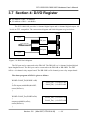
3.7
SECTION 4: D/I/O REGISTER ............................................................................................................. 61
3.8
SECTION 5: A/D & D/A REGISTER .................................................................................................... 62
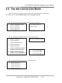
A/D CONVERSION OPERATION ............................................................................................................ 64
4.1
THE CONFIGURATION CODE TABLE .................................................................................................. 64
4.2
THE UNIPOLAR/BIPOLAR .................................................................................................................. 65
4.3
THE INPUT SIGNAL RANGE ............................................................................................................... 65
4.4
THE SETTLING TIME ......................................................................................................................... 66
4.5
HOW TO DELAY THE SETTLING TIME ................................................................................................ 66
4.6
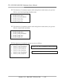
THE AD CONVERSION MODE............................................................................................................ 67
4.7
THE FIXED-CHANNEL MODE AD CONVERSION ................................................................................ 69
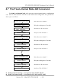
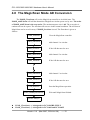
4.8
THE MAGICSCAN MODE AD CONVERSION ....................................................................................... 70
4.8.1
The MagicScan Circular_Scan_Queue............................................................................................ 71
4.8.2
The Digital Filter of MagicScan ...................................................................................................... 72
4.8.3
The Different Sampling Rate of MagicScan ..................................................................................... 72
4.8.4
The High/Low Alarm of MagicScan................................................................................................. 73
4.8.5
The MagicScan Function ................................................................................................................. 74
4.8.6
The MagicScan Thread .................................................................................................................... 76
M_FUNCTION............................................................................................................................................. 79
5.1
6.
7.
INTRODUCTION ................................................................................................................................. 80
CONTINUOUS CAPTURE FUNCTIONS ................................................................................................ 84
6.1
GENERAL PURPOSE DRIVER .............................................................................................................. 84
6.2
SAVE DATA IN PC MEMORY DRIVER ............................................................................................... 88
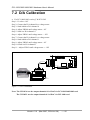
CALIBRATION ........................................................................................................................................... 90
7.1
AD CALIBRATION ............................................................................................................................. 90
7.2
D/A CALIBRATION ............................................................................................................................ 92
Version: 3.8
(Mar.2007, PPH-014-38)
---- 3
PCI-1202/1602/1800/1802 Hardware User’s Manual
8.
SOFTWARE AND DEMO PROGRAM .................................................................................................... 94
9.
DIAGNOSTIC PROGRAM ........................................................................................................................ 96
9.1
POWER-ON PLUG&PLAY TEST.......................................................................................................... 96
9.2
DRIVER PLUG&PLAY TEST ............................................................................................................... 96
9.3
D/O TEST.......................................................................................................................................... 97
9.4
D/A TEST.......................................................................................................................................... 97
9.5
A/D TEST.......................................................................................................................................... 97
10.
PERFORMANCE EVALUATION........................................................................................................ 98
Version: 3.8
(Mar.2007, PPH-014-38)
---- 4
PCI-1202/1602/1800/1802 Hardware User’s Manual
1. Introduction
1.1 General Description
The PCI-1800(H/L) and PCI-1802(H/L) are high performance, multifunction analog, digital
I/O board for PC and compatible computers in a 5V PCI slot. This series features a continuous,
330K samples/second, gap-free data acquisition under DOS, Windows 95/98 and Windows
NT 3.51/4.0. This family has the same features: one 12-bit 330K AD converter, two 12-bit
independent DA converter, 16 channels TTL compatible DI and 16 channels TTL compatible
DO. The 1800H/L provides 16 channels single-ended or 8 channel differential inputs. The
1802H/L provides 32 channels single-ended or 16 differential inputs. The letter `L' denotes
the low gain and the `H' denotes the high gain. Two DACs of this multifunction card are
independent bipolar voltage output with jumper selectable voltage output range. The AD scan
function of 1800 series is very amazing; we call it “MagicScan". It scans with two modes:
the fix channel mode and the channel scan mode, both modes can be up to 330K samples per
second. We also provide three trigger modes for this series: software trigger, pacer trigger and
external trigger; each trigger mode uses “MagicScan" to perform the data acquisition. The
external trigger can be programmed to one of the three trigger methods : pre-trigger, posttrigger and middle-trigger. The PCI-1800/1802 fully supports “ Plug and Play " under
Windows 95/98/2000/XP.
The PCI-1202HU/LU are new version of PCI-1202H/L, they can be installed in 3.3V, 5V
or 3.3V/5V Universal PCI-Bus. The PCI-1202H/L could be replaced with PCI-1202HU/LU
without modifying software.
The PCI-1202(H/L/HU/LU) is very similar to PCI-1802(H/L). The different items between the
PCI-1802 and PCI-1202 are given as follows:
z A/D sampling rate is 110K samples/second for PCI-1202(L/LU)
z FIFO size is 2K words
The PCI-1602 is very similar to PCI-1802L. The different items between the PCI-1802
and PCI-1602 are given as follows:
z A/D is 16-bit
z A/D sampling rate is 200K samples/second for PCI-1602F
z A/D sampling rate is 100K samples/second for PCI-1602
Version: 3.8
(Mar.2007, PPH-014-38)
---- 5
PCI-1202/1602/1800/1802 Hardware User’s Manual
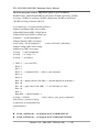
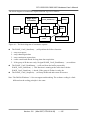
1.2 The Block Diagrams
The block diagram of PCI-1202/1602/1800/1802 is given as follows:
X86 System
PCI BUS
PCI Interface System
EPROM
Status
Control
Local System Controller
Digital Input
16 bits DI
16 bits DO
Digital Output
DAC OUT 0
2 channels
12 bit DA
Converter
DAC OUT 1
Analog Output
Magic Scan Controller
FIFO
2/8K
12/16bit A/D
Converter
Gain
Mu
x
Analog Input
Figure 1-1 The block diagram of PCI-1202/1602/1800/1802
Version: 3.8
(Mar.2007, PPH-014-38)
---- 6
PCI-1202/1602/1800/1802 Hardware User’s Manual
1.3 Features
The general features of PCI-1202/1602/1800/1802 series are given as follows:
z Bus: 5V PCI ( Peripherals Component Interface) bus.
z A/D:
1. PCI-1800(L)/1802(L) : A/D converter = 330K samples/second
PCI-1800(H)/1802(H) : A/D converter = 44K samples/second
PCI-1602F: A/D converter = 200K samples/second
PCI-1602: A/D converter = 100K samples/second
PCI-1202(L/LU): A/D converter = 110K samples/second
PCI-1202(H/HU): A/D converter = 44K samples/second
2. 32 single-ended / 16 differential analog inputs for PCI-1202/1602/1802 H/L/HU/LU.
3. Three different A/D triggers: software, pacer and external trigger
. 4. Provides three different external triggers: pre-trigger, middle-trigger and post-trigger
5. Programmable input signal configuration.
6. Provides “MagicScan” function
7. FIFO:
2K for PCI-1202(H/L/HU/LU)/1800(H/L)
8K for PCI-1802(H/L)
8K for PCI-1602, PCI-1602F and PCI-1802(H/L)
z D/A:
1. Two channels independent 12 bits DACs.
2. Bipolar voltage output with +/-5V or +/- 10V jumper selectable.
3. High throughput: refer to chapter 10.
z
DIO:
1. 16 channels TTL compatible DI and 16 channels TTL compatible DO.
2. High speed data transfer rate: refer to chapter 10.
zTimer:
1. Three 16-bits timer/counter (8254).
2. Timer 0 is used as the internal A/D pacer trigger timer.
3. Timer 1 is used as the external trigger timer.
4. Timer 2 is used as the machine independent timer for settling time delay.
Version: 3.8
(Mar.2007, PPH-014-38)
---- 7
PCI-1202/1602/1800/1802 Hardware User’s Manual
1.4 Specifications
1.4.1 Power Consumption:
z
z
+5V @960mA maximum, PCI-1202/1602/1800/1802.
Operating temperature : 0°C ~ +70°C
1.4.2 Analog Inputs
z
z
z
Channels: ( software programmable )
1. PCI-1202/1602/1802: 32-single-ended/16-differential inputs, jumper select.
2. PCI-1800: 16-single-ended/8-differential inputs, jumper select.
Gain control: ( software programmable )
1. PCI-1202/1800/1802 L/LU: 0.5, 1, 2, 4, 8.
2. PCI-1202/1800/1802 H/HU: 0.5, 1, 5, 10, 50, 100, 500, 1000.
3. PCI-1602/1602F: 1,2,4,8.
Bipolar input signal range :
1. PCI-1202/1800/1802 L/LU: ±10V,±5V, ±2.5V, ±1.25V, ±0.625V.
2. PCI-1202/1800/1802 H/HU: ±10V,±5V,±1V, ±0.5V, ±0.1V, ±0.05V, ±0.01V, ± 0.005V.
3. PCI-1602/1602F: ±10V,±5V,±2.5V,±1.25V
z
Unipolar input signal range :
1. PCI-1202/1800/1802 L/LU: 0~10V, 0~5V, 0~2.5V, 0~1.25.V.
2. PCI-1202/1800/1802 H/HU: 0~10V, 0~1V, 0~0.1V, 0~0.01V
z Input current : 250 nA max (125 nA typical ) at 25 °C.
z Over voltage : continuous single channel to 70Vp-p
z
Input impedance :
PCI-1202/1602/1800/1802 L/LU: 1013Ω // 1pF
PCI-1202/1800/1802 H/HU: 1010Ω // 6pF
Version: 3.8
(Mar.2007, PPH-014-38)
---- 8
PCI-1202/1602/1800/1802 Hardware User’s Manual
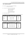
1.4.3 A/D Converter
z
Resolution: 12-bit for PCI-1202/1800/1802 H/L/HU/LU
16-bit for PCI-1602/1602F
z
z
Conversion Cycle: 330K s/s for PCI-1800/1802L
44K s/s for PCI-1800/1802H
200K s/s for PCI-1602F
100K s/s for PCI-1602
110K s/s for PCI-1202 L/LU
44K s/s for PCI-1202H/HU
Internal sample and hold.
z
12-bit ADC Input Voltages and Output Codes for PCI-1202/1800/1802 H/L/HU/LU
Analog Input
Digital Output Binary Code
MSB
+9.995V
0V
-4.88mv
-10V
•
Hex Code
LSB
1111
1000
0111
0000
1111
0000
1111
0000
1111
0000
1111
0000
FFF
800
7FF
000
16-bit ADC Input Voltages and Output Codes for PCI-1602/1602F
Analog Input
+9.99V
+0V
-305µV
-10V
Digital Output Binary Code
MSB
0111
0000
1111
1000
Hex Code
LSB
1111
0000
1111
0000
Version: 3.8
1111
0000
1111
0000
1111
0000
1111
0000
(Mar.2007, PPH-014-38)
7FFF
0000
FFFF
8000
---- 9
PCI-1202/1602/1800/1802 Hardware User’s Manual
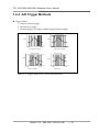
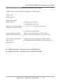
1.4.4 A/D Trigger Methods
z Trigger modes:
1. Internal software trigger
2. Internal pacer trigger
3. External trigger: pre-trigger, middle-trigger and post-trigger
External trigger
CHn
CHn
t
Start
End
Internal pacer trigger
Start
End
t
External post-trigger
External trigger
External trigger
CHn
CHn
N2
End
Start
External middle-
t
Start
End
t
External pre-
Figure 1-2 Trigger modes of PCI-1202/1602/1800/1802
Version: 3.8
(Mar.2007, PPH-014-38)
---- 10
PCI-1202/1602/1800/1802 Hardware User’s Manual
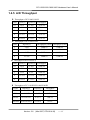
1.4.5 A/D Throughput
•
Throughput of PCI-1800L/1802L
Gains Bipolar(V) Unipolar(V) Throughput
•
0.5
±10V
0~10V
333K s/s
1
±5V
0~10V
333K s/s
2
±2.5V
0~5V
333K s/s
4
±1.25V
0~2.5V
333K s/s
8
±0.625V
0~1.25V
333K s/s
Throughput of PCI-1602F/1602
Gains
Bipolar(V)
1
±10V
200K s/s
100K s/s
2
±5V
200K s/s
100K s/s
4
±2.5V
200K s/s
100K s/s
8
±1.25V
200K s/s
100K s/s
•
Throughput (1602F) Throughput (1602)
Throughput of PCI-1202L/LU
Gains Bipolar(V) Unipolar(V) Throughput
•
0.5
±10V
0~10V
110K s/s
1
±5V
0~10V
110K s/s
2
±2.5V
0~5V
110K s/s
4
±1.25V
0~2.5V
110K s/s
8
±0.625V
0~1.25V
110K s/s
Throughput of PCI-1202H/HU/1800H/1802H
Gains
Bipolar(V)
Unipolar(V)
Throughput
0.5/1
±10/±5V
0~10V
40K s/s
5/10
±1/±0.5V
0~1V
40K s/s
50/100
±0.1/±0.05V
0~0.1V
10K s/s
0~0.01V
1K s/s
500/1000 ±0.01/±0.005V
Version: 3.8
(Mar.2007, PPH-014-38)
---- 11
PCI-1202/1602/1800/1802 Hardware User’s Manual
1.4.6 D/A Converter
z
z
z
z
Channels: 2 independent.
DAC Type: 12-bit multiplying DA converter.
Accuracy: ±1 bit.
Output type: 12-bit double buffered
z
z
z
z
Output range: -5~+5V or -10~+10V jumper select.
Output drive: ± 5mA
Settling time: 0.4 μs (typical) to 0.01% for full scale step.
Data transfer rate: 2.1M words/second (non-burst mode).
z
12- bit DAC output code for PCI-1202/1800/1802 H/L/HU/LU
Data Input
MSB
Analog Output
LSB
1111
1000
1000
0111
0000
1111
0000
0000
1111
0000
1111
0001
0000
1111
0000
Version: 3.8
+Vref (2047/2048)
+Vref (1/2048)
0 Volts
-Vref (1/2048)
-Vref (2048/2048)
(Mar.2007, PPH-014-38)
---- 12
PCI-1202/1602/1800/1802 Hardware User’s Manual
1.4.7 Digital I/O
z
z
z
Output port: 16-bit, TTL compatible
Input port: 16-bit, TTL compatible
Throughput: 2.1M word/sec ( non-burst mode ).
1.4.8 Interrupt Channel
z
z
Interrupt: Automatically assigned by ROM BIOS.
Enable/Disable: Via on-board control register.
1.4.9 Programmable Timer/Counter
z
z
Type: 82C54 programmable timer/counter
Timers: three 16-bit independent timer
1. Timer 0 is used as the internal A/D pacer trigger timer.
2. Timer 1 is used as the external trigger A/D pacer timer.
3. Timer 2 is used as the machine independent timer.
z Input clock: 8 M Hz.
Version: 3.8
(Mar.2007, PPH-014-38)
---- 13
PCI-1202/1602/1800/1802 Hardware User’s Manual
1.5 Applications
z
z
z
z
z
z
z
z
z
z
Signal analysis.
FFT & frequency analysis.
Transient analysis.
Speech analysis.
Temperature monitor.
Production test.
Process control.
Vibration analysis.
Energy management.
Other industrial and laboratory measurement and control.
1.6 Product Check List
In addition to this manual, the package includes the follows items:
z
z
PCI-1202/1602/1800/1802 H/L/HU/LU multifunction card.
One ICPDOS CD-ROM or diskette.
It’s recommended to read the release note first. All important information will be given in
release notes as follows:
1. Where you can find the software driver & utility
2. How to install software & utility
3. Where is the diagnostic program
4. FAQ
Attention !
If any of these items is missing or damaged, please contact your local agent.
Save the shipping materials and carton in case you want to ship or store the
product in the future.
Version: 3.8
(Mar.2007, PPH-014-38)
---- 14
PCI-1202/1602/1800/1802 Hardware User’s Manual
2. Hardware Configuration
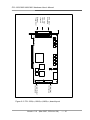
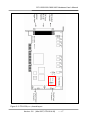
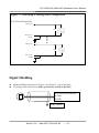
2.1 Board Layout
ADC input
16 or 32
channels
External
Trigger Input
CON3
JP1 VR1 VR100 VR101
1 2
5 6
PCI-1800/1802L/NDA REV:C
VR2
VR3
J1
10V
5V
CON2
CON1
OUT
IN
Digital Input
16 channels
Digital Output
16 channels
Figure 2-1 PCI-180X(H/L)/NDA board layout
Version: 3.8
(Mar.2007, PPH-014-38)
---- 15
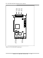
PCI-1202/1602/1800/1802 Hardware User’s Manual
DAC output
2 channels
ADC input
16 or 32
channels
External
Trigger Input
CON3
JP1
1 2
5 6
VR1 VR100 VR101
PCI-1800/1802L REV:F
VR201 VR200 VR202 VR203
VR2
J1
10V
5V
CON2
CON1
Digital Input
16 channels
Digital Output
16 channels
---- 16
(Mar.2007, PPH-014-38)
Version: 3.8
IN
OUT
Figure 2-2 PCI-1202(H/L)/1800(H/L)/1802(H/L) board layout
PCI-1202/1602/1800/1802 Hardware User’s Manual
Figure 2-3. PCI-1202(HU/LU) board layout
Version: 3.8
(Mar.2007, PPH-014-38)
---- 17
PCI-1202/1602/1800/1802 Hardware User’s Manual
CON3
VR1
6
2
JP1
5
VR2 VR3
VR4
VR5 VR6
VR7
J1
10V
5V
CON2
DAC output
2 channels
CON1
1
ADC input
32 channels
External
Trigger Input
PCI-1602/1602F REV:1.0
Digital Input
16 channels
Digital Output
16 channels
---- 18
(Mar.2007, PPH-014-38)
Version: 3.8
IN
OUT
Figure 2-4 PCI-1602/1602F board layout
PCI-1202/1602/1800/1802 Hardware User’s Manual
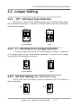
2.2 Jumper Setting
2.2.1
JP1 : A/D Input Type Selection
This jumper is used to select the analog input type. For single-ended inputs,
the use should connect pin1, 3 and pin2, 4. For differential inputs, pin3, 5 and pin4,
6 should be connected.
JP1
JP1
1
2
5
6
1
2
5
6
Differential
Inputs
Single-Ended
Inputs (default)
2.2.2 J1 : D/A Reference Voltage Selection
J1 is used to select the internal D/A output reference voltage. To select the
±10V voltage output, the pin 1&2 should be connected. To select the ±5V voltage
output, the pin 2&3 should be connected.
J1
J1
1
1
± 5 Voltage
output
± 10 Voltage
output (default)
2.2.3
D/I Port Setting (PCI-1202HU/LU only)
This DI ports can be pull-high or pull-low selected by JP2. The location is
given as following:
JP2
3
2
1
Pull High
Version: 3.8
3
2
1
JP2
Pull Low
(Mar.2007, PPH-014-38)
---- 19
PCI-1202/1602/1800/1802 Hardware User’s Manual
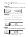
2.3 Daughter Boards
2.3.1 DB-1825
The DB-1825 is a daughter board designed for 32 channels AD cards such as ISO_AD32,
PCI-1202/1602/1802. Refer to Appendix A for “DB-1825 user manual".
37pin cable
2.3.2 DB-8225
The DB-8225 provides a on-board CJC(Cold Junction Compensation) circuit for
thermocouple measurement and terminal block for easy signal connection and measurement.
The CJC is connected to A/D channel_0. The PCI-1800 can connect CON3 direct to DB-8225
through a 37-pin D-sub connector. Refer to “DB-8225 User Manual" for details.
2.3.3 DB37
The DB-37 is a general purpose daughter board for D-sub 37 pins. It is designed for easy
wire connection.
2.3.4 DN37
The DN-37 is a general purpose daughter board for DIN Rail Mounting. It is designed for
easy wire connection. It is Din-Rail mounting.
37pin cable
Version: 3.8
(Mar.2007, PPH-014-38)
---- 20
PCI-1202/1602/1800/1802 Hardware User’s Manual
2.3.5 DB-16P Isolated Input Board
The DB-16P is a 16-channel isolated digital input daughter board. The optically isolated
inputs of the DB-16P consists are bi-directional optocoupler with resistor for current sensing.
You can use the DB-16P to sense DC signal from TTL levels up to 24V or use the DB-16P to
sense a wide range of AC signals. You can use this board to isolate the computer from large
common-mode voltage, ground loops and transient voltage spike that often occur in industrial
environments.
Opto-Isolated
R
PCI-1202 (H/L/HU/LU)
PCI-1800/1802 (H/L)
D/I
V+
D/I
V-
20-Pin cable
DB-16P
PCI-1202 (H/L/HU/LU)
PCI-1800/1802 (H/L)
AC or DC Signal 0V to 24V
Version: 3.8
(Mar.2007, PPH-014-38)
---- 21
PCI-1202/1602/1800/1802 Hardware User’s Manual
2.3.6 DB-16R Relay Board
The DB-16R, 16-channel relay output board, consists of 16 from C relays for efficient
switch of load by programmed control. It is connector and functionally compatible with 785
series board but with industrial type terminal block. The relay are energized by apply 5 voltage
signal to the appropriated relay channel on the 20-pin flat connector. There are 16 enunciator
LEDs for each relay, light when their associated relay is activated. To avoid overloading your
PC's power supply, this board provides a screw terminal for external power supply.
From C Relay
Normal Open
Normal Close
Com
D/O
PCI-1202 (H/L/HU/LU)
PCI-1800/1802(H/L)
20-Pin cable
DB-16R
Note: Channel: 16 From C Relay
Relay: Switching up to 0.5A at 110ACV or 1A at 24 DCV
Version: 3.8
(Mar.2007, PPH-014-38)
---- 22
PCI-1202/1602/1800/1802 Hardware User’s Manual
2.3.7 DB-24PR Power Relay Board
The DB-24PR, 24-channel power relay output board, consists of 8 form C and 16 form A
electromechanical relays for efficient switching of load programmed control. The contact of
each relay can control a 5A load at 250ACV/30VDCV. The relay is energized by applying a 5
voltage signal to the appropriate relay channel on the 20-pin flat cable connector (just used 16
relays) or 50-pin flat cable connector. (OPTO-22 compatible, for DIO-24 series). Twenty - four
enunciator LEDs, one for each relay, light when their associated relay is activated. To avoid
overloading your PC's power supply, this board needs a +12VDC or +24VDC external power
supply.
Normal Open
From C Relay
Normal Close
Com
D/O
PCI-1202 (H/L/HU/LU)
PCI-1800/1802 (H/L)
20-Pin cable
DB-24PR
Note: 50-Pin connector (OPTO-22 compatible), for DIO-24, DIO-48, DIO-144
20-Pin connector for 16 channel digital output, A-82X, A-62X, DIO-64, ISO-DA16/DA8
Channel: 16 From A Relay , 8 From C Relay
Relay: Switching up to 5A at 110ACV / 5A at 30DCV
Version: 3.8
(Mar.2007, PPH-014-38)
---- 23
PCI-1202/1602/1800/1802 Hardware User’s Manual
2.4 Analog Input Signal Connection
The PCI-1202/1602/1800/1802 can measure single-ended or differential type analog input
signal. Some analog signal can be measured in single-end or differential mode, but some
analog signal only can be measured in one of the single-ended or differential mode. The user
must decide which mode is suitable for measurement.
In general, there are 4 different analog signal connection methods as shown in Figure 2-4
to Figure 2-7. The Figure 2-4 is suitable for grounding source analog input signals. The Figure
2-5 is used to measure more channels than in the Figure 2-4 but only suitable for large analog
input signals. The Figure 2-6 is suitable for thermocouple and the Figure 2-7 is suitable for
floating source analog input signals. Note : In Figure 2-6, the maximum common mode
voltage between the analog input source and the AGND is 70Vp-p, so the user must take
care that the input signal is under specification first. If the common mode voltage is over
70Vp-p, the input multiplexer will be damaged forever.
The simple way to select the input signal connection configuration is as below.
1. Grounding source input signal Æ select Figure 2-4
2. Thermocouple input signal
Æ select Figure 2-6
3. Floating source input signal
Æ select Figure 2-7
4. If Vin > 0.1V and gain<=10 and need more channels
Æ select Figure 2-5
If the user can not make sure the characteristic of input signal, the test steps are given as below:
1.
2.
3.
4.
Step1 : try Figure 2-4 and record the measurement result
Step2 : try Figure 2-7 and record the measurement result
Step3 : try Figure 2-5 and record the measurement result
Compare the measurement result of step1,step2,step3 and select
the best one
Version: 3.8
(Mar.2007, PPH-014-38)
---- 24
PCI-1202/1602/1800/1802 Hardware User’s Manual
Figure 2-4. Connecting to grounding source input (Right way)
A/D CH0 HI
Es 1
A/D CH 0 LO
A.GND 1
A/D CH n HI
Es n
A/D CHn LO
A.GND n
Figure 2-4. Wrong way
A/D CH0HI
Es1
A/D CH0LO
AGND
GND1
A/D CHnHI
Esn
A/D CHnLO
GNDn
AGND
Version: 3.8
(Mar.2007, PPH-014-38)
---- 25
PCI-1202/1602/1800/1802 Hardware User’s Manual
Figure 2-5. Connecting to singled-ended input configuration
PCI-1202/1602/1800/1802
A/D CH0
A/D CH1
A/D CH n
Es
AGND
Figure 2-6. connecting to thermocouple configuration
PCI-1202/1602/1800/1802
A/D CH 0 HI
A/D CH 0 LO
A/D CH n HI
A/D CH n LO
A. GND
Do not join LO to A.GND at the computer
Note : If the input signal is not thermocouple, the user should use oscilloscope to measure
common mode voltage of Vin before connecting to PCI-1202/1602/1800/1802. Don't use
voltage meter or multimeter.
CAUTION: In Figure 2-6, the maximum common mode voltage between
the analog input source and the AGND is 70Vp-p, so the user must make sure that the input
signal is under specification first. If the common mode voltage is over 70Vp-p, the input
multiplexer will be damaged forever.
Version: 3.8
(Mar.2007, PPH-014-38)
---- 26
PCI-1202/1602/1800/1802 Hardware User’s Manual
Figure 2-7. connecting to floating source configuration
PCI-1202/1602/1800/1802
A/D CH 0 HI
Es 1
A/D CH 0 LO
A.GND
A/D CH n HI
Es n
A/D CH n LO
A.GND
Signal Shielding
z
z
Signal shielding connections in Figure 2-4 to Figure 2-7 are all the same
Use single-point connection to frame ground (not A.GND or D.GND)
PCI-1202/1602/1800/1802
A.GND
D.GND
Vin
Frame Ground
Version: 3.8
(Mar.2007, PPH-014-38)
---- 27
PCI-1202/1602/1800/1802 Hardware User’s Manual
2.5 The Connectors
CON1: Pin assignment of the digital output connector.
Pin
Name
Pin
Name
1
Digital output 0
2
Digital output 1
3
Digital output 2
4
Digital output 3
5
Digital output 4
6
Digital output 5
17
Digital output 6
8
Digital output 7
9
Digital output 8
10
Digital output 9
11
Digital output 10
12
Digital output 11
13
Digital output 12
14
Digital output 13
15
Digital output 14
16
Digital output 15
17
PCB ground
18
PCB ground
19
PCB +5V
20
PCB +12V
CON2: Pin assignment of digital input connector.
Pin
Name
Pin
Name
1
Digital input 0
2
Digital input 1
3
Digital input 2
4
Digital input 3
5
Digital input 4
6
Digital input 5
7
Digital input 6
8
Digital input 7
9
Digital input 8
10
Digital input 9
11
Digital input 10
12
Digital input 11
13
Digital input 12
14
Digital input 13
15
Digital input 14
16
Digital input 15
17
PCB ground
18
PCB ground
19
PCB +5V
20
PCB +12V
Version: 3.8
(Mar.2007, PPH-014-38)
---- 28
PCI-1202/1602/1800/1802 Hardware User’s Manual
C0N3: pin assignment of single-ended/differential input.
(for PCI-1202/1602/1802H/L/HU/LU)
Pin
Name
Pin
Name
1
Analog input 0/0+
20
Analog input 16/0-
2
Analog input 1/1+
21
Analog input 17/1-
3
Analog input 2/2+
22
Analog input 18/2-
4
Analog input 3/3+
23
Analog input 19/3-
5
Analog input 4/4+
24
Analog input 20/4-
6
Analog input 5/5+
25
Analog input 21/5-
7
Analog input 6/6+
26
Analog input 22/6-
8
Analog input 7/7+
27
Analog input 23/7-
9
Analog input 8/8+
28
Analog input 24/8-
10
Analog input 9/9+
29
Analog input 25/9-
11
Analog input
10/10+
30
Analog input 26/10-
12
Analog input
11/11+
31
Analog input 27/11-
13
Analog input
12/12+
32
Analog input 28/12-
14
Analog input
13/13+
33
Analog input 29/13-
15
Analog input
14/14+
34
Analog input 30/14-
16
Analog input
15/15+
35
Analog input 31/15-
17
Analog ground
36
Analog output 1
18
Analog output 0
37
Digital ground
19
External trigger
Version: 3.8
(Mar.2007, PPH-014-38)
---- 29
PCI-1202/1602/1800/1802 Hardware User’s Manual
CON3: pin assignment of single-ended/differential input.(for PCI-1800H/L)
Pin
Name
Pin
Name
1
Analog input 0/0+
20
Analog input 8/0-
2
Analog input 1/1+
21
Analog input 9/1-
3
Analog input 2/2+
22
Analog input 10/2-
4
Analog input 3/3+
23
Analog input 11/3-
5
Analog input 4/4+
24
Analog input 12/4-
6
Analog input 5/5+
25
Analog input 13/5-
7
Analog input 6/6+
26
Analog input 14/6-
8
Analog input 7/7+
27
Analog input 15/7-
9
Analog Ground
28
Analog Ground
10
Analog Ground
29
Analog Ground
11
N.C.
30
Analog output 0
12
N.C.
31
N.C.
13
PCB +12V
32
Analog output 1
14
Analog Ground
33
N.C.
15
Digital Ground
34
N.C.
16
N.C.
35
N.C.
17
External Trigger
36
N.C.
18
N.C.
37
N.C.
19
PCB +5V
N. C. : Abbreviation of “ Not Connected “.
Version: 3.8
(Mar.2007, PPH-014-38)
---- 30
PCI-1202/1602/1800/1802 Hardware User’s Manual
3. I/O Control Register
3.1 How to Find the I/O Address
The plug&play BIOS will assign a proper I/O address to every PCI-1800/1802 card in the
power-on stage. The P180X_DriverInit(..) can detect how many PCI-1800/1802 cards in the
system. Then the P180X_DriverInit(..) will detect the I/O address of these cards. The
P180X_DriverInit(..) is supported in NAPPCI/dos, NAPPCI/w31, NAPPCI/w95 and
NAPPCI/wnt. The P180X_DriverInit(..) is implemented based on the PCI plug&play
mechanism-2. The P180X_DriverInit(..) must be called once before all the other driver is
called. The function of P180X_DriverInit(..) are given as follows:
1. Detect how many PCI-1800/1802 cards in the system ?
2. Detect and save the I/O control address of every PCI-1800/1802 card
The sample program source is given as follows:
wRetVal=P180X_DriverInit(&wBoards); /* call P180X_DriverInit(..) first */
printf("Threr are %d P180X Cards in this PC\n",wBoards);
/* dump every P180X card's configuration address space */
printf("The Configuration Space -> Timer Control DIO AD/DA \n");
for (i=0; i<wBoards; i++)
{
printf("Card %02d: %04xH %04xH %04xH %04xH\n", i,wConfigSpace[i][0],
wConfigSpace[i][1], wConfigSpace[i][2],wConfigSpace[i][3]);
}
/* The P180X_ActiveBoard() function must be used to active a board, */
/* then all operation will take effect to the active board. */
printf("Now Active First P180X Card...\n");
P180X_ActiveBoard( 0 );
z P1202_DriverInit(…) is designed for PCI-1202H/L/HU/LU
z P1602_DriverInit(…) is designed for PCI-1602 and PCI-1602F
Version: 3.8
(Mar.2007, PPH-014-38)
---- 31
PCI-1202/1602/1800/1802 Hardware User’s Manual
3.2 The Assignment of I/O Address
The plug&play BIOS will assign the proper I/O address to PCI-1202/1602/1800/1802. If
there is only one PCI-1202/1602/1800/1802, the user can identify the board_1. If there are
two PCI-1202/1602/1800/1802 cards in the system, the user will be very difficult to identify
which board is board_1. The software driver can support 16 boards max. Therefore the user
can install 16 boards in one PC system.
The simplest way to find the board number is to use DEMO15.EXE given in DOS
demo program. This demo program will send to D/O and read back from D/I. If the user
installs a 20-pin flat cable between CON1 & CON2, the value read from D/I will be the same
as D/O. The operation steps are given as follows:
1. Remove all 20-pin flat cable between CON1 and CON2
2. Install all PCI-1202/1602/1800/1802 cards into the PC system
3. Power-on and run DEMO15.EXE
4. Now all D/I value will be different from D/O value
5. Install a 20-pin flat cable into CON1 & CON2 of any PCI-1202/1602/1800/1802 card
6. There will be one card' s D/I value = D/O value, the card number is also shown in
screen
Therefore the user can find the card number very easy if he install a 20-pin flat cable
into PCI-1202/1602/1800/1802 one-by-one.
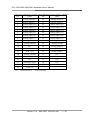
3.3 The I/O Address Map
The I/O address of PCI-1202/1602/1800/1802 is automatically assigned by the
main board ROM BIOS. The I/O address can also be reassigned by user. It is strongly
recommended not to change the I/O address by user. The plug&play BIOS will
assign proper I/O address to each PCI-1202/1602/1800/1802 very well. There are
five sections of I/O address used by this card and each section can be assigned to an
unused I/O space. The hardware I/O ports are described as follows:
Version: 3.8
(Mar.2007, PPH-014-38)
---- 32
PCI-1202/1602/1800/1802 Hardware User’s Manual
Section
1
2
3
4
5
Address
Name
Operation
Access
Section1 + 0h
PCI controller add-on
mail box
W
32-bits
Section1 + 38h
PCI interrupt control
register
R/W
32bits
Section1 + 3Ch On board NV-RAM
(or 3Eh, 3Fh) access control register
R/W
32 bits
(8 bits)
Section2 + 00h
8254 timer1
R/W
8/16/32 bits
Section2 + 04h
8254 timer2
R/W
8/16/32 bits
Section2 + 08h
8254 timer3
R/W
8/16/32 bits
Section2 + 0Ch
8254 control
W
8/16/32 bits
Section3 +00h
Control register
W
16/32 bits
Section3 + 00h
Status register
R
8/16/32 bits
Section3 + 04h
A/D software trigger
W
8/16/32 bits
Section4 + 00h
DI port
R
16 bits
Section4 + 00h
DO port
W
16 bits
Section5 + 00h
A/D data port
R
16 bits
Section5 + 00h
D/A channel 1.
W
16 bits
Section5 + 04h
D/A channel 2.
W
16 bits
The driver name of these address are given as follows:
section_2 : wAddrTimer
section_3 : wAddrCtrl
section_4 : wAddrDio
section_5 : wAddrAdda
Version: 3.8
Æ save in wConfigSpace[Board][0]
Æ save in wConfigSpace[Board][1]
Æ save in wConfigSpace[Board][2]
Æ save in wConfigSpace[Board][3]
(Mar.2007, PPH-014-38)
---- 33
PCI-1202/1602/1800/1802 Hardware User’s Manual
3.4 Section 1: PCI Controller
Although 64 I/O ports are used by on-board PCI-controller, only 3 registers can be
directly used by user.
Address
Access
Functions
Operation
Write only
(32 bit)
Out-going mail-box
+0
Write a 0 to wait for add-on
interrupt.
1.
Write
(32bit)
+38
Enable/Re-enable/
2.
Disable target interrupt
3.
Read (32bit) Read interrupt status.
Write
(8bit)
+3F
(8bits)
+3C
(32bit)
Read
(8bit)
Write command to
nvRAM control register
Enable : Write 00010010h to
this port.
Re-enable: Write 00010010h
to this port.
Disable : Write 0 to this port.
Bit 16 : 1 Æ interrupt generated.
0 Æ no interrupt.
0x80 :
0xA0:
0xC0:
0xE0:
load low address
load high address
begin write.
begin read.
Read status from
Bit 7 : 1 Æ busy
nvRAM control register
0 Æ ready
Write
(8bit)
Write nvRAM address or After finish writing to nvRAM
nvRAM data to register. control register, write data to this
port.
Read
(8bit)
Read nvRAM data from After finish writing to nvRAM
this register.
control register, read data from
this port..
+3E
(8bits)
The user does not have to know about these registers in the normal condition. Refer to
“AMCC S5933 PCI Controllers User Manual" for all registers details.
Version: 3.8
(Mar.2007, PPH-014-38)
---- 34
PCI-1202/1602/1800/1802 Hardware User’s Manual
3.5 Section 2: Timer Control
The timer-0 is used as the internal trigger A/D pacer timer. The timer-1 is designed for the
external trigger pacer timer. The timer-2 is used as the machine independent timer. The timer2 is very important for settling time delay. Refer to Intel's “Microsystem Components
Handbook" for 8254 programming. The block diagram of the 8254 timer is given as follows:
8Mhz
CLK
Timer 0
OUT0
Local Data Bus
Internal Pacer timer
ADC
CLK
Timer 1
OUT1
D0,D1 ... D7
External Pacer timer
CLK
Timer 2
OUT2
Machine indenpedent Timer
Figure 3-1: The block diagram of PCI-1202/1602/1800/1802 8254 timer.
The I/O address of 8254 timer is given as follows:
z I/O address of timer/counter_0 = wAddrTimer+0*4
z I/O address of timer/counter_1 = wAddrTimer+1*4
z I/O address of timer/counter_2 = wAddrTimer+2*4
z I/O address of control register = wAddrTimer+3*4
Version: 3.8
(Mar.2007, PPH-014-38)
---- 35
PCI-1202/1602/1800/1802 Hardware User’s Manual
// timer0 Æ for pacer trigger
void enable_timer0(WORD divv) // for internal pacer trigger
{
outport((WORD)(wAddrTimer+3*4), 0x34); /* enable pacer timer_0 */
outport((WORD)(wAddrTimer+0*4), (WORD)(divv & 0xff));
outport((WORD)(wAddrTimer+0*4), (WORD)((divv>>8) & 0xff));
}
void disable_timer0(void)
{
outport((WORD)(wAddrTimer+3*4), 0x34); /* disable pacer timer_0 */
outport((WORD)(wAddrTimer+0*4), 0x01);
outport((WORD)(wAddrTimer+0*4), 0x00);
}
// timer1 Æ for external trigger
void enable_timer1(WORD divv)
/* for external trigger pacer timer */
{
outport((WORD)(wAddrTimer+3*4), 0x74); /* enable pacer timer_1 */
outport((WORD)(wAddrTimer+1*4), (WORD)(divv & 0xff));
outport((WORD)(wAddrTimer+1*4), (WORD)((divv>>8) & 0xff));
}
void disable_timer1(void)
{
outport((WORD)(wAddrTimer+3*4), 0x74); /* disable timer_1 */
outport((WORD)(wAddrTimer+1*4), 0x01);
outport((WORD)(wAddrTimer+1*4), 0x00);
}
Version: 3.8
(Mar.2007, PPH-014-38)
---- 36
PCI-1202/1602/1800/1802 Hardware User’s Manual
// timer2 Æ for Machine Independent Timer
/* address of timer 2 = wAddrTimer+2*4
address of ctrl
= wAddrTimer+3*4
input clock
= 8M
down count 8 time = 1 us
down count 65536/8 = 8192 uS --> max 8191 uS
*/
WORD P180X_DelayUs(WORD wDelayUs)
{
WORD wDownCount,wLow,wHigh,wVal;
double fTimeOut;
if (wDelayUs>=8191) return(InvalidateDelay);
wDownCount=wDelayUs*8;
wLow=wDownCount&0xff;
wHigh=(wDownCount>>8)&0xff;
outport((wAddrTimer+3*4), 0xb0);
/* timer_2 mode_0 0xb0 */
outport((wAddrTimer+2*4), wLow);
outport((wAddrTimer+2*4), wHigh);
fTimeOut=1.0; // wait 1 to stop
for (;;)
{
wVal=inport(wAddrCtrl)&0x01;
if (wVal!=0) return(NoError);
fTimeOut+=1.0;
if (fTimeOut>6553500.0)
return(DelayTimeOut);
}
}
/* if the timer is up, this bit will be 1 */
z P1202_DelayUs(…) is designed for PCI-1202H/L/HU/LU
z P1602_DelayUs(…) is designed for PCI-1602 and PCI-1602F
Version: 3.8
(Mar.2007, PPH-014-38)
---- 37
PCI-1202/1602/1800/1802 Hardware User’s Manual
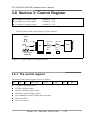
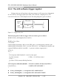
3.6 Section 3: Control Register
z I/O address of control register
z I/O address of status register
z I/O address of trigger register
= wAddrCtrl + 0*4
= wAddrCtrl + 0*4
= wAddrCtrl + 1*4
The flow path of analog input signal is given as follows:
Signals
Max=+/-10V
MUX
Single-ended
Differential
AMP1
4,3,2,1,0
Max=+/-5V
ADC
AMP1
Gain
Rang
7,6
9,8
0
1
0
:
:
:
:
.
1
Figure 3-2: The flow path of Analog input signal.
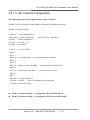
3.6.1 The control register
The format of the control register is given as follows:
B15
z
z
z
z
z
z
z
B14
B13
B12 ~ B10
B9, B8
B7, B6
B5
B4~ B0: A/D channel select
B7, B6: A/D gain control.
B9, B8: A/D input range control.
B12~B10: external trigger control.
B13: handshake control to MagicScan controller.
B15: clear FIFO.
B5, B14: reserved
Version: 3.8
(Mar.2007, PPH-014-38)
---- 38
B4 ~ B0
PCI-1202/1602/1800/1802 Hardware User’s Manual
3.6.1.1 Bit4~ Bit0: A/D channel select
A/D channel
B4
B3
B2
B1
B0
0
0
0
0
0
0
1800/1202/1602/1802
15
0
1
1
1
1
1800/1202/1602/1802
16
1
0
0
0
0
1202/1602/1802
31
1
1
1
1
1
1202/1602/1802
3.6.1.2 Gain control
[B7, B6]
PCI-1XXX L/LU PCI-1XXX H/HU
[0, 0]
PGA=1
PGA=1
[0, 1]
PGA=2
PGA=10
[1, 0]
PGA=4
PGA=100
[1, 1]
PGA=8
PGA=1000
3.6.1.3 Input range control
[B9, B8]
Output
[0, 0]
PGA
[1, 0]
PGA-5
[0, 1]
PGA/2
[1, 1]
PGA/2 - 5
Version: 3.8
(Mar.2007, PPH-014-38)
---- 39
PCI-1202/1602/1800/1802 Hardware User’s Manual
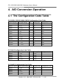
3.6.1.4 Configuration Table
The configuration table of PCI-1202L/LU/1800L/1802L is given as follows:
Bipolar/Unipolar Input Signal Range
Gain
Settling Time
[B9,B8,B7,B6]
Bipolar
+/- 5V
1
3 us
0000
Bipolar
+/- 2.5V
2
3 us
0001
Bipolar
+/- 1.25V
4
3 us
0010
Bipolar
+/- 0.625V
8
3 us
0011
Bipolar
+/- 10V
0.5
3 us
0100
Bipolar
+/- 5V
1
3 us
0101
Bipolar
+/- 2.5V
2
3 us
0110
Bipolar
+/- 1.25V
4
3 us
0111
Unipolar
0V ~ 10V
1
3 us
1000
Unipolar
0V ~ 5V
2
3 us
1001
Unipolar
0V ~ 2.5V
4
3 us
1010
Unipolar
0V ~ 1.25V
8
3 us
1011
The configuration table of PCI-1202H/HU/1800H/1802H is given as follows:
Bipolar/Unipolar Input Signal Range
Gain
Settling Time
[B9,B8,B7,B6]
Bipolar
+/- 5V
1
23 us
0000
Bipolar
+/- 0.5V
10
28 us
0001
Bipolar
+/- 0.05V
100
140 us
0010
Bipolar
+/- 0.005V
1000
1300 us
0011
Bipolar
+/- 10V
0.5
23 us
0100
Bipolar
+/- 1V
5
28 us
0101
Bipolar
+/- 0.1V
50
140 us
0110
Bipolar
+/- 0.01V
500
1300 us
0111
Unipolar
0V ~ 10V
1
23 us
1000
Unipolar
0V ~ 1V
10
28 us
1001
Unipolar
0V ~ 0.1V
100
140 us
1010
Unipolar
0V ~ 0.01V
1000
1300 us
1011
Version: 3.8
(Mar.2007, PPH-014-38)
---- 40
PCI-1202/1602/1800/1802 Hardware User’s Manual
3.6.1.5 Set Channel Configuration
The demo program to set the channel/gain is given as follows:
WORD P180X_SetChannelConfig(WORD wAdChannel, WORD wAdConfig)
{
WORD wConfig,wChannel;
wChannel = (wAdChannel&0x1f);
wSysConfig = (wAdConfig&0x1f);
wConfig = (wAdConfig&0x0f);
wConfig = wConfig << 6;
wConfig += wChannel;
// store for P1802_AdPolling
/* Bit15=1 --> no reset FIFO
Bit14=?
Bit13=?
Bit12=0 --> command [001] --> set channel&Config command
Bit11=0
Bit10=1
Bit9 =B --> Range control code [BB] --> unipolar/bipolar & divided by 2
Bit8 =B
Bit7 =B --> gain control code [BB] --> 1/10/100/1000 or 1/2/4/8
Bit6 =B
Bit5 =?
Bit4-Bit0 --> channel number */
wConfig+= 0x8400; // this is set channel config command
return(pic_control(wConfig));
}
z
z
P1202_SetChannelConfig(…) is designed for PCI-1202H/L/HU/LU
P1602_SetChannelConfig(…) is designed for PCI-1602 and PCI-1602F
Version: 3.8
(Mar.2007, PPH-014-38)
---- 41
PCI-1202/1602/1800/1802 Hardware User’s Manual
3.6.1.6 Calculate the A/D Value
The demo program to calculate the real A/D value is given as follows:
double ComputeRealValue(DWORD dwAdConfig, DWORD dwAdHex)
{
WORD wZERO;
double dfMAX, dfVal;
switch (dwAdConfig)
{ case 0 : wZERO=2048; dfMAX=5.0; break;
case 1 : wZERO=2048; dfMAX=2.5; break;
case 2 : wZERO=2048; dfMAX=1.25; break;
case 3 : wZERO=2048; dfMAX=0.625; break;
case 4 : wZERO=2048; dfMAX=10.0; break;
For PCI-1202/1800/1802L
case 5 : wZERO=2048; dfMAX=5.0; break;
case 6 : wZERO=2048; dfMAX=2.5; break;
case 7 : wZERO=2048; dfMAX=1.25; break ;
Note: B4=0 is used
case 8 : wZERO= 0; dfMAX=10.0/2.0; break;
to identify PGL
case 9 : wZERO= 0; dfMAX=5.0/2.0;
break;
case 10: wZERO= 0; dfMAX=2.5/2.0;
break;
case 11: wZERO= 0; dfMAX=1.25/2.0; break;
case 0x10 : wZERO=2048; dfMAX=5.0;
break;
case 0x11 : wZERO=2048; dfMAX=0.5;
break;
case 0x12 : wZERO=2048; dfMAX=0.05; break;
case 0x13 : wZERO=2048; dfMAX=0.005; break;
case 0x14 : wZERO=2048; dfMAX=10.0; break;
case 0x15 : wZERO=2048; dfMAX=1.0;
break ;
For PCIcase 0x16 : wZERO=2048; dfMAX=0.1;
break;
1202/1800/1802H
case 0x17 : wZERO=2048; dfMAX=0.01; break;
case 0x18 : wZERO= 0; dfMAX=10.0/2.0; break ;
Note: B4=1 is used to
case 0x19 : wZERO= 0; dfMAX=1.0/2.0; break;
identify PGH
case 0x1A : wZERO= 0; dfMAX=0.1/2.0; break;
case 0x1B : wZERO= 0; dfMAX=0.01/2.0; break;
default: return(ConfigCodeError); }
dfVal=(((double)(wAdHex)-wZERO)/2048.0)*dfMAX;
return(dfVal);
}
Version: 3.8
(Mar.2007, PPH-014-38)
---- 42
PCI-1202/1602/1800/1802 Hardware User’s Manual
3.6.1.7 Command Sets of MagicScan Controller
The command sets of MagicScan controller are given as follows:
Command
Reset
[B12~B10]
Descriptions
[0 0 0]
Reset the MagicScan controller. The software driver
must send this command once after power-on.
Set channel/gain
[0 0 1]
Set the channel/gain value of the fixed-channel mode. It
will not affect the scan queue.
Add to scan queue
[1 0 0]
Add the channel/gain code to the scan queue.
(At most 48 scan-channels can be stored in the
MagicScan controller.)
Start MagicScan
[1 0 1]
Start the MagicScan controller
Stop MagicScan
[0 1 0]
Stop the MagicScan controller.
Get ODM number
[1 1 0]
Get the ODM number of the PCI-1202/1602/1800/1802.
The demo program to reset the MagicScan controller is given as follows:
wVal=pic_control(0xC000);
/* 11?0 00?? ???? ???? cmd_000=reset */
The demo program to clear MagicScan queue is given as follows:
WORD P180X_ClearScan(void)
{
WORD i;
for(i=0; i<32; i++) wMagicScanSave[i]=0;
disable_timer0();
disable_timer1();
return(pic_control(0xC000));
/* 11?0 00?? ???? ???? cmd_000=reset */
}
z
z
P1202_ClearScan(…) is designed for PCI-1202H/L/HU/LU
P1602_ClearScan(…) is designed for PCI-1602 and PCI-1602F
Version: 3.8
(Mar.2007, PPH-014-38)
---- 43
PCI-1202/1602/1800/1802 Hardware User’s Manual
The demo program of send command to MagicScan control is given as follows:
WORD pic_control(WORD i)
{
WORD j;
if ((inport(wAddrCtrl)&0x04)==0)
{
outport(wAddrCtrl,0xffff);
}
/* send a recovery to PIC */
j=0;
while ((inport(wAddrCtrl)&0x04)==0)
{
j++;
if (j>65530) return(AdControllerError); /* time out */
}
i = i & 0xDFFF;
outport(wAddrCtrl,i);
/* set pic low !! */
j=0;
while ((inport(wAddrCtrl)&0x04)!=0)
{
j++;
if (j>65530) return(AdControllerError); /* time out */
}
outport(wAddrCtrl,(WORD)(i | 0x2000)); /* set pic high !! */
j=0;
while ((inport(wAddrCtrl)&0x04)==0)
{
j++;
if (j>65530) return(AdControllerError); /* time out */
}
return(NoError);
}
Version: 3.8
(Mar.2007, PPH-014-38)
---- 44
PCI-1202/1602/1800/1802 Hardware User’s Manual
The demo program to set the channel/gain is given as follows:
WORD P180X_SetChannelConfig(WORD wAdChannel, WORD wAdConfig)
{
WORD wConfig,wChannel;
wChannel = (wAdChannel&0x1f);
wSysConfig = (wAdConfig&0x1f);
wConfig = (wAdConfig&0x0f);
wConfig = wConfig << 6;
wConfig += wChannel;
// store for P1802_AdPolling
/* Bit15=1 --> no reset FIFO
Bit14=?
Bit13=?
Bit12=0 --> command [001] --> set channel&Config command
Bit11=0
Bit10=1
Bit9 =B --> Range control code [BB] --> unipolar/bipolar & divided by 2
Bit8 =B
Bit7 =B --> gain control code [BB] --> 1/10/100/1000 or 1/2/4/8
Bit6 =B
Bit5 =?
Bit4-Bit0 --> channel number */
wConfig+= 0x8400; // this is set channel config command
return(pic_control(wConfig));
}
z
z
P1202_SetChannelConfig(…) is designed for PCI-1202H/L/HU/LU
P1602_SetChannelConfig(…) is designed for PCI-1602 and PCI-1602F
Version: 3.8
(Mar.2007, PPH-014-38)
---- 45
PCI-1202/1602/1800/1802 Hardware User’s Manual
The demo program to add to MagicScan queue is given as follows:
WORD P180X_AddToScan(WORD wAdChannel, WORD wAdConfig, WORD
wAverage, WORD wLowAlarm, WORD wHighAlarm, WORD wAlarmType)
{WORD wConfig,wChannel,wRetVal;
if (wAlarmType>=5) return(AlarmTypeError);
wMagicLowAlarm[wMP]=wLowAlarm;
wMagicHighAlarm[wMP]=wHighAlarm;
wMagicAlarmType[wMP]=wAlarmType;
wChannel = wAdChannel&0x1f;
wMagicChannel[wMP]=wChannel;
wSysConfig = wAdConfig&0x1f;
/* Store for P180X_AdPolling */
wMagicConfig[wMP]=wSysConfig;
wMagicAve[wMP]=wAverage;
wConfig = wAdConfig&0x0f;
wConfig = wConfig << 6;
wConfig += wChannel;
/* Bit15=1 --> no reset FIFO
Bit14=1
Bit13=?
Bit12=1 --> command [100] --> add_to_scan command
Bit11=0
Bit10=0
Bit9 =B --> Range control code [BB] --> unipolar/bipolar & divided by 2
Bit8 =B
Bit7 =B --> gain control code [BB] --> 1/10/100/1000 or 1/2/4/8
Bit6 =B
Bit5 =?
Bit4-Bit0 --> channel number */
wConfig+= 0xD000;
/* this is add_to_scan_queue command */
wRetVal=pic_control(wConfig);
if (wRetVal!=0) return(wRetVal);
return(NoError);
}
z
z
P1202_AddToScan(…) is designed for PCI-1202H/L/HU/LU
P1602_AddToScan(…) is designed for PCI-1602 and PCI-1602F
Version: 3.8
(Mar.2007, PPH-014-38)
---- 46
PCI-1202/1602/1800/1802 Hardware User’s Manual
The demo program to start MagicScan operation is given as follows:
WORD P180X_StartScan(WORD wSampleRate, WORD wNum)
{
WORD wVal;
WORD wRetVal;
wMagicNum=wNum;
disable_timer0();
/* Disable pacer timer first */
/* start MagicScan controller */
wRetVal=pic_control(0xD400); /* 11?1 01?? ???? ???? cmd_101=start scan */
if (wRetVal!=0) return(wVal);
outport(wAddrCtrl,0x2000);
outport(wAddrCtrl,0xA000);
enable_timer0(wSampleRate);
magic_scan();
return(NoError);
}
z
z
/* Clear FIFO to clear all data */
/* Bit15=0=clear FIFO, Bit13=1=not PIC cmd */
/* Bit15=1=no reset FIFO, BIT13=1=not PIC cmd */
/* Enable pacer timer, sampling rate=8M/dwSample */
/* Call MagicScan subroutine(DOS) or thread(Windows) */
P1202_StartScan(…) is designed for PCI-1202H/L/HU/LU
P1602_StartScan(…) is designed for PCI-1602 and PCI-1602F
Version: 3.8
(Mar.2007, PPH-014-38)
---- 47
PCI-1202/1602/1800/1802 Hardware User’s Manual
3.6.1.8 External Trigger Control
The operation steps of post-trigger are given as follows:
Step 1: Disable all external trigger
External trigger signal
Step 2: Set the pacer rate of timer-1
Step 3: Clear FIFO & disable timer-1
CHn
Step4: Wait until external trigger signal
to enable timer-1
Start
End
Step 5: Fetch N data(N=End-Start)
External post-trigger timing
Step 6: Stop all timer
t
The operation steps of pre-trigger are given as follows:
Step 1: Disable all external trigger
External trigger signal
Step 2: Set the pacer rate of timer-1
Step 3: Clear FIFO & enable timer-1
CHn
Step 4: Circular-fetch N-data until
external trigger signal to disable
t
timer-1 (N=End-Start)
Start
End
External pre-trigger timing diagram
Step 5: Stop all timer
NOTE: The circular-fetch operation is performed by software
The operation steps of middle-trigger are given as follows:
Step 1: Disable all external trigger
External trigger signal
Step 2: Set the pacer rate of timer-1
CHn
Step 3: Clear FIFO & enable timer-1
Step4: Circular-fetch N-data until
N2
external trigger signal (N=Endt
End
Start
Start)
External middle-trigger timing diagram
Step 5:Fetch more N2-data & stop timer-1
Step 6: Stop all timer
NOTE: The circular-fetch operation is performed by software
z
z
z
Note 1: The external trigger operation must use with the MagicScan controller.
The software flowchart of external trigger is given in next page.
Note 2: The post-trigger operation can use all MagicScan function.
Note 3: The user can't enable MagicScan HI/LO alarm and digital filter function
in the pre-trigger & middle-trigger operation.
Version: 3.8
(Mar.2007, PPH-014-38)
---- 48
PCI-1202/1602/1800/1802 Hardware User’s Manual
The software flowchart of external trigger operation is given as follows:
P180X_ClearScan
P180X_AddToScan
P180X_SaveScan
P180X_AddToScan
P180X_SaveScan
P180X_AddToScan
P180X_SaveScan
P180X_StartScanPostTrg
or
Clear the MagicScan controller
Add channel 1 to circular queue
If the AD data need to save
Add channel 2 to circular queue
If the AD data need to save
Add channel ? to circular queue
If the AD data need to save
Start the external trigger
operation
P180X_StartScanPreTrg
or
P180X_StartScanMiddleTrg
P180X_WaitMagicScanFinish Wait external trigger signal
Perform analysis
z
z
Refer to chapter-4 for more information
This flowchart is validate for PCI-1202/1602/1800/1802
Version: 3.8
(Mar.2007, PPH-014-38)
---- 49
PCI-1202/1602/1800/1802 Hardware User’s Manual
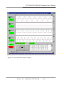
The demo program of post-trigger is given as follows:
wRetVal=P180X_ClearScan();
wRetVal += P180X_AddToScan(0,0,1,0,0,0);
// CH:0 to scan
wRetVal += P180X_SaveScan(0,wV0);
wRetVal += P180X_AddToScan(2,0,1,0,0,0);
// CH:2 to scan
wRetVal += P180X_SaveScan(1,wV2);
// Notice: 1 not 2
//
^ : This is a ordinal number in
// Scan Queue not a channel number.
wRetVal += P180X_StartScanPostTrg(wSampleRateDiv,DATALENGTH,nPriority);
if (wRetVal==0) sprintf(cShow,"2. External Post-Trigger Setup OK");
else sprintf(cShow,"2. External Post-Trigger Setup Error");
TextOut(hdc,x*dx,(y+iLine)*dy,cShow,strlen(cShow)); iLine++;
for (; ;)
{
P180X_ReadScanStatus(&wStatus,&dwLowAlarm,&dwHighAlarm);
if (wStatus>1) break;
Sleep(10);
}
sprintf(cShow,"3. ScanStatus=%x",wStatus);
TextOut(hdc,x*dx,(y+iLine)*dy,cShow,strlen(cShow)); iLine++;
wRetVal=P180X_StopMagicScan();
if (wRetVal!=NoError)
{
sprintf(cShow,"4. StopMagicScan Error");
TextOut(hdc,x*dx,(y+iLine)*dy,cShow,strlen(cShow)); iLine++;
for (dwI=0; dwI<100; dwI++) Beep(10,10);
}
SHOW_WAVE(hwnd,LINE1,wV0,1);
SHOW_WAVE(hwnd,LINE2,wV2,1);
z
Refer to DEMO23.C for completely source program
Version: 3.8
(Mar.2007, PPH-014-38)
---- 50
PCI-1202/1602/1800/1802 Hardware User’s Manual
The B13 must set to 1 to set the external trigger logic. The external trigger controller
commands are given as follows:
Trigger
Command sequences
Descriptions
[B12, B11, B10 ]
Disable external trigger
[ 1, 0, X]
Disable all external trigger.
[ 1, 0, X]
(1) disable all external trigger
(2) set pacer time-1
(3) clear FIFO and disable timer-1
(4) waiting for external signal to enable timer-1
(5) fetch N data
(6) stop all timer & disable all external trigger
(for PCI-1800/1X02)
Post-trigger
(for
PCI-1202/1602/
[ 1, 0, X ]
1800/1802)
[ 1, 1, 1 ]
[ 1, 0, X]
Pre-trigger
[ 1, 0, X ]
(1) disable all external trigger
(2) set pacer timer-1
[ 0, 1, X ]
(3) clear FIFO and enable timer-1
(4) waiting for the external signal to stop timer-1.
(5) circular-fetch the last N data
(6) stop all timer & disable all trigger
(for PCI-1202/1602 &
PCI-1800/1802/ver-F)
[ 1, 1, 0 ]
[ 1, 0, X]
[ 1, 0, X ]
Middle-trigger
(for PCI-1202/1602 &
[ 0, 1, X ]
PCI-1800/1802/ver-F)
[ 1, 1, 1]
[ 1, 0, X]
Pre-trigger
(for
[ 1, 0, X]
(5) keep the last N data (circular-fetch)
(6) stop all timer & disable all trigger
PCI-1800/1802)
[ 0, 1, X ]
Middle-trigger
(for
[ 1, 1, 1]
(1) disable all external trigger
(2) set pacer timer-1
(3) clear FIFO and enable timer-1
(4) waiting for the external signal to stop timer-1.
[ 1, 0, X ]
(version-C)
[ 1, 0, X ]
PCI-1800/1802)
(version-C)
(1) disable all external trigger
(2) set pacer timer-1
(3) clear FIFO and enable timer-1
(4) waiting for the external signal.
(5) fetch more N2 data (circular-fetch)
(6) stop all timer & disable all trigger
[ 0, 1, X ]
[ 1, 1, 0]
[ 0, 1, X]
[ 1, 0, X]
Version: 3.8
(1) disable all external trigger
(2) set pacer timer-1
(3) clear FIFO and enable timer-1
(4) waiting for the external signal to stop timer-1
(5) enable timer-1
(6) fetch more N2 data
(7) stop all timer & disable all trigger
(Mar.2007, PPH-014-38)
---- 51
PCI-1202/1602/1800/1802 Hardware User’s Manual
The Windows driver of post-trigger is given as follows:
WORD CALLBACK P180X_StartScanPostTrg(WORD wSampleRateDiv, DWORD dwNum,
SHORT nPriority)
{
disable_timer0(); // disable internal pacer timer
disable_timer1(); // disable external pacer timer
wVal=pic_control(0xD400); /* 11?1 01?? ???? ???? cmd_101=start scan */
if (wVal!=0) return(wVal);
_outpw(wAddrCtrl,0xf000);
enable_timer1(wSampleRateDiv);
_outpw(wAddrCtrl,0x7000);
_outpw(wAddrCtrl,0xf000);
_outpw(wAddrCtrl,0xfc00);
// 1. disable all external trigger
// 2. Sampling rate=8M/dwSampleRateDiv
// 3. B15=0,S2=1,S1=S0=0 --> clr FIFO
// 3. B15=1,S2=1,S1=S0=0 --> disable timer-1
// 4. S2=1, S1=1, S0=1 --> wait ext signal to
//
enable timer-1
// create magicscan thread
InitializeCriticalSection(&MagicScan_CS);
wThreadStatus=0; wAskThreadStop=0;
hThread=CreateThread(NULL,0,(LPTHREAD_START_ROUTINE)magic_scan,
NULL, 0,&dwThreadID);// can use all MagicScan functions
SetThreadPriority(hThread,nPriority);
i=0;
for(;;)
{
EnterCriticalSection(&MagicScan_CS);
j=wThreadStatus;
LeaveCriticalSection(&MagicScan_CS);
if (j!=0) break;
i++; Sleep(1);
if (i>1000) return(ThreadCreateError);
}
return(NoError);
}
z
z
P1202_StartScanPostTrg(…) is designed for PCI-1202H/L/HU/LU
P1602_StartScanPostTrg(…) is designed for PCI-1602 and PCI-1602F
Version: 3.8
(Mar.2007, PPH-014-38)
---- 52
PCI-1202/1602/1800/1802 Hardware User’s Manual
The windows driver of pre-trigger is given as follows:
WORD CALLBACK P180X_StartScanPreTrg(WORD wSampleRateDiv, DWORD dwNum,
SHORT nPriority)
{
disable_timer0(); // disable internal pacer timer
disable_timer1(); // disable external pacer timer
wVal=pic_control(0xD400); /* 11?1 01?? ???? ???? cmd_101=start scan */
if (wVal!=0) return(wVal);
_outpw(wAddrCtrl,0xf000);
enable_timer1(wSampleRateDiv);
_outpw(wAddrCtrl,0x6800);
_outpw(wAddrCtrl,0xE800);
_outpw(wAddrCtrl,0xF800);
// 1. disable all external trigger
// 2. Sampling rate=8M/dwSampleRateDiv
// 3. B15=0,S2=0,S1=1,S0=0 --> clr FIFO
// 3. B15=1,S2=0,S1=1,S0=0 --> enable timer-1
// 4. S2=1; S1=1; S0=0 --> wait ext signal to
//
disable timer-1
// create magicscan thread
InitializeCriticalSection(&MagicScan_CS);
wThreadStatus=0; wPreMid=0; wAskThreadStop=0; // pre-trigger
hThread=CreateThread(NULL,0,(LPTHREAD_START_ROUTINE)
magic_scan_pre_mid_trg, NULL, 0,&dwThreadID);
SetThreadPriority(hThread,nPriority); // can not use HI/LO alarm & digital filter
i=0;
for(;;)
{
EnterCriticalSection(&MagicScan_CS);
j=wThreadStatus;
LeaveCriticalSection(&MagicScan_CS);
if (j!=0) break;
i++; Sleep(1);
if (i>1000) return(ThreadCreateError);
}
return(NoError);
}
z
z
P1202_StartScanPostTrg(…) is designed for PCI-1202H/L/HU/LU
P1602_StartScanPostTrg(…) is designed for PCI-1602 and PCI-1602F
Version: 3.8
(Mar.2007, PPH-014-38)
---- 53
PCI-1202/1602/1800/1802 Hardware User’s Manual
The windows driver of middle-trigger is given as follows:
WORD CALLBACK P180X_StartScanMiddleTrg(WORD wSampleRateDiv, DWORD
dwNum, SHORT nPriority)
{
disable_timer0(); // disable internal pacer timer
disable_timer1(); // disable external pacer timer
wVal=pic_control(0xD400); /* 11?1 01?? ???? ???? cmd_101=start scan */
if (wVal!=0) return(wVal);
_outpw(wAddrCtrl,0xf000);
enable_timer1(wSampleRateDiv);
_outpw(wAddrCtrl,0x6800);
_outpw(wAddrCtrl,0xE800);
_outpw(wAddrCtrl,0xFC00);
// 1. disable all external trigger
// 2. Sampling rate=8M/dwSampleRateDiv
// 3. B15=0,S2=0,S1=1,S0=0 --> clr FIFO
// 3. B15=1,S2=0,S1=1,S0=0 --> enable timer-1
// 4. S2=1; S1=1; S0=1 --> wait ext signal
// create magicscan thread
InitializeCriticalSection(&MagicScan_CS);
wThreadStatus=0; wPreMid=1; wAskThreadStop=0; // middle-trigger
hThread=CreateThread(NULL,0,(LPTHREAD_START_ROUTINE,
magic_scan_pre_mid_trg, NULL, 0,&dwThreadID);
SetThreadPriority(hThread,nPriority); // can not use HI/LO alarm & digital filter
i=0;
for(;;)
{
EnterCriticalSection(&MagicScan_CS);
j=wThreadStatus;
LeaveCriticalSection(&MagicScan_CS);
if (j!=0) break;
i++; Sleep(1);
if (i>1000) return(ThreadCreateError);
}
return(NoError);
}
z
z
P1202_StartScanPostTrg(…) is designed for PCI-1202H/L/HU/LU
P1602_StartScanPostTrg(…) is designed for PCI-1602 and PCI-1602F
Version: 3.8
(Mar.2007, PPH-014-38)
---- 54
PCI-1202/1602/1800/1802 Hardware User’s Manual
The pre-trigger driver for PCI-1800/1802/ver-C is given as follows:
WORD CALLBACK P180X_StartScanPreTrgVerC(WORD wSampleRateDiv, DWORD
dwNum, SHORT nPriority)
{
disable_timer0(); // disable internal pacer timer
disable_timer1(); // disable external pacer timer
wVal=pic_control(0xD400); /* 11?1 01?? ???? ???? cmd_101=start scan */
if (wVal!=0) return(wVal);
_outpw(wAddrCtrl,0xf000);
enable_timer1(wSampleRateDiv);
_outpw(wAddrCtrl,0x6800);
_outpw(wAddrCtrl,0xE800);
_outpw(wAddrCtrl,0xF800);
// 1. disable all external trigger
// 2. Sampling rate=8M/dwSampleRateDiv
// 3. B15=0,S2=0,S1=1,S0=0 --> clr FIFO
// 3. B15=1,S2=0,S1=1,S0=0 --> enable timer-1
// 4. S2=1; S1=1; S0=0 --> wait ext signal to
//
disable timer-1
// create magicscan thread
InitializeCriticalSection(&MagicScan_CS);
wThreadStatus=0; wPreMid=0; wAskThreadStop=0; // pre-trigger
hThread=CreateThread(NULL,0,(LPTHREAD_START_ROUTINE,
magic_scan_pre_mid_trg_ver_c, NULL, 0,&dwThreadID);
SetThreadPriority(hThread,nPriority);
i=0;
for(;;)
{
EnterCriticalSection(&MagicScan_CS);
j=wThreadStatus;
LeaveCriticalSection(&MagicScan_CS);
if (j!=0) break;
i++; Sleep(1);
if (i>1000) return(ThreadCreateError);
}
return(NoError);
}
z
This driver is designed for PCI-1800/1802 version-C
Version: 3.8
(Mar.2007, PPH-014-38)
---- 55
PCI-1202/1602/1800/1802 Hardware User’s Manual
The middle-trigger driver for PCI-1800/1802/ver-C is given as follows:
WORD CALLBACK P180X_StartScanMiddleTrgVerC(WORD wSampleRateDiv, DWORD
dwNum, SHORT nPriority)
{
disable_timer0(); // disable internal pacer timer
disable_timer1(); // disable external pacer timer
wVal=pic_control(0xD400); /* 11?1 01?? ???? ???? cmd_101=start scan */
if (wVal!=0) return(wVal);
_outpw(wAddrCtrl,0xf000);
enable_timer1(wSampleRateDiv);
_outpw(wAddrCtrl,0x6800);
_outpw(wAddrCtrl,0xE800);
_outpw(wAddrCtrl,0xF800);
// 1. disable all external trigger
// 2. Sampling rate=8M/dwSampleRateDiv
// 3. B15=0,S2=0,S1=1,S0=0 --> clr FIFO
// 3. B15=1,S2=0,S1=1,S0=0 --> enable timer-1
// 4. S2=1; S1=1; S0=0 --> wait ext signal to
//
disable timer-1
// create magicscan thread
InitializeCriticalSection(&MagicScan_CS);
wThreadStatus=0; wPreMid=1; wAskThreadStop=0; // middle-trigger
hThread=CreateThread(NULL,0,(LPTHREAD_START_ROUTINE,
magic_scan_pre_mid_trg_ver_c, NULL, 0,&dwThreadID);
SetThreadPriority(hThread,nPriority);
i=0;
for(;;)
{
EnterCriticalSection(&MagicScan_CS);
j=wThreadStatus;
LeaveCriticalSection(&MagicScan_CS);
if (j!=0) break;
i++; Sleep(1);
if (i>1000) return(ThreadCreateError);
}
return(NoError);
}
z
This driver is designed for PCI-1800/1802 version-C
Version: 3.8
(Mar.2007, PPH-014-38)
---- 56
PCI-1202/1602/1800/1802 Hardware User’s Manual
The external trigger drivers are given as follows:
Driver Name
demo
program
Applications
P180X_StartScanPostTrg(…)
demo23.c
for PCI-1800/1802 ver-C & verF
P180X_StartScanPreTrg(…)
demo24.c
for PCI-1800/1802 ver-F
P180X_StartScanMiddleTrg(…)
demo25.c
for PCI-1800/1802 ver-F
P180X_StartScanPreTrgOld(…)
demo26.c
for PCI-1800/1802 ver-C
P180X_StartScanMiddleTrgOld(…) demo27.c
for PCI-1800/1802 ver-C
P1202_StartScanPostTrg(…)
demo23.c
for PCI-1202
P1202_StartScanPreTrg(…)
demo24.c
for PCI-1202
P1202_StartScanMiddleTrg(…)
demo25.c
for PCI-1202
P1602_StartScanPostTrg(…)
demo23.c
for PCI-1602
P1602_StartScanPreTrg(…)
demo24.c
for PCI-1602
P1602_StartScanMiddleTrg(…)
demo25.c
for PCI-1602
3.6.1.9 Clear FIFO Bit
The B15 is used to reset the on-board FIFO. When set to low, FIFO will be clear. The
FIFO must be clear once after power-on.
The demo program of handshaking is given as follows:
// Clear FIFO to clear all data
outport(wAddrCtrl,0x2000); /* Bit15=0=clear FIFO, Bit13=1=not PIC cmd */
outport(wAddrCtrl,0xA000); /* Bit15=1=no reset FIFO, BIT13=1=not PIC cmd */
Version: 3.8
(Mar.2007, PPH-014-38)
---- 57
PCI-1202/1602/1800/1802 Hardware User’s Manual
3.6.1.10 Handshake Control Bit
Set the B13 to 0 if the command is sent to the MagicScan controller. Keep this bit at high
when not used.
The demo program of handshaking is given as follows:
WORD pic_control(WORD i)
{
WORD j;
if ((inport(wAddrCtrl)&0x04)==0)
{
outport(wAddrCtrl,0xffff);
/* send a recovery to PIC */
}
j=0;
while ((inport(wAddrCtrl)&0x04)==0)
{
j++;
if (j>65530) return(AdControllerError); /* time out */
}
i = i & 0xDFFF;
/* set pic low !! */
outport(wAddrCtrl,i);
j=0;
while ((inport(wAddrCtrl)&0x04)!=0)
{
j++;
if (j>65530) return(AdControllerError); /* time out */
}
outport(wAddrCtrl,(WORD)(i | 0x2000)); /* set pic high !! */
j=0;
while ((inport(wAddrCtrl)&0x04)==0)
{
j++;
if (j>65530) return(AdControllerError); //time out
}
return(NoError);
}
Version: 3.8
(Mar.2007, PPH-014-38)
---- 58
PCI-1202/1602/1800/1802 Hardware User’s Manual
3.6.2 The status register
The format of the status register is given as follows:
Bit7 Bit6 Bit5 Bit4 Bit3 Bit2 Bit1 Bit0
LSB
MSB
0 Æ FIFO is half-full.
0 Æ FIFO is full.
0 Æ FIFO is empty.
0 Æ ADC is busy.
For PCI-180x Ver. C: 0 Æ timer-1 is disable
1 Æ timer-1 is enable
For PCI-180x Ver. F: 0 Æ waiting external trigger signal
1 Æexternal trigger signal is active.
Bit 2: handshake signal between host (PC) and MagicScan controller.
Bit 1: ODM indicator: non-ODM version Æ 0.
ODM version Æ ODM bit string.
Bit 0: Output of machine independent timer. This bit is equal to 0 if the machine
independent timer is start. This bit will be set to 1 if the machine independent timer
is up.
Bit 7: FIFO half-full
Bit 6: FIFO full
Bit 5: FIFO empty
Bit 4: ADC busy
Bit 3: External trigger
:
:
:
:
:
Version: 3.8
(Mar.2007, PPH-014-38)
---- 59
PCI-1202/1602/1800/1802 Hardware User’s Manual
3.6.3 The A/D software trigger register
Writing to this port will perform a software to trigger an A/D conversion. Although the
PC can send very fast trigger signal (more than 333K ), the max. sampling rate of A/D
conversion can not over 330K samples/second. The timing diagram is given as follows:
Delay time
Software
trigger
A/D
Busy
3μs
Conversion Time
Figure 3-3: Trigger delay time.
The demo program of software trigger A/D conversion is given as follows:
WORD P180X_AdPollingHex(Word *AdVal)
{
WORD wVal, wTime;
//Clear FIFO
outport(wAddrCtrl,0x2000); //B15=0=clear FIFO, B13=1=not MagicScan controller cmd
outport(wAddrCtrl,0xA000); //B15=1=no clear FIFO, B13=1= not MagicScan controller cmd
outport((WORD)(wAddrCtrl+4),0xffff); /* generate a software trigger pulse */
wTime=0;
for (;;)
{
wVal=inport(wAddrCtrl)&0x20; // wait for ready signal
if (wVal!=0) break;
/* If B4==1 Æ A/D data ready */
wTime++;
if (wTime>32760) return(AdPollingTimeOut);
}
AdVal=inport(wAddrAdda)&0x0fff; /* Read the available A/D data from FIFO */
return(NoError);
/* 0xffff for PCI-1602/1602F */
}
z
z
P1202_AdPollingHex(…) is designed for PCI-1202H/L/HU/LU
P1602_AdPollingHex(…) is designed for PCI-1602 and PCI-1602F
Version: 3.8
(Mar.2007, PPH-014-38)
---- 60
PCI-1202/1602/1800/1802 Hardware User’s Manual
3.7 Section 4: D/I/O Register
z I/O address of D/I = wAddrDio
z I/O address of D/O = wAddrDio
The PCI-1800/1802 provides 16-channel digital input and 16-channel digital output. All
levels are TTL compatible. The connections diagram and block diagram are given below:
CON2
I/O read
signal.
DI port
Local Data Bus
D0,D1 ... D15
DO port
I/O write
signal
CoN1
Figure 3-4: DIO block diagram.
The D/I port can be connected to the DB-16P. The DB-16P is a 16-channel isolated digital
input daughter board. The D/O port can be connected to the DB-16R or DB-24PR. The DB16R is a 16-channel relay output board. The DB-24R is a 24-channel power relay output board.
The demo program of D/I/O is given as follows:
WORD P180X_Di(WORD *wDi)
{
*wDi=inport(wAddrDio)&0xffff;
return(NoError);
}
WORD P180X_Do(WORD wDo)
{
outport(wAddrDio,wDo);
return(NoError);
}
Version: 3.8
z
z
P1202_Di(…) for PCI-1202
P1602_Di(…) for PCI-1602
z
z
P1202_Do(…) for PCI-1202
P1602_Do(…) for PCI-1602
(Mar.2007, PPH-014-38)
---- 61
PCI-1202/1602/1800/1802 Hardware User’s Manual
3.8 Section 5: A/D & D/A Register
z I/O address of DA-0 = wAddrAdda
z I/O address of DA-1 = wAddrAdda + 1*4
z I/O address of FIFO = wAddrAdda
Writing data to this section will write data to the DACs and reading data from this
port will read the data from A/D FIFO. The read/write operation is given as follows:
Port
Read
Write
Section + 0
A/D FIFO.
DAC1 write.
Section + 4
Reserved
DAC2 write.
The PCI-1800/1802 provides 2 independent 12-bits D/A converters with double buffer,
bipolar voltage output. The output voltage can be ±5V or ±10V selected by J1. When the PCI1800/1802 is first power-on, the D/A will be in the floating state. The D/A will go to the
programmed state after executing D/A output command. The block diagram is given as below:
5 or 10 Vref
Section5 + 0
Select
DA1
Local Data Bus
Analog Output 1
Double Buffer
D0,D1…D11
DA2
Section5 + 4
Analog Output2
Select
Figure 4-2 : D/A output diagram.
Note: The D/A output is floating after first power-on. The D/A output will be enabled after
executing D/A output command. This is the common feature of PCI-1202/1602/1800/1802.
Version: 3.8
(Mar.2007, PPH-014-38)
---- 62
PCI-1202/1602/1800/1802 Hardware User’s Manual
The demo program for D/A is given as follows:
WORD P180X_Da(WORD wDaChannel, WORD wDaVal)
{
z P1202_Da(…) for PCI-1202
if (wDaChannel==0)
/* channel 0 */
z P1602_Da(…) for PCI-1602
{
outport(wAddrAdda,wDaVal);
return(NoError);
}
else if (wDaChannel==1) /* channel_1 */
{
outport((wAddrAdda+4),wDaVal);
return(NoError);
}
else return(DaChannelError);
}
The demo program of software trigger A/D conversion is given as follows:
WORD P180X_AdPollingHex(Word *AdVal)
{
z P1202_AdPollingHex(…) for PCI-1202
WORD wVal, wTime ;
z P1602_AdPollingHex(…) for PCI-1602
//Clear FIFO
outport(wAddrCtrl,0x2000); // B15=0=clear FIFO, B13=1=not MagicScan controller cmd
outport(wAddrCtrl,0xA000); // B15=1=no clear FIFO, B13=1= not MagicScan controller cmd
outport((WORD)(wAddrCtrl+4),0xffff); /* generate a software trigger pulse */
wTime=0;
for (;;)
{
wVal=inport(wAddrCtrl)&0x20; // wait for ready signal
if (wVal!=0) break;
/* if B4==1 Æ A/D data ready */
wTime++;
if (wTime>32760) return(AdPollingTimeOut);
}
AdVal=inport(wAddrAdda)&0x0fff; /* Read the available A/D data from FIFO */
return(NoError);
/* 0x0fff for 12-bit ADC, 0xffff for 16-bit ADC */
}
Version: 3.8
(Mar.2007, PPH-014-38)
---- 63
PCI-1202/1602/1800/1802 Hardware User’s Manual
4. A/D Conversion Operation
4.1 The Configuration Code Table
PCI-1202L/1202LU/1800L/1802L Configuration Code Table
Bipolar/Unipolar Input Signal Range
Gain
Settling Time
Configuration Code
Bipolar
+/- 5V
1
3 us
0x00
Bipolar
+/- 2.5V
2
3 us
0x01
Bipolar
+/- 1.25V
4
3 us
0x02
Bipolar
+/- 0.625V
8
3 us
0x03
Bipolar
+/- 10V
0.5
3 us
0x04
Bipolar
+/- 5V
1
3 us
0x05
Bipolar
+/- 2.5V
2
3 us
0x06
Bipolar
+/- 1.25V
4
3 us
0x07
Unipolar
0V ~ 10V
1
3 us
0x08
Unipolar
0V ~ 5V
2
3 us
0x09
Unipolar
0V ~ 2.5V
4
3 us
0x0A
Unipolar
0V ~ 1.25V
8
3 us
0x0B
PCI-1602 Configuration Code Table
Bipolar/Uniploar
Input Signal Range Gain
Settling Time Configuration Code
Bipolar
+/-10V
1
10 us
0
Bipolar
+/-5V
2
10 us
1
Bipolar
+/-2.5V
4
10 us
2
Bipolar
+/-1.25V
8
10 us
3
PCI-1602F Configuration Code Table
Bipolar/Uniploar
Input Signal Range Gain
Settling Time Configuration Code
Bipolar
+/-10V
1
5 us
0
Bipolar
+/-5V
2
5 us
1
Bipolar
+/-2.5V
4
5 us
2
Bipolar
+/-1.25V
8
5 us
3
Version: 3.8
(Mar.2007, PPH-014-38)
---- 64
PCI-1202/1602/1800/1802 Hardware User’s Manual
PCI-1202H/1202HU/1800H/1802H Configuration Code Table
Bipolar/Unipolar Input Signal Range
Gain
Settling Time
Configuration Code
Bipolar
+/- 5V
1
23 us
0x10
Bipolar
+/- 0.5V
10
28 us
0x11
Bipolar
+/- 0.05V
100
140 us
0x12
Bipolar
+/- 0.005V
1000
1300 us
0x13
Bipolar
+/- 10V
0.5
23 us
0x14
Bipolar
+/- 1V
5
28 us
0x15
Bipolar
+/- 0.1V
50
140 us
0x16
Bipolar
+/- 0.01V
500
1300 us
0x17
Unipolar
0V ~ 10V
1
23 us
0x18
Unipolar
0V ~ 1V
10
28 us
0x19
Unipolar
0V ~ 0.1V
100
140 us
0x1A
Unipolar
0V ~ 0.01V
1000
1300 us
0x1B
4.2 The Unipolar/Bipolar
If the analog input signal is unipolar, you can measure this signal with bipolar setting
(this will reduce resolution). If the analog input is bipolar, you must select bipolar
configuration code to measure this signal.
4.3 The Input Signal Range
If the input range of analog signal is +/- 1V, you can measure this signal wih +/-10V, +/5V, +/-2.5V and +/- 1.25V configuration code setting. The only difference is the resolution.
The resolution of +/- 2.5V is 4 times higher than in +/- 10V setting. Select the correct
configuration code will get the best resolution.
Version: 3.8
(Mar.2007, PPH-014-38)
---- 65
PCI-1202/1602/1800/1802 Hardware User’s Manual
4.4 The Settling Time
If the channel number or gain factor is changed, the hardware need extra time for
signal ready. This is called the settling time. This limitation will apply both to the Fixedchannel mode and MagicScan mode AD conversions. So the user must take care to avoid the
settling error. In the MagicScan mode, the MagicScan controller will control all details. The
MagicScan controller will change the channel number and gain control just after every pacer
trigger signal. Therefore the limitation is “settling time <= pacer timer" in MagicScan
mode.
4.5 How to Delay the Settling Time
In the software trigger mode, the software operation is given as follows:
1. send software trigger pulse
2. delay the settling time
3. read the A/D data
The P180X_DelayUs(...) is a machine independent timer function. Therefore this
function is suitable to delay the settling time. In the pacer trigger mode, the software does
not have to call P180X_DelayUs(...) The only limitation is that the pacer timer must be
longer than the settling time. Refer to Sec. 4.1 for settling time details.
Version: 3.8
(Mar.2007, PPH-014-38)
---- 66
PCI-1202/1602/1800/1802 Hardware User’s Manual
4.6 The AD Conversion Mode
The AD conversion operation of PCI-1202/1602/1800/1802 can be divided into
two different mode: Fixed-channel mode and the MagicScan mode.
•
1.
2.
3.
4.
•
1.
2.
3.
4.
5.
6.
The functions of fixed-channel mode are given as follows:
P180X_SetChannelConfig
The reading data is in
P180X_AdPolling
double format
P180X_AdsPolling
P180X_AdsPacer
The functions of MagicScan mode are given as follows:
P180X_ClearScan
Data in 12 bits HEX format
P180X_StartScan
P180X_ReadScanStatus
P180X_AddToScan
P180X_SaveScan
P180X_WaitMagicScanFinish
7. P180X_StartScanPostTrg
8. P180X_StartScanPreTrg
9. P180X_StartScanMiddleTrg
7.
8.
9.
For external trigger
For external trigger
For external trigger
•
The functions of M_functions are given as follows:
1.
2.
3.
4.
P180X_M_FUN_1
P180X_M_FUN_2
P180X_M_FUN_3
P180X_M_FUN_4
Version: 3.8
(Mar.2007, PPH-014-38)
---- 67
PCI-1202/1602/1800/1802 Hardware User’s Manual
•
1.
2.
3.
4.
•
The functions of continuous capture with storing data to main memory are given as
follows: (two board operating simultaneously)
P180X_FunA_Start
P180X_FunA_ReadStatus
P180X_FunA_Stop
P180X_FunA_Get
The functions of continuous capture with storing data to main memory are given as
follows: (single board operating)
1.
2.
3.
4.
P180X_FunB_Start
P180X_FunB_ReadStatus
P180X_FunB_Stop
P180X_FunB_Get
•
The functions of continuous capture are given as follows:
1.
2.
3.
4.
5.
6.
P180X_Card0_StartScan
P180X_Card0_ReadStatus
P180X_Card0_StopScan
P180X_Card1_StartScan
P180X_Card1_ReadStatus
P180X_Card1_StopScan
Version: 3.8
Group-0: for card_0 continuous capture function
Group-1: for card_1 continuous capture function
(Mar.2007, PPH-014-38)
---- 68
PCI-1202/1602/1800/1802 Hardware User’s Manual
4.7 The Fixed-channel Mode AD Conversion
The P180X_SetChannelConfig will active the selected channel and its configuration
code. Then the other functions will refer to that channel and configuration. The general flow
chart is given as follows :
P180X_SetChannelConfig
P180X_DelayUs
P180X_AdPolling
Delay the settling time (if needed)
Perform one AD conversion
AD data Analysis
Analyses of the AD dada 1
P180X_SetChannelConfig
Select the active channel 2
P180X_DelayUs
Delay the settling time (if needed)
P180X_AdPolling
Perform one AD conversion
AD data Analysis
Analyses of the AD dada 2
P180X_SetChannelConfig
Select the active channel ?
P180X_DelayUs
z
z
Select the active channel 1
Delay the settling time (if needed)
P180X_AdPolling
Perform one AD conversion
AD data Analysis
Analyses of the AD dada ?
P1202_SetChannelConfig(…) is designed for PCI-1202H/L/HU/LU
P1602_SetChannelConfig(…) is designed for PCI-1602 and PCI-1602F
Version: 3.8
(Mar.2007, PPH-014-38)
---- 69
PCI-1202/1602/1800/1802 Hardware User’s Manual
4.8 The MagicScan Mode AD Conversion
The P180X_ClearScan will set the MagicScan controller to its initial state. The
P180X_AddToScan will add the channels to MagicScan circular queue one by one. The order
of P180X_AddToScan is the scan order. The maximum queue size is 48. The scan order is
random and can be repeat. The AD data will not save in the normal condition. The AD data of
MagicScan can be saved in array if P180X_SaveScan is used. The flowchart is given as
follows:
P180X_ClearScan
Clear the MagicScan controller
P180X_AddToScan
Add channel 1 to circular
P180X_SaveScan
If the AD data need to save
P180X_AddToScan
Add channel 2 to circular
P180X_SaveScan
If the AD data need to save
P180X_AddToScan
Add channel ? to circular
P180X_SaveScan
P180_StartScan
P180X_WaitMagicScanFinish
If the AD data need to save
Start the MagicScan operation
Wait until MagicScan finished
Perform Aanlysis
z
z
P1202_ClearScan(…) is designed for PCI-1202H/L/HU/LU
P1602_ClearScan(…) is designed for PCI-1602 and PCI-1602F
Version: 3.8
(Mar.2007, PPH-014-38)
---- 70
PCI-1202/1602/1800/1802 Hardware User’s Manual
4.8.1 The MagicScan Circular_Scan_Queue
The MagicScan controller equips a circular queue for scan sequence control. The scan
sequence is one by one and repeatable with the limitation of maximum 48 channels. So the
following scan sequence are all validate :
One channel MagicScan
0
Two channels MagicScan, scan
0
1
1
0
0
0
1
2
3
Three channels MagicScan : 123123123
2
5
1
Three channels MagicScan : 251251251
2
5
2
Three channels MagicScan : 252252252
1
2
Two channels MagicScan, scan
Two channels MagicScan, scan
1
3
Version: 3.8
Four channels MagicScan : 12131213
(Mar.2007, PPH-014-38)
---- 71
PCI-1202/1602/1800/1802 Hardware User’s Manual
4.8.2 The Digital Filter of MagicScan
The digital filter is a average filter.
Filter value = (V_1+V_2+……+V_n)/n, where n is average factor
If the input signal is very noisy, this filter can be used to remove these noises.
4.8.3 The Different Sampling Rate of MagicScan
The MagicScan controller scans the analog inputs in fixed-sampling-rate. The
different sampling rate is implemented with averaging technique. This technique is the
same as the digital filter described in Sec. 4.8.2. If the user wishes to use the different
sampling rate, the digital filter will be active at the same time. This is a situation of ALL
or NO. You can use both the digital filter and the different sampling rate at the same
time or use neither of them.
P180X_ClearScan();
P180X_AddToScan(?,?,10,….); Æ only one channel scan
P180X_StartScan(?,24); Æ the AD sampling rate = 8M/24=333K
Æ the factor=10 Æ sampling rate=333K/10=33.3K
P180X_ClearScan();
P180X_AddToScan(A,?,1,….);
P180X_AddToScan(B,?,2,….);
P180X_AddToScan(C,?,3,….);
P180X_StartScan(?,24); Æ the AD sampling rate = 8M/24=333K
Æ scan sampling rate=333K/3=111K
channel_A sampling rate=111K/1=111K
channel_B sampling rate=111K/2=55.5K
channel_C sampling rate=111K/3=37K
z
z
P1202_ClearScan(…) is designed for PCI-1202H/L/HU/LU
P1602_ClearScan(…) is designed for PCI-1602 and PCI-1602F
Version: 3.8
(Mar.2007, PPH-014-38)
---- 72
PCI-1202/1602/1800/1802 Hardware User’s Manual
4.8.4 The High/Low Alarm of MagicScan
There are 5 alarm types are given as follows:
Type 0 : no alarm
Type 1 : high alarm
Type 2 : low alarm
Type 3 : in alarm
Type 4 : out alarm
Æ any AD data > High_alarm_value
Æ any AD data < Low_alarm_value
Æ Low_alarm_value < any AD data < High_alarm_value
Æ any AD data < Low_alarm_value or
any AD data > High_alarm_value
All the alarm_value are defined in HEX format
Version: 3.8
(Mar.2007, PPH-014-38)
---- 73
PCI-1202/1602/1800/1802 Hardware User’s Manual
4.8.5 The MagicScan Function
The features of MagicScan are given as follows:
1. Different gain for each channel
2. Non-sequential order for channel scan
3. Different sampling rate for each channel (use with digital filter)
4. Programmable different digital filter for each scan channel
5. Programmable HI/LO alarm for each channel
6. Three external trigger: post-trigger, pre-trigger and middle-trigger
7. Maintain at 330K max. for total channel scan
8. Easy programming
The MagicScan function is implemented with software and hardware. The feature 1 and
feature 2 are implemented in hardware. The other features are implemented in software. The
block diagram of MagicScan function is given as follows:
Magic Scan
Controller
Analog
Signal
:
:
MUX
PGA
A/D
Converter
FIFO
X86
Pacer Trigger
Timer
(1) The Magic Scan controller is a high performance RISC-like controller. It can scan the
analog input signal in non-sequential order. It also control the PGA to different
predefined gain for each channel.
(2) The pacer trigger timer will be generated the trigger signal to A/D converter.
(3) The A/D conversion data will enter the FIFO.
(4) The X86 will read and analyze the A/D data from FIFO while the CPU is ready. The
FIFO is 2K for PCI-1800 and 8K for PCI-1802. The X86 will compute and analyze the A/D
data while the A/D conversion is going. Therefore the speed of X86 must compatible with the
speed of A/D conversion. The A/D conversion can be 330K max. in the channel/scan mode.
Therefore the X86 must handle 330K samples per second to avoid overflow. The Pentium-120
CPU or more powerful CPU is recommended.
Version: 3.8
(Mar.2007, PPH-014-38)
---- 74
PCI-1202/1602/1800/1802 Hardware User’s Manual
The A/D conversion data in FIFO are in the same sampling rate (refer to (1), (2), (3)).
For example,
z the scan channel is 1Æ 2 Æ 3
z the pacer sampling rate is 330K
z the expected sampling rate for channel 1 is 110K
z the expected sampling rate for channel 2 is 55K
z the expected sampling rate for channel 3 is 11K
The hardware will scan the analog data into FIFO as follows:
1,2,3,1,2,3,1,2,3,1,2,3,1,2,3,1,2,3……
Æ total 330K
Æ every 1,1,1,1,1 is 110K
Æ every 2,2,2,2,2 is 110K
Æ every 3,3,3,3,3 is 110K
The software has to fetch the 2,2,2,2,2 in 55K, therefore the software average the
continue two 2 into one 2 to get 55K as follows:
2,2, 2,2 2,2, 2,2
2,
2, 2,
2, Æ 55K
The software has to fetch the 3,3,3,3,3 in 11K, therefore the software average the
continue ten 3 into one 3 to get 11K.
There are very heavy computation load for the X86 to execute the MagicScan function.
These computation loads are given as follows:
1. average the continue N data into one data to get different sampling rate data
2. compare each A/D data with the HI/LO alarm limit
3. save the A/D data into memory if the save flag is enable
The MagicScan function described in this section can be realized in Pentium-120 &
Windows 95.
Refer to Sec. 4.8.6 for driver source.
Refer to Chapter 8 for demo program.
Refer to Chapter 10 for performance evaluation.
Version: 3.8
(Mar.2007, PPH-014-38)
---- 75
PCI-1202/1602/1800/1802 Hardware User’s Manual
4.8.6 The MagicScan Thread
//---------------------------------------------------------------------// wThreadStatus : 0x01=MagicScan start
//
0x02=timeout1
//
0x04=timeout2
//
0x08=FIFO overflow
//
0x80=MagicScan OK
WORD magic_scan()
{
WORD wVal,w1,w3;
DWORD i,dwTime,j,k,dwIndex;
for (j=0; j<wMP; j++) dwMagicSum[j]=0;
for (j=0; j<wMP; j++) wMagicNow[j]=wMagicAve[j];
for (j=0; j<wMP; j++) wMagicP[j]=0;
for (i=0; i<wMP; i++) // skip the MagicScan settling time
{
dwTime=0;
for (;;)
{
wVal=inport(wAddrCtrl)&0x20;
if(wVal!=0) break;
dwTime++;
if(dwTime>100000)
return TimeOut;
}
inport(wAddrAdda)&0xffff;
}
dwMagicLowAlarm=0;
dwMagicHighAlarm=0;
for(i=0; i<wMagicNum; i++)
{
for (j=0; j<wMP; j++)
{
dwTime=0;
Version: 3.8
(Mar.2007, PPH-014-38)
---- 76
PCI-1202/1602/1800/1802 Hardware User’s Manual
for (;;)
{
wVal=inport(wAddrCtrl)&0x60;
if (wVal==0x20) return FifoOverflow;
if (wVal==0x60) break;
dwTime++;
if (dwTime>100000) return TimeOut;
}
dwMagicSum[j]+=(inport(wAddrAdda)&0x0fff); /* 0x0fff for 12-bitADC, 0xffff for 16-bit ADC */
wMagicNow[j]--;
w1=wMagicNow[j];
if (w1==0)
{
wVal=(WORD)(dwMagicSum[j]/wMagicAve[j]);
if (wMagicScanSave[j]==1)
{
*((wMagicScanBuf[j])+wMagicP[j])=wVal;
wMagicP[j]++;
}
w3=wMagicAlarmType[j];
if(w3>0)
// 0 = no alarm
{
dwIndex=0x01; k=j;
while (k>0)
{
dwIndex=dwIndex<<1;
k--;
}
if (w3==2) // 2 = low alarm
{
if (wVal<wMagicLowAlarm[j]) dwMagicLowAlarm |= dwIndex;
}
else if (w3==1) // 1 = high alarm
{
if (wVal>wMagicHighAlarm[j]) dwMagicHighAlarm |= dwIndex;
}
else if (w3==4) // 4 = high or low alarm
{
Version: 3.8
(Mar.2007, PPH-014-38)
---- 77
PCI-1202/1602/1800/1802 Hardware User’s Manual
if (wVal<wMagicLowAlarm[j]) dwMagicLowAlarm |= dwIndex;
if (wVal>wMagicHighAlarm[j]) dwMagicHighAlarm |= dwIndex;
}
else if (w3==3) // 3 = in [low,high] alarm
{
if ((wVal>wMagicLowAlarm[j])&& (wVal<wMagicHighAlarm[j]))
{
dwMagicLowAlarm |= dwIndex;
dwMagicHighAlarm |= dwIndex;
}
}
}
dwMagicSum[j]=0;
wMagicNow[j]=wMagicAve[j];
} // end if(w1
} // end for(j=
} // end for(i=
ret_label:
disable_timer0();
return 0;
}
Version: 3.8
(Mar.2007, PPH-014-38)
---- 78
PCI-1202/1602/1800/1802 Hardware User’s Manual
5. M_Function
Some real world applications have to send out the pre-defined pattern to the external
device and measure the output responses for analysis. The user need one arbitrary wave form
generator and one high speed A/D converter. The M_Functions, provided by PCI1202/1602/1800/1802, can send out the user defined arbitrary waveform and perform the
A/D conversion at the same time.
The M_Functions can be executed under DOS, Windows 95/98 and Windows
NT/2000. Some programming languages(VC++, BC++, VB, Delphi, BCB) and
package(LabVIEW and more) can call the M_Functions now. The spectrum output response
of the M_FUN_1 by LabView 4.0 is given as follows.
Figure 5-1: The spectrum output response of M_FUN_1.
Version: 3.8
(Mar.2007, PPH-014-38)
---- 79
PCI-1202/1602/1800/1802 Hardware User’s Manual
5.1 Introduction
z
What Is M_Functions?
The features of the M_Functions are given as follows:
1. Arbitrary wave form generation from D/A output port (2 channels max.)
2. Perform MagicScan A/D conversion at the same time (32 channels max.)
3. Only one function call is needed
4. Very easy to use
The user can send out the D/A wave form output to the external device and measure the
response(32 channels max.) at the same time. The block diagram of the M_Functions is given
as follows:
M Functions
DA1
DA2
External Device
Input 1
Input 2
Response 1
Response N
ADn
AD1
Figure 5-2: The block diagram of M-Functions.
z
Which types of waveform can be generated by the M_Functions ?
The M_Functions use wave-form-image-data format to reconstruct the output waveform.
Therefore nearly any types of waveform can be generated. The only limitations are resolution
and frequency. It is very difficult to generate a very high resolution and high frequency
waveform.
If the user want to generate the periodic wave form such as sine, cosine,...., the
M_Functions can provide the output wave form over 100K samples/sec. The +/- 5V 100Ks/s
sine wave shown in Figure 5-3 and +/- 5V 200Ks/s sine wave shown in Figure 5-4 are all
generated by M_Function1. The Figure 5-3 and Figure 5-4 is measured by Tektronix TDS 220.
The display resolution of TDS 220 is limited, so the output waveform does not look smooth.
The real output waveform is smooth.
Version: 3.8
(Mar.2007, PPH-014-38)
---- 80
PCI-1202/1602/1800/1802 Hardware User’s Manual
Figure 5-3: The M_Function_1 send out a 100K, +/- 5V sine wave.
(measured by Tektronix TDS 220)
Figure 5-4: The M_Function_1 send out a 200K, +/-5V sine wave.
(measured by Tektronix TDS 220)
Version: 3.8
(Mar.2007, PPH-014-38)
---- 81
PCI-1202/1602/1800/1802 Hardware User’s Manual
z How many M_Functions are ready now ?
There are four M_Functions, P180X_M_FUN_1, P180X_M_FUN_2, P180X_M_FUN_3
and M_FUN_4 are ready now. The M_FUN_1 will automatic to compute the sine wave output
image. The M_FUN_2 is designed for arbitrary waveform generation, so the user can prepare
their waveform for M_FUN_2. The M_FUN_3 is similar to M_FUN_1 except the A/D input
channels are programmable. The comparison table is given as follows:
driver name
D/A
A/D
P180X_M_FUN_1
Channel_0, sine wave
channel_0, ±10V
P180X_M_FUN_2
Channel_0, arbitrary wave form
channel_0, ±10V
P180X_M_FUN_3
Channel_0, sine wave
channel/gain programmable
(32 channels max.)
P180X_M_FUN_4
Channel_0, square wave or semi- channel/gain programmable
square-wave or sine wave
(32 channels max.)
Because the M_Functions are so powerful, we accept special design request (OEM or
ODM). The user can e-mail the request to [email protected]
z Which cards support the M_Functions ?
The PCI-1800H/L, PCI-1802H/L, PCI-1602, PCI-1602F and PCI-1202H/L/HU/LU can
support M_Functions now.
z Which operating systems support the M_Functions ?
The M_Functions can be executed under DOS, Windows 95/98, Windows NT 4.0/2000/XP
now.
Version: 3.8
(Mar.2007, PPH-014-38)
---- 82
PCI-1202/1602/1800/1802 Hardware User’s Manual
z Limitation
The system will interrupt the driver software under Windows 95/NT. The partial function
of D/A arbitrary waveform generation is implemented by software. Therefore the D/A output
waveform will be distorted sometimes. Refer to Figure 5-5 for details.
If the user has to generate the periodic wave form such as sin, cos …, and the analysis is
similar to spectrum analysis, this type of output distortion will cause little trouble. The D/A
output maybe distorted but spectrum response is still stable.
If the user uses DOS, the D/A output waveform will not be distorted in any time.
Figure 5-5: The D/A waveform is distorted but the spectrum response is nearly the same.
Version: 3.8
(Mar.2007, PPH-014-38)
---- 83
PCI-1202/1602/1800/1802 Hardware User’s Manual
6. Continuous Capture Functions
The continuous capture functions are very useful in real world applications. It can be
used many types of applications. Those applications are
1. Low speed, no storage, real-time processing, continuous capture
2. High speed, store the A/D data in PC main memory, time is limited by memory size
(Referring to P180X_FunA series functions and P180X_FunB series function for more
Detail information in 6.2)
3. High speed, store the A/D data in the external NVRAM, time is limited by memory size
6.1 General Purpose Driver
The PCI-1202/1602/1800/1802 is very suitable for these three applications. The software driver
can support 16 cards max. in one PC system. The software of version 2.0 only support 2 cards
for continuous capture function. The software 3.0 will support more cards. The continuous
capture functions are special designed into many groups. Each group is corresponding to one
card. There are three functions included in a group as follows:
1.
2.
3.
P180X_Card0_StartScan(…)
P180X_Card0_ReadStatus(…)
P180X_Card0_StopScan(….)
Group-0: for card_0 continuous capture function
1.
2.
3.
P180X_Card1_StartScan(…)
P180X_Card1_ReadStatus(…)
P180X_Card1_StopScan(….)
Group-1: for card_1 continuous capture function
The features of these functions are given as follows:
z Support DOS, Window 3.1/95/NT
z Single-card solution Æ group0, refer to DEMO13.C
z Multiple-card solution Æ group0 & group1 RUN at the same time, refer to DEMO14.C.
z Will support more cards in the next version software
z
z
P1202_Card0_StartScan(…) is designed for PCI-1202H/L/HU/LU
P1602_Card0_StartScan(…) is designed for PCI-1602 and PCI-1602F
Version: 3.8
(Mar.2007, PPH-014-38)
---- 84
PCI-1202/1602/1800/1802 Hardware User’s Manual
The block diagram of continuous capture function is given as follows:
Magic Scan
Controller
Analog
Signal
:
:
MUX
PGA
Card?_StartScan(...)
A/D
Converter
Pacer Trigger
Timer
FIFO
Buffer
X86
Card?_ReadData(...)
Figure 6-1: The block diagram of continuous capture.
z
The P180X_Card?_StartScan(…) will perform the follows function:
1. setup scan-queue
2. setup channel/gain data
3. setup continuous capture data
4. create a multi-task thread for long time data acquisition
5. If the group A/D data are ready Æ signal P180X_Card?_ReadStatus(…) to read data
z The P180X_Card?_ReadStatus(…) will read from the buffer prepared by
P180X_Card?_StartScan(…). This function is running at the same time with the
P180X_Card?_StartScan(…) thread. If the group A/D data is ready, the
z The P180X_Card?_StopScan(…) will stop all threads and return all resource
Note: The DOS & Windows 3.1 do not support multi-tasking. The software coding is a little
different but the coding principle is the same.
Version: 3.8
(Mar.2007, PPH-014-38)
---- 85
PCI-1202/1602/1800/1802 Hardware User’s Manual
•
The sample program for single board is given as follows:
wRetVal=P180X_Card0_StartScan(……);
// setup continuous capture function
// this function will create thread
if (wRet != NoError)
{
Show error message & return
}
// now the thread is active and the continuous capture function is going now
for(;;)
{
wRetVal=P180X_Card0_ReadStatus(…);
if (wRetVal != 0)
{
show these A/D data or
save these A/D data or
analyze these A/D data
}
if (stop flag is ON)
// for example, the user press STOP key here
{
Card0_StopScan(…);
return OK
}
}
•
The sample program for multi-boards is given as follows:
wRetVal=P180X_Card0_StartScan(……);
// setup continuous capture function
// this function will create thread
if (wRet != NoError) { Show error message & return }
wRetVal=P180X_Card1_StartScan(……);
// setup continuous capture function
// this function will create thread
if (wRet != NoError) { Show error message & return }
wRetVal=P180X_Card?_SartScan(……);
// setup continuous capture function
// this function will create thread
if (wRet != NoError) { Show error message & return }
// now the thread is active and the continuous capture function is going now
for(;;)
Version: 3.8
(Mar.2007, PPH-014-38)
---- 86
PCI-1202/1602/1800/1802 Hardware User’s Manual
{
wRetVal=P180X_Card0_ReadStatus(….);
if(wRetVal != 0)
{
show these A/D data or
save these A/D data or
analyze these A/D data
}
wRetVal=P180X_Card1_ReadStatus(….);
if (wRetVal != 0)
{
show these A/D data or
save these A/D data or
analyze these A/D data
}
wRetVal=P180X_Card?_ReadStatus(….);
if (wRetVal != 0)
{
show these A/D data or
save these A/D data or
analyze these A/D data
}
if (stop flag is ON)
// for example, the user press STOP key here
{
Card0_StopScan(…);
return OK
}
}
Refer to DEMO13.C & DEMO14.C for details.
Version: 3.8
(Mar.2007, PPH-014-38)
---- 87
PCI-1202/1602/1800/1802 Hardware User’s Manual
6.2 Save Data In PC Memory Driver
The P180X_FunA & P180X_FunB are series functions designed for continuous capture
which storing the data into main memory. The features for these P180X_FunA and
P180X_FunB are listed as follows:
z Sampling A/D data with high speed (for example, 330K)
z Continues capture for a long period (for example, 2.5 minutes continue)
z A/D data save in the PC memory first, then analyze these data later
(memory size=330K*60*2.5=330K*150=49.5M word=99M bytes)
z Refer to demo22.c for 330K, 2.5 minutes, continuous capture 99M bytes PC memory
The P180X_FunA is designed for two board and the P180X_FunB (Figure 6-2) is
designed for single-board as follows:
P180X_FunA_Start
P180X_FunA_ReadStatus
P180X_FunA_Stop
P180X_FunA_Get
z
z
z
z
P180X_FunB_Start
P180X_FunB_ReadStatus
P180X_FunB_Stop
P180X_FunB_Get
z
z
z
z
Version: 3.8
Support two board
continuous capture
data save in PC memory
(can be as large as 256M)
refer to demo20.c
Support single board
continuous capture
data save in PC memory
(can be as large as 256M)
refer to demo21.c
(Mar.2007, PPH-014-38)
---- 88
PCI-1202/1602/1800/1802 Hardware User’s Manual
Figure 6-2. The Continuous Capture example.
Version: 3.8
(Mar.2007, PPH-014-38)
---- 89
PCI-1202/1602/1800/1802 Hardware User’s Manual
7. Calibration
7.1 AD Calibration
z For PCI-1202/1800/1802
Step 1: Apply 0V to channel 0
Step 2: Apply 4.996V to channel 1
Step 3: Apply +0.6245V to channel 2 for PCI-1202(L/LU)/1800(L)/1802(L)
Step 4: Apply +4.996mV to channel 2 for PCI-1202(H/HU)/1800(H)/1802(H)
Step 5: Run DEMO19.EXE
Step 6: Adjust VR101 until CAL_0 = 7FF or 800
Step 7: Adjust VR100 until CAL_1 = FFE or FFF
Step 8: Repeat Step6 & Step7 until all OK
Step 9: Adjust VR1 until CAL_2 = FFE or FFF
Step 10: Adjust VR2 until CAL_3 = 000 or 001
VR2 VR3
VR4
VR5 VR6
VR7
CON2
J1
JP1
2
5
6
10V
5V
CON1
1
IN
VR1
OUT
CON3
PCI-1602/1602F REV:1.0
Power Supply
0.0001 V
ICP DAS
5.0001 V
0.6250 V
POWER
OFF
Output Vlotage
CH 0
CE
DN-37 I/O CONNECTOR BLOCK
On
COM
CH 16
A. GND
CH 1
CH 2
Figure 7-1. AD Calibration
Note: The CH 16 is the GND of analog signal for PCI-1202/1602.1802 card
The CH 9/10 are the GND of analog signal for PCI-1800 card
Version: 3.8
(Mar.2007, PPH-014-38)
---- 90
PCI-1202/1602/1800/1802 Hardware User’s Manual
z For PCI-1602/1602F
Step 1: Apply 0V to channel 0
Step 2: Apply 4.996V to channel 1
Step 3: Apply +0.6245V to channel 2
Step 4: Run DEMO19.EXE
Step 5: Adjust VR3 until channel 0 = 0000 or FFFF
Step 6: Adjust VR2 until channel 1 = 7FFF or 7FFE
Step 7: Repeat Step5 & Step6 until all OK
Step 8: Adjust VR1 until channel 2 = 0FFC or 0FFD
Version: 3.8
(Mar.2007, PPH-014-38)
---- 91
PCI-1202/1602/1800/1802 Hardware User’s Manual
7.2 D/A Calibration
• For PCI-1800/1802 version_F & PCI-1202
Step 1: J1 select +10V
Step 2: Connect the D/A channel 0 to voltage meter
Step 3: Send 0x800 to D/A channel 0
Step 4: Adjust VR200 until voltage meter = 0V
Step 5: Send 0 to D/A channel 0
Step 6: Adjust VR201 until voltage meter = -10V
Step 7: Connect the D/A channel 1 to voltage meter
Step 8: Send 0x800 to D/A channel 1
Step 9: Adjust VR202 until voltage meter = 0V
Step 10: Send 0 to D/A channel 1
Step 11 : Adjust VR203 until voltage meter = -10V
VR2 VR3
VR4
VR5 VR6
VR7
CON2
J1
JP1
2
5
6
10V
5V
CON1
1
IN
VR1
OUT
CON3
PCI-1602/1602F REV:1.0
CE
DN-37 I/O CONNECTOR BLOCK
CH 16 A.GND
CH 17 DAC
output channel 0
Figure 7-2. D/A Calibration
Note: The CH 18/36 are the output channels 0/1 of DAC for PCI-1202/1602.1802 card
The CH 30/32 are the output channels 0/1 of DAC for PCI-1800 card
Version: 3.8
(Mar.2007, PPH-014-38)
---- 92
PCI-1202/1602/1800/1802 Hardware User’s Manual
• For PCI-1800/1802 version_C
Step 1: J1 select +10V
Step 2: Connect the D/A channel 0 to voltage meter
Step 3: Send 0 to D/A channel 0
Step 4: Adjust VR3 until voltage meter = -10V
z For PCI-1602
Step 1: J1 select +10V
Step 2: Connect the D/A channel 0 to voltage meter
Step 3: Send 0x800 to D/A channel 0
Step 4: Adjust VR4 until voltage meter = 0V
Step 5: Send 0 to D/A channel 0
Step 6: Adjust VR5 until voltage meter = -10V
Step 7: Connect the D/A channel 1 to voltage meter
Step 8: Send 0x800 to D/A channel 1
Step 9: Adjust VR7 until voltage meter = 0V
Step 10: Send 0 to D/A channel 1
Step 11: Adjust VR6 until voltage meter = -10V
Version: 3.8
(Mar.2007, PPH-014-38)
---- 93
PCI-1202/1602/1800/1802 Hardware User’s Manual
8. Software and Demo Program
z
z
The software drivers can be classified as follows:
for DOS: huge and large mode library for TC, MSC and BC
for Windows: DLLs for VC++, BC++, VB, Delphi, BCB, LabVIEW
z
z
z
z
z
z
z
z
z
z
z
z
z
z
z
z
z
z
z
z
z
z
z
z
z
z
There are about 20 demo program given as follows:
demo1: one board, D/I/O test, D/A test, A/D polling test, general test
demo2: two board, same as demo1
demo3: one board, A/D by software trigger(polling) and A/D by pacer trigger demo
demo4: two board, same as demo3
demo5: one board, M_function_1 demo
demo6: two board, same as demo5
demo7: one board, M_function_2 demo
demo8: two board, same as demo7
demo9: one board, M_function_3 demo
demo10: two board, same as demo9
demo11: one board, MagicScan demo
demo12: two board, same as demo11
demo13: one board, continuous capture demo
demo14: two board, continuous capture demo
demo15: all installed board, D/I/O test for board number identification
demo16: one board, performance evaluation demo
demo17: one board, MagicScan demo, scan sequence: 1Æ2Æ0
demo18: one board, MagicScan demo, scan 32 channel, show channel 0/1/15/16/17
demo19: one board, A/D calibration.
demo20: two board, P180X_FUNA, continuous capture demo
demo21: single board, P180X_FUNB, continuous capture demo
demo22: single board, P180X_FUNB, 330K, 2.5 min, continuous capture 99M bytes
demo23: single board, post-trigger demo
demo24: single board, pre-trigger demo
demo25: single board, middle-trigger demo
demo26: single board, pre-trigger demo for version-C
Version: 3.8
(Mar.2007, PPH-014-38)
---- 94
PCI-1202/1602/1800/1802 Hardware User’s Manual
z
z
z
z
z
z
z
z
demo27: single board, middle-trigger demo for version-C
demo28: multi-task, critical section driver demo
demo29: testing for MagicScan controller.
demo30: testing for Pacer Trigger.
Demo31: testing for Polling.
Demo32: monitoring the incoming data from MagicScan, then set a digital out bit on
when the incoming data exceed a defined threshold.
Demo33: MagicScan total sample rate=176k/sec for 8 channels.
Demo34: continuous capture scan total sample rate=33.3K/sec for 32 channels and save to
disk (for DOS only).
Version: 3.8
(Mar.2007, PPH-014-38)
---- 95
PCI-1202/1602/1800/1802 Hardware User’s Manual
9. Diagnostic Program
9.1 Power-on Plug&Play Test
The operation steps of power-on plug&play test are given as follows:
Step 1: Power-off PC
Step 2: Install PCI-1202/1602/1800/1802 without any extra external connector
Step 3: Power-on PC and check the PC screen very carefully
Step 4: The PC will performance self-test first
Step 5: Detect the non-PCI physical devices installed in the system
Step 6: Show the information of these device in screen
Step 7: Detect the PCI plug&play devices installed in the system
show all PCI-device information Æ check here carefully
Æ there will be a PCI device with vendor_ID=1234, device_ID=5678 (PCI-1800/1802)
vender_ID=1234, device_ID=5676 (PCI-1602)
vender_ID=1234, device_ID=5672 (PCI-1202)
If the plug&play ROM-BIOS can detect the PCI-1202/1602/1800/1802 in the power-on
time, the software driver of DOS, Windows 95/98//NT/2000 will function OK later. If the
plug&play ROM-BIOS can not find the PCI-1202/1602/1800/1802, all software driver will not
function. Therefore the user must make sure that the power-on detection is correct.
9.2 Driver Plug&Play Test
Step 1: Power-off PC
Step 2: Install PCI-1202/1602/1800/1802 without any extra external connector
Step 3: Power-on PC, run DEMO15.EXE
Step 4: The I/O base address of all PCI-1xxx installed in the system will be shown in screen.
Step 5: Is the total board number correct?
Step 6: Install a 20-pin flat cable in one of these PCI-1202/1602/1800/1802 cards
Step 7: One card's D/O=D/I Æ this is the physical card number, remember this number.
Step 8: Repeat the previous two steps to find the physical card number of all boards.
Version: 3.8
(Mar.2007, PPH-014-38)
---- 96
PCI-1202/1602/1800/1802 Hardware User’s Manual
9.3 D/O Test
Step 1: Power-off PC
Step 2: Install one PCI-1202/1602/1800/1802 card with a 20-pin flat cable between CON1 &
CON2
Step 3: Power-on PC, run DEMO15.EXE
Step 4: Check the value of D/O and D/I Æ must be the same.
9.4 D/A Test
Step 1: Power-off PC
Step 2: Install one PCI-1202/1602/1800/1802 card with DA channel 0 connected to A/D
channel 0.
Step 3: Power-on PC, run DEMO1.EXE
Step 4: Check the value of A_0 Æ = 1.25 volt.
Step 5: Run DEMO5.EXE
Step 6: Check the wave form shown in screen must be sine wave
9.5 A/D Test
Step 1:Power-off PC
Step 2: Install one PCI-1202/1602/1800/1802 card with DA channel 0 connected to A/D
channel 0.
Step 3: Power-on PC, run DEMO1.EXE
Step 4: Check the value of A_0 Æ = 1.25 volt.
Step 5: Run DEMO5.EXE
Step 6: Check the waveform shown in screen must be sine wave
Step 7: Apply analog signals to all A/D channels
Step 8: Run DEMO3.EXE to check all A/D data measured
Version: 3.8
(Mar.2007, PPH-014-38)
---- 97
PCI-1202/1602/1800/1802 Hardware User’s Manual
10. Performance Evaluation
Demo Program
Performance
Description
DEMO16.EXE. 1.7M s/s
D/I performance
DEMO16.EXE. 2.1M s/s
D/O performance
DEMO16.EXE. 2.0M s/s
D/A performance
DEMO13.EXE
20K s/s
Continuous capture function, one card, two channels
Total=20K s/s Æ 10K s/s per channels
DEMO14.EXE
20K s/s
Continuous capture function, two card, two channels
Total=20K s/s Æ 10K s/s per channels
DEMO5.EXE
20K sine max. M_function demo, D/A channel_0 to A/D channel_0
20K Hz sine wave max.
20 Hz sine wave min.
DEMO11.EXE
330K
110K
200K
100K
MagicScan demo for PCI-1800/1802
MagicScan demo for PCI-1202
MagicScan demo for PCI-1602F
MagicScan demo for PCI-1602
Note:
1. s/s Æ samples/second
2. All test are under Windows 95 and Pentium-200 CPU
Version: 3.8
(Mar.2007, PPH-014-38)
---- 98
PCI-1202/1602/1800/1802 Hardware User’s Manual
Appendix A : The DB-1825 user manual
A.1 : PCB layout for connecting to ISO_AD32:
For differential input (R=0 ohm)
DB-1825
R
R
Agnd 14-
14+ Agnd 12-
12+ Agnd 10-
10+ Agnd 8-
8+
Agnd Agnd Dgnd
Agnd 15-
15+ Agnd 13-
13+ Agnd 11-
11+ Agnd 9-
9+
+5V Agnd Extrg
R
R
R
R
Agnd 7-
7+
Agnd 5-
5+
Afnd 3-
3+
Agnd 1-
1+
Agnd 6-
6+
Agnd 4-
4+
Agnd 2-
2+
Agnd 0-
0+
R
D2 : for connecting to DB-889D
D1 : for connecting to ISO-AD32
R
R
For single-ended input (R=0 ohm)
DB-1825
R
R
D1 : for connecting to ISO-AD32
Agnd 30
14
Agnd 28
12
Agnd 26
10
Agnd 24
8
Agnd Agnd Dgnd
Agnd 31
15
Agnd 29
13
Agnd 27
11
Agnd 25
9
+5V Agnd Extrg
R
R
R
R
Agnd 23
7
Agnd 21
5
Agnd 19
3
Agnd 17
1
Agnd 22
6
Agnd 20
4
Agnd 18
2
Agnd 16
0
R
R
Pin assignment of D1 same as CN1 of ISO-AD32
Pin assignment of D2 same as CN1 of DB-889D
Version: 3.8
(Mar.2007, PPH-014-38)
---- 99
D2 : for connecting to DB-889D
R
PCI-1202/1602/1800/1802 Hardware User’s Manual
A.2 : PCB layout for connecting to PCI-1002/1202/1602/1802:
R
R
R
Agnd 14-
14+ Agnd 12-
12+ Agnd 10-
10+ Agnd 8-
8+
Agnd Agnd Dgnd
Agnd 15-
15+ Agnd 13-
13+ Agnd 11-
11+ Agnd 9-
9+
DA1 DA2 Etrg
R
R
R
R
Agnd 7-
7+
Agnd 5-
5+
Agnd 3-
3+
Agnd 1-
1+
Agnd 6-
6+
Agnd 4-
4+
Agnd 2-
2+
Agnd 0-
0+
R
D2 : for connecting to DB-889D
D1 : for connecting to PCI-1002/1202/1602/1802
For differential input (R=0 ohm)
DB-1825
R
R
R
R
Agnd 30
14
Agnd 28
12
Agnd 26
10
Agnd 24
8
Agnd Agnd Dgnd
Agnd 31
15
Agnd 29
13
Agnd 27
11
Agnd 25
9
DA1 DA2 Etrg
R
R
R
R
Agnd 23
7
Agnd 21
5
Agnd 19
3
Agnd 17
1
Agnd 22
6
Agnd 20
4
Agnd 18
2
Agnd 16
0
R
R
Pin assignment of D1 same as CON3 of PCI-1002/1202/1602/1802
Pin assignment of D2 same as CN1 of DB-889D
Version: 3.8
(Mar.2007, PPH-014-38)
---- 100
D2 : for connecting to DB-889D
D1 : for connecting to PCI-1002/1202/1602/1802
For single-ended input (R=0 ohm)
DB-1825
PCI-1202/1602/1800/1802 Hardware User’s Manual
A.3 : connection to ISO-AD32
37pin cable
A.4 : connection to PCI-1002/1202/1602/1802
37pin cable
A.5 : connection to PCI-1x02 and multiple DB-889D(16 channels differential)
37pin cable
37pin cable
20 pins flat cable
Version: 3.8
(Mar.2007, PPH-014-38)
---- 101