1
ISO-AD32
Hardware Manual
ICP DAS
Industrial Computer Products
Data Acquisition System
ISO-AD32 Hardware Manual(Ver.1.0, Feb/1998, IPH-012-10)
----
1
Warranty
All products manufactured by ICP DAS are warranted against defective materials for a
period of one year from the date of delivery to the original purchaser.
Warning
ICP DAS assume no liability for damages consequent to the use of this product. ICP
DAS reserves the right to change this manual at any time without notice. The information
furnished by ICP DAS is believed to be accurate and reliable. However, no responsibility is
assumed by ICP DAS for its use, nor for any infringements of patents or other rights of third
parties resulting from its use.
Copyright
Copyright 1997 by ICP DAS. All rights are reserved.
Trademark
The names used for identification only may be registered trademarks of their respective
companies.
ISO-AD32 Hardware Manual(Ver.1.0, Feb/1998, IPH-012-10)
----
2
Table of Contents
1.
INTRODUCTION ............................................................................................................................................ 4
1.1 GENERAL DESCRIPTION .............................................................................................................................. 4
1.2 THE BLOCK DIAGRAMS ................................................................................................................................. 5
2.
3.
1.3
FEATURES ..................................................................................................................................................... 6
1.4
SPECIFICATIONS ............................................................................................................................................ 7
1.5
PRODUCT CHECK LIST .................................................................................................................................. 8
HARDWARE CONFIGURATION ................................................................................................................ 9
2.1
BOARD LAYOUT ........................................................................................................................................... 9
2.2
JP1 : SINGLE-ENDED/DIFFERENTIAL ANALOG INPUT TYPE SELECT............................................................ 10
2.3
JP2 : IRQ CHANNEL SELECTION ................................................................................................................ 10
2.4
JP5 : WAIT STATE ...................................................................................................................................... 11
2.5
VRS ............................................................................................................................................................ 11
2.6
I/O BASE ADDRESS SETTING ...................................................................................................................... 12
2.7
CN1 CONNECTORS ..................................................................................................................................... 13
2.8
DAUGHTER BOARDS ................................................................................................................................... 15
2.8.1
DB1825 .............................................................................................................................................. 15
2.8.2
DB37 .................................................................................................................................................. 15
2.8.3
DN37 .................................................................................................................................................. 15
FUNCTION OPERATION............................................................................................................................ 16
3.1
AD CONVERSION OPERATION .................................................................................................................... 16
3.1.1
The Configuration Code Table .......................................................................................................... 16
3.1.2
Analog Input Type Selection .............................................................................................................. 17
3.1.3
The Input Signal Range...................................................................................................................... 18
3.1.4
The AD Conversion Mode.................................................................................................................. 21
3.1.5
The Channel Scan Circular_Scan_Queue ......................................................................................... 22
3.1.6
Trigger Methods : .............................................................................................................................. 23
3.2 DIAGNOSTIC PROGRAM ............................................................................................................................... 24
3.3
CALIBRATION ............................................................................................................................................. 24
3.4
ANALOG SIGNAL CONNECTION................................................................................................................... 25
ISO-AD32 Hardware Manual(Ver.1.0, Feb/1998, IPH-012-10)
----
3
1.
1.1
Introduction
General Description
The ISO-AD32H/L ( H for high gain / L for low gain ) is a bus-type isolated 12-bit A/D
board for PC/AT compatible computers. The isolation inputs can operate with up to 500Vrms
of common-mode voltage.
The ISO-AD32H/L features a 200KHz 12-bit analog-to-digital converter, on board 1 K
byte FIFO buffer, 32 singled-ended or 16 differential analog input channels. The analog input
allows auto-channel/gain scan. This board support gap-free A/D conversion at 200KHz
sampling rates for single channel or 100KHz sampling rates for channel scan.
The “Hands-Off“ design permits all board parameters (channel selection, gain, input type,
operating mode) to be performed in software. Once installed, you will never have to take care
it again.
The board’s innovative design improve several drawbacks of the conventional isolated A/D
card. Such as :
1.
2.
3.
4.
The speed is faster; up to 200KHz
The sampling rate can be programmable
On board FIFO buffer support gap-free A/D conversion and work well under NT and
95 environment.
High channel count input can be implemented in half size .
ISO-AD32 Hardware Manual(Ver.1.0, Feb/1998, IPH-012-10)
----
4
1.2
The Block Diagrams
The block diagram of ISO-AD32 series is shown below :
Fig 1 : The block diagram of ISO_AD32.
The X86 send one command to command queue through ISA bus. The embedded
controller will auto read and execute this command. The results of this command will store in
the data FIFO, therefore the X86 can read back and analysis the results through ISA bus.
The X86 site and the embedded controller is fully isolated. Therefore the noise from
external device will be isolated from X86, this will improve the X86 reliability.
The X86 only need to send out command and the embedded controller will handle the
control details. The features of command set system are given as following:
(1) : reduce X86 load
(2) : easy programming
ISO-AD32 Hardware Manual(Ver.1.0, Feb/1998, IPH-012-10)
----
5
1.3
Features
The general features of ISO-AD32 series are given as follows:
32 single-ended or 16 differential input channels, 500VDC photo-isolation protection
Maximum 200K 12-bit sampling rate
Built-in 1K byte FIFO
Single -ended or differential input, can be jumper selectable
Auto-channel / gain scan
Command set programming
Gap-free A/D conversion
ISO-AD32 Hardware Manual(Ver.1.0, Feb/1998, IPH-012-10)
----
6
1.4
Specifications
Analog Input Specifications
Channels : 32 single-ended/ 16 differential
Resolution : 12 bits
Conversion rate : 200KS/s max.
Input impedance : 10,000 MΩ║6pF
Over voltage protection : +/-35V
Accuracy : 0.01% of reading +/- 1 bit
Linearity : +/- 1 bit
On chip sample & hold
Zero drift : +/-25ppm/°C of FS max.
ISO-AD32H
Input Range
Bipolar : +/-10V,+/-5V,+/-1V,+/-0.5V,+/-0.1V,+/-0.05V,+/-0.01V,+/-0.005V
Unipolar : 0~10V,0~1V,0~0.1V,0~0.01V
Gain
Bipolar(V)
Unipolar(V)
1/0.5
±5 / ±10
0~10
10/5
±0.5 / ±1
0~1
100/50
±0.05 / ±0.1
0~0.1
1000/500 ±0.005 / ±0.01
0~0.01
Throughput
125k/s
80k/s
10k/s
1k/s
ISO-AD32L Input Range
Bipolar : +/-10V,+/-5V,+/-2.5V,+/-1.25V,+/-0.0625
Unipolar : 0~10V,0~5V,0~2.5V,0~1.25V
Gain
0.5
1
2
4
8
Bipolar(V) Unipolar(V) Throughput
±10
X
200K/s
±5
0~10
200K/s
±02.5
0~5
200K/s
±1.25
0~2.5
200K/s
±0.625
0~1.25
200k/s
Power Requirements: +5V @850mA max.
General Environmental
Operating temp 0-50°C
Storage temp
-20°C to 70°C
Humility
0 to 90% non-condensing
Dimensions
173 mm x 122 mm
ISO-AD32 Hardware Manual(Ver.1.0, Feb/1998, IPH-012-10)
----
7
1.5
Product Check List
In addition to this manual, the package includes the following items:
ISO_AD32 multifunction card.
One company floppy diskette or CD.
One DOS software user’s manual.
Attention !
If any of these items is missing or damaged, please contact your local field
agent. Save the shipping materials and carton in case you want to ship or store
the product in the future.
ISO-AD32 Hardware Manual(Ver.1.0, Feb/1998, IPH-012-10)
----
8
2.
2.1
Hardware Configuration
Board Layout
ISO-AD32 Hardware Manual(Ver.1.0, Feb/1998, IPH-012-10)
----
9
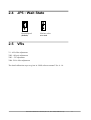
2.2
JP1 : Single-ended/Differential
Analog Input Type Select
Analog input are
differential type
(16 channels max)
Analog input are
single-ended type
(32 channels max)
(default)
2.3
JP2 : IRQ Channel Selection
IRQ3
IRQ4
IRQ5
IRQ6
IRQ7
IRQ9
IRQ10
IRQ11
IRQ12
IRQ14
IRQ15
NC (default)
ISO-AD32 Hardware Manual(Ver.1.0, Feb/1998, IPH-012-10)
----
10
2.4
2.5
JP5 : Wait State
Normal Speed
ISA bus select
(default)
zero wait
VRs
V1 : AD offset adjustment
VR2 : AD gain adjustment
VR3 : -5V adjustment
VR4 : PGA offset adjustment
The detail calibration steps are given in “DOS software manual” Sec. 4.1.4.
ISO-AD32 Hardware Manual(Ver.1.0, Feb/1998, IPH-012-10)
----
11
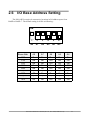
2.6
I/O Base Address Setting
The ISO-AD32 occupies 8 consecutive locations in I/O address space from
BASE to BASE+7. The default setting is 0x220 as following :
ON
1
2
3
4
5
6
A8
A7
A6
A5
A4
NC
Base Addr
A8
A7
A6
A5
A4
200
210
220
230
250
:
300
:
3F0
On
On
On
On
On
:
Off
:
Off
On
On
On
On
On
:
On
:
Off
On
On
On
On
Off
:
On
:
Off
On
On
Off
Off
On
:
On
:
Off
On
Off
On
Off
Off
:
On
:
Off
ISO-AD32 Hardware Manual(Ver.1.0, Feb/1998, IPH-012-10)
----
12
2.7
CN1 Connectors
Pin assignment for single-ended analog input
Pin
Name
Pin
Name
1
AI0
20
AI16
2
AI1
21
AI17
3
AI2
22
AI18
4
AI3
23
AI19
5
AI4
24
AI20
6
AI5
25
AI21
7
AI6
26
AI22
8
AI7
27
AI23
9
AI8
28
AI24
10
AI9
29
AI25
11
AI10
30
AI26
12
AI11
31
AI27
13
AI12
32
AI28
14
AI13
33
AI29
15
AI14
34
AI30
16
AI15
35
AI31
17
Analog Common
36
Analog GND
18
Digital +5V output
37
Digital GND
19 External Trigger Input
ISO-AD32 Hardware Manual(Ver.1.0, Feb/1998, IPH-012-10)
----
13
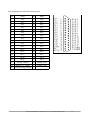
Pin assignment for differential analog input
Pin
Name
Pin
Name
1
AI0+
20
AI0-
2
AI1+
21
AI1-
3
AI2+
22
AI2-
4
AI3+
23
AI3-
5
AI4+
24
AI4-
6
AI5+
25
AI5-
7
AI6+
26
AI6-
8
AI7+
27
AI7-
9
AI8+
28
AI8-
10
AI9+
29
AI9-
11
AI10+
30
AI10-
12
AI11+
31
AI11-
13
AI12+
32
AI12-
14
AI13+
33
AI13-
15
AI14+
34
AI14-
16
AI15+
35
AI15-
17
Analog Cmmon
36
Analog GND
18
Digital +5V output
37
Digital GND
19 External Trigger Input
ISO-AD32 Hardware Manual(Ver.1.0, Feb/1998, IPH-012-10)
----
14
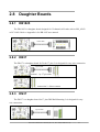
2.8
Daughter Boards
2.8.1
DB1825
The DB-1825 is a daughter board designed for 32 channels AD cards such as ISO_AD32
or PCI-1802. Refer to Appendix A for DB-1825 user manual.
37pin cable
2.8.2
DB37
The DB-37 is a daughter board for D-sub 37 pins. It is designed for easy wire connection.
37pin cable
connection 1 : by 37 pin cable
connection 2 : direct connect
2.8.3
DN37
The DN-37 is a daughter board for 37 pins DIN Rail Mounting. It is designed for easy
wire connection.
37pin cable
ISO-AD32 Hardware Manual(Ver.1.0, Feb/1998, IPH-012-10)
----
15
3.
3.1
Function Operation
AD Conversion Operation
The user do not need to know about the detail control of AD operations, the embedded
controller will handle the details.
3.1.1
The Configuration Code Table
ISO-AD32L Input Range Configuration Code Table
Bipolar/Unipolar Input Signal Range
Gain
Settling Time
Configuration Code
Bipolar
+/- 5V
1
3 us
0x00
Bipolar
+/- 2.5V
2
3 us
0x10
Bipolar
+/- 1.25V
4
3 us
0x20
Bipolar
+/- 0.625V
8
3 us
0x30
Bipolar
+/- 10V
0.5
3 us
0x80
Bipolar
+/- 5V
1
3 us
0x90
Bipolar
+/- 2.5V
2
3 us
0xA0
Bipolar
+/- 1.25V
4
3 us
0xB0
Unipolar
0V ~ 10V
1
3 us
0x00
Unipolar
0V ~ 5V
2
3 us
0x10
Unipolar
0V ~ 2.5V
4
3 us
0x20
Unipolar
0V ~ 1.25V
8
3 us
0x30
ISO-AD32 Hardware Manual(Ver.1.0, Feb/1998, IPH-012-10)
----
16
ISO-AD32H Input Range Configuration Code Table
Bipolar/Unipolar Input Signal Range
Gain
Settling Time
Configuration Code
Bipolar
+/- 5V
1
23 us
0x00
Bipolar
+/- 0.5V
10
28 us
0x10
Bipolar
+/- 0.05V
100
140 us
0x20
Bipolar
+/- 0.005V
1000
1300 us
0x30
Bipolar
+/- 10V
0.5
23 us
0x80
Bipolar
+/- 1V
5
28 us
0x90
Bipolar
+/- 0.1V
50
140 us
0xA0
Bipolar
+/- 0.01V
500
1300 us
0xB0
Unipolar
0V ~ 10V
1
23 us
0x00
Unipolar
0V ~ 1V
10
28 us
0x10
Unipolar
0V ~ 0.1V
100
140 us
0x20
Unipolar
0V ~ 0.01V
1000
1300 us
0x30
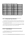
3.1.2
Analog Input Type Selection
The analog input signal can be single-ended or differential. If select single-ended, there can
be 32 channels max. If select differential, there can be only 16 channels max. But some signal
can not be connected as single-ended input, such as thermocouple couple sensor. Refer to Sec
3.7 for analog signal input type selection.
The embedded control can read back the JP1 setting. If the software tell the embedded
controller to perform single-ended operation and the JP1 in the wrong setting, the embedded
controller will return a error code. Refer to software manual for details.
3.1.2.1
Unipolar/Bipolar
If the analog input signal is unipolar, you can measure this signal with bipolar setting
(this will reduce resolution only). If the analog input is bipolar, you must select bipolar
configuration code to measure this signal.
ISO-AD32 Hardware Manual(Ver.1.0, Feb/1998, IPH-012-10)
----
17
3.1.3
The Input Signal Range
If the input range of analog signal is +/- 1V, you can measure this signal wih +/-10V, +/5V, +/-2.5V and +/- 1.25V configuration code setting. The only difference is the resolution.
The resolution of +/- 2.5V is 4 times higher than in +/- 10V setting. Select the correct
configuration code will get the best resolution.
3.1.3.1
The Gain Factor
The analog input signal will be amplified by gain factor. If the user wish to compute the
real value, the AD data must divided with the gain factor. The general real value computation
functions is given as follows:
double AD32L_ComputeRealValueBipolar(WORD wAdConfig, WORD wAdHex)
{
WORD wZERO=2048;
double dfMAX, dfVal;
switch (wAdConfig)
{
case 0x00 : dMAX=5.0;
break;
case 0x10 : dMAX=2.5;
break;
case 0x20 : dfMAX=1.25; break;
case 0x30 : dfMAX=0.625; break;
case 0x80 : dfMAX=10.0; break;
case 0x90 : dfMAX=5.0;
break;
case 0xA0 : dfMAX=2.5;
break;
case 0xB0 : dfMAX=1.25; break;
default : return(ConfigCodeError);;
}
dfVal=(((double)(wAdHex)-wZERO)/2048.0)*dfMAX;
return(dfVal);
}
ISO-AD32 Hardware Manual(Ver.1.0, Feb/1998, IPH-012-10)
----
18
double AD32L_ComputeRealValueUnipolar(WORD wAdConfig, WORD wAdHex)
{
WORD wZERO=0;
double dfMAX, dfVal;
switch (wAdConfig)
{
case 0x00 : dMAX=10.0;
break;
case 0x10 : dMAX=5.0;
break;
case 0x20 : dfMAX=2.5;
break;
case 0x30 : dfMAX=1.25; break;
default : return(ConfigCodeError);;
}
dfVal=(((double)(wAdHex)-wZERO)/2048.0)*dfMAX;
return(dfVal);
}
double AD32H_ComputeRealValueBipolar(WORD wAdConfig, WORD wAdHex)
{
WORD wZERO=2048;
double dfMAX, dfVal;
switch (wAdConfig)
{
case 0x00 : dMAX=5.0;
break;
case 0x10 : dMAX=0.5;
break;
case 0x20 : dfMAX=0.05; break;
case 0x30 : dfMAX=0.005; break;
case 0x80 : dfMAX=10.0; break;
case 0x90 : dfMAX=1.0;
break;
case 0xA0 : dfMAX=0.1;
break;
case 0xB0 : dfMAX=0.01; break;
default : return(ConfigCodeError);;
}
dfVal=(((double)(wAdHex)-wZERO)/2048.0)*dfMAX;
return(dfVal);
}
ISO-AD32 Hardware Manual(Ver.1.0, Feb/1998, IPH-012-10)
----
19
double AD32H_ComputeRealValueUnipolar(WORD wAdConfig, WORD wAdHex)
{
WORD wZERO=0;
double dfMAX, dfVal;
switch (wAdConfig)
{
case 0x00 : dMAX=10.0;
break;
case 0x10 : dMAX=1.0;
break;
case 0x20 : dfMAX=0.1;
break;
case 0x30 : dfMAX=0.01; break;
default : return(ConfigCodeError);;
}
dfVal=(((double)(wAdHex)-wZERO)/2048.0)*dfMAX;
return(dfVal);
}
3.1.3.2
If the
The Settling Time
channel number or gain factor is change, the hardware need
extra time for signal ready. This is called the settling time. This limitation will apply both to
the Fixed-channel mode and MagicScan mode AD conversions. So the user must take care to
avoid the settling error. Refer to “DOS software manual” Sec. 3.6.
3.1.3.3
The
How to Delay the Settling Time
software driver can auto delay the settling time. Refer to “DOS
software manual” Sec. 3.6 for fixed-channel AD conversion.
It is no need to delay the settling time in the channel-scan mode AD conversion
ISO-AD32 Hardware Manual(Ver.1.0, Feb/1998, IPH-012-10)
----
20
3.1.4
The AD Conversion Mode
The AD operation can be
fixed-channel mode or channel-scan
mode.
In the fixed-channel mode, the AD operation will fix at one channel until the change
channel command is received. Refer to “DOS software manual” Sec3.6, Sec. 3.7, Sec. 3.9,
Sec. 3.10 for details.
In the channel scan mode, the embedded controller will auto scan and change gain. The
scan sequence and gain for each channel can be programmable. Refer to the software
manual for details. Refer to “DOS software manual” Sec3.16, Sec. 3.17, Sec. 3.18 for details.
ISO-AD32 Hardware Manual(Ver.1.0, Feb/1998, IPH-012-10)
----
21
3.1.5
The Channel Scan Circular_Scan_Queue
The channel scan controller equips with a circular
queue for scan sequence control.
The scan sequence is one by one and repeatable with the limitation of maximum 32 channels.
So the following scan sequence are all validate :
One channel scan
0
two channel scan, scan sequence=010101
0
1
1
0
0
0
1
2
3
Three channel scan : 123123123
2
5
1
Three channel scan : 251251251
2
5
2
Three channel scan : 252252252
2
2
2
Three channel scan : 222222222
two channel scan, scan sequence=101010
two channel scan, scan sequence=000000
ISO-AD32 Hardware Manual(Ver.1.0, Feb/1998, IPH-012-10)
----
22
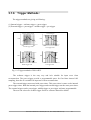
3.1.6
Trigger Methods :
The trigger methods are giving as following:
(1) Internal trigger = software trigger + pacer trigger
(2) External trigger = post-trigger + middle-trigger + pre-trigger
Pacer or software trigger
External trigger
CHn
CHn
t
Start
End
Internal trigger mode
Start
End
t
Post-trigger mode
External trigger
External trigger
CHn
CHn
N
Start
End
t
Middle-trigger mode
Start
End
t
Pre-trigger mode
Fig 1-2: Trigger methods of ISO-AD32.
The software trigger is the easy way and isn’t suitable for input wave form
reconstruction. The pacer trigger provide a programmable pacer for fixed time interval AD
sampling, therefore it is suitable for input wave form reconstruction.
The external trigger must used with pacer timer. This pacer timer is same as the internal
pacer trigger timer. Both the internal pacer trigger and external trigger use the same pacer timer.
The external trigger can be post-trigger, middle trigger or pre-trigger software programmable.
The user can select one of these trigger. Refer to software manual for details.
ISO-AD32 Hardware Manual(Ver.1.0, Feb/1998, IPH-012-10)
----
23
3.2
Refer to
3.3
Refer to
Diagnostic Program
“ISO-AD32 DOS software manual” Chapter 4 for details.
Calibration
“ISO-AD32 DOS software manual” Sec 4.1.4 for details.
ISO-AD32 Hardware Manual(Ver.1.0, Feb/1998, IPH-012-10)
----
24
3.4
Analog Signal Connection
The ISO_AD32 can measure single-ended or differential type analog input signal. Some
analog signal can be measured in both of single-end or differential mode but some only can be
measured in one of the single-ended or differential mode. The user must decide which mode is
suitable for measurement.
In general, there are 3 different analog signal connection method as shown in Fig1 to Fig3.
The Fig1 is suitable for grounding source analog input signals. The Fig2 can measure more
channels than in the Fig1 but only suitable for large analog input signals. The Fig3 is suitable
for thermocouple and the Fig4 is suitable for floating source analog input signals.
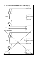
Note : In Fig3, the maximum common mode voltage between the analog input
source and the AGND is 70Vp-p, so the user must make sure that the input signal is
under specification first. If the common mode voltage is over 70Vp-p, the input
multiplexer will be damaged forever.
The simple way to select the input signal connection configuration is as below.
1.
2.
3.
4.
Grounding source input signal
select Fig1
Thermocouple input signal
select Fig3
Floating source input signal
select Fig4
If Vin > 0.1V and gain<=10 and need more channels
select Fig2
If the user can not make sure the characteristic of input signal, the test steps are given as
below:
1.
2.
3.
4.
Step1 : try Fig1 and record the measurement result
Step2 : try Fig4 and record the measurement result
Step3 : try Fig2 and record the measurement result
Compare the measurement result of step1,step2,step3 and
select the best one
ISO-AD32 Hardware Manual(Ver.1.0, Feb/1998, IPH-012-10)
----
25
1. FG1 : Connecting to grounding source input (Right way)
ISO_AD32
A/D CH0HI
Es1
A/D CH0LO
GND1
Analog Common
A/D CHnHI
Esn
A/D CHnLO
GNDn
Analog Common
FG1 : Wrong way
A/D CH0HI
Es1
A/D CH0LO
GND1
Analog Common
A/D CHnHI
Esn
A/D CHnLO
GNDn
Analog Common
ISO-AD32 Hardware Manual(Ver.1.0, Feb/1998, IPH-012-10)
----
26
FG2 : Connecting to singled-ended input configuration
ISO_AD32
A/D CH0
A/D CHn
Es
Analog Common
FG3 : connecting to thermocouple configuration
ISO_AD32
A/D CH0HI
A/D CH0LO
A/D CHnHI
A/D CHnLO
Analog Common
Note : If the input signal is not thermocouple, the user
Do not join LO to Analog
should use oscilloscope to measure common mode
voltage of Vin before connecting to ISO-AD32. Don’t use
voltage meter or multimeter.
Common at the computer
CAUTION : In Fig3, the maximum common mode voltage between the
analog input source and the AGND is 70Vp-p, so the user must make sure that the
input signal is under specification first. If the common mode voltage is over 70Vp-p, the
input multiplexer will be damaged forever.
ISO-AD32 Hardware Manual(Ver.1.0, Feb/1998, IPH-012-10)
----
27
FG4 : connecting to floating source configuration
ISO_AD32
A/D CH0HI
Es
A/D CH0LO
Analog Common
A/D CHnHI
Esn
A/D CHnLO
Analog Common
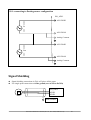
Signal Shielding
Signal shielding connections in Fig1 to Fig4 are all the same
Use single-point connection to frame ground (not AGND or DGND)
Vin
ISO_AD32
AGND
DGND
Frame Ground
ISO-AD32 Hardware Manual(Ver.1.0, Feb/1998, IPH-012-10)
----
28
Appendix A : The DB-1825 user manual
A.1 : PCB layout for connecting to ISO_AD32:
R
R
R
Acom 14-
14+ Acom 12-
12+ Acom 10-
10+ Acom 8-
8+
Acom Acom Dgnd
Acom 15-
15+ Acom 13-
13+ Acom 11-
11+ Acom 9-
9+
+5V Agnd Etrg
R
R
R
R
Acom 7-
7+ Acom 5-
5+
Acom 3-
3+
Acom 1-
1+
Acom 6-
6+ Acom 4-
4+
Acom 2-
2+
Acom 0-
0+
R
R
R
R
Acom 30
14
Acom 28
12
Acom 26
10
Acom 24
8
Acom Acom Dgnd
Acom 31
15
Acom 29
13
Acom 27
11
Acom 25
9
+5V Agnd Etrg
R
R
R
R
Acom 23
7
Acom 21
5
Acom 19
3
Acom 17
1
Acom 22
6
Acom 20
4
Acom 18
2
Acom 16
0
R
R
Pin assignment of D1 same as CN1 of ISO-AD32
Pin assignment of D2 same as CN1 of DB-889D
ISO-AD32 Hardware Manual(Ver.1.0, Feb/1998, IPH-012-10)
----
29
D2 : for connecting to DB-889D
D1 : for connecting to ISO-AD32
for single-ended input (R=0 ohm)
DB-1825
R
D2 : for connecting to DB-889D
D1 : for connecting to ISO-AD32
for differential input (R=0 ohm)
DB-1825
A.2 : PCB layout for connecting to PCI-1802:
R
R
R
Agnd 14-
14+ Agnd 12-
12+ Agnd 10-
10+ Agnd 8-
8+
Agnd Agnd Dgnd
Agnd 15-
15+ Agnd 13-
13+ Agnd 11-
11+ Agnd 9-
9+
DA1 DA2 Etrg
R
R
R
R
Agnd 7-
7+
Agnd 5-
5+
Agnd 3-
3+
Agnd 1-
1+
Agnd 6-
6+
Agnd 4-
4+
Agnd 2-
2+
Agnd 0-
0+
R
R
R
R
Agnd 30
14
Agnd 28
12
Agnd 26
10
Agnd 24
8
Agnd Agnd Dgnd
Agnd 31
15
Agnd 29
13
Agnd 27
11
Agnd 25
9
DA1 DA2 Etrg
R
R
R
R
Agnd 23
7
Agnd 21
5
Agnd 19
3
Agnd 17
1
Agnd 22
6
Agnd 20
4
Agnd 18
2
Agnd 16
0
R
R
Pin assignment of D1 same as CON3 of PCI-1802
Pin assignment of D2 same as CN1 of DB-889D
ISO-AD32 Hardware Manual(Ver.1.0, Feb/1998, IPH-012-10)
----
30
D2 : for connecting to DB-889D
D1 : for connecting to PCI-1802
for single-ended input (R=0 ohm)
DB-1825
R
D2 : for connecting to DB-889D
D1 : for connecting to PCI-1802
for differential input (R=0 ohm)
DB-1825
A.3 : connection to ISO-AD32
37pin cable
A.4 : connection to PCI-1802
37pin cable
A.5 : connection to PCI-1802 and multiple DB-889D(16 channels differential)
37pin cable
37pin cable
20 pins flat cable
ISO-AD32 Hardware Manual(Ver.1.0, Feb/1998, IPH-012-10)
----
31