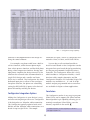
1
The Future of
EDITOR
Carlis Collins
[email protected]
408-879-4519
SENIOR DESIGNER
Jack Farage
BOARD OF ADVISORS
Dave Stieg
Andy Larg
Mike Seither
Pronto Creative
Logic Design...
W
ithin the next five years, programmable logic will be the
key technology for developing next generation products; within the
next ten years, programmable logic
devices (PLDs) will be used in virtually
every electronic product on the market.
These industry predictions are based on
a number of recent developments that
have forever changed the way electronic
systems are designed.
The old advantages of custom ASICs
are quickly being overcome by the new
advantages of programmable logic. Here
are some of the reasons why:
www.prontocreative.com
Xilinx, Inc.
2100 Logic Drive
San Jose, CA 95124-3450
Phone: 408-559-7778
FAX: 408-879-4780
©2000 Xilinx Inc.
All rights reserved.
Xcell is published quarterly. XILINX, the
Xilinx logo, and CoolRunner are registered
trademarks of Xilinx, Inc. Virtex,
LogiCORE, Spartan, SpartanXL, Alliance
Series, Foundation Series, CORE Generator,
Checkpoint Verification, TimeSpecs, Smart
IP, QPRO, SelectI /O, SelectI/O+, True DualPort, WebFITTER, WebPACK, Select RAM,
BlockRam, Xilinx Online, and all XC-prefix
products are trademarks, and The
Programmable Logic Company is a service
mark of Xilinx, Inc. Other brand or product
names are trademarks or registered trademarks of their respective owners.
The articles, information, and other materials included in this issue are provided
solely for the convenience of our readers.
Xilinx makes no warranties, express,
implied, statutory, or otherwise, and
accepts no liability with respect to any
such articles, information, or other materials or their use, and any use thereof is
solely at the risk of the user. Any person
or entity using such information in any
way releases and waives any claim it
might have against Xilinx for any loss,
damage, or expense caused thereby.
Very High Density, System-level
Devices - We now produce high performance FPGAs with advanced features
and up to 3.2 million system gates. Plus,
we have just announced our next generation 10-million gate architecture. With
devices this powerful and this dense you
are limited only by your imagination.
Very Low Power, Low-cost
Devices - Many new designs require
battery operation and low cost. Our Fast
Zero Power™ CPLDs are perfect for cell
phones, PDAs and other power sensitive
applications. Our Spartan FPGAs already
give you 100K gates for less than
$10.00, and higher density, lower cost
FPGAs are on the way. Power and price
are no longer an issue with PLDs.
Intellectual Property - The fastest
and surest way to get your PLD-based
product to market is to use proven
2
designs, either those created in-house or
by third party suppliers. There is already
a wealth of IP, and many new designs
are being introduced every day. IP significantly reduces your development time
and your risk.
Highly Efficient Development
Tools - Speed is critical. Not only do
you want the fastest design you can create, but you want to complete that
design with the least possible risk and
effort. The currently available development tools from Xilinx allow you to
quickly develop your designs in many
different ways, with multiple developers
located in different places. These tools
are fast, efficient, and easy to use; and
they are constantly improving.
Field Upgradeability - With the
current Xilinx device and software technologies you can create designs that are
easily changed, in the field, over any
network, right at your customers’
premises. The possibilities are enormous, and the advantages are overwhelming; this cannot be duplicated
with any other technology. Now, just like
software, your hardware can easily
change to meet the demands of the
marketplace.
With programmable logic you not
only get the fastest and easiest way to
create next-generation systems, you
also get significant advantages that cannot be offered by fixed logic ASICs; there
is no better way to create value.
Inside This Issue:
View from the Top
COVER STORY
GoAhead Software—A complete system
for managing and remotely upgrading
your FPGA designs in the field.
5
The Promise of Field Upgradable
Systems . . . . . . . . . . . . . . . . . . . . .4
Cover Story
Creating Field Upgradable
Hardware Systems . . . . . . . . . . . . . .5
CoolRunner CPLDs
Fast Zero Power (FZP)Technology
.10
XPLA3 Development Kit . . . . . . . . .12
Implementing a 16B/20B Encoder/
Decoder in a CoolRunner CPLD . . .14
COOLRUNNER
The CoolRunner XPLA3 Development Kit
is the perfect way to get started using
the most efficient, low power CPLD on
the market.
12
Virtex
New Virtex-EM FPGAs Over
1 Mbits of RAM . . . . . . . . . . . . . . .15
Software
Xilinx Development Systems . . . . .16
On-chip, Real-time Logic Analysis .19
JTAG Programmer . . . . . . . . . . . . .22
Architecural Synthesis from
Behavioral C Code . . . . . . . . . . . . .23
JTAG
Connection
SOFTWARE
Xilinx Software R&D delivers new version
3.1i software tools that empower you to
maximize your productivity, while leveraging your creativity.
16
Cores
Data Encryption Cores . . . . . . . . . .26
Image Compression Cores . . . . . . .28
Using an 8051 Core and QPRO
. . .30
Support Products
A High Speed Platform for Dynamically Reconfigurable Logic . . . . . . .33
New PCI 64/66 Design Kit . . . . . . .34
SUPPORT PRODUCTS
New PCI Development Kit includes a prototyping board, driver development tools,
and reference designs.
34
Mass Storage for Xilinx FPGA
. . . .37
Applications
Using the Virtex Look Up Tables . . .40
Efficient Debugging Using PROBE
.44
Control Virtex Design Optimzation 47
Success Stories
A New Internet Protocol Service
Switch Uses FPGAs . . . . . . . . . . . .49
REFERENCE
Availability guides for Virtex FPGAs,
Spartan FPGAs, XC9500 and CoolRunner
CPLDs, QPRO FPGAs, PROMs, and
Configuration Solutions.
57
FPGAs for a Reconfigurable Image
Processing Module . . . . . . . . . . . .51
Columns/Reference
Electronic Distribution . . . . . . . . .54
Trade Shows . . . . . . . . . . . . . . . .55
Customer Education . . . . . . . . . . .56
Virtex Reference Guide . . . . . . . . .57
Spartan Reference Guide . . . . . . .58
CPLD Reference Guide . . . . . . . . .59
QPRO Reference Guide
www.xilinx.com
For A FREE
Subscription
To The Xcell
Journal
E-mail your request to: [email protected],
please be sure to include:
1. Your full name and
mailing address
2. Your title
4. Your e-mail address
5. Is this new subscription
or a subscription renewal?
3. The name of your company
3
. . . . . . . .60
PROM Reference Guide . . . . . . . .61
Configuration Solutions . . . . . . . .62
View from the Top
The
Promise of
Field Upgradable Systems
by Wim Roelandts, President and CEO, Xilinx
ne of the most exciting devel-
O
munications or microprocessor interface, making the
opments in our industry is the
addition of remote field update capability a simple
increasing shift toward using
matter. If you consider doing remote updates during
networks, including the Internet, to
the initial specification and design process, your sys-
remotely upgrade the digital equipment
tems can easily reap all the benefits of being updated
that is already installed at a customer’s
remotely.
location, anywhere in the world, and beyond.
Remote upgradability significantly increases the
Updating software remotely, with new enhance-
useful lifetime of a system. The ability to add new
ments and bug fixes, is a common practice. However,
hardware features and fix existing ones without send-
remotely updating hardware may appear to be more
ing a technician out to the field can add up to consid-
challenging because hardware is typically a fixed
erable maintenance and support savings over the
entity that is updated by manually replacing circuit
entire life of the system. Imagine the implications for
boards. Now, with our current FPGA families and the
satellite-based communications equipment.
Xilinx Online software technologies, doing automatic,
Remotely upgradeable systems can also provide
remote hardware upgrades is not only a reality, it is
new revenue prospects. After the initial product is
becoming a necessity in many new applications.
released, you can develop new hardware features
Researchers have been investigating this concept
then sell and distribute those features to existing cus-
for years, and a few forward looking companies have
tomers just as software developers do today. Or a
already deployed FPGA-based remotely reconfigurable
standard “off-the-shelf” application can be developed
products. IBM, for example, currently markets an ATM
so features can be swapped in and out depending on
switch whose FPGA-based logic can be changed over
what the end-user purchases or needs.
the network to bring it into accord with the latest
Any system that has some type of connectivity to
changes in the ATM standard. A number of Xilinx cus-
the “outside world” could potentially benefit from
tomers, including large communications companies
being designed to support field updates. Typical prod-
building the next generation of WCDMA wireless sys-
ucts include network appliances, set-top boxes, secu-
tems, are very interested in the idea, and a few are
rity systems, network equipment, cellular base sta-
well along the way with major designs efforts.
tions, and satellite communications systems. Other
The advantages of this new possibility are enor-
likely applications are HDTV, video and image pro-
mous. For example, the ability to remotely update
cessing, encryption, military communications, surveil-
hardware with new features or the latest bug fix can
lance, radar, and sonar.
accelerate your time-to-market, extend the useful life
Clearly, electronic equipment manufacturers who
of existing systems, and significantly cut production,
begin to think about the benefits of remote hardware
maintenance, and support costs. Many of today’s sys-
upgrades today will be the ones who lead their mar-
tems already come with some form of built-in com-
kets in the not-to-distant future.
4
Cover Story
Creating
FIELD UPGRADABLE
Hardware Systems Using
Enabling Technology from
GoAhead
Software
A complete system for managing and
remotely upgrading your FPGA
designs in the field.
by Greg Brown, Xilinx Software Product Manager for Internet Applications, [email protected]
and by Mike Akers, GoAhead Software FieldUpgrader Product Manager, [email protected]
F
or many years designers have been using
Xilinx programmable logic devices (PLDs)
to reap the benefits of fast time-to-market.
Now, a second major advantage is made possible through the partnership of GoAhead
Software and Xilinx—the ability to upgrade your
designs via a network after they have been
deployed in the field. This can result in dramatic
field service cost savings and it helps “futureproof” your product.
GoAhead FieldUpgrader
The GoAhead FieldUpgrader software consists of
three parts:
• GoAhead DeviceStudio™ - a development
environment used to create the UpgradeAgent
software.
• GoAhead UpgradeAgent™ - the software
that is embedded in the target device. Each
agent is unique to the particular operating
system that is resident on the target system.
The target system containing the
UpgradeAgent polls the UpgradeServer at regular pre-determined intervals to look for
FPGA upgrades. When an upgrade is available, the device downloads the upgrade to a
predetermined storage location. This process
is illustrated in Figure 1.
The Solution for Field Upgrading
The new Xilinx and GoAhead Software solution
combines the GoAhead commercial software
(GoAhead FieldUpgrader™) with the Xilinx
Internet Reconfigurable Logic methodology
(IRL™) to provide the enabling technology to
help you create and manage field upgradable
systems. This technology provides the backbone
for network-based system designs as well as the
delivery mechanisms to successfully deploy
upgradable products.
• GoAhead UpgradeServer™ - used to create
and publish upgrades and is usually located
on a server at the manufacturer’s site. When
the need for an FPGA upgrade arises, the
manufacturer publishes the upgrade with
UpgradeServer.
5
Device
Manufacturer
Device initiated request
Upgrade request response
Request for payload
Payload
Response
Figure 1 - The remote upgrade process.
Data Security and Integrity
detects a checksum error, it discards that chunk
and re-fetches it from the upgrade server. Once
all of the chunks have been downloaded, the
device reconstructs the payload and performs
the higher-level data integrity check.
To upgrade devices over a network, it is critical
that the devices only accept upgrades from the
authorized, designated server. It is also important to ensure that the upgrade payload is not
modified or corrupted. GoAhead FieldUpgrader
and the UpgradeServer use a variety of techniques to authenticate the upgrade and prevent
modifications along the way.
Data integrity is also checked during the
actual programming of the Xilinx FPGAs; there is
a CRC checksum built into the programming
step.
Fault Tolerance
GoAhead FieldUpgrader uses the Digital
Signature Standard (DSS), which specifies a
The UpgradeAgent is fault tolerant during the
transmission of the upgrade. The Agent knows
the contents of the payload based on the manifest list and will re-initiate the upgrade to fetch
any missing chunks if the connection with the
server is lost.
Digital Signature Algorithm (DSA). The DSA provides the capability to generate and verify signatures using public and private keys. In addition,
the device-initiated approach provides built-in
security; the device does not accept externally
initiated upgrades. The location and port of the
upgrade server is configured into the target
device and the device will only allow upgrades
from this designated upgrade server. This
method ensures that the upgrade payload
received at the target device matches the original upgrade payload published at the upgrade
server and guarantees that the message was not
modified en-route to the device.
The application of the upgrade to the Xilinx
device can also be made fault tolerant in the system architecture, which is shown in Figure 4.
The concept uses redundant non-volatile storage
areas—one to hold the current, known good system, and the other to hold the upgrade. The system can always fall back to the known good
configuration if there are any issues associated
with upgrading the system.
The payload of the upgrade is broken into
smaller chunks to make the transfer more efficient and re-startable. GoAhead FieldUpgrader
calculates a 32-bit CRC checksum for each of
these individual chunks. If the target device
Flexibility By Design - Pull or Push?
There are some applications that may require a
“push” method of upgrading. The term “push”
6
entails the directing and initializing of upgrades
from a central server. There are cases or management decisions that may dictate this alternative to providing upgrades.
• File system (optional for VxWorks).
• Provision of the main software module’s C
source code (main.c) and a linkable library to
enable the integration of the UpgradeAgent
into custom applications.
The FieldUpgrader software primarily uses a
device-initiated or “pull” methodology. However,
it was developed to be flexible as well, and can
be enhanced to allow a “push” methodology. At
a pre-determined time, the UpgradeAgent may
simply open a communications port to listen for
“hello” messages that are broadcasted or multicasted from the UpgradeServer. If the
UpgradeAgent responds after verification, the
UpgradeServer sends a request packet to the
system to begin the upgrade process. The
UpgradeAgent then makes the request for an
upgrade from the secure UpgradeServer. This
methodology solves the problems associated
with firewalls and security. The requests may
pass through firewalls and the device port
remains open for only the specified upgrade
period.
• Support for embedded JavaScript calls with
the ability to:
-
Control the upgrade process
-
Load and call C functions to extend functionality
-
Send additional request data to GoAhead
UpgradeServer
-
Access GoAhead UpgradeAgent environment variables
Demonstration Design
The demonstration design utilizes the GoAhead
FieldUpgrader to upgrade a Xilinx XCS05 Spartan
FPGA, which is connected to a popular embedded system—a single-board computer running
Wind River’s VxWorks® real-time operating system. This type of system exists in many applications and environments from industrial control
stations to remote monitoring systems. Figure 2
shows a diagram of the system.
System Support
GoAhead FieldUpgrader supports the following
platforms:
• GoAhead UpgradeServer, GoAhead
DeviceStudio:
Remote System
Windows NT4.0, Linux 2.2, Microsoft
Internet Explorer 4.x or greater, Netscape
4.x or greater
• GoAhead UpgradeAgent:
Wind River VxWorks 5.3.1 or greater (x86,
PowerPC, ARM, MIPS), Windows 95/98/NT
(x86, PowerPC), Windows CE (x86, Hitachi
SH) or Linux 2.2 (x86)
Parallel
Cable
TCP/IP
Field Upgrader
Server System
Agent System
(VxWorks)
(Windows NT 4.0)
Single board
486 Computer
Payload Package
Field Upgrader Agent
upgrade .js
xiprog.o
test.bit
(includes javascript
interpreter)
Monitor
Runs upgrade.js
Hard disk
Dynamically loads xiprog.o
into VxWorks
Programs XCS05
with test bit
The key requirements of the UpgradeAgent
are:
Xilinx Demo Board
(Spartan XCS05)
Power Supply
• TCP/IP stack and connection.
Figure 2 - Demonstration system.
• Real-time clock.
7
This demonstration system includes the following components:
UpgradeServer: one to upgrade the bitstream
and one to downgrade to the original bitstream.
This enables the system to toggle between the
two FPGA configurations.
Processor - The processor is a single-board,
Intel 486-based system. The board has 2MB of
RAM, integrated VGA controller, an IDE controller, and a parallel interface. A hard disk is
used for non-volatile storage other than the
BIOS.
UpgradeServer - The UpgradeServer is running
on a laptop PC using Microsoft NT4.0. It waits
until the UpgradeAgent on the VxWorks system
contacts it and requests an upgrade. If there is
an available upgrade, the server sends the
upgrade payload to the VxWorks system across
the TCP/IP network.
Xilinx demonstration board - This board has
two devices on it: an XC3020A and a Spartan
XS05. The Spartan XS05 is a 5000 system gate
FPGA that is used in high volume, low-cost
applications.
Demonstration Upgrade Process
The upgrade process used in the demonstration
design is illustrated by the flow diagram in
Figure 3.
Xilinx Parallel Cable III - This cable runs
between the single board computer and the
Xilinx demonstration board. This cable is used to
provide the communication between the computer system and the Xilinx FPGA.
Demonstration System Upgrade Process
VxWorks programs the
XS05 through parallel
port using bit file on disk
Wind River VxWorks - The VxWorks® RealTime Operating System (RTOS) from Wind River
Systems is the most widely used RTOS for
embedded systems.
Upgrade Agent waits
on event schedule
Upgrade Agent build
HTTP request
Upgrade Agent sends
request to Upgrade Server
Upgrade Agent runs
upgrade.js javascript
Upgrade Agent unarchives a payload
(Xiprog.o, upgrade.js, test.bit)
Upgrade Agent verifies
payload
Upgrade Agent rebuilds
archive file
The GoAhead UpgradeAgent - This is a realtime embedded application that uses VxWorks’
dynamic loading capability to load and execute
other real-time embedded applications. In the
demonstration design, this feature of VxWorks is
used to dynamically load the object code that
No
No
Upgrade Server
Operations
programs the Xilinx FPGA. This was strictly an
architectural choice. An alternative and equally
valid approach is to have the object code that
programs the Xilinx device be resident on the
VxWorks system and not include it as part of the
upgrade process, or use a combination of the
two approaches.
Is
Upgrade
Available
?
Is
Policy
Valid
?
Manifest is sent to
Upgrade Agent
All
Chunks
received
?
Is
Chunk
Valid
?
Upgrade Agent fetches
upgrade chunk to disk
Figure 3 - Demonstration system upgrade process.
Building a Commercial System
There are several potential field upgradable
architectures to which the concepts presented
here apply. However, only one is described
here—the single board computer running an
RTOS with programmable logic, as shown in
Figure 4.
The UpgradeAgent is configured to poll the
UpgradeServer once each minute to check for
upgrades. When one exists, it downloads the
upgrade payload and executes the instructions
included in the payload. For demonstration purposes, two payloads are published on the
In Figure 4, the processor must be one supported by the GoAhead UpgradeAgent. This can
8
Storage 2 is ready to contain the next upgrade.
Possible selections for the non-volatile memory
are EEPROMS, FLASH memory cards, or the
Xilinx XC18V00 in-system programmable configuration PROMs. (See page 62.)
Basic Architecture
Xilinx
FPGA/CPLD
I/O
Processor
Non-Volatile
Storage 1
Non-Volatile
Storage 1
Software
Non-Volatile
Storage 3
There are two basic software components that
need to be written for the target processor architecture:
Figure 4 - Basic system architecture.
be either an Intel X86 (or compatible), PowerPC,
ARM, or MIPS processor running VxWorks as the
RTOS (or a supported Microsoft Windows or
Linux configuration as previously listed).
• Firmware to copy the Xilinx programming file
to non-volatile storage.
• Firmware to program the FPGA.
Another approach is to use the Java programming language either with the firmware or
as a complete application (Xilinx supplies a Java
API for the Boundary Scan configuration mode).
A Java application can therefore be written (and
called by the UpgradeAgent) to program the
FPGA. On Windows platforms, there are several
Java run-time engines (the virtual machine)
available. On a VxWorks platform, the application would need to be developed using Personal
JWorks™ from Wind River.
The non-volatile storage can be divided into
three functions:
• Processor Program Memory (Non-Volatile
Storage 1) - contains firmware for the microprocessor.
• FPGA Configuration Storage (Non-Volatile
Storage 2) - contains configuration data for
the FPGA. The system can be designed so that
this storage area contains the initial configuration data.
• FPGA Configuration Storage (Non-Volatile
Storage 3) - contains configuration data for
the FPGA. The system can be designed so that
this storage area contains the first upgrade
configuration data.
Conclusion
The purpose of the GoAhead and Xilinx partnership is to provide the enabling technology and
solutions for a variety of field upgradable systems. GoAhead FieldUpgrader provides the management, deployment, communications, and
security backbone, while Xilinx provides reconfigurable hardware devices and programming
technologies. Together, you have the building
blocks needed to enable the rapid development
and deployment of a new generation of costsaving, life-extending, field-upgradable systems.
The system should be designed to always
have a last known-good configuration for the
FPGA. This is handled by the redundancy of the
Non-Volatile Storage 2 and Non-Volatile Storage
3. In a usual sequence of events, the FPGA will
be initially configured from Non-Volatile Storage
2. When an upgrade is requested, it is downloaded into Non-Volatile Storage 3. The FPGA is
then reconfigured from this location. The program controlling the programming of the FPGA
then switches the functions of these two storage
areas as Non-Volatile Storage 3 is now the
known-good configuration and Non-Volatile
For more information regarding how the Spartan-II family addresses traditional ASIC and ASSP designs, please see the article on page 49.
For more information see: www.xilinx.com/xilinxonline/
partners/goaheadhome.htm
9
Technology Update - CoolRunner
0
Fast Zero Power
(FZP) Technology
How CoolRunner CPLDs Minimize System Current Demand
CoolRunner CPLDs require very little power yet
operate at very high speeds—here’s how.
by Ron Cline, Director of CoolRunner Product Development, Xilinx, Inc., [email protected]
I
MUXs are programmed using RAM-based configuration bits.
n traditional CPLD architectures, including
the XC9500 series, the circuits that propagate
logic-level transitions in the product-term
array are derived from the original (old) bipolar
PLD designs. These older designs use sense
amplifiers at the end of each bit line in the product-term array to achieve fast propagation
delays. Because CPLD product terms cannot be
decoded (as with memory locations in an
EPROM, for example) there must be a sense
amplifier for each individual product-term. These
sense amplifiers must be continuously operational, and will draw continuous supply current
even when not switching.
The full CMOS AND gate shown in Figure 1
has a delay of under 0.5 nsec, including the
delay of the input MUXs.
The CoolRunner Design Technique
Figure 1 - CoolRunner Fast Zero Power AND gate.
The Xilinx CoolRunner design uses an innovative
method for implementing the product-term
array. Rather than employing sense amplifiers (a
bipolar-style circuit), CoolRunner CPLDs use true
CMOS circuitry. In the CoolRunner Fast Zero
Power (FZPTM ) approach represented in Figure
1, the AND gates in the product-term array are
implemented using configurable multiplexers
(MUXs) attached to the inputs of normal CMOS
NAND gates. Each MUX selects an input, it’s
complement, or Vcc (don’t care state.) These
I0
I1
Output = I
0
&I
1
&I
2
&I
3
I2
I3
A four input ‘AND’ function demonstrates how
the product term is implemented with full-CMOS
gates in the CoolRunner CPLDs.
Figure 2 - Representation of a 4-input product-term
using the CoolRunner FZP design technique.
10
I0
Output = I
0
&I
1
&I
2
&I
3
&I
4
&I
5
&I
6
&
I1
I2
I3
I4
I5
I6
I7
The previous example, expanded to implement an
eight-input AND function.
Figure 3 - Expanding the number of inputs.
Wider AND gates are built using a deMorgan
tree, as shown in Figure 2. Doubling the input
width simply requires the replacement of the
inverter in Figure 1 with a 2-input NOR gate.
This increases the total delay by less than 0.1
nsec.
This design technique can be extended for
wider widths, as shown in Figure 3 which shows
a re-doubling to eight inputs, at an additional
delay penalty of less than 0.2 nsec for the NAND
gate plus inverter. The inverter can be replaced
with a two-input NOR gate to enable a productterm width of 16 inputs (at an incremental delay
penalty of 0.1 nsec.).
As you can see, the delay penalty per additional input actually decreases as the number of
inputs into each product-term increases. This is
in contrast to the traditional sense amplifier
approach, where the delay increases linearly as
product-term input width is increased.
The gate tree implementation distributes the
capacitance at each product-term, so this capacitance is no longer lumped on a single node.
Furthermore, the switching current behaves in a
manner similar to that of random logic in a gate
array; the static current for each gate is small-
about 1 picoamp (pA). The total instantaneous
dynamic current is also small, because only the
gates in one path of the tree can switch, and
these gates switch in succession rather than all
at once.
Conclusion
The advantages of CoolRunner FZP CPLDs are
numerous. Total standby current is under 100
microamps—at least 1000 times less than that
exhibited by CPLDs using sense amplifiers. Total
dynamic power is also decreased, relative to
existing CPLDs, by as much as 70% for a device
whose logic is fully populated with 16-bit counters operating at 50 MHz. Best of all, these
power savings are realized with little impact on
performance and with no cumbersome powerdown circuitry.
Because power consumption is so low, chipscale packaging options, once considered impossible due to thermal limits, are now offered. As a
result, FZP technology is a key technology for
CPLDs because it enables very low-power, highperformance applications.
11
New Products - Development Tools
60µA
CoolRunner XPLA3
Development Kit
Draws Only
The CoolRunner XPLA3 Development Kit, from Xilinx and Insight
Electronics, is the perfect way to get started using the most efficient, low
power CPLD on the market.
by John Hubbard, Application Engineer, Xilinx, Inc.,
[email protected]
X
ilinx and Insight Electronics have jointly
developed a low power demonstration
board that allows you to easily experiment with the new CoolRunner XPLA3 architecture, using In System Programming (ISP) to configure the device. With this board, and the free
Xilinx PC-ISP3 Programmer software, you can
immediately begin configuring a CoolRunner
XPLA3 device with your custom design, directly
from your PC. If you need a little help getting
started, you can get the XPLA3 Demo Board
User’s Manual or the VHDL/Verilog tutorial from
the Xilinx Application Note website.
Figure 1 - The XPLA3
CoolRunner family.
down mode and is the only CPLD family delivering both high performance and ultra low power
consumption.
The XPLA3 CoolRunner family (Figure 1) has
the lowest power consumption of any CPLD family on the market. The entire CoolRunner XPLA3
Development Board, with its pre-programmed
“CoolrunnEr” scrolling marquee pattern, draws
only 60 µA. Since the board contains other components that also draw current, such as the onboard low power oscillator and LCD, the
CoolRunner CPLD actually draws less than
60 µA. Because the CoolRunner product line
requires so little power, it does not need a power
12
Key Features
The development board, shown in Figure 2, is
designed to demonstrate the low power requirements and the advanced features of the
CoolRunner architecture. The board uses the
Xilinx XCR3256XL, a 256-macrocell device in a
TQ144 package, which can be programmed via
the JTAG ISP port using the provided Xilinx
Figure 2 - The CoolRunner XPLA3 Development Kit uses
only 60 µa (powered here by six grapefruit).
Parallel Download Cable III; any JEDEC file that
targets the XCR3256XL can be downloaded.
To power the board you can use either:
• A 3.3V user regulated input.
• A 10.0V maximum input, regulated to 3.3V
using the on-board regulator.
• A 6.0V AC adapter input regulated to 3.3V
using the on-board regulator. This AC adapter
is included with the CoolRunner XPLA3
Development Kit.
Two clock sources are available to the
CoolRunner CPLD:
visually verify your design; it can be disconnected from the device if you choose. Control
pins are also included so you can easily implement the Xilinx Watch Tutorial which is available
for download from http://www.xilinx.com/
apps/epld.htm#tutorials.
Conclusion
You can quickly and easily become an XPLA3
CoolRunner guru by using the CoolRunner
XPLA3 Development Kit; and it’s available today
from Insight Electronics.
• The on-board, low power 32.768 kHz oscillator.
Order the CoolRunner XPLA3 Development Kit from the Insight website
at: http://www.insight-electronics.com/xcellence/scalable/kit/.
The part number is DS-XPLA3-PAK and the price is $95.00.
• Any external clock source with an impedance
of 50 ohms (to match the 50 ohm on-board
trace impedance).
Download the free PC-ISP3 Programmer software from the Xilinx
WebPACK website at http://www.xilinx.com/products/software/
webpowered.htm.
A prototyping area is also provided, and all
device I/Os are available for your prototype
either via the user access headers that surround
the CoolRunner device or via the 20 throughhole connections routed to specific I/Os. The
two-digit seven-segment LCD (shown in the
lower left corner of the board in Figure 2) is connected to specific I/Os so you can quickly and
Get the XPLA3 Demo Board User’s Manual or the VHDL/Verilog
tutorial from the Xilinx Application Note website at:
http://www.xilinx.com/apps/appsweb.htm.
Visit the XPLA3 CoolRunner website, for the latest CoolRunner
information, at: http://www.xilinx.com/products/xpla3.htm.
13
Products - CoolRunner CPLDs
Implementing a 16B/20B
Encoder/Decoder
in a CoolRunner CPLD
Here’s an overview of a complete design that you
can download from the Web.
by Jennifer Jenkins, Applications Engineer, Xilinx Inc., [email protected]
T
he 8B/10B data transmission scheme has
become the standard for high-speed
serial links today. This encoding scheme
translates byte-wide data of random ones and
zeros into a 10-bit serial data stream. The
8B/10B encoding rules create a DC balanced
code that provides optimum coding efficiency,
clock recovery, error detection, and suitability for
ring or point-to-point topologies.
6B Bit Control
5B Functions
C
Disparity
Control
D
5B/6B
Encoding
Switch
E
a
b
c
d
e
i
E
F
G
H
F
3B Functions
G
4B Bit Control
H
3B/4B
Encoding
Switch
f
g
h
j
Figure 2 - 8B/10B encoder logic block diagram.
data is broken into 5B/6B and 3B/4B encoding
functions. The parallel byte of data to encode
[0:7] is referenced A through H, respectively. The
data is then transmitted serially with control
characters i and j.
CPLD Implementation
The 16B/20B encoder module or 20B/16B
decoder module is targeted to a CoolRunner
XPLA3 CPLD. CoolRunner CPLDs not only provide the lowest power solution today, but entering a design is simple with the WebPOWERED
software tools available. WebPACK™ and
WebFITTER™ allow for easy design entry as well
as simulation and implementation. The
WebPOWERED software tools can be downloaded for free from the Xilinx website, or by
going to www.xilinx.com/products/software/
webpowered.htm
CoolRunner Encoder/Decoder
16B/20B Encoder
Serial Data Out
8B/10B
Protocol Device
16
8B/10B
B
Control
Figure 2 shows the block diagram for each
8B/10B encoding module. The 8B/10B transmission code includes both data and control characters. Parity is monitored in each data byte sent
and determines the encoded data. Each byte of
16B/20B Decoder
A
D
Main Function
8B/10B
A
5B Functions B
C
The 16B/20B transmission scheme incorporates the idea of the 8B/10B transmission code
by combining two 8B/10B modules side-by-side.
With 16B/20B encoding, a 16-bit word can be
encoded and transmitted serially as shown in
Figure 1.
16
10 binary lines
to serializer
Parallel byte of data
Serial Data In
8B/10B
More Information: For a complete 8B/10B code description and VHDL
implementation, look at XAPP336 “Design of a 16B/20B
Encoder/Decoder using a CoolRunner CPLD” on the Xilinx website,
www.xilinx.com or by contacting Xilinx Technical Support at
1-800-255-7778.
Figure 1 - 16B/20B block diagram.
14
New Products - FPGAs
N EWVirtex-EM FPGAs
Over 1-Mbits of
RAM
Xilinx extends the Virtex family; new FPGAs use
copper interconnect technology for optimized performance.
by Rob Schreck, Product Manager, Xilinx, [email protected]
Per
any high-performance applications in net-
the inherent flexibility of the architecture allows you
working and video processing require large
to efficiently implement powerful data path and digital
amounts of on-chip RAM. To meet this
signal processing (DSP) operations.
M
form
demand, Xilinx recently announced the Virtex™-E
Xilinx primarily developed the Virtex-EM family to
Extended Memory (Virtex-EM) FPGA family that is the
address the application requirements of our large net-
first in the industry to provide over one megabit of
working customers. The unique combination of block
True Dual PortTM Block RAM and is also the first to
RAM and logic, along with copper interconnect,
offer copper interconnect for optimized performance.
allows increased data bandwidth and greater integra-
anc
e
tion; this gives networking companies a very efficient
Features
and reliable platform for their 160 Gbps switch fabrics.
The Virtex-EM family builds on the highly successful
The Virtex-EM family also addresses high-end
Virtex architecture and includes the following:
video processing, which uses DSP engines to improve
•
Two devices: XCV405E and XCV812E.
image quality and implement video compression and
•
Over 1-Mbit of True Dual-Port RAM (XCV812E).
decompression algorithms. By using the large block
•
Leading edge 0.18 micron, 6-layer metal silicon
process.
•
New copper interconnect used for top two layers:
accommodated on the same Virtex-EM device, which
- Top layer for uniform on-chip power distribution
greatly enhances the overall system bandwidth.
r
e
p
p
o
C
- Second layer for clock signals - minimizes
clock skew
•
Support for 20 I/O standards, including LVDS, Bus
LVDS, and LVPECL differential signaling standards.
•
Over 311 Mbps single-ended I/O performance.
•
622 Mbps differential I/O performance.
•
Complete hierarchy of memory resources.
•
Eight DLLs for over 311 MHz clock management.
•
Direct interface to high-performance external
memory.
RAM capacity, both the line buffer memory and either
a video processing engine or a DSP function can be
Availability and Pricing
Samples of the XCV812E are available now, and the
XCV405E will be sampled in June. Both devices are
expected to be in full production in third quarter this
year. The XCV812E and the XCV405E devices are
priced at $235 and $101, respectively for 50,000 units
in Q4 2000.
For more information on the Virtex-EM FPGA family see:
http://www.xilinx.com/products/ virtex/ss_virem.htm.
Applications
Virtex FPGAs are used in communications, networking, and video image processing applications, where
15
New Products - Software
Xilinx
Development Systems
Where
Creativity Meet
Productivity
Xilinx Software R&D delivers new version 3.1i software tools that empower
you to maximize your productivity, while leveraging your creativity.
by Craig N. Willert, Software Marketing Manager, Xilinx, [email protected]
P
Runtimes
rogrammable logic design has entered an
era where device densities are measured
in the millions of gates, and system performance is measured in hundreds of
MegaHertz. Given these new system complexities, the critical success factor in the creation of
a design is your productivity. Version 3.1i of the
Xilinx development systems were created with
your goals in mind-harnessing your creative
engineering talent to the greatest extent possible.
1
0.8
The 3.1i
0.6
release of
Run Time
0.4
Xilinx
0.2
develop0
ment sys1.3
1.4 1.5i 2.1i 3.1i
tems
Figure 1 - Runtime improvements over
deliver run
consecutive releases.
time improvements that once again cut place and route runtimes in half. This is the fourth consecutive software release with 50% runtimes reductions,
which means that the Xilinx solution is completing designs 16X faster than 4 years ago, as
shown in Figure 1. It is important to note that
these runtime improvements are independent of
computing platform, and achieved even when
placing and routing today’s more complex
devices. Improvements like these are why Xilinx
is able to help keep you productive even when
you are designing with a multi-million gate
Virtex device.
Maximizing Productivity - Keeping Your
Weekends Free
Creating your programmable logic design is
probably only part of your job. You may also
have to complete the board design, verify the
design in the lab, or help create your product
demonstration. We understand that Xilinx can
contribute to your success by ensuring that the
Xilinx design flow is as productive as possible.
The 3.1i tools include the following improvements, making it easier than ever to finish your
programmable logic design on time:
Quality of results
To be most productive,
you also need place
and route tools that
reliably converge on
your design’s timing
requirements. Xilinx
invented Timing
Driven Place and Route for programmable logic
• Faster runtimes (2x).
• Faster clock Speeds (2x).
2X
• Advanced HDL synthesis and optimization.
• Improved timing analysis and error navigation.
• Integrated logic analysis.
16
in 1992, and through our continued algorithmic
innovations, we remain the leader in delivering
superior quality results. In the 3.1i release, you
can achieve 2x performance improvements
when compared with designs created using the
fastest speed grades that were available at the
time of the previous 2.1i release. The industry’s
most advanced timing driven place and route
tools, coupled with fastest devices, allow you to
meet even the most challenging timing requirements using Xilinx programmable logic.
Target FPGA
with ILA cores
User
Function
User
Function
ILA
ILA
PC with Chipscope
User
Function
JTAG
MultiLINX Cable
Control
ILA
JTAG
Connection
Target Board
Advanced HDL Synthesis and Optimization
Figure 2 - Integrated logic analysis.
Xilinx 3.1i Foundation Series products include a
new Block Level Incremental Synthesis (BLIS)
capability that enables you to rapidly converge
on your design’s timing requirements. Synopsys
has built this capability exclusively for Xilinx.
BLIS is based on the concept of focussing the
optimization of HDL on a module by module
basis, localizing the changes within a module,
and therefore improving the efficiency of guided
design. BLIS is yet another design methodology
that Xilinx is delivering to help you complete
your design more efficiently.
Error Navigation and Timing Analysis
Having thorough and informative reports on the
processing of your design also increases your
efficiency. Furthermore, presenting this information in an intuitive and efficient format is also
important; reviewing the reports is now easier
than ever:
• Error Navigation - For warnings and errors
that may arise during design compilation,
Xilinx provides a direct link to a wealth of
Solution Records that exist on our website
(www.support.xilinx.com). These Solution
Records provide answers to problems as simple as “incorrect pin connections” as well as
more complicated problems like “how to
obtain better clock rates using digital Delay
Lock Loops”.
• Timing Reports - For information on your
designs timing, the Xilinx Interactive Timing
Analyzer includes a new and improved hier-
archical browsing capability. The new Timing
Analyzer also includes a powerful “what if”
analysis feature that allows for immediate
analysis of your design when targeting different device speed grades, or using different
timing constraints. Furthermore, Xilinx has
rewritten its timing analysis algorithms so it
requires substantially less memory and processes designs far faster. The combination of
these improvements means it is easier to
quickly analyze the performance of your
design.
Integrated Logic Analysis
Your job isn’t done until after your design has
been incorporated into the production system as
illustrated in Figure 2. To assist you in verifying
your programmable logic device’s behavior
within the system, Xilinx now provides
ChipScopeTM ILA, the Integrated Logic Analyzer.
With ChipScope ILA you can perform complex
system analysis on the behavior of your design
as it works in real-time, within the system. The
Integrated Logic Analyzer allows you to capture
the waveforms of control signals, data buses, or
any general logic within your Xilinx FPGA, and
easily analyze their timing and functionality
using ChipScope’s easy-to-use graphical user
interface. Helping you detect problems in the
functionality or timing of your design within your
system is another example of how Xilinx helps
support you in becoming successful. (See the
companion article on page 19.)
17
Emphasizing Creativity - How Good
Designs Become Great
Modular Design tools to enable the independent
Timing Driven layout of functional modules of a
design. Another benefit of the new Floorplanner
is the new pin layout capability, which makes it
simple to assign your design’s I/O signals to the
desired device pins.
Mainstream design flows enable you to enter
your design’s functional and timing requirements
and then “hand them off” to the layout tools to
complete the job. Xilinx development systems
are engineered to simplify the process of communicating your expert knowledge to our
advanced design algorithms.
Xilinx Constraints Editor
The 3.1i Xilinx Constraints Editor is another huge
step forward in timing driven place and route
efficiency. It simplifies the art of defining your
circuits timing specifications, taking advantage
of the industry’s most robust timing constraint
language—TimeSpecs™. In 3.1i, the Constraints
Editor also supports the definition of timing constraints on a hierarchical basis, thus supporting
modular design.
The 3.1i release includes new and improved versions of the following implementation tools:
• Xilinx Core Generator.
• Xilinx Constraints Editor.
• Xilinx High Level Floorplanner.
This powerful collection of tools will help
make the process of creating your next programmable logic design the most efficient and
productive yet.
Furthering the art of logic design
The Xilinx 3.1i release has already been heralded
as the industry’s best programmable logic design
tool. In the future, you will enjoy even more productivity because the Xilinx Software R&D team
is already hard at work inventing tomorrow’s
break-through design techniques. While many of
these inventions won’t be available for mainstream use until our next major software release,
some of these advancements will be included
within our regular quarterly software updates.
Please stay tuned for further announcements
about your state-of-the-art programmable logic
design system.
Core Generator
By allowing you to easily reuse Intellectual
Property, built elsewhere within your organization or by a 3rd party provider, the Xilinx Core
Generator allows you to focus your creative
energies on creating the unique aspects of your
design, ensuring your products’ success in the
marketplace. The 3.1i release of the Core
Generator delivers improvements in the graphical user interface, design flows, plus there is a
host of new cores. See the IP Center
http://www.xilinx.com/ipcenter/index.htm to
learn about the Intellectual Property that is available for your use.
Conclusion
By focussing our resources on the challenges of
productivity, Xilinx enables you to spend more
time on the creative aspects of your design. This
helps you get to market faster, and deliver a
more robust product to your customers. The
Xilinx 3.1i development systems deliver superior
push-button, interactive, and state-of-the-art
design methods. The 3.1i release will begin shipping to all registered, in-maintenance customers
this spring. To learn more, please visit the Xilinx
web site www.xilinx.com.
High Level
Floorplanner
In the 3.1i release,
the Xilinx
Floorplanner has
been enhanced to
deliver the benefits
of true modular design. The 3.1i floorplanner
may be used in conjunction with the Xilinx
18
Software
On-chip,
Real-time
Logic Analysis
with ChipScope ILA
The need for thorough de-bugging capabilities in today’s
multi-million gate FPGA designs is critical.
by Shelly Davis, Sr. Product Marketing Manager, Xilinx,
[email protected]
T
he need for thorough de-bugging capabilities in today’s multi-million gate FPGA
designs is critical, and verifying logic
externally, by probing package pins or board
traces, is becoming increasingly difficult. To
solve this problem, Xilinx has created a solution
called ChipScope ILA™ that integrates the verification capability into the silicon itself. The new
ChipScope Software, combined with the
Integrated Logic Analysis (ILA) and the
Integrated Control (ICON) cores, allows you to
have real-time, full speed access to any node or
bus in the chip, with an easy-to-use GUI interface. With these powerful tools, you will spend
less time verifying chip functionality and shorten
your time-to-market for Virtex, Virtex-E, and
Spartan-II FPGA designs.
Xilinx Partners with Agilent Technologies
Xilinx developed ChipScope ILA with Agilent
Technologies, the industry leader in Logic
Analysis. Output from the ChipScope ILA tool is
compatible with the Agilent 16700 series logic
analyzers, as well as other industry standards.
Using the Agilent analyzers along with
ChipScope ILA output gives you the possibility of
expanding analysis to the board and system
level.
The Advantages of Programmability in
Logic Analysis
Programmable logic provides many unique
advantages for on-chip logic analysis compared
to fixed logic (ASIC ) solutions. Since ChipScope
ILA cores compiled into a device can be
removed after analysis is complete, customers
save silicon overhead by not having to permanently lodge test structures on their die. In addition, the cores can be modified and re-placed on
the device depending on the signals chosen for
analysis. Only a programmable solution allows
the user to change the physical silicon. In an
ASIC, if similar cores were included and a subsequent change was required, a new mask set,
additional NRE, prototype leadtime and engineering time would be required. For ASIC proto-
19
Target FPGA
with ILA cores
User
Function
User
Function
ILA
ILA
PC with Chipscope
User
Function
Control
JTAG
MultiLINX Cable
ILA
JTAG
Connection
Target Board
Figure 1 - Integrated Logic Analyzer (ILA) block diagram.
typying, ChipScope ILA provides a highly accurate analysis vehicle that can speed up ASIC
development time. For programmable systems,
it is truly an innovative method to speed up verification and get to market quickly.
Integrated Logic Analyzer core (ILA) provides the
triggering and trace capturing functions, and the
Integrated Control core (ICON) communicates to
the dedicated FPGA JTAG pins. A MultiLinx cable
provides a USB/RS232 interface for communication between the FPGA and the ChipScope software. This is illustrated in Figure 1.
How it Works
The process works as follows, and is illustrated
in Figure 2:
ChipScope ILA cores are generated through the
Web, and the ChipScope software can be quickly
downloaded to your PC. Once the ILA and ICON
cores are integrated into your FPGA design, the
ChipScope software leads you through the process of downloading control information to the
FPGA, modifying trigger and set-up functions,
and displaying the captured waveforms. The
1. The ILA and ICON cores are generated
through the Web using a Java application.
2. You insert the cores into your HDL code and
connect them to the internal busses and signals that you want to monitor.
Generate Control
Core and ILA Core
through the Web
Insert Control
and ILA Cores
into HDL Code
Connect Busses
and Internal Signals
Synthesize Design
using
Xilinx Design
Tools
Place and Route
the Design with
ILA Cores
Download Bitstream,
View and Analyze
Using ChipScope
Software
Figure 2 - ChipScope ILA flow.
20
Co-Developed with Agilent
Technologies
The ChipScope software and ILA core
were developed in partnership with
Agilent Technologies, today’s market
leaders in logic analysis, and the FBDF
format output from ChipScope is com-
3. You synthesize your design,
and place and route it using
either the Xilinx Foundation
Series or Alliance Series
tools.
patible with the Agilent Technology
16700 series analyzer. Visit Agilent at
www.agilent.com
through selecting the correct
options.
• Up to 15 independent ILA
capture cores per device - Can
segment logic and test smaller
sections of a large design for greater accuracy.
4. You download the final bitstream to the
FPGA.
5. Your design can then be analyzed through the
ChipScope software.
• Multiple trigger settings - Records duration
and number of events along with matches
and ranges for greater accuracy and flexibility.
Features
• Downloadable from the Xilinx website Software and cores easily accessed and
downloadable through the Xilinx Xpresso
Cafe e-commerce site.
The ChipScope ILA tools are powerful and accurate, and they provide everything you need to
thoroughly verify your logic and make your job
easier, including:
• User selectable data channels (from 1 to 256
channels) - Accurately captures wide data bus
functionality.
• User selectable sample size (from 256 to 4096
samples) - The large sample size increases
accuracy and the probability of capturing
infrequent events.
• Separate bus trigger (with user selectable
width of 1 to 64 bits) - Separate trigger bus
reduces the need for sample storage.
• All data and trigger operations are synchronous to your clock (up to 155 MHz) Capable of high speed data capture.
• Triggers are in-system changeable without
affecting your logic - No need to signal step
or stop your design for logic analysis.
• Writes waveforms to VCD and FBDF format Compatible with Agilent Technologies and
other waveform viewers.
And More to Come
In the following months, additional verification
tools will be available for use within the
ChipScope suite. The Internal Performance
Analyzer (IPA) core will allow you to log and
capture events, and the Integrated Self-Test
module (IST) will provide self test capability at
the device level. In addition to being available
through the Xilinx Xpresso Cafe e-commerce
site, the tools will be integrated into the Xilinx
3.1i series software tools.
Conclusion
On-chip, full speed, full-featured logic analysis is
now a reality. With ChipScope ILA, your designs
will be up and running faster than ever and with
less effort. For more information see www.xilinx.com or purchase the tools from the Xilinx ecommerce site at www.xilinx.com.
• Easy to use graphical interface - Makes learning the software very easy; it guides you
21
New Products - Software
for
PERFORMANCE
JTAG
ENHANCEMENTS
Programmer v3.1
As Boundary Scan becomes more important as a method for
accessing PLDs for programming, robust JTAG tools become essential.
by Frank Toth, Marketing Manager Configurations
Solutions, Xilinx, [email protected]
I
n the new Xilinx JTAG Programmer v3.1 software there are significant modifications that
improve your productivity and aid in quickly
bringing up chains of Boundary Scan (JTAG)
devices. Here are some of the new features:
• Chain Integrity Test - This allows you to
verify the integrity and robustness of the
Boundary Scan chain to determine its electrical integrity. This is the first step in analyzing
why devices in the chain may not be configuring correctly. This test repeatedly reads the
IDCODE register to identify issues related to
electrical noise. You can choose the device
that will be addressed and then select the
number of times to loop and read the IDCODE
register. A visual pass-fail indication tells you
whether the chain is working properly. By
increasing the number of times the device
loops through this sequence you can get an
idea of the robustness and relative noise
immunity of the Boundary Scan chain.
• Readback Capability - This function reads
the contents of the FPGA configuration memory and compares it against the bitstream file.
You can use this to verify the correctness of
the configuration operations as well as to
determine that the appropriate bit stream file
was downloaded.
• BSDL Files are Not Required - Now you
have the ability to use third-party Boundary
Scan devices with the JTAG programmer software without having their associated BSDL
files. All you need to do is indicate the size of
the instruction register, which is readily available from the device datasheet. If you have
the BSDL file, you can use it as before.
• New Devices Added - Xilinx has paved the
way for fully JTAG-compliant PROMs with the
introduction of the new XC1800 series. These
IRL-enabling ISP PROMS feature a Boundary
Scan input for downloading along with parallel load (byte-wide) output capability for configuring Spartan devices in Express mode or
Virtex devices in SelectMAP mode. The
XC1800 Proms are all now supported in JTAG
Programmer.
As Boundary Scan grows in importance,
push-button, easy-to-use configuration of
devices is quickly becoming a necessity. Xilinx
has added several new features to the latest edition of JTAG programmer to make Boundary
Scan chain debugging and device programming
much easier.
For the latest version of JTAG Programmer, please go to the WebPACK
site at: http://www.xilinx.com/sxpresso/webpack.htm.
22
Software - FPGA Synthesis
C
Architectural Synthesis
from
Behavioral
Code
to Implementation in a Xilinx FPGA
The Frontier Design A|RT Designer product efficiently maps a software
design into a hardware description language implementation suitable for
FPGA synthesis.
by Doug Johnson, Business Development Manager, Frontier
Design Inc., [email protected]
A
s FPGA densities soar past the milliongate level, there are enough transistors
to put entire systems on a single device.
To help manage these complex designs and
reduce simulation time, large systems are typically prototyped, tested and debugged in software that is usually written using the C programming language. C code can execute 10 to 100
times faster than code written in either VHDL or
Verilog HDL, and for complex communications
systems C simulation is the often the only alternative.
For hardware implementation, C-language
prototypes are usually migrated to an FPGA to
enable optimum flexibility and reconfigurability.
The Frontier Design A|RT Designer efficiently and
accurately maps a large software design (such as
a DSP algorithm written in C code) onto an optimized hardware architecture (FPGA). A|RT
Designer is ideal for creating a processor-like
architecture for DSP algorithms such as speech
compression, image processing, and for the
major blocks in communications systems such
as GSM, W-CDMA and IS-136.
Implementing C Code in a Hardware
Architecture
Algorithms and systems written in C code are
sets of sequential operations that have no regard
for resources, parallelism, or timing. The
sequential nature of software means that clocking and parallelism are not considerations. To
get a piece of software into dedicated hardware,
specific hardware resources, such as ALUs, multipliers, adders, RAM, ROM, and registers, must
be created and the various operations assigned
to them. The operations must then be scheduled
so that data dependencies are accounted for.
The only way to arrive at the optimum architecture is to look at how the operations are executed on a variety of architectures until the best
solution is found.
Until now, there have been no EDA tools that
support the exploration of alternative hardware
architectures. There was no way to engage in an
intermediate architectural exploration between
software and silicon. Writing the design in a
hardware description language (HDL) requires
an explicit architecture because an HDL is a
23
description of the actual register transfers in a
specific architecture. Writing a complex design in
a hardware description language is too difficult
and time consuming to do more than once.
Design Flow Using the A|RT Tools
The EDA software tools from Frontier Design
bridge the gap between the complex system as
described in C code and it’s final implementation
in optimum hardware architecture. Frontier
Design has applied its 15 years of experience in
transforming DSP algorithms (written in C code)
into working silicon, to create a methodology
that is called “Algorithm to Register Transfer,” or
A|RT.
C Source
Code
C/C++ Simulation
Environment
A|RT Designer
and
A|RT Builder
Reference Vectors
and Stimuli
With A|RT Designer, you can interactively add
or remove resources, re-assign operations or
alter their scheduling, and then analyze the
resulting performance characteristics. A|RT
Designer is not constrained by parameters such
as clock rate or silicon area, so multiple architectures can be explored very quickly. A|RT
Designer automatically generates a reconfigurable datapath architecture, plus a VLIW (Very
Large Instruction Word) processor and
microcode to direct and schedule operations.
Interactive Architectural Synthesis
The focal point of the design flow shown in
Figure 1 is the A|RT Designer tool that takes the
C code and transforms it into synthesizable
VHDL and Verilog HDL that is suitable for driving
FPGA synthesis tools. A|RT Designer automatically synthesizes hardware architectures directly
from behavioral-level C-language programs and
A|RT Library
then generates a register-transfer-level HDL
description.
Although A|RT Designer can be used to automatically synthesize a push-button architecture with
minimal intervention by the user, it has been
designed with an interactive paradigm from the
beginning. A wide variety of reports are available to help you analyze the characteristics of
the design. Based on the design constraints, you
have a variety of optimization options, plus a
variety of directives that you can use to refine
the architecture. Design iterations can take as
little as a few minutes, so you have the freedom
to explore multiple processor architectures very
quickly.
Pre-Defined
Library
RTL
HDL
Code
Using A|RT to Target Optimum FPGA
Implementation
HDL Simulation
A|RT Designer converts the C behavioral model
of an algorithm into an RTL netlist. The resulting
hardware architecture consists of a set of data
path blocks that are controlled by a microcodebased controller. The datapath blocks are funda-
FPGA
Synthesis
Generator
Xilinx FPGA
Alliance Tools
1.5is2
Figure 1 - A|RT design flow.
24
Architectural Exploration
Resource Sharing
ALU
MULT
MAC
0 .. n
Automated
Architecture
Generation
RAM
ROM
ACU
ASU
0 .. n
0 .. n
Instruction ROM
PC
Automatic Sceduling
resource sharing. This means that the tool can
reuse the same resource within several clock
cycles. For implementation in Xilinx FPGAs, the
LogiCORE blocks can be resources A|RT
Designer uses to build the datapath. The datapath will optimize silicon area and achieve highest performance since they are already optimized for the FPGA architecture.
Conclusion
Status and Branch
FSM
Automated Controller Generation
ASU=> Application Specific Unit
An ASU is a user defined processing block that can
perform an operation such as an FFT butterfly
Figure 2 - A|RT designer processor architecture.
mental DSP building blocks such as multipliers,
ALUs, register files, RAM, and ROM. Figure 2 is a
simplified illustration of the processor architecture used by A|RT Designer.
One of the most powerful capabilities of the
A|RT methodology is the ability to target predefined, optimized components in the C code,
such as those created by the Xilinx Core
Generator and those in the Xilinx LogiCORE
library. By exploiting these predefined building
blocks, a highly optimum, silicon-efficient implementation of the architecture is possible. For
each of the LogiCORE blocks, it suffices to create
a simple model file for the resource, containing
information on the I/O pins, the cycle-level timing, the instructions available on the resource,
and the C functions that can be mapped to those
instructions. In addition, A|RT Designer performs
The benefits to the communications system
engineer and DSP algorithm designer and hardware engineer are enormous because the
LogiCORE and Core Generator blocks are now
usable by both the system engineer and the
hardware engineer. The system engineer can
now incorporate pre-defined hardware functionality directly in C code. The hardware engineer
gets a VHDL or Verilog HDL model from A|RT
Designer that directly instantiates area and performance-optimized LogiCORE and Core
Generator DSP building blocks.
Also, a DSP algorithm typically requires
extensive memory such as register files or block
RAM and the tools can be directed to target the
block RAM capabilities of the Spartan and Virtex
devices extending the efficiency of the target
FGPA.
A|RT Designer is supported for PC Windows/NT 4.0, for HP-UX 10.20,
and for Sun/Solaris 2.7. For more information, please see the Frontier
Design website at www.frontierd.com.
25
New Products - Cores
New DES and Triple DES cores meet the requirements for highperformance systems as well as smart cards, cable modems, and
Bluetooth wireless systems.
by Amit Dhir, Sr. Engineer, Strategic Applications, [email protected]
A
s more companies conduct business
over the Internet, transaction security is
a major concern. Therefore, to help pave
the way for secure e-commerce, Xilinx and
Xentec, Inc. recently announced the availability
of two new core products for Virtex, Virtex-E,
and Spartan-II FPGAs. The Xentec encryption
cores, along with the inherent flexibility of Xilinx
FPGAs, makes it easier for you to create secure
data transmission systems.
NIST Certification
The National Institute of Standards and
Technology (NIST) currently recommends the
use of Data Encryption Standard (DES) and
triple DES (3DES) cryptographic algorithms
for data security. The DES function
encrypts 64-bit data using a 64-bit
secret key. Authorized users can only
decrypt data with the same key.
Triple DES is a cascaded chain of
three single DES functions to further enhance the security.
Xentec’s X_DES core is certified by NIST to
conform to the FIPS 46-3 and ANSI X9.52 specifications. (See http://csrc.nist.gov/cryptval/
des/desval.htm for more information). Both the
X_DES and X_3DES cores contain encryption
and decryption functions selectable by internal
control. In secure data communications, the
same core is used at both transmit and receive
ends.
The X_DES core supports all four standard
DES modes: Electronic Code Book (ECB), Cipher
Block Chaining (CBC), Cipher Feedback (CFB),
and Output Feedback (OFB). The X_3DES triple
DES core supports the most popular ECB mode
while customization is available for other
modes. Both cores process a new encryption
or decryption every 16 clock cycles.
“Systems which require flexibility and highperformance integration will benefit from the
Virtex series version, while cost-sensitive, highvolume consumer applications will benefit from
the Spartan-II versions” said Vincenzo Liguori,
design manager of the multimedia group at
Xentec.
26
About Xentec
Use the Virtex Series for
High Performance
Systems
Xentec, Inc. provides comprehensive ASIC
and FPGA design services, integration expertise, and technology for the product development requirements of the world’s leading
electronics companies. Founded in 1995,
Xentec’s mission is to be the leading provider
of analog/digital integrated circuit design
services and Intellectual Property used in
System-on-Chip (SoC) based integrated circuits for all facets of the electronics industry.
The company is headquartered in Oakville,
Ontario and is privately funded. More information about the company, its products, and
services may be obtained from the World
Wide Web at www.xentec-inc.com. For
inquiries regarding Xentec cores and services
please contact [email protected].
Virtex series FPGAs are well
suited for high-performance
applications due to their high
clock speeds, large gate densities, and system-level features. The X_DES core runs at
an effective bit rate of about 500 Mbits/sec in
Xilinx Virtex-E devices.
You can easily integrate the small DES and
triple-DES cores with other Xilinx IP solutions to
build large complex systems in Virtex series
FPGAs. These include Internet, intranet, and
extranet networks facilitating secure businessto-business transactions, satellite digital cinema,
secure satellite broadcast, secure video surveillance, and space imaging systems.
Use the Spartan-II Series for Consumer
Applications
The DES and triple-DES cores are very compact.
The cores targeted for the Spartan-II FPGA family
offer a low-cost solution that you can use in
combination with other Xilinx IP solutions to
develop consumer appliances that include ecommerce security enabled PCs and cable
modems, set-top boxes, wireless LAN and
Bluetooth wireless systems, prepaid smart cards,
and personal banking systems.
Pricing and Availability
immediately available for use
in Xilinx Virtex series and
Spartan-II FPGAs. The netlist
versions of the X_DES and
X_3DES triple DES cores list
at $7,500 and $10,000 respectively. All Xentec products
can be purchased directly
from Xentec; the data sheets
can be downloaded from the
Xilinx IP Center (www.xilinx.com/ipcenter), a
comprehensive resource for system-level intellectual property and services.
Data Encryption Cores
m0
m1
m2
000
001
010
011
100
101
110
111
000
001
010
011
100
101
110
111
c0
c1
c2
Conclusion
Whether you are creating low-cost, high-volume
consumer equipment or high-cost, high-performance systems, its very easy to incorporate a
high level of data security into your designs. The
combination of Xentec DES cores and Xilinx
FPGAs gives you a very flexible solution that will
get your secure products to market as soon as
possible.
The cores are sold and supported by Xilinx
AllianceCORE™ partner, Xentec, Inc. of Ontario,
Canada. The X_DES and X_3DES cores are
27
New Products - Cores
These new cores target JPEG, MPEG, DSP, and image
processing applications.
by Antolin Agatep, [email protected], Systems Architect, Embedded Systems
blocks of JPEG, MPEG, and ITU-T H261 standards-based codecs that are used in many image
processing applications.
X
ilinx and Xentec recently announced new
AllianceCORE products for Image processing. These cores include a
discrete/inverse discrete cosine transform (DCT
and IDCT) and a JPEG codec. The DCT/IDCT core
supports Virtex, Virtex-E, and Spartan-II devices,
and is a critical building block in Dolby AC2 and
AC3, JPEG, and MPEG compression systems. The
JPEG codec supports Virtex and Virtex-E devices,
and provides a fully integrated encoder-decoder
pair used in image compression and decompression applications.
A DCT function is a key element in a compression system that splits still-image pixels into
smaller data blocks. It calculates a value to represent each block that can be used to reduce the
storage space required for the overall image. The
IDCT function operates in reverse and reconstructs the image from compressed data.
Xentec’s DCT/IDCT core performs both DCT
and IDCT functions and is ideally suited for systems that require both image compression and
decompression. It supports both DCT and IDCT
on 8x8 image pixel data. DCT or IDCT mode is
selected by means of a control signal. The core
fits in a single XC2S100 Spartan-II FPGA that
costs just $10 in high volume.
Target applications for the new cores include
image storage, data and video compression,
medical imaging, and industrial systems. Xentec
developed these very compact image compression cores by using the versatile DSP features in
the Spartan-II and Virtex architectures.
DCT and IDCT Solution in a $10 FPGA
“Digital imaging applications typically need
the power of 32-bit processors for implementing
the computationally intensive DCT/IDCT functions in software,” said Robert Bielby, Xilinx
Director of Strategic Applications. “By moving
the DCT/IDCT function into a cost-effective
The DCT/IDCT core enables high-speed hardware implementation of the forward and inverse
discrete cosine transform functions. DCT and
IDCT (Inverse DCT) functions are the building
28
Spartan-II device, designers can now use
cheaper eight-bit microcontrollers and cut down
the overall system costs.”
offers unlimited programmability and can be
upgraded in the field.
Virtex-E FPGAs
Integrated JPEG Codec Solution
JPEG is an image compression technique for
reducing image file sizes without a noticeable
difference in image quality. The Xentec X_JPEG
codec core conforms to the ISO/IEC 10918-1
JPEG baseline specification and performs both
compression and decompression functions. The
full-featured core includes support for stalling
and the ability to handle four-color components.
It is extremely flexible, including four programmable quantization and four programmable
Huffman tables that allow you to specify quantization, Huffman table, and the quantity of pixel
blocks assigned for each color component.
“The memory hierarchy in the Xilinx Virtex-E
FPGAs enabled us to develop an extremely small
JPEG core,” said Xerxes Wania, President and
CEO of Xentec. “We used distributed
SelectRAM™ to build ROM-based Huffman tables
that are distributed across the design and
embedded block SelectRAM for the large
DCT/IDCT, quantization, and zig-zag coding
tables. The end result is a flexible, optimized
codec solution that includes both logic and
memory in a single medium-density FPGA.”
Spartan-II FPGAs
The Spartan-II family delivers 100,000 system
gates for under $10 at speeds of 200 MHz and
beyond, and provides unmatched design flexibility. These low-power 2.5-volt devices
feature I/Os that operate at 3.3 volts
with full 5-volt tolerance. Spartan-II
devices also feature multiple Delay
Locked Loops (DLLs), on-chip RAM
(block and distributed), and the versatility of SelectI/O™ technology supporting over 16 high-performance
interface standards, in a device that
The Virtex-E family has made significant
improvements in the areas of capacity and performance over the original Virtex series. The
family features devices with 3.2 million gates,
832 Kbits of True Dual-Port internal block RAM,
eight digital Delay Locked Loops (DLLs) capable
of over 300 MHz clock frequency for system timing, and three new differential signal standards.
The Virtex-E FPGAs are the first programmable
logic devices delivered on 0.18-micron process
technology, which Xilinx jointly produced with
Taiwan’s UMC Group. The improved process
directly contributes to the 30 percent performance gain for all internal functionality. Also,
the Virtex-E family represents the industry’s first
programmable logic architecture with 210 million transistors on a single device.
Availability and Pricing
The X_JPEG and X_DCT_IDCT cores are immediately available from Xentec, Inc. The DCT and
IDCT core is available for use in Spartan-II,
Virtex-E, and Virtex FPGAs, and lists at $10,000
for the netlist version. The JPEG codec is available for use in Virtex-E and Virtex FPGAs, and
lists at $30,000 for the netlist version. All Xentec
products can be purchased directly from Xentec.
The datasheets can be downloaded from the
Xilinx IP Center (www.xilinx.com/ipcenter), a
comprehensive resource for system-level intellectual property and services.
Conclusion
Xilinx FPGAs, along with the Xentec
cores, provide a complete solution
for creating image processing applications. This combination helps you
quickly get your products to market,
saving you time and money.
29
Success Story - Cores/QPRO
Using an 8051
Core and
Virtex QPRO
FPGAs in
MILITARY
APPLICATIONS
A Swedish company develops unique military products using Xilinx
VirtexXCV300 FPGAs and a high speed 8051 core.
by Oscar Blanquez, Project Manager, Dolphin Integration, S.A., [email protected],
Lars Albihn, Sr. Design Engineer, CelsiusTech Electronics, AB, [email protected],
Anil Telikepalli, Sr. Technical Marketing Engineer, Xilinx, Inc., [email protected]
(see Figure 1). The system receives, detects,
identifies, and warns the pilot of hostile radar
signals without warning the enemy. The frontend unit of the RWR system needs a compact
and reliable IP module control processor, such as
the 8051 family microcontroller. Since this frontend unit is mounted external to the supersonic
aircraft, it is subjected to severe mechanical,
C
elsiusTech Electronics AB specializes in
advanced electronic military systems. In
May 1999, they evaluated the feasibility
of using FPGAs and IP modules for their new
designs. Five microcontrollers were evaluated,
and the Dolphin Flip8051-PR AllianceCORE product along with Xilinx Virtex QPRO FPGAs were
selected as the perfect solution.
thermal, and electromagnetic conditions.
Dolphin’s Flip8051-PR is available for use in
the Xilinx Virtex, Virtex-E, Virtex QPRO, and
The RWR system includes the RWRW frontend unit, Central RWR Computer, and Ground
Maintenance Computer (see Figure 1). The frontend unit is composed of:
Spartan-II devices. The Virtex QPRO family is
fully qualified for military use and offers a wide
range of devices up to 2-million gate densities.
The Flip8051-PR 8051 microcontroller core is
known as the fastest 8051 Virtual Component for
ASIC applications, running an average of eight
times faster than the legacy i8051, and it gives
you enormous flexibility, something a standard
device can’t offer. This combination of speed,
flexibility, density, ease of use, and military qualification was an easy choice.
• FLIP8051-PR IP module with internal ROM
and RAM integrated into the FPGAs using
block RAM and distributed RAM features.
• Microwave Receiver Subsystem, DSP Function
block.
• Two serial links: a standard 8051 UART and
an in-house High Speed Serial
Transmitter/Receiver module.
Developing a Radar Warning Receiver
Easy Integration of the Core
One of the systems currently being developed by
CelsiusTech is a Radar Warning Receiver (RWR)
system, used in a supersonic combat aircraft
The Flip8051-PR core was easy to implement in
a Virtex XCV300 FPGA and it was successfully
integrated with all the sub-modules of the RWR
30
Information from
other sensors
RWR Front-end Unit
High-speed
serial lnks
Antenna
Microwave
Receiver
Subsystem
Test
Control
Threat
Information
Data
Central RWR
Computer
DSP
Functions
ADC
Test
Control
Using the Bus Monitor for
Core Validation
Before implementing the applications in the FPGAs, the systems
FLIP8051-PR
Control
Medium-speed
were fully simulated and verified
Processor
Link
Ground
Maintenance
using a Bus Monitor function proComputer
vided by Dolphin. The Bus Monitor
interacts with a simulation tool such
Figure 1 - Radar Warning Receiver (RWR) system.
as Model Technology’s V-System
system within a short time. The core provided
and generates text messages of disassembled
key advantages such as:
instructions so errors can be observed and easily
fixed (see Figures 3 and 4).
• Code compatibility with legacy i8051.
Countermeasures
Control
• Easy access to Special Function Register (SFR)
space.
Disassembled Instructions
and micro-controller status
display in simulator
• Demultiplexed address/data bus for memory
interface.
Simulation
Environment
• Choice of bidirectional/unidirectional I/O.
• Bus Monitor function for simulation.
Bus Monitor
Bus Monitor Port
Address
The design team at CelsiusTech found the
core’s SFR Bus Interface especially helpful
because it allowed them to easily add peripherals to the core (see Figure 2). The SFR bus gives
a lot of flexibility, especially when designing systems that include many on-chip peripherals.
Data
from
peripherals
Mux
Flip8051-PR
SFR
Address
Data to Peripherals
WR enable
Figure 2 - SFR Bus Interface.
CelsiusTech has also used the FLIP8051-PR in
several other applications, incorporating highly
application-specific peripheral functions.
Program code
Program
Memory
Data
Memory control
Data
Memory
Flip8051-PR
Figure 3 - Typical use of the Bus Monitor functionality.
The Flip8051-PR core has a dedicated port
used by the Bus Monitor behavioral model for
tracing code execution and disassembly in real
time. In addition, the dedicated port monitors the
microcontroller interrupt status.
Once simulations were verified, the design
was downloaded into the Xilinx Virtex V300
FPGA and integrated into the evaluation board
(see Figure 5). The core worked successfully on
the first attempt and the CelsiusTech team was
able to incorporate additional peripherals on the
same evaluation board.
31
“The need for support from
Dolphin has been less than originally anticipated, mainly because
the FLIP8051-PR has proved to be
a mature design of high quality,”
Figure 4 - Screen dump of Bus Monitor
Model Technology’s V-System.
The simulator facilitates simulation of both standard 8051 peripherals and user specific peripherals.
Conclusion
Based on the successful evaluation and deployment of the Flip8051-PR core in their systems,
CelsiusTech concluded that using IP modules is
the best method for their system design on
FPGAs. Thanks to features such as high-speed
execution, SFR Bus Interface, and Bus Monitor,
the FLIP8051-PR in a Xilinx FPGA has proved to
be a reliable, flexible and easy to use Virtual
Component. It is an ideal solution that adds the
expertise from Dolphin to the flexibility and system level features of Xilinx FPGAs thus, reducing
the overall time-to-market.
Figure 5 - CelsiusTech Evaluation Board.
“The need for support from Dolphin has been
less than originally anticipated, mainly because
the FLIP8051-PR has proved to be a mature
design of high quality,” said Lars Albihn, senior
design engineer at CelsiusTech. By using a
proven AllianceCORE product from Dolphin in a
Xilinx FPGA, CelsiusTech was able to save both
time and money while benefiting from the technical expertise of Dolphin.
For more information and a datasheet of the Flip8051-PR core, see the
Xilinx IP Center, a comprehensive resource for system level intellectual
property and services: www.xilinx.com/ipcenter
Dolphin Integration, is a Xilinx AllianceCORE partner in Europe with
expertise in digital, analog, and mixed signal circuits. They provide IP
solutions for processors, telecom, and multimedia systems.
Dolphin Integration, 39, Avenue du Granier, BP 65 Zirst, F-38242 MEYLAN Cedex, FRANCE, www.dolphin.fr
Software Tools
CelsiusTech Electronics AB, Nettovägen. 6, JAKOBSBERG, SE-175 88
JÄRFÄLLA, SWEDEN, www.celsiustech.se/electronics
Dolphin has partnered with Raisonance
(www.raisonance.fr) to provide a full software
tool suite, the Flip8051-Rkit. The tool suite consists of a C compiler, an assembler, a linker, a
real time OS, a ROM monitor, and a simulator.
32
New Products - High Speed DRL
5 Gbytes/sec digital I/O DIME Module now supports DRL technologies.
by Derek McAulay, Design Engineer, Nallatech Ltd, [email protected]
N
allatech Ltd. recently announced
another new addition to its DIME
Standard family, a revolutionary new
module named “Ballyderl” that provides an intelligent, dynamically reconfigurable platform with
high speed off-board communication. Based
upon the DIME plug-and-play capability, this
module harnesses the Virtex system-level features and enables you to quickly build multiple
FPGA systems.
Using the latest data transmission technologies, you can attain clocking rates over 311 MHz,
collectively allowing a data transmission and
reception rate of 2.4 Gbytes per second. This
complements the 2.5 Gbytes/sec capability that
is currently available on other DIME modules.
DIME: DSP and Image Processing Module
for Enhanced FPGAs.
The Ballyderl module incorporates a wide range
of Virtex and Virtex-E FPGAs, from the XCV600
to the XCV2000E, giving maximum flexibility that
is further enhanced by a variety of digital I/O
transmission options and two independent 64
Mbytes banks of SDRAM, as illustrated in
Figure 1.
Data In
Data Out
LVDS or Single Ended
LVDS or Single Ended
Driver Selection
Receiver Selection
Clock
Clock
32
32
Data Out
Data In
DIME Module
I/O
Virtex / VirtexE FPGA
DRL Bus
XCV600 up to
16M x 32 (64
Mbytes)
SDRAM
XCV2000E
180 I/O
4
16M x 32 (64
Mbytes)
SDRAM
Status LEDs
Figure 1 - Ballyderl block diagram.
low power consumption and low susceptibility to common mode noise and EMI effects.
• Single ended. This option allows you to interface with standard LVTTL (TTL for Virtex
build) enabling this module to communicate
with other systems that do not support LVDS.
If you need 5-V tolerance or support for the
current Xilinx DRL technologies such as JBits
and XVPI, you can also specify a standard Virtex
device, instead of a Virtex-E device.
Conclusion
The easy to use Ballyderl DIME module allows
you to configure designs in minutes, and provides high performance reconfigurable computing and data processing with unrivalled
efficiency.
The module features two build options for
transmitting and receiving the 64 digital I/O signals:
For more information on Ballyderl, or other DIME products,
contact Nallatech at: www.nallatech.com.
Other DIME Modules include:
• Low Voltage Differential Signaling (LVDS).
This option allows you to pass your data over
long distances at high rates while maintaining
Ballyblue: Dual 2 million VirtexE DIME Module.
Ballyvision: Analog video I/O DIME Module.
Ballysharc: VirtexE, Dual Hammerhead SHARC DSP DIME Module.
Ballyriff: 4 Channel 105MSPs 12bit ADCs, VirtexE DIME Module.
33
New Products - Support
w
e
N
PCI 64/66 Design Kit
Includes a prototyping board, driver development tools,
and reference designs.
by Per Holmberg, Product Marketing Manager IP Solutions,
Xilinx, [email protected]
X
64/66 PCI capabilities. Not only will the Real
64/66 PCI Design Kit accelerate your time-tomarket, but it also addresses the emerging need
for concurrent support of 5-V PC motherboards
and the next generation, high-performance 3.3-V
PC motherboards.
ilinx recently announced The Real 64/66
PCI™ Design Kit, which includes access
to the proven Xilinx LogiCORE PCI 64/66
and PCI 32/33 cores, a 3.3-V/5-V universal 64bit/66-MHz PCI prototyping board, Windows
driver development tools, and several PCI
Reference Designs. The kit provides the only
complete solution for developing 64-bit, 66-MHz
fully compliant PCI add-in boards for the PC,
server, and workstation markets.
To provide a complete solution and industry
leading expertise, Xilinx has partnered with
Compuware, the leading provider of software
When Xilinx introduced The Real
64/66 PCI in March, last year, it was
the industry’s first general-purpose
64-bit, 66-MHz PCI solution. This new
PCI standard has until now mainly
been adopted by companies developing embedded applications. However,
with new high-performance PC motherboards entering the market with
support for 64-bit/66-MHz PCI, add-in
board manufacturers for PCs, Servers,
and Workstations started developing
products using this new PCI standard.
With this design kit, Xilinx extends
its solution to include all tools
required to support this emerging
market of high-performance PCs with
34
driver development and debugging tools, and
Nallatech, a member of the Xilinx third-party
XPERTS consulting program, providing PCI
design services and the prototyping board.
“Not only will the Real 64/66
PCI Design Kit accelerate your
time-to-market, but it also
The NuMega SoftICE Driver Suite
With The Real 64/66 PCI design kit, you receive
a production version of Compuware’s NuMega
SoftICE Driver Suite. These tools accelerate the
development and debugging of Windows device
drivers, offering a full-featured solution for basic
driver development and debugging in Windows
2000, Windows NT, and Windows 95/98 platforms. A standard license for the Compuware
suite is included.
“NuMega SoftICE Driver Suite addresses a
critical need for driver developers seeking highquality development tools to increase their productivity,” said Joe Wurm, vice president and lab
director for the NuMega product line. “This
release of the SoftICE Driver Suite enhances the
debugging and testing capabilities of the suite to
fully encompass Windows 2000 driver develop-
addresses the emerging need
for concurrent support of 5-V PC
motherboards and the next generation, high-performance 3.3-V
PC motherboards.”
ment. The SoftICE Driver Suite is a key element
of Compuware’s comprehensive strategy for
helping corporations deploy reliable Windows
device drivers.”
The PCI64 prototyping board
The Nallatech 64/66 PCI prototyping board
allows you to quickly evaluate the performance
of the Xilinx core in your system. In addition, the
35
About Nallatech
Nallatech is a leading electronic systems design company
that specializes in the development of highly complex DSP
board demonstrates
how to build a universal PCI board that
automatically changes
the I/O characteristics
as needed to support
both 3.3V and 5V PCI.
Additionally, this board
shows how to meet
the stringent PCI specification requirements
for sub-100ms PCI
reset timing with
FPGAs.
and image processing systems for its customers. Nallatech
has also developed a modular approach to the construction
of highly complex systems using their innovative DIME (DSP
and Image processing Module for Enhanced FPGAs)
Products. Founded in 1993 and headquartered in Scotland,
Nallatech is bringing the advantages of the FPGA directly to
system engineers, allowing them to construct complex systems with a minimum of risk. DIME and Xilinx have finally
brought to hardware design the flexibility that software has
enjoyed for many years. For more information, visit the
Nallatech website at http://www.nallatech.com.
With its LogiCORE
offerings, Xilinx has
enabled thousands of
32-bit and 64-bit PCI designs. This translates to
more than twice the revenue generated by the
leading chip-set competitor. This is a significant
milestone that underscores the inherent benefits
of standard FPGAs on the most advanced processes. More important, The Real 64/66 PCI
solution allows you to integrate very high-performance, high-density 66-MHz PCI systems tailored to your specific needs.
An SDRAM interface to a Small Outline
DIMM (dual inline memory module), using the
integrated digital Delay Locked Loops of the
Xilinx Virtex FPGAs, demonstrates how to build
a single-chip solution. With Virtex FPGAs, boardlevel DLLs are not required because the FPGA
can handle clock management, both on and off
the chip.
The Xilinx Real
64/66 PCI Core
The Real 64/66 PCI
core from Xilinx
enables you to design
fully compliant PCI bus
interface systems,
using Xilinx Smart-IP
technology to guarantee the critical minimum, maximum, and
hold timing required
for a true zero waitstate burst operation
at 66 MHz. PCI v2.2
compliance is verified
through hardware testing, device characterization, and regression
testing using the Xilinx
internal test bench that
simulates more than
six million unique
combinations of PCI
transactions.
Conclusion
About Compuware
With trailing 12-month revenues of more than $2 billion,
Compuware is a world leader in the practical implementation
of enterprise and e-commerce solutions. Compuware productivity solutions help 14,000 of the world’s largest corporations more efficiently maintain and enhance their most critical business applications. Providing immediate and measurable return on information technology investments,
Compuware products and services improve quality, lower
costs, and increase the speed at which systems can be developed, implemented and supported. Compuware employs
more than 15,000 information technology professionals
worldwide. For more information about Compuware, please
contact the corporate offices at 800-521-9353. You may also
visit Compuware on the World Wide Web at www.compuware.com. For information on Compuware’s SoftICE Driver
Suite please visit www.compuware.com/drivercentral.
36
It’s now easier than
ever to design fully
compliant PCI-compatible systems. The PCI
design kit with the
Nallatech prototyping
board and Compuware
software is available
now for $17,995 from
Xilinx distributors. For
more information see
www.xilinx.com/pci.
New Products - Support
MASS STORAGE
for Xilinx
FPGA
Configuration
The Configurator is a micro-controller with Flash memory,
allowing configuration of up to eight FPGAs in parallel.
by Greg Clifford, Marketing, Configurator, Inc.,
[email protected]
T
he Configurator from Configurator, Inc.,
shown in Figure 1, provides a large FLASH
memory to store configurations for all of
the Xilinx FPGAs. It also includes an intelligent
link to your PC along with control software, so
you get enough storage space for multiple
devices and multiple configurations with fast and
easy file management.
The Configurator supports all XC3000,
XC4000, XC5000, Spartan, and Virtex devices
with 8-, 16-, and 32-Megabit models available.
The Configurator is programmable in-system
using a Windows application program communicating over a 115k Baud serial port connection.
It’s available now in a 32-pin DIP package for
easy integration into circuit card designs.
Memory Allocation
The Configurator allocates each output of the
FLASH memory to a Xilinx FPGA, permitting up
to eight FPGAs to be configured at once. If fewer
than eight FPGAs are to be configured, the
Configurator will automatically use more than
one data bit for storage for each FPGA, thereby
increasing the bitstream file storage space available.
The selection of a Configurator model’s flash
memory size is based on the number of FPGAs
to be configured and the size of each FPGAs bitstream file. For example, a Configurator-8M (8
megabits) can configure up to eight FPGAs with
each one having a maximum bitstream file
length of less than one megabit. However the
same Configurator-8M will automatically interleave bits of data so that if only four FPGAs need
to be configured on the card, the maximum bitstream file length is increased to two megabits
each.
Table 1 illustrates a subset of the storage
capabilities provided by a single Configurator. To
use this table:
1. In the left hand column select the largest
FPGA you will be configuring.
Figure 1 - Configurator 32-pin DIP module.
2. Go right across the top selecting the number
of FPGAs and the number of configuration
planes.
37
3. Where row and column intersect is the
Configurator model you will need. If you have
an odd number of FPGAs to configure or an
odd number of configuration planes round up
to the next power of two.
For example, if you have four FPGAs to configure, the largest of which is a Virtex XCV50,
and you want three different configuration
planes, go down the left side until you get to the
XCV50 row then across to the “4 FPGAs/ 4
planes” column indicating that a Configurator8M would satisfy your requirements.
Figure 2 - Windows configurator user interface.
Figure 2 runs on Windows 95/98/NT systems
and provides an easy interface to the
Configurator. To download new bitstream files to
the Configurator, connect to a serial port, select
Configuration Control
The Configurator adds on-board configuration
control to FPGA designs by providing the capability to store custom configuration information
in the flash memory. The date, path, and filename are stored automatically and user information such as design version, firmware numbers,
and so on, may be stored with each bitstream
file and are user configurable. This configuration
information is especially helpful during FPGA
development to identify revisions of bitstream
files.
the .bit files, then select “Program.” The GUI will
download the configuration files at 115K bits per
second, saving the data to FLASH memory. For
example, if an additional signal probe is needed
during debugging, the power may be turned off,
the probe attached, and when the power is
turned back on the Configurator module will reconfigure the FPGAs without the need for
another download.
Re-configurable Computing Applications
The Configurator also minimizes field
upgrade costs by providing in-system re-programmability, a simple RS-232 serial port interface, and configuration information to help field
service personnel determine and update the
required bitstream file changes.
The Configurator has the ability to store configuration files in up to eight different planes. Each
plane can have one configuration file for up to
eight FPGAs. The planes are selectable from the
host card’s hardware to support re-configurable
logic applications. This feature permits multiple
Internet Reconfigurable Logic
The Windows GUI communicates with the
Configurator module using ASCII character protocols providing an easy method of performing
remote bitstream file updates. The formatted bitstream files are also text files that are easily distributed. The communication link could be an
Internet connection permitting hardware updates
from anywhere in the world.
Windows User Interface
The Configurator Windows GUI as shown in
Figure 3 - Configurator example schematic.
38
Table 1 - Configurator storage capability.
functions to be implemented for the design utilizing the same hardware.
schematic in Figure 3 shows a Configurator connected to Virtex, XC4000, and XC3000 FPGAs.
For example, one plane could have a built-in
self-test function, while the next plane might
have a data process function, and the third plane
being a data compression function. Having multiple planes simplifies the design since all of the
functions do not need to be accommodated in a
single FPGA design and a smaller and faster
FPGA size is realized. The Configurator has three
You can buy a self-contained module to
install on each board or the Configurator can be
integrated into your board design by purchasing
just the pre-programmed Configurator microcontroller. The Configurator Starter Kit is $459,
which includes a Configurator Module, a serial
interface cable, sample schematics and the
Configurator Windows GUI. Individual 32-pin DIP
modules are available in 8-, 16- and 32-M bit
models and pre-programmed micro-controllers
are available for higher volume applications.
dedicated input pins to allow for the configuration plane selection, the planes are selected by
setting the RECONFIG[2:0] inputs to the desired
plane followed by resetting the device.
Conclusion
Configurator Integration Options
Adding the Configurator to your designs is easy,
and even existing designs can use a Configurator
if the design has an Xchecker cable connection.
The Configurator typically replaces both serial
PROMs and the Xchecker cable connections on a
board for up to eight FPGAs. The sample
The Configurator makes it very easy to program
Xilinx FPGAs and it supports the Xilinx Internet
Reconfigurable Logic capability allowing you to
remotely reconfigure Xilinx FPGAs, over the
Internet, anywhere in the world.
For further information, visit the Configurator, Inc. website at
www.fpgaConfigurator.com.
39
Applications -Virtex
Using the Virtex
LOOK-UP
TABLES
The Virtex Look-up Tables have some interesting
capabilities that allow you to create very fast and
efficient designs.
by Marc Defossez, FAE, Xilinx BeNeLux,
[email protected]
X
ilinx FPGAs have always had combinations of Look-up Tables (LUTs) and flipflops, combined into Configurable Logic
Blocks (CLBs). With the introduction of the
XC4000 family, the Xilinx LUTs also have RAM
and ROM capability. Now, with introduction of
the new Virtex architecture, LUTs can also be
used as shift registers.
LUT
RAM16X15
D
WE
WCLK
O
A0
A1
A2
A3
SRL16E
D
WE
CLK
A0
A1
A2
A3
Q
ROM16X1
A0
A1
A2
A3
The Virtex LUT
O
Figure 1 - LUTs used as RAM, ROM, or SSR.
The Virtex LUTs have four inputs and one output, and can be used as RAM, ROM, or Serial
Shift Registers (SSRs):
Tables, then you can easily create fast, simple,
and large counters. Here are several examples.
A 4-Bit Binary Counter
• Used as a look-up table the LUT can contain (up to) any four-input function.
A 4-bit binary counter has 16 possible states
which can be stored in a Look-up Table. By
cycling through the addresses you can generate
this binary counter pattern as shown in Figure 2.
• Used as RAM or ROM the LUT can have a
1X16-address configuration.
• Used as an SSR the LUT can be used as a
16-bit shift register.
When we initialize an SRL16 with these values and cycle the shift register, the output will
behave as a counter. However, the shift register
will be empty in 16 clock cycles so you need to
connect the input to the output to make the
counter repeat the cycle. It’s also possible to give
Creating Counters in LUTs
A counter, whether it’s binary, Johnson ring, or
LFSR, is a sequence of repeating patterns. If you
program that sequence into a set of Look-up
40
Binary Counting Sequence
0
1
2
3
4
5
6
7
8
9
A
B
C
D
E
F
0000
0001
0010
0011
0100
0101
0110
0111
1000
1001
1010
1011
1100
1101
1110
1111
0000
0001
0010
0011
0100
0101
0110
0111
1000
1001
1010
1011
1100
1101
1110
1111
When we turn this counting sequence, then we get:
A LUT, RAM or SRL is 1 bit by 16.
Here we have i4 bits by 16.
So we have 4 LUTs that can be INITialized with
hard coded values:
10
11
12
13
14
15
LUT 3 gets 00FF = Q3
LUT 2 gets 0F0F = Q2
LUT 1 gets 3333 = Q1
LUT 0 gets 5555 = Q0
Figure 2 - 4-bit binary count sequence.
this counter a terminal count. To do this, use the
carry chain as a wide AND gate and combine all
the outputs to create the desired terminal count,
as shown in Figure 3.
Using four LUTs, configured as an SRL16
shift register, can make a small 4-bit counter
with a full and repeatable sequence.
You can also make a counter or sequencer
that generates any count sequence you like, as
shown in Figure 4. By initializing the SRL16 with
a sequence, so that the counter starts counting
at a specific value and stops at another value,
then you only need to set the address of the
SRL16 to the correct number of stages.
TC
TC
SRL
SRL
0 1
5
LUT
4
2
LUT
0 1
LUT
1
0 1
Carry Chain
SRL
TC
TC
3
3
2
LUT
SRL
0
1
0 1
LUT
Vcc
0
LUT
Figure 3 - Creating a terminal count.
Figure 4 - A 6-bit counter.
41
TC
A 5-Bit Binary Counter
TC
D
To create a 5-bit counter, initialize the extra LUT
(SRL16) to “0” and feed it’s output back to it’s
input via an inverter. Then for the first 16 cycles
the LUT/SRL will give a zero at the output, while
loading a “1” into the SRL/LUT. For the next 16
cycles the counter will produce a “1” as the high
order bit.
O
CE
C SRL16E
D
O
CE
C SRL16E
Carry Chain
D
O
CE
C SRL16E
D
O
A 6-Bit Binary Counter
To create a 6-bit counter, first create a 5-bit
counter as previously described. Then, to create
the sixth bit, initialize the LUT to all zeros.
Connect the output of the SRL to it’s input via an
inverter and then connect the enable of the SRL
to the output of the previous bit, as shown in
Figure 4.
CE
C SRL16E
D
O
CE
C SRL16E
D
L
O
CE
C SRL16E
The sequence for both upper bits will then be
as follows:
Figure 5 - A loadable counter.
1. Both upper bits will be “0.”
2. After 16 clock cycles, bit 5 will become a “1”
and bit 6 stays “0.”
56
57
65
66
D Q
1
D Q
2
D Q
3
D Q
4
D
Q
20
D Q
21
D Q
22
D Q
23
A
D
F
A
Q
39
F
D
Q
55
D Q
56
D Q
57
7
A
D
Q
64
D Q
65
D Q
66
A
Figure 6 - Example of an LFSR counter.
42
Figure 7 - Simulated counter waveforms.
Figure 8 - Simulated counter waveforms, zoomed in.
3. The LUT of bit 6 will be enabled for the next
16 clock cycles.
4. The LUT of bit 6 will output 16 zeros and then
load a “1.” Bit 5 will load “0” while the output
is “1.”
5. After 16 clock cycles, bit 5 will become “0”
and bit 6 will be a “1.”
The simulated counter is shown in Figure 7
and Figure 8.
A Loadable Counter
cycles, and you can load the counter while it is
counting.
A Large LFSR Counter
An LFSR counter is a shift register with it’s input
fed back (XORed) from the bits of the different
stuck states that can appear in the sequence. In
the Virtex architecture we have the SRL16 elements that represent 16 flip-flops, thus large
LFSR counters with only certain outputs of interest can be made efficiently.
Figure 5 shows how to create a loadable
counter. A load operation will take 16 clock
For more information see Application note (Xapp052) on “Efficient
Shift Registers, LFSR counters, or see Xcell 35 article on “Pseudo
Random Noise Generators.”
43
Application - Software
EFFICIENT
DEBUGGING
Using
PROBE
You can easily view internal signals by
routing them to device pins.
by Davin Lim, Software Technical Marketing Engineer,
Xilinx, [email protected]
T
he PROBE capability within the
FPGA_Editor application (included in all
Xilinx Foundation Series and Xilinx
Alliance Series development systems), allows
you to quickly identify and route any internal signal to an unused I/O pin. Once routed to the pin,
you can then view that signal’s real-time activity
using normal lab test equipment such as
logic/state analyzers and oscilloscopes. PROBE
is very easy to use and it makes your lab debug
cycles as quick and efficient as possible.
PROBE gives you a simple, natural way to
observe any internal signals in your design and
analyze their switching behavior with essentially
no impact on design performance. The signals
are viewed in real-time, so you are sure to have
the most accurate picture possible on how your
design is functioning in it’s actual operating form
and environment.
Your HDL design effort only needs to focus
on the device’s primary intended function
because all of PROBE’s power can be accessed
automatically during the lab-debug phase of your
project design cycle—there is no need to guess
before lab debugging which signals you wish to
analyze. PROBE easily guides you through the
debug phase, so you can pick which signals need
to be observed at any time during the process,
and changes to the signal list can be made
instantaneously.
Using PROBE
The PROBE function can be used either in manual or automatic mode.
Manual Mode
As shown in Figure 1, using PROBE is as simple
as loading the design into FPGA_Editor and
clicking on the “PROBES” button on the User
Toolbar.
44
cially in cases where ball-grid array
(BGA) packages are involved, you will
connect test points on your PC board to
specific FPGA device pins. In such cases,
you’ll know exactly which unused I/O
pins are most convenient to use for
PROBE connections, and the manual
mode is the best choice.
When reserving the I/O pins you
wish to use as test points, you can
increase the effectiveness of PROBE by
selecting at least one I/O pin on each
side of the FPGA (as viewed in the
Floorplanner or FPGA Editor). This way,
Figure 1 - How to access PROBE.
no matter where on the FPGA the internal signal to be probed exists, there will
Once the PROBES dialog box appears, all you
be a test I/O pin located nearby.
need to do is pick the signal to be analyzed and
assign it to an unused I/O pin, as shown below
Automatic Mode
in Figure 2.
In automatic mode, PROBE automatically
chooses an unused I/O pin that will incur the
Step 3:
least amount of routing delay when connected to
Assign
the signal you want to monitor. To use the autoPROBE name
matic mode, simply select “Automatic” under the
Step 4:
“Method” selection box. Once the signal, pin list,
Choose signal to
and pin selection method have been chosen,
PROBE
pressing the OK button will complete the PROBE
Step 5:
operation.
Assign to unused
I/O pin
Displaying PROBE Results
Figure 2 - Assigning signals to probes.
This is the most commonly used mode
because most of the time you will know which
I/O pins are best to use for connection to external logic analysis equipment. Usually, and espe-
The Probe list window lists all signals that have
been assigned to PROBE I/O pins. This list can
be sorted by any of the headings simply by clicking on the desired column’s heading. It will often
be important for you to know how much routing
delay is incurred to route the signal to the I/O
pin. This delay amount is listed in the PROBE list
45
rithms used by PROBE will account for
those timing specifications and work to
ensure that all timing constraints are still
met after the probe signal has been
inserted. FPGA_Editor accomplishes this by
reading timing constraints from the
design.pcf physical constraints file.
The amount of route delay on the
actual probed signals is often not critical to
the debug task at hand. As long as you
know what the route delay is, you can
Figure 3 - Routing delay of probed signal.
account for that amount in the analysis
process, and therefore it may not be necesunder the “Slack” heading. In the example
sary to always optimize the route delay to
shown in Figure 3, there is 3.6ns of routing delay
achieve minimum delay. If this is the case for the
to route the signal “mult4/ADDER_01” to the
signals you are probing in your design, you can
external I/O pin.
significantly quicken the PROBE execution process by simply ensuring that the .pcf file is not
Controlling Probe Execution Time and
read in when the design is originally loaded into
Routing Delay
FPGA_Editor. This is accomplished by making
sure the Physical Constraints File field is left
If your design has timing constraints which specblank, when completing the File->Open dialog
ify timing requirements for items such as clock
box as shown in Figure 4.
periods and I/O timing, the default routing algo-
Conclusion
Speed up PROBE
routing time by
loading design
without Physical
Constraints File
(.pcf).
To quickly and effectively get through the
lab-debug phase of your FPGA design, you
will need tools that are fast, easy to use,
and work with a minimum of fuss. The
PROBE capability within the FPGA_Editor
application directly addresses this need.
PROBE provides you with direct access to
the internal signals of your design, with the
absolute minimum impact on the design’s
performance and resource utilization.
Make sure this
field is blank.
Figure 4 - Omit the PCF file to speed routing times.
46
Applications - Software
How to
Control Virtex Design
Optimization
USING VARIABLES AND ATTRIBUTES
With Exemplar’s LeonardoSpectrum, you can easily
control every aspect of your design.
by Tom Hill, Technical Marketing Manager, Exemplar Logic, [email protected]
eonardoSpectrum is the FPGA Synthesis Tool
L
Argument
Set_attribute Switch
Description
from Exemplar Logic, used to Synthesize RTL
Netlist object
-port | -net | -instance
Indicates the type
of netlist object
Attribute Name
-name
Name of the attribute
Using Attributes and Variables
Attribute Value
-value
Value of the attribute
HDL code and target Xilinx Virtex devices.
LeonardoSpectrum’s optimization engine can be con-
Table 1 - set_attribute command arguments.
trolled globally (using global optimization variables) or
device, which are primarily used to drive clock lines.
at the netlist level (using attributes).
Often, all of these cells are not required for primary
Global optimization variables affect the optimiza-
clocks. LeonardoSpectrum will automatically identify
tion of every block in the design. The lut_max_fanout
high fanout internal clocks and insert all unused
variable provides a good example. If this is set to a
global buffers into those nets. This functionality is
value of 12 then all nets will be optimized with a
enabled by default and controlled by the global vari-
fanout no greater than 12.
able:
> set insert_bufs_for_internal_clock true
Attributes provide a way to make a modification
to a specific net, cell, or instance. An attribute is a
property assigned to an object, which affects the optimization of only that object. You can set attributes
prior to RTL synthesis by using a standard VHDL
attribute statement or Verilog attribute comment
statement as follows:
There may be situations where you want to force
a BUFG cell onto a net or prevent the automatic
buffering of a high-fanout net. Attributes can be used
in both of these cases to control optimization.
Use the following command to force a BUFG
cell into an internal net:
> set_attribute netname -net -name PAD -value bufg
• Setting Attributes in Verilog:
//Exemplar attribute <signal name> <attribute name>
<attribute value>
• Setting Attributes in VHDL:
ATTRIBUTE <attribute name> : <attribute VHDL type>;
ATTRIBUTE <attribute name> of <signal name> :
signal is <attribute value>;
Attributes can also be set on objects after synthesis using the set_attribute command as follows:
usage : “set_attribute” [<object_list>] <netlist object>
<attribute name> <value>
Use the following command to prevent automatic
BUFG insertion on particular net:
> Set_attribute netname -net -name NOBUF -value TRUE
Controlling Virtex Low Skew Lines
If high-fanout clock nets still exist after all the clock
buffers have been exhausted, LeonardoSpectrum will
use the Virtex secondary global lines to minimize
skew by applying an attribute called “MAXSKEW” to
For example:
set_attribute u1 -instance -name dont_touch -value TRUE
each individual, high-fanout clock net. You can
Controlling Clock Buffers
automatically on the entire design by setting the sys-
Virtex and VirtexE FPGAs contain 4 BUFG cells per
instruct LeonardoSpectrum to perform this operation
tem variable virtex_apply_maxskew to a specified
47
maximum skew value as follows:
> Set virtex_apply_maxskew 7
with an instance name called “reg_state(7)” into the
IOB:
set_attribute reg_state(7) -instance -name IOB -value TRUE
The “maxskew” attributes can be used to specify a
maximum skew on a particular net. Use the following
You can also use wildcards “*” to set all the regis-
command to limit skew on a particular net:
> Set_attribute <internal netname> -net -name MAXSKEW
-value 7
ters of a bus at once. For example:
“reg_state*”
Controlling Block RAM
If you set a very low skew value, one that the
Both global variables and attributes can be used to
Xilinx Alliance Series software is unable to meet, then
an error will be issued during place and route. For that
reason it is important not to over constrain the skew
control block RAM inferencing. When developing a
single module of a larger device you may wish to allocate all the block RAM resources to another block. In
value.
this case, using the global variable to disable the block
Controlling Fanout
RAM inference makes the most sense. You can do this
Fanout, which is usually controlled globally, is set to a
by using the following command:
> set extract_ram FALSE
default of 64 in LeonardoSpectrum, for Virtex devices.
This is generous but usually gives good results. If tim-
When block RAM resources start to run low, you
ing is difficult to meet in the place and route environ-
may choose to disable block RAM inferencing on a
ment, especially if large routing delays are the culprit,
section of the design. You can accomplish this by
then you can modify design fanout in certain areas.
assigning the block_ram attribute to the storage signal
Using the lut_max_fanout attribute, LeonardoSpectrum
used during the RTL RAM inference. You can do this in
allows you to override a global fanout specification
the RTL code by setting an attribute on the memory
with a unique value for a particular block or net. Net
signal.
Verilog Example:
Reg [7:0] mem[63:0]
//Exemplar attribute mem block_ram FALSE
VHDL Example:
TYPE mem_type IS ARRAY 0 TO 256 OF std_logic_vector
(15 DOWNTO 0);
SIGNAL mem : mem_type;
ATTRIBUTE block_ram : Boolean;
ATTRIBUTE block_ram of mem : signal is TRUE;
fanout can be specified on a global basis using the following command:
> set lut_max_fanout 12
Use the following command to redefine the fanout
on a specific net from 64 (default) to 16:
> Set_attribute mynetname -net -name lut_max_fanout -value 16
Controlling IOB Registers
The block_ram attribute can also be applied to the
LeonardoSpectrum, by default, does not optimize reg-
“mem” signal, after synthesis, from the
isters to the IOB. When loading the Virtex technology,
LeonardoSpectrum command line.
you are presented with an option to “Map IOB
LeonardoSpectrum’s design browser can help you
Registers,” which will set the global optimization
identify correct signal pathnames for hierarchical
variable:
> set virtex_map_iob_registers TRUE
blocks. For flat designs the signal name alone would
be sufficient. Below is an example of using the
Once set this variable will instruct
set_attribute command to disable RAM inferencing on
LeonardoSpectrum to pull all possible registers into
a memory signal “mem” that resides within a sub-
the Virtex IOB blocks. When a single register is used
block of the design “blockA:”
> Set_attribute .work.blockA.rtl.mem* -net -name block_ram value false
to drive more than 1 output port LeonardoSpectrum
will replicate that register once for each additional
port. Often, however, users wish to pull only a few
select registers into the IOB. This can be accomplished
Conclusion
by assigning an attribute called “IOB” to the particular
With LeonardoSpectrum, it’s easy to optimize Virtex
register instance.
FPGA designs. For more information about
LeonardoSpectrum, see www.exemplar.com.
Use the following command to force a register
48
Success Story
Spring Tide Uses Xilinx FPGAs for a New
Internet Protocol
SERVICE
The Virtex devices are already proving to our customers the timesaving advantages that these FPGAs bring to their design cycle.
by Tamara Snowden, Public Relations, Xilinx, [email protected]
T
he phenomenal success of the Internet
and the universal adoption of the Internet
Protocol (IP) are driving profound changes
in the telecommunications industry. Spring Tide
Network’s IP Service Switch 5000 creates a new
service layer for the public Internet Protocol network, and they chose eleven Xilinx FPGAs,
including SpartanXL and Virtex devices, based
upon the strong set of development tools and
design flexibility.
“We began working with Xilinx as soon as
we assembled our team. As a start-up, time to
market was our overriding concern. Working
with Xilinx was a very simple decision for us
because Xilinx offered tremendous gate density
and speed,” said Steve Akers, co-founder and
chief technology officer. “As a result, we were
able to leverage their product to achieve our
design objectives while avoiding the risk associated with an ambitious ASIC project.”
“For our company, it was critical that we get
to market in a timely fashion. Embarking on an
ambitious ASIC program would have introduced
too much risk to our plan,” said Bob Sullebarger,
vice president of marketing for Spring Tide.
“We’ve seen several companies make the big bet
on ASIC science projects only to come up empty
and disappoint their investors.”
“Working with Xilinx was a very simple decision for us because Xilinx
offered tremendous gate density and
speed... As a result, we were able to
leverage their product to achieve our
design objectives...”
About Spring Tide
Spring Tide switches are designed to create dedicated, secure tunnels between users, on
demand, automatically setting up and tearing
down point-to-point connections as needed.
They are the only carrier-class, “any-toany” data services tunnel switches
capable of full service delivery at
line speed. In addition, Spring
Tide’s hardware and software-
49
About Spring Tide
Spring Tide was founded by Stephen
Collins, former vice president of marketing
at StarBurst Communications, and Steve
Akers, former CTO and vice president of
based intelligence gives each
flow the service it requires,
such as filtering, tagging, classification, queuing, and
address translation.
advanced technology development at Shiva
Corporation. Led by President and CEO
Allan Wallack, the company has assembled
deal of design flexibility as we
architected our product,” said
Akers.
a highly experienced product development
team with engineering talent drawn from
Xilinx Technology
many of the leading networking and com-
The Spring Tide switch’s
The Virtex technology is the
puter companies in the Boston area. For
architecture features dedicombination of leading-edge
more information, visit the Spring Tide webcated processors for handling
process technology, a systemsite at www.springtidenet.com.
the functions of flow classifilevel feature set, and breakcation and queuing; packet
through software technology.
forwarding, routing and sesTo build a multi-million-gate
sion management, encryption and compression,
FPGA, specific design optimization of the techand key generation. A fully configured IP Service
nology was necessary. The Virtex architecture
Switch 5000 contains more than one hundred
represents aggressive use of an advanced 0.22special and general-purpose processors, as well
micron process to pack millions of gates with full
as hundreds of megabytes of memory for context utilization of five metal layers for an abundance
and state information.
of high performance routing tracks. The architecture is also easily scalable from 50,000 to one
million system gates to offer the robust feature
set across a wide range of densities in nine
devices.
The 5000 processes as many as 100,000
simultaneous secure customer sessions in a service provider’s point of presence, without sacrificing Quality of Service or performance goals.
Competing switches can process and track only
a small fraction of that number. The 5000
switches all flows at line speed, regardless of
any value-added processing (such as encryption), with less than 50 microseconds latency.
“The Xilinx parts allowed us to optimize the
performance of our system by allowing us to run
at 66 MHz,” said Akers. “The overall design is
very flexible and only Xilinx could give us a
device capability supporting between 500,000
and 3.2 million gates.”
The IP Service Switch 5000 contains eleven
Xilinx devices; 500k Virtex devices are installed
in two locations: as a front-end packet scheduler
to feed streams to the dual PowerPC processors
on the tunnel card, and as a scheduler for the
security subsystem. “We went with Xilinx for
several reasons. First, Xilinx offered the
strongest set of development tools available.
Second, Xilinx had the highest device speed,
which helps us from a performance perspective.
In addition, Xilinx products offered us a great
“The Virtex devices are already proving to
our customers the time-saving advantages that
these FPGAs bring to their design cycle. The density and performance levels, combined with the
popular system-level features and industry-leading FPGA price points make Virtex-E FPGAs an
even more compelling alternative to ASICs,” said
Wim Roelandts, Xilinx president and CEO.
50
Success Story
VisiCom Uses Xilinx FPGAs for a
Reconfigurable
The combination of the Virtex hardware, associated software tools, and
engineering process improvements have
proven to be a great success.
Image
Processing
Module
by Tamara Snowden, Public Relations, Xilinx, [email protected]
W
hen VisiCom needed a high capacity,
high performance FPGA for a realtime video processing board, they
chose the Virtex series FPGAs from Xilinx. Since
1997, VisiCom has specialized in using FPGAs to
rapidly deploy customer-specific real-time image
and video processing systems for a variety of
applications, including semiconductor process
equipment, medical imaging, scientific imaging,
factory floor automation and defense/aerospace
electronics.
About VisiCom
“With the FPGAs used in our earlier projects,
we found we were spending a great deal of time
‘hand-crafting’ algorithms to make them fit in
the part and achieve timing closure,” stated Ron
Hawkins, chief operating officer of VisiCom’s
Computer Products Division. “A lot of effort from
our most experienced engineers was required,
tying up valuable engineering resources and
delaying customer deliveries. We realized this
was unacceptable to us and our customers, and
something had to change.” VisiCom’s engineers
needed a solution that would allow them to
spend more time on design and simulation and
less on post route and hardware debug.
VisiCom’s FPGA-based approach combines the
real-time performance of hardware-accelerated
algorithms with the ability to modify or upgrade
the algorithm without physically changing the
hardware. This provides a means to reconfigure
hardware and software quickly and efficiently to
suit specific customer requirements, resulting in
reduced time to market, significant cost savings,
and better lifecycle support. In addition, the use
of FPGA technology avoids the non-recurring
engineering costs usually associated with fabricating ASICs, while still providing most, if not all,
of the performance features.
Figure 1 - Visicom board.
51
Using the Virtex Series
The opportunity to change occurred when
VisiCom was selected to design a custom
embedded, reconfigurable image processing
module for a medical imaging system. The system in question had demanding requirements; it
called for processing full bandwidth video
(“4:4:4” luminance and chrominance bands) in
real-time using several image processing and
ancillary operations. The processing requirements included color space conversion,
enhancement (convolution), and affine transformation (rotation, scaling, and translation). These
VisiCom’s engineers chose the largest capacity
FPGA available from Xilinx, the million-gate
Virtex series, as their solution. Virtex provides
more gates and routing resources, making it easier to achieve timing closure with the synthesis
tools available. “We bet on two things,” continued Hawkins.
“First, we bet that Moore’s Law would apply
to FPGAs, that equivalent gate counts would
continue to increase rapidly, with the cost per
gate declining over time. Therefore, we concluded that even if the target part did not meet
our cost requirements, it would by the time we
fielded the product. This meant we could select a
part that had plenty of resources to meet our
needs and still have confidence that our cost targets in production could be met.”
VisiCom’s FPGA-based
approach....provides a means to
reconfigure hardware and software quickly and efficiently to suit
“Second, we bet that the EDA tool vendors
would continue to improve their products to
achieve optimum utilization and routing within
FPGAs. We decided that the problem of optimally
synthesizing, placing and routing logic was a
problem for the tool vendors to solve, not us.
This assumption meant we could devote a
greater percentage of effort to analyzing our
application problem and designing a solution,
and spend less time getting it to work in the
part. We relied on the EDA tools to handle
this, permitting better use of our engineering resources to focus on solving
the application problem at hand.”
specific customer requirements,
resulting in reduced time to market, significant cost savings, and
better lifecycle support.
operations represented a significantly higher
degree of integration on silicon than had been
previously attempted by VisiCom engineers. In
addition, the new module was replacing an
existing module that had become obsolete. The
new module needed to accommodate specific
size and power constraints.
These assumptions proved correct. VisiCom engineers converted from schematic design
52
capture to VHSIC Hardware Description
Language (VHDL). The imaging algorithm
designs had to be more abstract, modular, and
reusable, to meet time-to-market constraints and
support reuse in future designs. The softwarelike properties afforded by VHDL, such as encapsulation and parameterization, offered significant advantages relative to schematic capture.
The support in VHDL for the creation of design
libraries and reusable components was also
essential to VisiCom’s strategy for rapidly fielding
future FPGA-based imaging systems to meet specific customer requirements.
The company’s engineers also placed more
emphasis on establishing a formal design
methodology to guide the work effort from analysis and high level design of the imaging algorithm, through VHDL coding, and ultimately, synthesis into the Virtex part. The software tools
available for the Xilinx Virtex series complemented this methodology and the use of VHDL.
VisiCom integrated a high-level signal processing and analysis tool, MATLAB(tm) from
MathWorks, into the design flow, creating a
framework for analyzing and verifying the imaging algorithms before beginning VHDL coding.
Extensive use was made of VHDL test
benches for thorough simulation and verification
of the design after it was committed to VHDL. A
procedure was established for processing video
fields with both the MATLAB and VHDL simulations, and comparing the results to ensure
proper implementation. The methodology also
includes use of post-route simulation to ensure
timing closure. As a result of using MATLAB,
VHDL, and extensive simulation, relatively little
time was spent debugging the physical hardware.
Another benefit of using the Virtex series
was the high number of usable I/O pins. This
feature permitted VisiCom engineers to lock the
FPGA pinout early in the project, so the physical
board design and fabrication could proceed concurrently with the VHDL coding of the imaging
algorithms. The end result was the imaging
board was ready and waiting upon completion of
the fully simulated imaging algorithm. “The engineers downloaded the bitstream, made a few
tweaks, and our imaging board was up and running,” said Hawkins.
The combination of the Virtex hardware,
associated software tools, and engineering process improvements have proven a great success
in creating a solid product for use in the customer’s medical imaging system. VisiCom not
only achieved a faster time-to-market, but also
completed a real-time imaging project of significantly greater scope than had been previously
attempted. As a basis for comparison, VisiCom
engineers estimated that seven commercial VLSI
imaging chips and SRAM memory would have
been required to achieve the same results at a
greater cost than VisiCom’s solution, which used
a single Xilinx XCV-200 part with SDRAM memory.
In the customer’s medical imaging system, a
single Virtex part replaced multiple smaller
capacity parts and provided a smaller footprint,
lower power requirements, more capability, and
lower overall cost. Based on their experiences
with this project, VisiCom’s design team is now
working on their next real-time imaging design
using the Virtex-E architecture.
For more information, visit the VisiCom website at:
www.visicom.com. Or, e-mail: [email protected]
53
Column - Distribution
Electronic Distribution
is Changing with the Times
Distributors continue to add new products and services to meet your needs.
by Russ Sinagra, Distribution Marketing Manager HVG, [email protected]
T
Distributors Become an Important Resource
he market demands for shorter development cycles have had an effect on every
aspect of the industry, and distribution is
no exception. Over the past ten years distributors have made significant investments in people
and equipment in an effort to increase their
value to you. Their services have ranged from
simple selection and sorting processes (for special tolerance parts), to building custom cable
assemblies, to creating very sophisticated worldwide logistics programs. However, there are new
and growing concerns related to today’s global
economy, and distributors are doing all they can
to address these concerns.
Distributors still make money the old fashioned
way, by selling components, but they also realize
they must now provide design services for their
customers as well. Thus, they have invested millions of dollars over the past years for facilities,
state of the art software, support engineering
staff, and Intellectual Property (IP) libraries, in an
effort to fill the design needs of their customers.
Xilinx is very fortunate because we have
three distributors that offer various levels of
design services and support: Avnet Design
Services, Memec Design Services, and
NuHorizons Electronics. Their services include
on site customer seminars, Web-based seminars,
training, and full design support from concept to
complete turnkey solutions. Plus, they have
developed their own IP, reference designs, demo
boards, and software kits to aid you with your
designs.
Engineering Concerns for the Next
Three Years
Because device and software technology has
changed dramatically over the past two years it
has been difficult for many customers to keep
up. For example, during the “Design Con 2000”
show in Santa Clara, California (last February),
attendees were asked to list their primary concerns for the next three years; the following are
the top four:
Conclusion
The Xilinx distributors have taken a very active
role in helping you keep product costs and
development time to a minimum. If you would
like to know more about their services, visit
them on the Web at:
• Getting their product to market ahead of the
competition.
• Keeping up with current market demands.
• Obtaining needed technical expertise.
* Avnet Design Services: http://www.ads.avnet.com/
• Reducing inventory liability.
* Memec Design Services: www.memecdesign.com/
When asked how they were planning to
address these concerns, the majority answered:
“outsourcing.”
* NuHorizons Electronics: http://www.nuhorizons.com/
54
Column - Trade Shows
Xilinx is
RED HOT
and
EVERYWHERE
with 10 Million Gates on ISE...
See Booth #3629 at DAC in Los Angeles, June 5-7th
and see just how hot Xilinx is!
by Darby Mason-Merchant, Trade Show Manager, Xilinx,
Inc., [email protected]
A
t the 37th Design Automation
Conference, Club Xilinx will be the hot
spot where you can see why FPGAs and
CPLDs are now center stage in digital design.
Stop by and see our New Foundation ISE and
3.1i software; an entire suite of design tools
delivering the first design environment for our
new 10 million gate FPGAs. Also, check out the
IP Center for everything you need for design
reuse, and catch up on the amazing new developments in Internet Reconfigurable Logic—
upgradability via the Internet.
Year 2000 Worldwide Xilinx Trade Show Schedules
Year 2000 North American Trade Show Schedule
From satellites to cellular, networks to MP3s,
routers to cable modems, Xilinx is everywhere.
To find out more about Club Xilinx at DAC, go to:
www.xilinx.com. For more information about
Xilinx Worldwide Trade Show Programs, please
contact one of the following Xilinx team
members or see our website at: http://www.xilinx.com/company/tradeshows.htm
May-July
Embedded Computing Shows 2000
Southwestern, US
May 23-24
AC Developers Conference 2000
Santa Clara, CA
June 5-7
37th Design Automation Conference
Los Angeles, CA
June 18-21
2000 ASEE Conference and Expo
St. Louis, MO
June 21-23
WITI Technology Summit 2000
Santa Clara, CA
July 24-28
NSREC 2000
Reno, NV
Sept 6-7
Embedded Internet Conference 2000
San Jose, CA
Sept 26-28
MAPLD 2000
Laurel, MD
Oct 17-18
NCF / InfoVision 2000
Chicago, IL
Oct 18-21
Frontiers in Education 2000
Kansas City, MI
Year 2000 European Trade Show Schedule
Nov 2000
Electronica 2000
Munich, Germany
Year 2000 South East Asian Trade Show Schedule
• US Shows: Darby Mason-Merchant at:
[email protected] or Jennifer Makin at:
[email protected].
March 20-21
IIC 2000
Beijing, China
March 23-24
IIC 2000
Guanzhou, China
March 27-28
IIC 2000
Shanghai, China
May 3-4
IIC Taipei
Taipei, Taiwan
Oct 2000
EDA&T
Hsinchu,Taiwan
Oct 2000
EDA&T
Beijing, China
Year 2000 Japanese Trade Show Schedule
• European Shows: Andrea Fionda at:
[email protected].
• Japanese Shows: Renji Mikami at:
[email protected].
• SouthEast Asian Shows: Mary Leung at:
[email protected].
55
Jan 27-28
EDA Techno Fair 2000
Tokyo, Japan
Nov 2000
Micon System Tool Fair 2000
Tokyo, Japan
Column - Customer Education
What’s
New in
TRAINING
...
Xilinx announces a new Advanced FPGA class.
By Renne Ricciardi, [email protected]
X
Course topics include:
ilinx Customer Education offers a number
of public classes on-site training courses
and on-line E-Learning modules to help
you quickly learn the latest development tools.
Our public courses are held at various locations
around the world, and our E-Learning modules
are available online, via the Web. On-site classes
are scheduled on request.
• Targeting Virtex-specific features with
Synopsys FPGA Express and Synplicity
Synplify.
• Using advanced timing constraints.
• Using the FPGA Editor.
• Using Xflow.
• Creating Virtex memory applications.
Online E-Learning Modules
Each E-Learning module is a one-hour session
that focuses on specific product solutions, and
you have the ability to ask questions of the
instructor, get answers, and collaborate with
other students. Our E-Learning modules are
available now as live, on-line sessions ($100.00
USD per module) and will soon be available in
recorded versions ($70.00 USD per module). New
modules are added frequently, so check our website to see the latest sessions and schedules.
Class size is limited, so enroll early. To learn
more about our classes or to register you can
contact the registrar at 877-XLX-CLASS (877959-2527), or go to: http://www.support.xilinx.
com /support/training/training.htm.
Advanced FPGA Class Schedule
May 9 & 10
June 8 & 9
June 13 & 14
July 12 & 13
July 26 & 27
Aug 9 & 10
August 24 & 25
San Jose, California
Boston, Mass
San Jose, California
Boston, Mass
San Jose, California
San Jose, California
Boston, Mass
Other Classes
New On-site Advanced FPGA Class
Our new on-site, two-day Advanced FPGA class
is designed to help you:
• Get higher performance from your design.
• Optimize your code for the Virtex architecture.
• Take advantage of the more advanced capabilities of the implementation tools, such as
Multi-pass Place and Route, and re-entrant
routing.
56
June 6
June 7
June 20-22
June 27
June 28-30
July 10
July 11
July 18-20
July 18
July 19-20
Alliance 3.1 Update
Practical Design
Intro to Verilog
Foundation ISE Design Entry
FPGA Design-ASIC User
Alliance 3.1 Update
Practical Design
Introduction to VHDL
PCI Basics
Designing w/PCI
Boston
Boston
San Jose
San Jose
San Jose
Boston
Boston
San Jose
Boston
Boston
Reference
Virtex Series
XC4000XLA FPGAs
and
E
consists of two devices that have a high RAMto-logic gate ratio that is targeted for specific
applications such as gigabit per second network switches and high definition graphics.
ach Virtex family has its own unique features to meet different application requirements. All devices have both distributed
RAM and block RAM, and between four and
eight DLLs for efficient clock management.
The XC4000XLA family is part of the broad
spectrum of Xilinx XC4000 FPGA series which
offers the broadest choice of 5V, 3.3V, and 2.5V
devices. The XC4000XLA family consists of eight
members ranging from 30,000 to 180,000 system
gates and features patented SelectRAM distributed RAM that can be used as single-port or
• The Virtex family, consisting of devices that
range from 50K up to 1 million logic gates,
supports 17 I/O standards, and offers 5V PCI
compliance.
• The Virtex-E family offers the highest logic
gate count available for any FPGA, ranging
from 50K up to 3.2 million system gates, and
supports 20 I/O standards including LVPECL,
LVDS, and Bus LVDS differential signaling.
dual-port memory.
See www.xilinx.com/__________________? for more information.
• The Virtex-E Extended Memory family
FPGA Product Selection Matrix
DENSITY
CLBs
Flip-Flops
PCI Compliant
1.8 Volt
2.5 Volt
3 Volt
5 Volt
13K
10K-30K
18K
24x24
576
1536 192 12/24
Y
–
–
–
X
1862
20K
13K-40K
25K
28x28
784
2016 205 12/24
Y
–
–
–
X
2432
28K
18K-50K
33K
32x32
1024
2560 256 12/24
Y
–
–
–
X
3078
36K
22K-65K
42K
36x36
1296
3168 288 12/24
Y
–
–
–
X
3800
44K
27K-80K
51K
40x40
1600
3840 320 12/24
Y
–
–
–
X
4598
52K
33K-100K
62K
44x44
1936
4576 352 12/24
Y
–
–
X
*
5472
62K
40K-130K
74K
48x48
2304
5376 384 12/24
Y
–
–
X
*
XC4085XLA
7448
85K
55K-180K
100K
56x56
3136
7168 448 12/24
Y
–
–
X
*
XCV50
1728
21K
34K-58K
56K
16x24
384
1536 180
2/24
Y
–
–
X
*
2700
32K
72K-109K
78K
20x30
600
2400 180
2/24
Y
–
–
X
3888
47K
93K-165K
102K
24x36
864
3456 260
2/24
Y
–
5292
64K
146K-237K
130K
28x42
1176
4704 284
2/24
Y
–
6912
83K
176K-323K
160K
32x48
1536
6144 316
2/24
Y
–
10800
130K
282K-468K
230K
40x60
2400
9600 404
2/24
Y
–
15552
187K
365K-661K
312K
48x72
3456 13824 512
2/24
Y
–
21168
254K
511K-888K
406K
56x84
4704 18816 512
2/24
Y
–
X I/O *
– X *
XCV1000
27648
332K
622K-1,124K
512K
64x96
6144 24576 512
2/24
Y
–
–
XCV50E
1728
21K
47K-72K
88K
16x24
2/24
Y
X I/O I/O **
2700
32K
105K-128K
118K
20x30
600
2400 176
2/24
Y
X I/O I/O **
5292
64K
215K-306K
186K
28x42
1176
4704 284
2/24
Y
X I/O I/O **
6912
83K
254K-412K
224K
32x48
1536
6144 316
2/24
Y
X I/O I/O **
10800
130K
413K-570K
310K
40x60
2400
9600 404
2/24
Y
X I/O I/O **
10800
130K
1,068K-1,307K
710K
40x60
2400
9600 404
2/24
Y
X I/O I/O **
15552
187K
679K-986K
504K
48x72
3456 13824 512
2/24
Y
X I/O I/O **
21168
254K
2,569K-3,062K 1414K
56x84
4704 18816 556
2/24
Y
X I/O I/O **
27648
332K
1,146K-1,569K
64x96
6144 24576 660
2/24
Y
X I/O I/O **
34992
420K
1,628K-2,189K 1062K 72x108
7776 31104 724
2/24
Y
X I/O I/O **
XCV2000E
43200
518K
1,857K-2,542K 1240K 80x120
9600 38400 804
2/24
Y
X I/O I/O **
XCV2600E
57132
686K
2,221K-3,264K 1530K 92x138 12696 50784 804
2/24
Y
X I/O I/O **
XCV3200E
73008
876K
2,608K-4,074K 1846K 104x156 16224 64896 804
2/24
Y
X I/O I/O **
XC4028XLA
XC4036XLA
XC4044XLA
XC4052XLA
XC4062XLA
XCV100
XCV150
XCV200
XCV300
XCV400
XCV600
XCV800
XC4000 Series:
Density
Leadership/
High Performance/
SelectRAM
Memory
Virtex Family:
Density/
Performance
Leadership
BlockRAM
Distributed RAM
SelectI/O
4 DLLs
XCV100E
XCV200E
XCV300E
XCV400E
XCV405E
XCV600E
XCV812E
XCV1000E
XCV1600E
Virtex-E Family:
Density/
Performance
Leadership
BlockRAM
Distributed RAM
SelectI/O+
8 DLLs
LVDS, BLVDS,
LVPECL
* I/Os are 5V tolerant
** 5 Volt tolerant I/Os with external resistor
X = Core and I/O voltage
I/Os = I/O voltage supported
57
768K
384
1536 176
Output Drive
(mA)
Max. RAM Bits
1368
XC4020XLA
KEY FEATURES
Max. I/O
Typical System
Gate Range
XC4013XLA
DEVICES
CLB Matrix
Maximum
Logic Gates
FEATURES
Logic Cells
FPGA Product Selection Matrix
*
X I/O *
X I/O *
X I/O *
X I/O *
X
*
Reference
Spartan FPGAs
S
• Full PCI compliance.
ay hello to a new level of performance; the
Spartan-II family now includes devices
with over 200,000 system gates, and you
get 100,000 system gates for under $10, at
speeds of 200Mhz and beyond, giving you design
flexibility that’s hard to beat. These low-powered, 2.5-V devices feature I/Os that operate at
up to 3.3V with full 5-V tolerance. Spartan-II
devices also feature multiple Delay Locked
Loops, on-chip RAM (block and distributed), and
versatile I/O technology that supports over 16
high-performance interface standards. You get
all this in an FPGA that offers unlimited programmability, and can even be upgraded in the
field, remotely, over any network.
• System speeds over 200 MHz.
• Power management.
Extensive Design Support
• Complete suite of design tools.
• Extensive core support.
• Compile designs in minutes.
Advantages Over ASICs
• No costly NRE charges.
• No time consuming vector generation needed.
• All devices are 100% tested by Xilinx.
Robust Feature Set
• Field upgradeable (remotely upgradeable,
using Xilinx Online technology).
• Flexible on-chip distributed and block
memory.
• No lengthy prototype or production lead
times.
• Four digital Delay Locked Loops for efficient
chip-level/board-level clock management.
• Priced aggressively against comparable
ASICs.
• Select I/O Technology for interfacing with all
major bus standards such as HSTL, GTL,
SSTL, and so on.
For more information see www.xilinx.com/products/spartan2
FPGA Product Selection Matrix
100
360
77
12
Y
14x14
196
616 112
12
Y
XCS20
950
10K
7K-20K
13K
20x20
400
1120 160
12
Y
XCS30
1368
13K
10K-30K
18K
24x24
576
1536 192
12
Y
XCS40
1862
20K
13K-40K
25K
28x28
784
2016 205
12
Y
238
3K
2K-5K
3K
10x10
100
77 12/24
Y
466
5K
3K-10K
6K
14x14
196
616 112 12/24
Y
950
10K
7K-20K
13K
20x20
400
1120 160 12/24
Y
1368
13K
10K-30K
18K
24x24
576
1536 192 12/24
Y
1862
20K
13K-40K
25K
28x28
784
2016 224 12/24
432
8K
6K-15K
22K
8x12
96
XCS05XL
XCS10XL
XCS20XL
XCS30XL
XCS40XL
Spartan Series:
High Volume
ASIC
Replacement/
High Performance/
SelectRAM Memory
XC2S15
360
384
86
2/24
Y
Y
XC2S30
972
17K
13K-30K
36K
12x18
216
864 132
2/24
Y
XC2S50
1728
30K
23K-50K
56K
16x24
384
1536 176
2/24
Y
XC2S100
2700
53K
37K-100K
78K
20x30
600
2400 196
2/24
Y
XC2S150
3888
77K
52K-150K
102K
24x36
864
3456 260
2/24
Y
XC2S200
5292
103K
71K-200K
130K
28x42
1,176
4704 284
2/24
Y
* I/Os are tolerant
X = Core and I/O voltage
I/Os = I/O voltage supported
58
5 Volt
10x10
6K
3 Volt
Output Drive
(mA)
3K
3K-10K
2.5 Volt
Max. I/O
2K-5K
5K
1.8 Volt
Flip-Flops
3K
466
CLB Matrix
238
XCS10
KEY FEATURES
Maximum
Logic Gates
XCS05
DEVICES
Logic Cells
CLBs
Typical System
Gate Range
PCI Compliant
FEATURES
Max. RAM Bits
DENSITY
FPGA Product Selection Matrix
Reference
XC9500 and CoolRunner CPLDs
WebPACK downloadable desktop solutions
offer free CPLD software modules for ABEL and
HDL synthesis, HDL simulation, device fitting,
and JTAG programming.
X
ilinx WebPOWERED Software Solutions
offer yhou the flexibiity to target the
XC9500 and CoolRunner Series CPLDs
on-line or on your desktop.
WebFITTER is an on-line device fitting and
evaluation tool which accepts HDL, ABEL, or
netlist files and provides all reports, simulation
models, and programming files.
See www.xilinx.com/products/software/webpowered.htm
for more information.
JTAG
200
√
√
178.6
√
√
144
117
5
178.6
√
√
288
192
6
151
√
√
32
32
5
200
√
√
64
64
6
166
√
√
128
104
6
166
√
√
256
160
7.5
133
√
√
XCR3384XL
384
216
7.5
133
√
√
XCR3032A
(PZ3032A)*
32
32
6
111
√
√
64
64
7.5
95
√
√
128
96
7.5
95
√
√
320
192
7.5
100
√
√
960
384
7.5
100
√
√
XC9536
36
34
5
100
√
√
XC9572
72
72
7.5
83.3
√
√
108
108
7.5
83.3
√
√
144
133
7.5
83.3
√
√
XC95216
216
166
10
66.7
√
√
XC95288
288
192
10
66.7
√
√
32
32
6
111
√
√
64
64
7.5
105
√
√
128
96
7.5
100
√
√
XC95144XL
XC95288XL
XCR3032XL
XCR3064XL
XPLA3
XCR3028XL
XCR3256XL
3.3 Volt
ISP
XPLAEnhanced
XCR3064A
(PZ3064A)*
Ultra Low Power
JTAG
Increased Logic
Flexibility
Ultra Low Power
JTAG
XCR3128A
(PZ3128A)*
XPLA2
5 Volt
ISP
XC9500
XCR3320
(PZ3320C)*
XCR3960
(PZ3960C)*
XC95108
XC95144
Ultra Low Power
High Density
Best Pin-Locking
JTAG
High Endurance
XCR5032C
(PZ5032C)*
XPLAEnhanced
Ultra
Low-Power
Individual
OE Ctrl
4
5
Best Pin-Locking
JTAG w/Clamp
High Performance
High Endurance
XCR5064C
(PZ5064C)*
XCR5128C
(PZ5128C)*
Ultra Low Power
JTAG
* Philips part number
59
Pin-to-Pin
Delay (ns)
36
72
XC9572XL
Max. I/O
System
Frequency
Macrocells
Key Features
36
XC9536XL
XC9500XL
Features
72
Devices
CPLD Family
Core Voltage
Density
Reference
QPRO™ QML Certified FPGAs
X
in production for an extended time.
ilinx is the leading suppler of HighReliability programmable logic devices to
the aerospace and defense markets.
These devices are used in a wide range of applications such as electronic warfare, missile guidance and targeting, RADAR, SONAR, communications, signal processing, avionics, and satellites. The Xilinx QPRO family of ceramic and
plastic QML products (Qualified Manufacturers
Listing), certified to MIL-PRF-38585, provide you
with advanced programmable logic solutions for
next generation designs, and include select
products that are radiation hardened for use in
satellite and other space applications.
• Off-the-shelf ASIC solutions. Standard devices
readilly available, no need for custom logic
and gate arrays.
Being certified to MIL-PRF-35835 QML, complemented by ISO-9000 certification, results in
an overall product quality platform that makes
Xilinx a world-class supplier of programmable
logic devices. You can confidently design with
Xilinx for High-Reliability systems with the
assurance that you are getting unsurpassed
quality and reliability, and a long-term commitment to the aerospace and defense market.
See www.xilinx.com/products/hirel_qml.htm
for more information.
The Xilinx QPRO family addresses the issues
that are critical to the aerospace and defense
market:
QPRO QML-Certified PROMs
• QML/Best commercial practices. Commercial
manufacturing strengths result in more efficient process flows.
Device
XC1736D
XC1765D
XC17128D
XC17256D
XQR/XQ 1701L*
XQR/XQ 1704L*
• Performance-based solutions, including costeffective plastic packages.
• Reliability of supply. Controlled mask sets and
processes insure the same quality devices,
every time, without variation, which remain
Density
36Kb
64Kb
128Kb
256Kb
1Mb
4Mb
Package
SO20 CC44 PC44
DD8
X
X
X
X
X
X
X
* XQR devices are Radiation Hardened.
** XQ devices only.
FPGA Product Selection Matrix
DENSITY
**XQVR/XQV600
**XQVR/XQV1000
1.8 Volt
2.5 Volt
3 Volt
5 Volt
10K-30K
18K
24x24
576
1536 192 12/24
Y
–
–
X
*
36K
22K-65K
42K
36x36
1296
3168 288 12/24
Y
–
–
X
*
5472
62K
40K-130K
74K
48x48
2304
5376 384 12/24
Y
–
–
X
*
7448
85K
55K-180K
100K
56x56
3136
7168 448 12/24
Y
–
–
X
*
X I/O *
Output Drive
(mA)
13K
3078
Max. I/O
1368
CLB Matrix
PCI Compliant
XQV100
**XQVR/XQV300
Virtex Family:
Density/
Performance
Leadership
BlockRAM
Distributed RAM
SelectI/O 4 DLLs
Flip-Flops
XQ4085XL
CLBs
XQ4062XL
XC4000 Series:
Density
Leadership/
High Performance/
SelectRAM
Memory
Max. RAM Bits
XQ4036XL
KEY FEATURES
Typical System
Gate Range
XQ4013XL
Maximum
Logic Gates
DEVICES
FEATURES
Logic Cells
FPGA Product Selection Matrix
2700
32K
72K-109K
78K
20x30
600
2400 180
2/24
Y
–
6912
83K
176K-323K
160K
32x48
1536
6144 316
2/24
Y
–
X I/O *
15552
187K
365K-661K
312K
48x72
3456 13824 512
2/24
Y
–
X I/O *
27648
332K
622K-1,124K
512K
64x96
6144 24576 512
2/24
Y
–
X I/O *
* I/Os are tolerant
** XQR and XQVR devices are Radiation Hardened
X = Core and I/O voltage
I/Os = I/O voltage supported
60
X**
Reference
Xilinx Configuration
Solutions on the
O
n the Xilinx website you can find anything you need for configuring Xilinx
PLDs. Here are some examples of what’s
available:
• Downloadable Java files that allow for crossproduct and multi-platform support for InSystem-Programming (ISP). http://www.xilinx.com/products/software/sx/javapi.htm
• Downloadable JTAG tools (from WebPACK).
http://www.xilinx.com/isp/toolbox.htm
• Download cable information (Xilinx Parallel
and High-Performance MultiLINX USB cable).
http://www.xilinx.com/isp/toolbox.htm
• Design considerations for In-SystemProgramming.
http://www.xilinx.com/isp/toolbox.htm
• Embedded micro-controller support for performing JTAG operations, and using JTAG
serial vector format (SVF) files for embedded
processors.
http://www.xilinx.com/isp/ess.htm
WEB
device adapters. ttp://www.xilinx.com/support/programr/ps.htm
• Boundary Scan tools from six of the industryleading tool suppliers, with details on the
Xilinx device certification program as well as
details of each tool that can be used for test
and debug as well as programming.
http://www.xilinx.com/isp/3ptytools.htm
• Order cables on line. Compare the features of
each of the cables Xilinx has to offer, and
choose the cable that meets your needs.
http://www.xilinx.com/support/programr/ca
bles.htm
• Register here for all the latest information on
any programming algorithm changes Xilinx
makes to non-volatile (CPLD and PROM)
product offerings.
http://www.xilinx.com/isp/acn.htm
• Overview of Xilinx PROMS (one time (OTP)
and In-System-Programmable).
http://www.xilinx.com/products/
configsolu.htm
• Boundary Scan tutorials and information on
the new IEEE1532 specification which enables
you to generate programming algorithms
using only BSDL files.
http://www.xilinx.com/isp/standards.htm
See www.xilinx.com/isp/isp.htm for complete information on
all Xilinx Configuration Solutions.
• Machine level language translators for
Genrad, H-P, and Teradyne among others.
http://www.xilinx.com/isp/ate.htm
• Information on the industry leading programmers from BP Microsystems and Data I/O
along with many other popular models. Also
covers the Xilinx HW130 programmer and
61
Reference
XC18V00, XC1700,
XC17500 FPGA
Our PROM product lines are designed to
meet the same stringent demands as our high
performance FPGAs and CPLDs, taking full
advantage of our advanced processing technologies. They were developed in close cooperation
with Xilinx FPGA designers for optimal performance and reliability.
X
ilinx offers a full range of configuration
memories optimized for use with Xilinx
FPGAs. Our in-system re-programmable
XC18V00 family provides a feature rich, fast configuration solution unmatched by any other configuration PROM available today, and provides a
cost-effective method for reprogramming and
storing large Xilinx FPGA bitstreams. Our lowcost XC1700 and XC17S00 families are an ideal
configuration solution for cost sensitive applications.
See www.xilinx.com/products/configsolu.htm
or more information
3.3V Configuration PROMs
Device
Density
PD8
SO20
PC20
PC44
XC1765EL(X)
XC17128EL(X)
XC17256EL(X)
XC17512L
XC1701L
XC1702L
XC1704L
XC18V128
XC18V512
XC18V01
XC18V02
XC18V04
64Kb
128Kb
256Kb
512Kb
1Mb
2Mb
4Mb
128Kb
512Kb
1Mb
2Mb
4Mb
X
X
X
X
X
X
X
X
X
X
X
X
X
X
X
X
Configuration PROMs for Virtex-E
Configuration XC17xx/XC18Vxx
Device
Bits
Solution
XCV50E
630,048
01
XCV100E
863,840
01
XCV200E
1,442,106
02
XCV300E
1,875,648
02
XCV400E
2,693,440
04
XCV405E
3,430,400
04
XCV600E
3,961,632
04
XCV812E
6,519,648
04+04 or 08*
XCV1000E
6,587,520
04+04 or 08*
XCV1600E
8,308,992
04+04 or 08*
XCV2000E
10,159,648
04+08* or 16*
XCV2600E
12,922,336
16*
XCV3200E
16,283,712
16*
JTAG
ISP
X
X
X
X
X
X
VQ44
X
X
X
X
X
X
X
X
X
X
X
X
X
X
X
X
Note: XC1700EL parts are marked with an “X” instead of “EL”
3.3V Configuration PROMs for Spartan-XL/Spartan-II
Device
Configuration Bits PROM Solution PD8 VO8
XCS05XL
54,544
XC17S05XL
X
X
XCS10XL
95,752
XC17S10XL
X
X
XC2S15
197,696
XC17S15XL
X
X
XCS20XL
179,160
XC17S20XL
X
X
XCS30XL
249,168
XC17S30XL
X
X
XC2S30
336,768
XC17S30XL
X
X
XCS40XL
330,696
XC17S40XL
X
X*
XC2S50
559,232
XC17S50XL
X
XC2S100
781,248
XC17S100XL
X
XC2S150
1,041,128
XC17S150XL
X
XC2S200
1,335,872
XC17S200XL
X
PROMS
PD8
X**
X**
PC20 SO20 PC44 VQ44
X
X
X
X
X
X
X
X
X
X
X
X
X
X
X
X***
X***
X
X
X
X
X
X
X
X
X
X
X
* In development
** Available on XC17xx only
*** Available in XC18Vxx only
SO20
Configuration PROMs for Virtex
Configuration
XC17xx/XC18Vxx
Device
Bits
Solution
XCV50
558,048
01
XCV100
780,064
01
XCV150
1,038,944
01
XCV200
1,334,688
02
XCV300
1,750,656
02
XCV400
2,544,896
04
XCV600
3,606,816
04
XCV800
4,714,400
04 + 512
XCV1000
6,126,528
04 + 02
X
X
X
X
X
* In development
* Available on XC17xx only
** Available on XC18Vxx only
62
PD8
X*
X*
X*
PC20 SO20 PC44 VQ44
X
X
X
X
X
X
X
X
X
X
X
X
X**
X**
X**
X
X
X
X
X
X
W
hy limit yourself to choosing between a DSP processor or an ASIC when you can have
the best of both worlds? Like the world of DSP processors, Xilinx® gives you the flexibility of
reconfigurable off-the-shelf devices. Like the world of ASICs, we also give you high performance
in a single chip.
Xilinx DSP provides the IP cores and tools you need to take you from definition to
implementation. Build your system using our LogiCORE ™ products — ranging from parameterizable
adders and multipliers to FIR, DDS, FFT, and FEC. Use our GUI-based CORE Generator™ system to
automatically generate optimal implementations, and use our new MATLAB SIMULINK interface
for system simulation and HDL generation.
To complement the Xilinx solution, you have access to our AllianceCORE™ and XPERTS™
partners providing additional IP cores, prototyping tools, and design services.
All enabled by our powerhouse Virtex™, Virtex-E, and Spartan™-II product families, it’s a
total solution that guarantees your time to market success in bringing your product to the world.
The Programmable Logic Company
SM
© 2000, Xilinx, Inc. All rights reserved. The Xilinx name and the Xilinx logo are registered trademarks, AllianceCORE, Core Generator, LogiCORE, Spartan, Virtex, and XPERTS are
trademarks, and The Programmable Logic Company is a service mark of Xilinx, Inc. All other trademarks and registered trademarks are the property of their respective owners.
www.xilinx.com
Q200
First Class Presort
U.S. Postage
2100 Logic Drive
San Jose, CA 95124-3450
PAID
Permit No. 2196
San Jose, CA
64