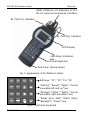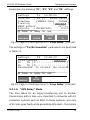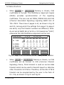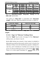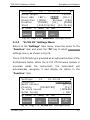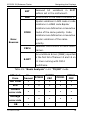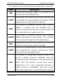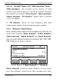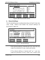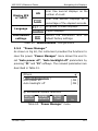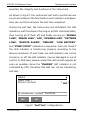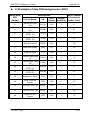
1
GAO XG2130 E1/Datacom Tester
USER’S MANUAL
XG2130 E1/Datacom Tester
Contents
Contents
Contents ...................................................................... 1
1
2
3
4
5
Overview ............................................................... 4
1.1
Icon Description .................................................. 4
1.2
Product Overview ................................................ 5
1.3
Product Compositions........................................... 8
1.4
Functional Keyboard ............................................ 9
1.5
LED Indicators ...................................................12
1.6
LCD icon indications............................................16
Getting Started .................................................... 19
2.1
Unpacking Check................................................19
2.2
Power Supply.....................................................21
2.3
Switch-On.........................................................24
2.4
Communication with PC.......................................26
Navigating the Displays ....................................... 28
3.1
Menu Overview ..................................................28
3.2
“Settings” Menu .................................................30
3.3
“Results” Menu ..................................................75
3.4
“Storages” Menu .............................................. 107
3.5
“Others” Menu ................................................. 113
Performing Measurements ................................. 122
4.1
Overview ........................................................ 122
4.2
Perform the Measurements ................................ 123
Technical Specifications ..................................... 157
5.1. “E1” Specifications............................................ 157
5.2. “G.703 CO” Specifications .................................. 160
5.3. “Datacom” Specifications ................................... 161
72-0027-03A
1
XG2130 E1/Datacom Tester
Contents
5.4. “Protocol Converter” Specifications ......................168
5.5. Other Specifications ..........................................168
6
Working with TestManager ................................. 169
6.1. Software Functions............................................169
6.2. System Configuration and Running Environment ....170
6.3. Install and Uninstall the Software on the PC ..........170
6.4. How to Use TestManager Software .......................171
7
Troubleshooting ................................................. 174
Appendix A: E1 Frame Structure............................... 176
1.
PCM30/PCM31 Frame Format ..............................176
2.
PCM30CRC/PCM31CRC Frame Format...................178
Appendix B: Datacom Adapter Cables ....................... 180
1.
V.24 Adapter Cable PIN Assignments (DTE) ...........180
2.
V.24 Adapter Cable PIN Assignments (DCE)...........181
3.
V.35 Adapter Cable PIN Assignments (DTE) ...........182
4.
V.35 Adapter Cable PIN Assignments (DCE)...........183
5.
V.36 Adapter Cable PIN Assignments (DTE) ...........184
6.
V.36 Adapter Cable PIN Assignments (DCE)...........185
7.
RS-449 Adapter Cable PIN Assignments (DTE).......186
8.
RS-449 Adapter Cable PIN Assignments (DCE).......187
9.
X.21 Adapter Cable PIN Assignments (DTE)...........188
10.
X.21 Adapter Cable PIN Assignment (DCE)............189
11.
RS-485 Adapter Cable PIN Assignments (DTE).......190
12.
RS-485 Adapter Cable PIN Assignments (DCE).......191
13.
EIA-530 Adapter Cable PIN Assignments (DTE) ......192
14.
EIA-530 Adapter Cable PIN Assignments (DCE)......193
15.
EIA-530A Adapter Cable PIN Assignments (DTE) ....194
72-0027-03A
2
XG2130 E1/Datacom Tester
16.
Contents
EIA-530A Adapter Cable PIN Assignments (DCE) ... 195
Appendix C: G.703 CO Adapter Cable ....................... 196
Appendix D: Special Adapter Cables......................... 197
Appendix E: Abbreviation ........................................ 198
72-0027-03A
3
XG2130 E1/Datacom Tester
1
Overview
Overview
This chapter briefly describes the relevant icons, E1/Datacom
tester overview, product compositions, functional keyboard, LED
alarm and status indications and LCD icon indications in this
operation manual.
1.1. Relevant icon information
1.2. Product overview
1.3. Product compositions
1.4. Functional keyboard
1.5. LED indicators
1.6. LCD icon indications
1.1
Icon Description
Some important information and items requiring special
attention in this manual are described with following icons.
“Note” symbol: indicates some details that should be
dealt with special caution when operating the
instrument and reminds user’s attention.
“Info” symbol: indicates some relevant information
that user still need be told to know about after
finishing some operating descriptions.
“Warning” symbol: indicates that user should refer to
the manual instruction in order to protect the
apparatus against damage.
The information after these icons in the operation manual must
be noted to ensure the right and safe operation of this
72-0027-03A
4
XG2130 E1/Datacom Tester
Overview
instrument.
1.2
Product Overview
This E1/datacom tester is one multi-functional and full- featured
digital transmission system test device, designed for the
installation,
engineering
check
and
acceptance,
daily
maintenance of the digital networks, mainly performing bit error
test, alarm analysis, fault finding and signaling analysis. In
addition, the E1/Datacom tester further provides various
commonly used protocol converters with one-directional and
bi-directional bit error test function. This instrument mainly has
following functions:
u
E1 Testing:
•
75Ω (Unbalanced) and 120Ω (Balanced) line interfaces
•
HDB3 and AMI line codes
•
Out-of-Service framed and unframed testing
ü
2Mb/s, N×64Kb/s BER testing
ü
Frame data and alarm monitoring
Frame data: FAS/NFAS, TS16 and timeslot data
Alarm: Signal Loss, AIS, Frame Loss, Remote Alarm,
Mframe alarm, Pattern Loss and BIT, CODE, FAS, E-BIT
errors and so on.
ü
•
Clock slip measurement
In-service framed and unframed testing
ü
Hi-Z and Through mode testing
ü
CODE, FAS, CRC4 and E-BIT BER testing
ü
Frame data and timeslot activity monitoring
72-0027-03A
5
XG2130 E1/Datacom Tester
Overview
ü
Built-in 64kb/s tone channel listen capability
ü
CAS and CCS signaling monitoring
•
Round trip delay measurement
•
APS delay measurement
•
PCM simulator
ü
Extensive alarm generation
ü
Frame data Si, Sa, A, FAS, CRC-4, MFAS, NMFAS and EBIT control and monitoring
ü
Idle word timeslot insertion
ü
VF tone generation and measurement
ü
CAS and CCS signaling generation and monitoring
•
Frequency, offset and level measurement
•
Up to ±999ppm transmit clock deviation
•
Transmit
clock:
Internal,
Interface
and
External
2M
clock/signal (option)
•
u
•
Real time transmit circuit open/short indication
Datacom Testing:
Datacom (V.24, V.35, V.36, X.21, RS-449, RS-485, EIA-530,
EIA-530A) BER testing
•
Asynchronous BER testing with baud rate 50b/s~57.6Kb/s
•
Synchronous BER testing with data rate 1.2Kb/s~38.4Kb/s
and Nx64Kb/s(N=1~32)
•
DTE or DCE emulation mode
•
Synchronous clock source and sense selection
Clock source: Internal or Interface
Clock sense: Rising edge or falling edge
72-0027-03A
6
XG2130 E1/Datacom Tester
•
Frequency and offset measurement
•
Handshaking signals control and monitoring
u
G.703 64kb/s CO Testing:
•
G.703 CO 64kb/s BER testing
•
Octet timing control and monitoring
•
Frequency and offset measurement
•
Transmit clock: Internal or Interface
Overview
u Protocol Converter Testing:
•
E1-Datacom synchronous 64kb/s, Nx64kb/s BER testing
Datacom interface: V.24, V.35, V.36, X.21, RS-449, RS-485,
EIA-530, EIA-530A
•
E1-G.703 CO synchronous 64kb/s BER testing
•
One-directional data conversion BER testing
•
Frequency and offset measurement of receive interface
•
Handshaking signals monitoring of Datacom interface
•
E1 frame data monitoring
u Other Functions:
•
Real-time clock
•
Extensive LED/LCD alarm and status indications
•
Test pattern: PRBS, Fixed Code and 16-BIT user word
•
Error Injection: Single and Fixed Rate
•
Manual and auto-timer measurement
•
Histograms analysis of error and alarm events
•
ITU-T G.821, G.826 and M.2100 performance analysis
•
Self-test and keyboard testing
72-0027-03A
7
XG2130 E1/Datacom Tester
Overview
•
Upgradeable software via an RS232C interface
•
Up to 99 days continuance test performance
•
More than 6 hours measurement operation from a single
battery charge
•
Save/Recall of up to 10 user-defined setups and results
•
Test results could be uploaded, conserved and printed by
TestManager software
•
Built-in NiMH rechargeable can be charged with automobile
cigarette lighter battery adapter
1.3
Product Compositions
The E1/Datacom Tester is consists of following modules:
•
Hardware: Main board, Power board and Display board.
•
Software:
Embedded
software
and
surveillance
and
management PC software “TestManager”.
•
Accessories: Waterproof package, Special test cables, AC
power adapter, rechargeable batteries, automobile cigarette
lighter adapter cable and so on.
1.3.1 Appearance of the tester
•
Front panel: LCD display, LED alarm and status indicators,
keyboard.
•
Back panel: four disassembly-proof label, serial number
label.
•
Front end: E1 unbalanced signal input/output interface (L9
coaxial), DB-44 (Datacom signal input/output interface,
E1 balanced signal input/output interface, E1 external
clock/signal access interface, G.703 CO signal input/
72-0027-03A
8
XG2130 E1/Datacom Tester
Overview
output interface), 12VDC input jack.
•
Back end: end cover, slightly press the spring fins at the
two sides of end cover to remove end cover. And the user
can see battery compartment and RS232 port jack.
The appearance of the instrument is as shown in Fig 1.
1.3.2 Accessories of the tester
•
Waterproof package
•
E1 75Ω unbalanced test cable
•
E1 120Ω balanced test cable
•
G.703 CO test cable
•
Datacom interfaces adapter cables
•
Datacom interfaces loop-back adapter
•
E1 external clock/signal access cable (option)
•
AC power adapter
•
RS232 communication cable
•
Automobile cigarette lighter battery adapter cable
•
AA NiMH rechargeable batteries
•
TestManager setup CD
•
User’s manual
1.4
Functional Keyboard
The E1/Datacom tester has 16 functional keys at the front panel,
including main functional keys, softkeys, cursor keys, page keys,
a backlight key, a power switch key, a start/stop key, a single
error insert key, etc. The arrangement of functional keys and
names of keys from left to right are as shown in Fig 2. These
functional keys are described as in Table 1.
72-0027-03A
9
XG2130 E1/Datacom Tester
Overview
DB44 (Datacom, E1 balanced, G.703
CO, E1 external clock/signal interface)
E1 75Ω (Tx) Interface
E1 75Ω (Rx) Interface
LCD Display
LED Alarm Indicators
Area
Functional Keyboard
End Cover (Knock-down)
Fig 1: Appearance of E1/Datacom tester
F3
F4
Softkeys: “F1”, “F2”, “F3, “F4”
F1
F2
SETTING
RESULT
“Setting”, “Result”, “PgUp”, “Cursor
moveable left and up” key
STORAGE
OTHER
“Storage”, “Other”, “PgDn”, “Cursor
moveable right and down” key
SINGLE
START
ERR ADD
STOP
“Single Error Add”, “Start/ Stop”,
“Backlight”, “Power” key
Fig 2: Functional keyboard
72-0027-03A
10
XG2130 E1/Datacom Tester
Overview
The right key-stroke leads to one beep while wrong or
invalid key-stroke leads to two beeps. As prompt, there
will be relevant hint information in LCD display at the
same time.
Key Name
Description
Identified as “F1” to “F4”, used to select the
parameter or activity in corresponding
Softkeys
highlight place at the bottom of LCD. Each
LCD display defines one or more functions
of these softkeys.
Matched with the “Settings” menu. When
“Setting”
this key is pressed, LCD display switches to
the “Settings” menu.
Matched with the “Results” menu. When
“Result”
this key is pressed, LCD display switches to
the “Results” menu.
Matched with the “Storages” menu. When
“Storage”
this key is pressed, LCD display switches to
the “Storages” menu.
Matched with the “Others” menu. When
“Other”
this key is pressed, LCD display switches to
the “Others” menu.
When the tester is set as single error
“Single Error
insertion mode, every time this key is
Add”
pressed, one error of the set type will be
inserted in the transmit direction.
72-0027-03A
11
XG2130 E1/Datacom Tester
Overview
Manually control the start or stop activity of
“Start/Stop”
the test. Press it to start the test and press
it again to stop the test.
When page number appears in the display
“Page Up”
menu (Like “P1”, indicates that display
menu has more pages in all and is on page 1
currently), press this key to go page up.
When page number appears in the display
“Page Down”
menu (Like “P1”, indicates that display
menu has more pages in all and is on page 1
currently), press this key to go page down.
“Cursor
Moveable Left
and Up”
“Cursor
Moveable
Right and
Down”
“Backlight”
“Power”
Move the cursor upward and leftward and
the cursor can reach the position with “[ ]”.
Move the cursor downward and rightward
and the cursor can reach the position with “[
]”.
Turn on or off the LCD backlight according to
the light condition.
Switch on or off the tester.
Table 1: Functional keys descriptions
1.5
LED Indicators
The E1/Datacom tester has 12 status and alarm LED indicators
in all, including 2 status indicators and 10 alarm indicators,
mainly indicating the current operating status of instrument and
72-0027-03A
12
XG2130 E1/Datacom Tester
Overview
if any alarm is detected during the test process. The arrangement of the status and alarm LED indicators is as shown in Fig 3.
SIGNAL LOSS
FRAME LOSS
AIS
MFRAME LOSS
PATTERN LOSS
REMOTE ALARM
ERRORS
LOW BATTERY
CLOCK SLIP
CHARGE
OCTET LOSS
START/STOP
Fig 3: LED Indicators
Status and alarm LED indicators are described as in Table 2.
LED Name
START/
STOP
Description
As “Start/Stop” key keeps changing status, this
indicator turns on (green) when the test is started
and turns off when the test is stopped.
The tester has built-in rechargeable batteries and
CHARGE
a rapid-charging circuit. This indicator turns on
(orange) when the tester is under charging and
turns off when it is fully charged.
Effectively indicates a loss of signal. When the
receiver detects 255 consecutive 0s, an alarm is
SIGNAL
generated and this indicator turns on (red). Alarm
LOSS
cleans on detecting at least 32 1s in consecutive
255 bits and LED turns off. (Comply with ITU-T
G.775 / G.962)
72-0027-03A
13
XG2130 E1/Datacom Tester
Overview
Alarm happens on receiving less than 3 0s in 512
AIS
bits and cleans on detecting more than 2 0s in
512 bits and the LED will be turned off. (Comply
with ITU-T O.162)
Alarm
happens
on
receiving
3
or
more
FRAME
consecutive FAS words in error and LED turns on
LOSS
(red). Otherwise the alarm is cleaned and LED
turns off. (Comply with ITU-T G.706)
Alarm happens on synchronization loss of CAS or
CRC4 Multiframe and the LED turns on (red).
Alarm cleans on both of these two alarms
recovering and the LED turns off.
MFRAME
LOSS
CAS Multiframe Loss: Alarm on receiving 2
consecutive MFAS words in error and the LED
turns on. Otherwise the alarm is cleaned.
CRC4 Multiframe Loss: Alarm on receiving 915 or
more CRC4 code words out of 1000 received in
error and LED turns on. Alarm cleans on receiving
2 valid MF alignment words in 8ms.
Alarm happens on receiving 6 or more bits in
PATTERN
error in consecutive 64 bits and the LED turns on
LOSS
(red). Otherwise the alarm is cleaned and the LED
turns off.
Alarm happens on detecting at least 1 error and
ERRORS
the LED turns on (red). The error sources: BIT,
FAS, CODE, CRC4 and E-BIT.
72-0027-03A
14
XG2130 E1/Datacom Tester
Overview
Alarm happens on detecting Remote Alarm or
Remote Multiframe Alarm and the LED turns on
(red). Alarm cleans on both of two disappear and
the LED turns off.
Remote Alarm: Alarm happens on receiving 1 at
REMOTE
ALARM
Bit3 in 3 consecutive NFAS words and the LED
turns on (red). Alarm cleans on receiving 0 at Bit3
in 3 consecutive NFAS words. (Comply with ITU-T
O.162)
Remote Multiframe Alarm: Alarm happens on
receiving 1 at Bit6 of timeslot 16 in frame zero in
consecutive multiframes and the LED turn on.
Otherwise the alarm is cleaned.
Alarm happens on when one or bits have been
CLOCK
SLIP
added to or deleted from a received PRBS
pattern,
and
the
LED
turns
on
(red).
In
out-of-service testing, when the test pattern is
PRBS, a clock slip will be counted in seconds.
Alarm happens on not receiving octet timing
OCTET
LOSS
violations for 8 consecutive octets in G.703 CO
testing and the LED turns on (red). Alarm cleans
on the receipt of the first octet violation and the
LED turns off. Only valid for G.703 CO testing.
LOW
BATTERY
72-0027-03A
Alarms happens on the built-in NiMH battery’s
voltage has dropped to a low level without
external power supply. And the LED turns on (red)
15
XG2130 E1/Datacom Tester
Overview
to prompt the user that an external power is
needed. In case the instrument is powered by
external power, the LED turns off soon.
Table 2: Descriptions of status and alarm indicators
1.6
LCD icon indications
The E1/Datacom tester has 5 LCD icons which are displayed at
the upper right corner of the LCD and with different indications
respectively. Various LCD icons are described in Table 3.
Icon type
Historical
Errors or
Alarms
Descriptions
When there have been historical errors or
T
alarms happened during the elapsed time
of one test, the icon flashes once every
other second to prompt the user.
Icon flashes on detecting open status of
E1 transmit circuit. Real time indicates to
B
E1
Transmit
Circuit
Status
prompt the user the transmitter is not
connected with the cable or the cable is
open circuit or broken. This icon can be
used to judge if the cable is properly
connected or damaged.
Icon flashes on detecting short status of
E1 transmit circuit. Real time indicates to
prompt the user the cable is in short
status. This icon can be used to judge if
the
cable
is
properly
connected
or
damaged.
72-0027-03A
16
XG2130 E1/Datacom Tester
Overview
Icon flashes on that the automatic test
timer has been set and indicates the
Timer
Testing
Mode
½
tester
will
start
the
automatic
test
function at the specified time. This icon
displays in real time to prompt the user
that the pre-determined timer has been
set.
Icon flashes on that the configuration
items in the “Settings” menu have been
locked, or the storage capacity is full, or
stored settings and results have been
locked, to prompt the user that one test
has been started and configuration items
Ï can not be modified any more, or the
storage capacity is full, existing records
Status
Lock
have to be deleted firstly to save the new
records, or that stored record has been
locked and has to be unlocked firstly
before it can be overwritten.
Icon flashes on that the configuration
items can be modified, the storage
capacity is not full, stored records have
Ð been unlocked, to prompt the user that no
test
is
running
yet
and
all
the
configuration items can be modified; or
storage capacity is not full and new
72-0027-03A
17
XG2130 E1/Datacom Tester
Overview
records can be saved, or that stored
record is under the unlocked status and
can be deleted.
Icon flashes on that no valid 2 MHz clock
or 2 Mb/s signal is presented at E1
external clock receiver when selecting E1
Clock Loss
transmit clock source as “External”, or no
valid clock signal is detected at the
datacom receiver by the instrument when
performing
measurements
with
the
datacom interfaces.
Table 3: Descriptions of LCD icon indications
72-0027-03A
18
XG2130 E1/Datacom Tester
2
Getting Started
Getting Started
This chapter briefly introduces the unpacking check, power
supply, switching on, communication with PC and other attention
points of the instrument.
2.1. Unpacking check
2.2. Power supply
2.3. Switch-on
2.4. Communication with PC
2.1 Unpacking Check
In order to safely transport, the E1/Datacom tester is packed
with carton, and with all accessories,in a waterproof package.
Be sure not to connect this instrument to any signal
cable carrying hazardous voltage!
Please check when receiving the product:
•
If the packing carton is impaired and if the appearance of the
product is impaired;
•
If the product and all its accessories are available.
•
The product with the standard configurations is consists of
following items, as shown in Table 4 :
Optional Configuration:
If the E1 External Clock/Signal optional function is ordered,
the hardware, software and
72-0027-03A
its accessory (E1 External
19
XG2130 E1/Datacom Tester
Getting Started
Clock/Signal Access Cable) will be provided.
Item
E1/Datacom Tester
75Ω Unbalanced Test
Cable
Qua
1
2
Item
Qua
Embedded Software
1
TestManager Setup CD
1
AC Power Adapter
1
120Ω Balanced Test Cable
1
User’s Manual
1
Datacom Adapter Cables
4
Waterproof Package
1
G.703 CO Test Cable
1
Maintenance Card
1
Datacom Interfaces
Loop-back Adapter
RS232 Communication
Cable
1
1
Automobile Cigarette
Lighter Battery Adapter
1
Cable
Quality Certificate
Card
Packing list
AA NiMH Rechargeable
Batteries (Built-in)
1
1
5
Table 4: Standard configurations of the E1/Datacom tester
Please check the product item by item according to the
packing list. Please contact the supplier if anything is
missing.
If necessary, keep the packaging materials in case they
will be needed some time.
72-0027-03A
20
XG2130 E1/Datacom Tester
Getting Started
2.2 Power Supply
This instrument can be powered by external power supply or
rechargeable batteries.
2.2.1
External Power Supply
The external power supply requires a power source of 110V to
240V AC at a frequency between 50Hz to 60Hz (nominal).
And the tester requires a nominal DC supply of 12V. Plug the
AC power cord into an appropriate AC wall outlet and connect
the instrument with adapter cable. And the instrument can be
powered by external power supply via the AC adapter.
2.2.2
Rechargeable Batteries
The rechargeable batteries will typically power the instrument
for more than 6 hours with the backlight off and Bit Error
measurement
selected.
The
instrument
uses
5
high-performance 1800mAH Nickel Metal Hydride (NiMH)
rechargeable batteries placed in the battery compartment that
may not be fully charged when the user receive the instrument.
Whatever the state of charge, use the instrument the battery
is completely exhausted before giving it its first charge. This
will ensure better accuracy from the battery charge indicator.
Do not change battery model!
Do not use old and new rechargeable batteries together!
Do not use non-rechargeable battery, in case that may
be cause the battery explosion or other danger!
72-0027-03A
21
XG2130 E1/Datacom Tester
Getting Started
Replacement of Rechargeable battery
A new rechargeable battery can be charged and discharged for
about 800~1000 times before it can not be used any more.
Normally the fully charged batteries could support the
instrument continuous 6 hours working depending upon the
test settings. So when the operating duration of the battery is
apparently reduced, the batteries should be replaced.
We suggest that the rechargeable batteries should be
replaced every one or two years!
Method of Battery Replacement:
Ensure the instrument is switched off firstly. And open the end
cover of the instrument and slightly press the battery
compartment lock card downward, the battery case will pop
out. Extract the battery compartment and unscrew the screws
on the top of the case to open and replace new batteries (Be
careful of not mistaking the polarity of the battery). When the
battery compartment has been loaded again, slip it back into
the battery case frame and push the battery compartment
inside (Put your fingers upon the case rather than the battery
case lock card), the battery case is installed well while a “click”
sound is heard. The battery replacement is completed when
the end cover of the instrument is mounted again.
When the batteries supplied for this instrument have
been expired the charging life or are impaired, they
72-0027-03A
22
XG2130 E1/Datacom Tester
Getting Started
should be dealt with control. If dealt with general waste
processing system or detained in the instrument, they
will harm the environment. The waste batteries should
be recycled or disposed of properly at special recycling
station or hazardous waste collection center.
2.2.3
Charging the Battery
To recharge the battery, plug in the charger using an
appropriate adapter (supplied). Normally the battery will be
fully charged after 2.5 hours. In exceptional circumstances
where the battery may have become deeply discharged, a
charge time of 24 hours may be required. Note that the
instrument can be used while the battery is charging. During
rapid charging, the “Charge” indicator turns on. When the
rapid charging is completed, charging automatically turns into
a trickle charge, the “Charge” indicator turns off. The
instrument certainly can be recharged when it is powered off,
the charging indicator can give the right display.
In addition, the battery can be recharged with automobile
charger, at this time an automobile cigarette lighter adapter
cable is needed.
2.2.4
“Low Battery” Indication
When being powered by the battery, this instrument can give
the early alarm to low battery voltage and the “Low Battery”
indicator turns on. After being used for a couple of hours, the
battery voltage continues to drop to a low level, and the
instrument will automatically perform protective shutdown.
72-0027-03A
23
XG2130 E1/Datacom Tester
Getting Started
When the “Low Battery” indicator turns on, the external
power supply is needed to support the instrument working
while the battery is charging.
2.2.5
Power Management
This instrument provides automatic power-off function. When
the instrument is not under test-started status and there is no
keystroke in 5 minutes, this instrument will be turned off
automatically. This function can effectively prevent the
instrument from being accidentally turned on and the battery
from being exhausted during transport. This function can be
set to ON or OFF in “Others” menu.
The LCD backlight can be turned on by pressing the
“Backlight” key, and be automatically turned off in 30
seconds. This function can be set to ON or OFF in “Others”
menu. When set as OFF, press the “Backlight” key to turn on
the backlight, and press the “Backlight” key again to turn off
the backlight.
2.3 Switch-On
2.3.1
•
Switch-on Inspection Steps
Plug in AC adapter with power cord, the “Charge”
indicator of this instrument will turn on;
•
This instrument can be switched on after “Power” key has
been pressed for about 1 second, LCD displays company’s
LOGO and the software version information embedded in
the instrument. About 1 second later, the switch-on
process is completed and LCD display the setting’s menu
72-0027-03A
24
XG2130 E1/Datacom Tester
Getting Started
after one beep.
•
This instrument can be switched off by pressing the
“Power” key again for 1 second. When the battery has
been fully recharged, remove the AC power adapter. After
powering of battery, this instrument can be switched on or
off by pressing the “Power” key.
•
Loopback the 2Mb/s input and output interface of the
instrument with E1 75Ω unbalanced test cable.
•
Switch on the instrument and check if LCD displays and
LED indicators are abnormal.
•
Select error insertion type as “BIT”, “Single”, and press
the “Single Err Add” key to check if the instrument
detects and operates properly.
•
When the user receives the instrument at the first time,
please use the instrument until the battery is completely
exhausted before giving it its first charge.
2.3.2
Setting the Time and Date
At the top line of the screen, LCD displays the current time, in
the format of “Hour: Minute: Second”, with 24-hour system.
Because the test result is time-stamped, therefore it is
necessary to set right time and date before using this
instrument.
Time and date can be set in the real-time clock settings in the
“Others” menu, by following operational steps:
•
Press the “Other” key to switch to the “Others” menu,
select TIME&DATE by the softkeys.
72-0027-03A
25
XG2130 E1/Datacom Tester
•
Getting Started
Select SETUP to “Clock Mode” item, and then the date
and time of the instrument can be modified.
•
Choose the RUN status after date or time has been set,
and then the instrument can work according to the newly
setting time.
2.3.3
Self-test
Before making measurements, run a self-test to check that the
instrument is operating correctly. The user may find self-test
function in the “Others” menu. Please refer to the “Others”
menu descriptions for details.
2.4 Communication with PC
This instrument supports communication with PC via RS232C
interface by TestManager software. And TestManager can do two
jobs: one is to upload the test results stored in the instrument to
PC for further processing including filing, printing and analyzing,
and the other is to upgrade the embedded software via PC to
protect your investment.
2.4.1
Communication Steps
•
Switch off the instrument firstly.
•
Open the end cover of the instrument.
•
Connect RS232 interface of the instrument to PC serial
port with RS232 communication cable (supplied).
•
Switch on the instrument.
•
Set RS232 port state to ON in “Others” menu.
•
Run the TestManager software on PC, click “Select” to
choose the type and click “Connect” icon. After the
72-0027-03A
26
XG2130 E1/Datacom Tester
Getting Started
successful connection the user can upload, view, analyze,
delete, print test results in the form of report and do other
operations.
Be sure not to plug and unplug the communication cable
alive when connecting PC serial interface to the
instrument using the serial communication cable, and be
sure to ground or use ESD wrist strip. During serial data
communication period, the instrument can be powered
either by built-in batteries or by AC power adapter.
2.4.2
Upgrading the Embedded Software
We will launch the latest version embedded software and host
software TestManager in the website of our company for the
users to download. Make sure to visit our website frequently to
ensure you will always get the software of the latest version.
For the software upgrading method, please refer to the
relevant part of “Communication with PC” and follow
instruction of the TestManager.
When performing the embedded software upgrading, in
order to prevent the instrument powered off caused by
the battery exhausted, it is strongly recommended to
use external AC power supply to power the instrument.
72-0027-03A
27
XG2130 E1/Datacom Tester
3
Navigating the Displays
Navigating the Displays
This chapter first briefly gives an overview of the four main
operation menus, and then explains the relevant operations of
these four main operation menus in details.
3.1
3.1
Menu overview
3.2
“Settings” menu
3.3
“Results” menu
3.4
“Storages” menu
3.5
“Others” menu
Menu Overview
The operation menus of the E1/Datacom tester includes
“Settings”, “Results”, “Storages”
and “Others”
menu,
matched with the “Setting”, “Result”, “Storage” and “Other”
keys respectively. These four menus can be switched from one
another at any time by pressing these four keys. “PgUp” and
“PgDn” keys provide page up and down functions, “Cursor
Right and Down” and “Cursor left and Up” keys provide
cursor movement functions, “F1”, “F2”, “F3”, “F4” softkeys are
used to select the parameter or actions at the bottom of LCD
which matched with the place highlighted by the cursor.
In each of display areas the field currently able to be changed is
marked by a “Highlighted cursor”. The menu of selection
available for the active field is displayed on softkeys on the
bottom of the display. The choice from the menu is made using
the keys situated immediately below the display. The highlighted
72-0027-03A
28
XG2130 E1/Datacom Tester
Navigating the Displays
cursor is moved around the display using page and cursor keys.
When a highlighted field has more than 5 choices a softkey
labeled >> is provided. When >> is chosen the remainder of the
menu is revealed.
“Settings” menu
Press the “Setting” key to enter into the settings menu. Press
the “Cursor Right and Down” and “Cursor left and Up” keys
to move the cursor, press the “F1”, “F2”, “F3” and “F4” softkeys
to select the corresponding parameters. In case page number
appears in the menu, turn page by pressing the “PgUp” or
“PgDn” key. Press the “Start/Stop” key to start the test after
all the settings have already been configured completely.
“Results” menu
Press the “Result” key to switch to the result menu. “F1”, “F2”,
“F3”, “F4” softkeys are used to select various types of result
analysis and statistics. In case page number appears in the
menu, then page can be turned by pressing the “PgUp” or
“PgDn” key.
“Storages” menu
Press the “Storage” key to switch to the storage menu. Press
the “Cursor Right and Down” and “Cursor left and Up” keys
to select storage name, press the “F1”, “F2”, “F3”, “F4” softkeys
to view, delete, lock, unlock, rename and other actions to the
settings and results of the record. In the stored results, the
72-0027-03A
29
XG2130 E1/Datacom Tester
Navigating the Displays
instrument setting and result information of any test result are
available.
“Others” menu
Press the “Other” key to switch to the auxiliary information
menus. Following auxiliary information menus can be accessed
by pressing the “F1”, “F2”, “F3” and “F4” softkeys, including
miscellaneous, power manager, time & date, RS232 port,
keyboard
test,
self-test,
tester
information,
producer
information and so on.
Status prompt information line provides operating status
of the instrument.
The upper right corner of LCD “Ð ” indicates that the
parameters can be modified, “Ï” indicates that the
instrument is doing one test, softkeys are under the lock
status, and configuration data can not be modified. “Ð ”
in the storage menu indicates that there still has storage
space to save more records in the instrument, “Ï”
indicates that no saving space is available, some records
must be deleted first to save the new records. “Ð ” and
“Ï” following each saved record respectively indicate
that the record is under locked or unlocked status.
3.2
“Settings” Menu
“Settings” menu mainly performs the selection of the test
function and the settings of relevant parameters, which are
associated with the situation of the system under test. Only after
72-0027-03A
30
XG2130 E1/Datacom Tester
Navigating the Displays
setting relevant parameters and performing the correct test
connections can be the test process accomplished properly.
Every time the instrument is switched on again, the instrument
automatically uses the settings menu of the last valid test as the
default setting menu. Only the start-stop processing test can
become one valid test.
Press the “Setting” key to switch to the “Settings” menu, the
user can select E1, DATACOM, PROTOCOL CONVERTER,
G.703 CO to set test functions. The parameters of settings may
vary from function to function. And below will explain the
settings respectively.
E1/Datacom tester, in case the instrument does not carry the
G.703 CO module, its option will not show up in the “Function”
option. And the user can not make the relevant measurements.
3.2.1
“E1” Settings Menu
3.2.1.1
“TX/RX” Mode
“TX/RX” mode mainly performs out-of-service framed or
unframed bit error test to E1 transmission networks. The
display is shown as Fig 4. The settings may be changed by
framing format selection. The settings of relevant framing are
described in Table 5. The settings of relevant PCM30,
PCM30CRC, PCM31 and PCM31CRC are shown in Appendix A:
“E1 Frame Structure”.
a. “TX/RX” Mode Unframed Settings
An unframed test pattern which internally generated is
72-0027-03A
31
XG2130 E1/Datacom Tester
Navigating the Displays
transmitted by the transmitter of the instrument and is sent
into the network under test. And this test pattern will be
looped back to the receiver. The instrument makes bit error
test and analysis based on the comparison of the transmitted
and received data.
Settings
P1
10:30:00
Ð
Fu nc t io n
[ E1 ] [
T X /R X ]
In terface
[UNBAL 75Ω]
[HDB3 ]
Framing
[PC M30 ]
BERT pattern
[2 1 5 -1]
Po l a r it y
[ I N V E RT E D ]
I T U -T
i Tester is ready for use
DATACOM
E1
PROTOC
CONVER
G.703
CO
Fig 4: Page 1 of “Settings” menu
Framing
UNFRAMED
The “unframed” data is a 2.048Mb/s serial
binary data stream without framing.
Framed E1 with Channel Associated Signaling
PCM30
(CAS) multiframe.
PCM30CRC
PCM31CRC
PCM31
Description
Framed E1 with Channel Associated Signaling
(CAS) and CRC4 multiframe.
Framed E1 with CRC4 multiframe.
Framed E1 with no multiframe.
Table 5: “Framing” parameter settings
•
Page 1 of “Settings” menu in “TX/RX” mode (unframed)
72-0027-03A
32
XG2130 E1/Datacom Tester
Navigating the Displays
TX/RX unframed testing mode has 2 pages, with the page 1
as shown in Fig 5.
Settings
P1
10:30:00
Ð
Function [ E1 ] [
TX/RX ]
Interface
[UNBAL 75Ω]
[HDB3]
Framing
[UNFRAMED]
BERT pattern
[2 1 5 -1]
Po l a r it y
[ I N VE RT ED ]
I T U -T
i Tester is ready for use
TX/RX
RX HI-Z
THROUGH
>>
Fig 5: Page 1 of “Settings” menu in “TX/RX” (Unframed)
Under UNFRAMED mode, in page 1 of the settings menu,
move the cursor to the parameter’s positions corresponding to
“Interface”, “Framing”, “BERT pattern”, “Polarity”, and
select relevant parameters by pressing “F1”, “F2”, “F3”, “F4”
softkeys.
The setting parameters of “Interface” are described in Table 6.
The settings parameters of “Framing” are described in Table 5.
The setting parameters of “BERT pattern” and “Polarity” are
described in Table 7.
Item
Interface
72-0027-03A
Option
UNBAL
75Ω
Descriptions
The line impedance is unbalanced 75Ω,
connected
with
coaxial
cable.
The
physical connector is L9.
33
XG2130 E1/Datacom Tester
Navigating the Displays
The line impedance is balanced 120Ω,
BAL
120Ω
connected with twisted pair wires, the
red cable transmits and the yellow cable
receives
the
signals.
The
physical
connector is crocodile clamp.
The line code is a High Density Bipolar 3
which is one of the commonly used line
code to perform the base-band signal
transmission in the digital networks.
HDB3
HDB3 coding was adopted to eliminate
the synchronization problems occurring
with AMI. In HDB3 format, a string of
four consecutive zeros is replaced with a
substitute
string
containing
an
intentional BPV (Bi-Polar Violation).
Line
The line code is an Alternate Mask
Code
Inversion.
AMI
coding
is
used
to
represent successive 1s in a bit stream
with alternating positive and negative
pulses. A zero bit will not generate any
AMI
pulse. AMI coding is not used in most E1
transmissions
because
of
synchroni-
zation loss during long strings of data
zeros. (Note: “Signal loss” alarm will be
generated when transmitting unframed
all “0” in AMI code.)
Table 6: “Line Interface” parameter settings
72-0027-03A
34
XG2130 E1/Datacom Tester
Item
Navigating the Displays
Option
223-1
211-1
Descriptions
215-1 Pseudorandom Binary Sequence
(PRBS) is suitable for bit error rate
9
2 -1 measurement.
BERT
1111
pattern
0000
1010
16BIT
Fixed code or static binary code
can simulate AIS (1111) and etc.
16-BIT is a user programmable
word.
The
instrument
transmits
and
receives PRBS code according to
NORMAL
the normal “1” or “0” polarity. Code
“1” is transmitted as “1”, and code
“0” is transmitted as “0”.
Polarity
The
instrument
transmits
and
receives PRBS code according to
INVERTED
the reverse polarity. Code “1” is
transmitted as “0”, and code “0” is
transmitted as “1”.
Table 7: “Test Pattern” and “Polarity” parameter settings
Note, when performing measurements between two testers
and the test pattern polarity transmitted is not confirmed, the
user could switch to the reverse pattern.
•
Page 2 of “Setting” menu in “TX/RX” mode (unframed)
Press the “PgDn” key to enter into the page 2, as shown in Fig
72-0027-03A
35
XG2130 E1/Datacom Tester
Navigating the Displays
6. Press the “Cursor Right and Down” key to move the
cursor to the positions to set “Transmit clock”, “Error add”,
“Resolution”, “Storage” and “Duration” parameters, and
select relevant parameters by pressing “F1”, “F2”, “F3”, “F4”
softkeys.
The setting parameters of “Transmit clock” are described in
Table 8. The setting parameters of “Error add” are described
in Table 9a and Table 9b. The setting parameters of
“Resolution”, “Storage” and “Duration” are described in
Table 10.
Settings
P2
10:30:00
¾Ð
Tx clk [INTERN ]
2048K [+10ppm]
Error add
[BIT]
[RATE]
[ 1E-2]
Re so l ut i on [ 1 M I N ]
Storage [ NO]
Duration
[TIMER]
[ 01] [MIN]
Start
[2004 /04/26]
[10 :25 :36 ]
i
Tester is ready for use
INTERN
RX CLK
Fig 6: Page 2 of “Settings” menu in “TX/RX” (Unframed)
Item
Option
Tx clk
INTERN
Descriptions
Default.
The
transmit
clock
sourced from the internal crystal.
The transmit clock is derived
RX CLK
from the received signals at the
receiver.
72-0027-03A
36
XG2130 E1/Datacom Tester
Navigating the Displays
Optional. The transmit clock is
derived from the external 2.048M
Hz clock signal which complied
EXTERN
2Mb/s clock
(Option)
with TTL standard electrically,
i.e., the 2MHz square wave signal
input,
as
source,
the
the
transmit
yellow
clock
cable
is
connected to the clock signal and
the black cable is connected to
signal ground.
Optional. The transmit clock is
EXTERN
derived
from
2Mb/s
standard
2Mb/s
signal
which
accessed
(Option)
is
the
external
HDB3
signal
with
75Ω
coaxial L9 connector through the
special access cable.
The
+10
Frequency
PPM
+1
internal
clock
can
be
deviated in the range of ±999ppm
PPM with the step length of 1 ppm.
One application of this function is
deviation
-10
-1
PPM
PPM
to
test
the
clock
recovering
capability in receive circuit of the
multiplexer under test.
Table 8: “Transmit clock” parameter settings
72-0027-03A
37
XG2130 E1/Datacom Tester
Item
Option
BIT
FAS
Error
add
type
Navigating the Displays
CODE
CRC4
Description
Insert bit errors. (Effective under various of
unframed and framed testing)
Insert Frame Alignment Signal (FAS) errors.
(Effective only under the framed testing)
Insert CODE errors. (Effective only under
the AMI line code type)
Insert CRC4 errors. (Effective only under the
framed testing with CRC4 frame structure)
Insert E-BIT errors. (Effective only under
E-BIT
the
framed
testing
with
CRC4
frame
structure)
Table 9a: “Error add type” parameter settings
Item
Option
Description
Press the “Single Err Add” key on the
keyboard to inject one error per time. Every
SINGLE
time this key is pressed, one error such as
BIT, FAS, CODE, E-BIT, CRC4 is inserted by
the transmitter. “ERRORS” indicator turns
on for one time with a second update.
Error
Errors are injected at the constant fixed rate
add
RATE
such as 1E-2, 1E-3, 1E-4, 1E-5, 1E-6,
1E-7. In the mean time the “ERRORS”
indicator turns on.
OFF
Errors insertion is forbidden and pressing
the “Single Err Add” key is invalid.
Table 9b: “Error add” parameter settings
72-0027-03A
38
XG2130 E1/Datacom Tester
Item
Navigating the Displays
Option
Description
1MIN
The time resolution to record the
Resolution 15MINS
1HOUR
happening time of errors and alarm in
the stored event records for the
histogram analysis.
Save the test result. The menu to save
YES
the result will pop out when the test is
completed.
Storage
The test result is not saved directly,
NO
and the user can save it later in the
“CURRENT”
item
of
“Storages”
menu.
MANUAL
The test period is controlled by the
“Start/Stop” key.
User-defined duration. Test period is
initiated by pressing the “Start/Stop”
key and normally terminates at the
AUTO
Duration
end of the period but this can be
overridden by the “Start/Stop” key.
According to actual needs, the time
range can be set from 1 second ~ 99
days.
Run a timed test by programming both
TIMER
the start and stop time of this test.
The test will automatically start and
stop at the pre-determined time. And
72-0027-03A
39
XG2130 E1/Datacom Tester
Navigating the Displays
the test time range can also be set
from 1 second ~ 99 days, and the
start time can be set in the format of
Y/M/D and H/M/S. In case that the
pre-determined time is earlier than
the real-time clock of the instrument,
the test of pre-determined time does
not work, this can be overridden by
the “Start/Stop” key; If later than
the current time, the pre-determined
time works, user is not able to
manually start the test, but can stop
the test in advance manually.
Table 10: “Resolution”, “Storage” and “Duration” settings
b. “TX/RX” Mode Framed Settings
The framed testing is intended to perform the bit error test of
N×64kb/s (N=1~31) in E1 timeslots. This testing can make
the accurate assessment of transmission performance in the
selected one or more timeslots.
Select with the framed structure such as PCM30, PCM30CRC,
PCM31, PCM31CRC. There are 3 setting pages in “TX/RX”
mode, among which the setting contents of page 1 and page 3
are as same as ones in the unframed testing setting menus.
•
Page 1 of settings menu in “TX/RX” mode (framed):
Refer to the relevant parts in page 1 of the settings menu in
72-0027-03A
40
XG2130 E1/Datacom Tester
Navigating the Displays
“TX/RX” mode (unframed testing).
•
Page 2 of settings menu in “TX/RX” mode (framed)
Press the “PgDn” key to enter into page 2 of settings menu in
“TX/RX” mode (framed testing), move the cursor to the
positions
to
set
“Tx/Rx
timeslots”,
“Idle
pattern”
parameters, as shown in Fig 7. The relevant parameters to
select are described in Table 11.
Settings
P2
10:30:00
Ð
Tx/Rx timeslots
[ DIVERSE ]
Tx
TS [ F: : : : : : : : : : : : : : : :]
Rx
TS [ F: : : : : : : : : : : : : : : :]
Bandwidth T x 00 ∗64 K Rx 00∗6 4K
Id l e p a t t er n
[ 1 0 1 01 01 0 ]
i Tester is ready for use
DIVERSE
TX
AS RX
Fig 7: Page 2 in “TX/RX” mode (framed testing)
•
Page 3 of settings menu in “TX/RX” mode (framed
testing)
Refer to the descriptions of relevant parts in page 2 of settings
menu in “TX/RX” mode (unframed testing).
Item
Tx/Rx
timeslots
72-0027-03A
Option
Description
The selected timeslots in the transmit
DIVERSE direction are different to the ones in
the receive direction.
41
XG2130 E1/Datacom Tester
Navigating the Displays
The selected timeslots in the transmit
TX AS RX direction are same as the ones in the
receive direction.
Timeslot
SELECT
To select or de-select a timeslot. The
DE-
selected timeslot is marked with “*”
SELECT
and unselected one is marked with “.”.
status
Move leftward or rightward to the
←
→
timeslot that needs to be selected or
de-select.
Displays the bandwidth of the transmit
Bandwidth
No option
direction and the receive direction in
real time according to amount of the
timeslots selected respectively.
Except the timeslot 0 and timeslot 16
in PCM30/30CRC frame, other not
selected timeslots data will be replaced
by idle codes on a per-channel basis on
Idle
1
0
the transmit direction. This can be
effectively used to detect the busy or
pattern
idle activity of the timeslots.
Note: Be sure not to set all idle codes
as all “0” under AMI line code function.
←
→
Move leftward or rightward to the bit
that needs to be edited.
Table 11: “Tx/Rx timeslots” and “Idle pattern” settings
72-0027-03A
42
XG2130 E1/Datacom Tester
3.2.1.2
Navigating the Displays
“RX HI-Z” Mode
a. “RX HI-Z” Unframed Settings
Firstly choose the “Function” of the instrument as “RX
HI-Z” as shown in Fig 8. Press the “Cursor Right and
Down” key to select E1 framing as UNFRAMED. When user
set the timer to start the test, there will have 2 pages of
settings menu in “RX HI-Z” mode unframed testing,
otherwise there has only 1 page. Move the cursor to the
positions to set “Interface”, “Framing”, “Resolution”,
“Storage” and “Duration” parameters, and select relevant
parameters by pressing “F1”, “F2”, “F3”, “F4” softkeys.
Above relevant parameters are described in Table 5, 6, 10.
Settings
10:30:00
Ð
F unc t ion
[ E1 ] [
R X HI - Z ]
Interface
[U NBA L 7 5Ω]
[HDB3]
F ra m i n g
[UNF RAMED ]
Re sol ut ion
[ 1 MIN]
S tora ge [NO]
Duration
[MANUAL]
i Tester is ready for use
TX/RX
RX HI-Z
THROUGH
>>
Fig 8: Settings menu in “RX HI-Z” mode (Unframed)
b. “RX HI-Z” Framed Settings
•
Page 1 of settings menu in “RX HI-Z” mode (framed)
As shown in Fig 9, press the “Cursor Right and Down” key
to select E1 frame as the framed structure. There have 2
setting pages in “RX HI-Z” mode framed testing, as shown
72-0027-03A
43
XG2130 E1/Datacom Tester
Navigating the Displays
in Fig 9 and Fig 10. In page 1, move the cursor to the
positions to set “Interface”, “Framing”, “Idle pattern”
“Resolution” and “Storage”
parameters, and select
relevant parameters by pressing “F1”, “F2”, “F3”, “F4”
softkeys. Above relevant parameters are described in Table
5, 6, 10, 11.
S et t in g s
P1
10:30:00
Ð
Fu nc t io n
[ E1 ] [
R X H I-Z ]
In terface
[UNBA L 75Ω]
[HDB3 ]
F ra m ing
[PCM30]
Id le p a t t e r n
[ 1 0 1 01 0 1 0 ]
Res olu ti on
[ 1MI N]
Stora ge [NO ]
i Tester is ready for use
UNFRAME
PCM30
PCM30
CRC
>>
Fig 9: Page 1 of settings menu in “RX HI-Z” framed mode
•
Page 2 of settings menu in “RX HI-Z” mode (framed)
Press the “PgDn” key to enter into page 2 of the settings
menu in “RX HI-Z” mode framed testing, move the cursor to
the positions to set “Duration” parameter, and select
relevant parameters by pressing ”F1”, ”F2”, ”F3”, ”F4” keys,
as shown in Fig 10. And relevant parameters are described in
Table 10.
72-0027-03A
44
XG2130 E1/Datacom Tester
S e t t ing s
Duration
i
Navigating the Displays
P2
10:30:00
[ MANUAL ]
Ð
The tester is ready
MANUAL
AUTO
TIMER
Fig 10: Page 2 of settings menu in “RX HI-Z” framed mode
3.2.1.3
“Through” Mode
“Through” mode testing supports the instrument is bridged
as a “resistor” into an E1 path. In another word, E1 signal
transmits through the instrument receiver transparently and
to be relayed through the transmitter of the instruments.
In this mode the transmitter and the receiver of the instrument
must be connected into the E1 path, and the transmit clock of
the instrument is always extracted from the received E1 signal
to guarantee the synchronization of the signal. Because of the
transparent
transmission
through
the
instrument,
the
instrument will not change the data of received E1 and make
the measurements of error counting, frame data, signal and
timeslot analysis.
Go back to page 1 of “Settings” menu, select THROUGH in
“Function” item to set relevant parameters. All these
parameter configurations are same as those in “RX HI-Z”
mode.
72-0027-03A
45
XG2130 E1/Datacom Tester
3.2.1.4
Navigating the Displays
“Loop Delay” Mode
The time taken for voice or data traffic to pass through
network is very important as excessive delay adds distortion.
Speech is particularly affected by delays longer than 150ms.
“Loop delay” (Round Trip Delay) is a measurement of the
total delay on the “go” and “return” legs of a duplex path and
is typically in the order of milliseconds.
The instrument measure the time taken for a test pattern to be
transmitted over the “go” and “return” legs of a duplex path. A
test pattern is transmitted in an Nx64k b/s path or a 2Mb/s
unframed path and a timer is set running. A loopback is
manually applied to the network equipment to return the test
signal. The received pattern stops the timer and the round trip
delay is calculated in resolution of ±1µs.
Go back to page 1 of “Settings” menu, select LOOP DELAY in
“Function” item to set relevant parameters, as shown in Fig
11. Different formats of frame set will have different settings.
We will describe them below respectively.
a. “Loop Delay” Unframed Settings
As shown in Fig 11, press the “Cursor Right and Down” key,
select “Framing” as UNFRAMED mode. There has one page
of settings in this mode. And move the cursor to the positions
to set “Interface” parameter and select relevant parameters
by pressing “F1”, “F2”, “F3” and “F4” softkeys.
The settings of “Interface” and “Framing” parameters are
72-0027-03A
46
XG2130 E1/Datacom Tester
Navigating the Displays
described in Table 6 and Table 5.
Settings
10:30:00
Ð
F u n ct i o n [ E 1 ] [
L O OP D E L A Y ]
In t e rfa ce
[UNBA L 75Ω ]
[HD B 3]
F ra m i n g
[ UNF RAMED ]
B ERT pa t t e rn
<2 1 5 -1 >
Po larit y
< I N V E RT ED >
I T U -T
i Tester is ready for use
LOOP
DELAY
APS
DELAY
PCM
SIMULAT
>>
Fig 11: “Loop Delay” settings menu (Unframed)
b. “Loop Delay” Framed Settings
As shown in Fig 12, press the “Cursor Right and Down” key,
select the framing formats of PCM30, PCM30CRC, PCM31,
PCM31CRC. There have two pages of settings in this mode, as
shown in Fig 12 and Fig 13.
•
Page 1 of settings menu in “Loop delay” (Framed) mode
As shown in Fig 12, in page 1, move the cursor to the positions
to set “Interface” and “Framing”, and select relevant
parameters by pressing “F1”, “F2”, “F3” and “F4” softkeys.
The settings of “Interface” and “Framing” parameters are
described in Table 6 and Table 5.
•
Page 2 of settings menu in “Loop delay” (Framed) mode
Press the “PgDn” key to enter into page 2 of the settings menu
in “Loop delay” framed mode, as shown in Fig 13. Move the
cursor to the positions to set “Tx/Rx timeslots” and other
72-0027-03A
47
XG2130 E1/Datacom Tester
Navigating the Displays
parameters by pressing “F1”, “F2”, “F3” and “F4” softkeys.
S et t in g s
P1
10:30:00
Ð
Func tion
[ E1 ] [
L O O P D E L AY ]
Int e rfa ce
[U NB AL 7 5Ω ]
[HD B3 ]
F ra m i ng
[PCM30 ]
BE RT pa t te r n
<2 1 5 -1>
Pola rity
< I N V ERT E D >
I T U -T
i Tester is ready for use
UNFRAME
PCM30
PCM30
CRC
>>
Fig 12: Page 1 of settings menu in “Loop Delay” (Framed)
The settings of “Tx/Rx timeslots” parameters are described
in Table 11.
S et t in g s
P2
10:30:00
Ð
Tx/Rx timeslots
[ DIVERSE ]
Tx
TS [ F: : : : : : : : : : : : : : : :]
Rx
TS [ F: : : : : : : : : : : : : : : :]
Bandwidth T x 00∗64K Rx 00∗64K
i
Tester is ready for use
DIVERSE
TX
AS RX
Fig 13: Page 2 of settings menu in “Loop Delay” (Framed)
3.2.1.5
“APS Delay” Mode
The time taken for E1 signal transferring one to another
transmission path is also very important to networks with E1
protection systems such as SDH. In these systems, once any
of E1 links goes faulty while generating AIS alarm, the system
72-0027-03A
48
XG2130 E1/Datacom Tester
Navigating the Displays
will automatically switch that E1 link to the other standby one.
When the instrument received AIS alarm, a timer is started.
After the detection of recovery from AIS, the timer will be
stopped and the APS delay will be calculated in resolution of
±1µs. “APS Delay” is ideal for the assessment of the switching
performance in SDH optical transmission or other networks.
Go back to page 1 of “Settings” menu, select APS DELAY in
“Function” item to set relevant parameters. All these
parameter configurations are same as those in “Loop Delay”
mode.
3.2.1.6
“PCM Simulator” Mode
This instrument can make full simulation of PCM equipment,
and perform comprehensive
measurements to 2M b/s
interface of the equipment. In “PCM Simulator” mode, the
instrument provides transmit clock deviation, error insertion,
alarm generation, framing bits and signaling programming. It
can also support inserting idle codes and VF tone whose
frequency and level are adjustable in one or more timeslots.
Go back to page 1 of “Settings” menu, select PCM SIMULAT
in “Function” item to set relevant parameters. There are 2
pages of settings menu in this mode, as shown in Fig 14 and
Fig 15.
a. Page 1 of “PCM Simulator” Settings
As shown in Fig 14, press the “Cursor Right and Down” key
to move the cursor to the positions to set “Interface”,
72-0027-03A
49
XG2130 E1/Datacom Tester
Navigating the Displays
“Framing”, “Tx clk”, “Alarm injection” parameters, and
select relevant parameters by pressing “F1”, “F2”, “F3” and
“F4” softkeys.
S et t in g s
P1
10:30:00
Ð
Fu nc t io n [ E 1 ] [ P C M S I M U LA T OR ]
Interface
[UNBAL 75Ω]
[HDB3]
Framing
[PCM30]
T x cl k [INTE RN]
2 048K [+1 0ppm ]
A la r m in j e c t ion
[ F R AM E LOS S ]
i Tester is ready for use
LOOP
DELAY
APS
DELAY
PCM
SIMULAT
>>
Fig 14: Page 1 of “PCM Simulator” settings menu
The settings of “Interface”, “Framing” and “Tx Clk”
parameters are described in Table 6, 5, 8 respectively. Since
the framing data or framing synchronization may be destroyed
after some alarms are injected, therefore some error insertion
functions will be disabled accordingly. Error insertion type is
also related with the frame format, as shown in Table 12. The
settings of alarms insert ion parameters and insertionpermitted error types are described in Table 12.
b. Page 2 of “PCM Simulator” Settings
Press the “PgDn” key to enter into page 2 of “PCM
Simulator” settings menu, as shown in Fig 15. Move the
cursor to the positions to set “Error add”, “TX FAS/NFAS”,
“TS16”, “Signal Injection” and “Tx timeslots” parameters
by pressing “F1”, “F2”, “F3” and “F4” softkeys. The settings of
72-0027-03A
50
XG2130 E1/Datacom Tester
Navigating the Displays
relevant these parameters are describled in Table 9a and 9b.
S e t t ing s
P2
10:30:00
Ð
Error add
[ FAS ] [ RATE ] [ 1E-2 ]
Tx
FAS/NFAS [NORM]
TS16 [NORM]
S ig n a l inj e c ti on
[I D LE WO RD ]
[ 10101010 ]
Tx
TS
[ F: : : : : : : : : : : : : : : :]
i Tester is ready for use
FAS
CODE
CRC4
E-BIT
Fig 15: Page 2 of “PCM Simulator” settings menu
Option
Error
Description
inserted
The instrument transmits the wrong
FRAME
frame alignment signals to check if the
LOSS
equipment under test is able to give the
CODE
corresponding alarm.
If the equipment under test can give
AIS
AIS
alarm
when
the
instrument
None
If the equipment under test can give
CODE
transmits AIS (all 1) alarm.
REMOTE the alarm when the instrument sets
ALARM
CAS
MF LOSS
72-0027-03A
FAS
Bit3 of NFAS data in transmitted E1
CRC4
data stream.
E-BIT
If the equipment under test can give
CODE
the
alarm
when
the
instrument
transmits the wrong MFAS word. This
FAS
CRC4
51
XG2130 E1/Datacom Tester
Navigating the Displays
function is only effective in the frame
E-BIT
structure with CAS.
If the equipment under test can give
make the alarm when the instrument
CRC
transmits wrong CRC4 word in NFAS.
MF LOSS
This function is only effective in the
CODE
FAS
frame structure with CRC.
If the equipment under test can give
REMOTE the
alarm
when
the
instrument
MF
transmits wrong NMFAS word. This
ALARM
function is only effective in the frame
structure with CAS.
CODE
FAS
CRC4
E-BIT
Table 12: “Alarm Injection” parameter settings
The settings of “Tx FAS/NFAS” parameters are described in
Table 13.
Option
Description
Transmit FAS and NFAS word according to the
NORM
default settings of the instrument.
The FAS and NFAS word can be programmed by
user. An alarm may be generated if some relevant
EDIT
bits are changed. For instance, if A bit is set as “1”,
the equipment under test will generate remote
alarm.
Table 13: “Tx FAS/NFAS” parameter settings
The “Tx FAS/NFAS” parameter settings will switch to various
72-0027-03A
52
XG2130 E1/Datacom Tester
Navigating the Displays
menus according to the frame structure has benn set.
Note: you’d better not edit FAS or NFAS word when the alarm
has already been inserted, otherwise the new alarms may be
generated or existing alarm may disappear. In case of messy
situation, please select NORM to restore default settings.
•
When PCM30 or PCM31 framing is chosen, the user can
set Si bits, A bit, Sa4-Sa8 bits in FAS and NFAS frame, as
shown in Fig 16.
FA S / N FA S
FAS
Si
1
Si
NFAS
i
10 :30 :0 0
F A S
Ð
0 0 1 1 0 1 1
A
1 1 0
Sa4-Sa8
1 1 1 1 1
Tester is ready for use
0
1
Ú
RETURN
Fig 16: PCM30/31 “FAS/NFAS” edition
•
When PCM30CRC or PCM31CRC framing is chosen, a
CRC-4
Multiframe
is
formed.
CRC
MFAS
provides
synchronization of CRC4-Multiframe. The user can set Si
bit in FAS frame, A bit, Sa4-Sa8 bits and C1-C4 bits in
NFAS frame of F0~F15 sub-frames, as shown in Fig 17 and
Fig 18.
The settings of “TS16” parameters are described in Table 14.
“TS16” settings will be switched to different menus according
72-0027-03A
53
XG2130 E1/Datacom Tester
Navigating the Displays
to frame structure.
•
When PCM30 or PCM30CRC framing is chosen, CAS
multiframe is formed. The Multiframe Alignment Signal
(MFAS)
provides
synchronization
of
the
signaling
multiframe. The user can set MFAS, MNFAS bits and CAS
(Channel Associated Signaling) signaling ABCD bits of
TS1~TS31. There have 4 pages in all, as shown in Fig 19
and 20, (among which the settings from page 2 to page 4
are same, only the timeslot numbers are different). Note:
do not set all ABCD bits of all 30 or 31 timeslots as “0000”,
otherwise the CAS Multiframe alignment will be lost.
FAS/NFAS
P:1/3
10:30:00
F00 02 04 06 08 10
Si FAS
[0
0 0 0 0 0
F01 03 05 07 09 11
0
0 1 0 1 1
Si NFAS
A NFAS
[0
0 0 0 0 0
i Tester is ready for use
0
1
Ú
Ð
12 14
0 0]
13 15
[1 1]
0 0]
RETURN
Fig 17: Page 1 of PCM30CRC/31CRC “FAS/NFAS” edition
•
When PCM31 or PCM31CRC framing is chosen, no CAS
multiframe will be formed. In CCS (Common Channel
Signaling) frame, TS16 timeslot is used as normal data
timeslot which can be used to transmit speech or data like
other timeslots in E1 frame. Therefore, all the bits of TS16
timeslot can be programmed by the user in the form of
F0~F16, as shown in Fig 21 and Fig 22.
72-0027-03A
54
XG2130 E1/Datacom Tester
FAS/NFAS
Sa4 NFAS
Sa5 NFAS
Sa6 NFAS
Sa7 NFAS
i Tester
0
Navigating the Displays
P:2/3
10:30:00
F01 03 05 07 09 11
[1
1 1 1 1 1
[1
1 1 1 1 1
[1
1 1 1 1 1
[1
1 1 1 1 1
is ready for use
1
Ú
Ð
13 15
1 1]
1 1]
1 1]
1 1]
RETURN
Fig 18: Page 2 of PCM30CRC/31CRC “FAS/NFAS” edition
Option
Description
Transmit the TS16 timeslot according to the default
NORM
settings of the instrument.
Bits of TS16 timeslot can be programmed by the
user. An alarm may be generated if relevant bit is
EDIT
changed, if MFAS or MNFAS bit is changed, the
equipment under test may be lose multiframe
synchronization.
Table 14: “TS16” parameter settings
TS16 FORMAT
P:1/4
10:30:00
Ð
MFAS
[0 0 0 0]
NMFAS [1 0 1 1]
ABCD
ABCD
TS01
[1 0 1 0]
TS02 [1 0 1 0]
TS03
[1 0 1 0]
TS04 [1 0 1 0]
TS05
[1 0 1 0]
TS06 [1 0 1 0]
i Tester is ready for use
0
1
Ú
RETURN
Fig 19: Page 1 of PCM30/CRC “TS16” timeslot settings
72-0027-03A
55
XG2130 E1/Datacom Tester
Navigating the Displays
TS16 FORMAT
P:2/4
10:30:00
Ð
ABCD
ABCD
TS07
[1 0 1 0]
TS08 [1 0 1 0]
TS09
[1 0 1 0]
TS10 [1 0 1 0]
TS11
[1 0 1 0]
TS12 [1 0 1 0]
TS13
[1 0 1 0]
TS14 [1 0 1 0]
i Tester is ready for use
0
1
Ú
RETURN
Fig 20: Page 2 of PCM30/CRC “TS16” timeslot settings
TS16 FORMAT
P:1/2
10:30:00
Ð
MSB
LSB
MSB
LSB
F01[1 0 1 0 1 0 1 0] F02[1 0 1 0 1 0 1 0]
F03[1 0 1 0 1 0 1 0] F04[1 0 1 0 1 0 1 0]
F05[1 0 1 0 1 0 1 0] F06[1 0 1 0 1 0 1 0]
F07[1 0 1 0 1 0 1 0] F08[1 0 1 0 1 0 1 0]
i Tester is ready for use
0
1
Ú
RETURN
Fig 21: Page 1 of PCM31/CRC “TS16” timeslot settings
TS16 FORMAT
P:2/2
10:30:00
Ð
MSB
LSB
MSB
LSB
F09[1 0 1 0 1 0 1 0] F10[1 0 1 0 1 0 1 0]
F11[1 0 1 0 1 0 1 0] F12[1 0 1 0 1 0 1 0]
F13[1 0 1 0 1 0 1 0] F14[1 0 1 0 1 0 1 0]
F15[1 0 1 0 1 0 1 0] F16[1 0 1 0 1 0 1 0]
i Tester is ready for use
0
1
Ú
RETURN
Fig 22: Page 2 of PCM31/CRC “TS16” timeslot settings
72-0027-03A
56
XG2130 E1/Datacom Tester
Navigating the Displays
In E1 framed structure, idle word or audio signal can be
inserted into some timeslots based on needs, with the menu as
shown in Fig 23. The settings of “Signal injection”
parameters are described in Table 15.
Option
Description
IDLE
Insert 8-bit user-defined idle codes to one or more
WORD
timeslots, as shown in Fig 14.
Insert
VF
tone
signals
with
programmable
frequency and level to one or more timeslots,
AUDIO
frequency range: 200Hz~3400Hz with the step of
10Hz, level range: -60dBm~+3dBm.
Table 15: “Signal Injection” parameter settings
S e t t ing s
P2
10:30:00
Ð
Error add
[ FAS ]
[ RATE ]
[ 1E-2 ]
T x FAS /NFAS [NORM ]
TS16 [NO RM]
Signal injection
[ A UD IO]
[1020]Hz [-10] dBm
Tx
TS
[ F: : : : : : : : : : : : : : : :]
i Tester is ready for use
+10Hz
-10Hz
+50Hz
>>
Fig 23: “Audio” signal injection parameter settings menu
3.2.2
“Datacom” Settings Menu
3.2.2.1
Page 1 of “Datacom” Setting Menu
Return to the page 1 of “Settings” menu. Press the “F1” key in
the “Function” item to select DATACOM. There have 4 pages
in settings menu. Press the “Cursor Right and Down” key in
72-0027-03A
57
XG2130 E1/Datacom Tester
Navigating the Displays
page 1 to the positions of “Interface”, “Test mode”, “BERT
pattern” and “Polarity”, and then select relevant parameters
by pressing “F1”, “F2”, “F3”, “F4” softkeys, as shown in Fig 24.
S et t in g s
P1
10:30:00
Ð
Function
[ DATACOM ]
Inte rface
[ V. 3 5 ]
Tes t m ode
[DT E] [AS Y NC ]
BERT pattern
[2 1 5 -1]
Po l a r it y
[ I N VE RT E D ]
I T U -T
i Tester is ready for use
DATACOM
PROTOC
CONVER
E1
G.703
CO
Fig 24: Page 1 of “Datacom” settings menu
The settings of datacom “Interface” parameters are as shown
in Table 16.
Item
Interface
Option
V.24
V.35
V.36
X.21
RS-449
RS-485
EIA-530
EIA-530A
Table 16: Datacom “Interface” parameter settings
The settings of “Test mode” parameters are as shown in Table
17.
Item
Test
mode
Option
Emulation Mode
DTE
DCE
Data Framing
ASYNC
SYNC
Table 17: Datacom “Test mode” parameter settings
72-0027-03A
58
XG2130 E1/Datacom Tester
Navigating the Displays
Note:
When DTE emulation mode is chosen, the datacom
adapter cables provided with a DTE male connector
should be used. When in DCE emulation mode, the
cables provided with DCE female connectors should be
used.
The settings of “Test pattern” parameters are as shown in
Table 18.
Item
Option
220-1
211-1
Test
pattern
Description
215-1
29-1
26-1
PRBS (Pseudorandom Binary
Sequence)
Fixed code or static binary
1111
0000
1010 code
can
simulate
AIS
(1111) and etc.
16BIT
16-BIT is a user defined
word.
Table 18: Datacom “Test pattern” parameter settings
According to ITU-T recommendation, the test pattern of the
datacom transmission system is somewhat different from the
test pattern of E1 system. Please refer to Table 7 for
comparison.
The settings of pattern “Polarity” parameters are as shown in
Table 7.
3.2.2.2
72-0027-03A
Page 2 of Datacom Settings Menu in “ASYNC”
59
XG2130 E1/Datacom Tester
Navigating the Displays
Displays shown in subsequent pages vary from the datacom
test mode to the test mode. If the test mode in page 1 of the
settings is chosen as ASYNC, press the “PgDn“ key to enter
into page 2 of datacom settings menu, then press the “Cursor
Right and Down” key to move the cursor to positions to set
“Character length”, “Stop bits”, “Parity” and “Tx data
rate” parameters, and then select relevant parameters by
pressing “F1”, “F2”, “F3”, “F4” softkeys, as shown in Fig 25.
S et t in g s
P2
10:30:00
Ð
Character length
[8]
St a r t b i t
<1>
St op b it s
[ 1]
Pa rit y
[NO NE ]
T x d at a rate
[ 1. 2kb/s ]
i Tester is ready for use
6
5
7
8
Fig 25: Page 2 of “Datacom” settings menu in “ASYNC”
The settings of “Character length”, “Stop bits”, “Parity” and
“Tx data rate” parameters in ASYNC mode are as shown in
Table 19.
Item
Character
length
Option
5
Start bit
Stop bits
72-0027-03A
6
7
8
Fixed as “1 bit ”
1
1.5
2
60
XG2130 E1/Datacom Tester
ODD
EVEN
1
NONE
50b/s
75b/s
150b/s
300b/s
600b/s
1.2kb/s
2.4kb/s
4.8kb/s
9.6kb/s
19.2kb/s
38.4kb/s
57.6kb/s
Parity
Tx data
rate
Navigating the Displays
0
Table 19: “Character length”, “Stop bits”, “Parity” and “Tx
data rate” parameters
The setting of “Stop bits” is associated with “Character
length”, with their matching relations as shown in Table 20.
Character length
Stop bits settings
5, 6, 7, 8
1
5
1.5
6, 7, 8
2
Table 20: Relationship between “Stop bits” and “Character
length”
3.2.2.3
Page 3 of “Datacom” Settings Menu
Press the “PgDn” key to enter into page 3 of the “Datacom”
setting menu, as shown in Fig 25.
Before BER testing can proceed, it may nessary to establish a
data path by using the instrument control circuit. In Fig 25, the
statuses of data, clock and handshaking signals is displayed in
real-time, with V.35 datacom interface as an example. Among
which, the RS and DTR signal can be controlled as ON or OFF.
There is no clock signal necessary for ASYNC mode, so all
72-0027-03A
61
XG2130 E1/Datacom Tester
Navigating the Displays
clock signal statuses in figure are marked with “****”. Circuit
names will changed with different datacom interface chosen,
please refer to the datacom interface pin-assignments in
appendix B for the detailed circuit names of the data, clock and
handshaking signals.
S et t in g s
P3
10:30:00
SD
103 OK
RS
105
RD
104 NONE
CS
106
SCTE 113 ****
DTR 108
SCT
114 ****
DSR 107
SCR
115 ****
RLSD 109
i Tester is ready for use
ON
Ð
[ON]
OFF
[ON]
OFF
ON
OFF
Fig 25: Control circuits of a typical V.35 interface
3.2.2.4
Page 2 of Datacom Settings Menu in “SYNC”
When the test mode is chosen as SYNC, press the “PgDn” key
to enter into page 2 of “Datacom” settings menu, and press
the “Cursor Right and Down” key to move the cursor to
positions to set “Tx clock source”, “Rx clock source”, “Tx
output clock sense” and “Tx data rate” parameters, and
then select relevant parameters by pressing “F1”, “F2”, “F3”,
“F4” softkeys, as shown in Fig 26.
Before making sttings of synchronous clock, the user must
consider what transmit and receive clock configurations is to
be used, details are given in the relavant parts of chapter 4
“Performing the Measurements”.
72-0027-03A
62
XG2130 E1/Datacom Tester
Navigating the Displays
S e t t in g s
P2
Tx clock source
Rx clock source
Tx output clock sense
Tx da ta rate
i
10:30:00
Ð
[ INTERN ]
<RX CLK>
[ Û ]
[ Û ]
[ 1 . 2 Kb/s ]
Tester is ready for use
INTERN
RX CLK
Fig 26: Page 2 of “Datacom” setting menu in “SYNC”
Note:
When the X.21 interface is selected:
The Tx and Rx clocks are fixed at INTERNAL when the
instrument emulates a DCE or RX CLK when the
instrument emulates a DTE.
l
To Select the Transmit Clock Source
Move the cursor to “Tx clock source” to select the clock
source that clocks data out of the instrument. Choose
INTERNAL if you want the instrument to supply the clock,
or RX CLK if you want the system under test to supply the
clock. If INTERNAL is selected, then the “Tx data rate”
setting will appear on the display. And the user can select
a rate between 1200 b/s and 2.048M b/s (or up to 128
kb/s if the V.24 interface is selected). If the RX CLK is
selected, then you can choose which edge of the incoming
clock you want to clock data out on. Select Ÿ to clock on
the rising edge, or
72-0027-03A
to clock on the falling edge.
63
XG2130 E1/Datacom Tester
l
Navigating the Displays
To Supply a Clock to the System Under Test
The instrument supplies a clock which can be used to clock
data into the system under test. This clock is derived from
the selected “Tx clock source”. No clock is available from
the instrument if the X.21 interface is selected when the
instrument is emulating a DTE. Move the cursor to “Tx
output clock sense” setting to select
Ÿ and
which
makes the data clocked out coincident with the rising edge
or falling edge.
l
To Select the Receive Clock Source
Move the cursor to “Rx clock source” to select the clock
source that clocks data into the instrument. If the
instrument is configured DTE, the “Rx clock source” is
supplied from the INTERFACE only. If the instrument is
configured as DCE, select INTERNAL if you want to use
the clock supplied by the instrument to the system under
test, or RX CLK if you want the system under test to
supply the clock. For both DCE and DTE configurations
when INTERNAL or RX CLK is selected, you can choose
which clock edge you want to clock the data in on. Select Ÿ
to clock on the rising edge, or
to clock on the falling
edge.
The settings parameters of the synchrnous clock are as shown
in Table 21.
When making measurements in synchronization mode, the
clock configurations are pretty complex. When the instrument
72-0027-03A
64
XG2130 E1/Datacom Tester
Navigating the Displays
emulates a DTE or a DCE, the clock configurations should be
properly set, otherwise some alarms such as “Pattern Loss”,
“Errors” and “Clock Loss” will be generated.
Item
Emulation
Tx clock
DTE
source
DCE
Option
INTERNAL
DTE
Rx clock
source
DCE
RX CLK
RX CLK
INTERNAL
RX CLK
↑
↓
↑
↓
↑
↓
Tx output
↑
clock sense
↓
Table 21: Synchronous Clock Configurations
The settings of “Tx data rate” parameters are as shown in
Table 22.
Item
Option
Tx data
rate
64kb/s or
1.2kb/s
2.4kb/s
4.8kb/s
below
9.6kb/s
19.2kb/s
38.4kb/s
+1
-1
+10
-10
N×64kb/s
Table 22: “Tx data rate” configurations
3.2.2.5
Page 3 of Datacom Settings Menu in “SYNC”
Press the “PgDn” key to enter into page 3 of “Datacom”
settings menu. The instrument also detects the clock, data and
handshaking signals in SYNC mode, as shown in Fig 27. An
72-0027-03A
65
XG2130 E1/Datacom Tester
Navigating the Displays
effective clock is needed under synchronization mode. It is
very easy for the user to observe the statuses of these signals
to troubleshoot the problems when making the synchrounous
measurements.
S et t in g s
P3
10:30:00
SD
103 OK
RS
105
RD
104 NONE
CS
106
SCTE 113 OK
DTR 108
SCT
114 OK
DSR 107
SCR
115 OK
RLSD 109
i Tester is ready for use
ON
OFF
DATACOM
DATACOM
Ð
[ON]
OFF
[ON]
OFF
ON
Fig 27: Control circuits of V.35 in “SYNC”
The control circuits of “RS” and “DTR” can be set ON or OFF in
the displays.
3.2.2.6
Page 4 of Datacom Settings Menu
Press the “PgDn” key to enter into page 4 of the “Datacom”
settings menu, press the “Cursor Right and Down” key to
move the cursor to positions to set “Error add”, “Resolution”,
“Storage” and “Duration” parameters, and then select
relevant parameters by pressing “F1”, “F2”, “F3”, “F4” keys,
as shown in Fig 28.
“Error add”, “Resolution”, “Storage” and “Duration”
setting parameters are same with those in “E1” testing. All the
descriptions of these parameters are described in Table 9b,
Table 10 respectively.
72-0027-03A
66
XG2130 E1/Datacom Tester
Navigating the Displays
S e t t ing s
P4
10:30:00
Ð
B lock l e ng th
<1 00 0>
Error Add
<BIT>
[RATE]
[1E-2 ]
Resolut ion [1MIN]
Storage [YES]
Duration
[TIMER]
[01]
[MINS]
S ta r t
[200 4/0 4/26 ] [1 0:2 5:36 ]
i Tester is ready for use
SINGLE
RATE
OFF
Fig 28: Page 4 of “Datacom” settings menu
3.2.3
“G.703 CO” Settings Menu
Return to the “Settings” main menu, move the cursor to the
“Function” item and press the “F4” key to select G.703 CO
settings menu, as shown in Fig 29.
The G.703 CO testing is provided as an optional function of the
E1/Datacom tester. When the G.703 CO firmware module is
mounted
inside
the
instrument,
the
instrument
will
automatically recognize it and display its option in the
“Function” item.
S e t t ing s
P1
10:30:00
Ð
Function
[G.703 CO]
B ERT Pa t te r n
[ 2 1 5 - 1]
Po l a r it y
[ I N V ERT E D ]
I T U -T
Tx clock source
[INTERN]
Oc tet t iming
[ ON ]
i Tester is ready for use
DATACO
E1
PROTOC
CONVER
G.703
CO
Fig 29: Page 1 of “G.703 CO” settings menu
72-0027-03A
67
XG2130 E1/Datacom Tester
3.2.3.1
Navigating the Displays
Page 1 of “G.703 CO” Settings Menu
The “G.703 CO” settings menu consists of 2 pages, with the
page 1 as shown in Fig 29. Relevant parameters can be
chosen by pressing the “Cursor Right and Down” key to
move the cursor to positions to set “BERT pattern”,
“Polarity”, “Tx clock source” and “OCTET Timing”
parameters by pressing “F1”, “F2”, “F3”, “F4” softkeys.
“BERT pattern”, “Polarity”, and “Tx clock source” setting
parameters are same with those in “E1” testing. All the
descriptions of these parameters are described in Table 7,
Table 8 respectively.
The settings of “OCTET Timing” parameter are as shown in
Fig 23.
Item
Option
Description
When making measurements with the
OCTET
ON
Timing
G.703 CO interface, be sure to set the
OCTET Timing in ON status, so as to
recover circuit clock accurately.
OFF
In self-loop test, the OCTET Timing can
be set in OFF status.
Fig 23: “OCTET Timing” parameter settings
3.2.3.2
Page 2 of “G.703 CO” Settings Menu
Press the “PgDn” key to enter into page 2 of the “G.703 CO”
settings menu, press the “Cursor Right and Down” key to
move the cursor to positions to set “Error add”, “Resolution”,
72-0027-03A
68
XG2130 E1/Datacom Tester
Navigating the Displays
“Storage” and “Duration” parameters, and then select
relevant parameters by pressing “F1”, “F2”, “F3”, “F4” keys,
as shown in Fig 30.
S e t t ing s
P2
10:30:00
Ð
B lock l e ng th
<1 00 0>
Error Add
<BIT>
[RATE]
[1E-2 ]
Resolut ion [1MIN]
Storage [YES]
Duration
[TIMER]
[01]
[MINS]
S ta r t
[200 4/0 4/26 ] [1 0:2 5:36 ]
i Tester is ready for use
SINGLE
RATE
OFF
Fig 30: Page 2 of “G.703 CO” settings menu
“Error add”, “Resolution”, “Storage” and “Duration”
setting parameters are same with those in “E1” testing. All the
descriptions of these parameters are described in Table 9b,
Table 10 respectively.
3.2.4
“PROTOCOL CONVERTER” Settings Menu
“Protocol Converter” testing function always named with
“Mux/Demux” in other instruments, is used to make BER
testing for multiplexing or de-multiplexing. This function can
give the evaluation of Mux and Demux performance of the
system under test. Since the protocol converters such as
V.35-E1, V.24-E1 converters are commonly and largely used in
China, E1/Datacom tester provides this function for the
synchronous BER testing of different datacom interfaces with
the E1 interface.
72-0027-03A
69
XG2130 E1/Datacom Tester
3.2.4.1
Navigating the Displays
Page 1 of “Protocol Converter” Settings
Return to the “Settings” main menu, move the cursor to the
“Function” item and press the “F4” key to select PROTOCOL
CONVERTER settings menu, as shown in Fig 31.
The “Protocol Converter” settings menu consists of 5 pages,
in page 1, press the “Cursor Right and Down” key to move
the cursor to positions to set “Tx interface”, “Rx interface”,
“Framing”, “BERT pattern” and “Polarity” parameters, and
select relevant parameters by pressing “F1”, “F2”, “F3”, “F4”
softkeys, as shown in Fig 31.
S et t in g s
P1
10:30:00
Ð
Fun ct ion
[PR OT OC OL C ONVERT ER ]
T x in t e r fa c e
[
V. 3 5 ] [DT E ]
Rx in te r face
<E1 >
[UNBA L 75Ω ]
T x fra m ing
<SY NC >
15
BERT pattern
[2 -1]
[INVERTED]
i Tester is ready for use
DATACOM
E1
PROTOC
CONVER
G.703
CO
Fig 31: Page 1 of “Protocol Converter” settings menu
The settings of relevant “Tx interface” and “Rx interface”
parameters are as shown in Table 24.
Under the test mode of relevant protocol converters, the
matching relation of Tx and Rx interface types is as shown in
Table 25.
72-0027-03A
70
XG2130 E1/Datacom Tester
Navigating the Displays
Item
Tx/Rx
Option
V.24
V.35
V.36
X.21
RS-449
RS-485
EIA-530
EIA-530A
interface
E1
G.703 CO
Table 24: “Tx/Rx interface” parameter settings
Tx Interface
Rx Interface
V.24,
V.35,
V.36,
X.21,
RS-449, RS-485, EIA-530,
E1
EIA-530A
G.703 CO
V.24, V.35, V.36, X.21,
RS-449, RS-485,
E1
EIA-530, EIA-530A
G.703 CO
E1
Table 25: Matching relation of “Tx” and “Rx” interface
The test data bandwidth is determined by the Tx interface
settings, as shown in Table 26.
Tx Interface
E1
72-0027-03A
Rx Interface
32*64k
UNFRAMED
PCM30
N*64k (N=1~30)
PCM30CRC
N*64k (N=1~30)
PCM31
N*64k (N=1~31)
PCM31CRC
N*64k (N=1~31)
71
XG2130 E1/Datacom Tester
Navigating the Displays
V.35, V.36, X.21, RS-449,
RS-485, EIA-530,
N*64k (N=1~32)
EIA-530A
V.24
N*64k (N=1~2)
G.703 CO
64k
Table 26: Tx data bandwidth descriptions
The bandwidth of the Tx data set must equal to that of the Rx
data, otherwise no test will be allowed to start.
For the settings of other parameters in page 1, please refer to
the descriptions of the relevant interfaces.
3.2.4.2
•
Page 2 of “Protocol Converter” Settings
When the “Tx interface” is chosen as E1, refer to the
settings menu of E1.
•
When the “Tx interface” is chosen as V.24, V.35, V.36,
X.21, RS-449, RS-485, EIA-530 or EIA-530A, refer to
the settings menu of DATACOM.
•
When the “TX interface” is chosen as G.703 CO, refer to
the settings menu of G.703 CO.
3.2.4.3
•
Page 3 of “Protocol Converter” Settings
When the “Rx interface” is chosen as E1, refer to the
settings menu of E1.
•
When the “Rx interface” is chosen as V.24, V.35, V.36,
X.21, RS-449, RS-485, EIA-530 or EIA-530A, refer to
72-0027-03A
72
XG2130 E1/Datacom Tester
Navigating the Displays
the settings menu of DATACOM.
•
When the “RX interface” is chosen as G.703 CO, refer to
the settings menu of G.703 CO.
3.2.4.4
•
Page 4 of “Protocol Converter” Settings
When the “Tx interface” or the “Rx interface” is chosen
as V.24, V.35, V.36, X.21, RS-449, RS-485, EIA-530
or EIA-530A, the displays of the data, clock and
handshaking signals appear on this page. And the user can
set up the control circuits.
•
When the “Tx interface” or the “Rx interface” is chosen
as G.703 CO, see the page 5.
3.2.4.5
Page 5 of “Protocol Converter” Settings
In the page 5, press the “Cursor Right and Down” key to
move the cursor to positions to set “Error add”, “Resolution”,
“Storage” and “Duration” parameters, and then select
relevant parameters by pressing “F1”, “F2”, “F3”, “F4” keys,
as shown in Fig 32.
“Error add”, “Resolution”, “Storage” and “Duration”
setting parameters are same with those in “E1” testing. All the
descriptions of these parameters are described in Table 9b,
Table 10 respectively.
The parameter settings of clock configurations in “Protocol
Converter” mode are as shown in Table 27a, Table 27b.
72-0027-03A
73
XG2130 E1/Datacom Tester
Navigating the Displays
S et t in g s
P5
10:30:00
Ð
E1 b loc k le ng t h
<2 048 >
Err or Add
<BI T>
[RA TE]
[1 E-2]
Res olut ion [1MI N]
S torage [YES ]
Duration
[TIMER]
[01]
[MINS]
St a rt
[20 04 /04 /2 6] [10 :25 :3 6]
i Tester is ready for use
SINGLE
RATE
OFF
Fig 32: Page 5 of “Protocol Converter” settings menu
Tx interface
TX clock source
Fixed at INTERNAL
E1
No frequency deviation
V.24, V.35, V.36, X.21,
RS-449, RS-485, EIA-530,
EIA-530A
G.703 CO
Fixed at INTERNAL
Clock sense: ↑ or ↓
Fixed at INTERNAL
Table 27a: Tx Clock configurations in “Protocol Converter”
Rx interface
RX clock source parameter
description
E1
V.24, V.35, V.36, X.21,
Fixed at RX CLK
DTE
RS-449, RS-485,
EIA-530, EIA-530A
G.703 CO
DCE
Fixed at RX CLK
Clock sense: ↑ or ↓
INTERNAL or RX CLK
Clock sense: ↑ or ↓
Fixed at RX CLK
Table 27b: Rx Clock configurations in “Protocol Converter”
72-0027-03A
74
XG2130 E1/Datacom Tester
3.3
Navigating the Displays
“Results” Menu
After setting up the measurement parameters, user can start a
test with the instrument by pressing the “Start/Stop” key.
When performing the measurements, the “Start/Stop” LED
indicator turns on, then press the “Result” key to display all the
results. The “Results” menu has different displays under
various test modes. And we will describe them respectively
according to different test settings.
3.3.1
“E1” Results Menu
3.3.1.1
“Results” Menus in E1 “TX/RX” Mode
•
PCM30CRC
•
PCM31
PCM31CRC
Timeslot
•
Analysis
Event
PCM30
•
Records
Signal
•
Analysis
Alarm
•
Seconds
M.2100
Unframed
Analysis
G.826
Analysis
G.821
Analysis
Basic
Framing
Analysis
Results
•
•
•
•
•
•
•
•
•
•
•
•
•
•
•
•
•
•
•
•
•
•
•
•
•
•
•
•
Table 28: Effects of framings on results in E1 “TX/RX” mode
The “Results” menus in the E1 “TX/RX” mode provide full
measurement analysis including “Basic Analysis”, “G.821
Analysis”, “G.826 Analysis”, “M.2100 Analysis”, “Alarm
Seconds”, “Signal Analysis”, “Event Records” and so on.
Press “F1”, “F2”, “F3” and “F4” softkeys to select the analysis
displays accordingly in the menu.
72-0027-03A
75
XG2130 E1/Datacom Tester
Navigating the Displays
As the different framing has been chosen, the results displays
in E1 “TX/RX” mode are different, refer to the effects of
framings on results as shown in Table 28.
a. Basic Analysis
“Basic Analysis” performs result statistics of error count,
error free seconds, current error ratio, average error ratio for
BIT, FAS, CODE, CRC4 and E-BIT errors and errored block
count and background errored blocks (only appears when
unframed testing is chosen) for BIT errors.
“Basic Analysis” result menu is as shown in Fig 33.
The
relevant result analysis items are described in Table 29. And
the effects of framings on “Basic Analysis” are as shown in
Table 30.
Results
00D00H15M25S
Ï
T
[ BASIC ANALYSIS ] [ BIT] P:1/2
Errors
2
EFS
1713
Current err ratio
0
Average err ratio
5 . 6 94E -1 0
i
Running. Please wait …
BASIC
ANALYSI
G.821
ANALYSI
G.826
ANALYSI
>>
Fig 33: “Basic Analysis” result menu
The effects of alarms on error counts in “Basic Analysis” are
as shown in Table 31, Table 32.
72-0027-03A
76
XG2130 E1/Datacom Tester
Result
Analysis
Navigating the Displays
Item
Description
Errors are counted for all sources
over total elapsed time. Counting
Errors
may be inhibited under certain alarm
conditions, see Effects of Alarms on
Basic Errors below.
Error Free Seconds are counted for all
sources over total elapsed time.
Counting may be inhibited under
certain alarm conditions, see Effects
EFS
of Alarms on Basic Errors below.
(%EFS)
% Error Free Seconds is the number
Basic
of error free seconds during a test
Analysis
period expressed as a percentage of
the elapsed seconds.
Current
Current Error Ratio is the error ratio
err ratio
measured over the last second.
Average
Average Error Ratio is the error ratio
err ratio
measured over total elapsed time.
EB
Errored Blocks are counted for the
BIT source over total elapsed time.
Background
BBE
Errored
Blocks
are
counted for BIT source over total
elapsed time.
72-0027-03A
77
XG2130 E1/Datacom Tester
BIT
FAS
Navigating the Displays
Received
bit
violations
in
BERT
pattern set in the instrument.
Word errors in the FAS in timeslot 0.
Bipolar violations in AMI code or code
violations in HDB3 code.Bipolar
violations are defined as consecutive
CODE
marks of the same polarity. Code
violations are defined as consecutive
Error
bipolar violations of the same
Sources
polarity.
CRC4
Received CRC4 errors in CRC4 Multiframes.
Far-end Block Errors (FEBE) reported
E-BIT
in the first bit of frames 13 and 15 on
E1 lines running with CRC4
multiframe.
Table 29: “Basic Analysis” in E1 “TX/RX” mode
Effected
Item
Unframed
PCM30
PCM30
CRC
PCM31
PCM31
CRC
BIT Error
•
•
•
•
•
EFS
•
•
•
•
•
•
•
•
•
•
•
•
•
•
•
Current
error rate
Average
error rate
EB
72-0027-03A
•
78
XG2130 E1/Datacom Tester
Navigating the Displays
•
BBE
FAS error
•
Code error
•
•
•
•
•
•
•
•
CRC4 error
•
•
E-BIT error
•
•
Table 30: Effects of framings on “Basic Analysis”
Note
The instrument will disable “*” the counting of errors in
the presence of various alarms which are in context for
the current settings of the instrument. These alarms
will affect the error count (EC) and the error free
seconds (EFS) results.
EC/EFS
EB/BBE
Signal Loss
AIS
Pattern Loss
BIT
*
*
*
CODE
*
*
*
Table 31: Effects of alarms on error counts in the unframed E1
CAS
Frame
Loss
CRC
Frame
Loss
EC
/EFS
Signal
Loss
AIS
Frame
Loss
BIT
*
*
*
CODE
*
FAS
*
*
*
CRC4
*
*
*
*
E-BIT
*
*
*
*
Pattern
Loss
*
*
*
Table 32: Effects of alarms on error counts in the framed E1
72-0027-03A
79
XG2130 E1/Datacom Tester
Navigating the Displays
b. G.821 Analysis
“G.821 Analysis” performs result statistics of errored
seconds (ES and %ES), severely errored seconds (SES and %
SES), degraded minutes (DM and %DM), unavailable time
(UAS and %UAS) for BIT errors. The displays of unframed and
framed E1 testing in “G.821 Analysis” are same, as shown in
Fig 34.
Results
00D00H15M25S
[ G.821 ANALYSIS ]
ES
0
SES
0
DM
0
UAS
0
i Running. Please wait …
BASIC
ANALYSI
G.821
ANALYSI
G.826
ANALYSI
Ï
0%
0%
0%
0%
>>
Fig 34: “G.821 Analysis” result menu
The relevant result analysis items are described in Table 33.
Item
ES
Description
Asynchronous errored seconds (ES) are counted
over the available time.
Asynchronous errored seconds counted over the
%ES
available time expressed as a percentage of the
available time in seconds.
SES
72-0027-03A
The number of severely errors seconds (SES) is
counted over the available time. A severely-errored
80
XG2130 E1/Datacom Tester
Navigating the Displays
second is a second which has an error ratio worse
than the threshold 10-3.
The number of severely errored seconds (SES)
%SES
expressed as a percentage of the available time in
seconds.
The number of degraded minutes (DM) during the
test period. A degraded minute is a 60 second (1
DM
minute) composite interval during the available
time (excluding severely errored seconds) over
which the error ratio is worse than 10-6.
The number of degraded minutes expressed as a
%DM
percentage of the total number of elapsed minutes
of available time.
Unavailable Seconds (UAS) is the number of
unavailable seconds during a test period. A system
becomes “available” when the error ratio measured
in 1 second intervals is better than the severely
UAS
errored
second
consecutive
threshold
seconds.
A
for
10
system
or
more
becomes
“unavailable” when the error ratio measured in 1
second intervals is greater than the severely
errored
second
threshold
for
10
or
more
consecutive seconds.
The number of unavailable seconds during a test
%UAS
period expressed as a percentage of the total
number of elapsed seconds.
Table 33: “G.821 Analysis” in E1 “TX/RX” mode
72-0027-03A
81
XG2130 E1/Datacom Tester
Navigating the Displays
The effects of alarms on error counts in “G.821 Analysis” are
as shown in Table 34, Table 35.
Signal Loss
*
ES/SES
AIS
*
Pattern Loss
*
Table 34: Effects of alarms on ES/SES in the unframed E1
Signal
Frame
AIS
Loss
Loss
ES/SES
*
*
CAS
Frame
Loss
CRC
Frame
Loss
Pattern
Loss
*
*
Table 35: Effects of alarms on ES/SES in the framed E1
c.
G.826 Analysis
“G.826 Analysis” performs result statistics of errored block
seconds (EBS and %EBS), severely errored block seconds
(SEBS and % SEBS), background blocks errors (BBE and
%BBE), unavailable time (UAS and %UAS) for BIT errors.
Since “G.826 Analysis”
counts the
errors based
on
continuous serial data blocks, so “G.826 Analysis” is not
provided in E1 framed testing, as shown in Fig 35.
Results
00D00H15M25S
[ G.826 ANALYSIS ]
EBS
0
SEBS
0
BBE
0
UAS
0
i Running. Please wait …
BASIC
ANALYSI
G.821
ANALYSI
G.826
ANALYSI
Ï
0%
0%
0%
0%
>>
Fig 35: “G.826 Analysis” result menu
72-0027-03A
82
XG2130 E1/Datacom Tester
Navigating the Displays
The relevant result analysis items are described in Table 36.
Item
EBS
Description
Errored Block Seconds (EBS) are counted for all
sources over total elapsed time.
The number of errored block seconds counted over
%EBS
the available time expressed as a percentage of total
elapsed time of a test period in seconds.
The number of severely errored block seconds
SEBS
(SEBS) is counted over the available time. A
severely-errored block second is a second which has
an errored block ratio worse than 30%.
The number of severely errored block seconds
%SEBS (SEBS) expressed as a percentage of the available
time in seconds during the total elapsed time.
BBE
Background Block Errors are counted for the errored
blocks not occurring as a part of an SES.
The ratio of errored blocks to total blocks during a
%BBE
fixed measurement interval, excluding all blocks
during SES and unavailable time.
The number of unavailable seconds during a test
period. A system becomes “available” when the
errored block ratio measured in 1 second intervals is
UAS
better than the severely errored block second
threshold for 10 or more consecutive seconds. A
system becomes “unavailable” when the errored
block ratio measured in 1 second intervals is greater
72-0027-03A
83
XG2130 E1/Datacom Tester
Navigating the Displays
than the severely errored block second threshold for
10 or more consecutive seconds.
The number of unavailable seconds during a test
%UAS
period expressed as a percentage of the total
number of elapsed seconds.
Table 36: “G.826 Analysis” in E1 “TX/RX” mode
The effects of alarms on the block counts in “G.826 Analysis”
are as shown in Table 37.
EBS/SEBS
Signal Loss
*
AIS
*
Pattern Loss
*
Table 37: Effects of alarms on EBS/SEBS in the unframed E1
d. M.2100 Analysis
ITU-T M.2100 recommendation is used to evaluate the
connection quality of E1 line in a long-term test. “M.2100
Analysis” provides statistics counts of errored seconds (ES),
severely errored seconds (SES) and unavailable time (UAS) in
both transmit (Tx) and receive (Rx) directions for in-service
and out-of-service testing. Since it counts errors based on
frame data, “M.2100 Analysis” is only provided in the E1
framed testing, as shown in Fig 36.
The relevant result analysis items are described in Table 38.
72-0027-03A
84
XG2130 E1/Datacom Tester
Navigating the Displays
Results
00D00H15M25S
[ M.2100 ANALYSIS ]
TX
ES
0
SES
0
UAS
0
i
Ï
RX
0
0
0
Running. Please wait …
BASIC
ANALYSI
G.821
ANALYSI
G.826
ANALYSI
>>
Fig 36: “M.2100 Analysis” result menu
Item
Description
A second containing 1 or more
Rx
Non-CRC4
Direction
Framing
errors from 1 or more sources: ≥
1 Signal loss, ≥ 1 Frame loss, ≥ 1
AIS, ≥ 1 errored FAS, ≥ 28 frame
bit errors.
ES
A second containing 1 or more
CRC4
Framing
errors from 1 or more sources: ≥
1 Signal loss, ≥ 1 Frame loss, ≥ 1
AIS, ≥ 1 CRC4 errors, ≥ 805
CRC4 errors.
A second containing 1 or more
Non-CRC4 errors from 1 or more sources: ≥
SES
72-0027-03A
Framing
1 Signal loss, ≥ 1 Frame loss, ≥ 1
AIS, ≥ 28 frame bit errors.
CRC4
A second containing 1 or more
Framing
errors from 1 or more sources: ≥
85
XG2130 E1/Datacom Tester
Navigating the Displays
1 Signal loss, ≥ 1 Frame loss, ≥ 1
AIS, ≥ 805 CRC4 errors.
UAS Same with “UAS” descriptions in Table 33.
Non-CRC4
Framing
ES
A second containing 1 or more
errors from RDI source: ≥ 1
Remote alarm.
A second containing 1 or more
CRC4
errors from 1 or more sources:
Framing
≥ 1 Remote alarm, ≥ 1 E-BIT
errors.
Tx
Direction
Non-CRC4
Framing
SES
A second containing 1 or more
errors from 1 or more sources:
≥ 1 Remote alarm.
A second containing 1 or more
CRC4
errors from 1 or more sources:
Framing
≥ 1 Remote alarm, ≥ 805 E-BIT
errors.
UAS Same with “UAS” descriptions in Table 33.
Table 38: “M.2100 Analysis” in E1 “TX/RX” mode
e. Alarm Seconds
“Alarm Seconds” give the error counts in seconds of loss of
signal, AIS, loss of frame, loss of pattern, clock slip, remote
alarm, loss of CRC4 multiframe, loss of CAS multiframe and so
on. “Alarm Seconds” result menu is as shown in Fig 37, and
the relevant result analysis items are described in Table 39.
72-0027-03A
86
XG2130 E1/Datacom Tester
Navigating the Displays
Results
00D00H15M25S
[ ALARM SECONDS ] P:1/2
Signal loss
AIS
Pattern loss
Remote alarm
i Running. Please wait …
ALARM
SECONDS
SIGNAL
ANALYSI
EVENT
RECORDS
Ï
0
0
0
0
>>
Fig 37: “Alarm Seconds” result menu
The effects of framings on alarm seconds counts in “Alarm
Seconds” are as shown in Table 39.
Item
Description
The number of seconds during which signal
Signal loss
loss was detected, counted over the elapsed
test period.
The number of seconds during which AIS was
AIS
detected, counted over the elapsed test
period.
The number of seconds during which pattern
Pattern loss
loss was detected, counted over the elapsed
test period.
The number of seconds during which clock
Clock slip
slips were detected, counted over the elapsed
test period. Only provided in PRBS test
patterns.
72-0027-03A
87
XG2130 E1/Datacom Tester
Remote
alarm
Remote MF
alarm
Navigating the Displays
The number of seconds during which remote
alarm was detected, counted over the elapsed
test period.
The number of seconds during which remote
multiframe alarm was detected, counted over
the elapsed test period.
The number of seconds during which frame
Frame loss
loss was detected, counted over the elapsed
test period.
The number of seconds during which CAS
CAS MF loss
multiframe loss was detected, counted over
the elapsed test period.
The number of seconds during which CRC
CRC MF loss
multiframe loss was detected, counted over
the elapsed test period.
Table 39: “Alarm Seconds” in E1 “TX/RX” mode
Seconds
Un-
Counted
framed
PCM30
PCM30
CRC
PCM31
PCM31
CRC
Signal Loss
•
•
•
•
•
AIS
•
•
•
•
•
Pattern Loss
•
•
•
•
•
Clock Slip
•
•
•
•
•
•
•
Remote
Alarm
Remote MF
Alarm
72-0027-03A
88
XG2130 E1/Datacom Tester
Navigating the Displays
Frame loss
•
•
CAS MF loss
•
•
•
•
•
CRC MF loss
•
Table 40: Effects of framings on alarm seconds counts
f. Signal Analysis
“Signal Analysis” provides the real-time signal measurement
of received signals, including Rx line rate, frequency offset and
signal level, as shown in Fig 38. The displays of “Signal
Analysis” in E1 unframed and framed testing is same.
The relevant result analysis items are described in Table 41.
Results
00D00H15M25S
[ SIGNAL ANALYSIS ]
Rx line rate
Rx frequency offset
Rx signal level
i
Ï
2048001HZ
0ppm
>-2.5B
Running. Please wait …
ALARM
SECONDS
SIGNAL
ANALYSI
EVENT
RECORDS
>>
DATACOM
DATACOM
DATACOM
DATACOM
Fig 38: “Signal Analysis” result menu
Item
Line Rate
Description
The frequency of received 2 Mb/s signal relative to
the internal reference clock.
Frequency Frequency offset
Offset
72-0027-03A
calculation
relative
to the
internal reference clock. The offset need to
89
XG2130 E1/Datacom Tester
Navigating the Displays
comply with the limits specified in ITU-T G.703 ≤
±50ppm.
Signal
The level is measured of received 2 Mb/s signal in
Level
the range -2.5dB~-43dB with the step of 2.5dB
Table 41: “Signal Analysis” in E1 “TX/RX” mode
g. Event Records
During the test, if an error or an alarm occurs in the setting
resolution time, then one event will be generated by the
instrument accordingly. And the event records number is
added by 1 every the resolution time. The event records sum
will be updated in accumulation with the storage interval (for
example, 1 minute, 15 minutes, 1 hour), as shown in Fig 39.
Event records can be further uploaded via one test result by
TestManager software. And in TestManager, user can see when
the alarms and errors happened in histogram analysis.
Results
00D00H15M25S
[ EVENT RECORDS ]
Event records sum
i
T
Ï
6
Running. Please wait …
ALARM
SECONDS
SIGNAL
ANALYSI
EVENT
RECORDS
>>
DATACOM
DATACOM
DATACOM
DATACOM
Fig 39: “Event Records” result menu
h. TS Analysis
“TS Analysis” provides the timeslot analysis under E1 framed
72-0027-03A
90
XG2130 E1/Datacom Tester
Navigating the Displays
testing. The specific contents of “TS Analysis” are shown in
the displays under E1 “RX HI-Z” mode below, refer to 3.3.1.2
for details.
3.3.1.2
“RX
“Results” Menu in E1 “RX HI-Z” Mode
HI-Z”
mode
is
normally
used
in
out-of-service
measurement of E1 line. The “Results” menus under E1 “RX
HI-Z” mode provide full measurement analysis including
“Errors Count”, “M.2100 Analysis”, “Alarm Seconds”,
“Signal Analysis”, “Event Records”, “TS Analysis” and so
on. Press “F1”, “F2”, “F3”, “F4” softkeys to select the analysis
displays accordingly in the menu.
As the different framing has been chosen, the results displays
in E1 “RX HI-Z” mode are different, refer to the effects of
framings on results as shown in Table 42.
Errors
Count
M.2100
Analysis
Alarm
Seconds
Signal
Analysis
Event
Records
TS
Analysis
Unframed
PCM30
PCM30C
RC
PCM31
PCM31C
RC
•
•
•
•
•
•
•
•
•
•
•
•
•
•
•
•
•
•
•
•
•
•
•
•
•
•
•
•
Table 42: Effects of framings on results in E1 “RX HI-Z” mode
72-0027-03A
91
XG2130 E1/Datacom Tester
Navigating the Displays
a. Errors Count
“Errors count” provides the full errors statistics for CODE,
FAS, CRC4 and E-BIT, as shown in Fig 40. The relevant
descriptions are shown in Table 43. The effects of framing on
errors count are shown in Table 43.
Results
00D00H15M25S
[ ERRORS COUNT ]
FAS errors
CODE errors
CRC4 errors
E-BIT errors
i
Ï
0
0
0
0
Running. Please wait …
M.2100
ANALYSI
ERRORS
COUNT
ALARM
SECONDS
>>
Fig 40: “Errors Count” result menu in E1 “RX HI-Z” mode
PCM30CRC
PCM31
PCM31CRC
CODE
PCM30
Counted
Unframed
Errors
•
•
•
•
•
Counter is Disabled by
Loss of signal
The framer is searching for FAS
FAS
•
•
•
•
alignment and/or synchronization at either the CAS or CRC4
multiframe level.
CRC4
72-0027-03A
•
•
Loss of frame synchronization
at either the FAS or CRC4 level.
92
XG2130 E1/Datacom Tester
E-BIT
•
Navigating the Displays
•
Loss of frame synchronization
at either the FAS or CRC4 level.
Table 43: Effects of framings on “Errors Count”
b. M.2100 Analysis
“M.2100 Analysis” menu is as shown in Fig 36. And the
relevant analysis results are described in Table 38. “M.2100
Analysis” is not provided in unframed testing.
c.
Alarm Seconds
“Alarm Seconds” menu is as shown in Fig 37. And the
relevant analysis results are described in Table 39.
The effects of framings on “Alarm Seconds” are as shown in
Table 40.
d. Signal Analysis
“Signal Analysis” menu is as shown in Fig 38. And the
relevant analysis results are described in Table 41.
e. Event Records
“Event Records” result menu is as shown in Fig 39.
f. TS Analysis
“TS Analysis” provides timeslot analysis of framed E1 signal.
The full frame data can be monitored in this analysis including
frame alignment (FAS and NFAS), timeslot 16 data, speech
timeslot data and timeslot activities, as shown in Fig 41.
Since the timeslot 16 is used to transmit multiframe alignment
72-0027-03A
93
XG2130 E1/Datacom Tester
Navigating the Displays
signal and CAS signaling data in PCM30/CRC framing and
common 64 kb/s data or CCS messages in PCM31/CRC
framing, the results of it will be displayed different on framing
configured in the settings menu. The effects of framings on
analysis items are shown in Table 44. FAS and NFAS displays
also are affected by CRC4 framing or non-CRC4 framing
chosen.
Results
00D00H15M25S
[ TS ANALYSIS ] [FSA / NFAS]
Si
F
FAS
0 1 1 1
Si
A
NFAS
0 1 1 1
i Running. Please wait …
SIGNAL
ANALYSI
TS
ANALYSI
Ï
A S
1 1 1 1
Sa4 - Sa8
1 1 1 1
EVENT
RECORDS
>>
Fig 41: “TS Analysis” result menu
TS Analysis
Framing
PCM30
PCM31
CRC
result item
PCM30
FAS/NFAS
•
•
Mframe
•
•
TS16 Analysis
PCM31
CRC
•
•
•
•
TS Monitor
•
•
•
•
Activity
•
•
•
•
Table 44: Effects of framings on “TS Analysis”
•
“FAS/NFAS”
72-0027-03A
94
XG2130 E1/Datacom Tester
Navigating the Displays
“FAS/NFAS” analysis result menu displays different contents
according to the CRC4 and non-CRC4 framing. The frame
structure of PCM30, PCM30CRC, PCM31 and PCM31CRC are
described in Appendix A. Before the measurement, the user
should know the framing used by the equipment under test.
“FAS/NFAS” analysis displays of PCM30 or PCM31 framing is
as shown in Fig 42.
Results
00D00H15M25S
[TS ANALYSIS] [ FAS / NFAS ]
Si
F
FAS
0 0 0 1
Si
A
NFAS
0 1 1 1
i Running. Please wait …
FAS
/NFAS
MFRAME
TS
MONITOR
Ï
A S
1 0 1 1
Sa4 - Sa8
1 1 1 1
ACTIVIT
Fig 42: “FAS/NFAS” in PCM30/31 framing
“FAS/NFAS” analysis displays of PCM30 CRC or PCM31 CRC
framing is as shown in Fig 43.
Results
00D00H15M25S
[TS ANALYSIS] [ FAS / NFAS
SMF1
0 FAS
X0011011
1 NFAS
01XXXXXX
2 NFAS
01XXXXXX
i Running. Please wait …
FAS
/NFAS
MFRAME
Ï
P:1/3
]
SMF2
X0011011
01XXXXXX
01XXXXXX
TS
MONITOR
ACTIVIT
Fig 43: “FAS/NFAS” in PCM30/31 framing
72-0027-03A
95
XG2130 E1/Datacom Tester
•
Navigating the Displays
“MFRAME”
“MFRAME” is only valid for PCM30 or PCM30CRC framing. In
this menu, user can monitor MFAS and NMFAS word and 4-bit
ABCD signaling words (TS01~TS15, TS17~TS31), as shown
in Fig 44 (4 pages in all).
Results
00D00H15M25S
Ï
[TS ANALYSIS] [ MFRAME ]
P:1/4
MFAS 0000
NMFAS 1011
ABCD
ABCD
ABCD
TS01 1010
TS02 1010
TS03 1010
TS04 1010
TS05 1010
TS06 1010
i Running. Please wait …
FAS
/NFAS
MFRAME
TS
MONITOR
ACTIVIT
Fig 44: “MFRAME” in PCM30/CRC framing
•
“TS16”
“TS16” is only valid for PCM31 or PCM31CRC framing. In this
menu, user can monitor the data of timeslot 16 in F01~F16
multiframes, as shown in Fig 45 (3 pages in all).
Results
00D00H15M25S
Ð
[TS ANALYSIS] [ TS16 ]
P:1/3
MSB
LSB
MSB
LSB
F01 1 0 1 0 1 0 1 0 F02 1 0 1 0 1 0 1 0
F03 1 0 1 0 1 0 1 0 F04 1 0 1 0 1 0 1 0
F05 1 0 1 0 1 0 1 0 F06 1 0 1 0 1 0 1 0
i Running. Please wait …
FAS
/NFAS
TS16
TS
MONITOR
ACTIVIT
Fig 45: “TS16” in PCM31/CRC framing
72-0027-03A
96
XG2130 E1/Datacom Tester
•
Navigating the Displays
“TS Monitor”
“TS Monitor” is valid for all framings and provides 64 kb/s
data channel monitoring updated every one second. The 8-bit
binary word and hex word of the timeslot selected will be
displayed in real time, as shown in Fig 46.
Results
00D00H15M25S
[TS ANALYSIS] [ TS MONITOR ]
TS select
Data
10101010
Listen
-
+
i
Ð
[ 01 ]
AAH
[VOL]
Running. Please wait …
FAS
/NFAS
MFRAME
TS
MONITOR
ACTIVIT
Fig 46: “TS Monitor” in “TS Analysis”
•
“ACTIVITY”
“Activity” is valid for all framings and provides the activity
monitoring for all 64 kb/s data channel. In PCM30 or PCM30
CRC framing, timeslot 16 contains the frame alignment of
multiframe, information necessary for switching and routing
all 30 telephone channels. So it is not valid for timeslot activity
monitoring. All the timeslot activities are displayed with “B”
(busy) and “I” (idle). The busy or idle status of timeslot is
achieved by monitoring the 8-bit data of every timeslot in real
time. If the 8-bit data of certain timeslot is consistent with the
idle code which can be set in “Settings” menu of the
instrument, then that timeslot status is “idle”, otherwise it is
“busy”, as shown in Fig 47.
72-0027-03A
97
XG2130 E1/Datacom Tester
Navigating the Displays
64 kb/s data channels are more frequently used than the
traditional speech channels in E1 signals. So the method to
make the estimation of channel activities is transited from
traditional 4-bit signaling ABCD word monitoring to timeslot
data monitoring. In the instrument, the status of timeslot
“idle” can be defined by programming the idle pattern in
“Settings” menu.
Results
00D00H15M25S
[TS ANALYSIS] [ ACTIVITY ]
TS01 B
TS02 l
TS04 B
TS05 l
TS06 B
TS08 B
TS10 B
TS11 B
i Running. Please wait …
FAS
/NFAS
TS16
TS03
TS06
TS09
TS12
TS
MONITOR
Ð
P:1/3
B
B
B
B
ACTIVIT
Fig 47: “Activity” in “TS Analysis”
3.3.1.3
“Results” Menu in E1 “Through” Mode
The result menus in E1 “Through” mode are same with the
result menus in E1 “RX HI-Z” mode. Please refer to Section
3.2.1.2 for details.
3.3.1.4
“Results” Menu in E1 “Loop Delay” Mode
The result menu displays the delay time of E1 signal in one
round trip with maximum measurement delay of 2s (second)
in the accuracy of ±1µs (microsecond), as shown in Fig 48. In
the menu, user should make the measurements by pressing
“F1”. If the delay time exceeds the maximum or the line is
out of service, the information will appears on the prompt line.
72-0027-03A
98
XG2130 E1/Datacom Tester
Navigating the Displays
Results
Loop delay
10μs
i Test is completed
START
TEST
Fig 48: “Loop Delay” result menu
3.3.1.5
“Results” Menu in E1 “APS Delay” Mode
The result menu displays the delay time of E1 signal when the
system under test making APS with maximum measurement
delay of 2s (second) in the accuracy of ±1µs (microsecond), as
shown in Fig 49.
In the menu, user should make the measurements by pressing
“F1”.
If the delay time exceeds the limitation or the APS
condition is not reachable, the information will appears on the
prompt line.
Results
APS delay
10μs
i Test is completed
START
TEST
Fig 49: “APS Delay” result menu
72-0027-03A
99
XG2130 E1/Datacom Tester
3.3.1.6
Navigating the Displays
“Results” Menu in E1 “PCM Simulator” Mode
“PCM Simulator” only provides errors, alarms, VF tone
insertion and other analysis for framed E1 signals. Therefore
the results menu includes “Errors Count”, “Alarm Seconds”,
“Signal Analysis”, “TS Monitor”, please refer to Section
3.3.1.1 for details.
In “TS Monitor” menu, VF tone frequency and level
measurement results of the timeslot selected is added.
3.3.2
“Datacom” Result Menu
When making measurements with the datacom interfaces, the
result menu provides “Basic Analysis”, “G.821 Analysis”,
“Alarm Seconds”, “Signal Analysis” and “Event Records”.
User can select different analysis by pressing “F1”, “F2”, “F3”,
“F4” softkeys, as shown in Fig 50.
Results
00D00H15M25S
[ BASIC ANALYSIS ] P:1/2
Errors
EFS
Current err ratio
Average err ratio
i Running. Please wait …
BASIC
ANALYSI
G.821
ANALYSI
ALARM
SECONDS
T
Ï
2
1713
0
5.694E-10
>>
Fig 50: Page 1 of “Basic Analysis” in “Datacom”
“Basic Analysis” performs result statistics of error count,
error free seconds, current error ratio, average error ratio,
72-0027-03A
100
XG2130 E1/Datacom Tester
Navigating the Displays
errored block count and errored block ratio for BIT.
“Basic Analysis” result menus are as shown in Fig 50, 51.
The relevant result analysis items are described in Table 45.
Results
00D00H15M25S
[ BASIC ANALYSIS ] P:2/2
Block
Errored block
Errored block ratio
i
T
Ï
2
1713
0
Running. Please wait …
BASIC
ANALYSI
G.821
ANALYSI
ALARM
SECONDS
>>
Fig 50: Page 2 of “Basic Analysis” in “Datacom”
Result
Analysis
Basic
Analysis
Item
Errors
Test result description
The number of BIT errors counted
over the elapsed time.
Error Free Seconds are counted for
the BIT source over total elapsed
time in seconds.
EFS
(% EFS)
% Error Free Seconds is the number
of error free seconds during a test
period expressed as a percentage of
the elapsed seconds.
Current
err ratio
72-0027-03A
Current Error Ratio is the error ratio
measured over the last second.
101
XG2130 E1/Datacom Tester
Navigating the Displays
Average
Average Error Ratio is the error ratio
err ratio
measured over total elapsed time.
The number of blocks counted over
Block
the elapsed test period. The default
block length is supplied by the
instrument.
The number of blocks errors counted
Errored
over the elapsed test period. Block
block
error is defined as a block in which
one or more BIT errors occur.
Errored
block ratio
The ratio of block errors counted to
blocks received over the elapsed test
period.
Table 45: “Basic Analysis” descriptions in “Datacom”
•
“G.821 Analysis” result menu is the same as the one in
E1 “TX/RX” mode.
•
“Alarm Seconds” result menu is as shown in Fig 52 and
the result analysis items are described in Table 46.
•
“Signal Analysis” result menu is the same as the one in
E1 “TX/RX” mode without frequency offset calculation
feature.
•
“Event Records” result menu is the same as the one in E1
“TX/RX” mode.
72-0027-03A
102
XG2130 E1/Datacom Tester
Navigating the Displays
Results
00D00H15M25S
[ ALARM SECONDS ]
Signal loss
Clock loss
Pattern loss
Clock slip
i Running. Please wait …
BASIC
ANALYSI
G.821
ANALYSI
ALARM
SECONDS
T
Ï
2
2
0
0
>>
Fig 52: “Alarm Seconds” in “Datacom”
Item
Signal
Loss
Description
The number of seconds during which signal loss
was detected, counted over the elapsed test
period.
The number of seconds during which clock loss
Clock Loss was detected, counted over the elapsed test
period.
Pattern
Loss
The number of seconds during which pattern loss
was detected, counted over the elapsed test
period.
The number of seconds during which clock slips
Clock Slip were detected, counted over the elapsed test
period. Only provided in PRBS test patterns.
Table 46: “Alarm Seconds” descriptions in “Datacom”
In the synchronous transmission system, the data signals are
always clocked in or out with the clock signals. And these two
types of signals are synchronous transmitted and received on
72-0027-03A
103
XG2130 E1/Datacom Tester
Navigating the Displays
separate pairs of circuits. Therefore, “Signal Loss” alarm of
the instrument in “SYNC” mode can not be judged only by the
received data signals, especially when received data is all “0”
or all “1”. The judgment rules of “Signal Loss” and “Clock
Loss” in synchronous datacom interface are described in Table
47. The example clock signals in Table 47 apply to all the
datacom interfaces, but for simplicity only the V.24 circuit
names are used. Please refer to Appendix B for the pinassignments of the datacom interfaces.
Item
Emulation
Judgment basis
DTE
No effective data is detected, and at the
same time there is no receive clock
Signal
Loss
signal. If the received data is all “1” or all
DCE
“0”, but the receive clock signal still
exists, then it should not be judged as a
DTE
Clock
Loss
DCE
signal loss.
TX clock
source
Clock signals
detected
Internal
No TC
RX CLK
RX clock
source
No TC or no RC
Clock signals
detected
RX CLK
No XTC
Internal
No receive clock signal
is needed to detect
Table 47: Judgment rule of Signal/Clock loss in “SYNC” mode
The clock signals of typical V.24 interface shown above are:
72-0027-03A
104
XG2130 E1/Datacom Tester
Navigating the Displays
XTC: Transmit clock sourced from DTE
TC: Transmit clock sourced from DCE
RC: Receive clock sourced from DCE
The settings of synchronous clock configuration referring to
“Tx clock source”, “Rx clock source” and the valid edge
need to be determined according to the clock configurations of
the system under test, therefore the judgment of clock loss
should be determined according to the specific conditions. For
the clock configurations, please refer to the relevant parts of
Performing Measurements in the next chapter.
3.3.3
“G.703 CO” Result Menu
When making measurements with G.703 co-directional
interfaces, the result menu provides “Basic Analysis”,
“G.821 Analysis”, “Alarm Seconds”, “Signal Analysis” and
“Event Records”. User can select different analysis by
pressing “F1”, “F2”, “F3”, “F4” softkeys.
•
“Basic Analysis” result menu is the same as the one in
datacom “TX/RX” mode.
•
“G.821 Analysis” result menu is the same as the one in
E1 “TX/RX” mode.
•
“Alarm Seconds” result menu is as shown in Fig 53 and
“Octet loss” is added to make counts of octet timing loss.
•
“Signal Analysis” result menu is the same as the one in
E1 “TX/RX” mode.
72-0027-03A
105
XG2130 E1/Datacom Tester
•
Navigating the Displays
“Event Records” result menu is the same as the one in E1
“TX/RX” mode.
Results
00D00H15M25S
[ ALARM SECONDS ] P:2/2
Octet loss
i
T
Ï
2
Running. Please wait …
BASIC
ANALYSI
G.821
ANALYSI
ALARM
SECONDS
>>
Fig 53: Page 2 of “Alarm Seconds” menu in G.703 CO
3.3.4
“Protocol Converter” Result Menu
When making measurements with a protocol converter, the
result menu provides “Basic Analysis”, “G.821 Analysis”,
“G.826 Analysis”, “M.2100 Analysis”, “Alarm Seconds”,
“Signal Analysis” and “Event Records”. User can select
different analysis by pressing “F1”, “F2”, “F3”, “F4” softkeys.
The result displays in “Protocol Converter” is relative to the
settings of “Rx interface” as described below.
•
When “RX interface” is selected as E1, the result menus
are the same as the ones in “E1”.
•
When “RX interface” is selected as Datacom, the result
menus are the same as the ones in “Datacom”.
•
When “RX interface” is selected as G.703 CO, the result
menus are the same as the ones in “G.703 CO”.
72-0027-03A
106
XG2130 E1/Datacom Tester
3.4
Navigating the Displays
“Storages” Menu
“Storages” menus provide following functions:
•
Recall the stored settings to make the settings of a test
automatically. Modify some parameters and the user
settings can be saved or recalled.
•
After making the settings, choose “Storage” item as YES to
save the results of this test and start the test. When the test
is completed, the LCD displays will auto switch to the storage
menu, user can define the record’s name of this result and
choose whether to save this test record or not. If user
choose not to save this result, press “F4” to select EXIT to
exit the storage menu. If user choose “Storage” item as NO
in “Settings” menu, this test result will not be saved
automatically, the storage displays will no appear when the
test is completed. In the case of that, user can also save the
current result in the “Storages” menu later.
•
View, lock, unlock and delete the stored settings or results.
Press the “Storage” key to switch to “Storages” menu, and
choose SETTINGS, RESULTS to enter into the menus. We will
describe them respectively below.
3.4.1 “Settings” in “Storage” Menu
The instrument can save the settings of the test. User can
directly recall those stored settings to set up the test. The
instrument
provides
sets
of
default
settings
when
manufactured in factory. Thus the user can simplify the setting
72-0027-03A
107
XG2130 E1/Datacom Tester
Navigating the Displays
process. The settings storage menu is as shown in Fig 54.
Results
00D00H15M25S
[ SETTINGS ] P:1/3
[ CURRENT ] Mode: THROUGH
<01> [ Setting1]
Mode: THROUGH
<02> [ Setting2]
Mode: APS DELAY
<03> [ Setting3]
Mode: APS DELAY
i
Ï
Ï
Ï
Ï
Ï
01 vacant setting storage
SETTING
RESULTS
Fig 54: “Settings” storage menu
a. “Current” Setting
As shown in Fig 55, the current setting appears only in the first
page. When STORE is chosen, displays as shown in Fig 56 will
appear. After named the current setting, the instrument will
save the setting as the name with “Ï” (lock) followed.
Storages
00D00H15M25S
[SETTINGS] P:1/3
[ CURRENT ] Mode:THROUGH
<01> [ Setting1]
Mode: THROUGH
<02> [ Setting2]
Mode: APS DELAY
<03> [ Setting3]
Mode: APS DELAY
i 01 vacant setting storage
Ï
Ï
Ï
Ï
Ï
STORE
Fig 55: “Current” setting
72-0027-03A
108
XG2130 E1/Datacom Tester
Navigating the Displays
Edit record’s name
Name: 81549747
0 1 2 3 4 5 6 7 8
9 A B C D E F G H
I J K L MN O P Q
R S T U V WX Y Z
i Input 1-8 character’ name
SELECT
DELETE
Ð
:#
:$
:
!
:"
OK
EXIT
Fig 56: Edit the record’s name
b. Stored Settings
The stored settings are numbered as shown in Fig 57. User can
view, recall, rename and delete the stored settings as
described in Table 48.
Storages
[SETTINGS] P:1/3
[ CURRENT ]
<01> [ Setting1]
<02> [ Setting2]
<03> [ Setting3]
i 01 vacant setting
VIEW
RECALL
Ï
Mode:THROUGH
Mode: THROUGH
Mode: APS DELAY
Mode: APS DELAY
storage
Ï
Ï
Ï
Ï
UNLOCK
Fig 57: Stored settings
If the stored setting is marked with “Ï”, user can only
make the activities of view, recall and unlock.
If the stored setting is marked with “Ð ”, user can
make the activities of view, recall, lock, rename and
72-0027-03A
109
XG2130 E1/Datacom Tester
Navigating the Displays
delete.
The capacity of settings storage is limited. The
maximum number of stored settings is 10, among
which 8 sets are available as system default settings
and 2 sets left to the user to define. If the user wants
to save more settings, it is necessary to delete existing
stored ones firstly, then directly save the results or
save the “Current” setting. The default name of the
stored setting given by the instrument is identified as
the current time in the string format of “Date Hour
Minute Second”, such as “18154947”.
Item
Description
View
View the settings information of the stored setting.
Recall
Lock
Unlock
Rename
Delete
Recall the stored setting as the current to set up a
new test.
Lock the selected stored setting in order to prevent
it from being accidentally renamed and delete.
Unlock the selected stored setting in order to
rename and overwrite it.
Modify the name of selected stored setting.
Delete the selected stored setting.
Table 48: Activities to the stored settings
3.4.2 “Results” in “Storage” Menu
The result storage menu allows the test results to be saved, or
the relevant information of the test result to be viewed
72-0027-03A
110
XG2130 E1/Datacom Tester
Navigating the Displays
according to the name of the result. The result storage menu is
as shown in Fig 58, in that menu, user can save current test
result, view, rename and delete stored results saved. The
instrument can save up to 10 sets of results.
a. “Current” Result
As shown in Fig 59, the current result appears only in the first
page. When STORE is selected, the displays shown in Fig 56
will appear. After named the current result, the instrument will
save the result as the name with “Ï” (lock) followed.
Storages
[ RESULTS ] P:1/1
[CURRENT ]
Mode: TX/RX
<01> [ Results1]
Mode: THROUGH
<02> [ Results2]
Mode: APS DELAY
<03> [ Results3]
Mode: APS DELAY
i 08 vacant results storages
SETTING
Ï
Ï
Ï
Ï
RESULTS
Fig 58: “Results” storage menu
Storages
[RESULTS]
P:1/1
[ CURRENT ] Mode: TX/RX
<01> [ Results1]
Mode: RX HI-Z
<02> [ Results2]
Mode:THROUGH
<03> [ Results3]
Mode: APS DELAY
i 08 vacant results storages
Ï
Ï
Ï
Ï
STORE
Fig 59: “Current” result
72-0027-03A
111
XG2130 E1/Datacom Tester
Navigating the Displays
b. Stored Results
The stored results are as shown in Fig 60. User can view,
rename and delete the stored results as described in Table 49.
Every stored result consists of full information about the
settings, results and time. All the information can help the user
in analysis of one valued test.
Storages
[RESULTS]
P:1/1
[CURRENT]
Mode: TX/RX
<01> [ Results1] Mode: RX HI-Z
<02> [ Results2]
Mode:THROUGH
<03> [ Results3]
Mode: APS DELAY
i 08 vacant results storages
VIEW
Ï
Ï
Ï
Ï
UNLOCK
Fig 60: Stored results
When the result is chosen to be saved after the test is
completed and there is no more saving capacity, user
can exit the “Edit record’s name” menu first. At the
same time, the result information will be saved in the
“Current” result. Then delete the unvalued results to
release the capacity and save the “Current”.
72-0027-03A
112
XG2130 E1/Datacom Tester
Navigating the Displays
[Result1 ] [SETTINGS]
P:1/3
Function
Interface
UNBAL 75Ω
Framing
BERT pattern
Polarity
INVERTED
i 08 vacant results storages
SETTING
RESULT
Ð
TX/RX
HDB3
PCM30
2 1 5 -1
ITU-T
TIME
Fig 61: Setting information of stored results
Item
View
Description
View full information of the stored result.
Lock the selected result in order to prevent it
Lock
Unlock
from
being
accidentally
renamed
and
overwritten. Unlock the selected result in order
to rename and delete it.
Rename
Delete
Modify the name of selected result.
Delete the selected result.
Table 49: Activities to the stored results
3.5
“Others” Menu
“Others” menu mainly performs the settings of other relevant
parameters of the instrument. User can make configurations
according to the real needs.
Press the “Other” key to switch to “Others” menu. “Others”
menu provides the accessorial functions of MISCELLANEOUS,
POWER MANAGER, RS232 PORT, TIME&DATE, KEYBOARD
TEST, SELF TEST, TESTER INFO, PRODUCER INFO. These
72-0027-03A
113
XG2130 E1/Datacom Tester
Navigating the Displays
functions will be described respectively below.
3.5.1
“Miscellaneous”
“Miscellaneous” menu is as shown in Fig 62, provides “Beep
on alarm”, “Keyboard lock”, “Display EFS or %EFS”,
“Language” and “Load default settings” parameters, and
relevant parameters are described in Table 50.
Others
[ MISCELLANEOUS ]
Beep on alarm
Keyboard lock
Display EFS or %EFS
Ð
P:1/2
[OFF]
[OFF]
[ EFS]
i Accessorial system functions
MISCELLANEOUS
POWER
MANAGER
RS232
PORT
>>
Fig 62: “Miscellaneous” menu
Item
Beep on alarm
Option
Description
ON
Beep on alarm and error.
OFF
No beep on alarm and error anyway.
To lock the “START/STOP” key, can
not be used when the test has not
Keyboard
lock
ON
been started yet (the “START/
STOP” indicator turns off). Only
valid after the test is started (the
“START/STOP” indicator turns on).
OFF
72-0027-03A
Release the keyboard lock.
114
XG2130 E1/Datacom Tester
EFS
Display EFS
or %EFS
%EFS
中文简体
Language
Navigating the Displays
Error free second displays as the
number of count.
Error free second displays as a
percentage of the elapsed seconds.
Simplified Chinese displays.
ENGLISH English displays.
Load default
settings
YES
Restore the instrument with the
default factory settings.
Table 50: “Miscellaneous” configurations
3.5.2
“Power Manager”
As shown in Fig 63, the instrument provides the functions to
save the power. “Power Manager” menu allows the user to
set “Auto power off”, “Auto backlight off” parameters by
pressing “F1” and “F2” softkeys. The relevant parameters are
described in Table 51.
Others
[ POWER MANAGER ]
Auto power off
Auto backlight off
Ð
[ ON ]
[ ON ]
i Accessorial system functions
MISCELLANEOUS
POWER
MANAGER
RS232
PORT
>>
Table 63: “Power Manager” menu
72-0027-03A
115
XG2130 E1/Datacom Tester
Navigating the Displays
When a test is controlled by timer which set in
“Settings” menu, please set “Auto power off” as
OFF in order to prevent the instrument auto shut off
before the test can be automatically started by the
timer.
Item
Option
Description
When the instrument is not under
the test-started status and there is
ON
Auto power
no keystroke for 5 minutes running,
the instrument will be automatically
off
shut off.
OFF
The automatic shutdown function is
disabled.
Press the “Backlight” key to open
ON
Auto
backlight
the backlight, the backlight will be
automatically
turned
off
in
30
seconds.
off
OFF
The automatic backlight shutdown
function is disabled.
Table 51: “Power Manager” configurations
3.5.3
“RS232 Port”
As shown in Fig 64, before uploading the stored results in the
instruments
or
upgrading
the
embedded
software
by
TestManager, user should configure the RS232 port firstly as
72-0027-03A
116
XG2130 E1/Datacom Tester
Navigating the Displays
described in Table 52.
RS232 Port
Option
ON
Port State
OFF
Description
The instrument can communicate
with PC via RS232 interface.
The communication with PC via
RS232 interface will be prohibited.
Table 52: “RS232 Port” configurations
Others
[ RS232 PORT ]
Port state
Ð
[ OFF ]
i Accessorial system functions
MISCELLANEOUS
POWER
MANAGER
RS232
PORT
>>
Fig 64: “RS232 Port” menu
When the RS232 port state is configured as ON, other
operations of the instrument will be disabled. The displays
will be locked temporarily before the port state becomes
OFF. Please disable the port state as OFF when the
communication with PC is completed, to perform other
operations.
3.5.4
“Time & Date”
When recording results, it is useful to have certain events
time-stamped, for example Alarms and Error Seconds. As
72-0027-03A
117
XG2130 E1/Datacom Tester
Navigating the Displays
shown in Fig 65, user can set up the new time and date as
described in Table 53.
Others
[ TIME&DATE ]
Clock mode
Date
Time
Ð
[ RUN]
[2004/03/21]
[ 12:40:55 ]
i Accessorial system functions
TIME
& DATE
KEYBOARD TEST
SELF
TEST
>>
Fig 65: “Time & Date” menu
Time&Date Option
RUN
Clock Mode
SETUP
Year
Date
Time
Description
To run the new real-time clock after the
modification of the date and time.
Modify the date and time of the
instrument.
Select between 2000~2099.
Month
Select between 01~12.
Date
Select between 01~31.
Hour
Select between 00~23.
Minute Select between 00~59.
Second Select between 00~59.
Table 53: “Time & Date” configurations
3.5.5
“Keyboard Test”
“Keyboard Test” function can detect whether the keyboard of
72-0027-03A
118
XG2130 E1/Datacom Tester
Navigating the Displays
the instrument functions properly or not. Except for the
“Power” key, all other functional keys can be tested.
As shown in Fig 66, the keyboard test can be performed one by
one according to the prompt information in displays. In the
process of keyboard test, all the functional keys including the
“Power” key are locked and only valid for use after the test.
Others
[KEYBOARD TEST]
Perform the test
i Accessorial
YES
Ï
[ NO ]
system functions
NO
Fig 66: “Keyboard Test” menu
During the keyboard test, if no key stroked by user,
then the instrument will keep waiting. When the correct
key is stroked, the keys prompted under test will
display “√” and the wrong keys will display “×” until all
the process is completed. Please follow the prompt
information to stroke the corresponding key until the
test is completed.
Until the keyboard test is completed, user can not exit.
3.5.6
“Self Test”
Before making measurements, user can run self test to
72-0027-03A
119
XG2130 E1/Datacom Tester
Navigating the Displays
ascertain the integrity and functions of the instrument.
As shown in Fig 67, the instrument self test is performed one
by one according to the functional circuit modules on displays.
User can exit the test when the test has completed.
During the self test, the instrument will self-detect the LED
indicators, with the steps of turning on all CPU controlled LEDs,
then turning all of them off, and finally turning on “SIGNAL
LOSS”, “FRAME LOSS”, “AIS”, “MFRAME LOSS”, “PATTERN
LOSS”, “REMOTE ALARM”, “ERRORS”, “LOW BATTERY”
and “START/STOP” indicators in sequence. User can check if
the LED indicator is functioning properly according to the
above procedures. If user finds one LED indicator can not be
turned on or off, the LED indicator may be damaged or out of
control. In that case, please contact the instrument supplier as
soon as possible. Since the “CHARGE” LED indicator is not
controlled by CPU, therefore this LED can not be checked by
self test.
Others
[SELF TEST]
Perform the test
i Accessorial
YES
Ï
[ NO ]
system functions
NO
Fig 67: “Self Test” configurations
72-0027-03A
120
XG2130 E1/Datacom Tester
Navigating the Displays
It will display “√” if the test is ok and display “×” if the
test is failed.
User can not exit the self test until the test has
completed.
3.5.7
“Tester Info”
“Tester Info” menu displays the serial number code, software
version, hardware version and manufacturer and optional
function module and other information of the instrument.
3.5.8
“Producer Info”
“Producer Info” menu displays company name, website,
service
phone,
email
and
other
information
of
the
manufacturer.
72-0027-03A
121
XG2130 E1/Datacom Tester
4
Performing Measurements
Performing Measurements
This chapter is intended to help the user in performing
measurements with E1/Datacom tester. Full details of the
measurements and how to perform them will be described
below.
4.1. Overview
4.2. Perform the measurements
4.1 Overview
The E1/Datacom tester combines E1 circuit testing function and
datacom communication circuit testing function together. With
this unique combination, the instrument can be used to make
measurements for transmission networks which cover 50b/s~
2.048Mb/s bandwidth. It supports more than 10 types of various
telecom and datacom interfaces which are widely used in digital
networks. E1/Datacom tester is suitable for R&D, manufacturing,
installation, certification and maintenance testing of PCM, digital
communication
equipment
and
multi-protocol
interface
converters.
The basic procedure of making measurement is:
a. Select the test interface.
b. Set up the measurement parameters.
c.
Perform the measurement.
d. Display or store the results.
e. Upload and analyze the stored results.
72-0027-03A
122
XG2130 E1/Datacom Tester
Performing Measurements
4.2 Perform the Measurements
4.2.1
“E1” Service Testing
4.2.1.1
Out-of-service Bit Error Rate Testing
The out-of-service error testing is mainly used in the
development, spot installation, spot acceptance and daily
maintenance
of
equipment,
can
accurately
perform
measurements of the transmission quality of the system under
test. In addition, the instrument will give full analysis on the
error,
signal,
alarm
seconds
and
event
records.
The
out-of-service testing can be made by local loop or far-end
loopback and far-end mutual test, as shown in Fig 68 and Fig
69.
Go
E1/
Datacom
Tester
E1 Tx
E1 Rx
L
T
E
Telecom
Network
L
E1
T
E
Loopback
Return
Fig 68: Out-of-service BER Testing (local and Far-end Loopback)
E1/
E1 Tx
T
Datacom
Tester
L
E1 Rx
E
Telecom
Network
L
T
E
E1 Tx
E1/
Datacom
E1 Rx Tester
Fig 69: Out-of-service BER Testing (Far-end Mutual Test)
LTE = Line Terminal Equipment of transmission system (PDH,
SDH)
72-0027-03A
123
XG2130 E1/Datacom Tester
Performing Measurements
Test Description
•
When E1 “TX/RX” mode is chosen, configure the settings
according to the specific configurations of the equipment
under test. Please refer to relevant part of Section 3.2.1.
•
After completing the settings, press the “Start/Stop” key
and the “Result” key to enter into relevant result menu.
The test result is described in Section 3.3.1. The results
may be different according to the different settings.
•
When making loopback test, the loop can be made by
loopback interface to network directly at the local
equipment under test, or the far-end loopback which can
be configured via the maintenance software of the system
under test. In out-of-service framed BER testing, if there is
no 64K timeslot DXC equipment in the loopback path, the
transmit and the receive timeslots need to be set as “TX
AS RX”. If the DXC equipment is used in the loopback path
and the transmit timeslots have been cross-connected,
then the receive timeslots need to be determined
according to the cross-connected timeslots. At this time,
the transmit and the receive timeslots should be set as
“DIVERSE”.
•
Pay attention to ensure that the test pattern and pattern
polarity of the local and far-end instrument should be set
identically in the far-end mutual test.
•
When making the measurements, error can be inserted
72-0027-03A
124
XG2130 E1/Datacom Tester
Performing Measurements
into the path to verify the operating status of the
instrument including the transmitter and receiver.
4.2.1.2
In-service Testing
In applications when the service can not be interrupted, such
as the transmission of the real-time accounting information,
the user should make the measurements in the in-service
testing mode. In-service testing provides monitoring error
performance on FAS, CODE, CRC4 and E-BIT. In the
measurements, user can also make a listen to any speech
channel and monitor timeslot data, CCS or CAS signaling word,
frame data such as FAS/NFAS. There are two in-service testing
mode including “RX HI-Z” mode and “Through” mode. “RX
HI-Z” mode testing connection is as shown in Fig 70.
“Through” mode testing connection is as shown in Fig 71.
Rx
Tx
High
Impedance
MUX
Telecom
Network
MUX
E1/
Datacom
Tester
Fig 70: “RX HI-Z” mode in-service testing
MUX = Multiplexer / Demultiplexer
72-0027-03A
125
XG2130 E1/Datacom Tester
Rx
Tx
MUX
Performing Measurements
Telecom
Network
MUX
E1/
Datacom
Tester
Fig 71: “Through” mode in-service testing
Test Description
•
When E1 “RX HI-Z” mode is chosen, the input impedance
of the receiver of the instrument is set under high
impedance (>2KΩ). User can directly connect the receiver
of the instrument to 2 Mb/s transmission channel with the
transmitter or receiver on DDF (Digital Distribution Fame).
According to framings of the 2 Mb/s signal under test,
select
the
corresponding
frame
structure
such
as
Unframed, PCM30, PCM30CRC, PCM31 and PCM31CRC.
Please refer to relevant parts of Section 3.2.2 for details.
•
When completing all the settings, press the “Start/Stop”
key and the “Result” key to enter into relevant result
menu. All the test results in this mode are described in
Section 3.3.2.
•
When E1 “Through” mode is chosen, the 2 Mb/s signal
under test will be transmitted transparently through the
instrument. Select Unframed, PCM30, PCM30CRC, PCM31,
72-0027-03A
126
XG2130 E1/Datacom Tester
Performing Measurements
PCM31CRC frame structure according to the 2 Mb/s signal
under test. Please refer to the relevant parts of Section
3.2.3 for details. When completing all the settings, press
the “Start/Stop” key and the “Result” key to enter into
relevant result menu. All the test results in this mode are
described in Section 3.3.3.
4.2.1.3
N×64Kb/s Bit Error Rate Testing
Nx64kb/s BER testing is used to check timeslot integrity
through the digital cross connect equipment. A test pattern is
transmitted over a group of timeslots from the near end. At the
far end, the expected receive timeslots are selected and bit
error rate is calculated.
The E1 digital cross connection equipment can switch one
received timeslot to any timeslot of the other E1. In E1
“TX/RX” mode framed testing, select a group of timeslots in
the transmit direction and expected timeslots in the receive
direction to make the BER testing. Fig 72 shows one N×64Kb/s
BER testing connection.
1 2 3 … 29 30 31
E1/
Tx
E1
1 2 3 … 29 30 31
DXC
Datacom
Tester
Rx
Fig 72: N×64Kb/s BER testing
72-0027-03A
127
XG2130 E1/Datacom Tester
Performing Measurements
Test Description
•
As shown in Fig 72, the E1 DXC equipment cross connects
the 2nd and the 3rd timeslots of one E1 signal to the 29th
and the 30th timeslots of another E1 signal. Therefore,
user should select the 2nd and the 3rd timeslots in “Tx
timeslots” and the 29th and the 30th timeslots in “Rx
timeslots”. Then the BER testing can be performed in
these two timeslots path.
•
When making BER measurements in Nx64kb/s mode,
“TX/RX” framed testing mode should be configured.
Please refer to the relevant parts of the Section 3.2.1.
•
When completing all the settings, press the “Start/Stop”
key and the “Result” key to enter into relevant result
menu. All the test results in this mode are described in
Section 3.3.1.
4.2.1.4
“Loop Delay” Measurement
The time taken for voice or data traffic to pass through the
network is very important as excessive delay adds distortion.
Speech is particularly affected by delays longer than 150 ms.
Loop delay means the total round trip delay on the “go” and
“return” legs of a duplex path and is typically in the order of
microseconds. The instrument measures the time taken for a
test pattern to be transmitted over the “go” and “return” legs
of a duplex network path. A test pattern is transmitted in an
Nx64 kb/s path (or 2 Mb/s unframed path) and a timer is set
running. A loopback is manually applied to the network
72-0027-03A
128
XG2130 E1/Datacom Tester
Performing Measurements
equipment to return the test signal. The received pattern stops
the timer and the round trip delay is calculated. Fig 68 shows a
loop delay testing connection.
Test Description
•
Loop delay is only possible at 2 Mb/s line rate.
•
Connect a loopback to the network equipment.
•
Set up the settings as described in Section 3.2.4.
•
When completing all the settings, press the “Result” key
to enter into relevant result menu, and then press the “F1”
key to start the test.
•
All the test results are described in Section 3.3.4.
4.2.1.5
“APS Delay” Measurement
SDH four-fiber and two-fiber optical loop network is usually
provided with automatic protection switching (APS) function.
When the operating fiber cable line is broken, the SDH
equipment can automatically switch the interrupted 2 Mb/s
signals to the optical channels of another direction for
transmission, to ensure that the communication will not be
interrupted.
When
the
equipment
performs
automatic
protection switching, there is a clear limitation to the delay
time. And the APS delay measurement is to measure the total
time taken for the switching.
Before
performing
APS
action,
the
equipment
usually
generates AIS on 2 Mb/s signal firstly. When the instrument
receives this AIS alarm, the timer internal is set running and a
test pattern will be transmitted into the path under test. The
72-0027-03A
129
XG2130 E1/Datacom Tester
Performing Measurements
received pattern stops the timer and APS delay time will be
calculated. Fig 68 shows the typical connection.
Test Description
•
Loop delay is only possible at 2 Mb/s line rate.
•
Set up the settings as described in Section 3.2.5.
•
When completing all the settings, press the “Result” key
to enter into relevant result menu, and then press the “F1”
key to start the test.
•
Wait for the AIS signal and the delay time is calculated.
•
All the test results are described in Section 3.3.5.
4.2.1.6
Timeslot Analysis
When performing in-service testing (“RX HI-Z” mode or
“Through” mode), not only the error measurement can be
tested, but also the data and activities of all 64kb/s timeslot
and signaling words in E1 signal can be monitored. Since the
timeslot data always carry the speech information, the
instrument also provides the listen capability to all the voice
channels. Fig 70 and Fig 71 show the examples.
Test Description
•
The settings are described in relevant parts of “RX HI-Z”
mode (framed testing) in Section 3.2.2.
•
In the result menu, user can select the timeslot that needs
to be monitored. From the display, both binary and hex
format of the data are provided. Please refer to Section
3.3.2 for details.
•
The frame structure of PCM30, PCM30CRC, PCM31 and
72-0027-03A
130
XG2130 E1/Datacom Tester
Performing Measurements
PCM31CRC are described in Appendix A.
4.2.1.7
“PCM Simulator” Testing
When “PCM Simulator” function is chosen, the E1/Datacom
tester can be simulated as PCM equipment. In this mode, the
instrument provides various alarm insertion, transmit clock
deviation, error insertion, frame data generation, VF tone
generation and measurement and so on. In the mean time, the
instrument also performs framing bits, signaling bits, spare
bits monitoring and signal analysis to the received E1 signal. It
is mainly used to check the performance of PCM equipment.
For example, the VF tone generation and measurement
function can be used to verify the PCM coding and decoding of
the equipment. Fig 73 shows a typical connection of “PCM
Simulator” testing.
Tx
E1/
P
Datacom
Tester
Rx
E1
C
M
Fig 73: “PCM Simulator” testing
Test Description
•
The settings are described in Section 3.2.6.
•
All the test results in this mode are described in Section
3.3.6.
72-0027-03A
131
XG2130 E1/Datacom Tester
4.2.1.8
Performing Measurements
Tx Clock Deviation Testing
The transmit clock which sourced from internal synthesizer
can be deviated up to ±999 ppm by user with the step of 1ppm
step. This function can evaluate the synchronous clock
recovery capability of the receiver of the equipment under
test.
Test Description
•
The transmit clock deviation testing can be performed in
the “TX/RX” mode and “PCM Simulator” mode.
•
The settings are described in Section 3.2.1 and Section
3.2.6.
•
All the test results will be displayed in “Signal Analysis”
menu.
4.2.2
“Datacom” Service Testing
The transmission quality of datacom path is mainly evaluated
by bit error rate testing which commonly uses Errors, EFS,
Current error ratio, Average error ratio statistics indexes. The
E1/Datacom tester can perform BER testing and other analysis
conveniently to V.24 (RS-232/V.28), V.35, V.36, X.21, RS-485,
RS-449,
EIA-530,
asynchronous
test
EIA-530A
mode.
It
with
synchronous
supports
the
data
and
rate
measurement range from 50b/s ~ 2.048 Mb/s.
In digital transmission system, datacom interfaces (V.24/
RS-232/V.28, V.35, V.36, X.21, RS-485, RS-449, EIA-530 and
EIA-530A) are commonly used to interconnect between the
narrow band data terminals or networks. These interfaces
72-0027-03A
132
XG2130 E1/Datacom Tester
Performing Measurements
have various control circuits including GND, data signals, clock
signals and handshaking signals. And all these signals can be
classified with single-end and differential signals. The different
datacom interfaces have different signals which may be
single-end or differential conformed to various voltage level
standards such as V.11, V.28 and V.35. For example, the X.21
interface is one datacom interface whose signals are
differential transmitted and received conformed electrically to
V.11. All the specifications of datacom interfaces are described
in the “Technical Specification” chapter.
Before making measurements of datacom interfaces, the key
parameters such as “Interface”, “Test mode”, “Tx data
rate” and “BERT pattern” should be configured completely.
When making measurements on a synchronous data, clock
configurations should be made either. Select the right datacom
adapter cables according to the type of the interface and
emulation of the instrument.
The connection of datacom service testing is similar to E1.
Local loop, Far-end loopback and far-end mutual test can be
used to perform measurements, as shown in Fig 74, Fig 75 and
Fig 76.
The datacom interfaces are usually provided by the digital
equipment such as DTU, MODEM, Loop-carrier system. And
the equipment under test in the following figure apply to all
above equipment, but for simplicity only the PCM equipment
with standard datacom interfaces are used.
72-0027-03A
133
XG2130 E1/Datacom Tester
Adapter
Cable
E1/
Performing Measurements
P
P
Datacom
C
Telecom
C
Tester
M
Network
M
Datacom
Loopback
Fig 74: Datacom BER testing (Far-end datacom loopback)
L
O
O
P
P
Adapter
Cable
E1/
L
O
O
P
P
Datacom
C
Telecom
C
Tester
M
Network
M
Fig 75: Datacom BER testing
(Local or Far-end network loopback)
E1/
Adapter
Cable
P
P
Datacom
C
Telecom
C
Tester
M
Network
M
Adapter
Cable
E1/
Datacom
Tester
Fig 76: Datacom BER testing (Far-end mutual test)
In the process of measurement, error can be directly inserted
into the path via the “Single Error Add” key of the instrument
72-0027-03A
134
XG2130 E1/Datacom Tester
Performing Measurements
to verify the operating status of the instrument and the signals
transmitted and received in the path.
Test Description:
Results throughout the test period can be acquired from the
test result menu, including Basic Analysis (Error, EFS, Current
error ratio, Average error ratio, block errors, errored block
ratio), Alarm Seconds (Signal loss, Clock loss, Pattern loss,
Clock slip), G.821 Analysis, Signal Analysis (Line rate), Event
Records, etc.
Some issues to which special attention should be paid in
setting
test
parameters
for
asynchronous
data
and
synchronous data transmission are described as follows:
a. Making a Measurement on Asynchronous Data
In asynchronous data testing, following parameters of the
instrument need to be set, including “Tx data rate”,
“Character length”, “Stop bits”, “Parity” and “BERT
patter” and “Polarity”. Since the clock signal is unnecessary
for asynchronous data transmission, the clock configurations
and frequency measurement is not provided in this mode.
b.
Making a Measurement on Synchronous Data
In synchronous data testing, the instrument can be emulated
as a DTE or a DCE according to the emulation of the equipment
under test. The emulation of the instrument is the key
parameter which can determine other configurations. In one
digital network, DCE equipment usually provides the clock to
72-0027-03A
135
XG2130 E1/Datacom Tester
Performing Measurements
DTE equipment in order to make all digital equipments working
synchronously. Henceforward, special attention should be paid
that the synchronous clock source for the transmitter and
receiver of the instrument (internal or interface) and valid
clock sense (rising edge or falling edge) may be different
based on the emulation mode of equipment under test. The
relevant configurations are described below.
Ø
DTE Mode
When the E1/Datacom tester is configured as a DTE, it can be
connected to a DCE (normally a modem or some other data set)
making it possible to test the whole datacom circuit from end
to end.
Ø
DCE Mode
When the E1/Datacom tester is configured as a DCE, it can be
connected to terminal equipment for confidence checking. It
can also be connected to transmission equipment which has
been configured DTE.
Ø
Synchronous Clock Configurations
The E1/Datacom tester can use various clock configurations
when emulating a DTE or DCE. The examples shown in the
illustrations apply to the V.24, X.21, V.35 and other interfaces,
but for simplicity only the V.24 circuit names are used.
Abbreviation Explanation:
DTE: Digital Terminal Equipment
DCE: Digital Connect Equipment
RD: Received Data (sourced from DCE)
72-0027-03A
136
XG2130 E1/Datacom Tester
Performing Measurements
RC: Receive Clock (sourced from DCE)
TD: Transmitted Data (sourced from DTE)
TC: Transmit Clock (sourced from DCE)
XTC: Transmit clock (sourced from DTE)
a). E1/Datacom Tester as DTE
When the E1/Datacom tester is configured as a DTE, it can be
connected to a DCE (normally a modem or some other data set)
making it possible to test the whole datacom circuit from end
to end. The DCE under test always supplies data (on RD) and
clock (on RC) to the E1/Datacom tester.
Ø Tester Transmitter Supplies Clock to DCE under test
As shown in Fig 77, the E1/Datacom tester uses its internal
synthesizer to clock out data (on TD) to DCE under test. It
supplies a clock on XTC which should be used to clock this data
into the DCE. The E1/Datacom tester does not use the clock on
TC, if provided by the DCE under test.
Transmitter
Internal
Synthesizer
TC Not Used
XTC
TD
RC
Receiver
E1/Datacom Tester
RD
DCE Under Test
(DTE)
Fig 77: Tester supplies clock to DCE under test
72-0027-03A
137
XG2130 E1/Datacom Tester
Performing Measurements
Instrument settings: Datacom
[DTE] [SYNC]
Tx Clock Source
[INTERN]
Ø DCE Under Test Supplies Clock to Tester Transmitter
As shown in Fig 78, the E1/Datacom tester uses the clock
supplied on TC to clock out data (on TD) to the DCE under test.
A delayed version of this clock is sent back to the DCE on XTC.
With this configuration, there are two ways that the DCE can
clock in data from the E1/Datacom tester:
ü
The data is clocked into the DCE coincident with the
clock it is supplying on TC. XTC is not used by the DCE.
This approach is appropriate at lower data rates.
ü
The delayed clock on XTC is used to clock data into the
DCE. This approach is more appropriate at higher data
rate.
Instrument settings: Datacom
[DTE] [SYNC]
Tx Clock Source
Transmitter
[RX CLK]
TC
XTC Use
or Ignore
TD
Receiver
E1/Datacom Tester
RC
RD
DCE Under Test
(DTE)
Fig 78: DCE under test supplies clock to tester transmitter
72-0027-03A
138
XG2130 E1/Datacom Tester
Performing Measurements
b). E1/Datacom Tester as DCE
When the E1/Datacom tester is configured as a DCE, it can be
connected to DTE equipments. Like a real data test set, the
transmitter of tester supplies data (on RD) and clocks (on RC
and TC) to the DTE under test. Both clock signals are derived
from the same source.
Ø DTE Under Test Supplies Clock to Tester Receiver
As shown in Fig 79, the E1/Datacom tester uses the clock
supplied on XTC to clock in data (on TD). The DTE under test
may have generated this clock internally or may have derived
from the clock supplied by the E1/Datacom tester (on TC).
The E1/Datacom tester uses its internal synthesizer to clock
out data (on RD) and also to derive clock signals (on RC and
TC).
Receiver
TC Use or
Ignore
XTC
TD
Transmitter
RC
Internal
Synthesizer
RD
E1/Datacom Tester
DTE Under Test
(DCE)
Fig 79: DTE under test supplies clock to tester
Instrument settings: Datacom
[DCE] [SYNC]
Tx Clock Source
72-0027-03A
[INTERN]
139
XG2130 E1/Datacom Tester
Performing Measurements
Rx Clock Source
[ RX CLK]
Ø Tester Transmitter Supplies Clock to Tester receiver
As shown in Fig 80, the E1/Datacom tester clocks in data (on
TD) using the same clock that it supplies to the DTE under test
(on TC). It follows that the DTE must use TC to clock out the
data on TD. The tester does not use the clock on XTC, if
provided by the DTE under test.
The E1/Datacom tester uses its internal synthesizer to clock
out data (on RD) and also derive clock signals (on RC and TC).
Receiver
TC
XTC Not Used
TD
Transmitter
RC
Internal
Synthesizer
RD
E1/Datacom Tester
DTE Under Test
(DCE)
Fig 80: Tester transmitter supplies clock to tester receiver
Instrument settings: Datacom
[DCE] [SYNC]
Tx Clock Source
[INTERN]
Rx Clock Source
[INTERN]
Ø DTE Under Test Supplies Clock to Tester Receiver and
Transmitter
72-0027-03A
140
XG2130 E1/Datacom Tester
Performing Measurements
As shown in Fig 81, the E1/Datacom tester uses the clock
supplied on XTC to clock in data (on TD). The DTE under test
should have generated this clock internally.
The E1/Datacom tester uses the clock supplied on XTC to clock
out data (on RD) and also to derive clock signals (on RC ans
TC).
Receiver
TC Not Used
XTC
XT
TD
Transmitter
RC
RD
E1/Datacom Tester
DTE Under Test
(DCE)
Fig 81: DTE under test supplies clock to
tester transmitter and receiver
Instrument settings: Datacom
c).
[DCE] [SYNC]
Tx Clock Source
[RX CLK]
Rx Clock Source
[RX CLK]
Synchronous clock edge adjustment
The E1/Datacom tester provides clock valid edge adjustment
function. Regardless DTE or DCE equipment, the data signals
have strict phase relation with the clock signals. The data
signals are always coincident with the clock signals to ensure
that the valid edge of the clock (rising edge or falling edge) is
72-0027-03A
141
XG2130 E1/Datacom Tester
Performing Measurements
aligned to the middle of the data. This coincidence helps the
equipment clock in or out the data properly. It is very
important for user to configure the valid edge of sampling or
transmitting the data. But various equipments from different
vendors don’t treat the clock edge in the same way. The valid
edge of the clock signals is always uncertain to the user.
Therefore, when making the synchronous measurements with
the equipment under test, the user need to know the valid
edge of clocks of the equipment under test firstly or try to
adjust the valid edge of the clock when not sure about it .
If the instrument has no clock edge adjustment function, the
test may be failed to the equipments from different vendors.
The valid edge of transmit and receive clock signals is normally
configured as the rising edge. The rising edge configuration
may be effective for most digital equipments.
d). Handshaking Signal Testing
A typical datacom interface always has some control circuits
for handshaking before the connection is established, for
example “RTS/CTS” and “DTR/DSR”. The E1/Datacom tester
can monitor the status of these handshaking signals in real
time. In “Settings” menu of a synchronous test, all the status
of input handshaking signals can be displayed with “ON” or
“OFF”, and all the output handshaking signals of the control
circuits can be set with ON or OFF.
“ON” status is defined as a “High” in logic and “OFF” is defined
as a “Low” in logic. Since the logic “High” and “Low” stand for
72-0027-03A
142
XG2130 E1/Datacom Tester
Performing Measurements
the different level in voltage in deferent interfaces, please
refer to “Technical Specification” chapter for details. The
handshaking signal test function simplifies the troubleshooting
of the establishment of data communication.
4.2.3
“G.703 CO” Service Testing
In either of transmit direction or receive direction of the G.703
co-directional interface, there have three kinds of signals, 64
kb/s (data signal), 64 kHz (timing signal) and 8 kHz (octet
timing signal) passing through interfaces via a balanced cable.
These three signals are integrated into one signal by coding.
According to AMI coding rule, the receiver can recover the 64
kHz timing signal from the signal. By injecting one violation
every 8 bit block (polarity conversion) in the transmission data,
the receiver can recognize 8 kHz octet timing signal. For full
duplex communication, the interface needs only two pairs of
balanced circuits.
Digital equipments with 64 kb/s co-directional interfaces such
as data terminals, packet switch and router can be directly
connected
with
digital
transmission
equipment
(PCM
equipment). For example, two routers are connected with 64
kb/s co-directional interface through the transmission system.
The 64 kb/s co-directional interface can be tested in following
ways:
•
Far-end interface loopback: Connect a loopback to the
far-end equipment interface. At the far-end equipment,
the transmit signals is looped back into the receiver. Fig
72-0027-03A
143
XG2130 E1/Datacom Tester
Performing Measurements
82 shows the typical connection.
•
Local loop or far-end network equipment loopback:
Connect a loopback to the near-end or far-end network
equipment. These equipments are used to transmit
signals in the path, such as PCM, SDH equipment. Fig 83
shows the typical connection.
•
Far-end mutual test: Two E1/Datacom testers are
respectively placed at the near end and the far end to
make BER testing to 64 kb/s co-directional path directly.
Fig 84 shows the typical connection.
Note:
Since some equipments have the software remote control
function, in a loopback test, the loopback can be formed
between equipment interfaces via the loopback cable or
formed by software loopback configuration.
Following parameters of the instrument need to be set before
testing, including “BERT pattern”, “Polarity”, “Tx clock source”,
“Octet timing”, “Error add”, “Resolution”, “Storage” and
“Duration”. Please refer to Section 3.2.3 for details.
T
T
E1/
T
P
P
Datacom
R
C
Telecom
C
T
R
Tester
R
M
Network
M
R
64kb/s
CO
Loopback
Fig 82: Far-end interface loopback
72-0027-03A
144
XG2130 E1/Datacom Tester
L
O
O
P
T
E1/
T
Datacom
R
R
Tester
Performing Measurements
L
O
O
P
P
P
C
Telecom
C
M
Network
M
Fig 83: Local loop or far-end network equipment loopback
T
E1/
T
P
Datacom
R
C
Telecom
C
T
T
R
Tester
R
M
Network
M
R
P
E1/
Datacom
Tester
Fig 84: Far-end mutual test
Throughout the test process, bit error can be directly inserted
into the path via the “Single Err Add” key of the instrument to
verify the operating status of the instrument and signals
transmitted and received in the path.
Note:
Throughout the test process, the OCTET timing needs
to be enabled to ensure the right transmission of data
through the 64 kb/s co-directional interface.
72-0027-03A
145
XG2130 E1/Datacom Tester
Performing Measurements
Test Description:
Results throughout the test period can be acquired from the
test result menu, including Basic Analysis (Error, EFS, Current
error ratio, Average error ratio, block errors, errored block
ratio), Alarm Seconds (Signal loss, Clock loss, Pattern loss,
Clock slip, Octet loss), G.821 Analysis, Signal Analysis (Line
rate, Frequency offset), Event Records, etc.
4.2.4
“Protocol Converter” testing
“Protocol Converter” is also named as “Mux/DeMux” in
other instrument. The protocol converters are widely used in
applications to interconnect various protocol data interfaces
nowadays. Most commonly used protocol converters include
E1-V.35, E1-V.24 and E1-G.703 CO, are mainly used to meet
the needs of interconnections and network optimization
between network routers and traditional communication
network. Since E1 path supports both framed and unframed
transmission, so a converter is frequently used to adapt the
low speed synchronous Nx64k data to timeslots of the framed
E1 for transmission. Through the DXC equipment, the adapted
data timeslots were combined with together into one E1 path
to be transmitted, and the transmission bandwidth is
efficiently used and resources are saved.
In the past, the transmission performance of the protocol
converters could only be evaluated by the loopback one
protocol interface, and measured at the other interface. This
test mode will be supported by selecting “Function” item of
72-0027-03A
146
XG2130 E1/Datacom Tester
Performing Measurements
the instrument as “E1”, “Datacom” and “G.703 CO”. But if
there is something wrong with the measurements, user can
not identify which direction the problem happens in, the
receive direction or the transmit direction. The E1/Datacom
tester provides a one-direction test mode to transmit and
receive data with various data interfaces, thus can accurately
determine the problem happens to the transmit direction or
the receive direction, providing effective help for the
maintenance and troubleshooting.
The E1/Datacom tester supports synchronous error bit rate
test function between E1 and V.24, V.35, V.36, X.21, RS-449,
RS-485, EIA-530, EIA-530A, G.703 CO interfaces. It applies to
the transmission performance test for multiple protocol
converters and the development, manufacturing, installation,
certification and maintenance test of protocol converters.
Most commercially available data protocol converters today
are provided as a DCE, so special attention should be paid to
the synchronous clock configurations. The examples shown
below apply to all the test modes, only the E1-V.35 and
E1-G.703 protocol converters are used.
4.2.4.1
E1-Datacom Synchronous BER Testing
a. Transmitter is “E1”, Receiver is “Datacom” “DTE”
Ø
Tester Supplies Clock to Converter Under Test
The E1/Datacom tester uses its internal synthesizer to clock
out data (on E1) to the converter. The converter uses the
clock which is derived from received E1 signal and then
72-0027-03A
147
XG2130 E1/Datacom Tester
Performing Measurements
divided to clock out data (on RD) and supplies clock (on SCR)
to the instrument. In this way, the clock source of protocol
converter should be configured as “E1 Line clock”. Thus, the
clock of the converter under test is sourced from the
instrument actually, as shown in Fig 85.
Transmitter
E1
E1
Internal
Synthesizer
Receiver
Data/Clock
SCR
Receiver
Received
Clock
Transmitter
V.35
RD
V.35
(DTE)
Control
(DCE)
Protocol Converter
Under Test
E1/Datacom Tester
Fig 85: Tester supplies clock to protocol converter under test
Ø
Tester Supplies Clock to Converter Under Test
The E1/Datacom tester uses its internal synthesizer to clock
out data (on E1) to the converter. The converter uses the
clock which is derived from received E1 signal and then
divided to clock out data (on RD) and supplies clock (on SCR)
to the instrument. In this way, the clock source of protocol
converter should be configured as “E1 Line clock”. Thus, the
clock of the converter under test is sourced from the
instrument actually, as shown in Fig 85.
Instrument settings:
Tx interface: [E1]
72-0027-03A
E1 Tx clock source <Internal>
148
XG2130 E1/Datacom Tester
Performing Measurements
Rx interface: [V.35] [DTE] V.35 Rx clock: <RX CLK>
Protocol converter settings:
Rx interface: E1
Tx interface: V.35 DCE
Tx clock source: E1 Line clock
Note:
If the protocol converter is unable to provide clock valid
edge choice, the valid clock edge of the instrument may
be set as “ ”. Because under such circumstance, the
protocol converter usually clocks out data in coincidence
with the rising edge of clock, and the falling edge is
aligned to the middle of the data.
Ø
Converter Uses Internal Clock
The protocol converter uses its internal synthesizer to clock
data (on RD) and supplies a clock (on SCR) to the instrument.
In this mode, both the instrument and the converter under
test work with its internal clock themselves. There is no
common clock source, as shown in Fig 86.
Transmitter
E1
E1
Internal
Synthesizer
Receiver
Data/Clock
SCR
Receiver
Received
Clock
Transmitter
V.35
RD
V.35
(DTE)
Control
(DCE)
Protocol Converter
Under Test
Fig 86: Protocol converter under test uses the internal clock
E1/Datacom Tester
72-0027-03A
149
XG2130 E1/Datacom Tester
Performing Measurements
Instrument settings:
Tx interface: [E1]
E1 Tx clock source <Internal>
Rx interface: [V.35] [DTE] V.35 Rx clock: <RX CLK>
Protocol converter settings:
Rx interface: E1
Tx interface: V.35 DCE
Tx clock source: Internal
b. Transmitter is “E1”, Receiver is “Datacom” “DCE”
Ø
Tester Supplies Clock to Converter Under Test
Same with the receiver is “Datacom” “DTE”, as shown in Fig
85. At this time, the protocol converter is emulated as a DTE.
Instrument settings:
Tx interface: [E1]
E1 Tx clock source <Internal>
Rx interface: [V.35] [DCE] V.35 Rx clock: [RX CLK]
Protocol converter settings:
Rx interface: E1
Tx interface: V.35 DTE
Tx clock source: E1 Line clock
When the clock source of the V.35 receiver is chosen as
“Internal”, the instrument uses the clock (on SCT) which is
supplied to the transmitter of converter under test to clock in
the data (on SD). At this time, the protocol converter must
use SCT to clock out data on SD. The instrument does not
use the clock on SCR, if provided by the protocol converter
under test. The instrument uses its internal synthesizer to
derive the clock on SCT, shown in Fig 87.
Instrument settings:
72-0027-03A
150
XG2130 E1/Datacom Tester
Performing Measurements
Tx interface: [E1]
E1 Tx clock source <Internal>
Rx interface: [V.35] [DCE] V.35 Rx clock: [Internal]
Protocol converter settings:
Rx interface: E1
Tx interface: V.35 DTE
Tx clock source: E1 Line clock
Transmitter E1
Internal
Synthesizer
Receiver
E1
Data/Clock
SCT
SCR Not Used
Receiver
Received
Clock
Transmitter
V.35
RD
V.35
(DCE)
Control
(DTE)
Protocol Converter
Under Test
E1/Datacom Tester
Fig 87: Tester supplies clock to the transmitter of converter
Ø
Converter Uses Internal Clock
Same with the receiver is “Datacom” “DTE”, as shown in Fig
86. At this time, the protocol converter uses its internal
synthesizer to receive E1 data and clock out V.35 data on RD.
And the Rx clock source of the instrument should be fixed on
“Interface”.
Instrument settings:
Tx interface: [E1]
E1 Tx clock source <Internal>
Rx interface: [V.35] [DCE] V.35 Rx clock: [RX CLK]
Protocol converter settings:
Rx interface: E1
72-0027-03A
Tx interface: V.35 DTE
151
XG2130 E1/Datacom Tester
Performing Measurements
Tx clock source: Internal
c.
Transmitter is “Datacom” “DTE”, Receiver is “E1”
The instrument uses its internal synthesizer to clock data (on
SD). And the protocol converter must use the clock on SCR
to generate 2M clock to transmit E1 signal. At this time, the
protocol converter should be configured in “EXT line clock”
mode which means clock is sourced from the datacom
interface, as shown in Fig 88.
Instrument settings:
Tx interface: [V.35] [DCE] V.35 Tx clock: <Internal>
Rx interface: [E1]
E1 Rx clock source <Interface>
Protocol converter settings:
Rx interface: V.35 DTE
Tx interface: E1
Tx clock source: EXT line clock (on V.35)
Receiver
E1
Received
Clock
Transmitter
E1
Data/Clock
SCR
Transmitter
Internal
Synthesizer
Receiver
V.35
SD
V.35
(DTE)
Control
(DCE)
E1/Datacom Tester
Protocol Converter
Under Test
Fig 88: Tester supplies clock to converter under test
d.
Transmitter is “Datacom” “DCE”, Receiver is “E1”
72-0027-03A
152
XG2130 E1/Datacom Tester
Performing Measurements
It is fully same with the case when the transmitter of
instrument is “V.35” “DTE” and the receiver is “E1”. If the
protocol converter supports receiving clock signal SCT from
DCE equipment, then the protocol converter can use the clock
on SCT as “EXT line clock” to transmit data on RD, otherwise
the clock on SCR should be used.
Test Description
•
Choose “Protocol Converter” in the “Settings” menu,
make the configurations to all the parameters. Refer to
Section 3.2.4 for details.
•
Press the “Start/Stop” key when settings have been
configured, and press the “Result” key to enter into
relevant result menu. See relevant descriptions in Section
3.3.4 for details.
•
Be sure that the transmit interface, the receive interface,
emulation and clock mode should be configured properly
with the protocol converter under test.
•
Throughout the test process, bit error can be directly
inserted into the path via the “Single Err Add” key of the
instrument to verify the operating status of the instrument
and signals transmitted and received in the path.
4.2.4.2
E1-G.703 CO Synchronous BER Testing
Since both G.703 co-directional and E1 interface are extracted
the clock from the received signal, so the clock configuration is
simple, with specific description as follows.
a. Transmitter is “E1” , Receiver is “G.703 CO”
72-0027-03A
153
XG2130 E1/Datacom Tester
Performing Measurements
The E1/Datacom tester uses its internal synthesizer to
transmit E1 signals. And the protocol converter uses the clock
derived from the received E1 signal to transmit G.703
co-directional signal. The instrument uses the clock derived
from received signal to clock in data at the G.703 CO interface,
as shown in Fig 89.
Instrument settings:
Tx interface: [E1]
E1 Tx clock: <Internal>
Rx interface: [G.703 CO]
Rx clock source <Interface>
Protocol converter settings:
Rx interface:
E1
Tx interface: G.703 CO
Tx clock source: E1 Line clock
Transmitter
E1
Internal
Synthesizer
Receiver
E1
Data/Clock
Data/Clock
Receiver
Received
Clock
Transmitter
G.703 CO
G.703 CO
E1/Datacom Tester
Protocol Converter
Under Test
Fig 89: Transmitter is “E1” and Receiver is “G.703 CO”
b. Transmitter is “G.703 CO” , Receiver is “E1”
The E1/Datacom tester uses its internal synthesizer to
transmit G.703 co-directional signal. The protocol converter
uses the clock derived from the G.703 CO interface to generate
72-0027-03A
154
XG2130 E1/Datacom Tester
Performing Measurements
the clock to transmit E1 signal, as shown in Fig 90.
Transmitter
G.703 CO
Internal
Synthesizer
Data/Clock
Receiver
Receiver
G.703 CO
Received
Clock
Transmitter
Data/Clock
E1
E1
E1/Datacom Tester
Protocol Converter
Under Test
Fig 90: Transmitter is “G.703 CO” and Receiver is “E1”
Instrument settings:
Tx interface: [G.703 CO] G.703 CO Tx clock: <Internal>
Rx interface: [E1]
Rx clock source: <Interface>
Protocol converter settings:
Rx interface:
G.703 CO
Tx interface: E1
Tx clock source: EXT line clock (on G.703 CO)
Test Description
•
Choose “Protocol Converter” in the “Settings” menu,
make the configurations to all the parameters. Refer to
Section 3.2.4 for details.
•
Press the “Start/Stop” key when settings have been
configured, and press the “Result” key to enter into
relevant result menu. See relevant descriptions in Section
3.3.4 for details.
•
Be sure that the transmit interface, the receive interface,
emulation and clock mode should be configured properly
72-0027-03A
155
XG2130 E1/Datacom Tester
Performing Measurements
with the protocol converter under test.
•
Throughout the test process, bit error can be directly
inserted into the path via the “Single Err Add” key of the
instrument to verify the operating status of the instrument
and signals transmitted and received in the path.
72-0027-03A
156
XG2130 E1/Datacom Tester
5
Technical Specifications
Technical Specifications
This chapter introduces the technical specifications of all the
interfaces in the E1/Datacom tester.
5.1. “E1” Specifications
5.2. “G.703 CO” Specifications
5.3. “Datacom” Specifications
5.4. “Protocol Converter” Specifications
5.5. Other Specifications
5.1. “E1” Specifications
5.1.1
General
Measuring interface
2048Kb/s
Alarm LEDs
Signal Loss
AIS
Frame Loss
MFrame Loss (CAS and CRC)
Remote Alarm (RDI and Remote MF)
Pattern Loss
Errors
Clock Slip
Alarm Hierarch
The more important alarm will
suppress a lesser alarm, see below.
Hierarch
Alarm and Error
1
Signal Loss
2
AIS
3
Frame Loss
4
Pattern Loss
72-0027-03A
Errors
CAS MF Loss
CRC MF Loss
Remote Alarm Remote MF Alarm
157
XG2130 E1/Datacom Tester
Technical Specifications
E1 standards
•
•
•
•
•
Comply with G.703, G.706, G.732
PCM30: G.704 with CAS multiframe
PCM31: G.704 with no multiframe
PCM30CRC: G.704 with CAS and CRC4 multiframe
PCM31CRC: G.704 with CRC4 multiframe
Test Pattern
•
PRBS: 223-1(O.151), 215-1(O.151)
211-1(O.153), 29-1
•
•
•
Fixed Code: 1111, 0000, 1010
16BIT: Fully programmable 16-bit word
PRBS Polarity: “Normal” or “Inverted”
Test Period
Manual, Auto, Timer
Result Analysis
G.821, G.826, M.2100 Analysis
5.1.2
Transmitter
Line Code
HDB3, AMI
Impedance
75Ω unbalanced, 120Ω balanced
Pulse Shape
Conforms to ITU-T G.703 Table 6
Jitter
Meets ITU-T G.823 Section 2
Tx Clock Source
Internal, Interface, External source
Internal Tx Clock
•
•
•
•
Frequency: 2.048 MHz
Stability: ±10 ppm temperature 0~40℃
Ageing: ±2 ppm per year (typical)
Deviation: ±999 ppm
External Tx Clock
2.048 MHz ± 200 ppm binary clock
or 2 Mbit/s HDB3 signal
72-0027-03A
158
XG2130 E1/Datacom Tester
Technical Specifications
Error Add
BIT, CODE, FAS, CRC4, E-BIT
Error Add Rate
Single, 1E-N, N=2~7
5.1.3
Receiver
Rate
2.048 Mbit/s ± 999 ppm
(G.703 specs ±50 ppm)
Line Code
HDB3, AMI
Pulse Shape
Conforms to ITU-T G.703 Table 6
Jitter Tolerance
Meets ITU-T G.823 Section 3
Impedance
•
•
•
“TX/RX”: 75Ω unbalanced, 120Ω balanced
“RX HI-Z”: >2KΩ unbalanced, balanced
“Through”: 75Ω unbalanced, 120Ω balanced
Receive Sensitivity
> -43dB
External Clock Input
•
•
Binary Clock Input: 2.048 MHz, Square ware, TTL
2M bit/s Signal Input: HDB3, 75Ω unbalanced
Timeslot Analysis
•
•
•
•
•
FAS / NFAS
MF0TS16
Timeslot data
Timeslot activity
VF tone frequency and level measurement
VF Tone Measurement
•
Frequency Measurement: 200Hz ~ 3400Hz
•
•
•
Frequency Accuracy: ± 1Hz
72-0027-03A
Level Measurement: -60 dB ~ +3.14 dB
Level Accuracy:
159
XG2130 E1/Datacom Tester
Technical Specifications
-60 dB ~ -21 dB: ± 2.87 dB
-20 dB ~+3.14 dB: ±0.21 dB
Delay Measurement
Accuracy: ± 1 μs
5.2. “G.703 CO” Specifications
5.2.1
General
Measuring Interface
G.703 co-directional
Standard
G.703
Line Code
AMI
Test Pattern
Same as “E1”
Test Period
Manual, Auto, Timer
Result Analysis
G.821 Analysis
Physical Interface
DB44 (G.703 CO test cable)
Pin Assignments
See Appendix C
5.2.2
Transmitter
Impedance
120Ω balanced (Nominal)
Pulse Shape
Conform to with ITU-T G.703 Table 1
Tx Clock Source
Internal, Interface (Loop timing)
Internal Tx Clock
•
•
•
Frequency: 64 kHz
Stability: ± 30 ppm temperature 0~40℃
Ageing: ±2 ppm per year (typical)
Octet Timing
Comply with ITU-T G.703, can be
disabled.
Error Add
5.2.3
Same as “E1”
Receiver
Rate
72-0027-03A
64 kbit/s ± 150 ppm
160
XG2130 E1/Datacom Tester
Technical Specifications
(G.703 specs ± 100 ppm)
Input Impedance
120Ω balanced (Nominal)
Pulse Shape
Conforms to ITU-T G.703 Table 1
Interference
Typically meets G.703
Jitter Tolerance
Meets ITU-T G.823 Section 3
Alarm Detection
Signal Loss
Octet Loss
5.3. “Datacom” Specifications
5.3.1 General
Measuring interface
V.24, V.35, V.36, X.21, RS-449,
RS-485, EIA-530, EIA-530A
a. V.24
General
Equivalent to RS-232/V.28
DB25 connector
DB44-DB25 adapter cable
Maximum data rate 128Kb/s
Drivers
Output voltage (into 3kΩ to 73kΩ):
-15V ~ -5V:
Binary 1 / Mark / OFF
+5V ~+15V:
Binary 0 / Space / ON
Slew rate 30V/μs maximum.
Short circuit current less than 100mA
Receiver
Input voltage:
3V min: Binary 0 / Space / ON
0.8V max: Binary 1 / Mark / OFF
Input impedance: 3kΩ to 7kΩ
Pin Assignments See Appendix B
72-0027-03A
161
XG2130 E1/Datacom Tester
Technical Specifications
b. V.35
General
M34 connector
DB44-M34 adapter cable
Data and clock circuits are balanced
according to V.35
Balanced signal polarity:
A<B: Binary 1 / OFF
A>B: Binary 0 / ON
Control circuits are unbalanced according
to V.28
V.35 Drivers
Terminal-to-terminal voltage:
± 0.44V ~ ± 0.66V
Source impedance: 50Ω~150Ω
Resistance between shorted terminals and
ground: 150Ω±10%
Rise time less than 40ns
DC signal offset less than ±0.6V
V.35 Receivers
Input impedance: 100Ω±10%
Resistance between shorted terminals and
ground: 150Ω±10%
V.28 Drivers
Output voltage (into 3kΩ to 7kΩ):
-15V ~ -5V:
Binary 1 / OFF
+5V ~+15V:
Binary 0 / ON
Slew rate 30V/μs maximum
Short circuit current less than 100mA
72-0027-03A
162
XG2130 E1/Datacom Tester
V.28 Receiver
Technical Specifications
Input voltage:
3V min: Binary 1 / OFF
0.8V max: Binary 0 / ON
Pin Assignments See Annex B
c.
V.36
General
DB37 connector
DB44-DB37 adapter cable
Data and clock circuits are balanced
according to V.11, control circuit conforms
to V.10
Input clock and data signal terminated by
120Ω
Balanced signal polarity:
A<B: Binary 1 / OFF
A>B: Binary 0 / ON
V.11 Driver
Differential output voltage:
±2V minimum into 100Ω
±5V maximum Open circuit
Rise time less than 20ns
Short circuit current less than ±150mA
V.11 Receiver
Differential input threshold voltage: ±0.3V
Input impedance: 4kΩ minimum
V.10 Drivers
Open circuit voltage: ±4V~±6V
±3.6V minimum into 450Ω
Short circuit current less than ±150mA
72-0027-03A
163
XG2130 E1/Datacom Tester
V.10 Receiver
Technical Specifications
Input current: -3.25mA~+3.25mA
Input impedance: 4KΩ minimum
Differential input threshold voltage: ±0.3V
Pin Assignments See Appendix B
d. X.21
General
DB15 connector
DB44-DB15 adapter cable
Data and clock circuits are balanced
according to V.11
Input clock and data signal terminated by
120Ω
Pin Assignments See Appendix B
e. RS-449
General
DB37 connector
DB44-DB37 adapter cable
Data and clock circuits are balanced
according to V.11 and V.10
Input clock and data signal terminated by
120Ω
Pin Assignments See Appendix B
f.
RS-485
General
DB25 connector
DB44-DB25 adapter cable
Data and clock circuits are balanced
72-0027-03A
164
XG2130 E1/Datacom Tester
Technical Specifications
according to V.11 and V.10
Input clock and data signal terminated by
120Ω
Pin Assignments See Appendix B
g. EIA-530
General
DB25 connector
DB44-DB25 adapter cable
Data and clock circuits are balanced
according to V.11 and V.10
Input clock and data signal terminated by
120Ω
Pin Assignments See Appendix B
h. EIA-530A
General
DB25 connector
DB44-DB25 adapter cable
Data and clock circuits are balanced
according to V.11 and V.10
Input clock and data signal terminated by
120Ω
Pin Assignments See Appendix B
i.
Terminal Emulation
j.
Test Pattern
•
DTE or DCE
PRBS: 220-1(O.153), 215-1(O.151)
211-1(O.153), 29-1(O.153), 26-1
72-0027-03A
165
XG2130 E1/Datacom Tester
•
•
•
Fixed Code: 1111, 0000, 1010
16BIT: Fully programmable 16-bit word
PRBS Polarity: “Normal” or “Inverted”
k. Result Analysis
5.3.2
Ø
Technical Specifications
G.821 Analysis
Transmitter
Synchronous Mode
General
Provided for all datacom interfaces
Clock Source
Internal synthesizer
Datacom interface. May be inverted,
Allowing selectable clock/data phase
relationship
X.21 operation limited as follows:
DTE: datacom interface
DCE: internal
Synthesizer Rates
1.2 Kb/s, 2.4 Kb/s, 4.8 Kb/s, 7.2 Kb/s
9.6 Kb/s, 19.2 Kb/s, 38.4 Kb/s,
N×64 Kb/s (N=1~32)
Synthesizer Accuracy
±30 ppm
Ageing ±2 ppm per year typical
Interface Clock Source
Minimum rate: 50 bit/s
Maximum rate: 2.048 Mb/s
Clock Output
Datacom interface. May be inverted,
allowing selectable clock/data phase
relationship.
No clock output on X.21 interface when
72-0027-03A
166
XG2130 E1/Datacom Tester
Technical Specifications
configured as DTE.
Ø
Asynchronous Mode
General
Not provided for X.21 operation.
Rates
50 b/s, 75 b/s, 150 b/s, 300 b/s, 600 b/s,
1.2K b/s, 2.4 Kb/s, 4.8 Kb/s, 7.2 Kb/s,
9.6 Kb/s, 19.2 Kb/s.
Character Format
•
•
•
Character length: 5, 6, 7 or 8 bits.
Parity: odd, even, 0, 1 or none.
Stop bits: 1 or 2 (character length 6, 7 or 8 bits);
1.5 (character length 5 bits).
Data Polarity Normal or inverse polarity may be selected.
Error Add
5.3.3
Ø
Same as “E1”. (Bit error only)
Receiver
Synchronous Mode
Rates
Maximum rate 2.048 Mbit/s
Clock Sources
Datacom interface.
Internal (DCE mode only).
Data is clocked coincident with the
transmitter output clock.
Both sources may be inverted, allowing
selectable clock/data phase relationship.
X.21 operation limited as follows:
DTE: datacom interface.
DCE: internal.
Ø
Asynchronous Mode
General
72-0027-03A
Not provided for X.21 operation.
167
XG2130 E1/Datacom Tester
Rates
Technical Specifications
As selected for transmitter.
Character Format As selected for transmitter.
Data Polarity
5.4.
Normal or inverse polarity may be selected.
“Protocol Converter” Specifications
Refer to the parameters in “E1” and “Datacom”.
5.5. Other Specifications
Serial Port
RS-232
Baud Rate: 19.2 Kb/s
Character Length: 8 bit
Parity: None
Stop Bits: 1 bit
Battery
5×1.2V AA NiMH rechargeable battery,
GP180AAHC, 1800 mAH
AC Power Adapter Input: AC 100V~240V ±10%
50/60 Hz 0.45A
Output: DC12V/1.5A
Dimension
249mm×90/128mm×60mm (L×W×H)
Weight
760g
Operating Temperature
0~40℃
Storage Temperature
-30~+70℃
Humidity
5%~90% no condensation
72-0027-03A
168
XG2130 E1/Datacom Tester
6
Working with TestManager
Working with TestManager
This chapter briefly describes the software functions, system
configurations and running environment, install and uninstall the
software on the PC and how to use TestManager software.
6.1
Software Functions
6.2
System Configuration and Running Environment
6.3
Install and Uninstall the Software on the PC
6.4
How to Use TestManager Software
6.1. Software Functions
TestManager communicates with the XG-series tester via the
serial port in PC. It can support uploading the stored data from
the tester, viewing and printing the stored results. You can easily
check, manage and analyze every test result on your PC. It also
can describe all the error and alarm events happened in the test
period time in detail by “square drawing” and help you in
classification, filing and report outputting of the test results.
Another very important function of TestManager is that you can
on-line upgrade the embedded software in the tester with this PC
software.
Basic functions of TestManager:
•
•
•
•
•
•
Select the type of the instrument
Connect the instrument
Upload the test results which stored in the instrument
View the stored results
Analyze the stored results
Clean up the records uploaded
72-0027-03A
169
XG2130 E1/Datacom Tester
•
Working with TestManager
Plot out the test results with the graphics, table or text
mode
•
•
Upgrade the embedded software
Help
6.2. System Configuration and Running Environment
6.2.1 Firmware
Basic configurations required:
•
•
•
•
•
•
•
PC: 586/133MHz or better
Memory: above 16MB
Hard disk: above 50MB
CD-ROM drive for installation
Standard mouse and keyboard
Serial port
Windows-compatible printer or plotter
6.2.2
•
Windows ME/2000/NT/XP
6.2.3
•
•
Operating System
System Configuration Recommendation
System display mode: 800x600 Pixels
Install the printer or plotter before setup
6.3. Install and Uninstall the Software on the PC
6.3.1 Installation Process
•
Close all programs and turn off virus protection software to
prevent installation confliction.
•
Open the package and carry out the data CD with the mark
of “TestManager”;
72-0027-03A
170
XG2130 E1/Datacom Tester
•
•
•
•
•
Working with TestManager
Insert the CD into the CD-ROM drive;
View the contents of the CD from “My Computer”;
Double-click “Setup.exe”;
Complete the installation according the setup wizard;
After completing installation of the software, one short-cut
icon
“TestManager” will be placed on the desktop
automatically;
•
Double-click the icon “TestManager” to run the program.
Note:
We strongly recommend that user installs the
software following the default mode.
6.3.2 Uninstall TestManager
•
•
•
•
•
From the “Start” menu, choose “Settings”;
Open “Control Panel”;
Click “Add/Remove Programs”;
Select “TestManager” in the list;
Click “Change/Remove” button to remove the software
automatically.
6.4. How to Use TestManager Software
6.4.1 Connect the Instrument
See Section 2.4, and confirm connection successful and
setting correct.
6.4.2 TestManager Software Operation
Graphic windows help the user operate TestManager software
72-0027-03A
171
XG2130 E1/Datacom Tester
Working with TestManager
simply and easily. User can work with TestManager as follows.
•
Double-click the icon of “TestManager” to run the
software.
•
•
Switch off the instrument.
Connect
RS232
communication
cable
between
the
integrated RS232 port with the serial port of your PC.
•
Switch on the instrument and set RS232 “Port State” as
“ON”.
•
Click “Select” icon in the short-cut bar or in the
“Manipulation” menu to choose the type of instrument
which you are working with.
•
Click “Connect” icon in the short-cut bar or in the
“System” menu to make the connection with the
instrument.
•
After connecting successfully, user can do the operations
as below.
ü Upload the stored results:
Click “Upload” icon in the short-cut bar or in the
“Manipulation” menu to upload the stored results
from the instrument.
ü View the uploaded results:
Click “View” icon in the short-cut bar or in the
“Manipulation”
menu
to
check
the
detailed
information of every uploaded results in the software.
If there has a graph result, user can also view the
histogram analysis of the error and alarm events. In
addition, user can delete and print any result.
72-0027-03A
172
XG2130 E1/Datacom Tester
Working with TestManager
ü Clean up all uploaded results in software:
Click “Clean Up the Records” the “System” menu to
delete all the uploaded results of one instrument in the
list.
ü Upgrade the embedded software:
Click “Upgrade embedded software” the “System”
menu to update the embedded software of the
selected instrument.
First step: Click “Read” button to read out the type
and software version of the selected instrument.
Second step: Click “Load File” button to load the
target hex file into the program.
Third step: Click “Next” button to enter into the
upgrading window and then click “Upgrade” button to
start upgrading.
Fourth
step:
The
program
will
automatically
complete the upgrading process. After being upgraded,
the instrument will reset itself.
Fifth step: Switch off the instrument and uninstall the
RS232 communication cable. Close “TestManager”
program.
72-0027-03A
173
XG2130 E1/Datacom Tester
7
Troubleshooting
Troubleshooting
This chapter is intended to provide prompt help to operator on
some frequently asked questions and the resolutions.
1. The tester cannot be powered on or has no displays.
When “Low Battery” alarms, the tester will be shut down
soon automatically. When the voltage of battery drops to a
low level, the power circuit of the tester will be locked and
cannot be opened until:
ü
Plug the AC power adapter into an appropriate AC wall
outlet and power the tester with external power supply.
ü
When the battery is fully charged, unplug the AC power
adapter and press the “Power” key to switch on the tester.
And the tester will work normally.
2. When the battery charged fully, “Charge” LED will be
turned off. And LED will be lit as soon as plugging AC
adapter again.
This is normal. The battery will be charged automatically
when connected with AC power adapter because the power
consumption in working process. The battery will be fully
charged in a very short time. And “Charge” indicator will
turned off.
3. The tester shuts off.
ü
Check if the voltage of battery is low.
ü
Check if “Auto power off” in “Power Manager” of
“Other” menu is set to ON or not.
72-0027-03A
174
XG2130 E1/Datacom Tester
Troubleshooting
4. The tester cannot work with battery.
Switch off the tester. Open the end cover of tester, check if
the battery case is locked tightly or not. If not, re-clip the
case and slide it back on emphatically. When hearing “Click”,
the battery case has been installed into the provided slot
successfully. Then install the end cover back.
5. Duration of battery is getting shorter.
The usage life time of new rechargeable battery is about
800~1000 cycles of charge and discharge. When you find
the working duration is reduced in evidence, you should
replace the rechargeable batteries. Do not put the old and
new batteries in use together or use some bad or
unconfirmed rechargeable batteries.
6. Get more help
If you have any other questions, please contact with the
manufacturer by phone or by emails as soon as possible.
If you find that theinstrument can not work, please
contact your provider as soon as possible. Do not open
the instrument by yourself.
If the frangible pastes around the tester are damaged
or have been removed, user would lose the 1-year
free-maintenance service.
72-0027-03A
175
XG2130 E1/Datacom Tester
Appendix A
Appendix A: E1 Frame Structure
1. PCM30/PCM31 Frame Format (ITU-T G.704/G.706)
F0
F1
F2
F3
F4
F5
F6
F7
F8
F9 F10 F11 F12 F13 F14 F15
1 frame = 32 timeslots=125μs
TS TS TS
0
1
……
2
TS TS TS
15 16 17
Channels
1 to 15
F0 0 0 0 0 x y x x
Si 0 0 1 1 0 1 1
MFAS
FAS Word
TS TS TS
29 30 31
Channels
16 to 30
Network
Signaling
FAS/NFAS
……
8-bit word
1 2 3 4 5 6 7 8
NMFAS
F1 a b c d a b c d
NFAS Word
CH1
Si 1 A Sa Sa Sa Sa Sa
CH16
F2 a b c d a b c d
Sa4~Sa8
CH2
CH17
F15 a b c d a b c d
FAS word structure:
CH15
CH30
Bit 1 (Si) is reserved for international use.
The remaining bits are used for frame sync and are always set to 0011011.
NFAS word structure:
Bit 1 (Si) is reserved for international use.
Bit 2 is always set to 1.
Bit 3 of the NFAS contains the A-bit which indicates a remote (or distant)
alarm (for example, far-end multiplexer out of synchronization).
Bit 3 = 0 indicates normal operation; no alarm.
Bit 3 = 1 indicates that one of the following fault conditions has occurred:
72-0027-03A
176
XG2130 E1/Datacom Tester
•
•
•
•
•
Appendix A
Power supply failure
Codec failure
Failure of incoming 2Mb/s signal
Frame alignment error
Frame alignment signal error ratio > 10-3.
Bit 4 ~ Bit 8:
ITU-T recommendations allow the S-bits (Sa4 to Sa8) to be used in specific
point to point applications. Bit Sa4 may be used as a message-based data link
for operations, maintenance and performance monitoring. The signal
originates at the point where the frame is generated and ends where the
frame is split up. Bits Sa5 to Sa8 are all intended for national use and when
unused are set to logic 1.
Channel associated signaling (CAS):
Once the multiplexer has gained frame alignment, it searches in timeslot 16
for the multiframe alignment signal (MFAS) (0000) in bits 1 to 4. A multiframe
consists of 16 frames, and 0000 in bits 1 to 4 signifies the first of these frames.
The multiframe is only necessary when CAS is used (that is, PCM30). Timeslot
16 contains the information necessary for switching and routing all 30
telephone channels. The signaling between the near-end and far-end
multiplexer takes place using pulse signals comprising 4 bits (ABCD). These
are generated by the signaling multiplex equipment. The 64 kb/s signaling
capacity of timeslot 16 is divided between the 30 telephone channels and two
auxiliary channels (synchronization and alarm message), using pairs of 4-bit
ABCD signaling words. Over a complete multiframe, all 30 channels are
serviced. Timeslot 16 can accommodate a pair of 4-bit ABCD signaling words.
This ensures that all 30 channels are serviced over a complete multiframe.
Common channel signaling (CCS):
If CCS is used, multiframe alignment is unnecessary. Timeslot 16 is simply
used as a 64 kb/s data channel for CCS message, or it can be turned over to
revenue-earning traffic, giving a total of 31 channels for the payload(PCM31).
Limitations of the standard framing format:
When the 2 Mb/s frame is used exclusively for PCM voice transmission, the
frame alignment criteria is very reliable. However, it has some limitations,
particularly for data transmission and on-line performance monitoring. With
data transmission, the traffic can inadvertently simulate the frame alignment
and non-frame alignment words and false framing is possible. This can have
a serious effect on the data. Performance monitoring of received signal is
limited to checking for errors in the frame alignment signals. This gives a poor
indication of errors in the payload as only seven bits in 256 are being checked.
There is no way for the remote end to send back this rudimentary error
performance data, so only one direction of transmission can be monitored at
each location. In an age of increasingly competitive digital leased line service,
this is inadequate.
72-0027-03A
177
XG2130 E1/Datacom Tester
Appendix A
2. PCM30CRC/PCM31CRC Frame Format (ITU-T G.704)
S
SubM Frame
F Number
0
1
2
3
Ⅰ
4
5
6
7
8
9
10
11
Ⅱ
12
13
14
15
TS0
C1
0
0
0
1
A
C2
0
0
0
1
A
C3
0
0
1
1
A
C4
0
0
0
1
A
C1
0
0
1
1
A
C2
0
0
1
1
A
C3
0
0
E1
1
A
C4
0
0
E2
1
A
FAS
1
1
NFAS
Sa Sa
FAS
1
1
NFAS
Sa Sa
FAS
1
1
NFAS
Sa Sa
FAS
1
1
NFAS
Sa Sa
FAS
1
1
NFAS
Sa Sa
FAS
1
1
NFAS
Sa Sa
FAS
1
1
NFAS
Sa Sa
FAS
1
1
NFAS
Sa Sa
0
1
1
Sa Sa Sa
0
1
1
Sa Sa Sa
0
1
1
Sa Sa Sa
0
1
1
Sa Sa Sa
0
1
1
Sa Sa Sa
0
1
1
Sa Sa Sa
0
1
1
Sa Sa Sa
0
1
1
Sa Sa Sa
TS1
~
TS15
8-bit
Data
8-bit
Data
8-bit
Data
8-bit
Data
8-bit
Data
8-bit
Data
8-bit
Data
8-bit
Data
8-bit
Data
8-bit
Data
8-bit
Data
8-bit
Data
8-bit
Data
8-bit
Data
8-bit
Data
8-bit
Data
TS16
MFAS
0000
TS01
abcd
TS02
abcd
TS03
abcd
TS04
abcd
TS05
abcd
TS06
abcd
TS07
abcd
TS08
abcd
TS09
abcd
TS10
abcd
TS11
abcd
TS12
abcd
TS13
abcd
TS14
abcd
TS15
abcd
NMFAS
XYXX
TS17
abcd
TS18
abcd
TS19
abcd
TS20
abcd
TS21
abcd
TS22
abcd
TS23
abcd
TS24
abcd
TS25
abcd
TS26
abcd
TS27
abcd
TS28
abcd
TS29
abcd
TS30
abcd
TS31
abcd
TS17
~
TS31
8-bit
Data
8-bit
Data
8-bit
Data
8-bit
Data
8-bit
Data
8-bit
Data
8-bit
Data
8-bit
Data
8-bit
Data
8-bit
Data
8-bit
Data
8-bit
Data
8-bit
Data
8-bit
Data
8-bit
Data
8-bit
Data
CRC-4 framing:
To overcome the limitations of the standard framing format issued above,
ITU-T recommendation G.704 specifies that the use of a CRC-4 cyclic
redundancy check for 2 Mb/s systems. CRC-4 framing provides reliable
protection against incorrect synchronization and a means of monitoring bit
error ratio (BER) during normal operation. In other words, CRC-4 framing
72-0027-03A
178
XG2130 E1/Datacom Tester
Appendix A
algorithm is extremely unlikely to be fooled by payload data patterns.
The CRC-4 remainder is calculated on complete blocks of data, and the 4-bit
remainder is transmitted to the far-end, using the first bit in the FAS of each
even numbered frame (C1-C4). At the receiving end, the receiver makes the
same calculation and compares its results with those in the received signal. If
the two 4-bit words differ, the receiving equipment knows that one or more
errors are present in the payload. Every bit of the block is checked so an
accurate estimate of block error rate (or errored seconds) is made while the
link is in service.
To enable the receiver to locate the four bits C1, C2, C3, C4 forming the
remainder, an additional frame called the CRC multiframe is formed. The
CRC-4 multiframe comprises sub-multiframes Ⅰand Ⅱ, both of which
comprise eight normal frames. A CRC multiframe alignment signal is used to
synchronize the receiver to this frame. The signal is inserted bit by bit into the
first bit position of the NFAS in frames 1, 3, 5, 7, 9 and 11.
The CRC-4 multiframe alignment signal is 001011 and is transmitted in the
first bit of the NFAS word. The first bits of frame 13 and 15, called E-bits are
used to indicate a negative comparison (that is, data blocks with bits errors)
back from the far end to the transmitter. If the E-bit in frame 13 is 0 then
there is an error in sub-multiframe (SMF)Ⅰ. The E-bit in frame 15 indicates
error status from sub-multiframe Ⅱ in the same way.
Each sub-multiframe in the CRC multiframe consists of eight standard PCM
frames, and is 1 ms (8 x 125 μs) long. That means there are one thousand
CRC-4 error checks made every second. CRC-4 error checking is very reliable,
because at least 94%of errored blocks are detected.
Another powerful feature CRC-4 framing provides is the local indication of
alarms and errors detected at the remote end. When an errored SMF is
detected, E-bits are changed from 1 to 0 in the return path multiframe. The
local end, therefore, has exactly the same block error information as the
far-end CRC-4 checker. Counting E-bit changes is equivalent to counting CRCblock errors. Consequently, the local end can monitor the performance of
both go and return path. This can be carried out by the network equipment
itself, or by suitable test equipment, monitoring the received 2 Mb/s stream.
In the same way, the A-bits return error alarm signals for loss of frame, loss
of synchronization, or loss of signal from the remote end. The CRC-4 frame
structure is preferred format because of its error detection capability and
immunity to false frame alignment (refer to ITU-T G.706). For systems
without CRC framing, in-service testing is limited to checking for errors in the
frame alignment word, which provides a poor indication of errors in the
payload.
72-0027-03A
179
XG2130 E1/Datacom Tester
Appendix B
Appendix B: Datacom Adapter Cables
1. V.24 Adapter Cable PIN Assignments (DTE)
DB44-male
PIN
ITU-T
Signal
(Equipment
Signal
Direction
Under Test)
TD
103
→
2
XTC
113
→
24
SGND
102
DTR
108
→
20
Circuit Name
Ab.
Transmitted data
(Tester)
2
DB25-male
Descriptions
Transmit Clock
4
(DTE)
7
Signal Ground
Data Terminal
8
Ready
7
10
Request to Send
RTS
105
→
4
12
Received Data
RD
104
←
3
14
Receive Clock
RC
115
←
17
16
Clear to Send
CTS
106
←
5
18
Data Set Ready
DSR
107
←
6
TC
114
←
15
DCD
109
←
8
20
22
72-0027-03A
Transmit Clock
(DCE)
Data Carrier
Detect
180
XG2130 E1/Datacom Tester
Appendix B
2. V.24 Adapter Cable PIN Assignments (DCE)
DB44-male
DB25-female
Descriptions
PIN
ITU-T
Signal
(Equipment
Signal
Direction
Under Test)
RD
104
→
3
TC
114
→
15
(Tester)
Circuit Name
Ab.
2
Received Data
Transmit Clock
4
(DCE)
7
Signal Ground
SGND
102
8
Data Set Ready
DSR
107
→
6
10
Clear to Send
CTS
106
→
5
12
Transmitted Data
TD
103
←
2
XTC
113
←
24
RTS
105
←
4
DTR
108
←
20
RC
115
→
17
DCD
109
→
8
Transmit Clock
14
16
(DTE)
Request to Send
18
20
22
72-0027-03A
Data Terminal
Ready
Receive Clock
Data Carrier
Detect
7
181
XG2130 E1/Datacom Tester
Appendix B
3. V.35 Adapter Cable PIN Assignments (DTE)
DB44-male
M34-male
Descriptions
PIN
(Equipment
Circuit Name
Ab.
ITU-T
Signal
Signal
Direction
Under Test)
2
Send Data (A)
SD(A)
103
→
P
3
Send Data (B)
SD(B)
103
→
S
SCTE
(A)
113
→
U
SCTE
(B)
113
→
W
(Tester)
4
5
Serial Clock
Transmit External
(DTE) (A)
Serial Clock
Transmit External
(DTE) (B)
7
Signal Ground
SGND
102
8
Data Terminal
Ready
DTR
108
→
H
10
Request to Send
RS
105
→
C
12
Receive Data (A)
RD(A)
104
←
R
13
Receive Data (B)
RD(B)
104
←
T
SCR(A)
115
←
V
SCR(B)
115
←
X
14
15
Serial Clock
Receive (A)
Serial Clock
Receive (B)
B
16
Clear to Send
CS
106
←
D
18
Data Set Ready
DSR
107
←
E
SCT(A)
114
←
Y
SCT(B)
114
←
AA
RLSD
109
←
F
20
21
22
72-0027-03A
Serial Clock
Transmit
(DCE) (A)
Serial Clock
Transmit
(DCE) (B)
Receive line
Signal Detector
182
XG2130 E1/Datacom Tester
Appendix B
4. V.35 Adapter Cable PIN Assignments (DCE)
DB44-male
M34-female
Descriptions
PIN
(Equipment
Circuit Name
Ab.
ITU-T
Signal
Signal
Direction
Under Test)
2
Receive Data (A)
RD(A)
104
→
R
3
Receive Data (B)
RD(B)
104
→
T
SCT(A)
114
→
Y
SCT(B)
114
→
AA
(Tester)
Serial Clock
Transmit
(DCE) (A)
Serial Clock
Transmit
(DCE) (B)
4
5
7
Signal Ground
SGND
102
8
Data Set Ready
DSR
107
→
E
10
Clear to Send
CS
106
→
D
12
Send Data (A)
SD(A)
103
←
P
13
Send Data (B)
SD(B)
103
←
S
SCTE
(A)
113
←
U
SCTE
(B)
113
←
W
RS
105
←
C
DTR
108
←
H
SCR(A)
115
→
V
SCR(B)
115
→
X
RLSD
109
→
F
14
15
16
Serial Clock
Transmit External
(DTE) (A)
Serial Clock
Transmit External
(DTE) (B)
Request to Send
18
20
21
22
72-0027-03A
Data Terminal
Ready
Serial Clock
Receive (A)
Serial Clock
Receive (B)
Receive Line
Signal Detector
B
183
XG2130 E1/Datacom Tester
Appendix B
5. V.36 Adapter Cable PIN Assignments (DTE)
DB44-male
DB37-male
Descriptions
PIN
(Equipment
Circuit Name
Ab.
ITU-T
Signal
Signal
Direction
Under Test)
2
Transmitted Data
(A)
TD(A)
103
→
4
3
Transmitted Data
(B)
TD(B)
103
→
22
4
Transmit Clock
(DTE) (A)
XTC(A)
113
→
17
5
Transmit Clock
(DTE) (B)
XTC(B)
113
→
35
7
Signal Ground
SGND
102
8
Data Terminal
Ready
DTR
108
→
12
10
Request to Send
RTS
105
→
7
12
Received Data
(A)
RD(A)
104
←
6
13
Received Data
(B)
RD(B)
104
←
24
14
Receive Clock (A)
RC(A)
115
←
8
15
Receive Clock (B)
RC(B)
115
←
26
16
Clear to Send
CTS
106
←
9
18
Data Terminal
Ready
DSR
107
←
11
20
Transmit Clock
(DCE) (A)
TC(A)
114
←
5
21
Transmit Clock
(DCE) (B)
TC(B)
114
←
23
22
Data Carrier
Detect
DCD
109
←
13
(Tester)
72-0027-03A
19
184
XG2130 E1/Datacom Tester
Appendix B
6. V.36 Adapter Cable PIN Assignments (DCE)
DB44-male
DB37-female
Descriptions
PIN
(Equipment
Circuit Name
Ab.
ITU-T
Signal
Signal
Direction
Under Test)
2
Received Data
(A)
RD(A)
104
→
6
3
Received Data
(B)
RD(B)
104
→
24
4
Transmit Clock
(DCE) (A)
TC(A)
114
→
5
5
Transmit Clock
(DCE) (B)
TC(B)
114
→
23
7
Signal Ground
SGND
102
8
Data Set Ready
DSR
107
→
11
10
Clear to Send
CTS
106
→
9
12
Transmitted Data
(A)
TD(A)
103
←
4
13
Transmitted Data
(B)
TD(B)
103
←
22
XTC(A)
113
←
17
XTC(B)
113
←
35
(Tester)
Transmit Clock
(DTE) (A)
Transmit Clock
(DTE) (B)
14
15
19
16
Request to Send
RTS
105
←
7
18
Data Terminal
Ready
DTR
108
←
12
20
Receive Clock (A)
RC(A)
115
→
8
21
Receive Clock (B)
RC(B)
115
→
26
22
Data Carrier
Detect
DCD
109
→
13
72-0027-03A
185
XG2130 E1/Datacom Tester
Appendix B
7. RS-449 Adapter Cable PIN Assignments (DTE)
DB44-male
DB37-male
Descriptions
PIN
ITU-T
Signal
(Equipment
Signal
Direction
Under Test)
4
22
(Tester)
Circuit Name
Ab.
2
Send Data (A)
SD(A)
103
3
Send Data (B)
SD(B)
103
→
→
TT(A)
113
→
17
TT(B)
113
→
35
SG
102
TR(A)
108
→
12
TR(B)
108
→
30
RS(A)
105
→
7
RS(B)
105
→
25
4
5
7
8
9
10
11
Terminal Timing
(DTE) (A)
Terminal Timing
(DTE) (B)
Signal Ground
Terminal Ready
(A)
Terminal Ready
(B)
Request to Send
(A)
Request to Send
(B)
19
12
Receive Data (A)
RD(A)
104
←
6
13
Receive Data (B)
RD(B)
104
←
24
RT(A)
115
←
8
RT(B)
115
←
26
Receive Timing
(A)
Receive Timing
(B)
14
15
16
Clear to Send (A)
CS(A)
106
←
9
17
Clear to Send (B)
CS(B)
106
27
18
Data Mode(A)
DM(A)
107
19
Data Mode(B)
Send Timing
(DCE) (A)
Send Timing
(DCE) (B)
Receiver Ready
(A)
Receiver Ready
(B)
DM(B)
107
←
←
←
ST(A)
114
←
5
ST(B)
114
←
23
RR(A)
109
←
13
RR(B)
109
←
31
20
21
22
23
72-0027-03A
11
29
186
XG2130 E1/Datacom Tester
Appendix B
8. RS-449 Adapter Cable PIN Assignments (DCE)
DB44-male
DB37-female
Descriptions
PIN
(Equipment
Circuit Name
Ab.
ITU-T
Signal
Signal
Direction
2
Receive Data (A)
RD(A)
104
3
Receive Data (B)
Send Timing
(DCE) (A)
Send Timing
(DCE) (B)
RD(B)
104
→
→
24
ST(A)
114
→
5
ST(B)
114
→
23
7
Signal Ground
SG
102
8
Data Mode (A)
DM(A)
107
9
Data Mode (B)
DM(B)
107
10
Clear to Send (A)
CS(A)
11
Clear to Send (B)
12
13
(Tester)
4
5
14
15
16
17
18
19
20
21
22
23
6
19
11
106
→
→
→
CS(B)
106
→
27
Send Data (A)
SD(A)
103
←
4
Send Data (B)
SD(B)
103
←
22
TT(A)
113
←
17
TT(B)
113
←
35
RS(A)
105
←
7
RS(B)
105
←
25
TR(A)
108
←
12
TR(B)
108
←
30
RT(A)
115
→
8
RT(B)
115
→
26
RR(A)
109
→
13
RR(B)
109
→
31
Terminal Timing
(DTE) (A)
Terminal Timing
(DTE) (B)
Request to Send
(A)
Request to Send
(B)
Terminal Ready
(A)
Terminal Ready
(B)
Receive Timing
(A)
Receive Timing
(B)
Receiver Ready
(A)
Receive Ready
(B)
72-0027-03A
Under Test)
29
9
187
XG2130 E1/Datacom Tester
Appendix B
9. X.21 Adapter Cable PIN Assignments (DTE)
DB44-male
DB15-male
Descriptions
PIN
(Equipment
ITU-T
Signal
Signal
Direction
Under Test)
(Tester)
Circuit Name
Ab.
2
Transmit (A)
T(A)
103
→
2
3
Transmit (B)
T(B)
103
→
9
7
Signal Ground
SG
102
10
Control (A)
C(A)
105
→
3
11
Control (B)
C(B)
105
→
10
12
Receive (A)
R(A)
104
←
4
13
Receive (B)
R(B)
104
←
11
S(A)
115
←
6
S(B)
115
←
13
14
15
Signal Element
Timing (A)
Signal Element
Timing (B)
8
16
Indication (A)
I(A)
106
←
5
17
Indication (B)
I(B)
106
←
12
B(A)
114
←
7
B(B)
114
←
14
20
21
72-0027-03A
Byte Timing
(DCE) (A)
Byte Timing
(DCE) (B)
188
XG2130 E1/Datacom Tester
Appendix B
10. X.21 Adapter Cable PIN Assignment (DCE)
DB44-male
PIN
Descriptions
ITU-T
Signal
(Equipment
Signal
Direction
Under Test)
R(A)
104
→
4
R(B)
104
→
11
B(A)
114
→
7
B(B)
114
→
14
Circuit Name
Ab.
2
Receive (A)
3
Receive (B)
(Tester)
4
5
Byte Timing
(DCE) (A)
Byte Timing
(DCE) (B)
DB15-male
7
Signal Ground
SG
102
10
Indication (A)
I(A)
106
→
5
11
Indication (B)
I(B)
106
→
12
12
Transmit (A)
T(A)
103
←
2
13
Transmit (B)
T(B)
103
←
9
16
Control (A)
C(A)
105
←
3
17
Control (B)
C(B)
105
←
10
S(A)
115
→
6
S(B)
115
→
13
20
21
72-0027-03A
Signal Element
Timing (A)
Signal Element
Timing (B)
8
189
XG2130 E1/Datacom Tester
Appendix B
11. RS-485 Adapter Cable PIN Assignments (DTE)
DB44-male
PIN
Circuit Name
(Tester)
2
3
4
5
7
8
9
10
11
12
13
14
15
16
17
18
19
20
21
22
23
DB25-male
Descriptions
Transmitted Data
(A)
Transmitted Data
(B)
Transmit Clock
(DTE) (A)
Transmit Clock
(DTE) (B)
Signal Ground
Data Terminal
Ready (A)
Data Terminal
Ready (B)
Request to Send
(A)
Request to Send
(B)
Received Data
(A)
Received Data
(B)
Receive Clock (A)
Receive Clock (B)
Clear to Send (A)
Clear to Send (B)
Data Set Ready
(A)
Data Set Ready
(B)
Transmit Clock
(DCE) (A)
Transmit Clock
(DCE) (B)
Data Carrier
Detect (A)
Data Carrier
Detect (B)
72-0027-03A
(Equipment
Ab.
ITU-T
Signal
Signal
Direction
Under Test)
TD(A)
103
→
2
TD(B)
103
→
14
XTC(A)
113
→
24
XTC(B)
113
→
11
SGND
102
DTR(A)
108
→
20
DTR(B)
108
→
23
RTS(A)
105
→
4
RTS(B)
105
→
19
RD(A)
104
←
3
RD(B)
104
←
16
RC(A)
RC(B)
CTS(A)
CTS(B)
115
115
106
106
←
←
←
←
17
9
5
13
DSR(A)
107
←
6
DSR(B)
107
←
22
TC(A)
114
←
15
TC(B)
114
←
12
DCD(A)
109
←
8
DCD(B)
109
←
10
7
190
XG2130 E1/Datacom Tester
Appendix B
12. RS-485 Adapter Cable PIN Assignments (DCE)
DB44-male
DB25-female
Descriptions
PIN
Circuit Name
(Tester)
Received Data
(A)
Received Data
(B)
Transmit Clock
(DCE) (A)
Transmit Clock
(DCE) (B)
2
3
4
5
7
Signal Ground
Data Set Ready
(A)
Data Set Ready
(B)
8
9
(Equipment
Ab.
ITU-T
Signal
Signal
Direction
Under Test)
RD(A)
104
→
3
RD(B)
104
→
16
TC(A)
114
→
15
TC(B)
114
→
12
SGND
102
DSR(A)
107
→
6
DSR(B)
107
→
22
7
10
Clear to Send (A)
CTS(A)
106
→
5
11
Clear to Send (B)
CTS(B)
106
→
13
103
←
2
103
←
14
113
←
24
113
←
11
105
←
4
105
←
19
108
←
20
108
←
23
115
→
17
115
→
9
109
→
8
109
→
10
12
13
14
15
16
17
18
19
20
21
22
23
Transmitted Data
TD(A)
(A)
Transmitted Data
TD(B)
(B)
Transmit Clock
XTC(A)
(DTE) (A)
Transmit Clock
XTC(B)
(DTE) (B)
Request to Send
RTS(A)
(A)
Request to Send
RTS(B)
(B)
Data Terminal
DTR(A)
Ready (A)
Data Terminal
DTR(B)
Ready (B)
Received Clock
RC(A)
(A)
Received Clock
RC(B)
(B)
Data Carrier
DCD(A)
Detect (A)
Data Carrier
DCD(B)
Detect (B)
72-0027-03A
191
XG2130 E1/Datacom Tester
Appendix B
13. EIA-530 Adapter Cable PIN Assignments (DTE)
DB44-male
PIN
Circuit Name
(Tester)
2
3
4
5
DB25-male
Descriptions
Transmitted Data
(A)
Transmitted Data
(B)
Transmit Clock
(DTE) (A)
Transmit Clock
(DTE) (B)
7
Signal Ground
(Equipment
ITU-T
Signal
Signal
Direction
Under Test)
BA(A)
103
→
2
BA(B)
103
→
14
DA(A)
113
→
24
DA(B)
113
→
11
AB
102
CD(A)
108
→
20
CD(B)
105
→
4
CA(A)
105
→
19
CA(B)
104
←
3
BB(A)
104
←
16
BB(B)
115
17
Ab.
7
14
Data Terminal
Ready
Request to Send
(A)
Request to Send
(B)
Received Data
(A)
Received Data
(B)
Receive Clock (A)
15
Receive Clock (B)
DD(A)
115
16
Clear to Send (A)
DD(B)
106
17
Clear to Send (B)
CB(A)
106
18
Data Set Ready
Transmit Clock
(DCE) (A)
Transmit Clock
(DCE) (B)
Data Carrier
Detect (A)
Data Carrier
Detect (B)
CB(B)
107
←
←
←
←
←
CC(A)
114
←
15
CC(B)
114
←
12
DB(A)
109
←
8
DB(B)
109
←
10
8
10
11
12
13
20
21
22
23
72-0027-03A
9
5
13
6
192
XG2130 E1/Datacom Tester
Appendix B
14. EIA-530 Adapter Cable PIN Assignments (DCE)
DB44-male
PIN
(Tester)
Circuit Name
10
Received Data
(A)
Received Data
(B)
Transmit Clock
(DCE) (A)
Transmit Clock
(DCE) (B)
Signal Ground
Data Set Ready
(A)
Data Set Ready
(B)
Clear to Send (A)
11
Clear to Send (B)
2
3
4
5
7
8
9
12
13
14
15
16
17
18
19
20
21
DB25-female
Descriptions
Transmitted Data
(A)
Transmitted Data
(B)
Transmit Clock
(DTE) (A)
Transmit Clock
(DTE) (B)
Request to Send
(A)
Request to Send
(B)
Data Terminal
Ready (A)
Data Terminal
Ready (B)
Received Clock
(A)
Received Clock
(B)
72-0027-03A
(Equipment
Ab.
ITU-T
Signal
Signal
Direction
Under Test)
BB(A)
104
→
3
BB(B)
104
→
16
DB(A)
114
→
15
DB(B)
114
→
12
AB
102
CC(A)
107
→
6
CC(B)
107
→
22
CB(A)
106
5
CB(B)
106
→
→
13
BA(A)
103
←
2
BA(B)
103
←
14
DA(A)
113
←
24
DA(B)
113
←
11
CA(A)
105
←
4
CA(B)
105
←
19
CD(A)
108
←
20
CD(B)
108
←
23
DD(A)
115
→
17
DD(B)
115
→
9
7
193
XG2130 E1/Datacom Tester
Appendix B
15. EIA-530A Adapter Cable PIN Assignments (DTE)
DB44-male
PIN
Circuit Name
(Tester)
2
3
4
5
DB25-male
Descriptions
Transmitted Data
(A)
Transmitted Data
(B)
Transmit Clock
(DTE) (A)
Transmit Clock
(DTE) (B)
7
Signal Ground
(Equipment
Ab.
ITU-T
Signal
Signal
Direction
Under Test)
BB(A)
103
→
2
BB(B)
103
→
14
DB(A)
113
→
24
DB(B)
113
→
11
AB
102
7
Data Terminal
Ready
Request to Send
(A)
Request to Send
(B)
CC
108
→
20
CB(A)
105
→
4
CB(B)
105
→
19
12
Received Data (A)
BA(A)
104
←
3
13
Received Data (B)
BA(B)
104
←
16
14
Receive Clock (A)
DA(A)
115
←
17
15
Receive Clock (B)
DA(B)
115
←
9
16
Clear to Send (A)
CA(A)
106
←
5
17
Clear to Send (B)
CA(B)
106
←
13
18
Data Set Ready
CD
107
←
6
DD(A)
114
←
15
DD(B)
114
←
12
CF(A)
109
←
8
CF(B)
109
←
10
8
10
11
20
21
22
23
72-0027-03A
Transmit Clock
(DCE) (A)
Transmit Clock
(DCE) (B)
Data Carrier
Detect (A)
Data Carrier
Detect (B)
194
XG2130 E1/Datacom Tester
Appendix B
16. EIA-530A Adapter Cable PIN Assignments (DCE)
DB44-male
DB25-female
Descriptions
PIN
Circuit Name
(Tester)
Received Data
(A)
Received Data
(B)
Transmit Clock
(DCE) (A)
2
3
4
(Equipment
Ab.
ITU-T
Signal
Signal
Direction
Under Test)
BB(A)
104
→
3
BB(B)
104
→
16
DB(A)
114
→
15
→
12
5
Transmit Clock
(DCE) (B)
DB(B)
114
7
Signal Ground
AB
102
8
Data Set Ready
CC
107
10
Clear to Send (A)
CB(A)
106
11
Clear to Send (B)
CB(B)
12
Transmitted Data
(A)
13
7
106
→
→
→
13
BA(A)
103
←
2
Transmitted Data
(B)
BA(B)
103
←
14
14
Transmit Clock
(DTE) (A)
DA(A)
113
←
24
15
Transmit Clock
(DTE) (B)
DA(B)
113
←
11
16
Request to Send
(A)
CA(A)
105
←
4
17
Request to Send
(B)
CA(B)
105
←
19
18
Data Terminal
Ready
CD
108
←
20
20
Receive Clock (A)
DD(A)
115
17
21
Receive clock (B)
DD(B)
115
→
→
22
Data Carrier
Detect (A)
CF(A)
109
→
8
23
Data Carrier
Detect (B)
CF(B)
109
→
10
72-0027-03A
6
5
9
195
XG2130 E1/Datacom Tester
Appendix C
Appendix C: G.703 CO Adapter Cable
Descriptions
DB44-male
PIN
Clamps
Signal
(Tester)
Circuit Name
Ab.
1
TxD(A)
TTIP
→
6
TxD(B)
TRING
→
24
RxD(A)
RTIP
←
25
RxD(B)
RRING
←
72-0027-03A
Direction
(Equipment
Under Test)
Red
(Red Cable)
Red
(Red Cable)
Green
(Green Cable)
Green
(Green Cable)
196
XG2130 E1/Datacom Tester
Appendix D
Appendix D: Special Adapter Cables
Code
XGA1008
XGA1009
XGA1010
XGA1011
XGA1012
72-0027-03A
Item Description
Applying
Interfaces
Datacom Special Adapter
V.24, RS-485,
CableⅠ (DTE, DCE)
EIA-530, EIA-530A
Datacom Special Adapter
Cable Ⅱ (DTE, DCE)
Datacom Special Adapter
Cable Ⅲ (DTE, DCE)
Datacom Special Adapter
Cable Ⅳ (DTE, DCE)
G.703 CO Special Adapter
Cable
Connector
DB25
RS-449, V.36
DB37
X.21
DB15
V.35
M34
G.703 CO
Clamps
197
XG2130 E1/Datacom Tester
Appendix E
Appendix E: Abbreviation
AIS
AMI
BBE
CAS
CCS
CODE
CRC
DM
EB
EFS
ER
ES
FAS
HDB3
MF
MFAS
MF0TS16
multi-frame
N-FAS
NMFAS
PCM
REBE
SES
SMF
UNAVA
72-0027-03A
Alarm Indication Signal
Alternate Mark Inversion
Background Block Error
Channel Associated Signaling
Common Channel Signaling
Code
Cyclical Redundancy Check
Degraded Minutes
Error Block
ERR Free Seconds
Error
Errored Second
Frame Alignment Signal
High Density Bipolar3
Multi-frame
Timeslot 16 for the multiframe alignment
signal (MFAS) (0000) in bits 5 to 8.
Timeslot 16 for the F0 sub-frame of
Unframed Signal
Timeslot 16 for the multiframe alignment
signal (NMFAS) (XYXX) in bits 1 to 4.
Pulse-code Modulation
Remote End Block Errors
Severe Errored Second
CRC Sub-Multiframe
Unavailability
198