1
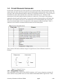
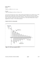
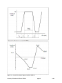
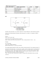
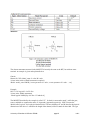
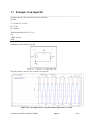
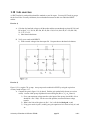
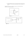
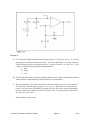
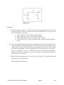
Laboratory Experiment 1 EE348L Jonathan Roderick Onder Oz Tyler Rather Revised by: Aaron Curry University of Southern California. EE348L page1 Lab 1 Table of Contents 1 Experiment #1: SPICE Simulations-I ............................................................................ 4 1.1 Introduction..................................................................................................................................... 4 1.2 First time HSPICE setup on your computer....................................................................................4 1.2.1 To simulate a circuit........................................................................................................... 4 1.2.2 To view/read simulation results of a circuit simulation...................................................... 5 1.3 The Netlist:...................................................................................................................................... 5 1.4 Circuit Elements Statements........................................................................................................... 6 1.5 1.4.1 Independent Sources.......................................................................................................... 7 1.4.2 Dependant Sources.............................................................................................................11 1.4.3 Passive elements................................................................................................................13 1.4.4 Active elements.................................................................................................................14 Command Statements.....................................................................................................................17 1.5.1 Analysis type..............................................................................……………..………….17 1.5.2 Output requested................................................................... …………..………………..19 1.6 Graphical Interface Plots............................................................................ ..……………………..21 1.7 Example of an input file ................................................................................................................ 22 1.8 Reference Reading......................................................................................................................... 23 1.9 HSPICE GUIDELINES REVIEW................................................................................................ 24 1.9.1 To Simulate a Circuit........................................................................................................ 24 1.9.2 To plot the output of a circuit........................................................................................... 24 1.9.3 Some common wave view options....................................................................................24 1.9.4 Some common user problems with SPICE....................................................................... 24 1.9.5 Debugging………………………………………………………………………………..25 1.10 Lab exercises..................................................................................................................................26 1.11 General Report Format Guidelines................................................................................................31 University of Southern California. EE348L page2 Lab 1 Table of Figures Figure 1-1: An independent voltage and current source…………………………………….. ................... 6 Figure 1-2: A transient plot of a sine wave produced by a SIN source…………... ................................ 9 Figure 1-3: A transient plot of a pulsed wave produced by a PULSE source....................................... 10 Figure 1-4: A transient plot of a piecewise linear plot produced by a PWL source………….…….…... 10 Figure 1-5: A schematic representation of r,c,l passive elements….................................................... 13 Figure 1-6: A schematic representation of a diode............................................................................... 14 Figure 1-7: A schematic representation of a BJT………………….……………….................................. 15 Figure 1-8: A schematic representation of a MOSFET…………........................................................... 16 Figure 1-9: A schematic representation of the sample HSPICE input file............................................. 22 Figure 1-10: A transient plot of the input and output nodes from the sample HSPICE input file........... 22 Figure 1-11: A circuit schematic for lab exercise 1…............................................................................. 26 Figure 1-12: A regular 741 op-amp. ................................................................................................... 28 Figure 1-13: An equivalent circuit for Figure 1-12 to be used in HSPICE. …………….………………... 28 Figure 1-14: A circuit schematic for lab exercise 2................................................................................. 29 Figure 1-15: A circuit schematic for lab exercises 3&4........................................................................... 30 University of Southern California. EE348L page3 Lab 1 1 Experiment #1: SPICE Simulations Part I 1.1 Introduction: This experiment is designed to familiarize the student with SPICE. SPICE simulations will be needed for prelabs and projects contained in this lab manual. Spice is an acronym for Simulation Program with Integrated Circuit Emphasis. SPICE is a computer aided design (CAD) tool that should be used to support design and should never be used in place of traditional design methods. Design by SPICE is a trap that many circuit designers fall into and it causes a designer to lose the insight that makes one truly successful. There are many different variations of SPICE that are produced by companies. Two of such versions are LTSPICE (provided for free by Linear Technology) and PSPICE (provided for free by Cadence Design Systems). Another very popular version is HSPICE, which is distributed by Synopsis and whose license has been purchased by USC. The most powerful version of these is HSPICE and thus this lab will provide all SPICE code in HSPICE. However, if a student wishes to use another version of SPICE, they are free to do so. For the most part, SPICE code is universally accepted by SPICE engines. However, there are some differences in available commands and syntax from version to version. Therefore, if any problems are encountered by the version of SPICE you are using, you need to look at its reference manual to make sure you are using it properly. Links to the SPICE manuals for HSPICE, LTSPICE and PSPICE are provided in the “references” section at the end of this lab and are also posted on the course website. 1.2 First time HSPICE setup on your computer: NOTE: Text in the courier font signifies Unix command line input. 1) Log in to your campus Unix account using putty, xwin, or a vncserver/vncviewer. 2) Create a new directory to be used for HSPICE (mkdir hspice). 3) Create a setup file using a text editor such as emacs (emacs setup). 4) In the setup file add the following three lines: source /usr/usc/hspice/2010.03-SP1/setup.csh alias wv /usr/usc/wave_view_analyzer/c2009.03/sx_c2009_03/bin/wv alias distill /usr/usc/acrobat/4.0/bin/distill 5) Save and close the setup file. Now, in the command prompt, source it (source setup). NOTE: Each time you log on and open the hspice directory you will need to source the setup file to use the hspice, wv, and distill commands. 6) You are now ready to run HSPI CE and use WaveView Analyzer. 1.2.1 To simulate a circuit: With SPICE you will need to first create a netlist. A netlist is a text file that describes the circuit and analysis desired. You then simulate the netlist and store the results in an output file. After simulation you are able to view the results from the analysis requested by either viewing the output file or using WaveView Analyzer. 1) Write a netlist using a text editor such as emacs and save it as a .sp file (emacs circuit.sp). University of Southern California. EE348L page4 Lab 1 2) Use the hspice command to simulate your circuit (hspice circuit.sp. If you want to save your output operating point in the file named circuit.out, then use the following command: hspice circuit.sp > circuit.out). 3) Read circuit.out to see if there are any errors or warnings. You must fix the errors while warnings may be ignored depending on severity. This can be done with the more command (more circuit.out). 1.2.2 To view/read simulation results of a circuit simulation: 1) An “.op” analysis will require you to read the output file (circuit.out) to determine the results of this analysis. 2) To view your simulation results, use the .opt post option (sometime use the .probe command as well) to save the data that can be viewed using WaveView Analyzer. WaveView Analyzer can be opened using the wv command (wv &). More on this later. 1.3 The Netlist: This is a model of a typical SPICE input file. _____________________________________________________________________________________ Title (This must be the first line) * Description of the circuit’s function Options Circuit Elements (three kinds) -Sources -Passive Circuit Elements -Active Circuit Elements Model Statements Analysis Requested Output form Requested .END (Before saving the file, make sure to press return once, and only once, after you type this statement) _____________________________________________________________________________________ The “ * ” denotes a comment, description, or statement added by the writer of the spice code. Any designated line with “ * ” at the beginning will be skipped by the complier and will not have an effect on the actual code. Any descriptions or comments can be omitted and the program will execute the exactly the same way. Any comments, descriptions, or statements are for nothing more than the convenience of the reader. The “Circuit Elements” category describes all the physical components that are contained in the circuit schematic. “Analysis Requested” and “Output form Requested” are tools that are implemented in order to view a desired response from the circuit. The “.end” statement tells the compiler that the input file is finished. Don’t worry too much about capitalizing letters, SPICE is case insensitive. University of Southern California. EE348L page5 Lab 1 1.4 Circuit Elements Statements: Each element is described to spice in the input file by an element statement. These statements contain the element name, the nodes where the element is located, and the physical characteristics of the element. The first letter in the element statement identifies what type of element the statement is for. The next two (two terminal device), three (three terminal device), four (four terminal device), etc., characters of the statement are for the node numbers that the terminals are connected to. The last part of the statement contains the physical model of the element. If certain device physical characteristics are left blank, then SPICE has a set of default values that it will automatically use. Even though SPICE has some default values for a limited number of device characteristics, some parameters cannot be left blank. Table 1.1 contains a list of some basic elements and the letter that is used to identify them: These elements fall into three different categories. Signal Sources, Passive Elements, and Active Elements. 1.4.1 Independent Sources: Three independent sources can be used in SPICE simulations. A DC source, a frequency-sweeping AC source, and time varying TRAN source can all be modeled with standard SPICE signal sources. Each University of Southern California. EE348L page6 Lab 1 source can either supply current or voltage. Different types of sources are used for different types of analysis. Table 1.2 lists the different element statements for independent sources and the analysis type that is typically used with each. Each element statement has an array of characters that represent different characteristics of the source. The characters are separated by a space so that the compiler knows that the user is done describing one aspect and starting another. In the element statements, the first letter depicts if the source delivers voltage or current with a V or I, respectively. The first letter is followed by the name of that source. Each source has to have a different name and they can be up to seven characters long. Next, the n+ and n- denote the node number of the positive and negative terminal, respectively. You will assign numbers (alphabetic characters are also valid in SPICE) to all the nodes in your circuit when writing an element statement. You may number (or name) them anyway you wish, with the exception of ground. SPICE interprets node zero as the ground. The type of signal is identified after the node numbers. An example of each will be demonstrated. DC: Generic statement: Vname n+ n- DC value Example: V1 1 0 DC 10V This is a DC voltage source with a value of 10V named “1” and its connected with its positive terminal at node 1 and its negative terminal at node 0 (ground). The name is arbitrary; you can call it anything you want. AC: Generic statement: Vname n+ n- AC (mag phase) Example: University of Southern California. EE348L page7 Lab 1 Vnew 5 0 AC (5V 2) This statement describes a frequency-swept AC source called “new” that is connected to nodes 5 and 0, has a magnitude (mag) of 5V, and contains phase shift of 2 degrees. The phase can be left blank and SPICE will assume a zero degree phase shift. SIN (TRAN): Generic statement: Vname n+ n- SIN (Vo Va freq td damping) Example: Vinput 2 1 SIN (0V 5V 10e3 5e-3 0 0 0) Vo is the initial voltage. Va is the voltage amplitude. freq is the frequency in Hz. td is the time delay in seconds. damping is the decay constant in 1/seconds. This element statement describes a sinusoidal signal named “input” at it is connected between nodes 2 and 1. The signal has an initial voltage of 0V and a magnitude of 5V. It has a frequency of 10kHz and a time delay of 5milliseconds. The signal has no damping factor. If the statement does not contain values for td or damping, then spice assumes a value of zero for both. PULSE (TRAN): Generic statement: Vname n+ n- PULSE (V1 V2 td tr tf PW T) NOTE: tr and tf are swapped when declaring a pulse in PSPICE. Example: V50 15 0 PULSE (2 5 0 2e-3 4e-5 5 10 0) V1 is the lower voltage value. V2 is the upper voltage value. td is the time delay in seconds. tr is the time in seconds it takes for the pulse to rise. tf is the time in seconds it takes for the pulse to fall. PW is the pulse width of the peak value (or the time the pulse remains at the upper voltage value in seconds). T is the time of one pulse period in seconds. The example details a pulse named “50”. It is connected to nodes 15 and 0. The pulse has a lower voltage value of 2V and an upper value of 5V. The time delay is zero seconds, while it takes 2ms and 40µs for the pulse to rise and fall, respectively. The pulse spends 5 seconds at 5V and has a total period of 10 seconds. University of Southern California. EE348L page8 Lab 1 PWL (TRAN): Generic: Vname n+ n- PWL (t1,v1 t2,v2…tn,vn) Example: V100 25 10 PWL(0,0 3e-3,5V 6e-3,5V 10e-3,-3V) To use a piecewise linear source, state a voltage and the corresponding time you wish the source to reach that value. In the example above at time 0, the source will have a value of 0V. The source will then perform a linear increase for the next 3ms till it reaches 5V. The next point given has the same voltage value, so the source will have the value of 5V for the next 3ms. The source will then follow a linear degradation till it reaches –3V four milliseconds later. Graphs of the time varying signals: University of Southern California. EE348L page9 Lab 1 University of Southern California. EE348L page10 Lab 1 1.4.2 Dependant Sources: Dependent sources will be covered in more detail in the second lab. They are introduced in this part. If you have a voltage dependent source there are four nodes in the command. If you have a current dependent source there are two nodes and a voltage source in the command. The first two nodes of any dependent source, n+ and n-, represent the node numbers for the positive and negative ports of the output. (NOTE: current flows from the positive port to the negative port of sources.) If you have a voltage dependent source, the second set of node numbers represents the positive and negative nodes of source’s reference voltage. If you have a current dependent source, the current through the voltage source represents the controlling current. An example of each will be demonstrated. VCVS: Generic statement: Ename n+ n- p+ p- A <MAX=val> <MIN=val> Example: Eone 2 3 1 0 50 MAX=5 MIN=0 In the example, the VCVS is named “one”. Its output is connected between nodes 2 and 3. The controlling, or reference, voltage is between nodes 1 and 0. Its gain is 50. The maximum value is 5V and the minimum value is 0V. VCCS: Generic statement: Gname n+ n- p+ p- G <MAX=val> <MIN=val> Example: Gm1 vout vs vin vs 50m In the example, the VCCS is named “m1”. Its output current flows from node vout to node vs. The controlling, or reference, voltage of the is between nodes vin and vs. Its gain is 50 millisiemens. CCVS: Generic statement: Hname n+ n- vsource R <MAX=val> <MIN=val> Example: H1 10 0 vcontrol 1k In the example, the CCVS is named “1”. Its output is connected between nodes 10 and 0 (ground). The controlling, or reference, current flows through vcontrol. Its gain is 1kiloohms. CCCS: Generic statement: Fname n+ n- vcontrol A <MAX=val> <MIN=val> University of Southern California. EE348L page11 Lab 1 Example: Fmirror vMirrorP vMirrorM vMirrorControl 2 In the example, the CCCS is named “mirror”. Its output current flows from node vMirrorP to node vMirrorM (remember SPICE is case insensitive). The controlling, or reference, current flows through vMirrorControl. Its gain is 2. Scale-Factors and Units In SPICE When dealing with units, there are certain scale-factor abbreviations that SPICE will recognize. The acceptable abbreviations for HSPICE are listed in table 1.3. SPICE does not require you to label the units, however here are the acceptable unit abbreviations. It is recommended to NOT specify the units since they can be confused for a scale-factor (see caution below). Caution: If not caught, SPICE has a really fatal flaw. If you notice, the abbreviation for Farads and femto are both “ F ”. This can be a cause for real heart burn. If you were to label your capacitance value 1F thinking this represents one farad, you would soon find out that spice interprets this as 1 femto farad (1e-15 Farads). Again, it is recommended to just not specify the units. Another common mistake is mixing up mega with milli. For example if you want to make a resistance of 1 mega-ohms and use m instead of meg, you will create a resistance of 1 milli-ohms. University of Southern California. EE348L page12 Lab 1 1.4.3 Passive elements: Passive element statements are very similar to DC sources. The first letter indicates the passive element that is being used. The letters for a standard resistor, capacitor and inductor are listed in table 1.1. A schematic diagram of each is shown below. The schematic diagrams accompanied by a generic statement, an example statement and a brief explanation. Resistor: Generic: Rname n+ n- value Example: R1 5 0 10k The example depicts a resistor named “1”, which is connected between nodes 5 and 0 (ground). It has a value of 10k Ohms. Capacitor: Generic: Cname n+ n- value [IC=initial condition] Example: Cload 50 0 10u [IC=0.5V] This example is a capacitor named “load” connected at nodes 50 and 0 (ground) and it is 10 microfarads. This capacitor also has a 0.5V initial condition. This means that the capacitor has an initial voltage at time equal to zero. If the “[IC=initial condition]” part is left off, SPICE will assume that the initial voltage on the capacitor is zero volts. Inductor: Generic: Lname n+ n- value [IC=initial condition] Example: Lfeedback 50 0 1 University of Southern California. EE348L page13 Lab 1 This is an example of an inductor named “feedback”. It is connected between nodes 50 and 0 (ground) and has a value of 1 Henry. This particular inductor has a 0A initial condition. 1.4.4 Active elements: You will be using these elements in labs later in the semester. They are introduced here. The three basic active elements needed for this class are the diode, BJT and the MOSFET. The element statements for active devices are really similar to passive. The fundamental difference is that the BJT and MOSFET are three and four terminal devices, respectively. The physical characteristics can also be a little more complicated. Other than that, active elements follow the same basic element statement format. The first letter identifies the device type, the next three statements are for the node numbers (only two in the case of the diode), and the last part of the statement contains the physical characteristics. Since active devices have complicated physical characteristics a “.Model” Statement is used. An example of a diode, BJT and MOSFET are all show below. To better illustrate this technique, they will have an accompanying explanation. Diode: Generic: Dname a c model_name *(Later in the netlist a .Model statement is required.) .Model model_name D [certain parameter#1=value certain parameter#2=value … etc ] Example: Drec 2 3 fermi *(Later in the .Model statements.) .Model fermi D [Is=150pA n=1.2] This example is of a diode named “rec”. It is connected between nodes number 2 and 3. This diode references its physical characteristics from a .Model statement called “fermi”. In this particular example the only parameters dictated to Spice are Is and n. More parameters can be specified if desired. Table 1.5 is a list of typical parameters specified for a diode and the default setting for each. University of Southern California. EE348L page14 Lab 1 BJT: The BJT element statement is very similar to the diode. The main difference is that it has three terminals instead of two. Other than that, the structure of the statement is very similar. An example of a NPN is done below. Generic: Qname C B E model_name *(Later in the netlist a .Model statement is required.) .Model model_name NPN [certain parameter#1=value, certain parameter#2=value … etc ] Example: Q1 3 14 5 normal *(Later in the .Model statements.) .Model normal NPN [Is=3e-14, Bf=150, Vaf=30V ] The example statement describes a BJT with its collector connected at node 3, base connected at node 14, and emitter connected at node 5. It references the “.model” statement called “normal” for all the physical characteristics. “normal” indicates to Spice that the BJT called “1” is an NPN transistor and gives some associated characteristics. The “.Model” statement is easily modified to change the transistor to a PNP type. Simply replace the NPN with PNP in the statement. Table 1.6 give some basic characteristics variables for a typical BJT and the default values associated with each. University of Southern California. EE348L page15 Lab 1 MOSFET: The element statement structure for the MOSFET is basically the same as the BJT, but with one more terminal. An example is given and explained below. Generic: Mname D G S B Model_name L=value W=value *(Later in the netlist a .Model statement is required.) .Model model_name NMOS [certain parameter#1=value, certain parameter#2=value … etc ] Example: M55 3 15 0 0 typical L=1u W=20u *(Later in the .Model statements) . Model typical NMOS [kp=10u Vto=1.5 lambda=0] The MOSFET described by the example is called “55”. Its drain is connected to node 3, while the gate, source, and bulk are connected to nodes 15, 0(ground), 0(ground) respectively. SPICE sources the .Model called “typical” for its physical characteristics. The new addition of L and W describe the physical dimensions of the device. L stands for the length of the channel, while W stands for the width. The type University of Southern California. EE348L page16 Lab 1 of MOSFET is identified in the “.model” statement. In this example the MOSFET is a NMOS, but replacing the “NMOS” part in the statement with “PMOS” will change the type of MOSFET from NMOS to PMOS. A table of other typical MOSFET characteristics and their default values are listed in table 1.7. 1.5 Command Statements: Once you have entered all the element statements in the input file, you have to enter the command statements. These command statements tell SPICE exactly how you want to simulate the circuit and present the data. As opposed to element statements, all command statements begin with a period. 1.5.1 Analysis type: Once the element statements are complete, the analysis that is to be done needs to be specified to SPICE. This is done with an analysis request statement. When creating an input file, you must decide from the start what type of analysis you want to perform. As listed in table 1.2, some independent sources only work with certain types of analysis. There are four basic types of analysis to choose from: DC operating point, DC sweep, AC frequency response, and transient response (TRAN). An example of each analysis request statement is done below. DC operating point requested: .OP The .OP command is used when you want to know the DC operating point node voltages, element currents, power dissipation, etc. It gives the DC information of the circuit without sweeping anything. DC sweep: Generic statement: .DC source_name starting_value ending_value step_value A DC sweep is done for many reasons. For example, you would use a DC sweep if you wanted to see the different responses of a circuit for different biasing conditions. Example: .DC power 0V 5V 0.1V University of Southern California. EE348L page17 Lab 1 In the example the “.DC” analysis command instructs the source named “power” in the circuit to start at 0V and increase its values by increments of 0.1V until it reaches a value of 5V, then it stops. AC frequency response: Generic: .AC type number_of_points frequency_start frequency_stop The “.AC” command does not need the name of the source. An AC source is the only source that allows for this type of analysis, so HSPICE will implement this analysis to the AC source in the circuit automatically. Following the “.AC” command are statements that indicates the way points are taken and the number of points taken, respectively. Finally, the starting and ending frequencies are listed. There are three different types of AC frequency responses. The difference deals with how the points are taken. You can specify the following types: DEC (points are spaced logarithmically by decade), OCT (points are spaced logarithmically by octave), or LIN (points are linear spaced). Example of the three different types: .AC DEC 100 2k 1e6 .AC OCT 1000 2k 1e6 .AC LIN 50 500 550 The first “.AC” command depicts a statement that performs a frequency sweep that takes 100 points per decade. The analysis starts at 2kHz and ends at 1MHz. The other two statements follow the same format. Transient response: Generic: .TRAN step_time stop_time The “.TRAN” analysis is preformed when the response of the circuit with time is desired. For example, a transient response request would be used if you wanted to see the time it takes a capacitor to charge or discharge. Caution: For correct data collection, make sure that the smallest step time in the transient command is equal to or smaller then the fastest change in your signal. You must also make sure that the transient time complements the source, or you will not be able to see the simulated results. Example: .TRAN 10n 10m This example simulates the circuit for 10ms and takes data points every 10ns. Transfer Function: Generic: .TF V(node) source University of Southern California. EE348L page18 Lab 1 The .TF analysis is useful for finding ‘small signal’ gain and input/output impedances. This will make more sense later in the semester. Example: .TF V(out) Vin .TF V(2,1) Vin .TF I(Rout) Vin These examples all compute the DC small-signal transfer functions for different outputs with respect to Vin. The first example finds the transfer function from the node called “out” to Vin. The second example finds the transfer function from the differential voltage from nodes 2 to 1 to Vin. The third example finds the transfer function from the current in the resistor called “out” to Vin. 1.5.2 Output requested: With SPICE you can request the data collected to be in the form of data points or as a plot. This is done with a “.PRINT” or “.PLOT” statement. The type of print or plot statement depends on what type of analysis you requested. Table 1.8 lists these statements. You will be able to view the data collected from the Print and Plot requests in the output file that is created once you simulate the input file through SPICE. The Probe statement tells Spice to save information but not output it. HSPICE usually saves all voltages and SUPPLY currents, but to save information about variables the .PROBE statement should be used. The output gives information on what you are measuring (you can measure voltage, voltage difference, or current through any element) and the node number where you want to observe the activity of the circuit. You many request data from multiple outputs, just separate the “output” requests with a space. Table 1.9 lists different “output” statements that may be used to measure voltage, voltage difference, or current in a circuit. University of Southern California. EE348L page19 Lab 1 Some examples are done below. Probe: Generic: .Probe output Example: .Probe ac gain = par(‘20*log10(v(out)/v(in))’) .Probe dc I(Rout) The first example will save the ac results of the gain of the transfer function v(out)/v(in) in db. The second example will save the dc current through the resistor “out”. Print: Generic: .PRINT type output Example: .PRINT DC V(out) This example will print the values of the node voltage called “out” from the DC sweep in a table in the output file. Plot: Generic: .Plot type output Example: .PLOT AC I(R10) This example will plot the values of the current through the resistor called “10” from the ac sweep in the output file. Special “output” requests: Some special “output” requests can be made for AC simulations. Just switch the identifying letter (V or I) in the “output form” listed above with a new abbreviation listed in table 1.10. University of Southern California. EE348L page20 Lab 1 After you have entered all the elements, analysis, and output request you must end the input file with an “.END” statement. Make sure to press return after you have typed your .END statement. Not doing this sometimes hangs up SPICE. 1.6 Graphical Interface Plots: Again, HSPICE plots are very crude and not the most presentable. There are tools that you can use to plot the data once you have collected it. You can use the “.PRINT” statement, then copy and paste the output data into excel or an equivalent and plot it that way. There are also graphical interface programs designed to plot the data stored in you output file automatically. One such program is “WaveView Analyzer”. If you want to use WaveView Analyzer you must include the statement “.opt post” right before your element statements. This will save all node voltages by default (but not element currents or variables). If you are using WaveView Analyzer and you just want to plot node voltages, then you don’t need to include any “.PLOT” or “.PRINT” statements. If you would like to plot element currents or variables, then you will need to use the “.PROBE” statement. To open WaveView Analyzer after a simulation use the following command: unixprompt: wv & The ampersand allows you to continue to use the unix machine and make changes to your *.sp file and resimulate while WaveView Analyzer remains open. Be sure to reload the waveform in WaveView Analyzer if you do so. Once you have WaveView Analyzer open, you will need to add the simulation data to be plotted. You will open three different file types depending on which type of analysis you ran. If you ran a .DC, you will open circuit.sw0. If you ran a .AC, you will open circuit.ac0. If you ran a .TRAN, you will open circuit.tr0. Once the file is loaded, double click on the file name in the ‘Output View’ sub-window and then click on ‘toplevel’. Below, there will be listed all the available plots (node voltages, and if .PROBE was used, element currents and variables). There is much to learn in WaveView Analyzer and the more one uses it, the better one gets. For printing, see section 1.9: HSPICE Guidelines Review. University of Southern California. EE348L page21 Lab 1 1.7 Example of an input file _____________________________________________________________________________________ Example input file *This must be the first line of the file* .opt post * Vs 2 0 SIN ( 0V 1V 10k) R1 2 1 10k D1 1 0 diode * .MODEL diode D (Is=2E-13 N=1.1) .OP .TRAN .01m 1m .END Note: SPICE is case insensitive. A Schematic of the example input file. The plots of nodes 1 and 2 as seen in WaveView Analyzer. Figure 1.10. The output (node 1) is in blue and the input (node 2) is in red. University of Southern California. EE348L page22 Lab 1 This lab is no way intended to be a SPICE manual. This introduction only covers the basics that a student will need to run SPICE. Other published material, such as the ones in the reference reading, on SPICE should be consulted for a better understanding. 1.8 Reference Reading 1. Gordon W. Roberts and Adel S. Sedra. SPICE. Second edition. New York: Oxford Press, 1997. 2. Marc E. Herniter. Schematic Capture with MicroSim Pspice. Third edition. Upper Saddle River, New Jersey: Prentice Hall, 1998. 3. HSPICE user manual. http://jcatsc.com/media/ee348/Labs/ee348_2001-4_hspice.pdf 4.LTSPICE IV user manual. http://jcatsc.com/media/ee348/CADandLabs/LTspiceIVRef.pdf 5. PSPICE user manual. http://jcatsc.com/media/ee348/CADandLabs/PSpiceRef.pdf University of Southern California. EE348L page23 Lab 1 1.9 HSPICE GUIDELINES REVIEW: 1.9.1 To Simulate a Circuit: 1) Write a netlist using a text editor such as emacs and save it as a .sp file (emacs *.sp). 2) Use the hspice command to simulate your circuit (hspice circuit.sp > circuit.out). 3) Read circuit.out to see if there are any errors or warnings. You must fix the errors while warnings may be ignored depending on severity. This can be done with the more command (more circuit.out). 1.9.2 To plot the output of a circuit: 1) To plot the results of a simulation, run WaveView Analyzer (wv &) at the unix prompt. (Make sure you have used the .opt post option or the .probe command.) 2) When WaveView Analyzer opens, go to FileImport Waveform File. 3) Select the output file(s) you want to view. If you ran a .TRAN, you will open filename.tr0. If you ran a .DC, you will open filename.sw0. If you ran a .AC, you will open filename.ac0. If you ran a .OP or a .TF, the outputs can be viewed in the output file. 4) Select the data you wish to be plotted. 1.9.3 Some common wave view options/printing: 1) To add a cursor, go to AxesCursorAdd Cursor 2) To change the background color to white, go to ConfigPreferences. Click on the Waveview tab. For ‘Waveview Background’ select ‘White’. 3) To export the wave view as a postscript, go to FilePrint. Near the bottom in the ‘PostScript Output File’ check the box marked ‘Print To File’. In the ‘Output Path’ text box name your file filename.ps in the path you wish. Click ‘Print’. 4) To convert from .ps to .pdf, you will need to run the distill command (distill filename.ps). This will create filename.pdf. NOTE: Wave View has many tools and options. The more you use and play with it the better you will get with it. 1.9.4 Some common user problems with SPICE: 1) Typing “op” instead of typing “.op”; typing “tran” instead of “.tran” etc. 2) Missing “.end” at the end of the netlist. Please make sure that you hit carriage return (the “enter” key on the keyboard) after the .end statement. 3) Mistyping the netlist or using letters instead of digits. 4) Incorrect syntax for source statements in HSPICE. 5) Having floating nodes in the netlist. (To simulate an open, use a very large resistor, like 1 gigaohm, where the open is.) University of Southern California. EE348L page24 Lab 1 6) Incorrect number of arguments for control statements in SPICE. An example of an incorrect SPICE control statement is the following, which is missing one of the parameters of the PULSE statements (see page 5 of this lab). “V1 1 2 PULSE 0 5 1m 1p 5m 10m” 7) Using the wrong units. For example, user types “1M” to specify 1e6, which SPICE interprets as 1e-3 (1 milli). 8) Using the wrong analysis type for the sources used. For example, the user wants to run a .AC analysis but uses a SIN source (which should be used for a .TRAN analysis). 9) Specifying the wrong sweep values. For example, the 3-db value is 1kHz but the user sweeps from 10kHz-1GHz. 10) The user forgets to include the ground node (0) in their netlist. 1.9.5 Debugging 1) Debugging problems with SPICE simulations is very similar to debugging computer programs. It is important to follow an orderly procedure. 2) Make sure that there are no typographical errors. See the section on common user problems in SPICE. 3) Make sure that the syntax of SPICE commands in the netlist is correct. 4) Make sure that the circuit represented in the netlist is what you want. 5) Make sure that the SPICE netlist (the circuit.sp file) has the correct analysis statement with the correct parameters and the correct type of source (for example, a source with “AC magnitude and optional phase” for an AC analysis”. University of Southern California. EE348L page25 Lab 1 1.10 Lab exercises A SPICE netlist for each problem should be attached to your lab report. You may NOT work in groups for the first 2 labs! You may collaborate, but each student must turn in their own individual SPICE netlists. Exercise 1) A. Calculate (by hand) the volages at all the nodes and the current through resistors R3, R4, and R5 in figure 1.11. R1=2k, R2=500, R3=2k, R4=1.5k, R5=1k, R6=10k, R7=2.2k, R8=200, V1=3.3V, V2=5V. 1) Show hand calculations. B. Verify your results with HSPICE. 1) Print out node voltages from the output file. Compare them to the hand calculations. Exercise 2) Figure 1.12 is a regular 741 op-amp. An op-amp can be modeled in SPICE by using the equivalent circuitry found in Figure 1.13. A. Compute the gain in figure 1.14 (by hand). Find the gain symbolically (do not use resistor values). Assume ideal op-amp impedances but not ideal gain (Rin=∞, Ao=Ao, Rout=0). 1) If we want maximum voltage transfer to the input of the op-amp, should R1>>Rs or should R1<<Rs? Why? For the rest of the problem, assume maximum voltage transfer. 2) What is the limit of the gain as Ao∞? Let’s call this the ideal gain, or Ai. 3) Using your results in part 2, modify your gain equation to be in terms of only Ai, and A0. University of Southern California. EE348L page26 Lab 1 4) What is the limit of the gain as Ao>>Ai? How much larger than Ai should Ao be for the gain to be within 1% of Ai? This exercise should give us an idea of either the lower limit of the gain of an op-amp (Ao) for a particular ideal gain, or the upper limit of the ideal gain for a particular op-amp gain (Ao). B. Given the circuit resistor values in figure 1.14, find: 1) The ideal gain of the circuit (Ai). 2) The actual gain of the circuit if Ao=Ai, 10Ai, and 100Ai. C. Use the equivalent circuit (figure 1.13) and HSPICE to verify your answers you found in part (B). Using a .TRAN analysis, let Vs be a SIN source with amplitude of 50mV and a frequency of 500Hz. Use the .opt post option and WaveView Analyzer for your plots. 1) What should tstep be if we want 1000 points/period? 2) What should tstop be if we want to plot 2 periods? 3) Simulate for Ao=Ai. Plot Vo and Vs on the same panel and attach a curser to verify the gain calculated in part B. 4) Repeat for Ao=10Ai and Ao=100Ai. D. It should be noted that as Ao∞, the two input nodes approach the same value. Repeat the simulation from part (C) but this time plot each input node of the op-amp. Note the changes when Ao goes from Ai to 100*Ai. E. Now, do not let Rout=0, but let Ao∞ (as we just saw, this implies each input node to the opamp are at the same voltage). Find the following gains in figure 1.14 (by hand) symbolically: 1) Vo/Vs. Should this be any different from Vo/Vs found in part (A)? Why? 2) Vz/Vo. 3) Vz/Vs. Is it necessary to go through KVL/KCL for this if we have already found the previous two? Why? Hint: A good way to check your work is to realize that (Vz/Vs)*(Vo/Vz)=Vo/Vs. 4) Is Vz/Vs larger or smaller than Vo/Vs? By what factor? 5) If Rout<<(R2+Rf), what is Vz/Vo? 6) If Rout~(R2+Rf), what is Vz/Vo? 7) If Rout>>(R2+Rf), what is Vz/Vo? F. Given the circuit resistor values in figure 1.14, find: 1) R2+Rf. Let’s call this Rseen. 2) The gains Vz/Vo and Vz/Vs if Rout=Rseen/100. 3) The gains Vz/Vo and Vz/Vs if Rout=Rseen G. Use the same HSPICE simulation stimulus as in part C with Ao=100*Ai. However, NOW WE WILL ADD +/- RAILS! Let the value of the +/- rails be +/-9V. (See page 11.) 1) Simulate for Rout=Rseen/100. Plot Vo, Vz, and Vs on the same panel. Attach a curser to verify the gains. Given the gains and input amplitude, explain why clipping occurs if it does. University of Southern California. EE348L page27 Lab 1 2) Simulate for Rout=Rseen. Plot Vo, Vz, and Vs on the same panel. Attach a curser to verify the gains. Given the gains and input amplitude, explain why clipping occurs if it does. Hopefully now you see why we want Rout of an op-amp to be much smaller than Rseen! Remember to show all plots in your report. University of Southern California. EE348L page28 Lab 1 Exercise 3) A) Use a transient (.TRAN) simulation on the circuit in figure 1.15 to plot Vo with Vs. Vs is a pulse generating source that alters between 0v and 5v. The source should have a 1ms delay, 5ms pulse width, 10ms period, and a rise and fall time of 1ps. Using R1=2k and C1=.1u, plot Vo vs. Vs for a tstep of 1u and the following transient simulation times: 1) 30ms 2) 300ms 3) .3ms B) Do the results differ when using three different simulation times? Why is it important to make an educated decision when choosing a simulation time for your simulation? C) The time constant of a first order system refers to the time it takes the system to reach within 1/e of its final value when the input is a step (Vout=Vfinal*[1-e-1]). What is the time constant of this circuit? Verify this value with HSPICE by adding a curser to WaveView Analyzer and finding the time it takes for the output to reach 63% of its final value. (You may need to zoom in the xaxis, time, to see this value.) Include all plots in your report. University of Southern California. EE348L page29 Lab 1 Exercise 4) A) Using the schematic in figure 1.15, peform an .AC analysis to plot a frequency sweep of Vo with 100 points per decade. Replace Vs with an ac source with a magnitude of 1V. Be sure to make the x-axis logarithmic in your plots. 1) Let R1=1k and C1=100p. Sweep from 10Hz-10kHz 2) Let R1=100k and C1=100n. Sweep from 10Hz-10GHz 3) Why did both of these sweeps fail to show a valid .AC sweep? 4) Let R1=100 and Cl=1p. Sweep from 10Hz=10GHz. What is the problem with this sweep? B) One can see that choosing the correct frequency range optimizes the results. One common error ee348L students make is submitting poor plots. An original sweep from ‘DC to daylight’ can be a good way to get an idea of what frequency range is appropriate to sweep; however, this original plot should not be submitted. Find the -3db frequency of the circuit in Figure 1.15 from part A, number 1. (remember, 2*π*f-3db=w-3db). Run another ac sweep that sweeps two decades before and two decades after the -3db frequency. Be sure to make the x-axis logarithmic (right click on the scale in WaveView Analyzer). C) What should be the magnitude of the value of Vo at the -3db frequency? Using the plot from part B, add a curser at the -3db frequency. Include all plots in your lab report. University of Southern California. EE348L page30 Lab 1 1.11 General Report Format Guidelines This guideline should be followed from a problem to problem basis for parts 2-5. For example, start with 1, then for exercise 1, do parts 2-5. Then repeat for each other exercise. Then wrap it up with parts 6-7. 1. Introduction Explain what the lab is about. Describe the circuits being built in terms of structure and purpose. Also talk about what is being investigated. For Each Exercise 2. Procedure Step by step talk about what was done and show diagrams of the circuits. 3. Data Present data taken during the lab. It should be organized and easy to read. 4. Questions Answer all the questions in the lab. 5. Discussion Discuss the results you obtained. What significance is there in the results? How do they help your investigation? Explain the meaning; the numbers alone aren’t good enough. 6. Conclusion Wrap up the report by giving some comments on the lab. Do the results clearly agree with what the lab was trying to teach? Did you have any problems? Suggestions? 7. Attachments Attach all hand calculations and SPICE plots necessary. IF A LAB EXERCISE ASKS YOU TO COMPARE YOUR RESULTS WITH YOUR PRE-LAB, INCLUDE YOUR PRE-LAB RESULT IN YOUR LAB REPORT! SIMPLY STATING THEY ARE THE SAME IS NOT GOOD ENOUGH! NOTE: You are turning in lab reports that are to be graded. If you want good marks, be sure to make the reports as neat and aesthetically appealing as possible. If you refer to an attached plot, include the page number. If you refer to a hand calculation, be sure to highlight what you are referring to on the page containing the hand calculation. However, including equations, plots, figures, etc. in the body of your report is good practice. Be sure to include plot titles. Be sure to include axis titles and units. Lab reports are to be typed. HANDWRITTEN REPORTS WILL NOT BE ACCEPTED. LAB REPORTS ARE DUE AT THE BEGINNING OF THE NEXT LAB. THEY WILL NOT BE ACCEPTED IF THEY ARE MORE THAN 15 MINUTES LATE! University of Southern California. EE348L page31 Lab 1