1
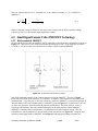
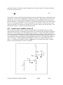
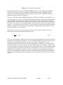
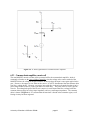
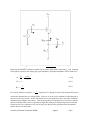
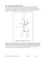
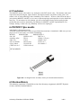
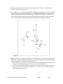
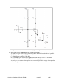
Laboratory Experiment 6 EE348L B.Madhavan Revised by: Aaron Curry University of Southern California. EE348L page1 Lab 6 Table of Contents 6 Experiment #6: MOSFETs .......................................................................................... 4 6.7 MOSFET High-Frequency Model ............................................................................................. 4 6.8 Small Signal Canonic Cells of MOSFET Technology .............................................................. 8 6.8.1 Diode-connected MOSFET........................................................................................................ 8 6.8.2 Common source amplifier canonic cell ...................................................................................... 9 6.8.3 Common drain amplifier canonic cell...................................................................................... 11 6.8.4 Common gate amplifier canonic cell........................................................................................ 12 6.10 Conclusion................................................................................................................................ 14 6.11 MOSFET Spice models..............................................................................................................14 6.12 Revision History ....................................................................................................................... 14 6.13 References ................................................................................................................................. 15 6.14 Pre-lab Exercises ...................................................................................................................... 16 6.15 Lab Exercises............................................................................................................................ 20 University of Southern California. EE348L page2 Lab 6 Table of Figures Figure 6-1: Large signal high frequency model of a MOSFET. .............................................................. 5 Figure 6-2: Low frequency small signal MOSFET model. ...................................................................... 6 Figure 6-3: A MOSFET connected as a diode. ....................................................................................... 8 Figure 6-4: A Common-source amplifier. ................................................................................................ 9 Figure 6-5: A small signal model of a common source amplifier. ......................................................... 10 Figure 6-6: Common drain (or source-follower) canonic cell. ............................................................... 11 Figure 6-7: A common gate canonic cell............................................................................................... 13 Figure 6-8: Pin diagram of the 2N7000 (Courtesy of Fairchild Semiconductor). .................................. 14 Figure 6-9: Circuit schematic for Laboratory experiment 6 pre-lab exercise 1...................................... 16 Figure 6-10: Circuit schematic for Laboratory experiment 6 pre-lab exercises 3, 4, and 5..................... 17 Figure 6-11: Circuit schematic for Laboratory experiment 6 pre-lab exercise 6.......................................18 Figure 6-12: Circuit schematic for Laboratory experiment 6 pre-lab exercises 7 and 8 ......................... 19 University of Southern California. EE348L page3 Lab 6 6 Experiment #6: MOSFETs Dynamic Operation 6.1 MOSFET High-Frequency Model This experiment will build upon the concepts that were presented in the previous lab and introduce dynamic circuits using MOSFETS. In the previous lab, we focused on properly biasing the MOSFET and we learned that the purpose of biasing an analog circuit is so the active devices within the circuit operate in a desirable fashion (linear) on small signals that enter the circuit. Once the MOSFET has been biased in the dynamic linear region, a.k.a. saturation, one may use the small signal model developed to perform dynamic circuit analysis. Signals are perturbations about the bias point (or quiescent point, a.k.a. Q-point) and carry all the important information for your circuit to process. For instance, you might bias your input port at 2V, and then superimpose a 50 mV peak-to-peak sine wave to this bias voltage. Ideally, you would like amplifiers to be perfect linear devices, meaning the output signal is some multiple of the input signal, independent of the input amplitude. There are many ways that information is modulated, but for the purposes of this experiment we will deal will strictly sinusoidal waves. Transistors are normally non-linear devices (recall their I-V characteristics), so the device bias point, and hence the gain, does depend upon the input amplitude. However, by suitably restricting the amplitude of the input swing (using a “small signal”) and correctly biasing the circuit (Q point), the resultant output will show very little distortion, meaning that the non-linear circuit acts approximately linear for smallsignal deviations about the bias point. University of Southern California. EE348L page4 Lab 6 Figure 6-1: Large signal high frequency model of a n-channel MOSFET. The MOSFET high frequency large-signal model is an empirical model and is shown in Figure 6-1. It is called a large-signal model because the values of model elements are dependent on the dc bias voltage and current conditions of the device. In Table 6-1 you will find a list of what each element represents in the MOSFET large signal model. As you can see all elements are physical, unlike the BJT, which will be presented in future labs, where it is based off a Taylor series expansion. The model in Figure 6-1 looks very complicated. This model can be simplified for a first order analysis. If the signal of interest is a “small signal”, the frequency range of interest is small enough and processing conditions are good, then many of the elements in Figure 6-1 maybe neglected for a simplified back of the envelope calculation. For many cases this first order analysis is perfectly acceptable. If conditions arise where the model fails, then the insight learned from it should be built upon and used to accurately account for any second order effects. A simplified NMOS low frequency small signal model is found in Figure 6-2. Table 6-1: MOSFET large-signal high-frequency model parameters University of Southern California. EE348L page5 Lab 6 Figure 6-2: Low frequency small signal MOSFET model. Notice that all the capacitances are neglected in the low frequency model. Therefore, by definition, the validity of the low frequency model is limited to operating frequencies where these capacitors act as open circuits. For the purposes of this lab, the models and theory presented will focus on the NMOS transistor. The following models also apply for the PMOS transistor with the slight modification of reversing the direction of all controlled current sources and branch currents, and a reversal in polarity of all port and branch voltages. Note: The small signal model is just a tool that is used to help circuit designers analyze circuits utilizing MOSFETs. Remember, this tool is only valid if the transistor is operating in the region of validity of its small-signal model. Therefore it should be understood that when using the small-signal model, significant effort has been made to ensure that the signal being processed in the amplifier is not too large, ensuring that the dc-bias conditions are not significantly disturbed. This validates the “small signal” assumptions, allowing the valid linearization of the non-linear characteristics of the device. A large enough signal may cause the transistor to leave its linear region of operation if its signal change has a magnitude large enough to offset the set Q (biasing) point, causing signal distortion. Next, a description of the model and its parameters will be given, and then what is known as the basic MOSFET canonic cells will be present and discussed. One can see from Figure 6-2 that at low frequencies the MOSFET behaves like a voltage controlled current source (VCCS). This is a little different than its cousin, the BJT. It will be presented in later experiments that the BJT is treated like a current controlled current source. The MOSFET takes any modulated signal applied to the gate and multiplies it by the small-signal forward transconductance. Even though the MOSFET and the BJT are very closely related, they have some very distinct differences. The MOSFET has an input resistance that is significantly higher. In fact, at low frequencies the input resistance is infinite. The MOSFET has superior input signal to output current linearity performance. Unlike the BJT, the MOSFET is a majority carrier device. Therefore, the MOSFET University of Southern California. EE348L page6 Lab 6 experiences a negative temperature coefficient. Where any rise in temperature causes the output current of a BJT to rise, the opposite is true for the MOSFET. In terms of power consumption, the MOSFET also outperforms a bipolar device with lower power consumption. About now one might be questioning why BJT transistors are still around if MOSFETS has so many superior performance characteristics. The truth is the MOSFET does yield to the bipolar devices in some analog performance categories. The MOSFET lacks the forward gain and bandwidth t h a t c a n b e a c h i e v e d w i t h e q u i v a l e n t b i p o l a r d e v i c e s . The transconductance generated by a BJT increases linearly with the Q-point current. The small signal forward gain of a MOSFET increases at a factor of the square root of the Q-point current. This equation for the small signal forward transconductance, gm, of a MOSFET is stated in equation 6.1. This equation neglects channel length modulation effects. Therefore, it can be challenging to achieve any appreciable gain out of a MOSFET circuit. gm I D Vgs Q po int W 2 K n I DQ L (6.1) where ID is the internal drain current. One will notice that the small signal model has two dependent current sources. The second one models bulk effects and shows the bulk-to-source transconductance, gmbs. The equation for gmbs is given in equation 6.2. gmbs b gm (6.2) Where λb is known as the channel length modulation factor and it is defined in equation (6.3) b V 2 2VF VT VvsQ (6.3) Where Vθ is known as the body effective voltage, VF is the Fermi potential, and VT is Boltzmann voltage. All three are defined in equations 6.4 through 6.6. V qN A s C ox (6.4) 2 N VF VT ln A Ni (6.5) VT = 0.0259V (6.6) University of Southern California. EE348L page7 Lab 6 The last element that has to be accounted for is the channel resistance, ro. It is defined in equation 6.7. 1 I D ro Vds Q po int I DQ (6.7) V VdsQ VdssQ Where VdsQ and VdssQ are defined as the drain source voltage and the drain saturation voltage, respectively, and Vλ is the channel length modulation voltage. 6.2 Small Signal Canonic Cells of MOSFET Technology 6.2.1 Diode-connected MOSFET As stated in the previous lab, the MOSFET can be connected as a diode and this configuration is shown in Figure 6-3. This circuit is very useful and common when biasing circuits. If you refer back to section 5.6 of lab 5, one can see that every current mirror contains a diode-connected MOSFET. Figure 6-3: A MOSFET connected as a diode. The diode-connected transistor is the simplest canonic cell for the MOSFET. The gate in Figure 6-3 is tied to the drain of the transistor, so it exhibits I-V behavior close to that of a conventional PN junction diode. Tying the gate to the drain effectively makes the MOSFET a two-terminal element. If one refers back to the cross sectional model of a MOSFET given in Figure 5-2, in experiment 5, one can see that a p-n junction is formed between the substrate and the drain. The affect of the n+ source is effectively nullified due to the source and bulk being tied to the same potential. Notice when the MOSFET is connected in this configuration, it is guaranteed to be in its saturation region. This two terminal device may be modeled as a two terminal resistor seen next to it in Figure 6-3. Using the lowfrequency small-signal model of MOSFET from Figure 6-2 and neglecting channel resistance, the University of Southern California. EE348L page8 Lab 6 equivalent resistance of the diode-connected transistor can be found to equal rd. The proof of equation 6.8 is left as a pre-lab exercise. rd 1 gm (6.8) The next three canonic cells that will be presented are known as the common source, common drain, and common gate. All three have applications in analog circuit design. They get their respective names from the way they are connected. With the bulk tied to the source, the MOSFET effectively becomes a three terminal device. Each canonic cell will have a signal input and signal output at one of the terminals. Since we are treating the MOSFET as a three terminal device, one terminal is not used in part of the signal flow and thus is connected to ac ground. This is where the canonic cells get their name. The terminal that is leftover is effectively the common terminal. 6.2.2 Common-source amplifier canonic cell In this section, the common source is explored. Notice that the input is applied to the gate, while the output is taken at the drain. The primary purpose of this cell is to provide small signal gain. Another key characteristic of this topology is its inherent high output resistance. Looking at the small signal model, one can see at low frequency the device effectively has infinite input resistance. Both proofs will be left as pre-lab assignments. The input and output impedance characteristics determine that the common source amplifier is best suited accepting a voltage and delivering a current. This supports the statement made in experiment 5 which explained that the MOSFET is effectively a voltage controlled current source. A common-source amplifier is shown in Figure 6-4. It is assumed the transistor is properly biased, so external biasing (DC) circuitry is neglected. University of Southern California. EE348L page9 Lab 6 Figure 6-4: A Common-source amplifier. Replacing the schematic symbol of an NMOS in Figure 6-4 with the small signal model in Figure 6-2, one can calculate the gain, input impedance, and the output impedance. Figure 6-5 shows a common-source amplifier utilizing the small signal model. However, it has assumed low frequency operation and neglected channel resistance ro. Notice the small signal model in Figure 6-5 neglects to include any voltage source resistance, Rs. At very low frequencies, it can be seen by inspection that the input resistance is infinite, thus neglecting the source resistance is not an unrealistic assumption that is only valid in an academic setting. However, at high frequencies, this assumption fails and one must account for the source resistance for any analysis to be accurate. One can also see, if neglecting channel resistance, that the resistance seen looking into the drain, Rseen, is also infinite at low frequencies. By inspection you will notice that when looking into the drain one is staring at a VCVS whose controlling voltage is grounded when using an ohmmeter. Thus, the output resistance, Rout, is simply RD. The gain of the circuit is not as easily calculated as the input and output resistances, but simple KVL and KCL equations should yield the following result. AV Vo g m RD Vs (6.9) One can see from equation 6.9 that the gain of this amplifier greatly depends on the resistance connected to the drain. Referring back to equation 6.1, one can see that the MOSFET gate aspect ratio (W/L) and the drain current, also determine the gain. This is comforting that a designer has a variety of controllable parameters that can determine the gain of the topology. Unfortunately, it can be seen that some of the variables that control the gain are device fabrication-process dependent. Problems may arise when dealing with process tolerances that can be on the order of ±20%. Another drawback, which was pointed out earlier, is that the transconductance of a MOSFET is well below what can be achieved with other device technologies. Therefore, to achieve comparable gain, more than one stage may be needed. The common-source amplifier example presented here neglected the influence of the MOSFET channel resistance and the external resistance between source and ground. This will be left as a pre-lab exercise. University of Southern California. EE348L page10 Lab 6 Figure 6-5: A small signal model of a common source amplifier. 6.2.3 Common drain amplifier canonic cell The next MOSFET canonic cell that will be presented will be the common drain amplifier, which is commonly referred to as the source-follower amplifier since the voltage at the source terminal of the MOSFET follows the voltage at the gate terminal. In this topology the input is once again applied at the gate. However, the output is now taken at the source. It will be demonstrated that the common drain acts like a voltage buffer. However, one major issue with this circuit arises from the fact that it isn’t a great voltage buffer because it yields a gain that is less than unity. The proof of this is left as a pre-lab exercise. Even though the gain of this circuit is suspect, it can be shown that like a voltage buffer the common drain topology has a large input impedance, and very small output impedance. The common drain is shown in Figure 6-6. It is assumed that the transistor is biased in the saturation region, so all biasing circuitry has been neglected. University of Southern California. EE348L page11 Lab 6 Figure 6-6: Common drain (or source-follower) canonic cell. Replacing the MOSFET schematic symbol with its small signal model, neglecting ro, a n d assuming low frequency operation, the voltage gain, input impedance, and output impedance can be found to be: VO g m R ss V s 1 g m R ss Rin AV R seen (6.10) (6.11) 1 gm For a source-follower, usually R ss (6.12) 1 . Equations 6.11 through 6.14 show the common drain tries to gm emulate the characteristics of a voltage buffer. However, it can be seen in equation 6.10 that the gain of this circuit can never be unity. In fact, the solution for Av presented above was a first order calculation and thus neglected higher order effects. Thus the gain predicted in equation 6.10 is a best case scenario and will more than likely result in a gain that is larger than what you will physically measure in the lab. From what you see in equation 6.10 it will be your job in the pre-lab to speculate where the potential pitfalls may lie in its derivation. University of Southern California. EE348L page12 Lab 6 6.2.4 Common gate amplifier canonic cell The last canonic cell presented in the common gate. Notice in this configuration that the input is connected at the source, while the output is taken at the drain. The common gate finds utility as a current buffer. One will discover that it has unity current gain, low input resistance, and high output resistance. Once again the proof is left as a pre-lab exercise. A circuit schematic of a common gate configuration is shown in Figure 6-7. Note: Once again biasing has been neglected. Figure 6-7: A common gate canonic cell. The input resistance and output resistance have already been derived from other canonic cells. The input resistance is the same as the output resistance of a common drain. The output resistance exactly the same as what was found for the output resistance of a common source. Assuming the internal resistance of the current source is ideal (Rs >> Rin) and if there are no other paths for the current to flow, the calculation of the gain is trivial. One can simply see that the current flowing into the source must equal the current leaving the drain. Hence, the common gate has unity current gain. University of Southern California. EE348L page13 Lab 6 6.3 Conclusion The MOSFET canonic cells behave very analogous to the BJT canonic cells. The absolute values and expressions found for the gain, input resistance, and output resistance may differ, but the point is the canonic cells of both technologies have remarkably close behavior. However, don’t fall in the trap of just replacing MOSFET with BJT, or vice versa, in known topologies and expect the circuit to behave the same way. As one matures in circuit design, you will see that many factors result in topologies that produce the same result are structurally very different for MOSFET and BJT implementation. For example, biasing is dealt with very differently for these two topologies. 6.4 MOSFET Spice models *(this Model is from supertex.com) *Note that usually the W and L values are specified when a transistor is instantiated. Make sure you *use proper size of w=.8e-2 and l=2.5e-6 when instantiating. .MODEL NMOS2N7000 NMOS(LEVEL=3 +Rs=.205 NSUB=1.0e15 DELTA=.1 +KAPPA=.0506 TPG=1 CGDO=3.1716e-9 +RD=.239 VTO=1 VMAX=1.0e7 +ETA=.0223089 NFS=6.6e10 TOX=1.0e-7 +LD=1.698e-9 UO=862.425 XJ=6.4666e-7 +THETA=1.0e-5 CGSO=9.09e-9) * *2N7002 MODEL * Figure 6-8: Pin diagram of the 2N7000 (Courtesy of Fairchild Semiconductor). 6.5 Revision History This laboratory experiment is a modified version of the laboratory assignment 6 (MOSFET Dynamic circuits) created by Jonathan Roderick. University of Southern California. EE348L page14 Lab 6 6.6 References [1] Avant! HSpice User Manual, Version 2001.4, December 2001, posted on EE348L class web site. [2] Avant! HSpice Device Models Reference Manual, Version 2001.4, December 2001, posted on EE348L class web site. [3] Bindu Madhavan, EE348L Laboratory Experiment 3, Spring 2005. [4] Gerald W. Neudeck. Volume II The PN Junction, Addison-Wesley Publishing Company, Reading, Massachusetts, 1989. [5] Ben G. Streetman. Solid State Electronic Devices. Prentice-Hall Inc., Englewood Cliffs, New Jersey, 1990. [6] Richard C. Jaeger. Introduction to Microelectronic Fabrication. Addison-Wesley Publishing Company, Reading, Massachusetts, 1993. [7] S. M. Sze. Physics of Semiconductor Devices. John Wiley & Sons, Inc., New York, 1981. [8] Paul R. Gray & Robert G. Meyer. Analysis and Design of Analog Integrated Circuits. John Wiley & Sons, Inc., New York, 1993. University of Southern California. EE348L page15 Lab 6 6.7 Pre-lab Exercises Note: For Spice simulations, use the model deck for 2N7000 in section 6.4 For Spice simulations, let each Cc be 10uF. Submit plots relevant to each question in your lab report. Figure 6-9: Circuit schematic for Laboratory experiment 6 pre-lab exercise 1. 1) The example of the common-source amplifier in Figure 6-4 neglected any external resistance connected between the source terminal and circuit ground. Figure 6-9 features a common-source amplifier with an external source resistance, Rss. Re-derive the gain, Rseen, and Rout of the common-source amplifier taking into account the external resistance Rss. How did the external source resistance affect the gain of the common- source amplifier? Hint: Rout=Rseen//RD. 2) Figure 6-10 shows a common source amplifier with source degeneration. Rb1 and Rb2 are necessary for biasing the gate of the transistor. Both coupling capacitors isolate the DC operating point of the amplifier with the input and output nodes. A) Assuming the coupling capacitors, Cc, act like a short circuit at the frequency of the input signal, find the input resistance, Rin. B) Now, using this and the result for Rout in pre-lab exercise 1, find an expression for the low frequency zeros caused by each Cc. Note: if we wish to lower the input zero frequency we can simply increase Rb1 and Rb2 by an order of magnitude. University of Southern California. EE348L page16 Lab 6 Figure 6-10: Circuit schematic for Laboratory experiment 6 pre-lab exercises 2-4. 3) Refer to the circuit in Figure 6-10 and neglect the load Rl. A) If the transistor is biased to 1mA of drain current, calculate both the gm of the transistor and the gain using the following values: un=725cm^2/Vs, Rd=1.5k, Rss=500. B) Verify your results in Spice by using the values for Rb1 and Rb2 you found in pre-lab exercise 5 from lab 5 (Vdd=5V). Let Vs be a sine wave with frequency of 10kHz and amplitude of 50mV. 4) Refer to the circuit in Figure 6-10. Now, include resistance Rl. A) What is the gain of the circuit (symbolically)? Hint: Rl can be lumped with RD in parallel. B) What happens to the gain if Rl=RD? C) What happens to the gain if Rl<<RD? D) Calculate the gain of the circuit in Figure 6-10 for the values in exercise 4 and for the following Rl values: 100k, 10k, 1k, and 100. Verify using a transient simulation in Spice. Let Vs be a sine wave with frequency 10kHz and amplitude of 500mV. As can be seen, a common source amplifier does a poor job at providing voltage at the output due to its large output resistance. It is much better suited for providing current at the output. University of Southern California. EE348L page17 Lab 6 5) Refer to the gain equation for a common source amplifier from exercise 1. What are three possible ways to increase the gain? 6) The example of the common-drain amplifier in Figure 6-6 neglected any external resistance connected between the drain terminal and circuit Vdd. Figure 6-11 features a common-drain amplifier with an external drain resistance, RD. Re-derive the gain, Rseen, and Rout of the common-drain amplifier taking into account the external resistance RD. How did the external drain resistance affect the gain of the common-drain amplifier? Hint: Rout=Rseen//Rss. Figure 6-11: Circuit schematic for Laboratory experiment 6 pre-lab exercise 6. 7) Figure 6-12 shows a common-drain amplifier. Rb1 and Rb2 are necessary for biasing the gate of the transistor. Both coupling capacitors isolate the DC operating point of the amplifier with the input and output nodes. Neglect the load resistance Rl. A) If the transistor is biased to 1mA of drain current, calculate both the gm of the transistor and the gain using the following values: un=725cm^2/Vs, Rd=1.5k, Rss=500. B) Verify your results in Spice (both gm and the gain) by using the values for Rb1 and Rb2 you found in pre-lab exercise 5 from lab 5 (Vdd=5V). Let Vs be a sin wave with frequency of 10kHz and amplitude of 50mV. University of Southern California. EE348L page18 Lab 6 Figure 6-12: Circuit schematic for Laboratory experiment 6 pre-lab exercises 7 and 8. 8) Refer to the circuit in Figure 6-12. Now, include resistance Rl. A) What is the gain of the circuit (symbolically)? Hint: Rl can be lumped with Rss in parallel. B) What happens to the gain if Rl=Rss? C) What happens to the gain if Rl<<Rss? D) Calculate the gain of the circuit in Figure 6-10 for the values in exercise 7 and for the following Rl values: 100k, 10k, 1k, and 100. Verify using Spice. As can be seen, a common-drain amplifier does a great job at providing voltage at the output due to its small output resistance. University of Southern California. EE348L page19 Lab 6 6.8 Lab Exercises Note: See section 6.4 for Spice MOSFET model deck for 2N7000. Submit plots relevant to reach question in your lab report. Remember that an amplitude of 50mV corresponds to a Vpp of 100mV. 1) Build the circuit from pre-lab exercise 3 without the load, Rl. Apply a 50mV peak-to-peak 10kHz sinusoidal signal at the input. Measure the output signal at the drain of the MOSFET. Do your results agree with your calculations and Spice results from pre-lab question 4? Why or why not? Hint: use a potentiometer for Rb2 and adjust it until your drain current is 1mA. To measure the drain current, do NOT use an ammeter. Instead, use a dc voltage probe and measure the voltage across Rss. When this voltage hits 500*1mA=.5V, you have 1mA of drain current. 2) Now, add a load of 100k. Measure the output signal at the drain of the MOSFET, and calculate the gain. Repeat this procedure for load values of 10k, 1k, and 100 ohms. Did your results change for any of these values? If so, why? Does this confirm your answer to pre-lab problem 4? 3) Design a common source amplifier that has 1mA of drain current, but double the gain as the circuit from lab exercise 1. Propose two different solutions for achieving this goal. What parameters and/or circuit elements can you use to accomplish this? If they are physically possible, verify the operation of your purposed solutions. Hint: you may need to adjust Rb2 after making your changes to put the drain current back to 1mA. Make sure the transistor does not drop out of saturation by having the drain voltage drop too low. 4) Build the circuit from pre-lab exercise 7 without the load, Rl. Apply a 50mV peak-to-peak 10kHz sinusoidal signal at the input. Measure the output signal at the source of the MOSFET. Do your results agree with your calculations and Spice results from pre-lab question 4? Why or why not? Hint: use a potentiometer for Rb2 and adjust it until your drain current is 1mA. To measure the drain current, do NOT use an ammeter. Instead, use a dc voltage probe and measure the voltage across Rss. When this voltage hits 500*1mA=.5V, you have 1mA of drain current. 5) Now, add a load of 100k. Measure the output signal at the source of the MOSFET, and calculate the gain. Repeat this procedure for load values of 10k, 1k, and 100 ohms. Did your results change for any of these values? If so, why? Does this confirm your answer to pre-lab problem 8? University of Southern California. EE348L page20 Lab 6