1
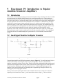
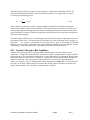
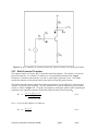
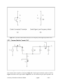
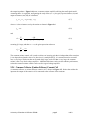
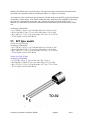
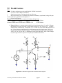
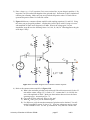
Laboratory Experiment 9 EE348L B.Madhavan Revised by: Aaron Curry University of Southern California. EE348L page1 Lab 9 Table of Contents 9 Experiment #9: Introduction to Bipolar Junction Transistor Amplifiers …………...4 9.1 Introduction ..................................................................................................................................... 4 9.2 Small-Signal Model for the Bipolar Transistor ............................................................................... 4 9.2.1 Canonic Cells used in BJT Amplifiers............................................................................................ 6 9.2.2 Diode-Connected Transistor ............................................................................................................ 7 9.2.3 Common Emitter Canonic Cell ....................................................................................................... 8 9.2.4 Common Collector (Emitter Follower) Canonic Cell ..................................................................... 9 9.2.5 Common Base Canonic Cell.......................................................................................................... 11 9.3 Common Emitter Amplifier Example ........................................................................................... 12 9.4 BJT simulation in HSpice.............................................................................................................. 13 9.5 BJT Spice models.......................................................................................................................... 14 9.5.1 Device Specifications:................................................................................................................... 15 9.6 Conclusion ..................................................................................................................................... 15 9.7 Revision History............................................................................................................................ 15 9.8 References ..................................................................................................................................... 15 9.9 Pre-lab Exercises ........................................................................................................................... 16 9.10 Lab Exercises................................................................................................................................. 18 University of Southern California. EE348L page2 Lab 9 Table of Figures Figure 9-1: Small-signal model for the bipolar transistor. ........................................................................ 4 Figure 9-2: An ac schematic of a common-emitter BJT amplifier canonic cell. Biasing is not shown. ................................................................................................................................ 6 Figure 9-3: (a) Diode-Connected BJT and (b) its low frequency small-signal equivalent circuit. ……..... 7 Figure 9-4: Low frequency small-signal circuit of a common emitter canonic cell. ................................. 7 Figure 9-5: An ac schematic of a common-collector (emitter follower) BJT amplifier canonic cell. Biasing is not shown. ............................................................................................................ 8 Figure 9-6: An ac schematic of a common-base BJT amplifier canonic cell. Biasing is not shown............................................................................................................................................. 9 Figure 9-7: Common-emitter BJT amplifier with emitter degeneration resistance................................. 10 Figure 9-8: Small-signal circuit for common-emitter amplifier with resistive load in Figure 9-8. …….... 10 Figure 9-9: 2N3904 pin out (Courtesy of Fairchild Semiconductor). ...................................................... 12 Figure 9-10: Schematic diagram of the common emitter amplifier for Prelab question 2 ...................... 14 Figure 9-11: Modification of common-emitter amplifier in Figure 9-10 to obtain an emitter-follower for question 5. ................................................................................................... 15 University of Southern California. EE348L page3 Lab 9 9 Experiment #9: Introduction to Bipolar Junction Transistor Amplifiers 9.1 Introduction In the last lab, we learned that an analog circuit has to be biased correctly so that the active devices within the circuit operate in a desirable fashion (linearly) on signals that enter the circuit. These signals are perturbations about the bias point (or quiescent point, a.k.a. Q-point). Ideally, one would like amplifiers to be perfect linear devices, meaning the output signal is some multiple of the input signal, independent of the input amplitude. Since transistors are non-linear devices (recall their I-V characteristics), the output amplitude does depend upon the input amplitude. However, by suitably restricting the amplitude of the input swing (using a “small signal”) and correctly biasing the circuit (Q point), the resultant output will show very little distortion, meaning that the non-linear circuit behaves approximately like a linear circuit for small-signal deviations about the bias point. In this lab, dynamic circuits using BJTs will be introduced. Once a BJT is biased in such a way that it operates in the active region, the “small-signal” BJT model may be used for analysis and design of circuits that contain the transistor. This small-signal model forms the basis for understanding the ac performance of several commonly encountered BJT circuits. 9.2 Small-Signal Model for the Bipolar Transistor Figure 9-1: Small-signal model for the bipolar transistor. The small-signal model for an NPN bipolar transistor is shown in Figure 9-1. The small signal model is just a tool that is used to help circuit designers analyze circuits utilizing BJTs. This tool is only valid if the transistor is operating in its linear or active range. Therefore it should be understood that when using the small signal model, that significant effort has been made to ensure that the signal being processed in the amplifier is not too large, thus validating the “small signal” model accuracy. A large enough signal may cause the transistor to leave its linear operation if its signal change has a magnitude large enough to offset the set Q (biasing) point, thus causing signal distortion. The key element in the small signal model is the controlled current source, which can be shown as depending on the internal base current ib or the internal base-emitter voltage vπ. The internal base- University of Southern California. EE348L page4 Lab 9 emitter voltage is the voltage not including the voltage drop across rb, represented as “vπ” in the small signal model. The quantity gm is defined as gm ic v (9.1) ic I C which is evaluated at the collector bias current IC, signifying how responsive the collector current is to changes in the voltage vπ. The small signal model shown in Figure 9-1 shows the various internal, physical device resistances associated with each terminal of the BJT. Resistor re is the distributed resistance (typically very small in magnitude), associated with the highly doped emitter terminal of the BJT. Resistor rb is a distributed, non-linear resistance, and thus hard to characterize with a single value, but it corresponds to the resistance between the base contact and that region of the base material lying underneath the emitter. Likewise, resistor rc is hard to characterize with a single value, but represents the net resistance between the collector contact and the bottom portion of the base material. Resistor rπ, known as the emitter-base junction diffusion resistance, is not a physical resistance (it is a mathematical model conceived from a Taylor series expansion of the base-emitter current, IBE, about the Q-point) like the preceding three, but rather a dynamic quantity defined as r 1 ib / v (9.2) ib I B which is evaluated at the base bias current IB. It represents how resistant the input base current is to changes in the internal base-emitter voltage (i.e., the voltage not including the voltage drop across rb, represented as “ve” in the small signal model). The controlled source indicates how much the collector current changes for a change in base current (or equivalently, base-emitter voltage). Like rπ, resistor ro is a dynamic resistance and it is known as the forward Early resistance. It represents the influence of changes in collector-emitter voltage on collector current, and thus is calculated by ro 1 ic / vce (9.3) ic I C ,vce VCE For large Early voltages, this resistance is close to infinity, and thus the collector voltage has a negligible impact on the current flowing out of the collector contact. The internal resistance, however, does have profound effects on overall circuit performance. Large base, collector, and emitter resistances (rb, rc, and re) reduce circuit gain, diminish gain-bandwidth product, and increase electrical noise. However, rb, re, and rc are inversely proportional to the emitter-base junction injection area, and a price is paid for increasing the area to lower resistances. Increasing the area of the device results in larger parasitic capacitances. Therefore, increasing the size of the transistor to reduce internal resistance reduces the circuit response speed. Power consumption is also a trade-off. All internal resistance, particularly rb, decrease monotonically with increasing the base and collector bias currents, IB and IC, respectively. In the world of wireless and mobile electronics, we want the batteries in our cell phone to last longer, so large power consumption in wireless electronics is avoided. Welcome to the wonderful world of circuit design, where constraints are inversely proportional to each other. Your job as a circuit designer is to find a happy median that allows you to meet all the specifications for your design. University of Southern California. EE348L page5 Lab 9 The small signal model also accounts for internal parasitic capacitances found within the BJT. Cµ represents the depletion capacitance of the base-collector junction. Cπ is composed of two parts: 1) a diffusion capacitance given by C F ic F gm v (9.4) and 2) a depletion capacitance, which is usually negligible compared to the diffusion capacitance when the base-emitter junction is forward-biased. To develop numerical values for the symbols in the small-signals model, the defining derivatives must be evaluated symbolically, and then evaluated at the Q-point of the BJT in question. With the bias quantities specified, numerical values may be assigned to each small-signal parameter. The small signal model does give a circuit designer a good feel on how parasitic capacitance affects the performance of the circuit. An experienced circuit designer can see the limitations of any topology by inspection. For instance, if bandwidth is being considered, a good circuit designer would avoid exposing any large parasitic capacitance to any large impedances (Remember the time constant, in terms of frequency, is inversely proportional to the product of resistance, R and capacitance, C). 9.2.1 Canonic Cells used in BJT Amplifiers The BJT Transistor has four basic topologies that are building blocks for more complex circuit architecture. A single BJT transistor may be connected in a diode, common-emitter, common- collector (emitter-follower), or common-base configuration. A quick and simple way to determine the difference between the common base, collector, or emitter is: First, determine what terminals where the input and output are connected. Then, the particular canonic cell receives its name from the terminal that is leftover. For example, if you are looking at the ac BJT configuration in Figure 9-2, you will notice that the input is at the base, while the output is located at the collector. Hence, the leftover terminal is the emitter and this canonic cell is deemed a “common emitter” amplifier. University of Southern California. EE348L page6 Lab 9 Figure 9-2: An ac schematic of a common-emitter BJT amplifier canonic cell. Biasing is not shown. 9.2.2 Diode-Connected Transistor The simplest canonic cell for the BJT is the diode-connected transistor. The collector is tied to the base of the transistor, so it exhibits I-V behavior of a conventional PN junction diode. Figure 9-3 depicts a transistor connected this way and its small-signal equivalent circuit. This model assumes the transistor is biased in the linear region and leaves out the Q-point currents. The diode-connected transistor reduces the number of terminals of a typical BJT to two (the base and collector are now the same terminal). This two terminal device may be modeled as a two terminal resistor as shown in Figure 9-3. Using the low-frequency small-signal model of BJT (neglecting all capacitance), the equivalent resistance of the diode-connected can be found to equal Rd. Rd re ro rc || rb r (9.5) ro 1 ro rc rb r If ro >> rc+rb+rπ, then equation 9.5 reduces to Rd re rb r (9.6) 1 University of Southern California. EE348L page7 Lab 9 Figure 9-3: (a) Diode-Connected BJT and (b) its low frequency small-signal equivalent circuit. 9.2.3 Common Emitter Canonic Cell Figure 9-4: Low frequency small-signal circuit of a common emitter canonic cell. The common emitter amplifier was shown in Figure 9-2. Replacing the schematic symbol of a BJT in Figure 9-2 with the small signal model in Figure 9-1, one can calculate the gain, input impedance and University of Southern California. EE348L page8 Lab 9 the output impedance. Figure 9-4 shows a common emitter amplifier utilizing the small signal model. Assuming that rc is negligible, and ignoring the early effect (ro= ∞), the gain, input resistance (rin) and output resistance (rout) may be calculated. rin rb r ( 1)(re rx ) (9.7) where rx is the resistance seen by the emitter as shown in Figure 9-4. rout (9.8) and AV Vo rL Vs rs rb r ( 1)(re rx ) (9.9) assuming β is large, and that rx >> re, the gain expression reduces to AV Vo rL Vs rx (9.10) The common emitter canonic cell is used to achieve an inverting gain that is independent of the transistor β. rin depends on what the value of rx, but since it is multiplied by β, it is assumed not to be too small. rout is very large. With a rin that can be made fairly large, and a rout that is very large, the common emitter is not a very ideal voltage amplifier. Additional transistors can be used to enhance performance, so that the common-emitter canonic can be used as a good voltage amplifier. 9.2.4 Common Collector (Emitter Follower) Canonic Cell A common-collector or emitter-follower canonic cell is shown in Figure 9-5. Notice that neither the input nor the output of the canonic cell is connected to the collector of the transistor. University of Southern California. EE348L page9 Lab 9 Figure 9-5: An ac schematic of a common-collector (emitter follower) BJT amplifier canonic cell. Biasing is not shown. Using the small signal model in Figure 9-1, it can be shown that the gain, input resistance, and the output resistance are the following, assuming that re is negligible compared to rx, AV Vo ( 1)(rx // ro ) Vs rs rb r ( 1)(rx // ro ) (9.11) In this example, assuming that (rs+rb+rπ) is small compared to (1+β)(rx||ro), the gain expression simplifies to AV Vo 1 Vs (9.12) with rin rb r ( 1)(rx ) University of Southern California. EE348L (9.13) page10 Lab 9 and rout rb r ry (9.14) ( 1) Since the gain can be designed nearly equal one, rin can be made fairly large, while rout is small (due to it being inversely proportional to β) the common collector canonic cell can be designed to be a decent voltage buffer. Since the common collector is usually used as a voltage buffer, it is sometimes referred to as an “emitter follower” due to the emitter following (or matching) the voltage that is connected to the base. 9.2.5 Common Base Canonic Cell The common base canonic cell is shown in Figure 9-6. The input is a current source at the emitter, while the output is taken at the collector. Figure 9-6: An ac schematic of a common-base BJT amplifier canonic cell. Biasing is not shown. Using the small-signal model it can be shown that the current gain (Ai), rin, and rout are the following. Ai Io 1 I s ( 1) University of Southern California. EE348L (9.15) page11 Lab 9 rout rin re (9.16) rb r ry (9.17) ( 1) The common base has a current gain of about one, a large output resistance and a small input resistance. Therefore, it is commonly used as a current buffer. 9.3 Common Emitter Amplifier Example In the previous lab, the common-emitter amplifier was biased, but no mention was made of why it is called an amplifier. To answer this, we analyze the common-emitter amplifier circuit in the previous lab, with a few modifications, as shown in Figure 9-7. First, we need to feed our input signal into the base, without the DC bias of the signal source and the common-emitter amplifier interfering with each other. This is accomplished by adding an ac-coupling capacitor (Cc1) to the input port, large enough so that it will act like an AC short at the frequencies at which we operate, thus eliminating any transfer of DC offsets. Since the amplifier needs to drive a resistive load, we insert an ac-coupling capacitor (Cc2) to the output port since we don’t want the load resistor to upset the bias point of the BJT. Figure 9-7: Common-emitter BJT amplifier with emitter degeneration resistance. Third, we replace the transistor symbol used in the previous lab with the small-signal model in Figure 9-1, leading to the following circuit in Figure 9-8. University of Southern California. EE348L page12 Lab 9 Figure 9-8: Small-signal circuit for common-emitter amplifier with resistive load in Figure 9-8. Assuming that we are at low-enough frequencies that the parasitic capacitances of the BJT don’t affect our results, but at a high enough frequency that the coupling capacitors act as a short circuit, and further neglecting the Early effect, resistance of the signal source, the internal base resistance (rb), the internal collector resistance (rc) and the internal emitter resistances (re), the analysis of our model leads to AV vout RL || RC vs r 1Ree (9.18) With large β, this reduces to a rather simple expression independent of transistor parameters. AV RL || RC Ree (9.19) As long as (R L || RC ) > Ree , the transfer function has a magnitude greater than 1, explaining why the common-emitter is called an amplifier. Note that the resistance associated with the input signal source is ignored, which is only valid in an ideal world. This assumption causes the voltage division effects, which would normally be caused by the biasing transistors Rb1 and Rb2, to be ignored. However, if one were to build this circuit, any source resistance would cause these two biasing resistors to diminish the gain and thus would need to be accounted for during design. 9.4 BJT simulation in Spice The syntax (see page 145 of the LTSpice user Manual, or pa ge 20 4 of t he P S pi ce us er ma n ual ) f o r a BJT element in Spice is: qxxx collector base emitter bjt_model_name Where collector, base, emitterare the collector, base, and emitter terminals of the BJT qxxx, and bjt_model_name is the model name of the BJT as specified in the HSpice BJT model deck. The simulation of semiconductor devices requires the specification of an appropriate device model deck in HSpice. The model deck specifies a particular mathematical model of the device being simulated and the values of the parameters associated with the model. Model parameter values that are not specified University of Southern California. EE348L page13 Lab 9 default to the default values specified in Spice. The interested reader can determine the default values associated with a particular model by searching the PSpice or LTSpice user manuals. An example of a Spice model deck specification for 2N3904, the discrete npn BJT used in this laboratory assignment, is shown below. Note that the model deck starts with the keyword .MODEL, followed by the particular n-channel BJT model name, npn_2N3904, followed by the keyword NPN. The “+” character is a continuation character that indicates that the model deck specification continues on that line. .model npn_2N3904 NPN + Is=6.734f Xti=3 Eg=1.11 Vaf=74.03 Bf=416.4 Ne=1.259 Ise=6.734f + Ikf=66.78m Xtb=1.5 Br=.7371 Nc=2 Isc=0 Ikr=0 Rc=1 Cjc=3.638p + Mjc=.3085 Vjc=.75 Fc=.5 Cje=4.493p Mje=.2593 Vje=.75 Tr=239.5n + Tf=301.2p Itf=.4 Vtf=4 Xtf=2 Rb=10 9.5 BJT Spice models *Model for a NPN 2N3904 .model npn_2N3904 NPN + Is=6.734f Xti=3 Eg=1.11 Vaf=74.03 Bf=416.4 Ne=1.259 Ise=6.734f + Ikf=66.78m Xtb=1.5 Br=.7371 Nc=2 Isc=0 Ikr=0 Rc=1 Cjc=3.638p + Mjc=.3085 Vjc=.75 Fc=.5 Cje=4.493p Mje=.2593 Vje=.75 Tr=239.5n + Tf=301.2p Itf=.4 Vtf=4 Xtf=2 Rb=10 *Model for a PNP 2N3906 .model pnp_2N3906 PNP + Is=1.41f Xti=3 Eg=1.11 Vaf=18.7 Bf=180.7 Ne=1.5 Ise=0 + Ikf=80m Xtb=1.5 Br=4.977 Nc=2 Isc=0 Ikr=0 Rc=2.5 Cjc=9.728p + Mjc=.5776 Vjc=.75 Fc=.5 Cje=8.063p Mje=.3677 Vje=.75 Tr=33.42n + Tf=179.3p Itf=.4 Vtf=4 Xtf=6 Rb=10 Figure 9-9: 2N3904 pin out (Courtesy of Fairchild Semiconductor). University of Southern California. EE348L page14 Lab 9 9.5.1 Device Specifications: Caution: Never exceed the device maximum specifications during design. 2N3904 VCBmax=60V VCEmax=40V VEBmax=5.0V ICmax=200mA 2N3906 VCBmax=40V VCEmax=40V VEBmax=5.0V ICmax=200mA 9.6 Conclusion The use of the BJT as an amplifier was explored in this experiment. There were four fundamental configurations covered that are known as the BJT canonical cells. Each canonic cell has unique beneficial characteristics as well as limitations. It is very crucial that the canonic cells are well understood, as they will give a circuit designer the ability to evaluate complex circuit topologies virtually by inspection. 9.7 Revision History This laboratory experiment is a modified version of the laboratory assignment 9 (BJT Dynamic Operation) created by Jonathan Roderick, Hakan Durmas, and Scott Kilpatrick Burgess. 9.8 References [1] Bindu Madhavan, Laboratory Experiment 5 biasing supplement, EE348L, Spring 2005 [2] PSpice User Manual, posted on EE348L class web site. [3] LTSpice User Manual, posted on EE348L class web site. [4] Bindu Madhavan, EE348L Laboratory Experiment 3, Spring 2005. [5] Adel Sedra and K. C. Smith, Microelectronic Circuits, fifth edition, Oxford University Press. [6] David Johns & Ken Martin. Analog integrated Circuit Design. John Wiley & Sons, Inc., New York, 1997. [7] Paul R. Gray & Robert G. Meyer. Analysis and Design of Analog Integrated Circuits. John Wiley & Sons, Inc., New York, 1993. University of Southern California. EE348L page15 Lab 9 9.9 Pre-lab Exercises Note: • For Spice simulations, use the model deck for 2N3904 in section 9.4. • Let Cc be 10 uF for HSpice simulations. • Submit plots relevant to each question in your lab report. • Review the biasing of a CE amplifier as discussed in laboratory experiment 8, along with your answer to laboratory experiment 8, lab question 5. • Device Specifications: Caution: Never exceed the device maximum limitations during design. 2N3904 VCBmax=60V VCEmax=40V VEBmax=5.0V ICmax=200mA 2N3906 VCBmax=40V VCEmax=40V PVEBmax=5.0V ICmax=200mA 1) Figure 9-10 shows a common emitter amplifier with coupling capacitors Cc1 and Cc2. Design this amplifier for a gain of 10 with 2.5mA of drain current, Vcc=10V, and Vce=5V. Let Rl be infinitely large in your design. Assume that Vs is a 10 kHz sine wave input with amplitude of 50 mV. Be sure that your signal doesn’t drive the transistor out of the linear region. Verify your design using a transient simulation in Spice. In your simulations sweep Rl over the following values: 1e9, 10k, 1k, 100, and 50. What happens to the gain as Rl drops? Why? Make changes to your design to achieve a gain of 10 in your Spice simulation for Rl=1e9. Figure 9-10: Schematic diagram of the common emitter amplifier. University of Southern California. EE348L page16 Lab 9 2) Place a large (e.g., 0.1 µF) capacitor (Cee) across resistor Ree in your design in problem 1. By inspection, can you reason what happens to the gain and why? Perform an ac Spice simulation to confirm your reasoning. Make sure your sweep includes frequencies where Cee looks like an open and frequencies where Cee looks like a short. 3) Figure 9-11 shows a common collector amplifier with coupling capacitors Cc1 and Cc2. Using the values you got for prelab problem 1, simulate this circuit in Spice with Vs being a sin wave with amplitude of 50mV and a frequency of 10kHz. What is the voltage gain? In your simulations sweep Rl over the following values: 1e9, 10k, 1k, 100, 50. What happens to the gain as Rl drops? Why? Figure 9-11: Schematic diagram of the common collector amplifier. 4) Refer to the common emitter amplifier in Figure 9-10. A) What is the maximum gain that can be achieved if the collector current is fixed at 2.5 mA and the emitter voltage, VE, is fixed at .3V? Assume that Vs is a 10 kHz sine wave with amplitude of 50mV. Make sure the transistor does not leave the linear operating region. Assume that Vbe~.7V. B) Can a gain of 50 be achieved? Why or why not? C) What RC value gives you the maximum gain? D) Use HSpice to verify the maximum amount of gain that can be obtained. You will need to sweep Rb2 to ensure Ve sits at .3V. Your base voltage may not be exactly 1V but it should be close. Use the .op command to verify the bias currents and University of Southern California. EE348L page17 Lab 9 voltages for your circuit, and a .tran analysis to observe the voltage gain. Plot Vc and Vb. Does Vc ever drop below Vb? If it does, find a new Rc so that it does not. Hint: The maximum the base voltage will be is Vb(bias)+Amplitude(Vin). The minimum the collector voltage will be is: Vc(bias)-Av*Amplitude(Vin). University of Southern California. EE348L page18 Lab 9 9.10 Lab Exercises • Submit plots relevant to reach question in your lab report. • Use the supply voltage that you used in your Pre-lab Spice simulations for this lab. • Ensure that the device is oriented correctly before using it in your circuit. • For proper operation, the base-emitter junction has to be forward biased and the collector-base junction has to be reverse biased. • Remember that an amplitude of 50mV corresponds to a Vpp of 100mV. 1) Build the circuit you designed for Pre-lab question 1 with an open load. Measure the gain and the current through each branch and compare it to your Spice results. Are your results within 5% of specifications given in the Pre-lab? Perform any necessary changes or tweaking of resistor values to get within 5% of specs. Next, change the input signal amplitudes to 100mV, 200mV, and 300mV. Does the circuit still behave linearly? Why or why not? 2) Now, add a load to your circuit in exercise 1. Vary the load from 10k, 1k, 100, and 50. What happens to the gain? Do your results agree with your pre-lab Spice simulations from pre-lab problem 1? 3) Place a large (e.g., 0.1 µF) capacitor across resistor Ree of exercise 1. Using a function generator, sweep the frequency from 1 kHz to 36 kHz taking a measurement of the magnitude every 5 kHz (eight data points). What does adding the capacitor do to the gain? Does this agree with your prediction for Pre-lab question 3? 4) Using the common-emitter amplifier you used in question 1, change it to an emitter-follower amplifier by taking the output at the emitter as shown in Figure 9-11. What is the gain of this circuit? 5) Now, add a load resistance, RL to the emitter follower and measure the gain for Rl=10k, 1k, 100, and 50. Does driving a small load resistance affect the ac gain of you circuit? Why is this circuit beneficial? Could you drive the same small load resistance with a common-emitter? Why or why not? 6) Build the design which gives you the maximum achievable gain, but replace RC in Figure 9-10 with a potentiometer. Vary the potentiometer until you reach the maximum achievable gain while still maintaining a collector-base reverse bias to ensure linearity. ( D o t h i s b y probing the collector and base voltages and make sure the collector voltage n e v e r d r o p s b e l o w t h e b a s e v o l t a g e . ) Measure the value of the potentiometer that gives you the maximum possible gain. Does this value agree with what you derived in Pre-lab question 2? Why or why not? University of Southern California. EE348L page19 Lab 9