1
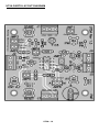
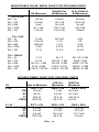
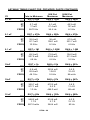
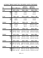
INTRODUCTION The UT5A is most versatile 555 timer kit on the market. The input circuit options allow for connecting to almost any kind of digital signal. The output drivers allow for connection to digital circuits, relays, indictors, etc... It is designed to provide the easiest way to apply accurate timing signals to almost any application. The UT5A is also an excellent teaching tool. The detailed theory of operation will arm you with the knowledge to effectively set up and use the 555 timer. You will have the chance to experiment with the 555 timer IC, transistor switches, pull-up resistors, limiter, and differentiator circuits. In addition, experienced 555 IC users will welcome the practical and truly universal setup of the PC board. THEORY OF OPERATION Theory Intro: The UT5A is made up of many small circuits used to control the 555 timer IC, which is the heart of the kit. First we’ll cover these circuits individually, then we’ll place them into the two most basic modes of operation (monostable and astable) and analyze their operation. Power Entry: The UT5A requires an external 5 to 15 VDC DC power supply to operate the timer circuits. This external DC supply is connected through J1, positive at pin 1 and negative (GND) at pin 2. J1 pin 3 allows for a separate 3 to 24 VDC supply to be used to set the output signal amplitude parameters or Output Power. JMP1 allows the Timer Power to be used for Output Power. Input Circuits: Triggering the 555 timer IC requires a negative going signal applied to its input. We have three ways to apply this signal to the IC. 1) NEGATIVE INPUT - If the source signal is negative going it can be applied to J2 pin3 the boards (-) Input which is attached to C1. For this option JMP2 (Pull-up Select) may or may not be installed depending on the source. If installed, it supplies VCC through R1 to C1’s input. J2 pin3 allows us to bring a negative signal into the timer at C1. With a negative input, D1 is turned off, thus preventing Q1 from effecting the input signal. 2) POSITIVE INPUT - This option requires JMP2 (the Pull-up Select) to be installed to provide power for Q1. The positive pulse enters through J2 pin 1 (+ Input) current limiting resistor R2 to the base of Q1. The positive signal turns on Q1. It amplifies and inverts the signal, and now we have a negative going pulse passed by the steering diode D1 to C1’s input. UT5A 4 3) START SWITCH INPUT - We can also generate a negative signal using Start switch S1. This final option also requires JMP2 (Pull-Up Select) to be installed. Pull-up resistor R1 keeps a High (+VCC) at S1/C1 junction with no input signal applied to J2 pin3. When S1 is pressed it pulls S1/C1 junction low, giving us a negative pulse at C1’s input. Differentiator Circuit and Limiter: If the input pulse has a long negative duration, it can override the 555 timer’s output. In most cases this is not desirable, however if it is then you can install JMP3 (Differentiator Select). When JMP3 is not installed, C1 and R3 act as a differentiator circuit. This circuit will turn an input square wave or long duration pulse into a negative and positive short duration pulse. Pulse width is determined by C1’s charge or discharge path. Since R3 is tied to VCC the junction of C1/R3 will rest at VCC. The short duration pulses will be imposed on that DC level. The negative short duration pulse will have an amplitude slightly less than the original pulse. The positive short duration pulse will have its amplitude limited by D2 to a maximum of VCC + 0.7V. This is to prevent false operation of the timer IC. JMP2 (Input Select) must be installed for any circuit requiring an external trigger input. Charging Network: R4, R5, R6, R7, and C2 make up the RC network responsible for all timing in the UT5A. The component values determine the rate at which the capacitor (C2) charges and discharges. JMP6 controls the way the charging network is connected to the timer IC. JMP6 also determines the mode of operation, which we will discuss later. Timer Pin-out and Function: The 555 timer IC has 8 pins. Pin1 provides Ground to all timer functions. Pin8 is +VCC and provides power for all IC functions. Pin3 is the Output pin; it will be either High (near +VCC) or a Low (near 0 VDC) depending on the status of the input pins. Pin7 is called Discharge, it will provide ground to the charging network when the Output (Pin3) is Low and an open when the Output is High. Pin2 is the Trigger input. When the voltage on this pin falls below the trigger level (usually 1/3 VCC) it will cause the Output (Pin3) to go High and remove the ground from Discharge (Pin7). UT5A 5 Pin6 is called the Threshold input. When the voltage on this pin rises above the Threshold Level (usually 2/3 VCC) it cause, the Output to go Low and place, a ground in the charging network through the Discharge (Pin7). Pin4 is the Reset. When this pin goes low it will override the other inputs and force the Output to go Low and the Discharge to provide a ground to the charging network. Pin5 is the Control Voltage. This pin allows the Trigger and Threshold levels to be independent of VCC. When this pin is connected the Threshold level will be equal to the Control Voltage pin (J3 pin1) and the Trigger level will be ½ Control Voltage pin. Reset Circuit: The Reset circuit consists of R11, C6, J3 pin3 (Reset Input) S2 and U1 pin4. R11 is a pull-up resistor that keeps the timer’s RESET pin normally High. C6 is a filter capacitor to ensure that noise doesn’t accidently reset the timer IC. S2 is a normally open push button switch that when closed pulls U3 pin4 low, resetting the timer IC. J3 allows for an external reset of the timer IC. Control Voltage Circuit: The control voltage circuit is used to change the trigger levels of the timer as mentioned in Timer Pin-out and Function. It also can be used for pulse width and pulse position modulation. C4 is a filter capacitor that ensures noise does not effect timer operation. R8 allows the Control Voltage to be set to any value between 0 and +VCC. JMP5 allows R8’s wiper voltage to be applied to the timer IC. J3 pin1 allows for an external Control Voltage. This voltage can be any voltage up to +VCC AC or DC. JMP5 should not be installed if an external Control Voltage is being used. With JMP5 removed and no input on J3 pin1, the 555 timers Trigger and Threshold voltages are at their default 1/3 VCC and 2/3 VCC values respectively. Timer Output Circuits: The Inverted Timer Output circuit consists of current limiting resistor R9, pullup resistor R10, protection diode D3, and transistor Q2. The Non-inverted Timer Output consists of JMP7 the Non-Invert jumper, R12 pull-up resistor, protection diode D4, and transistor Q3. The output of the timer chip U1 pin3 is connected to Q2 through current limiting resistor R9. If U1’s pin3 output is Low the base of Q2 is Low, which turns it off. This allows pull-up resistor R10 to pull Q2’s collector High. If JMP7 is removed this High (approximately +V) is applied to J5 pin2 as the Inverted Timer Output. If JMP7 is installed this high (approximately +0.7VDC) is applied to the base of Q3. This causes Q3 to turn on pulling, its collector UT5A 6 low (approximately 0VDC). The Low appears at J4 pin 1 as the Non-inverted Timer Output. If U1’s pin3 output is High, the base of Q2 is High, causing it to be turned on. This pulls Q2’s collector Low, and this Low (approximately 0VDC) is applied to J5 pin2 as the Inverted Timer Output. If JMP7 is installed, this Low (approximately 0VDC) is applied to the base of Q3, turning it off. This allows pull-up resistor R12 to pull Q3’s collector High (approximately +V). The High appears at J4 pin 1 as the Non-inverted Timer Output. The Inverted Timer Output at J5 pin2 and Non-Inverted Timer Output at J4 pin1 can be used as logic level outputs. A Low is less than 200mV and a High is from +3 to +24V, depending on the supply voltage used for V+. They also can be used to drive a load of up to 200mA if the load is connected between +V pin at J4 pin2 and either of the Timer Output pins. To have the load active when the timer’s output at U1 pin3 is High, connect the load between J4 pin2 and J5 pin2. To have the load active when the timer’s output at U1 pin3 is Low connect the load between J4 pin2 and J4 pin1. D3 and D4 protect Q2 and Q3 respectively from inductive kick if an inductive load is used. MODES OF OPERATION Note: For these explanations we will assume no Control Voltage input. Only basic operation is covered here. Monostabe Mode: In Monostable mode the timer acts as a “one shot” pulse generator. It has one Stable and one Unstable state. The pulse begins with a negative input trigger. This causes the output of the 555 timer to go from low to high starting the pulse (Unstable). The Pulse Width is determined by the charging network’s RC time constant. When the circuit times out the output of the 555 timer goes from high to low completing the pulse (Stable). The timer will remain in this Stable state until it is triggered again. In Monostable mode the 555 timer requires an external negative pulse or spike to start its operation. We will be using the pulse provided by the Input, Differentiator, and Limiter circuit previously described. This means JMP4 (Input Select) must be installed. JMP6 (Mode Select) set to pins 1 and 2 prepares the Charging Network for Monostable operation. The C2’s charge path can be traced by starting at +VCC down through R4, R5, to the pin7 (Discharge) of the timer IC, through JMP6 pin1 to pin2, to C2. You may notice that R6 and R7 are bypassed in this mode. C2 is also directly connected to pin6 (Threshold) of the timer IC. When C2 is charging the Monostable is in its Unstable state. C2 is allowed to charge when U1 pin3 (Output) is High and pin7 (Discharge) is providing an UT5A 7 open. The Monostable mode’s Stable State is defined as U1’s Output at pin3 is Low and its Discharge pin at U1 pin 7 is held at ground allowing C2 to discharge or preventing it from charging. The timer will stay in this mode until properly triggered. The discharge path will be from C2 through JMP6 pin2 to pin 1, U1 pin7, to ground through the 555 timer IC, back to C2. When the proper trigger appears at U1 pin2 (Trigger) input the Output at pin3 goes High and the ground at pin7 is removed (unstable state). This allows C2 to start to charge through JMP6 pins 1 to 2, R5, and R4 to VCC. When the charge on C2 reaches the Threshold level (2/3 VCC or Control Voltage if used) U1 pin6 (Threshold) will cause the 555 timer to change to the stable state setting the Output pin (pin3) to a Low and applying ground at the Discharge pin (pin7). The Discharge pin (pin7) being at ground discharges C2. The time C2 charges in the Unstable state is the Pulse Width (PW) of the signal, it can be calculated with the following formula. C2’s discharge path has no resistance so it is considered to be instantaneous. It is important to note that the use of a control voltage will change the Threshold level of the IC; therefore, change the RC timing and the pulse width. PW = 1.1 * C2 * (R4 +R5) Astable Mode: In the Astable (no stable states) mode the timer is free running and acts like a square wave generator. We will call the High output of the square wave from the 555 timer Pulse Width (PW) and the Low portion of the square wave Rest Time (RT). The Pulse width is determined by the RC charge time of the Charging Network and Rest Time is determined by the discharge time of the Charging Network. In Astable mode JMP4 (Input Select) is removed disconnecting the signal inputs. JMP6 is set connecting pin2 and pin3. This sets up C2 charge and discharge path and connect both U1 pin2 and pin6 to C2. Since this mode is free running no input, other than applying power, is needed to start the circuit. Lets start at the end of rest time with U1 pin3 (Output) Low, U1 pin7 (Discharge) grounded, and C2 discharging slowly. When the charge on C2 decreases below the Trigger level (1/3VCC or ½ control voltage if used) U1 pin2 (Trigger input) causes the start of Pulse Width by setting U1 pin3 (Out) to go High and Discharge (pin7) removes ground. C2 is now allowed to charge through R7, R6, R5, R4, to VCC. When C2’s charge reaches Threshold level (2/3 VCC or Control Voltage if used) U1 pin6 (Threshold) ends UT5A 8 Pulse Width and begins Rest Time by setting Out to Low and grounding Discharge. C2 now discharges through R7, R6, U1 pin7, to ground in the 555 timer, back to C2. When C2 reaches Trigger level Rest Time comes to an end and we begin the process over again. Formulas for calculating Pulse Width (PW) and Rest Time (RT) follow (assuming no control Voltage used): PW = 0.693 * C2 * (R4 + R5 + R6 + R7) RT = 0.693 * C2 * (R6 + R7) Total Time (T) can be calculated as: T = PW +RT Or T = 0.693 * C2 * [(R4 + R5) + 2(R6 + R7)] Frequency (f) can be calculated as: f = 1 T = 1 _ 0.693 * C2 * [(R4 + R5) + 2(R6 + R7)] Duty cycle is the ratio of Pulse Width to Total Cycle time, it can be calculated as: R4 + R5 + R6 + R7 DC = R4 + R5 + 2(R6 + R7) * 100% UT5A 9 UT5A PARTS LAYOUT DIAGRAM UT5A 10 UT5A PARTS LIST Semiconductors 1 555 Timer IC (marked 555) U1) 2 1N4002 (marked 1N4002) (D3,4) 2 1N4148 (marked 1N4148) (D1,2) 3 2N3904 NPN General Purpose transistors (marked 2N3904) (Q1,2,3) Resistors 4 1k ohm resistors (marked brown-black-red) (R2,5,7,9) 5 10k ohm resistors (marked brown-black-orange) (R1,3,10,11,12) 2 47k ohm resistors (marked Yellow-violet-orange) (R5A,7A) 2 82k ohm resistors (marked grey-red-orange) (R5B,7B) 2 470k ohm resistors (marked yellow-violet-yellow) (R5C,7C) 2 1M ohm resistors (marked brown-black-green) (R5D,7D) 2 50k potentiometer (orange top marked 503) (R4A,6A) 1 100k potentiometer (orange top marked 104) (R8) 2 500k potentiometer (orange top marked 504) (R4,6) Capacitors 3 0.01uF Ceramic disk (marked 103) (C1,4,6) 1 0.01uF Ceramic disk (marked 104) (C5) 1 0.1uF Mylar (marked 104) (C2A) 2 10uF Electrolytic marked (marked 10uF) (C2,3) 1 1000uF Electrolytic marked (marked 1000uF) (C2B) Connectors 2 Two terminal, terminal block (J4,5) 3 Three terminal, terminal block (J1,2,3) 6 2 pin header (H1,2,3,4,5,7) 1 3 pin header (H6) 7 Jumper Blocks Other 2 SPST Push Button switch (S1,2) 1 Circuit Board UT5A 11 tors have no polarity so they can be installed in either direction. 6. Install C5, a 0.1uF ceramic capacitor (marked 104). 7. Install C4, another 0.01uF ceramic capacitor (marked 103). 8. Install C6, the last 0.01uF ceramic capacitor (marked 103). 9. Install Q1, the transistor marked 2N3904. this part must be mounted in a specific direction. Match the shape of the transistor to the outline shown on the parts location diagram or the silkscreen on the circuit board. Mount it as close to the board as possible 10. Install Q3, another 2N3904 transistor. Follow the same care of installation as you did with Q1. 11. Install Q2, the last 2N3904 transistor. 12. Install R1, a 10k ohm resistor (marked brown-black-orange). Resistors are like ceramic capacitors they have no polarity. They can be installed in either direction. All resistors in this kit are stand up resistors. The pad with the silkscreen circle is the pad that the body of the part sits on. 13. Install R3, another 10k ohm resistor (marked brown-black-orange). 14. Install R12, yet another 10k ohm resistor (marked brown-blackorange). 15. Install R10, still another 10k ohm resistor (marked brown-blackorange). 16. Install R9, a 1k ohm resistor (marked brown-black-red). 17. Install R11, the last 10k ohm resistor (marked brown-black-orange). 18. Install R2, a 1k ohm resistor (marked brown-black-red). 19. Install R8, a 100k ohm variable resistor (marked 104). This part has three legs and will only fit easily in one direction. 20. Install S1, a SPST Push Button switch. This part will fit in the board in two different directions, either one will work. 21. Install S2, an other SPST Push Button switch. 22. Install JMP2, a 2 pin header. 23. Install JMP3, another2 pin header. 24. Install JMP4, another2 pin header. UT5A 16 25. Install JMP1, another2 pin header. 26. Install JMP7, you guessed it another 2 pin header. 27. Install JMP6, a 3 pin header. 28. Install JMP5, finally the last 2 pin header. 28. Install D4, this diode is marked 1N4002. This part has a black body with one silver or white stripe on one end. It is a stand up diode. Bend the lead closest to the stripe over so that it comes back across the diode and is in parallel with the other lead. Match this (stripe end) lead to the circuit board pad closest to the white stripe on the board’s silkscreen. The lead attached to the black body goes through the hole with the silkscreen circle. 30. Install D3, another 1N4002 diode (marked 1N4002). Install this diode in the same manor as D4. 31. Install C3, a 10uF electrolytic capacitor (marked 10uF). Electrolytic capacitors have a right and wrong way to be installed. Usually, these capacitors have a wide stripe which indicates their polarity. Most of the time this stripe indicates the negative lead. This can be verified by looking for the (-) sign in the stripe. On rare occasions this stripe with have a (+) sign indicating a positive polarity. The PC board or Parts Layout Diagram will show the positive side of the capacitor's installation hole. Be sure to place the ( + ) capacitor lead into the PC board ( + ) hole and the ( - ) lead into the ( - ) hole. Observe correct polarity when installing all electrolytic capacitors. 32. Install J2, a three terminal-terminal block. The wire openings must face outboard. Make sure the terminal block is square and flush to the circuit board. 33. Install J1, another three terminal-terminal block. Install it with the same precautions you did J2. 34. Install J4, a three terminal-terminal block. 35. Install J5, a three terminal-terminal block. 36. Install J3, the last three terminal-terminal block. You will probably notice five parts are still missing from your board and you have more than five parts left. A this point you will need to figure out what part values you need to install for your first application. See the theory of operation section for calculations or the charts that follow at the end of this section for a component values. UT5A 17 Two different values potentiometers are provided to allow for better tuning of your timer. The 50k pot allows for fine tuning when more precise pulse widths are required. The 500k pot allows for greater time ranges. The Monostable Pulse Width chart shows the Pulse Widths available with provided components. The R4 Minimum column shows the minimum (0 ohms) Pulse Width for both provided potentiometers (50K and 500K) and the capacitor resistor combination shown in the left most column. The R4 = 50k/R4 Maximum column shows the maximum Pulse Width of the 50k pot and the resistor capacitor combination shown in the left most column. The R4 = 500k/R4 Maximum column does the same for R4= 500k. The Astable Timing Chart works the same way as the Monostable Pulse Width chart in addition to Pulse Width it also provides Rest Time, Total Time, and Frequency. This chart it assumes that R4 = R6 and R5 = R7 which is not required. You may mix and match the potentiometers and resistors as you wish. 37. Install R4, either the 50k (marked 503) or 500k (marked 504) potentiometer. Make sure this part is square and flush to the board. 38. Install R6, the other timing potentiometer either the 50k (marked 503) or 500k (marked 504). 39. Install R5, using the calculations or charts select your part value. Used the parts list description of color bands (Example 1K marked brownblack-red) to select the proper resistor. 40. Install R7, for this part follow the instructions for R5 above. 41. Install C2, using the calculations or charts select your part value. If you select the 0.1uF capacitor (marked 104) polarity is no concern. If you select the 10uF (marked 10uF) or the 1000uF (marked 1000uF) electrolytic capacitor observe correct polarity. UT5A 18 MONOSTABLE PULSE WIDTH CHART FOR PROVIDED PARTS R4 Minimum R4=50k Pot R4 Maximum R 4= 500k Pot R4 Maximum C2 = 0.1uF R4 = 1k R4 = 47k R4 = 82k R4 = 470k R4 = 1M 110 uS 5.2 mS 9 mS 51.7 mS 110 mS 5.6 mS 10.7 mS 14.5 mS 106.7 mS 115.5 mS 55.1mS 60.2 mS 64 mS 106.7mS 165mS C2 = 10uF R4 = 1k R4 = 47k R4 = 82k R4 = 470k R4 = 1M 11 mS 517 mS 902 mS 5.2S 11 S 561 mS 1.1 S 1.5 S 5.72 S 11.6 S 5.5S 6S 6.4S 10.7S 16.5 S C2 = 1000uF R4 = 1k R4 = 47k R4 = 82k R4 = 470k R4 = 1M 1.1 S 51.7S 90.2 S / 1.5M 517S / 8.6M 1100 S / 18.3 M 56.1 S 106.7S / 1.8M 145.2S / 2.4M 572 S / 9.5 M 1155 S / 19.3 M 551.1S / 9.2M 602S / 10M 640S / 10.7M 1067S / 17.8M 1650S / 27.5M ASTABLE TIMING CHART FOR PROVIDED PARTS C2 0.1uF Pots to Minimum R5/7 = 1k 139 uS PW 50K Pot Maximum R4/6 = 51k 7.1 mS RT TT FREQ 69 uS 208 uS 4810 Hz 3.5 mS 10.6 uS 94.3 Hz PW RT TT FREQ R5/7 = 47k 6.5 mS 3.3 mS 9.8 mS 102.3 Hz R4/6 = 97k 13.4 mS 6.7 mS 20.2 mS 49.6 Hz 0.1 uF UT5A 19 500K Pot Maximum R4/6 = 501k 69.4 mS 34.7 mS 104.2m S 9.6 Hz R4/6 = 547k 75.8 mS 37.9 mS 113.7 mS 8.8 Hz ASTABLE TIMING CHART FOR PROVIDED PARTS CONTINUED C2 0.1 uF 50K Pot Maximum R4/6 = 132k 18.3 mS 9.1 mS 27.4 mS 36.4 Hz 500K Pot Maximum R4/6 = 582k 80.7 mS 40.3 mS 121 mS 8.3 Hz PW RT TT FREQ R5/7 = 470k 65.1 mS 32.6 mS 97.7 mS 10.2 Hz R4/6 = 520k 72.1 mS 36 mS 108.1 mS 9.3 Hz R4/6 = 970k 134.4 mS 67.2 mS 201.7 mS 4.9 Hz PW RT TT FREQ R5/7 = 1M 138.6 mS 69.3 mS 207.9 mS 4.8 Hz R4/6 = 1.05M 145.5 mS 72.8 mS 218.9 mS 4.6 Hz R4/6 = 1.5M 207.9 mS 104.0 mS 311.9 mS 3.2 Hz PW RT TT FREQ R5/7 = 1k 13.9 mS 6.9 mS 20.8 mS 48.1 Hz R4/6 = 51k 706.9 mS 353.4 mS 1.06 S 0.9 Hz R4/6 = 501k 6.9 S 3.5 S 10.4 S 96 mHz PW RT TT FREQ R5/7 = 47k 651.4 mS 325.7 mS 977.1 mS 1.0 Hz R4/6 = 97k 1.3 S 672.2 mS 2.0 S 496.0 mH R4/6 = 547k 7.6 S 3.8 S 11.4 S 88 mH PW RT TT FREQ R5/7 = 82k 1.1 S 568.2 mS 1.7 S 587.0 mHz R4/6 = 132k 1.8 S 914.8 mS 2.7 S 364.4 mS R4/6 = 582k 8.1 S 4.0 S 12.1 S 83 Hz Pots to Minimum R5/7 = 82k 11.4 mS PW 5.7 mS RT 17 mS TT 58.70 Hz FREQ 0.1 uF 0.1 uF 10uF 10uF 10 uF UT5A 20 ASTABLE TIMING CHART FOR PROVIDED PARTS CONTINUED Pots to Minimum 50K Pot Maximum PW RT TT R5/7 = 470k 6.5 S 3.3 S 9.8 S R4/6 = 520k 7.2 S 3.6 S 10.8 S R4/6 = 970k 13.4 S 6.7 S 20.2 S PW RT TT R5/7 = 1M 13.9 S 6.9 S 20.8 S R4/6 = 1.05M 14.6 S 7.3 S 21.8 S R4/6 = 1.5M 20.8 S 10.4 S 31.2 S PW RT TT R5/7 = 1k 1.4 S 693 mS 2.1 S R4/6 = 51k 70.7 S 35.3 S 106 S R4/6 = 501k 694.4 S / 11.6 M 347.2 S / 5.8M 1041.6 S/ 17.4 M PW RT TT R5/7 = 47k 65.1 S / 1 M 32.6 S / .54 M 97.7 S / 1.6 M R4/6 = 97k 134.4S / 2.2M 67.2 S / 1.1 M 201.7 S / 3.4M R4/6 = 547k 758.1 S / 13.6 M 379.1 S / 6.3 M 1137.2 S / 19.0 M C2 10uF 10 uF 1000uF 1000uF 500K Pot Maximum 1000uF R5/7 = 82k PW 113.7 S / 1.9 M RT 56.8 S / 1.0 M TT 170.5 S / 2.8 M R4/6 = 132k R4/6 = 582k 183 S / 3.1 M 806.7 S / 13.4 M 91.5 S / 1.5 M 403.3 S / 6.7 M 274.4 S / 4.6 M 1210.0 S / 20.2 M 1000uF R5/7 = 470k R4/6 = 520k R4/6 = 970k PW 651.4 S / 10.9 M 720.7 S / 12.0 M 1344.4 S / 22.4 M 360.6 S / 6.0 M 672.2 S / 11.2 M RT 325.7 S / 5.4 M TT 977.1 S / 16.3 M 1081.1 S / 18.0 M 2016.6 S / 33.6 M 1000uF R5/7 = 1M R4/6 = 1.05M R4/6 = 1.5M PW 1386.0 S / 23.1 M 1455.3 S / 24.3 M 2079.0 S / 34.7 M RT 693.0 S / 11.6 M 727.7 S / 12.1 M 1039.5 S / 17.3 M TT 2079 S / 34.7 M 2183.0 S / 36.4 M 3118.5 S / 52. M UT5A 21 SETUP Monostable Mode: 1. Install a Shorting Block across pins 1 & 2 of JMP6. 2. In the Monostable mode the timer needs an input. Install a Shorting Block across both pins of JMP4. 3. Connect the source circuit to J2. Connect the input to J2 pin 1 if the signal is a positive going pulse or pin 3 if it is a negative going pulse. Connect the ground of the source circuit to J2 pin 2. If the input signal is a square wave or a wide pulse you can select which edge of the waveform you wish the timer to trigger. If you wish to trigger on the positive going transition connect to pin 1 if the negative going transition connect to pin 3. 4. Your input circuit may need a pull-up resistor. If the source circuit provides both a high and low the pull-up will not be needed so remove the Shorting Block from JMP2. If the input circuit provides a contact closure or open/closed path for current then you will need the pull-up resistor. Place a Shorting Block on the pins of JMP2. 5. If the input signal is a square wave or wide duration pulse you will probably need the signal to be differentiated. This prevent the input signal from interfering with the timing of the timer. Remove the Shorting Block from the pins of JMP3 to activate the differentiator circuit. If it is required that the differentiator be disabled install a Shorting Block across JMP3’s pins. This Shorting Block will normally not be installed 6. Verify that R4, R5, and C2 are the proper values to give the timing you require. Astable Mode: 1. Install a Shorting block across pins 2 & 3 of JMP6. 2. Typically a in the Astable mode an input is not required. Remove the Shorting Block from JMP4. This removes R3 and R1 from C2’s charge path with JMP6 jumped pins 2 to 3. 3. Verify that R4, R5, R6, R7 and C2 are the proper values to give the timing you require for both Pulse Width and Rest Time. Control Voltage Configuration: 1. For no Control Voltage remove the Shorting Block from JMP5 and leave J3 pin 1 open. UT5A 22 2. For an External Control Voltage remove the Shorting Block from JMP5. Connect an external supplies (0 to VCC) positive lead to J3 pin 1 and its negative lead to J3 pin 2. 3. To use onboard Control Voltage Adjust install a shorting block across both pins of JMP5. Reset Mode: 1. For External Reset connect a momentary closed switch between J3 pins 2 and 3. 2. For Onboard Reset Leave J3 pin 3 open and press S2. Output Connections: 1. For a digital Non-inverted signal install a Shorting Block across both pins of JMP7. Connect J4 pin 1 to the load circuits signal input. Connect J5 pin 1 to the load circuits ground. 2. For a digital Inverted signal remove the Shorting Block from JMP7. Connect J5 pin 2 to the load circuits signal input. Connect J5 pin 1 to the load circuits ground. 3. To connect a load such as a relay or lamp so that the load is energized when the output of the timer is high remove the Shorting Block from JMP7. Connect the positive lead (if applicable) of the load to J5 pin 2. Connect the negative lead (if applicable) of the load to J5 pin 1. 4. To connect a load such as a relay or lamp so that the load is energized when the output of the timer is low install a Shorting Block across both pins of JMP7. Connect the positive lead (if applicable) of the load to J4 pin 1. Connect the negative lead (if applicable) of the load to J5 pin 1. Power Connections: 1. Connect a power sources (5 to 15 volts DC) positive lead to J1 pin 1 and its negative lead to J1 pin 2. 2. It is time to decide if you are going to use Timer Power or a separate power supply (3 to 24 volts DC) to power the Timer Output Circuits. To use Timer Power install a Shorting Block across the pins of JMP1. If you are going to use a separate supply remove the Shorting Block at JMP1. Connect your separate supplies positive lead to J1 pin 3 and the negative lead to J1 pin 2. UT5A 23 TROUBLESHOOTING The most common reason for a hobby kit to fail is improper installation of parts. Approximately 95% of the kits that come back to the factory for repair have improperly installed components, even after phone or email support has recommended reviewing the kit for these problems. We have thousands of examples that prove that even those with vast electronic experience can make mistakes on a simple kit! So before you reach for the phone, please recheck your kit for the following: Proper Parts Placement Proper Parts Orientation Solder Bridges Incomplete, fractured, or cold solder joints (any solder joint that causes you to have the slightest question should be re-soldered). Proper power connection Proper input circuit connection (don’t forget the ground connection) For the Faults given below, follow the instructions in the order they are given. This will lead you to where the problem exists. All voltages given have a tolerance of +/- 10%. FAULT: No output SOLUTIONS: Check to make sure U1 pin 4 is ungrounded. Make sure JMP1 is installed or external power is applied Make sure mode is selected with JMP6 Check U1 pin 8 for applied power Verify JMP4 is installed for Monostable mode Insure proper input is used for Monostable mode Insure JMP2 is installed for Monostable mode if required Insure good ground connections between source and timer FAULT: Inverted output is only 1 Volt. SOLUTIONS: Remove JMP7 UT5A 24 FAULT: Wrong Frequency Range in Astable mode SOLUTIONS: Insure JMP4 is removed Insure JMP5 is removed and no Control Voltage is applied FAULT: Unit will not start when S1 is pressed in Monostable Mode SOLUTIONS: Verify JMP2 is installed Verify JMP4 is installed FAULT: Output signal matches the input square wave SOLUTIONS: Remove JMP3 to install the differentiator If you are still unable to solve your kit problems you may send your kit in for repair. For instructions on how to return kits for repair please see the “Factory Repair of Assembled Kits” section of our Ramsey Kit Warranty page on the inside back cover of this manual. You may also contact our Technical Support Department at : Phone: (585) 924-4560 Email: [email protected] Address: Ramsey Electronics, LLC Attn. Hobby Kit Department 590 Fishers Station Drive Victor, NY 14564 UT5A 25 UT5A SPECIFICATIONS Input Requirements Timer Power: Output Circuit Power Modes of Operation: Monostable Astable Maximum Load: 5 to 15 VDC 3 to 24 VDC or Timer Power Most Pulse Widths from 110uS to 27.5 Minutes with included parts.. Most Time Cycles from 210uS to 57 Minutes with included parts.. 200mA Inductive kick protected Dimensions: 2.5in (W) X 2.5in (L) X 1.0 (H) 63.5mm (W) X 63.5mm (L) X 25.4mm (H) Weight: 1.1 Oz, 0.0312 Kg CONCLUSION We sincerely hope that you will enjoy the use of this Ramsey product. As always, we have tried to compose our manual in the easiest, most “user friendly” format possible. We value your opinions, comments, and suggestions on what you would like to see in future publications. Please submit comments or ideas to: Ramsey Electronics, LLC Attn. Hobby Kit Department 590 Fishers Station Drive Victor, NY 14564 or email us at: [email protected] And once again, thanks from the folks at Ramsey! UT5A 26 THE RAMSEY KIT WARRANTY 1. GENERAL: Notice that this is not a "fine print" warranty. We want you to understand your rights and ours too! All Ramsey kits will work if assembled properly. The very fact that your kit includes this new manual is your assurance that prior to release of this kit, a varied group of knowledgeable people have assembled this kit from scratch using this manual. During this process, changes and additions are noted by each assembler and integrated into the final version of the manual…which you have! If you need help, please read through your manual carefully, all information required to properly build and test your kit is contained within the pages! However, customer satisfaction is our goal, so in the event that you do have a problem, please note the following: 2. DEFECTIVE PARTS: It's always easy to blame a part for a problem in your kit. Before you conclude that a part may be bad, thoroughly check your work. Today's semiconductors and passive components have reached incredibly high reliability levels, and it’s sad to say that our human construction skills have not! But on rare occasions a sour component can slip through. All of our kit parts carry the Ramsey Electronics Warranty that they are free from defects for a full ninety (90) days from the date of purchase. Defective parts will be replaced promptly at our expense. If you suspect any part to be defective, please mail it to our factory for testing and replacement. Please send only the defective parts), not the entire kit. The part's) MUST be returned to us in suitable condition for testing. Please be aware that testing can usually determine if the part was truly defective or damaged by assembly or usage. Don't be afraid of telling us that you “damaged it” or “burned it out”, we're all human and in most cases, replacement parts are very reasonably priced. Remember, our goal for over three decades is to have a happy customer, and we’re here to work WITH you, not AGAINST you! 3. MISSING PARTS: Before assuming a part value is missing, check the parts listing carefully to see if it is a critical value such as a specific coil or IC, or whether a RANGE of values is suitable for the component (such as a "100 to 500 uF capacitor"). Often times, common sense will solve a mysterious missing part problem. If you're missing five 10K ohm resistors and received five extra 1K resistors, you can pretty much be assured that the “1K ohm” resistors are actually the “missing” 10 K parts ("Hum-m-m, I guess the orange band really does look red!") Ramsey Electronics project kits are packed with pride in the USA by our own staff personnel. While separate QC checks are made on all product kits, we too are human, and once in a great while there is a chance something can get through those checks! If you believe we packed an incorrect part or omitted a part clearly indicated in your assembly manual for your Ramsey kit, please contact us with information on the part you need. Contact our Repair Department via telephone, email or writing. Please have your invoice number and date of purchase handy. 4. REFUNDS: All Ramsey products, kit or factory assembled units have an unconditional 10 day (from the date of purchase) return policy to examine our products. If you are not satisfied for any reason, you may return your unassembled kit with all the parts and instructions, or your factory assembled and tested product, together with your proof of purchase to the factory for a full refund less shipping. The return package should be packed securely. Insurance and tracking is highly recommended. A reminder, this applies to unassembled kits. They must be in the same new condition as received, not partially assembled! Assembled kits cannot be returned for credit. No RMA’s are required; simply return to Ramsey Electronics LLC, Attn: Product Returns, 590 Fishers Station Drive, Victor, NY, 14564. If you have any questions, please contact us at 585-924-4560. 5. FACTORY REPAIR OF ASSEMBLED KITS: Most of us at Ramsey are technically oriented and we do realize that things happen! Even following the best practices, with all of the best intentions, there is that chance that your kit doesn’t work when you have completed it. Each manual goes into detailed troubleshooting based on the specific kit to help you troubleshoot the problem. We have found that 95% of returned kits involved wrongly installed components (wrong part or backwards polarity). This section of the warranty assumes you have gone through all those steps, and have now reached the point that you need to send it back. To qualify for factory repair of customer assembled kits, the following conditions apply: 1. Kits must not be assembled with acid solder flux 2. Kit boards or circuits must not be modified in any manner from the version received 3. Kits must be fully assembled, not partially assembled. Our warranty does not include “finishing” your kit! 4. Must include a full description of the problem encountered including the troubleshooting steps you have already done. 5. Must not include non-standard, non-Ramsey accessories, cases, enclosures, knobs, etc. or any batteries. 6. Must include the minimum repair fee of $25 USD in the form of check, money order or credit card authorization. 7. Ramsey Electronics, LLC reserves the right to refuse any repair due to excessive errors in construction methods. 8. If, due to customer construction methods, the repair is estimated to exceed the minimum flat rate, Ramsey Electronics, LLC will contact the customer to discuss the repairs needed and to receive authorization and payment for repair prior to repair. 9. In the unlikely case that a defective part is found to be the cause of the problem, the repairs will be made at no-charge to the customer, and any payments received for repair will be returned or credited back to the customer. 10. Properly pack your kit, insure the package, and use a carrier that can be tracked. Ramsey Electronics, LLC is not responsible for any loss or damage in shipment. Send the package together with your repair fee to the return address below. No RMA is required. 6. FACTORY REPAIR FEES: Please understand that our Tech Support Group personnel are not volunteers! They are a dedicated group of highly trained technicians each configured with a very properly equipped test bench. Upon receipt of a repair, the setup, testing, diagnosis, repair, paperwork, and repacking of your kit requires nearly an hour of their time regardless of the size or complexity of the kit! The minimum repair fee represents ½ hour Tech Support time at $50/hour USD. We try to keep all kit repairs within the realm of the $25 flat rate whenever possible…and trust us; we exceed that time spent on most kits received more often than not! 7. CONTACT INFORMATION AND RETURN ADDRESS: Technical Questions RAMSEY ELECTRONICS, LLC Attn: Tech Support 590 Fishers Station Drive UT5A Victor, NY 14564 585-924-4560; 585-924-4886 Fax [email protected] Product Repair & Returns 27 RAMSEY ELECTRONICS, LLC Attn: Repairs 590 Fishers Station Drive Victor, NY 14564 585-924-4560; 585-924-4886 Fax [email protected]