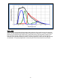
1
FASTCAMERA34 USER AND REFERENCE MANUAL FVM-50034 1 COPYRIGHT NOTICE Copyright 2009 by FastVision LLC. All rights reserved. This document, in whole or in part, may not be copied, photocopied, reproduced, translated, or reduced to any other electronic medium or machine-readable form without the express written consent of FastVision LLC. FastVision makes no warranty for the use of its products, assumes no responsibility for any error, which may appear in this document, and makes no commitment to update the information contained herein. FastVision LLC. retains the right to make changes to this manual at any time without notice. Document Name: FastCamera 34 User and Reference Manual Document Number: FVM-50034 Revision History: 1.0 February 4, 2009 2.0 November 12, 2009 Trademarks: FastVision is a registered trademark of FastVision LLC. Channel Link is a trademark of National Semiconductor Virtex is a trademark of Xilinx Inc. Windows, Windows 95, Windows 98, Windows 2000, Windows NT, and Windows XP are trademarks of Microsoft Video Savant, DVR Express, CL160 are registered trademarks of IO Industries. All trademarks are the property of their respective holders. FastVision LLC. 131 Daniel Webster Highway, #529 Nashua, NH 03060 USA Telephone: 603-891-4317 Fax: 603-891-1881 Web Site: http://www.Fast-Vision.com/ Email: [email protected], or [email protected] 2 TABLE OF CONTENTS TABLE OF CONTENTS ............................................................................................................................... 3 FAST CAMERA 34 USER MANUAL AND REFERENCE ............................................................................ 6 GETTING STARTED QUICKLY ................................................................................................................... 6 INTERFACE .................................................................................................................................................. 7 HARDWARE ................................................................................................................................................. 7 SENSOR ..................................................................................................................................................... 10 KSC-1000.................................................................................................................................................... 11 AD9945 12-BIT 40 MHZ CCD SIGNAL PROCESSOR .............................................................................. 12 XILINX FPGA .............................................................................................................................................. 13 PNX1502/PNX1702 PROCESSOR............................................................................................................. 15 SINGLE CHANNEL ANALOG I/O .............................................................................................................. 16 CAMERA LINK INTERFACE ...................................................................................................................... 16 THE INPUT POWER CONNECTOR .......................................................................................................... 17 ENVIRONMENT .......................................................................................................................................... 18 CAMERA DIMENSIONS ............................................................................................................................. 18 REFERENCE GUIDE .................................................................................................................................. 18 REGISTRY .............................................................................................................................................. 19 Write registry value ‘regw’ ..................................................................................................................................20 Read registry value ‘regr’ ....................................................................................................................................20 Dump the registry ‘regd’ .....................................................................................................................................20 Reload the registry from flash ‘regl’ ....................................................................................................................20 Save the registry to flash ‘regs’ ............................................................................................................................20 Erase all of the registry values ‘rege’ ...................................................................................................................20 Update the registry settings in RAM ‘regu’ .........................................................................................................20 Read settings from the registry in RAM ‘regp’ ....................................................................................................21 Delete an entry from the registry in RAM ‘regx’ .................................................................................................21 FPGA MODULE ...................................................................................................................................... 21 Video Transport Control, ‘vtc’ ............................................................................................................................21 Set FGPO Frequency ‘voclk’ ...............................................................................................................................21 Camera Link Power Control ‘vopwr’...................................................................................................................21 Do Read Write Register Test ‘fregt’ ....................................................................................................................21 Write FPGA Register ‘fregw’ ..............................................................................................................................21 FPGA Read Register ‘fregr’ ................................................................................................................................22 FPGA Display Image Statistics ‘fregs’ ................................................................................................................22 Display the FPGA registers .................................................................................................................................22 Display Bit Field by Name ‘bitd’ .........................................................................................................................22 Dump the Contents of Front End Memory...........................................................................................................22 Test Front End Memory.......................................................................................................................................22 Read Front End Memory into a Buffer ‘fer’ ........................................................................................................22 Write Front End Memory from a Buffer ‘few’ ....................................................................................................23 Dump Debug Registers ‘dbgd’ ............................................................................................................................23 FPGA Reset Command ‘reset’ .............................................................................................................................23 Toggle Diagnostic LED on the CPU Board ‘led’ ................................................................................................23 Read or Write a MMIO Register in the Processor ‘mmio’ ..................................................................................24 Show Progress ‘p’ ................................................................................................................................................24 Generate Test Pattern Images ‘tpat’ .....................................................................................................................24 3 FPGA Related Registry Entries ...........................................................................................................................24 UART MODULE ...................................................................................................................................... 24 Send and Receive Reply on camera link ‘cl’ .......................................................................................................24 Turn on Loop Back ‘sloop’ ..................................................................................................................................25 Registry Value ‘uart:Baud’ ..................................................................................................................................25 Registry Value ‘uart:crlf’ .....................................................................................................................................25 FGPI MODULE ........................................................................................................................................ 25 Print out the FPGI register settings ‘fgpid’ ..........................................................................................................25 Print out the FPGI interrupt counters ‘fgpiin’ ......................................................................................................25 Re-initialize the FGPI ‘fgpiri’ ..............................................................................................................................25 FGPO MODULE ...................................................................................................................................... 25 Print out the FPGO register settings ‘fgpod’ ........................................................................................................25 Print out the FPGO interrupt counters ‘fgpoin’ ...................................................................................................25 Re-initialize the FGPO ‘fgpori’ ...........................................................................................................................25 AD9945 MODULE ................................................................................................................................... 25 Read Field ‘adrf’ ..................................................................................................................................................25 Write Field ‘adwf’ ...............................................................................................................................................26 Set OB (Optical Black) Clamp value ‘adcl’ ........................................................................................................26 Set VGA gain ‘adg’ .............................................................................................................................................26 Display AD9945 registers ‘add’ ..........................................................................................................................26 Reinitialize the AD9945 registers ‘adi’................................................................................................................26 Registry variable ‘afe:0-VGAGain’ .....................................................................................................................26 Registry variable ‘afe:1-VGAGain’ .....................................................................................................................26 MEMORY MODULE ................................................................................................................................ 26 Memory Encode ‘men’ ........................................................................................................................................26 Memory Decide ‘mde’ .........................................................................................................................................27 Memory Allocate, ‘mm’.......................................................................................................................................27 Memory Free ‘mf’................................................................................................................................................27 Memory display allocations ‘mdm’ .....................................................................................................................27 Transfer to memory ‘mtc’ ....................................................................................................................................27 Transfer from memory ‘mfc’ ...............................................................................................................................27 Transfer from memory to flash ‘mtf’ ...................................................................................................................27 UTILITY MODULE................................................................................................................................... 28 Display Memory ‘dm’ ..........................................................................................................................................28 Display the Build date and time ‘built’ ................................................................................................................28 Display the command list ‘help’ ..........................................................................................................................28 Display the log buffer ‘log’ ..................................................................................................................................28 Performance timing utilities .................................................................................................................................28 Direct control of gpio pins ‘gpio’ ........................................................................................................................28 RS485 MODULE ..................................................................................................................................... 28 Rs485 Status command ‘rs485s’ ..........................................................................................................................28 Rs485 Send command ‘rs485x’ ...........................................................................................................................29 Registry variable ‘rs485:BAUD’ .........................................................................................................................29 Registry variable ‘rs485:echo’ .............................................................................................................................29 TRIGGER MODULE ................................................................................................................................ 29 Set trigger source command ‘tsrc’ .......................................................................................................................29 Manual trigger command ‘trig’ ............................................................................................................................29 MANUAL RS485 TRIGGER ‘TRX’.......................................................................................................... 29 Initalize Trigger command ‘tinit’ .........................................................................................................................29 Set the pixel clock frequency ‘xclk’.....................................................................................................................29 Set the exposure ‘exp’..........................................................................................................................................29 Set the frame period ‘fp’ ......................................................................................................................................29 Single pulse trigger command ‘tpulse’.................................................................................................................30 Trigger status command ‘tstat’.............................................................................................................................30 Set Trigger to free running command ‘tfree’ .......................................................................................................30 4 Set Trigger to external trigger command ‘ttrig’ ...................................................................................................30 Registry variable PixelClk ...................................................................................................................................30 Registry variable Exposure ..................................................................................................................................30 Registry variable FramePer..................................................................................................................................30 Registry variable ‘trig:src’ ...................................................................................................................................30 Registry variable ‘trig:pol’ ...................................................................................................................................30 Registry variable ‘trig:free’ ..................................................................................................................................30 Registry variable ‘trig:pass’ .................................................................................................................................30 KSC-1000 MODULE ............................................................................................................................... 30 KSC STATUS COMMAND ‘KSCS’ ......................................................................................................... 30 KSC initialization command ‘ksci’ ......................................................................................................................31 KSC WRITE REGISTER COMMAND ‘KSCW’ ....................................................................................... 31 KSC read register command ‘kscr’ ......................................................................................................................31 KSC reset command ‘kscc’ ..................................................................................................................................31 KSC reinitialize command ‘ksct’ .........................................................................................................................31 KSC reload settings from flash ‘kscl’ ..................................................................................................................31 KSC SAVE SETTINGS TO FLASH ‘KSCV’ ........................................................................................... 31 KSC PRINT DEFAULT SETTINGS ‘KSCP’............................................................................................ 31 KSC ADJUST SETTING ‘KSCBM’ ......................................................................................................... 31 KSC set number of sensor taps to use ‘kscnt’ ......................................................................................................31 KSC read back and check settings ‘ksc?’ ............................................................................................................31 KSC SET EXPOSURE AND NUMBER OF LINES ‘KSCE’ .................................................................... 32 Registry variable ‘ksc:spiclkper’..........................................................................................................................32 Registry variable ‘ksc:bbwrite’ ............................................................................................................................32 Registry variable ‘ksc:bbread’ .............................................................................................................................32 Registry variable ‘ksc:ntaps’ ................................................................................................................................32 Registry variable ‘ksc:FrameTable’ .....................................................................................................................32 Additional Registry Variables ‘k:*’ .....................................................................................................................32 FLAT FIELD MODULE............................................................................................................................ 33 Flat Field make dark image command ‘ffdark’ ....................................................................................................33 Flat Field make gain image command ‘ffgain’.....................................................................................................33 Flat Field find bad pixels command ‘ffbad’ .........................................................................................................33 Flat Field correction enable command ‘ffe’ .........................................................................................................33 Flat Field reload from flash ‘ffrl’ .........................................................................................................................33 Registry variable ‘ff:ngain’ ..................................................................................................................................33 Registry variable ‘ff:ndark’ ..................................................................................................................................33 Registry variable ‘ff:nfract’..................................................................................................................................33 Registry variable ‘ff:load_dark’ ...........................................................................................................................33 Registry variable ‘ff:load_gain’ ...........................................................................................................................34 Registry variable ‘ff:darkoff’ ...............................................................................................................................34 Application Specific Values ................................................................................................................................34 TROUBLESHOOTING................................................................................................................................ 35 FASTVISION TECHNICAL SUPPORT ....................................................................................................... 35 CONTACTING TECHNICAL SUPPORT ................................................................................................ 35 5 FAST CAMERA 34 USER MANUAL AND REFERENCE GETTING STARTED QUICKLY The most direct setup of the FC34 is with the single tap basic Camera Link interface and computer as diagrammed below. Other setups include RS485 communication via the Hirose power connector or serial interface which is discussed below. Computer Keyboard and Display Laptop or Desktop Computer FC34 Camera Camera Link Cable Camera Link Frame Grabber Camera Control Software Camera Link DLL Frame Grabber Software In order to access the commands in the camera you need to connect the camera to a camera link frame grabber as shown above, and run a terminal emulation program provided by your frame grabber vendor. The terminal emulation program allows you to type commands on your keyboard which are then sent to the camera on the camera link serial interface. Replies from the camera are returned on the camera link interface and displayed on your screen. Please refer to the Camera Link Standard for a detailed discussion of this process. The essentials are that a camera control program or terminal emulation program must access the camera via the frame grabber, which may require the use of the frame grabber vendor provided camera link DLL. The actual solution required is determined by your frame grabber vendor. Initially when the camera is being used for the first time a very small set of commands is needed. They are: fp <microseconds> exp < microseconds> ttrig 6 tfree ksce <exposure> <lines> „fp‟ sets the frame period (1/frame rate). It is entered in microseconds. For example a NTSC compatible frame rate you would enter „fp 33367‟ for about 29.97 Hz. „exp‟ set the exposure in microseconds. Exposure can overlap frame readout. The exposure must be less than the frame period or unexpected timing will develop. For the standard settings the frame readout time is 4.8msec. „ttrig‟ will setup the trigger input on CC1 to be positive edge sensitive. The camera will wait for a trigger to capture a frame. „tfree‟ will setup the free running trigger controlled by the „fp‟ command. „ksce‟ command allows you to reduce the number of lines in the image allowing higher frame rates. For example ksce 100 50, would set the exposure to 100 microseconds, and the number of lines in the image to 50. At this height you can run up to 1000 fps, so enter fp 1000. If you save settings to the registry while ksce operation is active, be sure to set ksc:FrameTable to zero. To return to normal operation set ksce:exp, and ksce:lines to zero and set ksc:FrameTable to four, and then save the registry (regs), and power cycle the camera. INTERFACE The camera has two electrical connectors, a base Camera Link SDR26 connector, and a Hirose 12 pin circular connector for power. The front side of the camera has the lens mount, which is a C-Mount compatible thread (32 tpi 1” diameter). The front surface of the camera is 17.526mm in front of the surface of the sensor. The back focus distance is fixed. The camera is mounted using a standard camera foot, with two 5mm screw holes and one ¼-20 screw hole. The camera can be ordered without the foot and the mounting holes for the foot can be used for mounting. HARDWARE The Fast Camera 34 (FC34) is a CCD camera based on the Kodak KAI-0340 sensor, and processing system based on the NXP PNX1702/1502 processor. The AI-340 is a 640x480 two tap sensor which can operate at up to 215 full frames per second. The processor is a 500 MHz VLIW processor (PNX1702) or a 300 MHz processor (PNX1502). A simplified block diagram of the camera system is shown below. 7 Image Data (255MB/sec) Channel Link Drivers Receivers cc1 cc2 cc3 cc4 stf stc SDR26 Base Camera Link 28b 85 MHz 256 Mbyte DDR Memory 512 mbit NOR FLASH PNX-1702/1502 16b @ 100MHz 128 Mbyte DDR2 Memory FPGA XC3S700A 12b @ 40 MHz 12b @ 40MHz AD9945 AD9945 Sensor KAI-0340 Simplified Block Diagram FC34 8 KSC-1000 Drivers Detailed Block Diagram FC34 9 SENSOR The sensor used in the FC34 is the Kodak KAI-0340 CCD sensor. The KAI-0340 is an Interline Transfer, Progressive Scan, high sensitivity, CCD sensor. The specifications of the sensor are shown in the table below. Parameter Number of Active Pixels Number of Outputs Pixel Size Active Pixels Optical Size Active Pixels Size Aspect Ratio Output Sensitivity Photometric Sensitivity Mono Color Charge Capacity Readout Noise Dynamic Range Dark Current Maximum Pixel Clock Speed Maximum Frame Rate Package Type Package Size Package Pins Package Pin Spacing Value 640 (H) x 480 (V) =307200 1 or 2 7.4μm (H) x 7.4μm (V) 5.92mm (diagonal) 1/3” optical format 4.74mm (H) x 3.55mm (V) 4:3 30 μV/e 3.61 V/lux-sec 1.17(B), 1.54(G), 0.65(R) V/lux-sec 40 MHz – 20,000 electrons 20 MHz – 40,000 electrons 40 MHz – 16 electrons 20 MHz – 14 electrons 40 MHz – 62 dB 20 MHz – 69 dB Photodiode < 200 eps VCCD < 1000 eps 40MHz 210 fps (dual output) 110 fps (single output) CerDIP 0.500” [12.70mm] width 0.625” [15.87mm] length 22 0.050” In addition to the above specifications the sensor can transfer the center approximately one third of the lines or columns to the readout electronics without having to dump lines or columns. This allows the sensor to operate at very high speed on smaller ROIs which are centered in the active area of the sensor. The table below shows the obtainable frame rates for different ROI settings and output taps. Description 640 x 480 228 x 480 640 x 164 228 x 164 228 x 55 KAI-0340-Single and KAI-0340-Dual Single Output (fps) 112 306 325 877 2000 KAI-0340-Dual Only Dual Output (fps) 214 581 618 1637 3400 The figure below shows the Quantum Efficiency of the sensor with a standard glass cover. The sensor can be purchased with a quartz window for improved efficiency below 375 nm. 10 KSC-1000 The KSC-1000 is an integrated timing generator which produces all the waveforms used to readout the sensor. This chip allows the timing of the readout waveforms to be adjusted in 1 ns steps. It controls the positioning of the horizontal and vertical clocks, clearing the sensor to start exposures, transfer of the image to interline storage, shifting of the interline storage, and horizontal readout. The two taps are connected to the right and left half of the sensor. The left tap reads out in raster order the right tap reads out backwards. The right taps digital data is reversed by the FPGA before transfer to the processor. 11 KSC-1000 Block Diagram. AD9945 12-BIT 40 MHZ CCD SIGNAL PROCESSOR The AD9945 is a complete analog signal processor for CCD applications. It features a 40 MHz singlechannel architecture designed to sample and condition the outputs of progressive scan area CCD arrays. The AD9945‟s signal chain consists of a correlated double sampler (CDS), a digitally controlled variable gain amplifier (VGA), a black level clamp, and a 12-bit A/D converter. The internal registers are programmed through a 3-wire serial digital interface (SPI). Programmable features include gain 12 adjustment, black level adjustment, input clock polarity, and power-down modes. The gain range of the VGA is x2 to x100 in 1024 steps. XILINX FPGA A Xilinx XC3S700A-4FTG256C FPGA interfaces the digital outputs of the AD9945 converters to the PNX1702 FGPI inputs. The FPGA provides the capability to process the digital video before delivery to the processor. Connected to the FPGA is 128 megabyte DDR2 memory. The function of this memory is application specific. Typically it contains the data to perform the flat field correction of the sensor, and frame buffers for algorithms which require multiple frames. An option for a larger FPGA is available. The standard FPGA does the following: Accept one or two tap data from the sensor at 12 bits Reads the correction tables from DDR2 memory. Applies the 16 bit offset values to each pixel Applies the 16 bit gain values to each pixel Optionally reformats the data for direct delivery to Camera Link. Provides a UART for the Camera Link Reverses the right tap sensor data to match the left tap. Provides the SPI interfaces to the KSC-1000 and the AD9945s Performs defective pixel correction Reports the sum of all the pixel values Reports the intensity of the brightest pixel Reports the location of the brightest and darkest pixel. 13 14 PNX1702 PROCESSOR A block diagram of the PNX1702 is shown in the diagram below. The PNX1702 processor accepts the video data from the FPGA on a 16 bit parallel interface operating at 100 MHz called the FGPI. The processor can manipulate the images before they are sent to a host computer via a Channel Link high speed parallel interface, part of the Camera Link interface on the camera, or it can process the images and signal results via RS484 or LVDS interfaces. The processor sends image data via a 28 bit parallel interface, called the FGPO, which connects directly to the 28 bits of the channel link chip. This gives the processor direct control of the image format provided to the Camera 15 Link interface. A block diagram of the processor is provided above. As an option a PNX1502 processor can be provided as they are pin compatible, to reduce the power consumption. Connected to the processor is 256MB of SDRAM which is used by the processor to run programs. In addition a 512 Mbit NOR flash is connected to provide which is used to boot the camera and holds configuration information for the operation of the camera. SINGLE CHANNEL ANALOG I/O A single analog to digital converter is provided for sampling analog voltages, along with an analog output. The standard configuration is 0 to 10 volts input /output. A LTC2630 provides the analog output. It is a 12 bit 200 KHz converter. The analog input is provided via a MCP3001 analog to digital converter. This is a 10 bit up to 200KHz device. MCP3001 LTC2630 CAMERA LINK INTERFACE The FC34 provides a base Camera Link interface for transporting images out of the camera system, or for preview / setup of the camera in embedded applications. The Camera Link interface provides 28 bits of parallel data at up to 85 MHz. In addition the Camera Link interface contains a bi-directional LVDS serial interface, which can be operated at up to 115,200 baud. Also the four discrete signals CC1 to CC4 are provided. 16 x1 x2 x3 Port C Port B Port A STF stc STC cc1 stf Enable CCIO1 cc2 clk Enable CCIO2 cc3 ck Enable CCIO3 cc4 SDR26 Camera Link Connector Channel Link Transmitter x0 FVAL LVAL DVAL Spare Enable CCIO4 FC34 Camera Link Compatible Interface The CC1 to CC4 discrete signals can be switched to outputs or can operate as RS485 outputs in embedded applications. THE INPUT POWER CONNECTOR The input power connector is a Hirose HR10A Male pins. Pin Assignments are:: Pin 1 2 3 4 5 6 7 8 9 10 11 12 Function +5 volt Ground Return +5 Volt power input -15 Volt power input +15 Volt power input Digital Ground User Definable 1 User Definable 2 Digital Ground User Definable 3 +5 Volt Ground Return +5 Volt power input User Definable 4 17 User Definable Options Description --------------------------------------------------------------------DAC Output / Analog Ground Standard configuration 0 to 10 Volts ADC Input / Analog Ground Standard configuration 0 to 10 Volts RS489+/RS485RS485 communication channel (up to 2) Trigger Input TTL up to 2 inputs Trigger Output TTL one output Trigger Input LVDS up to 2 inputs Trigger Input RS422 up to 2 inputs Recommend power supply specifications +5 Volts at 2 amps (+/- 5%) low noise +15 Volts at 0.2 amps (+/- 5%) low noise -15 Volts at 0.2 amps (+/- 5%) low noise ENVIRONMENT The camera takes power from a three output voltage external power supply. The input voltages are +/-15 volts, and +5 volts. The total power dissipated by the camera is from 5 to 8 Watts. The small size of the camera dictates a need for a conduction cooling pathway to transport heat out of the camera or forced air cooling (i.e. a fan). If the foot is installed on the camera and the camera is attached to a metal post having the area of the foot, sufficient cooling should be obtained. If air cooling is desired blow at least 25 lfm of air flow. The primary cooling surface is the bottom of the foot or fins if present. The camera can operate reliably at up to a 55 degree case temperature. Be sure to provide either air bottom of the camera where the foot is cooling or conduction cooling to keep the case below 55 degrees. CAMERA DIMENSIONS REFERENCE GUIDE The software in the FC34 is built with the PNX NDK 5.8 software development system for the PNX1502 and PNX1702 processors. It is beyond the scope of this document to explain the operation and use of the PNX NDK5.8. 18 In this section a description of the various commands implemented in the camera is provided. Depending on how the camera has been customized more commands may exist. The typical setup for a user of the camera is a laptop or desktop computer containing a camera link frame grabber, which provides terminal access to its associated serial interface. The camera supports a command / response style interface for changing settings and modifying the operation of the camera. Commands are entered much like a command Window in Windows. Each hardware element has a software module which provides control functions, storage, and a command set to access its functionality from the command line interface. Each „module‟ supports commands like Initialize, load parameters, save parameters, and get command list. Many of the commands were created for testing and debugging the various camera elements, these commands are retained for developers who customize the camera to their own application. The diagram below gives a representation of the various software and hardware modules with arrows indicating of data flows. Flat Fld Module FGPI Module Application FGPO Module RS485 Module FGPI AFML FGPO GPIO PNX 1702 Device Libraries FPGA Registry Module Memory Module NOR Flsh . Camera Link ADC Module KSC Module Trigger Module UART Module AD9945 KSC-1000 Triger UART Memory NOR Flsh FPGA Module Video FPGA Library Utilities Module PNX 1702 Device Libraries AD9945 KSC-1000 Camera Link Serial Camera For the typical user the frame rate, exposure, and trigger mode are of main interest. To adjust the frame rate use the „fp‟ command, to adjust the exposure use the „exp‟ command, and finally the trigger is controlled by the „tsrc‟, „ttrig‟, and „tfree‟ commands. See Getting Started below for the details of these commands. REGISTRY A portion of the NOR Flash (1MB) is reserved for the storage of settings and other data which must survive a power cycle. The registry supports 5 data types, byte, short, long, float, and string. Values are stored in the registry by their name. The name is up to a 50 character string, not containing white space. The commands for manipulating the registry are listed in the following sections. On power up the registry is copied into RAM to improve access times. On command the registry in RAM can be updated from the various software modules internal values, or the modules can reload their settings from the registry in RAM. The registry in RAM can be reloaded from flash or saved to flash. Finally the registry in RAM values can be viewed, or changed via the registry command line interface. 19 Configuration values reside in three locations, in the software module which takes care of programming the hardware, in the registry in RAM, and in the registry in NOR flash. Registry Copy in RAM Software Module Configuration Varriables regp Configuration Varriables regu Registry in Flash regl Configuration Varriables regs regw regr regx Write registry value ‘regw’ This command updates registry values or creates new registry values. The syntax is shown below. The <type> entry can be „b‟ for byte, „s‟ for short, „l‟ for long, „f‟ for float, and „x‟ for string. If the registry value doesn‟t exist and the type is missing, an error is indicated that the type is missing. If the entry doesn‟t exist and the type is given a new entry is created. Finally if the entry exists its value is updated. Note: you cannot change the type of an entry if it exists in the registry, you have to delete it (regx) and create it again. regw <name> <value> [b|s|l|f|x] The registry variable <name> is any sequence of characters not including white space. White space is any of the characters 0x09,0x0a,0x0b,0x0c,0x0d, and 0x20, or the using the names of these characters <tab>,<line feed>,<vertical tab>,<new page>,<carriage return> and <space>. Names are case sensitive. The <value> is read with „C‟ format functions so the formats acceptable to scanf, will be read correctly. If the value exceeds the size of the type it is truncated. If the value contains a decimal point (period), then it will be read with a %f format. If the value starts with „0x‟ it is read as a hex value with a %x format. Otherwise the value is read with a %d format. If the type is string, the value is saved as a string, the same rule as that of the name applies the value string; it cannot have any embedded white space. Read registry value ‘regr’ The read registry command looks up a value in the registry and prints it on the console. If it doesn‟t exist an error message is generated indicating that. The syntax of the read registry command is: regr <name> Dump the registry ‘regd’ This commands prints out all the entries in the registry Reload the registry from flash ‘regl’ This command reads the registry from flash over writing the registry in RAM. Any unsaved values in RAM are lost. Save the registry to flash ‘regs’ This command saves the registry in RAM to the flash. Erase all of the registry values ‘rege’ This command deletes all the values in the RAM registry. If this is saved all the entries are lost permanently. This is not as bad as it seems, the defaults can be loaded by doing a regu command followed by a regs command. This is to be avoided if possible because each camera is adjusted differently at the factory for an optimal image. The default settings are good, but not as good as they can be. Don‟t use this command if possible. Update the registry settings in RAM ‘regu’ 20 This command causes all of the hardware modules to save their variables into the registry in RAM. Commands that modify the state of the hardware typically do not update the registry, so if you get the camera setup the way you want it, do a regu and then a regs to save it. If for some reason you decide that your current settings are no good do a regp to reload the values in the modules from the RAM registry, or power the camera off and then on. Read settings from the registry in RAM ‘regp’ This command causes all the modules to read their settings from the registry in RAM and update their respective hardware components. (regp = registry parse). Use this command if the registry in RAM contains more desirable values than those currently programmed in the hardware. Delete an entry from the registry in RAM ‘regx’ This command will delete an entry from the registry. There is no undo, but the entry is printed before it is deleted. The syntax is: regx <name> FPGA MODULE The FPGA module provides commands that access functionality in the FPGA that is not associated with some other major chip, like the KSC-1000 and the AD9945 which have their own modules even though they are accessed through the FPGA. The following sections describe the commands provided by the FPGA Module. Video Transport Control, ‘vtc’ Video transport refers to the part of the program which receives images from the FPGA, processes them and then sends them to Camera Link. This command is typically not used by a user of the camera, it primarily is used during software debug. The syntax of the command is: vtc [start | stop] The start command, starts up the video transport tasks. The stop command tells the video transport tasks to exit. Set FGPO Frequency ‘voclk’ This command is used to set the clock rate of the camera link output. Any value between 20 MHz and 85 MHz is supported (in steps of 1MHz). The syntax of the command is: voclk <number> Where <number> is the desired clock frequency in MHz. You may want to set this for compatibility with the frame grabber you are using, or to slow delivery of images to the host computer. Delivery of images to camera link is not tightly coupled in the standard camera. Images can be provided by the FPGA to the processor, while the process may not provide all of them to the Camera Link output. Camera Link Power Control ‘vopwr’ This command allows the user to turn off the camera link output to conserve power or to provide more memory bandwidth to the PNX processor in the camera. The syntax of the command is: vopwr [on | off] Do Read Write Register Test ‘fregt’ This command reads and writes values to the selected register. This is used to test the camera in production and during software debug. The format of the command is: fregt <register> Where <register> is a valid FPGA register number. This command should not be used by an end user of the camera. Write FPGA Register ‘fregw’ This command is used to write a value to one of the FPGA registers. The syntax of the command is: fregw <register> <value> 21 FPGA Read Register ‘fregr’ This command is used to read the current contents of an FPGA register. The syntax of the command is: fregr <register> FPGA Display Image Statistics ‘fregs’ This command prints out the last image statistic collected by the FPGA. It includes the following values: Count of the number of pixel that were used in these results Value of the brightest pixel Location of the brightest pixel (x,y) Value of the darkest pixel Location of the darkest pixel (x,y) Sum of all the pixel values counted. The count of the number of pixels used to compute these values can be less than the full complement of pixels in the sensor because defective pixels are excluded from this processing. A defective pixel is one whose gain in the correction tables is set to zero. The syntax of the command is: fregs Display the FPGA registers This function will display the values written to the FPGA registers and reads and displays the contents of the read registers. The values written to the FPGA registers cannot be read back but they are saved in memory for display by this command. The syntax of this command is: fregd Display Bit Field by Name ‘bitd’ The command displays a bit field from the FPGA registers, so that it does not have to be extracted by hand. The bit fields defined are list in the FPGA Description Document. Dump the Contents of Front End Memory This function displays the contents of the front end memory connected to the FPGA. In the current FPGA the front end memory contains the calibration values for the flat field correction of the image. The syntax of the command is: fed <address> <length> Where the <address> is the starting 16 byte page to start the display from. The <length> is how many 16 byte pages to display. The minimum read and write size for the front end memory is 16 bytes. The maximum length that can be displayed is 4 MB. Test Front End Memory This command writes a random patter to a buffer, moves it the front end memory, reads it back and checks that the values read match the values written. This command was used in the debug of the camera hardware and is used to locate detect defects in the production of the cameras. It is not normally needed by the end user. Note: the front end memory contains the flat field correction tables which will be trashed by the memory test. They can be reloaded from flash if they were saved, or they can be regenerated by repeating the flat field calibration procedure. Read Front End Memory into a Buffer ‘fer’ This command is used to copy the contents of front end memory to a buffer in the processors memory. The syntax of the command is: fer <address> <length> Where <address> is the 16 byte block to start from, and <length> is the number of 16 byte blocks to copy. The buffer used is the „fgpi_buffer‟. This command was used in the debug of the hardware of the camera and should not be used by the end user. 22 Write Front End Memory from a Buffer ‘few’ The command takes the contents of the „fgpi_buffer‟ and writes it to front end memory. The syntax of this command is: Few <address> <length> Where <address> is the 16 byte block to start writing to, and <length> is the number of 16 byte blocks to write. This command was used in the debug of the camera hardware and should not be used by the end user. Dump Debug Registers ‘dbgd’ This command was created during the debug of the camera hardware but still has some utility to the end user. The command displays the following information: Status of LVAL from the camera to the FPGA Status of FVAL from the camera to the FPGA Status of the Pixel clock Status of the Operate bit (Enables FPGA functions) Status of VD from the FPGA to the KSC-1000 Status of the CAMON bit. (Not used anymore) „Line Length‟ or the number of pixel clocks LVAL is active „Line inactive‟ or the number of pixel clocks LVAL is inactive The Number of lines FVAL is active „_Data‟ or the most recent values read from the left and right DACs. „VDI_start_count‟ or the number of message starts sent to the processor. „VDI_stop_count‟ or the number of message stops sent to the processor „VDI_dv_count‟ or the number of active pixels in an image The number of frames detected by the FPGA. If the camera is generating images then LVAL, FVAL, pixel clock, and the frame count should be changing. If not the likely cause is miss programming of the KSC-1000. The FPGA will update the Line length, the line inactive and the number of lines per frame if it is detecting images from the camera. The VDI start and stop counts indicates the number of images sent to the processor. If the FPGA is providing images to the processor, these values should be changing. Note: they will not be identical in value because they aren‟t read at the same time from the FPGA. The VDI DV count is the number of pixels sent to the processor in the last message. All of these values should be changing if the camera and FPGA are operating correctly. FPGA Reset Command ‘reset’ This command pulses the output on the processor that indicates to the FPGA it should reset. The pulse is 50 msec long. The syntax of this command is: reset It depends on the FPGA design being used what this does. Toggle Diagnostic LED on the CPU Board ‘led’ This command toggles LEDs on / off inside the camera. The LEDs are only visible when the cover of the camera is removed. The syntax of the command: led <pin> <value> When <pin> is zero to three, and value is zero for low (LED On), one for high (LED off), or two to toggle the state. LED zero and one are on the CPU card. LED two and three are on the driver card, and are not installed. LED two and three can be one single two color LED as well. As the LEDs are inside the camera case this command is not very useful to the end user. 23 Read or Write a MMIO Register in the Processor ‘mmio’ The command is used to manually change the values in a register in the processors (PNX1702). This command is not useful to an end user because all of the MMIO settings are handled by software, and are not saved in the NOR flash. The syntax of the command is: mmio <offset> [<value>] When <offset> is the byte offset to the register from the MMIO base address. If <value> is given a write to the provided offset is performed followed by a read back. Show Progress ‘p’ This command cause the software to print out a status message every ten seconds which contains the frame rate, the time it took to send a frame to camera link, the number of images generated by the FPGA and the number of images processed by the processor, and the first few pixels from an image. The syntax of the command is „p‟ there is no parameters. Enter „p‟ again to stop the messages. Generate Test Pattern Images ‘tpat’ This command causes the processor to generate test pattern images and to send them to camera link. The type of test pattern is selected by the number following the command. The test patterns are: 0 – No test pattern 1 - black 2 - white 3 - walking vertical bar 4 - walking horizontal bar 5 - gradient left to right 6 - gradient top to bottom 7 - diagonal gradient top/left to bottom/right 8 - complement of input image FPGA Related Registry Entries The FPGA module supports several settings in the registry. These settings are read out on power up and cause the camera to change state. Name f:Rstats f:CamLnkOn f:REV f:VDM Verbose Camera# f:BAUDV TheSensorIsColor f:ksce:exp f:ksce:lines Type Long Long Byte Byte Long Long Byte Long Long Long Default 1 1 23 0 0 0 2 0 0 0 Function Read the statistics register after each image Turn on the camera link FPGA Revision FPGA video output mode Turns on various kinds of diagnostic output Informational not used Baud rate select value, for the camera link, 2=9600 Informational not used (yet) Special timing mode value Special timing mode value UART MODULE The UART Module controls the camera link UART in the FPGA. Send and Receive Reply on camera link ‘cl’ This command sends a string to the camera link serial port. This command is only useful when the system is being debug on a JTAG emulator. 24 Turn on Loop Back ‘sloop’ This command turns on loop back so what is sent is what is received on the camera link serial lines. The connection to the camera link connector is ignored in this mode, the loop back occurs in the FPGA. Registry Value ‘uart:Baud’ This value sets the baud rate of the camera link serial on power on. Enter one of the following baud rates: 9600, 14400 19200, 28800, 38400, 57600, 115200, 230400, 460800, and 921600. Registry Value ‘uart:crlf’ Normally the cameras serial output sends only new lines (0x0A) at the end of each line. Some terminals need a new line and a carriage return, set this to one to get 0x0D,0x0A at the end of each line. FGPI MODULE Print out the FPGI register settings ‘fgpid’ This prints out the FPGI register settings which is not to useful to an end user, but is useful to software developers. Print out the FPGI interrupt counters ‘fgpiin’ This command prints out the FGPI interrupt counters. This can be used to determine if any images are being received by the processor, from the FPGA. Re-initialize the FGPI ‘fgpiri’ This command will clear an overrun condition or a HBE error on the FGPI. FGPO MODULE Print out the FPGO register settings ‘fgpod’ This prints out the FPGO register settings which is not to useful to an end user, but is useful to software developers. Print out the FPGO interrupt counters ‘fgpoin’ This command prints out the FGPO interrupt counters. This can be used to determine if any images are being sent by the processor to the camera link transmitter. Re-initialize the FGPO ‘fgpori’ This command will clear an overrun condition or a HBE error on the FGPO. AD9945 MODULE The AD9945 module controls the settings of the AD9945. While access to the registers is provided for testing, the power on defaults for all but the VGA gain should be unchanged for normal operation. Read Field ‘adrf’ The command reads a named bit field from one of the registers. The bit field names is shown below. The prefix „0-„ applies to the left side AD9945, while the prefix „1-„ applies to the right side AD9945. 0-SWRest 1-SWRest 0-Power 1-Power 0-OBCLDis 1-OBCLDis 0-PBLKLev 1-PBLKLev 0-SHP/SHDPol 1-SHP/SHDPol 0-DataclkPol 1-DataclkPol 0-CLBPol 1-CLBPol 0-PBLKPol 1-PBLKPol 25 0-OutDis 0-DataLatch 0-DataCode 1-OutDis 1-DataLatch 1-DataCode Please see the data sheet for the AD9945 for the function of this bit fields. The default for all of these is zero. The Syntax of this command is: adrf <bit-field-name> Write Field ‘adwf’ This command can be used to write the bit fields. The syntax for this command is adwf <bit-filed-name> <value> Set OB (Optical Black) Clamp value ‘adcl’ This command will set the optical black clamp value, which will disable the function of the optical black clamp circuit. This command is only used in testing. The syntax of this command is: adcl <value> Set VGA gain ‘adg’ This command is used to set the VGA gain. It can take the value zero to 1023. Zero generates a 2 to 1 gain (3dB), 1023 generates a 100 to 1 gain (40dB). Typically this should be set to 300. It can be manipulated for low light situations which will also affect the readout noise. The syntax for this command is: adg <value > [0|1|2] The value selects the gain, 1 selects the left cannel only, 2 the right channel, zero or no digit changes both channels. Display AD9945 registers ‘add’ This command prints the contents of all the two AD9945 devices. The syntax for this command is: add Reinitialize the AD9945 registers ‘adi’ This command zeros all the registers and loads the VGA gain from the registry values. The syntax of this command is: adi Registry variable ‘afe:0-VGAGain’ The registry variable saves the VGA gain in the registry for the left channel. It is restored to the hardware on power up and the „adi‟ command. It can take the value 0 to 1023. Higher values will be truncated to this range. Registry variable ‘afe:1-VGAGain’ This is the matching registry variable for the right channel. MEMORY MODULE These commands are used to control memory in some special applications and during software development. They are not useful to the end user. Memory Encode ‘men’ This command takes binary data from memory and converts it to base-64 data to be sent via the camera link serial port, to a connected host. The syntax of this command is: men <src> <length> The resulting encoded buffer is output to the display. „<src>‟ is the address in memory to get the binary data from, and length is the number of bytes to be encoded. 26 Memory Decide ‘mde’ This command takes base-64 input and converts it to binary in the called out buffer. The syntax of this command is: mde <dst> <length> The resulting decoded base-64 input is written as binary to the destination called out by <dst> for at most the provided length. The base-64 steam can end before the length is exhausted. Memory Allocate, ‘mm’ This command is used to allocate a buffer in memory for whatever reason. The buffer is isolated memory from the application and other software running in the camera and can be used for any purpose until it is released with the „mf‟ command. The syntax of this command is: mm <size> „<size>‟ is the desired size in bytes for the allocated memory block. The address of the block is returned. Memory Free ‘mf’ This command release a memory block back to the camera OS. Use this command when you don‟t need the memory block anymore. The syntax of the command is: mf <ptr> Where <ptr> is the address returned by the „mm‟ command. Note the pointer is checked against the allocations recorded, if it does not match one of the previously allocated buffers the command prints an error and does nothing. Memory display allocations ‘mdm’ This command will display any un-free-ed memory allocations. The syntax is „mdm‟. Transfer to memory ‘mtc’ This command takes data from the serial port and transfers it to memory at the specified address. The syntax of the command is: mtc <addr> Where <addr> should be the address returned by a mm command or any know to be safe areas. Transfer from memory ‘mfc’ This command transfers data from memory to the serial port. The syntax of the command is: mfc <addr> <length> The address is the location of the data to be transferred, the length is the length in bytes to transfer. Transfer from memory to flash ‘mtf’ This command is used to transfer memory into flash so its contents will be preserved across power downs. If the command is given without any parameters, in the debug version of the software it will program the boot area in flash with the release version of the software built into the debug version. The syntax of this command is: mtf [<addr> <length>] The user must know that the target area in flash is free to be overwritten by the provided data. The user should take care with this command as it can trash the content of flash and require the camera be reprogrammed with a development system, or at the factory. 27 UTILITY MODULE The utility module contains commands that didn‟t have enough functionality to warrant an module of their own, or for historical reasons ended up as a utility command. Display Memory ‘dm’ This command displays the contents of memory. The syntax of the command is: dm <addr> <length> <step> The <addr> can be a number or an alpha identifier. See the source code for this functionality. The length of the display is in the units called out by the step if present else it is in bytes. The step size selects bytes (1), shorts (2), or longs (4). If the step is left off then bytes is assumed. Display the Build date and time ‘built’ This command displays when the software was last built. The syntax of the command is „built‟. Display the command list ‘help’ This command will list the commands that are supported by all the modules in the system or for a given module if its name is given. The syntax of the command is: help [<mod-name>] Display the log buffer ‘log’ This command displays the content of the log buffer. This buffer contains a listing of the last several hundred commands or diagnostics which can be placed there by software but not displayed on the console. The syntax of the command is „log‟. The content of the log is erased after it is printed. Performance timing utilities These commands are used by developers to time performance of software. See the source code module time.c for the use of these commands. stik Start time etik End time rtik Print time ttik Trigger time mtik <mode> <pttc> Tick Mode time Direct control of gpio pins ‘gpio’ This command is used by developers to control the GPIO pins on the processor during debugging of code. Consult the schematic for the connectivity of the GPIO pins and the GPIO pin number. gpio <#> [<value>] This command should not be used by end users. RS485 MODULE The RS485 Module controls the RS485 drivers used to implement the CC1 to CC4 signals in the camera link interface. For normal operation of the camera link interface the RD485 drivers are not enabled, they are used as receivers for data from the frame grabber connected to the FC34. Rs485 Status command ‘rs485s’ This command prints out the status of the rs485 interface. It will print Rs485 Call Back count ### Indicating that the application callback has received „###‟ characters from RS485. 28 Rs485 Send command ‘rs485x’ This command transmit a string to the selected RS485 channel. The syntax of the command is: rs485x <chan> <string> Where <chan> is the channel digit 0 to 3 for CC1 to CC4, and <string> is what is to be sent. Registry variable ‘rs485:BAUD’ This variable memorializes the desired baud rate for the rs485 channels. One rate applies to all four channels. Registry variable ‘rs485:echo’ The variable causes the replies sent to the camera link serial port (serial to Frame Grabber) to be echoed to rs485 channel two (CC2). TRIGGER MODULE The Trigger module controls the frame rate, exposure, the source and type of trigger input, the pixel clock rate and the manual trigger. Set trigger source command ‘tsrc’ The syntax of this command is tsrc [g|c|b|n] [+|-] |t] [b|n] The first parameter controls the source of the trigger, „g‟ means use GPIO2 on the processor, „c‟ uses CC1, „b‟ use both GPIO2 and CC1, and „n‟ there is no external trigger. The second parameter selects the polarity of the trigger „+‟ is positive edge, „-„ is negative edge. The final parameter is used for testing, „b‟ means bypass the trigger logic and use GPIO2 for the trigger, and „n‟ for normal operation. GPIO2 is used to generate software triggers (i.e. using the „trig‟ command or using a function call in the camera application). The „c‟ setting uses the camera link input signal CC1. Manual trigger command ‘trig’ This command will trigger the camera from the command line. It has no parameters. MANUAL RS485 TRIGGER ‘TRX’ This command will stimulate the application with a fake trigger from rs485. This command only works with applications that have implemented it. Initalize Trigger command ‘tinit’ This command re-initializes the trigger settings from the registry variables. Set the pixel clock frequency ‘xclk’ This command selects the pixel clock frequency. It should not be used as the current settings are designed for 40 MHz clock rate. The parameter is one of 10, 20 or 40 for the desired frequency in megahertz. Set the exposure ‘exp’ This command sets the exposure. The parameter to the command is the number of microseconds desired. Set the frame period ‘fp’ This command sets the frame period in microseconds. This is only significant in free run. The frame period command sets an free running trigger source from the FPGA. The exposure can affect the actually delivered frame rate. The frame readout time subtracted from the exposure time must be less than the frame period. The frame readout time is about 4.8 msec. 29 Single pulse trigger command ‘tpulse’ This command sends a single pulse to the ksc-1000 as a trigger. Depending on the frame tables being used this may generate a frame or it may not. Is some application two pulses are required. Trigger status command ‘tstat’ This Is an application specific command and typically prints the number of triggers and the number of result messages sent. Set Trigger to free running command ‘tfree’ This command sets the trigger to use the free running trigger source in the FPGA, whose period is set with the „fp‟ command. Set Trigger to external trigger command ‘ttrig’ This command sets the trigger to use the external input either software command (GPIO2) or external pulse (CC1). Registry variable PixelClk This variable memorializes the desired pixel clock rate on power up. Its value can be 10, 20 or 40. It should be left at 40 for 40MHz. Registry variable Exposure This variable memorializes the exposure desired on power up. Registry variable FramePer This variable memorializes the desire frame period on power up. Registry variable ‘trig:src’ This variable memorializes the trigger source on power up. It can be 1 for CC1, 2 for GPIO2 or 3 for both. Registry variable ‘trig:pol’ This variable memorializes the trigger polarity on power up. It can be 1 for positive edge 0 for negative endge. Registry variable ‘trig:free’ This variable memorializes the desired trigger mode on power up. It can be 0 for triggered and 1 for free run. Registry variable ‘trig:pass’ This variable memorializes the mode for the GPIO2 pass thru trigger. It should be zero. KSC-1000 MODULE This module controls the sensor timing and readout. In order to understand these settings you will need to understand the detailed block diagram at the beginning of this document and the data sheet for the KSC1000 from Kodak. It is too difficult to explain how the KSC-1000 works and how you might change these variable. Do not change any of these settings without consulting the factory. KSC STATUS COMMAND ‘KSCS’ This command reads out the KSC status register it prints (for example): FGPI Interrupts = 401423 KSC dll_locked = 1 KSC frame table address = T7:E4 KSC line table address = T1:E3 KSC VD registered = 0 KSC VD wait = 0 KSC line counter = 0 30 KSC initialization command ‘ksci’ This command sends the settings stored in the module to the KSC chip. It prints: Starting ksc_init 013456789 013456789 Finished ksc_init Any other output is likely to be an error indication. KSC WRITE REGISTER COMMAND ‘KSCW’ This command changes settings in the registers of the KSC. Don‟t use this command. Syntax: kscw reg val val val KSC read register command ‘kscr’ This command reads out and prints the contents of a KSC register. It is safe to use this command. Syntax: kscr <reg> Where <reg> is zero to 9. KSC reset command ‘kscc’ This command pulses / sets / resets the KSC reset input. If you uses this command the KSC will stop operating, and a „ksci‟ command will be required. Don‟t use this command. Syntax: kscc [ p | 0 | 1 ] KSC reinitialize command ‘ksct’ This command does a slightly different reset re-initialization of the KSC. Do not use this command. Ksct KSC reload settings from flash ‘kscl’ This command reloads the KSC settings from flash. It is not used anymore, use regl and regp. Syntax: kscl KSC SAVE SETTINGS TO FLASH ‘KSCV’ This command saves the KSC settings to flash. It is not used anymore, use regu and regs. SyntaxL kscv KSC PRINT DEFAULT SETTINGS ‘KSCP’ This command prints out the default settings for the KSC for the current operating mode. Syntax: kscpd KSC ADJUST SETTING ‘KSCBM’ This command is used to change settings of the KSC. Do not use this command. Syntax: kscbm <up|down|set|get> <name> [value] KSC set number of sensor taps to use ‘kscnt’ This command changes the number of sensor taps to use. It should be left on 2. Syntax: kscnt [1|2] KSC read back and check settings ‘ksc?’ This command checks the settings of the KSC. It prints: 013456789 On success. Anything else is an error. Syntax: ksc? 31 KSC SET EXPOSURE AND NUMBER OF LINES ‘KSCE’ This command sets the exposure and the number of lines desired in the output image. It changes the settings of the KSC to do a partial frame readout, which shortens the frame readout time, as well as programs the exposure delay into the KSC. This command disables the „exp‟ command until the camera is rebooted with a power cycle. Syntax: ksce <exposure> <nlines> Exposure it in microseconds. Registry variable ‘ksc:spiclkper’ This variable controls the timing of the SPI interface to the KSC. It should be left at 150. Its units are nanoseconds. Registry variable ‘ksc:bbwrite’ This variable controls how the KSC chip is accessed. It must be set to one for proper operation. Registry variable ‘ksc:bbread’ This variable controls how the KSC chip is accessed. It must be set to one for proper operation. Registry variable ‘ksc:ntaps’ This variable memorializes the power on setting for the number of taps from the sensor to use. It should be left at 2. Registry variable ‘ksc:FrameTable’ This variable selects which frame table the KSC should start using. It should be 4 unless the ksce mode (reduced number of lines in the image) is being used; in this case it should be zero. Additional Registry Variables ‘k:*’ These variables are used by the KSC module to save settings for the KSC controller in flash. The variable is patterned k:<ksc-register>:<camera-mode>:<name>, for example k:1:0:ppl is the pixels per line value for full frame single tap mode readout which is programmed into register 1 of the KSC chip. Please see the KSC-1000 data sheet for an explanation of these values. These values do not need to be changed unless non-standard frame formats are needed. Name Value Name Value Name Value Name Value k:1:0:ppl 720 k:1:1:ppl 384 k:1:2:ppl 246 k:1:3:pp 121 k:1:0:lvs 0 k:1:1:lvs 45 k:1:2:lvs 0 k:1:3:lvs 0 k:1:0:lve 708 k:1:1:lve 371 k:1:2:lve 244 k:1:3:lve 120 k:1:0:cobs 180 k:1:1:cobs 180 k:1:2:cobs 180 k:1:3:cobs 180 k:1:0:cobe 1680 k:1:1:cobe 140 k:1:2:cobe 1220 k:1:3:cobe 140 k:1:0:cobs 228 k:1:1:cobs 2740 k:1:2:cobs 2464 k:1:3:cobs 26 k:1:0:cobe 234 k:1:1:cobe 2380 k:1:2:cobe 2242 k:1:3:cobe 24 k:1:0:cdms 140 k:1:1:cdms 140 k:1:2:cdms 140 k:1:3:cdms 140 k:1:0:cdme 1680 k:1:1:cdme 140 k:1:2:cdme 1220 k:1:3:cdme 140 k:1:0:cdms 214 k:1:1:cdms 224 k:1:2:cdms 2242 k:1:3:cdms 22 k:1:0:cdme 234 k:1:1:cdme 234 k:1:2:cdme 2226 k:1:3:cdme 23 k:1:0:pblks 708 k:1:1:pblks 384 k:1:2:pblks 228 k:1:3:pblks 120 k:1:0:pblke 0 k:1:1:pblke 0 k:1:2:pblke 0 k:1:3:pblke 0 Name Value Name Value Name Value Name Value k:4:0:int 1500 k:4:1:int 1122 k:4:2:int 1244 k:4:3:int 1366 k:4:0:int 2122 k:4:1:int 2244 k:4:2:int 2366 k:4:3:int 20 k:4:0:int 3244 k:4:1:int 3366 k:4:2:int 30 k:4:3:int 30 k:4:0:int 4366 k:4:1:int 40 k:4:2:int 40 k:4:3:int 40 k:6:0:shp1o 34 k:6:1:shp1o 34 k:6:0:shp2o 34 k:6:1:shp2o 34 k:6:0:shd1o 63 k:6:1:shd1o 63 32 k:6:0:shd2o k:6:0:dck1o k:6:0:dck2o 63 54 54 k:6:1:shd2o k:6:1:dck1o k:6:1:dck2o 63 54 54 FLAT FIELD MODULE This module contains commands to collect dark and bright field calibration images and to compute and save the correction tables, and the bad pixel table. Flat Field make dark image command ‘ffdark’ This command will cause the camera to average „ff:ndark‟ dark images. The user must make sure that no light enters the camera during this operation. After the dark image is captured it is written to flash. Flat Field make gain image command ‘ffgain’ This command will cause the camera to average „ff:ngain‟ bright images. The user must make sure that no pixel is saturated and the average brightness is set to about 75% of full scale. After the bright image is obtained, gain coefficients are used to set all the pixel values to 3,000 counts out of 4095. The gain values are stored with „ff:nfract‟ fractional bits. After the gain image is computed it is saved in the flash. Flat Field find bad pixels command ‘ffbad’ This command reviews the dark and bright field images and labels pixels bad if their offset or gain values differ by more 15% for more than ½ of the nearest neighbors. The gain value is set to zero, which is used by the FPGA to replace the bad pixels with the previous good pixel value. If the parameter „clear‟ is provided all of the preexisting bad pixels are forgotten and a new set is computed. Flat Field correction enable command ‘ffe’ This command is used to enable or disable, dark field and bright field correction of camera images. Syntax: ffe [e|d] [d|g|b] Where the first parameter indicates enable („e‟) or disable („d‟) the correction type selected by the second parameter, where „d‟ means dark field, „g‟ means gain field and „b‟ means both corrections. Flat Field reload from flash ‘ffrl’ This command will read the saved flat field correction values from the flash and program the FPGA with the values. Registry variable ‘ff:ngain’ This registry variable determines how many images are averaged to get the bright field image used for calibration. This variable should be set high enough show the shot noise averages away. Shot noise is proportional to the square root of the brightness of the pixel, and it is reduced by the square root of the number of images averaged. This means if the brightest pixel is near saturation at 4095, then you need to average 4095 images to reduce the shot noise below one bit. Registry variable ‘ff:ndark’ This registry variable determines how many images are averaged to get the dark field image. At 40 MHz pixel clock the readout noise is ~16 electrons, so at least 256 images should be average to get the readout noise below one electron. Registry variable ‘ff:nfract’ This variable determines how many fractional digits are contained in the 16 bit gain value. It is application dependent what value should be used here. If the light field is particularly non-uniform then fewer fraction digits may be needed. For the default setting of 13, the range of gain value obtainable is 0 to x8. Registry variable ‘ff:load_dark’ When this registry variable is set to one, the dark field table will be loaded from flash on power up and dark field correction will be enabled. 33 Registry variable ‘ff:load_gain’ When this registry variable is set to one, the gain field table will be loaded from the flash on power up and the gain correction will be enabled. Registry variable ‘ff:darkoff’ This value is added to each pixel to offset the „black‟ level above zero to avoid clipping the noise. Application Specific Values As the camera can be customized to an end user‟s application the variables mentioned in this section may or may not exist in the users version of the camera. The values app:axx,app:axy,app:bx, app:ayx, app:ayy, and app:by are the coefcients of an affine transform which is applied to the pixel coordinates to convert to the users coordinate system. 34 TROUBLESHOOTING There are several things you can try before you call FastVision Technical Support for help. _____ Make sure the camera and power supply are plugged in. Make sure the power source is on. _____ Make sure you have followed the installation instructions for all the software. _____ If you are developing software for use inside the camera be sure you installed the software correctly according to the software installation instructions. _____ Insert the FastVision CD-ROM and check the various Release Notes to see if there is any information relevant to the problem you are experiencing. FASTVISION TECHNICAL SUPPORT FastVision offers technical support to any licensed user during the normal business hours of 9 a.m. to 5 p.m. EST. We offer assistance on all aspects of processor board and PMC installation and operation. CONTACTING TECHNICAL SUPPORT To speak with a Technical Support Representative on the telephone, call the number below and ask for Technical Support: Telephone: 603-891-4317 If you would rather FAX a written description of the problem, make sure you address the FAX to Technical Support and send it to: Fax: 603-891-1881 You can email a description of the problem to [email protected] Before you contact technical support have the following information ready: _____ Part numbers, serial numbers and hardware revision numbers for the camera. This information is printed on a label affixed to the camera and also on your packing list that was shipped with your camera. _____ The version on the software you are using whether provided by FastVision or a third party. _____ The type and version of the host operating system, i.e., Windows XP. _____ Note the types and numbers of all your software revisions, daughter card libraries, the application library and the compiler. Please indicate which development tools and version you are using if you‟re a developing software for use with the camera. _____ Returning Products for Repair or Replacements 35 Our first concern is that you be pleased with your FastVision products. If, after trying everything you can do yourself, and after contacting FastVision Technical Support, you feel your hardware or software is not functioning properly, you can return the product to FastVision for service or replacement. Service or replacement may be covered by your warranty, depending upon your warranty. The first step is to call FastVision and request a “Return Materials Authorization” (RMA) number. This is the number assigned both to your returning product and to all records of your communications with Technical Support. When a FastVision technician receives your returned hardware or software he will match its RMA number to the on-file information you have given us, so he can solve the problem you‟ve cited. When calling for an RMA number, please have the following information ready: _____ Serial numbers and descriptions of product(s) being shipped back _____ A listing including revision numbers for all software, libraries, applications, etc. _____ A clear and detailed description of the problem, a method of duplicating the problem and when it occurs _____ If software that you have developed is required to duplicate the failure please provide it. _____ A description of the camera set up and any environmental condition that can cause the problem All of this information will be logged into the RMA report so it‟s there for the technician when your product arrives at FastVision. Put boards inside their anti-static protective bags. Then pack the product(s) securely in the original shipping materials, if possible, and ship to: FastVision LLC. 71 Spit Brook Road, Suite 200 Nashua, NH 03060 USA Clearly mark the outside of your package: Attention RMA #90XXX Remember to include your return address and the name and number of the person who should be contacted if we have questions. Reporting Bugs We at FastVision are continually improving our products to ensure the success of your projects. In addition to ongoing improvements, every FastVision product is put through extensive and varied testing. Even so, occasionally situations can come up in the fields that were not encountered during our testing at FastVision. If you encounter a software or hardware problem or anomaly, please contact us immediately for assistance. If a fix is not available right away, often we can devise a work-around that allows you to move forward with your project while we continue to work on the problem you‟ve encountered. It is important that we are able to reproduce your error in an isolated test case. You can help if you create a stand-alone code module that is isolated from your application and yet clearly demonstrates the anomaly or flaw. Describe the error that occurs with the particular code module and email the file to us at: [email protected] 36 We will compile and run the module to track down the anomaly you‟ve found.If you do not have Internet access, or if it is inconvenient for you to get to access, copy the code to a disk, describe the error, and mail the disk to Technical Support at the FastVision address below. If the code is small enough, you can also: FAX the code module to us at 603-891-1881 If you are faxing the code, write everything large and legibly and remember to include your description of the error. When you are describing a software problem, include revision numbers of all associated software. For documentation errors, photocopy the passages in question, mark on the page the number and title of the manual, and either FAX or mail the photocopy to FastVision. Remember to include the name and telephone number of the person we should contact if we have questions. FastVision LLC. 131 Daniel Webster Highway, #529 Nashua, NH 03060 USA Telephone: 603-891-4317 FAX: 603-891-1881 Web site: http://www.FastVision.com/ Electronic Mail: [email protected] [email protected] 37