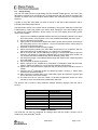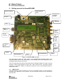
1
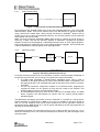
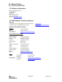
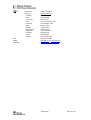
C
CC1100/CC1150DK
&
CC2500/CC2550DK
Development Kit User Manual
Rev. 1.2
Supported chips:
SWRU040A
Table of contents
1.
2.
3.
4.
5.
Introduction ..................................................................................................................... 3
About this manual ........................................................................................................... 3
Definitions ....................................................................................................................... 3
What can I do with this development kit? ....................................................................... 4
Getting started ................................................................................................................ 4
5.1
Powering the Evaluation Board................................................................................... 4
5.2
Range testing .............................................................................................................. 6
5.3
Running examples ...................................................................................................... 7
5.4
RF testing .................................................................................................................... 7
5.4.1
Output power testing............................................................................................ 8
5.4.2
Sensitivity testing ................................................................................................. 8
5.5
Using the SmartRF®04DK for prototyping................................................................... 9
6.
Getting around the SmartRF04EB................................................................................ 10
6.1
USB Interface............................................................................................................ 10
6.2
RS-232 interface ....................................................................................................... 11
6.3
User interface............................................................................................................ 11
6.4
Audio interface .......................................................................................................... 11
6.5
SMA test connectors ................................................................................................. 11
6.6
I/O connectors........................................................................................................... 12
6.7
EM connectors .......................................................................................................... 13
6.8
Signal flow................................................................................................................. 14
6.9
SmartRF®04EB Schematics...................................................................................... 15
7.
CC1100EM ................................................................................................................... 18
8.
CC1150EM ................................................................................................................... 21
9.
CC2500EM ................................................................................................................... 23
10.
CC2550EM ................................................................................................................... 25
11.
Firmware ....................................................................................................................... 26
12.
SmartRF®04EB programming model............................................................................ 27
12.1
The bootloader ...................................................................................................... 27
12.2
Making bootloader compliant applications ............................................................ 27
12.3
The USB MCU....................................................................................................... 29
13.
SmartRF®04DK troubleshooting tips ............................................................................ 30
14.
Document history.......................................................................................................... 30
14.1
Disclaimer.............................................................................................................. 31
14.2
Trademarks ........................................................................................................... 31
15.
Address Information...................................................................................................... 32
16.
TI Worldwide Technical Support................................................................................... 32
SWRU040A
1. Introduction
Thank you for purchasing a CC1100/CC1150DK or CC2500/CC2550DK Development Kit!
Please note that SmartRF®04DK is used as a collective term in this document, representing
the development kits on the SmartRF®04 platform (CC1100/CC1150DK and
CC2500/CC2550DK).
The SmartRF®04DK development platform supports evaluation, development and prototyping
using the SmartRF®04 products from Chipcon.
Make sure to subscribe to the Chipcon Newsletter to receive information about updates to
documentation, new product releases and more. Sign up on the Chipcon web site. Signing up
ensures that you are informed when this and other documents are updated with new
important information.
2. About this manual
This manual contains both tutorial and reference information, and covers both the hardware
and software components of the development kit. SmartRF® Studio has its own user manual.
Examples and libraries are also covered in a separate document.
This manual is organized with the tutorial information located at the start, and the reference
information towards the end.
We recommend reading the “What can I do with this development kit?” and “Getting started”
sections first, and then refer to the reference information when needed.
Further background information can be found in the SmartRF® Studio User Manual and the
device datasheets.
3. Definitions
SmartRF®04DK
USB MCU
Factory firmware
PER
SoC
EM, Evaluation
Mode
SmartRF®04EB, EB,
Evaluation Board
A collective term used for all development kits for the SmartRF®04
platform, i.e. CC2500/CC2550DK and CC1100/CC1150DK.
The Silicon Labs C8051F320 MCU used to provide a USB interface
on the SmartRF®04EB.
The firmware that is programmed into the USB MCU from the factory.
This firmware supports SmartRF® Studio operation as well as a standalone PER tester.
Packet Error Rate. Measures the percentage of packets that contain
errors or are lost.
System on a Chip. A collective term used to refer to Chipcon ICs with
on-chip MCUs (future products).
A small module containing a radio IC and the needed external
components. Also serves as a reference design for how to make a
PCB layout using the radio IC. For example CC2500EM contains a
CC2500 and associated external components.
A motherboard for the various EM boards. Contains various user
interface circuitry, a USB MCU and a USB interface that can be
connected to a PC.
SWRU040A
Page 3 of 33
4. What can I do with this development kit?
The development kit is designed to help the user to achieve his/hers objectives as quickly as
possible using Chipcon’s products.
•
•
•
Evaluate the SmartRF®04 products. Right out of the box, the user can do range
testing (PER testing) and transfer data from one PC to another using the
SmartRF®04DK. This enables the user to quickly find out how well the SmartRF®04
products fit the intended application. A number of demonstration applications serve to
highlight the innovative features of the SmartRF®04 ICs.
Perform RF measurements. Using SmartRF® Studio, the user can configure the radio
ICs with parameters that suit the intended application and easily measure sensitivity,
output power and other RF parameters.
Develop a prototype. The SmartRF® 04DK includes a Silicon Labs 8051-core MCU
with 16 kB of program memory and 1 kB of data memory. By programming this MCU
and utilizing the various peripherals included on the Evaluation Board, the user can
easily make a prototype of the intended application. All signals are brought out on
0.1” pin-row connectors so easy connection of other required circuitry is possible.
These connectors are also compatible with Agilent logic analyser probes for easy
debugging. It is also possible to disconnect the Silicon Labs MCU from the EM board,
and connect a MCU selected by the user to the I/O connectors.
5. Getting started
This section describes how to perform the most common tasks associated with the
development kit.
Please see the Quick Start instructions included with the Development Kit for step-by-step
information on how to set up your kit.
Please note that operation with modules for earlier ICs (CC1000, CC1010, CC1020, CC1070,
CC2400, CC2420) is not supported. Use the appropriate development kit instead (CC1000
RF modem or CC1000DK for CC1000. CC1020/CC1070DK for CC1020, CC1021 and
CC1070. CC2400DK for CC2400. And CC2420DK for CC2420).
Make sure to install SmartRF® Studio before connecting the Evaluation Board to a PC.
SmartRF® Studio can be downloaded from Chipcon’s web pages.
5.1
Powering the Evaluation Board
Figure 1. Power terminal block
•
•
The 4-10V input is used for powering the Evaluation Board using the on-board
voltage regulator.
0V is the ground connection.
SWRU040A
Page 4 of 33
•
•
The 3.3V terminal is used for powering the Evaluation Board, bypassing the on-board
voltage regulator. A voltage between 2.7-3.6V can be used when USB is not active.
When using USB the voltage should be limited to 3.0-3.6V.
When shipped from the factory, a jumper is placed between I_OUT and I_IN. To
measure the current draw of just the EM, the jumper can be removed and the current
can be measured using an amperemeter or multimeter between the I_OUT and I_IN
terminals. Make sure to replace the jumper when you are finished measuring the
current.
The SmartRF® 04EB can be powered in several different ways:
• DC power from a laboratory power supply or battery eliminator power supply. The DC
jack connector accepts standard DC jack power connectors with a 2.5mm center pin.
The center pin is used for the positive voltage, and the sleeve for ground.
If a laboratory power supply is used, ground should be connected to the 0V terminal
on the power terminal block (see Figure 1).
A 4-10V supply can be connected to the “4-10V” terminal, or a 3.3V supply can be
connected to the “3.3V” terminal. If a 3.3V supply is used, the supply selection switch
should be set to the “3.3V” position, otherwise the “4-10V” position should be used. If
the “4-10V” position is selected, a voltage regulator supplies the circuitry on the
board. Otherwise the 3.3V supply is applied directly to the EB, bypassing the
regulator.
• USB power. If the EB is connected to a USB socket on a PC, it will draw power from
the USB bus. The onboard voltage regulator supplies 3.3V to the board.
• Battery power. The evaluation board includes a 9V-type battery connector on the
bottom side of the PCB. A 9V battery or a battery pack that uses a 9V-type connector
can be connected to this battery connector. The onboard voltage regulator supplies
3.3V to the board.
If several power sources are connected simultaneously, the Evaluation Board will be powered
from the supply that supplies the highest voltage.
Figure 2. Power switch setting (3.3V position)
The Power Switch S3 must be set according to what power source is used. If 3.3V is applied
using the power terminal block, the switch should be set to the left position as shown in Figure
2 above. In all other cases, the switch should be set to the right position for power to be
applied to the Evaluation Board. This switch can be used to turn off the EB by switching it to
the opposite position of that used to turn it on.
Please note that while the SmartRF04® devices have a very wide supply range, the
components on the Evaluation Board limit the total voltage supply range to 2.7V – 3.6V (3.0V
– 3.6V while the USB is active). The Evaluation Board is designed for a temperature range of
–40°C to +85°C (excluding the LCD display). The Evaluation Module is designed for a
temperature range of -40°C to +85°C.
SWRU040A
Page 5 of 33
5.2 Range testing
The user can easily perform range testing with the SmartRF®04DK right out of the box. This
description assumes that the MCUs are pre-programmed with the required firmware (the
firmware is loaded onto the Evaluation Board before the development kit is shipped from
Chipcon).
A guide to using the PER tester can also be found on the Quick Start Instruction that is
included within the development kit.
The PER tester uses a menu system that is controlled by the joystick. Selecting a menu item
is performed by moving the joystick up or down, while changing a menu item setting is done
by moving the joystick sideways. Arrows shown on the LCD display show what joystick
motions are possible.
1. Plug two CC1100EM/CC2500EM modules into the two Evaluation Boards. The range
test uses two-way communication, so the CC1150EM/CC2550EM cannot be used.
2. Connect antennas to both EMs.
3. Apply power to the Evaluation Boards and set the power selector switch according to
the used power source. See chapter 5.1 for more information about various ways of
powering the Evaluation Board.
4. Press the S1 button to start the PER program.
5. Select the frequency band to be used. Make sure that this is in accordance with the
EM module placed in the EB board (e.g. 2.4 GHz for the CC2500EM).
6. Set an ID for the EB. The two EBs that are going to communicate need to have the
same ID. The reason for supporting different IDs is so that multiple pairs of EBs can
run multiple PER tests simultaneously without disturbing each other.
7. Set the packet length. The selected packet length will influence the measured packet
error rate (PER).
8. Set the number of packets to transmit.
9. Select a preset to use. Presets set a combination of modulation, data rate and other
settings. Please see below for a list of what the different presets mean.
10. Select mode. The board that is configured with the above options should be set as a
master.
11. Configure the 2nd Evaluation Board by performing steps 3 through 7. Select slave
mode on this Evaluation Board.
12. Start the test by scrolling down to the “Start PER” option and press the joystick right
first on the slave, then on the master.
13. The PER test will run until the number of packets programmed earlier has been
reached, or until 100 consecutive packets have been lost.
The joystick can be used to select between different statistics displays while the test is
running.
Preset no.
0
1
2
3
0
1
2
3
CC1100
10 kbps GFSK
1.2 kbps GFSK
38.4 kbps GFSK
500 kbps MSK
CC2500
10 kbps FSK
250 kbps MSK
250 kbps MSK with FEC
500 kbps MSK
Table 1. Preset list
The PER test can also be configured for settings other than the built-in presets. This is
achieved by using SmartRF® Studio.
SWRU040A
Page 6 of 33
Select the PER tab in SmartRF® Studio “Normal view”, and program the master unit with
wanted settings or use the SmartRF® Studio “preferred settings”. Note that it is necessary to
run the PER tester once from SmartRF® Studio to ensure that the new settings are written to
the EB firmware. When this is done preset 3 contain the new settings (default preset 3 is
overwritten by SmartRF® Studio), so when the EB is disconnected from the USB and
SmartRF® Studio it is possible to run the PER test in stand-alone mode with the new settings
by selecting preset 3. As with the preloaded PER tester, the slave unit should be started
before the master unit.
Be aware that the PER tester firmware will overwrite some registers even if these are tried
changed from register view. The PER tester requires that normal mode and variable packet
length is used. It also requires that CRC check is enabled and that the status bytes are
appended to the RX FIFO.
When a PER test using non-default settings is finished and the EB is connected to SmartRF®
Studio, the software will detect that the EB firmware is different from the factory shipped
firmware. SmartRF® Studio will prompt the user with a message that the EB contains old
firmware. Select “yes” and the factory firmware will be loaded back onto the EB.
Please also note that the built-in PER test for CC1100 uses 0dBm output power as default. To
test maximum range it is necessary to increase the output power using SmartRF® Studio.
When the 10dBm output power is used the two EB boards should be placed at least 1m apart
when starting the PER test to avoid saturation effects and errors in the PER test start-up.
5.3 Running examples
The SW examples provided by Chipcon can easily be run on this platform. SmartRF® Studio
can be used to load different .hex files into the USB MCU. Note that the examples have to be
linked with the bootloader libraries to work (all examples provided from Chipcon have been
linked with these libraries).
Connect the Evaluation Board to a PC using the USB interface. Make sure that an EM board
is plugged into the Evaluation Board before applying power. Start SmartRF® Studio and select
the SmartRF®04 tab. Select the “CCxxxx – new device” (do not choose the “Calculation
Windows”) and click on the “Load USB Firmware” button. A file selection dialog box is then
presented, and the file to download can be selected. Please see the Examples and Libraries
document for more information.
Note that when the USB interface is connected to a PC, it is necessary to press the S1 button
to exit the bootloader and start the example.
5.4 RF testing
RF testing is best performed by using SmartRF® Studio together with the Evaluation Board.
Connect the EB to a PC using the USB interface. Start the SmartRF® Studio and select the
SmartRF®04 tab. Select the correct Evaluation Board (several Evaluation Boards can be
connected to a PC at once), it should be listed as “CC2500 – new device” (or CC2550,
CC1100, CC1150), and click the Start button. The main SmartRF® Studio window is then
opened. In this window the user can select settings, perform tests and adjust registers. RF
measurement equipment may be connected to the SMA connector on the EM.
Please see the SmartRF® Studio documentation for more information about the operation of
SmartRF® Studio.
SWRU040A
Page 7 of 33
5.4.1
Output power testing
EB+EM
RF carrier
Spectrum analyzer
Figure 3. Output power (conducted) measurement set up
Plug an EM into the SmartRF®04EB, and connect the Evaluation Board to a PC using USB.
Start SmartRF® Studio. Connect the antenna port of the EM board to a spectrum analyser
using a 50-ohm RF coaxial cable. Use the simple TX function in SmartRF® Studio to set up
the RF chip to emit a carrier at the desired frequency. An accurate measure of the conducted
output power can now be made.
Make sure that a resolution bandwidth (RBW) large enough to capture all the RF energy is
used (e.g. 3 MHz), and that the spectrum analyzer is calibrated. If possible the spectrum
analyzer should be checked against a calibrated instrument such as a RF signal generator.
Using good-quality RF cabling the loss in the cabling should be negligible, but the actual loss
is also included when checking against a RF signal generator.
5.4.2
Sensitivity testing
BER tester
PN sequence
RF signal
generator
RF signal
EB+EM
Received data+clock
Figure 4. Sensitivity measurement set up
For proper sensitivity testing a bit-error rate tester is needed. The exact setup will depend on
the specific brand of tester you are using, but in general the setup is as follows:
• The BER tester generates a pseudo-random baseband signal. This is used to
modulate an RF signal generator (in some cases the BER tester is integrated in the
RF signal generator). The modulated RF signal is then fed into the antenna connector
of the EM.
• The RF chip should be configured to operate in non-buffered mode, outputting the
received bit stream on the general I/O pins that are routed to the DTEST1 and
DTEST2 SMA connectors on the Evaluation Board.
• The demodulated signal and clock are then fed back to the BER tester. The BER
tester compares the demodulated bit stream with the original pseudo-random
baseband signal.
The BER tester will display the number of errors measured in a scientific (i.e. 5E-6) format.
Usually sensitivity is measured for a BER of 1E-3, but it is possible to use other criteria as
well. To find the sensitivity limit the RF power delivered by the RF generator should be
decreased until the BER equals 1E-3. The RF power delivered by the RF signal generator at
this point is the sensitivity figure.
An alternative measure of the sensitivity limit is to use a certain packet error rate (e.g. 1%) to
define the sensitivity limit. In this case the sensitivity limit will also vary with the length of the
received packet.
SWRU040A
Page 8 of 33
5.5 Using the SmartRF®04DK for prototyping
There are two main options for prototyping: The on-board Silicon Labs C8051F320 USB MCU
can be used, or an external MCU found suitable for the application can be interfaced through
the available pin-row connectors on the SmartRF®04EB.
When using the on-board USB MCU, the user can utilise the examples and libraries provided
by Chipcon to speed up development. Please see the Examples and Libraries User Manual
for more details. Table 10 on page 29 shows what pins on the MCU are used for different
functions.
If extra circuitry that is not present on the SmartRF®04EB is needed, the P10 and P11 pin-row
connectors can be used to connect the Evaluation Board to another PCB or prototyping board
with the required circuitry. See Table 2 on page 12 and Table 3 on page 12 for the pin-out of
these connectors.
If using another MCU is preferred, there are two options. Either a custom PCB can be used
and then connect the EM to this PCB, or a custom PCB (or a MCU development board) can
be connected to the SmartRF®04EB.
When choosing the first option, the EMs can easily plug into a custom board if Samtec TFM110-02-S-D-K-A connectors are included on the custom board. Make sure to place the
connectors 1200 mils apart (centre to centre). Table 4 on page 13 shows the pin-out of these
connectors.
For the second option, the 0-ohm resistors are removed to isolate the USB MCU from the EM
selectively for all signals (see Figure 6 on page 14 for details, the schematics show what
resistor controls what signal). Once this is done, the P10 and P11 connectors can be used to
interface the EM to a custom MCU PCB or development board. Once modified, the Evaluation
Board will not work with SmartRF® Studio or the examples before the 0-ohm resistors are
placed back on the SmartRF®04EB.
SWRU040A
Page 9 of 33
6. Getting around the SmartRF04EB
Power connector
Supply selection
switch
Connectors for
evaluation
modules
DC jack
SMA test
connectors
LCD
USB
connector
USB MCU
debug
connector
RS-232
connector
Pot
Headphone
output
USB MCU
reset
Mic.
input
Button
S1
Joystick
I/O connector A
I/O connector B
LEDs
Volume
control
Figure 5. SmartRF®04EB overview
The figure above shows the major parts of the SmartRF®04EB Evaluation Board. The
Evaluation Board serves as the main platform in the development kit and is designed so that it
will support future Chipcon ICs as well.
The core component is the Silicon Labs C8051F320, a USB MCU based on an 8051 core that
includes 16 kB of Flash program memory and 1 kB of data memory. This MCU provides
interfacing to SmartRF® Studio via USB and controls the rest of the Evaluation Board in
stand-alone mode.
6.1 USB Interface
The USB interface is used to interface to a PC to run SmartRF® Studio. It is also possible to
reprogram the USB MCU via this interface, and the Evaluation Board can be bus-powered
from the USB.
SWRU040A
Page 10 of 33
6.2 RS-232 interface
The RS-232 can be used by custom applications for communication with other devices. It is
not used in the factory firmware. The RS-232 interface utilises a voltage translation device so
that the RS-232 port is compatible with bipolar RS-232 levels.
Note that this RS-232 level converter contains a charge-pump power supply that is quite
noisy. It is possible to disable this by driving a pin on the USB MCU low (this pin is also used
to disable the headphone amplifier). Worst case, this noise could disturb the radio under
some conditions.
6.3 User interface
The Evaluation Board includes a joystick and a push button as user input devices, and four
LEDs and a 2x16 character LCD display as user output devices.
The factory pre-programmed firmware uses the joystick, S1 push button and LCD display to
implement a menu system used to control the packet error rate handling.
6.4 Audio interface
The SmartRF04®EB includes a microphone input and headphone output that is used by some
of the examples to provide audio I/O.
The audio output section consists of a volume control, followed by a 4th order Chebyshev
filter. This filter serves to attenuate frequencies above 6 kHz, and so converts the PWM signal
to an analog audio signal. A headphone amplifier IC (TPA4411 from Texas Instruments) is
used to drive the headphones.
Note that the headphone amplifier IC uses switch-mode power supply techniques to generate
a negative noise, and this may cause electrical noise. The headphone amplifier can be
disabled by driving a pin on the USB MCU low (the same pin is used to disable the RS-232
voltage converter).
The audio input section consists of a microphone amplifier that also includes a low-pass antialiasing filter.
A standard PC-type headset with separate microphone and headphone mini-jacks can be
connected directly to the audio interface.
6.5 SMA test connectors
The SMA test connectors on the SmartRF04®EB allow easy connection of coaxial cables to
various GDO, SPI and I/O lines on the EM.
The different lines can be routed to the SMA test connectors in several different
configurations using jumpers and 0 ohm resistors. See Figure 13 , page 18 for details.
SWRU040A
Page 11 of 33
6.6 I/O connectors
The I/O connectors bring out all the signals from the EM connectors. These connectors are
compatible with Agilent logic analyser probes for easy probing of signals. These connectors
also make it easy to connect additional external circuitry using a ribbon cable to connect to a
prototyping board, for instance.
Pin
1
2
3
4
5
6
7
8
9
10
11
12
13
14
15
16
17
18
19
20
Function
Mic input
+3.3V
+3.3V
Push button
RS-232 RD
RS-232 TD
RS-232 RTS
Joystick push, RS-232 CTS
Joystick
Potmeter
GND
Table 2. I/O connector A (P10) pin-out
Pin
1
2
3
4
5
6
7
8
9
10
11
12
13
14
15
16
17
18
19
20
Function
+3.3V
LED4
LED1
CC25XX/CC11XX GDO0
Audio output
CC25XX/CC11XX GDO2
LED2
SDA (LCD display)
LED3
SCL (LCD display)
CC25XX/CC11XX CSn
CC25XX/CC11XX SCLK
CC25XX/CC11XX SI
GND
CC25XX/CC11XX SO/GDO1
GND
Table 3. I/O connector B (P11) pin-out
SWRU040A
Page 12 of 33
6.7 EM connectors
This is where the evaluation module is connected to the SmartRF®04EB. P1 and P2 form the
main interface.
Note that while it is possible to plug in evaluation modules not belonging to the SmartRF®04
product range into the Evaluation Board, the factory firmware and SmartRF® Studio do not
support the use of older chips.
In other words, it is possible to write firmware for use with older chips and to prototype using
the SmartRF®04EB together with the older chips. However, to use SmartRF® Studio with the
older radio ICs it is necessary to use the correct development kit platform (CC2400EB for
CC2400EM and CC2420EM, or CC1020/CC1070DK for CC1020EM and CC1070EM).
EM
connector
pin
P1 pin 1
P1 pin 2
P1 pin 3
P1 pin 4
P1 pin 5
P1 pin 6
P1 pin 7
P1 pin 8
P1 pin 9
P1 pin 10
P1 pin 11
P1 pin 12
P1 pin 13
P1 pin 14
P1 pin 15
P1 pin 16
P1 pin 17
P1 pin 18
P1 pin 19
P1 pin 20
P2 pin 1
P2 pin 2
P2 pin 3
P2 pin 4
P2 pin 5
P2 pin 6
P2 pin 7
P2 pin 8
P2 pin 9
P2 pin 10
P2 pin 11
P2 pin 12
P2 pin 13
P2 pin 14
P2 pin 15
P2 pin 16
P2 pin 17
P2 pin 18
P2 pin 19
P2 pin 20
USB MCU
function
P2.4
P2.6
P2.7
P1.3
P1.7
P0.5
P2.0
P0.4
P0.6
P1.2
P0.7
P1.4
P0.3/SS
P2.1
P0.0/SCK
P1.6
P0.2/MOSI
P0.1/MISO
Transceiver
(CC2500/
CC1100)
function
GND
Transmitter
(CC2550/
CC1150)
function
GND
Comments
LED4
RTS
LED3
Push button
LED1
UART RD
LED2
UART TD
GDO0/ATEST
GDO0/ATEST
Debug interface
Mic. input
GDO2
Debug interface
PWM Sound output
CSn
CSn
SCLK
SCLK
SI
GND
SO/GDO1
SI
GND
SO/GDO1
GND
GND
GND
GND
GND
VDD
GND
VDD
GND
GND
VDD
GND
VDD
GND
GND
GND
GND
GND
GND
GND
Joystick
Pot
P2.3
P1.0
P1.5
P1.1
P2.2
Peripherals
LCD reset
Joystick push
DD_DIR
LCD SDA
CTS
LCD SCL
DD_DIR
Table 4. EM connector pin out
SWRU040A
Page 13 of 33
6.8 Signal flow
The signal lines from the EM connectors run via 0-ohm resistors to the USB MCU and the
various peripherals on the Evaluation Board. I.e. the signal lines can be disconnected from
the USB MCU by removing the 0-ohm resistors. The signal lines can then be controlled by for
instance another MCU development board by connecting to the I/O connectors. The I/O
connectors are located on the “outside” of the 0-ohm resistors, so they are still connected to
the EM connectors when the 0-ohm resistors are removed.
Please refer to Table 10 on page 29 for a list of what resistors correspond to which signals.
EM connector
0-ohm resistor
USB
MCU
Peripheral
I/O connector
Figure 6. Evaluation Board Signal flow
SWRU040A
Page 14 of 33
6.9
SmartRF®04EB Schematics
Figure 7. SmartRF®04EB schematic, page 1
Figure 8. SmartRF®04EB schematic, page 2
SWRU040A
Page 15 of 33
Figure 9. SmartRF®04EB schematic, page 3
Figure 10. SmartRF®04EB schematic, page 4
SWRU040A
Page 16 of 33
Figure 11. SmartRF®04EB schematic, page 5
Figure 12. SmartRF®04EB schematic, page 6
SWRU040A
Page 17 of 33
Figure 13. SmartRF®04EB schematic, page 7
Revision
1.4 (PCB 1.4)
1.9 (PCB 1.8)
Description/Changes
Initial public release
Component footprints improved for production.
P7 and P8 moved so that 9V battery does not conflict with pins on U301.
Added single-bit dual-supply bus transceiver for GDO0/DD.
Added 2 SMA connectors for test purposes.
Updates to the 10uF capacitor from 25V to 6.3V.
Minor modifications to +3.3V power routing.
Added P3 for MISO/MOSI interchange.
Table 5. SmartRF®04EB change list
7. CC1100EM
The CC1100EM contains the CC1100 chip and all the necessary external components. There
are different CC1100EM versions for the 315, 433, and 868/915MHz bands,
The CC1100EM contains a 26MHz crystal with +/- 10ppm initial tolerance and +/- 10ppm
temperature drift in the range 0 to + 50°C. The load capacitors used are 16pF.
A 56kΩ 1% resistor is used to set up a biasing current for the CC1100. The components
connected to the RF pins of the CC1100 perform matching to 50 ohms, balanced to
unbalanced conversion and filtering of harmonics. It is very important to copy the reference
design exactly when making your own design in order to achieve optimum RF performance. A
white box in silkscreen shows the extents of the RF layout, everything inside this box should
be copied exactly. Everything outside of the box can be changed freely.
The rest of the components on the EM are used for power-supply decoupling.
Gerber files and full documentation for the CC1100EM can be downloaded from the Chipcon
web site.
SWRU040A
Page 18 of 33
Figure 14. CC1100EM 315MHz schematic
Figure 15. CC1100EM 433MHz schematic
SWRU040A
Page 19 of 33
Figure 16. CC1100EM 868/915MHz schematic
Figure 17. CC1100EM assembly
Revision
1.0 (PCB 1.0)
Description/Changes
Initial public release
Table 6. CC1100EM change list
SWRU040A
Page 20 of 33
8. CC1150EM
The CC1150EM contains the CC1150 chip and all the necessary external components.
The CC1150EM contains a 26MHz crystal with +/- 10ppm initial tolerance and +/- 10ppm
temperature drift in the range 0 to + 50 degrees C. The load capacitors used are 16pF.
A 56kΩ 1% resistor is used to set up a biasing current for the CC1150. The components
connected to the RF pins of the CC1150 perform matching to 50 ohms, balanced to
unbalanced conversion and filtering of harmonics. It is very important to copy the reference
design exactly when making your own design in order to achieve optimum performance. A
white box in silkscreen shows the extents of the RF layout, everything inside this box should
be copied exactly. Everything outside of the box can be changed freely.
The rest of the components on the EM are used for power-supply decoupling.
Gerber files and full documentation for the CC1150EM can be downloaded from the Chipcon
web site.
Figure 18. CC1150EM 315MHz schematic
SWRU040A
Page 21 of 33
Figure 19. CC1100EM 433MHz schematic
Figure 20. CC1100EM 868/915MHz schematic
SWRU040A
Page 22 of 33
Figure 21. CC1150EM top assembly
Revision
1.1 (PCB 0.3)
1.2 (PCB 0.3)
Description/Changes
Initial public release
BOM changes on all frequency versions
Table 7. CC1150EM change list
9. CC2500EM
The CC2500EM contains the CC2500 chip and all the necessary external components.
The CC2500EM contains a 26MHz crystal with +/- 10ppm initial tolerance and +/- 10ppm
temperature drift in the range 0 to + 50°C. The load capacitors used are 16pF.
A 56kΩ 1% resistor is used to set up a biasing current for the CC2500. The components
connected to the RF pins of the CC2500 perform matching to 50 ohms, balanced to
unbalanced conversion and filtering of harmonics. It is very important to copy the reference
design exactly when making your own design in order to achieve optimum RF performance. A
white box in silkscreen shows the extents of the RF layout, everything inside this box should
be copied exactly. Everything outside of the box can be changed freely.
The rest of the components on the EM are used for power-supply decoupling.
Gerber files and full documentation for the CC2500EM can be downloaded from the Chipcon
web site.
SWRU040A
Page 23 of 33
Figure 22. CC2500EM schematic
Figure 23. CC2500EM assembly
Revision
1.0 (PCB 0.2)
2.0 (PCB 1.0)
Description/Changes
Initial public release
New PCB, Component C42 is removed from the BOM
Table 8. CC2500EM change list
SWRU040A
Page 24 of 33
10. CC2550EM
The CC2550EM contains the CC2550 chip and all the necessary external components.
The CC2550EM contains a 26MHz crystal with +/- 10ppm initial tolerance and +/- 10ppm
temperature drift in the range 0 to + 50°C. The load capacitors used are 16pF.
A 56kΩ 1% resistor is used to set up a biasing current for the CC2550. The components
connected to the RF pins of the CC2550 perform matching to 50 ohms, balanced to
unbalanced conversion and filtering of harmonics. It is very important to copy the reference
design exactly when making your own design in order to achieve optimum performance. A
white box in silkscreen shows the extents of the RF layout, everything inside this box should
be copied exactly. Everything outside of the box can be changed freely.
The rest of the components on the EM are used for power-supply decoupling.
Gerber files and full documentation for the CC2550EM can be downloaded from the Chipcon
web site.
Figure 24. CC2550EM schematic
SWRU040A
Page 25 of 33
Figure 25. CC2550EM top assembly
Revision
1.0 (PCB 0.2)
2.0 (PCB 1.0)
Description/Changes
Initial public release
New PCB
Table 9. CC2550EM change list
11. Firmware
When shipped, the SmartRF®04EB is pre-programmed with the USB bootloader and firmware
that allows the Evaluation Board to communicate with SmartRF® Studio and run a standalone packet error rate (PER) test.
This PER test is very useful when testing range, for instance to observe how many packet
errors occur and how this changes with distance and other changing conditions.
A tutorial on using the PER tester can be found in chapter 5.2 on page 6. The Quick Start
Instructions supplied within each development kit also provides a detailed walk-through of
using the PER tester application.
SWRU040A
Page 26 of 33
12. SmartRF®04EB programming model
Note that to download programs to the USB MCU without using the bootloader, it is
necessary to purchase the Silicon Labs’ EC2 serial adapter.This adapter should be connected
to P301 (marked “USB MCU debug” on the SmartRF®04EB).
Figure 26. EC2 serial adapter
Standard 8051 tools may be used, as long as they can generate HEX output files. All Chipcon
examples and libraries for the CC1100/CC1150DK and CC2500/CC2550DK are compiled
with the Keil C compiler for the 8051 platform.
Chipcon provides libraries that make it easy to control the various peripherals on the
Evaluation Board. Please refer to the Examples and Libraries document for more information
about these libraries. Please refer to Silicon Labs’ datasheet for technical information about
the USB MCU.
12.1 The bootloader
The bootloader allows the user to program new code into the USB MCU without having
access to Silicon Labs’ serial adapter or USB debug adapter. The bootloader communicates
with SmartRF® Studio or a custom programming program via USB. The Evaluation Board is
programmed with the bootloader when it is shipped from the factory.
In order to work with the bootloader, programs have to be linked with the bootloader library.
The bootloader is first and foremost a tool so that users without access to Silicon Labs’
development environment can test the various examples provided by Chipcon. When
planning to do software development, it is recommended to purchase Silicon Labs’ EC2 serial
adapter or USB debug adapter. This will also enable easy debugging of programs.
12.2 Making bootloader compliant applications
All the example code provided from Chipcon in source code form is for both stand-alone use
and for use together with the bootloader. It is possible for the user to write applications that
are compliant with the SmartRF®04EB bootloader by following the steps below:
•
Target Options
In the C51 tab: Move the reset vectors to address 0x0800
•
startup.a51
Either copy startup.a51 from another bootloader compliant application, or make the
following modifications manually before adding it to the project:
Move the reset address to 0x0800:
CSEG
AT
0x0800
SWRU040A
Page 27 of 33
?C_STARTUP:
LJMP
STARTUP1
Remove the startup code that clears the internal data memory - at least the
parts that are used by the bootloader:
IF IDATALEN <> 0
MOV R0,#IDATALEN - 1
CLR A
IDATALOOP:
MOV @R0,A
DJNZ R0,IDATALOOP
ENDIF
•
Add the file bootloader_reservations.c to the project. This file can be found in the
folder: ..\LIB\Chipcon\srf04\bootloader_reservation
•
Add the file app_descriptor.a51 to the project. This file can be found in the folder:
..\INC\CHIPCON\srf04
•
CLOCK_INIT() and IO_PORT_INIT() macros should NOT be included in the
application code, as this is taken care of by the bootloader
•
Add ebsrf04_bootloader.LIB and/or halsrf04_bootloader.LIB as needed, instead of
ebsrf04.LIB / halsrf04.LIB.
SWRU040A
Page 28 of 33
12.3 The USB MCU
The USB MCU is a C8051F320 from Silicon Labs. Please refer to the Silicon Labs web site
for more information pertaining to this MCU, such as datasheet, development tools and so on.
The following table shows what pins on the USB MCU are used for what functions.
Pin
no.
1
Pin name
(USB MCU)
P0.1
Signal name (on EB
schematic)
P1.7/SO/GDO1/MISO
0-ohm
resistor
R101
2
10
11
12
13
P0.0
P3.0/C2D
P2.7
P2.6
P2.5
P1.5/SCLK
R115
P1.3/LED3
P0.4/RTS
RS232_POWER
R113
R100
14
15
P2.4
P2.3
P2.0/LED_4
RESET_N
R120
16
P2.2
SOC_PRESENT
17
P2.1
P0.6/JOY
R106
18
19
20
21
22
23
24
25
26
27
P2.0
P1.7
P1.6
P1.5
P1.4
P1.3
P1.2
P1.1
P1.0
P0.7
P1.1/LED2
P1.0/LED1
P0.7/POT
P0.5/JOY_PUSH
P1.2/PWM_OUTPUT
P0.1/BUTTON_PUSH
P0.0/MIC_INPUT
P2.4/SCL
P2.3/SDA
P2.2/GDO2/DC
R111
R110
R107
R112
R105
R101
R104
R124
R123
R122
28
P0.6/CNVSTR
P2.1/GDO1/DD
R121
29
30
31
32
P0.5
P0.4
P0.3/XTAL2
P0.2/XTAL1
P0.2/UART_RD
P0.3/UART_TD
P1.4/CS/SS
P1.6/MOSI
R102
R103
R114
R116
Function
SPI MISO signal,
transceiver/transmitter
SO/GDO2
SPI Serial clock
USB MCU Debug pin
LED3 (yellow), active low
Turns RS-232 level converter
on/off
LED4 (Blue), active low
LCD Power on reset signal,
SoC RESET
Tells USB MCU whether a
SoC is present.
(0=transmitter/transceiver,
1=SoC)
Joystick input (analogue
coded voltage)
LED2 (Red), active low
LED1, (Green), active low
Potmeter input
Joystick pushed
PWM audio output
Button pushed
Audio input
I2S clock (for LCD)
I2S data (for LCD)
Transceiver/transmitter
GDO3, SoC debug signal
Transceiver/transmitter
GDO1, SoC debug signal
UART RD
UART TD
SPI slave select signal
SPI MOSI signal,
Transceiver/Transmitter SI
Table 10. USB MCU pin-out
As mentioned in the table, the joystick output is coded as an analog voltage. This has been
done in order to save the number of pins required on the MCU to interface with the joystick.
The libraries contain functions to decode the ADC values and indicate in what direction the
joystick is moved. The push function of the joystick is treated as a separate digital signal.
SWRU040A
Page 29 of 33
13. SmartRF®04DK troubleshooting tips
Nothing works! Help!
Make sure that power is applied to the Evaluation Board. Check the
voltage between test pins TP2 and TP3; this should be 3.3V.
Otherwise the board is not receiving power correctly. Make sure you
have set the power switch S3 correctly.
The EB does not
appear in SmartRF®
Studio’s list.
First, make sure power is applied. Also make sure that you have
installed the drivers correctly (SmartRF® Studio should be installed
before you plug in the EB for the first time). If this is not done,
Windows may have disabled the board. Right-click on My Computer
and select Properties. Select Device Manager from the Hardware
tab. If the SmartRF04EB has been disabled, you need to re-install
the driver and tell Windows to look for the driver in the folder where
you installed SmartRF® Studio.
Also note that USB must be used to communicate with the
SmartRF®04EB, RS-232 cannot be used for this.
I am not able to use
the CC1100 PER test
with max output
power. When the PER
test is started the LCD
only show “waiting for
config”. No PER
figures are shown.
This may be caused by saturation effects in the CC1100 receiver.
With max output power and very close spacing between the
transmitter and receiver the input level on the CC1100 receiving unit
can exceed the saturation level. Try moving the two EBs further
apart and restarting the PER test.
14. Document history
Revision
Date
Description/Changes
1.0
1.1
2005-02-11
2005-12-05
1.2
2006-08-18
Initial release (SmartRF04DK user manual)
Included information about the CC1100, CC1150 and
associated EMs.
User manual renamed from SmartRF04DK user
manual to CC1100/CC1150DK &
CC2500/CC2550DK user manual.
SmartRF04EB schematics and documentation
updated
Updated schematics and assembly for CC2500 and
CC2550
Added schematics and assembly for CC1100 and
CC1150
Added info about an extra file needed when writing
bootloader compliant code.
SWRU040A
Page 30 of 33
14.1 Disclaimer
Chipcon AS believes the information contained in this User Manual is correct and accurate at the time of this printing.
However, this User Manual may contain inaccuracies, typographical errors or other mistakes, and Chipcon assumes
no liability as a result of any such error.
Chipcon AS reserves the right to make changes to this product without notice. Chipcon AS does not assume any
responsibility for the use of the described product; neither does it convey any license under its patent rights, or the
rights of others. The latest updates are available at the Chipcon website or by contacting Chipcon directly.
As far as possible, major changes of product specifications and functionality, will be stated in product specific Errata
Notes published at the Chipcon website. Customers are encouraged to sign up to the Developers Newsletter for the
most recent updates on products and support tools.
When a product is discontinued this will be done according to Chipcon’s procedure for obsolete products as
described in Chipcon’s Quality Manual. This includes informing about last-time-buy options. The Quality Manual can
be downloaded from Chipcon’s website.
14.2 Trademarks
SmartRF® is a registered trademark of Chipcon AS. SmartRF® is Chipcon's RF technology platform with RF library
cells, modules and design expertise. Based on SmartRF® technology Chipcon develops standard component RF
circuits as well as full custom ASICs based on customer requirements and this technology.
All other trademarks, registered trademarks and product names are the sole property of their respective owners.
© 2005, Chipcon AS. All rights reserved.
SWRU040A
Page 31 of 33
15. Address Information
Texas Instruments Norway AS
Gaustadalléen 21
N-0349 Oslo
NORWAY
Tel: +47 22 95 85 44
Fax: +47 22 95 85 46
Web site: http://www.ti.com/lpw
16. TI Worldwide Technical Support
Internet
TI Semiconductor Product Information Center Home Page:
TI Semiconductor KnowledgeBase Home Page:
support.ti.com
support.ti.com/sc/knowledgebase
Product Information Centers
Americas
Phone:
Fax:
Internet/Email:
+1(972) 644-5580
+1(972) 927-6377
support.ti.com/sc/pic/americas.htm
Europe, Middle East and Africa
Phone:
Belgium (English)
+32 (0) 27 45 54 32
Finland (English)
+358 (0) 9 25173948
France
+33 (0) 1 30 70 11 64
Germany
+49 (0) 8161 80 33 11
Israel (English)
180 949 0107
Italy
800 79 11 37
Netherlands (English)
+31 (0) 546 87 95 45
Russia
+7 (4) 95 98 10 701
Spain
+34 902 35 40 28
Sweden (English)
+46 (0) 8587 555 22
United Kingdom
+44 (0) 1604 66 33 99
Fax:
+49 (0) 8161 80 2045
Internet:
support.ti.com/sc/pic/euro.htm
Japan
Fax
Internet/Email
International
Domestic
International
Domestic
+81-3-3344-5317
0120-81-0036
support.ti.com/sc/pic/japan.htm
www.tij.co.jp/pic
SWRU040A
Page 32 of 33
Asia
Phone
Fax
Email
Internet
International
Domestic
Australia
China
Hong Kong
India
Indonesia
Korea
Malaysia
New Zealand
Philippines
Singapore
Taiwan
Thailand
+886-2-23786800
Toll-Free Number
1-800-999-084
800-820-8682
800-96-5941
+91-80-51381665 (Toll)
001-803-8861-1006
080-551-2804
1-800-80-3973
0800-446-934
1-800-765-7404
800-886-1028
0800-006800
001-800-886-0010
+886-2-2378-6808
[email protected] or [email protected]
support.ti.com/sc/pic/asia.htm
SWRU040A
Page 33 of 33