1
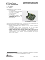
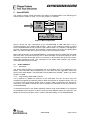
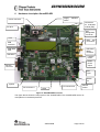
CC1110/CC2430/CC2510
CC1110DK
CC2430DK
CC2510DK
Development Kit
User Manual
Rev. 1.7
SWRU039B
Page 1 of 28
CC1110/CC2430/CC2510
Table of contents
1
2
3
4
4.1
5
5.1
INTRODUCTION ......................................................................................................................3
ABOUT THIS MANUAL ..........................................................................................................3
DEFINITIONS............................................................................................................................3
KIT CONTENT ..........................................................................................................................4
HARDWARE ...................................................................................................................................4
SMARTRF04EB .........................................................................................................................5
SILABS USB MCU ........................................................................................................................5
5.1.1
5.1.2
Bootloader............................................................................................................................................................................. 5
Programming Silabs USB controller.................................................................................................................................... 5
USB MCU SIGNAL NAMES ............................................................................................................6
5.2
6
6.1
6.2
6.3
6.4
6.5
6.6
6.7
6.8
6.9
6.10
7
7.1
7.2
7.2.1
7.2.2
HARDWARE DESCRIPTION SMARTRF04EB ...................................................................8
POWERING SMARTRF04EB...........................................................................................................9
USB INTERFACE ..........................................................................................................................10
RS-232 INTERFACE......................................................................................................................10
USER INTERFACE .........................................................................................................................10
AUDIO INTERFACE .......................................................................................................................10
SPI INTERFACE SWAP JUMPERS ON SMARTRF04EB ....................................................................10
I/O CONNECTORS .........................................................................................................................11
EM CONNECTORS ........................................................................................................................12
SIGNAL FLOW ..............................................................................................................................12
EM LCD CONNECTION ................................................................................................................12
SMARTRF04DK APPLICATION EXAMPLES...................................................................14
SETUP ..........................................................................................................................................14
EXAMPLES ...................................................................................................................................14
7.3.1
7.3.2
RF_TEST ............................................................................................................................................................................. 15
UART Setup......................................................................................................................................................................... 16
RF TESTING .................................................................................................................................16
Output power testing........................................................................................................................................................... 17
Sensitivity testing................................................................................................................................................................. 17
8
8.1
8.2
9
10
11
12
USING SMARTRF04EB FOR PROTOTYPING..................................................................18
USING SMARTRF04EB AS AN IN-CIRCUIT EMULATOR (ICE)......................................................18
DEBUG INTERFACE ......................................................................................................................18
PROGRAMMING THE SOC WITH A HEX FILE .............................................................20
SMARTRF04DK SCHEMATICS...........................................................................................21
EVALUATION MODULES ....................................................................................................28
DOCUMENT HISTORY .........................................................................................................28
7.3
SWRU039B
Page 2 of 28
CC1110/CC2430/CC2510
1
Introduction
Thank you for purchasing a SmartRF®04DK Development Kit.
Please note that Texas Instruments uses the term SmartRF®04DK as a collective term for all
development kits on the Chipcon SmartRF®04 platform. This development platform supports
evaluation, development and prototyping using the Chipcon SmartRF®04 products from
Texas Instruments.
Make sure to subscribe to the Low-Power RF eNewsletter to receive information about
updates to documentation, new product releases and more. Sign up on the Texas
Instruments RF/IF Components web site.
2
About this manual
This manual contains both tutorial and reference information, and covers both the hardware
and software components of the development kit.
Further background information can be found in the SmartRF® Studio User Manual and the
device datasheets.
3
Definitions
SmartRF04EB
SmartRF®04DK
CC2430EM
CC2510EM
CC1110EM
USB MCU
Factory firmware
PER
SoC
ICE
Evaluation Board. Main board with LCD, USB interface, LEDs, potmeter etc. Platform for the Evaluation Modules (EM, see below).
A collective term used for all development kits for the SmartRF®04
platform, i.e. SmartRF04EB + EM.
CC2430 Evaluation Module, a small plug-in module for
SmartRF04DK, should be used as reference design for RF layout.
CC2510 Evaluation Module, a small plug-in module for
SmartRF04DK, should be used as reference design for RF layout.
CC1110 Evaluation Module, a small plug-in module for
SmartRF04DK, should be used as reference design for RF layout.
The Silicon Labs C8051F320 MCU used to provide a USB interface
on the SmartRF04DK.
The firmware that is supplied programmed into the USB MCU from
the factory. This firmware supports SmartRF® Studio operation as well
as a stand-alone PER tester.
Packet Error Rate. Counts the number of lost and/or faulty packets
and displays the ratio: (lost/faulty packets)/number of packets sent.
System on a Chip. A collective term used to refer to Texas
Instruments ICs with on-chip MCU and RF transceiver. Used in this
document to reference the CC2430 and the CC2510.
In Circuit Emulator.
SWRU039B
Page 3 of 28
CC1110/CC2430/CC2510
4
Kit content
4.1
Hardware
The development kit contains the following:
•
•
•
•
•
•
2 x SmartRF04EB
2 x evaluation modules (CC2430EM,
CC1110EM1 or CC2510EM)
2 x 2.4GHz Antennas
2 x USB cables
1 x 10-wire flat cable for using
SmartRF04EB as emulator for
external target systems
Quick start guide
SmartRF04EB with CC2430EM
The SmartRF04DK Development Kit includes a number of functions and applications that
allows quick testing of the RF interface and peripherals of the chip.
•
•
•
Evaluate the SmartRF®04 products. Right out of the box, the kit can be used for
range testing.
Use SmartRF® Studio to perform RF measurements. The radio can be easily
configured to measure sensitivity, output power and other RF parameters.
Prototype development. The SmartRF04DK includes a USB interface that can be
used as emulator interface for the CC1110/CC2430/CC2510. All I/O ports are
available on pin connectors on the edge of the board to allow easy access for
external applications. These connectors are also compatible with logic analyser
probes for easy debugging.
1
The CC1110DK development kit is temporarily changed. Please see the Product Information
section on the CC1110-xxx MHz Development Kit web page for details
SWRU039B
Page 4 of 28
CC1110/CC2430/CC2510
5
SmartRF04EB
This chapter includes overall information that applies to SmartRF04EB. In the following SoC
means Chipcon System on Chip, i.e. CC1100, CC2510, or CC2430.
Figure 1: Main components
Figure 1 shows the main components on the SmartRF04EB. A USB cable from a PC is
connected directly to the Silabs USB controller. When a SoC evaluation module is pulged
into the SmartRF04EB, the only purpose of the USB controller is to “translate” USB signals to
the SoC 2-wire debug interface. This interface includes Debug Clock (DC) and Debug Data
(DD). The USB controller also controls the reset_n line connected to the SoC.
Most of the peripherals on the SmartRF04EB are connected to both the Silabs USB controller
and to the SoC. This means that I/O ports on both controllers can drive the same pin. When
the Silabs controller detects that a SoC is connected, it will therefore set all the I/O in threestate (high impedance) mode. The connection to the Silabs USB controller may anyhow
somewhat influence these I/O lines.
5.1
5.1.1
Silabs USB MCU
Bootloader
The Silabs USB controller is programmed with a bootloader when it is shipped from the
factory. The bootloader allows programming of new code into the USB MCU without the
Silicon Labs’ serial adapter. The bootloader communicates with SmartRF® Studio or a custom
program via USB.
5.1.2
Programming Silabs USB controller
If it is required to update the firmware of the USB MCU, this can be done using the
SmartRF04 programming software (Chipcon Flash Programmer or SmartRF Studio). For use
of Chipcon Flash Programmer please refer to Chipcon Flash Programmer user manual for
instructions. The Silabs controller can only be updated via USB when no EM is connected to
the SmartRF04EB.
To download firmware to the Silabs USB MCU without using the bootloader or to download
the bootloader in the first place, a Silicon Labs’ EC2 serial adapter (Figure 2) is required. This
adapter should be connected to P301, marked “USB MCU debug”, on the SmartRF04EB.
SWRU039B
Page 5 of 28
CC1110/CC2430/CC2510
Figure 2: EC2 serial adapter
5.2
USB MCU signal names
The USB MCU is a C8051F320 from Silicon Labs. Please see the Silicon Labs web site for
detailed information about this MCU.
The following table shows the usage of I/O pins on the USB MCU.
Pin
no.
1
Pin name
(USB MCU)
P0.1
Signal name
SmartRF04EB
P1.7/SO/GDO1/MISO
0-ohm
resistor
R117
2
10
11
12
13
14
15
P0.0
P3.0/C2D
P2.7
P2.6
P2.5
P2.4
P2.3
P1.5/SCLK
R115
P1.3/LED3
P0.4/RTS
RS232_POWER
P2.0/LED_4
RESET_N
R113
R100
16
P2.2
SOC_PRESENT
17
P2.1
P0.6/JOY
R106
18
19
20
21
22
23
24
25
26
27
P2.0
P1.7
P1.6
P1.5
P1.4
P1.3
P1.2
P1.1
P1.0
P0.7
P1.2/LED2
P1.0/LED1
P0.7/POT
P0.5/JOY_PUSH
P1.1/PWM_OUTPUT
P0.1/BUTTON_PUSH
P0.0/MIC_INPUT
P2.4/SCL
P2.3/SDA
P2.2/GDO2/DC
R111
R110
R107
R112
R105
R101
R104
R124
R123
R122
28
P0.6/CNVSTR
P2.1/GDO1/DD
R121
29
30
31
32
P0.5
P0.4
P0.3/XTAL2
P0.2/XTAL1
P0.2/UART_RD
P0.3/UART_TD
P1.4/CSn/SS
P1.6/MOSI
R102
R103
R114
R116
R120
Function
SPI MISO signal,
transceiver/transmitter SO/GDO2
SPI Serial clock
USB MCU Debug pin
LED3 (yellow), active low
Turns RS-232 level converter on/off
LED4 (Blue), active low
LCD Power on reset signal, SoC
RESET
Tells USB MCU whether a SoC is
present.
0 = transmitter/transceiver
1 = SoC
Joystick input (analogue coded
voltage)
LED2 (Red), active low
LED1, (Green), active low
Potentiometer input
Joystick pushed
PWM audio output
Button pushed
Audio input
I2S clock (for LCD)
I2S data (for LCD)
Transceiver/transmitter GDO3, SoC
debug signal
Transceiver/transmitter GDO1, SoC
debug signal
UART RD
UART TD
SPI slave select signal
SPI MOSI signal,
Transceiver/Transmitter SI
Table 1: USB MCU pin-out
SWRU039B
Page 6 of 28
CC1110/CC2430/CC2510
As mentioned in the table, the joystick output is coded as an analogue voltage. This has been
done in order to save the number of pins required on the MCU to interface with the joystick.
The SoC software libraries contain functions to decode the ADC values and indicate in what
direction the joystick is moved. The push function of the joystick is treated as a separate
digital signal.
SWRU039B
Page 7 of 28
CC1110/CC2430/CC2510
6
Hardware description SmartRF04EB
Supply
switch
Power connector
selection
Connectors
for evaluation
module (EM)
DC jack
SoC
debug/flash
connector
LCD
SMA test
connectors
USB
connector
USB MCU
reset
USB MCU
debug
connector
USB MCU
Potentio
meter
Headphone
output
RS-232
connector
Mic.
input
Button
S1
Joystick
I/O connector A
I/O connector B
LEDs
Volume
control
Figure 3: SmartRF04DK overview
The figure above shows the major parts of the SmartRF04EB. The SmartRF04EB serves as
main platform in the development kit.
SWRU039B
Page 8 of 28
CC1110/CC2430/CC2510
6.1
Powering SmartRF04EB
If several power sources are connected to SmartRF04EB the board will be powered from the
supply that supplies the highest voltage.
Figure 4: Power switch setting
The Power Switch S3 must be set according to what power source is used. If 3.3V is applied
using the power terminal block, the switch should be set to the left position. In all other cases,
the switch should be set to the right position for power to be applied to the SmartRF04EB.
This switch can be used to turn off the SmartRF04EB by switching it to the opposite position
of that used to turn it on.
Figure 5: Power connector
The 4-10V input is used for powering the SmartRF04EB using the on-board voltage regulator.
0V is the ground connection. The 3.3V terminal is used for powering the SmartRF04EB,
bypassing the on-board voltage regulator. A voltage between 2.7 and 3.6V can be used when
USB is not active, when using USB the voltage should be limited to 3.0-3.6V.
The SmartRF04EB can be powered in several different ways:
• DC jack connector with standard DC jack power connectors with a 2.5mm centre pin. The
centre pin is used for the positive voltage. A 4-10V DC power supply should be used. The
onboard voltage regulator supplies 3.3V to the board.
• Laboratory power supply. Ground should be connected to the 0V terminal on the power
connector (see Figure 5). A 4-10V supply can be connected to the “4-10V” terminal, or a
3.3V supply can be connected to the “3.3V” terminal (the on-board voltage regulators will
be bypassed in this case). If a 3.3V supply is used, the supply selection switch should be
set to the “3V” position, otherwise the “4-10V” position should be used. If the “4-10V”
position is selected, a voltage regulator supplies the circuitry on the SmartRF04EB;
otherwise the 3.3V supply is applied directly to the SmartRF04EB.
• USB power. If the SmartRF04EB is connected to a USB socket on a PC, it will draw
power from the USB bus. The onboard voltage regulator supplies 3.3V to the board.
• Battery power. The evaluation board includes a 9V-type battery connector on the bottom
side of the PCB. A 9V battery or a battery pack that uses a 9V-type connector can be
SWRU039B
Page 9 of 28
CC1110/CC2430/CC2510
connected to this battery connector. The onboard voltage regulator supplies 3.3V to the
board.
Please note that while the SmartRF04 devices have a wide supply range, the components on
the SmartRF04EB limit the total voltage supply range to 2.7V – 3.6V (3.0V – 3.6V while the
USB is active). The SmartRF04EB has been designed for a temperature range of –40°C to
+85°C (excluding the LCD display). The EM is designed for a temperature range of -40°C to
+85°C.
6.2
USB Interface
The USB interface is used to interface to a PC to run SmartRF® Studio and for programming
and debugging using the PC debugging tools and programmers. If SmartRF® Studio connects
to the SmartRF04EB and detects an old version of the USB MCU firmware, the USB MCU will
be upgraded via this interface. The SmartRF04EB can be bus-powered from the USB
interface.
6.3
RS-232 interface
The RS-232 can be used by custom applications for communication with other devices. The
RS-232 interface utilises a voltage translation device so that the RS-232 port is compatible
with bipolar RS-232 levels.
Note that this RS-232 level converter contains a charge-pump power supply that generates
electric noise.
6.4
User interface
The SmartRF04EB includes a joystick and a push button as user input devices, and four
LEDs and a 2x16 character LCD display as user output devices. The display and user
interface is by default controlled by the factory firmware in the SoC.
6.5
Audio interface
The SmartRF04EB includes a microphone input and headphone output.
The audio output section consists of a volume control, followed by a 4th order Chebychev
filter. This filter serves to attenuate frequencies above 6 kHz, and so converts the PWM signal
to an analogue audio signal. A headphone amplifier IC (TPA4411 from Texas Instruments) is
used to drive the headphones.
Note that the headphone amplifier IC uses switch-mode power supply techniques to generate
negative voltages, and this may cause electrical noise. The headphone amplifier can be
disabled by driving a pin on the USB MCU low (the same pin is used to disable the RS-232
voltage converter).
The audio input section consists of a microphone amplifier that also includes a low-pass antialiasing filter.
A standard PC-type headset with separate microphone and headphone mini-jacks can be
connected directly to the audio interface.
6.6
SPI interface swap jumpers on SmartRF04EB
Due to a bug in early revisions of some of the SoC’s, the MISO and MOSI pins changed
directions when switching between SPI slave and master modes. For newer revisions of the
chip, the SPI jumper should always be in master mode position. The default settings of the
jumpers are SPI master mode, see Figure 6. SPI slave mode is used by the Chipcon packet
sniffer.
SWRU039B
Page 10 of 28
CC1110/CC2430/CC2510
Figure 6: SPI jumper, Master mode
6.7
Figure 7: SPI jumper, Slave Mode
I/O connectors
The I/O connectors bring out all the signals from the EM connectors. These connectors are
compatible with Agilent logic analyser probes. The connectors allow easy access to I/O
signals and to connect prototyping boards.
Pin
1
2
3
4
5
6
7
8
9
10
11
12
13
14
15
16
17
18
19
20
Function
N/C
N/C
P0_0/MIC_IN
VDD
VDD
N/C
P0_1/BUTTON_PUSH
N/C
P0_2/UART_RD
N/C
P0_3/UART_TD
N/C
P0_4/RTS
N/C
P0_5/JOY_PUSH
N/C
P0_6/JOY
N/C
P0_7/POT
GND
Pin
1
2
3
4
5
6
7
8
9
10
11
12
13
14
15
16
17
18
19
20
Table 2: I/O connector A (P10) pin-out
Function
N/C
N/C
VDD
P2_0*/LED4
P1_0/LED1
P2_1/DD
P1_1/PWM_OUTPUT
P2_2/DC
P1_2*/LED2
P2_3*/SDA
P1_3/LED3
P2_4*/SCL
P1_4/CSn
N/C
P1_5/SCLK
RESET_N
P1_6/MOSI
Debug Data Direction(DD_DIR)
P1_7/MISO
GND
Table 3: I/O connector B (P11) pin-out,
* see chapter 6.10.
SWRU039B
Page 11 of 28
CC1110/CC2430/CC2510
6.8
EM connectors
The EM connectors are used for connecting the EM to the SmartRF04EB. The connectors P1
and P2 are used as the main interface.
The EM should be used as an RF reference design with the Chipcon SoC, decoupling, and all
required RF circuitry. It is recommended to copy this reference design when designing
applications with Chipcon RF devices in order to achieve best RF performance.
Note that while it is physically possible to plug an EM not belonging to the SmartRF®04
product range into the SmartRF04EB, the factory firmware and SmartRF® Studio do not
support the use of older devices. The SmartRF04EB can be used with custom firmware for
prototyping using older Chipcon RF devices.
6.9
Signal flow
Figure 8: Evaluation Board Signal flow
The signal lines from the EM connectors run via 0-ohm resistors to the USB MCU and the
various peripherals on the SmartRF04EB. This allows connecting an EM module to other
applications. The USB MCU can be disconnected from the signal pins by removing the 0-ohm
resistors. The I/O connectors are located on the “outside” of the 0-ohm resistors, so they are
still connected to the EM connectors even if the 0-ohm resistors are removed. Please refer to
Table 1 on page 6 for a list of 0-ohm resistors and corresponding signals.
The SmartRF04EB may not work with In-Circuit Emulator (ICE), SmartRF® Studio or the SW
examples when the 0-ohm resistors are removed.
6.10 EM LCD connection
I/O pins P2_3 and 2_4 on the SoC are connected to a 32 kHz X-oscillator on the EM board.
The LCD display is therefore internally, on the EM, swapped from P1_2 to P2_3 and P2_0 to
P2_4 as shown in Figure 9. The figure shows the CC2430EM, but this also applies to both the
CC1110EM and the CC2510EM.
SWRU039B
Page 12 of 28
CC1110/CC2430/CC2510
Figure 9: EM LCD connection
SWRU039B
Page 13 of 28
CC1110/CC2430/CC2510
7
SmartRF04DK application examples
This section describes the application examples available for the CC1110, CC2510 and
CC2430. All examples provide valuable information about setup and usage of different
modules. The examples will be available both as source code and ready-to-upload .hex files
from the Texas Instruments website.
The application examples use a menu system controlled by the joystick. Scrolling through the
examples is performed by moving the joystick up or down, while selecting an example to be
run is done by moving the joystick to the right. Move the joystick to the left to return from an
example. As some examples are run at full speed, it might be necessary to hold the joystick
to the left for a little while to return from the example.
7.1
Setup
1. Plug two Evaluation Modules into the two Evaluation Boards.
2. Connect antennas to both EM boards
3. Apply power to the Development Kits. See chapter 6.1 for more information about
various ways of powering the Development Kit.
4. Turn on power by setting the power switch correctly.
For a more detailed explanation, see the “Quick Start Instructions” for the development kit in
question.
The RS232/UART port is employed in some of the examples. The HyperTerminal setup is
shown in chapter 7.2.2.
7.2
Examples
RF Test
Demonstrates use of the radio. Includes single, continuous, pingpong and packet error rate (PER) mode. These examples are
described further in section 7.2.1.
ADC
This example sets up single ADC sampling from the pot-meter. The
acquired value is scaled to the corresponding voltage and presented
on the LCD along with the decimal value. In addition, the joystick is
sampled and the corresponding direction is presented with an arrow
on the LCD.
ADC Series
This example sets up continuous ADC sampling of the pot-meter.
Timer 1 triggers sampling. A DMA channel is set up to transfer data
from the ADC. The converted values are scaled and used to present
the pot-meter voltage versus time on the LCD.
Temp Sensor
The internal temperature sensor is read by the ADC and an average
value is presented on the LCD.
Stop Watch
Uses timer 3 and the button to form a stopwatch. Push the button to
start, push again to stop and a third time to reset the stopwatch.
Timer 3 is set up to generate interrupts each m-second. These
interrupts are used to increment time. The time is printed
continuously on the LCD.
UART <--> LCD
Data written in HyperTerminal is sent to the SoC via the UART
interface. The received data is printed on the LCD. When Enter is
pressed, the data is returned to HyperTerminal.
SWRU039B
Page 14 of 28
CC1110/CC2430/CC2510
Clock Modes
Demonstrates switching of the main clock source to either the
internal RC-oscillator or the external crystal oscillator. A led is blinked
according to the frequency of the oscillator currently used.
Random Sequence
The random generator is seeded with random sequence. Then, each
time a new random value is needed, the random generator is
clocked. In this process, the data is changed through a linear
feedback shift operation. The data generated is printed on the LCD.
AES (Crypto)
Demonstrates the setup and use of the AES encryption / decryption
module. Involves loading of key and initialisation vector, and utilises
both the CPU and DMA for transferring data to and from the AES
module.
Flash Writing
Demonstrates how to write to flash using a writing-routine located in
RAM or by using DMA. Data is written using the UART. If enter is
pressed, the input is written to flash. The previously written data is
always displayed both in HyperTerminal and on the LCD at example
start-up.
DMA
Direct Memory Access (DMA). A test string is moved from one
location in ram to another using a DMA channel for data transfer.
For other examples on DMA usage see “Flash Writing”, “AES” or
“ADC Series” examples.
Power Modes
Demonstrates how to enter and leave different power modes. Uses
both sleep timer and external interrupt to wake up.
Timer Interrupts
Demonstrate how to set up and execute interrupts from 3 timers on
CC1110/CC2430/CC2510. Each timer is represented on the LCD,
i.e. timer 1 => T1. Beside the symbols of the timers, asterisks blink in
accordance with timer timeouts.
External Interrupt
Demonstrates how to set up external interrupt from the push-button
(S1).
7.2.1
RF_TEST
This example demonstrates the use of the radio through the Simple Packet Protocol (SPP),
which provides an effective radio protocol with address recognition, acknowledgement,
retransmission and CRC check. The SPP is interfaced through the radio functions in this
example.
At start-up, determine for each node which is to be sender (master) and which is to be
receiver (slave). Make sure to have one of each. The receiver will continuously be in receive,
unless when replying / ACK’ing incoming packets.
If the default setting does not work due to heavy traffic from other nodes, it is possible to
change frequency and node addresses in the start-up menu of this example.
The sender may be set to any of the following modes:
Single mode
Each time the joystick is moved to the right, a packet is sent. If the packet is ACK’ed, “OK” is
displayed on the LCD. If the packet is not ACK’ed, the packet is retransmitted a number of
times until either an ACK received, or the remote node is set as unreachable. If the latter is
the case, “failed…” is displayed.
Continuous mode
SWRU039B
Page 15 of 28
CC1110/CC2430/CC2510
Same as single mode, but the transfer is started automatically and not each time the joystick
is moved to the right.
Ping-Pong mode
Transfers a packet to the remote node. The remote node transfers the packet back. The LCD
displays a “ball” which is transferred between the units.
PER test mode
In this mode, the remote unit is asked to transfer 1000 packets. The local node counts the
number of received packets. The packet error rate (PER, ratio of lost packets to the number
of sent packets) is displayed on the LCD. A PER of 0% means that no packets were lost.
7.2.2
UART Setup
To use the UART, open “HyperTerminal” (found under: Start -> Programs -> Accessories ->
Communications -> HyperTerminal). Use the following setting:
Figure 10: COM Properties
Connect an RS232 cable to the PC and the SmartRF04 EB board.
A guide to using the menu system can also be found on the Quick Start Instruction sheet that
is included in the box of the development kit.
7.3
RF testing
RF testing is best performed by using SmartRF® Studio together with the Development Kit.
Connect the SmartRF04DK to a PC using the USB interface. Start the SmartRF® Studio and
select the SmartRF®04 tab. Select the correct Development Kit (several Development Kits
can be connected to a PC at once), it should be listed as “CC2430 – new device”, “CC2510 –
new device” or “CC1110 – new device”, and click the Start button. In the main SmartRF®
Studio window settings can be changed, tests performed and registers adjusted. RF
measurement equipment may be connected to the SMA connector on the EM.
Please see the SmartRF® Studio documentation for more information about the operation of
SmartRF® Studio.
SWRU039B
Page 16 of 28
CC1110/CC2430/CC2510
7.3.1
Output power testing
EB+EM
RF carrier
Spectrum analyser
Figure 11: Output power measurement set up
Plug an EM into the SmartRF04DK, and connect the Development Kit to a PC using USB.
Start SmartRF® Studio. Connect the antenna port of the EM board to a spectrum analyser
using a 50-ohm RF coaxial cable. Use the simple TX function in SmartRF® Studio to set up
the RF chip to emit a carrier at the desired frequency. An accurate measure of the output
power can now be made. It is recommended to use a resolution bandwidth (RBW) of 3 MHz
to ensure that all the RF energy is included in the measurement. Using good-quality RF
cabling, the loss in the cabling should be negligible. However make sure that the spectrum
analyser is calibrated. If possible, check it against a calibrated instrument such as an RF
signal generator. Uncalibrated spectrum analysers can display errors of several dB.
7.3.2
Sensitivity testing
BER tester
PN sequence
RF signal
generator
RF signal
EB+EM
Received data+clock
Figure 12: Sensitivity measurement set up
For proper sensitivity testing, a bit-error rate tester is needed. The exact setup will depend on
the specific make of tester you are using, but in general the setup is as follows:
• The BER tester generates a pseudo-random baseband signal. This is used to
modulate an RF signal generator (in some cases this is integrated in the BER tester).
The modulated RF signal is then fed into the antenna connector of the EM.
• The RF chip should be configured to operate in non-buffered mode, outputting the
received bit stream on the general I/O pins that are routed to the DTEST1 and
DTEST2 SMA connectors on the Evaluation Board.
• The demodulated signal and clock are then fed back to the BER tester. The BER
tester compares this signal with the original pseudo-random baseband signal.
The BER tester will display the number of errors measured in a scientific (e.g. 5E-6) format.
Usually sensitivity is measured for a BER of 1E-3, but it is possible to use other criteria as
well. Normally the RF power from the RF generator is decreased until the BER equals 1E-3.
The RF power delivered by the RF signal generator at this point is the sensitivity figure.
SWRU039B
Page 17 of 28
CC1110/CC2430/CC2510
8
Using SmartRF04EB for prototyping
SmartRF04EB includes a debug and programming interface. The debug interface is
controlled by 2 communication pins. On the SmartRF04EB the interface is controlled by the
USB MCU. This allows both programming and an emulator interface using the USB port.
Table 1 on page 6 shows which pins on the MCU that are used for various peripheral
functions. P10 and P11 pin-row connectors can be used to connect the SmartRF04EB to
another PCB or prototyping board.
8.1
Using SmartRF04EB as an In-Circuit Emulator (ICE)
The SmartRF04EB can be used as ICE both for devices connected to the EM socket and for
external systems with custom applications. Figure 13 shows the main components on
SmartRF04EB when it’s used as ICE. Please notice that if the SmartRF04EB is used to
debug an external system, the EM shall be removed, and vice versa.
Figure 13: SmartRF04EB used as ICE
If several SmartRF04EB boards are connected to the PC’s USB ports simultaneously a
selection window will display the connected SmartRF04EBs, and the user can select which
device to load. This is valid for all Chipcon PC software.
8.2
Debug interface
When designing applications with Chipcon SoC’s it is recommended to include a pin header
or test points to allow in-circuit emulation or programming using SmartRF04EB or other
programming tools.
The pin-out used on the SmartRF04EB is explained in Table 4. The connector includes 4 SPI
control signals. These are currently not used, but they are included for flexibility.
The SmartRF04EB includes a voltage converter to support programming and debugging of
external systems with different operating voltage than the SmartRF04EB. The debug
connector (P14, “SoC debug/ flash”) includes two VDD connections on pin 2 and pin 9. The
function is different for these connections.
Pin 2 VDD supplies voltage to the voltage converter. This pin should be connected to VDD,
on the external board to assure that the correct supply voltage is used for the voltage
converter. This pin must always be connected. The voltage on the target system must be
above 2.7 V when debugged from SmartRF04EB.
Pin 9 VDD supplies VDD (3.3 V) from the SmartRF04EB. If the target application is powered
from the SmartRF04EB supply during programming and debugging this pin should be
connected. If the target voltage differs from 3.3V, this pin should not be connected.
SWRU039B
Page 18 of 28
CC1110/CC2430/CC2510
The pin out used on the SmartRF04EB is explained in Table 4 and Figure 14. All signals in
bold in the table are required. Figure 14 shows the required signals for a minimum connector
layout.
Pin
1
2
Function
GND
VDD
3
4
5
6
7
8
9
10
Debug Clock (DC)
Debug Data (DD)
CSn
SCLK
Reset_N
MOSI
3.3V VDD, alt. NC
MISO
Note
Used to set correct voltage for the
voltage level converter
Delivers VDD from SmartRF04EB
Table 4: P14 SoC debug connector pin-out
1
2
1. GND
2. VDD
3. DC
4. DD
7. Reset_N
Figure 14: Recommended debug connector layout (Top view)
SWRU039B
Page 19 of 28
CC1110/CC2430/CC2510
9
Programming the SoC with a HEX file
The SoC can be programmed from the USB interface using the Chipcon programming
software. Figure 15 shows the user interface of the Chipcon Flash Programmer. For
additional information regarding the Chipcon Flash Programmer please refer to the Chipcon
Flash Programmer User Manual.
Figure 15: Chipcon Flash programmer software
SWRU039B
Page 20 of 28
CC1110/CC2430/CC2510
10 SmartRF04DK Schematics
Figure 16: SmartRF04EB schematic, page 1
SWRU039B
Page 21 of 28
CC1110/CC2430/CC2510
Figure 17: SmartRF04EB schematic, page 2
SWRU039B
Page 22 of 28
CC1110/CC2430/CC2510
Figure 18: SmartRF04EB schematic, page 3
SWRU039B
Page 23 of 28
CC1110/CC2430/CC2510
Figure 19: SmartRF04EB schematic, page 4
SWRU039B
Page 24 of 28
CC1110/CC2430/CC2510
Figure 20: SmartRF04EB schematic, page 5
SWRU039B
Page 25 of 28
CC1110/CC2430/CC2510
Figure 21: SmartRF04EB schematic, page 6
SWRU039B
Page 26 of 28
CC1110/CC2430/CC2510
Figure 22: SmartRF04EB schematic, page 7
Revision
1.9 (PCB 1.9)
Description/Changes
Initial public release
Table 5: SmartRF04EB change list
SWRU039B
Page 27 of 28
CC1110/CC2430/CC2510
11 Evaluation Modules
Gerber files and full documentation for the released evaluation modules can be downloaded
from the Texas Instruments web site.
Figure 23: Evaluation Module
12 Document history
Revision
Date
1.7
2006-10-12
1.6
1.5
1.4
1.3
1.2.1
1.2
1.1
1.0
2006-06-01
2006-02-16
2006-02-06
2006-01-25
2006-01-19
2006-01-10
2005-12-28
2005-12-16
Description/Changes
Major updates in many part of the document including
Table 1: typo, R101 changed to 117, Table 3 P2_0/DC changed to P2_2/DC,
removed all EM schematics since the most recent versions are available on web.
Minor changes
Changed layout, changed P0_4/CTS to P0_4/RTS in table “USB MCU pin-out”
Updated to include CC1110
Added temperature sensor to examples
Minor corrections
Updated schematics and minor corrections
Updated to include CC2510
Initial release
SWRU039B
Page 28 of 28