1
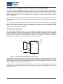
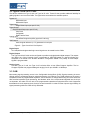
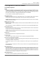
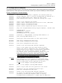
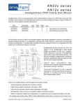
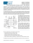
AN13x series
AN23x series
AnadigmApex dpASP Family User Manual
AnadigmApex represents the third generation of dynamically programmable Analog Signal Processor
(dpASP) devices from Anadigm. Two members of the AnadigmApex family are currently shipping providing
access to the latest in programmable analog technology: AN131E04 and AN231E04. Both of these devices
provide 7 analog I/O Cells and 4 Configurable Analog Blocks (CABs).
IO Cell 7
(Type 2a)
Chopper
Amplifier
Support
IO Cell 6
(Type 2)
IO Cell 5
(Type 2)
SCLK
ACLK
IO5N
IO5P
IO6N
IO6P
IO7N
IO7P
This third generation dpASP delivers improved analog performance and increased value. The configuration
interface of the AN23x devices is enhanced to accommodate dynamic reconfiguration - a breakthrough
capability that allows analog circuit functionality to be controlled by a companion host processor.
Clock
Generation
Bi-Directional Switch Fabric
Connects any CAB to any Input / Output Cell
Analog
MODE
Logic
0 1 2 3 4 5
I2N
O2P
IO Cell 2
(Type 1)
I2P
O2N
O1P
IO Cell 1
(Type 1)
I1P
I1N
CAB3
CAB4
Configuration RAM
Shadow RAM
CAB2
CS1b
CS2b
Configuration Interface
O3N
CAB1
Configuration RAM
Shadow RAM
O3P
IO Cell 3
(Type 1a)
I3P
I3N
Shadow RAM
Configuration RAM
O4N
Shadow RAM
Configuration RAM
O4P
Bi-Directional Switch Fabric
Connects any CAB to any Input / Output Cell
I4N
IO Cell 4
(Type 1a)
I4P
SI
CFGFLGb
ACTIVATE
ERRb
RESETb
SO
MEMCLK
LCCb
O1N
VREF+
VMR
VREF-
Look-Up Table
BVSS
VREFN
VMR
VREFP
Voltage Refrences
BVDD
DVSS
AVSS
DVDD
AVDD
Power & Gnd
•
Faster time-to-solution compared to discretes or ASICs
•
High precision operation despite system degradation and aging
•
Eliminates the need to source and maintain multiple inventories of product
•
Ability to implement multiple chip configurations in a single device and to adapt functionality in the field
The Anadigmvortex solution allows OEMs to deliver differentiated solutions faster and at lower overall system cost.
Copyright © 2006 Anadigm, Inc., All Rights Reserved
UM000231-U001e
Legal Notice
Anadigm reserves the right to make any changes without further notice to any products herein. Anadigm makes
no warranty, representation or guarantee regarding the suitability of its products for any particular purpose, nor
does Anadigm assume any liability arising out of the application or use of any product or circuit, and specifically
disclaims any and all liability, including without limitation consequential or incidental damages. "Typical"
parameters can and do vary in different applications. All operating parameters, including "Typicals" must be
validated for each customer application by customer's technical experts. Anadigm does not in this manual
convey any license under its patent rights nor the rights of others. Anadigm software and associated products
cannot be used except strictly in accordance with an Anadigm software license. The terms of the appropriate
Anadigm software license shall prevail over the above terms to the extent of any inconsistency.
Copyright © 2005 Anadigm, Inc.
All Rights Reserved
Anadigm, and AnadigmDesigner, are registered trademarks of Anadigm, Inc.
The Anadigm logo is a trademark of Anadigm, Inc.
Copyright © 2006 Anadigm, Inc., All Rights Reserved
UM000231-U001e
Ta b l e o f C o n t e n t s
1 Architecture Overview
1
Using a dynamically programmable Analog Signal Processor ..................................................... 2
2 Typical Configuration Interface Connections
3
2.1 Dynamic Operation ............................................................................................................................... 3
2.2 Static Operation .................................................................................................................................... 4
Pull-Ups on SI .............................................................................................................................. 6
Pull-Ups on ERRb ........................................................................................................................ 6
Pull-Ups on ACTIVATE ................................................................................................................ 6
Pull-Ups on CFGFLGb ................................................................................................................. 6
3 Analog Architecture Details
7
3.1 Types 1 and 1a IO Cells ....................................................................................................................... 7
Bypass.......................................................................................................................................... 7
Digital ........................................................................................................................................... 7
Analog Input ................................................................................................................................. 7
Analog Output .............................................................................................................................. 8
VMR Output.................................................................................................................................. 8
Amplifier Detail - Rauch Filter Designs......................................................................................... 8
3.2 Types 2 and 2a IO Cells ....................................................................................................................... 9
Digital Input .................................................................................................................................. 9
Digital Output................................................................................................................................ 9
Analog Input ................................................................................................................................. 9
3.3 CAB ....................................................................................................................................................... 9
4 Configuration Interface Details
10
4.1 Pin Descriptions .................................................................................................................................. 10
MODE......................................................................................................................................... 10
SCLK (Serial Clock) ................................................................................................................... 10
MEMCLK (Memory Clock).......................................................................................................... 10
ACLK (Analog Clock) ................................................................................................................. 10
SI (Serial In) ............................................................................................................................... 10
SO (Serial Out) ........................................................................................................................... 10
LCCb (Local Configuration Complete) ....................................................................................... 10
CS1b (Chip Select 1).................................................................................................................. 10
CS2b (Chip Select 2).................................................................................................................. 10
CFGFLGb (Configuration Flag) .................................................................................................. 11
ERRb (Error) .............................................................................................................................. 11
ACTIVATE .................................................................................................................................. 11
RESETb ..................................................................................................................................... 11
4.1.1 Secondary Pin Functions ............................................................................................................... 11
4.2 Special Functions - Configuration and Control Features .................................................................... 12
4.2.1 Resets ............................................................................................................................................ 12
4.2.2 ERRb .............................................................................................................................................. 12
4.2.3 Watchdog ....................................................................................................................................... 12
4.2.4 Analog and Configuration Clock Generation .................................................................................. 13
4.3 SRAM .................................................................................................................................................. 14
4.3.1 LUT................................................................................................................................................. 14
4.3.2 Auxiliary Cell (AN23x Only) ............................................................................................................ 14
Immediate................................................................................................................................... 14
Event Driven ............................................................................................................................... 14
Event Driven and Armed ............................................................................................................ 14
Clock Synchronization ................................................................................................................ 14
Copyright © 2006 Anadigm, Inc., All Rights Reserved
i
UM000231-U001e
Ta b l e o f C o n t e n t s
5 Dynamic Operation Details
15
5.1 Configuration Data Stream Protocol ................................................................................................... 15
5.1.1 Primary Configuration Format ........................................................................................................ 15
5.1.2 Header Block .................................................................................................................................. 17
SYNC BYTE ............................................................................................................................... 17
Device ID BYTE ......................................................................................................................... 17
ADDR1 BYTE ............................................................................................................................. 17
5.1.3 Data Block ...................................................................................................................................... 18
CONTROL BYTE ....................................................................................................................... 18
Write ........................................................................................................................................... 18
RESET_ALL ............................................................................................................................... 18
ENDEXECUTE ........................................................................................................................... 18
BYTE ADDRESS BYTE ............................................................................................................. 19
BANK ADDRESS BYTE ............................................................................................................. 19
DATA COUNT BYTE.................................................................................................................. 20
DATA BYTE ............................................................................................................................... 20
DATA BLOCK END BYTE.......................................................................................................... 20
CRC_MSB and CRC_LSB BYTEs ............................................................................................. 20
5.1.4 Update Format (AN23x Only) ......................................................................................................... 21
5.2 Configuration Examples ...................................................................................................................... 22
Primary Configuration Format Example ..................................................................................... 22
Update Format Example (AN23x Only) ...................................................................................... 23
5.3 Advanced Feature - Logical Addressing ............................................................................................. 23
Tieing CFGFLGb Pins Together in multi-dpASP Systems ......................................................... 24
6 Package and Pin Information
25
6.1 Recommended PCB Design Practices ............................................................................................... 27
Copyright © 2006 Anadigm, Inc., All Rights Reserved
ii
UM000231-U001e
Ta b l e o f F i g u r e s
Architecture Overview
Figure 1 – Overview of the AN13x and AN23x dynamically programmable Analog Signal Processor Architecture ................................................................................................................................................................... 1
Typical Configuration Interface Connections
Figure 2 – Configuring a single dpASP from a Host Processor ....................................................................... 3
Figure 3 – Configuring multiple dpASPs from a Host Processor ..................................................................... 4
Figure 4 – A single dpASP self configuring from a SPI PROM ........................................................................ 4
Figure 5 – Multiple dpASPs self configuring from a single SPI PROM ............................................................ 5
Analog Architecture Details
Figure 6 – Types 1 and 1a IO Cell Options ...................................................................................................... 7
Figure 7 – Rauch Input Anti-Aliasing Filter ....................................................................................................... 8
Figure 8 – Rauch Output Smoothing Filter ....................................................................................................... 8
Figure 9 – Types 2 and 2a IO Cell Options ...................................................................................................... 9
Configuration Interface Details
Figure 10 – MODE Controls the Behavior of the Configuration Interface ...................................................... 13
Dynamic Operation Details
Figure 11 – Primary Configuration Data Stream Structure ............................................................................ 16
Figure 12 – Device IDs for the AnadigmApex Family .................................................................................... 17
Figure 13 – AN13x and AN23x Memory Allocation ........................................................................................ 19
Figure 14 – Update Data Stream Structure .................................................................................................... 21
Figure 15 – Primary and Alternate Logical Addressing .................................................................................. 24
Package and Pin Information
Figure 16 – AN13x/AN23x devices are supplied in a standard 44 QFN package .......................................... 25
Figure 17 – Pin Numbering and Descriptions ................................................................................................ 26
Copyright © 2006 Anadigm, Inc., All Rights Reserved
iii
UM000231-U001e
1 Architecture Overview
The AnadigmApex family of dpASPs includes AN13x and the AN23x series devices. These dpASPs process
analog signals in their IO Cells and Configurable Analog Blocks (CABs). These structures are constructed
from a combination of conventional and switched capacitor circuit elements and are programmed from off-chip
non-volatile memory or by a host processor. Programmable analog arrays enable adaptability and flexibility in
analog circuits not previously possible.
The SRAM based AN23x devices are dynamically reconfigurable. The behavior of the dpASP can be modified
partially or completely while operating. Dynamic Reconfiguration allows a companion host processor to send
new configuration data to the dpASP while the old configuration is running. Once the new data load
completes, the transfer to the new analog signal processing configuration happens in a single clock cycle.
Dynamic Reconfiguration in the AN23x device allows the user to develop innovative analog systems that can
be updated (fully or partially) on-the-fly, as often as needed.
IO Cell 7
(Type 2a)
Chopper
Amplifier
Support
IO Cell 6
(Type 2)
IO Cell 5
(Type 2)
SCLK
ACLK
IO5N
IO5P
IO6N
IO6P
IO7N
IO7P
The AN13x devices are also SRAM based and can also be reprogrammed as many times as desired,
however the device must always first be reset before issuing a configuration data set.
Clock
Generation
Bi-Directional Switch Fabric
Connects any CAB to any Input / Output Cell
Analog
MODE
Logic
0 1 2 3 4 5
I2N
O2P
IO Cell 2
(Type 1)
I2P
O2N
I1N
O1P
IO Cell 1
(Type 1)
I1P
CAB3
CAB4
Configuration RAM
Shadow RAM
CAB2
CS1b
CS2b
Configuration Interface
O3N
CAB1
Configuration RAM
Shadow RAM
O3P
IO Cell 3
(Type 1a)
I3P
I3N
Shadow RAM
Configuration RAM
O4N
Shadow RAM
Configuration RAM
Bi-Directional Switch Fabric
Connects any CAB to any Input / Output Cell
I4N
O4P
IO Cell 4
(Type 1a)
I4P
SI
CFGFLGb 1,2
ACTIVATE 1,2
ERRb 1,3
RESETb
SO
MEMCLK
LCCb
O1N
VMR
VREF-
Look-Up Table
1 Open Drain Output
2 Programmable Internal Pull-Up
3 10KW External Pull-Up Required
BVSS
VREFN
VMR
Voltage Refrences
VREFP
DVSS
VREF+
BVDD
AVSS
DVDD
AVDD
Power & Gnd
Figure 1 – Overview of the AN13x and AN23x dynamically programmable Analog Signal Processor
Architecture
AN13x and AN23x dpASPs contain 4 Configurable Analog Blocks (CABs) in their cores. Most of the analog
signal processing occurs within these CABs and is done with fully differential switched capacitor circuitry. The
CABs share access to a single Look Up Table (LUT) which offers a method of adjusting any programmable
Copyright © 2006 Anadigm, Inc., All Rights Reserved
1
UM000231-U001e
AN13x /AN23x
AnadigmApex dpASP Family User Manual
element within the device in response to a signal or time base. The LUT can also be used to implement arbitrary input-to-output transfer functions (companding, sensor linearization), generate arbitrary signals, and
construct voltage dependent filtering. A Voltage Reference Generator supplies reference voltages to each of
the CABs within the device and has external pins for the connection of filtering capacitors.
Analog signals are routed in and out of the dpASP core via the available IO cells: two Type 1, two Type 1a,
two Type 2, and one Type 2a. Type 1 and Type 1a IO cells contain both passive and active circuitry which
allows direct signal input and output, building of active filters, sample and hold circuits, digital inputs, and
digital outputs. The response of continuous time input and output filters is determined by a combination of
internal programming and external components.
Type 2 and Type 2a IO cells are simpler and can implement direct input and output, reference voltage output,
digital input, and digital output.
Any one of the Type 1a or Type 2a IO cells can have access to a specialized chopper amplifier resource which
allows accurate amplification of very low energy inputs signals.
Look-Up Table (LUT) functionality facilitates the construction of arbitrary waveform generators and non-linear
transfer functions. On-chip voltage reference generation precludes the need of any external reference voltage
generation circuitry.
Using a dynamically programmable Analog Signal Processor
The design of circuits for the dpASP is accomplished using AnadigmDesigner2. This software presents a
graphical circuit design environment in which basic analog signal processing building blocks are dropped into
place and wired together. Building blocks include: gain, filter, summing, rectification and many other more
specialized behaviors. Specific parameters for each of the blocks used (e.g. Gain, Corner Frequency, etc.) are
set by the user. AnadigmDesigner2 generates a configuration data file. The dpASP’s configuration data file
can be used to program a SPI PROM for stand-alone static operation, or compiled into a microcontroller’s
source program for hosted dynamic operation.
AnadigmDesigner2 also generates C source code for a host microcontroller which enables on-the-fly generation of new dpASP configuration data and subsequent dynamic reconfiguration. The dpASPs’ signal
processing behavior can be adjusted while your system remains continuously in mission mode.
The behavior of the analog circuitry is controlled by the contents of the dpASP’s configuration memory. This
memory is SRAM based and must be programmed after power-up. The dpASP’s configuration interface
provides a data port for this purpose. The configuration interface presents itself as a slave serial data port to a
companion microprocessor, compatible with SPI signaling. The configuration interface can otherwise be
configured to read data from an attached SPI PROM automatically after power-up or a device reset.
Copyright © 2006 Anadigm, Inc., All Rights Reserved
2
UM000231-U001e
2 Typ ical Configuration Interface Connections
The behavior of the analog signal processing circuits within an AN13x/AN23x device is dictated by the
contents of its volatile (SRAM based) configuration memory. At power-on-reset, the dpASP clears its memory,
placing the device in a benign condition. Once this power-on-reset sequence concludes, the device is ready to
accept configuration data. The first configuration data set loaded into the device after a reset is called a
Primary Configuration.
AN13x devices accept only Primary Configurations. A reset is required before reconfiguring an AN13x device.
AN23X devices on the other hand can be reconfigured (without intervening resets) using the Update format
described later.
The configuration interface presents itself as either a serial data master or serial data slave. As a serial data
master, the dpASP can automatically retrieve its configuration data set from any industry standard SPI PROM
attached. As a serial data slave, the dpASP is compatible with SPI signaling from a host processor and can
accept its configuration data from that host.
2.1 Dynamic Operation
The most powerful application scheme is when the dpASP is configured as a serial data slave. In this
Dynamic Operation a companion host processor sends configuration data to the dpASP using SPI compatible
signaling. This allows the creation of analog signal processing circuits that can be changed on-the-fly. The
change may be as simple as a minor adjustment of a gain or corner frequency, or may involve wholesale
transformation of behavior, say from a transmitter to a receiver configuration.
Host
Processor
MOSI
AN13x/AN23x
10K
RESETb
SI
ACTIVATE
SO
ERRb
MEMCLK
SCLK
SCLK
CFGFLGb
SELb
CS2b
CS1b
<16 MHz
ACLK
LCCb
MODE
Figure 2 – Configuring a single dpASP from a Host Processor
Out of power-on-reset, the dpASP remains in a benign state, waiting for a configuration sequence. In order to
configure the dpASP, the host processor drives CS2b low then streams a configuration data set out of its serial
data port. Normally, the dpASP will enable analog signal processing automatically at the conclusion of configuration, though other options are discussed below.
AN13X devices can be configured any number of times, but an intervening reset is required between each
configuration load. AN23x devices are more flexible, allowing for on-the-fly reconfiguration any number of
times after a reset.
Copyright © 2006 Anadigm, Inc., All Rights Reserved
3
UM000231-U001e
AN13x /AN23x
AnadigmApex dpASP Family User Manual
Host
Processor
MOSI
AN13x/AN23x
AN13x/AN23x
RESETb
SI
ACTIVATE
SO
SELb
ACTIVATE
SO
SI
ACTIVATE
SO
ERRb
MEMCLK
ERRb
MEMCLK
SCLK
SCLK
SCLK
CFGFLGb
CFGFLGb
CFGFLGb
CS2b
CS2b
CS1b
<16 MHz
RESETb
SI
ERRb
MEMCLK
SCLK
AN13x/AN23x
10K
RESETb
ACLK
CS2b
CS1b
LCCb
ACLK
MODE
CS1b
LCCb
ACLK
MODE
LCCb
MODE
Figure 3 – Configuring multiple dpASPs from a Host Processor
Configuring several dpASPs from a Host Processor is a simple matter of busing the serial clock and data
signals to each of the dpASPs. Figure 3, shows the parallel connection of the host’s MOSI, SCLK and select
signals to an arbitrary number of dpASPs.
The LCCb pin of the upstream device is tied to the CS1b pin of the downstream device, holding off downstream configurations until the upstream device gets its configuration. This connection coupled with
CFGFLGb pin behavior and logical addressing described later allows for conservation of host processor slave
device select outputs. Note that the entire chain of dpASPs only requires a single select pin from the host.
ACTIVATE and ERRb nodes are tied together in order to facilitate the concurrent activation of analog circuitry
and provide for configuration error handling. When connecting two or more dpASPs together as shown, it is
important to bus together the CFGFLGb pins.The guidelines for the use of pull-up resistors on these nodes
are given below in section 2.2.
Though not shown above, it is common practice to have the Host Processor monitor the ERRb node.
2.2 Static Operation
In static operation, the dpASP will automatically read in its configuration data from an SPI PROM after a
manual reset or on power-up.
SPI
PROM
AN13x/AN23x
10K
RESETb
MISO
SI
MOSI
SO
SCLK
MEMCLK
ACTIVATE
ERRb
SCLK
SSb
CFGFLGb
CS2b
LCCb
CS1b
<16 MHz
ACLK
MODE
This example assumes internal pull-ups
are enable for ACTIVATE & CFGFLG.
Figure 4 – A single dpASP self configuring from a SPI PROM
Copyright © 2006 Anadigm, Inc., All Rights Reserved
4
UM000231-U001e
At the conclusion of the power-on-reset sequence, CFGFLGb will be low, selecting the attached SPI PROM.
The standard “read” command will be issued out of SO (clocked by MEMCLK). As MEMCLK continues, the
SPI PROM responds with a serial data stream. This serial data stream is read by the SI pin.
Normally, the dpASP will enable analog signal processing automatically at the conclusion of configuration,
though other options are discussed in more detail below.
In this simplest use model, the dpASP automatically: detects power-on, resets itself, reads in configuration
data from a standard SPI PROM, and begins analog signal processing. A subsequent reset or power cycle will
cause the sequence to repeat.
A slightly more advanced application of static configuration allows for the connection of several dpASP’s to a
single SPI PROM. In this use scenario, the dpASPs are daisy chained; the upstream (closer to the PROM)
device’s Local Configuration Complete (LCCb) pin feeds the downstream device’s CS1b enable pin. The SPI
PROM’s MISO data output pin is bused to all dpASPs. All dpASP’s have their ACTIVATE and ERRb pins
commoned.
SPI
EPROM
AN13x/AN23x
10K
PORb
PORb
MISO
SI
MOSI
SO
SCLK
MEMCLK
SSb
AN13x/AN23x
ACTIVATE
SI
ERRb
ERRb
MEMCLK
SCLK
SCLK
CFGFLGb
CFGFLGb
CS2b
CS2b
CS1b
<16 MHz
ACTIVATE
SO
ACLK
LCCb
LCCb
CS1b
ACLK
MODE
MODE
This example assumes internal pull-ups
are enable for ACTIVATE & CFGFLG.
Figure 5 – Multiple dpASPs self configuring from a single SPI PROM
As with the single dpASP example, the first dpASP in the chain still provides the “read” command to the SPI
PROM but provides the necessary clocking for all the serial configuration data. As the configuration completes
for an upstream device, its LCCb asserts low and enables the next device in the chain (downstream) to
receive its data.
ACTIVATE is an open-drain bidirectional pin. During configuration the ACTIVATE pin is asserted low. Analog
circuitry is not enabled (activated) until the ACTIVATE pin moves to a high state. As the local configuration
completes, the dpASP de-asserts its ACTIVATE pin and monitors the ACTIVATE node. The daisy chained
LCCb to CS1b sequence continues until all dpASPs in the chain have received configuration data. At that
point all of the dpASPs will have de-asserted ACTIVATE and the commoned line will pull-high. Tying the
ACTIVATE pin of all the devices in the configuration chain together ensures that analog signal processing
does not begin in any of the dpASPs until all of them have received their configuration data.
ERRb is also an open-drain bidirectional pin. The ERRb pin will assert low if illegal or corrupted data is
detected. Tying the ERRb pin of all the devices in the configuration chain together ensures that if any device
detects an error, then all of the devices in the chain will reset (including the SPI PROM) and the configuration
sequence will re-start automatically.
Copyright © 2006 Anadigm, Inc., All Rights Reserved
5
UM000231-U001e
AN13x /AN23x
AnadigmApex dpASP Family User Manual
Pull-Ups on SI
Most SPI EPROMs hold their MISO pin in tri-state when the device is not selected. In order to ensure a
valid logic signal is always presented to the dpASP a pull-up on the SI node is recommended.
Pull-Ups on ERRb
A 10 KW resistor is always required on the ERRb node.
Pull-Ups on ACTIVATE
The ACTIVATE pin has a programmable internal pull-up. In Master mode systems in which there are 3
or fewer dpASPs, it is recommended that the most upstream device enable its ACTIVATE pull-up.
Master mode systems constructed with 4 or more dpASPs should use only an external pull-up on the
ACTIVATE node.
Pull-Ups on CFGFLGb
The CFGFLGb pin has a programmable internal pull-up. The internal pull-ups for CFGFLGb and
ACTIVATE are controlled with a single configuration bit; they are not separately programmable. Consequently, the same pull-up rules for ACTIVATE apply here to CFGFLGb.
Copyright © 2006 Anadigm, Inc., All Rights Reserved
6
UM000231-U001e
3 Analog Architecture Details
3.1 Types 1 and 1a IO Cells
The device contains two Type 1 and two Type 1a IO cells. These IO sites provide tremendous flexibility in
getting signals in and out of the CABs. The figure below summarizes the available options.
Bypass I/O
Differential Input
Differential Output
Digital I/O
Differential Input
Differential Output
Analog Input
Amplifier, or
Differential Low Offset Chopper Amplifier (type 1a IO cell only), or
Sample and Hold, with options for input:
Differential
Inverted Differential
Single Ended Positive
Single Ended Negative
Analog Output
Differential Amplifier
Differential Sample and Hold
VMR Output
Internal signal reference (1.5 V) presented on both pins.
Figure 6 – Types 1 and 1a IO Cell Options
Bypass
The Bypass setting of the IO cells provides direct, unbuffered access to CAB input and output ports.
When using Bypass inputs, care should be taken to ensure that the differential signal and reference
voltages are compatible with the CAB. Differential voltages should be maintained between 0 and 3 V,
and centered about VMR (1.5 V).
Digital
Differential logic buffers are available to get signals into and out of the array. This IO configuration is
most often used with Comparator and ADC-SAR CAMs.
Analog Input
The Amplifier’s outputs are presented to the external pins for construction of anti-aliasing filters and
external gain control.
The Sample and Hold setting provides a sampling circuit which can be used with either phase of the IO
cell’s clock. The Sample and Hold input can be configured as: Differential, Inverted Differential, Single
Ended Positive, or Single Ended Negative.
On Type 1a IO cells, a Low Offset Chopper Amplifier setting is available. The Chopper Amplifier is specially designed to provide very low offset voltages for weak external signals which must be gained up
prior to processing in the CAMs. This setting includes programmable gain from 0, to 40 dB in 10 dB
steps.
Only a single IO cell in a configuration is allowed access to the shared Chopper Amplifier resources..
Copyright © 2006 Anadigm, Inc., All Rights Reserved
7
UM000231-U001e
AN13x /AN23x
AnadigmApex dpASP Family User Manual
Analog Output
Similar to Analog Input, Analog Output settings include: Amplifier, and Sample and Hold. Signalling
from an Analog Output is always differential. The Amplifier setting of Analog Output is unique in that the
IO cell presents its differential amplifier inputs and outputs to the device pins for external use only.
There are no signals from the core of the device involved. This setting is used for the creation of an
output smoothing filter for a differential analog signal sourced by another IO site.
VMR Output
The VMR Output setting places the device’s internal signal reference (1.5 V) on two pins of the IO site.
Amplifier Detail - Rauch Filter Designs
The Amplifier setting of the Type 1 and 1a IO cells accomodates construction of continuous time input
anti-aliasing and output smoothing filters. Rauch (a.k.a. multiple feedback, MFB) differential filter construction is the recommended topology.
R1
R2
C2
O1P
R3
I1N
-
I1P
+
C1
External Signal Input
to CAB
R3
C2
R1
R2
O1N
Type 1 - IO Cell
Input Amplifier Setting
Figure 7 – Rauch Input Anti-Aliasing Filter
The same filter design technique can also be used in the construction of an output smoothing or reconstruction filter. In this case, the unfiltered output signal is sourced by a Bypass output and the amplifier used to
construct the filter is provided by an adjacent IO cell using its output Amplifier setting.
External Signal Output
R2
O1P
R1
C2
R3
+
I1N
C1
R3
I1P
C2
R2
R1
O1N
Type 1 - IO Cell
Output Amplifier Setting
O2P
from CAB
Any IO Cell
Bypass Setting
O2N
Figure 8 – Rauch Output Smoothing Filter
Copyright © 2006 Anadigm, Inc., All Rights Reserved
8
UM000231-U001e
3.2 Types 2 and 2a IO Cells
The device contains two Type 2 and one Type 2a IO cells. These IO sites provide additional flexibility for
getting signals in and out of the CABs. The figure below summarizes the available options.
Bypass I/O
Differential Input
Differential Output
Digital Input
Single Ended Input (two per IO Cell)
Digital Output
Single Ended Output (two per IO Cell)
Chip Clock
Comparator
RAM Transfer Done
Analog Input
Low Offset Chopper Amplifier (type 2a IO cell only)
VMR Output
Internal signal reference (1.5 V) presented on both pins.
Figure 9 – Types 2 and 2a IO Cell Options
Digital Input
Two independent single ended logic control signals can be routed into the CAMs.
Digital Output
The Type 2 and 2a IO cells can be configured to provide two singled ended digital outputs. The outputs
can reflect: any of the 6 internal clocks, a comparator or ADC-SAR output or a signal indicating the
completion of a transfer from Shadow SRAM to Configuration SRAM. The polarity of these output
signals is programmable.
Analog Input
Like the Type 1a IO cell, the Type 2a IO cell also offers a Low Offset Chopper Amplifier. The 2a
Chopper Amplifier has programmable gain ranging from 0 up to 60 dB in 10 dB steps.
3.3 CAB
Most analog signal processing occurs in the Configurable Analog Block (CAB). Signal processing is accomplished using an architecture based on switched capacitor circuit design. Every CAB contains two op-amps, a
comparator, banks of programmable capacitors, and a collection of configurable routing and clock resources.
With switched capacitor signal processing, the absolute value of the components integrated into the chip is
not important, but rather it is the ratio of the programmable capacitors employed and the clock frequencies
that determine circuit response; both of which are well controlled. In order to further improve signal fidelity, all
signal processing within the CABs is fully differential.
Copyright © 2006 Anadigm, Inc., All Rights Reserved
9
UM000231-U001e
AN13x /AN23x
AnadigmApex dpASP Family User Manual
4 Con figuration Interface Details
4.1 Pin Descriptions
MODE
The state of the MODE pin is read as part of the dpASP’s power-on-reset sequence. If MODE is low out
of reset the configuration interface establishes itself as a serial data slave. If MODE is high, the configuration interface establishes itself as a serial data master. MODE should either be tied high to VDD or
low to VSS. This is a static pin. Changing its state after power up is not allowed.
For more details on the effects of MODE, see section 4.2.4.
SCLK (Serial Clock)
If MODE is low, SCLK serves as the serial data clock input. The configuration state machine is driven
from this input. SCLK may not exceed 40 MHz. SCLK may be free running or discontinuous.
If MODE is high, then SCLK is ignored and the configuration state machine is driven from an internally
divided down ACLK (ACLK/16).
MEMCLK (Memory Clock)
If MODE is high, the dpASP establishes itself as a serial data master. MEMCLK serves as the serial
data clock output.
Once configuration is complete, the MEMCLK pin may be used as a user programmable digital output.
ACLK (Analog Clock)
ACLK is the input for the analog clock source. All internal switched capacitor clocks are derived from
the ACLK input. ACLK may not exceed 40 MHz.
If MODE is high, then SCLK is ignored and the configuration state machine is driven from an internally
divided down ACLK (ACLK/16).
SI (Serial In)
The SI pin always serves as the configuration data input pin.
SO (Serial Out)
When MODE is high, the SO pin issues the “read” command to the attached SPI PROM.
LCCb (Local Configuration Complete)
LCCb (Local Configuration Complete) is high during power-on-reset and remains high until the local
configuration completes, it then goes low.
In multi-dpASP systems, LCCb is normally connected to the CS1b input of the next dpASP downstream.
Once configuration is complete, the LCCb pin may be used as a user programmable digital output.
LCCB is active low.
CS1b (Chip Select 1)
The CS1b pin also serves as a chip select input, but its behavior is more involved than CS2b. In multiple dpASP systems, the CS1b input is normally driven by the upstream device’s LCCb pin. Out of
reset, the LCCb pin of the upstream device will be high - suspending the configuration of the downstream device. Once the upstream device completes its local configuration and drives its LCCb low, the
downstream device will begin its configuration. CS1b is active low.
CS2b (Chip Select 2)
The CS2b pin serves as a regular chip select input. CS2b is active low.
Copyright © 2006 Anadigm, Inc., All Rights Reserved
10
UM000231-U001e
CFGFLGb (Configuration Flag)
When connecting multiple dpASPs up as suggested in Figure 15, it is necessary to tie the CFGFLGb
pins of the devices to a common node. The CFGFLGb node will be driven low whenever a device is
being addressed for configuration or reconfiguration (AN23x devices only) and will pull-high when data
transfer is complete. When the local device senses CFGFLGb as being pulled low (by another device),
the local device ignores the data on SI. This CFGFLGb signaling prevents reconfiguration data
intended for one device from being wrong intercepted by another.
There is a single configuration data bit which enables of the CFGFLGb and ACTIVATE internal pull-up
resistors.
ERRb (Error)
ERRb is an open-drain, bidirectional pin. The pin asserts low whenever a configuration error is
detected.
In multi-dpASP systems, the ERRb pins should all be commoned. When the local device senses ERRb
as being pulled low (by another device), the local device resets. Also, the ERRb signal is an enabling
term in the power-on-reset cycle. Commoning the ERRb pins in a multi-dpASP system allows all the
devices to complete their POR sequences concurrently (though not all device types complete their
power-on-reset cycles in the same amount of time). More complete details on the behaviors associated
with this pin are deferred to section 4.2.2.
ERRb must be pulled high with an external pull-up resistor. 10 KW is the usual value, but may be less if
the node is heavily loaded. ERRb is active low.
ACTIVATE
ACTIVATE is an open-drain, bidirectional pin. In a single dpASP system, ACTIVATE can be left floating.
During a primary configuration, the ACTIVATE pin is asserted low. When the primary configuration is
complete, ACTIVATE is release and monitored. When ACTIVATE is sensed as high, analog processing
circuits are activated.
In multi-dpASP systems, the ACTIVATE pins are all commoned. When the local device completes its
configuration, it quits driving ACTIVATE low and then monitors the state ACTIVATE line. Once all
devices have completed their configuration, the ACTIVATE node will finally go high, allowing all devices
to activate analog signal processing concurrently. More complete details on the behaviors associated
with the ACTIVATE function are deferred to section 4.3.2.
There is a single configuration data bit which enables of the CFGFLGb and ACTIVATE internal pull-up
resistors.
RESETb
RESETb is an active low input. Normally the RESETb is tied high; internal power-on-reset circuitry
senses brown-out or power up conditions and automatically resets the device. If the application dictates
a manual reset capability, the pin may be driven low then high to re-initiate a complete power-on reset
sequence.
4.1.1 Secondary Pin Functions
The LCCb and MEMCLK configuration pins can be converted to the same set of programmable polarity
singled ended digital outputs available in a Type 2 (and 2a) IO cell, namely: Chip Clock, Comparator, AutoNull/
Osc, or RAM Transfer Done
Copyright © 2006 Anadigm, Inc., All Rights Reserved
11
UM000231-U001e
AN13x /AN23x
AnadigmApex dpASP Family User Manual
4.2 Special Functions - Configuration and Control Features
4.2.1 Resets
There are two classes of reset in the device. A Primary Reset brings the configuration logic into a safe starting
condition and clears all Shadow and Configuration SRAM with the exception of the LUT. A Secondary Reset
only brings the configuration logic into a reset condition; all SRAM contents are left undisturbed.
During power-up, power-on-reset circuitry initiates a Primary Reset. This same circuitry initiates a Primary
Reset whenever brown out conditions occur or the external RESETb pin is driven low. Holding the RESETb
pin low keeps the device in reset until released.
A Secondary Reset only resets the configuration logic; no SRAM contents are affected. The sources of
Secondary Resets are: Software Reset (see section 5.1.3 for further details) and a long ERRb pulse (see
section 4.2.2 for further details).
4.2.2 ERRb
The ERRb pin serves several different functions.
As an output, a low asserted ERRb indicates a configuration error. If a configuration data error is detected
during a Primary Configuration, ERRb will assert low for 19 configuration clock cycles. (19 SCLK cycles in
Slave mode or 240 ACLK cycles in Master mode. Recall that ACLK/16 drives the configuration logic in Master
mode.) The ERRb response to a configuration data error during a reconfiguration (AN23x devices only) is
programmable. On error detection, the low assertion of ERRb may be for either 5 or 19 configuration data
clocks. A “short” ERRb pulse indicates that the local device detected an error and that a reset occurred. A
“long” ERRb pulse will cause all devices tied to the common ERRb node to reset.
As an input, holding ERRb low for 19 (or more) configuration clock cycles will cause a Secondary Reset.
(Pulsing RESETb low is the recommended method for manually asserting a reset.)
ERRb is also a controlling term which holds off the completion of a power-on-reset sequence. Early in the
power-on-reset sequence, ERRb is asserted low. Late in the power-on-reset sequence, ERRb is released and
monitored. When ERRb reaches a valid logic high state, the power-on-reset sequence concludes. Since not
all dpASP device types have the same length power-on-reset sequence, commoning the ERRb pins of all of
the dpASPs within a system ensures that all devices will remain in reset until the slowest device finishes, at
which point all the devices will come out of reset concurrently. (See section 4.2.1 for further details.)
4.2.3 Watchdog
The device contains an automatic power savings feature. When enabled, this Watchdog circuit monitors the
frequency of the primary analog clock (ACLK pin). When ACLK falls below 31.25 KHz, the device will automatically shift into a powered-down condition. Resumption of ACLK will immediately bring the part back up
into a normal powered state, though how fast normal signal processing resumes is a function of the current
CAB configurations.
Copyright © 2006 Anadigm, Inc., All Rights Reserved
12
UM000231-U001e
4.2.4 Analog and Configuration Clock Generation
All signal processing clocks within the device are derived from the analog master clock signal presented on
the ACLK pin. The ACLK signal gets split and divided down into two system base clocks (SYS1 and SYS2),
the divisor being between 1 and 510. These two system clocks are further divided down into 6 additional clock
domains: Clock 0 through Clock 5. Each of these 6 analog processing clocks can use either SYS1 or SYS2 as
its base, and will further divide that base clock down by 1 up to 510. Clock 5 and Clock 6 have an arbitrary
phase delay setting which ranges from 0° to 360°.
Having two base clocks allows for creation of two unrelated analog signal processing circuits within a single
device.
Using two unrelated base clocks can also be a hazard. If using two clock domains, be sure that all analog
signals stay completely within their own domains. It is unlikely that an analog signal moving from one
switched capacitor clock domain to another can do so without corruption..
Clock frequency is a fundamental parameter in the function of switched capacitor analog circuitry. If clock
frequencies are changed later in the course of the design, care must be taken to ensure that the CAMs with
frequency parameters placed in the design are still operating as desired. For example, changing the
frequency of the clock driving a filter CAM will change the frequency response of that filter.
SI
SCLK
Configuration
Logic
CLOCK0
CLOCK1
CLOCK2
CLOCK3
CLOCK4
CLOCK5
1
(MODE = 0)
Serial Clock Input
ACLK
0
Clock
Generation
(MODE = 0 or 1)
Serial Data Input
divide
by 16
Analog Clock Input (< 40 MHz)
MODE
MODE = 0 (VSS), Dynamic Operation (Hosted)
MODE = 1 (VDD), Static Operation (SPI PROM)
SO
MEMCLK
(MODE = 1)
Serial Data Output
(MODE = 1)
Serial Clock Output
Figure 10 – MODE Controls the Behavior of the Configuration Interface
Copyright © 2006 Anadigm, Inc., All Rights Reserved
13
UM000231-U001e
AN13x /AN23x
AnadigmApex dpASP Family User Manual
4.3 SRAM
There are three regions of volatile SRAM within the device. The first, Shadow SRAM, is the memory that gets
written to during configuration or reconfiguration. Shadow SRAM serves as a temporary holding area for
configuration data prior to its transfer into Configuration SRAM. This second region, Configuration SRAM,
controls the behavior of the analog signal processing circuitry. The transfer from Shadow SRAM to Configuration SRAM happens in a single clock cycle, minimizing disturbance to the analog signal paths. The third
region of memory is the Look-Up Table.
4.3.1 LUT
The device contains a Look-Up Table (LUT) memory. The LUT provides replacement values for Configuration
SRAM locations. A CAB plus LUT combination can be used to create non-linear functions such as arbitrary
waveform synthesis and table based sensor linearization functions.
4.3.2 Auxiliary Cell (AN23x Only)
Recall that the device contains both Shadow SRAM and Configuration SRAM. Configuration SRAM controls
the behavior of the analog signal processing elements. Data written into the device, loads into Shadow SRAM
and remains there until an internal signal enables the transfer to Configuration SRAM.
At the end of a Primary Configuration, the transfer takes place only when the Activate pin pulls high.
Once a Primary Configuration has completed, an AN23x device can accept subsequent reconfiguration data
into its Shadow SRAM (see section 5.1.4 for further details on the Update protocol). The timing of the transfer
of reconfiguration data from Shadow SRAM to Configuration SRAM can be tightly controlled using one of
several methods made available via the RAM Transfer Cell:
Immediate
The Immediate setting of the RAM Transfer Cell forces the reconfiguration data to transfer into the Configuration SRAM as soon as the external write of the reconfiguration data completes.
Event Driven
The Event Driven setting of the RAM Transfer Cell allows the use of either an internal or external digital
control signal to cause the transfer of data to occur. Internal event signals are typically sourced by a
comparator output.
Event Driven and Armed
An arming term is available to hold off the Event Driven trigger of data transfer. When using the arming
function, either the Trigger or Arm terms may be sourced externally, but not both.
Clock Synchronization
The Clock Synchronization setting forces the SRAM transfer to occur only at the point at which all chip
clocks have a simultaneous rising edge. This ensures that clock synchronization is maintained when
making changes to clock dividers, but will cause a delay between the end of the reconfiguration bitstream and the transfer.
ACLK can be divided by up to 510 for form system clocks (SYS1 and SYS2). These CAB clocks can be
divided further by up to another 510 times. While extremely unlikely, such a scenario may result in a very
long delay between the end of the reconfiguration bitstream and the SRAM transfer.
Copyright © 2006 Anadigm, Inc., All Rights Reserved
14
UM000231-U001e
5 Dynamic Operation Details
The most powerful use model of Anadigm dpASPs includes the use of a companion host processor. The
dpASP is used with MODE tied low and consequently the configuration interface presents itself as a SPI
compatible Slave. The host processor can be used to simply manage the configuration tasks, downloading
data to the dpASPs from its SPI Master port. Hosted configuration is available with either AN13x or AN23x
devices. The real potential of programmable analog however is best leveraged when the host processor is
also used to generate and download new configuration data sets on-the-fly as analog signal processing
requirements change. This dynamic reconfiguration is only available on AN23x devices. Please refer to
AnadigmDesigner2 documentation to get more information on “C Code Generation” and this powerful application approach. This user manual focuses only on the physical and protocol requirements of the interface
between a host processor and the dpASP.
5.1
Configuration Data Stream Protoco l
Regardless of whether the dpASP is being applied in either the Master or Slave modes, the serial configuration data stream must adhere to the protocols defined in this section. AnadigmDesigner2 constructs a
configuration data file compliant to this protocol so that even for the simplest case of self-booting from a
slaved SPI PROM, all of the requisite information is contained in the data stream delivered to the device.
In dynamic applications, the host processor must generate the appropriate configuration data and transfer that
data to the device using the protocols defined herein.
There are two data formats which comprise the configuration protocol: Primary Configuration format and
Update format. Each is explained in detail in the following sections.
5.1.1 Primary Configuration Format
Primary Configuration is the format of the data that is generated by AnadigmDesigner2 and is the format that
must be used exactly once to configure the device for the first time after power-on-reset. Out of reset, all
Shadow SRAM locations are reset to “zeros”. A Primary Configuration is therefore only required to send data
to Shadow SRAM locations requiring “ones”. The LUT SRAM is not expressly reset to zero. The Primary
Configuration is therefore also required to initialize the LUT SRAM if the LUT is intended to be used.
Primary Configuration data sets presume the device has been reset (Shadow SRAM zeroed out). In order
to make configuration as efficient as possible, Primary Configuration data sets only contain data where
one’s need to be programmed.
Copyright © 2006 Anadigm, Inc., All Rights Reserved
15
UM000231-U001e
AN13x /AN23x
AnadigmApex dpASP Family User Manual
The Primary Configuration format is comprised of a Header Block followed by one or more Data Blocks. A
header block contains a Sync byte, Device ID, ADDR1 and Configuration Control bytes. A Data Block contains
data destination address information, a configuration data byte count and from 1 to 256 configuration data
bytes, followed by a single data block terminator byte or a two byte CRC 16 check word. Data must be shifted
into the dpASP most significant bit first.
Data
Header Block
Byte Name
Description
11010101 D5 SYNC
Synchronization byte, always D5
10110111 B7 Device ID [31:24]
Device ID
for AN231E04 Device ID is 0xB7200100
for AN131E04 Device ID is 0xB7200200
00100000 20 Device ID [23:16]
00000001 01 Device ID [15:8]
00000000 00 Device ID [7:0]
Data Block
(first)
XXXXXXXX
ADDR1
ADDR1 Byte, Primary Logical Address for the dpASP
XXXXXXXX
CONTROL
Configuration Control Byte
11XXXXXX
BYTE ADDRESS
Starting Byte Address (DATA_FOLLOWS = 1)
XXXXXXXX
BANK ADDRESS
Starting Bank address
XXXXXXXX
DATA COUNT
Data byte count, a value of 00 instructs 256 bytes
XXXXXXXX
DATA 0
Data byte to write to starting address + 0
XXXXXXXX
DATA 1
Data byte to write to starting address + 1
Remaining data bytes go in this region...
XXXXXXXX
DATA n
CRC_MSB
XXXXXXXX
or
or
Data Block End
00101010 2A
XXXXXXXX
CRC_LSB
Data byte to write to starting address + n
(depending on Bit 5 of BYTE ADDRESS)
Most significant byte of CRC16 error code
or
Data Block End constant of 0x2A
Least significant byte of CRC16 error code (if used)
Remaining data blocks go in this region...
Data Block
(last)
10XXXXXX
BYTE ADDRESS
Starting Byte Address (DATA_FOLLOWS = 0)
XXXXXXXX
BANK ADDRESS
Starting Bank address
XXXXXXXX
DATA COUNT
Data byte count, a value of 00 instructs 256 bytes
XXXXXXXX
DATA 0
Data byte to write to starting address + 0
XXXXXXXX
DATA 1
Data byte to write to starting address + 1
Remaining data bytes go in this region...
XXXXXXXX
DATA n
CRC_MSB
XXXXXXXX
or
or
Data Block End
00101010 2A
XXXXXXXX
CRC_LSB
Data byte to write to starting address + n
(depending on Bit 5 of BYTE ADDRESS)
Most significant byte of CRC16 error code
or
Data Block End constant of 0x2A
Least significant byte of CRC16 error code (if used)
Figure 11 – Primary Configuration Data Stream Structure
Copyright © 2006 Anadigm, Inc., All Rights Reserved
16
UM000231-U001e
5.1.2 Header Block
SYNC BYTE
The configuration logic always expects a synchronization header. For the Primary Configuration and
Update formats, this sync header is always 11010101 (0xD5).
Device ID BYTE
Every Anadigm device type has a unique 32 bit Device ID. Requiring the Device ID to match during
Primary Configuration is a way of ensuring that configuration data intended for another device type
does not get accidentally loaded. If a Primary Configuration is attempted in which the Device ID is not
as expected, the device will assert ERRb and no data will be loaded into the array. Incorrect data can
cause high stress conditions to exist within the device, possibly causing damage.
Family Member
32 bit Device ID
AN131E04
0xB7200200
AN231E04
0xB7200100
Figure 12 – Device IDs for the AnadigmApex Family
ADDR1 BYTE
The ADDR1 field establishes one of the two logical addresses for the device. ADDR1 is considered the
primary logical address for the device and is loaded during a Primary Configuration. The alternate
logical address (ADDR2) is not part of the Header Block, but rather it is established within the device’s
configuration data and is therefor delivered within a Data Block. Having logical addresses for every
dpASP in the system allows the connection of many dpASPs in series (consuming no extra physical
host connections) and once configured, communication only with the specifically addressed device(s).
See section 5.2 for further details.
Copyright © 2006 Anadigm, Inc., All Rights Reserved
17
UM000231-U001e
AN13x /AN23x
AnadigmApex dpASP Family User Manual
5.1.3 Data Block
CONTROL BYTE
Bit Number
7 6 5 4 3 2 1 0
WRITE
000: WRITEDATA
001: WRITEDATA_CLK
010: (unused)
011: (unused)
100: (factory reserved)
101: (factory reserved)
110: (factory reserved)
111: SRESET
(0 constant)
0: Must be set to “0”.
(0 constant)
0: Must be set to “0”.
(1 constant)
1: Must be set to “1”.
PULLUPS
1: Enable internal pull-ups.
0: Disable internal pull-ups.
This bit is used to enable internal pull-ups on the CFGFLGb and ACTIVATE pins.
PULLUPS is sticky, i.e.
ENDEXECUTE
1: At the end of the data current transfer cycle, Shadow SRAM will be copied into
Configuration SRAM.
0: No action.
Write
WRITEDATA - This command instructs the configuration logic to handle the incoming data block as
configuration data. Clock divisor settings in the data stream are ignored.
WRITEDATA_CLK - This command instructs the configuration logic to handle the incoming data block
as configuration data. Clock divisor settings in the data stream are applied.
SRESET - This command causes a chip reset. Please see section 4.2.1 for further detail.
RESET_ALL
Please refer to section 4.2.1 for further detail.
PULLUPS
This bit is used to select internal pull-ups on the CFGFLGb and ACTIVATE external pins. Note that
PULLUPS is sticky; once set it stays set until a reset. This is done to avoid having to track in software
which device has PULLUPS set in a multi-dpASP system.
Only one device in a multi-dpASP system should have PULLUPS set. If a large number of dpASPs are
being used and loading becomes an issue, external pull-up resistors on the CFGFLGb and ACTIVATE
nets are appropriate in lieu of the internal pull-ups.
ENDEXECUTE
Please refer to section 4.3.2 for further detail.
Copyright © 2006 Anadigm, Inc., All Rights Reserved
18
UM000231-U001e
BYTE ADDRESS BYTE
Bit Number
7 6 5 4 3 2 1 0
BYTE ADDRESS
Starting byte address within a bank of Shadow SRAM.
ENABLE CRC CHECK
1: CCITT-CRC16 error checking is enabled
0: DATA BLOCK END checking is enabled
DATA_FOLLOWS
1: A subsequent Data Block will be expected by the configuration logic.
0: This block is presumed to be the final block of configuration data.
CONSTANT 1
1: Must always be set to “1”.
0: Undefined operation.
BANK ADDRESS BYTE
Bit Number
7 6 5 4 3 2 1 0
BANK ADDRESS
Starting bank address of Shadow SRAM.
The BYTE and BANK Address bytes taken together form the starting Shadow SRAM (or LUT SRAM) load
address for the subsequent block of configuration data. (These bytes are also used to establish the starting
read address for read commands.) The memory within the device is organized as 19 rows (banks) by 32
columns (bytes). No special handling is required to cross bank or byte boundaries, this is automatic. The
address allocation of the device’s Shadow and LUT SRAM is shown in the figure below..
BANK
ADDRESS
BYTE ADDRESS
1 1 1 1 1 1 1 1 1 1 1 1 1 1 1 1 0 0 0 0 0 0 0 0 0 0 0 0 0 0 0 0
F E D C B A 9 8 7 6 5 4 3 2 1 0 F E D C B A 9 8 7 6 5 4 3 2 1 0
00
Auxiliary RAM 0 Clock Dividers and Power
01
Auxiliary RAM 1 LUT and I/O Control
02
Auxiliary RAM 2 I/O and Routing
03
CAB 1 Shadow SRAM Bank A
04
CAB 1 Shadow SRAM Bank B
05
CAB 2 Shadow SRAM Bank A
06
CAB 2 Shadow SRAM Bank B
07
CAB 3 Shadow SRAM Bank A
08
CAB 3 Shadow SRAM Bank B
09
CAB 4 Shadow SRAM Bank A
0A
CAB 4 Shadow SRAM Bank B
0B-0F
(Factory Reserved Address Range)
10
Look Up Table SRAM Bank 0
11
Look Up Table SRAM Bank 1
12
Look Up Table SRAM Bank 2
13
Look Up Table SRAM Bank 3
14
Look Up Table SRAM Bank 4
15
Look Up Table SRAM Bank 5
16
Look Up Table SRAM Bank 6
17
Look Up Table SRAM Bank 7
18-FF
(Factory Reserved Address Range)
Figure 13 – AN13x and AN23x Memory Allocation
Copyright © 2006 Anadigm, Inc., All Rights Reserved
19
UM000231-U001e
AN13x /AN23x
AnadigmApex dpASP Family User Manual
DATA COUNT BYTE
Setting this field to a value of 0x00 signifies that 256 data bytes follow in this data block. Setting this
field to any integer value between 1 and 255 signifies that exactly that many data bytes follow. This byte
count only represents the number of configuration data bytes that follow (data bytes destined for the
Shadow SRAM or LUT SRAM); the count does not include the Data Block End or CRC bytes.
There are no special requirements for data writes that traverse bank boundaries. Crossing bank boundaries is handled automatically within the device.
DATA BYTE
Configuration data bytes. This is the data that gets loaded into the Shadow SRAM or LUT SRAM,
starting at the address defined in BYTE and BANK address bytes defined just above. There may 1 up
to 256 data bytes per block.
DATA BLOCK END BYTE
If bit 5 of BYTE ADDRESS is 0, the only byte expected after the DATA bytes is the DATA BLOCK END
constant 0x2A. If any other value is read in, ERRb will assert and the configuration process will be
aborted.
CRC_MSB and CRC_LSB BYTEs
If bit 5 of BYTE ADDRESS is 1, CRC_MSB byte followed by a CRC_LSB byte is expected at the conclusion of end of each data block. The 16 bit CRC is calculated using CCITT method with the polynomial:
x^16 + x^12 + x^5 + 1
Calculation of a CRC is a compute intensive chore for a host processor and is not often used. A pre-calculated look-up table
based approach can be considerably faster but requires significant storage for all of the possible results.
Copyright © 2006 Anadigm, Inc., All Rights Reserved
20
UM000231-U001e
5.1.4 Update Format (AN23x Only)
Once a Primary Configuration has been completed, there is no longer any requirement for the host to transmit
Device ID information along the communication path. (A configuration data stream doing so would be
considered an error, and devices would assert ERRb.) The host now only needs to send out a sync header
and a valid logical address for the target device (or target devices). The remainder of the information is just as
described above in section 5.1.1.
As with a Primary Configuration, it is not a requirement of the Update format to contain a complete data set for
the device. Partial reconfiguration of the device is supported. It is most often the case that only a few Shadow
SRAM or LUT SRAM addresses need new data. The Update format provides an efficient method for moving
this new data into the device.
Data
Header Block
Data Block
(first)
Byte Name
11010101 D5 SYNC
Description
Synchronization byte, always D5
XXXXXXXX
LOGICAL
ADDRESS
ADDR1, ADDR2, or 0xFF - Logical address of the target device(s).
XXXXXXXX
CONTROL
Configuration Control Byte
11XXXXXX
BYTE ADDRESS
Starting Byte Address (DATA_FOLLOWS = 1)
XXXXXXXX
BANK ADDRESS
Starting Bank address
XXXXXXXX
DATA COUNT
Data byte count, a value of 00 instructs 256 bytes
XXXXXXXX
DATA 0
Data byte to write to starting address + 0
XXXXXXXX
DATA 1
Data byte to write to starting address + 1
Remaining data bytes (if any) go in this region...
XXXXXXXX
DATA n
CRC_MSB
XXXXXXXX
or
or
Data Block End
00101010 2A
XXXXXXXX
CRC_LSB
Data byte to write to starting address + n
(depending on Bit 5 of BYTE ADDRESS)
Most significant byte of CRC16 error code
or
Data Block End constant of 0x2A
Least significant byte of CRC16 error code (if used)
Remaining data blocks (if any) go in this region...
Data Block
(last)
10XXXXXX
BYTE ADDRESS
Starting Byte Address (DATA_FOLLOWS = 0)
XXXXXXXX
BANK ADDRESS
Starting Bank address
XXXXXXXX
DATA COUNT
Data byte count, a value of 00 instructs 256 bytes
XXXXXXXX
DATA 0
Data byte to write to starting address + 0
XXXXXXXX
DATA 1
Data byte to write to starting address +1
Remaining data bytes (if any) go in this region...
XXXXXXXX
DATA n
CRC_MSB
XXXXXXXX
or
or
Data Block End
00101010 2A
XXXXXXXX
CRC_LSB
Data byte to write to starting address + n
(depending on Bit 5 of BYTE ADDRESS)
Most significant byte of CRC16 error code
or
Data Block End constant of 0x2A
Least significant byte of CRC16 error code (if used)
Figure 14 – Update Data Stream Structure
Copyright © 2006 Anadigm, Inc., All Rights Reserved
21
UM000231-U001e
AN13x /AN23x
AnadigmApex dpASP Family User Manual
5.2 Configuration Examples
The following examples assume a microcontroller hosted interface. Data must be shifted into the dpASP most
significant bit first. White space and comments are included only to improve readability for these examples.
Primary Configuration Format Example
00000000
00000000
00000000
00000000
00000000
//40 clocks are required to complete the internal power-up
//reset sequence. This is usually accomplished by sending out 5
//bytes of NULL prefix data. After the 40th clock,
//the configuration logic is ready and waiting for a sync.
11010101
10110111
00100000
00000001
00000000
//0xD5
//0xB7
//0x20
//0x01
//0x00
00000001
//Any user assigned ADDR1(Primary Logical Address), besides 0xFF.
11000001
//Control Byte
//ENDEXECUTE is enabled.
//PULLUPS are enabled.
//WRITEDATA_CLK is the command.
11000000
00000000
//Constant 1, DATA_FOLLOWS, starting BYTE address is 0
//The starting BANK address is 0
00000000
//0x00 byte count field means 256 data bytes follow.
datadata
datadata
...
datadata
//The first configuration data byte.
//The second configuration data byte.
00101010
//0x2A is the Data Block End constant expected.
........
//This is the region that the other blocks of data
//need to be sent to completely fill the Shadow SRAM.
//These blocks do not need to be prefaced by additional
//clocks, nor do they require a Device ID, ADDR1
//or Control bytes. These intermediate blocks all have
//the same form as the final block shown below. The
//important point to note is that only the final
//block of Primary Configuration has the DATA_FOLLOWS
//bit cleared in the BYTE ADDRESS byte.
10011110
//DATA_FOLLOWS is cleared to 0, this means that at
//the conclusion of the transfer of this final block,
//Shadow SRAM will get copied into Configuration SRAM,
//with no additional action required by the host.
//0x1E is the example starting BYTE address.
00010111
//0x17 is the example starting BANK address.
00000010
//0x02 is byte count for this particular last block.
datadata
datadata
//Second to the last configuration data byte.
//The Last configuration data byte.
00101010
00000000
//0x2A is the Data Block End constant expected.
//8 clocks are required by the configuration state
//machine to finish the transfer. This is usually
//accomplished by sending out a single byte of NULL data.
is
is
is
is
is
the required sync header.
Most Significant Byte of Device ID word. (AN231E04)
byte 3 of Device ID word.
byte 2 of Device ID word.
Least Significant Byte of Device ID word.
//the 256th configuration data byte.
Copyright © 2006 Anadigm, Inc., All Rights Reserved
22
UM000231-U001e
Update Format Example (AN23x Only)
11010101
//0xD5 is the required sync header.
00000001
//LOGICAL ADDRESS - The ADDR1 or ADDR2 value of the target device
//or the universal logical address, 0xFF.
11000000
//Control Byte
//ENDEXECUTE is enabled.
//PULLUPS are enabled.
//WRITEDATA is the command.
10011110
//DATA_FOLLOWS is cleared to 0, so the configuration
//logic will expect no more data after this final block
//and because ENDEXECUTE is set = 1 in the Control Byte
//Shadow SRAM will get copied into Configuration SRAM
//as soon as the data block is download with no
//additional action required by the host.
//0x1E (decimal 30)is the starting BYTE address.
00000011
//0x03 is the starting BANK address.
00000011
//0x03 byte count field means 3 data bytes follow.
datadata
datadata
datadata
//The 1st updated data byte goes to bank 3 byte 30
//The 2nd updated data byte goes to bank 3 byte 31
//The 3rd updated data byte goes to bank 4 byte 0
00101010
//Data Block End constant 0x2A is expected.
00000000
//8 “don’t care” NULL bits to provide the necessary clocks
//to complete the load. Because the EXECUTE bit was
//set on this block’s control byte, the immediate
//transfer from Shadow SRAM to the Configuration SRAM
//will occur here.
The 8 clocks at the end of each of these configuration examples are necessary only to complete the transfer
at that time. If it is not critical to complete the transfer at that particular moment, then the clocking associated
with any subsequent block will be sufficient to complete the transfer. With no clocks, the configuration state
machine simply freezes in place. There are no “unsafe” states.
5.3 Advanced Feature - Logical Addressing
It is possible to uniquely address every device in a hosted multi-dpASP system physically, addressing each
one with a unique connection to its CS2b input. This however this consumes chip select output pins on the
host processor and complicates host software design. Instead, Anadigm dpASPs include features which allow
all dpASPs to reside on a single SPI bus, share a single common chip select and respond to logical addresses
in the data stream. When designing with AnadigmDesigner, there are data entry fields associated with each
chip instance used to establish the ADDR1 (the primary logical address) and ADDR2 (the alternate logical
address).
The primary logical address of a device is established in the ADDR1 field of a Primary Configuration data
stream. The device’s alternate logical address (ADDR2) is established within a subsequent configuration data
block within that same data stream. Once the Primary Configuration is complete, a device will respond to any
Update reconfiguration data stream which contains either: a matching ADDR1 value, a matching ADDR2
value or 0xFF in the LOGICAL ADDRESS byte field. The hex address of 0xFF serves as a global logical
address; all devices respond to this ID, regardless of their ADDR1 or ADDR2 values.
Copyright © 2006 Anadigm, Inc., All Rights Reserved
23
UM000231-U001e
AN13x /AN23x
AnadigmApex dpASP Family User Manual
Load Order
Host
Processor
MOSI
AN13x/AN23x
RESETb
SI
ACTIVATE
SO
ERRb
MEMCLK
SCLK
CS2b
ADDR1 = 1
ADDR2 = X
CS1b
<16 MHz
AN13x/AN23x
ACLK
RESETb
SI
ACTIVATE
SO
ERRb
MEMCLK
SCLK
CFGFLGb
SELb
AN13x/AN23x
10K
RESETb
LCCb
MODE
SI
ACTIVATE
SO
ERRb
MEMCLK
SCLK
SCLK
CFGFLGb ADDR1 = 2
ADDR2 = X
CS2b
CFGFLGb
CS2b
CS1b
CS1b
ACLK
LCCb
MODE
ACLK
ADDR1 = 3
ADDR2 = Y
LCCb
MODE
Figure 15 – Primary and Alternate Logical Addressing
Figure 15 shows a valid connection and configuration example for multiple dpASP’s being hosted from a
single SPI port. In this example, during Primary Configuration, each device in the chain received a unique
ADDR1 and a non-unique ADDR2. The ADDR1’s were assigned via the ADDR1 fields of the Primary Configuration data streams. The ADDR2’s were established within the configuration data sets downloaded into each
of the devices. Once Primary Configurations are complete for all of these devices, each will respond to the
host SPI port only if the LOGICAL ADDRESS field of the Update configuration data stream contains either its
ADDR1 or ADDR2 identifiers (or 0xFF).
Assume that two of the devices perform identical analog functions “X”, and the third a unique function “Y”.
Also assume that the X and Y configuration data sets contain ADDR2 values of X and Y respectively. During
the Primary Configuration, the host processor assigned the first device an ADDR1 of 1 and filled that device
with the X configuration. Likewise, the ADDR1=2 device also got the X configuration. The ADDR1=3 device
got the Y configuration. Once these Primary Configurations are complete and analog operations go active, the
host processor may alter via Update both X devices concurrently by using LOGICAL ADDRESS = X rather
than sequentially by addressing LOGICAL ADDRESS = 1 then LOGICAL ADDRESS = 2. If the host instead
uses 0xFF in the LOGICAL ADDRESS field, then all three devices will concurrently accept the subsequent
reconfiguration data.
Tieing CFGFLGb Pins Together in multi-dpASP Systems
When connecting multiple dpASPs up as suggested in Figure 15, it is necessary to tie the CFGFLGb
pins of the devices to a common node. The CFGFLGb node will be driven low whenever a device is
being addressed for configuration or reconfiguration (AN23x devices only) and will pull-high when data
transfer is complete. When the local device senses CFGFLGb as being pulled low (by another device),
it will ignore the data on SI. This CFGFLGb signaling prevents reconfiguration data intended for one
device from being wrong intercepted by another.
Copyright © 2006 Anadigm, Inc., All Rights Reserved
24
UM000231-U001e
RESETb
SO
MEMCLK 4
ACTIVATE 1,2
ERRb 1,3
LCCb 4
SI
DVSS
DVDD
MODE
ACLK
44
43
42
41
40
39
38
37
36
35
34
6 Package and Pin Informatio n
CS2b
O1P
4
30
CFGFLGb 1,2
AVSS
5
29
BVSS
O2P
6
28
VREFN
O2N
7
27
VMR
I2N
8
26
VREFP
I2P
9
25
BVDD
AVDD
10
24
I4P
I3P
11
23
I4N
O4N
O4P
IO7N
IO7P
IO6N
IO6P
IO5N
IO5P
O3P
O3N
I3N
22
31
21
3
20
O1N
19
CS1b
18
32
17
2
16
I1N
15
SCLK
14
33
13
1
12
I1P
1 Open Drain Output
2 Programmable Internal Pull-Up
3 10KW External Pull-Up Required
4 Optional Digital Output After Configuration
Figure 16 – AN13x/AN23x devices are supplied in a standard 44 QFN package
Copyright © 2006 Anadigm, Inc., All Rights Reserved
25
UM000231-U001e
AN13x /AN23x
AnadigmApex dpASP Family User Manual
Pin Name
Description
1
2
3
4
5
6
7
8
9
10
11
12
13
14
15
16
17
18
19
20
21
22
23
24
25
26
27
28
29
30
31
32
33
34
35
36
37
38
39
40
41
42
43
44
Positive Input
IO Cell 1
(Type 1)
Negative Input
Negative Output
Positive Output
Analog Ground (0 V)
Positive Output
IO Cell 2
(Type 1)
Negative Output
Negative Input
Positive Input
Analog Power (3.3 V)
Positive Input
IO Cell 3
(Type
1a)
Negative Input
Negative Output
Positive Output
Positive Input / Output
IO Cell 5
(Type 2)
Negative Input / Output
Positive Input / Output
IO Cell 6
(Type 2)
Negative Input / Output
Positive Input / Output
IO Cell 7
(Type 2a)
Negative Input / Output
Positive Output
IO Cell 4
(Type 1a)
Negative Output
Negative Input
Positive Input
Band Gap Power (3.3 V)
Noise Dump - attach a 100 nF capacitor between VREFP and BVSS
Noise Dump - attach a 100 nF capacitor between VMR and BVSS
Noise Dump - attach a 100 nF capacitor between VREFN and BVSS
Band Gap Ground (0 V)
Configuration Flag
Chip Select 2 (active low)
Chip Select 1 (active low)
Digital Clock Input
Analog Clock Input
1 = Static Operation, 0 = Dynamic Operation
Digital Power (3.3V)
Digital Ground (0V)
Serial Input
Local Configuration Complete (active low)
Error Flag (active low)
Activate Device
SPI master mode EPROM Data Clock Output
Serial Output
1 Open Drain Output
Power On Reset Input (active low)
I1P
I1N
O1N
O1P
AVSS
O2P
O2N
I2N
I2P
AVDD
I3P
I3N
O3N
O3P
IO5P
IO5N
IO6P
IO6N
IO7P
IO7N
O4P
O4N
I4N
I4P
BVDD
VREFP
VMR
VREFN
BVSS
CFGFLGb
CS2b
CS1b
SCLK
ACLK
MODE
DVDD
DVSS
SI
LCCb
ERRb
ACTIVATE
MEMCLK
SO
RESETb
1,2
4
5
1,3
1,2
5
5
2 Programmable Internal Pull-Up
3 10KW External Pull-Up Required
4 Optional Digital Input After Configuration
5 Optional Digital Output After Configuration
Figure 17 – Pin Numbering and Descriptions
Copyright © 2006 Anadigm, Inc., All Rights Reserved
26
UM000231-U001e
6.1 Recommended PCB Design Practices
PCB design should include the following features to ensure good separation of the digital and analog signal
environments in the target system. Good PCB design practices dictate that the digital and analog power and
ground planes be separated. It is important to maintain these planes at the same basic potential but care
should be exercised to prevent the usual noise associated with a digital plane from coupling onto the analog
plane. The electrical connection between the two planes is typically made at just one point, through ferrite
bead choked wire. The ferrite beads act as low pass filters.
As with any mixed signal board design, it is good practice to keep digital signals (especially digital signals with
high edge rates) routed only over digital power and ground planes. Care should be exercised to never route a
high edge rate digital signal perpendicular to a plane boundary. Doing so will cause a noise wavefront to
launch (left and right) onto both planes along the boundary.
It is recommended that the digital supply DVDD be bypassed to DVSS using ceramic capacitors. A .1 µF
capacitor in parallel with a .01 µF capacitor is usually sufficient. The capacitor connections to the device
should be made as close as practical to the package to reduce inductance. This same bypassing scheme will
work sufficiently for BVDD - BVSS, AVDD - AVSS, pairs as well.
In multiple dpASP systems the VMR node for all devices should be tied to a common node. Just one of the
devices should have its VMR enabled. All other devices should have VMR disabled - using the single device
as their reference generator. Doing so ensures that all devices in the system use a common reference
voltage, eliminating offset errors that might otherwise occur between devices.
Copyright © 2006 Anadigm, Inc., All Rights Reserved
27
UM000231-U001e
AN13x /AN23x
AnadigmApex dpASP Family User Manual
Copyright © 2006 Anadigm, Inc., All Rights Reserved
28
UM000231-U001e
Copyright © 2006 Anadigm, Inc., All Rights Reserved
29
UM000231-U001e
AN13x /AN23x
AnadigmApex dpASP Family User Manual
Copyright © 2006 Anadigm, Inc., All Rights Reserved
30
UM000231-U001e
AN13x /AN23x
A n a d i g m A p e x F PA A F a m i l y U s e r M a n u a l
For more information:
www.anadigm.com
Copyright © 2006 Anadigm, Inc., All Rights Reserved
UM000231-U001e