1
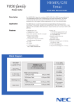
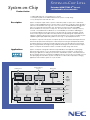
SYSTEM-ON-CHIP LITE +
System-on-Chip
Extended ARM7TDMI-STM-based,
customizable microcontroller
Product Letter
• ARM7TDMI-S-based customizable microcontroller
• Development platform for ARM7TDMI-S-based System-on-Chip design
• Easy development and verification flow
Description
System-on-Chip Lite+ is part of NEC’s System-on-Gate-Array family concept for low- to mid-volume
system-on-chip and ARM-based microcontroller solutions. The System-on-Chip Lite+ single-chip device
is based on standard ASIC technology and consists of two blocks: an ARM7TDMI-S-based subsystem
and a sea-of-gates type gate array ASIC area. These blocks are interconnected via the AMBATM
AHB and APB buses. In System-on-Chip Lite+, the subsystem features a multi-port memory
controller, a 10/100M EthernetTM Media Access Controller (MAC) and an AHB-to-AHB bridge for
accessing the AHB bus from the gate array area. The subsystem also includes an interrupt controller,
a timer, a watchdog timer and a UART. This subsystem block is fully predesigned and preverified as a
supermacro. Using the gate array area connected to this supermacro, the customer can expand system
capabilities significantly by implementing additional custom logic or special peripheral functions.
An important component of the System-on-Chip Lite+ product is the FPGA-based development board
that functionally represents the final System-on-Gate-Array device. Using the development board with
an FPGA and System-on-Chip Lite+ prototype chip (ie, the microcontroller subsystem only), the target
device is pregenerated by the designer using a familiar FPGA design flow. Then in the final short step to
System-on-Chip Lite+ the FPGA RTL-netlist is converted to the ASIC design environment.
Applications
System-on-Chip Lite+ is designed for Ethernet-ready embedded control applications requiring high
data transfer rates and fast access to the external memory. System-on-Chip Lite+ can be used for a
wide range of applications, including factory automation, industrial bus systems, card readers, business
phones, terminals and home communication equipment. Because of its low unit cost, low NRE cost and
short prototyping turnaround times, System-on-Chip Lite+ is an ideal solution especially for emerging
applications where market acceptance is as yet uncertain.
External Memory
JTAG Interface
MII Interface
8/16/32-bit
10/100M
Ethernet
MAC
Debug Port
Boot
ROM
(3 Kbytes)
ARM7TDMI-S TM
Memory Controller
(SDRAM/SRAM)
AHB1
AHB2
AHB3
AHB2APB
Bridge
SRAM
(8 Kbytes)
AHB2AHB
Bridge
AHB4
APB
IRC
Timer
Watchdog
Interrupt
UDL
(User
Defined
Logic)
Master
Slave
Slave
UART
PLL
Features
• ARM® subsystem
- ARM7TDMI-STM core
- 32-bit ARM® and 16-bit Thumb® instruction set
- 32-bit x 8-bit Multiplier
- SRAM: 8 Kbytes
- Mask-ROM: 3 Kbytes
- Operating frequency: up to 60 MHz
- 10/100M EthernetTM MAC
- Multi-port memory controller supporting:
- SDRAM, Flash (standard/page mode), SRAM
and ROM
- Programmable interrupt controller:
32 interrupts, 8 priority levels
- Peripherals: UART, timer, reset, watchdog,
- JTAG interface for debug and boundary scan
• User-defined logic (UDL) area for custom function
integration
- Sea-of-Gates type 0.25 µm drawn gate length Gate Array
ASIC architecture
- Two UDL size options:
- Option A: up to 250K raw gates
- Option B: up to 440K raw gates
- AHB and APB interconnection to the ARM7TDMI-STM
subsystem
• Operating voltage: 2.5 V + 0.25 V
• I/O voltages: 2.5, 3.3 and 5 V compatible
• Temperature range: -40 to +85°C
• Packages:
- 240-pin FPBGA for UDL option A
- 256-pin BGA for UDL option B
Functional Block Description
CPU
The System-on-Chip Lite+ CPU is the popular ARM7TDMI-S, an ARM7 32-bit
RISC processor core with the Thumb extension, on-chip debugging and 32 x 8
multiplier. Thumb offers 32-bit RISC performance at 16-bit system cost through
“compression” of the original ARM instruction set, resulting in high code density
that saves memory space. The Thumb instructions are “decompressed” on the fly
into full 32-bit ARM instructions. It is also possible to select between ARM and
Thumb modes during instruction execution.
Bus System
The ARM7TDMI subsystem includes a fully AMBA compliant bus system
structure. Two main buses – AHB and APB – connect the different macros. The
AHB is a high-speed multi-master bus for connection to high-speed macros like
CPU and memory controller. The APB is the standard bus for peripherals like
UART, timer, etc. Both buses are 32 bits wide. The AHB and the APB and any
additional signals required for interrupts and reset are made available to the UDL.
Memory
The memory subsystem features an internal 8-Kbyte RAM and a small 3-Kbyte
ROM. The ROM contains a bootstrap loader program, selectable via an external pin.
Memory Controller
The System-on-Chip Lite+ multi-port memory controller supports SDRAM (at up
to 100 MHz), static memory-mapped devices including SRAM, ROM and Flash
(standard/page mode). The address range per chip select is 64 Mbytes.
10/100 EthernetTM
Media Access Controller (MAC)
The 10/100M Ethernet MAC is compatible with the IEEE802.3 standard, featuring
an address checker, control and statistics registers. It is connected to the multiport memory controller via the AHB bus to enable high data throughput and to the
system AHB bus for configuration. Interfacing to the outside world is via a Media
Independent Interface (MII).
Interrupt Controller
The interrupt controller supports 32 interrupts: 29 interrupts from the UDL and
3 from the ARM subsystem. All interrupts are priority-controlled, individually or
globally maskable and selectable by triggering the IRQ of the ARM core.
SYSTEM-ON-CHIP LITE +
Extended ARM7TDMI-STM-based,
customizable microcontroller
Peripherals
The subsystem contains a simple UART supporting auto-synchronization and a timer
consisting of a 32-bit down counter with load registers. A configurable prescaler generates
the timer clock frequency. A second timer is used as a watchdog timer, generating a reset
on overflow.
UDL
System-on-Chip Lite+ will be available in two options: with up to 250k raw gates or 440k
raw gates in a sea-of-gates-type gate array area. The UDL area is connected with the
subsystem via the AHB and the APB bus and is available for custom functions. These can
be additional peripheral blocks, third-party intellectual property blocks and hardwired logic
function blocks (eg, for DSP-type functions).The custom logic is implemented in the
System-on-Chip Lite+ chip using NEC’s gate array ASIC design flow. NEC supports the
customer during the implementation phase. NEC also offers FPGA conversion services for
customers who are not familiar with the standard ASIC design flow.
Ordering Information
Devices
Part number
Package
Brand name
µPD66702-Pxx
(up to 250 K raw gates)
240-pin FPBGA
System-on-Chip Lite+
µPD66703-Pxx
(up to 440 K raw gates)
256-pin BGA
System-on-Chip Lite+
Note: Two digits (xx) are reserved for the customer specific suffix number
Documentation
Tools
Doc reference
Topic
Type
A17158EE
System-on-Chip Lite+
User’s Manual
A17364EE
System-on-Chip Lite+
Data Sheet
A16902EE
System-on-Chip Lite+
Brochure
A17207EE
Development Board
Product Letter
A17459EE
Development Board
User’s Manual
A15047EE
Design Flow
Product Letter
A17646EE
Start it! Development Board
User’s Manual
Order number
Description
EB-SOCLITEPLUS-EP1S60V1
Development Board
EB-SOCLITEPLUSSTARTIT-V1
Starter Kit “Start it!”
SYSTEM-ON-CHIP LITE +
Extended ARM7TDMI-STM-based,
customizable microcontroller
NEC Offices
NEC Electronics (Europe) GmbH
Arcadiastr. 10, 40472 Düsseldorf, Germany
Tel. 0211 65030, Fax 0211 6503-1327
- Podbielskistr. 164, 30177 Hannover, Germany
Tel. 0511 33402-0, Fax 0511 33402-34
- Werner-Eckert-Str. 9, 81829 München, Germany
Tel. 089 921003-0, Fax 089 921003-15
- Industriestr. 3, 70565 Stuttgart, Germany
Tel. 0711 99010-0, Fax 0711 99010-19
- Sucursal en España, Juan Esplandiu 15, 28007 Madrid, Spain
Tel. 091 504-2787, Fax 091 504-2860
- Succursale Française, 9, rue Paul Dautier, B.P. 52, 78142 Vélizy-Villacoublay Cédex, France
Tél. 01 306758-00, Fax 01 306758-99
- Filiale Italiana, Via Fabio Filzi, 25A, 20124 Milano, Italy
Tel. 02 66754-1, Fax 02 66754-299
- Branch The Netherlands, Limburglaan 5, Postbus 863, 5600 AW Eindhoven, The Netherlands
Tel. 040 265 4010, Fax 040 244 4580
- Tyskland Filial, Täby Centrum, Entrance S (7th floor), 18322 Täby, Sweden
Tel. 08 638 7200, Fax 08 638 7222
- United Kingdom Branch, Cygnus House, Sunrise Parkway, Linford Wood,
Milton Keynes, MK14 6NP, United Kingdom
Tel. 01908 691133, Fax 01908 670290
Web:
www.eu.necel.com
Offices world-wide:
www.eu.necel.com/global
Distributors in Europe: www.eu.necel.com/distributors
© Published by NEC Electronics (Europe) GmbH, Printed in Germany, November 2005
Document No. A16582EE6V0PL00
ARM7TDMI, ARM7, ARM and Thumb are registered trademarks of ARM Limited. ARM7TDMI-S and AMBA are trademarks of
ARM Limited. Ethernet is a trademark of Xerox Corporation.
With compliments
NEC makes no warranty with respect to this documentation and disclaims any implied warranties of merchantability or fitness for particular
purpose. NEC does not assume any responsibility for circuits shown or claim that they are free from patent infringement. Please be aware that this
is an advanced notice. Thus product specifications are subject to change without notice. To ensure that you have the latest product data, please
contact your local NEC sales office.
©
NEC Electronics (Europe) GmbH