1
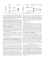
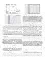
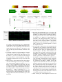
Transmitting TLM transactions over analogue wire models
Stephan Schulz, Jörg Becker, Thomas Uhle, Karsten Einwich
Sören Sonntag
Fraunhofer Institute for Integrated Circuits IIS
Design Automation Division
Zeunerstr. 38, 01069 Dresden, Germany
Lantiq Deutschland GmbH
Design Platforms & Services
Neubiberg, Germany
Abstract—Nowadays digital systems have very high switching
frequencies. Hence analogue effects can have a serious impact
on data transmissions of connected modules in System-on-Chip
(SoC) designs. The implications include attenuation, delay, and
others which have to be considered as important effects. However,
analogue technology models comprise too many details to be
usable at system level as the simulation time would be far to
high compared to traditional Transaction Level Modelling (TLM)
models.
In this paper we illustrate different aspects of using analogue
line models as a transmission method for transactions between
TLM models. This includes the introduction of analogue signal
paths for TLM models and how to avoid the simulation time
penalty of analogue technology models. We show how we can
even use this approach to apply analogue effects to electronic
system level (ESL) performance evaluations by further reducing
the amount of details of the analogue effects.
system. If they are not taken into consideration in the system
during verification, they will not be discovered until hardware
prototypes are examined. That results in a huge cost factor
for the redesign of the whole system to work around these
unwanted analogue effects.
To manage this issue in an early phase of the system design,
an analogue line model is used to transmit TLM transactions.
This model is adjusted by values gathered from a simulation
with a customised analogue technology model of a given
physical interconnect. Transmission errors caused by high
switching frequencies can be prevented in the digital systems
by using error correction or other similar methods with respect
to analogue line models.
I. M OTIVATION
Further motivation is given by the fact that parallel transmissions are rising problems concerning crosstalk and die area in
System-on-Chip designs. Crosstalk and jitter are strengthened
to a great deal because of chip shrinking which makes parallel
lines more vulnerable to these effects. Higher bus frequencies
of currently designed chips are even reinforcing these analogue
effects. Thus, serial transmissions are introduced to be able
to drive higher bus frequencies while rising data throughput,
or at least maintaining it, while saving die area. In computer
systems the most notable example for this is the switch
from parallel (PATA) interfaces to serial (SATA) interfaces
for magnetic and optical storage devices while offering higher
data throughput. The switch from parallel to serial interfaces
is not limited to off-chip interconnects but is also prevalent in
on-chip interconnects.
It is desirable to incorporate analogue effects in higher abstraction levels since the limitations of transmission throughput
can be considered in the design process of the whole system.
Analogue line models have to be simplified as they exhibit
slow simulation speed that prevents the simulation of a large
amount of lines as needed in SoC designs. However, the
high number of analogue details is not necessary for higher
abstraction levels as we will show in this paper.
U
1
sing OSCI TLM -2.0 for system simulation holds some
important benefits. The high level of abstraction makes
it unnecessary to compute the signals of every pin which
results in very high simulation speeds. Even very complex
systems can be designed faster because the communication
between modules is focused on transmitted data itself and
not its transmission method. Thus, the physical layer of
communication is not present in TLM-2.0 [1].
With our developed SystemC-AMS [3, 4, 9] line module, we
have gained a speed-up of 6 · 104 in simulation time compared
to a simulation with an analogue model resulting from layout
extraction while maintaining all analogue effects.
A. Analogue effects in digital systems
A common problem in today’s systems are high switching
frequencies that introduce analogue effects to the transmission
paths of a digital system. These effects lead to transmission
errors on an otherwise digital driven interconnect. Those errors
have to be corrected or prevented in the first place and
should be considered while simulating and verifying a given
This work has been developed in the project RapidMPSoC. RapidMPSoC
(project label 01M3085) is partly funded within the Research Programme ICT
2020 by the German Federal Ministry of Education and Research (BMBF).
The authors are responsible for the content of the paper.
1 TLM (Transaction Level Modelling) is a design method which focuses on
data transmission between two modules without considering the transmission
in a real hardware. The Open SystemC Initiative (OSCI) TLM Working
Group released a user manual [6] for their interpretation of transaction level
modelling, called TLM-2.0. This standard is used interchangeable to the
general term TLM in this paper.
978-3-9810801-6-2/DATE10 © 2010 EDAA
B. Serial transmission
II. A DDING A SIGNAL PATH TO TLM-2.0
SystemC [5] modules are usually connected by discrete event
signals of a specified type. This does not apply for TLM
modules which are connected sockets defined in TLM-2.0
[6]. These sockets will provide interfaces for the actual TLM
transmission. TLM-2.0 defines three classes of interfaces:
Figure 1.
Abstract transmission of a transaction according to TLM-2.0
transport, direct memory, and debug transport. In our case
we only use the transport interface in its non-blocking mode.
Blocking transport can be easily replicated if needed and will
not be covered explicitly. Therefore, on all occasions the nonblocking transport interface is assumed.
The interfaces introduce certain methods which have to be
implemented by TLM initiators and TLM targets. An initiator
in the sense of TLM is a module which transmits or requests
data from a target and is therefore the active component on an
initiator-target connection. Usually, a SystemC module with
TLM sockets also implements its interfaces, though this is
technically not enforced. Addtionally, a SystemC module can
be an initiator to multiple targets as well as a target to multiple
initiators or both at the same time.
Because communication between initiators and targets is
implemented using sockets which provide interfaces, transmitting a transaction is only a method call from one SystemC
object to another with the transaction being only referenced
by a parameter (see Fig. 1).
Consequently, no explicit signal path exists to transmit the
transaction. Because there is no transmission of the actual
transaction data, no delay or modification can be introduced
without changing the initiator or target of a given transaction.
A. Transmitting transactions
A TLM interconnect module was developed for compensating this problem, which is called ‘Debugged Interconnect’. Interconnect modules in the context of TLM are SystemC modules which act as an intermediate pass-through for transactions.
They have the ability to modify and delay a transaction within
the forward and backward path of a transaction transmission
but never create a transaction of their own nor are they a final
target.
Our goal is that a transaction reaches its target after the
amount of time which is needed to transmit its payload over
any given line model. Additionally, all transmission errors
which occur due to physical constraints of the line model
should be visible in the payload but not in the accompanying
transaction flags and data fields. The benefit of such an
interconnect module is, that no changes to the module logic
are required in the original initiator or target modules.
The insertion of an interconnect module and its impact
on transaction transmission can be seen in Figure 2. The
delays which result from sending the transaction payload over
an arbitrary line model are displayed in red. Those delays
Figure 2. Abstract transmission of a transaction according to TLM-2.0 with
an interconnect module inserted
will be determined by the analogue line model during the
simulation. Any transmission error would only be visible in
the payload to the transaction receiver. Flags and data of the
transaction object will stay unmodified as the handling of
transmission errors in these meta-data would complicate the
whole transaction handling and would not add any value to
our simulation efforts.
B. Modifying transactions
Each debugged interconnect module presents an interface
to delay and modify a bypassing transaction payload using
call-back mechanisms. This interface was introduced to keep
the interconnect module generic for other use-cases. Every
module which utilises this interface is called an ‘adaptor’.
These adaptors have to register themselves to the specific
interconnect module whose transactions shall be intercepted.
If no adaptors are registered to a debugged interconnect, it
will not modify or delay the transaction in any way and will
not be noticed by any measurement due to this reason. The
system will behave as shown in Figure 1.
If a transaction reaches an interconnect with at least one
registered adaptor, every adaptor is given the chance to modify
or delay the transaction. Therefore the functionality of driving
an arbitrary line model is contained in an adaptor which
registers to such an interconnect. In Section IV we will
describe how we connect the analogue line model using these
adaptors into a TLM model to simulate physical constraints
of transaction payload transmissions over an analogue line.
There are also several other appliances as co-verification and
logging of transactions which are not the focus of this paper.
III. A NALOGUE LINE MODEL
Models of analogue lines resulting from layout extraction are
extremely detailed. Thus, slow simulation speeds of these
models make them inadequate in system level design.
Our model results from a layout extraction of an extracted
real chip: A simulation of 1 ns of a data transmission with
this model, excluding any Device Under Test (DUT), takes
approximately 20 minutes. Adding a netlist with four DUTs
slows down the simulation speed to 45 minutes for 1 ns of
simulated time. These values were gathered while simulating
the model of the circuit resulting from layout extraction shown
in Figure 3. A commercial SPICE-like simulator was used to
gather these results.
Figure 3.
Selected part with line and buffer
Figure 5.
Figure 4.
Simulation of a model from layout extraction
The solution to use analogue line models in system level
design nonetheless lies in using an adjustable SystemC-AMS
line model. The parameters of this SystemC-AMS model are
extracted from the results of a simulation with the model from
layout extraction.
The key idea behind our SystemC-AMS line model is
to do the time consuming simulations only once and build
lookup tables from the simulation results. These lookup tables
are used afterwards during the system level simulation with
SystemC TLM and SystemC-AMS.
A. Prerequisites
The starting point for our investigations is to consider that
the line model is only used for the transmission of digital data.
Thus, we can use some simplifying assumptions for the system
simulation. It is known that the signals on the lines change
only between the digital states 0 (low) and 1 (high). The
input signals shall be represented by a superposition (linear
combination) of a finite number of delayed step signals, which
maybe include a given rise and fall slope. In that case it is
possible to compute the input and output signals of the circuit
with the model from layout extraction for each change of the
step signals in a preparing step. Furthermore, it is possible
to represent also the output signals as linear combination of
delayed step responses by using the values of the lookup
tables. The size of the lookup tables depends on the step
response granularity and has to be chosen by the user.
B. Getting the model’s parameters
An interconnect of a multi-chip system consists of several
short lines connected by refresh buffers. These are necessary
as otherwise the signal would be too much attenuated at the
Signal response in forward mode simulation
receiver’s end to be recognisable. The first step is to select
a typical part of the interconnect design. Figure 3 depicts
such a typical part containing lines and buffers. This approach
also speeds up simulation and parameter extraction as there
is no need to simulate the complete interconnect repeatedly.
Only the highlighted part is used for the current simulation
and parameter extraction for this reason. As our SystemCAMS line model is cascadable, there is no reason to simulate
interconnects consisting of multiple typical parts.
The complete, unchanged netlist from layout extraction is
still necessary to get the rising time of the output of the
DUT which was measured as 70 ps (see Fig. 4). Now the
selected typical part can be detached as DUT for extracting
parameters of this line model. Input of the DUT is the output
of a voltage source with the given rising time of 70 ps and
a series impedance matching the line impedance of the DUT.
The schematic of the DUT is shown in Figure 3.
The DUT has to be simulated twice, to get rise time,
delay, and signal level in forward and reverse mode. This data
is necessary for the SystemC-AMS line model (see Section
III-A) to simulate accurately (e.g. signal reflexions at the end
of the line). In forward mode simulation the voltage source
with the series impedance is connected to the DUT’s input.
As a real load the input of a second DUT is connected to the
output of the examined DUT. Everything else of the second
DUT stays disconnected as we only need the load behaviour of
it. In reverse mode simulation the voltage source is connected
to the DUT’s output. The output of another DUT is connected
as a real load to the input of the examined DUT. As before all
remaining connectors stay disconnected on the second DUT.
Both circuits are combined in one netlist to create a single
data file with all necessary traces in a single run. These four
DUTs simulated at once consume a simulation time of about
45 minutes for 1 ns simulated time. This highlights that it
is simply impractical to simulate whole systems that way.
Figure 5 clearly shows the delay of the analogue line model
in forward mode but no relevant signal flow was measured in
reverse mode.
C. Using the model’s parameters in SystemC
The simulation data previously simulated with the model
from layout extraction was used to simulate its behaviour with
SystemC-AMS. For this purpose a SystemC-AMS module was
developed which reads the parameter file at simulation start
and adjusts its behaviour accordingly as already described
in [8]. The user of the SystemC-AMS line model has to
determine the simulation time resolution. Thus, the read data
can be interpolated and normalised and then be stored in
lookup tables. The interpolation method (linear or quadratic
splines) can be chosen by the user as well. Furthermore, the
signal delay is also computed from the simulation data of the
model from layout extraction.
D. Simulation cycle of the SystemC-AMS line model
The sequence of input voltages ve1 is examined with regard
to value changes (change from 0→1 or 1→0) at every time
step. After detecting a value change the current voltage value
ve1 (tn ), the corresponding voltage difference ∆ve1 (tn ) =
ve1 (tn )−ve1 (tn−1 ), and the time tn are stored within a record
which is added to a FIFO buffer. The simulation steps can be
triggered by SystemC discrete-event signals.
As already mentioned, the current values of the input and
output signals can be represented by a linear combination of all
signal changes up to the current simulation time, for instance
X
v2tab (t − tn ) ∆ve1 (tn ) ,
v2 (t) =
(1)
tn <t
v2tab
where
denotes the appropriate tabulated step response
matching the sign of ∆ve1 (tn ). With proceeding simulation
time the sum grows. This would clearly impede the simulation
speed. But we assumed furthermore that v2tab (t) remains almost
constant for t ≥ t` (steady state). Then it follows
X v2tab (t − tn ) ∆ve1 (tn )
tn ≤t−t`
X
= v2tab (t` )
∆ve1 (tn )
tn ≤t−t`
=: k1 (t)
and combined with (1)
X
v2 (t) = k1 (t) +
(2)
tab
v2 (t − tn ) ∆ve1 (tn ) .
(3)
t−t` <tn <t
A special procedure avoids the accumulation of rounding errors during transient simulation with long simulation intervals.
This procedure is explained in the following paragraph.
The records in the FIFO buffer are sorted with respect
to their time stamps. A record for which t − tn is greater
than the settling time t` of the appropriate step responses
is removed from the FIFO buffer. Thus, this record does no
longer contribute to the sum in (3). Because of
X
∆ve1 (tn ) = ve1 max tn
(4)
tn ≤t−t`
tn ≤t−t`
we can easily compute the constant k1 , which means that the
voltage value stored in the record is multiplied by v2tab (t` )
and assigned to k1 (see (2)). The constant k1 equals zero at
the beginning of the simulation (initial state of zero) and is
updated correspondingly only if a record is to be removed
from the FIFO buffer. For this reason the FIFO length cannot
be greater than a fixed number which can be computed from
the settling time t` and the clock frequency.
On top of the SystemC-AMS line module a hierarchical
SystemC module has been created which comprises the DUT
in Figure 3. It consists of the line model itself and a module
which detects threshold crossings. The threshold voltage of
the circuit’s buffers has been determined by means of the
simulation of the model of the previous mentioned typical
part of the chip interconnect from layout extraction. But the
threshold voltage in our SystemC-AMS module may also be
assigned by the user. Furthermore, it can be parameterised to
represent an arbitrary number of line sections in series. In this
way, an arbitrary length of the modelled interconnect can be
simulated.
As a result the duration of a given simulation is only a
fraction of the original duration to simulate the model from
layout extraction while maintaining the same analogue effects.
IV. I NTEGRATION OF THE ANALOGUE
LINE MODEL INTO TLM-2.0
For the simulation of an analogue transmission of a transaction’s payload it is not enough to have the debugged
interconnects (see section II-A) and the representation of an
analogue line model as SystemC-AMS model. The challenge is
that both are not connectable in a direct way because SystemCAMS and TLM-2.0 have no specified common interfaces to
communicate with each other.
A. Connecting SystemC-AMS to TLM-2.0
This was solved by developing adaptors which register
themselves to debugged interconnects (see II-B) for reading
and writing to a SystemC-AMS model. The architecture and
implementation of the debugged interconnect are offering the
use of a combined adaptor for reading and writing to the
SystemC-AMS model, but for reasons of clarity and logic
we used two debugged interconnects with a single adaptor
registered to each one. For simulation purposes it makes no
difference if they are combined or separated.
The resulting transaction transmission layout is displayed in
Figure 6: TLM initiator and target are the same modules as in
the original design (see Fig. 1) and are connected with each
other through two debugged interconnect modules (similar to
Fig. 2). The analogue sender is a registered adaptor to the
debugged interconnect on initiator side while the analogue
receiver is a registered adaptor to the target side. Both are
connected to the analogue line model through SystemC-AMSprovided analogue signal ports.
B. Transmitting transaction payload
The original transaction transmission process is split into
several transmissions which are not visible to the initiator or
target:
1) The initiator calls the TLM transportation method of the
first debugged interconnect to transmit the transaction.
This is transparent to the initiator because the correct
binding (and therefore the correct interface) is provided
Figure 6.
Figure 7.
Figure 8.
Coupling of the analogue line model with a TLM-2.0 model
Transmission of a transactions payload through an analogue line model
Waveforms of a transmission start
by a netlist as given in Figure 6. It is not differentiable
for the initiator by means of TLM if the interface it has
called is the one of the original target or the interconnect
module. Therefore, the behaviour of the initiator is the
same as if the target would be directly connected to the
initiator.
2) As already described in Section II-B, the debugged
interconnect notifies any registered adaptor of an incoming transaction. Therefore the write adaptor is given
the chance to process the transaction. The debugged
interconnect waits for an acknowledgement of the adaptor that the transaction has been processed after the
notification.
3) The processing of the transaction in the write adaptor
starts with transmitting the transaction payload immediately via the analogue channel (see signal writeOut1
in Fig. 8) with a configurable clock frequency. In order
for proper synchronisation, a transmission is announced
by a high-low signal sequence immediately followed by
the bit-representation of the transaction payload. Thus,
the payload 100 results in a transmission of 10100 as
shown in Figure 8. If the adaptor finished sending the
transaction payload, an acknowledgement is given to the
debugged interconnect that it has finished to process the
transaction.
4) Given the acknowledgement from its only adaptor, the
debugged interconnect on the initiator side forwards the
transaction. As mentioned before regarding the initiator,
the debugged interconnect is not aware of which module
is connected to its initiator port. The transaction is
forwarded to the debugged interconnect on the target
side as given by the netlist of Figure 6. This debugged
interconnect works completely similar to the previous
debugged interconnect which means to notify the read
adaptor, and wait for the acknowledgement to forward
the original transaction.
5) The read adaptor withholds the acknowledgement until
a transmission was completely received from the analogue line model. Therefore any delay in the analogue
line model will also delay the original transaction. As
shown in Figure 8, the delay of this simulation was
about 500 ps. The read adaptor synchronises itself to the
transmission by waiting for the aforementioned highlow-signal sequence. Anything received afterwards is
treated as payload bits of the transaction’s payload.
The length of a payload transmission in bits is known
to the read adaptor beforehand but could be completely
detectable by using a special bit sequence which is
not generated by encoding an arbitrary payload. By
completion of the transmission, the value of the original
transaction payload is replaced by the received payload
from the analogue line model. Any transmission errors
are therefore present in the later transaction process
but could be detected already in the read adaptor by
comparing the payload received from the analogue line
model with the one received with its notification from
the debugged interconnect. This mechanism can be used
to eliminate permanent transmission errors.
6) After receiving the acknowledgement from the read
adaptor, the transaction is forwarded to the intended
target.
Following these steps, the transmission has been delayed
according to the constraints of the analogue line model and
contains all transmission errors which may have happened.
Source of transmission errors can be e.g. driving the clock
frequency too high or line attenuation which both could
lead to problems in detecting high and low signal values
properly. This detection problem arises when signal values
could not reach their voltage completely because the next bit
pulls down or pulls up the voltage of the current value. In
extreme situations this results in an indistinguishable signal
noise where no message could be received properly.
The whole transmission process measured to simulation
time is displayed in Figure 7. Red simulated time indicates
delays introduced due to the analogue line model. The simulated time of the payload transmission is c · (pb + sb ) + d
where pb is the bit-length of the payload, sb is the bit-length
of any used synchronisation and c is the time for a whole
clock cycle. The variable d is determined by the transport
delay imposed by the wire model which makes the difference
between needed simulated time for the write and read adaptor.
Additionally, a payload transmission reaches the read adaptor
before a transaction notification if the transport delay of the
analogue line model is shorter than the time to write the
payload to the analogue line model.
V. S IMPLIFIED LINE MODELS IN PERFORMANCE
EVALUATION
Apart from TLM simulations our approach can be extended to
Electronic System Level (ESL) performance evaluations where
the level of abstraction is higher than TLM. At performance
abstraction communication timing is important while data is
negligible. Performance simulations have the advantage of
high simulation speed up to one order of magnitude higher
than TLM simulations.
In order to further abstract communication, we have implemented a simple channel that reflects timing by utilising
the size of the message to be transmitted. Analogue effects
have to be abstracted and can be included in the model using
statistics for transmission errors. In case of a transmission error
the message is marked as corrupted by the channel. We define
two different cases: a) recoverable transmission errors and b)
non-recoverable errors. In the former case, the receiver has
to take care about proper message recovery. At performance
abstraction this typically affects timing but has no influence
on the message itself. In the latter case, however, the message
must be deleted by the receiver and a re-transmission must be
set up.
For our performance evaluations we use the SystemQ [7]
framework which provides several class libraries to model the
aforementioned behaviour.
VI. R ELATED WORK
A similar approach was used in [2]. In this paper a loosely
timed TLM model (TLM-LT) was coupled with timed syn-
chronous data flow (TDF) models. These TDF models were
written in SystemC-AMS. In contrast we use the approximately timed TLM models (TLM-AT) which frees us from the
issues with the loosely timed models described in this paper.
Although the TLM-LT models may be faster, we have yet to
hit a design where this would justify the effort to solve the
mentioned problems about ‘twisted time warps’ opposing to
the more easily to implement TLM-AT models.
VII. C ONCLUSIONS AND FUTURE WORK
As shown in this paper, transaction level modelling (TLM)
can be adapted to include analogue transmission effects while
maintaining a high simulation speed. The use of an abstract
analogue line model instead of the analogue line model resulting from layout extraction, yields a speed-up of simulation
time from 20 minutes per 1 ns simulated time (without DUTs)
to approximately 20 ms per 1 ns simulated time (including
DUTs) which is a speedup factor of 6 · 104 . With this
factor in mind, it is possible to design a whole TLM system
with analogue transmissions without having simulation times
beyond any practicability. This speedup can be increased by
abstracting the analogue transmission to fit performance evaluation needs while maintaining its effects on transmissions.
For demonstration purposes the current model uses only unidirectional payloads. Support for bidirectional payloads can be
easily added in the same way the unidirectional model works
by sending the payload over the analogue line model a second
time. Further enhancements for simulating analogue effects on
digital transmissions are planned. The next step is the incorporation of crosstalk. This has been already implemented in the
SystemC-AMS line module but layout data of the current chip
technology is still missing. An interesting issue of crosstalk is
that transactions can be interrupted or injected by unexpected
start/end-of-packet symbols. Additionally synchronisation bits
missed by the analogue reader also need investigations because
probably the whole payload will be missed or read in the
middle of the transmissions.
R EFERENCES
[1] L. Cai and D. Gajski. Transaction level modeling in system level design.
Technical report, University of California, Irvine, March 2003.
[2] M. Damm, C. Grimm, J. Haase, A. Herrholz, and W. Nebel. Connecting
SystemC-AMS Models with OSCI TLM 2.0 Models Using Temporal
Decoupling. In Proceedings of Forum on Design Languages (FDL’08),
2008.
[3] OSCI AMS Working Group. An introduction to modeling embedded
analog/mixed-signal systems using systemc ams extensions. 7th Symposium on Electronic System-Level Design with SystemC, June 2008.
[4] OSCI AMS Working Group. OSCI SystemC Analog Mixed-Signal
Extensions, draft 1 edition, December 2008.
[5] OSCI Language Working Group. IEEE Std 1666 - 2005 Standard SystemC
Language Reference Manual, March 2006.
[6] OSCI TLM Working Group. OSCI TLM-2.0 User Manual, June 2008.
[7] S. Sonntag, M. Gries, and C. Sauer. SystemQ: Bridging the gap between
queuing-based performance evaluation and SystemC. In Proceedings of
Design Automation for Embedded Systems, pages 91 – 117, 2007.
[8] T. Uhle, K. Einwich, and J. Haase. Efficient transient simulation of
lossy coupled interconnects in digital communication applications. In
Proceedings of Forum on Design Languages (FDL’07), 2007.
[9] A. Vachoux, C. Grimm, and K. Einwich. SystemC-AMS Requirements,
Design Objectives and Rationale. In Proceedings of Design Automation
and Test in Europe (DATE’03), pages 388 – 393, 2003.