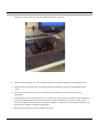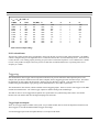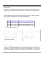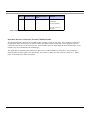
1
eInstrument PC User's Manual
eInstrument PC User's Manual
The eInstrument PC User's Manual was prepared by the technical staff
of Innovative Integration on November 17, 2011.
For further assistance contact:
Innovative Integration
2390-A Ward Ave
Simi Valley, California 93065
PH:
FAX:
(805) 578-4260
(805) 578-4225
email: [email protected]
Website: www.innovative-dsp.com
This document is copyright 2011 by Innovative Integration. All rights
are reserved.
VSS \ Distributions \ eInstrument PC \ Documentation \ Manual \
eInstrument PCMaster.odm
#XXXXXX
Revision
Release Notes
Date
Rev 1.0
Initial release.
10/09/08
Rev 1.1
Corrected table showing mezzanine connections to XMC
modules.
11/21/08
Rev 1.2
Updated clock diagram to add FPGA clock.
01/06/09
Rev 1.3
Added SBC COMEX Rev C motherboard diagrams.
Corrected pinout of J16/J26 for DIOx.
04/16/09
Rev 1.4
Corrected mezzanine mechanical drawing. Added
specifications for 80200-4 DC/DC supply. Update power
consumption table.
11/10/09
Rev 1.5
Fixed connector reference on RevC+ mezzanine drawing.
12/13/09
Table of Contents
eInstrument PC User's Manual................................................................................................................2
Introduction..............................................................................................................................................10
Real Time Solutions!.............................................................................................................................................................10
Vocabulary.............................................................................................................................................................................10
What is Malibu? ........................................................................................................................................................11
What is C++ Builder?.................................................................................................................................................12
What is Microsoft MSVC?.........................................................................................................................................13
What kinds of applications are possible with Innovative Integration hardware?.......................................................14
Why do I need to use Malibu with my Baseboard?....................................................................................................14
Finding detailed information on Malibu.....................................................................................................................14
Online Help......................................................................................................................................................................14
Innovative Integration Technical Support........................................................................................................................15
Innovative Integration Web Site......................................................................................................................................15
Typographic Conventions......................................................................................................................................................15
Using the eInstrument PC.......................................................................................................................16
Getting Started.......................................................................................................................................................................16
Setting Up the eInstrument PC..............................................................................................................................................16
For Innovative X5 family of modules:.............................................................................................................................18
For Innovative X3 family of modules:.............................................................................................................................20
Installing a disk drive:......................................................................................................................................................22
TroubleShooting....................................................................................................................................................................24
The eInstrument PC will not boot up...............................................................................................................................24
The eInstrument starts to boot then the screen goes blank when Windows is booting....................................................25
The XMC is not recognized.............................................................................................................................................25
The Linux HDD is not recognized...................................................................................................................................25
Insufficient room of Flash boot drive for development tools..........................................................................................25
Windows Installation...............................................................................................................................27
Host Hardware Requirements................................................................................................................................................27
Software Installation..............................................................................................................................................................27
Starting the Installation ...................................................................................................................................................28
The Installer Program.......................................................................................................................................................29
Tools Registration..................................................................................................................................................................31
Bus Master Memory Reservation Applet...................................................................................................................31
Hardware Installation.............................................................................................................................................................32
After Power-up......................................................................................................................................................................33
Installation on a Deployed System........................................................................................................................................33
Running MalibuRed.........................................................................................................................................................33
Installation on Linux...............................................................................................................................35
Package File Names...................................................................................................................................................35
Prerequisites for Installation..................................................................................................................................................35
The Redistribution Package Group - MalibuRed.............................................................................................................35
Malibu..............................................................................................................................................................................36
Other Software.................................................................................................................................................................36
3
Baseboard Package Installation Procedure............................................................................................................................36
Board Packages................................................................................................................................................................37
Unpacking the Package....................................................................................................................................................37
Creating Symbolic Links............................................................................................................................................37
Completing the Board Install...........................................................................................................................................38
Linux Directory Structure......................................................................................................................................................38
Applets........................................................................................................................................................................38
Documentation...........................................................................................................................................................38
Examples....................................................................................................................................................................38
Hardware....................................................................................................................................................................38
Writing Custom Applications.................................................................................................................39
SBC-ComEx Example Software............................................................................................................................................39
Tools Required.................................................................................................................................................................39
Program Design................................................................................................................................................................40
The Host Application ............................................................................................................................................................40
User Interface...................................................................................................................................................................40
Configure Tab.............................................................................................................................................................40
Clock Tab...................................................................................................................................................................41
Digital I/O Tab...........................................................................................................................................................42
Gps Tab......................................................................................................................................................................43
Trigger Tab.................................................................................................................................................................44
EEProm Tab...............................................................................................................................................................45
Debug Tab..................................................................................................................................................................45
Host Side Program Organization................................................................................................................................45
ApplicationIo....................................................................................................................................................................46
Initialization................................................................................................................................................................46
Using the Programmable Timebase............................................................................................................................48
Using Programmable Bit I/O......................................................................................................................................50
Polling Thread............................................................................................................................................................50
GPS Support ..............................................................................................................................................................51
Developing Host Applications.................................................................................................................15
Borland Turbo C++................................................................................................................................................................15
Microsoft Visual Studio 2005................................................................................................................................................17
Applets......................................................................................................................................................19
Common Applets...................................................................................................................................................................19
Registration Utility (NewUser.exe).................................................................................................................................19
Reserve Memory Applet (ReserveMemDsp.exe)...........................................................................................................20
...............................................................................................................................................................................................20
Data Analysis Applets...........................................................................................................................................................20
Binary File Viewer Utility (BinView.exe).......................................................................................................................20
eInstrument PC Hardware......................................................................................................................21
Introduction............................................................................................................................................................................21
COM Express CPU Site.........................................................................................................................................................23
COM Express Site Compatibility.....................................................................................................................................25
Considerations when Selecting Other COM Express Modules ......................................................................................26
XMC IO Module Sites...........................................................................................................................................................26
4
XMC Module Site Connectivity......................................................................................................................................27
Intermodule Connectivity.................................................................................................................................................29
Front Panel LED from XMC............................................................................................................................................29
XMC Site Identification...................................................................................................................................................30
Ethernet Port..........................................................................................................................................................................30
USB Ports..............................................................................................................................................................................30
SATA and Hard Disk Options...............................................................................................................................................31
FLASH Drive.........................................................................................................................................................................32
Watchdog Timer....................................................................................................................................................................32
Battery and Monitor...............................................................................................................................................................32
Reset.......................................................................................................................................................................................33
Sample Clocks and Triggering Controls................................................................................................................................33
Updates to Rev D........................................................................................................................................................33
Sample Clocking Modes..................................................................................................................................................35
External Clock and Reference Input................................................................................................................................35
Sample Clock Outputs......................................................................................................................................................36
Internal Sample Generation Using PLL...........................................................................................................................36
PLL Output Range and Resolution Limitations.........................................................................................................36
Programming the PLL......................................................................................................................................................37
PLL Lock and Status........................................................................................................................................................39
Triggering..............................................................................................................................................................................39
Trigger Input and Outputs................................................................................................................................................39
Trigger Modes..................................................................................................................................................................41
Trigger Source..................................................................................................................................................................42
Framed Trigger Mode......................................................................................................................................................43
Decimation.......................................................................................................................................................................43
GPS Triggering (Optional Feature)..................................................................................................................................43
Temperature Monitoring and Thermal Design......................................................................................................................44
System Thermal Design...................................................................................................................................................44
Temperature Sensor and Over Temperature Protection..................................................................................................44
Reading the Motherboard Temperature...........................................................................................................................45
Temperature Monitoring .................................................................................................................................................46
XMC Cooling...................................................................................................................................................................46
GPS Receiver Option.............................................................................................................................................................47
GPS Module.....................................................................................................................................................................48
GPS Antenna....................................................................................................................................................................48
GPS Interface ..................................................................................................................................................................48
Cabled PCI Express Expansion Port......................................................................................................................................50
PCI Express Cables..........................................................................................................................................................50
Electrical Isolation and Hot Plug.....................................................................................................................................51
Tuning for PCI Express Cable Lengths and Signal Quality............................................................................................51
EEPROM ..............................................................................................................................................................................52
IO Expansion Mezzanine.......................................................................................................................................................52
Mezzanine IO Connections..............................................................................................................................................52
Mezzanine Interface to Baseboard FPGA........................................................................................................................53
Mezzanine Interface to Innovative X3 and X5 Module Families....................................................................................56
Mezzanine Mechanicals...................................................................................................................................................59
Powering the eInstrument .....................................................................................................................................................59
PC Power Supply.............................................................................................................................................................59
12V DC-DC Supply (80200-1)..................................................................................................................................59
12V DC-DC Supply (80200-4)..................................................................................................................................61
5
External Power Supply.....................................................................................................................................................61
Power Controls.................................................................................................................................................................62
Power Consumption.........................................................................................................................................................62
Environmental Limits ...........................................................................................................................................................63
Connectors.............................................................................................................................................................................64
J28, J29, J30, J31 - SMA Connectors .............................................................................................................................64
J15, J25 - XMC PCI Express Connectors........................................................................................................................65
J16, J26 – XMC Secondary Connectors..........................................................................................................................68
JP1 - Xilinx JTAG Connector..........................................................................................................................................72
JN1 - Rear Mezzanine Connector....................................................................................................................................73
JN2 - Rear Mezzanine Connector (Revision A only)......................................................................................................75
JN2 - Rear Mezzanine Connector (Revision B only).......................................................................................................77
JN2 – IO Mezzanine Connector (Revision C+)...............................................................................................................79
JN3– IO Mezzanine Connector (Revision C+)................................................................................................................81
JP10, JP12, JP15 - USB Headers.....................................................................................................................................83
P2 – Cabled PCI Express Connector................................................................................................................................84
COM Express CPU Site – P1...........................................................................................................................................85
VGA Connector – J27......................................................................................................................................................86
U34, U35, U38, U39 – SATA Ports.................................................................................................................................87
U12 - Ethernet Connector................................................................................................................................................88
JP11- FLASH Drive USB Header....................................................................................................................................89
P5 – ATX Power Connector............................................................................................................................................90
JP17 – GPS Module Connector........................................................................................................................................91
P3 -Rear Panel USB Ports................................................................................................................................................92
Rear Panel Power Jack.....................................................................................................................................................93
Mechanicals...........................................................................................................................................................................94
6
List of Tables
Table 1. eInstrument PC Kit Contents...................................................................................................................................16
Table 2. Development Tools for the SBC-ComEx Example.................................................................................................39
Table 3. eInstrument PC COM Express Site Features...........................................................................................................25
Table 4. COM Express Site Specifications............................................................................................................................26
Table 5. Qualified COM Express Modules...........................................................................................................................26
Table 6. XMC Site Specifications.........................................................................................................................................27
Table 1. XMC Data Connectivity Details..............................................................................................................................28
Table 2. XMC-to-XMC Communications Lanes..................................................................................................................29
Table 3. XMC LEDs..............................................................................................................................................................30
Table 4. XMC Geographic Addresses...................................................................................................................................30
Table 5. Ethernet LED Functions..........................................................................................................................................30
Table 6. USB Port Connectors and Assignments..................................................................................................................31
Table 7. SATA Port Assignments..........................................................................................................................................31
Table 8. Approved Hard Disk Drives....................................................................................................................................32
Table 9. Lithium Battery Type..............................................................................................................................................33
Table 1. Sample Clock Modes...............................................................................................................................................35
Table 2. External Clock/Reference Specifications................................................................................................................35
Table 3. Sample Clock Outputs.............................................................................................................................................36
Table 4. Front Panel Sample Clock Output Specifications...................................................................................................36
Table 5. Allowable Sample Clock Output Ranges using 100-140 MHz VCO......................................................................37
Table 6. Allowable Sample Clock Output Ranges using Programmable VCXO with 10-820 MHz Range.........................37
Table 7. Selecting values for PLL Divisors ..........................................................................................................................38
Table 8. PLL Example Settings.............................................................................................................................................39
Table 1. Trigger Connectors..................................................................................................................................................40
Table 2. Input Trigger Specifications (Front Panel, J31)......................................................................................................41
Table 3. Output Trigger Specifications..................................................................................................................................41
Table 1. Triggering Control (PCI BAR + 0x6A000).............................................................................................................42
Table 2. Software Triggering Control (PCI BAR + 0x5D000)............................................................................................43
Table 3. Decimation Control (PCI BAR + 0x6F000)............................................................................................................43
Table 4. GPS Triggering Control (0x70000).........................................................................................................................44
Table 5. Motherboard Temperature Failure and Warning Levels.........................................................................................44
Table 6. Motherboard Temperature Register (PCI BAR + 0x52000 R)...............................................................................45
Table 7. Motherboard Temperature Failure and Warning Levels.........................................................................................46
Table 8. Motherboard Temperature Warning (PCI BAR + 0x53000) and Failure Registers (PCI BAR + 0x54000)..........46
Table 9. Fan Control Jumper.................................................................................................................................................46
Table 10. Heat Sinks for XMC Modules...............................................................................................................................47
Table 1. GPS Performance.....................................................................................................................................................48
Table 2. GPS Serial Port (PCI BAR + 0x68000)...................................................................................................................49
Table 3. GPS UART Configuration /Status (PCI BAR + 0x6E000).....................................................................................49
Table 4. GPS UART Status and Control (PCI BAR + 0x69000)..........................................................................................49
Table 5. PCI Interrupt Register (PCI BAR + 0x64000, read)................................................................................................49
Table 6. PCI Interrupt Mask Register (0x51000, write)........................................................................................................50
Table 7. Approved PCI Express cable list for eInstrument PC.............................................................................................51
Table 8. Settings for PCI Express Transceiver Switches.......................................................................................................51
Table 9. IO Mezzanine Connector Functions........................................................................................................................53
Table 1. IO Mezzanine Connections to FPGA......................................................................................................................55
Table 2. DIO 31..0 Register (PCI BAR + 0x6B000).............................................................................................................55
7
Table 3. DIO 47..32 Register (PCI BAR + 0x6C000)...........................................................................................................55
Table 4. DIO Enables Register (PCI BAR + 0x6D000)........................................................................................................56
Table 5. IO Mezzanine Connections to XMC Sites (Rev C and later)..................................................................................57
Table 1. eInstrument PC Power Supply 80200-1 Characteristics..........................................................................................60
Table 1. eInstrument PC Power Supply 80200-4 Characteristics..........................................................................................61
Table 2. External Power Supply Specifications.....................................................................................................................62
Table 3. Power Mode Control Jumper JP20..........................................................................................................................62
Table 4. eInstrument PC Power Consumption.......................................................................................................................63
Table 5. eInstrument PC Environmental Limits....................................................................................................................63
Table 1. eInstrument PC XMC Connector P15 Pinout..........................................................................................................66
Table 2. J15/J25 Signal Descriptions.....................................................................................................................................67
Table 1. eInstrument PC XMC Secondary Connector P16/P26 Pinout (rev A only)............................................................69
Table 2. J16/J26 Signal Descriptions (rev A only)................................................................................................................69
Table 3. eInstrument PC XMC Secondary Connector P16/P26 Pinout (rev B only)............................................................70
Table 4. J16/J26 Signal Descriptions (rev B only)................................................................................................................70
Table 5. eInstrument PC XMC Secondary Connector P16/P26 Pinout (rev C+)..................................................................71
Table 6. J16/J26 Signal Descriptions (rev C+)......................................................................................................................71
8
List of Figures
Figure 1. Vista Verification Dialog.......................................................................................................................................28
Figure 2. Innovative Install Program....................................................................................................................................29
Figure 3. Progress is shown for each section.........................................................................................................................30
Figure 4. ToolSet registration form.......................................................................................................................................31
Figure 5. BusMaster configuration........................................................................................................................................32
Figure 6. Installation complete..............................................................................................................................................32
Figure 7. eInstrument PC.......................................................................................................................................................22
Figure 8. eInstrument PC Block Diagram.............................................................................................................................23
Figure 1. XMC Data Connectivity ........................................................................................................................................28
Figure 2. eInstrument PC Sample Clock Diagram (Rev A-C)..............................................................................................34
Figure 3. eInstrument PC Sample Clock Diagram (Rev D)..................................................................................................34
Figure 1. Trigger Connections...............................................................................................................................................40
Figure 1. Sample Trigger Timing..........................................................................................................................................42
Figure 1. X3 heat bars (61121)..............................................................................................................................................47
Figure 2. X5 heat bars (61122)..............................................................................................................................................47
Figure 1. IO Expansion Mezzanine Connections..................................................................................................................53
Figure 2. IO Mezzanine Mechanicals....................................................................................................................................59
Figure 1. Connectors J28-J30 Functions................................................................................................................................64
Figure 2. J15/J25 XMC Connector Pin Arrangement............................................................................................................65
Figure 1. J16/J26 XMC Connector Pin Arrangement............................................................................................................68
Figure 2. JP1 FPGA JTAG Connector Pinouts......................................................................................................................72
Figure 3. JP1 FPGA JTAG Connector Pin Orientation.........................................................................................................72
Figure 4. JN1 Mezzanine Connector Pinout..........................................................................................................................74
Figure 5. JP10, JP12, JP15 USB Header Pinouts..................................................................................................................83
Figure 6. P2 Cabled PCI Express Connector Pinout.............................................................................................................84
See the COM Express Specification for a detailed pinout of this connector.........................................................................85
Figure 7. U34, U35, U38, U39 SATA Connectors Pinout....................................................................................................87
Figure 8. U12 Ethernet Connector Pinout.............................................................................................................................88
Figure 9. JP11 FLASH Drive USB Pinout............................................................................................................................89
Figure 10. P5 ATX Power Connector....................................................................................................................................90
Figure 11. JP17 GPS Connector Pinouts...............................................................................................................................91
Figure 12. P3 Rear Panel USB Ports Pinout..........................................................................................................................92
Figure 13. Rear Panel Power Jack.........................................................................................................................................93
Figure 14. eInstrument PC Motherboard Mechanicals (Top View) Rev B...........................................................................94
Figure 15. eInstrument PC Motherboard Mechanicals (Bottom View) Rev B.....................................................................95
Figure 16. eInstrument PC Motherboard Mechanicals (Top View) Rev C...........................................................................96
Figure 17. eInstrument PC Motherboard Mechanicals (Bottom View) Rev C.....................................................................97
Figure 18. eInstrument PC Front Panel.................................................................................................................................98
Figure 19. eInstrument PC Rear Panel...................................................................................................................................98
Figure 20. eInstrument PC Front View Overall Dimensions.................................................................................................99
Figure 21. eInstrument PC Side View Overall Dimensions..................................................................................................99
Figure 22. eInstrument PC Bottom View Overall Dimensions...........................................................................................100
9
Introduction
Real Time Solutions!
Thank you for choosing Innovative Integration, we appreciate your business! Since 1988, Innovative Integration has grown
to become one of the world's leading suppliers of DSP and data acquisition solutions. Innovative offers a product portfolio
unrivaled in its depth and its range of performance and I/O capabilities .
Whether you are seeking a simple DSP development platform or a complex, multiprocessor, multichannel data acquisition
system, Innovative Integration has the solution. To enhance your productivity, our hardware products are supported by
comprehensive software libraries and device drivers providing optimal performance and maximum portability.
Innovative Integration's products employ the latest digital signal processor technology thereby providing you the competitive
edge so critical in today's global markets. Using our powerful data acquisition and DSP products allows you to incorporate
leading-edge technology into your system without the risk normally associated with advanced product development. Your
efforts are channeled into the area you know best ... your application.
Vocabulary
10
What is Malibu?
Malibu is the Innovative Integration-authored component suite, which combines with the Borland BCB or Microsoft MSVC
Integrated Development Environments (IDEs) to support programming of Innovative hardware products. Malibu supports
both high-speed data streaming plus asynchronous mailbox communications between the DSP and the Host PC, plus a wealth
of Host functions to visualize and post-process data received from or to be sent to the target DSP.
11
What is C++ Builder?
C++ Builder is a general-purpose code-authoring environment suitable for development of Windows applications of any type.
Armada extends the Builder IDE through the addition of functional blocks (VCL components) specifically tailored to
perform real-time data streaming functions.
12
What is Microsoft MSVC?
MSVC is a general-purpose code-authoring environment suitable for development of Windows applications of any type.
Armada extends the MSVC IDE through the addition of dynamically created MSVC-compatible C++ classes specifically
tailored to perform real-time data streaming functions.
13
What kinds of applications are possible with Innovative Integration hardware?
Data acquisition, data logging, stimulus-response and signal processing jobs are easily solved with Innovative Integration
baseboards using the Malibu software. There are a wide selection of peripheral devices available in the Matador DSP
product family, for all types of signals from DC to RF frequency applications, video or audio processing. Additionally,
multiple Innovative Integration baseboards can be used for a large channel or mixed requirement systems and data
acquisition cards from Innovative can be integrated with Innovative's other DSP or data acquisition baseboards for highperformance signal processing.
Why do I need to use Malibu with my Baseboard?
One of the biggest issues in using the personal computer for data collection, control, and communications applications is the
relatively poor real-time performance associated with the system. Despite the high computational power of the PC, it cannot
reliably respond to real-time events at rates much faster than a few hundred hertz. The PC is really best at processing data,
not collecting it. In fact, most modern operating systems like Windows are simply not focused on real-time performance, but
rather on ease of use and convenience. Word processing and spreadsheets are simply not high-performance real-time tasks.
The solution to this problem is to provide specialized hardware assistance responsible solely for real- time tasks. Much the
same as a dedicated video subsystem is required for adequate display performance, dedicated hardware for real-time data
collection and signal processing is needed. This is precisely the focus of our baseboards – a high performance, state-of-theart, dedicated digital signal processor coupled with real-time data I/O capable of flowing data via a 64-bit PCI bus interface.
The hardware is really only half the story. The other half is the Malibu software tool set which uses state of the art software
techniques to bring our baseboards to life in the Windows environment. These software tools allow you to create applications
for your baseboard that encompass the whole job - from high speed data acquisition, to the user interface.
Finding detailed information on Malibu
Information on Malibu is available in a variety of forms:
•
Data Sheet (http://www.innovative-dsp.com/products/malibu.htm)
•
On-line Help
•
Innovative Integration Technical Support
•
Innovative Integration Web Site (www.innovative-dsp.com)
Online Help
The online help system for Malibu is fully integrated into the excellent OpenHelp system provided with Builder. Help for
Malibu is provided in a single file, Malibu.hlp which is installed beneath the main Builder C++ directory tree during the
default installation. It provides detailed information about the components contained in Malibu - their Properties, Methods,
Events, and usage examples. An equivalent version of this help file in HTML help format is also provided: Malibu.chm, for
use within the MSVC context.
14
Innovative Integration Technical Support
Innovative includes a variety of technical support facilities as part of the Malibu toolset. Telephone hotline supported is
available via
Hotline (805) 578-4260 8:00AM-5:00 PM PST.
Alternately, you may e-mail your technical questions at any time to:
[email protected].
Innovative Integration Web Site
Additional information on Innovative Integration hardware and the Malibu Toolset is available via the Innovative Integration
website at www.innovative-dsp.com
Typographic Conventions
This manual uses the typefaces described below to indicate special text.
Typeface
Source Listing
Boldface
Emphasis
Cpp Variable
Cpp Symbol
KEYCAPS
Menu Command
Meaning
Text in this style represents text as it appears onscreen or in code. It
also represents anything you must type.
Text in this style is used to strongly emphasize certain words.
Text in this style is used to emphasize certain words, such as new
terms.
Text in this style represents C++ variables
Text in this style represents C++ identifiers, such as class, function,
or type names.
Text in this style indicates a key on your keyboard. For example,
“Press ESC to exit a menu”.
Text in this style represents menu commands. For example “Click
View | Tools | Customize”
15
Using the eInstrument PC
Getting Started
As delivered, the eInstrument PC has its operating system installed and all options such as FLASH drive and GPS are
installed. Included with the unit are the following:
eInstrument PC
Enclosure with SBC-ComEx motherboard, 125W power PC power supply, COM
Express CPU module, active heat sink for COM Express Module, 4 GB RAM, 4 GB
FLASH drive
Laptop Power Supply
Output is 12VDC, 8.5A (110 W). Input is 100-240VAC, 50-60 Hz.
Power Cord
Modular power cord with US, UK or EU type wall plug. IEC-320 C6 plug for laptop
supply.
Software and Documentation
DVD (also available for download on web)
Microsoft Windows Registration Certificate (Windows only)
Options installed in
eInstrument PC
(90197) GPS Receiver includes external GPS antenna
(80212-0) One Hard Disk Drive, 2.5 in, 200 GB, 7400 RPM
(80212-1) Two Hard Disk Drives, 2.5 in, 200 GB, 7400 RPM
COM Express Modules
(1 of these will be installed)
(90200-0) Radisys CE945GM2A-423-0 Single core Celeron CPU, 1.06 GHz
(90200-1) Radisys CE945GM2A-T25-0 Dual core Core2Duo CPU, 2 GHz
Table 1. eInstrument PC Kit Contents
There are no keyboard, mouse, monitor or other cables included in the unit. The mouse and keyboard are USB type.
Monitor is VGA type.
Setting Up the eInstrument PC
It is a good idea to boot up the eInstrument PC, register the software, then install any software and XMC modules in the
system.
1.
Attach keyboard, mouse and monitor to the rear of the unit.
2.
Attach Ethernet with web access if possible.
16
3.
Attach power supply to the rear of the unit and then plug into the wall power.
4.
The unit will begin booting. You will see a Radisys splash screen and then operating system will begin to boot.
5.
Windows users should register their software using the Microsoft Windows registration card included with the
system.
6.
Once the system is booted, you may want to configure network and other system settings to match your
requirements.
7.
Install software for IO cards and system devices. For Innovative software, follow the instructions in the Windows or
Linux tools installation chapters provided in this manual. For these installations, you must have either network
access to a DVD drive, a local DVD drive attached to a USB port, or internet access. The software installations will
prompt you for shutdown to complete the installation.
8.
Reboot the system and hit F2 to enter the BIOS setup screen.
17
9.
Navigate the BIOS menus to the advanced configurations. Turn on the “ENABLE BUSMASTERING” option and
the “EHNACED PCI EXPRESS COMPATIBILITY OPTIONS”. Set the boot drive ordering to either USB for the
FLASH drive, or SATA drive 0 for the HDD. Disable the optional LVDS display.
10. Save the BIOS to FLASH and then exit the BIOS setup.
You are now ready to install any XMC modules into the eInstrument PC.
For Innovative X5 family of modules:
1.
Shut down the eInstrument PC and DISCONNECT POWER COMPLETELY.
2.
At a static controlled workstation, remove the top cover of the unit. There are 3 screws on each side of the unit to
remove.
3.
Remove the PCB retainer bars on each side of the PCB.
18
4.
Install the XMC on the top of the motherboard in site 0 or site 1 by inserting its end bracket through the front panel
and pressing the XMC down on the card. Be sure to carefully align the XMC module to the connectors. The card
should seat firmly into the connectors.
5.
Remove the two end bracket screws. Now the motherboard can pivot up for access to the bottom side.
19
6.
Install the screws into the heat sink through the bottom side of the motherboard. These are metric M2x5 screws.
7.
Put the motherboard back down into the chassis, and reattach the PCB retention bars on each side. Do not fully
tighten screws yet.
8.
Align the rear panel and install the rear panel screws.
9.
Tighten all screws on the PCB retention bars.
10. Replace the cover and install the screws on each side.
For Innovative X3 family of modules:
1.
Shut down the eInstrument PC and DISCONNECT POWER COMPLETELY.
2.
At a static controlled workstation, remove the top cover of the unit. There are 3 screws on each side of the unit to
remove.
20
3.
Remove the PCB retainer bars on each side of the PCB.
4.
Remove the two end bracket screws. Now the motherboard can pivot up for access to the bottom side.
5.
Install the X3 hear conduction bar on the top the the motherboard, approximately across the center of the module.
There are 5 screws (M2x5) to insert from the bottom side that screw into the bar.
21
6.
Install the XMC on the top of the motherboard in site 0 or site 1 by inserting its end bracket through the front panel
and pressing the XMC down on the card. Be sure to carefully align the XMC module to the connectors. The card
should seat firmly into the connectors.
7.
Add the heat bar screws through the top of the module. These are metric M2x5 screws.
8.
Put the motherboard back down into the chassis, and reattach the PCB retention bars on each side. Do not fully
tighten screws yet.
9.
Align the rear panel and install the rear panel screws.
10. Tighten all screws on the PCB retention bars.
11. Replace the cover and install the screws on each side.
Installing a disk drive:
1.
Shut down the eInstrument PC and DISCONNECT POWER COMPLETELY.
2.
At a static controlled workstation, remove the top cover of the unit. There are 3 screws on each side of the unit to
remove.
22
3.
Remove the PCB retainer bars on each side of the PCB.
4.
Remove the two end bracket screws. The card can now pivot up for access to the drive tray.
5.
Remove the disk drive tray from the bottom of the chassis.
6.
23
7.
Install HDD on the disk tray and reinstall the tray into the chassis.
8.
Plug in power cable and SATA cable to HDD. SATA cable should go to the motherboard SATA connector.
9.
Bundle the SATA and power cables and attach to chassis to prevent cables from getting into the fans.
10. Put the motherboard back down into the chassis, and reattach the PCB retention bars on each side. Do not fully
tighten screws yet.
11. Align the rear panel and install the rear panel screws.
12. Tighten all screws on the PCB retention bars.
13. Replace the cover and install the screws on each side.
TroubleShooting
The eInstrument PC will not boot up.
Check cables and power. During shipping, the COM Express module may have come loose. Inspect the module seating but
do not remove the module unless some problem is visible. The screws holding it have Loctite applied to the threads and may
be difficult to remove.
Some XMC modules have an ID ROM on the IPMI bus. If this is blank or not recognized, the Radisys modules will not
allow the system to boot.
24
The eInstrument starts to boot then the screen goes blank when Windows is booting.
In the BIOS, be sure to disable the optional LVDS screen. Also check the video settings so that VGA is enabled. If the
display still fails to receive a signal, perform the following keystroke combination
Control+Alt+F1
If pressing Control+Alt+F1 fails to revive your display, take the following steps . . .
Make sure a VGA display is connected to your eInstrument-PC
Reboot your eInstrument-PC
Tap F8 repeatedly until the Windows "Boot Options" screen is displayed
Using the arrow keys on your keyboard, select "Enable VGA Mode"
Press Enter
Once Windows boots up, download and run video driver installer (winxp_14324.exe)
Follow the Wizard to complete the installation and reboot
Once Windows is fully booted after this install, your display should be functioning properly.
If the display fails to receive a signal, perform the following keystroke combination
Control+Alt+F1
The XMC is not recognized.
The XMC is not working, installed improperly or has a compatibility issue. On Innovative X3 and X5 modules, the link up
LED indicates whether the PCI Express lane connected. If this LED is off, there is a serious problem. If it is on, then check
the control panel and see if the XMC driver installed properly.
The Linux HDD is not recognized.
Linux has a configuration for each HDD that must be modified. If you change the HDD type, this system file must be
modified. Contact technical support for assistance.
Insufficient room of Flash boot drive for development tools.
The flash boot drive is intended for delivery and execution of a final, debugged executable. It is not large enough to support
all possible development environments. So, my recommendation is to install all development tools onto other hard disk
drives in the system. If the particular tools involved do not support that, then you may be forced to disable the flash drive
using the BIOS setup, or reassign the flash drive as a non-boot drive during the development cycle. You could then install
any OS on a hard disk and use that in conjunction with the eInstrument throughout the development process. Finally, with all
debugging complete, you could reverse the process, install the final executable on the flash and boot/run from flash.
25
26
Windows Installation
This chapter describes the software and hardware installation procedure for the Windows platform (WindowsXP, Vista, and
Windows 7).
Do NOT install the hardware card into your system at this time. This will follow the software
installation.
Host Hardware Requirements
The software development tools require an IBM or 100% compatible Pentium IV - class or higher machine for proper
operation. An Intel-brand processor CPU is strongly recommended, since AMD and other “clone” processors are not
guaranteed to be compatible with the Intel MMX and SIMD instruction-set extensions which the Armada and Malibu Host
libraries utilize extensively to improve processing performance within a number of its components. The host system must
have at least 1 GB of memory (2 GB recommended), 1 GB available hard disk space, and a DVD-ROM drive. Most
versions of Windows released after Win2000 including XP, Vista, or Windows 7 (referred to herein simply as Windows) or
later is required to run the developer’s package software, and are the target operating systems for which host software
development is supported.
Software Installation
The development package installation program will guide you through the installation process.
Note: Before installing the host development libraries (VCL components or MFC classes), you must
have Microsoft MSVC Studio (version 9 or later), CodeGear RAD Studio 2007/2009, Embarcadero Rad
Studio 2010 or QtCreator installed on your system, depending on which of these IDEs you plan to use
for Host development. If you are planning on using these environments, it is imperative that they are
tested and known-operational before proceeding with the library installation. If these items are not
installed prior to running the Innovative Integration install, the installation program will not permit
installation of the associated development libraries. However, drivers and DLLs may be installed to
facilitate field deployment.
You must have Administrator Privileges to install and run the software/hardware onto your system, refer to the Windows
documentation for details on how to get these privileges.
27
Starting the Installation
To begin the installation, start Windows. Shut down all running programs and disable anti-virus software. Insert the
installation DVD. If Autostart is enabled on your system, the install program will launch. If the DVD does not Autostart,
click on Start | Run... Enter the path to the Setup.bat program located at the root of your DVD-ROM drive (i.e.
E:\Setup.bat) and click “OK” to launch the setup program.
SETUP.BAT detects if the OS is 64-bit or 32-bit and runs the appropriate installation for each
environment. It is important that this script be run to launch an install.
When installing on a Vista OS, the dialog below may pop up. In each case, select “Install this driver software anyway” to
continue.
Figure 1. Vista Verification Dialog
28
The Installer Program
After launching Setup, you will be presented with the following screen.
Figure 2. Innovative Install Program
Using this interface, specify which product to install, and where on your system to install it.
1) Select the appropriate product from the Product Menu.
2) Specify the path where the development package files are to be installed. You may type a path or click “Change” to
browse for, or create, a directory. If left unchanged, the install will use the default location of “C:\Innovative”.
3) Typically, most users will perform a “Full Install” by leaving all items in the “Components to Install” box
checked. If you do not wish to install a particular item, simply uncheck it. The Installer will alert you and
automatically uncheck any item that requires a development environment that is not detected on your system.
4) Click the Install button to begin the installation.
Note: The default “Product Filter” setting for the installer interface is “Current Only” as indicated by
the combo box located at the top right of the screen. If the install that you require does not appear in the
“Product Selection Box” (1), Change the “Product Filter” to “Current plus Legacy”.
29
Each item of the checklist in the screen shown above, has a sub-install associated with it and will open a sub-install screen if
checked. For example, the first sub-install for “Quadia - Applets, Examples, Docs, and Pismo libraries” is shown below.
The installation will display a progress window, similar to the one shown below, for each item checked.
Figure 3. Progress is shown for each section.
30
Tools Registration
At the end of the installation process you will be prompted to register.
If you decide that you would like to register at a later time, click
“Register Later”.
When you are ready to register, click Start | All Programs | Innovative |
<Board Name> | Applets. Open the New User folder and launch
NewUser.exe to start the registration application. The registration
form to the left will be displayed.
Before beginning DSP and Host software development, you must
register your installation with Innovative Integration. Technical
support will not be provided until registration is successfully
completed. Additionally, some development applets will not operate
until unlocked with a passcode provided during the registration
process.
It is recommend that you completely fill out this form and return it to
Innovative Integration, via email or fax. Upon receipt, Innovative
Integration will provide access codes to enable technical support and
unrestricted access to applets.
Figure 4. ToolSet registration form
Bus Master Memory Reservation Applet.
At the conclusion of the installation process, ReserveMem.exe will run
(except for SBC products). This will allow you to set the memory size
needed for the busmastering to occur properly. This applet may be run from
the start menu later if you need to change the parameters.
For optimum performance, reserve at least 64 MB of memory for each
Innovative board to be used simultaneously within the PC plus 32 MB for
other system use. For example, if using two X5-400M modules, reserve 2 *
64 + 32 MB = 160 MB. To reserve this memory, the registry must be
updated using the ReserveMem applet. Simply type the desired size into the
Rsv Region Size (MB) field, click Update and the applet will update the
registry for you. If at any time you change the number of boards in your
system, then you must invoke this applet found in Start | All Programs |
Innovative | <target board> | Applets | Reserve Memory.
After updating the system exit the applet by clicking the exit button to
resume the installation process.
31
Figure 5. BusMaster configuration
At the end of the install process, the following screen will appear.
Figure 6. Installation complete
Click the “Shutdown Now” button to shut down your computer. Once the shutdown process is complete unplug the system
power cord from the power outlet and proceed to the next section, “Hardware Installation.”
Hardware Installation
Now that the software components of the Development Package have been installed the next step is to configure and install
your hardware. Detailed instructions on board installation are given in the Hardware Installation chapter, following this
chapter.
IMPORTANT: Many of our high speed cards, especially the PMC and XMC Families, require forced
air from a fan on the board for cooling. Operating the board without proper airflow may lead to
improper functioning, poor results, and even permanent physical damage to the board. These boards
also have temperature monitoring features to check the operating temperature. The board may also be
designed to intentionally fail on over-temperature to avoid permanent damage. See the specific
hardware information for airflow requirements.
32
After Power-up
After completing the installation, boot your system into Windows.
Innovative Integration boards are plug and play compliant, allowing Windows to detect them and auto-configure at start-up.
Under rare circumstances, Windows will fail to auto-install the device-drivers for the JTAG and baseboards. If this happens,
please refer to the “TroubleShooting” section.
Installation on a Deployed System
The above instructions install the complete development platform onto a system for the development of application software.
Often, however, a developed application needs to be installed on a system that will only be used to run the program. In this
instance, installing the complete library is overkill.
To support this situation, Innovative has a minimal installation program called “MalibuRED”. This is short for Malibu
Redistributable. This install will install the driver software and support DLLs required to run a Malibu application.
Note: Specific applications may have their own, additional requirements that are not covered by
MalibuRED. For example, .NET applications require the .NET libraries to be installed as well.
Installation programs for .NET can be obtained from Microsoft over the Internet.
Running MalibuRed
MalibuRED can be found on the installation CD in the Windows-32\Malibu subdirectory. The name of the installation file is
MalibuRED.exe. Running the program displays the setup screen for the installer:
Using the combo box, select the appropriate baseboard to install support for. In this case, we are installing an X3-A4D4
board. If support for multiple cards is needed, the program must be run to completion once for each type of board. This is
required because parts of the installation, such as baseboard device drivers, may be different for different board types.
After selecting the board, press “Go” to begin installation. The window changes to display the progress of the install.
33
After completing the installation, reboot the system to allow Windows to recognize the new drivers. Then proceed with the
Hardware Installation as in the development system installation above.
34
Installation on Linux
This chapter contains instruction on the installation of the baseboard software for Linux operating systems.
Software installation on Linux is performed by loading a number of packages. A Package is a special kind of archive file that
contains not only the files that are to be installed, but also installation scripts and dependency information to allow a smooth
fit into the system. This information allows the package to be removed, or patched. Innovative uses RPM packages in its
installs.
Package File Names
A package file name such as Malibu-LinuxPeriphLib-1.1-3.i586.rpm encodes a lot of information.
Package Name
Distribution
Malibu-Linux
Package ID
Subpackage
PeriphLib
Version
1.1
Information Fields
Revision
Hardware Type
Extension
3
i586
.rpm
Prerequisites for Installation
In order to properly use the baseboard example programs and to develop software using the baseboard, some packages need
to be installed before the actual baseboard package.
The Redistribution Package Group - MalibuRed
This set of packages contain the libraries and drivers needed to run a program using Malibu. This group is called
“MalibuRed” because it contains the packages needed to allow running Malibu based programs on a target, non-development
machine. (Red is short for 'redistributable').
MalibuRed Packages
Description
WinDriver-9.2-1.i586.rpm
Installs WinDriver 9.2 release.
MalibuLinux-Red-[ver]-[rel].i586.rpm
Installs Baseboard Driver Kernel Plugin.
intel-ipp_rti-5.3p.x32.rpm
Installs Intel IPP library redistributable files.
35
The installation CD, or the web site contains a file called LinuxNotes.pdf giving instructions on how to load these packages
and how to install the drivers onto your Linux machine. This file is also loaded onto the target machine by the the MalibuLinuxRed RPM. These procedures need to be completed for every target machine.
Malibu
To develop software for a baseboard the Malibu packages also must be installed.
Malibu Packages
Description
Malibu-LinuxPeriphLib-[ver]-[rel].i586.rpm
Installs Malibu Source, Libraries and Examples.
Other Software
Our examples use the DialogBlocks designer software and wxWidgets GUI library package for user interface code. If you
wish to rebuild the example programs you will have to install this software as well.
Package
wxWidgets
DialogBlocks
Company
URL
wxWidgets
http://www.wxwidgets.org
Anthemion
http://www.anthemion.co.uk.org/dialogblocks
Baseboard Package Installation Procedure
Each baseboard installation for Linux consists of one or more package files containing self-extracting packages of
compressed files, as listed in the table below. Note that package version codes may vary from those listed in the table.
Each of these packages automatically extract files into the /usr/Innovative folder, herein referred to as the Innovative
root folder in the text that follows. For example, the X5-400 RPM extracts into /usr/Innovative/X5-400-[ver]. A
symbolic link named X5-400 is then created pointing to the version directory to allow a single name to apply to any version
that is in use.
36
Board Packages
Baseboard
Packages
Description
X5-400M
Malibu-LinuxPeriphLib-[ver]-[rel].i586.rpm
Board files and examples.
X5-210M
X5-210M-LinuxPeriphLib-[ver]-[rel].i586.rpm
Board files and examples.
X3-10M
X3-10M-LinuxPeriphLib-[ver]-[rel].i586.rpm
Board files and examples.
X3-25M
X3-25M-LinuxPeriphLib-[ver]-[rel].i586.rpm
Board files and examples.
X3-A4D4
X3-A4D4-LinuxPeriphLib-[ver]-[rel].i586.rpm
Board files and examples.
X3-SD
X3-SD-LinuxPeriphLib-[ver]-[rel].i586.rpm
Board files and examples.
X3-SDF
X3-SDF-LinuxPeriphLib-[ver]-[rel].i586.rpm
Board files and examples.
X3-Servo
X3-Servo-LinuxPeriphLib-[ver]-[rel].i586.rpm
Board files and examples.
SBC-ComEx
Sbc-ComEx-LinuxPeriphLib-[ver]-[rel].i586.rpm
Board files and examples.
Unpacking the Package
As root, type:
rpm -i -h X5-400-LinuxPeriphLib-1.1-4.i586.rpm
This extracts the X5-400 board files into the Innovative root directory. Use the package for the particular board you are
installing.
Creating Symbolic Links
The example programs assume that the user has created symbolic links for the installed board packages. A script file is
provided to simplify this operation by the Malibu Red package. In the MalibuRed/KerPlug directory, there is a script called
quicklink.
quicklink X5-400 1.1
These commands will create a symbolic link X5-400 pointing to X5-400-1.1.
This script can be moved to the user's bin directory to allow it to be run from any directory.
37
Completing the Board Install
The normal board install is complete with the installation of the files. The board driver install is already complete with the
loading of the Malibu Red package. If there are any board-specific steps they will be listed at the end of this chapter.
Linux Directory Structure
When a board package is installed, its files are placed under the /usr/Innovative folder. The base directory is named
after the board with a version number attached -- for example, the version 2.0 X5-400 RPM extracts into
/usr/Innovative/X5-400-2.0.
This allows multiple version of installs to coexist by using a symbolic link to point to a particular version. Changing the
symbolic link changes with version will be used.
Under the main directory there are a number of subdirectories.
Applets
The applets subdirectory contains small application programs that aid in the use of the board. For example, there is a Finder
program that allows the user to flash an LED on the board to determine which board is associated with a target number. See
the Applets chapter for a fuller description of the applets for a board.
Documentation
This directory contains any documentation files for the project. Open the index.html file in the directory with a web browser
to see the available files and a description of the contents.
Examples
This directory and its subdirectories contain the projects, source and example programs for the board.
Hardware
This directory contains files associated with programming the board Logic and any logic images provided.
38
Writing Custom Applications
The SBC-ComEx carrier card is high performance carrier module which accepts an industry-standard COMEX processor
module and up to two XMC I/O modules. All of the I/O features of the COMEX processor module and installed XMC
modules are made available via standard connectors for SATA, USB, Ethernet, etc. These are standard peripherals,
documented extensively elsewhere, and therefore will not be discussed further in this chapter.
However, there are a number of unique I/O devices on the SBC-ComEx carrier which are not controlled automatically via the
operating system or BIOS. Among these peripherals are the onboard PLL, digital I/O ports and optional Tyco A1029 GPS.
These devices are mapped as custom resources onto the PCI bus of the COMEX module and may be controlled using features
of the Innovative::Sbc-ComEx object within the Malibu libraries as detailed in the following paragraphs.
SBC-ComEx Example Software
The SBC-ComEx TestbedApp example in the software distribution, demonstrates functionality of the non-standard carrier
hardware features. It consists of a host program executable and source code, which works with the default firmware provided
in the board's flash ROM. It is based on the Innovative Malibu software libraries to accomplish low-level device control.
Tools Required
In general, writing applications for the SBC-ComEx requires the development of host program. This requires a development
environment, a debugger, and a set of support libraries from Innovative.
Table 2. Development Tools for the SBC-ComEx Example
Processor
Host PC
Development Environment
Borland Developers Studio C++
Innovative
Toolset
Malibu
Project Directory
Examples\Snap\Bcb11
Microsoft Visual Studio .NET
Examples\Snap\VC9
Anthemion Dialogblocks
Examples\Snap\DialogBlocks
Examples\Snap\Common
Common Host Code
On the host side, the Malibu library is provided in source form, plus pre-compiled Microsoft, Borland or GCC libraries. The
application code that implements the entirety of the board-specific functionality of example is factored into the
ApplicationIo.cpp/h unit. All User Interface aspects of the program are completely independent from the code in
ApplicationIo, which contains code portable to either compilation environment (i.e., it is common code). While each
compiler implements the GUI differently, each version of the example project uses the same file to interact with the hardware
and acquire data.
39
Program Design
The example is designed to illustrate access to the onboard, low-jitter sample clock and digital I/O ports. Additionally, for
carriers equipped with the GPS option, a means of accessing fields parsed from serial records send from the Tyco GPS unit to
the Host is shown.
The Host Application
The picture to the right shows the main window of SBC-ComEx example. This form is from the designer of the BCB11
version of the example, but the MSVC version is similar. It shows the layout of the controls of the User Interface.
User Interface
This application has five tabs. Each tab has its
own significance and usage, though few are
inter-related. All these tabs share a common
Log area, which displays messages and
feedback throughout the operation of the
program.
Configure Tab
As soon as the application is launched, the
Configure tab is displayed. In this tab, a combo
box is available to allow the selection of the
device from those present in the system. All
SBC-ComEx devices share a sequence of
target number identifiers. The first board found
is Target 0, the second Target 1, and so on.
This combo box is dynamically filled with
available targets detected following a PCI bus scan.
Select an available target, then click the Open button to open the driver. To change targets, click the Close button to close
the driver, select the number of the desired target using the Target # combo box, then click Open to open communications
with the specified target module. The order of the targets is determined by the location of the Sbc-ComEx peripherals on the
PCI bus. Since these peripherals are fixed on the SBC-ComEx design, target zero will be used universally under the current
software.
40
Clock Tab
This tab has a set of controls that
configure the onboard AD9511 PLL
which can act as a sample clock for
XMC modules installed in sites 0 or 1.
Additionally, a second group of controls
allows configuration of the digital I/O
port pins available on the baseboard.
The controls within the Clock group
box support configuration and routing of
the clock.
The Pll | VCO Range edit controls
specify the frequency range of the onboard VCO which is controlled by the PLL. In the default SBC-ComEx configuration, the VCO which is populated on the
card operates from 100 to 140 MHz. However, custom ranges for the VCO may be custom-ordered to allow the PLL to
generated a sample clock in a range other than the sub-140MHz band. When using such aVCO, the values in these controls
should be modified to match the operational band of the VCO in-use.
The PLL | Reference | Source combo box specifies the source of the reference clock supplied to the onboard AD9511
PLL. The reference clock is sourced via external SMA connector J30 when this control is set to External. When this
control is set to Crystal, the output from on-board, 100 MHz oscillator Y1 is used as the source for the PLL. When the
control is set to Gps, the 1 MHz clock synthesized by the on-board FPGA from the 1 pps epoch output is used as the PLL
reference source. If set to None, the PLL reference input is disabled, to conserve power.
When the PLL reference input is enabled, the PLL | Reference | Freq (MHz) edit box should be changed to match the
actual frequency supplied to the PLL reference input. The on-board crystal Y1 operates at 100 MHz, whereas the
synthesized GPS reference clock operates at 1 MHz. If supplying a clock from external equipment, edit this control with the
actual frequency applied, in MHz.
The Sample Clock | Source combo box determines the origin of the sample clock. The SBC-ComEx distributes five
separate buffered copies of this sample clock: One copy is routed to the on-board Spartan 2 FPGA, two are routed to front
panel SMA connectors J28 and J29, and two are routed as differential pairs to XMC connector P16 pins A9(+) and B9 (-) .
These buffered sample clock signals may optionally be divided by an integer factor between 1 and 32, controlled by the
Distribution Output Dividers grid settings. The divider feature works regardless of the Sample Clock | Source setting.
However, when the Sample Clock | Source is set to PLL, the Malibu libraries will automatically calculate an output
divider greater than unity if the Sample Clock | Frequency is set to a value below PLL | VCO Range | Low (MHz).
If this occurs, you must insure that the product of the automatically-generated output divider and the value entered in the
Distribution Output Dividers grid is in the range of 1..32. For example, if the Sample Clock | Source is PLL
and the Sample Clock | Frequency is set to 50 MHz, Malibu will calculate an output divider of 2, since the VCO output
must be divided by 2 to achieve a 50 MHz output rate. So, a value of 4 in Distribution Output Divider | Front0
will result in a 12.5 instead of 25 MHz output at the Front0 SMA connector.
The PLL tuning parameters R, P, B and A described in the AD9511 data sheet are automatically derived by Malibu when you
call the Sbc_ComEx::Clock().Frequency method. The algorithm is designed to provide maximum frequency accuracy.
41
However, if you wish to use custom settings for these tuning parameters, enable the Tuning Overrides | Enable check
box and enter the desired parameters within the Tuning Overrides grid control.
Use the Clock | Apply button to apply the control settings to the hardware. The PLL: field of the status bar at the bottom
of the application will display the PLL lock status. Valid tuning parameters will allow the PLL to lock, whereas invalid or
out-of-range parameters will disallow locking.
Digital I/O Tab
The controls in the Digital
I/O | Port group support
configuration of the direction of
the digital I/O pins on the carrier.
The value of the Port |
Config edit control is treated as
a bit-mask. Each bit within the
mask controls the direction of a bank of eight DIO bits using the convention that a zero value for that bit configures that bank
for input., while a one configures for output. Bit zero in the mask corresponds to the direction of DIO bits 0..7, bit one
controls DIO bits 8..15, etc. The mask value is applied to the hardware via the Sbc_ComEx module object through the Dio()
sub-object, via
Board.Dio().DioPortConfig(Settings.DioConfig);
Following configuration, the state of the DIO port can be read or written at any time. When reading, bits configured as inputs
will return the current state of each pin in the bank, whereas pins configured as outputs will return the value last written to the
bank. When writing, bits configured as outputs will assume the written state immediately following the write operation,
whereas bits configured for input will remain unchanged.
To access to the low-order 32-bits of the DIO port, use the methods shown below.
Reading:
int state = Board.Dio().DioPortData().Value();
Writing
Board.Dio().DioPortData().Value(state);
To access to the upper-order 16-bits of the DIO port, use the methods shown below.
Reading:
short state = Board.Dio().DioPortDataHigh().Value();
Writing
Board.Dio().DioPortDataHigh().Value(state);
42
Gps Tab
Features on the Gps tab illustrate
access to the optional Tyco A1029
GPS circuitry.
Click Control | Enable to enable
the GPS. When enabled, the GPS will
generate NEMA-compliant GPS time
and position messages plus an epoch
output signal at 1 Hz which is handled
as an interrupt by the Sbc_ComEx
object. The interrupt handler
automatically parses the NEMA messages and updates static structures within the Sbc_ComEx which are accessible via the
Gps() member function. Refer to the TycoGps_Mb.cpp/h source unit for usage details.
Click the Commands | Sunrise button to toggle the transmission of Tyco sunrise messages. This illustrates use of a Tyco
GPS command which is not parsed by the Sbc_ComEx object by default.
43
Trigger Tab
Features on the trigger tab illustrate access to
the triggering features of the board.
The trigger signal generated by the carrier
FPGA is routed to each of the two XMC
sites. The source of the trigger may be either
a software command or a user-specified date
and time accurate to within one microsecond
synchronous with the epoch output from the
Tyco GPS module.
Triggers must be enabled globally prior to
use. Click the Master | Enable button to
enable trigger generation or Master | Disable to disable trigger generation globally.
To use the software trigger, click Software | On or Software | Off buttons to enable and disable, respectively.
If the Tyco Gps unit is installed and has been enabled via the Gps | Control | Enable button, a the trigger signal can be
actuated at a specified time and date. Clicking the Gps | Arm button programs the trigger to actuate five seconds from the
current time via Sbc_ComEx::Board.GpsTriggerTime() method. See the online Malibu reference for details.
44
EEProm Tab
The SBC-ComEx features an onboard I2C
EEPROM which can be user-programmed
to contain custom coefficients, or other data
in a non-volatile manner.
Clicking the LoadFromRom toolbar button
loads the factory-programmed board name
and revision code into the Identification edit
boxes. Conversely, the StoreToRom
toolbar button writes the current contents of these edit controls to the Flash ROM.
Debug Tab
The controls on the Debug tab are used to
provide low-level access to the SBC-ComEx
registers during custom FPGA development.
Specify the full path spec to a text file in the
Script | File edit control. The Script |
Browse button can be used to select an existing
script file via a file selection dialog. Then, click
the Script | Execute button to parse and
execute the script commands. See the Innovative::Scripter object in the online help for command syntax.
Alternately, an individual slave access to a memory-mapped register at a known integer offset into the peripheral region
assigned to the SBC-ComEx FPGA in PC memory space by the Malibu driver can be effected via the Baseboard I/O |
Write or Read buttons.
Host Side Program Organization
The Host example program is designed to be rebuild-able in each of three different host environments: CodeGear RAD
Studio and Microsoft Visual Studio using the .NET UI under Windows and DialogBlocks using GCC under Linux. Because
Malibu provides a common library within each of these environments, the code that interacts with Malibu is separated out
into a class, ApplicationIo in the files ApplicationIo.cpp and .h. This class acts identically in all the platforms.
The Main form of the application instantiates an ApplicationIo object to perform the work of the example. The UI can call the
methods of the ApplicationIo to perform the work when, for example, a button is pressed or a control is changed.
Sometimes, however, the ApplicationIo object needs to 'call back into' the UI. But since portability is essential, it can't use a
pointer to the main window or form, as this would make ApplicationIo dependent on the details of Borland, MSVC or
DialogBlocks.
45
The solution used to decouple the ApplicationIo from the form is to use an interface class to hide the communications
implementation. An interface class is an abstract class that defines a set of methods that can be called by a client (here,
ApplicationIo). Within the GUI unit, a concrete version of the interface is constructed by inheriting from the interface.
Within the concrete implementation, user interface actions are forwarded UI form class to perform the action. ApplicationIo
remains completely decoupled from the GUI implementation since it manipulates only a pointer to the abstract class, which is
initialized to point to the concrete implementation.
The predefined IUserInterface interface class is defined in ApplicationIo.h. The constructor of ApplicationIo requires a
pointer to the interface, which is saved and used to perform the actual updates to the UI inside of ApplicationIo's methods.
ApplicationIo
Initialization
The main form creates an ApplicationIo object in its constructor. The object creates a number of Malibu objects at once as
can be seen from this detail from the header ApplicationIo.h.
// Fields
bool
// Data
Innovative::Sbc_ComEx
IUserInterface *
Innovative::SoftwareTimer
unsigned int
unsigned int
Innovative::Scripter
...
FOpened;
Board;
UI;
Timer;
Lost;
EpochTally;
Script;
In Malibu, objects are defined to represent units of hardware as well as software units. The Sbc-ComEx object represents the
COM carrier board. A Scripter object can be used to add a simple scripting language to the application, for the purposes
of performing hardware initialization during FPGA firmware development. The SoftwareTimer object is used to perform
operations periodically, within a background thread.
When the GUI is started, an ApplicationIo object is instantiated via code substantially similar to the following Borland
code snippet:
__fastcall TMainForm::TMainForm(TComponent* Owner)
: TForm(Owner), UI(new UserInterface(this)), Io(new ApplicationIo(UI))
{
SetSettings();
//
}
OutputClockComboBoxChange(this);
This constructor creates a concrete instance of the UserInterface class, which is passed to a newly-created instance of
ApplicationIo by pointer, so that the ApplicationIo can notify the UI at strategic times during execution of boardspecific functions.
The ApplicationIo object latches the address of the UI concrete class within a private variable called UI, for use in any of
its methods or event handlers, as shown below.
ApplicationIo::ApplicationIo(IUserInterface * ui)
46
: FOpened(false), UI(ui), EpochTally(0)
{
Board.OnEpoch.SetEvent(this, &ApplicationIo::HandleOnEpoch);
OnLog.SetEvent(this, &ApplicationIo::HandleOnLog);
OnStatus.SetEvent(this, &ApplicationIo::HandleOnStatus);
Timer.OnElapsed.SetEvent(this, &ApplicationIo::HandleTimer);
Status(sStatus, "Status: Idle");
Status(sStatus, "Status: Running");
Timer.Enabled(true);
}
Within the constructor, Malibu software events are linked to callback functions, which are simply methods of the
ApplicationIo object, via the SetEvent method intrinsic to all OpenWire::Event objects.
// Hook script event handlers.
Board.OnEpoch.SetEvent(this, &ApplicationIo::HandleOnEpoch);
OnLog.SetEvent(this, &ApplicationIo::HandleOnLog);
OnStatus.SetEvent(this, &ApplicationIo::HandleOnStatus);
Timer.OnElapsed.SetEvent(this, &ApplicationIo::HandleTimer);
This code attaches event handlers to their corresponding events. Malibu events allow functions to be 'plugged into' library
classes to be called at certain times or in response to certain events detected. Events allow a tight integration between an
application and the library. For example, the Board.OnEpoch event fires when a GPS epoch event occurs, once per second.
The ApplicationIo::HandleOnEpoch method contains code which is executed once per second, when the epoch event fires.
Similarly, HandleTimer, handles events issued when the software timer elapses. These handlers could be designed to
perform multiple tasks as events occur including displaying messages for user.
Timer.OnElapsed.SetEvent(this, &ApplicationIo::HandleTimer);
Timer.OnElapsed.Thunk();
In this example, a Malibu SoftwareTimer object has been added to the ApplicationIo class to provide periodic status updates
to the user interface. The handler above serves this purpose.
Every event may be are configured to execute in the callers thread context (unsynchronized), or within the main GUI thread
context (thunked or synchronized). The latter should be used whenever the handler is designed to perform any sort of userinterface operation, since UI actions are not reentrant and must be executed within the GUI main thread context.
An event may not necessarily be called in the same thread as the main UI thread. If it is not, and if you want to call a UI
function in the handler you have to have the event synchronized with the UI thread. A call to Synchronize() directs the
event to call the event handler in the main UI thread context. This results in a slight performance penalty, but allows us to call
UI methods in the event handler freely. The Timer uses a similar synchronization method, Thunk(). Here the event is
called in the main thread context, but the issuing thread does not wait for the event to be handled before proceeding. This
method is useful for notification events.
Creating a hardware object does not attach it to the hardware. The object has to be explicitly opened. The Open() method
activates the board for use. It opens the device driver and allocates internal resources for use.
//--------------------------------------------------------------------------// ApplicationIo::Open() -- Open board driver
//--------------------------------------------------------------------------void ApplicationIo::Open()
47
{
if (FOpened)
return;
UI->GetSettings();
//
// Open Devices
Board.Target(Settings.Target);
Board.Target(0);
// always use target 0
Board.Open();
FOpened = true;
Log("Carrier driver opened...");
DisplayLogicVersion();
EpochTally = 0;
}
After the driver is opened, we capture and display some information to the screen. This includes the logic version, PCB type
and family code. .
void
{
ApplicationIo::DisplayLogicVersion()
{
std::stringstream msg;
msg << std::hex << "Logic Revision: " << Board.PciLogicVersion().PciLogicRevision()
<< ", Family: " << Board.PciLogicVersion().PciLogicFamily()
<< ", Pcb: " << Board.PciLogicVersion().PciLogicPcb()
<< ", Type: " << Board.PciLogicVersion().PciLogicType();
Log(msg.str());
}
}
Similarly, the Close() method closes the hardware. Inside this method, first we disable the GPS interrupt handler to avoid
spurious ISR handling during the close operation. Then, the module is detached from the hardware and its resources are
released.
void ApplicationIo::Close()
{
if (!FOpened)
return;
Board.GpsEnabled(false);
Board.Close();
FOpened = false;
}
Log("Carrier driver closed...");
Using the Programmable Timebase
The carrier includes a low-jitter, programmable PLL which may be used as a timebase (sample clock) for either or both of the
installed XMC modules. The SetClock method applies the timebase-related settings cached within the Settings object to the
PLL hardware, as shown below:
//--------------------------------------------------------------------------// ApplicationIo::StartClock() -Enable the clock output using current settings
48
//--------------------------------------------------------------------------void ApplicationIo::SetClock()
{
The call to the UI GetSettings method is used to refresh the Settings cache from the controls on the UI form.
UI->GetSettings();
The SBC-ComEx clock circuitry may either generate a sample clock via the onboard PLL, or it can simply steer a clock
connected to the EXT CLOCK connector to the XMC sites, controlled via the Board.ClockSource method. If the PLL is
generating the clock, its frequency is specified via the Board.Clock.Frequency method and the source for the PLL
reference clock is programmed via the Board.ReferenceSource method.
Sbc_ComEx::IIClockOutput output[] = { Sbc_ComEx::coFpga, Sbc_ComEx::coFront0, Sbc_ComEx::coFront1,
Sbc_ComEx::coXmc0, Sbc_ComEx::coXmc1 };
for (unsigned int i = 0; i < Settings.PllDivider.size(); ++i)
{
if (Settings.PllDivider[i])
Board.ClockDivider(output[i], Settings.PllDivider[i]);
else
Board.ClockDivider(output[i], 1);
}
// Disable outputs during frequency changes
Board.ReferenceSource(static_cast<Sbc_ComEx::IIRefSource>(Settings.PllReferenceSource));
Board.ClockSource(static_cast<Sbc_ComEx::IIClockSource>(Settings.OutputClock));
switch (Settings.PllReferenceSource)
{
case 0:
Board.Clock().Reference(Settings.PllReferenceFrequency*1.e6);
break;
case 1:
Board.Clock().Reference(100.0*1.e6);
break;
case 2:
Board.Clock().Reference(1.0*1.e6);
break;
default:
case 3:
Board.Clock().Reference(100.0*1.e6);
break;
}
// Accomodate VCO range
Board.Clock().VcoRange(Settings.PllVcoLowFrequency*1.e6,
Settings.PllVcoHighFrequency*1.e6);
// Set output sample rate. Note, if PLL dividers active
// actual rates on outputs will be integer sub-multiples of this rate
Board.Clock().Frequency(Settings.OutputFrequency*1.e6);
The onboard PLL allows generation of a high-performance sample clock over a wide range of frequencies. However, due to
limitation of the onboard VCO, the actual output frequency may not precisely match the requested frequency. The
Board.Clock().FrequencyActual() method can be used to retrieve the actual clock frequency, as shown above.
{
std::stringstream msg;
msg << "PLL actual frequency: " << std::scientific << std::setprecision(9) <<
Board.Clock().FrequencyActual();
49
Log(msg.str());
}
Using Programmable Bit I/O
The carrier features thirty-two bits of programmable bit I/O. The direction of bit I/O may be programmed in groups of eight
bits, via the Board.Dio().DioPortConfig method. The parameter of this method is a bit mask, in which each mask bit
corresponds to eight I/O bits - Bit zero controls port bits 0..7, bit 1 controls port bits 8..15, etc. Bit groups configured for
output will change state when written and will return their current programmed state when read. Bit groups configured for
input will not change when written and will return the current input state when read.
Bits 0..31 of the available I/O bits written or read via the Board.Dio().DioPortData() property methods. Bits 32..47 of
the available I/O bits written or read via the Board.Dio().DioPortDataHigh() property methods, as shown below.
//--------------------------------------------------------------------------// ApplicationIo::SetDio() -//--------------------------------------------------------------------------void ApplicationIo::SetDio()
{
UI->GetSettings();
Board.Dio().DioPortConfig(Settings.DioConfig);
Board.Dio().DioPortData().Value(Settings.DioDataLow);
Board.Dio().DioPortDataHigh().Value(Settings.DioDataHigh);
}
Polling Thread
The ApplicationIo object for the Sbc-ComEx employs a background thread to implement polling operations which is used to
update the user interface periodically with the PLL lock status and the current readback state of the digital I/O bits. The
polling operation is implemented through use of an Innovative::SoftwareTimer object whose sole event handler,
OnElapsed, is configured to call the ApplicationIo::HandleTimer method, illustrated below.
//--------------------------------------------------------------------------// ApplicationIo::HandleTimer() -- Periodic status check
//--------------------------------------------------------------------------void ApplicationIo::HandleTimer(OpenWire::NotifyEvent & event)
{
if (!FOpened)
return;
stringstream msg;
msg << "PLL: " << (Board.Clock().Locked() ? "Locked" : "Unlocked");
Status(sPll, msg.str());
}
msg.str("");
msg << "Dio: " << hex << Board.Dio().DioPortDataHigh().Field(0, 16)
<< " " << Board.Dio().DioPortData().Value();
Status(sDio, msg.str());
50
Calls to the ApplicationIo::Status method forward the specified text string through the IUserInterface object
pointer, UI, into the main form, as shown below.
//--------------------------------------------------------------------------// ApplicationIo::Status() -- Log message thunked to main thread
//--------------------------------------------------------------------------void
{
}
ApplicationIo::Status(IIStatusType type, const std::string & msg)
StatusMessageEvent e(type, msg);
OnStatus.Execute(e);
//--------------------------------------------------------------------------// ApplicationIo::HandleOnStatus() -//--------------------------------------------------------------------------void ApplicationIo::HandleOnStatus(StatusMessageEvent & Event)
{
UI->Status(Event.Type, Event.Message);
}
Inspection of the prototype for Innovative::SoftwareTimer within SoftwareTimer_Mb.h shows that the OnElapsed
event is of type OpenWire::ThunkedEventHandler, which means that the call ApplicationIo::HandleOnStatus
will automatically be thunked into the foreground thread context at runtime, making it safe to perform UI updates within the
called UI method.
GPS Support
The Sbc-ComEx carrier supports an optional Tyco GPS plug-in module for precision timebase synchronization and position
tracking. If installed, the module may be enabled via the GpsEnabled method, after which the IsGpsAntenna and
IsGpsLocked methods may be used to check whether a GPS antenna is properly installed and satellite locking has occurred,
respectively.
Features of the Tyco A1029 GPS module may be accessed via the Gps() sub-object of the Innovative::Sbc_ComEx.
Code within the Innovative::Sbc_ComEx object performs processing of GPS messages using a internal interrupt service
routine (ISR) which executes at epoch (one-second) intervals.
By default, the GPS module is programmed to emit the standard GPS sentences listed below. These messages are
automatically parsed within the built-in ISR and the results of the parsing operation is stored in the structures listed below:
Structure
GPS
Sentence
Description
Time()
Zda
UTC Time / Date and Local Time Zone Offset
Course()
Vtg
Course Over Ground and Ground Speed
FixData()
Gga
Global Positioning System Fix Data
51
RmsData()
Rms
Recommended Minimum Specific GPS Data
Satellites()
Gsa
GPS DOP and Active Satellites
View()
Gsv
GPS Satellites in View
See the Tyco GPS Firmware A1029 / A1035-C User's Manual for details on these standard GPS sentences.
The A1029 supports a large number of additional messages which may be enabled by sending commands to the the device
via the TycoGps::Command method. If additional sentences are enabled in this fashion, they will ignored during ISR
processing but can be analyzed within your application code by installing an Sbc_ComEx::OnEpoch event handler, as
illustrated below.
//--------------------------------------------------------------------------// ApplicationIo::HandleOnEpoch() -- Periodic status check
//--------------------------------------------------------------------------void ApplicationIo::HandleOnEpoch(Innovative::EpochEvent & Event)
{
StringList & list(Event.List);
for (StringList::iterator i = list.begin(); i != list.end(); ++i)
Log(*i);
std::stringstream msg;
msg << "Epochs: " << ++EpochTally;
Status(sEpoch, msg.str());
{
std::stringstream msg;
msg << "UTC: " << Board.Gps().Time().Utc;
Status(sUtc, msg.str());
}
{
std::stringstream msg;
msg << "Latitude: " << Board.Gps().FixData().Latitude.Value
<< " " << Board.Gps().FixData().Latitude.Units;
Status(sLatitude, msg.str());
}
{
std::stringstream msg;
msg << "Longitude: " << Board.Gps().FixData().Longitude.Value
<< " " << Board.Gps().FixData().Longitude.Units;
Status(sLongitude, msg.str());
}
{
std::stringstream msg;
msg << "Quality: " << Board.Gps().FixData().FixQuality;
Status(sQuality, msg.str());
}
{
52
std::stringstream msg;
msg << "Satellites: " << Board.Gps().FixData().SatellitesInUse;
Status(sSatellites, msg.str());
}
}
This event handler inspects the state of the parsed Gps sentence structures and provides a mechanism for accessing unparsed
messages. The parameter to this event handler is an object of type Innovative::EpochEvent, which is merely a wrapper
on a Innovative::StringList containing all unparsed sentences emitted by the A1029 , stored as a collection of
std::strings.
//===========================================================================
// CLASS EpochEvent -//===========================================================================
class EpochEvent : public OpenWire::Event
{
public:
StringList List;
}
EpochEvent(StringList & list)
: List(list)
{
}
The Sbc_ComEx::GpsTriggerTime method is used to specify a future date and time when the trigger hardware on the SbcComEx is to be armed. Within the ISR, the current time reported by the GPS is compared to the time specified by this
method. When they match , the trigger is armed. The hardware will automatically activate the trigger at the inception of the
next epoch event, accurate to within 1 uS, allowing multiple Sbc-ComEx modules located throughout the world to initiate I/O
simultaneously within 1 uS of one-another.
53
Developing Host Applications
Developing an application will more than likely involve using an integrated development environment (IDE) , also known as
an integrated design environment or an integrated debugging environment. This is a type of computer software that assists
computer programmers in developing software.
The following sections will aid in the initial set-up of these applications in describing what needs to be set in Project Options
or Project Properties.
Borland Turbo C++
BCB10 (Borland Turbo C++) Project Settings
When creating a new application with File, New, VCL Forms Application - C++ Builder
Change the Project Options for the Compiler:
Project Options
++ Compiler (bcc32)
C++ Compatibility
Check ‘zero-length empty base class (-Ve)’
Check ‘zero-length empty class member functions (-Vx)’
In our example Host Applications, if not checked an access violation will occur when attempting to enter any event function.
i.e.
Access Violation OnLoadMsg.Execute – Load Message Event
Because of statement
Board->OnLoadMsg.SetEvent( this, &ApplicationIo::DoLoadMsg );
Change the Project Options for the Linker:
Project Options
Linker (ilink32)
Linking – uncheck ‘Use Dynamic RTL’
In our example Host Applications, if not unchecked, this will cause the execution to fail before the Form is constructed.
Error: First chance exception at $xxxxxxxx. Exception class EAccessViolation with message “Access Violation!”
Process ???.exe (nnnn)
Other considerations:
Project Options
++ Compiler (bcc32)
Output Settings
check – Specify output directory for object files(-n)
(release build) Release
(debug build) Debug
Paths and Defines
add Malibu
Pre-compiled headers
uncheck everything
Linker (ilink32)
Output Settings
check – Final output directory
(release build) Release
(debug build) Debug
Paths and Defines
(ensure that Build Configuration is set to All Configurations)
add Lib/Bcb10
(change Build Configuration to Release Build)
add lib\bcb10\release
(change Build Configuration to Debug Build)
add lib\bcb10\debug
(change Build Configuration back to All Configurations)
Packages
uncheck - Build with runtime packages
eInstrument PC User's Manual
16
Microsoft Visual Studio 2005
Microsoft Visual C++ 2005 (version 8) Project Properties
When creating a new application with File, New, Project with Widows Forms Application:
eInstrument PC User's Manual
17
Project Properties (Alt+F7)
Configuration Properties
C++
General
Additional Include Directories
Malibu
PlotLab/Include – for graph/scope display
Code Generation
Run Time Library
Multi-threaded Debug DLL (/Mdd)
Precompiled Headers
Create/Use Precompile Headers
Not Using Precompiled Headers
Linker
Additional Library Directories
Innovative\Lib\Vc8
If anything appears to be missing, view any of the example sample code Vc8 projects.
Summary
Developing Host and target applications utilizing Innovative DSP products is straightforward when armed with the
appropriate development tools and information.
eInstrument PC User's Manual
18
Applets
The software release for a baseboard contains programs in addition to the example projects. These are collectively called
“applets”. They provide a variety of services ranging from post analysis of acquired data to loading programs and logic to a
full replacement host user interface. The applets provided with this release are described in this chapter.
Shortcuts to these utilities are installed in Windows by the installation. To invoke any of these utilities, go to the Start Menu |
Programs | <<Baseboard Name>> and double-click the shortcut for the program you are interested in running.
Common Applets
Registration Utility (NewUser.exe)
Some of the Host applets provided in the Developers Package are keyed to
allow Innovative to obtain end-user contact information. These utilities allow
unrestricted use during a 20 day trial period, after which you are required to
register your package with Innovative. After, the trial period operation will be
disallowed until the unlock code provided as part of the registration is entered
into the applet. After using the NewUser.exe applet to provide Innovative
Integration with your registration information, you will receive:
The unlock code necessary for unrestricted use of the Host applets
A WSC (tech-support service code) enabling free software maintenance
downloads of development kit software and telephone technical hot line
support for a one year period.
19
Reserve Memory Applet (ReserveMemDsp.exe)
Each Innovative PCI-based DSP baseboard requires 2 to 8 MB of memory to be reserved for
its use, depending on the rates of bus-master transfer traffic which each baseboard will
generate. Applications operating at transfer rates in excess of 20 MB/sec should reserve
additional, contiguous busmaster memory to ensure gap-free data acquisition.
To reserve this memory, the registry must be updated using the ReserveMemDsp applet. If at
any time you change the number of or rearrange the baseboards in your system, then you
must invoke this applet to reserve the proper space for the busmaster region. See the Help
file ReserveMemDsp.hlp, for operational details.
Data Analysis Applets
Binary File Viewer Utility (BinView.exe)
BinView is a data display tool specifically designed to allow simplified
viewing of binary data stored in data files or a resident in shared DSP
memory. Please see the on-line BinView help file in your Binview
installation directory.
20
eInstrument PC Hardware
Introduction
The eInstrument PC integrates an embedded PC with high performance PCI Express XMC module IO and supporting
peripherals. The hardware is a PC-compatible computer that runs either Windows or Linux.
The major subsystems of the eInstrument PC are
●
COM Express CPU Module
●
Dual PCI Express XMC module sites
●
Sample clock and triggering controls
●
GPS
●
SATA ports and dual internal Hard Disk Drives
●
USB 2.0 ports
●
10/100/1000 Ethernet Port
●
Cabled PCI Express expansion port
●
VGA
●
IO Expansion FPGA and Mezzanine Card
●
Temperature sensor
●
EEPROM
●
Power Controls
The eInstrument PC is packaged in a compact enclosure, measuring about 250 x 195 x 77 mm. The unit is powered by a
single 8-23V DC power supply and consumes from 20 to 100W depending on the configuration.
21
Figure 7. eInstrument PC
Custom application logic development for the eInstrument PC is supported by the FrameWork Logic system from Innovative
using VHDL and/or MATLAB Simulink. Signal processing, data analysis, and application-specific algorithms may be
developed for use in the eInstrument PC logic and integrated with the hardware using the FrameWork Logic.
Software support for the eInstrument PC includes Windows and Linux drivers for on-card peripherals, system integration and
test, data logging and support applets. The Malibu Toolkit provides C++ development tools and examples for peripheral
configuration and use, module interfacing examples and data logging.
22
Figure 8. eInstrument PC Block Diagram
COM Express CPU Site
The eInstrument PC has a COM Express CPU site, type 2, conforming to PCIMG COM.0 specification. The table here shows
the maximum and minimum number of ports supported by type 2 modules.
Feature
Min/
Max
Description
How it is used in the eInstrument PC
System IO
23
Feature
Min/
Max
Description
How it is used in the eInstrument PC
PCI Express Graphics (PEG)
0/1
PCI Express Graphics port
Connected to XMC site 1 as x8 lanes.
PCI Express Lanes 0-5
2/6
PCI Express lanes
Lanes 0-3 connected to XMC site 0.
Lane 4 connected to Cabled PCI Express
Expansion port.
SDVO Channels
0/2
Serial digital video support
Not used.
LVDS Channels
0/2
Flat panel support
Not used.
VGA Port
0/1
VGA video port
VGA port is accessible on the rear panel.
TV-Out
0/1
Television output
Not used.
PATA Port
1/1
Parallel ATA disk drive interface
Not used.
SATA/SAS Ports
2/4
SATA ports for HDD
Connectors for four ports are on the
motherboard. The most common use is
SATA 0 : Boot HDD
SATA 1 : Secondary internal drive
SATA 2 : eSATA port on rear panel
SATA 3 : eSATA port on rear panel
AC'97 Audio Port
0/1
Sound port, AC'97 compatible.
Mapped to mezzanine card. Optional
mezzanine card has audio CODEC and
amplifiers.
USB 2.0 Ports
4/8
USB 2.0 peripheral ports
Port 0: Rear panel
Port 1: Rear panel
Port 2: Internal JP10 header
Port 3: USB FLASH Drive port
Port 4: Rear panel
Port 5: Rear panel
Port 6: Internal JP12 header
Port 7: Internal JP15 header
LAN Port
1/1
Ethernet Port
10/100/1000 port on rear panel.
PCI Bus
1/1
32-bit PCI bus
Connected to IO Expansion FPGA supporting
the GPS interface, EEPROM and timing
controls logic.
Express Card Support
1/2
Express card support features for
power control and configuration.
Not used.
LPC Bus
1/1
System expansion and debug bus.
Not used.
4/4
General purpose inputs to CPU
Not used
System Management
General Purpose Inputs
24
Feature
Min/
Max
Description
How it is used in the eInstrument PC
General Purpose Outputs
4/4
General purpose outputs from
CPU
GPO0: mapped to Mezzanine connector JN1.
GPO1-3: Not used.
SMBus
1/1
System Management bus.
Not used
I2C bus
1/1
I2C peripheral bus.
Not used.
Watchdog Timer
1/1
Watchdog timer for CPU.
May be enabled with jumper JP4 to reset
CPU.
Speaker Out
1/1
Speaker
Not used.
External BIOS Support
1/1
Allows an external BIOS to be
used.
Not used.
Reset Functions
1/1
External reset control.
Rear panel pushbutton switch and 2-pin
header connection JP2.
Thermal Protection
0/1
Thermal shutdown protection for
CPU
Shuts down CPU when thermal overload is
sensed.
Battery Low Alarm
0/1
Battery low detection for CMOS.
CMOS backup battery is monitored.
Suspend
0/1
Power saving modes.
Sleep mode is supported for power saving.
Wake
0/2
IO can wake sleeping CPU
XMC modules can wake up CPU.
Power Button Support
1/1
Power on/off.
Front panel power button.
Power Good
1/1
Power monitor for CPU.
Support circuitry monitors power and resets
the CPU when a failure occurs.
Power Management
Table 3. eInstrument PC COM Express Site Features
COM Express Site Compatibility
The COM Express module site in the eInstrument PC supports TYPE 2 modules ONLY. The motherboard checks the type
ID of the module and will ONLY power on if TYPE 2 is detected.
COM Express Site
Module Type
2
Specification Compliance
PICMG COM.0
Size
125 x 95 mm
Power Capability
Up to 80 W
Mounting Height
8 mm
PCI Express Lanes
5 total, 4+1 grouping
25
Table 4. COM Express Site Specifications
Compatible COM Express modules are available from several vendors, although features vary from module to module as
allowed by the COM.0 specification. The following table shows the modules that have been qualified by Innovative.
Innovative
P/N
Mfr
Model Number
CPU
CPU Speed
Chipset
Memory
USB
Ports
Ethernet
SATA
1.06 GHz
Intel
1 port,
10/100/1000
BaseT
2, 150 Ports
GME 945
Up to 4 GB
(3GB usable),
dual channel
8
533 MHz
Up to 4 GB
(3GB usable),
dual channel
8
1 port,
10/100/1000
BaseT
2, 150 Ports
Up to 4 GB
(3GB usable),
dual channel
8
1 port,
10/100/1000
BaseT
2, 300 Ports
FSB Speed
Cache Size
80201-1
Radisys
CE945GM2A-423-0
Single core
Celeron
1 MB
80201-1
Radisys
CE945GM2A-T25-0
Core2 Duo,
dual core
2 GHz
Intel
667 MHz
GME 945
2 MB
-
Kontron
38006-0000-22-2
Core2 Duo,
dual core
2.2 GHz
Intel
800 MHz
GME 945
4 MB
Raid 0 and 1
Raid 0 and 1
Raid 0 and 1
Table 5. Qualified COM Express Modules
Considerations when Selecting Other COM Express Modules
In general, any COM Express Type 2 module will work in the eInstrument PC. The modules have differences in peripherals
and chipset configurations that usually require the software be re-installed. Changing the COM Express module is similar to
changing a motherboard in a PC, which requires a reinstall of the operating system with different drivers, so plan on reinstalling the OS when the COM Express module is changed.
Memory changes do not usually require any OS update.
COM Express modules can have different of SATA, USB and PCI Express capabilities. Check the module specifications
what ports are available and how many PCI Express lanes are provided. COM Express modules with less than 5 PCI Express
ports available will render the Cabled PCI Express port inoperable and may restrict XMC site 0 capabilities.
XMC IO Module Sites
The eInstrument PC has two IO module sites that are industry-standard XMC format using PCI Express. A variety of
modules are available for signal processing, analog and digital IO, and communications from Innovative and other vendors.
The module sites provide high performance IO expansion for the eInstrument PC using PCI Express bus connections to the
COM Express CPU. The eInstrument PC module sites also have features for private interconnections, coordinated triggering
and clocking that are useful in system integration.
26
XMC Module Sites
Sites
2
Specification Compliance
VITA 42.3 - XMC Modules for PCI Express
VITA 20 – Conduction Cooled PMC
PCISIG PCI Express 1.0a
Size
75 x 150 mm
Power Capability
Up to 40 W per module
Mounting Height
10 mm
Cooling
Fan (~8 CFM)
Conduction per VITA 20
Interface
PCI Express 2.5 Gbps
Site 0: 4 lanes max
Site 1: 8 lanes max
Secondary Interface**
x8 high speed serial lanes
27 digital IO lines
2 triggers
2 clock inputs
Voltages
3.3V, 12V, -12V
Indicators
Front panel led, green
Table 6. XMC Site Specifications
** Note: Features listed are supported by the eInstrument PC motherboard. System features are module dependent.
XMC Module Site Connectivity
The XMC Module sites connect to the COM Express CPU using PCI Express on the primary connector (J15/J25). The
primary connectors (J15/J25) used for the PCI Express interface conform to VITA 42.3 for connector type and signal
assignments.
Inter-module connections from the secondary connector (J16/J26) use differential or single-ended signals. Depending on the
XMC module, these connections can be used for high speed serial lanes such as Rocket IO ports and are used for standards
like Serial Rapid IO (SRIO), Aurora and others. Transfer rates of up to 4 GB/s can be achieved using these serial lanes.
Lower speed digital signals can be used for buses or coordination signals between the modules.
27
Figure 1. XMC Data Connectivity
XMC
Interface
Type
XMC
Connector
Number of
Connections
Data Rate
Innovative X3/X5
Modules
Notes
Host CPU
PCI Express 1.0
VITA 42.3
J15/J25
XMC 0 : 4 lanes
XMC 1 : 8 lanes
~800 MB/s full
duplex
~1600 MB/s
full duplex
X3: ~200 MB/s
X5:
~800 MB/s site 0
~1200 MB/s site 1
XMC 1 site is
connected to PEG
interface on COM
Express
XMC-toXMC
High speed
serial pairs
suitable for
Rocket IO
J16/J25
8 lanes in each
direction
~2 GB/s full
duplex
X3: not supported
X5: x8 lanes
The XMC modules
must support RIO
ports on J16.
XMC to IO
Expansion
Mezzanine
Single-ended
digital IO
J16/J26
27 per module
~ 200 MB/s
X3: 27 total
X5: 16 total
XMC modules must
support digital IO
on J16.
Table 1. XMC Data Connectivity Details
28
Intermodule Connectivity
The two XMC modules are connected using 16 signal pairs suitable for Rocket IO or high speed serial data. Innovative X5
modules can use these signal pairs to connect the 8 Rocket IO lanes available on P16. The motherboard does not have any
connection to these signals, they are only connected between XMC site 0 (P16) and XMC site 1 (P26).
Lane
XMC Site 0
P16 Pins (+/-)
XMC Site 0
P26 Pins (+/-)
Innovative X5 module use
Tx0
A1/B1
A11/B11
XMC0 transmit to XMC1 lane 0
Tx1
D1/E1
D11/E11
XMC0 transmit to XMC1 lane 1
Tx2
A3/B3
A13/B13
XMC0 transmit to XMC1 lane 2
Tx3
D3/E3
D13/E13
XMC0 transmit to XMC1 lane 3
Tx4
A5/B5
A15/B15
XMC0 transmit to XMC1 lane 4
Tx5
D5/E5
D15/E15
XMC0 transmit to XMC1 lane 5
Tx6
A7/B7
A17/B17
XMC0 transmit to XMC1 lane 6
Tx7
D7/E7
D17/E17
XMC0 transmit to XMC1 lane 7
Rx0
A11/B11
A1/B1
XMC1 transmit to XMC0 lane 0
Rx1
D11/E11
D1/E1
XMC1 transmit to XMC0 lane 1
Rx2
A13/B13
A3/B3
XMC1 transmit to XMC0 lane 2
Rx3
D13/E13
D3/E3
XMC1 transmit to XMC0 lane 3
Rx4
A15/B15
A5/B5
XMC1 transmit to XMC0 lane 4
Rx5
D15/E15
D5/E5
XMC1 transmit to XMC0 lane 5
Rx6
A17/B17
A7/B7
XMC1 transmit to XMC0 lane 6
Rx7
D17/E17
D7/E7
XMC1 transmit to XMC0 lane 7
Table 2. XMC-to-XMC Communications Lanes
Front Panel LED from XMC
Each XMC site can control a front panel LED via a signal on J15 or J25, pin F19. This pin is undefined in the VITA 42
specification for XMC. The LED is on when this signal is grounded.
XMC Site
Front Panel LED
XMC Connector/Pin
Number
When lit, what it means for X5/X3
modules with standard logic
0
XMC 0
J15, pin F19
PCI Express is able to communicate
1
XMC 1
J25, pin F19
PCI Express is able to communicate
29
Table 3. XMC LEDs
Custom logic can use these LEDs for other purposes. This requires that the XMC module logic be modified to control the
LED for the application.
XMC Site Identification
Each module site has a geographic address as defined in the XMC VITA 42 specification. This can be used by software to
identify the module location in an eInstrument PC.
XMC Site
Geographic ID
0
0
1
1
Table 4. XMC Geographic Addresses
Ethernet Port
The Ethernet port on the eInstrument PC supports 10/100/1000 BaseT communications. The port will auto-select the fastest
mode possible based upon the network connection.
Specific features on the Ethernet port are defined by the COM Express module. See the datasheet on the COM Express
module for more details.
LED indicators on the Ethernet port show current status and configuration.
LED
Function
Yellow
Ethernet activity
Green
Link is present
Orange
Link is 1000BaseT
Table 5. Ethernet LED Functions
USB Ports
The eInstrument PC supports up to eight 8 USB 2.0 ports. These ports are direct connections to the COM Express module.
Type 2 COM Express modules have a minimum of 4 ports and a maximum of 8 ports. All currently approved COM Express
modules have eight ports.
30
Each USB port, except port 3, has current limiting. The USB port power supply is +5V @ 500 mA. Exceeding the current
limit results in temporary shutdown of the port until it disconnected. ESD protection is provided on each port.
USB Port
Number
Connector
Use
Notes
0
P3
Rear panel
Type A
1
P3
Rear panel
Type A
2
JP10
Internal USB
3
JP11
FLASH Drive
4
P3
Rear panel type A
Not present on all Type 2 COM Express
modules – check module specifications
5**
P3
Rear panel type A
Not present on all Type 2 COM Express
modules – check module specifications
6**
JP12
Internal USB
Not present on all Type 2 COM Express
modules – check module specifications
7**
JP15
Internal USB
Not present on all Type 2 COM Express
modules – check module specifications
Table 6. USB Port Connectors and Assignments
SATA and Hard Disk Options
The eInstrument PC has up to 4 SATA ports for storage connections. Type 2 COM Express modules support 2 to 4 ports, so
not all CPU modules have enough SATA ports to support all the features in the eInstrument PC. SATA ports are also either
1.5 Gbps or 3.0 Gbps data rates (“SATA 150” or SATA 300”). Check COM Express module documentation for details.
In the eInstrument PC, the SATA ports have internal connectors. There is space for two internal hard disk drives (HDD)
mounted in the lower front of the enclosure. Internal cables connect the ports as described in this table. Port assignments can
be easily rearranged by changing the cable connections to the motherboard.
SATA Port
Connector
Use
Notes
0
U34
Internal HDD 0
1
U38
Internal HDD 1
2
U35
eSATA to drive array
Optional on Type 2 COM Express
3
U39
eSATA to drive array
Optional on Type 2 COM Express
Table 7. SATA Port Assignments
31
The eSATA connectors on the rear panel are used to support external drives such as JBOD arrays. This provides not only
increased storage capacity but also higher storage rates if the drive array has RAID control.
The HDD subsystem in the eInstrument PC provides mounting for two standard 2.5 inch HDD, commonly referred to as
notebook drives. These drives must be SATA types. Many COM Express CPU modules support RAID 0 and 1
configurations for the SATA ports, supporting higher storage rates or redundant drives. Power to the drive is provided using a
multiple-ended power adapter from the system power supply.
There are many drives on the market to choose from. Innovative has selected the drives for the highest write-to-platter
performance to support data acquisition applications. This is a measure of the sustained write rate, not the burst rate to disk
cache memory. If the drive is used only for system booting, lower performance drives are usually acceptable.
Drive Capacity
Spin Rate
SATA
Manufacturer
Part Number
Write to Platter Rate
200 GB
7200 RPM
150
Hitachi
HTS722020K9A00
~67 MB/s
60 GB
5400 RPM
150
Hitachi
HTS542580K9SA00
~40 MB/s
Table 8. Approved Hard Disk Drives
FLASH Drive
The eInstrument PC can be optionally configured to boot from a FLASH disk drive. The FLASH drives is a solid-state, nonrotating media that uses USB port 3. The drive is an Intel Z-130, 4 GB and includes a controller with wear-leveling.
FLASH drives have a usable life dependent upon the number of write cycles. This means that disk caching should be turned
off in Windows to limit drive writes. Without disk caching and with wear-leveling, the Z-130 drive should have a usable life
of over 5 years with Windows or Linux.
Watchdog Timer
The eInstrument PC supports a watchdog timer to prevent runaway operation. If the COM Express CPU gives a watchdog
timeout, the eInstrument PC is reset if a jumper is on JP4. If no jumper is installed, the watchdog timer feature is disabled.
The eInstrument PC is shipped with the watchdog timer disabled.
Battery and Monitor
A 3V lithium battery is used for the COM Express CPU real-time clock and BIOS. A low battery warning will be issued to
the CPU if the battery voltage goes below 1.84V .
32
Battery Type
CR2032
Size
20 mm diameter, 3.2 mm thick
Rated Capacity
225 mA-hr
Table 9. Lithium Battery Type
The battery is sized to last a minimum of 3 years at 40 C.
Reset
The eInstrument PC can be reset through a small access hole in the rear panel. If a remote reset is needed, jumper JP2 can be
used with a momentary button. Shorting JP2 will reset the CPU.
Resets are also tripped if the motherboard detects low voltage, the wrong module type or over-temperature conditions.
Sample Clocks and Triggering Controls
The sample clock and trigger features in the eInstrument PC support precise data acquisition for the XMC modules and
distributed data acquisition applications using many eInstrument PCs. Simultaneous sampling on multiple systems is
supported using shared clocks and triggers. An optional GPS receiver allows precise timing between remote, distributed data
acquisition systems by locking to a GPS time reference.
The eInstrument PC has a PLL and clock divider circuit that generates low phase noise sample clocks. On the motherboard,
these clocks are distributed to the XMC modules and also to front panel connectors. Innovative X3 module family can use
the eInstrument PC clocks for sample clocks without additional connections. Other modules or system devices connect using
the front panel SMA connectors.
The clock generation circuitry is programmable by the CPU. Drivers are provided that configure the clock circuitry and
program the PLL in the Malibu software for the eInstrument PC.
Updates to Rev D
The eInstrument PC Rev D hardware has additional clock features to accommodate an integrated high precision GPS clock
reference. A 10 MHz reference from the GPS on J32 can be used as the PLL reference. For lower cost GPS, the FPGA can
still supply a 1 MHz reference using a digital PLL in the FPGA as on Rev A through C.
The clock circuitry has been improved to provide lower phase noise when the 100 MHz clock is used as the PLL reference.
The system FPGA now receives a copy of the 100 MHz refernce from the clock multiplexer.
A programmable VCXO option has been added to extend the PLL operating range from 10 MHz to 820 MHz. The
programmable VCXO has an I2C port connection to the system FPGA, allowing the eInstrument PC CPU to program the
center frequency of the device. The VCXO has <0.001 Hz resolution over the tuning range.
33
Figure 2. eInstrument PC Sample Clock Diagram (Rev A-C)
Figure 3. eInstrument PC Sample Clock Diagram (Rev D)
34
Sample Clocking Modes
The eInstrument PC can either internally generate sample clocks or use an external clock input. The external clock input can
be used as the sample clock or as a reference to the clock. These modes allow the eInstrument PC to synchronize the data
sampling to system clocks so that many units can sample simultaneously and coordinate data sampling.
The FPGA receives a copy of the sample clock, or a divided sample clock from the output divider/distribution. This is used
for triggering functions in the logic.
Clock Mode
Use for
Restrictions
Benefits
PLL with internal
reference
Software programmable
clock
Clock rate has tuning resolution of about
0.05 Hz
Low jitter clock provides best
dynamic performance
PLL with external
reference
Software programmable
clock referenced to
external clock input
External reference must be 1 to 100 MHz,
50-50 duty cycle, see electrical requirements
below
Lock to an external clock and
generate an A/D clock locked
to it; Clean up external clock
jitter using the PLL
External Clock
Synchronize sampling to
system devices
External clock must be 200 kHz to 500
MHz, 50-50 duty cycle, low jitter
Sample according to an
external clock
Table 1. Sample Clock Modes
External Clock and Reference Input
The single input to the clock circuitry may be used as either a PLL reference or as a sample clock. This input is on the front
panel labeled as “REF CLK”.
Specification
Coupling
AC Coupled
DC Input Bias
-8V to +8V
AC Input Voltage
-20 dBm min to 6 dBm
Input Impedance
500 ohms, Fin > 1 MHz
Input Frequency
2 kHz/500MHz
Connector
J30, SMA, female, front panel accessible
Table 2. External Clock/Reference Specifications
The external clock input is AC coupled. Clocks lower than 2 KHz, 0.5 Vp-p require a modification to the input – contact
technical support to discuss these requirements.
35
Sample Clock Outputs
Sample clocks are provided to the front panel SMA connectors, XMC modules and the motherboard FPGA. The clocks are
output from the divider circuit. The clocks are synchronous.
Innovative X3 module family can use the clocks provided on XMC connector J16 and J26 as sample clocks for the analog.
The X3 module must be programmed to take in the LVDS clock as its sample clock, see details on the module programming.
Sample Clock
Divider Output
IO Standard
Connection
To FPGA
0
LVPECL- 3.3
U1
Front Panel 0
1
Single-ended, 50 ohm
Front panel SMA, J28
Front Panel 1
2
Single-ended, 50 ohm
Front panel SMA, J29
XMC 0
3
LVDS
P16, pins A9/B9
XMC 1
4
LVDS
P26, , pins A9/B9
Table 3. Sample Clock Outputs
Specification
Coupling
AC Coupled
DC Input Bias
-50/+50 mV
AC Output Voltage
800 mVp-p (-8.8 dBm)
Output Impedance
50 ohms
Output Frequency
200 KHz to 500 MHz
Connector
SMA, female, front panel accessible
Table 4. Front Panel Sample Clock Output Specifications
Internal Sample Generation Using PLL
The PLL can generate many sample rates that suit most applications. The advantage of using the PLL is that the sample
clock is very clean and provides the best AC performance. The output frequency of the PLL is programmable and is
determined by the reference clock rate and the VCO tuning range.
PLL Output Range and Resolution Limitations
The sample rates that can be generated are limited by the VCO tuning range, the PLL reference frequency, and the PLL
tuning parameter limits. For the standard VCO and PLL circuitry, the sample clocks are limited to 100 kHz resolution.
There are also “holes” in the sample rate outputs where the PLL cannot make any frequency because of the VCO tuning
range and output divisors.
36
For the standard VCO tuning range of 100 to 140 MHz, and integer output divisors D = 1 to 32, the allowable output ranges
are shown.
Output Divisor, D
Lower Limit (MHz)
Upper Limit (MHz)
1
100
140
2
50
70
3
33.33
46.67
4
25
35
5
20
28
32
3.125
4.375
Table 5. Allowable Sample Clock Output Ranges using 100-140 MHz VCO
Notice that lower limit for the standard VCO is 3.125 MHz that there are holes from 70 to 100 MHz and 46.67 to 50 MHz
where it is impossible for the PLL to make an output sample clock for the standard configuration. If you need a sample clock
not in the allowable ranges, then you must either use an external clock or change the VCO. Contact sales for customizing
the VCO to your application requirements.
The optional programmable VCXO can tune to any frequency from 10 to 820 MHz with very fine resolution.
Output Divisor, D
Lower Limit (MHz)
VCXO = 10 MHz
1
10
32
0.31
Upper Limit (MHz)
VCXO= 820 MHz
820
25.625
Table 6. Allowable Sample Clock Output Ranges using Programmable VCXO with 10-820 MHz Range
Software functions for PLL configuration, monitoring and clock distribution are provided in Innovative's Malibu software
toolkit that configure the operating mode and sample rate required for the desired sample rate. This takes into consideration
the PLL frequency limits to keep within its specified operating range
Programming the PLL
For most applications, the Malibu support software configures the PLL according to the desired sample rate. The software
configures all PLL registers so that the output frequency is as close as possible to the required sample rate given the
constraints of resolution as determined by the tuning parameters and the VCO tuning range.
Note: It is best to use the Malibu drivers for almost all applications and the following discussion is only for users who need to
modify the PLL tuning for very unique applications.
The tuning equation for the AD9510 is :
Fvco = (Fref/R) x (PB +A)
where
Fref = 100 MHz (or external reference frequency)
37
R = 1 to 16383, integers
B= 3 to 8191, integers; 1 = bypass
A= 0 to 63, integers, used only in dual modulus mode
P= 1,2,3,4,8,16, or 32
and 100 MHz < Fvco < 140 MHz for standard VCO, 10 MHz < Fvco < 840 Mhz for optional VCXO
All PLL tuning parameters R, B, A and P are software programmable through the PLL interface.
Step
1
Pick a phase detector frequency close to 100 kHz. This
matches the PLL configuration on the card.
Fphase_detector ≈ 100kHz
2
Calculate a reference divisor so that the phase detector
frequency is close to 100kHz.
Fphase_detector = Fref / R ≈ 100kHz
R = 1 to 16383
100 kHz ≤ Fref ≤ 250 MHz
R= 1000 for on-board reference
3
For an output sample clock Fout, find the output
divisor D that keeps the VCO within its tuning range.
Fvco = Fout/D
D= 1,2,4,6,8,10,12,14,16,18,20,22,24,26,28,30 or 32
100 MHz ≤ Fvco ≤ 140 MHz
For the programmable VCXO, set the center frequency to
the desired value.
4
Find PLL feedback divisor
M = int (Fvco / Fphase_detector)
1 ≤ M < 262144
5
Find operating mode, fixed modulus or dual modulus
and value of A.
A= Fvco mod Fphase_detector
If A = 0, then mode should be fixed divide;
if A> 0 then dual modulus mode is used
6
Select value of prescaler P based on operating mode
and divisor ratio M.
Pick P and B such that M= P*B using smallest values
possible.
For fixed divide, P = 1, 2, or 3.
For dual modulus, P= 2, 4, 8, 16 or 32.
B = 3 to 8191, integers; 1 = bypass
7
Check calculations.
Fout = Fvco/D
Fvco = (PB+A) * Fref / R , 100 MHz ≤ Fvco ≤ 140 MHz
Table 7. Selecting values for PLL Divisors
38
Fvco = (Fref/R) x (PB +A)
Fs (MHz)
100
70.000
69.900
69.700
51.300
31.100
11.000
5.100
3.300
3.200
D
1
2
2
2
2
4
10
20
32
32
FVCO
100
140
139.8
139.4
102.6
124.4
110
102
105.6
102.4
Fref (MHz)
100
100
100
100
100
100
100
100
100
100
R
1000
1000
1000
1000
1000
1000
1000
1000
1000
1000
M
1000
700
699
697
513
311
110
51
33
32
A
0
0
0
0
0
0
0
0
0
0
P
1
1
1
1
1
1
1
1
1
1
B
1000
700
699
697
513
311
110
51
33
32
Table 8. PLL Example Settings
PLL Lock and Status
The PLL has a status pin that can be programmed to show when the PLL is locked or other status information. The Malibu
software configures this pin to be digital lock detect. It indicates when the PLL is locked and ready for use. If the PLL lock
is false, the PLL is not working properly and may give poor results or inaccurate frequencies. Even when the PLL is unable
to lock, it will produce an output so the mere presence of data does not indicate that the PLL is operating at the correct
frequency or is stable.
Triggering
The eInstrument PC has a trigger control component in the FPGA to provide controls the data acquisition process. The
sample clock specifies the instant in time when data is sampled, whereas triggering specifies when data is kept. This allows
the application to collect data at the desired rate, and keep only the data that is required. This triggering logic can be
modified using the FrameWork Logic package for the eInstrument PC to meet other requirements.
The eInstrument PC has external, software and GPS-sourced triggering inputs. These are used to create triggers to the XMC
modules and IO Mezzanine. All of these trigger outputs are identical timing in the standard logic.
The GPS can also be used to trigger data acquisition at a specified time for synchronizing remote units to one another.
Remote units can monitor GPS time and begin sampling at the same time.
Trigger Input and Outputs
There are six trigger outputs available in the system: two per XMC module, and two for the IO Expansion mezzanine card.
These triggers are from the motherboard FPGA trigger control logic.
An external trigger input on the front panel SMA (J31) is an input to the FPGA.
39
Figure 1. Trigger Connections
Trigger
Connector
External Trigger Input
J31 (Front Panel)
Trigger 0
P16, pin A19
Trigger 1
P16, pin B19
Trigger 2
P26, pin A19
Trigger 3
P26, pin B19
Trigger 4
JN1, pin 58
Trigger 5
JN1, pin 60
Table 1. Trigger Connectors
Parameter
Specification
Coupling
DC Coupled
Input Min/Max Voltage
-0.5V/5.5V
Logic High ('1')
>2V
40
Logic Low ('0')
<0.7V
Input Impedance
>1M ohm, 15 pF
Input Frequency
Up to 100 MHz
Connector
SMA, female, front panel accessible
Table 2. Input Trigger Specifications (Front Panel, J31)
Parameter
Specification
Coupling
DC Coupled
Input Min/Max Voltage
-0.5V/3.6V
Logic High ('1')
>2V
Logic Low ('0')
<0.7V
Drive Current
8 mA
Output Frequency
Up to 100 MHz
Table 3. Output Trigger Specifications
Trigger Modes
In the eInstrument PC,. The eInstrument PC trigger modes allow data to be acquired continuously or during a specified time,
as triggered by either a software or external trigger. The XMC modules may sample synchronously using the trigger and
clock features. The trigger can also be used to decimate the samples to reduce data rates.
Trigger Mode
Data Collected/Played Back
Start Trigger
Stop Trigger
Continuous
Each rising edge during
trigger valid period
Software or rising edge of
external trigger
Software or falling edge of
external trigger
Framed
Trigger period is N sample
points
Software or rising edge of
external trigger
Stops when N samples are
collected back
Decimation
M points are discarded for
every point kept. May be
used with either trigger
mode.
-
-
Table 1: Trigger Modes
41
Fs
Trigger
Analog
Input
Samples are acquired when trigger is true on
rising edges of Fs when trigger is true.
Figure 1. Sample Trigger Timing
As shown in the diagram, samples are captured when the sample clock and the trigger are true. The trigger is true in
continuous mode after a rising edge on the trigger input, software or external, until a falling edge is found. The trigger is timed
against the sample clock and may have a 0 to +1 sample clock uncertainty for an asynchronous trigger input.
The trigger component assumes a one-to-one ratio of the sample clock to the captured points, meaning that the trigger logic
expects a sample is taken for each rising edge of the sample clock. If this is not the case, the frame size and decimation ratio
should be adjusted accordingly.
The trigger mode controls are mapped to CPU memory as shown here.
Bit
Bit Field Name
Function
23..
0
Frame Count
How many sample clocks to count in frame mode
27..
24
-
28
Trigger_run
Enable triggering module; 0=disabled (default)
29
-
-
30
Trigger Mode
0= unframed; 1 = framed
31
External Trigger
Enable
0 = disabled (default)
Table 1. Triggering Control (PCI BAR + 0x6A000)
Trigger Source
A software trigger or external trigger can be used by the trigger controls. Software trigger can always be used, but external
triggering must be selected. The trigger source is level-sensitive for the continuous mode or edge-triggered for the framed
mode triggering.
The external trigger is front panel accessible on connector J31. See the input specifications above.
42
The Malibu software tools provide support for use of the software trigger. The software trigger is mapped to CPU memory
as shown here. Writing a '1' to this register creates a software trigger. To retrigger, the software must write a '0' followed by
a '1'.
Bit
Function
0
Software trigger
31..1
-
Table 2. Software Triggering Control (PCI BAR + 0x5D000)
Framed Trigger Mode
Framed trigger mode is useful for collecting data sets of a fixed size each time the input trigger is fired. In framed mode, the
trigger goes false once the programmed number of points, N, have been collected. Start triggers that occur during a frame
trigger are ignored.
The maximum number of points per frame is 16,777,216 (2^24) points, while the minimum number of points is 2.
To use the framed triggering mode, the software first initializes the number of points in the frame and the decimation ratio.
The trigger source, either external or software trigger is enabled. For Innovative X3 and X5 modules, the data frame size is
usually set to the frame size so that once the data is captured the Malibu software will deliver a data buffer of the captured data
to the application software.
Decimation
The data may be decimated by a programmed ratio to reduce the data rate. The decimation simply discards M points for every
point kept – no averaging or filtering is used. When decimation is true, the number of points captured in the framed mode is the
number of decimated points, in other words the discarded points do not count. Maximum decimation rate is 1/4095.
When decimation is used in the framed trigger mode, the number of points captured is after decimation.
Bit
Bit Field Name
Function
11..0
Decimation
Decimate 1/N clocks for each trigger
31..12
-
Not used
Table 3. Decimation Control (PCI BAR + 0x6F000)
GPS Triggering (Optional Feature)
The GPS provides a Pulse-Per-Second (PPS) output that can be used to create a trigger. In this mode, the software arms this
trigger so that when the next PPS rising edge occurs, a trigger is created. If the CPU monitors the GPS time, then the GPS
trigger mode can be armed at a specific time, thus ensuring all units are triggered simultaneously in this mode. This trigger is
synchronous to the sample clock.
This register enables triggering on next GPS PPS rising edge. Any writes to this register trigger on next rising edge of PPS.
Bit
31.. 0
Bit Field Name
GPS Trigger Enable
Function
x
43
Table 4. GPS Triggering Control (0x70000)
Software features in Malibu provide support for GPS trigger control and setup.
Temperature Monitoring and Thermal Design
The eInstrument PC module has temperature monitoring and power controls to aid in system integration. Also, the module
has been designed to include conduction cooling to improve heat dissipation from the module. These features can make the
module more reliable in operation and also reduce power consumption.
System Thermal Design
The eInstrument PC can dissipate 10W to 100W depending on the COM Express module, XMC modules install, disk drives,
and other features. Forced air cooling is usually required because of the eInstrument PC power dissipation for most ambient
operating temperatures. This requirement is highly application dependent and must be evaluated for each installation.
If forced air cooling is not used, conduction cooling is another method of dissipating heat from the eInstrument PC. All heat
is conducted to the chassis, which may be bolted down to provide a conductive cooling path. The four rubber feet are
removed and these screw attachments are used attachments.
Temperature Sensor and Over Temperature Protection
Temperature monitoring for the module consists of a Texas Instruments TMP175 temperature sensor mounted near the center
of the module and a logic component that monitors the temperature continuously.
Current temperature can always be read from the temperature sensor register. The temperature is updated at approximately a
100 Hz rate with a nominal resolution of 0.06 degrees C. The temperature sensor should be accurate to about 2 degrees C.
Keep in mind that the actual temperature around the motherboard is 5C higher at the hottest spots.
The temperature sensor logic component provides programmable temperature warning and failure levels. A temperature
failure shuts down the system power supply.
Alarm Setting
Temperature ( Celsius)
Set Register to ....
Default
Warning
60
X”3C0”
60
Fail
65
X”410”
65
Table 5. Motherboard Temperature Failure and Warning Levels
44
The temperature sensor must be present and responding for the eInstrument PC to operate. If the temperature sensor fails,
this is treated as a temperature failure.
Reading the Motherboard Temperature
The motherboard temperature is read from a memory-mapped register and gives the current temperature when read. Scaling
from the temperature sensor is a 2's complement number that is sign extended to 16-bits from the 12-bit value given in this
table. Note that 0 degrees is 0 output and scale factor is 0.0625 C/bit.
Temperature(C) = reading * 0.0625
Bits
Function
15..0
Temperature (read only)
(Others)
Not used
Table 6. Motherboard Temperature Register (PCI BAR + 0x52000 R)
45
Temperature Monitoring
The motherboard logic monitors the temperature to prevent damage to the eInstrument PC. Temperature warning and failure
levels are programmable memory-mapped registers that are used for this monitoring function.
Alarm Setting
Temperature ( Celsius)
Set Register to ....
Default
Warning
60
X”3C0”
60
Fail
65
X”410”
65
Table 7. Motherboard Temperature Failure and Warning Levels
Writing to the temperature warning of failure level register sets the monitor level and clears a temperature warning when
read.
Bits
Function
15..0
Temperature
29..16
-
30
Temperature Warning
31
Temperature Failure
Table 8. Motherboard Temperature Warning (PCI BAR + 0x53000) and Failure Registers (PCI BAR + 0x54000)
XMC Cooling
The XMC modules are cooled using both conduction and convection cooling. In general, if the power dissipation from any
module is >10W, then convection cooling must be used. Conduction cooling is effective in many installations if the XMC
provides good heat conduction to the heat bars.
Convection Cooling
For convection cooling, each module has a fan that provides ~8 CFM of air. This fan is only on when the module is installed
and power is on. Adequate ventilation must be provided for the eInstrument PC so that the front and side panel air inlets and
the top panel air exhaust are not obstructed.
When an XMC module is installed, the fan for that XMC site can be either always on or controlled by the XMC module.
When the module controls that fan, the XMC must drive the fan control signal low to turn the fan on.
XMC
Site
Fan Control
Jumper
Fan Control Signal
Jumper
0
JP18
J15, pin C19
Installed = Fan controlled by XMC 0
No jumper = on when XMC 0 site is used
1
JP19
J25, pin C19
Installed = Fan controlled by XMC 1
No jumper = on when XMC 1 site is used
Table 9. Fan Control Jumper
46
Conduction Cooling
The conduction cooling for each module uses heat conduction bars from the module to the motherboard. The motherboard
conducts heat to the card edges that are attached to the metal enclosure. It is normal for the enclosure to feel slightly warm to
the touch during operation.
The heat conduction pattern on the motherboard is a subset of VITA 20 (Conduction Cooled PMC) specification. The module
bracket may also be used for thermal conduction to the motherboard.
Innovative X3 modules use a single heat bar per module, along the midsection of them module. Innovative X5 modules use
either two heat bars along each module edge or an integrated heat sink/thermal assembly.
Generic XMC modules with VITA 20 cooling can use heat bars 61121 and 61122 for heat sinking to the eInstrument PC
motherboard.
Module
Type
Thermal Bar
P/N
Qty
Description
X3
61121
1
Thermal bar for Innovative X3 and other XMC modules.
X5
61120
1
Integrated heat sink and thermal bar assembly
X5
61122
2
Thermal bars for Innovative X5 and other XMC modules.
Table 10. Heat Sinks for XMC Modules
Figure 1. X3 heat bars (61121)
Figure 2. X5 heat bars (61122)
GPS Receiver Option
A GPS receiver option is available for the eInstrument PC for position information and timing control. The sample clocks on
the eInstrument PC can be locked to the GPS clock so that remote units can sample simultaneously and to remove long term
clock errors on the eInstrument PC. The GPS time is also used to synchronize data acquisition as a trigger to the XMC sites.
47
GPS Module
The GPS receiver module is a Tyco A1029-D.
Table 1. GPS Performance
GPS Antenna
It is recommended to use an active GPS antenna with supply voltage of 3 to 5VDC and a current
draw of 50mA maximum. The quality of the GPS antenna chosen is of paramount importance for
the overall sensitivity of the GPS system. An active antenna should have a gain ≥ 20dB and a noise
figure ≤ 1.5dB, which applies to more than 95% of the active antennas available in the market.
The antenna available from Innovative (P/N 68013G) provides +25 dBm amplification and uses a
3.3V supply. This antenna has a 3m cable and has screw or magnetic attachment.
The antenna must have an unobstructed view of the sky for the GPS to lock. Indoor operation is not
possible in most cases.
GPS Interface
The GPS unit has a serial interface for control and status. The protocol for the port is given in the Tyco A1029 GPS manual.
The FPGA interface provides serial port interface to the module, status and control. The host configures the GPS to a baud
rate of 4800 for default use. The UART has a 16 byte FIFO on transmit (TX) and 2K FIFO on receive (RX). The
GPS_TX_RDY bit shows when the TX FIFO has room for at least 4 more bytes. The GPS_RX_NOT_EMPTY shows when
the RX FIFO is not empty.
An interrupt can be used to signal the host when GPS data is available, once every second. The interrupt is triggered by the
PPS signal from the GPS unit. The CPU should acknowledge the interrupt by reading the interrupt status register, then read
the GPS FIFO for all data.
Bit
7..0
Direction
R/W
Function
Serial data;
R = RX FIFO read
48
W = TX FIFO write
31..8
-
Table 2. GPS Serial Port (PCI BAR + 0x68000)
This register sets provides UART status and control.
Bit
Bit Field Name
Direction
Function
2..0
BAUD Rate
R/W
UART BAUD rate (default = 4800)
“000” =115200
“001” =57600
“010” =38400
“011” =19200
“100” =9600
“101” =4800
3
GPS TX RDY
R
TX FIFO ready; '1' = can accept 4 more points
'0' = FIFO is almost full
4
GPS RX NOT EMPTY
R
RX FIFO not empty; '1' = FIFO is not empty
15..5
GPS_RX_FIFO_RD_COU
NT
R
RX FIFO read count -1 (NOT EMPTY is true
when only 1 point is available)
31..16
-
Not Used.
Table 3. GPS UART Configuration /Status (PCI BAR + 0x6E000)
Bit
Direction
Function
0
R/W
GPS enable. '0' = disabled (default)
This powers down the unit. GPS will be forced to acquire a new fix.
1
R
GPS Lock '1' = locked
2
R
GPS antenna status '1' = good
3
R/W
GPS FIFO Reset, 1 = reset (default)
Resets both RX and TX FIFOs.
Table 4. GPS UART Status and Control (PCI BAR + 0x69000)
This register reports the PCI interrupt status. The status is cleared on read.
Bit
Function
0
GPS packet ready
31..1
-
Table 5. PCI Interrupt Register (PCI BAR + 0x64000, read)
This register provides an interrupt mask.
Bit
0
Interrupt Source
GPS packet interrupt 0= disabled (default)
49
31..1
Not used
Table 6. PCI Interrupt Mask Register (0x51000, write)
Cabled PCI Express Expansion Port
The cable PCI Express Expansion port provides a way to add more IO capability to the eInstrument PC. This port is ~10x
faster than USB 2.0 and supports hot plug operation, and is completely software transparent. No additional software or
drivers are required to run any PCI express peripheral over the cable.
Innovative's eInstrument DAQ Node can be used to add
another XMC-based IO to the system using the cabled
PCI Express port. It supports one XMC site as a PCI
Express endpoint. Integrated power supplies allow the
eInstrument DAQ Node to run off a single +12V
nominal input.
The cabled PCI Express interface is a single (x1) lane
operating at 2.5 Gbps from the eInstrument PC. The
COM Express module PCI Express lane 4 is buffered
with a cable driver. The interface is full duplex (sends and receives simultaneously). The interface supports burst rates of 250
MB/s and continuous data rates of about 200 MB/s between the module and the host.
Limits on data transfer rates are determined primarily by the XMC and COM Express capabilities. The only impact on
performance is that the cable introduces some additional latency in the link. This latency can affect overall rate because of
low level PCI Express credit management, as well as the whatever mechanism the XMC uses for data transfer, are slowed by
this latency introduced by the cable length. This is not usually an even measurable effect.
The PCI Express interface is completely compatible with any PCI Express system and complies with PCI Express Gen 1 1.1
specifications. The cable is defined in the PCI Express Cable Interface 1.0 specification. The approved cable is is provided
here.
PCI Express Cables
The PCI Express cable is available in several lengths. The eInstrument PC settings at the factory are for the 1m cable.
Innovative Part Number Description
Manufacturer
Manufacturer Part Number
67057
PCI Express Cable, x1 lane, 5 meter
Molex
7457600005
67058
PCI Express Cable, x1 lane, 3 meter
Molex
7457600003
67059
PCI Express Cable, x1 lane, 1 meter
Molex
7457600001
50
Table 7. Approved PCI Express cable list for eInstrument PC
Electrical Isolation and Hot Plug
Any cabled PCI Express peripheral must electrically isolated from the eInstrument PC. The isolation barrier in the
eInstrument PC provides an isolated 100 MHz reference clock and transmit pair to the peripheral. The receive pair should be
isolated in the peripheral. Sideband signals for reset, presence and power control should be isolated in the peripheral. The
remote peripheral is NOT supplied any power from the eInstrument PC.
As defined in the PCI Express Cable Specification, the PCI Express cable supports hot-plug operation. Provided that the
cable peripheral is electrically isolated, it is safe to hot plug the unit. It is also safe to turn the unit on or off while the
eInstrument PC is connected.
Tuning for PCI Express Cable Lengths and Signal Quality
The eInstrument PC has tuning controls for the PCI Express cable interface that adjust the signal amplitude, de-emphasis, and
equalization characteristics to improve reliability for longer cables. These controls are set at the factory for the 1 meter cable.
Switches SW1 and SW2 are used for the receive and transmit tuning. These are dip switches located on the card which must
be set manually during the tuning procedure. The default settings are the recommended settings for most applications.
Switch
Tuning Control
Default (4:1)
SW1
Receive (cable to eInstrument PC)
0000 (off-off-off-off)
SW2
Transmit ( eInstrument PC to cable)
0000 (off-off-off-off)
Switch
Function
Settings
Notes
2:1
Receive equalization
00 = no equalization
01 = 0 : 2.54 dB
10 = 2.5 : 4.5 dB
11 = 4.5 : 6.5 dB
SW1: Tunes the signal to the XMC from the cable
SW2: Tunes the signals to the cable from the XMC
Higher equalization is usually required for longer cables
3
Output swing
0 = 1x
1 = 1.2x
Higher output swing is usually required for longer cables
4
Output De-emphasis
0 = 0 dB
1 = -3.5 dB
Output De-emphasis may be required for short cables or for signals
to the PCI Express host bus.
Table 8. Settings for PCI Express Transceiver Switches
Note: Switches in the ON position are 0 in this table.
The recommended tuning procedure is to connect the eInstrument PC to the remote device and perform a test for data
51
integrity. This could be a large data transfer or communications test to the remote device. The signal tuning should be
changed until reliable data transfers are achieved.
Innovative provides test programs to validate connection quality for its data acquisition cards that are included with each
XMC module.
EEPROM
A serial EEPROM on the motherboard is used to store configuration and calibration information. This is a non-volatile
memory that is programmable by the CPU. The EEPROM is an Atmel AT24C16-10SI, a 16K bit device.
The interface to the serial EEPROM is an I2C bus that is mapped to the CPU memory through the FPGA. The I2C bus is
slow this memory is only used for initialization and configuration data. This I2C bus is implemented using a simple
hardware interface with the I2C protocol in software.
The EEPROM also has a write cycle limit of 100K cycles, so it should only be written to when calibration is performed or
configuration information changes. Once the write cycle duration limit is exceeded, the device will not reliably store data
any more.
Software drivers are provided in the Malibu tools for accessing the EEPROM. Since these drivers implement the I2C
protocol in software, it is important to use these drivers for all communications with the EEPROM.
IO Expansion Mezzanine
The IO Expansion Mezzanine provides a simple way to add application-specific features to the eInstrument PC. By
designing a small add-on card for the eInstrument PC, unique features can be readily added to the system. The IO Mezzanine
has direct connections to the motherboard FPGA and XMC module sites, allowing either the CPU or XMC modules to
control IO devices or have additional digital IO. The motherboard FPGA can be modified for the application-specific
mezzanine card so that devices can be mapped to the PCI bus of the CPU. The AC '97 audio port controls are provided as
well as power.
The mezzanine mounts in the rear of the enclosure providing rear-panel access to connectors on the mezzanine with
appropriate cut-outs to the rear panel.
Mezzanine IO Connections
The IO mezzanine has three connectors to the motherboard, providing connections to each XMC and the motherboard FPGA.
Connector
Provides Access to..
Signal Groups
JN1
Baseboard FPGA
FPGA connections (48 total)
JN2
XMC 0 J16
XMC 0 DIO (38 total)
AC'97 controls
52
JN3
XMC 1 J26
XMC 1 DIO (38 total)
Table 9. IO Mezzanine Connector Functions
Figure 1. IO Expansion Mezzanine Connections
The digital IO from the XMC modules may have any single-ended IO signaling standard. Consult the specific XMC module
information on the IO from that module.
The AC'97 sound port control signals are direct connection from the COM Express module. These control signals can be
used to implement an AC '97 audio subsystem that is software compatible with Windows or Linux. See the AC'97
specification for more information on these signals and timing.
Mezzanine Interface to Baseboard FPGA
FPGA digital IO is LVTTL IO signaling standard. These signals are a direct connection to the motherboard FPGA. Signal
rates up to 66 MHz are possible, providing that signal termination is implemented. Drive strength from the FPGA is
programmable in the range of 2 to 16 mA.
A pinout diagram of JN1 is provided in the connectors section of this manual. This table shows the connectivity between the
motherboard FPGA (U1) and JN1.
Signal
FPGA Pin
JN1 Pin
FDIO0
A7
5
FDIO1
E7
6
FDIO2
C8
7
FDIO3
A9
8
FDIO4
A10
9
53
FDIO5
D9
10
FDIO6
E9
11
FDIO7
F9
12
FDIO8
D10
13
FDIO9
E10
14
FDIO10
B11
15
FDIO11
C11
16
FDIO12
D11
17
FDIO13
E11
18
FDIO14
A12
19
FDIO15
A13
20
FDIO16
B13
21
FDIO17
A14
22
FDIO18
B14
23
FDIO19
C16
24
FDIO20
C15
25
FDIO21
D16
26
FDIO22
D15
27
FDIO23
D14
28
FDIO24
F15
29
FDIO25
F14
30
FDIO26
F13
31
FDIO27
F12
32
FDIO28
G16
33
FDIO29
G15
34
FDIO30
G14
35
FDIO31
G13
36
FDIO32
H14
37
FDIO33
H15
38
FDIO34
K16
39
FDIO35
J16
40
54
FDIO36
K15
41
FDIO37
K14
42
FDIO38
K13
43
FDIO39
K12
44
FDIO40
L14
45
FDIO41
L15
46
FDIO42
M14
47
FDIO43
M16
48
FDIO44
N16
49
FDIO45
P16
50
FDIO46
P15
51
FDIO47
R16
52
FDIO_CLKP
T9
57
Table 1. IO Mezzanine Connections to FPGA
The FPGA pins are implemented as simple digital IO in the standard FPGA logic. The FPGA can be modified with the
FrameWork Logic tools so that these signals can be used for application-specific purposes.
There is no termination on the motherboard for any of these signals. High speed applications should add termination
resistors, usually 51 ohms in series, to each signal on the mezzanine.
The FDIO control registers are for data[31:0], data[47:32], and output enables. The output enables are one per byte of FDIO.
For output, write output data to the data registers and then write to the byte output enables. For input, read the FDIO registers
for the current state of the bits. Reading a byte configured as an output simply returns the state of the pins. All bits are input
at system reset.
Bit
31..0
Bit Field Name
FDIO[31:0]
Direction from PCI
FPGA
I/O
Function
Digital IO to
mezzanine
Table 2. DIO 31..0 Register (PCI BAR + 0x6B000)
Bit
Bit Field Name
Direction from PCI
FPGA
Function
15..0
FDIO[47:32]
I/O
Digital IO to
mezzanine
31..16
-
-
-
Table 3. DIO 47..32 Register (PCI BAR + 0x6C000)
55
Bit
5..0
Bit Field Name
DIO_EN
Direction from PCI
FPGA
-
Function
Enable Digital IO to
mezzanine
0= input (default)
bit 0 for byte 0, bit 1
for byte 1
Table 4. DIO Enables Register (PCI BAR + 0x6D000)
Mezzanine Interface to Innovative X3 and X5 Module Families
The IO Mezzanine has connections to each XMC module secondary connector (P16, P26). These signals are connected to
the application FPGA on Innovative X3 and X5 modules, providing a means for each XMC to have application-specific
connectors and IO devices on the mezzanine card. On X3 modules, these are simple digital IO in the standard logic. On X5
modules, they are left undefined in the standard logic.
The signals that are available on this connector for Innovative X3 and X5 modules are shown here. P16 and P26 have
identical pinouts for these signals, as do JN2 and JN3. P16 connects to XMC site 0, P26 connects to XMC site 1. Signal
names are prefixed by the module site number.
56
57
S ignal
XM Cx_DIO0
XM Cx_DIO1
XM Cx_DIO2
XM Cx_DIO3
XM Cx_DIO4
XM Cx_DIO5
XM Cx_DIO6
XM Cx_DIO7
XM Cx_DIO8
XM Cx_DIO9
XM Cx_DIO10
XM Cx_DIO11
XM Cx_DIO12
XM Cx_DIO13
XM Cx_DIO14
XM Cx_DIO15
XM Cx_DIO16
XM Cx_DIO17
XM Cx_DIO18
XM Cx_DIO19
XM Cx_DIO20
XM Cx_DIO21
XM Cx_DIO22
XM Cx_DIO23
XM Cx_DIO24
XM Cx_DIO25
XM Cx_DIO26
XM Cx_DIO27
XM Cx_DIO28
XM Cx_DIO29
XM Cx_DIO30
XM Cx_DIO31
XM Cx_DIO32
XM Cx_DIO33
XM Cx_DIO34
XM Cx_DIO35
XM Cx_DIO36
XM Cx_DIO37
JN2/JN3
5
7
9
11
15
17
19
21
25
27
29
31
35
37
39
41
45
47
49
6
8
10
12
16
18
20
22
26
28
30
32
36
38
40
42
46
48
50
P16/P26 pin
C1
C2
C3
C4
C5
C6
C7
C8
C9
C10
C11
C12
C13
C14
C15
C16
C17
C18
C19
F1
F2
F3
F4
F5
F6
F7
F8
F9
F10
F11
F12
F13
F14
F15
F16
F17
F18
F19
X3 FPGA S ignal
DIO0
DIO1
DIO2
DIO3
DIO4
DIO5
DIO6
DIO7
DIO8
DIO9
DIO10
DIO11
DIO12
DIO13
DIO14
DIO15
DIO16
DIO17
DIO18
DIO19
DIO20
DIO21
DIO22
DIO23
DIO24
DIO25
DIO26
DIO27
DIO28
DIO29
DIO30
DIO31
DIO32
DIO33
DIO34
DIO35
DIO36
DIO37
X3 Modules
X5-400M Rev E only,
X5-400M Rev E only,
FPGA pin
2.5V Signal
3.3V Signal
X3 Modules FPGA ( X3-S D and
pin (EXCEPT X3- X3-S DF
X5 FPGA
X5 Modules
S D and X3-SDF) ONLY)
S IGNAL
FPGA pins
X5 IO S tandard
P22
L22
DIO24
J32
LVCMOS2.5
N21
L21
DIO0
J22
LVCMOS3.3
L24
L20
DIO25
J34
LVCMOS2.5
M23
L19
DIO2
J21
LVCMOS3.3
N18
L18
DIO26
K34
LVCMOS2.5
N17
L17
DIO4
L21
LVCMOS3.3
J26
J22
DIO27
L34
LVCMOS2.5
J25
J21
DIO6
J20
LVCMOS3.3
N20
K20
DIO28
P34
LVCMOS2.5
M20
K19
DIO8
H19
LVCMOS3.3
P18
K18
DIO29
J14
LVCMOS3.3
N19
K17
DIO10
L16
LVCMOS3.3
J23
G22
DIO30
H15
LVCMOS3.3
J22
G21
DIO12
H18
LVCMOS3.3
M21
J19
DIO31
J16
LVCMOS3.3
M22
J18
DIO14
L18
LVCMOS3.3
L18
E22
DIO32
J17
LVCMOS3.3
L17
E21
M19
J17
M18
H18
DIO16
E34
LVCMOS2.5
K25
K22
DIO1
K22
LVCMOS3.3
K26
K21
DIO17
E33
LVCMOS2.5
L22
H19
DIO3
K21
LVCMOS3.3
K21
G20
DIO18
F34
LVCMOS2.5
G23
F21
DIO5
H20
LVCMOS3.3
G24
F20
DIO19
F33
LVCMOS2.5
L20
G19
DIO7
L20
LVCMOS3.3
K20
F19
DIO20
G33
LVCMOS2.5
F25
G18
DIO9
K16
LVCMOS3.3
F24
G17
DIO21
G32
LVCMOS2.5
K23
H22
DIO11
L15
LVCMOS3.3
K22
H21
DIO22
H34
LVCMOS2.5
E24
E20
DIO13
L14
LVCMOS3.3
F23
E19
DIO23
H33
LVCMOS2.5
K19
F18
DIO15
H17
LVCMOS3.3
K18
E18
2.5V
F22
D22
G22
D21
-
Table 5. IO Mezzanine Connections to XMC Sites (Rev C and later)
58
FPGA SIGNAL
DIO24
DIO8
DIO29
DIO10
DIO30
DIO12
DIO31
DIO14
DIO32
DIO0
DIO25
DIO2
DIO26
DIO4
DIO27
DIO6
DIO28
DIO16
DIO9
DIO21
DIO11
DIO22
DIO13
DIO23
DIO15
DIO1
DIO17
DIO3
DIO18
DIO5
DIO19
DIO7
DIO20
X5-400M FPGA PIN
J32
H19
J14
L16
H15
H18
J16
L18
J17
J22
J34
J21
K34
L21
L34
J20
P34
E34
K16
G32
L15
H34
L14
H33
H17
K22
E33
K21
F34
H20
F33
L20
G33
P16 PIN
C1
C10
C11
C12
C13
C14
C15
C16
C17
C2
C3
C4
C5
C6
C7
C8
C9
F1
F10
F11
F12
F13
F14
F15
F16
F2
F3
F4
F5
F6
F7
F8
F9
J16
C1
C10
C11
C12
C13
C14
C15
C16
C17
C2
C3
C4
C5
C6
C7
C8
C9
F1
F10
F11
F12
F13
F14
F15
F16
F2
F3
F4
F5
F6
F7
F8
F9
BB DIO
CORRECT CORRECT
MEZZANINE
SYSWARE SIGNAL
DIRECTION
DIO0
5
ADC_DQ0
I
DIO9
27
ADC_DQ9
I
DIO10
29
ADC_DQ10
I
DIO11
31
ADC_DQ11
I
DIO12
35
ADC_DQ12
I
DIO13
37
ADC_DQ13
I
DIO14
39
ADC_QOVR
I
DIO15
41
ADC_BCLK
I
DIO16
45
DIO1
7
ADC_DQ1
I
DIO2
9
ADC_DQ2
I
DIO3
11
ADC_DQ3
I
DIO4
15
ADC_DQ4
I
DIO5
17
ADC_DQ5
I
DIO6
19
ADC_DQ6
I
DIO7
21
ADC_DQ7
I
DIO8
25
ADC_DQ8
I
DIO19
6
FSL_SER_IN
I
DIO28
28
DIO29
30
DIO30
32
DIO31
36
DIO32
36
DIO33
40
DIO34
42
DIO20
8
FSL_SER_CLK
O
DIO21
10
FSL_SER_STBD
O
DIO22
12
FSL_SER_OUT
O
DIO23
16
FSL_LO1_UNL
I
DIO24
18
FSL_SWP_CLK
O
DIO25
20
BBC_CONTROL0
O
DIO26
22
BBC_CONTROL1
O
DIO27
26
IOSTD
LVCMOS2.5
LVCMOS3.3
LVCMOS3.3
LVCMOS3.3
LVCMOS3.3
LVCMOS3.3
LVCMOS3.3
LVCMOS3.3
LVCMOS3.3
LVCMOS3.3
LVCMOS2.5
LVCMOS3.3
LVCMOS2.5
LVCMOS3.3
LVCMOS2.5
LVCMOS3.3
LVCMOS2.5
LVCMOS2.5
LVCMOS3.3
LVCMOS2.5
LVCMOS3.3
LVCMOS2.5
LVCMOS3.3
LVCMOS2.5
LVCMOS3.3
LVCMOS3.3
LVCMOS2.5
LVCMOS3.3
LVCMOS2.5
LVCMOS3.3
LVCMOS2.5
LVCMOS3.3
LVCMOS2.5
X6 FPGA
S IGNAL
DIO_P0
DIO_N0
DIO_P2
DIO_N2
DIO_P4
DIO_N4
DIO_P6
DIO_N6
DIO_P8
DIO_N8
DIO_P10
DIO_N10
DIO_P12
DIO_N12
DIO_P14
DIO_N14
DIO_P16
DIO_N16
DIO_P18
DIO_P1
DIO_N1
DIO_P3
DIO_N3
DIO_P5
DIO_N5
DIO_P7
DIO_N7
DIO_P9
DIO_N9
DIO_P11
DIO_N11
DIO_P13
DIO_N13
DIO_P15
I = INPUT TO X5-400M FPGA
O = OUTPUT FROM X5-400M FPGA
DIO_N15
DIO_P17
DIO_N17
DIO_N18
P16
C1
C2
C3
C4
C5
C6
C7
C8
C9
C10
C11
C12
C13
C14
C15
C16
C17
C18
C19
F1
F2
F3
F4
F5
F6
F7
F8
F9
F10
F11
F12
F13
F14
F15
F16
F17
F18
F19
Notes for use with X3 Modules: All IO are LVTTL, +3.3 logic. Series termination should be added to each signal of 51
ohms. +5V signals must have at least 100 ohm series resistors.
Notes for use with X5 Modules: For X5 modules, the IO are mixed LVCMOS 3.3V and LVCMOS 2.5V. Blocks in yellow
are 2.5V signals. Signals in both yellow and green are available on the X5-400M Rev E ONLY. Do NOT use +5V signals
to any pin or damage may occur. Series termination should be added to each signal of 51 ohms. The 2.5V on pin F17 in
intended for IO reference only – do not consume more than 25 mA from this signal.
59
Mezzanine Mechanicals
The IO mezzanine can have rear panel access for connectors. The module mounts to the upper side of the motherboard at the
rear of the chassis. The following diagram shows the dimensions to each of the pin one locations of the mezzanine
connectors, as well as the location of two mount holes. The diagram includes three keepout areas where the components are
taller than 0.1” from the card surface. In these areas, verify that your design will provide clearance to the tall components on
the eInstrument PC board. All other areas have a maximum component height on the eInstrument PC of 0.1 inches.
1.300”
-0.059”
1.476”
JN1
1.710”
Z= 0.280”
(7.2 mm)
1.200”
2 plcs 0.080 dia plated
1.476”
JN3
Z= 0.150”
(3.8 mm)
5.039”
JN2
0.780”
0.300”
0
1
0.010”
0
Z= 0.335”
(8.5 mm)
1
2.481”
3.600”
3.700”
1
0.143”
0
5.098”
Figure 2. IO Mezzanine Mechanicals
Powering the eInstrument
PC Power Supply
The eInstrument PC has an ATX compatible DC power supply that plugs directly into the power connector P5. There are
two supplies available, one providing 125W or 225W. Both supplies may be powered with a “laptop” power supply that
delivers 12V nominal.
12V DC-DC Supply (80200-1)
Characteristic
Input Voltage
12V+/-1V
60
Characteristic
Minimum input voltage
6V
Maximum input voltage
24V (clamping will occur at 25-27V)
Deep-Discharge shutdown
threshold
11.2V
Input current limit (fuse
protected)
15A
Max Output Power
125 Watts (8-16V, see chart below)
Deep Sleep Current
Consumption.
< 0.5mA
Storage and operating
temperature
-55 to +125 degrees Celsius (storage), -40 – 65C (operating)
MTBF
150,000 hrs @ 50C, 96,000 hrs @65C
Efficiency (Input 9-16V)
>94%, all rails combined, 50% load
Input connector
Faston 0.25” terminal
Output Connector
ATX Power 20 pin (Molex P/N 39-01-2200)
Output Rail Current (Max)
Current Peak (<30 seconds)
Regulation
5V
6A
8A
1.5%
3.3V
6A
8A
1.5%
5V
Standby
1.5A
2A
1.5%
-12V
0.15A
0.2A
10%
+12V
4A (6-8V input)
5A (8-11 V input)
6A (11-16V input)
4A (16-24V input)
6A (6-8V input)
7A (8-11 V input)
8A (11-16V input)
7A (16-24V input)
2%
Note: When operating at <8V or >16V or extreme temperatures, de-rate by 25-50%, ventilation will be required.
Table 1. eInstrument PC Power Supply 80200-1 Characteristics
61
12V DC-DC Supply (80200-4)
Characteristic
Input Voltage
12V+/-1V
Minimum input voltage
9V
Maximum input voltage
18V
Max Output Power
225 Watts (8-16V, see chart below)
Deep Sleep Current
Consumption.
< 5mA
Storage and operating
temperature
-55 to +125 degrees Celsius (storage), -40 – 65C (operating)
MTBF
150,000 hrs @ 50C, 96,000 hrs @65C
Efficiency (Input 9-18V)
>94%, all rails combined, 50% load
Input connector
Faston 0.25” terminal
Output Connector
ATX Power 24 pin (Molex P/N 15-24-7241)
Output Rail Current (Max)
Current Peak (<30 seconds)
Regulation
5V
10A
12A
1.5%
3.3V
15A
20A
1.5%
5V
Standby
1A
1.5A
1.5%
-12V
0.15A
0.2A
10%
+12V
10A
14A
2%
Note: When operating at <8V or >16V or extreme temperatures, de-rate by 25-50%, ventilation will be required.
Table 1. eInstrument PC Power Supply 80200-4 Characteristics
External Power Supply
Innovative uses a notebook style power supply as the AC power source.
Specifications
Input Range
AC 100 to 240V, 50-60 Hz
62
Specifications
Output Voltage
12V, 8.5A
Output Power
110W
Safety
IEC
Dimensions
171x35x60mm
6.74”x1.38”x2.37”
Weight
0.5 kg (1.1 lb)
Power Cord
IEC 320 C6
Table 2. External Power Supply Specifications
Power Controls
The eInstrument PC has power control circuitry that supports standby and normal power operation. The power mode is set
by jumper JP20, located on the bottom of the card next to the COM Express module.
Jumper Setting
Mode
None
Disable power
1-2
Standby Mode Allowed
2-3
Always on
Table 3. Power Mode Control Jumper JP20
In the standby allowed mode, the COM Express module will enter standby mode if the CPU is inactive for a short time. The
inactive period may be set in the control panel. The CPU will wake up on LAN or XMC activity. When the CPU is in
standby, the front panel LED labeled “STANDBY”is lit. The front panel power button can also wake up the eInstrument PC.
The Always ON mode forces the CPU to be active at all times. This mode is useful if the CPU must be ready at all times for
activity.
IMPORTANT! Power is NEVER completely off unless the 12V input is removed. Never install or remove an XMC module,
GPS receiver, COM Express CPU or FLASH drive when power is on.
An auxiliary connector for remote power button is provided on JP3. Shorting JP3 will cause a power-on.
Power Consumption
The eInstrument PC power consumption varies with the COM Express module and the application software. XMC modules
and mezzanine cards are additional.
Power consumption is quoted for a
63
Configuration
Voltage
Typical Current
Required (A)
Typical Power (W)
Surge Current
90199-0
eInstrument PC with Radisys
CE945GM Celeron 423 CPU @ 1.2
GHz, 4 GB, HDD, Windows
No XMC modules installed
12V
1.8 (Mixed Activity)
2.1 (Calculating FFTs)
22
25
5A
90199-1
eInstrument PC with Radisys
CE945GM Core2 Duo CPU @ 2
GHz, 4 GB, HDD, Windows
No XMC modules installed
12V
3.4 (Mixed Activity)
4.5(Calculating FFTs)
41
54
10A
90199-2
eInstrument PC with Radisys
CEG45GM Core2 Duo CPU @ 2.53
GHz, 4 GB, HDD, Windows
No XMC modules installed
12V
2.6 (Mixed Activity)
3.9 (Calculating FFTs)
31
47
8A
Table 4. eInstrument PC Power Consumption
Environmental Limits
Table 5. eInstrument PC Environmental Limits
Condition
Limits
Operating Ambient Temperature
0 to 55 C
Humidity
5 to 95 %, non condensing
Storage Temperature
-30 to 85 C
Forced Air Cooling
Dependent on application
Vibration, operating
ETS 300 019- 1.3 [R3], class 3.3
Vibration, storage
ETS 300 019- 1.1 [R1], class 1.2
Vibration, transportation
ETS 300 019- 1.2 [R2], class 2.3
except for free-fall: class 2.2
64
Connectors
J28, J29, J30, J31 - SMA Connectors
The SMA connectors are positioned on the front panel provide trigger and clock inputs to the eInstrument PC.
Connector Type
SMA 50 ohm
Number of Connections
1 per signal
Connector Part Number
Amphenol 901-143
Mating Connector
Amphenol 901-9511-3 or equivalent
Cable
Innovative part number 67048
SMA to BNC cable
Connector
Function
J28
Sample Clock 0
J29
Sample Clock 1
J30
Reference Clock Input
J31
Trigger Input
Figure 1. Connectors J28-J30 Functions
65
J15, J25 - XMC PCI Express Connectors
J15 is the XMC site PCI Express connector to the host, J25 is the XMC site 1 PCI Express connector
Connector Types
XMC pin header, 0.05 in pin spacing, vertical mount
Number of Connections
114, arranged as 6 rows of 19 pins each
Connector Part Number
Samtec ASP-105884-01
Mating Connector
Samtec ASP-105885-01
Figure 2. J15/J25 XMC Connector Pin Arrangement
66
Column
Row
A
B
C
D
E
F
1
PET0p0
PET0n0
3.3V
PET0p1
PET0n1
VPWR
2
GND
GND
GND
GND
MRSTI#
3
PET0p2
PET0n2
PET0p3
PET0n3
VPWR
4
GND
GND
GND
GND
MRSTO#
5
PET0p4
PET0n4
PET0p5
PET0n5
VPWR
6
GND
GND
GND
GND
+12V
7
PET0p6
PET0n6
PET0p7
PET0n7
VPWR
8
GND
GND
GND
GND
-12V
3.3V
3.3V
3.3V
9
GA0
10
GND
GND
GND
GND
VPWR
11
PER0p0
PER0n0
MBIST#
PER0p1
PER0n1
MPRESENT#
12
GND
GND
GA1
GND
GND
VPWR
13
PER0p2
PER0n2
3.3VAUX
PER0p3
PER0n3
MSDA
14
GND
GND
GA2
GND
GND
VPWR
15
PER0p4
PER0n4
PER0p5
PER0n5
MSCL
16
GND
GND
GND
GND
17
PER0p6
PER0n6
PER0p7
PER0n7
18
GND
GND
GND
GND
19
PEX REFCLK+
PEX REFCLK-
WAKE#
ROOT#
MVMRO
FAN
CONTROL
LED
Table 1. eInstrument PC XMC Connector P15 Pinout
Note: All unlabeled pins are not used by X5 modules but may defined in VITA42 and VITA42.3 specifications.
Note: Special function pins are shown in yellow. These are reserved pins on VITA 42.3 specification.
67
Table 2. J15/J25 Signal Descriptions
Signal
Direction
(relative to eInstrument
PC)
Description
PET0px/PET0nx
O
PCI Express Tx +/-
PER0px/PER0nx
I
PCI Express Rx +/-
PEX REFCLK+/-
O
PCI Express reference clock, 100 MHz +/-
MRSTI#
O
Master Reset Input, active low
MRSTO#
I
Master Reset Output, active low
GA0
O
Geographic Address 0
GA1
O
Geographic Address 1
GA2
O
Geographic Address 2
MBIST#
O
Built-in Self Test, active low
MPRESENT#
I
Present, active low
MSDA
I/O
PCI Express Serial ROM data
MSCL
O
PCI Express Serial ROM clock
MVMRO
O
PCI Express Serial ROM write enable
WAKE#
I
Wake indicator to upstream device, active low
ROOT#
I
Root device, active low
FAN CONTROL
I
Fan control from XMC. Fan is on when high.
LED#
I
Application LED control from XMC. LED is on when low.
68
J16, J26 – XMC Secondary Connectors
J16 is the XMC site 0 secondary connector to the host and is used for digital IO, data links and triggering functions. J26 is
XMC Site 1 secondary connector.
Connector Types
XMC pin header, 0.05 in pin spacing, vertical mount
Number of Connections
114, arranged as 6 rows of 19 pins each
Connector Part Number
Samtec ASP-105884-01
Mating Connector
Samtec ASP-105885-01
Figure 1. J16/J26 XMC Connector Pin Arrangement
69
Table 1. eInstrument PC XMC Secondary Connector P16/P26 Pinout (rev A only)
Column
Row
A
B
1
TXP0
2
C
D
E
F
TXN0
TXP1
TXN1
DIO19
DGND
DGND
DGND
DGND
DIO20
3
TXP2
TXN2
TXP3
TXN3
DIO21
4
DGND
DGND
DGND
DGND
DIO22
5
TXP4
TXN4
TXP5
TXN5
DIO23
6
DGND
DGND
DGND
DGND
DIO24
7
TCP6
TXN6
TXP7
TXN7
DIO25
8
DGND
DGND
DGND
DGND
DIO26
9
DIO27
10
DGND
DGND
DGND
DGND
DIO28
11
RXP0
RXN0
RXP1
RXN1
DIO29
12
DGND
DGND
DGND
DGND
DIO30
13
RXP2
RXN2
RXP3
RXN3
DIO31
14
DGND
DGND
DGND
DGND
DIO32
15
RXP4
RXN4
RXP5
RXN5
DIO33
16
DGND
DGND
DGND
DGND
DIO34
17
RXP6
RXN6
RXP7
RXN7
DIO35
18
DGND
DGND
DGND
DGND
DIO36
19
DIO37
Table 2. J16/J26 Signal Descriptions (rev A only)
Signal
Description
DIO19-37
Digital IO
TXP0-7/TXN0-7
Transmit pairs, P/N, from XMC modules
RXP0-7/RXN0-7
Receive pairs, P/N, from XMC modules
70
Table 3. eInstrument PC XMC Secondary Connector P16/P26 Pinout (rev B only)
Column
Row
A
B
1
TXP0
TXN0
2
DGND
DGND
3
TXP2
TXN2
4
DGND
DGND
5
TXP4
TXN4
6
DGND
DGND
7
TCP6
TXN6
8
DGND
DGND
C
DIO1
DIO3
DIO5
DIO7
D
E
F
TXP1
TXN1
DIO19
DGND
DGND
DIO20
TXP3
TXN3
DIO21
DGND
DGND
DIO22
TXP5
TXN5
DIO23
DGND
DGND
DIO24
TXP7
TXN7
DIO25
DGND
DGND
DIO26
9
DIO27
10
DGND
DGND
11
RXP0
RXN0
12
DGND
DGND
13
RXP2
RXN2
14
DGND
DGND
15
RXP4
RXN4
16
DGND
DGND
17
RXP6
18
DGND
DIO9
DGND
DGND
DIO28
RXP1
RXN1
DIO29
DGND
DGND
DIO30
RXP3
RXN3
DIO31
DGND
DGND
DIO32
RXP5
RXN5
DIO33
DGND
DGND
DIO34
RXN6
RXP7
RXN7
DIO35
DGND
DGND
DGND
DIO36
DIO11
DIO13
DIO15
19
DIO37
Table 4. J16/J26 Signal Descriptions (rev B only)
Signal
Description
DIO1,3,5,7,9,11,13,15,19-37
Digital IO
TXP0-7/TXN0-7
Transmit pairs, P/N, from XMC modules
RXP0-7/RXN0-7
Receive pairs, P/N, from XMC modules
71
Table 5. eInstrument PC XMC Secondary Connector P16/P26 Pinout (rev C+)
Column
Row
A
B
C
D
E
F
1
TXP0
TXN0
DIO0
TXP1
TXN1
DIO19
2
DGND
DGND
DIO1
DGND
DGND
DIO20
3
TXP2
TXN2
DIO2
TXP3
TXN3
DIO21
4
DGND
DGND
DIO3
DGND
DGND
DIO22
5
TXP4
TXN4
DIO4
TXP5
TXN5
DIO23
6
DGND
DGND
DIO5
DGND
DGND
DIO24
7
TCP6
TXN6
DIO6
TXP7
TXN7
DIO25
8
DGND
DGND
DIO7
DGND
DGND
DIO26
9
DIO8
DIO27
10
DGND
DGND
DIO9
DGND
DGND
DIO28
11
RXP0
RXN0
DIO10
RXP1
RXN1
DIO29
12
DGND
DGND
DIO11
DGND
DGND
DIO30
13
RXP2
RXN2
DIO12
RXP3
RXN3
DIO31
14
DGND
DGND
DIO13
DGND
DGND
DIO32
15
RXP4
RXN4
DIO14
RXP5
RXN5
DIO33
16
DGND
DGND
DIO15
DGND
DGND
DIO34
17
RXP6
RXN6
DIO16
RXP7
RXN7
DIO35
18
DGND
DGND
DIO17
DGND
DGND
DIO36
19
DIO18
DIO37
Table 6. J16/J26 Signal Descriptions (rev C+)
Signal
Description
DIO0-37
Digital IO
TXP0-7/TXN0-7
Transmit pairs, P/N, from XMC modules
RXP0-7/RXN0-7
Receive pairs, P/N, from XMC modules
72
JP1 - Xilinx JTAG Connector
JP1 is used for the Xilinx JTAG chain. It connects directly with Xilinx JTAG cables such as Parallel Cable IV or Platform
USB.
Connector Types
14-pin dual row male header, 2mm pin spacing, vertical, center polarized
Number of Connections
14, arranged as 2 rows of 7 pins each
Connector Part Number
Molex 87831-1420
Mating Connector:
AMP 111623-3 or equivalent
Ground
1
P
P
2
3.3V
Ground
3
P
I
4
TMS
Ground
5
P
I
6
TCK
Ground
7
P
O
8
TDO
Ground
9
P
I
10
TDI
Ground
11
P
12
No Connect
Ground
13
P
14
No Connect
Figure 2. JP1 FPGA JTAG Connector Pinouts
2
4
6
8
10
12
14
1
3
5
7
9
11
13
Figure 3. JP1 FPGA JTAG Connector Pin Orientation
73
JN1 - Rear Mezzanine Connector
JN1 is used for connection to mezzanine cards from the eInstrument PC FPGA
Connector Types
Vertical 1 mm dual row connector
Number of Connections
64, arranged as 2 rows of 32 pins each
Connector Part Number
Molex 71439-0164
Mating Connector:
Molex 71436
74
GND
1
P
P
2
GND
3
P
P
4
3.3V_S0
FDIO0
5
I/O
I/O
6
FDIO1
FDIO2
7
I/O
I/O
8
FDIO3
FDIO4
9
I/O
I/O
10
FDIO5
FDIO6
11
I/O
I/O
12
FDIO7
FDIO8
13
I/O
I/O
14
FDIO9
FDIO10
15
I/O
I/O
16
FDIO11
FDIO12
17
I/O
I/O
18
FDIO13
FDIO14
19
I/O
I/O
20
FDIO15
FDIO16
21
I/O
I/O
22
FDIO17
FDIO18
23
I/O
I/O
24
FDIO19
FDIO20
25
I/O
I/O
26
FDIO21
FDIO22
27
I/O
I/O
28
FDIO23
FDIO24
29
I/O
I/O
30
FDIO25
FDIO26
31
I/O
I/O
32
FDIO27
FDIO28
33
I/O
I/O
34
FDIO29
FDIO30
35
I/O
I/O
36
FDIO31
FDIO32
37
I/O
I/O
38
FDIO33
FDIO34
39
I/O
I/O
40
FDIO35
FDIO36
41
I/O
I/O
42
FDIO37
FDIO38
43
I/O
I/O
44
FDIO39
FDIO40
45
I/O
I/O
46
FDIO41
FDIO42
47
I/O
I/O
48
FDIO43
FDIO44
49
I/O
I/O
50
FDIO45
FDIO46
51
I/O
I/O
52
FDIO47
53
-
-
54
55
-
-
56
57
I/O
I/O
58
TRIG4
59
-
I/O
60
TRIG5
GND
61
P
P
62
+5V_S0
GND
63
P
P
64
+12V_S0
DIO38
3.3V_S0
Figure 4. JN1 Mezzanine Connector Pinout
75
JN2 - Rear Mezzanine Connector (Revision A only)
JN2 is used for connection to mezzanine cards from the XMC modules and audio
Connector Types
Vertical 1 mm dual row connector
Number of Connections
64, arranged as 2 rows of 32 pins each
Connector Part Number
Molex 71439-0164
Mating Connector
Molex 71436
76
+5V_S0
1
P
P
2
+5V_S0
3
P
P
4
3.3V_S0
XMC0 DIO37
5
I/O
I/O
6
XMC1 DIO37
XMC0 DIO36
7
I/O
I/O
8
XMC1 DIO36
XMC0 DIO35
9
I/O
I/O
10
XMC1 DIO35
XMC0 DIO34
11
I/O
I/O
12
XMC1 DIO34
XMC0 DIO33
13
I/O
I/O
14
XMC1 DIO33
XMC0 DIO32
15
I/O
I/O
16
XMC1 DIO32
XMC0 DIO31
17
I/O
I/O
18
XMC1 DIO31
XMC0 DIO30
19
I/O
I/O
20
XMC1 DIO30
XMC0 DIO29
21
I/O
I/O
22
XMC1 DIO29
XMC0 DIO28
23
I/O
I/O
24
XMC1 DIO28
XMC0 DIO27
25
I/O
I/O
26
XMC1 DIO27
XMC0 DIO26
27
I/O
I/O
28
XMC1 DIO26
XMC0 DIO25
29
I/O
I/O
30
XMC1 DIO25
XMC0 DIO24
31
I/O
I/O
32
XMC1 DIO24
XMC0 DIO23
33
I/O
I/O
34
XMC1 DIO23
XMC0 DIO22
35
I/O
I/O
36
XMC1 DIO22
XMC0 DIO21
37
I/O
I/O
38
XMC1 DIO21
XMC0 DIO20
39
I/O
I/O
40
XMC1 DIO20
XMC0 DIO19
41
I/O
I/O
42
XMC1 DIO19
43
I/O
I/O
44
45
I/O
I/O
46
47
I/O
I/O
48
49
I/O
I/O
50
51
I/O
I/O
52
53
I/O
I/O
54
HEADPHONE_OFF#
55
O
-
56
AC_BITCLK
57
I/O
O
58
AC_SDOUT
AC_SDIN0
59
I
O
60
AC_SYNC
AC_RST#
61
O
P
62
GND
+12V_S0
63
P
P
64
GND
3.3V_S0
77
JN2 - Rear Mezzanine Connector (Revision B only)
JN2 is used for connection to mezzanine cards from the XMC modules and audio
Connector Types
Vertical 1 mm dual row connector
Number of Connections
64, arranged as 2 rows of 32 pins each
Connector Part Number
Molex 71439-0164
Mating Connector
Molex 71436
78
+5V_S0
1
P
P
2
+5V_S0
3
P
P
4
3.3V_S0
XMC0_DIO15
5
I/O
I/O
6
XMC1_DIO15
XMC0_DIO13
7
I/O
I/O
8
XMC1_DIO13
XMC0_DIO35
9
I/O
I/O
10
XMC1_DIO35
XMC0_DIO34
11
I/O
I/O
12
XMC1_DIO34
XMC0_DIO33
13
I/O
I/O
14
XMC1_DIO33
XMC0_DIO32
15
I/O
I/O
16
XMC1_DIO32
XMC0_DIO31
17
I/O
I/O
18
XMC1_DIO31
XMC0_DIO30
19
I/O
I/O
20
XMC1_DIO30
XMC0_DIO29
21
I/O
I/O
22
XMC1_DIO29
XMC0_DIO28
23
I/O
I/O
24
XMC1_DIO28
XMC0_DIO27
25
I/O
I/O
26
XMC1_DIO27
XMC0_DIO26
27
I/O
I/O
28
XMC1_DIO26
XMC0_DIO25
29
I/O
I/O
30
XMC1_DIO25
XMC0_DIO24
31
I/O
I/O
32
XMC1_DIO24
XMC0_DIO23
33
I/O
I/O
34
XMC1_DIO23
XMC0_DIO22
35
I/O
I/O
36
XMC1_DIO22
XMC0_DIO21
37
I/O
I/O
38
XMC1_DIO21
XMC0_DIO20
39
I/O
I/O
40
XMC1_DIO20
XMC0_DIO19
41
I/O
I/O
42
XMC1_DIO19
XMC0_DIO11
43
I/O
I/O
44
XMC1_DIO11
XMC0_DIO9
45
I/O
I/O
46
XMC1_DIO9
XMC0_DIO7
47
I/O
I/O
48
XMC1_DIO7
XMC0_DIO5
49
I/O
I/O
50
XMC1_DIO5
XMC0_DIO3
51
I/O
I/O
52
XMC1_DIO3
XMC0_DIO1
53
I/O
I/O
54
XMC1_DIO1
HEADPHONE_OFF#
55
O
-
56
AC_BITCLK
57
I/O
O
58
AC_SDOUT
AC_SDIN0
59
I
O
60
AC_SYNC
AC_RST#
61
O
P
62
GND
+12V_S0
63
P
P
64
GND
3.3V_S0
79
JN2 – IO Mezzanine Connector (Revision C+)
JN2 is used for connection to mezzanine cards from the XMC module 0
Connector Types
Vertical 1 mm dual row connector
Number of Connections
64, arranged as 2 rows of 32 pins each
Connector Part Number
Molex 71439-0164
Mating Connector
Molex 71436
80
+5V_S0
1
P
P
2
3.3V_S0
+5V_S0
3
P
P
4
3.3V_S0
XMC0_DIO0
5
I/O
I/O
6
XMC0_DIO19
XMC0_DIO1
7
I/O
I/O
8
XMC0_DIO20
XMC0_DIO2
9
I/O
I/O
10
XMC0_DIO21
XMC0_DIO3
11
I/O
I/O
12
XMC0_DIO22
GND
13
I/O
I/O
14
GND
XMC0_DIO4
15
I/O
I/O
16
XMC0_DIO23
XMC0_DIO5
17
I/O
I/O
18
XMC0_DIO24
XMC0_DIO6
19
I/O
I/O
20
XMC0_DIO25
XMC0_DIO7
21
I/O
I/O
22
XMC0_DIO26
GND
23
I/O
I/O
24
GND
XMC0_DIO8
25
I/O
I/O
26
XMC0_DIO27
XMC0_DIO9
27
I/O
I/O
28
XMC0_DIO28
XMC0_DIO10
29
I/O
I/O
30
XMC0_DIO29
XMC0_DIO11
31
I/O
I/O
32
XMC0_DIO30
GND
33
I/O
I/O
34
GND
XMC0_DIO12
35
I/O
I/O
36
XMC0_DIO31
XMC0_DIO13
37
I/O
I/O
38
XMC0_DIO32
XMC0_DIO14
39
I/O
I/O
40
XMC0_DIO33
XMC0_DIO15
41
I/O
I/O
42
XMC0_DIO34
GND
43
I/O
I/O
44
GND
XMC0_DIO16
45
I/O
I/O
46
XMC0_DIO35
XMC0_DIO17
47
I/O
I/O
48
XMC0_DIO36
XMC0_DIO18
49
I/O
I/O
50
XMC0_DIO37
51
-
-
52
53
-
-
54
55
-
-
56
57
-
-
58
59
-
-
60
61
-
P
62
GND
63
P
P
64
GND
+12V_S0
81
JN3– IO Mezzanine Connector (Revision C+)
JN3 is used for connection to mezzanine cards from the XMC module 1 and audio
Connector Types
Vertical 1 mm dual row connector
Number of Connections
64, arranged as 2 rows of 32 pins each
Connector Part Number
Molex 71439-0164
Mating Connector
Molex 71436
82
+5V_S0
1
P
P
2
3.3V_S0
+5V_S0
3
P
P
4
3.3V_S0
XMC1_DIO0
5
I/O
I/O
6
XMC1_DIO19
XMC1_DIO1
7
I/O
I/O
8
XMC1_DIO20
XMC1_DIO2
9
I/O
I/O
10
XMC1_DIO21
XMC1_DIO3
11
I/O
I/O
12
XMC1_DIO22
GND
13
I/O
I/O
14
GND
XMC1_DIO4
15
I/O
I/O
16
XMC1_DIO23
XMC1_DIO5
17
I/O
I/O
18
XMC1_DIO24
XMC1_DIO6
19
I/O
I/O
20
XMC1_DIO25
XMC1_DIO7
21
I/O
I/O
22
XMC1_DIO26
GND
23
I/O
I/O
24
GND
XMC1_DIO8
25
I/O
I/O
26
XMC1_DIO27
XMC1_DIO9
27
I/O
I/O
28
XMC1_DIO28
XMC1_DIO10
29
I/O
I/O
30
XMC1_DIO29
XMC1_DIO11
31
I/O
I/O
32
XMC1_DIO30
GND
33
I/O
I/O
34
GND
XMC1_DIO12
35
I/O
I/O
36
XMC1_DIO31
XMC1_DIO13
37
I/O
I/O
38
XMC1_DIO32
XMC1_DIO14
39
I/O
I/O
40
XMC1_DIO33
XMC1_DIO15
41
I/O
I/O
42
XMC1_DIO34
GND
43
I/O
I/O
44
GND
XMC1_DIO16
45
I/O
I/O
46
XMC1_DIO35
XMC1_DIO17
47
I/O
I/O
48
XMC1_DIO36
XMC1_DIO18
49
I/O
I/O
50
XMC1_DIO37
51
-
-
52
53
-
-
54
HEADPHONE_OFF#
55
O
-
56
AC_BITCLK
57
I/O
O
58
AC_SDOUT
AC_SDIN0
59
I
O
60
AC_SYNC
AC_RST#
61
O
P
62
GND
+12V_S0
63
P
P
64
GND
83
JP10, JP12, JP15 - USB Headers
These connectors are USB ports from the COM Express module. They may NOT be active on all modules – see module
features list. The pinout of these USB ports is compatible with industry standards used on PC motherboards.
Connector Types
Single row male header, 0.1 in pin spacing, vertical
Number of Connections
5, arranged as 1 row
Connector Part Number
Berg 68001-236 (cut to length)
Mating Connector
Tyco 87499-9 Housing, 87667-1 contacts
5V_S0
1
P
USB D-
2
I/O
USB D+
3
I/O
Ground
4
P
Ground
5
P
Figure 5. JP10, JP12, JP15 USB Header Pinouts
Note: Pin 1 is marked using a square solder pad and silkscreen notch.
84
P2 – Cabled PCI Express Connector
Connector P2 provides the cabled PCI Express port.
Connector Types
Miniature D-Sub, Male
Number of Connections
18 total, arranged as two rows of 9 each
Connector Part Number
Molex 74150-001
Mating Cable
See table of approved cables.
Pin A1
Pin A9
Pin B1
Pin B9
Pins
Signal
A1/A2
PEX_RXn/p
A5/A6
PEX REFCLKn/p
B8/B9
PEX Txn/p
A9, B1, B5
GROUND
A8
PEX RESETn
B3
WAKEn
B4
PRESENTn
B7
PWR ON
A4
SB_RTN
A3, A7, B2, B6
No Connects
Figure 6. P2 Cabled PCI Express Connector Pinout
85
COM Express CPU Site – P1
This connector is the COM Express CPU site connector. A “Type 2” pinout is used.
Connector Types
CONN, COM EXPRESS CARRIER TYPE 2, 440 PIN, 4 ROW, 8MM
STACK HEIGHT
Number of Connections
440
Connector Part Number
Tyco 3-5353652-6
Type
2
See the COM Express Specification for a detailed pinout of this connector.
86
VGA Connector – J27
This connector is the VGA port connector
Connector Types
HD DB15, FEMALE, RT ANGLE, PCB MT
Number of Connections
15
Connector Part Number
Tyco 1734344-1
Type
2
(As seen from rear panel.)
Pin
Type
Signal
1
O
RED
2
O
GREEN
3
O
BLUE
4
-
No connect
5
P
GND
6
I
RED RTN
7
I
GREEN RTN
8
I
BLUE RTN
9
P
+5V_S0
10
P
GND
11
-
NO CONNECT
12
I/O
I2C DATA
13
O
HORIZONTAL SYNC
14
O
VERTICAL SYNC
15
O
I2C CLOCK
87
U34, U35, U38, U39 – SATA Ports
These are the SATA ports from the COM Express module. These are not available on all COM Express modules. See
module documentation for details.
Connector Types
CONNECTOR, SATA, 7PIN, VERTICAL, THROUGH HOLE
Number of Connections
7
Connector Part Number
Molex 67491-1032
Mating Cables
SATA 7 pin “L” type
Internal SATA Ports on motherboard
eSATA Ports on Rear Panel
Pin
Type
Signal
1
P
Ground
2
O
Tx+
3
O
Tx-
4
P
Ground
5
I
Rx-
6
I
Rx+
7
P
Ground
Figure 7. U34, U35, U38, U39 SATA Connectors Pinout
88
U12 - Ethernet Connector
This connector provides the rear panel Ethernet port.
Connector Types
CONN, ETHERNET RJ45, INTEGRATED MAGNETICS FOR 1000BT
Number of Connections
8
Connector Part Number
Stewart L829-1J1T-43
Mating Cables
Modular RJ-45 CAT5/6 cables
PIN
1
PIN
8
Pin
Type
Signal
1
I/O
TP0+
2
I/O
TP0-
3
I/O
TP1+
4
I/O
TP1-
5
I/O
TP2+
6
I/O
TP2-
7
I/O
TP3+
8
I/O
TP3-
Figure 8. U12 Ethernet Connector Pinout
89
JP11- FLASH Drive USB Header
This connector is the USB port used for the FLASH drive.
Connector Types
Dual row male header, 0.1 in pin spacing, vertical
Number of Connections
10, arranged as 2 rows of 5 pins
Connector Part Number
Sullins GBC05DABN-M30
Mating Connector
Connector on FLASH Drive (Intel Z-130)
5V_S0
1
P
-
2
No Connect
USB D-
3
I/O
-
4
No Connect
USB D+
5
I/O
-
6
No Connect
Ground
7
P
-
8
No Connect
-
10
No Connect
No Connect
9
-
Figure 9. JP11 FLASH Drive USB Pinout
Note: Pin 1 is marked using a square solder pad and silkscreen notch.
90
P5 – ATX Power Connector
P5 is an ATX style power connector. Unique polarization pattern on this connector prevents incorrect mate orientation.
Connector Types
CONN ATX PWR, 12X2 4.2MM HEADER, VERTICAL, SHROUDED,
POLARIZED, TIN
Number of Connections
24, arranged as 2 rows of 12 pins each
Connector Part Number
Molex 39-29-9242
Mating Connector
Molex 39-01-2245
3.3V_S0
1
P
P
13
3.3V_S0
-12V_S0
2
P
P
14
3.3V_S0
Ground
3
P
P
15
Ground
Power Enable
4
I
P
16
5V_S0
Ground
5
P
P
17
Ground
Ground
6
P
P
18
5V_S0
Ground
7
P
P
19
Ground
No Connect
8
-
O
20
Power OK
5V_S0
9
P
P
21
5V_S5
5V_S0
10
P
P
22
+12V_S0
5V_S0
11
P
P
23
+12V_S0
12
P
P
24
3.3V_S0
Ground
Figure 10. P5 ATX Power Connector
91
JP17 – GPS Module Connector
JP17 is the interface connector for the GPS module.
Connector Types
HEADER 13X2, MALE, VERTICAL, Through Hole, 50 MIL PIN GRID
Number of Connections
26, arranged as 2 rows of 13 pins each
Connector Part Number
Samtec FTS-113-01-L-D
Mating Connector
Samtec CLP-113-02-L-D
-
2
No Connect
I
-
4
No Connect
I
-
6
No Connect
7
O
-
8
No Connect
3.3V_S0
9
P
O
10
GPS Enable
Ground
11
P
P
12
3.3V (500mA LIMIT, filtered)
Ground
13
P
-
14
No Connect
No Connect
15
-
I
16
GPS Lock
No Connect
17
-
-
18
No Connect
No Connect
19
-
-
20
No Connect
No Connect
21
-
I
22
GPS Antenna Status
3.3V (500mA LIMIT)
23
P
-
24
No Connect
No Connect
25
-
-
26
No Connect
No Connect
1
GPS PPS
3
GPS Serial TX
5
GPS Serial RX
-
Figure 11. JP17 GPS Connector Pinouts
92
P3 -Rear Panel USB Ports
This connector is the 4 USB ports on the rear panel.
Connector Types:
Quad stack USB Connector
Number of Connections:
4 ports of 5 pins each
Connector Part Number
Molex 67857-0011
Mating Connector
USB Type A
Pin 4
Pin 1
USB Port 0
USB Port 1
USB Port 4
USB Port 5
Pin
Type
Signal
1
P
5V
2
I/O
USB D-
3
I/O
USB D+
4
P
Ground
Figure 12. P3 Rear Panel USB Ports Pinout
93
Rear Panel Power Jack
This connector power connector on the rear panel. The power connector can connect to many AC -DC supplies or a cable
may be made with the mating connector specified. The outer diameter is 5.5 mm, the inner barrel is 2.1mm.
Connector Types:
Panel mount, 2.5x5.5x10.0 mm power jack
Number of Connections:
2 (barrel and inner jack)
Connector Part Number
Switchcraft 712A or L712A
Mating Connector
CUI P/N PP3-002B
Power
Jack
Figure 13. Rear Panel Power Jack
94
Mechanicals
The following diagrams show the eInstrument PC motherboard connectors and physical locations. Front and rear panels of
the eInstrument PC are shown.
Detailed drawings for mechanical design work are available through technical support.
SW3: Reset
Cable PCIe Controls
SW1: Rx
SW2: Tx
JN2: Mezzanine
Application
JN1: Mezzanine
Figure
14. eInstrument PC Motherboard Mechanicals (Top View) Rev B
Application
BT1: 3V Backup
Battery
JP15: USB Port 6
JP12: USB Port 7
JP4: Watchdog
Timer jumper
Status LEDs
D18: -12V_S0
D13: 3.3V_S5
D16: 5V_S0
D17: +12V_S0
D14: 3.3V_S0
JP9: Power Test
J25: XMC1 PCIe
J26: XMC1 I/O
J16: XMC0 I/O
J15: XMC0 PCIe
95
JP11: FLASH drive
J27: VGA Port
JP2: Reset
P2: Cabled PCI
Express
P3: USB Ports
U12: Ethernet
0,1, 4,5
JP17: GPS
P5: Power
JP3: Power Button
P1: COM Express
CPU Site
JP10: USB Port 2
JP5: Power Load
SATA Ports
U34: SATA 0
U38: SATA 1
U35: SATA 2
U39: SATA 3
JP20: Power
Supply Control
none - off
1-2 warm on
2-3 soft on
JP1: FPGA JTAG
JP8: CPU Fan
JP18: Remote
XMC0 fan control
JP19: Remote
XMC1 fan control
Front Panel LEDs
D15: Standby
D9: Sleep
D22: XMC1 App
D21: XMC0 App
D7: GPS Lock
D20: HDD Activity
D1: App LED
J28
J29
J30
J31
D22
D21
D7
D20
D1
D9
D15
SW4: Power
Front Panel SMA
J31: Ref Clock
J30: Trigger
J29: Clock 1
J28: Clock 2
Figure 15. eInstrument PC Motherboard Mechanicals (Bottom View) Rev B
96
SW3: Reset
JN1: Mezzanine
Application
JN3: Mezzanine
Application
Cable PCIe Controls
SW1: Rx
SW2: Tx
JN2: Mezzanine
Application
BT1: 3V Backup
Battery
JP15: USB Port 6
JP12: USB Port 7
JP4: Watchdog
Timer jumper
Status LEDs
D18: -12V_S0
D13: 3.3V_S5
D16: 5V_S0
D17: +12V_S0
D14: 3.3V_S0
JP9: Power Test
J25: XMC1 PCIe
J26: XMC1 I/O
J16: XMC0 I/O
J15: XMC0 PCIe
Figure 16. eInstrument PC Motherboard Mechanicals (Top View) Rev C
97
JP11: FLASH drive
J27: VGA Port
JP2: Reset
P2: Cabled PCI
Express
P3: USB Ports
U12: Ethernet
0,1, 4,5
JP17: GPS
P5: Power
JP3: Power Button
P1: COM Express
CPU Site
JP10: USB Port 2
JP5: Power Load
SATA Ports
U34: SATA 0
U38: SATA 1
U35: SATA 2
U39: SATA 3
JP20: Power
Supply Control
none - off
1-2 warm on
2-3 soft on
JP1: FPGA JTAG
JP8: CPU Fan
JP18: Remote
XMC0 fan control
JP19: Remote
XMC1 fan control
Front Panel LEDs
D15: Standby
D9: Sleep
D22: XMC1 App
D21: XMC0 App
D7: GPS Lock
D20: HDD Activity
D1: App LED
J28
J29
J30
J31
D22
D21
D7
D20
D1
D9
D15
SW4: Power
Front Panel SMA
J31: Ref Clock
J30: Trigger
J29: Clock 1
J28: Clock 2
Figure 17. eInstrument PC Motherboard Mechanicals (Bottom View) Rev C
98
Figure 18. eInstrument PC Front Panel
Figure 19. eInstrument PC Rear Panel
99
Note: Dimensions in mm
Figure 20. eInstrument PC Front View Overall Dimensions
Note: Dimensions in mm
Figure 21. eInstrument PC Side View Overall Dimensions
100
Note: Dimensions in mm
Figure 22. eInstrument PC Bottom View Overall Dimensions
101
102