1
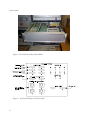
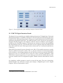
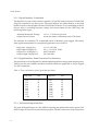
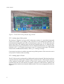
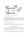
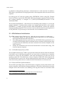
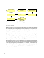
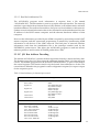
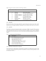
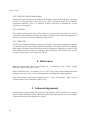
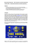
An Auxiliary Interface Instrumentation Module for
the AMRL Low Speed Wind Tunnel Data
Acquisition System
F. J. Bird
Air Operations Division
Aeronautical and Maritime Research Laboratory
DSTO-TR-1215
ABSTRACT
An IBM PC based electronic module is described which extends the capability of the data
acquisition system of the Low Speed Wind Tunnel (LSWT) at the Aeronautical and
Maritime Research Laboratory (AMRL). Occasions arise when wind tunnel measurements
require external data input or specific data extraction by external or temporarily acquired
equipment. Access to the data is provided by the Auxiliary Data Module (ADM). The
ADM is one of the VME modules in the LSWT instrumentation console.
The functions of two types of plug-in commercial board are used to provide a suite of
digital input and output functions using a total of three boards. Two input, two output
and two tachometer channels are provided by two identical I/O boards in addition to the
two standard PC RS-232C serial communication ports. The second plug-in board type
provides eight analog input channels and two analog output channels with 12 bit
resolution.
RELEASE LIMITATION
Approved for public release
Published by
DSTO Aeronautical and Maritime Research Laboratory
506 Lorimer St
Fishermans Bend, Victoria 3207 Australia
Telephone: (03) 9626 7000
Fax: (03) 9626 7999
© Commonwealth of Australia 2001
AR-012-026
October 2001
APPROVED FOR PUBLIC RELEASE
An Auxiliary Interface Instrumentation Module
for the AMRL Low Speed Wind Tunnel Data
Acquisition System
Executive Summary
An electronic module called the Auxiliary Data Module (ADM) is described which
provides the functions required to enable external data input or specific data extraction
from the LSWT data acquisition system. The ADM is a PC based unit configured to
mechanically conform to the existing console appearance and VME mounting
requirements. The module is accessable to the Master computer via the LSWT ethernet
network
Auxiliary data may consist of input signals from additional transducers, or data extracted
for recording on external devices, or control signals to carry out a remote task.
The ADM provides a suite of user interfaces which include two 16 bit digital input ports,
two 16 bit digital output ports, and two dedicated digital input ports for the measurement
of tachometer data from powered propellors on wind tunnel models.
In addition, the ADM includes a plug-in analog interface board which provides eight
differential analog input channels and two output channels. These analog functions are
able to be reconfigured manually by using switches and links on the board for the
selection of input and output voltage range and polarity options. All analog I/O channels
have 12 bit resolution.
Authors
F.J. Bird
Air Operations Division
____________________
Fred Bird is a Senior Officer (Technical) Grade C who has
qualifications equivalent to Certificate of Technology. He has worked
in AMRL for 15 years and for Air Operations Division for the last 5
years. He has extensive experience in Data Acquisition in the wind
tunnel and Navy helicopter and ship trial environments. He has more
recently been involved in human factor research in helicopter night
operations.
________________________________________________
Contents
1. INTRODUCTION ............................................................................................................... 1
2. MODULE HARDWARE .................................................................................................... 1
2.1 PXB-721 Digital Interface Board. ........................................................................... 3
2.1.1 Digital Interface Connection ....................................................................... 4
2.1.2 Digital Interface Panel Connector Pin Functions ..................................... 4
2.1.3 Tachometer Input Interface......................................................................... 4
2.1.4 Digital Port Connector Allocation.............................................................. 5
2.2 PC-74LA Analog Interface Board........................................................................... 5
2.2.1 PC-74LA Board Configuration System...................................................... 5
2.2.2 Analog Input Sub-system............................................................................ 6
2.2.3 Analog Input Circuit ................................................................................... 6
2.2.4 Analog Output Sub-system......................................................................... 7
2.3 Network Interface Card (NIC)................................................................................ 7
3. MODULE SOFTWARE ...................................................................................................... 7
3.1 ADM Software Initialisation.................................................................................. 8
3.1.1 3C5X9PD Packet Driver TSR....................................................................... 8
3.1.2 Date and Time Synchronisation. ................................................................ 8
3.1.3 Downloading an Initialisation File............................................................. 9
3.2 ADM General Operation......................................................................................... 9
3.2.1 Initialisation of the AUXILARY program. ................................................ 9
3.2.1.1 The Log File. ............................................................................................. 10
3.2.1.2 Read the Initialisation File...................................................................... 11
3.3 PC I/O Bus Address Decoding ........................................................................... 11
3.4 PXB-721 Board Configuration .............................................................................. 12
3.5 PC-74LA Board Configuration ............................................................................. 12
3.5.1 PC-74LA Register Structure ...................................................................... 12
3.5.2 ADGCR ........................................................................................................ 13
3.5.3 ADCSR ......................................................................................................... 13
3.5.4 ADDAT/DADAT0 (Low Bytes)............................................................... 13
3.5.5 ADDAT/DADT0 (High Bytes)................................................................. 14
3.5.6 DADAT1 ...................................................................................................... 14
3.5.7 TMRCTR ...................................................................................................... 14
4. REFERENCES..................................................................................................................... 14
5. ACKNOWLEDGEMENTS............................................................................................... 14
DSTO-TR-1215
1. Introduction
The Auxiliary Data Module (ADM) provides a suite of interface facilities which provide
access to data for non standard external monitoring or processing equipment for the Low
Speed Wind Tunnel (LSWT) at the Aeronautical and Maritime Research Laboratory
(AMRL). The suite includes two digital input ports, two digital output ports, eight analog
input ports, two analog output ports, two standard serial communication ports and two
additional digital input ports dedicated to tachometer data available from wind tunnel
models with powered propellers.
The digital ports are provided by two identical re-configurable commercial plug-in boards.
The analog ports are provided by a further commercial plug-in board. The serial ports are
the COM 1 and COM 2 ports of the IBM PC platform which is used as a basis for the
module.
The ADM operating software consists of C++ version 3.1 modules with the support of the
multi-tasking program Real Time Kernel (RTK) version 4.5.
2. Module hardware
The ADM is based on a standard IBM PC chassis which has been modified to be contained
within VME physical module size standards. Figure 1 shows the module installation.
The usual PC power ON/OFF switching is retained but concealed behind a VME standard
panel. Mains power is routed via the module’s cooling fan tray which contains the main
accessable power switch for the module. This is the normal arrangement for the LSWT
data acquisition system.
The interface functions are carried out by commercial plug in boards. Digital I/O uses two
identical configurable PXB-721 interface boards. The analog functions use a single PC74LA analog interface board. Serial communication is conducted using the PC Com ports
COM1 and COM2.
A 3COM Etherlink3 ethernet adapter board is used to interface the module to the LSWT
ethernet providing accessibility for the master computer.
User interface connections are made on the Auxiliary Interface connector field mounted on
a panel at the rear of the VME rack system. Extension cabling connects the panel
connectors to the respective interface plug-in boards within the ADM. Figure 2 shows the
user connector panel with basic functional explanations. Figure 3 shows the appearance of
the panel as seen in the LSWT control room.
1
DSTO-TR-1215
Figure 1: The LSWT Auxiliary Data Module
Figure 2: Auxiliary Interface Connector Panel
2
DSTO-TR-1215
Figure 3: Visual Appearance of the Auxiliary Interface Connector Panel.
2.1 PXB-721 Digital Interface Board.
The digital I/O port interface provided by this board consists of 72 digital lines. The board
design groups these as a number of 8 bit ports. The 8 bit ports are accessed in pairs as 16
bit ports in the ADM operating software. The ports are provided by three Intel 8255 digital
interfacing integrated circuits (IC)1 per PXB-721 board. The IC devices are mounted on
daughter boards plugged to the respective PXB-721 board. In addition, each daughter
board has an I/O header connector. The headers are referred to as H1 to H6 parallelling
the designations of the ICs. The fact that there are two separate PXB-721 boards means
there are six 8255 ICs in all. This report refers to these as IC1 to 3 on Board 1 and IC4 to 6
on Board 2.
Each 8255 IC has three 8 bit ports referred to as A, B & C. The module accesses an A and a
B port to make a 16 bit port on each of IC1, 2, 3 & 4 to form the two 16 bit input digital
ports and the two 16 bit output digital ports. IC5 & IC6 are used to provide the tachometer
input ports. Port A of IC5 and Port A of IC6 are used to provide Tachometer 1 and
Tachometer 2 inputs respectively. IC port setting up is done by the ADM software. Data
bytes are written to the IC configuration register. Details of this are described in Section
3.4.
For simplicity, polled operation is used to access all the ports. The user of Auxiliary
Module digital I/O will refer to these ports simply as Digital Input 1 and 2, Digital
Output 1 and 2 or Tachometer 1 and 2.
1
Intel Microprocessor and Peripheral Handbook Vol.II 1989
3
DSTO-TR-1215
2.1.1 Digital Interface Connection
The Digital I/O ports on the connector panel are 37 pin D37 male connectors. Female D37
plugs are required to use these ports. The panel sockets are cabled directly to the 8255
header sockets on the daughter boards of each PXB-721 board. To avoid damage to the IC
devices due to exceeding absolute voltage and current limits for the 8255 chips, the
following limits apply.
Absolute Maximum Voltage:
Output Drive Current:
-0.5 to +7 Volts wrt ground.
4 mA, this infers a minimum load of 750 ohms.
The interface is nominally TTL compatible and it is therefore quite rugged. The steady
state signal characteristics for peripheral application are as follows:
Input Low voltage (VIL)
Input High Voltage(VIH)
Output Low Voltage(VOL)
Output High Voltage(VOH)
-0.5 to 0.8 Volts
2.0 to +5 ± 10% Volts
0.45 Volts Max.
2.4 Volts Min.
2.1.2 Digital Interface Panel Connector Pin Functions
The pin functions of the Digital I/O include digital signal lines and ground reference lines.
Table 1 lists the pin numbers and their functions which are applicable to all the Digital
I/O D37 connectors.
Table 1. The pin allocations of the Digital Interface Panel
Dig.Line
D0
D1
D2
D3
D4
D5
D6
D7
Gnd
Pin
Dig.Line
Pin
1
20
2
21
3
22
4
23
5
D8
D9
D10
D11
D12
D13
D14
D15
Gnd
14
33
15
34
16
35
17
36
32
2.1.3 Tachometer Input Interface
The only dedicated function of the ADM is acquiring the model tachometer signals. The
8255 IC chips IC5 and IC6 are used for this purpose. The D37 connectors on the connection
4
DSTO-TR-1215
panel designated 5 and 6 are connected to these ICs through headers H5 and H6. The D37
connector pin allocation is identical to Table 1 for the digital I/O functions.
The tachometer signals consist of four digit binary coded decimal (BCD) values. The
numbers are serialised at the transmitting ends of the tachometer input signal
transmission lines. Each value is received as a serial set of four digits. Each digit is
represented as a four bit binary number. The values are converted to hexadecimal values
and passed to the Module database via the RTK tasks ModelTacho1 and ModelTacho2 which
form part of the ADM operating software.
The tachometer signals are cabled to the connector panel from the model in the test section
of the wind tunnel and appear on two additional D37 sockets. These signals are linked to
the digital I/O input connectors 5 and 6 of the panel using external ribbon link cables on
the external face of the connector panel, which is shown in Figure 3.
2.1.4 Digital Port Connector Allocation
The panel connectors allocated to the Digital I/O Ports are listed in Table 2.
Table 2. Allocation of Digital Input/Output Ports.
Digital Port
Digital In 1
Digital In 2
Digital Out 1
Digital Out 2
Tachometer 1
Tachometer 2
Connector (D37)
1
2
3
4
5
6
2.2 PC-74LA Analog Interface Board.
2.2.1 PC-74LA Board Configuration System
Configuration of this system board is achieved partly by hardware link positions and by
software commands which place specific values into board registers. Figure 4 shows the
PC74LA plug-in board.
5
DSTO-TR-1215
Figure 4: The PC74LA Analog Interface plug-in board
2.2.2 Analog Input Sub-system.
The Analog to Digital Converter (ADC) subsystem consists of a monolithic Integrated
Circuit (IC) capable of providing 12 bit conversion for 16 multiplexed channels. An
instrumentation amplifier with software selectable gain values of 1, 10, 100, 500 isolates the
input of the ADC. The ADM program sets the pre-amplifier gain to 1 as a default value.
Physical links select input characteristics such as: 8 differential channels or 16 single ended
channels; ±2.5 V , ±5 V bipolar input range or a 0 to 5 V unipolar input range. The default
selections are 8 Differential channels, with a ±5 V analog I/O range.
Conversion is continuous, and the program uses polled operation. The conversion rate is
set by the PC-74 timer software setting.
2.2.3 Analog Input Circuit
The PC-74LA board is configured for 8 differential analog channels. The board must have
a ground reference which is provided through a resistor of value 7.5 K from the outer line
of the insulated coaxial BNC connector to the board’s analog ground. This ground is
extended from the PC-74LA board I/O header connector to the connector panel by the
ribbon extender cables from within the ADM module. The circuit arrangement is shown in
Figure 5.
6
DSTO-TR-1215
Figure 5: Ground Reference Circuit for the Analog Input Function
2.2.4 Analog Output Sub-system.
Two Digital to Analog Conversion (DAC) ICs provide the two channels of analog output
with 12 bit resolution. The output range is hardware selectable. Selections available are
±5V, ±2.5V and 0 to 5V. The bipolar ±5V option is selected as the default value. The
linearity of this sub-system is nominally 0.01% FSR. The Analog output channels are
available at two insulated BNC coaxial sockets on the connector panel marked as “Analog
Output 1 and 2”.
2.3 Network Interface Card (NIC)
The ethernet board used for the wind tunnel modules based on the PC platform is the
3COM Etherlink III board. The interrupt level for the ADM ethernet handling is IRQ11.
3. Module Software
The operating software consists of C++ version 3.0 modules supported by modules of the
multitasking program Real Time Kernel (RTK) version 4.5. The C++ modules include
functions to control database access and the plug-in boards, and they use manufacturer’s
library modules where appropriate.
The C modules are all required to be entered in the C++ project file, AUXILARY.prj, as are
library files pertaining to the multi-tasking Real Time Kernel. RTK enables programmers
7
DSTO-TR-1215
to minimise waiting during interrupts, communications or other activities. In addition,
RTK allows a prioritisation of the program tasks so that important tasks are carried out as
required.
On start-up the PC loads the packet driver PKTDRVR.C before using File Transfer
Protocol (FTP) to copy the file AUXILARY.INI from the master computer. Following this,
the working directory is changed to C:\LSWT\SOFTWARE\AUXILARY to run
AUXILARY.EXE.
The module DB_HNDLR.C calls functions for handling data transfers to or from the
module database. Communication packets are formed and decoded by the module
PKTDRVR.C. A further program module called ENETDRVR.C contains the ethernet
interrupt handling segments. It also receives vector words from the host, passing these on
to DB_HNDLR.C for processing to form the index for host database access.
3.1 ADM Software Initialisation.
The ADM operates in the following way. After the power is turned on or after reset;
1.
The module, being a PC, goes through all the normal power-on self testing and
then loads MS DOS from the hard drive.
2.
The ADM specific functions performed by AUTOEXEC.BAT commands are to
load the 3C5X9PD Packet Driver terminate and stay resident (TSR) program, then
to synchronise the ADM date and time with that of the master computer on the
LSWT network.
3.
Finally the initialisation file named AUXILARY.INI is downloaded using FTP
from the master computer.
3.1.1 3C5X9PD Packet Driver TSR.
The 3C5X9PD Packet Driver2 TSR is a program that makes the ethernet Network Interface
Card (NIC) easy for MS DOS programs to use. It provides a consistent set of interface
functions to access the NIC hardware. Each NIC manufacturer provides the drivers
specific to their NIC. The ADM uses a 3Com Company 3C509 NIC which requires the
3CX9PD TSR driver from 3Com. All the ADM programs which make use of the ethernet
network use this packet driver to send and receive information over the network.
3.1.2 Date and Time Synchronisation.
The modules providing data to the LSWT master computer are all synchronised to the
master computer’s date and time during initialisation. This allows data packets to be time
stamped. It also allows easier cross checking of the log files written to a module’s hard
More information can be obtained on Packet Drivers from the FAQ at
http://seagull.rtd.com/pub/tcpip/other-faqs/pktdrv.faq
2
8
DSTO-TR-1215
disk against data files written to the master computer’s disk, should that be required. The
program PDTSTNET uses the packet driver to send packets to the master computer that
ask for the current date and time.
The information returned by the master computer is for UTC and must be corrected by a
factor of +10 hours to the local time zone at AMRL, Melbourne (AEST). If daylight saving
is in operation, the correction is +11 hours. Once the correction is applied PDTSTNET sets
the DOS clock to the local time equivalent of the master computer’s date and time.
3.1.3 Downloading an Initialisation File.
The master computer partly controls each LSWT Data Acquisition System module’s
operation through the initialisation files. Much of the ADM operation is controlled by
information in a file named AUXILARY.INI. This file is downloaded during every ADM
initialisation so that the copy on the ADM hard disk is always up to date with the master
file held on the disk of the master computer. The File Transfer Protocol (FTP) is used to
reliably copy the file over the network to the ADM disk. The program FTP uses the packet
driver to access the network and takes commands from the file FTPINI.CMD in the
\LSWT\SOFTWARE\AUXILARY\ directory. These commands enable it to log into the
master computer, change to the net/ini directory, and download the AUXILARY.INI file
which becomes the latest AUXILARY.INI on the ADM disk. The contents of the
AUXILARY.INI file, are dealt with later in Section 3.2 on the main ADM program.
3.2 ADM General Operation.
Once the initialisation phase of the AUTOEXEC.BAT file has been done, general operation
of the ADM is controlled by the AUXILARY.EXE program. This program also provides the
data in the database to any computer on the network that requests it.
Two methods of making the data available to computers external to the ADM are possible.
A direct request for an item of data from the database is the first method. The second
method is known as “streaming mode”. Once the ADM is told to operate in streaming
mode it repeatedly broadcasts packets on the network containing all of the parameter data
in the local database. Any computer on the network can listen to the broadcast data and
make immediate use of it.
3.2.1 Initialisation of the AUXILARY program.
The initialisation process consists of recording any error messages in a log file and using
data stored in an information (.INI) file, setting up IP addresses for accessing by the master
computer and other modules. The initialisation process described in the following
paragraphs is depicted in Figure 6.
9
DSTO-TR-1215
Reset or Power
On
Start up Database
Handler
Start up Ethernet
Handler
Start Log File
Operation
Read in “Auxilary.ini”
Initialisation File
Set up Serial Port
Hardware
Start up Real Time
Kernel
End
of
Initialisation
Figure 6: Initialisation Sequence of the AUXILARY program.
3.2.1.1 The Log File.
When the AUXILARY program is started it immediately opens a file. Any error messages
are written to the file as well as to the screen. Since error messages on the screen are only
there for a short time, the file is a more permanent record of a problem or other notable
aspects of the ADM operation. The filename is made up from the current date and time
that the file is opened. Since date and time cannot be easily placed in a name limited to
eight characters the fields are encoded.
The first three letters are taken from the name of the instrumentation module so log files
from different modules can be archived in a common directory. In this case the first three
letters will be AUX. The next letter of the file name represents the month. This is encoded
in hexadecimal (ie base 16) so that January is 0(zero) and December is represented as B.
Letter number five in the file name is an encoded representation of the day in the month.
The first day of the month is denoted by 1 and day 31 by V.
Effectively, this is encoding to base 32 with an offset of 1. Letter number six in the filename
is a base 24 encoding of the hour of the day. The hour just after midnight is represented as
0 (zero) and the hour just before midnight (hour 23) as the letter N. Letter number 7 and
letter number 8 are grouped together to show the minute when the file was created. This is
not encoded. Minute zero is represented as 00 and minute 59 as 59. The extension for the
filename is set to LOG to denote a log file. To clarify this scheme “AUX12345.LOG” would
have been created on February 2nd at 3:45 AM. Likewise,”AUXBVN59.LOG” corresponds
to December 31st at 11:59 PM.
10
DSTO-TR-1215
3.2.1.2 Read the Initialisation File.
The AUXILARY program reads information it requires from a file named
”AUXILARY.INI”. The information is used to set up the network interface. The network
interface is provided with an Internet Protocol (IP) number, an IP address mask, and an IP
broadcast address. These allow the module to set up its own local address on the network.
Further network related information that is also obtained from the initialisation file is the
IP address of the LSWT master computer and the ethernet hardware address of that
computer.
However the information provided by the ADM is required by more than just the LSWT
master computer and this operational requirement is satisfied by broadcasting ADM
information to all devices on the LSWT network. The final piece of network interface
information read from the initialisation file is the interrupt number used by the
PKTDRVR.C packet driver. This allows the AUXILARY program to send and receive
ethernet packets to and from the 3C5X9PD packet driver TSR.
3.3 PC I/O Bus Address Decoding
The module AUXILARY.C operates the data acquisition boards to obtain auxiliary data.
The boards occupy bus I/O space using the addresses listed in Table 3 for data and port
control. The Module program uses the C function SETIOPORTS.C to pass control data to
the control registers. The function needs only the boards’ base addresses to do this. The
control data is defined in the program for each configuration required, ie output or input
for the respective ports.
Table 3. Board addresses for data and port control
PXB-721
Board 1 Base
Board 2 Base
Digital In 1
Base and Data Registers
Tachometer 1
Tachometer 2
210H
220H
210/218H High Byte
211/219H Low Byte
214H High Byte
215H Low Byte
218/224H High Byte
219/225H Low Byte
224/210H
228/220H
PC-74LA
Control and Data Registers
Status Reg. ADCSR
Gain.Chan. ADGCR
Conv. Data ADDATL
Conv. Data ADDATH
Dac0 In DADAT0L
Dac0 In DADAT0H
DAC1 In DADAT1L
DAC1 In DADAT1H
Timer Cont. TMRCTR
310H
311H
312H Low Byte
313H High Byte
312H Low Byte
313H High Byte
314H Low Byte
315H High Byte
317H
Digital In 2
Digital Out 1
11
DSTO-TR-1215
3.4 PXB-721 Board Configuration
Configuring the Digital ports to enable input or output functions is done by passing
defined values into the control register within each 8255 IC. This is a function of the
Module program AUXILARY.EXE. The Control register AT I/O bus addresses are listed in
Table 4.
Table 4: Digital Port addresses on the PXB-721 plug-in board.
IC Device
Register address
IC1
213H
IC2
217H
IC3
21BH
IC4
223H
IC5
227H
IC6
22BH
The configuration options are few. Since only ports A and B of each 8255 IC are to be
utilised, the configuration data is listed in Table 5.
Table 5: Configuration data for the Digital Ports.
Option
Data Value
A,B Input
9BH
A,B Output
80H
A Input
90H
The control registers are set to these values by calls to the C function SETIOPORTS in
AUXILARY.C.
3.5
PC-74LA Board Configuration
The PC-74LA board is configured by a combination of hardware links and program
actions. The hardware links are used to set base address, interrupt level, DMA level, DAC
output range, Differential or Single-ended input, and the ADC input range.
The hardware setup is considered as fixed. Should a change be required to accommodate a
special function in the future the operator is advised to refer to the PC-74LA User Manual.3
The PC-74LA board has eight registers to control aspects of configuration and data
handling. They are addressed by increments from the base address commencing with the
base address.
3.5.1 PC-74LA Register Structure
Eight locations starting with the Board base address in AT I/O space provide the
programmable registers of the PC-74LA Board. They are described in Table 6:
3
12
Interworld Electronics & Computer Industries (Aust) Pty Ltd
DSTO-TR-1215
Table 6. Register Locations of the PC-74LA Plug-in Board
Base Offset Title
0
1
2
3
4
5
6
7
`
ADCSR
ADGCR
ADDAT/DADAT0
ADDAT/DADAT0
DADAT1
DADAT1
DIOP1/DIOP2
TMRCTR
Function
AD Control/Status
AD Gain/Channel Selection
Low Byte ADC I/O Data
High Byte ADC I/O Data
Low Byte DAC1 Data
High Byte DAC1 Data
This port is unused
Clock Frequency select
3.5.2 ADGCR
The lower four bits of this register hold the required channel in binary form. Bits 6 and 7
hold the code for the gain required. Unity gain is set as default. Bits 4 and 5 are not used .
3.5.3 ADCSR
The Mode 0 is always the operation mode, no interrupt or DMA is required. The register is
read to determine the status of the ADC and if data is available. A write action is required
to clear bit 4 if a conversion error occurs. The content of the ADCSR register is described in
Table 7.
Table 7.
Content of the ADCSR Register.
Bit
Description
0
1
2
3
4
5
6
7
Bit 0 of Mode Selection (set as 0)
Bit 1 of Mode Selection (set as 0)
Interrupt Enable Bit (set as 0)
DMA Enable Bit (set as 0)
A/D Error Clear Bit (write 1 to clear)
A/D Busy Flag (during conversion)
Set on Conversion Error
Set on Conversion Completion
3.5.4 ADDAT/DADAT0 (Low Bytes)
This register has a dual function. During ADC operation it contains the low byte of the
conversion result. During DAT operation it contains the low byte of the input data word to
be loaded into DAC0.
13
DSTO-TR-1215
3.5.5 ADDAT/DADT0 (High Bytes)
This has the same functioning as ADDAT/DADAT0 except that the high byte of the data
is used. A read operation at the end of an ADC conversion clears the conversion
completed condition of bit 7 of ADCSR. A DAC conversion is initiated by a write
operation to this register.
3.5.6 DADAT1
This register holds the low byte of the 12 bit word to be loaded into DAC1 for a DAC
conversion and is addressed as base plus offset 4. DADAT1 also holds the high 4 bits of
the DAT conversion and this is addressed with offset 5.
3.5.7 TMRCTR
The PC-74LA internal clock has a frequency of 600 kH. This register enables the selection
of a suitable divider to provide the preferred frequency. There are 64 selections enabling a
wide range of divider values and therefore clock frequencies. Reference to the PC-74LA
User Manual is the best means of making a special selection. The default value for the
divider is 100 giving a clock frequency of 6 kH.
4. References
Quatech, Quatech PXB-721 User manual (Re7v. B)
Parkway. Akron, Ohio 44311, USA.
Quatech Inc., 662
Wolf
Ledges
Interworld Electronics, User Manual for PC-74 (First Ed.), 1988. Interworld Electronics &
Computer Ind. Aust. P/L., 933 Glenhuntly Road, Caulfield Sth., 3162, Australia.
Intel, Microprocessor and Peripheral Handbook Vol 2,
Avenue, Santa Clara, California, 95051, USA.
Intel Corporation, 3065 Bowers
5. Acknowledgements
I would like to acknowledge the assistance of M. Spataro and O. Holland for software
advice and the blending in of the ethernet modules, and I. Kerton who wrote the original
software modules for the digital port control.
14
OUTSIDE AUSTRALIA
ABSTRACTING AND INFORMATION ORGANISATIONS
Library, Chemical Abstracts Reference Service
Engineering Societies Library, US
Materials Information, Cambridge Scientific Abstracts, US
Documents Librarian, The Center for Research Libraries, US
INFORMATION EXCHANGE AGREEMENT PARTNERS
Acquisitions Unit, Science Reference and Information Service, UK
Library - Exchange Desk, National Institute of Standards and Technology, US
National Aerospace Laboratory, Japan
National Aerospace Laboratory, Netherlands
SPARES (5 copies)
Total number of copies:
64
Page classification: UNCLASSIFIED
DEFENCE SCIENCE AND TECHNOLOGY ORGANISATION
DOCUMENT CONTROL DATA
2. TITLE
An Auxiliary Interface Instrumentation Module for the AMRL
Low Speed Wind Tunnel Data Acquisition System
1. PRIVACY MARKING/CAVEAT (OF
DOCUMENT)
3. SECURITY CLASSIFICATION (FOR UNCLASSIFIED REPORTS
THAT ARE LIMITED RELEASE USE (L) NEXT TO DOCUMENT
CLASSIFICATION)
Document
Title
Abstract
(U)
(U)
(U)
4. AUTHOR(S)
5. CORPORATE AUTHOR
F. J. Bird
Aeronautical and Maritime Research Laboratory
506 Lorimer St
Fishermans Bend Victoria 3207 Australia
6a. DSTO NUMBER
6b. AR NUMBER
6c. TYPE OF REPORT
7. DOCUMENT DATE
DSTO-TR-1215
AR-012-026
Technical Report
October 2001
8. FILE NUMBER
9. TASK NUMBER
10. TASK SPONSOR
11. NO. OF PAGES
M1/9/743
RDI 98/179
DSTO
13
12. NO. OF
REFERENCES
3
13. URL on the World Wide
14. RELEASE AUTHORITY
http://www.dsto.defence.gov.au/corporate/reports/DSTO-TR-1215.pdf
Chief, Air Operations Division
15. SECONDARY RELEASE STATEMENT OF THIS DOCUMENT
Approved for public release
OVERSEAS ENQUIRIES OUTSIDE STATED LIMITATIONS SHOULD BE REFERRED THROUGH DOCUMENT EXCHANGE, PO BOX 1500, SALISBURY, SA 5108
16. DELIBERATE ANNOUNCEMENT
No Limitations
17. CASUAL ANNOUNCEMENT
18. DEFTEST DESCRIPTORS
Yes
Wind tunnel tests, Aerodynamics, Data Acquisition, Low speed wind tunnels, Modules
19. ABSTRACT
An IBM PC based electronic module is described which extends the capability of the data acquisition system
of the Low Speed Wind Tunnel (LSWT) at the Aeronautical and Maritime Research Laboratory (AMRL).
Occasions arise when wind tunnel measurements require external data input or specific data extraction by
external or temporarily acquired equipment. Access to the data is provided by the Auxiliary Data Module
(ADM). The ADM is one of the VME modules in the LSWT instrumentation console.
The functions of two types of plug-in commercial board are used to provide a suite of digital input and
output functions using a total of three boards. Two input, two output and two tachometer channels are
provided by two identical I/O boards in addition to the two standard PC RS-232C serial communication
ports. The second plug-in board type provides eight analog input channels and two analog output channels
with 12 bit resolution.
Page classification: UNCLASSIFIED