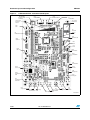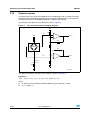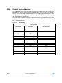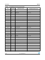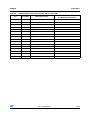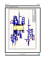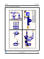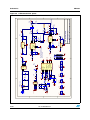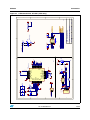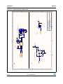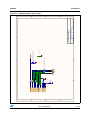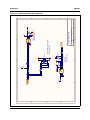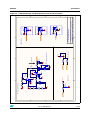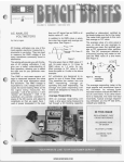
1
UM1564
User manual
STM32373C-EVAL evaluation board
Introduction
The STM32373C-EVAL evaluation board is designed as a complete demonstration and
development platform for STMicroelectronics’ ARM cortex-M4 core-based
STM32F373VCT6 microcontroller. It features two I2Cs, three SPIs, three USARTs, one
CAN, one CEC controller, one 12-bit ADC, three 16-bit sigma delta ADCs, three 12-bit
DACs, internal 32-KByte SRAM and 256-KByte Flash, touch sensing, USB FS, and JTAG
debugging support. This evaluation board can be used as a reference design for user
application development but it is not considered as the final application.
The full range of hardware features on the board can help the user evaluate all peripherals
(USB FS, USART, audio DAC, microphone ADC, color LCD, IrDA, LDR (light-dependent
resistor), MicroSD card, HDMI CEC, ECG (electrocardiogram), pressure sensor, CAN, IR
(infrared) transmitter and receiver, EEPROM, touch slider, temperature sensor, etc.) and
develop their own applications. Extension headers make it possible to easily connect a
daughterboard or wrapping board for a specific application.
An ST-LINK/V2 is integrated on the board as an embedded in-circuit debugger and
programmer for the STM32 MCU.
Figure 1.
STM32373C-EVAL evaluation board
Table 1.
Applicable tools
Type
Evaluation tools
September 2012
Part number
STM32373C-EVAL
Doc ID 023566 Rev 1
1/66
www.st.com
Contents
UM1564
Contents
1
2
2/66
Overview . . . . . . . . . . . . . . . . . . . . . . . . . . . . . . . . . . . . . . . . . . . . . . . . . . 6
1.1
Features . . . . . . . . . . . . . . . . . . . . . . . . . . . . . . . . . . . . . . . . . . . . . . . . . . . 6
1.2
Demonstration software . . . . . . . . . . . . . . . . . . . . . . . . . . . . . . . . . . . . . . . 6
1.3
Order code . . . . . . . . . . . . . . . . . . . . . . . . . . . . . . . . . . . . . . . . . . . . . . . . . 7
1.4
Delivery recommendations . . . . . . . . . . . . . . . . . . . . . . . . . . . . . . . . . . . . . 7
Hardware layout and configuration . . . . . . . . . . . . . . . . . . . . . . . . . . . . . 8
2.1
Development and debug support . . . . . . . . . . . . . . . . . . . . . . . . . . . . . . . 11
2.2
Power supply . . . . . . . . . . . . . . . . . . . . . . . . . . . . . . . . . . . . . . . . . . . . . . 12
2.3
Power modes . . . . . . . . . . . . . . . . . . . . . . . . . . . . . . . . . . . . . . . . . . . . . . 14
2.4
Clock sources . . . . . . . . . . . . . . . . . . . . . . . . . . . . . . . . . . . . . . . . . . . . . . 15
2.5
Reset source . . . . . . . . . . . . . . . . . . . . . . . . . . . . . . . . . . . . . . . . . . . . . . 16
2.6
Boot option . . . . . . . . . . . . . . . . . . . . . . . . . . . . . . . . . . . . . . . . . . . . . . . . 16
2.7
Audio . . . . . . . . . . . . . . . . . . . . . . . . . . . . . . . . . . . . . . . . . . . . . . . . . . . . 17
2.8
USB . . . . . . . . . . . . . . . . . . . . . . . . . . . . . . . . . . . . . . . . . . . . . . . . . . . . . 18
2.9
RS-232 and IrDA . . . . . . . . . . . . . . . . . . . . . . . . . . . . . . . . . . . . . . . . . . . 18
2.10
Touch sensing slider . . . . . . . . . . . . . . . . . . . . . . . . . . . . . . . . . . . . . . . . . 19
2.11
MicroSD card . . . . . . . . . . . . . . . . . . . . . . . . . . . . . . . . . . . . . . . . . . . . . . 20
2.12
RF EEPROM . . . . . . . . . . . . . . . . . . . . . . . . . . . . . . . . . . . . . . . . . . . . . . 20
2.13
EEPROM . . . . . . . . . . . . . . . . . . . . . . . . . . . . . . . . . . . . . . . . . . . . . . . . . 20
2.14
CAN . . . . . . . . . . . . . . . . . . . . . . . . . . . . . . . . . . . . . . . . . . . . . . . . . . . . . 21
2.15
HDMI CEC . . . . . . . . . . . . . . . . . . . . . . . . . . . . . . . . . . . . . . . . . . . . . . . . 21
2.16
IR transmitter and IR receiver . . . . . . . . . . . . . . . . . . . . . . . . . . . . . . . . . 22
2.17
Electrocardiogram demonstration . . . . . . . . . . . . . . . . . . . . . . . . . . . . . . 22
2.18
PT100 temperature sensor . . . . . . . . . . . . . . . . . . . . . . . . . . . . . . . . . . . . 23
2.19
Pressure sensor . . . . . . . . . . . . . . . . . . . . . . . . . . . . . . . . . . . . . . . . . . . . 26
2.20
Analog input . . . . . . . . . . . . . . . . . . . . . . . . . . . . . . . . . . . . . . . . . . . . . . . 28
2.21
Potentiometer . . . . . . . . . . . . . . . . . . . . . . . . . . . . . . . . . . . . . . . . . . . . . . 28
2.22
LDR . . . . . . . . . . . . . . . . . . . . . . . . . . . . . . . . . . . . . . . . . . . . . . . . . . . . . 29
2.23
Temperature sensor . . . . . . . . . . . . . . . . . . . . . . . . . . . . . . . . . . . . . . . . . 29
2.24
Display and input devices . . . . . . . . . . . . . . . . . . . . . . . . . . . . . . . . . . . . . 30
Doc ID 023566 Rev 1
UM1564
3
4
Contents
Connectors . . . . . . . . . . . . . . . . . . . . . . . . . . . . . . . . . . . . . . . . . . . . . . . 31
3.1
HDMI sink connector CN1 . . . . . . . . . . . . . . . . . . . . . . . . . . . . . . . . . . . . 31
3.2
HDMI source connector CN2 . . . . . . . . . . . . . . . . . . . . . . . . . . . . . . . . . . 31
3.3
RF EEPROM daughterboard connector CN3 . . . . . . . . . . . . . . . . . . . . . . 32
3.4
CAN D-type 9-pin male connector CN5 . . . . . . . . . . . . . . . . . . . . . . . . . . 32
3.5
MicroSD connector CN7 . . . . . . . . . . . . . . . . . . . . . . . . . . . . . . . . . . . . . . 33
3.6
Sigma Delta ADC connector CN9 . . . . . . . . . . . . . . . . . . . . . . . . . . . . . . 33
3.7
SAR ADC DAC connector CN10 . . . . . . . . . . . . . . . . . . . . . . . . . . . . . . . 34
3.8
SAR ADC DAC connector CN11 . . . . . . . . . . . . . . . . . . . . . . . . . . . . . . . 34
3.9
RS-232 connector CN12 . . . . . . . . . . . . . . . . . . . . . . . . . . . . . . . . . . . . . 35
3.10
Daughterboard extension connectors CN13 and CN14 . . . . . . . . . . . . . . 36
3.11
ETM Trace debugging connector CN15 . . . . . . . . . . . . . . . . . . . . . . . . . . 40
3.12
User USB type B connector CN16 . . . . . . . . . . . . . . . . . . . . . . . . . . . . . . 40
3.13
JTAG/SWD debugging connector CN17 . . . . . . . . . . . . . . . . . . . . . . . . . . 41
3.14
Power connector CN18 . . . . . . . . . . . . . . . . . . . . . . . . . . . . . . . . . . . . . . 41
3.15
ST-LINK/V2 programming connector CN19 . . . . . . . . . . . . . . . . . . . . . . . 42
3.16
TFT LCD connector CN20 . . . . . . . . . . . . . . . . . . . . . . . . . . . . . . . . . . . . 42
3.17
Audio jack CN21 . . . . . . . . . . . . . . . . . . . . . . . . . . . . . . . . . . . . . . . . . . . . 42
3.18
ST-LINK/V2 USB type B connector CN22 . . . . . . . . . . . . . . . . . . . . . . . . 42
Schematics . . . . . . . . . . . . . . . . . . . . . . . . . . . . . . . . . . . . . . . . . . . . . . . 43
Appendix A STM32373C-EVAL pinout . . . . . . . . . . . . . . . . . . . . . . . . . . . . . . . . . 60
Appendix B Mechanical dimensions. . . . . . . . . . . . . . . . . . . . . . . . . . . . . . . . . . . 64
5
Revision history . . . . . . . . . . . . . . . . . . . . . . . . . . . . . . . . . . . . . . . . . . . 65
Doc ID 023566 Rev 1
3/66
List of tables
UM1564
List of tables
Table 1.
Table 2.
Table 3.
Table 4.
Table 5.
Table 6.
Table 7.
Table 8.
Table 9.
Table 10.
Table 11.
Table 12.
Table 13.
Table 14.
Table 15.
Table 16.
Table 17.
Table 18.
Table 19.
Table 20.
Table 21.
Table 22.
Table 23.
Table 24.
Table 25.
Table 26.
Table 27.
Table 28.
Table 29.
Table 30.
Table 31.
Table 32.
Table 33.
Table 34.
Table 35.
Table 36.
Table 37.
4/66
Applicable tools. . . . . . . . . . . . . . . . . . . . . . . . . . . . . . . . . . . . . . . . . . . . . . . . . . . . . . . . . . . 1
Third-party toolchain support . . . . . . . . . . . . . . . . . . . . . . . . . . . . . . . . . . . . . . . . . . . . . . . 11
Power-related jumpers . . . . . . . . . . . . . . . . . . . . . . . . . . . . . . . . . . . . . . . . . . . . . . . . . . . . 12
Power mode related jumpers . . . . . . . . . . . . . . . . . . . . . . . . . . . . . . . . . . . . . . . . . . . . . . . 14
Low voltage limitations . . . . . . . . . . . . . . . . . . . . . . . . . . . . . . . . . . . . . . . . . . . . . . . . . . . . 14
8-MHz crystal (X2-related solder bridge) . . . . . . . . . . . . . . . . . . . . . . . . . . . . . . . . . . . . . . 15
32-KHz crystal (X1-related solder bridge). . . . . . . . . . . . . . . . . . . . . . . . . . . . . . . . . . . . . . 15
Boot-related switches . . . . . . . . . . . . . . . . . . . . . . . . . . . . . . . . . . . . . . . . . . . . . . . . . . . . . 16
Boot0-related jumper . . . . . . . . . . . . . . . . . . . . . . . . . . . . . . . . . . . . . . . . . . . . . . . . . . . . . 17
Audio-related jumpers. . . . . . . . . . . . . . . . . . . . . . . . . . . . . . . . . . . . . . . . . . . . . . . . . . . . . 17
RS-232- and IrDA-related jumpers . . . . . . . . . . . . . . . . . . . . . . . . . . . . . . . . . . . . . . . . . . . 18
Touch sensing slider-related solder bridges . . . . . . . . . . . . . . . . . . . . . . . . . . . . . . . . . . . . 19
EEPROM-related jumpers . . . . . . . . . . . . . . . . . . . . . . . . . . . . . . . . . . . . . . . . . . . . . . . . . 20
CAN-related jumpers . . . . . . . . . . . . . . . . . . . . . . . . . . . . . . . . . . . . . . . . . . . . . . . . . . . . . 21
Jumpers of the ECG amplifier. . . . . . . . . . . . . . . . . . . . . . . . . . . . . . . . . . . . . . . . . . . . . . . 22
Temperature sensor voltage range. . . . . . . . . . . . . . . . . . . . . . . . . . . . . . . . . . . . . . . . . . . 24
PT100-related jumper . . . . . . . . . . . . . . . . . . . . . . . . . . . . . . . . . . . . . . . . . . . . . . . . . . . . . 25
Temperature sensor related solder bridge . . . . . . . . . . . . . . . . . . . . . . . . . . . . . . . . . . . . . 29
LCD modules . . . . . . . . . . . . . . . . . . . . . . . . . . . . . . . . . . . . . . . . . . . . . . . . . . . . . . . . . . . 30
HDMI sink connector CN1 . . . . . . . . . . . . . . . . . . . . . . . . . . . . . . . . . . . . . . . . . . . . . . . . . 31
HDMI source connector CN2 . . . . . . . . . . . . . . . . . . . . . . . . . . . . . . . . . . . . . . . . . . . . . . . 32
RF EEPROM daughterboard connector CN3 . . . . . . . . . . . . . . . . . . . . . . . . . . . . . . . . . . . 32
CAN D-type 9-pin male connector CN5 . . . . . . . . . . . . . . . . . . . . . . . . . . . . . . . . . . . . . . . 32
MicroSD connector CN7 . . . . . . . . . . . . . . . . . . . . . . . . . . . . . . . . . . . . . . . . . . . . . . . . . . . 33
Sigma Delta ADC connector CN9. . . . . . . . . . . . . . . . . . . . . . . . . . . . . . . . . . . . . . . . . . . . 33
SAR ADC DAC connector CN10 . . . . . . . . . . . . . . . . . . . . . . . . . . . . . . . . . . . . . . . . . . . . 34
SAR ADC DAC connector CN11 . . . . . . . . . . . . . . . . . . . . . . . . . . . . . . . . . . . . . . . . . . . . 34
RS-232 connector CN12 with HW flow control and ISP support . . . . . . . . . . . . . . . . . . . . 35
Daughterboard extension connector CN13 . . . . . . . . . . . . . . . . . . . . . . . . . . . . . . . . . . . . 36
Daughterboard extension connector CN14 . . . . . . . . . . . . . . . . . . . . . . . . . . . . . . . . . . . . 38
ETM Trace debugging connector CN15 . . . . . . . . . . . . . . . . . . . . . . . . . . . . . . . . . . . . . . . 40
User USB type B connector CN16 . . . . . . . . . . . . . . . . . . . . . . . . . . . . . . . . . . . . . . . . . . . 40
JTAG/SWD debugging connector CN17 . . . . . . . . . . . . . . . . . . . . . . . . . . . . . . . . . . . . . . 41
USB type B connector CN22 . . . . . . . . . . . . . . . . . . . . . . . . . . . . . . . . . . . . . . . . . . . . . . . 42
STM32373C-EVAL pinout . . . . . . . . . . . . . . . . . . . . . . . . . . . . . . . . . . . . . . . . . . . . . . . . . 60
STM32373C mechanical dimensions . . . . . . . . . . . . . . . . . . . . . . . . . . . . . . . . . . . . . . . . . 64
Document revision history . . . . . . . . . . . . . . . . . . . . . . . . . . . . . . . . . . . . . . . . . . . . . . . . . 65
Doc ID 023566 Rev 1
UM1564
List of figures
List of figures
Figure 1.
Figure 2.
Figure 3.
Figure 4.
Figure 5.
Figure 6.
Figure 7.
Figure 8.
Figure 9.
Figure 10.
Figure 11.
Figure 12.
Figure 13.
Figure 14.
Figure 15.
Figure 16.
Figure 17.
Figure 18.
Figure 19.
Figure 20.
Figure 21.
Figure 22.
Figure 23.
Figure 24.
Figure 25.
Figure 26.
Figure 27.
Figure 28.
Figure 29.
Figure 30.
Figure 31.
Figure 32.
Figure 33.
Figure 34.
Figure 35.
Figure 36.
Figure 37.
Figure 38.
STM32373C-EVAL evaluation board . . . . . . . . . . . . . . . . . . . . . . . . . . . . . . . . . . . . . . . . . . 1
Hardware block diagram . . . . . . . . . . . . . . . . . . . . . . . . . . . . . . . . . . . . . . . . . . . . . . . . . . . . 9
STM32373C-EVAL evaluation board layout . . . . . . . . . . . . . . . . . . . . . . . . . . . . . . . . . . . 10
Temperature measurement schematic diagram . . . . . . . . . . . . . . . . . . . . . . . . . . . . . . . . . 23
Pressure measurement schematic diagram . . . . . . . . . . . . . . . . . . . . . . . . . . . . . . . . . . . . 26
STM32373C-EVAL potentiometer . . . . . . . . . . . . . . . . . . . . . . . . . . . . . . . . . . . . . . . . . . . 28
STM32373C-EVAL LDR . . . . . . . . . . . . . . . . . . . . . . . . . . . . . . . . . . . . . . . . . . . . . . . . . . . 29
HDMI sink connector CN1 (front view) . . . . . . . . . . . . . . . . . . . . . . . . . . . . . . . . . . . . . . . . 31
HDMI source connector CN2 (front view) . . . . . . . . . . . . . . . . . . . . . . . . . . . . . . . . . . . . . . 31
RF EEPROM daughterboard connector CN3 (front view) . . . . . . . . . . . . . . . . . . . . . . . . . 32
CAN D-type 9-pin male connector CN5 . . . . . . . . . . . . . . . . . . . . . . . . . . . . . . . . . . . . . . . 32
MicroSD connector CN7 . . . . . . . . . . . . . . . . . . . . . . . . . . . . . . . . . . . . . . . . . . . . . . . . . . . 33
Sigma Delta ADC connector CN9 (top view) . . . . . . . . . . . . . . . . . . . . . . . . . . . . . . . . . . . 33
SAR ADC DAC connector CN10 (top view) . . . . . . . . . . . . . . . . . . . . . . . . . . . . . . . . . . . . 34
SAR ADC DAC connector CN11 (top view) . . . . . . . . . . . . . . . . . . . . . . . . . . . . . . . . . . . . 34
RS-232 connector CN12 (front view) . . . . . . . . . . . . . . . . . . . . . . . . . . . . . . . . . . . . . . . . . 35
ETM Trace debugging connector CN15 (top view). . . . . . . . . . . . . . . . . . . . . . . . . . . . . . . 40
User USB type B connector CN16 (front view) . . . . . . . . . . . . . . . . . . . . . . . . . . . . . . . . . . 40
JTAG/SWD debugging connector CN17 (top view) . . . . . . . . . . . . . . . . . . . . . . . . . . . . . . 41
Power supply connector CN18 (front view) . . . . . . . . . . . . . . . . . . . . . . . . . . . . . . . . . . . . 41
USB type B connector CN22 (front view) . . . . . . . . . . . . . . . . . . . . . . . . . . . . . . . . . . . . . . 42
Schematic diagram of STM32373C-EVAL . . . . . . . . . . . . . . . . . . . . . . . . . . . . . . . . . . . . . 44
STM32373C-EVAL MCU . . . . . . . . . . . . . . . . . . . . . . . . . . . . . . . . . . . . . . . . . . . . . . . . . . 45
STM32373C-EVAL audio . . . . . . . . . . . . . . . . . . . . . . . . . . . . . . . . . . . . . . . . . . . . . . . . . . 46
STM32373C-EVAL peripherals . . . . . . . . . . . . . . . . . . . . . . . . . . . . . . . . . . . . . . . . . . . . . 47
STM32373C-EVAL power . . . . . . . . . . . . . . . . . . . . . . . . . . . . . . . . . . . . . . . . . . . . . . . . . 48
STM32373C-EVAL ST-LINK (JTAG only) . . . . . . . . . . . . . . . . . . . . . . . . . . . . . . . . . . . . . 49
STM32373C-EVAL JTAG and Trace . . . . . . . . . . . . . . . . . . . . . . . . . . . . . . . . . . . . . . . . . 50
STM32373C-EVAL RS-232 and IrDA . . . . . . . . . . . . . . . . . . . . . . . . . . . . . . . . . . . . . . . . . 51
STM32373C-EVAL HDMI_CEC . . . . . . . . . . . . . . . . . . . . . . . . . . . . . . . . . . . . . . . . . . . . . 52
STM32373C-EVAL LCD and SD card . . . . . . . . . . . . . . . . . . . . . . . . . . . . . . . . . . . . . . . . 53
STM32373C-EVAL CAN and IR . . . . . . . . . . . . . . . . . . . . . . . . . . . . . . . . . . . . . . . . . . . . . 54
STM32373C-EVAL Touch slider. . . . . . . . . . . . . . . . . . . . . . . . . . . . . . . . . . . . . . . . . . . . . 55
STM32373C-EVAL I2C peripherals . . . . . . . . . . . . . . . . . . . . . . . . . . . . . . . . . . . . . . . . . . 56
STM32373C-EVAL PT100 temperature sensor and connectors . . . . . . . . . . . . . . . . . . . . 57
STM32373C-EVAL ECG and pressure sensor. . . . . . . . . . . . . . . . . . . . . . . . . . . . . . . . . . 58
MB989 LCD daughter . . . . . . . . . . . . . . . . . . . . . . . . . . . . . . . . . . . . . . . . . . . . . . . . . . . . . 59
STM32373C mechanical dimensions . . . . . . . . . . . . . . . . . . . . . . . . . . . . . . . . . . . . . . . . . 64
Doc ID 023566 Rev 1
5/66
Overview
UM1564
1
Overview
1.1
Features
●
1.2
Four 5-V power supply options:
–
Power jack
–
ST-LINK/V2 USB connector
–
User USB connector
–
Daughterboard
●
I2S audio DAC and stereo audio jack
●
2-Gbyte or more SPI interface MicroSD card
●
I2C compatible serial interface temperature sensor, EEPROM, and RF EEPROM (dual
interface EEPROM)
●
RS-232 communication
●
IrDA transceiver
●
JTAG/SWD and ETM trace debug support, ST-LINK/V2 embedded
●
240x320 TFT color LCD connected to SPI interface
●
Joystick with 4-directional control and selector
●
Reset, wakeup or tamper and key button
●
4 color user LEDs and 2 LEDs as MCU power range indicators
●
ECG, pressure sensor, and PT100 temperature sensor connected to 16-bit sigma delta
ADC of the STM32F373VCT6
●
Extension connectors for daughterboard or wrapping board
●
Microcontroller voltage choice: 3.3 V or adjustable from 2.0 V to 3.6 V
●
USB FS connector
●
Touch slider
●
RTC with backup battery
●
CAN2.0A/B compliant connection
●
Light-dependent resistor (LDR)
●
Two HDMI connectors with DDC (display data channel) and CEC
●
IR transmitter and receiver
●
Two ADC and DAC input and output signal connectors and one sigma delta ADC input
signal connector
●
Potentiometer
Demonstration software
Demonstration software is preloaded on the board’s Flash memory for easy demonstration
of the device peripherals in standalone mode. For more information and to download the
latest version available, please refer to the STM32373C-EVAL demonstration software
available on www.st.com.
6/66
Doc ID 023566 Rev 1
UM1564
1.3
Overview
Order code
To order the STM32F373VCT6 evaluation board, use the order code STM32373C-EVAL.
1.4
Delivery recommendations
Some verification of the board is needed before using it for the first time to make sure that
nothing was damaged during shipment and that no components are unplugged or lost.
When the board is extracted from its plastic bag, please check that no component remains
in the bag.
The main components to verify are:
1.
The 8-MHz crystal (X2) which may have been removed by a shock from its socket.
2.
The MicroSD card which may have been ejected from the connector CN7 (right side of
the board).
3.
The dual-interface EEPROM board (ANT7-M24LR-A) which may have been unplugged
from the connector CN3 (top left corner of the board).
For all information concerning the version of the MCU used on the board, its specification
and possible related limitations, please visit www.st.com to download the relevant data
sheet and erratasheet.
Caution:
There is an explosion risk if the battery is replaced by an incorrect one. Make sure to
dispose of used batteries according to the instructions.
Doc ID 023566 Rev 1
7/66
Hardware layout and configuration
2
UM1564
Hardware layout and configuration
The STM32373C-EVAL evaluation board is designed around the STM32F373VCT6 (100pin LQFP package). The hardware block diagram, Figure 2, illustrates the connection
between the STM32F373VCT6 and the peripherals (color LCD, touch slider, USB FS
connector, temperature sensor, USART, IrDA, audio, EEPROM, RF EEPROM, MicroSD
card, and embedded ST-LINK). Figure 3 illustrates how to locate these features on the
actual evaluation board. Features described in Section 2.1 to Section 2.24 below are shown
in Figure 3.
8/66
Doc ID 023566 Rev 1
UM1564
Figure 2.
Hardware layout and configuration
Hardware block diagram
Joystick
LEDs
RS232
transceiver
GPIO
Wakeup,
tamper
.
button
Photo-R
USART
Voltage
translator
USART2
connector
IrDA
transceiver
STM32F373VCT6
Embedded
ST-LINK/V2
Comparator
USB type B
connector
JTAG
Touch slider
TS controller
2-pin
connector
DAC/ADC
JTAG and
trace
connector
Micro SD
card
SPI3
USB
connector
USB FS
CAN driver
and
connector
CAN
CEC
IR transmitter
and
IR receiver
Dot matrix
LCD
HDMI connector
IRTIM PWM
EEPROM
GpAMP2
I2C
Potentiometer
RF EEPROM
connector
Temperature
sensor
ADC
PT100
temp. sensor
Voltage
translator
I2S
SD ADC
Pressure
sensor and
amplifier
SD ADC
DAC
ECG sensor
and amplifier
SD ADC
ADC
Speaker
amplifier
2.0 V to 3.6 V
adjustable
regulator
3.3 V regulator
Extension
connector for
GPIOs
Amplifier
Microphone
MS30560V1
Doc ID 023566 Rev 1
9/66
Hardware layout and configuration
Figure 3.
UM1564
STM32373C-EVAL evaluation board layout
CN3
RF EEPROM
daughter board
connector
CN2
HDMI SOURCE
CN1
HDMI SINK
S1
Touch Slider
CN13,CN14
Extension
header
TS1 & TS2
ECG Probe
CN5
CAN
U5
Pressure
Sensor
U9
STM32F373VCT6
CN7
MicroSD card
CN12
USART2
R63
LDR
U12
IrDA
CN16
USB FS
CN15
ETM TRACE
CN17
JTAG/SWD
U22
IR transmitter
LD10
IR LED
CN18
Power Jack
U28
Microphone
CN22
ST-LINK/V2
USB
CN21
Audio jack
LD7
ST-LINK/V2
COM LED
RV2
VDD_Adjustment
RV 3
VDD range
Potentiometer LEDs
B1
Reset Key
4 colors
LEDS
B2
Tamper
Button
U34
Joystick
B3
Key
Button
MS30561V1
10/66
Doc ID 023566 Rev 1
UM1564
2.1
Hardware layout and configuration
Development and debug support
Version 2 of the ST-LINK (ST-LINK/V2) is embedded on the board. This tool allows onboard
program loading and debugging of the STM32F373VCT6 using the JTAG or SWD interface.
Third-party debug tools are also supported using the JTAG/SWD connector (CN17) or the
ETM trace connector (CN15).
A specific driver needs to be installed on your PC for communication with the embedded
ST-LINK/V2. The install shield, called ST-LINK_V2_USBdriver.exe, is available from the ST
website. To download and install this driver, please refer to the software and development
tools page of the STM32F family on www.st.com.
Third-party toolchains, Atollic TrueSTUDIO, KEIL ARM-MDK, IAR EWARM, and Tasking
VX-Toolset support ST-LINK/V2 according to Table 2.
Table 2.
Third-party toolchain support
Toolchain
Version
Atollic TrueSTUDIO
2.1
Keil MDK-ARM
4.20
IAR EWARM
6.20
Altium TASKING VX-Toolset
4.0.1
Connect the embedded ST-LINK/V2 to the PC via a standard USB cable from connector
CN22. The bi-color LED LD7 (COM in Figure 3) indicates the status of the communication
as follows:
Note:
●
Slow blinking red/off: at power-on before USB initialization
●
Fast blinking red/off: after the first correct communication between the PC and
STLink/V2 (enumeration).
●
Red LED on: when initialization between the PC and ST-LINK/V2 is successfully
finished.
●
Green LED on: after successful target communication initialization
●
Blinking red/green: during communication with target
●
Red on: communication finished and OK
●
Orange on: communication failure
It is possible to power the board via CN22 (embedded ST-LINK/V2 USB connector) even if
an external tool is connected to CN15 (ETM trace connector) or CN17 (external JTAG and
SWD connector).
Remove R29, R73, and R89 when using the ETM 4-bit function. In this situation, the touch
slider and joystick do not work.
Doc ID 023566 Rev 1
11/66
Hardware layout and configuration
2.2
UM1564
Power supply
STM32373C-EVAL evaluation board is designed to be powered by a 5 V DC power supply
and is protected by PolyZen U26 from damage caused by overvoltage and overcurrent fault
conditions. It is possible to configure the evaluation board to use any of following four power
supply sources:
●
5-V DC power adapter connected to CN18, the power jack on the board (see Power
Supply Unit (PSU) in Figure 3). The external power supply is not provided with the
board.
●
5-V DC power with 500 mA limitation from CN22, the type-B USB connector of STLINK/V2 (see STlk 5-V power source in Figure 3).
●
5-V DC power with 500 mA limitation from CN16, the type-B USB connector (see U5V
5-V power source in Figure 3).
●
5-V DC power from CN13 and CN14, the extension connector for the daughterboard
(see D5V for daughterboard in Figure 3).
The power supply is configured by setting the related jumpers JP10, JP11, JP12, and JP13
as described in Table 3 below.
Table 3.
Power-related jumpers
Jumper
Description
035
34LK
035
34LK
035
34LK
56
035
34LK
$6
56
035
34LK
Doc ID 023566 Rev 1
$6
12/66
56
For power supply from the power supply jack (CN18) to both
STM32373C -EVAL and daughterboard connected on CN13 &
CN14, JP10 is set as shown to the right:
Note: the daughterboard must not have its own power supply
connected.
$6
For power supply from the daughterboard connectors (CN13
and CN14) to STM32373C-EVAL only, JP10 is set as shown to
the right:
56
For power supply from the USB connector (CN16) to
STM32373C-EVAL only, JP10 is set as shown to the right:
$6
JP10
(selects one of
the four possible
power supply
resources)
56
For power supply from the USB connector of ST-LINK/V2
(CN22) to STM32373C-EVAL only, JP10 is set as shown to the
right:
$6
For power supply from the power supply jack (CN18) to the
STM32373C-EVAL only, JP10 is set as shown to the right:
Jumper setting
UM1564
Hardware layout and configuration
Table 3.
Jumper
JP11
JP12
JP13
Note:
Power-related jumpers (continued)
Description
Jumper setting
Vbat is connected to a battery when JP11 is set as shown to
the right:
1 2 3
Vbat is connected to the VDD power when JP11 is set as
shown to the right:
This is the default setting.
1 2 3
VDD is connected to a fixed 3.3-V DC power supply when
JP12 is set as shown to the right:
This is the default setting.
1 2 3
VDD is connected to an adjustable DC power supply from 2.0
V to 3.6 V when JP12 is set as shown to the right:
1 2 3
VDDA power is connected to VDD when JP13 is set as shown
to the right:
This is the default setting.
1 2 3
VDDA power is connected to a fixed 3.3-V DC power supply
when JP13 is set as shown to the right:
1 2 3
VDD is adjustable from 2.0 V to 3.6 V. However, to take component tolerance into account
and to guarantee that VDD does not exceed the chip range specification, VDD is ideally
designed to be adjusted from 2.1 V to 3.5 V on the board.
JP17 is connected with the VDDA power supply and the SD_VREF+ pin of the
microcontroller. The default setting is closed. When the SD_VREF+ pin needs an extended
reference level, please open JP17 and connect the extended reference to pin 1 (the top pin
of JP17).
LED LD8 is lit (red) when the STM32373C-EVAL evaluation board is powered by a 5-V DC
power supply. LED LD6 is lit (red) when the microcontroller is powered by VDD < 2.4 V (low
voltage). LED LD5 is lit (green) when the microcontroller is powered by
VDD > 2.4 V
Doc ID 023566 Rev 1
13/66
Hardware layout and configuration
2.3
UM1564
Power modes
A total of three power modes are supported on the board and can be configured by setting
the related jumpers JP12 and JP13 as described below in Table 4. The power modes are as
follows:
●
Power mode 1: VDD and VDDA are connected together and powered by a fixed 3.3-V
DC power supply.
●
Power mode 2: VDD and VDDA are connected together and powered by an adjustable
voltage that ranges from 2.0 V to 3.6 V.
●
Power mode 3: VDD is powered by an adjustable voltage that ranges from 2.0 V to
3.6 V while VDDA is powered by a fixed 3.3-V DC power supply.
Table 4.
Power mode related jumpers
Power mode configuration
Power mode
Microcontroller IDD
measurement(1)
JP12
JP13
1 2 3
1 2 3
OK
1 2 3
1 2 3
Not allowed
Power mode 2
1 2 3
1 2 3
OK
Power mode 3
1 2 3
1 2 3
Not allowed
Power mode 1
1. To measure the IDD of the microcontroller, use a current meter mounted on JP15 (which must be open).
JP16 must also be open to disconnect VDDA from any analog power (VDD_ANA) connected to the analog
circuit.
Table 5 shows the low voltage limitations that might apply depending on the characteristics
of some peripheral components. Components might work incorrectly when the power level
is lower than the limitation.
Table 5.
14/66
Low voltage limitations
Peripheral
Component
IO name
Low voltage
limitation
USB
CN16
USB
3V
MicroSD card
CN7
SPI3
2.7 V
CAN
CN5
CAN
3V
Doc ID 023566 Rev 1
UM1564
Hardware layout and configuration
Note:
The recommended AC220 V to DC5 V power adapter is PSU-5V2A. It is not included with
the board but can be ordered from ST as a separate item. You can also use another
equivalent 5 V power adapter (polarity compatible with CN18) to power the STM32373CEVAL board via the CN18 power jack on the board. To order the recommended power
supply, use order code PSU-5V2A.
2.4
Clock sources
Two clock sources are available on the STM32373C-EVAL evaluation board for use with the
STM32F373VCT6 microcontroller and embedded real-time clock (RTC). They are:
●
8-MHz crystal (X2) with socket clock source for the STM32F373VCT6 microcontroller.
It can be removed from the socket when an internal RC clock is used (see Table 6).
●
32-KHz crystal (X1) for use with an embedded RTC (see Table 7).
Table 6.
8-MHz crystal (X2-related solder bridge)
Solder bridge
Description
When SB23 is open, PF0 is connected to the 8-MHz crystal oscillator.
This is the default setting.
SB23
When SB23 is closed, PF0 is connected to the extension connector CN14. In this
case, C18 and the X2 pin must be removed to avoid disturbance due to the 8-Mhz
quartz.
When SB24 is open, PF1 is connected to the 8-MHz crystal oscillator.
This is the default setting.
SB24
When SB24 is closed, PF1 is connected to the extension connector CN14. In this
case R38 must be removed to avoid disturbance due to the 8-Mhz quartz.
Table 7.
32-KHz crystal (X1-related solder bridge)
Solder bridge
SB25
Description
When SB25 is open, PC14 is connected to the 32-KHz crystal oscillator.
This is the default setting.
When SB25 is closed, PC14 is connected to the extension connector CN13. In this
case, R36 must be removed to avoid disturbance due to the 32-Khz quartz.
SB26
When SB26 is open, PC15 is connected to 32-KHz crystal.
This is the default setting.
When SB26 is closed, PC15 is connected to the extension connector CN13. In this
case, R37 must be removed to avoid disturbance due to the 32-Khz quartz.
Doc ID 023566 Rev 1
15/66
Hardware layout and configuration
2.5
UM1564
Reset source
The reset signal of the STM32373C-EVAL evaluation board is “low active” and the reset
sources (see Figure 3) include:
●
Reset button B1
●
Debugging tools from JTAG/SWD connector CN17 and ETM trace connector CN15
●
daughterboard from CN14
●
Embedded ST-LINK/V2
●
RS-232 connector CN12 for ISP (in-situ programming)
Note:
See Section 2.9: RS-232 and IrDA to change jumper JP7 when performing a reset. This is
handled by pin 8 of the RS-232 connector CN12 (clear to send (CTS) signal).
2.6
Boot option
The STM32373C-EVAL evaluation board is able to boot from:
●
Embedded user Flash
●
System memory with boot loader for ISP
●
Embedded SRAM for debugging
The boot option is configured by setting switch SW1 (BOOT0) and the User Option Bytes
bit12 (BOOT1) in the small information block (SIF). BOOT0 can also be configured via the
RS-232 connector CN12.
Table 8.
Boot-related switches
Bit12 in User
Option Bytes
Boot source
STM32373C-EVAL boot from User Flash when SW1 and bit12 in the
User Option Bytes are set as shown to the right.
This is the default setting.
X
STM32373C-EVAL boot from Embedded SRAM when SW1 and bit12
in the User Option Bytes are set as shown to the right.
0
STM32373C-EVAL boot from System Memory when SW1 and bit12 in
the User Option Bytes are set as shown to the right.
1
16/66
Doc ID 023566 Rev 1
Switch
configuration
37
37
37
UM1564
Hardware layout and configuration
Table 9.
2.7
Boot0-related jumper
Jumper
Description
JP9
When JP9 is closed, the Bootloader_BOOT0 is managed by pin 6 of connector
CN12 (RS-232 DSR signal). This configuration is used for boot loader application
only.
This is the default setting: it is not fitted.
Audio
The STM32373C-EVAL evaluation board supports stereo audio playback by an audio DAC
CS43L22 connected to the I2S port and one channel of the STM32F373VCT6 DAC. The
microphone is connected to the ADC input of STM32F373VCT6 through a microphone
amplifier.
I2C communication depends on the settings of jumpers JP4 and JP5:
Table 10.
Jumper
Description
JP4
PA9 is connected to the I2C2_SCL_5V signal on the audio DAC,
temperature sensor, RF EEPROM, and HDMI source connector
when JP4 is set as shown to the right:
This is the default setting.
JP5
Note:
Audio-related jumpers
Jumper setting
1 2 3
PA9 is connected to the I2C2_F_SCL signal on the EEPROM
when JP4 is set as shown to the right:
1 2 3
PA10 is connected to the I2C2_SDA_5V signal on the audio
DAC, temperature sensor, RF EEPROM, and HDMI source
connector when JP5 is set as shown to the right:
This is the default setting.
1 2 3
PA10 is connected to the I2C2_F_SDA signal on the EEPROM
when JP5 is set as shown to the right:
1 2 3
The I2C address of CS43L22 is 0b1001010.
The audio reset is connected with PD11 which is powered by the VDDA domain. When the
voltage of VDDA is not the same as the voltage of VDD (see Power mode 3 in Section 2.3),
the signal voltages are translated by divider resistance, R79 and R103, to avoid harming the
Audio Codec Chip U19.
Doc ID 023566 Rev 1
17/66
Hardware layout and configuration
2.8
UM1564
USB
STM32373C-EVAL evaluation board supports USB2.0 compliant, full-speed communication
via a USB type B connector (CN16). The evaluation board can be powered by this USB
connection at 5 V DC with 500 mA current limitation.
USB disconnection simulation can be implemented by controlling an external 1.5 KΩ pull-up
resistor on the USB+ line. The pull-up function can be enabled by PC5.
The USB operates correctly when VDD > 3 V.
2.9
RS-232 and IrDA
RS-232 (with hardware flow control clear to send (CTS) and request to send (RTS)) and
IrDA communication are supported by:
●
D-type 9-pin RS-232 connector (CN12)
●
IrDA transceiver (U12)
They are connected to USART2 of the STM32F373VCT6 on the STM32373C-EVAL
evaluation board. The Bootloader_RESET signal (which is shared with the CTS signal) and
the Bootloader_BOOT0 signal which is shared with the demand signal repository (DSR)
signal) are added on the RS-232 connector, CN12, for ISP support.
Table 11.
Jumper
Description
Jumper setting
1 2 3
JP6
USART2_RX is connected to the RS-232 transceiver and RS232 communication is enabled when JP6 is set as shown to the
right:
This is the default setting.
USART2_RX is connected to the IrDA transceiver and IrDA
communication is enabled when JP6 is set as shown to the
right:
1 2 3
USART2_CTS is connected to the RS-232 transceiver when
JP7 is set as shown to the right:
This is the default setting.
1 2 3
Bootloader_RESET is connected to the RS-232 transceiver
when JP7 is set as shown to the right:
1 2 3
JP7
18/66
RS-232- and IrDA-related jumpers
Doc ID 023566 Rev 1
UM1564
2.10
Hardware layout and configuration
Touch sensing slider
STM32373C-EVAL evaluation board supports a touch sensing slider based on either
resistor-capacitor (RC) charging or charge transfer technology. The charge transfer
technology is enabled by default assembly.
Table 12.
Touch sensing slider-related solder bridges
Solder bridge
SB8
Description
When SB8 is open, PD15 is connected to the sampling capacitor.
This is the default setting.
When SB8 is closed, PD15 is connected to the extension connector CN14. In this
case, C7 must be removed to avoid disturbance due to the capacitor.
SB9
When SB9 is open, PD14 is connected to the touch slider.
This is the default setting.
When SB9 is closed, PD14 is connected to the extension connector CN14. In this
case, R11 must be removed to avoid disturbance due to the touch slider
SB10
When SB10 is open, PD13 is connected to the touch slider.
This is the default setting.
When SB10 is closed, PD13 is connected to the extension connector CN14. In this
case, R12 must be removed to avoid disturbance due to the touch slider
SB11
When SB11 is open, PD12 is connected to the touch slider.
This is the default setting.
When SB11 is closed, PD12 is connected to the extension connector CN14. In this
case, R13 must be removed to avoid disturbance due to the touch slider
R93
When R93 is un-mounted, PE4 is connected to the touch slider.
This is the default setting.
When R93 is mounted, PE4 is connected to the extension connector CN13. In this
case, R31 must be removed to avoid disturbance due to the shield.
R95
When R95 is un-mounted, PE5 is connected to the slider.
This is the default setting.
When R95 is mounted, PE5 is connected to the extension connector CN13. In this
case, R82 must be removed to avoid disturbance due to the capacitor.
Note:
The touch slider is only fully functional when the STM32373C-EVAL is powered on Power
mode 1 (both VDD and VDDA are connected to a fixed 3.3 V power supply). When the
STM32373C-EVAL is powered on Power mode 2, it may be necessary to adjust the
capacitor value of C123 and the firmware so they are adapted to a voltage range of 2.0 V to
3.6 V of VDD. The touch slider is not functional when the STM32373C-EVAL is powered on
Power mode 3 because some IOs are also powered by the VDDA domain.
Doc ID 023566 Rev 1
19/66
Hardware layout and configuration
2.11
UM1564
MicroSD card
The 2-Gbyte (or more) MicroSD card connected to the SPI3 port (which is shared with the
color LCD) of the STM32F373VCT6 is available on the evaluation board. It can be enabled
by the chip select signal (PE2). This signal should be set as an open-drain output pin in the
STM32F373VCT6. MicroSD card detection is managed by the standard IO port PE3.
The MicroSD card operates correctly when VDD > 2.7 V.
2.12
RF EEPROM
The RF EEPROM daughterboard, ANT7-M24LR-A, is mounted on CN3 of the
STM32F373VCT6 via the I2C2 bus (which is shared with the temperature sensor U14,
audio codec U19, and DDC on the HDMI_Source connector CN2). The RF EEPROM can
be accessed by the microcontroller via the I2C2 bus or by radio frequency (RF) using a
13.56 MHz reader (for example, CR95HF).
The I2C address of the RF EEPROM daughterboard is 0b1010000.
I2C2 communication depends on the settings of jumper JP4 and JP5 as shown in Table 10:
Audio-related jumpers.
2.13
EEPROM
To fit Fast mode requirements, a 1-Mbit EEPROM, M24M01-HR, is directly connected to the
I2C2 bus of the STM32F373VCT6 by setting jumper JP4 and JP5 as shown in Table 10:
Audio-related jumpers.
Table 13.
EEPROM-related jumpers
Jumper
JP14
JP4, JP5
20/66
Description
When JP14 is closed, the EEPROM is in Write protection mode.
This is the default setting: it is not fitted.
Refer to Table 10: Audio-related jumpers.
Doc ID 023566 Rev 1
UM1564
2.14
Hardware layout and configuration
CAN
The STM32373C-EVAL evaluation board supports one channel of CAN2.0A/B complaint
CAN bus communication based on a 3.3-V CAN transceiver. High-speed mode, Standby
mode, and Slope control mode are available and can be selected by setting JP3.
Table 14.
CAN-related jumpers
Jumper
JP3
Description and jumper setting
The CAN transceiver operates in Standby mode when JP3 is set
as shown to the right:
1 2 3
The CAN transceiver operates in High-speed mode when JP3 is
set as shown to the right:
This is the default setting.
1 2 3
The CAN transceiver operates in Slope control mode when JP3 is open.
JP2
When JP2 is fitted, the CAN terminal resistor is enabled.
Default setting: not fitted.
CAN operates correctly when VDD > 3 V.
2.15
HDMI CEC
Two HDMI connectors, CN1 and CN2, are available on the STM32373C-EVAL evaluation
board.
●
●
Connector CN1 is a HDMI sink connector with:
–
DDC connected to I2C1 of the STM32F373VCT6
–
HPD controlled by IO PE0 through transistor T1
–
CEC connected to PB8 through transistor T2
Connector CN2 is an HDMI source connector with:
–
DDC connected to I2C2 (and shared with the temperature sensor, RF EEPROM,
and audio codec) of the STM32F373VCT6 by setting jumper JP4 and JP5 as
shown in Table 10: Audio-related jumpers.
–
HPD controlled by IO PD7
–
CEC connected to PB8 through transistor T2
–
HDMI 5-V powered by power switch U1
The signals TDMS D+[0:2], TDMS_CLK+, TDMS D-[0:2], and TDMS_CLK- are connected
together on these two HDMI connectors.
CEC injector mode can be enabled (for debugging purposes only) as follows:
●
Remove resistors R120, R172, R173, R174, R175, R213, and R221.
●
Close solder bridges SB1, SB2, SB3, and SB4.
Doc ID 023566 Rev 1
21/66
Hardware layout and configuration
UM1564
Note:
The I/O PE0 must be set in open-drain output mode by firmware when working as an HPD
signal control on the HDMI sink connector CN1.
2.16
IR transmitter and IR receiver
The IR receiver, TSOP34836, is connected to PB5 of the STM32F373VCT6 and the IR
transmitter is driven by PB9 through transistors T6 and T7 on the evaluation board.
The IR transmitter may be driven directly by PB9 when SB28 is closed and R240 is
removed.
2.17
Electrocardiogram demonstration
The electrocardiogram (ECG) demonstration is implemented on the STM32373C-EVAL
evaluation board. There are two ECG electrodes, TS1 and TS2, on the board for fingers
from the right and left hands of the human body. The first stage of the ECG amplifier circuit
is an instrument amplifier INA333 (U2). The gain is set to 5. The gain of the second amplifier
stage (U3A) is set to 10 or 40. The total gain of the circuit outside the microcontroller is set
to 50 or 200. The output of the amplifier is connected to the sigma delta ADC in the
STM32F373VCT6 through PE12.
Jumper JP1 can change the second stage amplifier gain (see Table 15).
Table 15.
Jumpers of the ECG amplifier
Jumper
JP1
Description
When JP1 is closed, the second amplifier gain is changed from 10 to 40.
Default setting: fitted.
A low-pass filter is available on the evaluation board but, by default, it is not used. This filter
is made of a second order Sallen-Key Low-pass Filter (U3C) having unitary gain and 9 Hz
cut-off frequency. It can be used in noisy environments to improve 50 Hz or 60 Hz noise
rejection.
This filter is enabled by removing R14 and soldering 0 Ω on the R183 footprint.
Caution is needed for ECG detection and heartbeat measurement. The recommendations
are:
22/66
1.
Humid air and fingers
2.
Large area in contact with the electrodes
3.
Relaxed body with no movement
4.
Digital (and or) analog filtering to improve 50 Hz or 60 Hz noise rejection
5.
Third electrode usage connected to GND
6.
Evaluation board preferably powered by USB
7.
Body must be electrically isolated from earth
Doc ID 023566 Rev 1
UM1564
2.18
Hardware layout and configuration
PT100 temperature sensor
There is a current source circuit on the STM32373C-EVAL evaluation board to provide a
fixed 1 mA current (when VDD = 3.3 V) to the platinum probe PT100 (R30). The R30 voltage
level is directly applied to the sigma delta ADC of the STM32F373VCT6, through PE7, to
measure the temperature value on PT100.
For temperatures lower than 100 °C, the resistor value is given by Equation 1.
Equation 1
R PT100 = 100 + 0.385 × T
T is the temperature in degrees Celsius.
The principle of the PT100 temperature sensor measurement is given in Figure 4.
Figure 4.
Temperature measurement schematic diagram
R4 = R
R3 = R
TSV631A
+
VDD
A1
R ref
R1 = 2R
R ref = VDD/2
TSV631A
R5 = R
+
A2
R2 = 2R
ADC IN
R PT100
VDD
VADC
VRref = VDD/2
VRref
R1 = 2R
=
R
R2 = 2R
MS30569V1
The operational amplifier, A1, and the resistors R1 to R5 form a differential amplifier with a
differential gain (GA1).
Due to the resistor values chosen, GA1 is equal to 1. This is known because the resistor
bridge, R1 and R2, connected to VDD is equivalent to the VDD/2 generator where R1/2 = R
internal resistor.
The voltage on Rref is given in Equation 2 to Equation 5.
Doc ID 023566 Rev 1
23/66
Hardware layout and configuration
UM1564
Equation 2
V OUTA1 = V REF + V OUTA2 (since G A1 = 1 )
Equation 3
V OUTA2 = V PT100
Equation 4
V REF = V OUTA1 – V PT100
Equation 5
V Rref = V ref = VDD ⁄ 2
The voltage on the ADC input is given in Equation 6.
Equation 6
V ADC = V PT100 = V Rref × R PT100 ⁄ R ref = R PT100 × VDD ⁄ ( 2 × R ref )
The measured PT100 value given by the ADC is shown in Equation 7.
Equation 7
R PT100 = [ V ref_ADC × N ⁄ ( 2
16
– 1 ) ] × 2 × R ref ⁄ ( VDD )
Where:
●
N is the value returned by the ADC corresponding to the voltage measured.
●
Vref_ADC is the ADC reference voltage (SD_VREF+ in Figure 26).
If Vref_ADC = VDD, the RPT100 value becomes as shown in Equation 8.
Equation 8
R PT100 = [ N ⁄ ( 2
16
– 1 ) ] × 2 × R ref
Conclusion
When the JP17 jumper is closed and the external reference voltage selected (Vref_ADC)
equals VDD, the temperature measurement becomes VDD independent.
Table 16 shows the voltage range corresponding to different temperatures for the ADC IN of
the STM32F373VCT6 where gain = 16.
Table 16.
Temperature sensor voltage range
VDD = 3.3 V
Rref = 1.8 KΩ
24/66
Temperature (°C)
Resistance (Ω)
Voltage (mV)
Vin ADC (V)
0
100
100
1.6
20
107.7
107.7
1.7
50
119.2
119.2
1.9
Doc ID 023566 Rev 1
UM1564
Note:
Hardware layout and configuration
A 100 Ω 0.1% resistor, R121, is used to calibrate PT100 by setting JP18.
Table 17.
Jumper
PT100-related jumper
Description and jumper setting
The 100-ohm 0.1% resistor is connected for calibration when
JP18 is set as shown to the right:
1 2 3
PT100 resistor is connected to measure temperature when JP18
is set as shown to the right:
This is the default setting.
1 2 3
JP18
Note:
The temperature result measured from PT100 is slightly higher than ambient temperature
due to board heat.
Doc ID 023566 Rev 1
25/66
Hardware layout and configuration
2.19
UM1564
Pressure sensor
An absolute pressure sensor with 1000 HP, full scale MPX2102, and an analog front end is
implemented on the STM32373C-EVAL board. The output differential pair is connected to
the sigma delta ADC in the STM32F373VCT6 via PE8 (P) and PE9 (N).
The principle of the pressure measurement is given in Figure 5.
Figure 5.
Pressure measurement schematic diagram
VDD
VIN+
R3
+
VDD
V OUT+
-
R2
R1
MPX2102
R2
-
VIN-
V TEMP
+
V OUT-
R3
R4
MS30570V1
The differential voltage, at output, of the amplifier is given in Equation 9.
Equation 9
V OUT+ – V OUT- = ( V IN+ – V IN- ) × ( G + R2 ⁄ R3 ) – VDD × R2 ⁄ R3
where:
26/66
●
G represents the operational amplifier differential gain when R3 is infinite.
●
G = 2 * R2/R1 + 1
Doc ID 023566 Rev 1
UM1564
Hardware layout and configuration
The operational amplifier differential input voltage provided by the pressure sensor is given
in Equation 10.
Equation 10
V IN+ – V IN- = P m × K × VDD
Where:
●
Pm = the pressure measured
●
K = sensitivity of the sensor (40 mV for VDD = 10 V and 1000 HPa)
The ADC output is related to the differential voltage by Equation 11.
Equation 11
V ADC = V ref_ADC × N ⁄ ( 2
16
– 1 ) = [ P m × K × VDD × ( G + R2 ⁄ R3 ) – VDD × R2 ⁄ R3 ] × G ADC
where:
●
N is the value returned by the ADC corresponding to the pressure measured
●
Vref_ADC is the ADC reference voltage (SD_VREF+ in Figure 26)
●
GADC is the ADC digital gain
So, if Vref_ADC = VDD Equation 11 becomes Equation 12.
Equation 12
N ⁄ (2
16
– 1 ) = [ P m × K × ( G + R2 ⁄ R3 ) – R2 ⁄ R3 ] × G ADC
Conclusion
Note:
1.
When the ADC external reference voltage is selected and JP17 jumper is closed,
Vref_ADC = VDD so the pressure measurement becomes VDD independent.
2.
The R2/R3 term in Equation 11 and Equation 12 allows the offset voltage
corresponding to atmospheric pressure to be partially reduced. Consequently, the
digital gain can be increased to improve sensitivity.
VTEMP may be used to compensate the temperature sensor drift by measuring the sensor
current change with temperature.
Doc ID 023566 Rev 1
27/66
Hardware layout and configuration
2.20
UM1564
Analog input
Three 2-pin connectors, CN9, CN10 and CN11, are connected to STM32F373VCT6 as
external analog inputs or DAC outputs.
CN9 connected to Sigma Delta ADC through PE11: a low-pass filter can be implemented for
the 2-pin connector by replacing R212 and C118 for ADC input with the right values of the
resistor and capacitor as required by end user’s application.
CN10 connected to ADC SAR input and DAC output through PA5: a low-pass filter can be
implemented for the 2-pin connector by replacing R42 and C21 for ADC input or replacing
R40 and C21 for DAC output with the right values of the resistor and capacitor as required
by end user’s application.
CN11 connected to ADC SAR input and DAC output through PA4: a low-pass filter can be
implemented for the 2-pin connector by replacing R45 and C26 for ADC input or replacing
R43 and C26 for DAC output with the right values of the resistor and capacitor as required
by end user’s application.
2.21
Potentiometer
A 10K ohm potentiometer RV3 is connected to comparator 2 through PA3 and ADC through
PB1 (default connection), as shown in Figure 6.
Figure 6.
STM32373C-EVAL potentiometer
ADC_SAR_AIN9
PB1
ADC_SD1_AIN3P-AIN2M
0
VDDA
GP comparator
RV3
0
GPCOMP2_IN+
PA3
NC
GPCOMP2_IN-
+
OUT
-
GND
Band gap 1.2 V
MS30943V1
28/66
Doc ID 023566 Rev 1
UM1564
2.22
Hardware layout and configuration
LDR
A light dependent resistor (LDR) is connected to ADC or comparator 1 through PA1, as
shown in Figure 7.
Figure 7.
STM32373C-EVAL LDR
VDDA
ADC_SAR_IN1
GP comparator
LDR_OUT
0
GPCOMP2_IN+
PA1
NC
LDR
GPCOMP2_IN-
+
OUT
-
Band gap 1.2 V
GND
MS30944V1
2.23
Temperature sensor
Temperature sensor STLM75M2E is connected to the I2C2 bus of STM32F373VCT6 when
jumpers JP4 and JP5 are set as shown in Table 10. It shares the same I2C2 bus with RF
EEPROM, Audio codec and DDC on the HDMI_Source connector.
I2C address of temperature sensor is 0b100100(A0). A0 can be 0 or 1 depending on the
setting of SB27.
Table 18.
Temperature sensor related solder bridge
Solder bridge
Description
I2C address A0 is 0 when SB27 is open (default setting).
SB27
I2C address A0 is 1 when SB27 is closed
Note:
The temperature result measured from STLM75M2E is slightly higher than ambient
temperature due to board heat.
Doc ID 023566 Rev 1
29/66
Hardware layout and configuration
2.24
UM1564
Display and input devices
The 240x320 TFT color LCD connected to port SPI3 of STM32F373VCT6 (shared with the
MicroSD card) and four general-purpose color LEDs (LD1, LD2, LD3, LD4) are available as
display devices. LED LD9 is connected with PA7 to show the status of comparator 2 when
debugging. The 4-direction joystick (U34) with selection wakeup button (B2) and key button
(B3) are available as input devices.
The LCD can be enabled by chip select signal PD2 and this signal should be set as opendrain output pin in STM32F373VCT6. All joystick signals should be set as pull-down input
pin in STM32F373VCT6.
Table 19.
LCD modules
TFT LCD CN20
30/66
Pin on CN20
Description
Pin connection
1
CS
PD2
2
SCL
PC10
3
SDI
PC12
4
RS
-
5
WR
-
6
RD
-
7
SDO
PC11
8
RESET
RESET#
9
VDD
3.3V
10
VCI
3.3V
11
GND
GND
12
GND
GND
13
BL_VDD
3.3V
14
BL_Control
3.3V
15
BL_GND
GND
16
BL_GND
GND
Doc ID 023566 Rev 1
UM1564
Connectors
3
Connectors
3.1
HDMI sink connector CN1
Figure 8.
HDMI sink connector CN1 (front view)
.47
Table 20.
HDMI sink connector CN1
Pin number
3.2
Description
Pin number
Description
1, 3, 4, 6, 7, 9,
10, 12
TMDS differential signal pair
connected to CN2
15
I2C1_SCL (PB6)
2, 5, 8, 11, 17
GND
16
I2C1_SDA (PB7)
13
CEC (PB8 through NMOS)
18
HDMI_5V_Sink
14
NC
19
HPD (PE0 through transistor)
HDMI source connector CN2
Figure 9.
HDMI source connector CN2 (front view)
.47
Doc ID 023566 Rev 1
31/66
Connectors
UM1564
Table 21.
HDMI source connector CN2
Pin number
3.3
Description
Pin number
Description
1, 3, 4, 6, 7, 9,
10, 12
TMDS differential signal pair
connected to CN1
15
I2C2_SCL (PA9)
2, 5, 8, 11, 17
GND
16
I2C2_SDA (PA10)
13
CEC (PB8 through NMOS)
18
HDMI_5V_Source from power
switch U1
14
NC
19
HPD (PD7)
RF EEPROM daughterboard connector CN3
Figure 10. RF EEPROM daughterboard connector CN3 (front view)
Table 22.
RF EEPROM daughterboard connector CN3
Pin number
3.4
Description
Pin number
Description
1
SDA (PA10)
3
+5 V
2
SCL (PA9)
4
GND
CAN D-type 9-pin male connector CN5
Figure 11. CAN D-type 9-pin male connector CN5
1 2 3 4 5
6 7 8 9
Front view
MS19140V2
Table 23.
CAN D-type 9-pin male connector CN5
Pin number
32/66
Description
Pin number
Description
1, 4, 8, 9
NC
7
CANH
2
CANL
3, 5, 6
GND
Doc ID 023566 Rev 1
UM1564
3.5
Connectors
MicroSD connector CN7
Figure 12. MicroSD connector CN7
Table 24.
MicroSD connector CN7
Pin number
3.6
Description
Pin number
Description
1
NC
6
Vss/GND
2
MicroSDcard_CS (PE2)
7
MicroSDcard_DOUT (PC11)
3
MicroSDcard_DIN (PC12)
8
NC
4
+3V3
9
GND
5
MicroSDcard_CLK (PC10)
10
MicroSDcard_detect (PE3)
Sigma Delta ADC connector CN9
Figure 13. Sigma Delta ADC connector CN9 (top view)
1
2
MS30945V1
Table 25.
Sigma Delta ADC connector CN9
Pin number
1
Description
AGND
Pin number
2
Doc ID 023566 Rev 1
Description
Sigma Delta ADC input PE11
33/66
Connectors
3.7
UM1564
SAR ADC DAC connector CN10
Figure 14. SAR ADC DAC connector CN10 (top view)
1
2
MS30945V1
Table 26.
SAR ADC DAC connector CN10
Pin number
1
3.8
Description
Pin number
AGND
2
Description
ADC-DAC input & output PA5
SAR ADC DAC connector CN11
Figure 15. SAR ADC DAC connector CN11 (top view)
1
2
MS30945V1
Table 27.
SAR ADC DAC connector CN11
Pin number
1
34/66
Description
GND
Pin number
2
Doc ID 023566 Rev 1
Description
ADC-DAC input & output PA4
UM1564
3.9
Connectors
RS-232 connector CN12
Figure 16. RS-232 connector CN12 (front view)
1 2 3 4 5
6 7 8 9
Front view
MS19140V2
Table 28.
RS-232 connector CN12 with HW flow control and ISP support
Pin number
Description
Pin number
Description
1
NC
6
Bootloader_BOOT0
2
RS232_RX (PD6)
7
RS232_RTS(PD4)
3
RS232_TX (PD5)
8
RS232_CTS(PD3)/Bootloader_RESET
4
NC
9
NC
5
GND
Doc ID 023566 Rev 1
35/66
Connectors
3.10
UM1564
Daughterboard extension connectors CN13 and CN14
Two 50-pins male header connectors CN13 and CN14 can be used to connect with
daughterboard or standard wrapping board to STM32373C-EVAL evaluation board. All
GPI/Os are available on them. The space between these two connectors and position of
power, GND and RESET pins are defined as a standard which allows to develop common
daughterboards for several evaluations boards.
The standard width between CN13 pin1 and CN14 pin1 is 2700 mils (68.58 mm). The
standard was implemented on the majority of evaluation boards. Each pin on CN13 and
CN14 can be used by a daughterboard after disconnecting it from the corresponding
function block on STM32373C-EVAL evaluation board. Please refer to Table 29 and
Table 30 for more details.
Table 29.
Pin
36/66
Daughterboard extension connector CN13
Description
Alternative function
How to disconnect from function block
on STM32373C-EVAL board
1
GND
-
-
3
PC7
I2S_CK
-
5
PC9
I2S_DIN
-
7
PA10
I2C2_SDA
Keep JP5 on open.
9
PA11
USB_DM
Remove R61.
11
PC14
OSC32_IN
Remove R36, close SB25.
13
PA13
SWDAT/JTMS
Disconnect CN15, CN17.
15
PC15
OSC32_OUT
Remove R37, close SB26.
17
PA15
JTDI
Disconnect CN15, CN17.
19
GND
-
-
21
PD0
CAN_RX
Remove R10.
23
PD2
LCD_CS
Remove R163.
25
PD4
USART2_RTS
Remove R46.
27
PD6
USART2_RX/ IRDA
Remove R199.
29
PD7
HDMI_HPD_SOURCE
Remove R135.
31
PB3
JTDO/TRACESWO
Disconnect CN15, CN17.
33
PB5
IR_IN
Remove R113.
35
PB7
I2C1_SDA
Remove R148.
37
PB9
IR-Out_LED
Remove R249.
39
GND
-
-
41
PE3
TRACED0 / uSDcard_Detect
Remove R60, R64.
43
PE5
TRACED2 / SHIELD_CT
Remove R83, mount R95.
45
PF9
JOYSTICK_RIGHT
Remove R91.
47
PF10
JOYSTICK_UP
Remove R69.
49
D5V
-
-
Doc ID 023566 Rev 1
UM1564
Table 29.
Pin
Connectors
Daughterboard extension connector CN13 (continued)
Description
Alternative function
How to disconnect from function block
on STM32373C-EVAL board
2
PC6
I2S_WS
-
4
PC8
I2S_MCK
-
6
PA8
I2C2_SMB
Remove R215.
8
PA9
I2C2_SCL
Keep JP4 on open.
10
GND
-
-
12
PA12
USB_DP
Remove R75.
14
PF6
-
-
16
PA14
SWCLK/JTCK
Disconnect CN15, CN17.
18
PC10
SPI3_SCK
-
20
PC11
SPI3_MISO
Remove R24.
22
PC12
SPI3_MOSI
-
24
PD1
CAN_TX
Remove R248.
26
PD3
USART2_CTS
Remove R210.
28
PD5
USART2_TX/ IRDA
Remove R47.
30
GND
-
-
32
PB4
JNTRST
Disconnect CN15, CN17.
34
PB6
I2C1_SCL
Remove R139.
36
PB8
CEC
Remove R159.
38
PE0
HDMI_HPD_SINK
Remove R176.
40
PE1
-
-
42
PE2
TRACECLK / SPI3_CS_uSDcard
Remove R35, disconnect CN15.
44
PE4
TRACED1 /SHIELD
Remove R72, mount R93.
46
PE6
TRACED3 / WKUP_JOYSTICK_SEL
Remove R85, R89.
48
+3V3
-
-
50
GND
-
-
Doc ID 023566 Rev 1
37/66
Connectors
Table 30.
Pin
38/66
UM1564
Daughterboard extension connector CN14
Description
Alternative function
How to disconnect from function block
on STM32373C-EVAL board
1
GND
-
3
PD14
SLIDER_3
Remove R11, close SB9.
5
PD11
AUDIO_RST
Remove R79.
7
PD9
-
-
9
PC13
-
-
11
RESET#
-
-
13
PB15
-
-
15
PB10
-
-
17
PE14
PRESSURE_TEMPERATURE
Remove R196.
19
D5V
-
-
21
PE11
ADC_SD
Remove R39.
23
PF0
OSC_IN
Remove X2, C18, close SB23.
25
PE9
PRESSURE_N
Remove R21, C9, close SB17.
27
PE8
PRESSURE_P
Remove R23, C10, close SB16.
29
PB2
1.8V POR_RFU
Remove R98.
31
PB1
ADC_POT_IN
Remove R52, C62.
33
PC5
USB_DISCONNECT
Remove R51.
35
PA7
COMP2_OUT_LED
Remove R22.
37
PA5
ADC_DAC_SAR2
Remove R40.
39
GND
-
-
41
PA3
COM_IN+
Remove R54.
43
PA1
LDR_OUT
Remove R62.
45
PF2
JOYSTICK_DOWN
Remove R67.
47
PC2
LED3
Remove R77.
49
PC0
LED1
Remove R88.
2
PD15
SLIDER_CT
Remove C7, close SB8.
4
PD13
SLIDER_2
Remove R12, close SB10.
6
PD12
SLIDER_1
Remove R13, close SB11.
8
PD10
-
-
10
GND
-
-
12
PD8
-
-
14
PB14
-
-
16
PE15
-
-
18
PE13
-
-
Doc ID 023566 Rev 1
UM1564
Table 30.
Connectors
Daughterboard extension connector CN14 (continued)
Alternative function
How to disconnect from function block
on STM32373C-EVAL board
Pin
Description
20
PE12
ECG
Remove R14, close SB13.
22
PE10
-
-
24
VDD
-
-
26
PF1
OSC_OUT
Remove R38, close SB24.
28
PE7
RTD_IN
Remove C11, C17, R34, close SB18.
30
GND
-
-
32
PB0
MIC_IN
Remove R136.
34
PC4
-
-
36
PA6
DAC2_OUT1_AUDIO / ECG_DAC
Remove R92, R201.
38
PA4
ADC_DAC_SAR1
Remove R43.
40
PF4
JOYSTICK_LEFT
Remove R68.
42
PA2
KEY_BUTTON
Remove R90.
44
PA0
WKUP_BUTTON / IDD
Remove R150.
46
PC3
LED4
Remove R87.
48
PC1
LED2
Remove R78.
50
GND
-
-
Doc ID 023566 Rev 1
39/66
Connectors
3.11
UM1564
ETM Trace debugging connector CN15
Figure 17. ETM Trace debugging connector CN15 (top view)
19 17
20
18
15
16
13
14
11
9
7
12 10
8
5
3
6
4
1
2
MS30946V1
Table 31.
ETM Trace debugging connector CN15
Pin number
3.12
Description
Pin number
Description
1
VDD power
2
TMS/PA13
3
GND
4
TCK/PA14
5
GND
6
TDO/PB3
7
KEY
8
TDI/PA15
9
GND
10
RESET#
11
GND
12
TraceCLK/PE2
13
GND
14
TraceD0/PE3 or SWO/PB3
15
GND
16
TraceD1/PE4 or nTRST/PB4
17
GND
18
TraceD2/PE5
19
GND
20
TraceD3/PE6
User USB type B connector CN16
Figure 18. User USB type B connector CN16 (front view)
-36
Table 32.
User USB type B connector CN16
Pin number
40/66
Description
Pin number
Description
1
VBUS (power)
4
GND
2
DM
5, 6
Shield
3
DP
Doc ID 023566 Rev 1
UM1564
3.13
Connectors
JTAG/SWD debugging connector CN17
Figure 19. JTAG/SWD debugging connector CN17 (top view)
19 17
20
18
15
13
16
14
11
9
7
12 10
8
5
3
6
4
1
2
MS30946V1
Table 33.
JTAG/SWD debugging connector CN17
Pin number
3.14
Description
Pin number
Description
1
VDD power
2
VDD power
3
PB4
4
GND
5
PA15
6
GND
7
PA13
8
GND
9
PA14
10
GND
11
RTCK
12
GND
13
PB3
14
GND
15
RESET#
16
GND
17
DBGRQ
18
GND
19
DBGACK
20
GND
Power connector CN18
The STM32373C-EVAL evaluation board can be powered by a DC 5V power supply via the
external power supply jack connector (CN18) shown in Figure 20. The central pin of CN18
must be positive.
Figure 20. Power supply connector CN18 (front view)
$#6
'.$
&RONTVIEW
Doc ID 023566 Rev 1
-36
41/66
Connectors
3.15
UM1564
ST-LINK/V2 programming connector CN19
Connector CN19 is used only for embedded ST-LINK/V2 programming during board
manufacture. It is not populated by default and not for end user.
3.16
TFT LCD connector CN20
A TFT color LCD board is mounted on CN20. Please refer to Section 2.24: Display and input
devices for more details.
3.17
Audio jack CN21
A 3.5 mm stereo audio jack CN21 connected to audio DAC is available on STM32373CEVAL board.
3.18
ST-LINK/V2 USB type B connector CN22
USB connector CN22 is used to connect the embedded ST-LINK/V2 to the PC for boarddebugging purposes.
Figure 21. USB type B connector CN22 (front view)
-36
Table 34.
USB type B connector CN22
Pin number
42/66
Description
Pin number
Description
1
VBUS (power)
4
GND
2
DM
5, 6
Shield
3
DP
Doc ID 023566 Rev 1
UM1564
4
Schematics
Schematics
The following schematics are listed:
●
Figure 22: Schematic diagram of STM32373C-EVAL on page 44
●
Figure 23: STM32373C-EVAL MCU on page 45
●
Figure 24: STM32373C-EVAL audio on page 46
●
Figure 25: STM32373C-EVAL peripherals on page 47
●
Figure 26: STM32373C-EVAL power on page 48
●
Figure 27: STM32373C-EVAL ST-LINK (JTAG only) on page 49
●
Figure 28: STM32373C-EVAL JTAG and Trace on page 50
●
Figure 29: STM32373C-EVAL RS-232 and IrDA on page 51
●
Figure 30: STM32373C-EVAL HDMI_CEC on page 52
●
Figure 31: STM32373C-EVAL LCD and SD card on page 53
●
Figure 32: STM32373C-EVAL CAN and IR on page 54
●
Figure 33: STM32373C-EVAL Touch slider on page 55
●
Figure 34: STM32373C-EVAL I2C peripherals on page 56
●
Figure 35: STM32373C-EVAL PT100 temperature sensor and connectors on page 57
●
Figure 36: STM32373C-EVAL ECG and pressure sensor on page 58
●
Figure 37: MB989 LCD daughter on page 59
Doc ID 023566 Rev 1
43/66
44/66
Doc ID 023566 Rev 1
D
C
B
A
1
1
MP1
MP4
2
2
MI C_IN
I2S_MCK
I2S_CK
I2S_CMD
I2S_DIN
Audio_RST
DAC2_OUT
I2C2_SCL_5V
I2C2_SDA_5
V
U_Touch Slider
Touch Slider.SchDoc
3
SLI DER_1
SLI DER_2
SLI DER_3
SLI DER_C
T
SHI ELD
SHI EL D_CT
DB_PD12
DB_PD13
DB_PD14
DB_PD15
DB_PE4
DB_PE5
ADC_DAC_SAR
1
ADC_DAC_SAR
2
ADC_SD
RTD_IN
LDR_OUT
COM_IN+
ADC_P OT_IN
U_TemSensor&CON
TemSensor&CON.SchDoc
Key_Button
WAK EUP
LED1
LED2
LED3
LED4
USB_DP
USB_DM
USB_disconnect
JOY_SEL
JOY_DOW
N
JOY_LEFT
JOY_RIGHT
JOY_UP
U_Peripherals
Peripherals.SchDoc
I2C2_SCL_5V
I2C2_SDA_5
V
I2C1_SCL
I2C1_SDA
HDMI _HPD_SI NK
HDMI _HPD_SOURC
E
HDMI _CEC
U_HDMI_CEC
HDMI _CEC.SchDoc
I2C2_SCL_5V
I2C2_SDA_5
V
I2C2_F_SCL
I2C2_F_SDA
I2C2_SMB
U_I 2C Peripherals
I2C Peripherals.SCHDOC
U_Audio
Audio.SchDoc
3
2
[N/A]
2
JP5
R191 [N/A]
3
1
JP4
R186 [N/A]
R192 [N/A]
3
1
R189
4
SLI DER_1
SLI DER_2
SLI DER_3
SLI DER_C
T
SHI ELD
SHI EL D_CT
DB_PD12
DB_PD13
DB_PD14
DB_PD15
DB_PE4
DB_PE5
ADC_DAC_SAR
1
ADC_DAC_SAR
2
ADC_SD
RTD_IN
LDR_OUT
COM_IN+
ADC_P OT_IN
Key_Button
WAK EUP
LED1
LED2
LED3
LED4
USB_DP
USB_DM
USB_disconnect
JOY_SEL
JOY_DOW
N
JOY_LEFT
JOY_RIGHT
JOY_UP
I2C1_SCL
I2C1_SD
A
HDMI _HPD_SI NK
HDMI _HPD_SOURC
E
HDMI _CEC
I2C2_SMB
MI C_IN
I2S_MCK
I2S_CK
I2S_CMD
I2S_DIN
Audio_RST
DAC2_OUT
I2C2_SCL
I2C2_SD
A
U_MCU
MCU.SchDoc
4
5
1V8_POR
TRACE_D
0
TRACE_D
1
TRACE_D
2
TRACE_D
3
TRACE_CK
TDO/SWO
TDI
TRST
TMS/SWDIO
TCK /SWCLK
CAN_RX
CAN_TX
IR_IN
IR_L ED
ECG
ECG_DA
C
PRESSURE_
P
PRESSURE_
N
PRESSURE_TEM
P
USART2_R
X
USART2_T
X
USART2_RT
S
USART2_CT
S
Bootloader_RESET
Bootloader_BOOT0
SPI 3_SCK
SPI 3_MI SO
SPI 3_MOSI
MicroSD_CS
LCD_CS
SDcard_detect
RESET
#
5
1Mhz clock
36Mhz clock
24Mhz clock
6
1V8_POR
U_Power
Power.SchDoc
TDO/SWO
TDI
TRST
TMS/SWDIO
TCK /SWCLK
RESET
#
U_ST_L
I NK
ST_LI NK .SCHDO
C
RESET
#
TRACE_D
0
TRACE_D
1
TRACE_D
2
TRACE_D
3
TRACE_CK
TDO/SWO
TDI
TRST
TMS/SWDIO
TCK /SWCLK
U_JTAG&Trace
JTAG&Trace.SchDoc
CAN_RX
CAN_TX
IR_IN
IR_L ED
U_CAN&IR
CAN&I R.SchDoc
ECG
ECG_DA
C
PRESSURE_
P
PRESSURE_
N
PRESSURE_TEM
P
U_ECG&
P ressureSensor
ECG&P ressureSensor.SchDoc
USART2_R
X
USART2_T
X
USART2_RT
S
USART2_CT
S
Bootloader_RESET
Bootloader_BOOT0
U_RS232_IrDA
RS232_IrDA.SCHDO
C
SPI 3_SCK
SPI 3_MI SO
SPI 3_MOSI
MicroSD_CS
LCD_CS
SDcard_detect
RESET
#
U_L CD_MicroSD
LCD_MicroSD.SchDoc
6
8
7
Rev: B.2
STM32373C-EVAL
Number:MB988
Title:
Date:7/9/2012
STMicroelectronics
8
Sheet1
Note: All text in the each sheet istalic
in Iformat to be different with Net label.
7
of
15
D
C
B
A
Schematics
UM1564
Figure 22. Schematic diagram of STM32373C-EVAL
D
C
B
0
0
RESET
#
4
100nF
C77
1V8_POR
TDO/SWO
TRST
IR_IN
I2C1_SCL
I2C1_SD
A
HDMI _CEC
IR_L ED
MI C_IN
I2C2_SMB
I2C2_SCL
I2C2_SD
A
USB_DM
USB_DP
TMS/SWDIO
TCK /SWCLK
TDI
R38
0
3
1
[N/A]
VDD
R155
VDD
12
13
19
27
73
10
11
14
94
PF0
PF1
PF2
PF4
PF6
PF9
PF10
RESET
#
BOOT0
BAT60J
2
JP8
2
Bootloader_RESET
HDMI _HPD_SI NK
PRESSURE_
N
PRESSURE_
P
RTD_IN
ECG
ADC_SD
PRESSURE_TEM
P
HDMI _HPD_SOURC
E
USART2_R
X
USART2_T
X
USART2_RT
S
USART2_CT
S
LCD_CS
CAN_TX
CAN_RX
SLI DER_C
T
SLI DER_3
SLI DER_2
SLI DER_1
Audio_RST
LED4
LED3
LED2
LED1
SPI 3_MOSI
SPI 3_MI SO
SPI 3_SCK
I2S_DIN
I2S_MCK
I2S_CK
I2S_CMD
USB_disconnect
Open drain & FT pin!
PE15
PE14
PE13
PE12
PE11
PE10
PE9
PE8
PE7
PE6
PE5
PE4
PE3
PE2
PE1
PE0
PD15
PD14
PD13
PD12
PD11
PD10
PD9
PD8
PD7
PD6
PD5
PD4
PD3
PD2
PD1
PD0
62
61
60
59
58
57
56
55
88
87
86
85
84
83
82
81
46
45
44
43
42
41
40
39
38
5
4
3
2
1
98
97
PC15
PC14
PC13
PC12
PC11
PC10
PC9
PC8
PC7
PC6
PC5
PC4
PC3
PC2
PC1
PC0
9
8
7
80
79
78
66
65
64
63
34
33
18
17
16
15
Bootloader_BOOT0
STM32F 373VCT6
BOOT0
NRST
PF9
PF10
PF6
PF4
PD15
PD14
PD13
PD12
PD11
PD10
PD9
PD8
PD7
PD6
PD5
PD4
PD3
PD2
PD1
PD0
PE15
PE14
PE13
PE12
PE11
PE10
PE9
PE8
PE7
PE6- WK UP3
PE5
PE4
PE3
PE2
PE1
PE0
PF0-OSC_IN
PF1-OSC_OU
T
PF2
PB14
PB15
PB0
PB1
PB2
PB3
PB4
PB5
PB6
PB7
PB8
PB9
PB10
PA0 PC15-OSC32_OU
T
PA1
PC14-OSC32_IN
PA2
PC13-WK UP2
PA3
PC12
PA4
PC11
PA5
PC10
PA6
PC9
PA7
PC8
PA8
PC7
PA9
PC6
PA10
PC5
PA11
PC4
PA12
PC3
PA13
PC2
PA14
PC1
PA15
PC0
U9A
BAT60J
D1
D2
53
54
PB14
PB15
JP9
35
36
37
89
90
91
92
93
95
96
47
23
24
25
26
29
30
31
32
67
68
69
70
71
72
76
77
PB0
PB1
PB2
PB3
PB4
PB5
PB6
PB7
PB8
PB9
PB10
PA0
PA1
PA2
PA3
PA4
PA5
PA6
PA7
PA8
PA9
PA10
PA11
PA12
PA13
PA14
PA15
SW1
09.03290.01
R216
10K
JOY_RIGHT
JOY_UP
JOY_LEFT
JOY_DOW
N
X2
ESA8.00000F
20D25F(with socket)
C62
100nF
R92
R201
B1
TD- 0341 [RESET/Black]
1
2
20pF
C19
C18
20pF
ADC_P OT_IN
1K
T3
9013
R22
2
LD9
Green
COMP2 OUT
R206
510
+3V3
DAC2_OUT
ECG_DA
C
1
2
3
A
2
1
WAK EUP
LDR_OUT
Key_Button
COM_IN+
ADC_DAC_SAR
1
ADC_DAC_SAR
2
1
Doc ID 023566 Rev 1
3
1
R36
0
R35
R73
R83
R29
R72
R64
R85
0
0
0
0
0
0
0
C24 2
10pF
1
C25
10pF
R37
0
3
PF1
PF0
TRACE_D
3
JOY_SEL
SHI EL D_CT
TRACE_D
2
SHI ELD
TRACE_D
1
SDcard_detect
TRACE_D
0
MicroSD_CS
TRACE_CK
3
4
CM200C32.768KDZF
X1
3
PE9
PE8
D5V
PE11
PD11
PD9
PC13
R203
PB15
PB10
PE14
D5V
PF9
PF10
PE3
PA3
PA1
PF2
PC2
PC0
SB17
SB16
PB2
PB1
PC5
PA7
PA5
RESET
#
DB_PD14
DB_PE5
PD0
PD2
PD4
PD6
PD7
PB3
PB5
PB7
PB9
PA15
PA13
820
Rev: B.2
STM32373C-EVAL MCU
Number:MB988
Title:
2
4
6
8
10
12
14
16
18
20
22
24
26
28
30
32
34
36
38
40
42
44
46
48
50
2
4
6
8
10
12
14
16
18
20
22
24
26
28
30
32
34
36
38
40
42
44
46
48
50
2213S-50G
1
3
5
7
9
11
13
15
17
19
21
23
25
27
29
31
33
35
37
39
41
43
45
47
49
CN14 Right
2213S-50G
1
3
5
7
9
11
13
15
17
19
21
23
25
27
29
31
33
35
37
39
41
43
45
47
49
4
4
Date:7/11/2012
STMicroelectronics
SB24
SB23
SB26
SB25
Open bydefault
PC15
PC14
PC7
PC9
PA10
PA11
Extension connector
CN13Left
Sheet2
PB0
PC4
PA6
PA4
PF4
PA2
PA0
PC3
PC1
SB18
PD8
PB14
SB14
PE13
SB13
PE10
PD10
+3V3
PE6
PB4
PB6
PB8
PE0
PE1
PE2
PA12
PF6
PA14
PC10
PC11
PC12
PD1
PD3
PD5
PC6
PC8
PA8
PA9
VDD
of 15
PE7
PE12
PE15
DB_PD15
DB_PD13
DB_PD12
DB_PE4
D
C
B
A
UM1564
Schematics
Figure 23. STM32373C-EVAL MCU
45/66
D
C
B
A
0
R220
PA9
1
Close to MCU on PCB
S
G
2
1
D
100
D5
VDD
C80
4.7uF
100nF
C89
15K
R168
100K
R169
100K
R171
VDD
C135
47pF
R164
2K2
D
C81
2.2uF
R170
18K
2
R140
680
C71
4.7uF
C32
1uF
C50
1uF
PC8
PC7
PC9
PC6
2
2
RV1
[N/A]
C132
100nF
I2S_MCK
I2S_CK
I2S_DIN
I2S_CMD
R50 R108
4K7 4K7
C43
100nF
C52
1uF
TP15
MI C+
C130
100nF
+2V5
576K[1%]
R245
1K
1
BAT60J[N/A]
S
G
2
249K[1%]
R103
R79
VDD
R165
10uF
C82
PD11
D3 BAT60J[N/A]
TR2
FDN327N 3
3
Audio_RST
0
R217
PA10
U28
KECG2740TBL
2
1
I2C2_SCL_5V
I2C2_SDA_5
V
TR1
FDN327N
1
3
Doc ID 023566 Rev 1
VDD
4
3
+3V3
C72
1
U32
TS461CL
T
CS43L 22-CN2
I2C address 0x94
R241
0
VQ
AFIL TB
AFIL TA
FIL T+
AGND
AI N1B
AI N1A
AI N2B
AI N2A
AI N3B
AI N3A
AI N4B
AI N4A
SPK R_OUTA+
SPK R_OUTASPK R_OUTB
+
SPK R_OUTBVP
VP
HP/LI NE_OUT
A
HP/LI NE_OUT
B
SPK R/HP
TSTO
TSTO
VL
DGND
GND/Thermal Pad
+VHP
VA
VD
FL YP
-VHPFILT
FL YN
MCLK
SCLK
SDIN
LRCK
RESE
T
SDA
SCL
A0
U19
180pF
R141 82K
C44
100nF
20
36
33
35
0
13
16
34
12
10
11
37
38
39
40
32
1
2
3
Address:1001010
5
46/66
2
1
C79
[N/A]
R136
C53
1uF
C128
100nF
[N/A]
U30
C55
0.022uF
R115
51
220
1
2
3
TP16
MI C_OUT
19
28
27
18
17
30
29
26
25
24
23
22
21
4
6
7
9
8
5
15
14
31
3
1uF
C33
MI C_IN
C45
150pF(COG)
100
R109
+5V
6
5
3
1
4
C46
150pF(COG)
R233
100K
ST- 212-02V
2 CN21
Rev: B.2
STM32373C-EVAL
AUDIO
Number:MB988
Title:
0
R94
4
PA6
Date:8/9/2012
STMicroelectronics
PB0
C39
10uF
R166
47K
+2V5
C51
1uF
C126
100nF
C56
0.022uF
R116
51
4
Sheet3
DAC2_OUT
of 15
D
C
B
A
Schematics
UM1564
Figure 24. STM32373C-EVAL audio
D
C
B
1
R76
C29 1M
4.7nF
330
R150
B2
WK UP
U5V
VDD
WAK EUP
I/O1
Vbus
I/O2
6
5
4
3 T5
10K 9013
3
9013
T4
36K
R66
1
1
1.5K
R84
U5V
Key_Button
USBL C6-2P6 (optional)
I/O1
GND
I/O2
U13
R86
1
2
3
WKUP/TAMPERButton
PA0
VDD>3V
R151
220K
4
3
CN16
USB-typeB connector
1
VCC
2
D3
D+
4
GND
0
SHEL
L
0
SHEL
L
U5V
C83
[N/A]
1
2
100
2
0
R90
R65
47K
VDD
0
R51
R61
R75
C122
100nF
B3
USER(Blue)
PA2
0
0
2
PC5
USB_DM
USB_DP
User Button
C78
100nF
USB
USB_disconnect
PA11
PA12
100
R152
R167
4K7
VDD
2
R158
2
3
1
VDD
2
LD4
Blue
1
JOY_SEL
JOY_DOW
N
JOY_LEFT
JOY_RIGHT
JOY_UP
2
LD3
Red
1
LD2
Orange
1
2
LD1
Green
1
2
680
0
0
0
0
PC3
PC2
PC1
PC0
3
R89
R67
R68
R91
R69
0
0
0
0
0
LEDs
LED4
LED3
LED2
LED1
Open drain pin!
R87
R77
R78
R88
PE6
PF2
PF4
PF9
PF10
R156
680
R146
680
R157
510
R147
Input pin with pull-down
+3V3
VDD
R242
R243
100
R162
R160
0
R246
2.67K[1%]
R244
VDD
1K[1%]
+3V3
3
1
4
6
2
5
0
0
2
3
MT008-A
DWON
LEFT
RI GHT
UP
Selection
Rev: B.2
Date:7/9/2012
STM32373C-EVAL
Peripherals
Number:MB988
Title:
4
4
7
LD6
Red
Sheet4
Joystick
GND
GND
of 15
0
0
Low Voltage LED
VDD>2.4V
R144
510
LD5
Green
R154VDD<2.4V
510
+3V3
U33A
TS3702I
PT
TS3702I
PT
COMMON
6
5
1
U33B
+3V3
U34
STMicroelectronics
10nF
C85
A
10nF
4
3
10nF
C86
C84
2
10nF
10nF
C87
Doc ID 023566 Rev 1
C88
8
4
1
2
1
2
1
D
C
B
A
UM1564
Schematics
Figure 25. STM32373C-EVAL peripherals
47/66
D
C
B
A
C117
1uF
VDDA
VDD_ADJ
+3V3
1
3
1
2
BAT60J
D4
R58 [N/A]
2
1
AGND
8
6
4
2
R32
0
3
1
JP17
C116
1uF
SAR_VREF+
TP8
5V
VDDIO
1K
R53
C47
100nF
2
C20
100nF
AGND
C8
1uF
SD_VREF+
52
6
22
50
51
21
100
28
75
LD8
red
1
C4
100nF
TP5
SAR_VREF
TP4
SD_VREF+SD_VREF
R70 0
R80
[N/A]
TP6
VDDA
VDDIO
VDDA
JP15
BT1
JP11
CR1220holder
VDD
+5V
Z1
SMAJ5.0A-TR
VDD
SAR_VREF+
JP16
BEAD
L1
Header 4X2
7
5
3
1
JP10
3
C102 C103
100nF 100nF
VDDA
JP13
[N/A]
VDD_ANA
0
C110
100nF
R57
R56
VDDIO
U5V_ST_LINK
E5V
U5V
D5V
DC- 10B
1
2
3
CV
SG CG1
CG2
CG3
SV
2
BNX002-01
VSS_3
VSS_1
TP2
Ground
4
5
6
3
2
C115
100nF
C99
100nF
VDDIO
STM32F 373VCT6
48
20
49
74
99
C112
100nF
SD_VREF+SD_VREFVBAT
SAR_VREF+
VSSA/SAR_VREF-
SD1/2_VDD
SD3_VDD
SD_VS
S
VDDA
VDD_1
VDD_2
VDD_3
U9B
2
1
U20
C36
100nF
4K7
+5V
+5V
C48
47uF
C40
4.7uF
1
6
BEAD
L3
AGND
AGND
AGND
VDD_ADJ
+5V
R100
Vin
EN
VI
U16
ST1L 05BPUR
3
3
3
C38
[N/A]
1K
+5V
Vin
Vout
U24
LD1117S25TR
C42
4.7uF
ADJ
VO
PG
2
EN
VI
[N/A]
ADJ
C49
10uF
+2V5
PG
VO
3
TP13
2V5
5
4
+3V3
31.6K[1%]
R111
C41
R114
R99
Rev: B.2
4
R55
0
VDD
R102
[N/A]
TP10
VDD
Sheet5
of 15
Power Supply 1.8V
Vout=1.22*(1+R1/R2)
C37
10uF
[Ceramic]
+1V8
1V8_POR
+1V8
Date:7/9/2012
STM32373C-EVAL Power
Number:MB988
Title:
[N/A]
2
JP12
1
3
4
TP12
PB2
15K[1%]
10K
C30
100nF
R98
[N/A]
C31
10uF
[Ceramic]
TP9
VDD_ADJ
VDD_ADJ
C57
100nF
59K[1%]
RV2
3386P-503H[5%]
31.6K[1%]
R107
C35
R106
C58
10uF
U17
ST1L 05BPUR
2
5
4
3
2
TP7
+3V3
STMicroelectronics
1
6
Vout
U25
LD1086D2M33
Power Supply VDD_ADJ[2.1V to 3.5V]
considering potentiometer error tolerance
Vout=1.22*(1+R1/R2)
R97
SB5
SB21
SB7
SB22
SB6
SB19
SB15
C59
SB12
100nF SB20
+3V3
C34
220uF
E5V
GND
2
GND
1
U26
ZEN056V130A24LS
0
CN18
1
3
3
GND
2
GND
GND
1
Doc ID 023566 Rev 1
2
48/66
0
1
D
C
B
A
Schematics
UM1564
Figure 26. STM32373C-EVAL power
D
C
B
A
100K
2
4
1
1
2
3
+3V3
VBAT
PC13
PC14
PC15
OSC_IN
OSC_OU
T
/RST
VSSA
VDDA
PA0
PA1
U2_TX
+3V3
I/O1
Vbus
I/O2
1.5K
R128
100K
6
5
4
R130
R142
U5V_ST_LINK
100K
R126
USBL C6-2P6 (optional)
I/O1
GND
I/O2
U29
1
2
3
SWI M_PU_CTRL 4
5
OSC_ IN
OSC_O UT 6
7
STM_ RST
8
C63
9
+3V3
100nF
10
AIN_1
11
12
+3V3
C69
100nF
R145R137
[N/A] 10K
C60
100nF
USB-typeB connector
VCC
DD+
GND
SHEL
L
SHEL
L
CN22
1
2
3
4
0
0
JTAG
1
3
5
CN19
C73
20pF
U5V_ST_LINK
STM_ JTMS_SW DIO
STM_ JTCK
_SW CLK
+3V3
R133
8MHz
C74
X3
20pF 1
2
C76
100nF
T_JTCK
T_JTDO
T_JTDI
T_NRST
T_JRST
C61
100nF
2
R132
36K
2
R131
10K
+3V3
MCU
T_ JTMS
T_ JTCK
T_SW DIO_ IN
MCO
STM_ JTMS_SW DIO
STL_ USB_DP
STL_ USB_ DM
T_SWO
LED_STL INK
+3V3
U5V_ST_LINK
0 STL_ USB_ DM
0 STL_ USB_DP
C134
100nF
+3V3
36
35
34
33
32
31
30
29
28
27
26
25
U27
STM32F 103C8T6
VDD_2
VSS_2
JTMS
PA12
PA11
PA10
PA9
PA8
S2_MOSI
S2_MI SO
S2_CK
PB12
U2_RX
U2_CK
S1_CK
S1_MISO
S1_MOSI
PB0
PB1
PB2 /BOOT1
PB10
PB11
VSS_1
VDD_1
13
14
15
16
17
18
19
20
21
22
23
24
USB
T8
9013
LED_STL INK
100nF
C133
Red
3
T_ JTMS
T_ NRST
T_ JRS
T
T_ JTDI
T_ JTCK
T_SW DIO_ IN
T_ JTDO
T_SWO
3
R153
0
8
7
6
5
100nF
C131
Rev: B.2
Date:7/9/2012
4
AIN_1
Sheet6
4K7
STM32373C-EVAL
ST_LINK(JTAG only)
Number:MB988
Title:
R138
4K7
4
R134
TMS/SWDIO
RESET
#
TRST
TDI
TCK /SWCLK
TDO/SWO
VDD
STMicroelectronics
SN74L VC2T45DCU
T
VccA VccB
A1
B1
A2
B2
GND DIR
U23
VDD
LD7
HSMF- A201-A00J1
Yellow
R149
100
+3V3
1
2
3
4
+3V3
R143
100
2
1
R127
STM_JTCK_SWCLK
48
47
46
45
44
43
42
41
40
39
38
37
VDD_3
VSS_3
PB9
PB8
BOOT0
PB7
PB6
PB5
JNRST
JTDO
JTDI
JTCK
2
3
Doc ID 023566 Rev 1
1
3
4
+3V3
1
of 15
JTAG
D
C
B
A
UM1564
Schematics
Figure 27. STM32373C-EVAL ST-LINK (JTAG only)
49/66
Doc ID 023566 Rev 1
D
C
B
1
TMS/SWDIO
TCK /SWCLK
TDO/SWO
TDI
TRST
RESET
#
22
2
D9
D10 D11 D8
Z5V1
Z5V1
RS1
Z5V1
Z5V1
2
D7 D6
[N/A]
50/66
Z5V1
A
1
PE6
PE5
PE4
PE3
PE2
R60 0
R230[N/A]
R74 0
R223[N/A]
KEY
Trace connector
TRACE_D
3
TRACE_D
2
TRACE_D
1
TRACE_D
0
TRACE_CK
CN15
FTSH-110-01-L- DV
VDD
1
2
3
4
5
6
7
8
9
10
11
12
13
14
15
16
17
18
19
20
PA13
PA14
PB3
PA15
PB4
3
3
R226
[N/A]
1
2
3
4
5
6
7
8
9
10
11
12
13
14
15
16
17
18
19
20
VDD
10K
10K
R234
Rev: B.2
Date:7/9/2012
STM32373C-EVAL
JTAG&Trace
Number:MB988
Title:
STMicroelectronics
R228
[N/A]
R229
10K
VDD
R232
JTAG connector
CN17
JTAG
R227R231R225R224
[N/A] [N/A] [N/A] [N/A]
VDD
4
4
Sheet7
of 15
D
C
B
A
Schematics
UM1564
Figure 28. STM32373C-EVAL JTAG and Trace
Doc ID 023566 Rev 1
D
C
B
1
USART2_RT
S
USART2_T
X
USART2_R
X
PD4
PD5
PD6 R199
2
JP6
1
R47
100K
PD3
IrDA_RXD
VDD
R46
100K
R210
USART2_RX
D
VCCB
B1
B2
DIR
2
0
+3V3
8
7
6
5
JP7
2
2
SN74L VC2T45DCU
T VDD
C119 VDD U11
100nF
1
VCCA
2
A1
3
A2
4
GND
USART2_CT
S
Bootloader_RESET
0
3
1
A
3
1
C120
100nF
USART2_RT
S
USART2_TX
D
Bootloader_BOOT0
510
USART2_RX
D
USART2_CT
S
R211
USART2_RT
S
USART2_TX
D
C14
100nF
100nF
C13
3
VCC
GND
V+
V-
R49
nSHDN
R1IN
R2IN
R3IN
R4IN
R5IN
T1OUT
T2OUT
T3OUT
C23
100nF
ST3241EBP
R
nEN
R1OUTB
R2OUTB
R1OUT
R2OUT
R3OUT
R4OUT
R5OUT
T1IN
T2IN
T3IN
C1+
C1C2+
C2-
C22
4.7uF
+3V3
23
21
20
19
18
17
16
15
14
13
12
28
24
1
2
U10
3
+3V3
C16
100nF
C15
100nF
C28
4.7uF
5
C27
100nF
R48
C12
100nF
1
2
6
7
8
3
4
5
Rev: B.2
1
6
2
7
3
8
4
9
5
TFDU6300
IrDA
Date:7/9/2012
4
Sheet8
of 15
CN12
DB9-male USART2
Anode (VCC2)
Cathode
VCC1
NC
GND
TxD
RxD
SD
U12
DSR
RXD
RTS
TXD
CTS
STM32373C-EVAL
RS232&IrDA
Number:MB988
Title:
STMicroelectronics
47
USART2_TX
D
IrDA_RXD
22
4
5
6
7
8
9
10
11
26
25
27
3
+3V3
4
D
C
B
A
UM1564
Schematics
Figure 29. STM32373C-EVAL RS-232 and IrDA
51/66
Doc ID 023566 Rev 1
D
C
B
PE0
2
I2C1_SCL
I2C1_SD
A
HDMI _CEC
1
PB6
PB7
PB8
R139
R148
R159
0
0
0
R172
47K
R120
1K
T1
9012
HDMI _5V_Sink
FT pin & Open Drain mode needed
HDMI _HPD_SI NK
R176
10K
10K
R1
R173
47K
2
+5V
T2
2N7002
FAULT
OUT
3
1
R175
1M
STMP S2141STR@54
GND
IN
EN
U1
27K
R2
+3V3
SB3
SB4
SB1
SB2
TMDS Clock-
TMDS Data0TMDS Clock+
TMDS Data1TMDS Data0+
TMDS Data2TMDS Data1+
3
0
PD7
I2C2_SCL_5V
I2C2_SDA_5
V
Rev: B.2
Date:7/9/2012
STM32373C-EVAL
HDMI_CEC
Number:MB988
Title:
STMicroelectronics
PA9
PA10
R213R221
1.8K 1.8K
+5V
R135
HDMI _HPD_SOURC
E
HDMI _5V_Source
Source
1
2
3
4
5
6
7
8
9
10
11
12
13
14
15
16
17
18
19
0
R174
C1 0
4.7uF
SHEEL
47151-0051
2
2
5
4
TMDS Data2+
+5V
3
CN2
3
1
2
3
4
5
6
7
8
9
10
11
12
13
14
15
16
17
18
19
0
47151-0051
HDMI _5V_Sink
G
CN1
Sink
HDMI operation m
ode
CB modification
P
=========================================== =
separate sink
N/A
separate source
N/A
Repeater
N/
CECinjector
ove R120,R172Rem
R175,R213,R221
& close SB1-4
1
3
A
2
D
S
52/66
1
1
4
4
Sheet9
of 15
D
C
B
A
Schematics
UM1564
Figure 30. STM32373C-EVAL HDMI_CEC
Doc ID 023566 Rev 1
D
C
B
A
1
SPI 3_SCK
SPI 3_MOSI
PC10
PC12
VCCB
B1
B2
DIR
+3V3
8
7
6
5
SN74L VC2T45DCU
T VDD
C125 VDD U15
100nF
1
VCCA
2
A1
3
A2
4
GND
C124
100nF
2
2
PE2
10K
Open drain pin!
S
+3V3
+5V
1
G
VDD
3
R163
R24
R112
4K7
+3V3
PD2
R237 0
R238 [N/A]
D
TR3
BSN20
LCD_CS
Open drain pin!
SPI 3_SCK _3V3
SPI 3_MOSI _3V3
RESET
#
PC11
R28
MicroSD_CS
+3V3
SPI 3_MI SO
2
1
SPI 3_SCK _3V3
SPI 3_MOSI _3V3
BEAD
3
C67
10uF
SPI 3_MI SO_3V3 R247
BEAD
L5
L4
0
R110
10K
+3V3
+3V3
SPI 3_MOSI _3V3
SPI 3_SCK _3V3
0 SPI 3_MI SO_3V3
3
C68
100nF
+3V3
0
8
7
6
5
4
3
2
1
SW1
SW2
10
9
0
0
0
0
TFT LCD
2.8" LCD connector
VDD
VCI
GND
GND
BL _VDD
BL _Control
BL _GND
BL _GND
CS
SCL
SDI
RS
WR
RD
SDO
RESE
T
CN20
PE3
Rev: B.2
Date:7/9/2012
4
SDcard_detect
STM32373C-EVAL
LCD&SDcard
Number:MB988
Title:
STMicroelectronics
9
10
11
12
13
14
15
16
1
2
3
4
5
6
7
8
PJS008-2000 (SMS064F
F or SMS128F
F)
MicroSD card
RVS
DO
Vss
SCLK
Vdd
DI
CS
RVS
CN7
4
Sheet10
of 15
D
C
B
A
UM1564
Schematics
Figure 31. STM32373C-EVAL LCD and SD card
53/66
D
C
B
IR
1
IR_L ED
PB9
R249
0
R123
1K
10K
2
R124
PD0
T6
9013
R122
2K2
VDD
100
R119
IR_TRANSMITTER
CAN_RX
CAN_TX
PD1
2
0
T7
9013
2
0
1
2
3
4
+3V3
100nF
C6
2
+3V3
VDD>3V
SB28
R125
22
R240
R10 0
R248
3
A
CAN
3
Doc ID 023566 Rev 1
1
1
2
54/66
1
1
RS
CANH
CANL
Vref
LD10
SFH409-2
SN65HVD230
D
D
GND
VCC
R
U4
10K
1
8
7
6
5
R182
+3V3
JP3
0
Default setting: 1<>2
R8
+3V3
3
IR_IN
IR_Receiver
R9
[N/A]
R19
0
Default setting: Open
1
6
JP2
2
7
3
8
R7
4
120
9
5
3
PB5
0
100
C54
4.7uF
+3V3
R118
Rev: B.2
Date:8/9/2012
STM32373C-EVAL
CAN & IR
Number:MB988
Title:
STMicroelectronics
R113
U22
TSOP 34836
3
2
1
CN5
DB9-male CAN connector
4
4
Sheet11
of 15
D
C
B
A
Schematics
UM1564
Figure 32. STM32373C-EVAL CAN and IR
2
3
D
C
B
A
1
DB_PE5
DB_PE4
SHI ELD
SHI EL D_CT
SLI DER_3
SLI DER_2
SLI DER_1
DB_PD12
DB_PD13
DB_PD14
DB_PD15
[N/A]
[N/A]
R93
PE4
PE5
R95
PD14
PD13
PD12
C123
220nF
R82
0
2.2k
R31
SB11
SB10
SB9
SB8
SLD_1
1
2
S1
Slider 3 pos
2
R13 R12 R11
10K 10K 10K
1
SLD_2
2
SLD_3
3
3
Doc ID 023566 Rev 1
2
1
PD15
SLI DER_C
T
<----ESDresistor close to MCU pad
<----Active shield
C7
47nF(COG)GRM31M5C1H473JA01L
3
3
Rev: B.2
Date:7/9/2012
STM32373C-EVAL
Touch Slider
Number:MB988
Title:
STMicroelectronics
4
4
Sheet12
of 15
D
C
B
A
UM1564
Schematics
Figure 33. STM32373C-EVAL Touch slider
55/66
Doc ID 023566 Rev 1
D
C
B
1
R235
+5V
I2C2_SDA_5
V
I2C2_SCL_5V
I2C2_SMB
0
PA10
PA9
PA8
1
2
3
4
0
0
C127
100nF
8
VCC
7
WC
6
SCL
5
SDA
0
2
M24M01- HRMN6T
DU
E1
E2
VSS
U18
R190
R185
R215
R214
4K7
R101
10K
+5V
R218
R222
0
0
+5V
3
1
2
3
4
Address:101001(A16)
R104R105
1.8K 1.8K
R195
R187
0
0
3
Address:1010(E2)0
0
C121
100nF
Address:100100(A0)
Rev: B.2
Date:7/9/2012
STM32373C-EVAL
I2C Peripherals
Number:MB988
Title:
SB27
R219
10K
STMicroelectronics
I2C2_F_SCL
I2C2_F_SDA
8
7
6
5
+5V
Temperature sensor
STL M75M2E
SDA VDD
SCL
A0
OS/I NT A1
GND
A2
U14
E2PROMRF CONNECTOR
CN3
SSM- 104-L- SH
+5V
E2PROM
JP14
+5V
2
1
1
+5V
3
2
2
4
3
56/66
4
A
1
4
4
+5V
Sheet13
of 15
D
C
B
A
Schematics
UM1564
Figure 34. STM32373C-EVAL I2C peripherals
D
C
B
LDR_OUT
1
PA1
R59
8.2K
1K8[1%]
AGND
1uF
4
ADC&DACconnector
VDD_ANA
C107100nF
1uF
CN6
PE7
PA3
PB1
R30
PT100
[N/A]
R54
0
R52
2
Potentiometer/Comparator
RV3
10K
VDD_ANA
PT100 place near STML75
C11
10uF
RTD_IN
Current Source
R25
0
AGND
ADC_P OT_IN
COM_IN+
C17
100nF
220
R34
R33
1K8[1%]
AGND
2
2
R121
100[0.1%]
JP18
1
3
U7
TSV631AI
LT
100 AGND
R26
C109
4
U8
TSV631AI
LT
AGND
VDD_ANA
C114
10uF
1K8[1%]
R41
VDD_ANA
100nF
C106
1
3
R204
C111
0
R63
VT9ON1
C113
100nF
AGND
R62
AGND
R207
1K8[1%]
R209
1K8[1%]
R44
1K8[1%]
R27
1K8[1%]
VDD_ANA
1K8[1%]
2
5
R208
2
5
AGND
3
A
1
PT100 Temperature Sensor
2
1
Doc ID 023566 Rev 1
3
1
3
3
0
R43
0
0
R40
C21
[N/A]
R42
CN10
0
0
R39
R212
0
C118
[N/A]
CN9
AGND
PIN1
Close to MCU on PCB
PE11
AGND
Close to MCU on PCB
PA5
PIN1
Rev: B.2
Date:7/9/2012
4
Sheet14
STM32373C-EVAL
PT100 Temp.Sensor& CON.
Number:MB988
Title:
C26
[N/A]
R45
CN11
Close to MCU on PCB
PA4
PIN1
STMicroelectronics
ADC_SD
ADC_DAC_SAR
2
ADC_DAC_SAR
1
ADC/DAC CON
4
of 15
D
C
B
A
UM1564
Schematics
Figure 35. STM32373C-EVAL PT100 temperature sensor and connectors
57/66
Doc ID 023566 Rev 1
D
C
B
AGND
C100
100nF
1
R197
47
Vout+
R177
C3
C90
MPX2102
0
PRESSURE_TEM
P
PE14
4
2
PA6
5
REF
3
2
AGND
2
R198
220K[1%]
1K[1%]
R194
R205
220K[1%]
5
6
R193
C101
C104
R200
VDD_ANA
2
3
+5V
R3
AGND
7
U6B
TSV632AIDT
22K[1%]
1uF
1uF
C105 100nF
22K[1%]
U6A
TSV632AIDT
1
C108
1uF
10K
R6
3K3
AGND
100
R21
100
R23
AGND
15nF
100K
C95
1uF
1
U3A
TSV624AI
PT
AGND
R184
C98
3
AGND
C9
10uF
PE9
AGND
C10
10uF
PE8
3
PRESSURE_
N
PRESSURE_
P
AGND
R188
4K7
R180
4K7
C92
1uF
R181
15K
R17
2K2
R16
AGND
C93 100nF
VDD_ANA
AGND
R15 VDD_ANA
1M
3
2
AGND
C94
4.7uF
R18
820
R179
1M
C97
100nF
C2
100nF
U3B
6
TSV624AI
PT
7
5
4K7
R5
U2
JP1
INA333AIDGKT
U3D
TSV624AI
PT
14
6
8
1
RG
RG
BEAD
L2
AGND
4.7uF
100nF
VDD_ANA
12
13
2M[0.1%] 2M[0.1%]
R178
100K[0.1%]
C91
47nF
100K[0.1%]
ECG_DA
C
R4
R20
GND Vout-
Vs
U5
TP1
RI GHT
TP3
LEFT
3
R196
TS_PAD
VDD_ANA
PressureSensor
1
TS_PAD
Right
TS1
14*14mm square
TS2
Left
AGND
7
4
A
ECG
2
4
8
11
58/66
4
1
10uF
TSV624AI
PT
U3C
AGND
C5
10uF
8
R14
0
R183
[N/A]
PE12
ECG
Rev: B.2
Date:8/9/2012
4
Sheet15
STM32373C-EVAL
ECG & PressureSensor
Number:MB988
Title:
STMicroelectronics
9
10
C96
220
4
of 15
D
C
B
A
Schematics
UM1564
Figure 36. STM32373C-EVAL ECG and pressure sensor
D
C
B
C3
4.7uF/10V
C6
100nF
1
VDD
R18 R19 R20 R21
4K7 4K7 [N/A] [N/A]
R4 R11 R12 R13
[N/A] [N/A] 4K7 4K7
RP1
10K
R5 R6
4K7 4K7
IM0
IM1
IM2
IM3
PD9
R24
4K7
T1
9012
5
1
2
6
BL GND
FDC606P
3
T2
R7 R8 R22 R23
4K7 4K7 4K7 4K7
VDD
Mount only for
16-bit application
8347G
R9
4K7
SPI
R10
4K7
YD
XL
YU
XR
75
75
75
75
#RESE
T
2
RP2
10K
GND
GND
NC
NC
NC
IM0
IM1
IM2
IM3
41
51
35
34
33
39
38
37
36
12
13
14
15
16
17
18
19
20
21
22
23
24
25
26
27
28
29
MR028- 51
MR028- 9325-51P-TP-A
MRE028-8347G51P-TP-A
YXY+
X+
LEDA
LEDK1
LEDK2
LEDK3
LEDK4
VDD
VCI
VCI
RESE
T
PD0
PD1
PD2
PD3
PD4
PD5
PD6
PD7
PD8
PD9
PD10
PD11
PD12
PD13
PD14
PD15
PD16
PD17
IM0
IM1
IM2
IM3
PD0
PD1
PD2
PD3
PD4
PD5
PD6
PD7
PD8
PD9
PD10
PD11
PD12
PD13
PD14
PD15
PD16
PD17
RP3
10K
RP4
10K
RP5
10K
Backlight driver & PFC connector for LCD panel
47
48
49
50
42
43
44
45
46
30
31
32
11
SDO
SDI
CS
SCL
RD
RS
Enable
DotClk
HSYNC
VSYNC
WR
CN3
mount only for SPI application
D) 110(
16-bit
R14
R15
R16
R17
VDD
40
7
BL VDD
4
SDO
SDI
G
BL VDD
5
6
10
8
1
2
3
4
9
CS
WR_SC
L R2
0
SCL
RD
mount only for SPI applicationRS
S
D
Driver IC
nterface
I
M[3:0] I
============================== =
9325
SPI D) 010(
16-bit
SDO
VDD
Enable
HSYNC
DotClk
VSYNC
2
SDI
BL _Control R3
1K
SCL
VDD
CS
TP3
RD
A
PD16
PD14
PD12
PD10
GND
PD0
1
3
Enable
DotClk
Mount only for HSYNC
16-bit application VSYNC
WR_SC
L R1
0
WR
PD8
PD6
PD4
PD2
TP1
RS
2
PD17
PD15
PD13
PD11
Doc ID 023566 Rev 1
PD7
PD5
PD3
PD1
1
3
3
BL VDD
VDD
SDO
SDI
9
10
11
12
13
14
15
16
BL GND
BL _Control
SDO
#RESE
T
1
2
3
4
5
6
7
8
17
18
19
20
XL
XR
YD
YU
Rev: B.1
4
Date:5/10/2012
Sheet1
of 1
2.8 inch LCD board support either SPI or 16-bit parallel
Number:MB989
Title:
XL
XR
YD
YU
PD10
PD11
PD12
PD13
PD14
PD15
PD16
PD17
PD1
PD2
PD3
PD4
PD5
PD6
PD7
PD8
Connector for SPI serial application
SPI connector
31
32
33
34
14
15
16
17
18
19
20
21
6
7
8
9
10
11
12
13
Connector for 16-bit parallel application
XL
XR
YD
YU
XL
XR
YD
YU
PD10
PD11
PD12
PD13
PD14
PD15
PD16
PD17
PD1
PD2
PD3
PD4
PD5
PD6
PD7
PD8
VDD
VCI
GND
GND
BL _VDD
BL _Control
BL _GND
BL _GND
CS
SCL
SDI
RS
WR
RD
SDO
RESE
T
CN1
16-bit connector
BL _GND
BL _Control
VDD
VCI
GND
GND
BL _VDD
SDO
SDI
CS
RS
WR/SC
L
RD
RESE
T
CN2
CS
WR_SC
L
SDI
22
23
24
25
26
27
28
29
30
1
2
3
4
5
STMicroelectronics
BL VDD
VDD
BL _Control
BL GND
CS
RS
WR_SC
L
RD
#RESE
T
4
D
C
B
A
UM1564
Schematics
Figure 37. MB989 LCD daughter
59/66
STM32373C-EVAL pinout
Appendix A
Table 35.
STM32373C-EVAL pinout
STM32373C-EVAL pinout
Pin
no.
60/66
UM1564
Pin name
Description
1
PE2
TRACECLK / SPI3_CS_uSDcard
2
PE3
TRACED0 / uSDcard_Detect
3
PE4
TRACED1 /SHIELD
4
PE5
TRACED2 / SHIELD_CT
5
PE6-WKUP3
TRACED3 / WKUP_JOYSTICK_SEL
6
VBAT
VBAT
7
PC13-TAMPER-WKUP2
-
8
PC14-OSC32_IN
OSC32_IN
9
PC15-OSC32_OUT
OSC32_OUT
10
PF9
JOYSTICK_RIGHT
11
PF10
JOYSTICK_UP
12
PF0 - OSC_IN
OSC_IN
13
PF1 - OSC_OUT
OSC_OUT
14
NRST
NRST
15
PC0
LED1
16
PC1
LED2
17
PC2
LED3
18
PC3
LED4
19
PF2
JOYSTICK_DOWN
20
VSSA / SAR_VSS / SAR_VREF-
21
VDDA / SAR_VDD
22
SAR_VREF+
23
PA0 - WKUP1
WKUP_BUTTON / IDD
24
PA1
LDR_OUT
25
PA2
KEY_BUTTON
26
PA3
COM_IN+
27
PF4
JOYSTICK_LEFT
28
VDD_2
Doc ID 023566 Rev 1
UM1564
STM32373C-EVAL pinout
Table 35.
STM32373C-EVAL pinout (continued)
Pin
no.
Pin name
Description
29
PA4
ADC_DAC_SAR1
30
PA5
ADC_DAC_SAR2
31
PA6
DAC2_OUT1_AUDIO / ECG_DAC
32
PA7
COMP2_OUT_LED
33
PC4
-
34
PC5
USB_DISCONNECT
35
PB0
MIC_IN
36
PB1
ADC_POT_IN
37
PB2
1.8V POR_RFU
38
PE7
RTD_IN
39
PE8
PRESSURE_P
40
PE9
PRESSURE_N
41
PE10
-
42
PE11
ADC_SD
43
PE12
ECG
44
PE13
-
45
PE14
PRESSURE_TEMPERATURE
46
PE15
-
47
PB10
-
48
SD_VREF-
49
SDADC1_SDADC2_SDADC3_VSS
50
SDADC1_SDADC2_VDD
51
SDADC3_VDD
52
SD_VREF+
53
PB14
-
54
PB15
-
55
PD8
-
56
PD9
-
57
PD10
-
58
PD11
AUDIO_RST
59
PD12
SLIDER_1
60
PD13
SLIDER_2
Doc ID 023566 Rev 1
61/66
STM32373C-EVAL pinout
Table 35.
STM32373C-EVAL pinout (continued)
Pin
no.
62/66
UM1564
Pin name
Description
61
PD14
SLIDER_3
62
PD15
SLIDER_CT
63
PC6
I2S_WS
64
PC7
I2S_CK
65
PC8
I2S_MCK
66
PC9
I2S_DIN
67
PA8
I2C2_SMB
68
PA9
I2C2_SCL
69
PA10
I2C2_SDA
70
PA11
USB_DM
71
PA12
USB_DP
72
PA13
SWDAT/JTMS
73
PF6
-
74
VSS_3
75
VDD_3
76
PA14
SWCLK/JTCK
77
PA15
JTDI
78
PC10
SPI3_SCK
79
PC11
SPI3_MISO
80
PC12
SPI3_MOSI
81
PD0
CAN_RX
82
PD1
CAN_TX
83
PD2
LCD_CS
84
PD3
USART2_CTS
85
PD4
USART2_RTS
86
PD5
USART2_TX/ IRDA
87
PD6
USART2_RX/ IRDA
88
PD7
HDMI_HPD_SOURCE
89
PB3
JTDO/TRACESWO
90
PB4
JNTRST
91
PB5
IR_IN
92
PB6
I2C1_SCL
93
PB7
I2C1_SDA
94
BOOT0
BOOT0
Doc ID 023566 Rev 1
UM1564
STM32373C-EVAL pinout
Table 35.
STM32373C-EVAL pinout (continued)
Pin
no.
Pin name
Description
95
PB8
CEC
96
PB9
IR-Out_LED
97
PE0
HDMI_HPD_SINK
98
PE1
-
99
VSS_1
100
VDD_1
Doc ID 023566 Rev 1
63/66
Mechanical dimensions
Appendix B
UM1564
Mechanical dimensions
Figure 38. STM32373C mechanical dimensions
Table 36.
64/66
STM32373C mechanical dimensions
Symbol
Size (mm)
Symbol
Size (mm)
Symbol
Size (mm)
A
68.58
e
81.28
P1
27.305
a1
2.54
H
11
P2
110.49
a2
2.54
Lx
5.715
Q1
24.13
B
47
Ly
5.715
Q2
15.875
D
3.5
Mx
17.145
X
114.3
d
3.2
My
18.415
Y
172.72
Doc ID 023566 Rev 1
UM1564
5
Revision history
Revision history
Table 37.
Document revision history
Date
Revision
11-Sep-2012
1
Changes
Initial release.
Doc ID 023566 Rev 1
65/66
UM1564
Please Read Carefully:
Information in this document is provided solely in connection with ST products. STMicroelectronics NV and its subsidiaries (“ST”) reserve the
right to make changes, corrections, modifications or improvements, to this document, and the products and services described herein at any
time, without notice.
All ST products are sold pursuant to ST’s terms and conditions of sale.
Purchasers are solely responsible for the choice, selection and use of the ST products and services described herein, and ST assumes no
liability whatsoever relating to the choice, selection or use of the ST products and services described herein.
No license, express or implied, by estoppel or otherwise, to any intellectual property rights is granted under this document. If any part of this
document refers to any third party products or services it shall not be deemed a license grant by ST for the use of such third party products
or services, or any intellectual property contained therein or considered as a warranty covering the use in any manner whatsoever of such
third party products or services or any intellectual property contained therein.
UNLESS OTHERWISE SET FORTH IN ST’S TERMS AND CONDITIONS OF SALE ST DISCLAIMS ANY EXPRESS OR IMPLIED
WARRANTY WITH RESPECT TO THE USE AND/OR SALE OF ST PRODUCTS INCLUDING WITHOUT LIMITATION IMPLIED
WARRANTIES OF MERCHANTABILITY, FITNESS FOR A PARTICULAR PURPOSE (AND THEIR EQUIVALENTS UNDER THE LAWS
OF ANY JURISDICTION), OR INFRINGEMENT OF ANY PATENT, COPYRIGHT OR OTHER INTELLECTUAL PROPERTY RIGHT.
UNLESS EXPRESSLY APPROVED IN WRITING BY TWO AUTHORIZED ST REPRESENTATIVES, ST PRODUCTS ARE NOT
RECOMMENDED, AUTHORIZED OR WARRANTED FOR USE IN MILITARY, AIR CRAFT, SPACE, LIFE SAVING, OR LIFE SUSTAINING
APPLICATIONS, NOR IN PRODUCTS OR SYSTEMS WHERE FAILURE OR MALFUNCTION MAY RESULT IN PERSONAL INJURY,
DEATH, OR SEVERE PROPERTY OR ENVIRONMENTAL DAMAGE. ST PRODUCTS WHICH ARE NOT SPECIFIED AS "AUTOMOTIVE
GRADE" MAY ONLY BE USED IN AUTOMOTIVE APPLICATIONS AT USER’S OWN RISK.
Resale of ST products with provisions different from the statements and/or technical features set forth in this document shall immediately void
any warranty granted by ST for the ST product or service described herein and shall not create or extend in any manner whatsoever, any
liability of ST.
ST and the ST logo are trademarks or registered trademarks of ST in various countries.
Information in this document supersedes and replaces all information previously supplied.
The ST logo is a registered trademark of STMicroelectronics. All other names are the property of their respective owners.
© 2012 STMicroelectronics - All rights reserved
STMicroelectronics group of companies
Australia - Belgium - Brazil - Canada - China - Czech Republic - Finland - France - Germany - Hong Kong - India - Israel - Italy - Japan Malaysia - Malta - Morocco - Philippines - Singapore - Spain - Sweden - Switzerland - United Kingdom - United States of America
www.st.com
66/66
Doc ID 023566 Rev 1