1
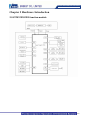
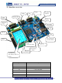
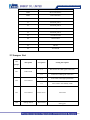
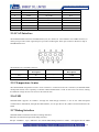
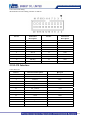
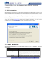
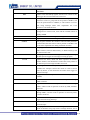
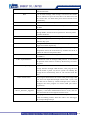
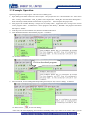
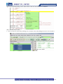
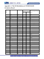
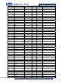
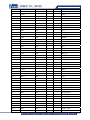
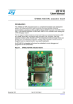
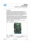
www.embedinfo.com/en
STM32F103ZE ARM-CM3 Board
User Manual
V1.0
EMBEST CO., LIMITED
Address: Room 509, Luohu Science & Technology Building,
#85 Taining Road, Shenzhen, Guangdong, China 518020
Telephone: 0086-755-25621715 or 25635626 ext. 1715
Fax: 0086-755-25616057
E-mail: [email protected] || [email protected]
Website: http://www.embedinfo.com/en
1/20
www.embedinfo.com/en
Content
CHAPTER 1 OVERVIEW .................................................................................................................. 3
CHAPTER 2 HARDWARE INTRODUCTION ...................................................................................... 4
2.0 STM32F103ZE function module.................................................................................................................4
2.1 Interface overview ........................................................................................................................................5
2.2 Jumper List ...................................................................................................................................................6
2.3 Power.............................................................................................................................................................7
2.4 Start selection................................................................................................................................................7
2.5 Clock source..................................................................................................................................................8
2.6 Reset ..............................................................................................................................................................8
2.7 Audio..............................................................................................................................................................8
2.8 Flash ..............................................................................................................................................................8
2.9 NAND Flash ..................................................................................................................................................8
2.10 NOR Flash...................................................................................................................................................8
2.11 SRAM ..........................................................................................................................................................8
2.12 Serial port....................................................................................................................................................8
2.13 SD Card Interface ......................................................................................................................................9
2.14 CAN Interface...........................................................................................................................................10
2.15 Temperature Senior..................................................................................................................................10
2.16 USB ............................................................................................................................................................10
2.17 Debug Interface ........................................................................................................................................10
2.18 LCD Interface........................................................................................................................................... 11
CHAPTER 3 SOFTWARE DEVELOPMENT AND RELEVANT PROGRAM EXAMPLES ......................... 12
3.1 MDK introduction......................................................................................................................................12
3.2 Example Introduction ................................................................................................................................12
3.3 Example Operation ....................................................................................................................................15
APPENDIX A: THE IO DISTRIBUTION OF STM32F103ZE EVALUATION BOARD ....................... 17
2/20
www.embedinfo.com/en
Chapter 1 Overview
The STM32F103ZE is an ARM embedded evaluation board produced by Embest, integrate the
STMicroelectronic ARM Cortex-M3 core-based processor STM32F103ZE, operating at a 72 MHz frequency,
with 512KB Flash memory and 64KB SRAM. The board features USB, CAN, SD Card interface, TFT-LCD,
RS232 serial interface, four 26-pin user extended interface, etc. Plenty of software examples, which can be used
in Keil MDK environment, are accompanied in CDROM.
Features:
◆ Processor:STM32F103ZE,Frequency:72MHz
◆ 2MB NOR FLASH
◆ 128KB SRAM
◆ 128MB NAND FLASH
◆ 8M byte SPI Flash
◆ RTC(Including back-up battery)
◆ Start jumper settings
◆ Optional two-way power:5VDC and USB
◆ an SD memory card interface
◆ TFT-LCD interface
◆ A temperature sensor
◆ An audio DAC output
◆ 20Pin JTAG debug interface
◆ Two RS232 serial port
◆ A USB Device interface
◆ A rocker handle with four functions to control the direction
◆ Four keys with functions: Reset, Wakeup, Temper and User button four Led lights
◆ Four LED lighter
◆ Four 8-LED output
◆ a CAN bus interface which lead by the DB9 interface
◆ a AD input
◆ Four user’s interface with 26Pin
3/20
www.embedinfo.com/en
Chapter 2 Hardware Introduction
2.0 STM32F103ZE function module
4/20
www.embedinfo.com/en
2.1 Interface overview
USB
COM1
COM2
DC power
interface
CAN
SPI FLASH
Power
choose
AD Input
knob
SPEAKER
LED
SD card
t
8LED
Five-dimension
al rocker button
JTAG
Power
instructions LED
USER key
temperature
sensor
LCD interface
NAND FLASH
RTC battery under lcd
screen
Peripherals
Description
CN1
Power JACK
P1
UART1 / Male DB9 COM2
P2
UART1 / Male DB9 COM1
P3
CAN / Male DB9
S1
RESET KEY
S2
WAKEUP KEY
S3
TAMPER KEY
S4
USER KEY
5/20
www.embedinfo.com/en
CON1
USB Device(B)Interface
CON2
SD Card Interface
CON3
JTAG Interface
CON5
FSMC LCD Interface
J1
break-out pads 1
J2
break-out pads 2
J3
break-out pads 3
J4
break-out pads 4
U3
NAND FLASH
U4
SPI FLASH
U5
NOR FLASH
U6
SRAM
U8
JOYSTICK
2.2 Jumper List
No.
jumper
description
JP1
USB related
JP2
Set options
Setting description
1-2
Disconnect the USB signal connection
2-3
connect the USB signal connection
1-2
CAN work in the high-speed mode
2-3
CAN work in the Standby mode
CAN related
JP3
CAN related
Short access
CAN load
JP4
Debug related
Short access
Connect the TRST line of the Rest and the
debug port
6/20
www.embedinfo.com/en
Cut Off
JP5
Power
supply options (Note:
only one of the group
can be short access )
JP6
DAC related
Not connect the TRST line of the Rest and
the debug port
1-2
Choose USB power supply
3-4
Choose Power Jack DC power supply
Short access
To connect the DAC output and SPEAKER
disconnection
To disconnect
SPEAKER
the
DAC
output
and
2.3 Power
STM32F103ZE Board has two power supplies; you can choose one of the following ways to supply power
through JP5:
(1) Through the motherboard power CN1 supply 5V DC.
(2) Through the motherboard USB port (CON1) supply power, the power current is less than 500mA.
The DC5V on the motherboard input (CN1) signal is negative, as follows:
The outside signal of DC5V input side (CN1) is negative, the inside is the opposite, please see the following
figure:
2.4 Start selection
STM32F103ZE Board can get started thought following three ways:
■ Start from the user's flash memory
■ Start from the system memory
■ Start from the embedded SRAM
Setting the sub-panel DIP switches (SW1 and SW2) to select the start-up mode
SW1
SW2
x
0
Start-up mode
Start from the user's flash memory
7/20
www.embedinfo.com/en
0
1
Start from the system memory
1
1
Start from the embedded SRAM
2.5 Clock source
STM32F103ZE evaluation board has two clock sources:
■ 32KHz as the RTC clock source
■ 8MHz as the MCU clock source
2.6 Reset
STM32F103ZE evaluation board has two ways to reset:
■ Use the reset button (s1) on Evaluation Board
■ If short connected JP4, then use the JTAG debug port to reset
2.7 Audio
STM32F103ZE Board can play audio files through external Speaker. The JP6 is used to control the connection
between DAC output and the Speaker.
2.8 Flash
STM32F103ZE evaluation board expanded 8MB of SPI flash. Through the SPI1 port, the chip election of this
FLASH is controlled by PB2 port.
2.9 NAND Flash
STM32F103ZE evaluation board expanded 128MB of NAND Flash(For further details, see schematic).
2.10 NOR Flash
STM32F103ZE evaluation board expanded 2MB of NOR Flash(For further details, see schematic).
2.11 SRAM
STM32F103ZE evaluation board expanded 128KB of SRAM(For further details, see schematic).
2.12 Serial port
STM32F103ZE evaluation board has two UART: UART1 (COM1) and UART2 (COM2). Two serial ports are
connected to the public DB9 connector. UART2 is support to the RTS / CTS handshake signals.
UART2 RS232 : the signal definition of Male DB9 connector:
8/20
www.embedinfo.com/en
Pin No.
Functional
Description
Pin No.
Functional
Description
1
NC
6
Connect to pin 4
2
UART2_RXD
7
UART2_RTS
3
UART2_TXD
8
UART2_CTS
4
Connect to pin 6
9
NC
5
GND
UART1 RS232 : the signal definition of public DB9 connector:
Pin No.
Functional
Description
Pin No.
Functional
Description
1
NC
6
Connect to pin 4
2
UART1_RXD
7
Connect to pin 8
3
UART1_TXD
8
Connect to pin 7
4
Connect to pin 6
9
NC
5
GND
2.13 SD Card Interface
STM32F103ZE evaluation board integrates SD card interface, supports for read/write function of SD cards.
Their connection signals are as follows.
Pin No.
SD card interface
signal
Functional Description
The counterpart of
STM32 pin
1
CD/DAT3
SD_DAT3
PC11
2
CMD
SD_CMD
PD2
3
VSS1
GND
4
VDD
+3V3
5
CLK
SD_CLK
PC12
9/20
www.embedinfo.com/en
6
VSS2
GND
7
DAT0
SD_DAT0
PC8
8
DAT1
SD_DAT1
PC9
9
DAT2
SD_DAT2
PC10
10
WP
11
NCD
12
PAD1
GND
13
PAD2
GND
NC
SD_NCD
PF11
2.14 CAN Interface
The STM32F103ZE board uses SN65HVD230 (U10) as CAN driver. CAN interface uses a DB9 connector, in
which pin 2 provides CANL signal and pin 7 provides CANH signal. These pins connect to the driver chip of
SN65HVD230 CAN.
The definition of CAN DB9 connector:
Pin No.
Functional
Description
Pin No.
Functional
Description
1,4,8,9
NC
7
CANH
2
CANL
3,5,6
GND
2.15 Temperature Senior
The STLM75M2E temperature sensors of I2C interface is connected to the I2C1 interface (at STM32F103ZE
development board). Two separately N-channel enhanced MOS-FET is used for the levels conversion, making
the different voltage devices can access to the same I2C bus.
2.16 USB
STM32F103ZE supports for USB2.0,through the USB B-type interface it can do the USB full-speed
communication. Meanwhile, through this USB interface, we can provide 5V DC (500mA current limited) for the
board.
2.17 Debug Interface
STM32F103ZE evaluation board has two debug interfaces:
■ CON3: the standard 20-pin JTAG debug interface;
■ 7 pin(SWDIO),9 pin(SWCLK)are used for SWD debug interface in CON3,and support the new ARM
10/20
www.embedinfo.com/en
Cortex-M3 serial debug.
The definition of JTAG debug interface as follows:
Pin No.
Functional
Description
Pin No.
Functional
Description
1
3.3V
2
3.3V
3
TRST
4
GND
5
TDI
6
GND
7
TMS
8
GND
9
TCK
10
GND
11
RTCK
12
GND
13
TDO
14
GND
15
RESET
16
GND
17
DBGRQ
18
GND
19
DBGACK
20
GND
2.18 LCD Interface
Color TFT LCD
Pin No.
Functional Description
I/O port
1
CS
PG12
2
RS
PF0
3
WR/SCL
PD5
4
RD
PD4
5
RESET
RESET
22
BL_GND
GND
23
BL_Control
+3V3
24
VDD
+3V3
25
VC1
+3V3
26
GND
GND
27
GND
GND
28
BL_VDD
+3V3
29
SDO
NC
30
SDI
NC
11/20
www.embedinfo.com/en
Chapter 3 Software development and relevant program
examples
3.1 MDK introduction
RealView MDK Development Suite is the latest software development tool of ARM Limited Corporation for all
kinds of Embedded Processors. It integrates the most advanced technology in this industry, including μVision3
IDE and RealView Compiler, RealView MDK supports ARM7, ARM9 and the latest Cortex-M3 Core Processor.
It has a configuration wizard for startup code and integrates flash program module, powerful device simulation,
performance analyzer and so on.
You can obtain MDK software from the CD released with STM32F103ZE Board, or you can download the latest
version from Keil website www.keil.com. Double click the installation file setup.exe, finish Keil uVision3
installation under the guidance of the installation wizard. The installation interface as follows:
3.2 Example Introduction
STM32F103ZE Evaluation Board has provided abundant examples; they can be compiled and run in Keil
uVision3 directly.
Experiment Name
Function Description
8LED
Control the 8 Nixie tubes through GPIO.
ADC
When the conversion value of ADC CHANNEL14 beyond the
simulative watchdog’s upper limit or lower limit, it will enter
into AWD interrupt and control LED1 in interrupt processing
function.
AUDIO
The program writes the audio file (wave format) into SPI
12/20
www.embedinfo.com/en
Flash, reads the audio file from SPI Flash and output it through
SPEAKER.
BKP
Read or write the backup register, check if it is correct or not,
and trigger the relevant LED at the same time.
CAN
In experiment, CAN communication works in loopback mode,
transmit or receive a group data at the speed of 100Kb/s, and
when the speed reaches to 500Kb/s, it will transmit or receive
data using interrupt mode. This implements the CAN
interface’s self-check function.
CortexM3
The program demonstrates how to use CortexM3’s bit
management to execute read, write and the variable control of
reading SRAM.
CRC
Generate CRC error-detecting code through CRC module.
DAC
Implement DA conversion through DAC module
DEBUG
The program simulates the condition when the fault parameter
is transmitted, the fault source will be printed in USART1 and
LCD, and it implements the debug simulation function.
DMA
The program demonstrates how to transmit a group data with
DMA channel (from FLASH memory to RAM memory) and
the transmission state.
EXTI
This program shows how to configure an interrupt line to get
an interrupt and trigger the interrupt processing program.
FLASH
Implement the Erase, Read and Write operation on Flash’s
definite address, and checkout the written data, lastly read it to
FLASH and print it through USART1 and LCD.
GPIO
This program has set a variety of ways to control GPIO, it also
simulates the transport control line which is used to control
JTAG by kernel, it will disconnect the JTAG when trigger an
external interrupt.
IWDG
Using SYSTICK interrupt to reload IWDG counter (every time
350MS).
LCD
Control LCD to show chars and colorful picture through
FSMC interface.
NandFlash
Implement the read and write operation to NandFlash through
FSMC, and the result of operation is shown by LED, USART1
and LCD.
NorFlash
Implement the read and write operation of external NorFlash
through FSMC, and the result of operation is shown by LED,
USART1 and LCD.
NVIC
Nested Vector Interrupt Control, it links with three clocks, and
trigger the LED using interrupt.
PWR
Control system into STOP mode, and system woke up by
EXTI interrupt.
RCC
This program demonstrates how to configure the clocks of all
kinds of interface using chip clock’s manage function, and it
13/20
www.embedinfo.com/en
implements the switch automatically between internal clock
and external clock.
RTC
Use for clock manage, when startup, if it has not set clock’s
time, it will have a tip to set time, then it can show time, and
the clock’s time can hold when power down because of on
board battery.
SDIO
Implement read and write operation of SD card through SDIO.
SPI
SPI mode can control the read and write operation on M25P64
FLASH.
SRAM
Implement the read and write operation of external SRAM
through FSMC, and the result of operation is shown by LED、
USART1 and LCD.
SYSTICK
It shows how to configure SYSTICK to get 1ms output.
TIM1
Through configuration, it can output clock waveform with
different duty cycle.
TIM
Configure the clock function, output different frequency value,
trigger four LEDs respectively.
Tsensor
Get temperature data through hyper sensitivity digital
temperature sensor, the result shows by USART1 and LCD, it
gathers the real-time temperature data.
USART
Communicate with PC through crossover serial port line
(115200b/s).
USB(JoyStickMouse)
Communicate with PC through USB protocol; it can control
the position of the mouse in screen by direction keys in rocker
key-press.
USB(Mass_Storage)
Implement the conversion between USB data and SD card
storage interface through USB interface, after plug SD card
and the board is power on, the PC system can identify the
storage device automatically, then we can read and write the
files.
USB(Virtual Com)
This program demonstrates the virtual COM port through USB
port, users can output data through normal COM 1 (or 0), and
this data can be shown by virtual COM port (but it need to
configure the drive program of virtual COM port before
experiment).
USB
(Device_Firmware_Upgrade)
Download this program to FLASH (after update the drive
program), it will add a USB hardware device in PC, then we
can control this device through the software in PC.
WWDG
This program demonstrates how to set and update the count
value of watchdog counter, when this value is 0 it will trigger
the corresponding interrupt.
14/20
www.embedinfo.com/en
3.3 Example Operation
Operating sequence of one program(take the case of EXTI_Test)
1. Open EXTI_Test folder(There are 6 files:Project - store project files,Inc- store head files,Src- store source
files,Listing- store link files,Run_In_Flash- store compile files,Read_Me- store document description)
,
Enter into Project folder, double-click EXTI.Uv2 project file, then will open this project file。
2. This project file includes StartUp(storage area of startup codes),Application File(storage area of main
source program codes),Common File(source program’s files library),ReadMe(the program’s document
description)folders。
3. Link the power line and emulator line (between ULINK2 and JTAG)
4. Click Flash/Download to download the program:as follows:
Or click this shortcut icon:
Click to download program
5. After download, execute Debug/Start/Stop Debug Session(Ctrl+F5) to have a debug,as follows:
Or shortcut icon:
to enter into debug。
After click, the main displaying area will show assembly code, if you want to see source codes, you can
15/20
www.embedinfo.com/en
right click mouse before Step, choose “Show Source Code for current Address”. As follows:
There will show source codes。
6. We can make use of the shortcut debug icon in window execute the Debug process, the icon as follows:
16/20
www.embedinfo.com/en
Appendix A: The IO Distribution of STM32F103ZE
Evaluation Board
TQFP100
Pins
Type
Level
Input
Output
The
IO
assign
of
STM32F103ZE Evaluation
Board
1
PE2
I/O
A23
2
PE3
I/O
A19
3
PE4
I/O
A20
4
PE5
I/O
A21
5
PE6
I/O
A22
6
VBAT
Input
VBAT
7
PC13
I/O
Tamper Button
8
PC14
I/O
X1(OSC32_IN)
9
PC15
I/O
X1(OSC32_OUT)
10
PF0
I/O
A0
11
PF1
I/O
A1
12
PF2
I/O
A2
13
PF3
I/O
A3
14
PF4
I/O
A4
15
PF5
I/O
A5
16
VSS5
GND
17
VDD5
+3V3
18
PF6
I/O
LED1
19
PF7
I/O
LED2
20
PF8
I/O
LED3
21
PF9
I/O
LED4
22
PF10
I/O
PF10
23
OSC_IN
OSC_IN
24
OSC_OUT
OSC_OUT
25
NRST
Input
RESET Button
26
PC0
I/O
PC0
27
PC1
I/O
PC1
28
PC2
I/O
PC2
29
PC3
I/O
PC3
30
VSSA
GND
31
VREF-
GND
32
VREF+
+3V3
33
VDDA
+3V3
34
PA0/WKUP
I/O
WAKEUP
35
PA1
I/O
PA1
17/20
www.embedinfo.com/en
36
PA2
I/O
TXD2
37
PA3
I/O
RXD2
38
VSS4
GND
39
VDD4
+3V3
40
PA4
I/O
DAC_OUT1
41
PA5
I/O
SPI1_CLK
42
PA6
I/O
SPI1_MISO
43
PA7
I/O
SPI1_MOSI
44
PC4
I/O
PC4
45
PC5
I/O
PC5
46
PB0
I/O
PB0
47
PB1
I/O
PB1
48
PB2
I/O
SPI1_CS
49
PF11
I/O
SD_NCD
50
PF12
I/O
A6
51
VSS6
GND
52
VDD6
+3V3
53
PF13
I/O
A7
54
PF14
I/O
A8
55
PF15
I/O
A9
56
PG0
I/O
A10
57
PG1
I/O
A11
58
PE7
I/O
D4
59
PE8
I/O
D5
60
PE9
I/O
D6
61
VSS7
GND
62
VDD7
+3V3
63
PE10
I/O
D7
64
PE11
I/O
D8
65
PE12
I/O
D9
66
PE13
I/O
D10
67
PE14
I/O
D11
68
PE15
I/O
D12
69
PB10
I/O
PB10
70
PB11
I/O
PB11
71
VSS1
GND
72
VDD1
+3V3
73
PB12
I/O
PB12
74
PB13
I/O
PB13
75
PB14
I/O
USB_DIS
76
PB15
I/O
PB15
77
PD8
I/O
D13
78
PD9
I/O
D14
79
PD10
I/O
D15
80
PD11
I/O
A16
18/20
www.embedinfo.com/en
81
PD12
I/O
A17
82
PD13
I/O
A18
83
VSS8
GND
84
VDD8
+3V3
85
PD14
I/O
D0
86
PD15
I/O
D1
87
PG2
I/O
A12
88
PG3
I/O
A13
89
PG4
I/O
A14
90
PG5
I/O
A15
91
PG6
I/O
FSMC_INT2
92
PG7
I/O
JOY_SEL
93
PG8
I/O
USER
94
VSS9
GND
95
VDD9
+3V3
96
PC6
I/O
PC6
97
PC7
I/O
PC7
98
PC8
I/O
SD_DATA0
99
PC9
I/O
SD_DATA1
100
PA8
I/O
BL_CN
101
PA9
I/O
TXD1
102
PA10
I/O
RXD1
103
PA11
I/O
USB_DM
104
PA12
I/O
USB_DP
105
PA13
I/O
TMS
106
NC
107
VSS2
GND
108
VDD2
+3V3
109
PA14
I/O
TCK
110
PA15
I/O
TDI
111
PC10
I/O
SD_DATA2
112
PC11
I/O
SD_DATA3
113
PC12
I/O
SD_CLK
114
PD0
I/O
D2
115
PD1
I/O
D3
116
PD2
I/O
SD_CMD
117
PD3
I/O
JOY_DOWN
118
PD4
I/O
FSMC_NOE
119
PD5
I/O
FSMC_NWE
120
VSS10
GND
121
VDD10
+3V3
122
PD6
I/O
FSMC_NWAIT
123
PD7
I/O
FSMC_NCE2
124
PG9
I/O
FSMC_NE2
125
PG10
I/O
FSMC_NE3
19/20
www.embedinfo.com/en
126
PG11
I/O
PG11
127
PG12
I/O
FSMC_NE4
128
PG13
I/O
JOY_RIGHT
129
PG14
I/O
JOY_LEFT
130
VSS11
GND
131
VDD11
+3V3
132
PG15
I/O
JOY_UP
133
PB3
I/O
TDO
134
PB4
I/O
TRST
135
PB5
I/O
TEMP_INT
136
PB6
I/O
TEMP_SCL
137
PB7
I/O
TEMP_SDA
138
BOOT0
139
PB8
I/O
CAN_RX
140
PB9
I/O
CAN_TX
141
PE0
I/O
FSMC_NBL0
142
PE1
I/O
FSMC_NBL1
143
VSS3
GND
144
VDD3
+3V3
SW1
20/20